KR101891458B1 - Semiconductor device having iii-v semiconductor material layer - Google Patents
Semiconductor device having iii-v semiconductor material layerDownload PDFInfo
- Publication number
- KR101891458B1 KR101891458B1KR1020177030300AKR20177030300AKR101891458B1KR 101891458 B1KR101891458 B1KR 101891458B1KR 1020177030300 AKR1020177030300 AKR 1020177030300AKR 20177030300 AKR20177030300 AKR 20177030300AKR 101891458 B1KR101891458 B1KR 101891458B1
- Authority
- KR
- South Korea
- Prior art keywords
- source
- drain regions
- layer
- iii
- type
- Prior art date
- Legal status (The legal status is an assumption and is not a legal conclusion. Google has not performed a legal analysis and makes no representation as to the accuracy of the status listed.)
- Active
Links
- 239000000463materialSubstances0.000titleclaimsabstractdescription130
- 239000004065semiconductorSubstances0.000titleclaimsabstractdescription66
- 238000000034methodMethods0.000claimsabstractdescription92
- 229910052751metalInorganic materials0.000claimsabstractdescription34
- 239000002184metalSubstances0.000claimsabstractdescription34
- 239000002070nanowireSubstances0.000claimsabstractdescription32
- 239000000758substrateSubstances0.000claimsdescription48
- 229910052710siliconInorganic materials0.000claimsdescription34
- 239000010703siliconSubstances0.000claimsdescription32
- 229910052732germaniumInorganic materials0.000claimsdescription28
- GNPVGFCGXDBREM-UHFFFAOYSA-Ngermanium atomChemical compound[Ge]GNPVGFCGXDBREM-UHFFFAOYSA-N0.000claimsdescription26
- 239000012212insulatorSubstances0.000claimsdescription25
- XUIMIQQOPSSXEZ-UHFFFAOYSA-NSiliconChemical compound[Si]XUIMIQQOPSSXEZ-UHFFFAOYSA-N0.000claimsdescription24
- 239000002019doping agentSubstances0.000claimsdescription21
- 229910000577Silicon-germaniumInorganic materials0.000claimsdescription19
- 229910052782aluminiumInorganic materials0.000claimsdescription10
- 229910052785arsenicInorganic materials0.000claimsdescription10
- XAGFODPZIPBFFR-UHFFFAOYSA-NaluminiumChemical compound[Al]XAGFODPZIPBFFR-UHFFFAOYSA-N0.000claimsdescription8
- RQNWIZPPADIBDY-UHFFFAOYSA-Narsenic atomChemical compound[As]RQNWIZPPADIBDY-UHFFFAOYSA-N0.000claimsdescription8
- 229910052738indiumInorganic materials0.000claimsdescription7
- 229910052733galliumInorganic materials0.000claimsdescription6
- 229910052787antimonyInorganic materials0.000claimsdescription5
- APFVFJFRJDLVQX-UHFFFAOYSA-Nindium atomChemical compound[In]APFVFJFRJDLVQX-UHFFFAOYSA-N0.000claimsdescription5
- GYHNNYVSQQEPJS-UHFFFAOYSA-NGalliumChemical compound[Ga]GYHNNYVSQQEPJS-UHFFFAOYSA-N0.000claimsdescription4
- LEVVHYCKPQWKOP-UHFFFAOYSA-N[Si].[Ge]Chemical compound[Si].[Ge]LEVVHYCKPQWKOP-UHFFFAOYSA-N0.000claimsdescription4
- WATWJIUSRGPENY-UHFFFAOYSA-Nantimony atomChemical compound[Sb]WATWJIUSRGPENY-UHFFFAOYSA-N0.000claimsdescription4
- BHEPBYXIRTUNPN-UHFFFAOYSA-Nhydridophosphorus(.) (triplet)Chemical compound[PH]BHEPBYXIRTUNPN-UHFFFAOYSA-N0.000claims2
- 239000011229interlayerSubstances0.000abstractdescription4
- 230000003071parasitic effectEffects0.000abstractdescription3
- 150000002739metalsChemical class0.000abstractdescription2
- 239000010410layerSubstances0.000description104
- 230000008569processEffects0.000description32
- 238000000151depositionMethods0.000description29
- 230000008021depositionEffects0.000description19
- 238000004891communicationMethods0.000description17
- 229910045601alloyInorganic materials0.000description8
- 239000000956alloySubstances0.000description8
- 238000013461designMethods0.000description7
- 238000011065in-situ storageMethods0.000description7
- PXHVJJICTQNCMI-UHFFFAOYSA-NNickelChemical compound[Ni]PXHVJJICTQNCMI-UHFFFAOYSA-N0.000description6
- 238000005229chemical vapour depositionMethods0.000description6
- 239000003989dielectric materialSubstances0.000description6
- 229910052698phosphorusInorganic materials0.000description6
- 125000006850spacer groupChemical group0.000description6
- VYPSYNLAJGMNEJ-UHFFFAOYSA-NSilicium dioxideChemical compoundO=[Si]=OVYPSYNLAJGMNEJ-UHFFFAOYSA-N0.000description5
- 230000015572biosynthetic processEffects0.000description5
- 238000005137deposition processMethods0.000description5
- 238000005530etchingMethods0.000description5
- WPYVAWXEWQSOGY-UHFFFAOYSA-Nindium antimonideChemical compound[Sb]#[In]WPYVAWXEWQSOGY-UHFFFAOYSA-N0.000description5
- 238000005468ion implantationMethods0.000description5
- 238000002955isolationMethods0.000description5
- 229910021332silicideInorganic materials0.000description5
- FVBUAEGBCNSCDD-UHFFFAOYSA-Nsilicide(4-)Chemical compound[Si-4]FVBUAEGBCNSCDD-UHFFFAOYSA-N0.000description5
- ZOXJGFHDIHLPTG-UHFFFAOYSA-NBoronChemical compound[B]ZOXJGFHDIHLPTG-UHFFFAOYSA-N0.000description4
- OAICVXFJPJFONN-UHFFFAOYSA-NPhosphorusChemical compound[P]OAICVXFJPJFONN-UHFFFAOYSA-N0.000description4
- 229910052581Si3N4Inorganic materials0.000description4
- 229910004298SiO 2Inorganic materials0.000description4
- 238000000137annealingMethods0.000description4
- 125000004429atomChemical group0.000description4
- 230000008901benefitEffects0.000description4
- 229910052796boronInorganic materials0.000description4
- 150000001875compoundsChemical class0.000description4
- 238000007796conventional methodMethods0.000description4
- 230000006870functionEffects0.000description4
- 239000000203mixtureSubstances0.000description4
- 238000000059patterningMethods0.000description4
- 239000011574phosphorusSubstances0.000description4
- BASFCYQUMIYNBI-UHFFFAOYSA-NplatinumChemical compound[Pt]BASFCYQUMIYNBI-UHFFFAOYSA-N0.000description4
- 239000002243precursorSubstances0.000description4
- 238000012545processingMethods0.000description4
- HQVNEWCFYHHQES-UHFFFAOYSA-Nsilicon nitrideChemical compoundN12[Si]34N5[Si]62N3[Si]51N64HQVNEWCFYHHQES-UHFFFAOYSA-N0.000description4
- WFKWXMTUELFFGS-UHFFFAOYSA-NtungstenChemical compound[W]WFKWXMTUELFFGS-UHFFFAOYSA-N0.000description4
- 229910052721tungstenInorganic materials0.000description4
- 239000010937tungstenSubstances0.000description4
- 238000000231atomic layer depositionMethods0.000description3
- 229910052799carbonInorganic materials0.000description3
- 238000009792diffusion processMethods0.000description3
- 230000000873masking effectEffects0.000description3
- 229910044991metal oxideInorganic materials0.000description3
- 150000004706metal oxidesChemical class0.000description3
- 229910052759nickelInorganic materials0.000description3
- HBMJWWWQQXIZIP-UHFFFAOYSA-Nsilicon carbideChemical compound[Si+]#[C-]HBMJWWWQQXIZIP-UHFFFAOYSA-N0.000description3
- 229910010271silicon carbideInorganic materials0.000description3
- IJGRMHOSHXDMSA-UHFFFAOYSA-NAtomic nitrogenChemical compoundN#NIJGRMHOSHXDMSA-UHFFFAOYSA-N0.000description2
- OKTJSMMVPCPJKN-UHFFFAOYSA-NCarbonChemical compound[C]OKTJSMMVPCPJKN-UHFFFAOYSA-N0.000description2
- KDLHZDBZIXYQEI-UHFFFAOYSA-NPalladiumChemical compound[Pd]KDLHZDBZIXYQEI-UHFFFAOYSA-N0.000description2
- NPXOKRUENSOPAO-UHFFFAOYSA-NRaney nickelChemical compound[Al].[Ni]NPXOKRUENSOPAO-UHFFFAOYSA-N0.000description2
- 229910000676Si alloyInorganic materials0.000description2
- RTAQQCXQSZGOHL-UHFFFAOYSA-NTitaniumChemical compound[Ti]RTAQQCXQSZGOHL-UHFFFAOYSA-N0.000description2
- 238000013459approachMethods0.000description2
- 239000012159carrier gasSubstances0.000description2
- 239000000460chlorineSubstances0.000description2
- 229910017052cobaltInorganic materials0.000description2
- 239000010941cobaltSubstances0.000description2
- GUTLYIVDDKVIGB-UHFFFAOYSA-Ncobalt atomChemical compound[Co]GUTLYIVDDKVIGB-UHFFFAOYSA-N0.000description2
- 239000007789gasSubstances0.000description2
- 238000000171gas-source molecular beam epitaxyMethods0.000description2
- 229910000078germaneInorganic materials0.000description2
- SCCCLDWUZODEKG-UHFFFAOYSA-NgermanideChemical compound[GeH3-]SCCCLDWUZODEKG-UHFFFAOYSA-N0.000description2
- 239000011521glassSubstances0.000description2
- 229910000449hafnium oxideInorganic materials0.000description2
- WIHZLLGSGQNAGK-UHFFFAOYSA-Nhafnium(4+);oxygen(2-)Chemical compound[O-2].[O-2].[Hf+4]WIHZLLGSGQNAGK-UHFFFAOYSA-N0.000description2
- MRELNEQAGSRDBK-UHFFFAOYSA-Nlanthanum(3+);oxygen(2-)Chemical compound[O-2].[O-2].[O-2].[La+3].[La+3]MRELNEQAGSRDBK-UHFFFAOYSA-N0.000description2
- 238000004519manufacturing processMethods0.000description2
- PCLURTMBFDTLSK-UHFFFAOYSA-Nnickel platinumChemical compound[Ni].[Pt]PCLURTMBFDTLSK-UHFFFAOYSA-N0.000description2
- 229910052697platinumInorganic materials0.000description2
- -1polytetrafluoroethylenePolymers0.000description2
- 238000001289rapid thermal chemical vapour depositionMethods0.000description2
- 235000012239silicon dioxideNutrition0.000description2
- 239000000377silicon dioxideSubstances0.000description2
- 229910052709silverInorganic materials0.000description2
- 239000004332silverSubstances0.000description2
- 229910052719titaniumInorganic materials0.000description2
- 239000010936titaniumSubstances0.000description2
- 238000000038ultrahigh vacuum chemical vapour depositionMethods0.000description2
- ZAMOUSCENKQFHK-UHFFFAOYSA-NChlorine atomChemical compound[Cl]ZAMOUSCENKQFHK-UHFFFAOYSA-N0.000description1
- 229910001218Gallium arsenideInorganic materials0.000description1
- VEXZGXHMUGYJMC-UHFFFAOYSA-NHydrochloric acidChemical compoundClVEXZGXHMUGYJMC-UHFFFAOYSA-N0.000description1
- CPELXLSAUQHCOX-UHFFFAOYSA-NHydrogen bromideChemical compoundBrCPELXLSAUQHCOX-UHFFFAOYSA-N0.000description1
- 229910000673Indium arsenideInorganic materials0.000description1
- 229910000990Ni alloyInorganic materials0.000description1
- KJTLSVCANCCWHF-UHFFFAOYSA-NRutheniumChemical compound[Ru]KJTLSVCANCCWHF-UHFFFAOYSA-N0.000description1
- BQCADISMDOOEFD-UHFFFAOYSA-NSilverChemical compound[Ag]BQCADISMDOOEFD-UHFFFAOYSA-N0.000description1
- ATJFFYVFTNAWJD-UHFFFAOYSA-NTinChemical compound[Sn]ATJFFYVFTNAWJD-UHFFFAOYSA-N0.000description1
- GWEVSGVZZGPLCZ-UHFFFAOYSA-NTitan oxideChemical compoundO=[Ti]=OGWEVSGVZZGPLCZ-UHFFFAOYSA-N0.000description1
- NRTOMJZYCJJWKI-UHFFFAOYSA-NTitanium nitrideChemical compound[Ti]#NNRTOMJZYCJJWKI-UHFFFAOYSA-N0.000description1
- HCHKCACWOHOZIP-UHFFFAOYSA-NZincChemical compound[Zn]HCHKCACWOHOZIP-UHFFFAOYSA-N0.000description1
- BYDQGSVXQDOSJJ-UHFFFAOYSA-N[Ge].[Au]Chemical compound[Ge].[Au]BYDQGSVXQDOSJJ-UHFFFAOYSA-N0.000description1
- XWCMFHPRATWWFO-UHFFFAOYSA-N[O-2].[Ta+5].[Sc+3].[O-2].[O-2].[O-2]Chemical compound[O-2].[Ta+5].[Sc+3].[O-2].[O-2].[O-2]XWCMFHPRATWWFO-UHFFFAOYSA-N0.000description1
- ILCYGSITMBHYNK-UHFFFAOYSA-N[Si]=O.[Hf]Chemical compound[Si]=O.[Hf]ILCYGSITMBHYNK-UHFFFAOYSA-N0.000description1
- 239000011149active materialSubstances0.000description1
- 239000012790adhesive layerSubstances0.000description1
- 238000004458analytical methodMethods0.000description1
- 238000003491arrayMethods0.000description1
- RBFQJDQYXXHULB-UHFFFAOYSA-NarsaneChemical compound[AsH3]RBFQJDQYXXHULB-UHFFFAOYSA-N0.000description1
- VKJLWXGJGDEGSO-UHFFFAOYSA-Nbarium(2+);oxygen(2-);titanium(4+)Chemical compound[O-2].[O-2].[O-2].[Ti+4].[Ba+2]VKJLWXGJGDEGSO-UHFFFAOYSA-N0.000description1
- 230000004888barrier functionEffects0.000description1
- 229910001423beryllium ionInorganic materials0.000description1
- 229910052793cadmiumInorganic materials0.000description1
- BDOSMKKIYDKNTQ-UHFFFAOYSA-Ncadmium atomChemical compound[Cd]BDOSMKKIYDKNTQ-UHFFFAOYSA-N0.000description1
- 239000003990capacitorSubstances0.000description1
- 239000000969carrierSubstances0.000description1
- 229910052801chlorineInorganic materials0.000description1
- 230000000295complement effectEffects0.000description1
- 238000010276constructionMethods0.000description1
- 230000003247decreasing effectEffects0.000description1
- VXGHASBVNMHGDI-UHFFFAOYSA-NdigermaneChemical compound[Ge][Ge]VXGHASBVNMHGDI-UHFFFAOYSA-N0.000description1
- 229910001873dinitrogenInorganic materials0.000description1
- KPUWHANPEXNPJT-UHFFFAOYSA-NdisiloxaneChemical class[SiH3]O[SiH3]KPUWHANPEXNPJT-UHFFFAOYSA-N0.000description1
- 230000000694effectsEffects0.000description1
- 239000007772electrode materialSubstances0.000description1
- 230000005670electromagnetic radiationEffects0.000description1
- 238000005516engineering processMethods0.000description1
- 238000011066ex-situ storageMethods0.000description1
- 230000005669field effectEffects0.000description1
- 229940104869fluorosilicateDrugs0.000description1
- 238000005755formation reactionMethods0.000description1
- PCHJSUWPFVWCPO-UHFFFAOYSA-NgoldChemical compound[Au]PCHJSUWPFVWCPO-UHFFFAOYSA-N0.000description1
- 229910052737goldInorganic materials0.000description1
- 239000010931goldSubstances0.000description1
- 229910052736halogenInorganic materials0.000description1
- 150000002367halogensChemical class0.000description1
- 230000020169heat generationEffects0.000description1
- 229910052739hydrogenInorganic materials0.000description1
- 239000001257hydrogenSubstances0.000description1
- 125000004435hydrogen atomChemical class[H]*0.000description1
- 230000006872improvementEffects0.000description1
- RPQDHPTXJYYUPQ-UHFFFAOYSA-Nindium arsenideChemical compound[In]#[As]RPQDHPTXJYYUPQ-UHFFFAOYSA-N0.000description1
- 239000011810insulating materialSubstances0.000description1
- JQJCSZOEVBFDKO-UHFFFAOYSA-Nlead zincChemical compound[Zn].[Pb]JQJCSZOEVBFDKO-UHFFFAOYSA-N0.000description1
- 230000007774longtermEffects0.000description1
- 238000004518low pressure chemical vapour depositionMethods0.000description1
- 238000013507mappingMethods0.000description1
- 238000012986modificationMethods0.000description1
- 230000004048modificationEffects0.000description1
- 150000004767nitridesChemical class0.000description1
- 229910052756noble gasInorganic materials0.000description1
- NJPPVKZQTLUDBO-UHFFFAOYSA-NnovaluronChemical compoundC1=C(Cl)C(OC(F)(F)C(OC(F)(F)F)F)=CC=C1NC(=O)NC(=O)C1=C(F)C=CC=C1FNJPPVKZQTLUDBO-UHFFFAOYSA-N0.000description1
- BCCOBQSFUDVTJQ-UHFFFAOYSA-NoctafluorocyclobutaneChemical compoundFC1(F)C(F)(F)C(F)(F)C1(F)FBCCOBQSFUDVTJQ-UHFFFAOYSA-N0.000description1
- 235000019407octafluorocyclobutaneNutrition0.000description1
- 229920000620organic polymerPolymers0.000description1
- TWNQGVIAIRXVLR-UHFFFAOYSA-Noxo(oxoalumanyloxy)alumaneChemical compoundO=[Al]O[Al]=OTWNQGVIAIRXVLR-UHFFFAOYSA-N0.000description1
- KJXBRHIPHIVJCS-UHFFFAOYSA-Noxo(oxoalumanyloxy)lanthanumChemical compoundO=[Al]O[La]=OKJXBRHIPHIVJCS-UHFFFAOYSA-N0.000description1
- SIWVEOZUMHYXCS-UHFFFAOYSA-Noxo(oxoyttriooxy)yttriumChemical compoundO=[Y]O[Y]=OSIWVEOZUMHYXCS-UHFFFAOYSA-N0.000description1
- BPUBBGLMJRNUCC-UHFFFAOYSA-Noxygen(2-);tantalum(5+)Chemical compound[O-2].[O-2].[O-2].[O-2].[O-2].[Ta+5].[Ta+5]BPUBBGLMJRNUCC-UHFFFAOYSA-N0.000description1
- RVTZCBVAJQQJTK-UHFFFAOYSA-Noxygen(2-);zirconium(4+)Chemical compound[O-2].[O-2].[Zr+4]RVTZCBVAJQQJTK-UHFFFAOYSA-N0.000description1
- 229910052763palladiumInorganic materials0.000description1
- 238000005240physical vapour depositionMethods0.000description1
- 229910021420polycrystalline siliconInorganic materials0.000description1
- 229920005591polysiliconPolymers0.000description1
- 229920001343polytetrafluoroethylenePolymers0.000description1
- 239000004810polytetrafluoroethyleneSubstances0.000description1
- 239000011148porous materialSubstances0.000description1
- 229910052707rutheniumInorganic materials0.000description1
- 229910001925ruthenium oxideInorganic materials0.000description1
- WOCIAKWEIIZHES-UHFFFAOYSA-Nruthenium(iv) oxideChemical compoundO=[Ru]=OWOCIAKWEIIZHES-UHFFFAOYSA-N0.000description1
- 238000004626scanning electron microscopyMethods0.000description1
- 238000000926separation methodMethods0.000description1
- 229910052814silicon oxideInorganic materials0.000description1
- 238000004088simulationMethods0.000description1
- 239000002356single layerSubstances0.000description1
- 239000007787solidSubstances0.000description1
- VEALVRVVWBQVSL-UHFFFAOYSA-Nstrontium titanateChemical compound[Sr+2].[O-][Ti]([O-])=OVEALVRVVWBQVSL-UHFFFAOYSA-N0.000description1
- CZXRMHUWVGPWRM-UHFFFAOYSA-Nstrontium;barium(2+);oxygen(2-);titanium(4+)Chemical compound[O-2].[O-2].[O-2].[O-2].[Ti+4].[Sr+2].[Ba+2]CZXRMHUWVGPWRM-UHFFFAOYSA-N0.000description1
- 239000000126substanceSubstances0.000description1
- 229910052715tantalumInorganic materials0.000description1
- GUVRBAGPIYLISA-UHFFFAOYSA-Ntantalum atomChemical compound[Ta]GUVRBAGPIYLISA-UHFFFAOYSA-N0.000description1
- MZLGASXMSKOWSE-UHFFFAOYSA-Ntantalum nitrideChemical compound[Ta]#NMZLGASXMSKOWSE-UHFFFAOYSA-N0.000description1
- 229910001936tantalum oxideInorganic materials0.000description1
- 229910052714telluriumInorganic materials0.000description1
- PORWMNRCUJJQNO-UHFFFAOYSA-Ntellurium atomChemical compound[Te]PORWMNRCUJJQNO-UHFFFAOYSA-N0.000description1
- 238000002230thermal chemical vapour depositionMethods0.000description1
- 229910052718tinInorganic materials0.000description1
- OGIDPMRJRNCKJF-UHFFFAOYSA-Ntitanium oxideInorganic materials[Ti]=OOGIDPMRJRNCKJF-UHFFFAOYSA-N0.000description1
- 229910052725zincInorganic materials0.000description1
- 239000011701zincSubstances0.000description1
- 229910001928zirconium oxideInorganic materials0.000description1
- GFQYVLUOOAAOGM-UHFFFAOYSA-Nzirconium(iv) silicateChemical compound[Zr+4].[O-][Si]([O-])([O-])[O-]GFQYVLUOOAAOGM-UHFFFAOYSA-N0.000description1
Images


Classifications
- H—ELECTRICITY
- H10—SEMICONDUCTOR DEVICES; ELECTRIC SOLID-STATE DEVICES NOT OTHERWISE PROVIDED FOR
- H10D—INORGANIC ELECTRIC SEMICONDUCTOR DEVICES
- H10D30/00—Field-effect transistors [FET]
- H10D30/60—Insulated-gate field-effect transistors [IGFET]
- H10D30/64—Double-diffused metal-oxide semiconductor [DMOS] FETs
- H10D30/66—Vertical DMOS [VDMOS] FETs
- H10D30/663—Vertical DMOS [VDMOS] FETs having both source contacts and drain contacts on the same surface, i.e. up-drain VDMOS
- H—ELECTRICITY
- H10—SEMICONDUCTOR DEVICES; ELECTRIC SOLID-STATE DEVICES NOT OTHERWISE PROVIDED FOR
- H10D—INORGANIC ELECTRIC SEMICONDUCTOR DEVICES
- H10D30/00—Field-effect transistors [FET]
- H10D30/60—Insulated-gate field-effect transistors [IGFET]
- H10D30/67—Thin-film transistors [TFT]
- H10D30/6704—Thin-film transistors [TFT] having supplementary regions or layers in the thin films or in the insulated bulk substrates for controlling properties of the device
- H10D30/6713—Thin-film transistors [TFT] having supplementary regions or layers in the thin films or in the insulated bulk substrates for controlling properties of the device characterised by the properties of the source or drain regions, e.g. compositions or sectional shapes
- H01L27/092—
- H—ELECTRICITY
- H01—ELECTRIC ELEMENTS
- H01L—SEMICONDUCTOR DEVICES NOT COVERED BY CLASS H10
- H01L21/00—Processes or apparatus adapted for the manufacture or treatment of semiconductor or solid state devices or of parts thereof
- H01L21/70—Manufacture or treatment of devices consisting of a plurality of solid state components formed in or on a common substrate or of parts thereof; Manufacture of integrated circuit devices or of parts thereof
- H01L21/71—Manufacture of specific parts of devices defined in group H01L21/70
- H01L21/768—Applying interconnections to be used for carrying current between separate components within a device comprising conductors and dielectrics
- H01L21/76801—Applying interconnections to be used for carrying current between separate components within a device comprising conductors and dielectrics characterised by the formation and the after-treatment of the dielectrics, e.g. smoothing
- H01L21/76802—Applying interconnections to be used for carrying current between separate components within a device comprising conductors and dielectrics characterised by the formation and the after-treatment of the dielectrics, e.g. smoothing by forming openings in dielectrics
- H01L21/76805—Applying interconnections to be used for carrying current between separate components within a device comprising conductors and dielectrics characterised by the formation and the after-treatment of the dielectrics, e.g. smoothing by forming openings in dielectrics the opening being a via or contact hole penetrating the underlying conductor
- H—ELECTRICITY
- H01—ELECTRIC ELEMENTS
- H01L—SEMICONDUCTOR DEVICES NOT COVERED BY CLASS H10
- H01L21/00—Processes or apparatus adapted for the manufacture or treatment of semiconductor or solid state devices or of parts thereof
- H01L21/70—Manufacture or treatment of devices consisting of a plurality of solid state components formed in or on a common substrate or of parts thereof; Manufacture of integrated circuit devices or of parts thereof
- H01L21/71—Manufacture of specific parts of devices defined in group H01L21/70
- H01L21/768—Applying interconnections to be used for carrying current between separate components within a device comprising conductors and dielectrics
- H01L21/76838—Applying interconnections to be used for carrying current between separate components within a device comprising conductors and dielectrics characterised by the formation and the after-treatment of the conductors
- H01L21/76886—Modifying permanently or temporarily the pattern or the conductivity of conductive members, e.g. formation of alloys, reduction of contact resistances
- H—ELECTRICITY
- H01—ELECTRIC ELEMENTS
- H01L—SEMICONDUCTOR DEVICES NOT COVERED BY CLASS H10
- H01L21/00—Processes or apparatus adapted for the manufacture or treatment of semiconductor or solid state devices or of parts thereof
- H01L21/70—Manufacture or treatment of devices consisting of a plurality of solid state components formed in or on a common substrate or of parts thereof; Manufacture of integrated circuit devices or of parts thereof
- H01L21/71—Manufacture of specific parts of devices defined in group H01L21/70
- H01L21/768—Applying interconnections to be used for carrying current between separate components within a device comprising conductors and dielectrics
- H01L21/76838—Applying interconnections to be used for carrying current between separate components within a device comprising conductors and dielectrics characterised by the formation and the after-treatment of the conductors
- H01L21/76895—Local interconnects; Local pads, as exemplified by patent document EP0896365
- H01L21/823821—
- H01L27/0924—
- H01L29/0847—
- H01L29/41791—
- H01L29/66545—
- H01L29/78—
- H01L29/7809—
- H—ELECTRICITY
- H10—SEMICONDUCTOR DEVICES; ELECTRIC SOLID-STATE DEVICES NOT OTHERWISE PROVIDED FOR
- H10D—INORGANIC ELECTRIC SEMICONDUCTOR DEVICES
- H10D30/00—Field-effect transistors [FET]
- H10D30/60—Insulated-gate field-effect transistors [IGFET]
- H—ELECTRICITY
- H10—SEMICONDUCTOR DEVICES; ELECTRIC SOLID-STATE DEVICES NOT OTHERWISE PROVIDED FOR
- H10D—INORGANIC ELECTRIC SEMICONDUCTOR DEVICES
- H10D30/00—Field-effect transistors [FET]
- H10D30/60—Insulated-gate field-effect transistors [IGFET]
- H10D30/62—Fin field-effect transistors [FinFET]
- H10D30/6219—Fin field-effect transistors [FinFET] characterised by the source or drain electrodes
- H—ELECTRICITY
- H10—SEMICONDUCTOR DEVICES; ELECTRIC SOLID-STATE DEVICES NOT OTHERWISE PROVIDED FOR
- H10D—INORGANIC ELECTRIC SEMICONDUCTOR DEVICES
- H10D30/00—Field-effect transistors [FET]
- H10D30/60—Insulated-gate field-effect transistors [IGFET]
- H10D30/67—Thin-film transistors [TFT]
- H10D30/6729—Thin-film transistors [TFT] characterised by the electrodes
- H10D30/673—Thin-film transistors [TFT] characterised by the electrodes characterised by the shapes, relative sizes or dispositions of the gate electrodes
- H10D30/6735—Thin-film transistors [TFT] characterised by the electrodes characterised by the shapes, relative sizes or dispositions of the gate electrodes having gates fully surrounding the channels, e.g. gate-all-around
- H—ELECTRICITY
- H10—SEMICONDUCTOR DEVICES; ELECTRIC SOLID-STATE DEVICES NOT OTHERWISE PROVIDED FOR
- H10D—INORGANIC ELECTRIC SEMICONDUCTOR DEVICES
- H10D30/00—Field-effect transistors [FET]
- H10D30/60—Insulated-gate field-effect transistors [IGFET]
- H10D30/67—Thin-film transistors [TFT]
- H10D30/674—Thin-film transistors [TFT] characterised by the active materials
- H10D30/6741—Group IV materials, e.g. germanium or silicon carbide
- H10D30/6743—Silicon
- H10D30/6744—Monocrystalline silicon
- H—ELECTRICITY
- H10—SEMICONDUCTOR DEVICES; ELECTRIC SOLID-STATE DEVICES NOT OTHERWISE PROVIDED FOR
- H10D—INORGANIC ELECTRIC SEMICONDUCTOR DEVICES
- H10D30/00—Field-effect transistors [FET]
- H10D30/60—Insulated-gate field-effect transistors [IGFET]
- H10D30/67—Thin-film transistors [TFT]
- H10D30/6757—Thin-film transistors [TFT] characterised by the structure of the channel, e.g. transverse or longitudinal shape or doping profile
- H—ELECTRICITY
- H10—SEMICONDUCTOR DEVICES; ELECTRIC SOLID-STATE DEVICES NOT OTHERWISE PROVIDED FOR
- H10D—INORGANIC ELECTRIC SEMICONDUCTOR DEVICES
- H10D62/00—Semiconductor bodies, or regions thereof, of devices having potential barriers
- H10D62/10—Shapes, relative sizes or dispositions of the regions of the semiconductor bodies; Shapes of the semiconductor bodies
- H10D62/117—Shapes of semiconductor bodies
- H10D62/118—Nanostructure semiconductor bodies
- H10D62/119—Nanowire, nanosheet or nanotube semiconductor bodies
- H10D62/121—Nanowire, nanosheet or nanotube semiconductor bodies oriented parallel to substrates
- H—ELECTRICITY
- H10—SEMICONDUCTOR DEVICES; ELECTRIC SOLID-STATE DEVICES NOT OTHERWISE PROVIDED FOR
- H10D—INORGANIC ELECTRIC SEMICONDUCTOR DEVICES
- H10D62/00—Semiconductor bodies, or regions thereof, of devices having potential barriers
- H10D62/10—Shapes, relative sizes or dispositions of the regions of the semiconductor bodies; Shapes of the semiconductor bodies
- H10D62/13—Semiconductor regions connected to electrodes carrying current to be rectified, amplified or switched, e.g. source or drain regions
- H10D62/149—Source or drain regions of field-effect devices
- H10D62/151—Source or drain regions of field-effect devices of IGFETs
- H—ELECTRICITY
- H10—SEMICONDUCTOR DEVICES; ELECTRIC SOLID-STATE DEVICES NOT OTHERWISE PROVIDED FOR
- H10D—INORGANIC ELECTRIC SEMICONDUCTOR DEVICES
- H10D62/00—Semiconductor bodies, or regions thereof, of devices having potential barriers
- H10D62/10—Shapes, relative sizes or dispositions of the regions of the semiconductor bodies; Shapes of the semiconductor bodies
- H10D62/17—Semiconductor regions connected to electrodes not carrying current to be rectified, amplified or switched, e.g. channel regions
- H10D62/213—Channel regions of field-effect devices
- H10D62/221—Channel regions of field-effect devices of FETs
- H10D62/235—Channel regions of field-effect devices of FETs of IGFETs
- H10D62/292—Non-planar channels of IGFETs
- H—ELECTRICITY
- H10—SEMICONDUCTOR DEVICES; ELECTRIC SOLID-STATE DEVICES NOT OTHERWISE PROVIDED FOR
- H10D—INORGANIC ELECTRIC SEMICONDUCTOR DEVICES
- H10D62/00—Semiconductor bodies, or regions thereof, of devices having potential barriers
- H10D62/80—Semiconductor bodies, or regions thereof, of devices having potential barriers characterised by the materials
- H10D62/82—Heterojunctions
- H—ELECTRICITY
- H10—SEMICONDUCTOR DEVICES; ELECTRIC SOLID-STATE DEVICES NOT OTHERWISE PROVIDED FOR
- H10D—INORGANIC ELECTRIC SEMICONDUCTOR DEVICES
- H10D64/00—Electrodes of devices having potential barriers
- H10D64/01—Manufacture or treatment
- H10D64/017—Manufacture or treatment using dummy gates in processes wherein at least parts of the final gates are self-aligned to the dummy gates, i.e. replacement gate processes
- H—ELECTRICITY
- H10—SEMICONDUCTOR DEVICES; ELECTRIC SOLID-STATE DEVICES NOT OTHERWISE PROVIDED FOR
- H10D—INORGANIC ELECTRIC SEMICONDUCTOR DEVICES
- H10D84/00—Integrated devices formed in or on semiconductor substrates that comprise only semiconducting layers, e.g. on Si wafers or on GaAs-on-Si wafers
- H10D84/01—Manufacture or treatment
- H10D84/0123—Integrating together multiple components covered by H10D12/00 or H10D30/00, e.g. integrating multiple IGBTs
- H10D84/0126—Integrating together multiple components covered by H10D12/00 or H10D30/00, e.g. integrating multiple IGBTs the components including insulated gates, e.g. IGFETs
- H10D84/0165—Integrating together multiple components covered by H10D12/00 or H10D30/00, e.g. integrating multiple IGBTs the components including insulated gates, e.g. IGFETs the components including complementary IGFETs, e.g. CMOS devices
- H10D84/0167—Manufacturing their channels
- H—ELECTRICITY
- H10—SEMICONDUCTOR DEVICES; ELECTRIC SOLID-STATE DEVICES NOT OTHERWISE PROVIDED FOR
- H10D—INORGANIC ELECTRIC SEMICONDUCTOR DEVICES
- H10D84/00—Integrated devices formed in or on semiconductor substrates that comprise only semiconducting layers, e.g. on Si wafers or on GaAs-on-Si wafers
- H10D84/01—Manufacture or treatment
- H10D84/0123—Integrating together multiple components covered by H10D12/00 or H10D30/00, e.g. integrating multiple IGBTs
- H10D84/0126—Integrating together multiple components covered by H10D12/00 or H10D30/00, e.g. integrating multiple IGBTs the components including insulated gates, e.g. IGFETs
- H10D84/0165—Integrating together multiple components covered by H10D12/00 or H10D30/00, e.g. integrating multiple IGBTs the components including insulated gates, e.g. IGFETs the components including complementary IGFETs, e.g. CMOS devices
- H10D84/017—Manufacturing their source or drain regions, e.g. silicided source or drain regions
- H—ELECTRICITY
- H10—SEMICONDUCTOR DEVICES; ELECTRIC SOLID-STATE DEVICES NOT OTHERWISE PROVIDED FOR
- H10D—INORGANIC ELECTRIC SEMICONDUCTOR DEVICES
- H10D84/00—Integrated devices formed in or on semiconductor substrates that comprise only semiconducting layers, e.g. on Si wafers or on GaAs-on-Si wafers
- H10D84/01—Manufacture or treatment
- H10D84/0123—Integrating together multiple components covered by H10D12/00 or H10D30/00, e.g. integrating multiple IGBTs
- H10D84/0126—Integrating together multiple components covered by H10D12/00 or H10D30/00, e.g. integrating multiple IGBTs the components including insulated gates, e.g. IGFETs
- H10D84/0165—Integrating together multiple components covered by H10D12/00 or H10D30/00, e.g. integrating multiple IGBTs the components including insulated gates, e.g. IGFETs the components including complementary IGFETs, e.g. CMOS devices
- H10D84/0186—Manufacturing their interconnections or electrodes, e.g. source or drain electrodes
- H—ELECTRICITY
- H10—SEMICONDUCTOR DEVICES; ELECTRIC SOLID-STATE DEVICES NOT OTHERWISE PROVIDED FOR
- H10D—INORGANIC ELECTRIC SEMICONDUCTOR DEVICES
- H10D84/00—Integrated devices formed in or on semiconductor substrates that comprise only semiconducting layers, e.g. on Si wafers or on GaAs-on-Si wafers
- H10D84/01—Manufacture or treatment
- H10D84/0123—Integrating together multiple components covered by H10D12/00 or H10D30/00, e.g. integrating multiple IGBTs
- H10D84/0126—Integrating together multiple components covered by H10D12/00 or H10D30/00, e.g. integrating multiple IGBTs the components including insulated gates, e.g. IGFETs
- H10D84/0165—Integrating together multiple components covered by H10D12/00 or H10D30/00, e.g. integrating multiple IGBTs the components including insulated gates, e.g. IGFETs the components including complementary IGFETs, e.g. CMOS devices
- H10D84/0193—Integrating together multiple components covered by H10D12/00 or H10D30/00, e.g. integrating multiple IGBTs the components including insulated gates, e.g. IGFETs the components including complementary IGFETs, e.g. CMOS devices the components including FinFETs
- H—ELECTRICITY
- H10—SEMICONDUCTOR DEVICES; ELECTRIC SOLID-STATE DEVICES NOT OTHERWISE PROVIDED FOR
- H10D—INORGANIC ELECTRIC SEMICONDUCTOR DEVICES
- H10D84/00—Integrated devices formed in or on semiconductor substrates that comprise only semiconducting layers, e.g. on Si wafers or on GaAs-on-Si wafers
- H10D84/01—Manufacture or treatment
- H10D84/02—Manufacture or treatment characterised by using material-based technologies
- H10D84/03—Manufacture or treatment characterised by using material-based technologies using Group IV technology, e.g. silicon technology or silicon-carbide [SiC] technology
- H10D84/038—Manufacture or treatment characterised by using material-based technologies using Group IV technology, e.g. silicon technology or silicon-carbide [SiC] technology using silicon technology, e.g. SiGe
- H—ELECTRICITY
- H10—SEMICONDUCTOR DEVICES; ELECTRIC SOLID-STATE DEVICES NOT OTHERWISE PROVIDED FOR
- H10D—INORGANIC ELECTRIC SEMICONDUCTOR DEVICES
- H10D84/00—Integrated devices formed in or on semiconductor substrates that comprise only semiconducting layers, e.g. on Si wafers or on GaAs-on-Si wafers
- H10D84/80—Integrated devices formed in or on semiconductor substrates that comprise only semiconducting layers, e.g. on Si wafers or on GaAs-on-Si wafers characterised by the integration of at least one component covered by groups H10D12/00 or H10D30/00, e.g. integration of IGFETs
- H10D84/82—Integrated devices formed in or on semiconductor substrates that comprise only semiconducting layers, e.g. on Si wafers or on GaAs-on-Si wafers characterised by the integration of at least one component covered by groups H10D12/00 or H10D30/00, e.g. integration of IGFETs of only field-effect components
- H10D84/83—Integrated devices formed in or on semiconductor substrates that comprise only semiconducting layers, e.g. on Si wafers or on GaAs-on-Si wafers characterised by the integration of at least one component covered by groups H10D12/00 or H10D30/00, e.g. integration of IGFETs of only field-effect components of only insulated-gate FETs [IGFET]
- H10D84/85—Complementary IGFETs, e.g. CMOS
- H10D84/853—Complementary IGFETs, e.g. CMOS comprising FinFETs
Landscapes
- Engineering & Computer Science (AREA)
- Microelectronics & Electronic Packaging (AREA)
- Condensed Matter Physics & Semiconductors (AREA)
- General Physics & Mathematics (AREA)
- Manufacturing & Machinery (AREA)
- Computer Hardware Design (AREA)
- Physics & Mathematics (AREA)
- Power Engineering (AREA)
- Insulated Gate Type Field-Effect Transistor (AREA)
- Thin Film Transistor (AREA)
- Chemical & Material Sciences (AREA)
- Materials Engineering (AREA)
- Nanotechnology (AREA)
- Crystallography & Structural Chemistry (AREA)
Abstract
Translated fromKorean
Description
Translated fromKorean트랜지스터, 다이오드, 레지스터, 캐패시터, 및 반도체 기판상에 형성된 그밖의 수동 및 능동 전자 디바이스를 포함하는 회로 디바이스의 성능 향상은 통상적으로, 이들 디바이스의 설계, 제조 및 동작 동안 고려되는 주요 인자이다. 예를 들어, CMOS(complementary metal oxide semiconductor)에 사용된 것과 같은, MOS(metal oxide semiconductor) 트랜지스터 반도체 디바이스의 설계 및 제조, 또는 형성 동안에는 종종, 외부 저항(Rext)으로 알려진, 콘택과 관련된 기생 저항을 최소화하는 것이 바람직하다. Rext를 감소시키면 등가 트랜지스터 설계로부터 더 높은 전류가 가능하다.Performance enhancements of circuit devices, including transistors, diodes, resistors, capacitors, and other passive and active electronic devices formed on semiconductor substrates, are typically key factors considered during the design, manufacture, and operation of these devices. For example, during the design and manufacture or formation of MOS (metal oxide semiconductor) transistor semiconductor devices, such as those used in complementary metal oxide semiconductors (CMOS), the parasitic resistance associated with a contact, often known as external resistance It is desirable to minimize. Decreasing Rext allows higher currents from equivalent transistor designs.
도 1a는 본 발명의 실시예에 따른, 낮은 콘택 저항을 갖는 트랜지스터 구조의 형성 방법이다.
도 1b는 본 발명의 다른 실시예에 따른, 낮은 콘택 저항을 갖는 트랜지스터 구조의 형성 방법이다.
도 2a 내지 2f는 본 발명의 실시예에 따른, 도 1a의 방법을 수행할 경우 형성된 구조를 예시한다.
도 3a 내지 3c는 본 발명의 다른 실시예에 따른, 도 1b의 방법을 수행할 경우 형성된 다른 구조를 예시한다.
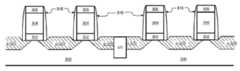
도 4a-e는 각각, 본 발명의 한 실시예에 따라 구성된 비-평면 트랜지스터 아키텍처의 투시도를 도시한다.
도 5는 본 발명의 예시적 실시예에 따른 하나 이상의 트랜지스터 구조로 구현된 컴퓨팅 시스템을 예시한다.
이해되는 바와 같이, 도면은 반드시 일정한 비율로 그려지지는 않거나, 특허청구된 발명을 도시된 특정한 구성으로 한정하고자 의도되지는 않는다. 예를 들어, 일부 도면은 일반적으로 직선, 직각, 매끄러운 표면을 나타내지만, 트랜지스터 구조의 실제 구현물은 완벽한 직선 및 직각이 아닐 수 있으며, 사용된 현실적인 가공 장비 및 기술의 제한으로, 일부 특징부는 표면 토폴로지(surface topology)를 가지거나 매끄럽지 않을 수 있다. 즉, 도면은 단지 예시적 구조를 도시하기 위해 제공된다.1A is a method of forming a transistor structure having a low contact resistance, according to an embodiment of the present invention.
Figure IB is a method of forming a transistor structure with a low contact resistance, according to another embodiment of the present invention.
2A-2F illustrate structures formed when performing the method of FIG. 1A, in accordance with an embodiment of the present invention.
Figures 3A-3C illustrate another structure formed when performing the method of Figure 1B, according to another embodiment of the present invention.
Figures 4a-e each show a perspective view of a non-planar transistor architecture constructed in accordance with one embodiment of the present invention.
Figure 5 illustrates a computing system implemented with one or more transistor structures in accordance with an exemplary embodiment of the present invention.
As will be appreciated, the drawings are not necessarily drawn to scale or are not intended to limit the claimed invention to the particular arrangements shown. For example, some drawings generally represent straight, perpendicular, smooth surfaces, but actual implementations of transistor structures may not be perfectly straight and perpendicular, and due to the limitations of the realistic processing equipment and techniques used, (surface topology) or may not be smooth. That is, the drawings are provided merely to illustrate exemplary structures.
종래 디바이스에 비해 기생 콘택 저항이 감소된 트랜지스터 디바이스를 형성하기 위한 기술이 제공된다. 이 기술은 예를 들어, 종래의 콘택 공정이 실리콘 소스/드레인 영역 바로 위에 실리사이드를 사용하고 실리콘(Si) 또는 실리콘 게르마늄(SiGe) 또는 게르마늄(Ge) 소스/드레인 영역 상의 일련의 금속과 같은 표준 콘택 스택을 이용하는 반도체 공정 흐름의 지점에서 구현될 수 있다. 일부 예시적 실시예에서, 이 기술은 CMOS 디바이스의 MOS 트랜지스터의 콘택을 구현하기 위해 사용될 수 있으며, 여기서 p-형 및 n-형 소스/드레인 영역들 및 그들의 각 콘택 금속들 사이에 III-V 반도체 재료 중간층이 제공되어 콘택 저항이 현저하게 감소된다. III-V 반도체 재료 중간층은 원하는 전도율을 제공하기 위해 작은 밴드 갭(예를 들어, 0.5 eV보다 낮음)을 가질 수 있고/있거나, 그렇지 않으면 도핑될 수 있다. 이 기술은 변형(strained) 및 비변형(unstrained) 채널 구조를 포함하는 다수의 트랜지스터 아키텍처(예를 들어, 평면형, 핀형(finned) 및 나노와이어 트랜지스터)에 대해 사용될 수 있다.A technique for forming a transistor device with reduced parasitic contact resistance compared to conventional devices is provided. This technique may be used, for example, in the case where a conventional contact process uses a silicide directly over a silicon source / drain region and a standard contact, such as a series of metals on a silicon (Si) or silicon germanium (SiGe) or germanium Lt; RTI ID = 0.0 > semiconductor < / RTI > In some exemplary embodiments, this technique can be used to implement the contacts of a MOS transistor of a CMOS device, wherein the p-type and n-type source / drain regions and their respective contact metal A material interlayer is provided to significantly reduce contact resistance. The III-V semiconductor material interlayer may have a small bandgap (e.g., less than 0.5 eV) and / or may be doped to provide a desired conductivity. This technique can be used for multiple transistor architectures (e.g., planar, finned and nanowire transistors) including strained and unstrained channel structures.
개요summary
전술한 바와 같이, 트랜지스터의 구동 전류 증가는 디바이스 저항을 감소시킴으로써 달성될 수 있다. 콘택 저항은 디바이스의 전체 저항 중 한 성분이다. 통상적인 트랜지스터 콘택 스택은, 예를 들어, 실리콘 또는 SiGe 소스/드레인 층, 실리사이드/게르마나이드 층, 티타늄 질화물 접착층, 및 텅스텐 콘택/플러그를 포함한다. 니켈, 백금, 티타늄, 코발트 등과 같은 금속의 실리사이드 또는 게르마나이드는 텅스텐 플러그 퇴적 전에 소스-드레인 영역 상에 형성될 수 있다. 그러한 구성에서, 콘택 저항은 비교적 높으며, 금속의 피닝 레벨(pinning level)에 대한 실리콘 또는 SiGe 원자가 전자대(valence band) 정렬에 의해 실질적으로 제한된다. 콘택을 형성하는 통상적인 산업적 접근은 일반적으로 밴드 갭이 0.5-1.5 eV의 범위 또는 그 이상인 합금을 사용한다. 그러한 일부 접근법은 n-형 트랜지스터 구조에 적합할 수 있지만, p-형 트랜지스터 구조에는 적합하지 않다.As described above, the driving current increase of the transistor can be achieved by reducing the device resistance. The contact resistance is one of the total resistance of the device. A typical transistor contact stack includes, for example, a silicon or SiGe source / drain layer, a silicide / germanium layer, a titanium nitride bond layer, and a tungsten contact / plug. A silicide or germanide of a metal such as nickel, platinum, titanium, cobalt, and the like may be formed on the source-drain region prior to deposition of the tungsten plug. In such a configuration, the contact resistance is relatively high and is substantially limited by the silicon or SiGe valence electron band alignment with respect to the pinning level of the metal. Conventional industrial approaches to forming contacts typically use alloys with bandgaps in the range of 0.5-1.5 eV or greater. Some such approaches may be suitable for n-type transistor structures, but are not suitable for p-type transistor structures.
따라서, 그리고 본 발명의 실시예에 따라, 소스/드레인 형성 이후에 하지만 금속 콘택 퇴적 전에, III-V 반도체 재료 중간층이 퇴적된다. p-형 및 n-형 소스/드레인 영역 모두의 위에 동일한 III-V 반도체 재료 중간층이 퇴적될 수 있음을 주목한다. 일부 실시예에서, III-V 재료 층은, 예를 들어, 알루미늄(Al), 갈륨(Ga), 인듐(In), 인(P), 비소(As) 및/또는 안티몬(Sb)의 각종 조합을 포함하는, 안티몬화 인듐(InSb), 또는 밴드 갭이 0.5 eV 미만인 다른 관련 화합물과 같이, 좁은 밴드 갭을 갖도록 선택된다. 상기 작은 밴드 갭의 III-V 재료 층은, 예를 들어, p-형 및 n-형 Si, SiGe 합금 및 Ge 소스-드레인 영역과 같은 MOS 트랜지스터 소스-드레인 영역에 우수한 콘택 특성을 제공하기 위해 사용될 수 있다. 다른 실시예에서, 임의의 밴드 갭을 갖는 III-V 재료를 퇴적 및 도핑할 수 있으며, 이로써 작은 밴드 갭의 III-V 재료에 비견할 만한 수준, 또는 주어진 응용에 대해 허용가능한 전도율 수준까지 전도율을 증가시킬 수 있다.Thus, and in accordance with an embodiment of the present invention, after the source / drain formation, but before the metal contact deposition, the III-V semiconductor material intermediate layer is deposited. It should be noted that the same III-V semiconductor material intermediate layer may be deposited on both the p-type and n-type source / drain regions. In some embodiments, the III-V material layer may be formed of any combination of, for example, aluminum (Al), gallium (Ga), indium (In), phosphorus (P), arsenic (As) Such as indium antimonide (InSb), or other related compounds having a bandgap of less than 0.5 eV. The III-V material layer of the small bandgap may be used to provide good contact properties to MOS transistor source-drain regions, such as, for example, p-type and n-type Si, SiGe alloys and Ge source- . In another embodiment, a III-V material having an arbitrary bandgap may be deposited and doped, thereby providing a level comparable to a small bandgap III-V material, or a conductivity to an acceptable conductivity level for a given application .
일부 실시예에서, III-V 반도체 재료, 및 특히 약 0.5 eV 미만의 밴드 갭을 갖는 III-V 재료는 도핑되지 않고 남아 있을 수 있으며, 이는 상기 작은 밴드 갭 재료에서 캐리어의 열 발생이 실온에서 높은 전도율을 가능하게 하기에 충분하기 때문임을 주목한다. 임의의 밴드 갭을 갖는 III-V 재료를 사용한 것과 같은, 도핑이 사용된 다른 실시예에서, 도핑은 인-시튜(in-situ) 및 엑스-시튜(ex-situ) 도핑 기술 모두를 포함하는 다수의 방식으로 수행될 수 있다. 상기 일부 실시예는, 탄소, 실리콘, 게르마늄 또는 주석과 같은 IV족 도펀트로 충분히 높은 도핑 수준을 갖는 III-V 재료를 사용한다. 매우 높은 도핑 수준에서(예를 들어, 치환 농도 1E18 atoms/cm3 초과), 상기 양쪽성 도펀트는 원자가 전자대 및 전도대 모두에서 캐리어에 기여하여, 두 캐리어 종류 모두에 대한 캐리어 농도를 증가시킨다. 상기 일부 경우에, 도핑은 인-시튜로 수행된다. 다른 실시예에서, 진성 III-V 재료 층을 퇴적한 다음, 원하는 전도율(예를 들어, 100 내지 500 S/cm의 값을 갖는 전도율)을 제공하도록, 이온 주입 또는 확산 도핑과 같은 엑스-시튜 도핑 공정이 후속한다. 일부 예시적인 경우에, p-형 영역이 제1 도핑 체계를 갖고 n-형 영역이 제2 도핑 체계를 갖도록 III-V 재료 층이 도핑될 수 있다. 예를 들어, n-형 소스/드레인 영역은 예를 들어 실리콘, 게르마늄 또는 텔루륨으로 도핑될 수 있고, p-형 소스/드레인 영역은 아연 또는 카드뮴으로 도핑될 수 있다. 본 발명의 관점에서 이해되는 바와 같이, 복수의 도핑 체계를 수반하는 상기 실시예는 일반적으로 추가 패터닝 단계를 필요로 할 것이다.In some embodiments, a III-V semiconductor material, and in particular a III-V material having a bandgap of less than about 0.5 eV, may remain undoped, which may cause the heat generation of the carrier in the small bandgap material to be high Note that this is sufficient to enable conductivity. In other embodiments where doping is used, such as using a III-V material with an arbitrary bandgap, the doping may be performed using a plurality of in-situ and ex-situ doping techniques, including both in-situ and ex- . ≪ / RTI > Some of these embodiments use III-V materials with sufficiently high doping levels as Group IV dopants such as carbon, silicon, germanium or tin. At very high doping levels (e.g., substituted concentration 1E18 atoms / cm3 greater than), the amphoteric dopant contributes to the carriers in both the conduction band and the valence electrons for, thereby increasing the carrier concentration of both carrier types. In this case, the doping is performed in-situ. In another embodiment, a layer of intrinsic III-V material is deposited and then subjected to x-dose doping, such as ion implantation or diffusion doping, to provide a desired conductivity (e.g., a conductivity having a value of 100 to 500 S / cm) Process follows. In some exemplary cases, the III-V material layer may be doped such that the p-type region has a first doping system and the n-type region has a second doping system. For example, the n-type source / drain region may be doped with, for example, silicon, germanium or tellurium, and the p-type source / drain region may be doped with zinc or cadmium. As will be appreciated in view of the present invention, such embodiments involving a plurality of doping systems will generally require additional patterning steps.
평면형, 돌출형(raised) 소스/드레인, 비-평면형(예를 들어, 이중-게이트 및 트리게이트(trigate) 트랜지스터 구조와 같은 나노와이어 트랜지스터 및 핀형(finned) 트랜지스터) 뿐만 아니라, 변형 및 비변형 채널 구조를 포함하는, 임의의 수의 트랜지스터 구조 및 구성에서 콘택 저항을 향상시키기 위해 III-V 재료 층을 사용할 수 있음을 추가로 주목한다. 또한, 트랜지스터 구조는, 예를 들어, 때때로 수행되는 것과 같이 쇼트 채널 효과(short channel effect;SCE)를 향상시키면서 트랜지스터의 총 저항을 감소시키기 위해 설계된 소스 및 드레인 단부 영역을 포함할 수 있다. 본 출원에 설명된 바와 같은 III-V 반도체 재료 층과 함께 임의의 수의 구조적 특징부를 사용할 수 있다.As well as nanowire transistors and finned transistors such as planar, raised source / drain, non-planar (e.g., double-gate and tri-gate transistor structures) 0.0 > III-V < / RTI > material layer may be used to improve the contact resistance in any number of transistor structures and configurations, including < RTI ID = 0.0 > The transistor structure may also include source and drain end regions designed to reduce the total resistance of the transistor while improving, for example, the short channel effect (SCE) as is sometimes done. Any number of structural features may be used in conjunction with a III-V semiconductor material layer as described in this application.
트랜지스터 구조는 p-형 소스/드레인 영역, n-형 소스/드레인 영역, 또는 n-형 및 p-형 소스/드레인 영역 모두를 포함할 수 있다. 일부 예시적 실시예에서, 트랜지스터 구조는 MOS 구조에 실리콘, SiGe 합금, 또는 명목상 순수 게르마늄 필름(예를 들어, 10% 미만의 실리콘을 갖는 것)의 도펀트-주입 소스/드레인 영역 또는 에피택셜(또는 다결정) 대체 소스/드레인 영역을 포함한다. 상기 임의의 구현물에서, 본 발명의 실시예에 따라, III-V 반도체 재료의 층 또는 캡(cap)은 소스/드레인 영역 바로 위에 형성될 수 있다. III-V 재료 층은 또한, 바람직할 경우, 폴리 게이트 및/또는 접지 탭(tap) 영역, 또는 낮은 콘택 저항이 원하는 영역과 같은, 트랜지스터 구조의 다른 부분 바로 위에도 형성될 수 있다.The transistor structure may include a p-type source / drain region, an n-type source / drain region, or both n-type and p-type source / drain regions. In some exemplary embodiments, the transistor structure may be doped with a dopant-implanted source / drain region or epitaxial (or alternatively doped) region of a silicon, SiGe alloy, or nominally pure germanium film (e.g., with less than 10% Polycrystalline) alternative source / drain regions. In any of the above implementations, according to embodiments of the present invention, a layer or cap of III-V semiconductor material may be formed directly above the source / drain regions. The III-V material layer may also be formed directly over other portions of the transistor structure, such as a poly gate and / or a ground tap region, or a low contact resistance desired region.
분석(예를 들어, 주사 전자 현미경 및/또는 조성 매핑(mapping))시, 본 발명의 조성의 실시예에 따라 구성된 구조는, 예를 들어 Al, Ga, In, P, As 및/또는 Sb의 조합을 포함하는(적용가능할 경우, 허용가능한 수준까지 전도율을 증가시키는 임의의 도펀트와 함께) III-V 반도체 재료의 추가 층을 실질적으로 도시할 것이며, 종래의 실리사이드 및 게르마나이드 콘택 공정을 이용하여 제조된 디바이스의 콘택 저항보다 더 낮은 콘택 저항을 나타낼 것이다. 이해되는 바와 같이, 고성능 콘택에 대한 요구를 갖는 임의의 수의 반도체 디바이스 또는 회로는 본 출원에 제공된 저 저항 콘택 기술로부터 이득을 얻을 수 있다.In an analysis (e.g., scanning electron microscopy and / or composition mapping), a structure constructed according to an embodiment of the composition of the present invention may include, for example, Al, Ga, In, P, As, and / V semiconductor material (with optional dopants that increase the conductivity to an acceptable level, where applicable), and may be fabricated using conventional silicide and germanium contact processes Will exhibit a contact resistance that is lower than the contact resistance of the fabricated device. As will be appreciated, any number of semiconductor devices or circuits having a demand for high performance contacts can benefit from the low resistance contact technology provided in this application.
따라서, 본 발명의 실시예에 따라 구성된 트랜지스터 구조는 종래의 구조에 비해 더 낮은 콘택 저항에 관련하여 개선을 제공한다. 본 발명의 관점에서 다수의 공정 변형이 명백할 것이다. 예를 들어, III-V 반도체 재료는 절연체 층이 소스/드레인 층 위에 퇴적되기 전에 소스-드레인 영역 상에 퇴적될 수 있다. 대안적으로, III-V 반도체 재료는 절연체 층이 소스/드레인 층 영역 위에 퇴적되고 콘택 트랜치가 소스/드레인 층까지 식각된 후에 소스-드레인 영역 상에 퇴적될 수 있다.Thus, a transistor structure constructed in accordance with an embodiment of the present invention provides an improvement with respect to lower contact resistance compared to conventional structures. Many process variations will be apparent in light of the present invention. For example, the III-V semiconductor material may be deposited on the source-drain region before the insulator layer is deposited over the source / drain layer. Alternatively, the III-V semiconductor material may be deposited on the source-drain region after the insulator layer is deposited over the source / drain layer region and the contact trench is etched to the source / drain layer.
방법론 및 아키텍처Methodology and architecture
도 1a는 본 발명의 실시예에 따라 낮은 콘택 저항을 갖는 트랜지스터 구조를 형성하는 방법이다. 도 2a 내지 2f는 상기 방법이 수행됨에 따라, 그리고 일부 실시예에 따라 형성된 예시적 구조를 예시한다.1A is a method of forming a transistor structure having a low contact resistance in accordance with an embodiment of the present invention. Figures 2a-2f illustrate exemplary structures formed as the method is performed and in accordance with some embodiments.
예시적 방법은 MOS 디바이스가 위에 형성될 수 있는 반도체 기판상에 하나 이상의 게이트 스택을 형성하는 단계(102)를 포함한다. MOS 디바이스는 NMOS 또는 PMOS 트랜지스터, 또는 NMOS 및 PMOS 트랜지스터 모두(예를 들어, CMOS 디바이스용)를 포함할 수 있다. 도 2a는 예시의 결과적인 구조를 도시하며, 이 경우에 이는 동일한 기판(300) 상에 형성되며 얕은 트랜치 분리(shallow trench isolation;STI)에 의해 분리된 NMOS 및 PMOS 트랜지스터 모두를 포함한다. p-형 및 n-형 영역 사이에 다른 적절한 형태의 분리도 또한 사용될 수 있다. 볼 수 있는 바와 같이, 각 게이트 스택은 트랜지스터의 채널 영역 위에 형성되며 게이트 유전체 층(302), 게이트 전극(304), 선택적 하드마스크(306)를 포함하며, 스페이서(310)는 게이트 스택에 인접하여 형성된다.The exemplary method includes forming (102) at least one gate stack on a semiconductor substrate on which a MOS device may be formed. A MOS device may include NMOS or PMOS transistors, or both NMOS and PMOS transistors (e.g., for CMOS devices). FIG. 2A illustrates the resulting structure of the example, which in this case includes both NMOS and PMOS transistors formed on the
게이트 유전체(302)는, 예를 들어, 실리콘 이산화물(SiO2) 또는 고-유전율(high-k) 게이트 유전체 재료와 같은 임의의 적절한 산화물일 수 있다. 고-유전율 게이트 유전체 재료의 예는, 예를 들어, 하프늄 산화물, 하프늄 실리콘 산화물, 란타늄 산화물, 란타늄 알루미늄 산화물, 지르코늄 산화물, 지르코늄 실리콘 산화물, 탄탈륨 산화물, 티타늄 산화물, 바륨 스트론튬 티타늄 산화물, 바륨 티타늄 산화물, 스트론튬 티타늄 산화물, 이트륨 산화물, 알루미늄 산화물, 납 스칸듐 탄탈륨 산화물, 및 납 아연 니오베이트를 포함한다. 일부 실시예에서, 고-유전율 재료가 사용된 경우 품질을 향상시키기 위해 게이트 유전체 층(302)상에 어닐링 공정을 수행할 수 있다. 일부 특정한 예시적 실시예에서, 고-유전율 게이트 유전체 층(302)은 두께가 5 Å 내지 약 100 Å 범위(예를 들어, 10 Å)일 수 있다. 다른 실시예에서, 게이트 유전체 층(302)은 산화물 재료의 한 단분자 층(monolayer)의 두께를 가질 수 있다. 일반적으로, 게이트 유전체(302)의 두께는 소스 및 드레인 콘택으로부터 게이트 전극(304)을 전기적으로 분리하기에 충분해야 한다. 일부 실시예에서, 고-유전율 재료의 품질을 향상시키기 위해 고-유전율 게이트 유전체 층(302)상에 어닐링 공정과 같은 추가 공정을 수행할 수 있다.Gate dielectric 302, for example, silicon dioxide (SiO2) or a high-dielectric constant may be any suitable oxide, such as the (high-k) gate dielectric material. Examples of high-permittivity gate dielectric materials include, for example, hafnium oxide, hafnium silicon oxide, lanthanum oxide, lanthanum aluminum oxide, zirconium oxide, zirconium silicon oxide, tantalum oxide, titanium oxide, barium strontium titanium oxide, barium titanium oxide, Strontium titanium oxide, yttrium oxide, aluminum oxide, lead scandium tantalum oxide, and lead zinc niobate. In some embodiments, an annealing process may be performed on the gate
게이트 전극(304)은, 비록 다른 적절한 게이트 전극 재료도 또한 사용될 수 있기는 하지만, 예를 들어 폴리실리콘, 실리콘 질화물, 실리콘 탄화물 또는 금속 층(예를 들어, 텅스텐, 티타늄 질화물, 탄탈륨, 탄탈륨 질화물)일 수 있다. 게이트 전극(304) 재료는, 대체 금속 게이트(replacement metal gate;RMG) 공정을 위해 이후에 제거되는 희생 재료일 수 있으며, 일부 예시적 실시예에서 두께가 10 Å 내지 500 Å의 범위(예를 들어, 100 Å)를 갖는다.The
선택적 게이트 하드 마스크 층(306)은 이후의 식각 및/또는 이온주입 공정으로부터 게이트 전극(304)을 보호하는 것과 같은, 공정 동안의 특정 장점 또는 용도를 제공하기 위해 사용될 수 있다. 하드 마스크 층(306)은 실리콘 이산화물, 실리콘 질화물 및/또는 다른 종래의 절연체 재료와 같은 통상적인 하드 마스크 재료를 이용하여 형성될 수 있다.The optional
게이트 스택은 종래에 수행되는 바와 같이 또는 임의의 적절한 관습적 기술(예를 들어, 도 2a에 도시된 바와 같은, 게이트 전극 및 게이트 유전체 층의 일부를 식각해 내어 게이트 스택을 형성하는 종래의 패터닝 공정)을 이용하여 형성될 수 있다. 게이트 유전체(302) 및 게이트 전극(304) 재료는 각각, 예를 들어 CVD(chemical vapor deposition), ALD(atomic layer deposition), SOD(spin-on deposition) 또는 PVD(physical vapor deposition)과 같은 종래의 퇴적 공정을 이용하여 형성될 수 있다. 다른 퇴적 기술도 또한 사용될 수 있으며, 예를 들어 게이트 유전체(302) 및 게이트 전극(304) 재료를 열 성장시킬 수 있다. 본 발명의 관점에서 이해되는 바와 같이, 본 출원에 설명된 낮은 콘택 저항 트랜지스터 디바이스 또는 구조를 제공하도록, 임의의 수의 다른 적절한 재료, 기하학적 구조 및 형성 공정을 이용하여 본 발명의 실시예를 구현할 수 있다.The gate stack may be formed by a conventional patterning process, such as is performed conventionally, or by any suitable conventional technique (e.g., as shown in FIG. 2A, to etch portions of the gate electrode and gate dielectric layer to form a gate stack) ). ≪ / RTI > The
스페이서(310)는, 예를 들어 실리콘 산화물, 실리콘 질화물 또는 다른 적절한 스페이서 재료와 같은 종래의 재료를 이용하여 형성될 수 있다. 스페이서(310)의 폭은 형성되는 트랜지스터에 대한 설계 요건을 기초로 일반적으로 선택될 수 있다. 하지만, 일부 실시예에 따라, 소스/드레인 단부 영역의 붕소 도핑 게르마늄 함량이 충분히 높을 경우, 스페이서(310)의 폭에는 소스 및 드레인 에피-단부의 형성에 의해 부과된 설계 제한이 적용되지 않는다.
이후의 게이트 패터닝 공정 전에 핀(fins) 또는 나노와이어가 위에 형성된 기판을 포함하여, 벌크 기판, 반도체-온-절연체 기판(semiconductors-on-insulator;XOI, 여기서 X는 실리콘, 게르마늄, 또는 게르마늄-풍부 실리콘과 같은 반도체 재료임), 및 다중 층 구조를 포함하는 임의의 수의 적절한 기판을 사용하여 기판(300)을 구현할 수 있다. 일부 특정 예시적 경우에, 기판(300)은 게르마늄 또는 실리콘 또는 SiGe 벌크 기판, 또는 산화물 기판상의 게르마늄 또는 실리콘 또는 SiGe이다. 비록 기판(300)이 형성될 수 있는 재료의 몇 가지 예가 여기서 설명되지만, 낮은 콘택 저항 반도체 디바이스가 위에 구축될 수 있는 토대로서 작용할 수 있는 임의의 재료가 특허청구된 발명의 사상 및 범위 내에 속한다.A semiconductor substrate, such as a bulk substrate, a semiconductors-on-insulator (XOI), where X is silicon, germanium, or a germanium-rich substrate, including fins or nanowires formed thereon before the subsequent gate patterning process (E.g., a semiconductor material such as silicon), and any number of suitable substrates including multilayered structures. In some specific illustrative cases, the
도 1a를 추가로 참조하여, 하나 이상의 게이트 스택이 형성된 후에, 방법은 계속해서 트랜지스터 구조의 소스/드레인 영역을 정의한다(104). 소스/드레인 영역은 임의의 수의 적절한 공정 및 구성으로 구현될 수 있다. 예를 들어, 소스/드레인 영역은 이온주입되고, 식각되고 에피-충전된, 돌출된, 실리콘 또는 게르마늄 또는 SiGe 합금, p-형 및/또는 n-형일 수 있으며, 평면형 또는 핀형 또는 와이어형 확산 영역을 가질 수 있다. 예를 들어, 상기 일부 예시적 경우에, 소스 및 드레인 영역은 이온주입/확산 공정 또는 식각/퇴적 공정 중 하나를 이용하여 형성될 수 있다. 전자의 공정에서, 붕소, 알루미늄, 안티몬, 인 또는 비소와 같은 도펀트를 기판(300)에 이온주입하여 소스 및 드레인 영역을 형성할 수 있다. 이온주입 공정에는 통상적으로, 도펀트를 활성화하고 이들을 또한 기판(300)에 추가로 확산시키도록 유발할 수 있는 어닐링 공정이 후속한다. 후자의 공정에서, 기판(300)을 먼저 식각하여 소스 및 드레인 영역의 위치에 오목부(recess)를 형성할 수 있다. 이어서, 에피택셜 퇴적 공정을 수행하여 실리콘 게르마늄 또는 실리콘 탄화물과 같은 실리콘 합금으로 오목부를 충전할 수 있고, 이로써 소스 및 드레인 영역을 형성할 수 있다. 일부 구현에서, 에피택셜 퇴적된 실리콘 합금을 붕소, 비소 또는 인과 같은 도펀트로 인-시튜 또는 엑스-시튜 도핑할 수 있다.With further reference to FIG. 1A, after one or more gate stacks are formed, the method continues to define the source / drain regions of the transistor structure (104). The source / drain regions may be implemented in any number of suitable processes and configurations. For example, the source / drain regions may be ion implanted, etched and epi-filled, protruding, silicon or germanium or SiGe alloys, p-type and / or n- Lt; / RTI > For example, in some of the above illustrative cases, the source and drain regions may be formed using either an ion implantation / diffusion process or an etching / deposition process. In the former process, a dopant such as boron, aluminum, antimony, phosphorus, or arsenic may be implanted into the
도 2a-2f에 도시된 예시적 실시예에서, 캐비티 뿐만 아니라, 게이트 유전체(302)를 언더컷(undercut)하는 각 단부 영역을 제공하도록 기판(300)을 식각하였다. 캐비티 및 단부 영역을 충전하여 소스/드레인 영역 및 선택적 단부 영역을 제공하였다. 기판(300)이 실리콘 벌크 또는 실리콘-온-절연체(SOI) 기판인 일부 특정 예시적 실시예에 따라, 그들의 각 단부 영역과 함께 소스 및 드레인 캐비티를 인-시튜 도핑된 실리콘 또는 SiGe 또는 게르마늄으로 충전하여 소스 및 드레인 영역(그들의 각 에피-단부와 함께)을 형성한다. 여기서, 재료(예를 들어, 도핑 또는 비도핑 Si, Ge, SiGe), 도펀트(예를 들어, 붕소, 비소 또는 인) 및 기하학적 구조(예를 들어, 소스/드레인 층의 두께는 동일 평면이거나 돌출된 소스/드레인 영역을 제공하도록, 예를 들어 50 내지 500 nm의 범위일 수 있음)와 관련하여 임의의 수의 소스/드레인 층 구성을 사용할 수 있다.In the exemplary embodiment shown in Figures 2A-2F, the
본 발명의 관점에서 이해되는 바와 같이, 본 발명의 실시예를 이용하여 임의의 수의 다른 트랜지스터 특징부를 구현할 수 있다. 예를 들어, 채널은 변형되거나 변형되지 않을 수 있으며, 소스/드레인 영역은 상응하는 소스/드레인 영역과 채널 영역 사이의 영역에 형성된 단부 영역을 포함할 수 있거나 포함하지 않을 수 있다. 이런 의미에서, 트랜지스터 구조가 변형 또는 비변형 채널을 갖는지 여부, 또는 소스-드레인 단부 영역을 갖는지 또는 소스-드레인 단부 영역을 갖지 않는지 여부는 본 발명의 각종 실시예와 특별히 관련 없으며, 상기 실시예가 임의의 특정한 상기 구조적 특징으로 한정되는 것을 의도하지 않는다. 오히려, 임의의 수의 트랜지스터 구조 및 종류, 및 특히 n-형 및 p-형 소스/드레인 트랜지스터 영역 모두를 갖는 이들 구조가, 본 출원에 설명된 바와 같이 소스/드레인 영역 위에 작은 밴드 갭의 및/또는 그렇지 않으면 충분히 도핑된 III-V 재료 층을 사용함으로써 이득을 취할 수 있다. 일반적으로, 밴드 갭이 충분히 작을 경우, 실온에서 도펀트가 필요하지 않다(비록 바람직할 경우 도펀트를 사용할 수 있기는 하지만). 한 특정한 예시적 경우에, InSb는 도핑되지 않은 p-형 및 n-형 소스/드레인 영역 모두에 제공된다. 더 큰 밴드 갭의 III-V 재료(>0.5 eV)에 있어서, 원하는 전도율을 제공하기 위해 도핑을 사용할 수 있다.As will be appreciated in view of the present invention, any number of other transistor features may be implemented using embodiments of the present invention. For example, the channel may be strained or unmodified, and the source / drain region may or may not include an end region formed in the region between the corresponding source / drain region and the channel region. In this sense, whether or not the transistor structure has a strained or unstrained channel, or whether it has a source-drain end region or a source-drain end region, is not specifically related to various embodiments of the present invention, And is not intended to be limited to the particular structural features described above. Rather, any number of transistor structures and types, and especially those structures with both n-type and p-type source / drain transistor regions, can be fabricated with a small bandgap over the source / drain regions and / Or otherwise can benefit from using a fully doped III-V material layer. In general, if the bandgap is sufficiently small, a dopant is not needed at room temperature (although a dopant can be used if desired). In one particular illustrative case, InSb is provided in both undoped p-type and n-type source / drain regions. For III-V materials (> 0.5 eV) of a larger bandgap, doping can be used to provide the desired conductivity.
도 1a를 추가로 참고하여, 소스/드레인 영역이 정의된 후, 이 예시적 실시예의 방법은 계속하여 절연체 층(322)을 퇴적한다(106). 도 2b는 절연체 층(322)이 게이트 스택의 하드 마스크(306)와 동일 높이인 것으로 도시하지만, 그럴 필요는 없다. 절연체는 다수의 방식으로 구성될 수 있다. 일부 실시예에서, 절연체 층(322)은 SiO2 또는 다른 저-유전율 절연체 재료로 구현된다. 더 일반적인 의미에서, 층(322) 재료의 유전율은 원하는 대로 선택될 수 있다. 일부 실시예에서, 절연체 층(322)은 라이너(예를 들어, 실리콘 질화물)에 후속하여, SiO2, 또는 질화물, 산화물, 산질화물, 탄화물, 옥시탄화물(oxycarbide), 또는 다른 적절한 절연체 재료의 임의의 조합의 하나 이상의 층을 포함할 수 있다. 층간 유전체(interlayer dielectric;ILD)로 지칭될 수 있는 절연체 층(322)은 통상적으로 수행되는 바와 같이(예를 들어, CMP(chemical mechanical planarization)와 같은 후-퇴적 평탄화에 의해) 평탄화될 수 있다. 층(322)을 형성하기 위해 사용될 수 있는 다른 예시적 절연체 재료는, 예를 들어 탄소 도핑 산화물(carbon doped oxide;CDO), 퍼플루오로시클로부탄 또는 폴리테트라플루오로에틸렌과 같은 유기 고분자, 플루오로실리케이트 유리(fluorosilicate glass;FSG), 및 실세스퀴옥산, 실록산 또는 유기실리케이트 유리와 같은 유기실리케이트를 포함한다. 일부 예시적 구성에서, 절연체 층(322)은 유전율을 더 감소시키기 위해 기공(pores) 또는 다른 보이드(voids)를 포함할 수 있다.With additional reference to FIG. 1A, after the source / drain regions are defined, the method of this exemplary embodiment continues to deposit (106) the
본 발명의 관점에서 이해되는 바와 같이, 그리고 대체 금속 게이트(RMG) 공정이 사용된 본 발명의 일부 실시예에 따라, 방법은 종래에 수행되는 바와 같이 식각 공정을 이용하여 게이트 스택(고-유전율 게이트 유전체 층(302), 희생 게이트 전극(304), 및 하드 마스크 층(306)을 포함함)을 제거하는 단계를 추가로 포함할 수 있다. 상기 일부 경우에, 희생 게이트(304) 및 하드 마스크 층(306) 만이 제거된다. 게이트 유전체 층(302)이 제거된 경우, 방법은 계속해서 트랜치 개구부에 새로운 게이트 유전체 층을 퇴적할 수 있다. 하프늄 산화물과 같은, 전술된 바와 같은 임의의 적절한 게이트 유전체 재료를 여기서 사용할 수 있다. 동일한 퇴적 공정도 또한 사용할 수 있다. 예를 들어, 건식 및 습식 식각 공정의 적용 동안 원래의 게이트 유전체 층에 발생할 수 있는 임의의 손상을 다루기 위해, 및/또는 저-유전율 또는 희생 유전체 재료를 고-유전율 또는 다른 원하는 게이트 유전체 재료로 대체하기 위해 게이트 유전체 층의 대체물을 사용할 수 있다. 상기 RMG 공정에서, 방법은 트랜치 내에 및 게이트 유전체 층 위에 게이트 전극 층을 퇴적하는 단계를 추가로 포함할 수 있다. 대체 게이트 전극을 형성하기 위해 CVD, ALD 및 PVD와 같은 종래의 퇴적 공정을 사용할 수 있다. 게이트 전극 층은, 예를 들어, 루테늄, 팔라듐, 백금, 코발트, 니켈, 및 예를 들어 루테늄 산화물인 전도성 금속 산화물과 같은, p-형 일함수 금속을 포함할 수 있다. 일부 예시적 구성에서, 2개 이상의 금속 게이트 전극 층을 퇴적할 수 있다. 예를 들어, 게이트 트랜치에 일함수 금속을 퇴적한 다음, 알루미늄 또는 은과 같은 적절한 금속 게이트 전극 충전 금속을 퇴적할 수 있다. 도 2b'는 상기 선택적 RMG 공정으로부터 결과적인 예시적 게이트 구조를 도시하며, 이는 대체 게이트 유전체 층(324) 위에 대체 게이트 전극 층(326)을 포함한다. 또 다른 실시예에서, 상기 RMG 공정은, 대체 게이트 재료에 단계 108 내지 114와 관련된 공정이 수행되지 않도록, 방법의 후반에(예를 들어, 단계 114 이후에) 수행될 수 있다.As will be appreciated in view of the present invention, and in accordance with some embodiments of the present invention in which an alternate metal gate (RMG) process is used, the method may use an etch process to form a gate stack (Including
도 1a를 추가로 참조하여, 절연체 층(322)이 제공된(및 임의의 원하는 예비-콘택 형성 RMG 공정) 이후에, 방법은 계속해서 식각하여 소스/드레인 콘택 트랜치를 형성한다(108). 임의의 적절한 건식 및/또는 습식 식각 공정을 사용할 수 있다. 도 2c는 한 예시적 실시예에 따른, 식각이 완료된 후의 소스/드레인 콘택 트랜치를 도시한다.1A, after the
방법은 계속해서 트랜지스터 구조의 소스/드레인 영역 상에 III-V 반도체 재료 층을 퇴적한다(110). 도 2d는 한 예시적 실시예에 따른, n-형 및 p-형 소스/드레인 영역 모두 위의 III-V 재료 층(317)을 도시한다. 상기 퇴적은 비-선택적으로 수행될 수 있으며, 여기서 임의의 과량의 III-V 퇴적물은 이후에 절연체(322)(및 필요할 경우 게이트 스택)의 상부로부터 제거된다. 다른 실시예에서, 퇴적은 선택적으로 수행될 수 있으며, 여기서 III-V 재료 퇴적물은 소스/드레인 영역(또는 그의 하위 세트(sub-set))에만 존재한다. 예를 들어, 일부 예시적 실시예에서, 공정이, p-형 영역 또는 n-형 영역을 마스킹한 다음 선택적으로 퇴적하여 한 영역 또는 다른 영역에서 고유하게 퇴적을 달성(예를 들어, 여기서 p-형 영역은 제1 도핑 체계를 갖는 III-V 재료 화합물을 수용하고, n-형 영역은 제2 도핑 체계를 갖는 III-V 재료 화합물을 수용함)하는 단계를 포함한다는 점에서 퇴적(110)은 선택적이다. 대안적으로, 퇴적(110)은, 모든 소스/드레인 영역 상에서 비도핑 III-V 재료의 단일 조성물로 이루어질 수 있으며, 이후의 마스킹 및 도핑이 후속하여, 아래의 소스/드레인 재료의 도핑 종류에 대한 콘택 저항을 추가로 최적화할 수 있다. 대안적으로, 퇴적(110)은, 모든 소스/드레인 영역 상에서 비도핑 III-V 재료의 단일 조성물로 이루어질 수 있으며, 여기서 비도핑 III-V 재료는 0.5 eV 미만의 밴드 갭을 갖는다(예를 들어, InxGa1-xAs의 밴드 갭=0.427 eV, 여기서 x=0.9임). 상기 일부 작은 밴드 갭의 경우에, 밴드 갭은 0.4 eV 미만이다(예를 들어, InAs의 밴드 갭=0.36 eV). 또 다른 상기 경우에, 밴드 갭은 0.3 eV 미만이다. 또 다른 상기 경우에, 밴드 갭은 0.2 eV 미만이다(예를 들어, InSb의 밴드 갭=0.17 eV). 또 다른 상기 경우에, 밴드 갭은, 예를 들어 0.1 eV와 0.4 eV 사이, 또는 0.1 eV와 0.25 eV 사이, 또는 0.25 eV와 0.5 eV 사이, 또는 0.15 eV와 0.35 eV 사이와 같은 범위 이내이다. 하지만, III-V 재료는 0.5 eV 미만의 밴드 갭을 갖는 것으로 제한될 필요가 없음을 주목한다. 이는, III-V 재료가 아래의 소스/드레인 재료의 도핑 종류에 맞춰지도록, 예를 들어 인-시튜 도핑, 확산 도핑, 또는 이온주입 도핑으로 퇴적될 수 있기 때문이다.The method subsequently deposits a layer of III-V semiconductor material (110) on the source / drain regions of the transistor structure. 2D illustrates a III-
일부 예시적 실시예에서, III-V 재료 층(317)은 에피택셜 퇴적된다. 본 발명의 관점에서 명백한 바와 같이, III-V 재료 층(317)의 두께는, 비록 다른 실시예는 다른 층 두께를 가질 수 있기는 하지만, 일부 특정 예시적 실시예에 따라, 예를 들어 50 내지 250 Å 범위일 수 있다. 일부 실시예에서, III-V 재료 층(317)의 퇴적(110) 또는 형성을 위해 CVD 공정 또는 다른 적절한 퇴적 기술을 사용할 수 있다. 예를 들어, 퇴적(110)은, Al, Ga, In, P, As, Sb 및/또는 그의 전구체의 조합과 같은 III-V 재료 화합물을 이용하여 CVD 또는 RT-CVD(rapid thermal CVD) 또는 LP-CVD(low pressure CVD) 또는 UHV-CVD(ultra-high vaccum CVD) 또는 GS-MBE(gas source molecular beam epitaxy) 장치에서 수행될 수 있다. 하나의 특정한 상기 예시적 실시예에서, III-V 재료 층(317)은 비도핑 안티몬화 인듐(InSb)으로 구현된다. 다른 실시예에서, III-V 재료 층(317)은 1E19 atom/cm3 이상의 Ge 치환 농도를 제공하도록 Ge로 도핑된 GaAs로 구현되며, 이는 약 5E-3 Ohm-cm의 저항률(또는 약 200 Mho/cm의 상응하는 전도율)을 초래한다. 임의의 상기 실시예에서, 예를 들어 수소, 질소 또는 비활성 기체(noble gas)와 같은 캐리어 기체가 존재할 수 있다(예를 들어, 전구체는 나머지가 캐리어 기체인 1-20% 농도로 희석된다). 일부 예시적 경우에, 아르신(arsine) 또는 TBA와 같은 아르신 전구체, TMG와 같은 갈륨 전구체, 및/또는 TMI와 같은 인듐 전구체가 존재할 수 있다. 예를 들어, 염화 수소(HCl), 염소(Cl) 또는 브롬화 수소(HBr)와 같은 할로겐계 기체와 같은 식각제 기체도 또한 존재할 수 있다. 예를 들어 300 ℃ 내지 700 ℃의 범위(예를 들어, 400-500 ℃)의 퇴적 온도 및 예를 들어 1 Torr 내지 760 Torr의 범위의 반응기 압력을 이용한 광범위한 조건에 걸쳐 III-V 반도체 재료 층(317)의 기본 퇴적이 가능하다. 캐리어 및 식각제는 각각 10과 300 SCCM 범위의 유량(flow)을 가질 수 있다(통상적으로, 100 SCCM 이하의 유량이 요구되지만, 일부 실시예는 더 높은 유속(flow rate)이 유리할 수 있다). 한 특정한 예시적 실시예에서, 퇴적(110)은 100과 1000 SCCM 사이의 범위인 유속으로 수행된다. 게르마늄의 인-시튜 도핑을 위해, 예를 들어 희석 게르만(germane) 또는 다이게르만(digermane)을 사용할 수 있다(예를 들어, 게르만은 10% 농도 및 10과 100 sccm 사이의 범위인 유속으로 H2에 희석될 수 있음).In some exemplary embodiments, the III-
본 발명의 관점에서 이해되는 바와 같이, III-V 재료 층(317)이 퇴적되는 선택도(selectivity)는 원하는 대로 변경될 수 있다. 일부 경우에, 예를 들어, III-V 재료 층(317)은 소스/드레인 영역 상에만 또는 소스/드레인 영역의 일부(전체 구조에 걸쳐서가 아니라) 상에만 퇴적된다. 하위 세트 영역을 추가로 정의하는 임의의 수의 마스킹/패터닝 기술을 사용하여 층(317)을 선택적으로 퇴적할 수 있다. 또한, 예를 들어 층(317)이, 노출된 폴리 게이트 영역 또는 노출된 접지 탭 영역을 덮는 다른 실시예가 유리할 수 있다. 본 발명의 관점에서 추가로 이해되는 바와 같이, 일부 예시적 실시예에 따라, 소스 및 드레인 영역(및 접지 탭 영역과 같이 낮은 콘택 저항이 원하는 다른 영역)에서 상당히 더 낮은 콘택 저항을 실현하기 위해 III-V 재료 층(317)을 사용할 수 있다.As will be appreciated in view of the present invention, the selectivity with which the III-
이어서, 방법은 계속해서 콘택 저항 감소 금속을 퇴적하고 어닐링한(112) 다음, 소스/드레인 콘택 플러그를 퇴적한다(114). 그러한 실시예에서 실리사이드 또는 게르마나이드가 존재하지 않음을 주목한다. 오히려, III-V 재료(317)와 금속성 콘택 저항 감소 층(325) 사이에 임의의 반응이 존재한다. 도 2e는 콘택 저항 감소 금속(325)을 도시하며, 이는 일부 실시예에서 은, 니켈, 알루미늄, 티타늄, 금, 금-게르마늄, 니켈-백금 또는 니켈-알루미늄 및/또는 다른 그러한 저항 감소 금속 또는 합금을 포함한다. 다른 실시예는 바람직할 경우 층(317)과 층(325) 사이의 접착층과 같은 추가 층들을 추가로 포함할 수 있다. 도 2f는 콘택 플러그 금속(329)을 도시하며, 이는, 비록 종래의 퇴적 공정을 이용하여 은, 니켈-백금 또는 니켈-알루미늄 또는 니켈 및 알루미늄의 다른 합금, 또는 티타늄과 같은 임의의 적절한 전도성 콘택 금속 또는 합금이 사용될 수 있기는 하지만, 일부 실시예에서 알루미늄 또는 텅스텐을 포함한다. 일부 예시적 경우에, 소스/드레인 영역과 콘택 저항 감소 금속(325) 사이의 계면에 III-V 재료 층(317)으로 구성된 소스/드레인을 갖는 트랜지스터는 100 Ohm-㎛ 미만의 저항률 값을 나타낼 수 있으며, 일부 경우에, 90 Ohm-㎛ 미만, 및 일부 경우에 80 Ohm-㎛ 미만, 및 일부 경우에 75 Ohm-㎛ 미만, 또는 그 이하의 저항률 값을 나타낼 수 있다.Next, the method continues with depositing and annealing the contact resistance reducing metal (112) and depositing (114) the source / drain contact plug. Note that no silicide or germanide is present in such an embodiment. Rather, there is an arbitrary reaction between the III-
도 1b는 본 발명의 다른 실시예에 따른, 낮은 콘택 저항을 갖는 트랜지스터 구조를 형성하는 방법이다. 도 3a 내지 3c는 형성된 다른 예시적 구조를 예시한다. 일반적으로, 상기 방법은, 소스/드레인 영역 상의 III-V 재료 층(317)의 퇴적이 절연체(322) 퇴적 전에 수행되는 점을 제외하고는, 도 1a 및 2a-f를 참조로 설명된 방법과 유사하다. 이는 게르마늄 재료 퇴적 단계(110)를, 소스/드레인 정의 단계(104) 이후 및 절연체 퇴적 단계(106) 이전이 되도록 이동시킴으로써 도 1b에 실질적으로 도시된다. 절연체 퇴적 단계(106) 이후의 상기 결과적인 구조가 도 3a에 도시된다. 상기 예시적 실시예에서 III-V 재료 층(317)이 콘택 트랜치에 의해 노출된 부분뿐만 아니라 도시된 각 소스/드레인 영역을 어떻게 전체적으로 덮는지를 주목한다(도 2d에 최적으로 도시된 바와 같음). 도 3b는 단계 108에서 콘택 트랜치가 식각된 후의 결과적인 구조를 도시하며, 도 3c는 단계 112 및 114에서 각각 콘택 저항 감소 금속(325) 및 금속 콘택 플러그(329)가 퇴적된 후에 결과적인 구조를 도시한다. 이해되는 바와 같이, 도 1a를 참조로 논의된 예시적 방법의 유사한 부분에 대한 이전의 관련 논의가 동일하게 여기서도 적용가능하다.Figure IB is a method of forming a transistor structure with low contact resistance, according to another embodiment of the present invention. Figures 3A-3C illustrate another exemplary structure formed. Generally, the method is similar to the method described with reference to Figures 1A and 2a-f, except that the deposition of the III-
비-평면 구성Non-Planar Configuration
예를 들어 FinFET 또는 나노와이어 구성을 이용하여 비-평면 아키텍처가 구현될 수 있다. FinFET는 반도체 재료의 얇은 스트립(일반적으로 핀(fin)으로 지칭됨) 주변에 구축된 트랜지스터이다. 트랜지스터는 게이트, 게이트 유전체, 소스 영역 및 드레인 영역을 포함하는 표준 전계 효과 트랜지스터(FET) 노드(nodes)를 포함한다. 디바이스의 전도성 채널은 게이트 유전체 아래의 핀의 외측 상/내에 있다. 구체적으로, 전류는 핀의 측벽(기판 표면에 수직인 면)뿐만 아니라 핀의 상부(기판 표면에 평행한 면) 모두를 따라 흐른다. 상기 구성의 전도성 채널은 필수적으로 핀의 3개의 상이한 외부 평면 영역을 따라 존재하므로, 상기 FinFET 설계는 때로 트리-게이트 FinFET로 지칭된다. 소위 이중-게이트 FinFET와 같은 다른 종류의 FinFET 구성도 또한 가능하며, 여기서 전도성 채널은 주로 핀의 2개의 측벽만을 따라(그리고 핀의 상부는 따르지 않고) 존재한다. 나노와이어 트랜지스터(때로는 게이트-올-어라운드(gate-all-around) FET로 지칭됨)는 매우 유사하게 구성되지만, 핀 대신에 나노와이어(예를 들어, 실리콘 또는 SiGe 또는 Ge 나노와이어)가 사용되며, 게이트 재료는 일반적으로 모든 측 상에서 채널 영역을 둘러싼다. 특정 설계에 따라, 나노와이어 트랜지스터는 예를 들어 4개의 유효 게이트를 갖는다.For example, a non-planar architecture can be implemented using FinFET or nanowire configurations. A FinFET is a transistor built around a thin strip of semiconductor material (commonly referred to as a fin). The transistor includes standard field effect transistor (FET) nodes including a gate, a gate dielectric, a source region and a drain region. The conductive channel of the device is on / outside the pin below the gate dielectric. Specifically, the current flows along both the side wall of the fin (plane perpendicular to the substrate surface) as well as the top of the fin (plane parallel to the substrate surface). The FinFET design is sometimes referred to as a tri-gate FinFET, since the conductive channel of the above configuration is essentially along three different outer planar regions of the fin. Other types of FinFET configurations, such as so-called dual-gate FinFETs, are also possible, wherein the conductive channel is mainly present along two sidewalls of the fin (and not along the top of the fin). Although nanowire transistors (sometimes referred to as gate-all-around FETs) are very similar in construction, nanowires (e.g., silicon or SiGe or Ge nanowires) are used instead of pins , The gate material generally surrounds the channel region on all sides. Depending on the particular design, the nanowire transistor has, for example, four effective gates.
도 4a-4e는 각각, 본 발명의 한 실시예에 따라 구성된 예시적 비-평면 아키텍처의 투시도를 도시한다. 구체적으로, 도 4a-b는 각각 FinFET 트랜지스터 구조의 투시도를 도시하고, 도 4c-e는 예시적 나노와이어 채널 트랜지스터 구조를 도시한다. 이제 각 도면을 차례대로 설명할 것이다.Figures 4A-4E each show a perspective view of an exemplary non-planar architecture configured in accordance with one embodiment of the present invention. Specifically, Figures 4a-b each show a perspective view of a FinFET transistor structure, and Figures 4c-e show an exemplary nanowire channel transistor structure. I will now explain each drawing in turn.
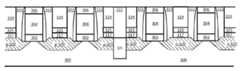
볼 수 있는 바와 같이, 도 4a에 도시된 예시적 비-평면 구성은, 각각 분리 영역(620)을 통해 기판(600)으로부터 연장된 반도체 바디 또는 핀(660)을 갖는 기판(600)을 포함하는 트리-게이트 디바이스로 구현된다. 핀(660)의 3개의 표면 위에 게이트 전극(640)을 형성하여 3개의 게이트를 형성한다. 게이트 전극(640)의 상부 상에 하드 마스크(690)를 형성한다. 게이트 전극(640)의 대향 측벽에 게이트 스페이서(670,680)를 형성한다. p-형 소스 영역은 오목한 소스 계면(650) 및 하나의 핀(660) 측벽 상에 형성된 에피택셜 영역(631a)을 포함하며, 드레인 영역은 오목한 소스 계면(650) 및 대향하는 핀(660) 측벽(미도시) 상에 형성된 에피택셜 영역(631a)을 포함한다. 또한, n-형 소스 영역은 오목한 소스 계면(650) 및 하나의 핀(660) 측벽 상에 형성된 에피택셜 영역(631b)을 포함하며, 드레인 영역은 오목한 소스 계면(650) 및 대향하는 핀(660) 측벽(미도시) 상에 형성된 에피택셜 영역(631b)을 포함한다. 소스/드레인 영역(631a 및 631b) 위에 III-V 재료 캡 층(641)을 퇴적한다. III-V 재료 캡 층(641)은 오목한(단부) 영역에 제공될 수 있지만, 다른 실시예에서는 단지 소스/드레인 영역 위에 제공됨(그리고 오목한 영역에는 제공되지 않음)을 주목한다. 한 실시예에서, 분리 영역(620)은, 기판(600)을 식각하여 트랜치를 형성한 다음, 트랜치 상에 산화물 재료를 퇴적하여 STI 영역을 형성하는 것과 같은 종래의 기술을 이용하여 형성된 STI 영역이다. 분리 영역(620)은 SiO2와 같은 임의의 적절한 유전체/절연 재료로 제조될 수 있다. 기판(300)에 관련된 이전의 설명이 여기에 동일하게 적용가능하다(예를 들어, 기판(600)은 실리콘 기판, 또는 SOI 기판과 같은 XOI 기판, 또는 다중 층 기판일 수 있음). 본 발명의 관점에서 이해되는 바와 같이, FinFET 트랜지스터 구조를 제조하기 위해 종래의 공정 및 형성 기술이 사용될 수 있다. 하지만, 본 발명의 한 예시적 실시예에 따라, 소스/드레인 영역(631a 및 631b) 및 캡 층(641)의 구조는, 예를 들어, III-V 재료 층(641 용)으로 캡핑된 인-시튜 도핑 실리콘 또는 SiGe(631a 및 631b 용)을 이용하여 구현될 수 있다. 추가로 이해되는 바와 같이, 트리-게이트 구성에 대한 대체물은 이중-게이트 아키텍처이며, 이는 핀(660)의 상부 상에 유전체/분리 층을 포함함을 주목한다. 도 4a에 도시된 소스/드레인 영역(631)(a 및 b)의 예시적 형태는 특허청구된 발명을 임의의 특정 소스/드레인 종류 또는 형성 공정으로 제한하고자 의도되지 않으며, 본 발명의 관점에서 다른 소스/드레인 형태(p 및 n 모두)가 명백할 것이다(예를 들어, 둥근 형, 정사각형, 또는 직사각형 p 및 n 소스/드레인 영역이 구현될 수 있음).As can be seen, the exemplary non-planar configuration shown in FIG. 4A includes a
이해되는 바와 같이, 대체 공정(예를 들어, 식각, 에피택시 퇴적 등)을 이용하여, 도 4a에 도시된 소스/드레인 영역(631)(a 및 b)을 형성하였다. 하지만, 다른 실시예에서, 소스/드레인 영역(631)은, 도 4b에 최적으로 도시된 바와 같이, 기판(600) 재료 자체로 형성된 핀(660)의 일부일 수 있다. 하나의 소스/드레인 영역(631)만이 도시되지만, 다수의 상기 영역들이 유사한 방식으로(n-형 및 p-형 S/D 영역 모두를 포함) 구현될 수 있다. 도 4a를 참조로 전술된 바와 유사한 방식으로 소스/드레인 영역(631) 위에 III-V 재료 캡 층(641)이 퇴적된다. 이해되는 바와 같이, 도 4a에 관해 제공된 다른 관련 설명이 또한 여기서도 동일하게 적용가능하다.As will be appreciated, source / drain regions 631 (a and b) shown in FIG. 4A are formed using an alternative process (e.g., etching, epitaxial deposition, etc.). However, in other embodiments, the source /
다른 대체물은, 예를 들어 도 4c에 최적으로 도시된 바와 같이, 나노와이어(660)(예를 들어, 실리콘 또는 SiGe)가 위에 성장하거나 제공된 기판(600) 재료 받침대(600)를 포함할 수 있는 나노와이어 채널 아키텍처이다. 도 4b에 도시된 핀 구조와 유사하게, 나노와이어(660)는 소스/드레인 영역(631)(하나만 도시되지만, 전술한 바와 같이 p-형 및 n-형 모두를 포함하는 복수의 상기 영역이 구현될 수 있음)을 포함한다. 핀 구조와 같이, 소스/드레인 영역(631)은 기판(600) 재료(나노와이어가 이로부터 제조되는) 또는 하나 이상의 대체 재료(예를 들어, 실리콘 또는 SiGe)로 형성될 수 있다. III-V 재료(641)는, 예를 들어 나노와이어(660)의 모든 소스/드레인 영역(631) 주변에 또는 나노와이어(660)의 일부에만(예를 들어, 받침대 상의 일부를 제외한 모두) 제공될 수 있다. 도 4d는 복수의 나노와이어(660)(이 예시적 경우에는 2개)를 갖는 나노와이어 구성을 예시한다. 볼 수 있는 바와 같이, 한 나노와이어(660)는 기판(600)의 오목부에 제공되고 다른 하나는 III-V 재료(641) 층에 실질적으로 부유(floats)한다. 상응하는 소스/드레인 영역(631)은 수직 크로스-헤칭(cross-hatching)으로 나타내며, p-형 및/또는 n-형 소스/드레인 영역일 수 있다. 도 4e는 또한 복수의 나노와이어(660)를 갖는 나노와이어 구성을 예시하지만, 이 예시적 경우에, 본 발명의 관점에서 이해되는 바와 같이, 각종 종래의 기술을 이용하여 수행될 수 있는 나노와이어 형성 공정 동안 개별 나노와이어들 사이에서 비-활성 재료(632)가 제거되지 않는다. 따라서, 하나의 나노와이어(660)는 기판(600)의 오목부에 제공되고 다른 나노와이어(660)는 재료(632)의 상부 상에 실질적으로 존재한다. 나노와이어(660)는 채널을 통해 활성이지만, 재료(632)는 활성이 아님을 주목한다. 나노와이어(660)의 다른 노출된 모든 표면 주변에 III-V 재료(641) 층이 제공된다. 상응하는 소스/드레인 영역(631)은 수직 크로스 헤칭으로 나타내며 p-형 및/또는 n-형 소스/드레인 영역일 수 있다.Other alternatives may include a
예시적 시스템Example system
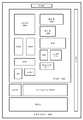
도 5는 본 발명의 예시적 실시예에 따라 구성된 하나 이상의 트랜지스터 구조로 구현된 컴퓨팅 시스템(1000)을 예시한다. 볼 수 있는 바와 같이, 컴퓨팅 시스템(1000)은 마더보드(1002)를 수용한다. 마더보드(1002)는, 이에 제한되지는 않지만, 각각 마더보드(1002)에 물리적 및 전기적으로 연결될 수 있거나 그 안에 통합된, 프로세서(1004) 및 적어도 하나의 통신 칩(1006)을 포함하는 다수의 구성요소를 포함할 수 있다. 이해되는 바와 같이, 마더보드(1002)는, 예를 들어, 메인 보드, 또는 메인 보드상에 탑재된 도터 보드(daughterboard), 또는 시스템(1000)의 유일한 보드 등일 수 있는 임의의 인쇄 회로 기판일 수 있다. 응용에 따라, 컴퓨팅 시스템(1000)은 마더보드(1002)에 물리적 및 전기적으로 연결될 수 있거나 연결되지 않을 수 있는 하나 이상의 다른 구성요소를 포함할 수 있다. 상기 다른 구성요소는, 이에 제한되지는 않지만 휘발성 메모리(예를 들어, DRAM), 비휘발성 메모리(예를 들어, ROM), 그래픽 프로세서, 디지털 신호 처리기, 암호 처리기, 칩셋, 안테나, 디스플레이, 터치스크린 디스플레이, 터치스크린 제어기, 배터리, 오디오 코덱, 비디오 코덱, 전력 증폭기, GPS 장치, 콤파스, 가속도계, 자이로스코프, 스피커, 카메라 및 대용량 저장 장치(예를 들어, 하드 디스크 드라이브, CD, DVD 등)를 포함할 수 있다. 컴퓨팅 시스템(1000)에 포함된 임의의 구성요소는 본 출원에 설명된 하나 이상의 트랜지스터 구조(예를 들어, 더 낮은 콘택 저항/향상된 전도율을 제공하기 위해 n-형 및 p-형 소스/드레인 영역 모두의 위에 작은 밴드 갭의 또는 적절히 도핑된 III-V 재료 층을 갖는)를 포함할 수 있다. 이들 트랜지스터 구조는, 예를 들어 온-보드 프로세서 캐쉬 또는 메모리 어레이를 구현하기 위해 사용될 수 있다. 일부 실시예에서, 복수의 기능들이 하나 이상의 칩에 통합될 수 있다(예를 들어, 통신 칩(1006)은 프로세서(1004)의 일부일 수 있거나 그에 통합될 수 있음을 주목함).FIG. 5 illustrates a computing system 1000 implemented with one or more transistor structures constructed in accordance with an exemplary embodiment of the invention. As can be seen, the computing system 1000 accommodates the motherboard 1002. The motherboard 1002 includes a plurality of motherboards 1002 including a processor 1004 and at least one
통신 칩(1006)은 컴퓨팅 시스템(1000)에 및 컴퓨팅 시스템(1000)으로부터 데이터를 전송하기 위한 무선 통신을 가능하게 한다. 용어 "무선" 및 그의 파생어는 비-고형 매체를 통해 변조 전자기 복사를 사용함으로써 데이터를 통신할 수 있는, 회로, 장치, 시스템, 방법, 기술, 통신 채널 등을 설명하기 위해 사용될 수 있다. 용어는, 비록 일부 실시예에서는 그렇지 않을 수도 있지만, 관련 장치가 임의의 와이어를 포함하지 않음을 시사하지 않는다. 통신 칩(1006)은, 이에 제한되지는 않지만 Wi-Fi(IEEE 802.11 그룹), WiMAX(IEEE 802.16 그룹), IEEE 802.20, LTE(long term evolution), Ev-DO, HSPA+, HSDPA+, HSUPA+, EDGE, GSM, GPRS, CDMA, TDMA, DECT, 블루투스, 그의 파생물 뿐만 아니라 3G, 4G, 5G 및 그 이상으로 지정된 임의의 다른 무선 프로토콜을 포함하는, 임의의 다수의 무선 표준 또는 프로토콜을 구현할 수 있다. 컴퓨팅 시스템(1000)은 복수의 통신 칩(1006)을 포함할 수 있다. 예를 들어, 제1 통신 칩(1006)은 Wi-Fi 및 블루투스와 같은 근거리 무선 통신 전용일 수 있으며, 제2 통신 칩(1006)은 GPS, EDGE, GPRS, CDMA, WiMAX, LTE, Ev-DO 및 기타와 같은 장거리 무선 통신 전용일 수 있다.The
컴퓨팅 시스템(1000)의 프로세서(1004)는 프로세서(1004) 내에 패키징된 집적 회로 다이를 포함한다. 본 발명의 일부 실시예에서, 프로세서의 집적 회로 다이는 본 출원에 설명된 바와 같은 하나 이상의 CMOS 트랜지스터 구조로 구현된 온-보드 메모리 회로를 포함한다. 용어 "프로세서"는, 예를 들어 레지스터 및/또는 메모리로부터 전자 데이터를 처리하여 그 전자 데이터를 레지스터 및/또는 메모리에 저장될 수 있는 다른 전자 데이터로 변형하는 임의의 장치 또는 장치의 일부를 지칭할 수 있다.The processor 1004 of the computing system 1000 includes an integrated circuit die packaged within the processor 1004. In some embodiments of the invention, the integrated circuit die of the processor includes an on-board memory circuit implemented in one or more CMOS transistor structures as described in the present application. The term "processor" refers, for example, to any device or portion of a device that processes electronic data from a register and / or memory and transforms the electronic data into other electronic data that may be stored in a register and / .
통신 칩(1006)은 또한 통신 칩(1006) 내에 패키징된 집적 회로 다이를 포함할 수 있다. 상기 일부 예시적 실시예에 따라, 통신 칩의 집적 회로 다이는 본 출원에 설명된 바와 같은 하나 이상의 트랜지스터 구조로 구현된 하나 이상의 장치(예를 들어, 온-칩 프로세서 또는 메모리)를 포함한다. 본 발명의 관점에서 이해되는 바와 같이, 복수 표준 무선 기능이 프로세서(1004)에 직접 통합(예를 들어, 별도의 통신 칩을 갖지 않고 임의의 칩(1006)의 기능이 프로세서(1004)에 통합)될 수 있음을 주목한다. 프로세서(1004)는 상기 무선 기능을 갖는 칩셋일 수 있음을 추가로 주목한다. 즉, 임의의 수의 프로세서(1004) 및/또는 통신 칩(1006)을 사용할 수 있다. 이와 유사하게, 임의의 하나의 칩 또는 칩셋은 그 안에 통합된 복수의 기능을 가질 수 있다.The
각종 구현에서, 컴퓨팅 시스템(1000)은 랩톱, 넷북, 노트북, 스마트폰, 태블릿, PDA, 울트라 모바일 PC, 휴대폰, 데스크톱 컴퓨터, 서버, 프린터, 스캐너, 모니터, 셋-톱 박스, 엔터테인먼트 제어 유닛, 디지털 카메라, 휴대용 음악 플레이어, 또는 디지털 비디오 레코더일 수 있다. 추가 구현에서, 시스템(1000)은 데이터를 처리하거나 본 출원에 설명된 바와 같은 낮은 콘택 저항 트랜지스터 디바이스(예를 들어, p 및 n형 디바이스 모두를 갖는 CMOS 디바이스)를 사용하는 임의의 다른 전자 디바이스일 수 있다.In various implementations, the computing system 1000 may be a personal computer, such as a laptop, a netbook, a notebook, a smartphone, a tablet, a PDA, an ultra mobile PC, a mobile phone, a desktop computer, a server, a printer, a scanner, A camera, a portable music player, or a digital video recorder. In a further implementation, system 1000 may be any other electronic device that processes data or uses a low contact resistance transistor device (e.g., a CMOS device having both p and n type devices) as described in this application .
다수의 실시예가 명백할 것이며, 본 출원에 설명된 특징은 임의의 수의 구성으로 조합될 수 있다. 본 발명의 한 예시적 실시예는 반도체 집적 회로를 제공한다. 집적 회로는 다수의 채널 영역을 갖는 기판, 및 각 채널 영역 위의 게이트 전극을 포함하며, 여기서 각 게이트 전극과 상응하는 채널 영역 사이에 게이트 유전체 층이 제공된다. 집적 회로는 기판 내의 및 상응하는 채널 영역에 인접하는 p-형 소스/드레인 영역, 및 기판 내의 및 상응하는 채널 영역에 인접하는 n-형 소스/드레인 영역을 추가로 포함한다. 집적 회로는 적어도 p-형 소스/드레인 영역의 일부 및 n-형 소스 드레인 영역의 일부 상에 III-V 반도체 재료 층을 추가로 포함한다. 집적 회로는 III-V 반도체 재료 층 상에 금속 콘택을 추가로 포함한다. 일부 경우에, III-V 반도체 재료 층은 도핑되지 않는다. 일부 예시적 경우에, III-V 반도체 재료 층의 밴드 갭은 0.5 eV 미만이다. 다른 예시적 경우에, III-V 반도체 재료 층은 밴드 갭이 0.2 eV 미만이다. 일부 경우에, III-V 반도체 재료 층이 도핑된다. 상기 일부 경우에, III-V 반도체 재료 층은 p-형 및 n-형 소스/드레인 영역 양쪽에 대한 것과 동일한 도핑 체계를 갖는다. 상기 다른 경우에, III-V 반도체 재료 층은 p-형 소스/드레인 영역을 위한 제1 도핑 체계 및 n-형 소스/드레인 영역을 위한 제2 도핑 체계를 갖는다. III-V 반도체 재료 층은, 예를 들어 하나 이상의 양쪽성 도펀트(C, Si, Ge 및/또는 Sn)로 도핑될 수 있다. 상기 한 경우에, III-V 반도체 재료 층은 1E18 atoms/cm3 치환 농도보다 크게 하나 이상의 양쪽성 도펀트로 도핑된다. 디바이스는 예를 들어 평면 트랜지스터 아키텍처 또는 비-평면 트랜지스터 아키텍처로 구현될 수 있다. 상기 한 경우에, 비-평면 트랜지스터 아키텍처는 FinFET 트랜지스터 및/또는 나노와이어 트랜지스터의 적어도 하나를 포함한다. 일부 경우에, p-형 및 n-형 소스/드레인 영역은 실리콘, 게르마늄, 또는 그의 합금을 포함한다. 본 발명의 다른 실시예는, 이 단락에서 다양하게 정의된 바와 같은 하나 이상의 집적 회로를 갖는 인쇄 회로 기판을 포함하는 전자 디바이스를 제공한다. 상기 한 경우에, 하나 이상의 집적 회로는 통신 칩 및/또는 프로세서의 적어도 하나를 포함한다. 장치는 예를 들어 컴퓨팅 장치일 수 있다.Many embodiments will be apparent, and the features described in this application may be combined in any number of configurations. One exemplary embodiment of the present invention provides a semiconductor integrated circuit. The integrated circuit includes a substrate having a plurality of channel regions, and a gate electrode over each channel region, wherein a gate dielectric layer is provided between each gate electrode and a corresponding channel region. The integrated circuit further includes a p-type source / drain region in the substrate and adjacent to the corresponding channel region, and an n-type source / drain region in the substrate and adjacent to the corresponding channel region. The integrated circuit further includes a layer of III-V semiconductor material on at least a portion of the p-type source / drain region and a portion of the n-type source drain region. The integrated circuit further includes a metal contact on the III-V semiconductor material layer. In some cases, the III-V semiconductor material layer is not doped. In some exemplary cases, the bandgap of the III-V semiconductor material layer is less than 0.5 eV. In another exemplary case, the III-V semiconductor material layer has a band gap of less than 0.2 eV. In some cases, the III-V semiconductor material layer is doped. In this case, the III-V semiconductor material layer has the same doping system as for both p-type and n-type source / drain regions. In the other case, the III-V semiconductor material layer has a first doping scheme for the p-type source / drain region and a second doping scheme for the n-type source / drain region. The III-V semiconductor material layer may be doped, for example, with one or more amphoteric dopants (C, Si, Ge and / or Sn). If the above-described, III-V semiconductor material layer is doped with one or more large amphoteric dopant than 1E18 atoms / cm3 substituted concentration. The device may be implemented with, for example, a planar transistor architecture or a non-planar transistor architecture. In the above case, the non-planar transistor architecture includes at least one of a FinFET transistor and / or a nanowire transistor. In some cases, the p-type and n-type source / drain regions include silicon, germanium, or alloys thereof. Another embodiment of the present invention provides an electronic device comprising a printed circuit board having one or more integrated circuits as variously defined in this paragraph. In the above case, the at least one integrated circuit includes at least one of a communication chip and / or a processor. The device may be, for example, a computing device.
본 발명의 다른 실시예는 다수의 채널 영역을 갖는 실리콘-함유 기판, 및 각 채널 영역 위의 게이트 전극을 포함하는 디바이스를 제공하며, 여기서 각 게이트 전극과 상응하는 채널 영역 사이에 게이트 유전체 층이 제공된다. 디바이스는, 실리콘, 게르마늄 또는 그의 합금을 포함하며 기판 내의 및 상응하는 채널 영역에 인접하는 p-형 소스/드레인 영역, 및 실리콘, 게르마늄 또는 그의 합금을 포함하며 기판 내의 및 상응하는 채널 영역에 인접하는 n-형 소스/드레인 영역을 추가로 포함한다. 디바이스는, 적어도 p-형 소스/드레인 영역의 일부 및 n-형 소스/드레인 영역의 일부 상의 III-V 반도체 재료 층, 및 p-형 및 n-형 소스/드레인 영역 각각에 대한 III-V 반도체 재료 층 상의 금속 콘택을 추가로 포함한다. 한 특정 예시적 실시예에 따라, Si, SiGe 합금 및 Ge 소스/드레인 영역 상에 InSb의 III-V 재료 퇴적은 전도에 대해 매우 낮은 배리어가 산출되도록 시뮬레이션에 의해 예측된다. 본 발명의 관점에서 다른 적절한 III-V 재료 층이 명백할 것이다. 일부 경우에, III-V 반도체 재료 층은 도핑되지 않는다. 일부 경우에, III-V 반도체 재료 층의 밴드 갭은 0.5 eV 미만이다. 일부 경우에, III-V 반도체 재료 층은 도핑된다. 상기 일부 경우에, III-V 반도체 재료 층은 p-형 및 n-형 소스/드레인 영역 양쪽에 대한 것과 동일한 도핑 체계를 갖는다. 상기 다른 경우에, III-V 반도체 재료 층은 p-형 소스/드레인 영역을 위한 제1 도핑 체계 및 n-형 소스/드레인 영역을 위한 제2 도핑 체계를 갖는다. 일부 경우에, III-V 반도체 재료 층은 Ge와 같은 하나 이상의 양쪽성 도펀트로(예를 들어, 1E18 atoms/cm3 치환 농도보다 크게) 도핑된다.Another embodiment of the present invention provides a device comprising a silicon-containing substrate having a plurality of channel regions and a gate electrode over each channel region, wherein a gate dielectric layer is provided between each gate electrode and a corresponding channel region do. The device comprises silicon, germanium, or an alloy thereof and includes a p-type source / drain region in the substrate and adjacent to the corresponding channel region, and a source / drain region adjacent to the corresponding channel region type source / drain regions. The device comprises a III-V semiconductor material layer on at least a portion of a p-type source / drain region and a portion of an n-type source / drain region, and a III-V semiconductor material for each of p- Further comprising a metal contact on the material layer. According to one particular illustrative embodiment, III-V material deposition of InSb on Si, SiGe alloy and Ge source / drain regions is predicted by simulation to yield a very low barrier to conduction. Other suitable III-V material layers will be apparent in light of the present invention. In some cases, the III-V semiconductor material layer is not doped. In some cases, the bandgap of the III-V semiconductor material layer is less than 0.5 eV. In some cases, the III-V semiconductor material layer is doped. In this case, the III-V semiconductor material layer has the same doping system as for both p-type and n-type source / drain regions. In the other case, the III-V semiconductor material layer has a first doping scheme for the p-type source / drain region and a second doping scheme for the n-type source / drain region. In some cases, III-V semiconductor material layer with one or more amphoteric dopant such as Ge is doped (for example, greater than 1E18 atoms / cm3 substituted concentration).
본 발명의 다른 실시예는 반도체 디바이스의 형성 방법을 제공한다. 방법은 다수의 채널 영역을 갖는 기판을 제공하는 단계, 및 각 채널 영역 위에 게이트 전극을 제공하며, 여기서 각 게이트 전극과 상응하는 채널 영역 사이에 게이트 유전체 층이 제공되는 단계를 포함한다. 방법은 기판 내의 및 상응하는 채널 영역에 인접하는 p-형 소스/드레인 영역을 제공하는 단계, 및 기판 내의 및 상응하는 채널 영역에 인접하는 n-형 소스/드레인 영역을 제공하는 단계를 추가로 포함한다. 방법은 적어도 p-형 소스/드레인 영역의 일부 및 n-형 소스/드레인 영역의 일부 상에 III-V 반도체 재료 층을 제공하는 단계를 추가로 포함한다. 방법은 III-V 반도체 재료 층 상에 금속 콘택을 제공하는 단계를 추가로 포함한다.Another embodiment of the present invention provides a method of forming a semiconductor device. The method includes providing a substrate having a plurality of channel regions, and providing a gate electrode over each channel region, wherein a gate dielectric layer is provided between each gate electrode and a corresponding channel region. The method further includes providing a p-type source / drain region in the substrate and adjacent to the corresponding channel region, and providing an n-type source / drain region in the substrate and adjacent to the corresponding channel region do. The method further includes providing a layer of a III-V semiconductor material on at least a portion of the p-type source / drain region and a portion of the n-type source / drain region. The method further comprises providing a metal contact on the III-V semiconductor material layer.
본 발명의 실시예의 전술한 설명은 예시 및 설명의 목적으로 제시되었다. 이는 완전하거나, 본 발명을 개시된 정확한 형태로 한정하는 것을 의도하지 않는다. 본 발명의 관점에서 다수의 변형 및 변경이 가능하다. 본 발명의 범위는 본 상세한 설명에 의해서가 아니라 본 출원에 첨부된 청구항에 의해 한정됨을 의도한다.The foregoing description of the embodiments of the invention has been presented for purposes of illustration and description. It is not intended to be exhaustive or to limit the invention to the precise form disclosed. Many modifications and variations are possible in light of the present invention. It is intended that the scope of the invention be limited not by this detailed description, but rather by the claims appended hereto.
Claims (25)
Translated fromKorean실리콘 또는 게르마늄 중 하나 또는 모두를 포함하는 p-형 소스/드레인 영역들;
실리콘 또는 게르마늄 중 하나 또는 모두를 포함하는 n-형 소스/드레인 영역들;
상기 p-형 소스/드레인 영역들 및 상기 n-형 소스/드레인 영역들의 각각 위에 콘택 트랜치를 갖는 절연체 층;
상기 p-형 소스/드레인 영역들의 적어도 일부 및 상기 n-형 소스/드레인 영역들의 적어도 일부 상의 III-V 반도체 재료 층 - 상기 III-V 반도체 재료 층은 상기 III-V 반도체 재료 층의 적어도 일부에 도펀트를 포함하고, 상기 III-V 반도체 재료 층은 완전히 상기 콘택 트랜치들 내에 있음 -; 및
상기 III-V 반도체 재료 층 상의 적어도 하나의 콘택 구조
를 포함하는 집적 회로.As an integrated circuit,
P-type source / drain regions comprising one or both of silicon or germanium;
N-type source / drain regions comprising one or both of silicon or germanium;
An insulator layer having a contact trench on each of the p-type source / drain regions and the n-type source / drain regions;
At least a portion of the p-type source / drain regions and a III-V semiconductor material layer on at least a portion of the n-type source / drain regions, the III-V semiconductor material layer being formed on at least a portion of the III- Dopant, the III-V semiconductor material layer being entirely in the contact trenches; And
At least one contact structure on the III-V semiconductor material layer
≪ / RTI >
상기 소스/드레인 영역들의 일부 위의 III-V 반도체 재료 층은 도핑되지 않은 집적 회로.The method according to claim 1,
Wherein the III-V semiconductor material layer over a portion of the source / drain regions is undoped.
상기 소스/드레인 영역들의 모두 위의 III-V 반도체 재료 층은 도핑된 집적 회로.The method according to claim 1,
The III-V semiconductor material layer above all of the source / drain regions is doped.
상기 III-V 반도체 재료 층은 상기 p-형 및 n-형 소스/드레인 영역들의 모두에 대하여 동일한 도핑 체계를 갖는 집적 회로.The method according to claim 1,
Wherein the III-V semiconductor material layer has the same doping system for both the p-type and n-type source / drain regions.
상기 III-V 반도체 재료 층은 상기 p-형 소스/드레인 영역들에 대하여 제1 도핑 체계를 갖고 상기 n-형 소스/드레인 영역들에 대하여 제2 도핑 체계를 갖고, 상기 제1 도핑 체계는 상기 제2 도핑 체계와는 상이한 집적 회로.The method according to claim 1,
Wherein the III-V semiconductor material layer has a first doping system for the p-type source / drain regions and a second doping system for the n-type source / drain regions, An integrated circuit different from the second doping system.
상기 III-V 반도체 재료 층에 포함된 도펀트는 하나 이상의 양쪽성 도펀트인 집적 회로.The method according to claim 1,
Wherein the dopant included in the III-V semiconductor material layer is at least one amphoteric dopant.
상기 p-형 및 n-형 소스/드레인 영역들의 각각은 실리콘을 포함하는 집적 회로.7. The method according to any one of claims 1 to 6,
And wherein each of the p-type and n-type source / drain regions comprises silicon.
상기 p-형 및 n-형 소스/드레인 영역들 중 하나 이상의 반도체 재료는 기판과 조성적으로 다르고 상기 기판의 일부가 아닌 집적 회로.7. The method according to any one of claims 1 to 6,
Wherein at least one of the p-type and n-type source / drain regions of the semiconductor material is compositionally different from the substrate and is not part of the substrate.
상기 p-형 소스/드레인 영역들 사이의 제1 바디와 상기 n-형 소스/드레인 영역들 사이의 제2 바디를 더 포함하고, 상기 제1 및 제2 바디들의 각각은 실리콘 또는 게르마늄 중 하나 또는 모두를 포함하는 집적 회로.7. The method according to any one of claims 1 to 6,
And a second body between the p-type source / drain regions and a second body between the n-type source / drain regions, wherein each of the first and second bodies comprises one of silicon or germanium, An integrated circuit including all of the above.
상기 제1 또는 제2 바디들 중 하나 또는 모두는 핀(fin) 형태인 집적 회로.10. The method of claim 9,
Wherein one or both of the first or second bodies are in the form of a fin.
게이트 구조를 더 포함하고, 상기 게이트 구조는 상기 핀 형태의 바디들의 3면에 인접한 집적 회로.11. The method of claim 10,
Further comprising a gate structure, said gate structure being adjacent to three sides of said pinned bodies.
상기 제1 또는 제2 바디들 중 하나 또는 모두는 나노와이어 형태인 집적 회로.10. The method of claim 9,
Wherein one or both of the first or second bodies are nanowire-shaped.
게이트 구조를 더 포함하고, 상기 게이트 구조는 상기 나노와이어 형태의 바디들을 둘러싸는 집적 회로.13. The method of claim 12,
Further comprising a gate structure, said gate structure surrounding said nanowire-shaped bodies.
상기 III-V 반도체 재료 층은 0.5 eV 미만의 밴드갭을 갖는 집적 회로.7. The method according to any one of claims 1 to 6,
Wherein the III-V semiconductor material layer has a bandgap of less than 0.5 eV.
기판;
제1 및 제2 핀들을 포함하는 복수의 핀들;
실리콘, 게르마늄, 또는 실리콘 게르마늄을 포함하는 반도체 재료를 포함하는 p-형 소스/드레인 영역들;
실리콘, 게르마늄, 또는 실리콘 게르마늄을 포함하는 반도체 재료를 포함하는 n-형 소스/드레인 영역들;
상기 기판 위의 절연체 층 - 상기 절연체 층은 상기 p-형 소스/드레인 영역들 및 상기 n-형 소스/드레인 영역들의 각각 위에 콘택 트랜치를 가짐 -;
상기 p-형 소스/드레인 영역들의 적어도 일부 및 상기 n-형 소스/드레인 영역들의 적어도 일부 상의 III-V 반도체 재료 층 - 상기 III-V 반도체 재료 층은 0.5 eV 미만의 밴드갭 또는 포함된 도펀트 중 하나 또는 모두를 포함하고, 상기 III-V 반도체 재료 층은 완전히 상기 콘택 트랜치들 내에 있음 -; 및
상기 III-V 반도체 재료 층 상의 적어도 하나의 콘택 구조
를 포함하고,
상기 제1 또는 제2 핀들 중 하나 또는 모두는 상기 기판과 조성적으로 다르고 상기 기판의 일부가 아닌 반도체 재료를 포함하는 집적 회로.As an integrated circuit,
Board;
A plurality of pins including first and second pins;
P-type source / drain regions comprising a semiconductor material comprising silicon, germanium, or silicon germanium;
N-type source / drain regions comprising a semiconductor material comprising silicon, germanium, or silicon germanium;
An insulator layer over the substrate, the insulator layer having a contact trench on each of the p-type source / drain regions and the n-type source / drain regions;
At least a portion of the p-type source / drain regions and a III-V semiconductor material layer on at least a portion of the n-type source / drain regions, the III-V semiconductor material layer having a bandgap of less than 0.5 eV, One or both, said III-V semiconductor material layer being completely within said contact trenches; And
At least one contact structure on the III-V semiconductor material layer
Lt; / RTI >
Wherein one or both of the first or second fins are semiconductor materials that are compositionally different from the substrate and are not part of the substrate.
제1 소스 영역 및 제1 드레인 영역 - 상기 제1 소스 및 드레인 영역들의 각각은 실리콘 또는 게르마늄 중 하나 또는 모두를 포함하고, p-형 도펀트도 포함함 -;
제2 소스 영역 및 제2 드레인 영역 - 상기 제2 소스 및 드레인 영역들의 각각은 실리콘 또는 게르마늄 중 하나 또는 모두를 포함하고, n-형 도펀트도 포함함 -;
상기 제1 소스 및 드레인 영역들 및 상기 제2 소스 및 드레인 영역들의 각각 위에 콘택 트랜치를 갖는 절연체 층;
상기 제1 소스 및 드레인 영역들의 각각의 위의 제1 콘택 구조;
상기 제2 소스 및 드레인 영역들의 각각의 위의 제2 콘택 구조;
상기 제1 소스 영역 및 대응하는 제1 콘택 구조 사이의 층 - 상기 층은 상기 제1 드레인 영역 및 대응하는 제1 콘택 구조 사이에도 있고, 상기 층은 상기 제2 소스 영역 및 대응하는 제2 콘택 구조 사이에도 있고, 상기 층은 상기 제2 드레인 영역 및 대응하는 제2 콘택 구조 사이에도 있고, 상기 층은 알루미늄, 갈륨, 또는 인듐 중 하나 이상을 포함하고, 상기 층은 인, 비소, 또는 안티몬 중 하나 이상도 포함하고, 상기 층은 상기 층의 적어도 일부에 n-형 또는 p-형 도펀트를 더 포함하고, 상기 층은 완전히 상기 콘택 트랜치들 내에 있음 -
을 포함하는 집적 회로.As an integrated circuit,
A first source region and a first drain region, each of said first source and drain regions comprising one or both of silicon or germanium and also comprising a p-type dopant;
A second source region and a second drain region, each of said second source and drain regions comprising one or both of silicon or germanium and also comprising an n-type dopant;
An insulator layer having a contact trench on each of the first source and drain regions and the second source and drain regions;
A first contact structure over each of the first source and drain regions;
A second contact structure over each of the second source and drain regions;
A layer between the first source region and a corresponding first contact structure, the layer being also between the first drain region and a corresponding first contact structure, the layer comprising a second source region and a corresponding second contact structure, Wherein said layer is also between said second drain region and a corresponding second contact structure, said layer comprising at least one of aluminum, gallium, or indium, said layer comprising one of phosphorous, arsenic, or antimony Wherein the layer further comprises an n-type or p-type dopant in at least a portion of the layer, the layer being completely within the contact trenches,
≪ / RTI >
상기 층은 안티몬 또는 비소 중 하나 또는 모두와 인듐을 포함하는 집적 회로.17. The method of claim 16,
Wherein the layer comprises one or both of antimony or arsenic and indium.
상기 제1 소스 및 드레인 영역들 사이의 제1 바디;
상기 제1 바디에 근접한 제1 금속 게이트 구조;
상기 제2 소스 및 드레인 영역들 사이의 제2 바디; 및
상기 제2 바디에 근접한 제2 금속 게이트 구조
를 더 포함하는 집적 회로.18. The method according to claim 16 or 17,
A first body between the first source and drain regions;
A first metal gate structure proximate the first body;
A second body between the second source and drain regions; And
A second metal gate structure proximate the second body
≪ / RTI >
상기 제1 또는 제2 바디들 중 하나 또는 모두는 핀 형태로서, 대응하는 금속 게이트 구조가 상기 핀 형태의 바디들의 3면에 근접하도록 되어 있는 집적 회로.19. The method of claim 18,
Wherein one or both of said first or second bodies are in the form of a pin such that a corresponding metal gate structure is proximate to three sides of said bodies in the form of a pin.
상기 제1 또는 제2 바디들 중 하나 또는 모두는 나노와이어 형태로서, 대응하는 금속 게이트 구조가 상기 나노와이어 형태의 바디들을 둘러싸도록 되어 있는 집적 회로.19. The method of claim 18,
Wherein one or both of said first or second bodies are in the form of nanowires such that a corresponding metal gate structure surrounds said nanowire shaped bodies.
제1 소스 영역 및 제1 드레인 영역 - 상기 제1 소스 및 드레인 영역들의 각각은 실리콘 또는 게르마늄 중 하나 또는 모두를 포함하고, p-형 도펀트도 포함함 -;
제2 소스 영역 및 제2 드레인 영역 - 상기 제2 소스 및 드레인 영역들의 각각은 실리콘 또는 게르마늄 중 하나 또는 모두를 포함하고, n-형 도펀트도 포함함 -;
상기 제1 소스 및 드레인 영역들 및 상기 제2 소스 및 드레인 영역들의 각각 위에 콘택 트랜치를 갖는 절연체 층;
상기 제1 소스 및 드레인 영역들의 각각의 위의 제1 콘택 구조;
상기 제2 소스 및 드레인 영역들의 각각의 위의 제2 콘택 구조; 및
상기 제1 소스 영역 및 대응하는 제1 콘택 구조 사이의 층 - 상기 층은 상기 제1 드레인 영역 및 대응하는 제1 콘택 구조 사이에도 있고, 상기 층은 상기 제2 소스 영역 및 대응하는 제2 콘택 구조 사이에도 있고, 상기 층은 상기 제2 드레인 영역 및 대응하는 제2 콘택 구조 사이에도 있고, 상기 층은 알루미늄, 갈륨, 또는 인듐 중 하나 이상을 포함하고, 상기 층은 인, 비소, 또는 안티몬 중 하나 이상도 포함하고, 상기 층은 0.5 eV 미만의 밴드갭을 갖고, 상기 층은 완전히 상기 콘택 트랜치들 내에 있음 -
을 포함하는 집적 회로.As an integrated circuit,
A first source region and a first drain region, each of said first source and drain regions comprising one or both of silicon or germanium and also comprising a p-type dopant;
A second source region and a second drain region, each of said second source and drain regions comprising one or both of silicon or germanium and also comprising an n-type dopant;
An insulator layer having a contact trench on each of the first source and drain regions and the second source and drain regions;
A first contact structure over each of the first source and drain regions;
A second contact structure over each of the second source and drain regions; And
A layer between the first source region and a corresponding first contact structure, the layer being also between the first drain region and a corresponding first contact structure, the layer comprising a second source region and a corresponding second contact structure, Wherein said layer is also between said second drain region and a corresponding second contact structure, said layer comprising at least one of aluminum, gallium, or indium, said layer comprising one of phosphorous, arsenic, or antimony Wherein the layer has a bandgap less than 0.5 eV and the layer is completely within the contact trenches,
≪ / RTI >
상기 층은 상기 층의 적어도 일부에 n-형 또는 p-형 도펀트를 더 포함하는 집적 회로.22. The method of claim 21,
Said layer further comprising an n-type or p-type dopant in at least a portion of said layer.
상기 제1 소스 및 드레인 영역들 사이의 제1 바디;
상기 제1 바디에 근접한 제1 금속 게이트 구조;
상기 제2 소스 및 드레인 영역들 사이의 제2 바디; 및
상기 제2 바디에 근접한 제2 금속 게이트 구조
를 더 포함하는 집적 회로.23. The method of claim 21 or 22,
A first body between the first source and drain regions;
A first metal gate structure proximate the first body;
A second body between the second source and drain regions; And
A second metal gate structure proximate the second body
≪ / RTI >
상기 제1 또는 제2 바디들 중 하나 또는 모두는 핀 형태로서, 대응하는 금속 게이트 구조가 상기 핀 형태의 바디들의 3면에 근접하도록 되어 있는 집적 회로.24. The method of claim 23,
Wherein one or both of said first or second bodies are in the form of a pin such that a corresponding metal gate structure is proximate to three sides of said bodies in the form of a pin.
상기 제1 또는 제2 바디들 중 하나 또는 모두는 나노와이어 형태로서, 대응하는 금속 게이트 구조가 상기 나노와이어 형태의 바디들을 둘러싸도록 되어 있는 집적 회로.
24. The method of claim 23,
Wherein one or both of said first or second bodies are in the form of nanowires such that a corresponding metal gate structure surrounds said nanowire shaped bodies.
Applications Claiming Priority (1)
| Application Number | Priority Date | Filing Date | Title |
|---|---|---|---|
| PCT/US2011/066132WO2013095375A1 (en) | 2011-12-20 | 2011-12-20 | Iii-v layers for n-type and p-type mos source-drain contacts |
Related Parent Applications (1)
| Application Number | Title | Priority Date | Filing Date |
|---|---|---|---|
| KR1020167009740ADivisionKR101790605B1 (en) | 2011-12-20 | 2011-12-20 | Semiconductor device having iii-v semiconductor material layer |
Publications (2)
| Publication Number | Publication Date |
|---|---|
| KR20170120208A KR20170120208A (en) | 2017-10-30 |
| KR101891458B1true KR101891458B1 (en) | 2018-08-24 |
Family
ID=48669033
Family Applications (3)
| Application Number | Title | Priority Date | Filing Date |
|---|---|---|---|
| KR1020177030300AActiveKR101891458B1 (en) | 2011-12-20 | 2011-12-20 | Semiconductor device having iii-v semiconductor material layer |
| KR1020167009740AActiveKR101790605B1 (en) | 2011-12-20 | 2011-12-20 | Semiconductor device having iii-v semiconductor material layer |
| KR1020147017474ACeasedKR20140097464A (en) | 2011-12-20 | 2011-12-20 | Iii-v layers for n-type and p-type mos source-drain contacts |
Family Applications After (2)
| Application Number | Title | Priority Date | Filing Date |
|---|---|---|---|
| KR1020167009740AActiveKR101790605B1 (en) | 2011-12-20 | 2011-12-20 | Semiconductor device having iii-v semiconductor material layer |
| KR1020147017474ACeasedKR20140097464A (en) | 2011-12-20 | 2011-12-20 | Iii-v layers for n-type and p-type mos source-drain contacts |
Country Status (5)
| Country | Link |
|---|---|
| US (3) | US9153583B2 (en) |
| KR (3) | KR101891458B1 (en) |
| DE (1) | DE112011105972B4 (en) |
| TW (1) | TWI567987B (en) |
| WO (1) | WO2013095375A1 (en) |
Families Citing this family (430)
| Publication number | Priority date | Publication date | Assignee | Title |
|---|---|---|---|---|
| US10378106B2 (en) | 2008-11-14 | 2019-08-13 | Asm Ip Holding B.V. | Method of forming insulation film by modified PEALD |
| US9394608B2 (en) | 2009-04-06 | 2016-07-19 | Asm America, Inc. | Semiconductor processing reactor and components thereof |
| US8802201B2 (en) | 2009-08-14 | 2014-08-12 | Asm America, Inc. | Systems and methods for thin-film deposition of metal oxides using excited nitrogen-oxygen species |
| US9312155B2 (en) | 2011-06-06 | 2016-04-12 | Asm Japan K.K. | High-throughput semiconductor-processing apparatus equipped with multiple dual-chamber modules |
| US10364496B2 (en) | 2011-06-27 | 2019-07-30 | Asm Ip Holding B.V. | Dual section module having shared and unshared mass flow controllers |
| US10854498B2 (en) | 2011-07-15 | 2020-12-01 | Asm Ip Holding B.V. | Wafer-supporting device and method for producing same |
| US20130023129A1 (en) | 2011-07-20 | 2013-01-24 | Asm America, Inc. | Pressure transmitter for a semiconductor processing environment |
| US9017481B1 (en) | 2011-10-28 | 2015-04-28 | Asm America, Inc. | Process feed management for semiconductor substrate processing |
| US8896066B2 (en) | 2011-12-20 | 2014-11-25 | Intel Corporation | Tin doped III-V material contacts |
| KR101891458B1 (en)* | 2011-12-20 | 2018-08-24 | 인텔 코포레이션 | Semiconductor device having iii-v semiconductor material layer |
| US9653559B2 (en)* | 2011-12-27 | 2017-05-16 | Intel Corporation | Methods to enhance doping concentration in near-surface layers of semiconductors and methods of making same |
| US9142649B2 (en)* | 2012-04-23 | 2015-09-22 | United Microelectronics Corp. | Semiconductor structure with metal gate and method of fabricating the same |
| US9142400B1 (en) | 2012-07-17 | 2015-09-22 | Stc.Unm | Method of making a heteroepitaxial layer on a seed area |
| US9558931B2 (en) | 2012-07-27 | 2017-01-31 | Asm Ip Holding B.V. | System and method for gas-phase sulfur passivation of a semiconductor surface |
| US9659799B2 (en) | 2012-08-28 | 2017-05-23 | Asm Ip Holding B.V. | Systems and methods for dynamic semiconductor process scheduling |
| US9021985B2 (en) | 2012-09-12 | 2015-05-05 | Asm Ip Holdings B.V. | Process gas management for an inductively-coupled plasma deposition reactor |
| US10714315B2 (en) | 2012-10-12 | 2020-07-14 | Asm Ip Holdings B.V. | Semiconductor reaction chamber showerhead |
| US20160376700A1 (en) | 2013-02-01 | 2016-12-29 | Asm Ip Holding B.V. | System for treatment of deposition reactor |
| US9484191B2 (en) | 2013-03-08 | 2016-11-01 | Asm Ip Holding B.V. | Pulsed remote plasma method and system |
| US9589770B2 (en) | 2013-03-08 | 2017-03-07 | Asm Ip Holding B.V. | Method and systems for in-situ formation of intermediate reactive species |
| US10438856B2 (en) | 2013-04-03 | 2019-10-08 | Stmicroelectronics, Inc. | Methods and devices for enhancing mobility of charge carriers |
| US8993054B2 (en) | 2013-07-12 | 2015-03-31 | Asm Ip Holding B.V. | Method and system to reduce outgassing in a reaction chamber |
| US9105707B2 (en)* | 2013-07-24 | 2015-08-11 | International Business Machines Corporation | ZRAM heterochannel memory |
| US9685509B2 (en) | 2013-07-30 | 2017-06-20 | Samsung Electronics Co., Ltd. | Finfet devices including high mobility channel materials with materials of graded composition in recessed source/drain regions |
| US10147793B2 (en) | 2013-07-30 | 2018-12-04 | Samsung Electronics Co., Ltd. | FinFET devices including recessed source/drain regions having optimized depths |
| US9240412B2 (en) | 2013-09-27 | 2016-01-19 | Asm Ip Holding B.V. | Semiconductor structure and device and methods of forming same using selective epitaxial process |
| US9605343B2 (en) | 2013-11-13 | 2017-03-28 | Asm Ip Holding B.V. | Method for forming conformal carbon films, structures conformal carbon film, and system of forming same |
| US9281401B2 (en) | 2013-12-20 | 2016-03-08 | Intel Corporation | Techniques and configurations to reduce transistor gate short defects |
| US9530776B2 (en)* | 2014-01-17 | 2016-12-27 | Taiwan Semiconductor Manufacturing Company, Ltd. | FinFET semiconductor device with germanium diffusion over silicon fins |
| US9236397B2 (en)* | 2014-02-04 | 2016-01-12 | Globalfoundries Inc. | FinFET device containing a composite spacer structure |
| KR102220590B1 (en) | 2014-02-21 | 2021-03-03 | 삼성전자주식회사 | Integrated circuit devices including contacts and method of forming the same |
| US10683571B2 (en) | 2014-02-25 | 2020-06-16 | Asm Ip Holding B.V. | Gas supply manifold and method of supplying gases to chamber using same |
| US10167557B2 (en) | 2014-03-18 | 2019-01-01 | Asm Ip Holding B.V. | Gas distribution system, reactor including the system, and methods of using the same |
| US11015245B2 (en) | 2014-03-19 | 2021-05-25 | Asm Ip Holding B.V. | Gas-phase reactor and system having exhaust plenum and components thereof |
| EP3123516B1 (en)* | 2014-03-26 | 2020-03-04 | Intel Corporation | Iii-n transistors with enhanced breakdown voltage |
| US9947772B2 (en)* | 2014-03-31 | 2018-04-17 | Stmicroelectronics, Inc. | SOI FinFET transistor with strained channel |
| US9299781B2 (en)* | 2014-04-01 | 2016-03-29 | Globalfoundries Inc. | Semiconductor devices with contact structures and a gate structure positioned in trenches formed in a layer of material |
| US9171934B2 (en) | 2014-04-01 | 2015-10-27 | Globalfoundries Inc. | Methods of forming semiconductor devices using a layer of material having a plurality of trenches formed therein |
| US9472628B2 (en) | 2014-07-14 | 2016-10-18 | International Business Machines Corporation | Heterogeneous source drain region and extension region |
| US10858737B2 (en) | 2014-07-28 | 2020-12-08 | Asm Ip Holding B.V. | Showerhead assembly and components thereof |
| US9890456B2 (en) | 2014-08-21 | 2018-02-13 | Asm Ip Holding B.V. | Method and system for in situ formation of gas-phase compounds |
| TWI575748B (en)* | 2014-09-01 | 2017-03-21 | 聯華電子股份有限公司 | P-type field effect transistor and complementary metal oxide semiconductor transistor including the P-type field effect transistor |
| WO2016043748A1 (en) | 2014-09-18 | 2016-03-24 | Intel Corporation | Wurtzite heteroepitaxial structures with inclined sidewall facets for defect propagation control in silicon cmos-compatible semiconductor devices |
| KR102311937B1 (en)* | 2014-09-23 | 2021-10-14 | 삼성전자주식회사 | Semiconductor device having contact plug and method of forming the same |
| US10229991B2 (en) | 2014-09-25 | 2019-03-12 | Intel Corporation | III-N epitaxial device structures on free standing silicon mesas |
| US9657845B2 (en) | 2014-10-07 | 2017-05-23 | Asm Ip Holding B.V. | Variable conductance gas distribution apparatus and method |
| US10941490B2 (en) | 2014-10-07 | 2021-03-09 | Asm Ip Holding B.V. | Multiple temperature range susceptor, assembly, reactor and system including the susceptor, and methods of using the same |
| US10573647B2 (en) | 2014-11-18 | 2020-02-25 | Intel Corporation | CMOS circuits using n-channel and p-channel gallium nitride transistors |
| KR102300403B1 (en) | 2014-11-19 | 2021-09-09 | 에이에스엠 아이피 홀딩 비.브이. | Method of depositing thin film |
| US10056456B2 (en) | 2014-12-18 | 2018-08-21 | Intel Corporation | N-channel gallium nitride transistors |
| KR102263121B1 (en) | 2014-12-22 | 2021-06-09 | 에이에스엠 아이피 홀딩 비.브이. | Semiconductor device and manufacuring method thereof |
| US10497814B2 (en) | 2014-12-23 | 2019-12-03 | Intel Corporation | III-V semiconductor alloys for use in the subfin of non-planar semiconductor devices and methods of forming the same |
| EP3238230A4 (en)* | 2014-12-23 | 2018-08-22 | INTEL Corporation | Diffusion tolerant iii-v semiconductor heterostructures and devices including the same |
| US9502567B2 (en)* | 2015-02-13 | 2016-11-22 | Taiwan Semiconductor Manufacturing Co., Ltd. | Semiconductor fin structure with extending gate structure |
| US9929242B2 (en) | 2015-01-12 | 2018-03-27 | Taiwan Semiconductor Manufacturing Co., Ltd. | Semiconductor device and manufacturing method thereof |
| US9418846B1 (en)* | 2015-02-27 | 2016-08-16 | International Business Machines Corporation | Selective dopant junction for a group III-V semiconductor device |
| US10529542B2 (en) | 2015-03-11 | 2020-01-07 | Asm Ip Holdings B.V. | Cross-flow reactor and method |
| US10276355B2 (en) | 2015-03-12 | 2019-04-30 | Asm Ip Holding B.V. | Multi-zone reactor, system including the reactor, and method of using the same |
| WO2016186654A1 (en) | 2015-05-19 | 2016-11-24 | Intel Corporation | Semiconductor devices with raised doped crystalline structures |
| US9543216B2 (en)* | 2015-06-05 | 2017-01-10 | Globalfoundries Inc. | Integration of hybrid germanium and group III-V contact epilayer in CMOS |
| US10458018B2 (en) | 2015-06-26 | 2019-10-29 | Asm Ip Holding B.V. | Structures including metal carbide material, devices including the structures, and methods of forming same |
| US10388777B2 (en) | 2015-06-26 | 2019-08-20 | Intel Corporation | Heteroepitaxial structures with high temperature stable substrate interface material |
| CN107667430B (en) | 2015-06-26 | 2022-07-22 | 英特尔公司 | High mobility semiconductor source/drain spacers |
| US10546858B2 (en) | 2015-06-27 | 2020-01-28 | Intel Corporation | Low damage self-aligned amphoteric FINFET tip doping |
| KR102352659B1 (en)* | 2015-06-27 | 2022-01-18 | 인텔 코포레이션 | Low Damage Self-Aligned Amphoteric FINFET Tip Doping |
| US9818872B2 (en) | 2015-06-30 | 2017-11-14 | Taiwan Semiconductor Manufacturing Company, Ltd. | Multi-gate device and method of fabrication thereof |
| US10600673B2 (en) | 2015-07-07 | 2020-03-24 | Asm Ip Holding B.V. | Magnetic susceptor to baseplate seal |
| US10043661B2 (en) | 2015-07-13 | 2018-08-07 | Asm Ip Holding B.V. | Method for protecting layer by forming hydrocarbon-based extremely thin film |
| US10083836B2 (en) | 2015-07-24 | 2018-09-25 | Asm Ip Holding B.V. | Formation of boron-doped titanium metal films with high work function |
| US10087525B2 (en) | 2015-08-04 | 2018-10-02 | Asm Ip Holding B.V. | Variable gap hard stop design |
| US9647114B2 (en)* | 2015-08-14 | 2017-05-09 | Asm Ip Holding B.V. | Methods of forming highly p-type doped germanium tin films and structures and devices including the films |
| US9960072B2 (en) | 2015-09-29 | 2018-05-01 | Asm Ip Holding B.V. | Variable adjustment for precise matching of multiple chamber cavity housings |
| US10211308B2 (en) | 2015-10-21 | 2019-02-19 | Asm Ip Holding B.V. | NbMC layers |
| US10322384B2 (en) | 2015-11-09 | 2019-06-18 | Asm Ip Holding B.V. | Counter flow mixer for process chamber |
| US9960273B2 (en)* | 2015-11-16 | 2018-05-01 | Taiwan Semiconductor Manufacturing Company, Ltd. | Integrated circuit structure with substrate isolation and un-doped channel |
| WO2017111869A1 (en) | 2015-12-24 | 2017-06-29 | Intel Corporation | Transition metal dichalcogenides (tmdcs) over iii-nitride heteroepitaxial layers |
| US9627221B1 (en) | 2015-12-28 | 2017-04-18 | Asm Ip Holding B.V. | Continuous process incorporating atomic layer etching |
| US11139308B2 (en) | 2015-12-29 | 2021-10-05 | Asm Ip Holding B.V. | Atomic layer deposition of III-V compounds to form V-NAND devices |
| KR102481427B1 (en)* | 2016-01-13 | 2022-12-27 | 삼성전자주식회사 | Semiconductor device and method for manufacturing the same |
| US10529554B2 (en) | 2016-02-19 | 2020-01-07 | Asm Ip Holding B.V. | Method for forming silicon nitride film selectively on sidewalls or flat surfaces of trenches |
| US10468251B2 (en) | 2016-02-19 | 2019-11-05 | Asm Ip Holding B.V. | Method for forming spacers using silicon nitride film for spacer-defined multiple patterning |
| US10501866B2 (en) | 2016-03-09 | 2019-12-10 | Asm Ip Holding B.V. | Gas distribution apparatus for improved film uniformity in an epitaxial system |
| US10343920B2 (en) | 2016-03-18 | 2019-07-09 | Asm Ip Holding B.V. | Aligned carbon nanotubes |
| US9892913B2 (en) | 2016-03-24 | 2018-02-13 | Asm Ip Holding B.V. | Radial and thickness control via biased multi-port injection settings |
| US10865475B2 (en) | 2016-04-21 | 2020-12-15 | Asm Ip Holding B.V. | Deposition of metal borides and silicides |
| US10087522B2 (en) | 2016-04-21 | 2018-10-02 | Asm Ip Holding B.V. | Deposition of metal borides |
| US10190213B2 (en) | 2016-04-21 | 2019-01-29 | Asm Ip Holding B.V. | Deposition of metal borides |
| US10032628B2 (en) | 2016-05-02 | 2018-07-24 | Asm Ip Holding B.V. | Source/drain performance through conformal solid state doping |
| US10367080B2 (en) | 2016-05-02 | 2019-07-30 | Asm Ip Holding B.V. | Method of forming a germanium oxynitride film |
| KR102592471B1 (en) | 2016-05-17 | 2023-10-20 | 에이에스엠 아이피 홀딩 비.브이. | Method of forming metal interconnection and method of fabricating semiconductor device using the same |
| US11453943B2 (en) | 2016-05-25 | 2022-09-27 | Asm Ip Holding B.V. | Method for forming carbon-containing silicon/metal oxide or nitride film by ALD using silicon precursor and hydrocarbon precursor |
| US9905663B2 (en) | 2016-06-24 | 2018-02-27 | International Business Machines Corporation | Fabrication of a vertical fin field effect transistor with a reduced contact resistance |
| US10388509B2 (en) | 2016-06-28 | 2019-08-20 | Asm Ip Holding B.V. | Formation of epitaxial layers via dislocation filtering |
| US9824921B1 (en)* | 2016-07-06 | 2017-11-21 | Globalfoundries Inc. | Method and apparatus for placing a gate contact inside a semiconductor active region having high-k dielectric gate caps |
| US10612137B2 (en) | 2016-07-08 | 2020-04-07 | Asm Ip Holdings B.V. | Organic reactants for atomic layer deposition |
| US9859151B1 (en) | 2016-07-08 | 2018-01-02 | Asm Ip Holding B.V. | Selective film deposition method to form air gaps |
| US9793135B1 (en) | 2016-07-14 | 2017-10-17 | ASM IP Holding B.V | Method of cyclic dry etching using etchant film |
| US10714385B2 (en) | 2016-07-19 | 2020-07-14 | Asm Ip Holding B.V. | Selective deposition of tungsten |
| KR102354490B1 (en) | 2016-07-27 | 2022-01-21 | 에이에스엠 아이피 홀딩 비.브이. | Method of processing a substrate |
| US10395919B2 (en) | 2016-07-28 | 2019-08-27 | Asm Ip Holding B.V. | Method and apparatus for filling a gap |
| US9812320B1 (en) | 2016-07-28 | 2017-11-07 | Asm Ip Holding B.V. | Method and apparatus for filling a gap |
| US10177025B2 (en) | 2016-07-28 | 2019-01-08 | Asm Ip Holding B.V. | Method and apparatus for filling a gap |
| KR102532607B1 (en) | 2016-07-28 | 2023-05-15 | 에이에스엠 아이피 홀딩 비.브이. | Substrate processing apparatus and method of operating the same |
| US9887082B1 (en) | 2016-07-28 | 2018-02-06 | Asm Ip Holding B.V. | Method and apparatus for filling a gap |
| US10332986B2 (en)* | 2016-08-22 | 2019-06-25 | International Business Machines Corporation | Formation of inner spacer on nanosheet MOSFET |
| US10090316B2 (en) | 2016-09-01 | 2018-10-02 | Asm Ip Holding B.V. | 3D stacked multilayer semiconductor memory using doped select transistor channel |
| US9653464B1 (en)* | 2016-09-14 | 2017-05-16 | International Business Machines Corporation | Asymmetric band gap junctions in narrow band gap MOSFET |
| KR102549340B1 (en) | 2016-09-27 | 2023-06-28 | 삼성전자주식회사 | Semiconductor device and method for fabricating the same |
| US10410943B2 (en) | 2016-10-13 | 2019-09-10 | Asm Ip Holding B.V. | Method for passivating a surface of a semiconductor and related systems |
| US10643826B2 (en) | 2016-10-26 | 2020-05-05 | Asm Ip Holdings B.V. | Methods for thermally calibrating reaction chambers |
| US11532757B2 (en) | 2016-10-27 | 2022-12-20 | Asm Ip Holding B.V. | Deposition of charge trapping layers |
| US10435790B2 (en) | 2016-11-01 | 2019-10-08 | Asm Ip Holding B.V. | Method of subatmospheric plasma-enhanced ALD using capacitively coupled electrodes with narrow gap |
| US10229833B2 (en) | 2016-11-01 | 2019-03-12 | Asm Ip Holding B.V. | Methods for forming a transition metal nitride film on a substrate by atomic layer deposition and related semiconductor device structures |
| US10714350B2 (en) | 2016-11-01 | 2020-07-14 | ASM IP Holdings, B.V. | Methods for forming a transition metal niobium nitride film on a substrate by atomic layer deposition and related semiconductor device structures |
| US10643904B2 (en) | 2016-11-01 | 2020-05-05 | Asm Ip Holdings B.V. | Methods for forming a semiconductor device and related semiconductor device structures |
| US10134757B2 (en) | 2016-11-07 | 2018-11-20 | Asm Ip Holding B.V. | Method of processing a substrate and a device manufactured by using the method |
| KR102546317B1 (en) | 2016-11-15 | 2023-06-21 | 에이에스엠 아이피 홀딩 비.브이. | Gas supply unit and substrate processing apparatus including the same |
| US10147719B2 (en)* | 2016-11-17 | 2018-12-04 | Taiwan Semiconductor Manufacturing Co., Ltd. | Semiconductor field effect transistors and manufacturing method thereof |
| US10340135B2 (en) | 2016-11-28 | 2019-07-02 | Asm Ip Holding B.V. | Method of topologically restricted plasma-enhanced cyclic deposition of silicon or metal nitride |
| KR20180060328A (en)* | 2016-11-28 | 2018-06-07 | 삼성전자주식회사 | Electronic apparatus for processing multi-modal input, method for processing multi-modal input and sever for processing multi-modal input |
| KR102762543B1 (en) | 2016-12-14 | 2025-02-05 | 에이에스엠 아이피 홀딩 비.브이. | Substrate processing apparatus |
| US11447861B2 (en) | 2016-12-15 | 2022-09-20 | Asm Ip Holding B.V. | Sequential infiltration synthesis apparatus and a method of forming a patterned structure |
| US11581186B2 (en) | 2016-12-15 | 2023-02-14 | Asm Ip Holding B.V. | Sequential infiltration synthesis apparatus |
| US9916980B1 (en) | 2016-12-15 | 2018-03-13 | Asm Ip Holding B.V. | Method of forming a structure on a substrate |
| KR102700194B1 (en) | 2016-12-19 | 2024-08-28 | 에이에스엠 아이피 홀딩 비.브이. | Substrate processing apparatus |
| US10269558B2 (en) | 2016-12-22 | 2019-04-23 | Asm Ip Holding B.V. | Method of forming a structure on a substrate |
| US10867788B2 (en) | 2016-12-28 | 2020-12-15 | Asm Ip Holding B.V. | Method of forming a structure on a substrate |
| US11390950B2 (en) | 2017-01-10 | 2022-07-19 | Asm Ip Holding B.V. | Reactor system and method to reduce residue buildup during a film deposition process |
| US10655221B2 (en) | 2017-02-09 | 2020-05-19 | Asm Ip Holding B.V. | Method for depositing oxide film by thermal ALD and PEALD |
| US10468261B2 (en) | 2017-02-15 | 2019-11-05 | Asm Ip Holding B.V. | Methods for forming a metallic film on a substrate by cyclical deposition and related semiconductor device structures |
| US10529563B2 (en) | 2017-03-29 | 2020-01-07 | Asm Ip Holdings B.V. | Method for forming doped metal oxide films on a substrate by cyclical deposition and related semiconductor device structures |
| US10283353B2 (en) | 2017-03-29 | 2019-05-07 | Asm Ip Holding B.V. | Method of reforming insulating film deposited on substrate with recess pattern |
| US10103040B1 (en) | 2017-03-31 | 2018-10-16 | Asm Ip Holding B.V. | Apparatus and method for manufacturing a semiconductor device |
| USD830981S1 (en) | 2017-04-07 | 2018-10-16 | Asm Ip Holding B.V. | Susceptor for semiconductor substrate processing apparatus |
| KR102457289B1 (en) | 2017-04-25 | 2022-10-21 | 에이에스엠 아이피 홀딩 비.브이. | Method for depositing a thin film and manufacturing a semiconductor device |
| US10892156B2 (en) | 2017-05-08 | 2021-01-12 | Asm Ip Holding B.V. | Methods for forming a silicon nitride film on a substrate and related semiconductor device structures |
| US10446393B2 (en) | 2017-05-08 | 2019-10-15 | Asm Ip Holding B.V. | Methods for forming silicon-containing epitaxial layers and related semiconductor device structures |
| US10770286B2 (en) | 2017-05-08 | 2020-09-08 | Asm Ip Holdings B.V. | Methods for selectively forming a silicon nitride film on a substrate and related semiconductor device structures |
| US10504742B2 (en) | 2017-05-31 | 2019-12-10 | Asm Ip Holding B.V. | Method of atomic layer etching using hydrogen plasma |
| US10886123B2 (en) | 2017-06-02 | 2021-01-05 | Asm Ip Holding B.V. | Methods for forming low temperature semiconductor layers and related semiconductor device structures |
| US12040200B2 (en) | 2017-06-20 | 2024-07-16 | Asm Ip Holding B.V. | Semiconductor processing apparatus and methods for calibrating a semiconductor processing apparatus |
| US11306395B2 (en) | 2017-06-28 | 2022-04-19 | Asm Ip Holding B.V. | Methods for depositing a transition metal nitride film on a substrate by atomic layer deposition and related deposition apparatus |
| WO2019005099A1 (en)* | 2017-06-30 | 2019-01-03 | Intel Corporation | Metal to source/drain contact area using thin nucleation layer and sacrificial epitaxial film |
| US10685834B2 (en) | 2017-07-05 | 2020-06-16 | Asm Ip Holdings B.V. | Methods for forming a silicon germanium tin layer and related semiconductor device structures |
| KR20190009245A (en) | 2017-07-18 | 2019-01-28 | 에이에스엠 아이피 홀딩 비.브이. | Methods for forming a semiconductor device structure and related semiconductor device structures |
| US10541333B2 (en) | 2017-07-19 | 2020-01-21 | Asm Ip Holding B.V. | Method for depositing a group IV semiconductor and related semiconductor device structures |
| US11018002B2 (en) | 2017-07-19 | 2021-05-25 | Asm Ip Holding B.V. | Method for selectively depositing a Group IV semiconductor and related semiconductor device structures |
| US11374112B2 (en) | 2017-07-19 | 2022-06-28 | Asm Ip Holding B.V. | Method for depositing a group IV semiconductor and related semiconductor device structures |
| US10590535B2 (en) | 2017-07-26 | 2020-03-17 | Asm Ip Holdings B.V. | Chemical treatment, deposition and/or infiltration apparatus and method for using the same |
| US10605530B2 (en) | 2017-07-26 | 2020-03-31 | Asm Ip Holding B.V. | Assembly of a liner and a flange for a vertical furnace as well as the liner and the vertical furnace |
| US10312055B2 (en) | 2017-07-26 | 2019-06-04 | Asm Ip Holding B.V. | Method of depositing film by PEALD using negative bias |
| TWI815813B (en) | 2017-08-04 | 2023-09-21 | 荷蘭商Asm智慧財產控股公司 | Showerhead assembly for distributing a gas within a reaction chamber |
| US10692741B2 (en) | 2017-08-08 | 2020-06-23 | Asm Ip Holdings B.V. | Radiation shield |
| US10770336B2 (en) | 2017-08-08 | 2020-09-08 | Asm Ip Holding B.V. | Substrate lift mechanism and reactor including same |
| US10249524B2 (en) | 2017-08-09 | 2019-04-02 | Asm Ip Holding B.V. | Cassette holder assembly for a substrate cassette and holding member for use in such assembly |
| US11139191B2 (en) | 2017-08-09 | 2021-10-05 | Asm Ip Holding B.V. | Storage apparatus for storing cassettes for substrates and processing apparatus equipped therewith |
| US11769682B2 (en) | 2017-08-09 | 2023-09-26 | Asm Ip Holding B.V. | Storage apparatus for storing cassettes for substrates and processing apparatus equipped therewith |
| US10236177B1 (en) | 2017-08-22 | 2019-03-19 | ASM IP Holding B.V.. | Methods for depositing a doped germanium tin semiconductor and related semiconductor device structures |
| USD900036S1 (en) | 2017-08-24 | 2020-10-27 | Asm Ip Holding B.V. | Heater electrical connector and adapter |
| US11830730B2 (en) | 2017-08-29 | 2023-11-28 | Asm Ip Holding B.V. | Layer forming method and apparatus |
| KR102491945B1 (en) | 2017-08-30 | 2023-01-26 | 에이에스엠 아이피 홀딩 비.브이. | Substrate processing apparatus |
| US11295980B2 (en) | 2017-08-30 | 2022-04-05 | Asm Ip Holding B.V. | Methods for depositing a molybdenum metal film over a dielectric surface of a substrate by a cyclical deposition process and related semiconductor device structures |
| US11056344B2 (en) | 2017-08-30 | 2021-07-06 | Asm Ip Holding B.V. | Layer forming method |
| KR102401446B1 (en) | 2017-08-31 | 2022-05-24 | 에이에스엠 아이피 홀딩 비.브이. | Substrate processing apparatus |
| US10522680B2 (en) | 2017-08-31 | 2019-12-31 | Taiwan Semiconductor Manufacturing Co., Ltd. | Finfet semiconductor device structure with capped source drain structures |
| US10453753B2 (en)* | 2017-08-31 | 2019-10-22 | Taiwan Semiconductor Manufacturing Co., Ltd. | Using a metal-containing layer as an etching stop layer and to pattern source/drain regions of a FinFET |
| US10607895B2 (en) | 2017-09-18 | 2020-03-31 | Asm Ip Holdings B.V. | Method for forming a semiconductor device structure comprising a gate fill metal |
| KR102630301B1 (en) | 2017-09-21 | 2024-01-29 | 에이에스엠 아이피 홀딩 비.브이. | Method of sequential infiltration synthesis treatment of infiltrateable material and structures and devices formed using same |
| US10844484B2 (en) | 2017-09-22 | 2020-11-24 | Asm Ip Holding B.V. | Apparatus for dispensing a vapor phase reactant to a reaction chamber and related methods |
| WO2019066880A1 (en)* | 2017-09-28 | 2019-04-04 | Intel Corporation | Group iii-v semiconductor devices having asymmetric source and drain structures |
| US10658205B2 (en) | 2017-09-28 | 2020-05-19 | Asm Ip Holdings B.V. | Chemical dispensing apparatus and methods for dispensing a chemical to a reaction chamber |
| US12125888B2 (en) | 2017-09-29 | 2024-10-22 | Intel Corporation | Group III-nitride (III-N) devices with reduced contact resistance and their methods of fabrication |
| WO2019066953A1 (en) | 2017-09-29 | 2019-04-04 | Intel Corporation | Group iii-nitride (iii-n) devices with reduced contact resistance and their methods of fabrication |
| US10403504B2 (en) | 2017-10-05 | 2019-09-03 | Asm Ip Holding B.V. | Method for selectively depositing a metallic film on a substrate |
| US10319588B2 (en) | 2017-10-10 | 2019-06-11 | Asm Ip Holding B.V. | Method for depositing a metal chalcogenide on a substrate by cyclical deposition |
| US10923344B2 (en) | 2017-10-30 | 2021-02-16 | Asm Ip Holding B.V. | Methods for forming a semiconductor structure and related semiconductor structures |
| US10910262B2 (en) | 2017-11-16 | 2021-02-02 | Asm Ip Holding B.V. | Method of selectively depositing a capping layer structure on a semiconductor device structure |
| KR102443047B1 (en) | 2017-11-16 | 2022-09-14 | 에이에스엠 아이피 홀딩 비.브이. | Method of processing a substrate and a device manufactured by the same |
| US11022879B2 (en) | 2017-11-24 | 2021-06-01 | Asm Ip Holding B.V. | Method of forming an enhanced unexposed photoresist layer |
| WO2019103613A1 (en) | 2017-11-27 | 2019-05-31 | Asm Ip Holding B.V. | A storage device for storing wafer cassettes for use with a batch furnace |
| CN111344522B (en) | 2017-11-27 | 2022-04-12 | 阿斯莫Ip控股公司 | Including clean mini-environment device |
| US10290508B1 (en) | 2017-12-05 | 2019-05-14 | Asm Ip Holding B.V. | Method for forming vertical spacers for spacer-defined patterning |
| DE112017008272T5 (en)* | 2017-12-15 | 2020-08-27 | Intel Corporation | Reducing off-state leakage in semiconductor devices |
| CN111133587A (en)* | 2017-12-26 | 2020-05-08 | 英特尔公司 | Non-selective epitaxial source/drain deposition to reduce dopant diffusion in germanium NMOS transistors |
| US10872771B2 (en) | 2018-01-16 | 2020-12-22 | Asm Ip Holding B. V. | Method for depositing a material film on a substrate within a reaction chamber by a cyclical deposition process and related device structures |
| TWI799494B (en) | 2018-01-19 | 2023-04-21 | 荷蘭商Asm 智慧財產控股公司 | Deposition method |
| KR102695659B1 (en) | 2018-01-19 | 2024-08-14 | 에이에스엠 아이피 홀딩 비.브이. | Method for depositing a gap filling layer by plasma assisted deposition |
| USD903477S1 (en) | 2018-01-24 | 2020-12-01 | Asm Ip Holdings B.V. | Metal clamp |
| US11018047B2 (en) | 2018-01-25 | 2021-05-25 | Asm Ip Holding B.V. | Hybrid lift pin |
| US10535516B2 (en) | 2018-02-01 | 2020-01-14 | Asm Ip Holdings B.V. | Method for depositing a semiconductor structure on a surface of a substrate and related semiconductor structures |
| USD880437S1 (en) | 2018-02-01 | 2020-04-07 | Asm Ip Holding B.V. | Gas supply plate for semiconductor manufacturing apparatus |
| US11081345B2 (en) | 2018-02-06 | 2021-08-03 | Asm Ip Holding B.V. | Method of post-deposition treatment for silicon oxide film |
| WO2019158960A1 (en) | 2018-02-14 | 2019-08-22 | Asm Ip Holding B.V. | A method for depositing a ruthenium-containing film on a substrate by a cyclical deposition process |
| US10896820B2 (en) | 2018-02-14 | 2021-01-19 | Asm Ip Holding B.V. | Method for depositing a ruthenium-containing film on a substrate by a cyclical deposition process |
| US10731249B2 (en) | 2018-02-15 | 2020-08-04 | Asm Ip Holding B.V. | Method of forming a transition metal containing film on a substrate by a cyclical deposition process, a method for supplying a transition metal halide compound to a reaction chamber, and related vapor deposition apparatus |
| US10658181B2 (en) | 2018-02-20 | 2020-05-19 | Asm Ip Holding B.V. | Method of spacer-defined direct patterning in semiconductor fabrication |
| KR102636427B1 (en) | 2018-02-20 | 2024-02-13 | 에이에스엠 아이피 홀딩 비.브이. | Substrate processing method and apparatus |
| US10975470B2 (en) | 2018-02-23 | 2021-04-13 | Asm Ip Holding B.V. | Apparatus for detecting or monitoring for a chemical precursor in a high temperature environment |
| US11473195B2 (en) | 2018-03-01 | 2022-10-18 | Asm Ip Holding B.V. | Semiconductor processing apparatus and a method for processing a substrate |
| US11629406B2 (en) | 2018-03-09 | 2023-04-18 | Asm Ip Holding B.V. | Semiconductor processing apparatus comprising one or more pyrometers for measuring a temperature of a substrate during transfer of the substrate |
| US11114283B2 (en) | 2018-03-16 | 2021-09-07 | Asm Ip Holding B.V. | Reactor, system including the reactor, and methods of manufacturing and using same |
| KR102646467B1 (en) | 2018-03-27 | 2024-03-11 | 에이에스엠 아이피 홀딩 비.브이. | Method of forming an electrode on a substrate and a semiconductor device structure including an electrode |
| US11230766B2 (en) | 2018-03-29 | 2022-01-25 | Asm Ip Holding B.V. | Substrate processing apparatus and method |
| US10510536B2 (en) | 2018-03-29 | 2019-12-17 | Asm Ip Holding B.V. | Method of depositing a co-doped polysilicon film on a surface of a substrate within a reaction chamber |
| US11088002B2 (en) | 2018-03-29 | 2021-08-10 | Asm Ip Holding B.V. | Substrate rack and a substrate processing system and method |
| KR102501472B1 (en) | 2018-03-30 | 2023-02-20 | 에이에스엠 아이피 홀딩 비.브이. | Substrate processing method |
| KR102600229B1 (en) | 2018-04-09 | 2023-11-10 | 에이에스엠 아이피 홀딩 비.브이. | Substrate supporting device, substrate processing apparatus including the same and substrate processing method |
| US12025484B2 (en) | 2018-05-08 | 2024-07-02 | Asm Ip Holding B.V. | Thin film forming method |
| TWI811348B (en) | 2018-05-08 | 2023-08-11 | 荷蘭商Asm 智慧財產控股公司 | Methods for depositing an oxide film on a substrate by a cyclical deposition process and related device structures |
| US12272527B2 (en) | 2018-05-09 | 2025-04-08 | Asm Ip Holding B.V. | Apparatus for use with hydrogen radicals and method of using same |
| KR20190129718A (en) | 2018-05-11 | 2019-11-20 | 에이에스엠 아이피 홀딩 비.브이. | Methods for forming a doped metal carbide film on a substrate and related semiconductor device structures |
| KR102596988B1 (en) | 2018-05-28 | 2023-10-31 | 에이에스엠 아이피 홀딩 비.브이. | Method of processing a substrate and a device manufactured by the same |
| US11718913B2 (en) | 2018-06-04 | 2023-08-08 | Asm Ip Holding B.V. | Gas distribution system and reactor system including same |
| TWI840362B (en) | 2018-06-04 | 2024-05-01 | 荷蘭商Asm Ip私人控股有限公司 | Wafer handling chamber with moisture reduction |
| US11286562B2 (en) | 2018-06-08 | 2022-03-29 | Asm Ip Holding B.V. | Gas-phase chemical reactor and method of using same |
| KR102568797B1 (en) | 2018-06-21 | 2023-08-21 | 에이에스엠 아이피 홀딩 비.브이. | Substrate processing system |
| US10797133B2 (en) | 2018-06-21 | 2020-10-06 | Asm Ip Holding B.V. | Method for depositing a phosphorus doped silicon arsenide film and related semiconductor device structures |
| US10840052B2 (en)* | 2018-06-22 | 2020-11-17 | International Business Machines Corporation | Planar gate-insulated vacuum channel transistor |
| KR102854019B1 (en) | 2018-06-27 | 2025-09-02 | 에이에스엠 아이피 홀딩 비.브이. | Periodic deposition method for forming a metal-containing material and films and structures comprising the metal-containing material |
| TWI873894B (en) | 2018-06-27 | 2025-02-21 | 荷蘭商Asm Ip私人控股有限公司 | Cyclic deposition methods for forming metal-containing material and films and structures including the metal-containing material |
| US11410890B2 (en) | 2018-06-28 | 2022-08-09 | Taiwan Semiconductor Manufacturing Co., Ltd. | Epitaxial layers in source/drain contacts and methods of forming the same |
| US10612136B2 (en) | 2018-06-29 | 2020-04-07 | ASM IP Holding, B.V. | Temperature-controlled flange and reactor system including same |
| KR102686758B1 (en) | 2018-06-29 | 2024-07-18 | 에이에스엠 아이피 홀딩 비.브이. | Method for depositing a thin film and manufacturing a semiconductor device |
| US10755922B2 (en) | 2018-07-03 | 2020-08-25 | Asm Ip Holding B.V. | Method for depositing silicon-free carbon-containing film as gap-fill layer by pulse plasma-assisted deposition |
| US10388513B1 (en) | 2018-07-03 | 2019-08-20 | Asm Ip Holding B.V. | Method for depositing silicon-free carbon-containing film as gap-fill layer by pulse plasma-assisted deposition |
| US10767789B2 (en) | 2018-07-16 | 2020-09-08 | Asm Ip Holding B.V. | Diaphragm valves, valve components, and methods for forming valve components |
| US10483099B1 (en) | 2018-07-26 | 2019-11-19 | Asm Ip Holding B.V. | Method for forming thermally stable organosilicon polymer film |
| US11053591B2 (en) | 2018-08-06 | 2021-07-06 | Asm Ip Holding B.V. | Multi-port gas injection system and reactor system including same |
| US10883175B2 (en) | 2018-08-09 | 2021-01-05 | Asm Ip Holding B.V. | Vertical furnace for processing substrates and a liner for use therein |
| US10829852B2 (en) | 2018-08-16 | 2020-11-10 | Asm Ip Holding B.V. | Gas distribution device for a wafer processing apparatus |
| US11430674B2 (en) | 2018-08-22 | 2022-08-30 | Asm Ip Holding B.V. | Sensor array, apparatus for dispensing a vapor phase reactant to a reaction chamber and related methods |
| KR102707956B1 (en) | 2018-09-11 | 2024-09-19 | 에이에스엠 아이피 홀딩 비.브이. | Method for deposition of a thin film |
| US11024523B2 (en) | 2018-09-11 | 2021-06-01 | Asm Ip Holding B.V. | Substrate processing apparatus and method |
| US11049751B2 (en) | 2018-09-14 | 2021-06-29 | Asm Ip Holding B.V. | Cassette supply system to store and handle cassettes and processing apparatus equipped therewith |
| US11037838B2 (en) | 2018-09-18 | 2021-06-15 | Applied Materials, Inc. | In-situ integrated chambers |
| CN110970344B (en) | 2018-10-01 | 2024-10-25 | Asmip控股有限公司 | Substrate holding apparatus, system comprising the same and method of using the same |
| US11232963B2 (en) | 2018-10-03 | 2022-01-25 | Asm Ip Holding B.V. | Substrate processing apparatus and method |
| KR102592699B1 (en) | 2018-10-08 | 2023-10-23 | 에이에스엠 아이피 홀딩 비.브이. | Substrate support unit and apparatuses for depositing thin film and processing the substrate including the same |
| US10847365B2 (en) | 2018-10-11 | 2020-11-24 | Asm Ip Holding B.V. | Method of forming conformal silicon carbide film by cyclic CVD |
| US10811256B2 (en) | 2018-10-16 | 2020-10-20 | Asm Ip Holding B.V. | Method for etching a carbon-containing feature |
| KR102546322B1 (en) | 2018-10-19 | 2023-06-21 | 에이에스엠 아이피 홀딩 비.브이. | Substrate processing apparatus and substrate processing method |
| KR102605121B1 (en) | 2018-10-19 | 2023-11-23 | 에이에스엠 아이피 홀딩 비.브이. | Substrate processing apparatus and substrate processing method |
| USD948463S1 (en) | 2018-10-24 | 2022-04-12 | Asm Ip Holding B.V. | Susceptor for semiconductor substrate supporting apparatus |
| US10381219B1 (en) | 2018-10-25 | 2019-08-13 | Asm Ip Holding B.V. | Methods for forming a silicon nitride film |
| US12378665B2 (en) | 2018-10-26 | 2025-08-05 | Asm Ip Holding B.V. | High temperature coatings for a preclean and etch apparatus and related methods |
| US11087997B2 (en) | 2018-10-31 | 2021-08-10 | Asm Ip Holding B.V. | Substrate processing apparatus for processing substrates |
| KR102748291B1 (en) | 2018-11-02 | 2024-12-31 | 에이에스엠 아이피 홀딩 비.브이. | Substrate support unit and substrate processing apparatus including the same |
| US11572620B2 (en) | 2018-11-06 | 2023-02-07 | Asm Ip Holding B.V. | Methods for selectively depositing an amorphous silicon film on a substrate |
| US11031242B2 (en) | 2018-11-07 | 2021-06-08 | Asm Ip Holding B.V. | Methods for depositing a boron doped silicon germanium film |
| US10818758B2 (en) | 2018-11-16 | 2020-10-27 | Asm Ip Holding B.V. | Methods for forming a metal silicate film on a substrate in a reaction chamber and related semiconductor device structures |
| US10847366B2 (en) | 2018-11-16 | 2020-11-24 | Asm Ip Holding B.V. | Methods for depositing a transition metal chalcogenide film on a substrate by a cyclical deposition process |
| US10559458B1 (en) | 2018-11-26 | 2020-02-11 | Asm Ip Holding B.V. | Method of forming oxynitride film |
| US12040199B2 (en) | 2018-11-28 | 2024-07-16 | Asm Ip Holding B.V. | Substrate processing apparatus for processing substrates |
| US11217444B2 (en) | 2018-11-30 | 2022-01-04 | Asm Ip Holding B.V. | Method for forming an ultraviolet radiation responsive metal oxide-containing film |
| KR102636428B1 (en) | 2018-12-04 | 2024-02-13 | 에이에스엠 아이피 홀딩 비.브이. | A method for cleaning a substrate processing apparatus |
| CN117457634A (en) | 2018-12-10 | 2024-01-26 | 钰创科技股份有限公司 | Unified integrated circuit system |
| US11158513B2 (en) | 2018-12-13 | 2021-10-26 | Asm Ip Holding B.V. | Methods for forming a rhenium-containing film on a substrate by a cyclical deposition process and related semiconductor device structures |
| TWI874340B (en) | 2018-12-14 | 2025-03-01 | 荷蘭商Asm Ip私人控股有限公司 | Method of forming device structure, structure formed by the method and system for performing the method |
| TWI866480B (en) | 2019-01-17 | 2024-12-11 | 荷蘭商Asm Ip 私人控股有限公司 | Methods of forming a transition metal containing film on a substrate by a cyclical deposition process |
| KR102727227B1 (en) | 2019-01-22 | 2024-11-07 | 에이에스엠 아이피 홀딩 비.브이. | Semiconductor processing device |
| CN111524788B (en) | 2019-02-01 | 2023-11-24 | Asm Ip私人控股有限公司 | Method for forming topologically selective films of silicon oxide |
| KR102752529B1 (en) | 2019-02-08 | 2025-01-09 | 어플라이드 머티어리얼스, 인코포레이티드 | Semiconductor devices, methods for manufacturing semiconductor devices, and processing systems |
| TWI845607B (en) | 2019-02-20 | 2024-06-21 | 荷蘭商Asm Ip私人控股有限公司 | Cyclical deposition method and apparatus for filling a recess formed within a substrate surface |
| TWI838458B (en) | 2019-02-20 | 2024-04-11 | 荷蘭商Asm Ip私人控股有限公司 | Apparatus and methods for plug fill deposition in 3-d nand applications |
| TWI873122B (en) | 2019-02-20 | 2025-02-21 | 荷蘭商Asm Ip私人控股有限公司 | Method of filling a recess formed within a surface of a substrate, semiconductor structure formed according to the method, and semiconductor processing apparatus |
| KR102626263B1 (en) | 2019-02-20 | 2024-01-16 | 에이에스엠 아이피 홀딩 비.브이. | Cyclical deposition method including treatment step and apparatus for same |
| TWI842826B (en) | 2019-02-22 | 2024-05-21 | 荷蘭商Asm Ip私人控股有限公司 | Substrate processing apparatus and method for processing substrate |
| KR102782593B1 (en) | 2019-03-08 | 2025-03-14 | 에이에스엠 아이피 홀딩 비.브이. | Structure Including SiOC Layer and Method of Forming Same |
| US11742198B2 (en) | 2019-03-08 | 2023-08-29 | Asm Ip Holding B.V. | Structure including SiOCN layer and method of forming same |
| KR102858005B1 (en) | 2019-03-08 | 2025-09-09 | 에이에스엠 아이피 홀딩 비.브이. | Method for Selective Deposition of Silicon Nitride Layer and Structure Including Selectively-Deposited Silicon Nitride Layer |
| JP2020167398A (en) | 2019-03-28 | 2020-10-08 | エーエスエム・アイピー・ホールディング・ベー・フェー | Door openers and substrate processing equipment provided with door openers |
| KR102809999B1 (en) | 2019-04-01 | 2025-05-19 | 에이에스엠 아이피 홀딩 비.브이. | Method of manufacturing semiconductor device |
| KR20200123380A (en) | 2019-04-19 | 2020-10-29 | 에이에스엠 아이피 홀딩 비.브이. | Layer forming method and apparatus |
| US11616128B2 (en)* | 2019-04-19 | 2023-03-28 | Etron Technology, Inc. | Transistor structure with reduced leakage current and adjustable on/off current |
| KR20200125453A (en) | 2019-04-24 | 2020-11-04 | 에이에스엠 아이피 홀딩 비.브이. | Gas-phase reactor system and method of using same |
| US11289326B2 (en) | 2019-05-07 | 2022-03-29 | Asm Ip Holding B.V. | Method for reforming amorphous carbon polymer film |
| KR20200130121A (en) | 2019-05-07 | 2020-11-18 | 에이에스엠 아이피 홀딩 비.브이. | Chemical source vessel with dip tube |
| KR20200130652A (en) | 2019-05-10 | 2020-11-19 | 에이에스엠 아이피 홀딩 비.브이. | Method of depositing material onto a surface and structure formed according to the method |
| JP7598201B2 (en) | 2019-05-16 | 2024-12-11 | エーエスエム・アイピー・ホールディング・ベー・フェー | Wafer boat handling apparatus, vertical batch furnace and method |
| JP7612342B2 (en) | 2019-05-16 | 2025-01-14 | エーエスエム・アイピー・ホールディング・ベー・フェー | Wafer boat handling apparatus, vertical batch furnace and method |
| USD947913S1 (en) | 2019-05-17 | 2022-04-05 | Asm Ip Holding B.V. | Susceptor shaft |
| USD975665S1 (en) | 2019-05-17 | 2023-01-17 | Asm Ip Holding B.V. | Susceptor shaft |
| USD935572S1 (en) | 2019-05-24 | 2021-11-09 | Asm Ip Holding B.V. | Gas channel plate |
| USD922229S1 (en) | 2019-06-05 | 2021-06-15 | Asm Ip Holding B.V. | Device for controlling a temperature of a gas supply unit |
| KR20200141002A (en) | 2019-06-06 | 2020-12-17 | 에이에스엠 아이피 홀딩 비.브이. | Method of using a gas-phase reactor system including analyzing exhausted gas |
| KR20200141931A (en) | 2019-06-10 | 2020-12-21 | 에이에스엠 아이피 홀딩 비.브이. | Method for cleaning quartz epitaxial chambers |
| KR20200143254A (en) | 2019-06-11 | 2020-12-23 | 에이에스엠 아이피 홀딩 비.브이. | Method of forming an electronic structure using an reforming gas, system for performing the method, and structure formed using the method |
| USD944946S1 (en) | 2019-06-14 | 2022-03-01 | Asm Ip Holding B.V. | Shower plate |
| USD931978S1 (en) | 2019-06-27 | 2021-09-28 | Asm Ip Holding B.V. | Showerhead vacuum transport |
| KR20210005515A (en) | 2019-07-03 | 2021-01-14 | 에이에스엠 아이피 홀딩 비.브이. | Temperature control assembly for substrate processing apparatus and method of using same |
| JP7499079B2 (en) | 2019-07-09 | 2024-06-13 | エーエスエム・アイピー・ホールディング・ベー・フェー | Plasma device using coaxial waveguide and substrate processing method |
| CN112216646A (en) | 2019-07-10 | 2021-01-12 | Asm Ip私人控股有限公司 | Substrate supporting assembly and substrate processing device comprising same |
| KR20210010307A (en) | 2019-07-16 | 2021-01-27 | 에이에스엠 아이피 홀딩 비.브이. | Substrate processing apparatus |
| KR20210010816A (en) | 2019-07-17 | 2021-01-28 | 에이에스엠 아이피 홀딩 비.브이. | Radical assist ignition plasma system and method |
| KR102860110B1 (en) | 2019-07-17 | 2025-09-16 | 에이에스엠 아이피 홀딩 비.브이. | Methods of forming silicon germanium structures |
| US11643724B2 (en) | 2019-07-18 | 2023-05-09 | Asm Ip Holding B.V. | Method of forming structures using a neutral beam |
| KR20210010817A (en) | 2019-07-19 | 2021-01-28 | 에이에스엠 아이피 홀딩 비.브이. | Method of Forming Topology-Controlled Amorphous Carbon Polymer Film |
| TWI839544B (en) | 2019-07-19 | 2024-04-21 | 荷蘭商Asm Ip私人控股有限公司 | Method of forming topology-controlled amorphous carbon polymer film |
| TWI851767B (en) | 2019-07-29 | 2024-08-11 | 荷蘭商Asm Ip私人控股有限公司 | Methods for selective deposition utilizing n-type dopants and/or alternative dopants to achieve high dopant incorporation |
| CN112309899A (en) | 2019-07-30 | 2021-02-02 | Asm Ip私人控股有限公司 | Substrate processing apparatus |
| CN112309900A (en) | 2019-07-30 | 2021-02-02 | Asm Ip私人控股有限公司 | Substrate processing apparatus |
| US12169361B2 (en) | 2019-07-30 | 2024-12-17 | Asm Ip Holding B.V. | Substrate processing apparatus and method |
| US11227782B2 (en) | 2019-07-31 | 2022-01-18 | Asm Ip Holding B.V. | Vertical batch furnace assembly |
| US11587815B2 (en) | 2019-07-31 | 2023-02-21 | Asm Ip Holding B.V. | Vertical batch furnace assembly |
| US11587814B2 (en) | 2019-07-31 | 2023-02-21 | Asm Ip Holding B.V. | Vertical batch furnace assembly |
| CN112323048B (en) | 2019-08-05 | 2024-02-09 | Asm Ip私人控股有限公司 | Liquid level sensor for chemical source container |
| CN112342526A (en) | 2019-08-09 | 2021-02-09 | Asm Ip私人控股有限公司 | Heater assembly including cooling device and method of using same |
| USD965524S1 (en) | 2019-08-19 | 2022-10-04 | Asm Ip Holding B.V. | Susceptor support |
| USD965044S1 (en) | 2019-08-19 | 2022-09-27 | Asm Ip Holding B.V. | Susceptor shaft |
| JP2021031769A (en) | 2019-08-21 | 2021-03-01 | エーエスエム アイピー ホールディング ビー.ブイ. | Production apparatus of mixed gas of film deposition raw material and film deposition apparatus |
| USD949319S1 (en) | 2019-08-22 | 2022-04-19 | Asm Ip Holding B.V. | Exhaust duct |
| USD940837S1 (en) | 2019-08-22 | 2022-01-11 | Asm Ip Holding B.V. | Electrode |
| USD979506S1 (en) | 2019-08-22 | 2023-02-28 | Asm Ip Holding B.V. | Insulator |
| KR20210024423A (en) | 2019-08-22 | 2021-03-05 | 에이에스엠 아이피 홀딩 비.브이. | Method for forming a structure with a hole |
| USD930782S1 (en) | 2019-08-22 | 2021-09-14 | Asm Ip Holding B.V. | Gas distributor |
| US11286558B2 (en) | 2019-08-23 | 2022-03-29 | Asm Ip Holding B.V. | Methods for depositing a molybdenum nitride film on a surface of a substrate by a cyclical deposition process and related semiconductor device structures including a molybdenum nitride film |
| KR20210024420A (en) | 2019-08-23 | 2021-03-05 | 에이에스엠 아이피 홀딩 비.브이. | Method for depositing silicon oxide film having improved quality by peald using bis(diethylamino)silane |
| KR102806450B1 (en) | 2019-09-04 | 2025-05-12 | 에이에스엠 아이피 홀딩 비.브이. | Methods for selective deposition using a sacrificial capping layer |
| KR102733104B1 (en) | 2019-09-05 | 2024-11-22 | 에이에스엠 아이피 홀딩 비.브이. | Substrate processing apparatus |
| US11562901B2 (en) | 2019-09-25 | 2023-01-24 | Asm Ip Holding B.V. | Substrate processing method |
| CN112593212B (en) | 2019-10-02 | 2023-12-22 | Asm Ip私人控股有限公司 | Method for forming topologically selective silicon oxide film by cyclic plasma enhanced deposition process |
| KR20210042810A (en) | 2019-10-08 | 2021-04-20 | 에이에스엠 아이피 홀딩 비.브이. | Reactor system including a gas distribution assembly for use with activated species and method of using same |
| TWI846953B (en) | 2019-10-08 | 2024-07-01 | 荷蘭商Asm Ip私人控股有限公司 | Substrate processing device |
| TW202128273A (en) | 2019-10-08 | 2021-08-01 | 荷蘭商Asm Ip私人控股有限公司 | Gas injection system, reactor system, and method of depositing material on surface of substratewithin reaction chamber |
| TWI846966B (en) | 2019-10-10 | 2024-07-01 | 荷蘭商Asm Ip私人控股有限公司 | Method of forming a photoresist underlayer and structure including same |
| US12009241B2 (en) | 2019-10-14 | 2024-06-11 | Asm Ip Holding B.V. | Vertical batch furnace assembly with detector to detect cassette |
| TWI834919B (en) | 2019-10-16 | 2024-03-11 | 荷蘭商Asm Ip私人控股有限公司 | Method of topology-selective film formation of silicon oxide |
| US11637014B2 (en) | 2019-10-17 | 2023-04-25 | Asm Ip Holding B.V. | Methods for selective deposition of doped semiconductor material |
| KR102845724B1 (en) | 2019-10-21 | 2025-08-13 | 에이에스엠 아이피 홀딩 비.브이. | Apparatus and methods for selectively etching films |
| KR20210050453A (en) | 2019-10-25 | 2021-05-07 | 에이에스엠 아이피 홀딩 비.브이. | Methods for filling a gap feature on a substrate surface and related semiconductor structures |
| US11646205B2 (en) | 2019-10-29 | 2023-05-09 | Asm Ip Holding B.V. | Methods of selectively forming n-type doped material on a surface, systems for selectively forming n-type doped material, and structures formed using same |
| KR20210054983A (en) | 2019-11-05 | 2021-05-14 | 에이에스엠 아이피 홀딩 비.브이. | Structures with doped semiconductor layers and methods and systems for forming same |
| US11501968B2 (en) | 2019-11-15 | 2022-11-15 | Asm Ip Holding B.V. | Method for providing a semiconductor device with silicon filled gaps |
| KR102861314B1 (en) | 2019-11-20 | 2025-09-17 | 에이에스엠 아이피 홀딩 비.브이. | Method of depositing carbon-containing material on a surface of a substrate, structure formed using the method, and system for forming the structure |
| US11450529B2 (en) | 2019-11-26 | 2022-09-20 | Asm Ip Holding B.V. | Methods for selectively forming a target film on a substrate comprising a first dielectric surface and a second metallic surface |
| CN112951697B (en) | 2019-11-26 | 2025-07-29 | Asmip私人控股有限公司 | Substrate processing apparatus |
| CN120432376A (en) | 2019-11-29 | 2025-08-05 | Asm Ip私人控股有限公司 | Substrate processing apparatus |
| CN112885692B (en) | 2019-11-29 | 2025-08-15 | Asmip私人控股有限公司 | Substrate processing apparatus |
| JP7527928B2 (en) | 2019-12-02 | 2024-08-05 | エーエスエム・アイピー・ホールディング・ベー・フェー | Substrate processing apparatus and substrate processing method |
| KR20210070898A (en) | 2019-12-04 | 2021-06-15 | 에이에스엠 아이피 홀딩 비.브이. | Substrate processing apparatus |
| KR20210078405A (en) | 2019-12-17 | 2021-06-28 | 에이에스엠 아이피 홀딩 비.브이. | Method of forming vanadium nitride layer and structure including the vanadium nitride layer |
| KR20210080214A (en) | 2019-12-19 | 2021-06-30 | 에이에스엠 아이피 홀딩 비.브이. | Methods for filling a gap feature on a substrate and related semiconductor structures |
| JP7730637B2 (en) | 2020-01-06 | 2025-08-28 | エーエスエム・アイピー・ホールディング・ベー・フェー | Gas delivery assembly, components thereof, and reactor system including same |
| JP7636892B2 (en) | 2020-01-06 | 2025-02-27 | エーエスエム・アイピー・ホールディング・ベー・フェー | Channeled Lift Pins |
| US11993847B2 (en) | 2020-01-08 | 2024-05-28 | Asm Ip Holding B.V. | Injector |
| KR20210093163A (en) | 2020-01-16 | 2021-07-27 | 에이에스엠 아이피 홀딩 비.브이. | Method of forming high aspect ratio features |
| KR102675856B1 (en) | 2020-01-20 | 2024-06-17 | 에이에스엠 아이피 홀딩 비.브이. | Method of forming thin film and method of modifying surface of thin film |
| TWI889744B (en) | 2020-01-29 | 2025-07-11 | 荷蘭商Asm Ip私人控股有限公司 | Contaminant trap system, and baffle plate stack |
| TW202513845A (en) | 2020-02-03 | 2025-04-01 | 荷蘭商Asm Ip私人控股有限公司 | Semiconductor structures and methods for forming the same |
| KR20210100010A (en) | 2020-02-04 | 2021-08-13 | 에이에스엠 아이피 홀딩 비.브이. | Method and apparatus for transmittance measurements of large articles |
| US11776846B2 (en) | 2020-02-07 | 2023-10-03 | Asm Ip Holding B.V. | Methods for depositing gap filling fluids and related systems and devices |
| KR20210103956A (en) | 2020-02-13 | 2021-08-24 | 에이에스엠 아이피 홀딩 비.브이. | Substrate processing apparatus including light receiving device and calibration method of light receiving device |
| TW202146691A (en) | 2020-02-13 | 2021-12-16 | 荷蘭商Asm Ip私人控股有限公司 | Gas distribution assembly, shower plate assembly, and method of adjusting conductance of gas to reaction chamber |
| TWI855223B (en) | 2020-02-17 | 2024-09-11 | 荷蘭商Asm Ip私人控股有限公司 | Method for growing phosphorous-doped silicon layer |
| CN113410160A (en) | 2020-02-28 | 2021-09-17 | Asm Ip私人控股有限公司 | System specially used for cleaning parts |
| KR20210113043A (en) | 2020-03-04 | 2021-09-15 | 에이에스엠 아이피 홀딩 비.브이. | Alignment fixture for a reactor system |
| US11876356B2 (en) | 2020-03-11 | 2024-01-16 | Asm Ip Holding B.V. | Lockout tagout assembly and system and method of using same |
| KR20210116240A (en) | 2020-03-11 | 2021-09-27 | 에이에스엠 아이피 홀딩 비.브이. | Substrate handling device with adjustable joints |
| KR102775390B1 (en) | 2020-03-12 | 2025-02-28 | 에이에스엠 아이피 홀딩 비.브이. | Method for Fabricating Layer Structure Having Target Topological Profile |
| US12173404B2 (en) | 2020-03-17 | 2024-12-24 | Asm Ip Holding B.V. | Method of depositing epitaxial material, structure formed using the method, and system for performing the method |
| KR102755229B1 (en) | 2020-04-02 | 2025-01-14 | 에이에스엠 아이피 홀딩 비.브이. | Thin film forming method |
| TWI887376B (en) | 2020-04-03 | 2025-06-21 | 荷蘭商Asm Ip私人控股有限公司 | Method for manufacturing semiconductor device |
| TWI888525B (en) | 2020-04-08 | 2025-07-01 | 荷蘭商Asm Ip私人控股有限公司 | Apparatus and methods for selectively etching silcon oxide films |
| US11821078B2 (en) | 2020-04-15 | 2023-11-21 | Asm Ip Holding B.V. | Method for forming precoat film and method for forming silicon-containing film |
| KR20210128343A (en) | 2020-04-15 | 2021-10-26 | 에이에스엠 아이피 홀딩 비.브이. | Method of forming chromium nitride layer and structure including the chromium nitride layer |
| US11996289B2 (en) | 2020-04-16 | 2024-05-28 | Asm Ip Holding B.V. | Methods of forming structures including silicon germanium and silicon layers, devices formed using the methods, and systems for performing the methods |
| KR20210130646A (en) | 2020-04-21 | 2021-11-01 | 에이에스엠 아이피 홀딩 비.브이. | Method for processing a substrate |
| CN113555279A (en) | 2020-04-24 | 2021-10-26 | Asm Ip私人控股有限公司 | Methods of forming vanadium nitride-containing layers and structures comprising the same |
| TW202208671A (en) | 2020-04-24 | 2022-03-01 | 荷蘭商Asm Ip私人控股有限公司 | Methods of forming structures including vanadium boride and vanadium phosphide layers |
| KR102866804B1 (en) | 2020-04-24 | 2025-09-30 | 에이에스엠 아이피 홀딩 비.브이. | Vertical batch furnace assembly comprising a cooling gas supply |
| KR20210132612A (en) | 2020-04-24 | 2021-11-04 | 에이에스엠 아이피 홀딩 비.브이. | Methods and apparatus for stabilizing vanadium compounds |
| KR20210132600A (en) | 2020-04-24 | 2021-11-04 | 에이에스엠 아이피 홀딩 비.브이. | Methods and systems for depositing a layer comprising vanadium, nitrogen, and a further element |
| KR102783898B1 (en) | 2020-04-29 | 2025-03-18 | 에이에스엠 아이피 홀딩 비.브이. | Solid source precursor vessel |
| KR20210134869A (en) | 2020-05-01 | 2021-11-11 | 에이에스엠 아이피 홀딩 비.브이. | Fast FOUP swapping with a FOUP handler |
| JP7726664B2 (en) | 2020-05-04 | 2025-08-20 | エーエスエム・アイピー・ホールディング・ベー・フェー | Substrate processing system for processing a substrate |
| KR102788543B1 (en) | 2020-05-13 | 2025-03-27 | 에이에스엠 아이피 홀딩 비.브이. | Laser alignment fixture for a reactor system |
| TW202146699A (en) | 2020-05-15 | 2021-12-16 | 荷蘭商Asm Ip私人控股有限公司 | Method of forming a silicon germanium layer, semiconductor structure, semiconductor device, method of forming a deposition layer, and deposition system |
| KR20210143653A (en) | 2020-05-19 | 2021-11-29 | 에이에스엠 아이피 홀딩 비.브이. | Substrate processing apparatus |
| KR102795476B1 (en) | 2020-05-21 | 2025-04-11 | 에이에스엠 아이피 홀딩 비.브이. | Structures including multiple carbon layers and methods of forming and using same |
| KR20210145079A (en) | 2020-05-21 | 2021-12-01 | 에이에스엠 아이피 홀딩 비.브이. | Flange and apparatus for processing substrates |
| TWI873343B (en) | 2020-05-22 | 2025-02-21 | 荷蘭商Asm Ip私人控股有限公司 | Reaction system for forming thin film on substrate |
| KR20210146802A (en) | 2020-05-26 | 2021-12-06 | 에이에스엠 아이피 홀딩 비.브이. | Method for depositing boron and gallium containing silicon germanium layers |
| TWI876048B (en) | 2020-05-29 | 2025-03-11 | 荷蘭商Asm Ip私人控股有限公司 | Substrate processing device |
| TW202212620A (en) | 2020-06-02 | 2022-04-01 | 荷蘭商Asm Ip私人控股有限公司 | Apparatus for processing substrate, method of forming film, and method of controlling apparatus for processing substrate |
| CN111613666B (en)* | 2020-06-04 | 2023-04-18 | 英诺赛科(珠海)科技有限公司 | Semiconductor assembly and its manufacturing method |
| TW202208659A (en) | 2020-06-16 | 2022-03-01 | 荷蘭商Asm Ip私人控股有限公司 | Method for depositing boron containing silicon germanium layers |
| TW202218133A (en) | 2020-06-24 | 2022-05-01 | 荷蘭商Asm Ip私人控股有限公司 | Method for forming a layer provided with silicon |
| US12342574B2 (en)* | 2020-06-25 | 2025-06-24 | Intel Corporation | Contact resistance reduction in transistor devices with metallization on both sides |
| TWI873359B (en) | 2020-06-30 | 2025-02-21 | 荷蘭商Asm Ip私人控股有限公司 | Substrate processing method |
| US12431354B2 (en) | 2020-07-01 | 2025-09-30 | Asm Ip Holding B.V. | Silicon nitride and silicon oxide deposition methods using fluorine inhibitor |
| TW202202649A (en) | 2020-07-08 | 2022-01-16 | 荷蘭商Asm Ip私人控股有限公司 | Substrate processing method |
| KR20220010438A (en) | 2020-07-17 | 2022-01-25 | 에이에스엠 아이피 홀딩 비.브이. | Structures and methods for use in photolithography |
| TWI878570B (en) | 2020-07-20 | 2025-04-01 | 荷蘭商Asm Ip私人控股有限公司 | Method and system for depositing molybdenum layers |
| KR20220011092A (en) | 2020-07-20 | 2022-01-27 | 에이에스엠 아이피 홀딩 비.브이. | Method and system for forming structures including transition metal layers |
| US12322591B2 (en) | 2020-07-27 | 2025-06-03 | Asm Ip Holding B.V. | Thin film deposition process |
| KR20220021863A (en) | 2020-08-14 | 2022-02-22 | 에이에스엠 아이피 홀딩 비.브이. | Method for processing a substrate |
| US12040177B2 (en) | 2020-08-18 | 2024-07-16 | Asm Ip Holding B.V. | Methods for forming a laminate film by cyclical plasma-enhanced deposition processes |
| TW202228863A (en) | 2020-08-25 | 2022-08-01 | 荷蘭商Asm Ip私人控股有限公司 | Method for cleaning a substrate, method for selectively depositing, and reaction system |
| US11725280B2 (en) | 2020-08-26 | 2023-08-15 | Asm Ip Holding B.V. | Method for forming metal silicon oxide and metal silicon oxynitride layers |
| TW202229601A (en) | 2020-08-27 | 2022-08-01 | 荷蘭商Asm Ip私人控股有限公司 | Method of forming patterned structures, method of manipulating mechanical property, device structure, and substrate processing system |
| TW202217045A (en) | 2020-09-10 | 2022-05-01 | 荷蘭商Asm Ip私人控股有限公司 | Methods for depositing gap filing fluids and related systems and devices |
| USD990534S1 (en) | 2020-09-11 | 2023-06-27 | Asm Ip Holding B.V. | Weighted lift pin |
| KR20220036866A (en) | 2020-09-16 | 2022-03-23 | 에이에스엠 아이피 홀딩 비.브이. | Silicon oxide deposition method |
| USD1012873S1 (en) | 2020-09-24 | 2024-01-30 | Asm Ip Holding B.V. | Electrode for semiconductor processing apparatus |
| TWI889903B (en) | 2020-09-25 | 2025-07-11 | 荷蘭商Asm Ip私人控股有限公司 | Semiconductor processing method |
| US12009224B2 (en) | 2020-09-29 | 2024-06-11 | Asm Ip Holding B.V. | Apparatus and method for etching metal nitrides |
| KR20220045900A (en) | 2020-10-06 | 2022-04-13 | 에이에스엠 아이피 홀딩 비.브이. | Deposition method and an apparatus for depositing a silicon-containing material |
| CN114293174A (en) | 2020-10-07 | 2022-04-08 | Asm Ip私人控股有限公司 | Gas supply unit and substrate processing apparatus including the same |
| TW202229613A (en) | 2020-10-14 | 2022-08-01 | 荷蘭商Asm Ip私人控股有限公司 | Method of depositing material on stepped structure |
| TW202232565A (en) | 2020-10-15 | 2022-08-16 | 荷蘭商Asm Ip私人控股有限公司 | Method of manufacturing semiconductor device, and substrate treatment apparatus using ether-cat |
| TW202217037A (en) | 2020-10-22 | 2022-05-01 | 荷蘭商Asm Ip私人控股有限公司 | Method of depositing vanadium metal, structure, device and a deposition assembly |
| TW202223136A (en) | 2020-10-28 | 2022-06-16 | 荷蘭商Asm Ip私人控股有限公司 | Method for forming layer on substrate, and semiconductor processing system |
| TW202229620A (en) | 2020-11-12 | 2022-08-01 | 特文特大學 | Deposition system, method for controlling reaction condition, method for depositing |
| TW202229795A (en) | 2020-11-23 | 2022-08-01 | 荷蘭商Asm Ip私人控股有限公司 | A substrate processing apparatus with an injector |
| TW202235649A (en) | 2020-11-24 | 2022-09-16 | 荷蘭商Asm Ip私人控股有限公司 | Methods for filling a gap and related systems and devices |
| TW202235675A (en) | 2020-11-30 | 2022-09-16 | 荷蘭商Asm Ip私人控股有限公司 | Injector, and substrate processing apparatus |
| US12255053B2 (en) | 2020-12-10 | 2025-03-18 | Asm Ip Holding B.V. | Methods and systems for depositing a layer |
| TW202233884A (en) | 2020-12-14 | 2022-09-01 | 荷蘭商Asm Ip私人控股有限公司 | Method of forming structures for threshold voltage control |
| US11946137B2 (en) | 2020-12-16 | 2024-04-02 | Asm Ip Holding B.V. | Runout and wobble measurement fixtures |
| TW202232639A (en) | 2020-12-18 | 2022-08-16 | 荷蘭商Asm Ip私人控股有限公司 | Wafer processing apparatus with a rotatable table |
| TW202231903A (en) | 2020-12-22 | 2022-08-16 | 荷蘭商Asm Ip私人控股有限公司 | Transition metal deposition method, transition metal layer, and deposition assembly for depositing transition metal on substrate |
| TW202226899A (en) | 2020-12-22 | 2022-07-01 | 荷蘭商Asm Ip私人控股有限公司 | Plasma treatment device having matching box |
| TW202242184A (en) | 2020-12-22 | 2022-11-01 | 荷蘭商Asm Ip私人控股有限公司 | Precursor capsule, precursor vessel, vapor deposition assembly, and method of loading solid precursor into precursor vessel |
| USD1023959S1 (en) | 2021-05-11 | 2024-04-23 | Asm Ip Holding B.V. | Electrode for substrate processing apparatus |
| USD980813S1 (en) | 2021-05-11 | 2023-03-14 | Asm Ip Holding B.V. | Gas flow control plate for substrate processing apparatus |
| USD980814S1 (en) | 2021-05-11 | 2023-03-14 | Asm Ip Holding B.V. | Gas distributor for substrate processing apparatus |
| USD981973S1 (en) | 2021-05-11 | 2023-03-28 | Asm Ip Holding B.V. | Reactor wall for substrate processing apparatus |
| USD990441S1 (en) | 2021-09-07 | 2023-06-27 | Asm Ip Holding B.V. | Gas flow control plate |
| USD1060598S1 (en) | 2021-12-03 | 2025-02-04 | Asm Ip Holding B.V. | Split showerhead cover |
| US20230318611A1 (en)* | 2022-04-01 | 2023-10-05 | Intel Corporation | Digital to analog converter using high-injection velocity channel materials for low temperature signal conversion |
Citations (3)
| Publication number | Priority date | Publication date | Assignee | Title |
|---|---|---|---|---|
| JP2007123867A (en)* | 2005-09-30 | 2007-05-17 | Infineon Technologies Ag | Semiconductor device and manufacturing method thereof |
| US20080124878A1 (en)* | 2006-11-28 | 2008-05-29 | Cook Ted E | Multi-component strain-inducing semiconductor regions |
| US20080203432A1 (en)* | 2007-02-23 | 2008-08-28 | Hynix Semiconductor Inc. | Semiconductor device and method for fabricating the same |
Family Cites Families (18)
| Publication number | Priority date | Publication date | Assignee | Title |
|---|---|---|---|---|
| KR100475084B1 (en) | 2002-08-02 | 2005-03-10 | 삼성전자주식회사 | DRAM semiconductor device and fabrication method thereof |
| US20050266654A1 (en) | 2004-05-27 | 2005-12-01 | Hattendorf Michael L | Barrier to amorphization implant |
| US7518196B2 (en) | 2005-02-23 | 2009-04-14 | Intel Corporation | Field effect transistor with narrow bandgap source and drain regions and method of fabrication |
| US7560780B2 (en) | 2005-12-08 | 2009-07-14 | Intel Corporation | Active region spacer for semiconductor devices and method to form the same |
| DE102006030261B4 (en) | 2006-06-30 | 2011-01-20 | Advanced Micro Devices, Inc., Sunnyvale | A method of fabricating a drain / source extension structure of a reduced boron diffusion transistor field effect transistor |
| US7864120B2 (en) | 2007-05-31 | 2011-01-04 | Palm, Inc. | High isolation antenna design for reducing frequency coexistence interference |
| US10236032B2 (en) | 2008-09-18 | 2019-03-19 | Novachips Canada Inc. | Mass data storage system with non-volatile memory modules |
| US9245805B2 (en) | 2009-09-24 | 2016-01-26 | Taiwan Semiconductor Manufacturing Company, Ltd. | Germanium FinFETs with metal gates and stressors |
| KR101669470B1 (en) | 2009-10-14 | 2016-10-26 | 삼성전자주식회사 | Semiconductor device including metal silicide layer |
| US8455334B2 (en)* | 2009-12-04 | 2013-06-04 | International Business Machines Corporation | Planar and nanowire field effect transistors |
| US20120187505A1 (en)* | 2011-01-25 | 2012-07-26 | International Business Machines Corporation | Self-aligned III-V MOSFET fabrication with in-situ III-V epitaxy and in-situ metal epitaxy and contact formation |
| US20120305891A1 (en)* | 2011-06-03 | 2012-12-06 | Nayfeh Osama M | Graphene channel transistors and method for producing same |
| US8823011B2 (en)* | 2011-08-17 | 2014-09-02 | Bae Systems Information And Electronic Systems Integration Inc. | High linearity bandgap engineered transistor |
| US8420459B1 (en)* | 2011-10-20 | 2013-04-16 | International Business Machines Corporation | Bulk fin-field effect transistors with well defined isolation |
| WO2013095377A1 (en) | 2011-12-20 | 2013-06-27 | Intel Corporation | Self-aligned contact metallization for reduced contact resistance |
| US8896066B2 (en) | 2011-12-20 | 2014-11-25 | Intel Corporation | Tin doped III-V material contacts |
| KR101891458B1 (en) | 2011-12-20 | 2018-08-24 | 인텔 코포레이션 | Semiconductor device having iii-v semiconductor material layer |
| US20130299895A1 (en) | 2012-05-09 | 2013-11-14 | Taiwan Semiconductor Manufacturing Co., Ltd. | Iii-v compound semiconductor device having dopant layer and method of making the same |
- 2011
- 2011-12-20KRKR1020177030300Apatent/KR101891458B1/enactiveActive
- 2011-12-20KRKR1020167009740Apatent/KR101790605B1/enactiveActive
- 2011-12-20WOPCT/US2011/066132patent/WO2013095375A1/enactiveApplication Filing
- 2011-12-20KRKR1020147017474Apatent/KR20140097464A/ennot_activeCeased
- 2011-12-20USUS13/976,074patent/US9153583B2/enactiveActive
- 2011-12-20DEDE112011105972.8Tpatent/DE112011105972B4/enactiveActive
- 2012
- 2012-12-17TWTW101147882Apatent/TWI567987B/enactive
- 2015
- 2015-10-05USUS14/875,167patent/US9397102B2/enactiveActive
- 2016
- 2016-07-18USUS15/212,991patent/US9705000B2/ennot_activeExpired - Fee Related
Patent Citations (3)
| Publication number | Priority date | Publication date | Assignee | Title |
|---|---|---|---|---|
| JP2007123867A (en)* | 2005-09-30 | 2007-05-17 | Infineon Technologies Ag | Semiconductor device and manufacturing method thereof |
| US20080124878A1 (en)* | 2006-11-28 | 2008-05-29 | Cook Ted E | Multi-component strain-inducing semiconductor regions |
| US20080203432A1 (en)* | 2007-02-23 | 2008-08-28 | Hynix Semiconductor Inc. | Semiconductor device and method for fabricating the same |
Also Published As
| Publication number | Publication date |
|---|---|
| TW201342612A (en) | 2013-10-16 |
| US20130285155A1 (en) | 2013-10-31 |
| DE112011105972T5 (en) | 2014-09-25 |
| US9705000B2 (en) | 2017-07-11 |
| US9397102B2 (en) | 2016-07-19 |
| KR20170120208A (en) | 2017-10-30 |
| TWI567987B (en) | 2017-01-21 |
| US9153583B2 (en) | 2015-10-06 |
| WO2013095375A1 (en) | 2013-06-27 |
| US20160329431A1 (en) | 2016-11-10 |
| DE112011105972B4 (en) | 2023-05-25 |
| KR20160045923A (en) | 2016-04-27 |
| KR101790605B1 (en) | 2017-10-27 |
| US20160027781A1 (en) | 2016-01-28 |
| KR20140097464A (en) | 2014-08-06 |
Similar Documents
| Publication | Publication Date | Title |
|---|---|---|
| KR101891458B1 (en) | Semiconductor device having iii-v semiconductor material layer | |
| US9754940B2 (en) | Self-aligned contact metallization for reduced contact resistance | |
| US8896066B2 (en) | Tin doped III-V material contacts | |
| US10297670B2 (en) | Contact resistance reduction employing germanium overlayer pre-contact metalization | |
| EP3361512B1 (en) | Column iv transistors for pmos integration | |
| US11004954B2 (en) | Epitaxial buffer to reduce sub-channel leakage in MOS transistors | |
| US11081570B2 (en) | Transistors with lattice matched gate structure | |
| HK1186573A (en) | Selective germanium p-contact metalization through trench |
Legal Events
| Date | Code | Title | Description |
|---|---|---|---|
| A107 | Divisional application of patent | ||
| PA0104 | Divisional application for international application | Comment text:Divisional Application for International Patent Patent event code:PA01041R01D Patent event date:20171020 Application number text:1020167009740 Filing date:20160412 | |
| PG1501 | Laying open of application | ||
| A201 | Request for examination | ||
| PA0201 | Request for examination | Patent event code:PA02012R01D Patent event date:20171120 Comment text:Request for Examination of Application | |
| E902 | Notification of reason for refusal | ||
| PE0902 | Notice of grounds for rejection | Comment text:Notification of reason for refusal Patent event date:20171226 Patent event code:PE09021S01D | |
| E701 | Decision to grant or registration of patent right | ||
| PE0701 | Decision of registration | Patent event code:PE07011S01D Comment text:Decision to Grant Registration Patent event date:20180517 | |
| PR0701 | Registration of establishment | Comment text:Registration of Establishment Patent event date:20180817 Patent event code:PR07011E01D | |
| PR1002 | Payment of registration fee | Payment date:20180817 End annual number:3 Start annual number:1 | |
| PG1601 | Publication of registration | ||
| PR1001 | Payment of annual fee | Payment date:20210810 Start annual number:4 End annual number:4 | |
| PR1001 | Payment of annual fee | Payment date:20220804 Start annual number:5 End annual number:5 | |
| PR1001 | Payment of annual fee | Payment date:20240801 Start annual number:7 End annual number:7 |