KR101885801B1 - Stereoscopic image display - Google Patents
Stereoscopic image displayDownload PDFInfo
- Publication number
- KR101885801B1 KR101885801B1KR1020110089076AKR20110089076AKR101885801B1KR 101885801 B1KR101885801 B1KR 101885801B1KR 1020110089076 AKR1020110089076 AKR 1020110089076AKR 20110089076 AKR20110089076 AKR 20110089076AKR 101885801 B1KR101885801 B1KR 101885801B1
- Authority
- KR
- South Korea
- Prior art keywords
- discharge control
- voltage
- control voltage
- gate
- mode
- Prior art date
- Legal status (The legal status is an assumption and is not a legal conclusion. Google has not performed a legal analysis and makes no representation as to the accuracy of the status listed.)
- Active
Links
Images


Classifications
- H—ELECTRICITY
- H04—ELECTRIC COMMUNICATION TECHNIQUE
- H04N—PICTORIAL COMMUNICATION, e.g. TELEVISION
- H04N13/00—Stereoscopic video systems; Multi-view video systems; Details thereof
- H04N13/30—Image reproducers
- H04N13/332—Displays for viewing with the aid of special glasses or head-mounted displays [HMD]
- H04N13/337—Displays for viewing with the aid of special glasses or head-mounted displays [HMD] using polarisation multiplexing
- G—PHYSICS
- G09—EDUCATION; CRYPTOGRAPHY; DISPLAY; ADVERTISING; SEALS
- G09G—ARRANGEMENTS OR CIRCUITS FOR CONTROL OF INDICATING DEVICES USING STATIC MEANS TO PRESENT VARIABLE INFORMATION
- G09G5/00—Control arrangements or circuits for visual indicators common to cathode-ray tube indicators and other visual indicators
- G09G5/14—Display of multiple viewports
- H—ELECTRICITY
- H04—ELECTRIC COMMUNICATION TECHNIQUE
- H04N—PICTORIAL COMMUNICATION, e.g. TELEVISION
- H04N13/00—Stereoscopic video systems; Multi-view video systems; Details thereof
- H04N13/30—Image reproducers
- H04N13/356—Image reproducers having separate monoscopic and stereoscopic modes
- H—ELECTRICITY
- H04—ELECTRIC COMMUNICATION TECHNIQUE
- H04N—PICTORIAL COMMUNICATION, e.g. TELEVISION
- H04N13/00—Stereoscopic video systems; Multi-view video systems; Details thereof
- H04N13/30—Image reproducers
- H04N13/398—Synchronisation thereof; Control thereof
Landscapes
- Engineering & Computer Science (AREA)
- Multimedia (AREA)
- Signal Processing (AREA)
- Physics & Mathematics (AREA)
- Computer Hardware Design (AREA)
- General Physics & Mathematics (AREA)
- Theoretical Computer Science (AREA)
- Control Of Indicators Other Than Cathode Ray Tubes (AREA)
- Liquid Crystal Display Device Control (AREA)
Abstract
Translated fromKoreanDescription
Translated fromKorean본 발명은 2차원 평면 영상(이하, '2D 영상')과 3차원 입체 영상(이하, '3D 영상')을 선택적으로 구현할 수 있는 입체 영상 표시장치에 관한 것이다.
The present invention relates to a stereoscopic image display apparatus capable of selectively implementing a two-dimensional plane image (hereinafter referred to as a '2D image') and a three-dimensional stereoscopic image (hereinafter, referred to as a '3D image').
다양한 콘텐츠 개발 및 회로 기술 발전에 힘입어 2D 영상과 3D 영상을 선택적으로 구현할 수 있는 입체 영상 표시장치가 개발 및 시판되고 있다. 입체 영상 표시장치의 3D 영상 구현 방법은 크게 양안시차방식(stereoscopic technique)과 복합시차지각방식(autostereoscopic technique)으로 나뉘어진다.A stereoscopic image display device capable of selectively implementing a 2D image and a 3D image has been developed and commercialized due to development of various contents and circuit technology. The 3D image implementation method of the stereoscopic image display device is divided into a stereoscopic technique and an autostereoscopic technique.
양안시차방식은 입체 효과가 큰 좌우 눈의 시차 영상을 이용하며, 안경방식과 무안경방식이 있고 두 방식 모두 실용화되고 있다. 무안경 방식은 일반적으로 좌우 시차 영상의 광축을 분리하기 위한 패럴렉스 베리어 등의 광학판을 표시 화면의 앞에 또는 뒤에 설치하는 방식이다. 안경방식은 표시패널에 편광 방향이 서로 다른 좌우 시차 영상을 표시하고, 편광 안경 또는 액정셔터 안경을 사용하여 입체 영상을 구현한다.The binocular parallax method uses parallax images of right and left eyes with large stereoscopic effect, and both glasses and non-glasses are used, and both methods are practically used. In the non-eyeglass system, an optical plate such as a parallax barrier for separating the optical axis of left and right parallax images is installed in front of or behind the display screen. In the spectacle method, left and right parallax images having different polarization directions are displayed on a display panel, and stereoscopic images are implemented using polarized glasses or liquid crystal shutter glasses.
액정셔터 안경방식은 표시소자에 좌안 이미지와 우안 이미지를 프레임 단위로 교대로 표시하고 이 표시 타이밍에 동기하여 액정셔터 안경의 좌우안 셔터를 개폐함으로써 3D 영상을 구현한다. 이러한 액정셔터 안경방식은 액정셔터 안경의 데이터 온 타임이 짧아 3D 영상의 휘도가 낮으며, 표시소자와 액정셔터 안경의 동기, 및 온/오프 전환 응답 특성에 따라 3D 크로스토크의 발생이 심하다.In the liquid crystal shutter glasses system, a left-eye image and a right-eye image are alternately displayed on a display unit in frame units, and a left-eye and right-eye shutter of the liquid crystal shutter glasses is opened and closed in synchronization with the display timing. In such a liquid crystal shutter glasses system, the data on time of the liquid crystal shutter glasses is short, and the brightness of the 3D image is low, and the 3D crosstalk is very likely to occur depending on the synchronization of the display element and the liquid crystal shutter glasses and on / off switching response characteristics.
편광 안경방식에서는 표시패널에 패턴 리타더(Patterned retarder)와 같은 편광 분리 소자를 합착되어야 한다. 패턴 리타더는 표시패널에 표시되는 좌안 영상과 우안 영상의 편광을 분리한다. 시청자는 편광 안경 방식의 입체 영상 표시장치에서 입체 영상을 감상할 때 편광 안경을 착용하여 편광 안경의 좌안 필터를 통해 좌안 영상의 편광을 보게 되고, 편광 안경의 우안 필터를 통해 우안 영상의 편광을 보게 되므로 입체감을 느낄 수 있다.In the polarizing glasses system, a polarization separating element such as a pattern retarder must be attached to the display panel. The pattern retarder separates the polarized light of the left eye image and the right eye image displayed on the display panel. When a viewer views a stereoscopic image in a polarizing glasses type stereoscopic image display apparatus, polarized glasses are worn to observe the polarization of the left eye image through the left eye filter of the polarized glasses, and the polarization of the right eye image is viewed through the right eye filter of the polarized glasses So you can feel the three-dimensional feeling.
기존의 편광 안경 방식의 입체 영상 표시장치에서 표시패널은 액정표시패널로 적용될 수 있다. 액정표시패널의 상부 유리기판 두께와 상부 편광판의 두께로 인하여 액정표시패널의 픽셀 어레이와 패턴 리타더 간의 시차(parallax)에 의해 상하 시야각이 나쁘다. 시청자가 액정표시패널의 정면 보다 높거나 낮은 상하 시야각에서 편광 안경 방식의 입체 영상 표시장치에 표시된 입체 영상을 감상하면 단안(좌안 또는 우안)으로 볼 때 좌안 및 우안 영상이 겹쳐 보이는 3D 크로스토크를 느낄 수 있다.In a conventional stereoscopic image display apparatus using polarizing glasses, the display panel can be applied as a liquid crystal display panel. Due to the parallax between the pixel array of the liquid crystal display panel and the pattern retarder due to the thickness of the upper glass substrate of the liquid crystal display panel and the thickness of the upper polarizer, the upper and lower viewing angles are poor. When a viewer views a stereoscopic image displayed on a stereoscopic image display device using a polarizing glasses method at an upper and lower viewing angle higher than or lower than the front face of a liquid crystal display panel, the user can feel the 3D cross talk in which the left and right images are overlapped .
편광 안경 방식의 입체 영상 표시장치에서 상하 시야각의 3D 크로스토크 문제를 해결하기 위하여, 일본 공개특허공보 제2002-185983호 등에서는 입체 영상 표시장치의 패턴드 리타더(또는 3D 필름)에 블랙 스트라이프를 형성하는 방법을 제안한 바 있다. 이와 다른 방법으로, 액정표시패널에 형성된 블랙 매트릭스의 폭을 증가시킬 수 있다. 그런데, 패턴드 리타더에 블랙 스트라이프를 형성하면 2D/3D 영상에서 휘도가 저하될 뿐만 아니라 블랙 매트릭스와 블랙 스트라이프의 상호 작용으로 인하여 모아레(Moire)를 유발할 수 있다. 블랙 매트릭스의 폭을 증가시키는 방법은 개구율을 떨어 뜨려 2D/3D 영상에서 휘도를 저하시킨다.In order to solve the 3D crosstalk problem of the upper and lower viewing angles in the polarizing glasses type stereoscopic image display device, Japanese Patent Application Laid-Open No. 2002-185983 discloses a technique of applying a black stripe to the patterned retarder (or 3D film) And the like. Alternatively, the width of the black matrix formed on the liquid crystal display panel can be increased. However, when a black stripe is formed on the patterned retarder, not only the luminance of the 2D / 3D image is lowered but also the moire can be caused due to the interaction between the black matrix and the black stripe. The method of increasing the width of the black matrix lowers the aperture ratio and lowers the luminance in the 2D / 3D image.
본원 출원인은 일본 공개특허공보 제2002-185983호에 개시된 입체 영상 표시장치의 문제점들을 해결하기 위하여, 표시패널의 픽셀들 각각을 2 개로 분할하고 그 중 어느 하나를 액티브 블랙 스트라이프(Active Black Stripe)로 제어하는 기술을 대한민국 특허출원 제10-2009-0033534호(2009. 04. 17), 미합중국 특허 출원 12/536,031(2009. 08. 05.) 등에서 제안한 바 있다. 본원 출원인에 의해 제안된 입체 영상 표시장치는 픽셀들 각각을 2 분할하고 2D 모드에서 분할된 픽셀들 각각에 2D 영상을 기입하여 2D 영상의 휘도 저하를 방지할 수 있고, 3D 영상에서 상하 시야각을 확대하여 2D 영상과 3D 영상 모두에서 시인성을 개선할 수 있는 등 기존의 입체 영상 표시장치에 비하여 탁월한 표시품질을 구현할 수 있다. 액티브 블랙 스트라이프는 박막트랜지스터(Thin Film Transistor, 이하 "TFT"라 함)와 액정셀을 포함할 수 있다. 다만, 본원 출원인에 의해 기 제안된 액티브 블랙 스트라이프 기술에서는 픽셀들 각각이 2 분할되는 것에 대응하여 게이트라인의 개수가 늘어나고 게이트 드라이버의 구성이 복잡해지는 등의 단점이 있다.In order to solve the problems of the stereoscopic image display device disclosed in Japanese Laid-Open Patent Application No. 2002-185983, the applicant of the present application divides each of the pixels of the display panel into two, and one of them is referred to as an active black stripe Technology has been proposed in Korean Patent Application No. 10-2009-0033534 (Apr. 4, 2009) and United States Patent Application No. 12 / 536,031 (Aug. 05, 2009). The stereoscopic image display device proposed by the present applicant can divide each of the pixels into two and write a 2D image into each of the divided pixels in the 2D mode to prevent the luminance of the 2D image from deteriorating and enlarge the upper and lower viewing angles in the 3D image So that it is possible to improve the visibility in both the 2D image and the 3D image, and it is possible to realize excellent display quality compared to the conventional stereoscopic image display device. The active black stripe may include a thin film transistor (hereinafter referred to as "TFT") and a liquid crystal cell. However, in the active black stripe technique proposed by the applicant of the present application, there is a disadvantage in that the number of gate lines is increased corresponding to each of the pixels being divided into two, and the configuration of the gate driver is complicated.
이에, 본원 출원인은 3D 모드에서 액티브 블랙 스트라이프의 액정셀 전압을 블랙 계조 전압까지 방전시키는 기술을 대한민국 특허출원 제10-2010-0023888호(2010.03.17)를 통해 제안한 바 있다. 이 기술은, 3D 모드에서 액티브 블랙 스트라이프를 방전시키기 위해 액티브 블랙 스트라이프의 TFT에 방전 제어전압을 인가한다. 방전 제어전압은 제어라인을 통해 모든 액티브 블랙 스트라이프들의 TFT에 공통으로 공급될 수 있다. 방전 제어전압은 제어라인의 라인 저항으로 인해 표시패널의 위치에 따라 달라질 수 있다. 이 경우, 특히 라인 저항을 크게 받는 위치의 액티브 블랙 스트라이프는 그의 TFT에 인가되는 방전 제어전압이 원하는 값보다 낮기 때문에 완전한 블랙 계조를 구현하기 어렵다. 3D 모드에서 액티브 블랙 스트라이프 기술의 완성도를 높이기 위해서는 방전 제어전압을 보상하여 화면 전체의 액티브 블랙 스트라이프들이 블랙 계조를 완전히 표현할 수 있어야 한다.
Accordingly, the present applicant has proposed a technique for discharging the liquid crystal cell voltage of the active black stripe to the black gradation voltage in the 3D mode through Korean Patent Application No. 10-2010-0023888 (Mar. 17, 2010). This technique applies the discharge control voltage to the TFT of the active black stripe in order to discharge the active black stripe in the 3D mode. The discharge control voltage may be supplied to the TFTs of all the active black stripes via the control line in common. The discharge control voltage may vary depending on the position of the display panel due to the line resistance of the control line. In this case, particularly, the active black stripe in the position where the line resistance is greatly increased is difficult to realize a complete black gradation because the discharge control voltage applied to the TFT is lower than a desired value. In order to improve the completeness of active black stripe technology in 3D mode, active black stripes on the entire screen must be able to completely express black gradations by compensating discharge control voltage.
따라서, 본 발명의 목적은 3D 모드에서 화면 전체의 액티브 블랙 스트라이프들이 블랙 계조를 완전히 표현할 수 있도록 한 입체 영상 표시장치를 제공하는 데 있다.SUMMARY OF THE INVENTION It is therefore an object of the present invention to provide a stereoscopic image display device in which active black stripes on the entire screen can fully express black gradations in 3D mode.
상기 목적을 달성하기 위하여, 본 발명의 실시예에 따른 입체 영상 표시장치는 데이터라인들, 상기 데이터라인들과 교차되는 게이트라인들, 방전 제어라인, 및 다수의 픽셀들을 포함하며, 상기 픽셀들 각각이 메인 표시부 및 보조 표시부로 분할된 표시패널; 2D 모드에서 2D 영상의 데이터전압을 상기 데이터라인들에 공급하고 3D 모드에서 3D 영상의 데이터 전압을 상기 데이터라인들에 공급하는 데이터 구동회로; 상기 2D 모드와 상기 3D 모드에서 게이트 로우 전압과 게이트 하이 전압 사이에서 스윙하는 스캔펄스를 게이트라인들에 순차적으로 공급하는 게이트 구동회로; 상기 3D 모드에서 상기 방전 제어라인에 인가될 방전 제어전압을 상기 게이트 로우 전압보다 높고 게이트 하이 전압보다 낮은 슬라이트-온 레벨로 발생하되 주기적으로 상기 방전 제어전압을 상기 게이트 로우 전압 레벨로 낮추는 제어전압 발생부; 및 상기 제어전압 발생부로부터 상기 방전 제어전압을 입력받고, 이 입력 방전 제어전압을 기준으로 상기 표시패널의 제1 측으로부터 공급되는 피드백 방전 제어전압을 증폭한 후, 증폭된 것을 보상 방전 제어전압으로서 상기 제1 측과 반대되는 표시패널의 제2 측에 인가하는 제어전압 보상부를 구비한다.
In order to achieve the above object, a stereoscopic image display device according to an embodiment of the present invention includes data lines, gate lines intersecting with the data lines, a discharge control line, and a plurality of pixels, A display panel divided into the main display portion and the auxiliary display portion; A data driving circuit for supplying a data voltage of a 2D image to the data lines in a 2D mode and supplying a data voltage of the 3D image to the data lines in a 3D mode; A gate driving circuit sequentially supplying a scan pulse swinging between a gate low voltage and a gate high voltage to the gate lines in the 2D mode and the 3D mode; A control voltage for generating a discharge control voltage to be applied to the discharge control line in the 3D mode at a slit-on level higher than the gate low voltage and lower than the gate high voltage and periodically lowering the discharge control voltage to the gate low voltage level; Generating part; And a controller for receiving the discharge control voltage from the control voltage generator and amplifying a feedback discharge control voltage supplied from a first side of the display panel based on the input discharge control voltage, And a control voltage compensating unit for applying the control voltage to the second side of the display panel opposite to the first side.
본 발명은 2D 모드에서 영상 데이터를 표시하고 3D 모드에서 블랙 계조를 표시하는 보조 표시부를 표시패널 내에 구현하여 2D 영상의 휘도를 저하시키지 않으면서도 3D 상하 시야각을 확대할 수 있다. 본 발명은 액티브 블랙 스트라이프 기술의 완성도를 높이기 위해 표시패널로부터 방전 제어전압을 피드백 받고 이를 기반으로 표시패널에 입력되는 방전 제어전압을 보상함으로써, 3D 모드에서 화면 전체의 보조 표시부들을 통해 블랙 계조를 완전히 표현할 수 있다.
The present invention implements an auxiliary display unit for displaying image data in the 2D mode and displaying black gradation in the 3D mode in the display panel, thereby enlarging the 3D vertical viewing angle without lowering the luminance of the 2D image. In order to improve the completeness of the active black stripe technique, the discharge control voltage is fed back from the display panel and the discharge control voltage inputted to the display panel is compensated based on the discharge control voltage. Thus, in the 3D mode, Can be expressed.
도 1 및 도 2는 본 발명의 실시예에 따른 편광 안경방식의 입체 영상 표시장치를 보여주는 도면.
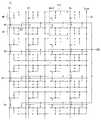
도 3은 도 2에 도시된 표시패널의 픽셀 어레이를 간략히 보여주는 등가 회로도.
도 4는 2D 모드에서 게이트 로우 전압으로 발생되는 방전 제어전압을 보여주는 도면.
도 5는 3D 모드에서 발생되는 방전 제어전압을 보여주는 도면.
도 6은 도 2 및 도 3에 도시된 픽셀의 접속 구성을 상세히 보여주는 등가 회로도.
도 7은 각 구동 모드에서 픽셀의 충전 및 방전 파형을 보여주는 도면.
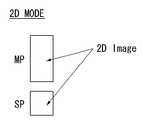
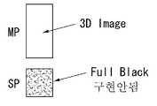
도 8은 및 도 9는 각각 2D 모드 및 3D 모드에서 보조 표시부의 동작을 보여주는 도면들.
도 10은 방전 제어라인이 표시패널에 형성되는 일 예를 보여주는 도면.
도 11은 방전 제어라인의 라인 저항으로 인해 위치별로 방전 제어전압이 달라지는 것을 보여주는 도면.
도 12는 방전 제어전압의 감쇄가 가장 큰 픽셀에서의 3D 표시상태를 보여주는 도면.
도 13은 방전 제어전압을 보상하기 위한 방전제어전압 발생회로의 세부 구성을 보여주는 도면.
도 14는 도 13에 도시된 제어전압 보상부의 일 예를 보여주는 도면.
도 15는 도 13에 도시된 제어전압 보상부의 다른 예를 보여주는 도면.
도 16은 제어전압 보상부와 표시패널의 픽셀들 간 접속 관계를 보여주는 도면.BRIEF DESCRIPTION OF THE DRAWINGS FIG. 1 is a perspective view of a stereoscopic image display apparatus according to an embodiment of the present invention; FIG.
3 is an equivalent circuit diagram schematically showing a pixel array of the display panel shown in Fig.
4 is a diagram showing a discharge control voltage generated at a gate-low voltage in a 2D mode;
5 is a view showing a discharge control voltage generated in the 3D mode;
Fig. 6 is an equivalent circuit diagram showing the connection configuration of the pixel shown in Figs. 2 and 3 in detail; Fig.
7 shows charge and discharge waveforms of a pixel in each drive mode;
FIG. 8 and FIG. 9 are views showing the operation of the auxiliary display unit in the 2D mode and the 3D mode, respectively.
10 is a view showing an example in which a discharge control line is formed on a display panel;
11 is a view showing that a discharge control voltage varies depending on a position due to a line resistance of a discharge control line.
12 is a view showing a 3D display state at a pixel with the largest attenuation of the discharge control voltage.
13 is a diagram showing a detailed configuration of a discharge control voltage generating circuit for compensating a discharge control voltage.
14 is a diagram showing an example of the control voltage compensating unit shown in FIG. 13;
15 is a view showing another example of the control voltage compensating portion shown in FIG. 13;
16 is a view showing a connection relationship between the control voltage compensating unit and the pixels of the display panel.
이하, 도 1 내지 도 16을 참조하여 본 발명의 바람직한 실시예에 대하여 상세히 설명하기로 한다.Hereinafter, preferred embodiments of the present invention will be described in detail with reference to FIGS. 1 to 16. FIG.
도 1 및 도 2는 본 발명의 실시예에 따른 편광 안경방식의 입체 영상 표시장치를 보여준다. 그리고, 도 3은 도 2에 도시된 표시패널의 픽셀 어레이를 간략히 보여 준다. 도 3에서, D1~Dm은 데이터라인을, G1~Gn은 게이트라인을 각각 지시한다.FIG. 1 and FIG. 2 show a polarizing glasses type stereoscopic image display apparatus according to an embodiment of the present invention. 3 schematically shows a pixel array of the display panel shown in Fig. In Fig. 3, D1 to Dm denote data lines and G1 to Gn denote gate lines, respectively.
도 1 내지 도 3을 참조하면, 이 입체 영상 표시장치는 표시소자(10), 패턴드 리타더(20), 콘트롤러(30), 패널 구동회로(40) 및 편광 안경(50)을 구비한다.1 to 3, the stereoscopic image display device includes a
표시소자(10)는 액정표시소자(Liquid Crystal Display, LCD), 전계 방출 표시소자(Field Emission Display, FED), 플라즈마 디스플레이 패널(Plasma Display Panel, PDP), 및 무기 전계발광소자와 유기발광다이오드소자(Organic Light Emitting Diode, OLED)를 포함한 전계발광소자(Electroluminescence Device, EL), 전기영동 표시소자(Electrophoresis, EPD) 등의 평판 표시소자로 구현될 수 있다. 이하에서, 표시소자(10)를 액정표시소자를 중심으로 설명한다.The
표시소자(10)는 표시패널(11)과, 상부 편광필름(Polarizer)(11a)과, 하부 편광필름(11b)을 포함한다.The
표시패널(11)은 2D 모드에서 2D 영상을 표시하고, 3D 모드에서 3D 영상을 표시한다. 표시패널(11)은 두 장의 유리기판들과 이들 사이에 형성된 액정층을 포함한다. 표시패널(11)의 하부 유리기판에는 다수의 데이터라인들(DL), 이 데이터라인들(DL)과 각각 교차되는 다수의 게이트라인들(GL), 공통전압(Vcom)이 공급되는 공통라인(CL), 방전 제어전압(V3D)이 공급되는 방전 제어라인(CONL)이 형성된다.The
표시패널(11)의 상부 유리기판 상에는 블랙매트릭스, 컬러필터가 형성된다. 표시패널(11)의 상부 유리기판과 하부 유리기판 각각에는 상부 및 하부 편광필름(11a, 11b)이 부착되고 액정의 프리틸트각(pre-tilt angle)을 설정하기 위한 배향막이 형성된다. 공통전압(Vcom)이 공급되는 공통전극은 TN(Twisted Nematic) 모드와 VA(Vertical Alignment) 모드와 같은 수직전계 구동방식에서 상부 유리기판 상에 형성될 수 있으며, IPS(In Plane Switching) 모드와 FFS(Fringe Field Switching) 모드와 같은 수평전계 구동방식에서 화소전극과 함께 하부 유리기판 상에 형성될 수 있다. 유리기판들 사이에는 액정셀의 셀갭(Cell gap)을 유지하기 위한 컬럼 스페이서가 형성될 수 있다.On the upper glass substrate of the
이러한 본 발명의 표시소자(10)는 투과형 표시소자, 반투과형 표시소자, 반사형 표시소자 등 어떠한 형태로도 구현될 수 있다. 투과형 표시소자와 반투과형 표시소자에서는 백라이트 유닛(12)이 필요하다. 백라이트 유닛(12)은 직하형(direct type) 백라이트 유닛 또는, 에지형(edge type) 백라이트 유닛으로 구현될 수 있다.The
신호라인들(DL,GL)의 교차 구조에 의해 표시패널(11)에는 다수의 단위 픽셀들을 포함한 픽셀 어레이가 형성된다. 단위 픽셀은 각각 적색(R), 녹색(G) 및 청색(B) 구현을 위한 3개의 픽셀들(PIX)을 구비한다. 픽셀들(PIX) 각각은 도 3과 같이 메인 표시부(MP)와 액티브 블랙 스트라이프로 기능하는 보조 표시부(SP)를 포함한다. 보조 표시부들(SP)은 방전 제어라인(CONL)에 공통으로 연결된다. 방전 제어라인(CONL)은 보조 표시부들(SP)의 방전 동작을 제어하기 위한 방전 제어전압(V3D)을 보조 표시부들(SP)의 방전 제어 TFT(DST)에 인가한다.A pixel array including a plurality of unit pixels is formed on the
메인 픽셀부(MP)는 2D 모드에서 2D 영상의 비디오 데이터를 표시하고, 3D 모드에서 3D 영상의 비디오 데이터를 표시한다. 이에 비하여, 보조 표시부(SP)는 2D 모드에서 2D 영상의 비디오 데이터를 표시하는 역할을 하는 반면, 3D 모드에서 블랙 계조를 표시하여 블랙 스트라이프 역할을 한다. 보조 표시부(SP)는 2D 모드에서 2D 영상의 개구율과 휘도를 높이고 3D 모드에서 3D 영상의 상하 시야각을 확대한다. 1 서브 픽셀 내에서 메인 픽셀부(MP)와 서브 표시부(SP)의 크기와 형태는 패널 구동 특성, 표시 영상의 휘도, 3D 영상의 시야각, 응용 제품 특성 등을 고려하여 적절히 설계될 수 있다.The main pixel unit MP displays the video data of the 2D image in the 2D mode and the video data of the 3D image in the 3D mode. On the other hand, the auxiliary display unit SP serves to display video data of a 2D image in the 2D mode, while displaying black gradation in the 3D mode to serve as a black stripe. The auxiliary display unit (SP) increases the aperture ratio and brightness of the 2D image in the 2D mode and enlarges the upper and lower viewing angles of the 3D image in the 3D mode. The sizes and shapes of the main pixel unit MP and the sub display unit SP within one subpixel can be appropriately designed in consideration of the panel driving characteristics, the brightness of the display image, the viewing angle of the 3D image, and the characteristics of the application product.
패턴드 리타더(20)는 표시패널(11)의 상부 편광필름(11a)에 부착된다. 패턴드 리타더(20)의 기수 라인들에는 제1 리타더(RT1)가 형성되고, 패턴드 리터더(20)의 우수 라인들에는 제2 리타더(RT2)가 형성된다. 제1 리타더(RT1)의 광흡수축과 제2 리타더(RT2)의 광흡수축은 서로 다르다. 패턴드 리타더(20)의 제1 리타더(RT1)는 픽셀 어레이의 기수번째 수평 픽셀라인과 대향하고, 제2 리타더(RT2)는 픽셀 어레이의 우수번째 수평 픽셀라인과 대향한다. 제1 리타더(RT1)는 상부 편광필름(11a)을 통해 입사되는 선편광의 위상을 1/4 파장 만큼 지연시켜 제1 편광(예컨대, 좌원편광)으로 통과시킨다. 제2 리타더(RT2)는 상부 편광필름(11a)을 통해 입사되는 선편광의 위상을 3/4 파장 만큼 지연시켜 제2 편광(예컨대, 우원편광)으로 통과시킨다.The patterned
콘트롤러(30)는 모드 선택신호(SEL)에 따라 2D 모드 또는 3D 모드로 패널 구동회로(40)의 동작을 제어한다. 콘트롤러(30)는 터치 스크린, 온 스크린 디스플레이(On screen display, OSD), 키보드, 마우스, 리모트 콘트롤러(Remote controller)와 같은 유저 인터페이스를 통해 모드 선택신호(SEL)를 입력받고, 그에 따라 2D 모드 동작과 3D 모드 동작을 전환할 수 있다. 한편, 콘트롤러(30)는 입력 영상의 데이터에 인코딩된 2D/3D 식별 코드 예를 들면, 디지털 방송 규격의 EPG(Electronic Program Guide) 또는 ESG(Electronic Service Guide)에 코딩될 수 있는 2D/3D 식별코드를 검출하여 2D 모드와 3D 모드를 구분할 수도 있다.The
콘트롤러(30)는 3D 모드 하에서 비디오 소스로부터 입력되는 3D 영상 데이터를 좌안 영상의 RGB 데이터와 우안 영상의 RGB 데이터로 분리한 후, 좌안 영상의 RGB 데이터와 우안 영상의 RGB 데이터를 데이터 드라이버(41)에 공급한다. 콘트롤러(30)는 2D 모드 하에서 비디오 소스로부터 입력되는 2D 영상의 RGB 데이터를 데이터 드라이버(41)에 공급한다.The
콘트롤러(30)는 수직 동기신호(Vsync), 수평 동기신호(Hsync), 데이터 인에이블 신호(Data Enable, DE), 도트 클럭(DCLK) 등의 타이밍신호들을 이용하여 패널 구동회로(40)의 동작 타이밍을 제어하기 위한 제어신호들을 발생한다.The
데이터 드라이버(41)의 동작 타이밍을 제어하기 위한 데이터 제어신호는 1 수평라인분의 데이터가 표시되는 1 수평기간 중에서 데이터의 시작점을 지시하는 소스 스타트 펄스(Source Start Pulse : SSP), 라이징(Rising) 또는 폴링(Falling) 에지에 기준하여 데이터의 래치동작을 제어하는 소스 샘플링 클럭(Source Sampling Clock : SSC), 데이터 드라이버(41)의 출력을 제어하는 소스 출력 인에이블신호(SOE), 및 표시패널(11)의 액정셀들에 공급될 데이터전압의 극성을 제어하는 극성제어신호(POL) 등을 포함한다.The data control signal for controlling the operation timing of the
게이트 드라이버(42)의 동작 타이밍을 제어하기 위한 게이트 제어신호는 한 화면이 표시되는 1 수직기간 중에서 스캔이 시작되는 시작 수평라인을 지시하는 게이트 스타트 펄스(Gate Start Pulse : GSP), 게이트 드라이버(42) 내의 쉬프트 레지스터에 입력되어 게이트 스타트 펄스(GSP)를 순차적으로 쉬프트시키기 위한 게이트 쉬프트 클럭신호(Gate Shift Clock : GSC), 및 게이트 드라이버(42)의 출력을 제어하는 게이트 출력 인에이블신호(Gate Output Enable : GOE) 등을 포함한다.The gate control signal for controlling the operation timing of the
콘트롤러(30)는 입력 프레임 주파수에 동기되는 타이밍신호들(Vsync,Hsync,DE,DCLK)을 체배하여 N×f(N은 2이상의 양의 정수, f는 입력 프레임 주파수)Hz의 프레임 주파수로 패널 구동회로(40)의 동작을 제어할 수 있다. 입력 프레임 주파수는 NTSC(National Television Standards Committee) 방식에서 60Hz이며, PAL(Phase-Alternating Line) 방식에서 50Hz이다.The
패널 구동회로(40)는 표시패널(11)의 데이터라인들(DL)을 구동시키기 위한 데이터 드라이버(41)와, 표시패널(11)의 게이트라인들(GL)을 구동시키기 위한 게이트 드라이버(42)와, 표시패널(11)의 방전 제어라인(CONL)을 구동시키기 위한 방전제어전압 발생회로(43)를 포함한다.The
데이터 드라이버(41)의 구동 IC들 각각은 쉬프트 레지스터(Shift register), 래치(Latch), 디지털-아날로그 변환기(Digital to Analog convertor, DAC), 출력 버퍼(Output buffer) 등을 포함한다. 데이터 드라이버(41)는 데이터 제어신호(SSP,SSC,SOE)에 따라 2D 또는 3D 영상의 RGB 데이터를 래치한다. 데이터 드라이버(41)는 극성제어신호(POL)에 응답하여 2D 또는 3D 영상의 RGB 데이터를 아날로그 정극성 감마보상전압과 부극성 감마보상전압으로 변환하여 데이터전압의 극성을 반전시킨다. 데이터 드라이버(41)는 게이트 드라이버(42)로부터 출력되는 스캔펄스(또는, 게이트펄스)에 동기되도록 데이터전압을 데이터라인들(DL)에 출력한다. 데이터 드라이버(41)의 구동 IC들은 TAB(Tape Automated Bonding) 공정에 의해 표시패널(11)의 하부 유리기판에 접합될 수 있다.Each of the driving ICs of the
게이트 드라이버(42)는 게이트 제어신호(GSP,GSC,GOE)에 따라 게이트 하이 전압과 게이트 로우 전압 사이에서 스윙되는 스캔펄스를 발생한다. 그리고, 게이트 제어신호(GSP,GSC,GOE)에 따라 스캔펄스를 게이트라인들(GL)에 라인 순차 방식으로 공급한다. 게이트 드라이버(42)는 게이트 쉬프트 레지스터 어레이(Gate shift register array)등을 포함한다. 게이트 드라이버(42)의 게이트 쉬프트 레지스터 어레이는 표시패널(11)에서 픽셀 어레이가 형성된 표시영역 바깥의 비 표시영역에 GIP(Gate In Panel) 방식으로 형성될 수 있다. GIP 방식에 의해, 게이트 쉬프트 레지스터들은 픽셀 어레이의 TFT(Thin Film Transistor) 공정에서 픽셀 어레이와 함께 형성될 수 있다. 게이트 드라이버(42)의 게이트 쉬프트 레지스터 어레이는 TAB 공정에 의해 표시패널(11)의 하부 유리기판에 접합되는 구동 IC들로 구현될 수도 있다.The
방전제어전압 발생회로(43)는 모드 선택신호(SEL)에 따라 방전 제어전압(V3D)을 서로 다르게 발생한다. 2D 모드에서 방전 제어전압(V3D)은 게이트 로우 전압과 실질적으로 동일한 레벨로 발생될 수 있다. 3D 모드에서 방전 제어전압(V3D)는 게이트 로우 전압보다 높고 게이트 하이 전압보다 낮은 슬라이트-온 레벨로 발생되되 주기적으로 게이트 로우 전압으로 낮아질 수 있다.The discharge control
편광 안경(50)은 좌안 편광필터를 갖는 좌안(50L)과 우안 편광필터를 갖는 우안(50R)을 구비한다. 좌안 편광필터는 패턴드 리타더(20)의 제1 리타더(RT1)와 동일한 광흡수축을 가지며, 우안 편광필터는 패턴드 리타더(20)의 제2 리타더(RT2)와 동일한 광흡수축을 가진다. 예들 들면, 편광 안경(50)의 좌안 편광필터는 좌원편광 필터로 선택될 수 있고, 편광 안경(50)의 우안 편광필터는 우원편광 필터로 선택될 수 있다. 사용자는 편광 안경(50)을 통해 표시소자(10)에 공간분할 방식으로 표시된 3D 영상 데이터를 감상할 수 있다.The
도 4는 2D 모드에서 발생되는 방전 제어전압(V3D)을 나타내고, 도 5는 3D 모드에서 발생되는 방전 제어전압(V3D)을 나타낸다.Fig. 4 shows the discharge control voltage V3D generated in the 2D mode, and Fig. 5 shows the discharge control voltage V3D generated in the 3D mode.
도 4 및 도 5를 참조하면, 방전 제어전압(V3D)은 2D 모드에서 스캔펄스(SCAN)의 게이트 로우 전압(VGL)과 동일 레벨로 발생될 수 있다. 표시패널(11)의 스위치들(도 6의 ST1,ST2)을 오프(off)시킬 수 있는 스캔펄스(SCAN)의 게이트 로우 전압(VGL)이 -5V로 선택되는 경우, 2D용 제어전압(V2D)은 -5V로 발생될 수 있다.4 and 5, the discharge control voltage V3D may be generated at the same level as the gate-low voltage VGL of the scan pulse SCAN in the 2D mode. When the gate low voltage VGL of the scan pulse SCAN capable of turning off the switches (ST1 and ST2 in Fig. 6) of the
방전 제어전압(V3D)은 3D 모드에서 슬라이트-온 레벨(SOL)로 발생되되, 방전 제어 스위치의 포지티브 게이트-바이어스 스트레스(positive gate-bias stress)가 줄어들도록 일정 주기로 게이트 로우 전압(VGL)으로 낮아질 수 있다. 슬라이트-온 레벨(SOL)은 방전 과정에서 킥백(kick-back) 전압의 영향을 최소화하기 위해 공통전압(Vcom)보다 높고 스캔펄스(SCAN)의 게이트 하이 전압(VGH)보다 낮게 설정될 수 있다. 표시패널(11)의 스위치들을 풀-온(full-on) 시킬 수 있는 스캔펄스(SCAN)의 게이트 하이 전압(VGH)이 28V로 선택되고 공통전압(Vcom)이 7.5V로 선택되는 경우, 슬라이트-온 레벨(SOL)의 방전 제어전압(V3D)은 8V~12V로 발생될 수 있다.The discharge control voltage V3D is generated in the 3D mode at the slit-on level (SOL), and is gradually reduced to the gate-low voltage (VGL) so that the positive gate-bias stress of the discharge control switch is reduced Can be lowered. The slit-on level (SOL) may be set to be higher than the common voltage (Vcom) and lower than the gate high voltage (VGH) of the scan pulse (SCAN) in order to minimize the influence of the kick- . When the gate high voltage VGH of the scan pulse SCAN capable of full-on switching of the switches of the
3D 모드에서, 슬라이트-온 레벨(SOL)의 방전 제어전압(V3D)이 발생되는 기간은 각 프레임에서 유효 비디오 데이터가 표시되는 표시구간(AP)에 대응될 수 있고, 게이트 로우 전압(VGL)의 방전 제어전압(V3D)이 발생되는 기간은 이웃한 표시구간들(AP) 사이의 비 표시구간 즉, 수직 블랭크 구간(VB)에 대응될 수 있다. 다만, 3D 모드에서, 슬라이트-온 레벨(SOL)의 방전 제어전압(V3D)이 발생되는 기간은 최하단 수평 픽셀라인의 방전기간 확보를 위해 표시구간(AP)에 비해 넓어질 수 있다.In the 3D mode, the period during which the discharge control voltage V3D of the slew-on level SOL is generated may correspond to the display period AP in which valid video data is displayed in each frame, A period during which the discharge control voltage V3D of the display period AP is generated may correspond to a non-display period between the neighboring display periods AP, i.e., a vertical blank interval VB. However, in the 3D mode, the period during which the discharge control voltage V3D of the slit-on level SOL is generated may be wider than the display period AP for securing the discharge period of the lowermost horizontal pixel line.
도 6은 도 2 및 도 3에 도시된 픽셀(PIX)의 접속 구성을 상세히 보여준다.Fig. 6 shows the connection configuration of the pixel PIX shown in Figs. 2 and 3 in detail.
도 6을 참조하면, 메인 표시부(MP)는 제1 화소전극(Ep1), 이 제1 화소전극(Ep1)과 대향하여 제1 액정 커패시터(Clc1)를 구성하는 제1 공통전극(Ec1), 및 제1 스토리지 커패시터(Cst1)를 구비한다. 제1 화소전극(Ep1)은 제1 스위치(ST1)를 통해 데이터라인(DL)에 연결된다. 제1 스위치(ST1)는 스캔펄스(SCAN)에 응답하여 턴 온 됨으로써 데이터라인(DL) 상의 데이터전압(Vdata)을 제1 화소전극(Ep1)에 인가한다. 제1 스위치(ST1)의 게이트전극은 게이트라인(GL)에 접속되고, 소스전극은 데이터라인(DL)에 접속되며, 드레인전극은 제1 화소전극(Ep1)에 접속된다. 제1 공통전극(Ec1)은 공통전압(Vcom)으로 충전된 공통라인(CL)에 접속된다. 제1 스토리지 커패시터(Cst1)는 절연층을 사이에 두고 제1 화소전극(Ep1)과 공통라인(CL)의 중첩으로 형성된다.Referring to FIG. 6, the main display unit MP includes a first pixel electrode Ep1, a first common electrode Ec1 constituting a first liquid crystal capacitor Clc1 opposite to the first pixel electrode Ep1, And a first storage capacitor Cst1. The first pixel electrode Ep1 is connected to the data line DL through the first switch ST1. The first switch ST1 applies a data voltage Vdata on the data line DL to the first pixel electrode Ep1 by being turned on in response to the scan pulse SCAN. The gate electrode of the first switch ST1 is connected to the gate line GL, the source electrode thereof is connected to the data line DL, and the drain electrode thereof is connected to the first pixel electrode Ep1. The first common electrode Ec1 is connected to the common line CL charged with the common voltage Vcom. The first storage capacitor Cst1 is formed by overlapping the first pixel electrode Ep1 and the common line CL with an insulating layer interposed therebetween.
보조 표시부(SP)는 제2 화소전극(Ep2), 이 제2 화소전극(Ep2)과 대향하여 제2 액정 커패시터(Clc2)를 구성하는 제2 공통전극(Ec2), 및 제2 스토리지 커패시터(Cst2)를 구비한다. 제2 화소전극(Ep2)은 제2 스위치(ST2)를 통해 데이터라인(DL)에 연결된다. 제2 스위치(ST2)는 스캔펄스(SCAN)에 응답하여 턴 온 됨으로써 데이터라인(DL) 상의 데이터전압(Vdata)을 제2 화소전극(Ep2)에 인가한다. 제2 스위치(ST2)의 게이트전극은 게이트라인(GL)에 접속되고, 소스전극은 데이터라인(DL)에 접속되며, 드레인전극은 제2 화소전극(Ep2)에 접속된다. 제2 공통전극(Ec2)은 공통전압(Vcom)으로 충전된 공통라인(CL)에 접속된다. 제2 스토리지 커패시터(Cst2)는 절연층을 사이에 두고 제2 화소전극(Ep2)과 공통라인(CL)의 중첩으로 형성된다.The auxiliary display unit SP includes a second pixel electrode Ep2, a second common electrode Ec2 constituting a second liquid crystal capacitor Clc2 opposite to the second pixel electrode Ep2, and a second common electrode Ec2 constituting a second storage capacitor Cst2 . And the second pixel electrode Ep2 is connected to the data line DL through the second switch ST2. The second switch ST2 applies a data voltage Vdata on the data line DL to the second pixel electrode Ep2 by being turned on in response to the scan pulse SCAN. The gate electrode of the second switch ST2 is connected to the gate line GL, the source electrode thereof is connected to the data line DL, and the drain electrode thereof is connected to the second pixel electrode Ep2. And the second common electrode Ec2 is connected to the common line CL charged with the common voltage Vcom. The second storage capacitor Cst2 is formed by overlapping the second pixel electrode Ep2 and the common line CL with the insulating layer interposed therebetween.
제2 화소전극(Ep2)은 방전제어 스위치(DST)를 통해 공통라인(CL)에 연결된다. 방전제어 스위치(DST)는 방전 제어전압(V3D)에 응답하여 제2 화소전극(Ep2)과 공통라인(CL) 사이의 전류 패스를 스위칭한다. 방전제어 스위치(DST)의 게이트전극은 방전 제어라인(CONL)에 접속되고, 소스전극은 제2 화소전극(Ep2)에 접속되며, 드레인전극은 공통라인(CL)에 접속된다. 방전 제어전압(V3D)이 게이트 로우 전압(VGL)으로 인가될 때, 방전제어 스위치(DST)는 자신의 소스-드레인 간 채널을 완전히 폐쇄하여 제2 화소전극(Ep2)과 공통라인(CL) 사이의 전류 패스를 차단한다. 슬라이트-온 레벨(SOL)의 방전 제어전압(V3D)이 인가될 때, 방전제어 스위치(DST)는 자신의 소스-드레인 간 채널을 부분 개방하여 제2 화소전극(Ep2)과 공통라인(CL) 사이의 전류 패스를 부분적으로 허여한다.And the second pixel electrode Ep2 is connected to the common line CL through the discharge control switch DST. The discharge control switch DST switches the current path between the second pixel electrode Ep2 and the common line CL in response to the discharge control voltage V3D. The gate electrode of the discharge control switch DST is connected to the discharge control line CONL, the source electrode thereof is connected to the second pixel electrode Ep2, and the drain electrode thereof is connected to the common line CL. When the discharge control voltage V3D is applied to the gate-low voltage VGL, the discharge control switch DST completely closes the source-drain channel of the discharge control switch DST so that the second pixel electrode Ep2 and the common line CL Of the current path. When the discharge control voltage V3D of the slit-on level SOL is applied, the discharge control switch DST partially opens the source-drain channel of the discharge control switch DST to the second pixel electrode Ep2 and the common line CL Lt; RTI ID = 0.0 > partly < / RTI >
방전제어 스위치(DST)는 제1 및 제2 스위치(ST1,ST2)와 동일한 채널 용량을 갖도록 설계된다. 따라서, 방전제어 스위치(DST)는 게이트 하이 전압(VGH)에 비해 낮은 슬라이트-온 레벨(SOL)의 방전 제어전압(V3D)이 인가됨에 따라, 풀 온 레벨(full on level) 보다 낮은 슬라이트 온 레벨(slight on level)로 도통된다. 제2 스위치(ST2)와 방전제어 스위치(DST)가 동시에 온 되더라도, 방전제어 스위치(DST)를 통해 흐르는 전류량은 제2 스위치(ST2)를 통해 흐르는 전류량에 비해 적다. 채널 저항은 게이트전극에 인가되는 전압에 반비례하기 때문에, 제2 스위치(ST2)와 방전제어 스위치(DST)가 동시에 온 되더라도, 방전제어 스위치(DST)의 채널 저항은 제2 스위치(ST2)의 채널 저항에 비해 크다.The discharge control switch DST is designed to have the same channel capacity as the first and second switches ST1 and ST2. Therefore, the discharge control switch DST is turned on and off in response to the application of the discharge control voltage V3D of the lower slit-on level SOL to the gate high voltage VGH, And is conducted at a slight on level. Even if the second switch ST2 and the discharge control switch DST are turned on at the same time, the amount of current flowing through the discharge control switch DST is smaller than the amount of current flowing through the second switch ST2. Since the channel resistance is inversely proportional to the voltage applied to the gate electrode, even if the second switch ST2 and the discharge control switch DST are turned on at the same time, the channel resistance of the discharge control switch DST becomes equal to the channel of the second switch ST2 It is larger than the resistance.
도 7은 각 구동 모드에서 픽셀(PIX)의 충전 및 방전 파형을 보여준다. 도 8은 및 도 9는 각각 2D 모드 및 3D 모드에서 보조 표시부의 동작을 보여준다.FIG. 7 shows charge and discharge waveforms of the pixel PIX in each drive mode. FIG. 8 and FIG. 9 show the operation of the auxiliary display unit in the 2D mode and the 3D mode, respectively.
도 7 내지 도 9를 참조하여 각 구동 모드에서 픽셀(PIX)의 동작과 함께 그의 작용 효과를 설명하면 다음과 같다.7 to 9, the operation of the pixel PIX in each driving mode as well as its effect will be described below.
먼저 2D 모드에서의 동작을 설명하면,First, the operation in the 2D mode will be described.
방전제어 스위치(DST)는 게이트 로우 전압(VGL)의 방전 제어전압(V3D)에 응답하여 T1 및 T2 기간 동안 계속해서 턴 오프 상태를 유지한다.The discharge control switch DST maintains the turn-off state for the periods T1 and T2 in response to the discharge control voltage V3D of the gate-low voltage VGL.
T1 기간 동안, 게이트 하이 전압(VGH)의 스캔펄스(SCAN)에 응답하여 제1 및 제2 스위치(ST1,ST2)는 동시에 풀-온 레벨로 턴 온 된다.During the period T1, the first and second switches ST1 and ST2 are simultaneously turned on to the pull-on level in response to the scan pulse SCAN of the gate high voltage VGH.
제1 스위치(ST1)의 턴 온에 의해 메인 표시부(MP)의 제1 화소전극(Ep1)에는 2D 영상 구현을 위한 데이터전압(Vdata)이 제1 화소전압(Vp1)으로 충전되고, 제2 스위치(ST2)의 턴 온에 의해 보조 표시부(SP)의 제2 화소전극(Ep2)에도 마찬가지로 2D 영상 구현을 위한 동일한 데이터전압(Vdata)이 제2 화소전압(Vp2)으로 충전된다. 제1 및 제2 스위치(ST1,ST2)는 동일하게 설계되기 때문에, 제2 화소전압(Vp2)은 제1 화소전압(Vp1)과 실질적으로 동일하다.The data voltage Vdata for realizing the 2D image is charged to the first pixel voltage Vp1 in the first pixel electrode Ep1 of the main display unit MP by turning on the first switch ST1, The same data voltage Vdata for realizing a 2D image is similarly charged to the second pixel electrode Vp2 on the second pixel electrode Ep2 of the auxiliary display portion SP by turning on the second pixel voltage Vp2. Since the first and second switches ST1 and ST2 are designed in the same manner, the second pixel voltage Vp2 is substantially equal to the first pixel voltage Vp1.
T2 기간 동안, 게이트 로우 전압(VGL)의 스캔펄스(SCAN)에 응답하여 제1 및 제2 스위치(ST1,ST2)는 동시에 턴 오프 된다.During the period T2, the first and second switches ST1 and ST2 are simultaneously turned off in response to the scan pulse SCAN of the gate low voltage VGL.
제1 스위치(ST1)의 턴 오프에 의해, 메인 표시부(MP)의 제1 화소전극(Ep1)에 충전되어 있던 제1 화소전압(Vp1)은 킥백 전압의 영향으로 소정값만큼 쉬프트되고, 제1 스토리지 커패시터(Cst1)에 의해 이 쉬프트 된 값으로 유지된다. 제2 스위치(ST2)의 턴 오프에 의해, 보조 표시부(SP)의 제2 화소전극(Ep2)에 충전되어 있던 제2 화소전압(Vp2)은 킥백 전압의 영향으로 소정값만큼 쉬프트되고, 제2 스토리지 커패시터(Cst2)에 의해 이 쉬프트 된 값으로 유지된다.The first pixel voltage Vp1 charged in the first pixel electrode Ep1 of the main display unit MP is shifted by a predetermined value under the influence of the kickback voltage due to the turn-off of the first switch ST1, And is held at this shifted value by the storage capacitor Cst1. The second pixel voltage Vp2 charged in the second pixel electrode Ep2 of the auxiliary display unit SP is shifted by a predetermined value due to the effect of the kickback voltage due to the turn-off of the second switch ST2, And is held at this shifted value by the storage capacitor Cst2.
한편, T1 및 T2 기간에서 메인 표시부(MP)의 제1 공통전극(Ec1)과 보조 표시부(SP)의 제2 공통전극(Ec2)에는 공통라인(CL)을 통해 공통전압(Vcom)이 인가되고 있다. 제1 화소전압(Vp1)과 공통전압(Vcom) 간 전압차는 제2 화소전압(Vp2)과 공통전압(Vcom) 간 전압차와 동일하게 유지된다. 노멀리 블랙(normaly black)의 액정 모드에서 액정셀의 투과율은 화소전극과 공통전극 간 전위차에 비례한다. 그 결과, 메인 표시부(MP)와 보조 표시부(SP)는 도 8과 같이 동일 계조의 2D 영상을 구현하게 된다. 여기서, 보조 표시부(SP)에 표시되는 2D 이미지는 2D 영상의 휘도를 높이는 역할을 한다.On the other hand, in the periods T1 and T2, the common voltage Vcom is applied to the first common electrode Ec1 of the main display unit MP and the second common electrode Ec2 of the auxiliary display unit SP through the common line CL have. The voltage difference between the first pixel voltage Vp1 and the common voltage Vcom is maintained equal to the voltage difference between the second pixel voltage Vp2 and the common voltage Vcom. The transmittance of the liquid crystal cell in the liquid crystal mode of normaly black is proportional to the potential difference between the pixel electrode and the common electrode. As a result, the main display unit MP and the auxiliary display unit SP implement a 2D image of the same gradation as shown in FIG. Here, the 2D image displayed on the auxiliary display unit SP serves to increase the luminance of the 2D image.
다음으로 3D 모드 하에서의 동작을 설명하면,Next, the operation in the 3D mode will be described.
방전제어 스위치(DST)는 방전 제어전압(V3D)에 응답하여 소정 주기로 슬라이트-온 레벨의 온 상태와, 오프 상태를 반복한다. 예컨대, 방전제어 스위치(DST)는 표시기간 동안 슬라이트-온 레벨의 온 상태를 유지하고, 표시기간들 사이의 수직 블랭크기간 동안 오프 상태를 유지한다. 이하의 T1 기간 및 T2 기간은 표시기간에 속한다.The discharge control switch DST repeats the on-state and off-state of the slit-on level in a predetermined cycle in response to the discharge control voltage V3D. For example, the discharge control switch DST maintains the on-state of the slit-on level during the display period and maintains the off state during the vertical blank period between the display periods. The following T1 period and T2 period belong to the display period.
T1 기간 동안, 게이트 하이 전압(VGH)의 스캔펄스(SCAN)에 응답하여 제1 및 제2 스위치(ST1,ST2)는 동시에 풀-온 레벨로 턴 온 된다.During the period T1, the first and second switches ST1 and ST2 are simultaneously turned on to the pull-on level in response to the scan pulse SCAN of the gate high voltage VGH.
제1 스위치(ST1)의 턴 온에 의해 메인 표시부(MP)의 제1 화소전극(Ep1)에는 3D 영상 구현을 위한 데이터전압(Vdata)이 제1 화소전압(Vp1)으로 충전되고, 제2 스위치(ST2)의 턴 온에 의해 보조 표시부(SP)의 제2 화소전극(Ep2)에도 마찬가지로 3D 영상 구현을 위한 동일한 데이터전압(Vdata)이 제2 화소전압(Vp2)으로 충전된다. T1 기간에서, 풀-온 레벨의 온 상태를 갖는 제2 스위치(ST2)의 채널저항에 비해, 슬라이트-온 레벨의 온 상태를 갖는 방전제어 스위치(DST)의 채널저항은 훨씬 크다. 그 결과, 제2 화소전극(Ep2)으로부터 유출되는 방전 전류는 제2 화소전극(Ep2)으로 유입되는 충전 전류에 비해 훨씬 적게 된다. 따라서, T1 기간 동안 슬라이트-온 레벨의 온 상태를 갖는 방전제어 스위치(DST)는 제2 화소전압(Vp2)의 충전 특성에 거의 영향을 주지 않게 되고, 그 결과 제2 화소전압(Vp2)은 제1 화소전압(Vp1)에 유사한 레벨로 충전된다.The data voltage Vdata for realizing the 3D image is charged to the first pixel voltage Vp1 in the first pixel electrode Ep1 of the main display unit MP by turning on the first switch ST1, The same data voltage Vdata for realizing a 3D image is similarly charged to the second pixel electrode Vp2 on the second pixel electrode Ep2 of the auxiliary display unit SP by the turn-on of the second pixel electrode ST2. In the T1 period, the channel resistance of the discharge control switch DST having the ON state of the slit-on level is much larger than the channel resistance of the second switch ST2 having the ON state of the pull-on level. As a result, the discharge current flowing out from the second pixel electrode Ep2 becomes much smaller than the charge current flowing into the second pixel electrode Ep2. Therefore, the discharge control switch DST having the on-state of the slit-on level during the period T1 does not substantially affect the charging characteristic of the second pixel voltage Vp2, and as a result, the second pixel voltage Vp2 And is charged to a level similar to the first pixel voltage Vp1.
T2 기간 동안, 게이트 로우 전압(VGL)의 스캔펄스(SCAN)에 응답하여 제1 및 제2 스위치(ST1,ST2)는 동시에 턴 오프 된다.During the period T2, the first and second switches ST1 and ST2 are simultaneously turned off in response to the scan pulse SCAN of the gate low voltage VGL.
제1 스위치(ST1)의 턴 오프에 의해, 메인 표시부(MP)의 제1 화소전극(Ep1)에 충전되어 있던 제1 화소전압(Vp1)은 킥백 전압의 영향으로 소정값만큼 쉬프트되고, 제1 스토리지 커패시터(Cst1)에 의해 이 쉬프트 된 값으로 유지된다. 제2 스위치(ST2)의 턴 오프 되면, 보조 표시부(SP)의 제2 화소전극(Ep2)에 충전되어 있던 제2 화소전압(Vp2)은 방전제어 스위치(DST)를 경유하여 유출되는 방전 전류에 의해 소정 기간 내에 공통전압(Vcom) 레벨로 방전된다. 오프 상태를 갖는 제2 스위치(ST2)의 채널저항에 비해, 슬라이트-온 레벨의 온 상태를 갖는 방전제어 스위치(DST)의 채널저항은 훨씬 작다. 그 결과, 방전제어 스위치(DST)를 통해 제2 화소전극(Ep2)에 충전되어 있던 제2 화소전압(Vp2)은 서서히 방전되어 킥백 전압의 영향 없이 공통전압(Vcom) 레벨에 수렴된다.The first pixel voltage Vp1 charged in the first pixel electrode Ep1 of the main display unit MP is shifted by a predetermined value under the influence of the kickback voltage due to the turn-off of the first switch ST1, And is held at this shifted value by the storage capacitor Cst1. When the second switch ST2 is turned off, the second pixel voltage Vp2 charged in the second pixel electrode Ep2 of the auxiliary display unit SP is supplied to the discharging current flowing out via the discharging control switch DST To a common voltage (Vcom) level within a predetermined period. The channel resistance of the discharge control switch DST having the ON state of the slit-on level is much smaller than the channel resistance of the second switch ST2 having the OFF state. As a result, the second pixel voltage Vp2 charged in the second pixel electrode Ep2 through the discharge control switch DST is gradually discharged and converged to the common voltage Vcom level without being affected by the kickback voltage.
한편, T1 및 T2 기간에서 메인 표시부(MP)의 제1 공통전극(Ec1)과 보조 표시부(SP)의 제2 공통전극(Ec2)에는 공통전압(Vcom)이 인가되고 있다. 제2 화소전압(Vp2)의 방전이 완료된 시점에서, 제1 화소전압(Vp1)과 공통전압(Vcom) 간 전압차와 달리, 제2 화소전압(Vp2)과 공통전압(Vcom) 간 전압차는 "0"이 된다. 그 결과, 노멀리 블랙의 전위차-투과율 특성에 따라, 메인 표시부(MP)는 도 9와 같이 특정 계조의 3D 영상을 표시하게 되는 반면, 보조 표시부(SP)는 도 9와 같이 블랙 계조의 영상을 표시하여 블랙 스트라이프로 기능한다.The common voltage Vcom is applied to the first common electrode Ec1 of the main display unit MP and the second common electrode Ec2 of the auxiliary display unit SP during the periods T1 and T2. The voltage difference between the second pixel voltage Vp2 and the common voltage Vcom is different from the voltage difference between the first pixel voltage Vp1 and the common voltage Vcom when the discharge of the second pixel voltage Vp2 is completed, 0 ". As a result, according to the potential difference-transmittance characteristic of normally black, the main display unit MP displays a 3D image of a specific grayscale as shown in Fig. 9, while the sub display unit SP displays a black grayscale image as shown in Fig. And functions as a black stripe.
보조 표시부(SP)에 표시되는 블랙 이미지는 수직으로 이웃한 3D 이미지들(즉, 좌안 이미지와 우안 이미지) 사이의 표시 간격을 넓히는 역할을 한다. 이에 따라, 별도의 블랙 스트라이프 패턴 없이도 크로스토크(Crosstalk)가 발생되지 않는 3D 상하 시야각이 상기 블랙 이미지를 통해 넓게 확보될 수 있게 된다.The black image displayed on the auxiliary display unit SP serves to widen the display interval between the vertically neighboring 3D images (i.e., the left-eye image and the right-eye image). Accordingly, a 3D vertical viewing angle in which crosstalk does not occur without a separate black stripe pattern can be ensured widely through the black image.
도 10은 방전 제어라인(CONL)이 표시패널(11)에 형성되는 일 예를 보여준다. 도 11은 방전 제어라인(CONL)의 라인 저항으로 인해 위치별로 방전 제어전압(V3D)이 달라지는 것을 보여준다. 도 12는 방전 제어전압(V3D)의 감쇄가 가장 큰 픽셀에서의 3D 표시상태를 보여준다.10 shows an example in which the discharge control line (CONL) is formed on the
도 10과 같이 표시패널(11)에 형성되는 방전 제어라인(CONL)은 전기적으로 연결되어 있다. 방전 제어라인(CONL)의 라인 저항은 방전 제어전압(V3D)의 입력 지점(IP)으로부터 멀어질수록 커진다. 도시된 바와 같이 방전 제어전압(V3D)이 표시패널(11)의 상단부에서 입력되는 경우, 방전 제어라인(CONL)의 라인 저항은 표시패널(11)의 하단부로 갈수록 점점 커진다.As shown in Fig. 10, the discharge control lines CONL formed on the
방전 제어전압(V3D)의 드롭량은 방전 제어라인(CONL)의 라인 저항에 비례하여 커진다. 따라서, 입력 지점(IP)으로부터 멀리 떨어진 픽셀에 공급되는 방전 제어전압(V3D)은 도 11과 같이 원하는 슬라이트-온 레벨(SOL)보다 낮은 레벨(SOL')로 떨어지게 된다.The drop amount of the discharge control voltage V3D increases in proportion to the line resistance of the discharge control line CONL. Therefore, the discharge control voltage V3D supplied to the pixel remote from the input point IP falls to the level (SOL ') lower than the desired slit-on level SOL as shown in FIG.
방전 제어전압(V3D)은 도 5와 같이 슬라이트-온 레벨(SOL)과 게이트 로우 전압(VGL) 사이에서 스윙되어야 하므로, 수직 블랭크 구간(VB)보다 짧은 시간 내에 보조 표시부(SP)의 방전이 완료되어야 한다. 방전 제어전압(V3D)이 슬라이트-온 레벨(SOL)보다 낮아지면 픽셀의 보조 표시부(SP)에 충전된 전압이 방전되는 시간은 미리 설계된 시간(통상 10 수평기간 ~ 15 수평기간)보다 길어진다. 따라서, 방전 제어전압(V3D)의 드롭량이 가장 큰 최하단 수평 픽셀라인에서 보조 표시부들(SP)은, 불충분한 방전 시간으로 인하여 완전한 블랙 계조의 구현이 어려워 도 12와 같이 블랙 스트라이프로 기능하기 어렵다.Since the discharge control voltage V3D has to be swung between the slit-on level SOL and the gate low voltage VGL as shown in Fig. 5, the discharge of the auxiliary display unit SP within a shorter time than the vertical blank period VB Should be completed. When the discharge control voltage V3D is lower than the slit-on level SOL, the time for discharging the charged voltage to the sub-display portion SP of the pixel becomes longer than the pre-designed time (usually 10 horizontal periods to 15 horizontal periods) . Therefore, in the lowermost horizontal pixel line in which the drop amount of the discharge control voltage V3D is the largest, it is difficult for the auxiliary display units SP to function as a black stripe as shown in FIG. 12 because of the difficulty in realizing a complete black gradation due to insufficient discharge time.
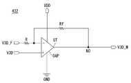
도 13은 방전 제어전압(V3D)을 보상하여 화면 전체의 보조 표시부들이 블랙 계조를 완전히 표현할 수 있도록 하는 방전제어전압 발생회로(43)의 세부 구성을 보여준다.FIG. 13 shows a detailed configuration of a discharge control
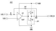
도 13을 참조하면, 방전제어전압 발생회로(43)는 제어전압 발생부(431)와 제어전압 보상부(432)를 구비한다. 제어전압 발생부(431)와 제어전압 보상부(432)는 3D 보드(100)에 실장될 수 있다.Referring to FIG. 13, the discharge control
제어전압 발생부(431)는 모드 선택신호(SEL)에 따라 방전 제어전압(V3D)을 서로 다르게 발생한다. 제어전압 발생부(431)는 파워 IC 및 레벨 쉬프터를 포함할 수 있다. 제어전압 발생부(431)는 2D 모드에서 파워 IC로부터 공급되는 입력 직류 전압을 레벨 쉬프팅하여 도 4와 같은 게이트 로우 전압(VGL)의 방전 제어전압(V3D)을 발생한다. 제어전압 발생부(431)는 3D 모드에서 콘트롤러(30)로부터 입력되는 극성제어신호(POL)와 소스 출력 인에이블신호(SOE) 등을 참조하여 하이 구간(도 5의 SOL 구간)과 로우 구간(도 5의 VGL 구간)을 포함하는 제어펄스를 발생하고, 파워 IC로부터 공급되는 입력 직류 전압을 이용하여 제어펄스를 레벨 쉬프팅하여 도 5와 같이 슬라이트-온 레벨(SOL)과 게이트 로우 전압(VGL)을 교번하는 방전 제어전압(V3D)을 발생한다.The control
제어전압 보상부(432)는 제어전압 발생부(431)로부터 방전 제어전압(V3D)을 입력받고, 이 입력 방전 제어전압(V3D)을 기준으로 표시패널(11)의 제1 측으로부터 공급되는 피드백 방전 제어전압(V3D_F)을 차동 증폭한 후, 이를 보상 방전 제어전압(V3D_M)으로서 제1 측과 반대되는 표시패널(11)의 제2 측에 인가한다. 여기서, 표시패널(11)의 제1 측은 제2 측에 비해 방전 제어라인의 라인 저항이 큰 영역으로서, 표시패널(11)의 최하단 수평 픽셀라인(도 16의 HL#n)에 해당될 수 있다. 이 경우, 표시패널(11)의 제2 측은 표시패널(11)의 최상단 수평 픽셀라인(도 16의 HL#1)에 해당된다.The control
최하단 수평 픽셀라인에서도 완전한 블랙 계조가 구현되도록, 보상 방전 제어전압(V3D_M)의 슬라이트-온 레벨(SOL)은 차동 증폭을 통해 입력 방전 제어전압(V3D)의 슬라이트-온 레벨(SOL)보다 높아진다.The level SL of the compensation discharge control voltage V3D_M is higher than the level SL of the input discharge control voltage V3D through the differential amplification so that full black gradation can be realized even in the lowermost horizontal pixel line. .
도 14는 도 13에 도시된 제어전압 보상부(432)의 일 예를 보여준다.FIG. 14 shows an example of the
도 14를 참조하면, 제어전압 보상부(432)는 오피 엠프(OAP)로 구현될 수 있다. 오피 엠프(OAP)는 입력 저항(R)을 통해 피드백 방전 제어전압(V3D_F)이 입력되는 반전 입력단(-)과, 입력 방전 제어전압(V3D)이 입력되는 비반전 입력단(+)과, 피드백 저항(Rf)을 통해 반전 입력단(-)에 접속되어 보상 방전 제어전압(V3D_M)을 출력하는 출력단(OT)을 포함한다. 출력단(OT)은 출력 노드(NO)를 통해 보상 방전 제어전압(V3D_M)을 출력한다.Referring to FIG. 14, the
오피 엠프(OAP)는 입력 방전 제어전압(V3D)과 피드백 방전 제어전압(V3D_F)의 차신호를 입력 저항(R)과 피드백 저항(Rf)에 따라 결정되는 반전 증폭률(-Rf/R)에 따라 증폭하여 보상 방전 제어전압(V3D_M)을 출력한다.The operational amplifier OAP changes the difference between the input discharge control voltage V3D and the feedback discharge control voltage V3D_F according to the inverting amplification factor -Rf / R determined by the input resistor R and the feedback resistor Rf And outputs the compensation discharge control voltage V3D_M.
도 15는 도 13에 도시된 제어전압 보상부(432)의 다른 예를 보여준다.Fig. 15 shows another example of the
도 15를 참조하면, 제어전압 보상부(432)는 도 15와 같은 오피 엠프(OAP)외에 푸쉬-풀(push-pull) 증폭기(PP)를 더 포함할 수 있다.15, the control
오피 엠프(OAP)의 구성 및 동작은 도 15에서 설명한 것과 실질적으로 동일하다.The configuration and operation of the operational amplifier (OAP) are substantially the same as those described in Fig.
푸쉬-풀 증폭기(PP)는 오피 엠프(OAP)의 출력단(OT)과 출력 노드(NO) 사이에 접속되어 보상 방전 제어전압(V3D_M)의 크기를 높이는 기능을 한다.The push-pull amplifier PP is connected between the output terminal OT of the op-amp OAP and the output node NO to increase the size of the compensation discharge control voltage V3D_M.
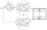
푸쉬-풀 증폭기(PP)는 오피 엠프(OAP)의 출력단(OT)에 걸리는 전압에 의해 공통으로 제어되며 고전위 전압원(VDD)과 기저 전압원(GND) 사이에 직렬 접속된 2개의 에미터 플로어(emitter follower)를 포함한다. 푸쉬-풀 증폭기(PP)는 오피 엠프(OAP)의 출력단(OT)에 걸리는 입력신호에 의해 제어되며 고전위 전압원(VDD)과 출력 노드(NO) 사이에 접속되어 입력신호의 양의 주기에서 도통되는 npn 트랜지스터(Q1)과, 오피 엠프(OAP)의 출력단(OT)에 걸리는 입력신호에 의해 제어되며 출력 노드(NO)와 기저 전압원(GND) 사이에 접속되어 입력신호의 음의 주기에서 도통되는 pnp 트랜지스터(Q2)로 구현된다.The push-pull amplifier PP is commonly controlled by the voltage applied to the output terminal OT of the operational amplifier OAP and has two emitter floors connected in series between the high potential power supply VDD and the ground voltage source GND emitter follower. The push-pull amplifier PP is controlled by an input signal applied to the output terminal OT of the operational amplifier OAP and is connected between the high potential voltage source VDD and the output node NO, And is connected between the output node NO and the ground voltage source GND and is made conductive in the negative period of the input signal. The npn transistor Q1 is connected to the output node OT of the operational amplifier OAP, and is implemented as a pnp transistor Q2.
도 16은 제어전압 보상부(432)와 표시패널(11)의 픽셀들 간 접속 관계를 보여준다. 도 16에서, HL#1~HL#n은 다수의 픽셀들을 각각 포함한 수평 픽셀라인을 지시한다.16 shows the connection relationship between the pixels of the control
도 16을 참조하면, 보상 방전 제어전압(V3D_M)이 출력되는 제어전압 보상부(432)의 출력단(NO)은, 최상단 수평 픽셀라인(HL#1)의 픽셀들에 접속된 방전 제어라인(CONL)을 입력 지점으로 하여 그에 연결된다.16, the output terminal NO of the control
피드백 방전 제어전압(V3D_F)이 입력되는 제어전압 보상부(432)의 입력단(OAP의 (-)단)은, 최하단 수평 픽셀라인(HL#n)의 픽셀들에 접속된 방전 제어라인(CONL)을 피드백 지점으로 하여 그에 연결된다.
The input stage of the
상술한 바와 같이, 본 발명은 2D 모드에서 영상 데이터를 표시하고 3D 모드에서 블랙 계조를 표시하는 보조 표시부를 표시패널 내에 구현하여 2D 영상의 휘도를 저하시키지 않으면서도 3D 상하 시야각을 확대할 수 있다. 본 발명은 액티브 블랙 스트라이프 기술의 완성도를 높이기 위해 표시패널로부터 방전 제어전압을 피드백 받고 이를 기반으로 표시패널에 입력되는 방전 제어전압을 보상함으로써, 3D 모드에서 화면 전체의 보조 표시부들을 통해 블랙 계조를 완전히 표현할 수 있다.As described above, the present invention implements an auxiliary display unit for displaying image data in the 2D mode and displaying black gradation in the 3D mode in the display panel, thereby enlarging the 3D vertical viewing angle without lowering the luminance of the 2D image. In order to improve the completeness of the active black stripe technique, the discharge control voltage is fed back from the display panel and the discharge control voltage inputted to the display panel is compensated based on the discharge control voltage. Thus, in the 3D mode, Can be expressed.
이상 설명한 내용을 통해 당업자라면 본 발명의 기술사상을 일탈하지 아니하는 범위 내에서 다양한 변경 및 수정이 가능함을 알 수 있을 것이다. 따라서, 본 발명은 상세한 설명에 기재된 내용으로 한정되는 것이 아니라 특허 청구의 범위에 의해 정하여져야만 할 것이다.
It will be apparent to those skilled in the art that various modifications and variations can be made in the present invention without departing from the spirit or scope of the invention. Therefore, the present invention should not be limited to the details described in the detailed description, but should be defined by the claims.
10 : 표시소자11 : 표시패널
20 : 패턴드 리타더30 : 콘트롤러
40 : 패널 구동회로41 : 데이터 드라이버
42 : 게이트 드라이버43 : 방전제어전압 발생회로
50 : 편광 안경100 : 3D 보드
431 : 제어전압 발생부432 : 제어전압 보상부10: display element 11: display panel
20: pattern-retarder 30: controller
40: panel driving circuit 41: data driver
42: Gate driver 43: Discharge control voltage generating circuit
50: polarizing glasses 100: 3D board
431: Control voltage generator 432: Control voltage compensator
Claims (9)
Translated fromKorean2D 모드에서 2D 영상의 데이터전압을 상기 데이터라인들에 공급하고 3D 모드에서 3D 영상의 데이터 전압을 상기 데이터라인들에 공급하는 데이터 구동회로;
상기 2D 모드와 상기 3D 모드에서 게이트 로우 전압과 게이트 하이 전압 사이에서 스윙하는 스캔펄스를 게이트라인들에 순차적으로 공급하는 게이트 구동회로;
상기 3D 모드에서 상기 방전 제어라인에 인가될 방전 제어전압을 상기 게이트 로우 전압보다 높고 게이트 하이 전압보다 낮은 슬라이트-온 레벨로 발생하되 주기적으로 상기 방전 제어전압을 상기 게이트 로우 전압 레벨로 낮추고, 상기 2D 모드에서 상기 방전 제어라인에 인가될 방전 제어전압을 상기 게이트 로우 전압 레벨로 발생하는 제어전압 발생부; 및
상기 제어전압 발생부로부터 상기 방전 제어전압을 입력받고, 이 입력 방전 제어전압을 기준으로 상기 표시패널의 제1 측으로부터 공급되는 피드백 방전 제어전압을 증폭한 후, 증폭된 것을 보상 방전 제어전압으로서 상기 제1 측과 반대되는 표시패널의 제2 측에 인가하는 제어전압 보상부를 구비하는 것을 특징으로 하는 입체 영상 표시장치.A display panel including data lines, gate lines intersecting with the data lines, a discharge control line, and a plurality of pixels, each of the pixels being divided into a main display portion and a sub display portion;
A data driving circuit for supplying a data voltage of a 2D image to the data lines in a 2D mode and supplying a data voltage of the 3D image to the data lines in a 3D mode;
A gate driving circuit sequentially supplying a scan pulse swinging between a gate low voltage and a gate high voltage to the gate lines in the 2D mode and the 3D mode;
Generating a discharge control voltage to be applied to the discharge control line in the 3D mode at a slit-on level higher than the gate low voltage and lower than the gate high voltage, and periodically lowering the discharge control voltage to the gate low voltage level; A control voltage generator for generating a discharge control voltage to be applied to the discharge control line in the 2D mode at the gate low voltage level; And
A control unit for receiving the discharge control voltage from the control voltage generating unit, amplifying a feedback discharge control voltage supplied from a first side of the display panel based on the input discharge control voltage, And a control voltage compensating unit for applying the control voltage to the second side of the display panel opposite to the first side.
상기 표시패널의 제1 측은 상기 제2 측에 비해 상기 방전 제어라인의 라인 저항이 큰 영역으로 선택되는 것을 특징으로 하는 입체 영상 표시장치.The method according to claim 1,
Wherein the first side of the display panel is selected as a region where the line resistance of the discharge control line is larger than that of the second side.
상기 제1 측은 상기 표시패널의 최하단 수평 픽셀라인으로 선택되고, 상기 제2 측은 상기 표시패널의 최상단 수평 픽셀라인으로 선택되는 것을 특징으로 하는 입체 영상 표시장치.The method according to claim 1,
Wherein the first side is selected as the lowermost horizontal pixel line of the display panel and the second side is selected as the uppermost horizontal pixel line of the display panel.
상기 보상 방전 제어전압의 슬라이트-온 레벨은 상기 입력 방전 제어전압의 슬라이트-온 레벨보다 높아지는 것을 특징으로 하는 입체 영상 표시장치.The method according to claim 1,
On level of the compensation discharge control voltage is higher than the slit-on level of the input discharge control voltage.
상기 제어전압 보상부는 오피 엠프를 구비하며;
상기 오피 엠프는,
입력 저항을 통해 상기 피드백 방전 제어전압이 입력되는 반전 입력단과, 상기 입력 방전 제어전압이 입력되는 비반전 입력단과, 피드백 저항을 통해 상기 반전 입력단에 접속되어 상기 보상 방전 제어전압을 상기 표시패널의 제2 측에 연결된 출력 노드로 출력하는 출력단을 포함하는 것을 특징으로 하는 입체 영상 표시장치.The method according to claim 1,
Wherein the control voltage compensator comprises an operational amplifier;
The op-
A noninverting input terminal to which the input discharge control voltage is inputted and a noninverting input terminal to which the feedback discharge control voltage is inputted through an input resistor, And an output terminal connected to an output node connected to the second side.
상기 제어전압 보상부는 상기 오피 엠프의 출력단과 상기 출력 노드 사이에 접속되어 상기 보상 방전 제어전압의 크기를 높이는 푸쉬-풀 증폭기를 더 구비하는 것을 특징으로 하는 입체 영상 표시장치.6. The method of claim 5,
Wherein the control voltage compensating unit further comprises a push-pull amplifier connected between an output terminal of the operational amplifier and the output node to increase a magnitude of the compensation discharge control voltage.
상기 푸쉬-풀 증폭기는,
상기 오피 엠프의 출력단에 걸리는 전압에 의해 공통으로 제어되며 고전위 전압원과 기저 전압원 사이에 직렬 접속된 2개의 에미터 플로어를 포함하는 것을 특징으로 하는 입체 영상 표시장치.The method according to claim 6,
The push-pull amplifier includes:
And two emitter floors connected in series between a high potential source and a ground voltage source, the common emitter ground being controlled in common by a voltage applied to the output terminal of the operational amplifier.
상기 메인 표시부는 제1 스위치를 통해 데이터라인에 연결된 제1 화소전극, 및 상기 제1 화소전극과 대향되며 공통라인에 접속된 제1 공통전극을 포함하고;
상기 보조 표시부는 상기 제1 스위치와 동일한 타이밍에 구동되는 제2 스위치를 통해 상기 데이터라인에 연결된 제2 화소전극, 상기 제2 화소전극과 대향되며 상기 공통라인에 접속된 제2 공통전극, 및 상기 보상 방전 제어전압에 응답하여 상기 제2 화소전극과 상기 공통라인을 연결하는 방전제어 스위치를 포함하는 것을 특징으로 하는 입체 영상 표시장치.The method according to claim 1,
The main display unit includes a first pixel electrode connected to a data line through a first switch and a first common electrode opposing the first pixel electrode and connected to a common line;
Wherein the auxiliary display unit includes a second pixel electrode connected to the data line through a second switch driven at the same timing as the first switch, a second common electrode opposing the second pixel electrode and connected to the common line, And a discharge control switch for connecting the second pixel electrode and the common line in response to the compensation discharge control voltage.
Priority Applications (3)
| Application Number | Priority Date | Filing Date | Title |
|---|---|---|---|
| KR1020110089076AKR101885801B1 (en) | 2011-09-02 | 2011-09-02 | Stereoscopic image display |
| CN201210316739.4ACN102984533B (en) | 2011-09-02 | 2012-08-30 | Stereoscopic Image Display |
| US13/601,145US9607580B2 (en) | 2011-09-02 | 2012-08-31 | Driving method to improve stereoscopic image display visibility |
Applications Claiming Priority (1)
| Application Number | Priority Date | Filing Date | Title |
|---|---|---|---|
| KR1020110089076AKR101885801B1 (en) | 2011-09-02 | 2011-09-02 | Stereoscopic image display |
Publications (2)
| Publication Number | Publication Date |
|---|---|
| KR20130025645A KR20130025645A (en) | 2013-03-12 |
| KR101885801B1true KR101885801B1 (en) | 2018-09-11 |
Family
ID=47858217
Family Applications (1)
| Application Number | Title | Priority Date | Filing Date |
|---|---|---|---|
| KR1020110089076AActiveKR101885801B1 (en) | 2011-09-02 | 2011-09-02 | Stereoscopic image display |
Country Status (3)
| Country | Link |
|---|---|
| US (1) | US9607580B2 (en) |
| KR (1) | KR101885801B1 (en) |
| CN (1) | CN102984533B (en) |
Families Citing this family (10)
| Publication number | Priority date | Publication date | Assignee | Title |
|---|---|---|---|---|
| JP5481463B2 (en)* | 2011-11-29 | 2014-04-23 | 株式会社ジャパンディスプレイ | Liquid crystal display |
| TWI440012B (en)* | 2012-02-17 | 2014-06-01 | Chunghwa Picture Tubes Ltd | Double-layer switchable stereo liquid crystal display and operation method thereof |
| CN103197480B (en)* | 2013-03-22 | 2015-07-01 | 京东方科技集团股份有限公司 | Array substrate and manufacture method thereof and display panel with same |
| KR101968332B1 (en)* | 2013-05-27 | 2019-04-12 | 한국전자통신연구원 | Method and apparatus for large viewing angle holographic image display |
| CN103293756B (en)* | 2013-05-30 | 2016-08-10 | 京东方科技集团股份有限公司 | A kind of display processing unit, system and method |
| KR102052317B1 (en)* | 2013-11-26 | 2019-12-05 | 엘지디스플레이 주식회사 | Organic light emitting display device and method of driving the same |
| KR102295200B1 (en)* | 2015-01-16 | 2021-08-30 | 엘지디스플레이 주식회사 | Power supply device and display device with comprising thereof |
| CN106531106B (en)* | 2016-12-27 | 2017-11-10 | 惠科股份有限公司 | Liquid crystal display and driving method thereof |
| US11404013B2 (en) | 2017-05-30 | 2022-08-02 | E Ink Corporation | Electro-optic displays with resistors for discharging remnant charges |
| KR20190133292A (en) | 2017-05-30 | 2019-12-02 | 이 잉크 코포레이션 | Electro-optic displays |
Citations (1)
| Publication number | Priority date | Publication date | Assignee | Title |
|---|---|---|---|---|
| JP2004117742A (en)* | 2002-09-25 | 2004-04-15 | Sharp Corp | Display device, driving circuit and driving method thereof |
Family Cites Families (13)
| Publication number | Priority date | Publication date | Assignee | Title |
|---|---|---|---|---|
| KR20060041435A (en)* | 2004-11-08 | 2006-05-12 | 엘지.필립스 엘시디 주식회사 | Driving device and driving method of liquid crystal display |
| KR101225317B1 (en)* | 2005-12-28 | 2013-01-22 | 엘지디스플레이 주식회사 | Apparatus and method for driving LCD |
| KR101209043B1 (en)* | 2006-01-26 | 2012-12-06 | 삼성디스플레이 주식회사 | Driving apparatus for display device and display device including the same |
| EP2053589A4 (en)* | 2006-11-02 | 2011-01-12 | Sharp Kk | Active matrix substrate, and display device having the substrate |
| KR101341788B1 (en)* | 2007-07-09 | 2013-12-13 | 엘지디스플레이 주식회사 | Light lmitting display device and driving method thereof |
| US20090021496A1 (en)* | 2007-07-18 | 2009-01-22 | Nanolumens Acquisition, Inc. | Voltage Partitioned Display |
| KR101407302B1 (en)* | 2007-12-27 | 2014-06-13 | 엘지디스플레이 주식회사 | Light emitting display and driving method thereof |
| KR101279120B1 (en)* | 2009-05-15 | 2013-06-26 | 엘지디스플레이 주식회사 | Image display device |
| JP2011091572A (en)* | 2009-10-21 | 2011-05-06 | Sanyo Electric Co Ltd | Variable-gain amplifier circuit |
| KR101325302B1 (en)* | 2009-11-30 | 2013-11-08 | 엘지디스플레이 주식회사 | Stereoscopic image display and driving method thereof |
| CN102387375B (en)* | 2010-09-01 | 2015-05-20 | 群康科技(深圳)有限公司 | Two-dimensional/three-dimensional (2D/3D) switchable display device and driving method thereof |
| KR101761884B1 (en)* | 2010-11-17 | 2017-08-07 | 삼성디스플레이 주식회사 | Display apparatus and method of driving the same |
| TWI457674B (en)* | 2011-04-13 | 2014-10-21 | Au Optronics Corp | Pixel array, pixel structure and pixel structure driving method |
- 2011
- 2011-09-02KRKR1020110089076Apatent/KR101885801B1/enactiveActive
- 2012
- 2012-08-30CNCN201210316739.4Apatent/CN102984533B/ennot_activeExpired - Fee Related
- 2012-08-31USUS13/601,145patent/US9607580B2/ennot_activeExpired - Fee Related
Patent Citations (1)
| Publication number | Priority date | Publication date | Assignee | Title |
|---|---|---|---|---|
| JP2004117742A (en)* | 2002-09-25 | 2004-04-15 | Sharp Corp | Display device, driving circuit and driving method thereof |
Also Published As
| Publication number | Publication date |
|---|---|
| CN102984533A (en) | 2013-03-20 |
| KR20130025645A (en) | 2013-03-12 |
| US20130235019A1 (en) | 2013-09-12 |
| US9607580B2 (en) | 2017-03-28 |
| CN102984533B (en) | 2015-01-14 |
Similar Documents
| Publication | Publication Date | Title |
|---|---|---|
| KR101885801B1 (en) | Stereoscopic image display | |
| KR101446379B1 (en) | Image display device | |
| KR101829455B1 (en) | Image display device and driving method thereof | |
| KR101868145B1 (en) | Stereoscopic image display | |
| KR101446381B1 (en) | Image display device | |
| KR101493555B1 (en) | Stereoscopic image display | |
| KR101457746B1 (en) | Stereoscopic image display | |
| US9046695B2 (en) | Image display device including auxiliary display units in pixels for improving 2D/3D image display | |
| KR101878482B1 (en) | Stereoscopic image display | |
| KR101643000B1 (en) | Stereoscopic image display device and driving method therof | |
| KR101924621B1 (en) | Image display device | |
| KR101957971B1 (en) | Stereoscopic image display | |
| KR101797763B1 (en) | Image display device and driving method thereof | |
| KR101780825B1 (en) | Stereoscopic image display | |
| KR101820951B1 (en) | Image display device | |
| KR101953316B1 (en) | Stereoscopic image display |
Legal Events
| Date | Code | Title | Description |
|---|---|---|---|
| PA0109 | Patent application | Patent event code:PA01091R01D Comment text:Patent Application Patent event date:20110902 | |
| PG1501 | Laying open of application | ||
| A201 | Request for examination | ||
| PA0201 | Request for examination | Patent event code:PA02012R01D Patent event date:20160830 Comment text:Request for Examination of Application Patent event code:PA02011R01I Patent event date:20110902 Comment text:Patent Application | |
| E902 | Notification of reason for refusal | ||
| PE0902 | Notice of grounds for rejection | Comment text:Notification of reason for refusal Patent event date:20180122 Patent event code:PE09021S01D | |
| E701 | Decision to grant or registration of patent right | ||
| PE0701 | Decision of registration | Patent event code:PE07011S01D Comment text:Decision to Grant Registration Patent event date:20180727 | |
| GRNT | Written decision to grant | ||
| PR0701 | Registration of establishment | Comment text:Registration of Establishment Patent event date:20180731 Patent event code:PR07011E01D | |
| PR1002 | Payment of registration fee | Payment date:20180801 End annual number:3 Start annual number:1 | |
| PG1601 | Publication of registration | ||
| PR1001 | Payment of annual fee | Payment date:20210614 Start annual number:4 End annual number:4 | |
| PR1001 | Payment of annual fee | Payment date:20220615 Start annual number:5 End annual number:5 | |
| PR1001 | Payment of annual fee | Payment date:20240617 Start annual number:7 End annual number:7 |