KR101884628B1 - Light emitting module and backlight unit having the same - Google Patents
Light emitting module and backlight unit having the sameDownload PDFInfo
- Publication number
- KR101884628B1 KR101884628B1KR1020110084799AKR20110084799AKR101884628B1KR 101884628 B1KR101884628 B1KR 101884628B1KR 1020110084799 AKR1020110084799 AKR 1020110084799AKR 20110084799 AKR20110084799 AKR 20110084799AKR 101884628 B1KR101884628 B1KR 101884628B1
- Authority
- KR
- South Korea
- Prior art keywords
- light emitting
- emitting diode
- heat dissipation
- substrate
- unit
- Prior art date
- Legal status (The legal status is an assumption and is not a legal conclusion. Google has not performed a legal analysis and makes no representation as to the accuracy of the status listed.)
- Expired - Fee Related
Links
Images


Classifications
- H—ELECTRICITY
- H05—ELECTRIC TECHNIQUES NOT OTHERWISE PROVIDED FOR
- H05K—PRINTED CIRCUITS; CASINGS OR CONSTRUCTIONAL DETAILS OF ELECTRIC APPARATUS; MANUFACTURE OF ASSEMBLAGES OF ELECTRICAL COMPONENTS
- H05K1/00—Printed circuits
- H05K1/02—Details
- H05K1/0201—Thermal arrangements, e.g. for cooling, heating or preventing overheating
- H05K1/0203—Cooling of mounted components
- H05K1/0209—External configuration of printed circuit board adapted for heat dissipation, e.g. lay-out of conductors, coatings
- H—ELECTRICITY
- H01—ELECTRIC ELEMENTS
- H01L—SEMICONDUCTOR DEVICES NOT COVERED BY CLASS H10
- H01L2224/00—Indexing scheme for arrangements for connecting or disconnecting semiconductor or solid-state bodies and methods related thereto as covered by H01L24/00
- H01L2224/01—Means for bonding being attached to, or being formed on, the surface to be connected, e.g. chip-to-package, die-attach, "first-level" interconnects; Manufacturing methods related thereto
- H01L2224/42—Wire connectors; Manufacturing methods related thereto
- H01L2224/47—Structure, shape, material or disposition of the wire connectors after the connecting process
- H01L2224/48—Structure, shape, material or disposition of the wire connectors after the connecting process of an individual wire connector
- H01L2224/4805—Shape
- H01L2224/4809—Loop shape
- H01L2224/48091—Arched
- H—ELECTRICITY
- H01—ELECTRIC ELEMENTS
- H01L—SEMICONDUCTOR DEVICES NOT COVERED BY CLASS H10
- H01L2224/00—Indexing scheme for arrangements for connecting or disconnecting semiconductor or solid-state bodies and methods related thereto as covered by H01L24/00
- H01L2224/01—Means for bonding being attached to, or being formed on, the surface to be connected, e.g. chip-to-package, die-attach, "first-level" interconnects; Manufacturing methods related thereto
- H01L2224/42—Wire connectors; Manufacturing methods related thereto
- H01L2224/47—Structure, shape, material or disposition of the wire connectors after the connecting process
- H01L2224/48—Structure, shape, material or disposition of the wire connectors after the connecting process of an individual wire connector
- H01L2224/481—Disposition
- H01L2224/48151—Connecting between a semiconductor or solid-state body and an item not being a semiconductor or solid-state body, e.g. chip-to-substrate, chip-to-passive
- H01L2224/48221—Connecting between a semiconductor or solid-state body and an item not being a semiconductor or solid-state body, e.g. chip-to-substrate, chip-to-passive the body and the item being stacked
- H01L2224/48245—Connecting between a semiconductor or solid-state body and an item not being a semiconductor or solid-state body, e.g. chip-to-substrate, chip-to-passive the body and the item being stacked the item being metallic
- H01L2224/48247—Connecting between a semiconductor or solid-state body and an item not being a semiconductor or solid-state body, e.g. chip-to-substrate, chip-to-passive the body and the item being stacked the item being metallic connecting the wire to a bond pad of the item
- H—ELECTRICITY
- H01—ELECTRIC ELEMENTS
- H01L—SEMICONDUCTOR DEVICES NOT COVERED BY CLASS H10
- H01L2924/00—Indexing scheme for arrangements or methods for connecting or disconnecting semiconductor or solid-state bodies as covered by H01L24/00
- H01L2924/10—Details of semiconductor or other solid state devices to be connected
- H01L2924/11—Device type
- H01L2924/13—Discrete devices, e.g. 3 terminal devices
- H01L2924/1301—Thyristor
- H—ELECTRICITY
- H05—ELECTRIC TECHNIQUES NOT OTHERWISE PROVIDED FOR
- H05K—PRINTED CIRCUITS; CASINGS OR CONSTRUCTIONAL DETAILS OF ELECTRIC APPARATUS; MANUFACTURE OF ASSEMBLAGES OF ELECTRICAL COMPONENTS
- H05K2201/00—Indexing scheme relating to printed circuits covered by H05K1/00
- H05K2201/06—Thermal details
- H05K2201/066—Heatsink mounted on the surface of the printed circuit board [PCB]
- H—ELECTRICITY
- H05—ELECTRIC TECHNIQUES NOT OTHERWISE PROVIDED FOR
- H05K—PRINTED CIRCUITS; CASINGS OR CONSTRUCTIONAL DETAILS OF ELECTRIC APPARATUS; MANUFACTURE OF ASSEMBLAGES OF ELECTRICAL COMPONENTS
- H05K2201/00—Indexing scheme relating to printed circuits covered by H05K1/00
- H05K2201/10—Details of components or other objects attached to or integrated in a printed circuit board
- H05K2201/10007—Types of components
- H05K2201/10106—Light emitting diode [LED]
Landscapes
- Engineering & Computer Science (AREA)
- Microelectronics & Electronic Packaging (AREA)
- Planar Illumination Modules (AREA)
- Led Device Packages (AREA)
- Non-Portable Lighting Devices Or Systems Thereof (AREA)
- Liquid Crystal (AREA)
Abstract
Translated fromKoreanDescription
Translated fromKorean실시 예는 발광 모듈 및 이를 구비한 백라이트 유닛에 관한 것이다.The embodiment relates to a light emitting module and a backlight unit having the same.
정보처리 기술이 발달함에 따라서, LCD, PDP 및 AMOLED 등과 같은 표시장치들이 널리 사용되고 있다. 이러한 표시장치들 중 LCD는 영상을 표시하기 위해서, 광을 발생시킬 수 있는 백라이트 유닛을 필요로 한다.As information processing technology has developed, display devices such as LCD, PDP, and AMOLED have been widely used. Of these display devices, the LCD requires a backlight unit capable of generating light in order to display an image.
발광 모듈은 복수의 발광 다이오드를 기판 상에 탑재하고, 커넥터를 통해 외부 전원을 공급하여 상기 복수의 발광 다이오드의 구동을 제어하게 된다.The light emitting module mounts a plurality of light emitting diodes on a substrate, and supplies external power to the plurality of light emitting diodes through a connector.
실시 예는 새로운 발광 모듈 및 이를 구비한 백라이트 유닛을 제공한다.Embodiments provide a novel light emitting module and a backlight unit having the same.
실시 예는 모듈 기판의 방열부의 제1측면의 너비보다 제2측면의 너비를 더 넓게 배치함으로써, 방열 효율을 개선시켜 줄 수 있는 발광 모듈 및 이를 구비한 백라이트 유닛을 제공한다.Embodiments provide a light emitting module and a backlight unit having the same that can improve the heat radiation efficiency by arranging the width of the second side to be wider than the width of the first side of the heat radiation portion of the module substrate.
실시 예는 모듈 기판의 방열부를 발광 다이오드가 탑재된 기판부로부터 절곡시키고, 방열부의 방열 면적을 중력 방향과 대응되게 배치한 발광 모듈 및 이를 구비한 백라이트 유닛을 제공한다.Embodiments provide a light emitting module and a backlight unit including the light emitting module, wherein the heat dissipation portion of the module substrate is bent from the substrate portion on which the light emitting diode is mounted and the heat dissipation area of the heat dissipation portion is arranged to correspond to the gravity direction.
실시 예에 따른 발광 모듈은, 복수의 발광 다이오드; 및 상기 복수의 발광 다이오드가 탑재된 기판부 및 상기 기판부로부터 절곡된 방열부를 포함하는 모듈 기판을 포함하며, 상기 모듈 기판의 방열부는 제1측면, 상기 제1측면의 반대측 제2측면, 상기 제1측면과 상기 제2측면 사이의 제3측면을 포함하며, 상기 복수의 발광 다이오드는 상기 방열부의 제1측면에 가장 가까운 제1발광 다이오드; 상기 제2측면에 가장 가까운 제2발광 다이오드; 및 상기 제1발광 다이오드와 상기 제2발광 다이오드 사이의 중앙부에 배치된 제3발광 다이오드를 포함하며, 상기 방열부의 상기 제1측면의 너비는 상기 제3발광 다이오드와 상기 제3측면 사이의 간격보다 더 좁은 너비를 포함한다.A light emitting module according to an embodiment includes a plurality of light emitting diodes; And a module substrate including a substrate portion on which the plurality of light emitting diodes are mounted and a heat dissipation portion bent from the substrate portion, wherein the heat dissipating portion of the module substrate includes a first side, a second side opposite to the first side, And a third side between the first side and the second side, wherein the plurality of light emitting diodes comprise a first light emitting diode closest to the first side of the heat dissipating unit; A second light emitting diode closest to the second side; And a third light emitting diode disposed at a central portion between the first light emitting diode and the second light emitting diode, wherein a width of the first side of the heat dissipating unit is smaller than a distance between the third light emitting diode and the third side Contains a narrower width.
실시 예에 따른 백라이트 유닛은, 바닥부 및 상기 바닥부로부터 절곡된 제1측면부를 포함하는 바텀 커버; 상기 바텀 커버 상에 도광판; 및 상기 바텀커버의 제1측면부의 내측에 배치된 기판부, 및 상기 기판부로부터 절곡되어 상기 바텀 커버의 바닥부에 배치된 방열부를 포함하는 모듈 기판; 및 상기 모듈 기판의 상기 기판부 상에 배치되고 상기 도광판의 적어도 한 측면에 대응되는 복수의 발광 다이오드를 포함하는 발광 모듈을 포함하며, 상기 모듈 기판은 상기의 발광 모듈을 포함한다.A backlight unit according to an embodiment includes a bottom cover including a bottom portion and a first side portion bent from the bottom portion; A light guide plate on the bottom cover; And a module substrate including a substrate portion disposed inside the first side portion of the bottom cover, and a heat dissipation portion bent from the substrate portion and disposed at a bottom portion of the bottom cover; And a light emitting module including a plurality of light emitting diodes disposed on the substrate portion of the module substrate and corresponding to at least one side surface of the light guide plate, wherein the module substrate includes the light emitting module.
실시 예는 발광 모듈의 방열 효율을 개선시켜 줄 수 있다.The embodiment can improve the heat dissipation efficiency of the light emitting module.
실시 예는 발광 모듈의 신뢰성을 개선시켜 줄 수 있다.The embodiment can improve the reliability of the light emitting module.
실시 예는 표시 장치의 설치 방향에 따라 또는 열 분포에 따라 발광 모듈의 방열부의 면적을 고려하여 배치함으로써, 백라이트 유닛의 방열 효율을 개선시켜 줄 수 있다.The embodiment can improve the heat radiation efficiency of the backlight unit by arranging the area of the heat radiation portion of the light emitting module in accordance with the installation direction of the display device or according to the heat distribution.
실시 예는 발광 다이오드를 갖는 발광 모듈 및 이를 구비한 조명 시스템의 신뢰성을 개선시켜 줄 수 있다.Embodiments can improve the reliability of a light emitting module having a light emitting diode and an illumination system including the light emitting module.
도 1은 실시 예에 따른 표시 장치의 분해 사시도이다.
도 2는 도 1의 백라이트 유닛의 부분 측 단면도이다.
도 3는 도 2의 발광 모듈의 일 예를 나타낸 도면이다.
도 4는 도 2의 발광 모듈의 다른 예를 나타낸 도면이다.
도 5는 제1실시 예에 따른 발광 모듈을 나타낸 도면이다.
도 6은 제2실시 예에 따른 발광 모듈을 나타낸 도면이다.
도 7은 제3실시 예에 따른 발광 모듈을 나타낸 도면이다.
도 8은 제4실시 예에 따른 발광 모듈을 나타낸 도면이다.
도 9는 실시 예에 따른 발광 다이오드를 나타낸 도면이다.1 is an exploded perspective view of a display device according to an embodiment.
2 is a partial side sectional view of the backlight unit of Fig.
FIG. 3 is a view showing an example of the light emitting module of FIG. 2. FIG.
FIG. 4 is a view showing another example of the light emitting module of FIG. 2. FIG.
5 is a view illustrating a light emitting module according to the first embodiment.
6 is a view illustrating a light emitting module according to the second embodiment.
7 is a view illustrating a light emitting module according to the third embodiment.
8 is a view illustrating a light emitting module according to the fourth embodiment.
9 is a view illustrating a light emitting diode according to an embodiment.
실시 예의 설명에 있어서, 각 기판, 프레임, 시트, 층 또는 패턴 등이 각 기판, 프레임, 시트, 층 또는 패턴 등의 "상(on)"에 또는 "아래(under)"에 형성되는 것으로 기재되는 경우에 있어, "상(on)"과 "아래(under)"는 "직접(directly)" 또는 "다른 구성요소를 개재하여 (indirectly)" 형성되는 것을 모두 포함한다. 또한 각 구성요소의 상 또는 아래에 대한 기준은 도면을 기준으로 설명한다. 도면에서의 각 구성요소들의 크기는 설명을 위하여 과장될 수 있으며, 실제로 적용되는 크기를 의미하는 것은 아니다.
In the description of the embodiments, it is described that each substrate, frame, sheet, layer or pattern is formed "on" or "under" each substrate, frame, sheet, In this case, "on" and "under " all include being formed either directly or indirectly through another element. In addition, the upper or lower reference of each component is described with reference to the drawings. The size of each component in the drawings may be exaggerated for the sake of explanation and does not mean the size actually applied.
도 1은 실시 예에 따른 표시 장치를 보여주는 분해 사시도이다.1 is an exploded perspective view showing a display device according to an embodiment.
도 1을 참조하면, 표시 장치(100)는 영상이 디스플레이되는 표시 패널(10)과, 상기 표시 패널(10)에 광을 제공하는 백라이트 유닛(20)을 포함한다.1, a
상기 백라이트 유닛(20)은 상기 표시 패널(10)에 면 광원을 제공하는 도광판(70)과, 누설 광을 반사하는 반사 부재(45)와, 상기 도광판(70)의 에지 영역에서 광을 제공하는 발광 모듈(30), 및 표시 장치(100)의 하측 외관을 형성하는 바텀 커버(40)를 포함한다.The
도시하지 않았으나, 상기 표시 장치(100)는 상기 표시 패널(10)을 하측에서 지지하는 패널 서포터와, 상기 표시 장치(100)의 테두리를 형성하며 상기 표시 패널(10)의 둘레를 감싸서 지지하는 탑 커버를 포함할 수 있다.Although not shown, the
상기 표시 패널(10)은 상세히 도시되지는 않았지만, 일례를 들면, 서로 대향하여 균일한 셀 갭이 유지되도록 결합된 하부 기판 및 상부 기판과, 상기 두 기판 사이에 개재된 액정층(미도시)을 포함한다. 상기 하부 기판에는 다수의 게이트 라인과 상기 다수의 게이트 라인과 교차하는 다수의 데이터 라인이 형성되며, 상기 게이트 라인과 데이터 라인의 교차영역에 박막 트랜지스터(TFT: thin film transistor)가 형성될 수 있다. 상기 상부 기판에는 컬러필터들이 형성될 수 있다. 상기 표시 패널(10)의 구조는 이에 한정되지는 않으며, 상기 표시 패널(10)은 다양한 구조를 가질 수 있다. 다른 예를 들면, 상기 하부 기판은 박막 트랜지스터뿐만 아니라 컬러필터를 포함할 수도 있다. 또한, 상기 표시 패널(10)은 상기 액정층을 구동하는 방식에 따라 다양한 형태의 구조로 형성될 수 있다.Although not shown in detail, the
도시하지 않았으나, 상기 표시 패널(10)의 가장자리에는 게이트 라인에 스캔신호를 공급하는 게이트 구동 PCB(gate driving printed circuit board)와, 데이터 라인에 데이터 신호를 공급하는 데이터 구동 PCB(data driving printed circuit board)가 구비될 수 있다.Although not shown, a gate driving printed circuit board (PCB) for supplying a scan signal to a gate line is formed at an edge of the
상기 표시 패널(10)의 위 및 아래 중 적어도 한 곳에는 편광 필름(미도시)이 배치될 수도 있다. 상기 표시 패널(10)의 아래에는 광학 시트(60)가 배치되며, 상기 광학 시트(60)는 상기 백라이트 유닛(20)에 포함될 수 있으며, 적어도 한 장의 프리즘 시트 또는/및 확산 시트를 포함할 수 있다. 상기 광학 시트(60)는 제거될 수 있으며, 이에 대해 한정하지는 않는다.A polarizing film (not shown) may be disposed on at least one of the upper side and the lower side of the
상기 확산 시트는 입사된 광을 고르게 확산시켜 주며, 상기 확산된 광은 프리즘 시트에 의해 표시 패널로 집광될 수 있다. 여기서, 상기 프리즘 시트는 수평 또는/및 수직 프리즘 시트, 한 장 이상의 조도 강화 시트 등을 이용하여 선택적으로 구성할 수 있다. 상기 광학 시트(60)의 종류나 개수 등은 실시 예의 기술적 범위 내에서 추가 또는 삭제될 수 있으며, 이에 대해 한정하지는 않는다.
The diffusing sheet diffuses the incident light evenly, and the diffused light can be converged on the display panel by the prism sheet. Here, the prism sheet may be selectively formed using a horizontal or vertical prism sheet, one or more roughness enhancing sheets, or the like. The types and the number of the
상기 발광모듈(30)은 바텀 커버(40)의 측면 중 제1측면부(42)의 내측에 배치될 수 있다. 상기 발광모듈(30)은 상기 바텀 커버(40)의 서로 다른 측면부 예컨대, 양 측면 또는 모든 측면에 배치될 수 있으며, 이에 한정하는 것은 아니다.The
상기 발광모듈(30)은 모듈 기판(32)과, 상기 모듈 기판(32)의 일면에 배열된 복수의 발광 다이오드(34)를 포함한다.The
상기 모듈 기판(32)은 수지 계열의 인쇄회로기판(PCB: Printed Circuit Board), 메탈 코아(Metal Core) PCB, 연성(Flexible) PCB, 세라믹 PCB, FR-4 기판을 포함할 수 있다. 상기 모듈 기판(32)는 내부에 금속층을 갖는 인쇄회로기판을 포함할 수 있다.The
상기 복수의 발광 다이오드(34)는 소정 피치(Pitch)로 상기 도광판(70)의 입광부 방향과 대응되게 제1방향(X)을 따라 배열되며, 적어도 하나는 적어도 한 컬러 예컨대, 백색, 적색, 녹색, 및 청색 중 적어도 하나를 발광하게 된다. 실시 예는 적어도 한 컬러의 광을 발광하는 발광 다이오드를 이용하거나 복수의 컬러를 발광하는 발광 다이오드들을 조합하여 이용할 수 있다.The plurality of
상기 발광 다이오드(34)는 Ⅲ족-V족 화합물 반도체를 이용한 LED 칩과 상기 LED 칩을 보호하는 몰딩 부재를 포함할 수 있다. 상기 몰딩 부재에는 적어도 한 종류의 형광체가 첨가될 수 있으며, 이에 대해 한정하지는 않는다. 상기 LED 칩은 가시 광선 대역의 파장을 발광하거나, 자외선 대역의 광을 발광할 수 있다.The
상기 발광 다이오드(34)는 적어도 한 열로 배치될 수 있으며, 일정한 간격 또는 불규칙한 간격으로 배열될 수도 있다.The
상기 모듈 기판(32)은 기판부(32A)와 방열부(32B)를 포함하며, 상기 기판부(32A)에는 상기 발광 다이오드(34)가 탑재되며, 상기 방열부(32B)는 상기 기판부(32A)로부터 절곡되어 상기 기판부(32A)에 대해 거의 수직한 각도(예: 85~95°)로 배치될 수 있다. 상기 방열부(32B)는 상기 발광 다이오드(34)가 탑재되지 않는 영역 중에서 상기 기판부(32A)로부터 절곡된 영역이 될 수 있다. 상기 방열부(32B)는 상기 기판부(32A)의 일 방향에 대해 절곡된 구조로 도시하였으나, 상기 기판부(32A)의 양 방향에서 서로 대향되게 절곡될 수 있으며, 이에 대해 한정하지는 않는다.The
상기 방열부(32B)의 너비는 상기 기판부(32A)의 너비보다 더 넓을 수 있으며, 이러한 너비는 방열 효율을 고려하여 조절될 수 있다. 상기 기판부(32A)는 상기 방열부(32B)의 두께보다 더 두꺼운 두께로 형성될 수 있다.The width of the
상기 모듈 기판(32)의 기판부(32A)는 상기 바텀 커버(40)의 제1측면부(42)에 접착 부재(50)로 접착될 수 있다. 상기 모듈 기판(32)의 기판부(32A)는 접착 부재가 아닌 체결 부재를 사용할 수 있다.The
상기 모듈 기판(32)의 기판부(32A)에는 커넥터가 설치될 수 있다 상기 커넥터는 상기 모듈 기판(32)의 상면 및 하면 중 적어도 하나에 배치될 수 있으며, 이에 대해 한정하지는 않는다.
A connector may be provided on the
상기 도광판(70)의 적어도 한 측면(즉, 입광부)에는 상기 복수의 발광 다이오드(34)가 대응되게 배치되며, 상기 복수의 발광 다이오드(34)로부터 발생된 광이 입사된다. 상기 도광판(70)은 면 광원이 발생되는 상면, 상면의 반대측 하면, 적어도 네 개의 측면들을 포함하는 다각형 형상으로 형성될 수 있다. 상기 도광판(70)은 투명한 재질로 이루어지며, 예를 들어, PMMA(polymethyl metaacrylate)와 같은 아크릴 수지 계열, PET(polyethylene terephthlate), PC(poly carbonate) 및 PEN(polyethylene naphthalate) 수지 중 하나를 포함할 수 있다. 상기 도광판(70)은 압출 성형법에 의해 형성될 수 있으며, 이에 대해 대해 한정하지는 않는다.The plurality of
상기 도광판(70)의 상면 또는/및 하면에는 반사 패턴(미도시)이 형성될 수 있다. 상기 반사 패턴은 소정의 패턴 예컨대, 반사 패턴 또는/및 프리즘 패턴으로 이루어져 입사되는 광을 반사 또는/및 난반사 시킴으로써, 광은 상기 도광판(70)의 전 표면을 통해 균일하게 조사될 수 있다. 상기 도광판(70)의 하면은 반사 패턴으로 형성될 수 있으며, 상기 상면은 프리즘 패턴으로 형성될 수 있다. 상기 도광판(70)의 내부에는 산란제가 첨가될 수 있으며, 이에 대해 한정하지는 않는다.A reflection pattern (not shown) may be formed on the upper surface and / or the lower surface of the
상기 도광판(70)의 하부에는 반사 부재(45)가 구비될 수 있다. 상기 반사 부재(45)는 상기 도광판(70)의 하부로 진행하는 광을 표시 패널 방향으로 반사시켜 주게 된다. 상기 백 라이트 유닛(20)은 상기 도광판(70)의 하부로 누설된 광을 상기 반사 부재(45)에 의해 상기 도광판(70)에 재 입사시켜 주므로 광 효율의 저하, 광 특성의 저하 및 암부 발생 등의 문제를 방지할 수 있다. 상기 반사 부재(45)는 예를 들어, PET, PC, PVC 레진 등으로 형성될 수 있으나, 이에 대해 한정하지는 않는다. 상기 반사 부재(45)는 상기 바텀 커버(40)의 상면에 형성된 반사층일 수 있으며, 이에 대해 한정하지는 않는다.A
상기 바텀 커버(40)는 상부가 개방된 수납부(41)를 포함하며, 상기 수납부(41)에는 발광 모듈(30), 광학 시트(60), 도광판(70) 및 반사 부재(45)가 수납될 수 있다. 상기 바텀 커버(40)는 방열 효율이 높은 금속 예를 들어, 알루미늄(Al), 마그네슘(Mg), 아연(Zn), 티타늄(Ti), 탄탈룸(Ta), 하프늄(Hf), 니오븀(Nb) 및 상기 이들의 선택적인 합금 중에서 선택적으로 형성될 수 있다.The
상기 바텀 커버(40)의 수납부(41)에는 반사 부재(45), 도광판(70), 광학 시트(60)가 순차적으로 적층될 수 있고, 상기 발광 모듈(30)은 상기 바텀 커버(40)의 제1측면부(42)에서 상기 도광판(70)의 한 측면과 대응되게 배치된다.The
상기 바텀 커버(40)의 바닥부(41A)에는 오목부(41B)가 형성되며, 상기 오목부(41B)는 상기 모듈 기판(32)의 방열부(32B)가 결합되는 부분이다. 상기 오목부(41B)는 상기 방열부(32B)의 두께 정도의 깊이와 상기 방열부(32B)의 너비 정도의 너비를 갖고 형성될 수 있으며, 이에 대해 한정하지는 않는다.A
실시 예는 바텀 커버(40)의 바닥부(41A) 중 제1측면부(42)로부터 절곡된 부분에 오목부(41B)를 배치한 예를 설명하였으나, 상기 오목부(41B)는 형성하지 않을 수 있다.Although the example in which the
상기 표시 장치(100)는 설치될 때, 업(UP) 방향이 위로 향하도록 설치될 수 있다. 이러한 설치 방향은 발광 모듈(30)의 발광 다이오드(34)로부터 발생된 열이 업(UP) 방향 즉, 중력 반대 방향으로 이동하게 된다. 실시 예는 발광 모듈(30)의 방열부(32B)는 표시 장치(100)의 설치 방향 즉, 중력 방향과 반대의 방향에 배치된 영역의 면적이 더 넓게 형성됨으로써, 방열 효율을 더 개선시켜 줄 수 있다. 또한 표시 장치(100)의 설치 방향에 따라 복수의 발광 다이오드(34)로부터 발생된 열의 분포에 따라 최적의 방열 효율을 위해 방열부(34B)의 면적과 너비를 고려하여 배치하게 된다.
When the
도 2 및 도 3을 참조하면, 모듈 기판(32)은 금속층(131), 상기 금속층(131) 상에 절연층(132), 상기 절연층(132) 상에 배선층(133), 상기 배선층(133) 상에 보호층(134)을 포함한다.2 and 3, the
상기 금속층(131)은 Al, Cu, Fe 중 적어도 하나를 포함하며, 상기 모듈 기판(32)의 하면 전체에 형성되어, 방열 플레이트로 사용된다. 상기 금속층(131)은 예컨대, 절곡과 방열 효율을 위해 Cu 재질을 갖는 플레이트를 사용할 수 있다. 상기 금속층(131)은 0.8mm~1.5mm의 두께로 형성될 수 있다. 상기 금속층(131)의 하면 너비는 상기 모듈 기판(32)의 너비와 동일한 너비로 형성될 수 있다. 상기 금속층(131)의 하면 면적은 상기 모듈 기판(32)의 하면 면적과 동일한 면적으로 형성될 수 있다.The
상기 금속층(131)은 도 3와 같은 플랫한 구조를 제2영역(B2)과 제3영역(B3) 사이의 경계를 기준으로 절곡시켜 줌으로써, 제1방열부(131A)와 제2방열부(131B)로 구분될 수 있다. 여기서, 상기 제2영역(B2)은 절곡된 부분을 보호하기 위한 버퍼 영역으로서, 0.8mm 이상 예컨대, 0.8~1mm 범위로 형성될 수 있다. 상기 제1영역(B1)은 상기 기판부(32A)의 배선 패턴 영역이 된다.The
상기 금속층(131) 상에 절연층(132)이 형성되며, 상기 절연층(132)은 프리 프레그(Preimpregnated Materials)를 포함하며, 에폭시 수지, 페놀 수지, 불포화 폴리에스터 수지 등을 포함할 수 있다. 상기 절연층(132)은 80~100㎛의 두께로 형성될 수 있으며, 그 너비는 상기 금속층(131)의 너비(또는 면적)보다 더 작게 형성될 수 있다.An insulating
상기 배선층(133)은 회로 패턴을 포함하며, Cu, Au, Al, Ag 중 적어도 하나를 포함하며, 예컨대 Cu를 이용할 수 있다. 상기 배선층(133)은 25~70㎛의 두께로 형성될 수 있으며, 상기 절연층(132)의 두께보다 더 얇게 형성될 수 있으며, 이에 대해 한정하지는 않는다.The
상기 배선층(133) 상에는 보호층(134)이 형성되며, 상기 보호층(134)은 솔더 레지스트를 포함하며, 상기 솔더 레지스터는 상기 모듈 기판(32)의 상면에 패드 이외의 영역을 보호하게 된다. 상기 보호층(134)은 15~30㎛의 두께로 형성될 수 있다. 상기 모듈 기판(32) 내에는 비아 홀이 형성될 수 있으며, 이에 대해 한정하지는 않는다.A
또한 상기 모듈 기판(32) 내에는 복수의 배선층이 배치될 수 있으며, 상기 복수의 배선층 사이에 절연층이 더 배치될 수 있다.In addition, a plurality of wiring layers may be disposed in the
상기 모듈 기판(32)의 배선층(133) 상에 발광 다이오드(34)를 탑재하게 되며, 상기 발광 다이오드(34)는 상기 배선층(133)의 회로 패턴에 의해 직렬, 병렬, 직병렬 혼합 구조로 배치될 수 있다.A
상기 모듈 기판(32)는 기판부(32A)와 방열부(32B)를 포함하며, 상기 기판부(32A)는 금속층/절연층/배선층/보호층(131/132/133/134)의 적층 구조로 형성되며, 상기 방열부(32B)는 금속층(131)으로 이루어진다. 여기서, 상기 금속층(131)은 제1방열부(131A)와 제2방열부(131B)를 포함하며, 상기 제1방열부(131A)는 상기 기판부(32A)의 베이스 층이 되며, 상기 제2방열부(131B)는 상기 방열부(32B)가 된다. 상기 제2방열부(131B)는 상기 제1방열부(131A)보다 더 넓은 너비로 형성될 수 있다. 상기 제1방열부(131A)와 상기 제2방열부(131B)는 동일한 두께로 형성될 수 있으며, 이에 대해 한정하지는 않는다.The
상기 제2방열부(131B)의 상면과 상기 절연층(132) 사이의 갭(H1)은 0.8mm~1mm로 형성될 수 있으며, 이러한 갭(H1)에 의해 상기 절연층(132)을 상기 제1방열부(131A)와 상기 제2방열부(132B) 사이의 절곡 부분으로부터 이격시켜 줌으로써, 절연층에 의한 분진 발생이나 방열 효과가 저하되는 문제를 개선시켜 줄 수 있다. 이는 상기 금속층(131) 상의 영역 중 절연층(132)이 차지하는 영역을 줄여, 상기 배선층(133)의 영역 아래에 배치되도록 함으로써, 절연층(132)이 상기 금속층(131)을 덮어 방열 효과가 저하되는 것을 방지할 수 있다. 또한 상기 절연층(132)이 절곡 부분에 배치된 경우, 그 부분에서의 크랙이 발생되거나, 회로 패턴에 영향을 주는 것을 방지할 수 있다.The gap H1 between the upper surface of the second
또한 상기 절연층(132)을 방열부(32B)와 기판부(32A) 사이로부터 이격시켜 줌으로써, 상기 배선층(133)과 상기 절곡 부분 사이의 갭이 더 줄어들 수 있다. 이러한 갭의 감소는 발광 모듈의 두께 및 이를 구비한 백라이트 유닛의 두께를 줄여줄 수 있다.The gap between the
상기 발광 모듈의 높이(H2)는 상기 방열부(32B)의 하면부터 상기 모듈 기판(32)의 상면 사이의 거리로서, 9mm~13mm로 형성될 수 있으며, 이에 대해 한정하지는 않는다.The height H2 of the light emitting module may be in a range of 9 mm to 13 mm, and is not limited to the distance between the lower surface of the
상기 바텀 커버의 제1측면부(42)와 상기 모듈 기판(32)의 기판부(32A) 사이에 배치된 접착 부재(50)가 배치되어, 상기 모듈 기판(32)의 기판부(32A)를 상기 바텀 커버의 제2측면부(42)에 접착시켜 준다. 상기 바텀 커버의 바닥부(41A)에 형성된 오목부(41B)에는 상기 모듈 기판(32)의 방열부(32B)가 접착 부재(51)에 의해 접착될 수 있다. 상기 바텀 커버의 바닥부(41A)에 오목부(41B)는 형성하지 않을 수 있으며, 이에 대해 한정하지는 않는다.An
실시 예는 발광 다이오드(34)로부터 열이 발생되면, 일부 열은 상기 모듈 기판(32)의 제1방열부(131A)를 통해 전도되어 바텀 커버의 제1측면부(42)를 통한 경로(F0)로 방열이 이루지고, 나머지 열의 일부는 상기 모듈 기판(32)의 제2방열부(131B)로 전도되어 바텀 커버의 바닥부(41A)를 통한 경로(F1,F2)로 방열이 이루어진다.
When heat is generated from the
도 4는 발광 모듈의 다른 예이다.4 is another example of the light emitting module.
도 4를 참조하면, 발광 모듈은 금속층(131)과 절연층(132)이 동일한 너비로 형성된다. 상기 금속층(131)의 상면 전체에 절연층(132)이 형성되어, 상기 금속층(131)을 강도를 강화시켜 줄 수 있다. 또한 절연층(132)의 제조 공정시, 금속층 상에 별도의 마스크 층을 배치하지 않아도 되는 효과가 있다.
Referring to FIG. 4, the
도 5는 제1실시 예에 따른 발광 모듈을 나타낸 사시도이다.5 is a perspective view illustrating a light emitting module according to the first embodiment.
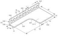
도 5를 참조하면, 발광 모듈(32)은 복수의 발광 다이오드(34) 중에서, 상기 방열부(32B)의 제1측면(S1)에 가장 가까운 발광 다이오드를 제1발광 다이오드(34A)로 정의하고, 상기 방열부(32B)의 제1측면(S1)의 반대측 제2측면(S2)에 가장 가까운 발광 다이오드를 제2발광 다이오드(34B)로 정의하고, 상기 제1 및 제2발광 다이오드(34A,34B) 사이의 영역 중심부에 배치된 발광 다이오드(들)을 제3발광 다이오드(34C)로 정의할 수 있다. 여기서, 상기 제1발광 다이오드(34A)의 위치가 다운 방향이며, 상기 제2발광 다이오드(34B)의 위치가 업 방향이 된다. 또한 상기 발광 다이오드(34) 간의 간격(T1)은 동일하거나 부분적으로 다른 간격을 가질 수 있으며, 이에 대해 한정하지는 않는다. 상기 복수의 발광 다이오드(34)는 중심이 같은 선상으로 배치될 수 있다.5, the
상기 방열부(32B)의 제2측면(S2)의 너비(D2)는 상기 기판부(32A)와 제3측면(S3) 사이의 최대 간격으로서, 제1측면(S1)의 너비(D1)보다 더 넓은 너비로 형성될 수 있다.The width D2 of the second side surface S2 of the
상기 제3측면(S3)은 상기 방열부(32B)의 제1측면(S1)과 제2측면(S2) 사이의 면으로서, 상기 제1측면(S1) 또는/및 상기 제2측면(S2)에 대해 경사진 면으로 형성될 수 있다. 상기 제3측면(S3)은 연속적인 면으로 형성될 수 있다.The third side surface S3 is a surface between the first side surface S1 and the second side surface S2 of the
상기 방열부(32B)의 상면(131-1)은 상기 제1발광 다이오드(34A)와 제3측면(S3) 사이의 간격이 가장 좁고, 제2발광 다이오드(34B)와 상기 제3측면(S3) 사이의 간격이 상기 제1발광 다이오드(34A)와 제3측면(S3) 사이의 간격보다 넓고, 상면(131-1) 영역 내에서 가장 넓게 형성될 수 있다.The upper surface 131-1 of the
이와 같이, 방열부(32B)의 상면(131-1)의 면적을 제2발광 다이오드(34B)로 갈수록 점차 넓게 배치함으로써, 열이 지나가는 방향에 배치된 상기 제1발광 다이오드(34A)보다는 제2 및 제3발광 다이오드(34B,34C)에 열이 집중될 수 있어, 방열부(32B)의 상이한 면적에 의해 방열부(32B) 내에서 균일한 열 분포를 가지도록 할 수 있다.
As described above, by arranging the area of the upper surface 131-1 of the
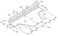
도 6는 제2실시 예에 따른 발광 모듈을 나타낸 사시도이다.6 is a perspective view illustrating a light emitting module according to a second embodiment.
도 6을 참조하면, 발광 모듈(32)은 방열부(32B)의 상면(131-2)의 센터를 중심으로 하부 영역(A1)과 상부 영역(A2)으로 구분할 수 있다. 상기 하부 영역(A1)은 제1너비(D1)로 형성되고, 상기 상부 영역(A2)는 제2너비(D2)로 형성될 수 있다.Referring to FIG. 6, the
상기 방열부(32B)의 측면(S3)은 상기 제1측면(S1) 및 제2측면(S2)으로부터 상기 제1측면(S1) 및 제2측면(S2)에 대해 직각으로 배치된 제1면(S32)과, 상기 제1면(S32) 사이에 상기 제2측면(S2)에 평행하게 대응되는 제2면(S34)를 포함한다. 상기 제1면(S32)과 상기 제2면(S34) 사이의 부분은 곡면이거나 직각으로 절곡될 수 있으나 이에 한정하지 않는다.The side surface S3 of the
상기 방열부(32B)의 제2영역(A2)은 제2 및 제3발광 다이오드(34B,34C) 사이의 영역이며, 상기 제2 및 제3발광 다이오드(34B,34C)와 상기 방열부(32B)의 제3측면(S3) 사이의 간격으로서, 제2측면(S2)의 너비(D2)로 형성될 수 있다.The second region A2 of the
상기 방열부(32B)의 제1영역(A1)은 제1 및 제2발광 다이오드(34A,34C) 사이의 영역이며, 상기 제1 및 제2발광 다이오드(34A,34C)와 상기 방열부(32B)의 제3측면(S3) 사이의 간격으로서, 제1측면(S1)의 너비(D1)로 형성될 수 있다.The first region A1 of the
상기와 같은 구조는 복수의 발광 다이오드(34)로부터 발생된 열이 표시 장치의 센터 중심부부터 더 집중될 때, 효과적으로 방열을 수행할 수 있다.
Such a structure can effectively dissipate heat when the heat generated from the plurality of
도 7은 제3실시 예에 따른 발광 모듈을 나타낸 사시도이다.7 is a perspective view illustrating a light emitting module according to a third embodiment.
도 7을 참조하면, 발광 모듈(32)의 방열부(32B)는 상면(131-3) 면적 및 너비가 영역(A11-A14)에 따라 업(UP) 방향으로 갈수록 계단 형태로 점차 증가된 구조로 형성된다. 또한 상기 각 영역(A11-A14)들의 제3측면(S3)은 제1측면(S1) 방향에서 제2측면(S2) 방향으로 갈수록 점차 넓어지는 경사진 면으로 형성되며, 상기 영역(A11~A14) 사이의 제3측면(S3)을 연결해 주는 제3면(S34)은 상기 제2측면(S2)과 대향되며 상기 제2측면(S2)과 평행하게 배치될 수 있다.7, the
또한 상기 방열부(32B)의 상면(131-3) 면적은 각 영역(A11,A14,A12,A13)에 따라 다른 너비(D1,D2,D3,D3)로 형성될 수 있다. 이러한 발광 모듈은 영역(A11~A14)에 따라 방열부(32B)의 면적으로 다르게 함으로써, 각 영역(A11~A14)별 발광 다이오드(34)의 열적 안정성을 제공할 수 있다.
The upper surface 131-3 of the
도 8은 제4실시 예에 따른 발광 모듈을 나타낸 사시도이다.8 is a perspective view illustrating a light emitting module according to a fourth embodiment.
도 8을 참조하면, 발광 모듈(32)의 방열부(32B)는 제1너비(D1)를 갖는 제1영역(A21) 및 제5영역(A25)과, 상기 제1 및 제5영역(A21,A25) 사이에 제2너비(D2)를 갖는 제3영역(A23)과, 상기 제1영역(A21)과 제3영역(A23) 사이를 연결하며 경사면(S31)을 갖는 갖는 제2영역(A22)과, 상기 제3영역(A23)과 제5영역(A25) 사이를 연결하며 경사면(S33)을 갖는 제4영역(A24)을 포함한다. 여기서, 상기 제1, 제3, 제5영역(A21,A23,A25)은 적어도 2개의 발광 다이오드가 배열되는 영역일 수 있으며, 상기 제2 및 제4영역(A22,A24)은 상기 제3영역(A23)의 면적보다 작은 면적을 갖는 영역으로서, 적어도 하나의 발광 다이오드가 배열되는 영역일 수 있으나, 이에 대해 한정하지는 않는다.8, the
상기 발광 모듈(32)의 방열부(32B)의 상면(131-4)은 센터 영역인 제3영역(A23)의 면적 및 너비를 다른 영역에 비해 더 넓게 배치하고, 각 영역(A21,A22,A23,A24,A25)에 배치된 복수의 발광 다이오드(34)로부터 발생된 열이 다른 영역 예컨대, 업(UP) 방향의 발광 다이오드들에 영향을 미치는 것을 차단할 수 있다.The upper surface 131-4 of the
여기서, 상기 발광 모듈(32)의 센터측에 배치된 제3발광 다이오드(34C)와 방열부(32B)의 제3측면(S3) 사이의 간격이 상기 센터측 보다 다운 방향 및 업 방향에 배치된 제1 및 제2발광 다이오드(34A,34B)와 방열부(32B)의 제3측면(S3) 사이의 간격보다 더 넓게 배치될 수 있다.상기 발광 모듈(32)은 업 방향의 반대측 방향에서 업 방향으로 올라오는 열을 발광 모듈(32)의 센터 영역인 제3영역(A23)과 그 주변 영역인 제2 및 제4영역(A22,A24)의 방열부(32B)에 의해 방열됨으로써, 제5영역(A25)에 배치된 발광 다이오드(34B)는 제3영역(A23)의 아래로부터 전달되는 열에 의한 간섭을 받지 않고 동작할 수 있다.
The gap between the third
도 9는 실시 예에 따른 발광 다이오드를 나타낸 측 단면도이다.9 is a side sectional view showing a light emitting diode according to an embodiment.
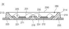
도 9를 참조하면, 발광 다이오드(34)는 제1캐비티(260)를 갖는 몸체(210), 제2캐비티(225)를 갖는 제1리드 프레임(221), 제3 캐비티(235)를 갖는 제2리드 프레임(231), 발광 칩들(271,72), 및 와이어들(201)을 포함한다.9, the
몸체(210)는 폴리프탈아미드(PPA:Polyphthalamide)와 같은 수지 재질, 실리콘(Si), 금속 재질, PSG(photo sensitive glass), 사파이어(Al2O3), 인쇄회로기판(PCB) 중 적어도 하나로 형성될 수 있다. 바람직하게 몸체(210)는 폴리프탈아미드(PPA:Polyphthalamide)와 같은 플라스틱 수지 재질로 이루어질 수 있다.
몸체(210)의 상면 형상은 발광 다이오드(34)의 용도 및 설계에 따라 삼각형, 사각형, 다각형, 및 원형 등 다양한 형상을 가질 수 있다. 상기 제1리드 프레임(221) 및 제2리드 프레임(231)은 몸체(210)의 바닥에 배치되어 직하 타입으로 기판 상에 탑재될 수 있으며, 상기 몸체(210)의 측면에 배치되어 에지 타입으로 기판 상에 탑재될 수 있으며, 이에 대해 한정하지는 않는다.The shape of the top surface of the
몸체(210)는 상부가 개방되고, 측면과 바닥으로 이루어진 제1캐비티(cavity)(260)를 갖는다. 상기 제1캐비티(260)은 상기 몸체(210)의 상면(215)으로부터 오목한 컵 구조 또는 리세스 구조를 포함할 수 있으며, 이에 대해 한정하지는 않는다. 제1캐비티(260)의 측면은 바닥에 대해 수직하거나 경사질 수 있다.The
제1캐비티(260)를 위에서 바라본 형상은 원형, 타원형, 다각형(예컨대, 사각형)일 수 있다. 제1캐비티(260)의 모서리는 곡면이거나, 평면일 수 있다.The top view of the
상기 제1리드 프레임(221)은 상기 제1캐비티(260)의 제1영역에 배치되며, 상기 제1캐비티(260)의 바닥에 일부가 배치되고 그 중심부에 상기 제1캐비티(260)의 바닥보다 더 낮은 깊이를 갖도록 오목한 제2캐비티(225)가 배치된다. 상기 제2캐비티(225)는 상기 제1리드 프레임(221)의 상면으로부터 상기 몸체(210)의 하면 방향으로 오목한 형상, 예컨대, 컵(Cup) 구조 또는 리세스(recess) 형상을 포함한다. 상기 제2캐비티(225)의 측면은 상기 제2캐비티(225)의 바닥으로부터 경사지거나 수직하게 절곡될 수 있다. 상기 제2캐비티(225)의 측면 중에서 대향되는 두 측면은 동일한 각도로 경사지거나 서로 다른 각도로 경사질 수 있다.The
상기 제2리드 프레임(231)은 상기 제1캐비티(260)의 제1영역과 이격되는 제2영역에 배치되며, 상기 제1캐비티(260)의 바닥에 일부가 배치되고, 그 중심부에는 상기 제1캐비티(260)의 바닥보다 더 낮은 깊이를 갖도록 오목한 제3캐비티(235)가 형성된다. 상기 제3캐비티(235)는 상기 제2리드 프레임(231)의 상면으로부터 상기 몸체(210)의 하면 방향으로 오목한 형상, 예컨대, 컵(Cup) 구조 또는 리세스(recess) 형상을 포함한다. 상기 제3캐비티(235)의 측면은 상기 제3캐비티(235)의 바닥으로부터 경사지거나 수직하게 절곡될 수 있다. 상기 제3캐비티(235)의 측면 중에서 대향되는 두 측면은 동일한 각도로 경사지거나 서로 다른 각도로 경사질 수 있다.The
상기 제1리드 프레임(221)의 하면 및 상기 제2리드 프레임(231)의 하면은 상기 몸체(210)의 하면으로 노출되거나, 상기 몸체(210)의 하면과 동일 평면 상에 배치될 수 있다.The lower surface of the
상기 제1리드 프레임(221)의 제1리드부(223)는 상기 몸체(210)의 하면에 배치되고 상기 몸체(210)의 제1측면(213)으로 돌출될 수 있다. 상기 제2리드 프레임(231)의 제2리드부(233)는 상기 몸체(210)의 하면에 배치되고 상기 몸체(210)의 제1측면의 반대측 제2측면(214)으로 돌출될 수 있다.The
상기 제1리드 프레임(221) 및 제2리드 프레임(231)은 금속 재질, 예를 들어, 티타늄(Ti), 구리(Cu), 니켈(Ni), 금(Au), 크롬(Cr), 탄탈늄(Ta), 백금(Pt), 주석(Sn), 은(Ag), 인(P) 중 적어도 하나를 포함할 수 있으며, 단일 금속층 또는 다층 금속층으로 형성될 수 있다. 상기 제1, 제2리드 프레임(221,231)의 두께는 동일한 두께로 형성될 수 있으며, 이에 대해 한정하지는 않는다.The
상기 제2캐비티(225) 및 상기 제3캐비티(235)의 바닥 형상은 직사각형, 정 사각형 또는 곡면을 갖는 원 또는 타원 형상일 수 있다.The bottom shapes of the
상기 몸체(210) 내에는 상기 제1 및 제2리드 프레임(221,231)를 제외한 다른 금속 프레임이 더 배치되어, 방열 프레임이나 중간 연결 단자로 사용된다.Other metal frames other than the first and second lead frames 221 and 231 are further disposed in the
상기 제1리드 프레임(221)의 제2캐비티(225) 내에는 제1발광 칩(271)이 배치되며, 상기 제2리드 프레임(231)의 제3캐비티(235) 내에는 제2발광 칩(272)이 배치될 수 있다. 상기 발광 칩(271,272)는 가시광선 대역부터 자외선 대역의 범위 중에서 선택적으로 발광할 수 있으며, 예컨대 레드 LED 칩, 블루 LED 칩, 그린 LED 칩, 엘로우 그린(yellow green) LED 칩 중에서 선택될 수 있다. 상기 발광 칩(271,72)은 III족 내지 V족 원소의 화합물 반도체 발광소자를 포함한다.The first
상기 몸체(210)의 제1캐비티(260), 상기 제2캐비티(225) 및 제3캐비티(235) 중 적어도 한 영역에는 몰딩 부재(290)가 배치되며, 상기 몰딩 부재(290)는 실리콘 또는 에폭시와 같은 투광성 수지층을 포함하며, 단층 또는 다층으로 형성될 수 있다. 상기 몰딩 부재(290) 또는 상기 발광 칩(271,272) 상에는 방출되는 빛의 파장을 변화하기 위한 형광체를 포함할 수 있으며, 상기 형광체는 발광 칩(271,272)에서 방출되는 빛의 일부를 여기시켜 다른 파장의 빛으로 방출하게 된다. 상기 형광체는 YAG, TAG, Silicate, Nitride, Oxy-nitride 계 물질 중에서 선택적으로 형성될 수 있다. 상기 형광체는 적색 형광체, 황색 형광체, 녹색 형광체 중 적어도 하나를 포함할 수 있으며, 이에 대해 한정하지는 않는다. 상기 몰딩 부재(290)의 표면은 플랫한 형상, 오목한 형상, 볼록한 형상 등으로 형성될 수 있으며, 이에 대해 한정하지는 않는다.A
상기 몸체(210)의 상부에는 렌즈가 더 형성될 수 있으며, 상기 렌즈는 오목 또는/및 볼록 렌즈의 구조를 포함할 수 있으며, 발광 다이오드(34)가 방출하는 빛의 배광(light distribution)을 조절할 수 있다.
A lens may be further formed on the
상기 제1발광 칩(272)은 상기 제1캐비티(260)의 바닥에 배치된 제1리드 프레임(221)과 제2리드 프레임(231)에 연결될 수 있으며, 그 연결 방식은 와이어(201)를 이용하거나, 다이 본딩 또는 플립 본딩 방식을 이용할 수 있다. 상기 제2발광 칩(272)은 상기 제1캐비티(260)의 바닥에 배치된 제1리드 프레임(221)과 제2리드 프레임(231)에 전기적으로 연결될 수 있으며, 그 연결 방식은 와이어(201)를 이용하거나, 다이 본딩 또는 플립 본딩 방식을 이용할 수 있다.The first
상기 제1캐비티(260) 내에는 보호 소자가 배치될 수 있으며 상기 보호소자는 싸이리스터, 제너 다이오드, 또는 TVS(Transient voltage suppression)로 구현될 수 있으며, 상기 제너 다이오드는 상기 발광 칩을 ESD(electro static discharge)로 부터 보호하게 된다.A protection element may be disposed in the
실시 예에 따른 발광 모듈은 휴대 단말기, 컴퓨터 등의 백라이트 유닛 뿐만 아니라, 조명등, 신호등, 차량 전조등, 전광판, 가로등 등의 조명 장치에 적용될 수 있으며, 이에 대해 한정하지는 않는다. 또한 직하 타입의 발광 모듈에는 상기 도광판을 배치하지 않을 수 있으며, 이에 대해 한정하지는 않는다. 또한 상기 발광 모듈 위에 렌즈 또는 유리와 같은 투광성 물질이 배치될 수 있으며, 이에 대해 한정하지는 않는다.The light emitting module according to the embodiment can be applied not only to a backlight unit such as a portable terminal and a computer, but also to an illumination device such as an illumination light, a traffic light, a vehicle headlight, an electric signboard, a streetlight, and the like. Further, the light guide plate may not be disposed in the direct-type light emitting module, but the present invention is not limited thereto. Further, a light transmitting material such as a lens or glass may be disposed on the light emitting module, but the present invention is not limited thereto.
상술한 실시 예 및 첨부된 도면에 의해 한정되는 것이 아니며, 첨부된 청구범위에 의해 한정된다. 따라서, 청구범위에 기재된 본 발명의 기술적 사상을 벗어나지 않는 범위 내에서 다양한 형태의 치환, 변형 및 변경이 가능하다는 것은 당 기술분야의 통상의 지식을 가진 자에게는 자명할 것이며, 이 또한 첨부된 청구범위에 기재된 기술적 사상에 속한다 할 것이다.The present invention is not limited to the above-described embodiment and the attached drawings, but is defined by the appended claims. It will be apparent to those skilled in the art that various changes in form and details may be made therein without departing from the spirit and scope of the invention as defined in the appended claims, As will be described below.
100: 표시장치, 10: 표시 패널, 20:백라이트 유닛, 60:광학 시트, 70:도광판, 45: 반사 부재, 30:발광 모듈, 32: 모듈 기판, 34: 발광 다이오드, 131: 금속층, 132: 절연층, 133: 배선층, 134: 보호층, 32A: 기판부, 32B: 방열부, 131-1,131-2,133-3, 133-4: 방열부 상면The present invention relates to a light emitting device and a method of manufacturing the same, and more particularly, to a light emitting diode (LED) And an upper surface of the heat dissipation part, wherein the upper surface of the heat dissipation part
Claims (15)
Translated fromKorean일면에 상기 복수의 발광 다이오드가 배치된 기판부 및 상기 기판부로부터 상기 제1축 방향과 직교하는 제2축 방향으로 절곡된 방열부를 포함하는 모듈 기판을 포함하며,
상기 모듈 기판의 방열부는 상기 제1축 방향의 서로 반대측 제1측면 및 제2측면과, 상기 제1측면과 상기 제2측면 사이의 제2축 방향의 제3측면을 포함하며,
상기 복수의 발광 다이오드는 상기 방열부의 제1측면에 인접한 제1발광 다이오드; 상기 제2측면에 인접한 제2발광 다이오드; 및 상기 제1발광 다이오드와 상기 제2발광 다이오드 사이의 영역 중에서 상기 방열부의 중앙부에 배치된 제3발광 다이오드를 포함하며,
상기 방열부는 상기 제1측면에서 제2축 방향의 제1너비가 상기 중앙부에서 제2축 방향의 너비보다 좁게 배치되며,
상기 방열부는 상기 기판부의 일면 방향으로 절곡되며,
상기 제2발광 다이오드와 상기 방열부의 제3측면 사이의 간격은 상기 제3발광 다이오드와 상기 방열부의 제3측면 사이의 간격보다 더 넓은 발광 모듈.A plurality of light emitting diodes arranged in a first axis direction; And
And a module substrate including a substrate portion having the plurality of light emitting diodes disposed on one surface thereof and a heat dissipating portion bent in a second axis direction perpendicular to the first axis direction from the substrate portion,
Wherein the heat dissipating portion of the module substrate includes a first side surface and a second side opposite to each other in the first axis direction and a third side surface in a second axis direction between the first side surface and the second side surface,
The plurality of light emitting diodes include a first light emitting diode adjacent to a first side of the heat dissipating unit; A second light emitting diode adjacent to the second side; And a third light emitting diode disposed at a central portion of the heat dissipation unit among a region between the first light emitting diode and the second light emitting diode,
Wherein the heat dissipating unit has a first width in the second axial direction on the first side surface being narrower than a width in the second axial direction in the central portion,
The heat dissipation unit is bent in one surface direction of the substrate unit,
And the gap between the second light emitting diode and the third side of the heat dissipation unit is wider than the gap between the third light emitting diode and the third side of the heat dissipation unit.
일면에 상기 복수의 발광 다이오드가 배치된 기판부 및 상기 기판부로부터 상기 제1축 방향과 직교하는 제2축 방향으로 절곡된 방열부를 포함하는 모듈 기판을 포함하며,
상기 모듈 기판의 방열부는 상기 제1축 방향의 서로 반대측 제1측면 및 제2측면과, 상기 제1측면과 상기 제2측면 사이의 제2축 방향의 제3측면을 포함하며,
상기 복수의 발광 다이오드는 상기 방열부의 제1측면에 인접한 제1발광 다이오드; 상기 제2측면에 인접한 제2발광 다이오드; 및 상기 제1발광 다이오드와 상기 제2발광 다이오드 사이의 영역 중에서 상기 방열부의 중앙부에 배치된 제3발광 다이오드를 포함하며,
상기 방열부는 상기 제1측면에서 제2축 방향의 제1너비가 상기 중앙부에서 제2축 방향의 너비보다 좁게 배치되며,
상기 방열부는 상기 기판부의 일면 방향으로 절곡되며,
상기 제3발광 다이오드와 상기 방열부의 제3측면 사이의 간격은 상기 제2발광 다이오드와 상기 방열부의 제3측면 사이의 간격보다 넓은 발광 모듈.A plurality of light emitting diodes arranged in a first axis direction; And
And a module substrate including a substrate portion having the plurality of light emitting diodes disposed on one surface thereof and a heat dissipating portion bent in a second axis direction perpendicular to the first axis direction from the substrate portion,
Wherein the heat dissipating portion of the module substrate includes a first side surface and a second side opposite to each other in the first axis direction and a third side surface in a second axis direction between the first side surface and the second side surface,
The plurality of light emitting diodes include a first light emitting diode adjacent to a first side of the heat dissipating unit; A second light emitting diode adjacent to the second side; And a third light emitting diode disposed at a central portion of the heat dissipation unit among a region between the first light emitting diode and the second light emitting diode,
Wherein the heat dissipating unit has a first width in the second axial direction on the first side surface being narrower than a width in the second axial direction in the central portion,
The heat dissipation unit is bent in one surface direction of the substrate unit,
Wherein a distance between the third light emitting diode and the third side face of the heat dissipating unit is larger than an interval between the second light emitting diode and the third side face of the heat dissipating unit.
일면에 상기 복수의 발광 다이오드가 배치된 기판부 및 상기 기판부로부터 상기 제1축 방향과 직교하는 제2축 방향으로 절곡된 방열부를 포함하는 모듈 기판을 포함하며,
상기 모듈 기판의 방열부는 상기 제1축 방향의 서로 반대측 제1측면 및 제2측면과, 상기 제1측면과 상기 제2측면 사이의 제2축 방향의 제3측면을 포함하며,
상기 복수의 발광 다이오드는 상기 방열부의 제1측면에 인접한 제1발광 다이오드; 상기 제2측면에 인접한 제2발광 다이오드; 및 상기 제1발광 다이오드와 상기 제2발광 다이오드 사이의 영역 중에서 상기 방열부의 중앙부에 배치된 제3발광 다이오드를 포함하며,
상기 방열부는 상기 제1측면에서 제2축 방향의 제1너비가 상기 중앙부에서 제2축 방향의 너비보다 좁게 배치되며,
상기 방열부는 상기 기판부의 일면 방향으로 절곡되며,
상기 방열부의 제3측면은 상기 방열부의 제1측면에 대해 경사진 면으로 형성되는 발광 모듈.A plurality of light emitting diodes arranged in a first axis direction; And
And a module substrate including a substrate portion having the plurality of light emitting diodes disposed on one surface thereof and a heat dissipating portion bent in a second axis direction perpendicular to the first axis direction from the substrate portion,
Wherein the heat dissipating portion of the module substrate includes a first side surface and a second side opposite to each other in the first axis direction and a third side surface in a second axis direction between the first side surface and the second side surface,
The plurality of light emitting diodes include a first light emitting diode adjacent to a first side of the heat dissipating unit; A second light emitting diode adjacent to the second side; And a third light emitting diode disposed at a central portion of the heat dissipation unit among a region between the first light emitting diode and the second light emitting diode,
Wherein the heat dissipating unit has a first width in the second axial direction on the first side surface being narrower than a width in the second axial direction in the central portion,
The heat dissipation unit is bent in one surface direction of the substrate unit,
And the third side surface of the heat dissipation unit is formed as an inclined surface with respect to the first side surface of the heat dissipation unit.
일면에 상기 복수의 발광 다이오드가 배치된 기판부 및 상기 기판부로부터 상기 제1축 방향과 직교하는 제2축 방향으로 절곡된 방열부를 포함하는 모듈 기판을 포함하며,
상기 모듈 기판의 방열부는 상기 제1축 방향의 서로 반대측 제1측면 및 제2측면과, 상기 제1측면과 상기 제2측면 사이의 제2축 방향의 제3측면을 포함하며,
상기 복수의 발광 다이오드는 상기 방열부의 제1측면에 인접한 제1발광 다이오드; 상기 제2측면에 인접한 제2발광 다이오드; 및 상기 제1발광 다이오드와 상기 제2발광 다이오드 사이의 영역 중에서 상기 방열부의 중앙부에 배치된 제3발광 다이오드를 포함하며,
상기 방열부는 상기 제1측면에서 제2축 방향의 제1너비가 상기 중앙부에서 제2축 방향의 너비보다 좁게 배치되며,
상기 방열부는 상기 기판부의 일면 방향으로 절곡되며,
상기 방열부의 제3측면은 상기 방열부의 제2측면의 반대측 제4측면을 더 포함하는 발광 모듈.A plurality of light emitting diodes arranged in a first axis direction; And
And a module substrate including a substrate portion having the plurality of light emitting diodes disposed on one surface thereof and a heat dissipating portion bent in a second axis direction perpendicular to the first axis direction from the substrate portion,
Wherein the heat dissipating portion of the module substrate includes a first side surface and a second side opposite to each other in the first axis direction and a third side surface in a second axis direction between the first side surface and the second side surface,
The plurality of light emitting diodes include a first light emitting diode adjacent to a first side of the heat dissipating unit; A second light emitting diode adjacent to the second side; And a third light emitting diode disposed at a central portion of the heat dissipation unit among a region between the first light emitting diode and the second light emitting diode,
Wherein the heat dissipating unit has a first width in the second axial direction on the first side surface being narrower than a width in the second axial direction in the central portion,
The heat dissipation unit is bent in one surface direction of the substrate unit,
And the third side surface of the heat dissipation unit further includes a fourth side surface opposite to the second side surface of the heat dissipation unit.
일면에 상기 복수의 발광 다이오드가 배치된 기판부 및 상기 기판부로부터 상기 제1축 방향과 직교하는 제2축 방향으로 절곡된 방열부를 포함하는 모듈 기판을 포함하며,
상기 모듈 기판의 방열부는 상기 제1축 방향의 서로 반대측 제1측면 및 제2측면과, 상기 제1측면과 상기 제2측면 사이의 제2축 방향의 제3측면을 포함하며,
상기 복수의 발광 다이오드는 상기 방열부의 제1측면에 인접한 제1발광 다이오드; 상기 제2측면에 인접한 제2발광 다이오드; 및 상기 제1발광 다이오드와 상기 제2발광 다이오드 사이의 영역 중에서 상기 방열부의 중앙부에 배치된 제3발광 다이오드를 포함하며,
상기 방열부는 상기 제1측면에서 제2축 방향의 제1너비가 상기 중앙부에서 제2축 방향의 너비보다 좁게 배치되며,
상기 방열부는 상기 기판부의 일면 방향으로 절곡되며,
상기 방열부의 제3측면은 상기 방열부의 제1측면 또는 제2측면과 수직하게 배치된 제5측면을 포함하는 발광 모듈.A plurality of light emitting diodes arranged in a first axis direction; And
And a module substrate including a substrate portion having the plurality of light emitting diodes disposed on one surface thereof and a heat dissipating portion bent in a second axis direction perpendicular to the first axis direction from the substrate portion,
Wherein the heat dissipating portion of the module substrate includes a first side surface and a second side opposite to each other in the first axis direction and a third side surface in a second axis direction between the first side surface and the second side surface,
The plurality of light emitting diodes include a first light emitting diode adjacent to a first side of the heat dissipating unit; A second light emitting diode adjacent to the second side; And a third light emitting diode disposed at a central portion of the heat dissipation unit among a region between the first light emitting diode and the second light emitting diode,
Wherein the heat dissipating unit has a first width in the second axial direction on the first side surface being narrower than a width in the second axial direction in the central portion,
The heat dissipation unit is bent in one surface direction of the substrate unit,
And the third side surface of the heat dissipation portion includes a fifth side surface disposed perpendicularly to the first side surface or the second side surface of the heat dissipation portion.
상기 절연층은 상기 방열부로부터 이격되는 발광 모듈.7. The module board according to any one of claims 1 to 6, wherein the module substrate comprises: a metal layer; An insulating layer on the metal layer; And a wiring layer on the insulating layer,
Wherein the insulating layer is spaced apart from the heat dissipation unit.
상기 기판부의 두께는 상기 방열부의 두께보다 두꺼운 발광 모듈.[8] The apparatus of claim 7, wherein the heat dissipation unit is formed of the metal layer,
Wherein a thickness of the substrate portion is thicker than a thickness of the heat dissipation portion.
상기 바텀 커버 상에 도광판; 및
상기 바텀 커버의 제1측면부의 내측에 배치된 기판부, 및 상기 기판부로부터 절곡되어 상기 바텀 커버의 바닥부에 배치된 방열부를 포함하는 모듈 기판; 및 상기 모듈 기판의 상기 기판부 상에 배치되고 상기 도광판의 적어도 한 측면에 대응되는 복수의 발광 다이오드를 포함하는 발광 모듈을 포함하며,
상기 모듈 기판은 청구항 제1항 내지 제6항 중 어느 한 항의 모듈 기판을 포함하는 백라이트 유닛.A bottom cover including a bottom portion and a first side portion bent from the bottom portion;
A light guide plate on the bottom cover; And
A module substrate including a substrate portion disposed on an inner side of a first side portion of the bottom cover and a heat dissipation portion bent from the substrate portion and disposed on a bottom portion of the bottom cover; And a light emitting module including a plurality of light emitting diodes disposed on the substrate portion of the module substrate and corresponding to at least one side surface of the light guide plate,
Wherein the module substrate comprises the module substrate of any one of claims 1 to 6.
Priority Applications (4)
| Application Number | Priority Date | Filing Date | Title |
|---|---|---|---|
| KR1020110084799AKR101884628B1 (en) | 2011-08-24 | 2011-08-24 | Light emitting module and backlight unit having the same |
| US13/369,801US8752995B2 (en) | 2011-08-24 | 2012-02-09 | Light emitting module and backlight unit having the same |
| EP12157386.9AEP2563102B1 (en) | 2011-08-24 | 2012-02-28 | Light emitting module and backlight unit having the same |
| CN201210058723.8ACN102954398B (en) | 2011-08-24 | 2012-03-07 | Light emitting module and the back light unit with light emitting module |
Applications Claiming Priority (1)
| Application Number | Priority Date | Filing Date | Title |
|---|---|---|---|
| KR1020110084799AKR101884628B1 (en) | 2011-08-24 | 2011-08-24 | Light emitting module and backlight unit having the same |
Publications (2)
| Publication Number | Publication Date |
|---|---|
| KR20130022074A KR20130022074A (en) | 2013-03-06 |
| KR101884628B1true KR101884628B1 (en) | 2018-08-02 |
Family
ID=45930564
Family Applications (1)
| Application Number | Title | Priority Date | Filing Date |
|---|---|---|---|
| KR1020110084799AExpired - Fee RelatedKR101884628B1 (en) | 2011-08-24 | 2011-08-24 | Light emitting module and backlight unit having the same |
Country Status (4)
| Country | Link |
|---|---|
| US (1) | US8752995B2 (en) |
| EP (1) | EP2563102B1 (en) |
| KR (1) | KR101884628B1 (en) |
| CN (1) | CN102954398B (en) |
Families Citing this family (45)
| Publication number | Priority date | Publication date | Assignee | Title |
|---|---|---|---|---|
| KR100986380B1 (en) | 2009-11-20 | 2010-10-08 | 엘지이노텍 주식회사 | Light emitting apparatus |
| US20140375891A1 (en)* | 2012-02-03 | 2014-12-25 | Sharp Kabushiki Kaisha | Display device, and television receiver device |
| KR102099590B1 (en) | 2012-05-18 | 2020-04-10 | 리얼디 스파크, 엘엘씨 | Controlling light sources of a directional backlight |
| EP2850488A4 (en) | 2012-05-18 | 2016-03-02 | Reald Inc | Directional backlight |
| US9235057B2 (en) | 2012-05-18 | 2016-01-12 | Reald Inc. | Polarization recovery in a directional display device |
| US9188731B2 (en) | 2012-05-18 | 2015-11-17 | Reald Inc. | Directional backlight |
| US9678267B2 (en) | 2012-05-18 | 2017-06-13 | Reald Spark, Llc | Wide angle imaging directional backlights |
| CN111487707A (en) | 2013-02-22 | 2020-08-04 | 瑞尔D斯帕克有限责任公司 | directional backlight |
| KR102254799B1 (en) | 2013-06-17 | 2021-05-24 | 리얼디 스파크, 엘엘씨 | Controlling light sources of a directional backlight |
| WO2014208368A1 (en)* | 2013-06-27 | 2014-12-31 | 堺ディスプレイプロダクト株式会社 | Light source device and display device |
| KR102150611B1 (en)* | 2013-07-02 | 2020-09-01 | 엘지이노텍 주식회사 | Printed circuit board |
| KR102090156B1 (en)* | 2013-07-04 | 2020-03-18 | 삼성디스플레이 주식회사 | Display device |
| KR102366346B1 (en) | 2013-10-14 | 2022-02-23 | 리얼디 스파크, 엘엘씨 | Light input for directional backlight |
| EP3058562A4 (en) | 2013-10-14 | 2017-07-26 | RealD Spark, LLC | Control of directional display |
| CN106062466B (en) | 2013-11-15 | 2020-01-31 | 瑞尔D斯帕克有限责任公司 | Directional backlight with light emitting element package |
| KR102203682B1 (en)* | 2014-03-07 | 2021-01-15 | 엘지이노텍 주식회사 | Printed circuit board |
| CN103982821B (en)* | 2014-05-19 | 2017-02-15 | 京东方科技集团股份有限公司 | backlight source and display device |
| EP3161550A4 (en) | 2014-06-26 | 2018-04-18 | RealD Spark, LLC | Directional privacy display |
| USD838253S1 (en)* | 2014-07-04 | 2019-01-15 | Sakai Display Products Corporation | Image display |
| USD873822S1 (en) | 2014-07-04 | 2020-01-28 | Sakai Display Products Corporation | Image display |
| USD877147S1 (en) | 2014-07-04 | 2020-03-03 | Sakai Display Products Corporation | Image display |
| US9379298B2 (en)* | 2014-10-03 | 2016-06-28 | Henkel IP & Holding GmbH | Laminate sub-mounts for LED surface mount package |
| WO2016057690A1 (en) | 2014-10-08 | 2016-04-14 | Reald Inc. | Directional backlight |
| KR102354912B1 (en)* | 2014-11-18 | 2022-01-24 | 엘지디스플레이 주식회사 | Light source unit for backlight unit and liquid display device having the same |
| US10356383B2 (en) | 2014-12-24 | 2019-07-16 | Reald Spark, Llc | Adjustment of perceived roundness in stereoscopic image of a head |
| WO2016168345A1 (en) | 2015-04-13 | 2016-10-20 | Reald Inc. | Wide angle imaging directional backlights |
| CN107850804B (en) | 2015-05-27 | 2021-06-11 | 瑞尔D斯帕克有限责任公司 | Wide-angle imaging directional backlight |
| WO2017038663A1 (en)* | 2015-08-31 | 2017-03-09 | シャープ株式会社 | Illumination device and display device |
| JP6862141B2 (en) | 2015-10-14 | 2021-04-21 | エルジー イノテック カンパニー リミテッド | Light emitting element package and lighting equipment |
| US10475418B2 (en) | 2015-10-26 | 2019-11-12 | Reald Spark, Llc | Intelligent privacy system, apparatus, and method thereof |
| WO2017083526A1 (en) | 2015-11-10 | 2017-05-18 | Reald Inc. | Distortion matching polarization conversion systems and methods thereof |
| WO2017083583A1 (en) | 2015-11-13 | 2017-05-18 | Reald Spark, Llc | Surface features for imaging directional backlights |
| EP3374692B1 (en) | 2015-11-13 | 2021-02-24 | RealD Spark, LLC | Wide angle imaging directional backlights |
| CN114143495B (en) | 2016-01-05 | 2025-07-15 | 瑞尔D斯帕克有限责任公司 | Gaze Correction for Multi-View Images |
| CN106019717B (en)* | 2016-08-03 | 2023-07-14 | 江西联思触控技术有限公司 | Backlight module, liquid crystal display module and liquid crystal display device |
| US10317614B1 (en)* | 2017-03-14 | 2019-06-11 | Automatad Assembly Corporation | SSL lighting apparatus |
| KR102443605B1 (en)* | 2017-09-06 | 2022-09-15 | 삼성디스플레이 주식회사 | Cover window for display device and manufacturing method thereof |
| JP6949643B2 (en) | 2017-09-28 | 2021-10-13 | 株式会社ジャパンディスプレイ | Lighting device and display device |
| CN107966853A (en)* | 2017-11-17 | 2018-04-27 | 武汉华星光电技术有限公司 | Liquid crystal display and its backlight module |
| US10655823B1 (en) | 2019-02-04 | 2020-05-19 | Automated Assembly Corporation | SSL lighting apparatus |
| US10995931B1 (en) | 2020-08-06 | 2021-05-04 | Automated Assembly Corporation | SSL lighting apparatus |
| CN116194812A (en) | 2020-09-16 | 2023-05-30 | 瑞尔D斯帕克有限责任公司 | Vehicle Exterior Lighting |
| KR20220116857A (en)* | 2021-02-16 | 2022-08-23 | 삼성전자주식회사 | Glass assembly and electronic device including the same |
| US11966049B2 (en) | 2022-08-02 | 2024-04-23 | Reald Spark, Llc | Pupil tracking near-eye display |
| WO2024035796A1 (en) | 2022-08-11 | 2024-02-15 | Reald Spark, Llc | Anamorphic directional illumination device |
Citations (3)
| Publication number | Priority date | Publication date | Assignee | Title |
|---|---|---|---|---|
| JP2008186780A (en) | 2007-01-31 | 2008-08-14 | Mitsubishi Electric Corp | Light source device and planar light source device including the light source device |
| US20080304288A1 (en) | 2007-06-08 | 2008-12-11 | Fujifilm Corporation | Planar lighting device |
| JP2010097924A (en)* | 2008-09-18 | 2010-04-30 | Hitachi Ltd | Liquid crystal display unit |
Family Cites Families (12)
| Publication number | Priority date | Publication date | Assignee | Title |
|---|---|---|---|---|
| KR100772374B1 (en)* | 2005-03-12 | 2007-11-01 | 삼성전자주식회사 | Edge-lit backlight unit with heat dissipation system |
| US7553055B2 (en) | 2005-12-08 | 2009-06-30 | Tpo Displays Corp. | Systems for displaying images |
| CN100538473C (en)* | 2005-12-08 | 2009-09-09 | 统宝光电股份有限公司 | Image display system and liquid crystal display module thereof |
| TWI322915B (en) | 2006-03-31 | 2010-04-01 | Au Optronics Corp | Heat dissipation structure of backliht module |
| KR20080034717A (en)* | 2006-10-17 | 2008-04-22 | 주식회사 우영 | Edge type LED backlight unit |
| US7677782B2 (en)* | 2008-01-18 | 2010-03-16 | Arima Optoelectronics Corp. | LED flat lamp |
| TWI363234B (en)* | 2008-11-18 | 2012-05-01 | Au Optronics Corp | Backlight module and lcd panel display using the same |
| TWI391752B (en)* | 2009-03-24 | 2013-04-01 | Au Optronics Corp | Display device and backlight module with thermal isolating layer |
| KR101255833B1 (en)* | 2009-07-09 | 2013-04-16 | 엘지디스플레이 주식회사 | Liquid crystal display device |
| KR101670715B1 (en) | 2010-01-08 | 2016-11-10 | 삼성디스플레이 주식회사 | Backlight unit and liquid crystal display having the same |
| TWI431365B (en)* | 2011-03-01 | 2014-03-21 | E Ink Holdings Inc | Backlight module having light-emitting diode |
| KR101295358B1 (en)* | 2011-03-16 | 2013-08-12 | 삼성전자주식회사 | Liquid crystal display and LED module provided therein |
- 2011
- 2011-08-24KRKR1020110084799Apatent/KR101884628B1/ennot_activeExpired - Fee Related
- 2012
- 2012-02-09USUS13/369,801patent/US8752995B2/enactiveActive
- 2012-02-28EPEP12157386.9Apatent/EP2563102B1/enactiveActive
- 2012-03-07CNCN201210058723.8Apatent/CN102954398B/enactiveActive
Patent Citations (3)
| Publication number | Priority date | Publication date | Assignee | Title |
|---|---|---|---|---|
| JP2008186780A (en) | 2007-01-31 | 2008-08-14 | Mitsubishi Electric Corp | Light source device and planar light source device including the light source device |
| US20080304288A1 (en) | 2007-06-08 | 2008-12-11 | Fujifilm Corporation | Planar lighting device |
| JP2010097924A (en)* | 2008-09-18 | 2010-04-30 | Hitachi Ltd | Liquid crystal display unit |
Also Published As
| Publication number | Publication date |
|---|---|
| KR20130022074A (en) | 2013-03-06 |
| EP2563102A1 (en) | 2013-02-27 |
| CN102954398A (en) | 2013-03-06 |
| US20130051073A1 (en) | 2013-02-28 |
| CN102954398B (en) | 2016-08-10 |
| US8752995B2 (en) | 2014-06-17 |
| EP2563102B1 (en) | 2018-12-05 |
Similar Documents
| Publication | Publication Date | Title |
|---|---|---|
| KR101884628B1 (en) | Light emitting module and backlight unit having the same | |
| KR101886127B1 (en) | Light emitting module and backlight unit having the same | |
| US8864357B2 (en) | Light emitting device and light unit having the same | |
| EP2587561B1 (en) | Light source module | |
| US20110215349A1 (en) | Light emitting device and light unit having the same | |
| EP2354819B1 (en) | Backlight unit and display device using the same | |
| US8853726B2 (en) | Light emitting device package and lighting system having the same | |
| KR101655505B1 (en) | Light emitting device | |
| KR101641744B1 (en) | Light emitting device package and backlight unit having the same | |
| KR101873586B1 (en) | Display device | |
| KR101750954B1 (en) | Light emitting device package and backlight unit having the same | |
| KR101892921B1 (en) | Light emitting module and backlight unit having the same | |
| KR101786071B1 (en) | Backlight unit and display appratus having the same | |
| KR101856218B1 (en) | Light emitting module and backlight unit having the same | |
| KR101880058B1 (en) | Light emitting device package and lighting apparatus having the same | |
| KR101852810B1 (en) | Fixing apparatus of connector | |
| KR101210202B1 (en) | Light emitting module and backlight unit having the same | |
| KR100821222B1 (en) | Rod-shaped LED Package and Manufacturing Method Thereof | |
| KR101946834B1 (en) | Light emitting device packae and light unit having the same | |
| KR101896692B1 (en) | Light emitting device | |
| KR101926468B1 (en) | Light emitting device package | |
| KR101894933B1 (en) | Light Emitting Device Package | |
| KR20140145402A (en) | Light unit | |
| KR20140011155A (en) | Light emitting device | |
| KR20130068496A (en) | Light emitting module |
Legal Events
| Date | Code | Title | Description |
|---|---|---|---|
| PA0109 | Patent application | St.27 status event code:A-0-1-A10-A12-nap-PA0109 | |
| PG1501 | Laying open of application | St.27 status event code:A-1-1-Q10-Q12-nap-PG1501 | |
| PN2301 | Change of applicant | St.27 status event code:A-3-3-R10-R13-asn-PN2301 St.27 status event code:A-3-3-R10-R11-asn-PN2301 | |
| R17-X000 | Change to representative recorded | St.27 status event code:A-3-3-R10-R17-oth-X000 | |
| A201 | Request for examination | ||
| P11-X000 | Amendment of application requested | St.27 status event code:A-2-2-P10-P11-nap-X000 | |
| P13-X000 | Application amended | St.27 status event code:A-2-2-P10-P13-nap-X000 | |
| PA0201 | Request for examination | St.27 status event code:A-1-2-D10-D11-exm-PA0201 | |
| R18-X000 | Changes to party contact information recorded | St.27 status event code:A-3-3-R10-R18-oth-X000 | |
| E902 | Notification of reason for refusal | ||
| PE0902 | Notice of grounds for rejection | St.27 status event code:A-1-2-D10-D21-exm-PE0902 | |
| P11-X000 | Amendment of application requested | St.27 status event code:A-2-2-P10-P11-nap-X000 | |
| P13-X000 | Application amended | St.27 status event code:A-2-2-P10-P13-nap-X000 | |
| R17-X000 | Change to representative recorded | St.27 status event code:A-3-3-R10-R17-oth-X000 | |
| E701 | Decision to grant or registration of patent right | ||
| PE0701 | Decision of registration | St.27 status event code:A-1-2-D10-D22-exm-PE0701 | |
| R18-X000 | Changes to party contact information recorded | St.27 status event code:A-3-3-R10-R18-oth-X000 | |
| PR0701 | Registration of establishment | St.27 status event code:A-2-4-F10-F11-exm-PR0701 | |
| PR1002 | Payment of registration fee | St.27 status event code:A-2-2-U10-U11-oth-PR1002 Fee payment year number:1 | |
| PG1601 | Publication of registration | St.27 status event code:A-4-4-Q10-Q13-nap-PG1601 | |
| P22-X000 | Classification modified | St.27 status event code:A-4-4-P10-P22-nap-X000 | |
| R18-X000 | Changes to party contact information recorded | St.27 status event code:A-5-5-R10-R18-oth-X000 | |
| PN2301 | Change of applicant | St.27 status event code:A-5-5-R10-R13-asn-PN2301 St.27 status event code:A-5-5-R10-R11-asn-PN2301 | |
| PR1001 | Payment of annual fee | St.27 status event code:A-4-4-U10-U11-oth-PR1001 Fee payment year number:4 | |
| PN2301 | Change of applicant | St.27 status event code:A-5-5-R10-R11-asn-PN2301 | |
| PN2301 | Change of applicant | St.27 status event code:A-5-5-R10-R14-asn-PN2301 | |
| PR1001 | Payment of annual fee | St.27 status event code:A-4-4-U10-U11-oth-PR1001 Fee payment year number:5 | |
| PC1903 | Unpaid annual fee | St.27 status event code:A-4-4-U10-U13-oth-PC1903 Not in force date:20230728 Payment event data comment text:Termination Category : DEFAULT_OF_REGISTRATION_FEE | |
| PC1903 | Unpaid annual fee | St.27 status event code:N-4-6-H10-H13-oth-PC1903 Ip right cessation event data comment text:Termination Category : DEFAULT_OF_REGISTRATION_FEE Not in force date:20230728 |