KR101881133B1 - Method of forming an inclided structure in an insulation layer, organic light emitting device and method of manufcaturing an organic light emitting device - Google Patents
Method of forming an inclided structure in an insulation layer, organic light emitting device and method of manufcaturing an organic light emitting deviceDownload PDFInfo
- Publication number
- KR101881133B1 KR101881133B1KR1020120059068AKR20120059068AKR101881133B1KR 101881133 B1KR101881133 B1KR 101881133B1KR 1020120059068 AKR1020120059068 AKR 1020120059068AKR 20120059068 AKR20120059068 AKR 20120059068AKR 101881133 B1KR101881133 B1KR 101881133B1
- Authority
- KR
- South Korea
- Prior art keywords
- light emitting
- electrode
- organic light
- layer
- insulating layer
- Prior art date
- Legal status (The legal status is an assumption and is not a legal conclusion. Google has not performed a legal analysis and makes no representation as to the accuracy of the status listed.)
- Active
Links
- 238000000034methodMethods0.000titledescription168
- 238000009413insulationMethods0.000title1
- 239000000758substrateSubstances0.000claimsabstractdescription82
- 239000010410layerSubstances0.000description302
- 239000010408filmSubstances0.000description194
- 239000004065semiconductorSubstances0.000description39
- 230000001681protective effectEffects0.000description33
- 239000000463materialSubstances0.000description29
- XUIMIQQOPSSXEZ-UHFFFAOYSA-NSiliconChemical compound[Si]XUIMIQQOPSSXEZ-UHFFFAOYSA-N0.000description26
- 229910052710siliconInorganic materials0.000description26
- 239000010703siliconSubstances0.000description26
- XLOMVQKBTHCTTD-UHFFFAOYSA-NZinc monoxideChemical compound[Zn]=OXLOMVQKBTHCTTD-UHFFFAOYSA-N0.000description25
- 238000005229chemical vapour depositionMethods0.000description22
- 238000004519manufacturing processMethods0.000description20
- 229920000642polymerPolymers0.000description20
- 239000011229interlayerSubstances0.000description19
- 229910052751metalInorganic materials0.000description18
- 239000002184metalSubstances0.000description18
- 239000011241protective layerSubstances0.000description18
- GWEVSGVZZGPLCZ-UHFFFAOYSA-NTitan oxideChemical compoundO=[Ti]=OGWEVSGVZZGPLCZ-UHFFFAOYSA-N0.000description16
- OGIDPMRJRNCKJF-UHFFFAOYSA-Ntitanium oxideInorganic materials[Ti]=OOGIDPMRJRNCKJF-UHFFFAOYSA-N0.000description16
- 239000000956alloySubstances0.000description14
- 229910045601alloyInorganic materials0.000description14
- 239000011368organic materialSubstances0.000description13
- 238000007639printingMethods0.000description13
- 229920005989resinPolymers0.000description13
- 239000011347resinSubstances0.000description13
- 238000004544sputter depositionMethods0.000description13
- 239000011787zinc oxideSubstances0.000description13
- 238000011049fillingMethods0.000description12
- 229910010272inorganic materialInorganic materials0.000description12
- 239000011147inorganic materialSubstances0.000description12
- 238000000623plasma-assisted chemical vapour depositionMethods0.000description12
- 238000000231atomic layer depositionMethods0.000description11
- 238000002161passivationMethods0.000description11
- 238000005530etchingMethods0.000description10
- 239000010936titaniumSubstances0.000description10
- 238000001771vacuum depositionMethods0.000description10
- 229910052581Si3N4Inorganic materials0.000description9
- 229910052782aluminiumInorganic materials0.000description9
- XAGFODPZIPBFFR-UHFFFAOYSA-NaluminiumChemical compound[Al]XAGFODPZIPBFFR-UHFFFAOYSA-N0.000description9
- 239000004020conductorSubstances0.000description9
- 229910000449hafnium oxideInorganic materials0.000description9
- 229910044991metal oxideInorganic materials0.000description9
- 150000004706metal oxidesChemical class0.000description9
- IJGRMHOSHXDMSA-UHFFFAOYSA-NAtomic nitrogenChemical compoundN#NIJGRMHOSHXDMSA-UHFFFAOYSA-N0.000description8
- VYPSYNLAJGMNEJ-UHFFFAOYSA-NSilicium dioxideChemical compoundO=[Si]=OVYPSYNLAJGMNEJ-UHFFFAOYSA-N0.000description8
- RTAQQCXQSZGOHL-UHFFFAOYSA-NTitaniumChemical compound[Ti]RTAQQCXQSZGOHL-UHFFFAOYSA-N0.000description8
- TWNQGVIAIRXVLR-UHFFFAOYSA-Noxo(oxoalumanyloxy)alumaneChemical compoundO=[Al]O[Al]=OTWNQGVIAIRXVLR-UHFFFAOYSA-N0.000description8
- BPUBBGLMJRNUCC-UHFFFAOYSA-Noxygen(2-);tantalum(5+)Chemical compound[O-2].[O-2].[O-2].[O-2].[O-2].[Ta+5].[Ta+5]BPUBBGLMJRNUCC-UHFFFAOYSA-N0.000description8
- RVTZCBVAJQQJTK-UHFFFAOYSA-Noxygen(2-);zirconium(4+)Chemical compound[O-2].[O-2].[Zr+4]RVTZCBVAJQQJTK-UHFFFAOYSA-N0.000description8
- 238000004528spin coatingMethods0.000description8
- 229910001936tantalum oxideInorganic materials0.000description8
- 229910052719titaniumInorganic materials0.000description8
- 229910001928zirconium oxideInorganic materials0.000description8
- AJNVQOSZGJRYEI-UHFFFAOYSA-Ndigallium;oxygen(2-)Chemical compound[O-2].[O-2].[O-2].[Ga+3].[Ga+3]AJNVQOSZGJRYEI-UHFFFAOYSA-N0.000description7
- 229910001195gallium oxideInorganic materials0.000description7
- BASFCYQUMIYNBI-UHFFFAOYSA-NplatinumChemical compound[Pt]BASFCYQUMIYNBI-UHFFFAOYSA-N0.000description7
- 229920001721polyimidePolymers0.000description7
- 150000003377silicon compoundsChemical class0.000description7
- 229910052814silicon oxideInorganic materials0.000description7
- 229910052715tantalumInorganic materials0.000description7
- GUVRBAGPIYLISA-UHFFFAOYSA-Ntantalum atomChemical compound[Ta]GUVRBAGPIYLISA-UHFFFAOYSA-N0.000description7
- 239000000470constituentSubstances0.000description6
- WIHZLLGSGQNAGK-UHFFFAOYSA-Nhafnium(4+);oxygen(2-)Chemical compound[O-2].[O-2].[Hf+4]WIHZLLGSGQNAGK-UHFFFAOYSA-N0.000description6
- CPLXHLVBOLITMK-UHFFFAOYSA-Nmagnesium oxideInorganic materials[Mg]=OCPLXHLVBOLITMK-UHFFFAOYSA-N0.000description6
- 229920002120photoresistant polymerPolymers0.000description6
- HQVNEWCFYHHQES-UHFFFAOYSA-Nsilicon nitrideChemical compoundN12[Si]34N5[Si]62N3[Si]51N64HQVNEWCFYHHQES-UHFFFAOYSA-N0.000description6
- 239000002356single layerSubstances0.000description6
- BQCADISMDOOEFD-UHFFFAOYSA-NSilverChemical compound[Ag]BQCADISMDOOEFD-UHFFFAOYSA-N0.000description5
- -1acrylChemical group0.000description5
- KPUWHANPEXNPJT-UHFFFAOYSA-NdisiloxaneChemical class[SiH3]O[SiH3]KPUWHANPEXNPJT-UHFFFAOYSA-N0.000description5
- 229910052735hafniumInorganic materials0.000description5
- VBJZVLUMGGDVMO-UHFFFAOYSA-Nhafnium atomChemical compound[Hf]VBJZVLUMGGDVMO-UHFFFAOYSA-N0.000description5
- 239000012535impuritySubstances0.000description5
- 229910003437indium oxideInorganic materials0.000description5
- PJXISJQVUVHSOJ-UHFFFAOYSA-Nindium(iii) oxideChemical compound[O-2].[O-2].[O-2].[In+3].[In+3]PJXISJQVUVHSOJ-UHFFFAOYSA-N0.000description5
- 239000000395magnesium oxideSubstances0.000description5
- 150000004767nitridesChemical class0.000description5
- 229920003986novolacPolymers0.000description5
- 230000003287optical effectEffects0.000description5
- 239000012044organic layerSubstances0.000description5
- 229920002647polyamidePolymers0.000description5
- 229910052709silverInorganic materials0.000description5
- 239000004332silverSubstances0.000description5
- 229910052721tungstenInorganic materials0.000description5
- 239000010937tungstenSubstances0.000description5
- 239000004925Acrylic resinSubstances0.000description4
- FYYHWMGAXLPEAU-UHFFFAOYSA-NMagnesiumChemical compound[Mg]FYYHWMGAXLPEAU-UHFFFAOYSA-N0.000description4
- 239000004952PolyamideSubstances0.000description4
- 239000004642PolyimideSubstances0.000description4
- HCHKCACWOHOZIP-UHFFFAOYSA-NZincChemical compound[Zn]HCHKCACWOHOZIP-UHFFFAOYSA-N0.000description4
- QCWXUUIWCKQGHC-UHFFFAOYSA-NZirconiumChemical compound[Zr]QCWXUUIWCKQGHC-UHFFFAOYSA-N0.000description4
- NIXOWILDQLNWCW-UHFFFAOYSA-Nacrylic acid groupChemical groupC(C=C)(=O)ONIXOWILDQLNWCW-UHFFFAOYSA-N0.000description4
- 125000003178carboxy groupChemical group[H]OC(*)=O0.000description4
- 239000010949copperSubstances0.000description4
- AMGQUBHHOARCQH-UHFFFAOYSA-Nindium;oxotinChemical compound[In].[Sn]=OAMGQUBHHOARCQH-UHFFFAOYSA-N0.000description4
- 239000011261inert gasSubstances0.000description4
- 229910052749magnesiumInorganic materials0.000description4
- 239000011777magnesiumSubstances0.000description4
- AXZKOIWUVFPNLO-UHFFFAOYSA-Nmagnesium;oxygen(2-)Chemical compound[O-2].[Mg+2]AXZKOIWUVFPNLO-UHFFFAOYSA-N0.000description4
- 229910052757nitrogenInorganic materials0.000description4
- 229920000058polyacrylatePolymers0.000description4
- 229910001887tin oxideInorganic materials0.000description4
- 238000002834transmittanceMethods0.000description4
- 229910052725zincInorganic materials0.000description4
- 239000011701zincSubstances0.000description4
- YVTHLONGBIQYBO-UHFFFAOYSA-Nzinc indium(3+) oxygen(2-)Chemical compound[O--].[Zn++].[In+3]YVTHLONGBIQYBO-UHFFFAOYSA-N0.000description4
- 229910052726zirconiumInorganic materials0.000description4
- RYGMFSIKBFXOCR-UHFFFAOYSA-NCopperChemical compound[Cu]RYGMFSIKBFXOCR-UHFFFAOYSA-N0.000description3
- ZOKXTWBITQBERF-UHFFFAOYSA-NMolybdenumChemical compound[Mo]ZOKXTWBITQBERF-UHFFFAOYSA-N0.000description3
- KDLHZDBZIXYQEI-UHFFFAOYSA-NPalladiumChemical compound[Pd]KDLHZDBZIXYQEI-UHFFFAOYSA-N0.000description3
- 239000011651chromiumSubstances0.000description3
- 229910052802copperInorganic materials0.000description3
- 230000014509gene expressionEffects0.000description3
- 239000011521glassSubstances0.000description3
- 229910052750molybdenumInorganic materials0.000description3
- 239000011733molybdenumSubstances0.000description3
- 229910052697platinumInorganic materials0.000description3
- 238000004549pulsed laser depositionMethods0.000description3
- 239000000126substanceSubstances0.000description3
- 239000010409thin filmSubstances0.000description3
- XOLBLPGZBRYERU-UHFFFAOYSA-Ntin dioxideChemical compoundO=[Sn]=OXOLBLPGZBRYERU-UHFFFAOYSA-N0.000description3
- WFKWXMTUELFFGS-UHFFFAOYSA-NtungstenChemical compound[W]WFKWXMTUELFFGS-UHFFFAOYSA-N0.000description3
- 229920000178Acrylic resinPolymers0.000description2
- VYZAMTAEIAYCRO-UHFFFAOYSA-NChromiumChemical compound[Cr]VYZAMTAEIAYCRO-UHFFFAOYSA-N0.000description2
- 229910052779NeodymiumInorganic materials0.000description2
- PXHVJJICTQNCMI-UHFFFAOYSA-NNickelChemical compound[Ni]PXHVJJICTQNCMI-UHFFFAOYSA-N0.000description2
- 229910006854SnOxInorganic materials0.000description2
- NRTOMJZYCJJWKI-UHFFFAOYSA-NTitanium nitrideChemical compound[Ti]#NNRTOMJZYCJJWKI-UHFFFAOYSA-N0.000description2
- JFWLFXVBLPDVDZ-UHFFFAOYSA-N[Ru]=O.[Sr]Chemical compound[Ru]=O.[Sr]JFWLFXVBLPDVDZ-UHFFFAOYSA-N0.000description2
- 239000000919ceramicSubstances0.000description2
- 229910052804chromiumInorganic materials0.000description2
- PMHQVHHXPFUNSP-UHFFFAOYSA-Mcopper(1+);methylsulfanylmethane;bromideChemical compoundBr[Cu].CSCPMHQVHHXPFUNSP-UHFFFAOYSA-M0.000description2
- 238000002425crystallisationMethods0.000description2
- 230000008025crystallizationEffects0.000description2
- 239000010931goldSubstances0.000description2
- 238000010438heat treatmentMethods0.000description2
- 238000002513implantationMethods0.000description2
- 238000002347injectionMethods0.000description2
- 239000007924injectionSubstances0.000description2
- 230000008018meltingEffects0.000description2
- 238000002844meltingMethods0.000description2
- 150000002736metal compoundsChemical class0.000description2
- 238000012986modificationMethods0.000description2
- 230000004048modificationEffects0.000description2
- QEFYFXOXNSNQGX-UHFFFAOYSA-Nneodymium atomChemical compound[Nd]QEFYFXOXNSNQGX-UHFFFAOYSA-N0.000description2
- 238000000206photolithographyMethods0.000description2
- 229920003023plasticPolymers0.000description2
- 238000007517polishing processMethods0.000description2
- 239000009719polyimide resinSubstances0.000description2
- 229910052706scandiumInorganic materials0.000description2
- SIXSYDAISGFNSX-UHFFFAOYSA-Nscandium atomChemical compound[Sc]SIXSYDAISGFNSX-UHFFFAOYSA-N0.000description2
- 238000004381surface treatmentMethods0.000description2
- MZLGASXMSKOWSE-UHFFFAOYSA-Ntantalum nitrideChemical compound[Ta]#NMZLGASXMSKOWSE-UHFFFAOYSA-N0.000description2
- QNRATNLHPGXHMA-XZHTYLCXSA-N(r)-(6-ethoxyquinolin-4-yl)-[(2s,4s,5r)-5-ethyl-1-azabicyclo[2.2.2]octan-2-yl]methanol;hydrochlorideChemical compoundCl.C([C@H]([C@H](C1)CC)C2)CN1[C@@H]2[C@H](O)C1=CC=NC2=CC=C(OCC)C=C21QNRATNLHPGXHMA-XZHTYLCXSA-N0.000description1
- 229910000838Al alloyInorganic materials0.000description1
- LSNNMFCWUKXFEE-UHFFFAOYSA-MBisulfiteChemical compoundOS([O-])=OLSNNMFCWUKXFEE-UHFFFAOYSA-M0.000description1
- 229910019923CrOxInorganic materials0.000description1
- GYHNNYVSQQEPJS-UHFFFAOYSA-NGalliumChemical compound[Ga]GYHNNYVSQQEPJS-UHFFFAOYSA-N0.000description1
- 229910017947MgOxInorganic materials0.000description1
- 239000004721Polyphenylene oxideSubstances0.000description1
- 229910004156TaNxInorganic materials0.000description1
- VGLYDBMDZXTCJA-UHFFFAOYSA-Naluminum zinc oxygen(2-) tin(4+)Chemical compound[O-2].[Al+3].[Sn+4].[Zn+2]VGLYDBMDZXTCJA-UHFFFAOYSA-N0.000description1
- 229910021417amorphous siliconInorganic materials0.000description1
- 125000004429atomChemical group0.000description1
- CXOWYMLTGOFURZ-UHFFFAOYSA-NazanylidynechromiumChemical compound[Cr]#NCXOWYMLTGOFURZ-UHFFFAOYSA-N0.000description1
- 230000015572biosynthetic processEffects0.000description1
- 239000003054catalystSubstances0.000description1
- 239000011248coating agentSubstances0.000description1
- 238000000576coating methodMethods0.000description1
- 238000004891communicationMethods0.000description1
- 238000006356dehydrogenation reactionMethods0.000description1
- 238000005137deposition processMethods0.000description1
- 238000011161developmentMethods0.000description1
- 239000000945fillerSubstances0.000description1
- 229910052733galliumInorganic materials0.000description1
- PCHJSUWPFVWCPO-UHFFFAOYSA-NgoldChemical compound[Au]PCHJSUWPFVWCPO-UHFFFAOYSA-N0.000description1
- 229910052737goldInorganic materials0.000description1
- 230000005525hole transportEffects0.000description1
- 125000004435hydrogen atomChemical group[H]*0.000description1
- 230000002209hydrophobic effectEffects0.000description1
- 238000005468ion implantationMethods0.000description1
- 229910052741iridiumInorganic materials0.000description1
- GKOZUEZYRPOHIO-UHFFFAOYSA-Niridium atomChemical compound[Ir]GKOZUEZYRPOHIO-UHFFFAOYSA-N0.000description1
- 230000001678irradiating effectEffects0.000description1
- 238000004518low pressure chemical vapour depositionMethods0.000description1
- 150000002739metalsChemical class0.000description1
- 229910052759nickelInorganic materials0.000description1
- 230000003647oxidationEffects0.000description1
- 238000007254oxidation reactionMethods0.000description1
- KYKLWYKWCAYAJY-UHFFFAOYSA-Noxotin;zincChemical compound[Zn].[Sn]=OKYKLWYKWCAYAJY-UHFFFAOYSA-N0.000description1
- 229910052763palladiumInorganic materials0.000description1
- 230000000149penetrating effectEffects0.000description1
- 238000009832plasma treatmentMethods0.000description1
- 238000005498polishingMethods0.000description1
- 229920005668polycarbonate resinPolymers0.000description1
- 239000004431polycarbonate resinSubstances0.000description1
- 229910021420polycrystalline siliconInorganic materials0.000description1
- 229920000570polyetherPolymers0.000description1
- 229920000139polyethylene terephthalatePolymers0.000description1
- 239000005020polyethylene terephthalateSubstances0.000description1
- 229920005591polysiliconPolymers0.000description1
- 239000010453quartzSubstances0.000description1
- 238000002310reflectometryMethods0.000description1
- VSZWPYCFIRKVQL-UHFFFAOYSA-Nselanylidenegallium;seleniumChemical compound[Se].[Se]=[Ga].[Se]=[Ga]VSZWPYCFIRKVQL-UHFFFAOYSA-N0.000description1
- 238000003980solgel methodMethods0.000description1
- 239000007921spraySubstances0.000description1
- JBQYATWDVHIOAR-UHFFFAOYSA-NtellanylidenegermaniumChemical compound[Te]=[Ge]JBQYATWDVHIOAR-UHFFFAOYSA-N0.000description1
- 238000012546transferMethods0.000description1
- 238000005019vapor deposition processMethods0.000description1
- SZKTYYIADWRVSA-UHFFFAOYSA-Nzinc manganese(2+) oxygen(2-)Chemical compound[O--].[O--].[Mn++].[Zn++]SZKTYYIADWRVSA-UHFFFAOYSA-N0.000description1
Images


Classifications
- H—ELECTRICITY
- H10—SEMICONDUCTOR DEVICES; ELECTRIC SOLID-STATE DEVICES NOT OTHERWISE PROVIDED FOR
- H10K—ORGANIC ELECTRIC SOLID-STATE DEVICES
- H10K59/00—Integrated devices, or assemblies of multiple devices, comprising at least one organic light-emitting element covered by group H10K50/00
- H—ELECTRICITY
- H10—SEMICONDUCTOR DEVICES; ELECTRIC SOLID-STATE DEVICES NOT OTHERWISE PROVIDED FOR
- H10K—ORGANIC ELECTRIC SOLID-STATE DEVICES
- H10K50/00—Organic light-emitting devices
- H10K50/80—Constructional details
- H10K50/805—Electrodes
- H—ELECTRICITY
- H05—ELECTRIC TECHNIQUES NOT OTHERWISE PROVIDED FOR
- H05B—ELECTRIC HEATING; ELECTRIC LIGHT SOURCES NOT OTHERWISE PROVIDED FOR; CIRCUIT ARRANGEMENTS FOR ELECTRIC LIGHT SOURCES, IN GENERAL
- H05B33/00—Electroluminescent light sources
- H05B33/10—Apparatus or processes specially adapted to the manufacture of electroluminescent light sources
- H—ELECTRICITY
- H10—SEMICONDUCTOR DEVICES; ELECTRIC SOLID-STATE DEVICES NOT OTHERWISE PROVIDED FOR
- H10K—ORGANIC ELECTRIC SOLID-STATE DEVICES
- H10K50/00—Organic light-emitting devices
- H10K50/80—Constructional details
- H10K50/84—Passivation; Containers; Encapsulations
- H10K50/844—Encapsulations
- H—ELECTRICITY
- H10—SEMICONDUCTOR DEVICES; ELECTRIC SOLID-STATE DEVICES NOT OTHERWISE PROVIDED FOR
- H10K—ORGANIC ELECTRIC SOLID-STATE DEVICES
- H10K50/00—Organic light-emitting devices
- H10K50/80—Constructional details
- H10K50/85—Arrangements for extracting light from the devices
- H—ELECTRICITY
- H10—SEMICONDUCTOR DEVICES; ELECTRIC SOLID-STATE DEVICES NOT OTHERWISE PROVIDED FOR
- H10K—ORGANIC ELECTRIC SOLID-STATE DEVICES
- H10K50/00—Organic light-emitting devices
- H10K50/80—Constructional details
- H10K50/86—Arrangements for improving contrast, e.g. preventing reflection of ambient light
- H—ELECTRICITY
- H10—SEMICONDUCTOR DEVICES; ELECTRIC SOLID-STATE DEVICES NOT OTHERWISE PROVIDED FOR
- H10K—ORGANIC ELECTRIC SOLID-STATE DEVICES
- H10K2101/00—Properties of the organic materials covered by group H10K85/00
- H10K2101/80—Composition varying spatially, e.g. having a spatial gradient
Landscapes
- Physics & Mathematics (AREA)
- Optics & Photonics (AREA)
- Engineering & Computer Science (AREA)
- Manufacturing & Machinery (AREA)
- Electroluminescent Light Sources (AREA)
Abstract
Translated fromKoreanDescription
Translated fromKorean본 발명은 절연층의 경사 구조 형성 방법, 유기 발광 표시 장치 및 유기 발광 표시 장치의 제조 방법에 관한 것이다. 보다 상세하게는, 본 발명은 절연층에 원하는 경사각을 갖는 경사 구조를 형성하는 방법, 이러한 경사 구조를 갖는 절연층을 포함하는 유기 발광 표시 장치 및 절연층의 경사 구조 형성 방법을 이용한 유기 발광 표시 장치의 제조 방법에 관한 것이다.The present invention relates to a method of forming an inclined structure of an insulating layer, an organic light emitting display, and a method of manufacturing an organic light emitting display. More particularly, the present invention relates to a method of forming a tilted structure having a desired inclination angle in an insulating layer, an organic light emitting display including the insulating layer having such a tilted structure, and an organic light emitting display And a method for producing the same.
평판 표시 장치 중에서 유기 발광 표시(OLED) 장치는 고속의 응답 속도를 가지며, 소비 전력이 낮고, 자체 발광 방식에 따라 시야각이 넓어서 장치의 크기에 상관없이 화상 표시 매체로서 여러 가지 장점들은 가진다. 또한, 상기 유기 발광 표시 장치는 상대적으로 저온에서 간단한 공정들을 통해 제조할 수 있기 때문에, 차세대 평판 표시 장치로 주목 받고 있다.Of the flat panel display devices, the organic light emitting display (OLED) device has various advantages as an image display medium regardless of the size of the device because it has a high response speed, low power consumption, and wide viewing angle according to the self light emission method. Further, since the organic light emitting display device can be manufactured through simple processes at a relatively low temperature, it is attracting attention as a next generation flat panel display device.
종래의 유기 발광 표시 장치는, 기판 상에 제공된 박막 트랜지스터를 커버하는 평탄한 절연막 상에 양극과 음극이 순차적으로 배치되고, 이와 같은 양극과 음극 사이에 다층 구조의 유기층이 개재되는 구조를 가진다. 그러나, 종래의 유기 발광 표시 장치에 있어서, 상기 유기층과 상기 전극들 사이에서 상기 유기층에서 발생되는 광이 부분적으로 또는 전체적으로 반사되기 때문에 외부로 취출되는 광의 효율이 감소하게 된다. 즉, 종래의 유기 발광 소자는 상기 유기층과 전극들 사이에서의 광의 반사로 인하여 약 30% 정도의 광 손실이 발생한다. 이러한 문제점을 개선하기 위하여, 적색광, 녹색광 및 청색광의 보강 간섭이 일어날 수 있도록 적색(R) 화소, 녹색(G) 화소 및 청색(B) 화소에서 유기층들의 두께를 조절하여 광 효율을 증가시키는 공진 구조를 갖는 유기 발광 표시 장치가 제안되었다. 그러나, 이와 같은 공진 구조를 갖는 유기 발광 표시 장치는 비록 증가된 광 효율을 갖지만, 이로 인하여 측면에서의 컬러 쉬프트(color shift)에 따라 시인성이 저하되는 문제가 발생한다.A conventional organic light emitting diode display has a structure in which an anode and a cathode are sequentially disposed on a planar insulating film covering a thin film transistor provided on a substrate, and an organic layer having a multilayer structure is interposed between the anode and the cathode. However, in the conventional organic light emitting diode display, since the light generated in the organic layer is partially or totally reflected between the organic layer and the electrodes, the efficiency of light extracted to the outside is reduced. That is, in the conventional organic light emitting device, light loss of about 30% occurs due to reflection of light between the organic layer and the electrodes. In order to overcome such a problem, a method of adjusting the thickness of the organic layers in the red (R), green (G), and blue (B) pixels so that the constructive interference of red light, green light, Has been proposed. However, although the organic light emitting display device having such a resonance structure has an increased light efficiency, there arises a problem that the visibility is deteriorated due to the color shift on the side.
본 발명의 일 목적은 절연층에 원하는 경사 각도를 확보할 수 있는 경사 구조를 형성하는 방법을 제공하는 것이다.It is an object of the present invention to provide a method of forming an inclined structure capable of ensuring a desired inclination angle in an insulating layer.
본 발명의 다른 목적은 원하는 경사 각도의 경사 구조를 갖는 절연층을 구비하여 광 효율을 향상시킬 수 있는 유기 발광 표시 장치를 제공하는 것이다.It is another object of the present invention to provide an organic light emitting diode display having an insulating layer having a tilted structure with a desired tilt angle to improve light efficiency.
본 발명의 또 다른 목적은 절연층에 원하는 경사 각도를 갖는 경사 구조를 형성하는 과정을 이용하여 향상된 광 효율을 갖는 유기 발광 표시 장치의 제조 방법을 제공하는 것이다.It is still another object of the present invention to provide a method of manufacturing an organic light emitting display having improved light efficiency using a process of forming a tilted structure having a desired inclination angle in an insulating layer.
그러나, 본 발명이 해결하고자 하는 과제는 상술한 과제들에 한정되는 것이 아니며, 본 발명의 사상 및 영역으로부터 벗어나지 않는 범위에서 다양하게 확장될 수 있을 것이다.However, the problems to be solved by the present invention are not limited to the above-mentioned problems, but may be variously expanded without departing from the spirit and scope of the present invention.
전술한 본 발명의 일 목적을 달성하기 위하여, 본 발명의 예시적인 실시예들에 절연층의 경사 구조 형성 방법에 있어서, 제1 절연막에 제1 리세스를 형성한 후, 상기 제1 리세스를 개재하여 상기 제1 절연막 상에 제2 절연막을 형성할 수 있다. 상기 제2 절연막에 제2 리세스를 형성한 다음, 상기 제1 및 제2 절연막을 리플로우시켜 상기 제1 리세스 및 상기 제2 리세스로부터 경사 구조를 형성할 수 있다.In order to accomplish the above-mentioned object of the present invention, in a method of forming an inclined structure of an insulating layer in exemplary embodiments of the present invention, after forming a first recess in a first insulating film, The second insulating film can be formed on the first insulating film. After forming the second recess in the second insulating film, the first and second insulating films may be reflowed to form the inclined structure from the first recess and the second recess.
예시적인 실시예들에 있어서, 상기 제1 및 제2 절연막은 각기 유기 물질, 실리콘 화합물, 금속, 금속 산화물 등을 사용하여 형성될 수 있다. 예를 들면, 제1 및 제2 절연막은 각기 포토레지스트, 아크릴계 폴리머, 폴리이미드계 폴리머, 폴리아미드계 폴리머, 실록산계 폴리머, 감광성 아크릴 카르복실기를 포함하는 폴리머, 노볼락 수지, 알칼리 가용성 수지, 실리콘 산화물, 실리콘 질화물, 실리콘 산질화물, 실리콘 산탄화물, 실리콘 탄질화물, 알루미늄, 마그네슘, 아연, 하프늄, 지르코늄, 티타늄, 탄탈륨, 알루미늄 산화물, 티타늄 산화물, 탄탈륨 산화물, 마그네슘 산화물, 아연 산화물, 하프늄 산화물, 지르코늄 산화물, 티타늄 산화물 등을 사용하여 형성될 수 있다. 이들은 단독으로 또는 서로 조합되어 사용될 수 있다.In exemplary embodiments, each of the first and second insulating films may be formed using an organic material, a silicon compound, a metal, a metal oxide, or the like. For example, each of the first and second insulating films may be formed using a photoresist, an acrylic polymer, a polyimide polymer, a polyamide polymer, a siloxane polymer, a polymer containing a photosensitive acrylic carboxyl group, a novolac resin, Silicon nitride, silicon oxynitride, silicon carbonitride, aluminum, magnesium, zinc, hafnium, zirconium, titanium, tantalum, aluminum oxide, titanium oxide, tantalum oxide, magnesium oxide, zinc oxide, hafnium oxide, zirconium oxide , Titanium oxide, or the like. These may be used alone or in combination with each other.
예시적인 실시예들에 있어서, 상기 제1 및 제2 리세스는 각기 차광 영역과 반투과 영역을 포함하는 마스크를 사용하여 형성될 수 있다. 상기 제1 리세스는 상기 제2 리세스 보다 실질적으로 큰 깊이를 가질 수 있으며, 상기 제2 리세스는 상기 제1 리세스 보다 실질적으로 큰 폭을 가질 수 있다.In the exemplary embodiments, the first and second recesses may be formed using masks each including a light shielding region and a transflective region. The first recess may have a depth substantially greater than the second recess, and the second recess may have a width substantially greater than the first recess.
예시적인 실시예들에 따르면, 상기 제1 리세스를 형성한 다음, 상기 제1 리세스의 측벽과 저면에 대하여 표면 처리 공정을 수행할 수 있다.According to exemplary embodiments, after forming the first recess, a surface treatment process may be performed on the side wall and the bottom surface of the first recess.
예시적인 실시예들에 있어서, 상기 리플로우 공정은 상기 제1 및 제2 절연막의 녹는 점의 약 50% 내지 약 80% 정도의 온도에서 수행될 수 있다.In exemplary embodiments, the reflow process may be performed at a temperature of about 50% to about 80% of the melting point of the first and second insulating films.
예시적인 실시예들에 따르면, 상기 경사 구조는 리세스 형상 또는 돌출되는 형상을 가질 수 있다. 상기 경사 구조의 측벽의 경사각과 상기 제1 및 제2 리세스의 측벽들의 경사각 사이의 비는 약 1.0: 0.2 내지 약 1.0: 1.8 정도가 될 수 있다.According to exemplary embodiments, the tilt structure may have a recessed or protruding shape. The ratio between the inclination angle of the side wall of the inclined structure and the inclination angle of the side walls of the first and second recesses may be about 1.0: 0.2 to about 1.0: 1.8.
상술한 본 발명의 다른 목적을 달성하기 위하여, 본 발명의 예시적인 실시예들에 따른 유기 발광 표시 장치는, 제1 기판, 경사 구조를 구비하는 절연층, 제1 전극, 화소 정의막, 유기 발광 구조물, 제2 전극 및 제2 기판을 포함할 수 있다. 상기 절연층은 상기 제1 기판 상에 배치될 수 있으며, 상기 제1 전극은 상기 절연층 상에 위치할 수 있다. 상기 화소 정의막은 상기 절연층 및 상기 제1 전극 상에 배치되어 상기 유기 발광 표시 장치의 발광 영역과 비발광 영역을 정의할 수 있다. 상기 유기 발광 구조물은 상기 발광 영역의 상기 제1 전극 상에 배치될 수 있다. 상기 제2 전극은 상기 유기 발광 구조물 상에 배치될 수 있고, 상기 제2 기판은 상기 제2 전극 상에 위치할 수 있다.According to another aspect of the present invention, there is provided an OLED display including a first substrate, an insulating layer having a tilted structure, a first electrode, a pixel defining layer, A structure, a second electrode, and a second substrate. The insulating layer may be disposed on the first substrate, and the first electrode may be disposed on the insulating layer. The pixel defining layer may be disposed on the insulating layer and the first electrode to define a light emitting region and a non-light emitting region of the organic light emitting display. The organic light emitting structure may be disposed on the first electrode of the light emitting region. The second electrode may be disposed on the organic light emitting structure, and the second substrate may be disposed on the second electrode.
예시적인 실시예들에 있어서, 상기 제1 기판 상에는 상기 제1 전극에 전기적으로 연결되는 스위칭 소자가 제공될 수 있다. 예를 들면, 상기 스위칭 소자는 박막 트랜지스터 또는 산화물 반도체 소자를 포함할 수 있다.In exemplary embodiments, a switching element electrically connected to the first electrode may be provided on the first substrate. For example, the switching device may include a thin film transistor or an oxide semiconductor device.
예시적인 실시예들에 있어서, 상기 화소 정의막은 상기 경사 구조의 측벽 상에 위치하는 상기 제1 전극 상으로 연장될 수 있다.In exemplary embodiments, the pixel defining layer may extend onto the first electrode located on a sidewall of the tilt structure.
예시적인 실시예들에 따르면, 상기 화소 정의막은 상기 경사 구조의 상면 상에 위치하는 상기 제1 전극 상으로 연장될 수 있으며, 상기 발광 영역에서 상기 제1 전극을 노출시키는 개구를 포함할 수 있다. 이 경우, 상기 유기 발광 구조물은 상기 화소 정의막의 개구에 매립될 수 있다. 예를 들면, 상기 유기 발광 구조물의 측벽은 상기 제1 기판에 평행한 방향에 대해 약 110°내지 약 160°의 경사각을 가질 수 있다.According to exemplary embodiments, the pixel defining layer may extend over the first electrode located on the upper surface of the tilt structure, and may include an opening exposing the first electrode in the light emitting region. In this case, the organic light emitting structure may be embedded in the opening of the pixel defining layer. For example, the sidewalls of the organic light emitting structure may have an inclination angle of about 110 to about 160 with respect to a direction parallel to the first substrate.
예시적인 실시예들에 따르면, 상기 경사 구조는 리세스의 형상 또는 돌출되는 형상을 가질 수 있다. 예를 들면, 상기 경사 구조의 측벽은 상기 제1 기판에 실질적으로 평행한 방향에 대해 약 20°내지 약 70°정도의 경사각을 가질 수 있다.According to exemplary embodiments, the tilting structure may have a shape of a recess or a protruding shape. For example, the sidewall of the tilted structure may have an inclination angle of about 20 [deg.] To about 70 [deg.] With respect to a direction substantially parallel to the first substrate.
예시적인 실시예들에 있어서, 상기 경사 구조 상에 배치되는 상기 제1 전극의 측부, 상기 제2 전극의 측부 등은 각기 상기 경사 구조의 측벽과 실질적으로 동일한 경사각을 가질 수 있다.In exemplary embodiments, the sides of the first electrode, the sides of the second electrode, and the like disposed on the tilted structure may each have substantially the same tilt angle as the sidewalls of the tilted structure.
예시적인 실시예들에 있어서, 상기 절연층은 상기 경사 구조 내에 배치되는 복수의 돌기들을 포함할 수 있다. 이 경우, 상기 제1 전극은 상기 절연층의 돌기들로부터 유래되는 복수의 돌출부들을 포함할 수 있다. 또한, 상기 유기 발광 구조물은 상기 제1 전극의 돌출부들에 의하여 구분되는 복수의 부분들을 포함할 수 있다.In exemplary embodiments, the insulating layer may include a plurality of protrusions disposed in the tilt structure. In this case, the first electrode may include a plurality of protrusions derived from protrusions of the insulating layer. In addition, the organic light emitting structure may include a plurality of portions divided by protrusions of the first electrode.
예시적인 실시예들에 있어서, 상기 경사 구조는 리세스의 형상을 가질 수 있다. 이 때, 상기 경사 구조의 측벽과 상기 유기 발광 구조물의 측부는 실질적으로 동일한 경사각을 가질 수 있다.In exemplary embodiments, the tilt structure may have the shape of a recess. At this time, the side wall of the tilted structure and the side of the organic light emitting structure may have substantially the same inclination angle.
예시적인 실시예들에 있어서, 상기 경사 구조는 돌출되는 형상을 가질 수 있다. 여기서, 상기 경사 구조의 측벽의 경사각과 상기 유기 발광 구조물의 측부의 경사각 사이의 비는 약 1.0: 0.2 내지 약 1.0: 1.8 정도 또는 약 1.0: 1.6 내지 약 1.0: 8.0 정도가 될 수 있다.In exemplary embodiments, the tilt structure may have a protruding shape. Here, the ratio between the inclination angle of the side wall of the inclined structure and the inclination angle of the side of the organic light emitting structure may be about 1.0: 0.2 to about 1.0: 1.8 or about 1.0: 1.6 to about 1.0: 8.0.
전술한 본 발명의 또 다른 목적을 달성하기 위하여, 본 발명의 예시적인 실시예들에 따른 유기 발광 표시 장치의 제조 방법에 있어서, 제1 기판 상에 절연층을 형성한 후, 상기 절연층에 경사 구조를 형성할 수 있다. 상기 절연층 상에 제1 전극을 형성한 다음, 상기 절연층 및 상기 제1 전극 상에 화소 정의막을 형성할 수 있다. 상기 화소 정의막을 부분적으로 식각하여 상기 경사 구조 상에 위치하는 상기 제1 전극을 노출시키는 개구를 형성할 수 있다. 상기 개구에 의해 노출된 제1 전극 상에 유기 발광 구조물을 형성한 후, 상기 유기 발광 구조물 상에 제2 전극을 형성할 수 있다. 상기 제2 전극 상에는 제2 기판이 형성될 수 있다.According to another aspect of the present invention, there is provided a method of manufacturing an organic light emitting display according to exemplary embodiments of the present invention, comprising: forming an insulating layer on a first substrate; Structure can be formed. A first electrode may be formed on the insulating layer, and a pixel defining layer may be formed on the insulating layer and the first electrode. The pixel defining layer may be partially etched to form an opening exposing the first electrode located on the inclined structure. After the organic light emitting structure is formed on the first electrode exposed by the opening, a second electrode may be formed on the organic light emitting structure. A second substrate may be formed on the second electrode.
예시적인 실시예들에 따른 경사 구조를 형성하는 과정에 있어서, 상기 제1 기판 상에 제1 절연막을 형성한 후, 상기 제1 절연막에 제1 리세스를 형성할 수 있다. 상기 제1 리세스를 개재하여 상기 제1 절연막 상에 제2 절연막을 형성한 다음, 상기 제2 절연막에 제2 리세스를 형성할 수 있다. 상기 제1 및 제2 절연막을 리플로우시켜, 상기 제1 리세스 및 상기 제2 리세스로부터 상기 경사 구조를 형성할 수 있다.In the process of forming the inclined structure according to the exemplary embodiments, a first recess may be formed in the first insulating film after the first insulating film is formed on the first substrate. A second insulating film may be formed on the first insulating film through the first recess, and then a second recess may be formed in the second insulating film. The first and second insulating films may be reflowed to form the inclined structure from the first recess and the second recess.
예시적인 실시예들에 따른 경사 구조를 형성하는 과정에 있어서, 상기 제1 기판 상에 제1 절연막을 형성한 다음, 상기 제1 절연막에 서로 이격되는 제1 리세스들을 형성할 수 있다. 상기 제1 리세스들을 개재하여 상기 제1 절연막 상에 제2 절연막을 형성한 후, 상기 제1 리세스들 상부의 상기 제2 절연막에 제2 리세스들을 형성할 수 있다. 상기 제1 및 제2 절연막을 리플로우시켜, 인접하는 리세스들 사이에 돌출되는 형상을 갖는 상기 경사 구조를 형성할 수 있다.In the process of forming the inclined structure according to the exemplary embodiments, the first insulating layer may be formed on the first substrate, and then the first recesses may be formed on the first insulating layer. After forming the second insulating film on the first insulating film through the first recesses, second recesses may be formed in the second insulating film on the first recesses. The first and second insulating films may be reflowed to form the inclined structure having a shape protruding between adjacent recesses.
예시적인 실시예들에 있어서, 상기 경사 구조의 저면에 해당되는 절연층에는 복수의 돌기들이 형성될 수 있다. 이러한 절연층의 돌기들에 의해 상기 제1 전극에 복수의 돌출부들이 형성될 수 있다. 또한, 상기 유기 발광 구조물은 상기 제1 전극의 돌출부들에 의해 복수의 부분들로 구분될 수 있다.In the exemplary embodiments, a plurality of protrusions may be formed in the insulating layer corresponding to the bottom surface of the inclined structure. A plurality of protrusions may be formed on the first electrode by the protrusions of the insulating layer. In addition, the organic light emitting structure may be divided into a plurality of portions by protrusions of the first electrode.
본 발명의 예시적인 실시예들에 따르면, 절연층의 경사 구조에 위치하는 화소 정의막, 제1 전극 및 제2 전극의 측부들이 각기 상기 유기 발광 구조물로부터 발생되는 광의 전반사를 방지할 수 있는 경사각을 가질 수 있기 때문에, 유기 발광 표시 장치가 종래의 유기 발광 표시 장치에 비하여 적어도 약 30% 이상 향상된 광 효율을 가질 수 있다. 또한, 상기 유기 발광 표시 장치는 광의 광학적 공진을 위하여 상대적으로 복잡한 구성을 가질지 필요가 없기 때문에 광학적 공진 구조를 갖는 종래의 유기 발광 표시 장치에 비하여 간단한 구성을 가지면서 측면 시인성을 보다 향상시킬 수 있다.According to exemplary embodiments of the present invention, the side surfaces of the pixel defining layer, the first electrode, and the second electrode located at the inclined structure of the insulating layer are inclined at an angle that can prevent total reflection of light generated from the organic light- The organic light emitting display device can have a light efficiency improved by at least about 30% or more as compared with the conventional organic light emitting display device. In addition, since the organic light emitting display device does not need to have a relatively complicated structure for optical resonance of light, the side view visibility can be further improved while having a simple structure as compared with the conventional organic light emitting display device having an optical resonance structure .
도 1 내지 도 4는 본 발명의 예시적인 실시예들에 따른 절연층의 경사 구조 형성 방법을 설명하기 위한 단면도들이다.
도 5 내지 도 11은 본 발명의 예시적인 실시예들에 따른 유기 발광 표시 장치의 제조 방법을 설명하기 위한 단면도들이다.
도 12 및 도 13은 본 발명의 다른 예시적인 실시예들에 따른 유기 발광 표시 장치의 제조 방법을 설명하기 위한 단면도들이다.
도 14 내지 도 19는 본 발명의 또 다른 예시적인 실시예들에 따른 유기 발광 표시 장치의 제조 방법을 설명하기 위한 단면도들이다.
도 20 및 도 21은 본 발명의 또 다른 예시적인 실시예들에 따른 유기 발광 표시 장치의 제조 방법을 설명하기 위한 단면도들이다.
도 22 내지 도 24는 본 발명의 또 다른 예시적인 실시예들에 따른 유기 발광 표시 장치의 제조 방법을 설명하기 위한 단면도들이다.FIGS. 1 to 4 are cross-sectional views illustrating a method of forming an inclined structure of an insulating layer according to exemplary embodiments of the present invention.
5 to 11 are cross-sectional views illustrating a method of manufacturing an organic light emitting display according to exemplary embodiments of the present invention.
12 and 13 are cross-sectional views illustrating a method of manufacturing an organic light emitting display according to another exemplary embodiment of the present invention.
FIGS. 14 to 19 are cross-sectional views illustrating a method of manufacturing an organic light emitting diode display according to still another exemplary embodiment of the present invention.
20 and 21 are cross-sectional views illustrating a method of manufacturing an organic light emitting diode display according to still another exemplary embodiment of the present invention.
FIGS. 22 to 24 are cross-sectional views illustrating a method for manufacturing an organic light emitting display according to still another exemplary embodiment of the present invention.
이하, 본 발명의 예시적인 실시예들에 따른 절연층의 경사 구조 형성 방법, 경사 구조를 포함하는 유기 발광 표시 장치 및 유기 발광 표시 장치의 제조 방법에 대하여 첨부된 도면들을 참조하여 상세하게 설명하지만, 본 발명이 하기 실시예들에 의해 제한되는 것은 아니며, 해당 분야에서 통상의 지식을 가진 자라면 본 발명의 기술적 사상을 벗어나지 않는 범위 내에서 본 발명을 다양한 다른 형태로 구현할 수 있을 것이다.Hereinafter, a method of forming a tilt structure of an insulating layer, an organic light emitting display including a tilted structure, and a method of manufacturing an organic light emitting display according to exemplary embodiments of the present invention will be described in detail with reference to the accompanying drawings. The present invention is not limited by the following embodiments, and various changes and modifications may be made without departing from the scope of the present invention.
본 명세서에 있어서, 특정한 구조적 내지 기능적 설명들은 단지 본 발명의 실시예들을 설명하기 위한 목적으로 예시된 것이며, 본 발명의 실시예들은 다양한 형태로 실시될 수 있으며 본 명세서에 설명된 실시예들에 한정되는 것으로 해석되지 않으며, 본 발명의 사상 및 기술 범위에 포함되는 모든 변경, 균등물 내지 대체물을 포함하는 것으로 이해되어야 한다. 어떤 구성 요소가 다른 구성 요소에 "연결되어" 있다거나 "접촉되어"있다고 기재된 경우, 다른 구성 요소에 직접적으로 연결되어 있거나 또는 접촉되어 있을 수도 있지만, 중간에 또 다른 구성 요소가 존재할 수도 있다고 이해되어야 할 것이다. 또한, 어떤 구성 요소가 다른 구성 요소에 "직접 연결되어" 있다거나 "직접 접촉되어"있다고 기재된 경우에는, 중간에 또 다른 구성 요소가 존재하지 않는 것으로 이해될 수 있다. 구성 요소들 간의 관계를 설명하는 다른 표현들, 예를 들면, "~사이에"와 "직접 ~사이에" 또는 "~에 인접하는"과 "~에 직접 인접하는" 등도 마찬가지로 해석될 수 있다.In this specification, specific structural and functional descriptions are merely illustrative and are for the purpose of describing the embodiments of the present invention only, and embodiments of the present invention may be embodied in various forms and are limited to the embodiments described herein And all changes, equivalents, and alternatives falling within the spirit and scope of the invention are to be understood as being included therein. It is to be understood that when an element is described as being "connected" or "in contact" with another element, it may be directly connected or contacted with another element, but it is understood that there may be another element in between something to do. In addition, when it is described that an element is "directly connected" or "directly contacted " to another element, it can be understood that there is no other element in between. Other expressions that describe the relationship between components, for example, "between" and "directly between" or "adjacent to" and "directly adjacent to", and the like may also be interpreted.
본 명세서에서 사용되는 용어는 단지 예시적인 실시예들을 설명하기 위해 사용된 것으로, 본 발명을 한정하려는 의도는 아니다. 단수의 표현은 문맥상 명백하게 다르게 뜻하지 않는 한, 복수의 표현을 포함한다. 본 명세서에서, "포함하다", "구비하다" 또는 "가지다" 등의 용어는 실시된 특징, 숫자, 단계, 동작, 구성 요소, 부품 또는 이들을 조합한 것이 존재함을 지정하려는 것이지, 하나 또는 그 이상의 다른 특징들이나 숫자, 단계, 동작, 구성 요소, 부품 또는 이들을 조합한 것들의 존재 또는 부가 가능성을 미리 배제하지 않는 것으로 이해되어야 한다. 다르게 정의되지 않는 한, 기술적이거나 과학적인 용어를 포함해서 여기서 사용되는 모든 용어들은 본 발명이 속하는 기술 분야에서 통상의 지식을 가진 자에 의해 일반적으로 이해되는 것과 동일한 의미를 가지고 있다. 일반적으로 사용되는 사전에 정의되어 있는 것과 같은 용어들은 관련 기술의 문맥 상 가지는 의미와 일치하는 의미를 가지는 것으로 해석되어야 하며, 본 출원에서 명백하게 정의하지 않는 한, 이상적이거나 과도하게 형식적인 의미로 해석되지는 않는다.The terminology used herein is for the purpose of describing exemplary embodiments only and is not intended to be limiting of the invention. The singular expressions include plural expressions unless the context clearly dictates otherwise. In this specification, the terms "comprising," "comprising" or "having ", and the like, specify that there are performed features, numbers, steps, operations, elements, It should be understood that the foregoing does not preclude the presence or addition of other features, numbers, steps, operations, elements, parts, or combinations thereof. Unless defined otherwise, all terms used herein, including technical or scientific terms, have the same meaning as commonly understood by one of ordinary skill in the art to which this invention belongs. Terms such as those defined in commonly used dictionaries are to be interpreted as having a meaning consistent with the contextual meaning of the related art and are to be interpreted as either ideal or overly formal in the sense of the present application .
제1, 제2 및 제3 등의 용어는 다양한 구성 요소들을 설명하는데 사용될 수 있지만, 이러한 구성 요소들은 상기 용어들에 의해 한정되는 것은 아니다. 상기 용어들은 하나의 구성 요소를 다른 구성 요소로부터 구별하는 목적으로 사용된다. 예를 들어, 본 발명의 권리 범위로부터 벗어나지 않고, 제1 구성 요소가 제2 또는 제3 구성 요소 등으로 명명될 수 있으며, 유사하게 제2 또는 제3 구성 요소도 교호적으로 명명될 수 있다.The terms first, second and third, etc. may be used to describe various components, but such components are not limited by the terms. The terms are used for the purpose of distinguishing one component from another. For example, without departing from the scope of the present invention, the first component may be referred to as a second or third component, and similarly, the second or third component may be alternately named.
도 1 내지 도 4는 본 발명의 예시적인 실시예들에 따른 절연층의 경사 구조 형성 방법을 설명하기 위한 단면도들이다.FIGS. 1 to 4 are cross-sectional views illustrating a method of forming an inclined structure of an insulating layer according to exemplary embodiments of the present invention.
도 1을 참조하면, 대상체(도시되지 않음) 상에 제1 절연막(5)을 형성한다. 상기 대상체는 기판, 절연층, 도전층 등을 포함할 수 있다. 또한, 상기 대상체 상에는 스위칭 소자, 콘택, 패드, 플러그, 전극, 도전 패턴, 절연 패턴 등을 포함하는 하부 구조물이 제공될 수 있다. 여기서, 제1 절연막(5)은 상기 하부 구조물들을 충분히 덮을 수 있는 두께를 가질 수 있다.Referring to FIG. 1, a first
다른 예시적인 실시예들에 있어서, 상기 대상체 상에 형성되는 제1 절연막(5)의 평탄도를 향상시키기 위하여, 상기 대상체에 대해 평탄화(planarization) 공정을 수행할 수 있다. 예를 들면, 상기 대상체에 화학 기계적 연마(CMP) 공정, 에치 백(etch-back) 공정 등을 적용하여, 상기 대상체가 실질적으로 평탄한 상면을 가질 수 있다.In other exemplary embodiments, a planarization process may be performed on the object to improve the flatness of the first insulating
예시적인 실시예들에 있어서, 제1 절연막(5)은 유기 물질을 포함할 수 있다. 예를 들면, 제1 절연막(5)은 포토레지스트, 아크릴계(acryl-based) 폴리머, 폴리이미드계(polyimide-based) 폴리머, 폴리아미드계(polyamide-based) 폴리머, 실록산계(siloxane-based) 폴리머, 감광성 아크릴 카르복실기(photosensitive acryl carboxyl group)를 포함하는 폴리머, 노볼락(novolak) 수지, 알칼리 가용성(alkali-soluble) 수지 등을 포함할 수 있다. 이들은 단독으로 또는 서로 조합되어 사용될 수 있다. 다른 예시적인 실시예들에 따르면, 제1 절연막(5)은 실리콘 화합물, 금속, 금속 산화물 등의 무기 물질을 사용하여 형성될 수도 있다. 예를 들면, 제1 절연막(5)은 실리콘 산화물(SiOx), 실리콘 질화물(SiNx), 실리콘 산질화물(SiOxNy), 실리콘 산탄화물(SiOxCy), 실리콘 탄질화물(SiCxNy), 알루미늄(Al), 마그네슘(Mg), 아연(Zn), 하프늄(Hf), 지르코늄(Zr), 티타늄(Ti), 탄탈륨(Ta), 알루미늄 산화물(AlOx), 티타늄 산화물(TiOx), 탄탈륨 산화물(TaOx), 마그네슘 산화물(MgOx), 아연 산화물(ZnOx), 하프늄 산화물(HfOx), 지르코늄 산화물(ZrOx), 티타늄 산화물(TiOx) 등을 포함할 수 있다. 이들은 단독으로 또는 서로 조합되어 사용될 수 있다. 또한, 제1 절연막(5)은 그 구성 물질에 따라 스핀 코팅 공정, 프린팅 공정, 스퍼터링 공정, 화학 기상 증착(CVD) 공정, 원자층 적층(ALD) 공정, 플라즈마 증대 화학 기상 증착(PECVD) 공정, 고밀도 플라즈마-화학 기상 증착(HDP-CVD) 공정, 진공 증착 공정 등을 이용하여 상기 대상체 상에 형성될 수 있다.In the exemplary embodiments, the first insulating
다시 도 1을 참조하면, 차광 영역과 반투과 영역을 구비하는 제1 마스크(도시되지 않음)를 제1 절연막(5) 상에 위치시킨 다음, 상기 제1 마스크를 이용하여 제1 절연막(5)에 자외선, 레이저 등의 광을 조사하는 제1 노광 공정을 수행하거나 제1 절연막(5)을 부분적으로 식각하는 제1 식각 공정을 수행한다. 이와 같은 제1 노광 공정 또는 제1 식각 공정은 제1 절연막(5)의 구성 물질에 따라 선택적으로 수행될 수 있다. 예시적인 실시예들에 있어서, 상기 제1 마스크는 하프 톤(haft tone) 마스크, 하프 톤 슬릿(haft tone slit) 마스크 등을 포함할 수 있다. 또한, 상기 제1 마스크는 상기 차광 영역 및/또는 상기 반투과 영역에 인접하는 투과 영역을 추가적으로 포함할 수도 있다.Referring again to FIG. 1, a first mask (not shown) having a light shielding region and a transflective region is positioned on the first insulating
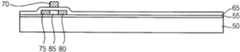
노광된 제1 절연막(5)에 대해 제1 현상 공정 또는 제1 식각 공정을 선택적으로 수행하여 노광된 제1 절연막(5)을 부분적으로 제거함으로써, 제1 절연막(5)에 제1 리세스(recess)(10)를 형성한다. 예시적인 실시예들에 있어서, 제1 리세스(10)는 제1 절연막(5)의 상면으로부터 상대적으로 큰 제1 깊이를 가질 수 있으며, 상대적으로 작은 제1 폭을 가질 수 있다. 또한, 제1 리세스(10)의 측벽은 상기 대상체에 실질적으로 평행한 방향에 대하여 상대적으로 큰 제1 경사각을 가질 수 있다. 예를 들면, 제1 리세스(10) 측벽의 제1 경사각은 상기 대상체에 실질적으로 평행한 축선에 대하여 약 40°내지 약 90°정도가 될 수 있다.The exposed first insulating
도 2를 참조하면, 제1 리세스(10)를 갖는 제1 절연막(5) 상에 제2 절연막(15)을 형성한다. 제2 절연막(15)은 유기 물질, 무기 물질 등을 사용하여 형성될 수 있다. 예를 들면, 제2 절연막(15)은 포토레지스트, 아크릴계 폴리머, 폴리이미드계 폴리머, 폴리아미드계 폴리머, 실록산계 폴리머, 감광성 아크릴 카르복실기를 포함하는 폴리머, 노볼락 수지, 알칼리 가용성 수지, 실리콘 산화물, 실리콘 질화물, 실리콘 산질화물, 실리콘 산탄화물, 실리콘 탄질화물, 알루미늄, 마그네슘, 아연, 하프늄, 지르코늄, 티타늄, 탄탈륨, 알루미늄 산화물, 티타늄 산화물, 탄탈륨 산화물, 마그네슘 산화물, 아연 산화물, 하프늄 산화물, 지르코늄 산화물, 티타늄 산화물 등을 포함할 수 있다. 또한, 제2 절연막(15)은 스핀 코팅 공정, 프린팅 공정, 스퍼터링 공정, 화학 기상 증착 공정, 원자층 적층 공정, 플라즈마 증대 화학 기상 증착 공정, 고밀도 플라즈마-화학 기상 증착 공정, 진공 증착 공정 등을 이용하여 제1 절연막(5) 상에 형성될 수 있다. 예시적인 실시예들에 있어서, 제2 절연막(15)은 제1 절연막(5)과 실질적으로 동일하거나 실질적으로 유사한 물질을 사용하여 형성될 수 있다. 다른 예시적인 실시예들에 따르면, 제1 절연막(5)과 제2 절연막(15)은 서로 상이한 물질들을 사용하여 형성될 수도 있다.Referring to FIG. 2, a second insulating
예시적인 실시예들에 있어서, 제2 절연막(15)은 제1 리세스(10)를 채우지 않으면서 제1 절연막(5) 상에 형성될 수 있다. 즉, 제1 절연막(5)과 제2 절연막(15) 사이에는 제1 리세스(10)가 제2 절연막(15)으로 채워지지 않고 개재될 수 있다. 이러한 구성을 위하여, 제1 리세스(10)의 측벽과 저면에 대하여 표면 처리 공정이 수행될 수 있다. 예를 들면, 제1 리세스(10)의 측벽과 저면에 대하여 선택적으로 플라즈마 처리 공정, 소수성 처리 공정 등을 수행할 수 있다.In the exemplary embodiments, the second insulating
도 3을 참조하면, 제2 절연막(15)에 대하여 차광 영역과 반투과 영역을 갖는 제2 마스크(도시되지 않음)를 이용하는 제2 노광 공정을 수행한 다음, 노광된 제2 절연막(15)에 대해 제2 현상 공정 또는 제2 식각 공정을 수행하여 제2 절연막(15)에 제2 리세스(20)를 형성한다. 상기 제2 마스크는 하프 톤 마스크, 하프 톤 슬릿 마스크 등을 포함할 수 있으며, 상기 차광 영역 및/또는 상기 반투과 영역에 인접하는 투과 영역을 추가적으로 구비할 수도 있다.Referring to FIG. 3, a second exposure process using a second mask (not shown) having a light shielding region and a transflective region is performed on the second insulating
예시적인 실시예들에 있어서, 제2 리세스(20)는 제1 리세스(10)에 연통된다. 제2 리세스(20)는 상대적으로 큰 제2 폭을 가질 수 있고, 상대적으로 작은 제2 깊이를 가질 수 있다. 즉, 제2 리세스(20)의 제2 폭은 제1 리세스(10)의 제1 폭에 비하여 실질적으로 클 수 있는 반면, 제2 리세스(20)의 제2 깊이는 제1 리세스(10)의 제1 깊이보다 실질적으로 작을 수 있다. 또한, 제2 리세스(20)는 제1 절연막(5)에 실질적으로 평행한 방향에 대하여 상대적으로 큰 제2 경사각을 갖는 측벽을 포함할 수 있다. 예를 들면, 제2 리세스(20)의 측벽의 제2 경사각은 상기 대상체에 실질적으로 수평한 축선에 대해 약 40°내지 약 90°정도가 될 수 있다. 즉, 제2 리세스(20)의 측벽의 제2 경사각은 제1 리세스(10)의 측벽의 제1 경사각과 실질적으로 동일하거나 실질적으로 유사할 수 있다. 제1 및 제2 절연막(5, 15)에 각기 제1 및 제2 리세스(10, 20)가 형성됨에 따라 제1 및 제2 절연막(5, 15) 사이에는 단차부(stepped portion)가 제공된다.In the exemplary embodiments, the
도 4를 참조하면, 제1 및 제2 절연막(5, 15)에 대해 리플로우(reflow) 공정을 수행하여 제1 및 제2 리세스(10, 20)로부터 경사 구조(25)를 형성한다. 예시적인 실시예들에 있어서, 상기 리플로우 공정은 제1 및 제2 절연막(5, 15)을 구성하는 물질들의 녹는점(Tm)의 약 50% 내지 약 80% 정도의 온도에서 수행될 수 있다. 예를 들면, 제1 및 제2 절연막(5, 15)의 구성 물질에 따라 제1 및 제2 절연막(5, 15)을 약 100℃ 내지 약 300℃ 정도의 온도에서 약 30분 내지 약 2시간 정도 리플로우시켜 경사 구조(25)를 형성할 수 있다. 이러한 제1 및 제2 절연막(5, 15)의 구성 물질들에 따라 상기 리플로우 공정의 공정 시간과 공정 온도를 조절하여 원하는 측벽 경사각을 갖는 경사 구조(25)를 수득할 수 있다.Referring to FIG. 4, a reflow process is performed on the first and second insulating
예시적인 실시예들에 따른 리플로우 공정에 있어서, 제1 및 제2 절연막(5, 15)이 실질적으로 일체로 결합되면서 상기 대상체 상에 절연층(30)이 형성된다. 즉, 상기 리플로우 공정 동안 제1 및 제2 리세스(10, 20)가 경사 구조(25)로 변화되면서 상기 대상체 상에 경사 구조(25)를 구비하는 절연층(30)이 형성된다.In the reflow process according to the exemplary embodiments, the insulating
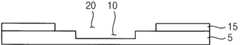
경사 구조(25)는 상대적으로 큰 제3 깊이를 가질 수 있으며, 경사 구조(25)의 측벽은 상대적으로 작은 제3 경사각(θ1)을 가질 수 있다. 즉, 경사 구조(25)의 제3 깊이는 제1 리세스(10)의 제1 깊이 보다 실질적으로 클 수 있다. 예를 들면, 경사 구조(25)의 제3 깊이는 제1 리세스(10)의 제1 깊이와 제2 리세스(20)의 제2 깊이의 합에 실질적으로 대응될 수 있다. 또한, 경사 구조(25)의 측벽의 제3 경사각(θ1)은 제1 리세스(10) 측벽의 제1 경사각 또는 제2 리세스(20) 측벽의 제2 경사각에 비하여 실질적으로 작을 수 있다.The tapered
경사 구조(25)가 제3 경사각(θ1)을 갖는 측벽을 구비함에 따라, 경사 구조(25)는 하부 폭에 비하여 실질적으로 넓은 상부 폭을 가질 수 있다. 예를 들면, 경사 구조(25)의 제3 경사각(θ1)은 상기 대상체에 실질적으로 평행한 방향에 대하여 약 20°내지 약 70°정도가 될 수 있다. 이에 따라, 제1 리세스(10) 측벽의 제1 경사각 또는 제2 리세스(20) 측벽의 제2 경사각과 경사 구조(25)의 측벽의 제3 경사각(θ1) 사이의 비는 약 1.0: 0.2 내지 약 1.0: 1.8 정도가 될 수 있다. 그러나, 이러한 경사 구조(25)의 측벽의 제3 경사각(θ1)은 전술한 리플로우 공정의 공정 시간, 공정 온도 등의 공정 조건들에 따라 변화될 수 있다. 즉, 상기 리플로우 공정의 공정 조건들을 조절하여 경사 구조(25)의 측벽이 원하는 제3 경사각(θ1)을 갖게 할 수 있다.As the tapered
상술한 경사 구조(25)을 갖는 절연층(30)에 광이 입사될 경우, 입사된 광은 제3 경사각(θ1)을 갖는 경사 구조(25)의 측벽에서 반사될 수 있다. 이 때, 경사 구조(25)에 위치하는 다층 구조를 갖는 발광 구조물(도시되지 않음)로부터 발생되는 광이 상기 발광 구조물의 여러 층들 사이 및/또는 상부 혹은 하부의 반사층들 사이에서 전반사가 일어나는 현상을 방지할 수 있도록 경사 구조(25)의 측벽이 제3 경사각(θ1)을 가질 수 있다. 이에 따라, 경사 구조(25) 내에 위치하는 상기 발광 구조물로부터 외부로 방출되는 광의 효율을 향상시킬 수 있다.When light is incident on the insulating
전술한 바에 있어서는, 절연층(30)에 대체적으로 리세스 형상의 경사 구조(25)를 형성하는 과정을 예시적으로 설명하였으나, 다른 예시적인 실시예들에 따라 절연층(30)에 돌출되는 형상의 경사 구조를 형성할 수도 있다. 즉, 도 1 내지 도 4를 참조하여 설명한 공정들과 유사한 공정들을 통해 절연층(30)에 소정의 간격으로 이격된 2개 이상의 리세스 형태를 갖는 경사 구조들이 형성될 경우, 인접하는 리세스 형상의 경사 구조들 사이에는 돌출되는 형상의 경사 구조가 제공될 수 있다. 따라서, 절연층(30)은 돌출되는 형태의 경사 구조를 구비할 수 있다. 다른 예시적인 실시예들에 있어서, 상기 대상체 상에 제1 절연막(5)을 형성한 후, 제1 절연막(5)에 소정의 간격으로 이격되는 제1 리세스들을 형성할 수 있다. 이러한 제1 리세스들을 개재하여 제1 절연막(5) 상에 제2 절연막(15)을 형성한 다음, 상기 제1 리세스들 상부에 위치하는 제2 절연막(15)에 제2 리세스들을 형성할 수 있다. 제1 및 제2 절연막(5, 15)을 리플로우시키면, 절연층(30)에 인접하는 리세스들 사이에 돌출되는 형상의 경사 구조가 형성될 수 있다. 여기서, 상기 돌출되는 형상의 경사 구조의 측벽의 경사각은 상기 리세스 형상의 경사 구조의 측벽의 경사각과 실질적으로 동일하게 된다. 즉, 리세스 형상의 경사 구조와 인접하는 돌출되는 형상의 경사 구조가 하나의 측벽을 공유할 수 있다.In the above description, the process of forming the generally tapered recessed
도 5 내지 도 11은 본 발명의 예시적인 실시예들에 따라 경사 구조를 갖는 절연층을 포함하는 유기 발광 표시 장치의 제조 방법을 설명하기 위한 단면도들이다.5 to 11 are cross-sectional views illustrating a method of manufacturing an organic light emitting display including an insulating layer having a tilted structure according to exemplary embodiments of the present invention.
도 5를 참조하면, 제1 기판(50) 상에 버퍼층(55)을 형성한다. 제1 기판(50)은 투명 절연 기판을 포함할 수 있다. 예를 들면, 제1 기판(50)은 유리 기판, 석영 기판, 투명 수지 기판 등으로 이루어질 수 있다. 제1 기판(50)으로 사용될 수 있는 투명 수지 기판은 폴리이미드 수지, 아크릴 수지, 폴리아크릴레이트 수지, 폴리카보네이트 수지, 폴리에테르 수지, 폴리에틸렌 테레프탈레이트 수지, 술폰산 수지 등을 포함할 수 있다.Referring to FIG. 5, a
다른 예시적인 실시예들에 있어서, 제1 기판(50) 상에 버퍼층(55)을 형성하기 전에 제1 기판(50)에 대하여 평탄화 공정을 수행할 수 있다. 예를 들면, 화학 기계적 연마 공정 및/또는 에치 백 공정을 제1 기판(50)에 대해 수행하여 제1 기판(50)이 실질적으로 평탄한 상면을 확보할 수 있다. 또 다른 예시적인 실시예들에 따르면, 제1 기판(50)의 표면 평탄도, 구성 물질 등에 따라 제1 기판(50) 상에 버퍼층(55)이 형성되지 않을 수도 있다.In other exemplary embodiments, a planarization process may be performed with respect to the
버퍼층(55)은 제1 기판(50)으로부터 금속 원자들, 불순물들 등이 확산되는 현상을 방지하는 기능을 수행할 수 있으며, 버퍼층(55)으로 인하여 후속하는 반도체 패턴(60)을 형성하기 위한 결정화 공정 동안 열의 전달 속도가 조절되어 실질적으로 균일한 반도체 패턴(60)을 수득할 수 있다. 또한, 버퍼층(55)은 제1 기판(50)이 표면이 균일하지 않을 경우, 제1 기판(50)의 표면의 평탄도를 향상시키는 역할도 수행할 수 있다. 버퍼층(55)은 실리콘 화합물을 사용하여 형성될 수 있다. 예를 들면, 버퍼층(55)은 실리콘 산화물, 실리콘 질화물, 실리콘 산질화물, 실리콘 산탄화물, 실리콘 탄질화물 등을 포함할 수 있다. 이들은 단독으로 또는 서로 조합되어 사용될 수 있다. 다른 예시적인 실시예들에 있어서, 버퍼층(55)은 실리콘 화합물을 포함하는 단층 구조 또는 다층 구조를 가질 수 있다. 예를 들면, 버퍼층(55)은 실리콘 산화막, 실리콘 질화막, 실리콘 산질화막, 실리콘 산탄화막 및/또는 실리콘 탄질화막을 포함할 수 있다.The
버퍼층(55) 상에는 반도체 패턴(60)이 형성된다. 예시적인 실시예들에 있어서, 버퍼층(55) 상에 반도체층(도시되지 않음)을 형성한 후, 이러한 반도체층을 패터닝하여 버퍼층(55)의 일측 상에 예비 반도체 패턴(도시되지 않음)을 형성할 수 있다. 다음에, 상기 예비 반도체 패턴을 결정화시켜 버퍼층(55) 상에 반도체 패턴(60)을 수득할 수 있다. 상기 반도체층은 화학 기상 증착 공정, 플라즈마 증대 화학 기상 증착 공정, 저압 화학 기상 증착 공정, 스퍼터링 공정 등을 이용하여 형성될 수 있다. 상기 반도체층이 아몰퍼스 실리콘을 포함할 경우, 반도체 패턴(60)은 폴리실리콘으로 이루어질 수 있다. 여기서, 상기 예비 반도체 패턴으로부터 반도체 패턴(60)을 형성하기 위한 결정화 공정은 레이저 조사 공정, 열처리 공정, 촉매를 이용하는 열처리 공정 등을 포함할 수 있다.A
다른 예시적인 실시예들에 따르면, 상기 반도체층 및/또는 상기 예비 반도체 패턴을 형성한 후, 상기 반도체층 및/또는 상기 예비 반도체 패턴에 대하여 탈수소(dehydrogenation) 공정을 수행할 수 있다. 이에 따라, 상기 반도체층 및/또는 상기 예비 반도체 패턴 내의 수소 원자들의 농도를 감소시켜, 반도체 패턴(60)의 전기적인 특성을 향상시킬 수 있다.According to other exemplary embodiments, a dehydrogenation process may be performed on the semiconductor layer and / or the preliminary semiconductor pattern after the semiconductor layer and / or the preliminary semiconductor pattern are formed. Accordingly, the concentration of hydrogen atoms in the semiconductor layer and / or the preliminary semiconductor pattern can be reduced, thereby improving the electrical characteristics of the
도 6을 참조하면, 버퍼층(55) 상에 반도체 패턴(60)을 커버하는 게이트 절연막(65)을 형성한다. 게이트 절연막(65)은 화학 기상 증착 공정, 스핀 코팅 공정, 플라즈마 증대 화학 기상 증착 공정, 스퍼터링 공정, 진공 증착 공정, 고밀도 플라즈마-화학 기상 증착 공정, 프린팅 공정 등을 이용하여 형성될 수 있다. 또한, 게이트 절연막(65)은 실리콘 산화물, 금속 산화물 등을 사용하여 형성될 수 있다. 게이트 절연막(65)에 사용될 수 있는 금속 산화물은, 하프늄 산화물(HfOx), 알루미늄 산화물(AlOx) 지르코늄 산화물(ZrOx), 티타늄 산화물(TiOx), 탄탈륨 산화물(TaOx) 등을 포함할 수 있다. 이들은 단독으로 또는 서로 조합되어 사용될 수 있다.Referring to FIG. 6, a
게이트 절연막(65)은 반도체 패턴(60)의 프로파일(profile)을 따라 버퍼층(55) 상에 실질적으로 균일하게 형성될 수 있다. 게이트 절연막(65)은 상대적으로 얇은 두께를 가질 수 있으며, 게이트 절연막(65)에는 반도체 패턴(60)에 인접하는 단차부가 생성될 수 있다. 다른 예시적인 실시예들에 따르면, 게이트 절연막(65)은 반도체 패턴(60)을 충분히 커버하면서 실질적으로 평탄한 상면을 가질 수 있다. 이 경우, 게이트 절연막(65)은 상대적으로 두꺼운 두께를 가질 수 있다.The
게이트 절연막(65) 상에는 게이트 전극(70)이 형성된다. 게이트 전극(70)은 게이트 절연막(65) 중에서 아래에 반도체 패턴(60)이 위치하는 부분 상에 형성한다. 예시적인 실시예들에 있어서, 게이트 절연막(65) 상에 제1 도전막(도시되지 않음)을 형성한 후, 사진 식각 공정 또는 추가적인 식각 마스크를 이용하는 식각 공정 등을 통해 상기 제1 도전막을 패터닝함으로써, 게이트 절연막(65) 상에 게이트 전극(70)을 형성할 수 있다. 상기 제1 도전막은 스퍼터링 공정, 화학 기상 증착 공정, 펄스 레이저 증착 공정, 진공 증착 공정, 원자층 적층 공정, 프린팅 공정 등을 이용하여 형성될 수 있다.A
게이트 전극(70)은 금속, 합금, 금속 질화물, 도전성 금속 산화물, 투명 도전성 물질 등을 포함할 수 있다. 예를 들면, 게이트 전극(70)은 알루미늄(Al), 알루미늄을 함유하는 합금, 알루미늄 질화물(AlNx), 은(Ag), 은을 함유하는 합금, 텅스텐(W), 텅스텐 질화물(WNx), 구리(Cu), 구리를 함유하는 합금, 니켈(Ni), 크롬(Cr), 크롬 질화물(CrOx), 몰리브데늄(Mo), 몰리브데늄을 함유하는 합금, 티타늄(Ti), 티타늄 질화물(TiNx), 백금(Pt), 탄탈륨(Ta), 탄탈륨 질화물(TaNx), 네오디뮴(Nd), 스칸듐(Sc), 스트론튬 루테늄 산화물(SrRuxOy), 아연 산화물(ZnOx), 인듐 주석 산화물(ITO), 주석 산화물(SnOx), 인듐 산화물(InOx), 갈륨 산화물(GaOx), 인듐 아연 산화물(IZO) 등을 포함할 수 있다. 이들은 단독으로 또는 서로 조합되어 사용될 수 있다. 예시적인 실시예들에 따르면, 게이트 전극(70)은 상술한 금속, 합금, 금속 질화물, 도전성 금속 산화물 또는 투명 도전성 물질로 이루어진 단층 구조를 가질 수 있다. 이와는 달리, 게이트 전극(70)은 전술한 금속, 합금, 금속 질화물, 도전성 금속 산화물 및/또는 투명 도전성 물질로 구성된 다층 구조로 형성될 수도 있다.The
도 6에 도시하지는 않았으나, 게이트 전극(70)의 형성과 동시에 게이트 절연막(65) 일측 상에는 게이트 라인이 형성된다. 게이트 전극(70)은 이와 같은 게이트 라인에 연결되며, 상기 게이트 라인은 게이트 절연막(65) 상에서 제1 방향을 따라 연장될 수 있다.Although not shown in FIG. 6, a gate line is formed on one side of the
게이트 전극(70)을 주입 마스크로 이용하여 반도체 패턴(60)에 불순물들을 주입함으로써, 반도체 패턴(60)에 소스 영역(75)과 드레인 영역(80)을 형성한다. 상기 불순물들의 주입을 위한 이온 주입 에너지의 조절에 따라 상기 불순물들이 게이트 절연막(65)을 통과하여 반도체 패턴(60)의 양측부에 주입될 수 있다. 여기서, 게이트 전극(70) 아래에 위치하는 반도체 패턴(60)의 중앙부에는 상기 불순물들이 주입되지 않으며, 이에 따라 반도체 패턴(60)의 중앙부는 소스 영역(75)과 드레인 영역 사이의 채널 영역(85)이 된다. 다시 말하면, 소스 및 드레인 영역(75, 80)의 형성에 따라 반도체 패턴(60)에 채널 영역(85)이 정의된다. 다른 예시적인 실시예들에 따르면, 게이트 절연막(65) 상에 게이트 전극(70)에 인접하는 게이트 절연막(65)의 부분들을 노출시키는 마스크를 형성한 다음, 이와 같은 마스크와 게이트 전극(70)을 함께 주입 마스크들로 이용하여 소스 영역(75) 및 드레인 영역(80)을 형성할 수도 있다.A
예시적인 실시예들에 있어서, 게이트 전극(70)은 반도체 패턴(60)에 비하여 실질적으로 작은 폭을 가질 수 있다. 예를 들면, 게이트 전극(70)은 채널 영역(85)과 실질적으로 동일하거나 실질적으로 유사한 폭을 가질 수 있다. 그러나, 게이트 전극(70)의 치수 및/또는 채널 영역(85)의 치수는 이들을 포함하는 스위칭 소자에 요구되는 전기적인 특성에 따라 변화될 수 있다.In the exemplary embodiments, the
도 7을 참조하면, 게이트 절연막(65) 상에 게이트 전극(70)을 덮는 층간 절연막(90)을 형성한다. 층간 절연막(90)은 게이트 전극(70)의 프로파일을 따라 게이트 절연막(65) 상에 실질적으로 균일한 두께로 형성될 수 있다. 따라서, 층간 절연막(90)에는 게이트 전극(70)에 인접하는 단차부가 생성될 수 있다. 층간 절연막(90)은 실리콘 화합물을 사용하여 형성될 수 있다. 예를 들면, 층간 절연막(90)은 실리콘 산화물, 실리콘 질화물, 실리콘 산질화물, 실리콘 탄질화물, 실리콘 산탄화물 등을 사용하여 형성될 수 있다. 이들은 단독으로 또는 서로 조합되어 사용될 수 있다. 또한, 층간 절연막(90)은 전술한 실리콘 산화물, 실리콘 질화물, 실리콘 산질화물, 실리콘 탄질화물, 실리콘 산탄화물 등을 포함하는 단층 구조 또는 다층 구조를 가질 수 있다. 이 경우, 층간 절연막(90)은 스핀 코팅 공정, 화학 기상 증착 공정, 플라즈마 증대 화학 기상 증착 공정, 고밀도 플라즈마-화학 기상 증착 공정 등을 이용하여 수득될 수 있다. 층간 절연막(90)은 후속하여 형성되는 소스 전극(95)과 드레인 전극(100)으로부터 게이트 전극(70)을 절연시키는 역할을 수행할 수 있다.Referring to FIG. 7, an
층간 절연막(90) 상에 소스 전극(95)과 드레인 전극(100)을 형성한다. 소스 및 드레인 전극(95, 100)은 게이트 전극(70)을 중심으로 소정의 간격으로 이격되며, 게이트 전극(70)에 인접하여 배치된다. 예를 들면, 소스 및 드레인 전극(95, 100)은 각기 소스 및 드레인 영역(75, 80) 상부에 위치하는 층간 절연막(90)으로부터 게이트 전극(70) 상에 위치하는 층간 절연막(90)까지 연장될 수 있다. 또한, 소스 및 드레인 전극(95, 100)은 층간 절연막(90)을 관통하여 소스 및 드레인 영역(75, 80)에 각기 접촉된다.A
예시적인 실시예들에 있어서, 층간 절연막(90)을 부분적으로 식각하여 소스 및 드레인 영역(75, 80)을 부분적으로 노출시키는 홀들을 형성한 후, 이러한 홀들을 채우면서 층간 절연막(90) 상에 제2 도전막(도시되지 않음)을 형성한다. 다음에, 상기 제2 도전막을 패터닝하여 도 7에 예시적으로 도시한 바와 같은 소스 및 드레인 전극(95, 100)을 형성한다. 상기 제2 도전막은 스퍼터링 공정, 화학 기상 증착 공정, 펄스 레이저 증착 공정, 진공 증착 공정, 원자층 적층 공정, 프린팅 공정 등을 이용하여 수득될 수 있다. 소스 및 드레인 전극(95, 100)은 각기 금속, 합금, 금속 질화물, 도전성 금속 산화물, 투명 도전성 물질 등을 포함할 수 있다. 예를 들면, 소스 및 드레인 전극(95, 100)은 각기 알루미늄, 알루미늄을 함유하는 합금, 알루미늄 질화물, 은, 은을 함유하는 합금, 텅스텐, 텅스텐 질화물, 구리, 구리를 함유하는 합금, 니켈, 크롬, 크롬 질화물, 몰리브데늄, 몰리브데늄을 함유하는 합금, 티타늄, 티타늄 질화물, 백금, 탄탈륨, 탄탈륨 질화물, 네오디뮴, 스칸듐, 스트론튬 루테늄 산화물, 아연 산화물, 인듐 주석 산화물, 주석 산화물, 인듐 산화물, 갈륨 산화물, 인듐 아연 산화물 등으로 이루어질 수 있다. 이들은 단독으로 또는 서로 조합되어 사용될 수 있다. 한편, 소스 및 드레인 전극(95, 100)은 각기 전술한 금속, 합금, 금속 질화물, 도전성 금속 산화물, 투명 도전성 물질 등으로 이루어진 단층 구조 또는 다층 구조를 가질 수 있다.In the illustrative embodiments, the
도시하지는 않았으나, 층간 절연막(90) 상에는 제2 방향을 따라 연장되는 데이터 라인이 소스 및 드레인 전극(95, 100)과 함께 형성된다. 여기서, 상기 제2 방향은 상기 게이트 라인이 연장되는 제1 방향과 실질적으로 직교할 수 있다. 이와 같은 데이터 라인에 소스 전극(95)이 접속된다.Although not shown, a data line extending along the second direction is formed on the
층간 절연막(90) 상에 소스 및 드레인 전극(95, 100)이 형성됨에 따라, 제1 기판(50) 상에는 상기 유기 발광 표시 장치의 스위칭 소자로서 반도체 패턴(60), 게이트 절연막(65), 게이트 전극(70), 소스 전극(95) 및 드레인 전극(100)을 포함하는 박막 트랜지스터(TFT)가 제공된다.The source and drain
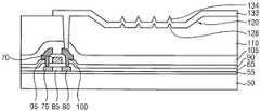
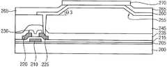
도 8을 참조하면, 층간 절연막(90) 상에 소스 및 드레인 전극(95, 100)을 커버하는 제1 보호막(105)을 형성한다. 제1 보호막(105)은 소스 및 드레인 전극(95, 100)을 완전하게 덮을 수 있는 충분한 두께를 가질 수 있다. 제1 보호막(105)은 유기 물질, 무기 물질 등을 사용하여 형성될 수 있다. 예를 들면, 제1 보호막(105)은 포토레지스트, 아크릴계 폴리머, 폴리이미드계 폴리머, 폴리아미드계 폴리머, 실록산계 폴리머, 감광성 아크릴 카르복실기를 포함하는 폴리머, 노볼락 수지, 알칼리 가용성 수지, 실리콘 산화물, 실리콘 질화물, 실리콘 산질화물, 실리콘 산탄화물, 실리콘 탄질화물, 알루미늄, 마그네슘, 아연, 하프늄, 지르코늄, 티타늄, 탄탈륨, 알루미늄 산화물, 티타늄 산화물, 탄탈륨 산화물, 마그네슘 산화물, 아연 산화물, 하프늄 산화물, 지르코늄 산화물, 티타늄 산화물 등을 포함할 수 있다. 이들은 단독으로 또는 서로 조합되어 사용될 수 있다. 제1 보호막(105)을 구성하는 물질에 따라 제1 보호막(105)은 스핀 코팅 공정, 프린팅 공정, 스퍼터링 공정, 화학 기상 증착 공정, 원자층 적층 공정, 플라즈마 증대 화학 기상 증착 공정, 고밀도 플라즈마-화학 기상 증착 공정, 진공 증착 공정, 프린팅 공정 등을 이용하여 수득될 수 있다. 다른 예시적인 실시예들에 따르면, 후속하여 형성되는 절연층(110)의 구성 물질, 치수 등에 따라 상기 스위칭 소자를 커버하는 제1 보호막(105)이 제공되지 않을 수도 있다.Referring to FIG. 8, a first
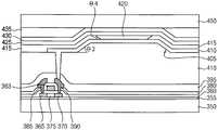
도 8 및 도 9를 참조하면, 제1 보호막(105) 상에는 경사 구조(120)를 갖는 절연층(110)이 형성된다. 절연층(110)은 단층 구조로 형성될 수 있지만, 적어도 2이상의 절연막들을 포함하는 다층 구조로 형성될 수도 있다. 예시적인 실시예들에 있어서, 절연층(110)은 제1 보호막(105) 상에 순차적으로 형성된 제1 절연막 및 제2 절연막을 포함할 수 있다. 이러한 제1 및 제2 절연막을 포함하는 절연층(110)을 형성하기 위한 공정들은 각기 도 1 및 도 2를 참조하여 설명한 제1 및 제2 절연막(5, 15)을 형성하는 공정들과 실질적으로 동일하거나 실질적으로 유사하다. 또한, 절연층(110)의 제1 및 제2 절연막은 각기 도 1 및 도 2를 참조하여 설명한 제1 및 제2 절연막(5, 15)과 실질적으로 동일하거나 실질적으로 유사한 물질을 포함할 수 있다.Referring to FIGS. 8 and 9, an insulating
도 8 및 도 9에 도시한 바와 같이, 절연층(110)에는 측벽이 제4 경사각(θ2)을 갖는 경사 구조(120)가 형성된다. 또한, 절연층(110)과 제1 보호막(105)을 관통하여 드레인 전극(100)을 부분적으로 노출시키는 홀(115)이 형성된다. 예시적인 실시예들에 있어서, 홀(115)은 절연층(110)에 경사 구조(120)를 형성하는 동안 형성될 수 있다. 다른 예시적인 실시예들에 따르면, 절연층(110)에 경사 구조(120)를 형성한 후, 절연층(110)과 제1 보호막(105)을 관통하여 드레인 전극(100)의 일부를 노출시키는 홀(115)을 형성할 수도 있다.As shown in FIGS. 8 and 9, the insulating
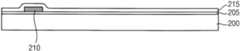
절연층(110)의 경사 구조(120)는 도 1 내지 도 4를 참조하여 설명한 절연층(30)의 경사 구조(25)를 형성하는 공정들과 실질적으로 동일하거나 실질적으로 유사한 공정들을 이용하여 형성될 수 있다. 또한, 절연층(110)의 경사 구조(120) 측벽의 제4 경사각(θ2)은 상술한 경사 구조(25)의 측벽의 제3 경사각(θ1)과 실질적으로 동일하거나 실질적으로 유사할 수 있다. 예를 들면, 경사 구조(120)의 측벽의 제4 경사각(θ2)은 제1 기판(50)에 실질적으로 평행한 축선에 대하여 약 20°내지 약 70°정도가 될 수 있다.The tapered
도 9에 예시한 바와 같이, 절연층(110)에는 리세스 형상(recessed shape)을 갖는 경사 구조(120)가 형성된다. 절연층(110)의 경사 구조(120)가 이와 같은 리세스 형상을 가질 경우, 경사 구조(120)를 갖는 절연층(110)을 포함하는 상기 유기 발광 표시 장치는 전면 발광 방식을 가질 수 있다.As illustrated in FIG. 9, the insulating
도 10을 참조하면, 경사 구조(120)를 갖는 절연층(110) 상에 홀(115)을 채우면서 제1 전극(125)을 형성한다. 제1 전극(125)은 드레인 전극(100)에 접속되며, 경사 구조(120)의 측벽과 저면 상으로 연장된다. 이에 따라, 경사 구조(120) 내에 위치하는 제1 전극(125)의 측부도 경사 구조(120)의 제4 경사각(θ2)과 실질적으로 동일하거나 실질적으로 유사한 경사각을 가질 수 있다. 예를 들면, 경사 구조(120) 내에서의 제1 전극(125) 측부의 경사각은 제1 기판(50)에 실질적으로 평행한 방향에 대해 약 20°내지 약 70°정도가 될 수 있다.Referring to FIG. 10, a
상기 유기 발광 표시 장치가 전면 발광 방식을 가질 경우, 제1 전극(125)은 반사성을 갖는 물질을 사용하여 형성될 수 있다. 예를 들면, 제1 전극(125)은 알루미늄, 은, 백금, 금(Au), 크롬, 텅스텐, 몰리브데늄, 티타늄, 팔라듐(Pd), 이리듐(Ir) 등과 같은 금속, 이들의 합금 등을 포함할 수 있다. 이들은 단독으로 또는 서로 조합되어 사용될 수 있다. 또한, 제1 전극(125)은 전술한 금속 및/또는 합금을 포함하는 단층 구조 또는 다층 구조로 형성될 수 있다.When the organic light emitting display device has a front emission type, the
예시적인 실시예들에 있어서, 드레인 전극(100)을 노출시키는 홀(115)을 채우면서 절연층(110) 상에 제1 전극층(도시되지 않음)을 형성한 다음, 이와 같은 제1 전극층을 패터닝하여, 경사 구조(120)를 갖는 절연층(110) 상에 제1 전극(125)을 형성할 수 있다. 여기서, 상기 제1 전극층은 제1 전극(125)을 구성하는 물질에 따라 스퍼터링 공정, 진공 증착 공정, 화학 기상 증착 공정, 펄스 레이저 증착 공정, 프린팅 공정, 원자층 적층 공정 등을 이용하여 형성될 수 있다. 후술하는 바와 같이, 제1 전극(125)은 상기 유기 발광 표시 장치의 발광 영역(luminescent region)을 중심으로 인접하는 비발광 영역(non-luminescent region)의 일부까지 연장될 수 있다.In the exemplary embodiments, a first electrode layer (not shown) is formed on the insulating
다른 예시적인 실시예들에 따르면, 절연층(110) 및 제1 보호막(105)을 관통하는 홀(115)의 내부와 노출된 드레인 전극(100) 상에 콘택 구조물 또는 패드 구조물 등을 형성한 후, 절연층(110) 상에 상기 콘택 구조물 또는 상기 패드 구조물에 접속되는 제1 전극(125)을 형성할 수도 있다. 이 경우, 제1 전극(125)은 상기 콘택 구조물 또는 상기 패드 구조물을 통해 드레인 전극(100)에 전기적으로 연결될 수 있다.According to other exemplary embodiments, after a contact structure or a pad structure is formed on the inside of the
다시 도 10을 참조하면, 절연층(110)과 제1 전극(125) 상에 화소 정의막(130)을 형성한다. 화소 정의막(130)은 유기 물질, 무기 물질 등을 사용하여 형성될 수 있다. 예를 들면, 화소 정의막(130)은 포토레지스트, 폴리아크릴계 수지, 폴리이미드계 수지, 아크릴계 수지 등의 유기 물질이나 실리콘 화합물과 같은 무기 물질을 포함할 수 있다.Referring again to FIG. 10, a
화소 정의막(130)을 부분적으로 식각하여 제1 전극(125)의 일부를 노출시키는 개구를 형성한다. 예를 들면, 상기 개구는 사진 식각 공정이나 추가적인 식각 마스크를 사용하는 식각 공정을 이용하여 형성될 수 있다. 예시적인 실시예들에 있어서, 화소 정의막(130)의 개구의 측벽은 경사 구조(120)의 제4 경사각(θ2)과 실질적으로 동일하거나 실질적으로 유사한 경사각을 가질 수 있다. 예를 들면, 화소 정의막(130)의 개구의 측벽은 제1 기판(50)에 실질적으로 수평한 방향에 대해 약 20°내지 약 70°정도의 경사각을 가질 수 있다.The
화소 정의막(130)에 개구가 형성됨에 따라, 상기 유기 발광 표시 장치의 발광 영역과 비발광 영역이 정의된다. 즉, 화소 정의막(130)의 개구가 위치하는 영역이 상기 발광 영역에 해당되며, 상기 개구에 인접하는 영역이 상기 비발광 영역에 해당된다. 절연층(110)의 경사 구조(120)는 상기 발광 영역에 위치하며, 상기 발광 영역에서 제1 전극(125)은 경사 구조(120)의 저면과 측벽 상에 실질적으로 균일하게 형성될 수 있다. 화소 정의막(130)은 상기 발광 영역의 일부까지 연장되어 경사 구조(120)의 저면의 일부와 측벽 상부에 형성된다. 다시 말하면, 상기 발광 영역에서 화소 정의막(130)은 제1 전극(125)의 측부를 커버한다. 이에 따라, 상기 발광 영역에 위치하는 화소 정의막(130)의 일부(즉, 상기 개구의 측벽)도 경사 구조(120)의 제4 경사각(θ2)과 실질적으로 동일하거나 실질적으로 유사한 경사각을 가질 수 있다. 예를 들면, 상기 발광 영역에 위치하는 화소 정의막(130)은 제1 기판(50)에 실질적으로 평행한 축선에 대해 약 20°내지 약 70°정도의 경사각을 가지면서 제1 전극(125) 상에 배치될 수 있다.As the opening is formed in the
상기 발광 영역의 화소 정의막(130) 및 제1 전극(125) 상에 유기 발광 구조물(135)이 형성된다. 예시적인 실시예들에 있어서, 유기 발광 구조물(135)은 유기 발광층(EL), 정공 주입층(HIL), 정공 수송층(HTL), 전자 수송층(ETL), 전자 주입층(EIL) 등을 포함하는 다층 구조를 가질 수 있다. 유기 발광 구조물(135)은 상기 유기 발광 표시 장치의 각 화소에 따라 적색광, 녹색광, 청색광 등과 같은 서로 다른 색광들을 발생시킬 수 있는 발광 물질들을 사용하여 형성될 수 있다. 다른 예시적인 실시예들에 있어서, 유기 발광 구조물(135)은 적색광, 녹색광, 청색광 등의 상이한 색광들을 구현할 수 있는 복수의 발광 물질들이 적층되어 백색광을 발광하는 다층 구조를 가질 수도 있다. 또 다른 예시적인 실시예들에 따르면, 유기 발광 구조물(135)은 상기 발광 물질들에 비하여 실질적으로 큰 밴드 갭(band gap)을 갖는 호스트 물질을 추가적으로 포함할 수 있다.An organic
예시적인 실시예들에 있어서, 유기 발광 구조물(135)은 상기 발광 영역의 경사 구조(120) 상에 위치한다. 또한, 유기 발광 구조물(135)은 상기 발광 영역에서 제1 전극(125) 및 화소 정의막(130)에 접촉된다. 즉, 유기 발광 구조물(135)의 저면은 제1 전극(125) 상에 위치하며, 유기 발광 구조물(135)의 측부는 화소 정의막(130)에 접촉된다. 따라서, 유기 발광 구조물(135)의 측부도 경사 구조(120)의 측벽의 제4 경사각(θ2)과 실질적으로 동일하거나 실질적으로 유사한 경사각을 가질 수 있다. 예를 들면, 유기 발광 구조물(135)의 측부는 제1 기판(50)에 대해 실질적으로 평행한 축선에 대하여 약 20°내지 약 70°정도의 경사각을 가질 수 있다.In the exemplary embodiments, the organic
제2 전극(140)은 유기 발광 구조물(135)과 화소 정의막(130) 상에 형성된다. 제2 전극(140)은 유기 발광 구조물(135)과 화소 정의막(130) 상에 균일한 두께로 형성될 수 있다. 상기 유기 발광 표시 장치가 전면 발광 방식을 가질 경우, 제2 전극(140)은 투명 도전성 물질을 사용하여 형성될 수 있다. 예를 들면, 제2 전극(140)은 인듐 주석 산화물, 인듐 아연 산화물, 아연 주석 산화물, 아연 산화물, 주석 산화물, 갈륨 산화물 등을 포함할 수 있다. 이들은 단독으로 또는 서로 조합되어 사용될 수 있다.The
예시적인 실시예들에 있어서, 제2 전극(140)은 상기 발광 영역으로부터 상기 비발광 영역까지 연장될 수 있다. 다른 예시적인 실시예들에 따르면, 제2 전극(140)은 상기 발광 영역에만 위치할 수도 있다. 예를 들면, 제2 전극(140)은 유기 발광 구조물(135)과 화소 정의막(130)의 일부(즉, 화소 정의막(130)의 개구의 측벽) 상에 배치될 수 있다. 이 경우, 유기 발광 구조물(135)과 화소 정의막(130) 상에 제2 전극층(도시되지 않음)을 형성한 후, 상기 제2 전극층을 패터닝하여 상기 발광 영역에 제2 전극(140)을 형성할 수 있다.In the exemplary embodiments, the
절연층(110)의 경사 구조(120) 측벽의 제4 경사각(θ2)에 따라 제2 전극(140)도 상기 발광 영역에서 제4 경사각(θ2)과 실질적으로 동일하거나 실질적으로 유사한 경사각을 가질 수 있다. 예를 들면, 상기 발광 영역의 화소 정의막(130) 상에 위치하는 제2 전극(140)의 측부는 제1 기판(50)에 실질적으로 평행한 축선에 대해 약 20°내지 약 70°정도의 경사각을 가질 수 있다.The
하부 전극, 유기 발광층 및 상부 전극을 구비하는 종래의 유기 발광 표시 장치에 있어서, 상기 유기 발광층으로부터 발생되는 광이 상기 유기 발광층과 상기 상부 및 하부 전극 사이에서 전반사되어 실질적으로 약 30% 정도의 광 손실(loss)이 발생하게 된다. 이에 비하여, 본 발명의 예시적인 실시예들에 따르면, 리세스 형상을 갖는 경사 구조(120)로 인하여 유기 발광 구조물(135), 제1 전극(125) 및 제2 전극(140)의 측부들이 각기 유기 발광 구조물(135)로부터 발생되는 광의 전반사를 방지할 수 있는 경사각을 가지기 때문에, 상기 유기 발광 표시 장치는 종래의 유기 발광 표시 장치에 비하여 적어도 약 30% 이상 증가된 광 효율을 확보할 수 있다. 또한, 예시적인 실시예들에 따른 유기 발광 표시 장치는, 유기 발광 구조물(135)로부터 발생되는 광의 광학적 공진을 위하여 상대적으로 복잡한 구성을 가질 필요가 없기 때문에, 광학적 공진 구조를 갖는 종래의 유기 발광 표시 장치에 비하여 보다 간단한 구성을 가질 수 있으며, 보다 향상된 측면 시인성을 확보할 수 있다.In the conventional organic light emitting diode display having a lower electrode, an organic light emitting layer and an upper electrode, light generated from the organic light emitting layer is totally reflected between the organic light emitting layer and the upper electrode and the lower electrode, a loss occurs. In contrast, according to exemplary embodiments of the present invention, the sides of the organic
도 11을 참조하면, 제2 전극(140) 상에 제2 보호막(145)을 형성한다. 제2보호막(145)은 상기 발광 영역으로부터 상기 비발광 영역까지 연장될 수 있다. 제2 보호막(145)은 유기 물질, 무기 물질 등을 사용하여 형성될 수 있다. 예를 들면, 제2 보호막(145)은 포토레지스트, 아크릴계 폴리머, 폴리이미드계 폴리머, 폴리아미드계 폴리머, 실록산계 폴리머, 감광성 아크릴 카르복실기를 포함하는 폴리머, 노볼락 수지, 알칼리 가용성 수지, 실리콘 산화물, 실리콘 질화물, 실리콘 산질화물, 실리콘 산탄화물, 실리콘 탄질화물, 알루미늄, 마그네슘, 아연, 하프늄, 지르코늄, 티타늄, 탄탈륨, 알루미늄 산화물, 티타늄 산화물, 탄탈륨 산화물, 마그네슘 산화물, 아연 산화물, 하프늄 산화물, 지르코늄 산화물, 티타늄 산화물 등을 포함할 수 있다. 이들은 단독으로 또는 서로 조합되어 사용될 수 있다. 제2 보호막(145)을 구성하는 물질에 따라, 제2 보호막(145)은 스핀 코팅 공정, 프린팅 공정, 스퍼터링 공정, 화학 기상 증착 공정, 원자층 적층 공정, 플라즈마 증대 화학 기상 증착 공정, 고밀도 플라즈마-화학 기상 증착 공정, 진공 증착 공정 등을 이용하여 수득될 수 있다.Referring to FIG. 11, a second
제2 보호막(145) 상에는 제2 기판(150)이 배치된다. 제2 기판(150)은 유리, 투명 플라스틱, 투명 세라믹 등과 같은 투명 절연 기판을 포함할 수 있다. 예시적인 실시예들에 있어서, 상기 발광 영역의 제2 보호막(145)과 제2 기판(150) 사이의 공간(148)은 공기 또는 질소와 같은 불활성 기체 등으로 채워질 수 있다. 다른 예시적인 실시예들에 따르면, 상기 발광 영역의 공간(148)은 광 투과성과 흡습성을 갖는 수지로 충진될 수도 있다.A
도 12 및 도 13은 본 발명의 다른 예시적인 실시예들에 따른 유기 발광 표시 장치의 제조 방법을 설명하기 위한 단면도들이다. 도 12 및 도 13에 있어서, 절연층, 제1 전극, 유기 발광 구조물 등을 제외하면 도 5 내지 도 11을 참조하여 설명한 유기 발광 표시 장치와 실질적으로 동일하거나 실질적으로 유사한 구성을 가지는 유기 발광 표시 장치의 제조 방법을 예시적으로 설명하지만, 도 12 및 도 13에 도시한 제조 방법은 스위칭 소자, 보호막(들), 전극들, 절연층(들), 유기 발광 구조물 등이 다양한 구조로 배치된 구성을 가지는 다른 유기 발광 표시 장치들에도 해당 기술 분야에서 통상의 지식을 가진 자에게 자명한 변경이 적용 가능함을 이해할 수 있을 것이다.12 and 13 are cross-sectional views illustrating a method of manufacturing an organic light emitting display according to another exemplary embodiment of the present invention. 12 and 13, an organic light emitting display device having substantially the same or substantially similar structure as the organic light emitting display device described with reference to FIGS. 5 to 11, except for an insulating layer, a first electrode, The manufacturing method shown in FIG. 12 and FIG. 13 exemplifies a structure in which a switching element, a protective film (s), electrodes, an insulating layer (s), an organic light emitting structure, It will be understood that modifications obvious to those skilled in the art may be applied to other organic light emitting display devices.
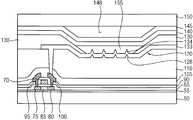
도 12를 참조하면, 도 7 및 도 8을 참조하여 설명한 공정들과 실질적으로 동일하거나 실질적으로 유사한 공정들을 수행하여 제1 기판(50) 상에 버퍼층(55), 스위칭 소자, 제1 보호막(105) 등을 형성한다.Referring to FIG. 12, a
제1 보호막(105) 상에 경사 구조(120)와 드레인 전극(100)의 일부를 노출시키는 홀을 포함하는 절연층(110)을 형성한 후, 경사 구조(120)의 저면을 구성하는 절연층(110)에 복수의 돌기(128)들을 형성한다. 절연층(110)의 경사 구조(120)는 도 1 내지 도 4를 참조하여 설명한 공정들과 실질적으로 동일하거나 실질적으로 유사한 공정들을 수행하여 수득될 수 있다. 예시적인 실시예들에 있어서, 절연층(110)의 돌기(128)들은 경사 구조(120)의 저면을 구성하는 절연층(110)의 표면에 대하여 추가적으로 하프 톤 마스크 또는 하프 톤 슬릿 마스크를 사용하는 노광 공정, 현상 공정, 부분 식각 공정 등을 수행하여 수득될 수 있다. 예를 들면, 절연층(110)의 돌기(128)들은 각기 실질적으로 원형의 형상, 실질적으로 타원형의 형상, 실질적으로 원추형의 형상, 실질적으로 마름모의 형상, 실질적으로 삼각형의 형상 등의 다양한 평면 형상을 가질 수 있다. 또한, 돌기(128)들은 각기 실질적으로 섬(island)의 형상, 실질적으로 라인(line)의 형상, 실질적으로 바(bar)의 형상, 실질적으로 육면체의 형상 등과 같은 여러 가지 입체 형상을 가질 수 있다.An insulating
제1 전극(133)은 드레인 전극(100)을 노출시키는 상기 홀을 채우면서 경사 구조(120) 및 돌기(128)들을 갖는 절연층(110) 상에 형성된다. 상기 유기 발광 표시 장치의 발광 영역에 대응되는 경사 구조(120)의 저면 상에 위치하는 제1 전극(133)에는 절연층(110)의 돌기(128)들에 따라 복수의 돌출부(134)들이 형성되며, 경사 구조(120)의 측벽 상에 배치되는 제1 전극(133)의 측부는 원하는 경사각을 가진다. 여기서, 제1 전극(133)의 돌출부(134)들은 각기 절연층(110)의 돌기(128)들과 실질적으로 동일하거나 실질적으로 유사한 형상을 가질 수 있다. 예시적인 실시예들에 따르면, 절연층(110)의 돌기(128)들로부터 유래되는 제1 전극(133)의 돌출부(134)들로 인하여 유기 발광 구조물(155)(도 13 참조)로부터 발생되는 광이 제1 전극(133)의 돌출부(134)들로부터도 효과적으로 반사될 수 있기 때문에 상기 유기 발광 표시 장치의 광 효율을 더욱 향상시킬 수 있다.The
도 13을 참조하면, 절연층(110)과 제1 전극(133) 상에 화소 정의막(130)을 형성한다. 화소 정의막(130)은 유기 물질, 무기 물질 등을 사용하여 형성될 수 있다. 화소 정의막(130)을 부분적으로 식각하여 제1 전극(125)의 돌출부(134)들이 형성된 부분을 노출시키는 개구를 형성한다. 이 경우, 화소 정의막(130)의 개구의 측벽은 경사 구조(120)의 경사각과 실질적으로 동일하거나 실질적으로 유사한 경사각을 가질 수 있다.Referring to FIG. 13, a
화소 정의막(130)에 개구가 형성됨에 따라서 상기 유기 발광 표시 장치의 발광 영역과 비발광 영역이 정의된다. 여기서, 화소 정의막(130)의 개구가 위치하는 영역이 상기 발광 영역에 해당되며, 상기 개구에 인접하는 영역이 상기 비발광 영역에 해당된다. 절연층(110)의 경사 구조(120)는 상기 발광 영역에 위치하며, 상기 발광 영역에서 돌출부(134)들을 포함하는 제1 전극(133)은 경사 구조(120)의 저면과 측벽 상에 실질적으로 균일하게 형성될 수 있다. 또한, 화소 정의막(130)은 상기 발광 영역까지 연장되어 경사 구조(120)의 저면의 일부와 측벽 상부에도 위치한다. 따라서 상기 발광 영역에 위치하는 화소 정의막(130)의 일부도 경사 구조(120)의 경사각과 실질적으로 동일하거나 실질적으로 유사한 경사각을 가질 수 있다.As the opening is formed in the
상기 발광 영역의 화소 정의막(130)과 제1 전극(133) 상에 유기 발광 구조물(155)이 형성된다. 유기 발광 구조물(155)은 유기 발광층, 정공 주입층, 정공 수송층, 전자 수송층, 전자 주입층 등을 포함하는 다층 구조를 가질 수 있다. 유기 발광 구조물(155)은 상기 발광 영역에서 제1 전극(133)과 화소 정의막(130)에 접촉된다. 따라서, 유기 발광 구조물(155)의 측부도 경사 구조(120)의 측벽의 경사각과 실질적으로 동일하거나 실질적으로 유사한 경사각을 가질 수 있다.An organic
예시적인 실시예들에 있어서, 상기 발광 영역에 위치하는 제1 전극(133)이 복수의 돌출부(134)들을 구비하기 때문에, 유기 발광 구조물(155)에는 돌출부(134)들에 대응하는 복수의 리세스들, 그루브(groove)들 또는 덴트(dent)들이 형성된다. 즉, 유기 발광 구조물(155)의 하부에는 돌출부(134)들에 실질적으로 대응되는 형상을 가지는 리세스들, 그루브들 또는 덴트들이 형성된다. 유기 발광 구조물(155)은 제1 전극(133)의 돌출부(134)들에 의해 부분적으로 복수의 발광 부분들로 구획될 수 있다.The organic
다시 도 13을 참조하면, 제2 전극(140)을 유기 발광 구조물(155)과 화소 정의막(130) 상에 형성한다. 상기 유기 발광 표시 장치의 발광 방식에 따라 제2 전극(140)은 투명 도전 물질을 포함할 수 있다. 제2 전극(140)도 상기 발광 영역에서 경사 구조(120) 측벽의 경사각과 실질적으로 동일하거나 실질적으로 유사한 경사각을 가질 수 있다.Referring again to FIG. 13, a
제2 전극(140) 상에는 제2 보호막(145)이 형성된다. 제2 보호막(145)은 상기 발광 영역으로부터 상기 비발광 영역까지 형성될 수 있다. 제2 보호막(145)은 유기 물질, 무기 물질 등을 사용하여 형성될 수 있다. 제2 보호막(145) 상에는 제2 기판(150)이 제공된다. 제2 기판(150)은 유리, 투명 플라스틱, 투명 세라믹 등과 같은 투명 절연 기판을 포함할 수 있다. 제2 보호막(145)과 제2 기판(150) 사이의 공간(148)은 공기 혹은 질소와 같은 불활성 기체 등으로 채워질 수 있으며, 광 투과성과 흡습성을 가지는 수지로 채워질 수도 있다. 다른 예시적인 실시예들에 따르면, 추가적인 충진 물질에 따라 제2 전극(140)과 제2 기판(150) 사이에 제2 보호막(145)이 형성되지 않을 수도 있다.A
도 14 내지 도 19는 본 발명의 또 다른 예시적인 실시예들에 따른 유기 발광 표시 장치의 제조 방법을 설명하기 위한 단면도들이다. 도 14 내지 도 19에 있어서, 스위칭 소자, 경사 구조를 갖는 절연층 등을 제외하면 도 5 내지 도 11을 참조하여 설명한 유기 발광 표시 장치와 실질적으로 동일하거나 실질적으로 유사한 구성을 가지는 유기 발광 표시 장치의 제조 방법을 예시적으로 설명하지만, 도 14 내지 도 19에 도시한 제조 방법은 스위칭 소자, 보호막(들), 절연층, 전극들, 유기 발광 구조물 등이 다양한 구조로 배치된 구성을 가지는 다른 유기 발광 표시 장치들에도 적용 가능함을 이해할 수 있을 것이다.FIGS. 14 to 19 are cross-sectional views illustrating a method of manufacturing an organic light emitting diode display according to still another exemplary embodiment of the present invention. 14 to 19, except for the switching element, the insulating layer having a tilted structure, and the like, substantially the same or substantially similar to the organic light emitting display device described with reference to Figs. 5 to 11 However, the manufacturing method shown in FIGS. 14 to 19 may be applied to other organic light emitting devices having a configuration in which a switching element, a protective film (s), an insulating layer, electrodes, an organic light emitting structure, It will be appreciated that the invention is also applicable to display devices.
도 14를 참조하면, 제1 기판(200) 상에 버퍼층(205)을 형성한 후, 버퍼층(205) 상에 게이트 전극(210)을 형성한다. 버퍼층(205)은 실리콘 화합물을 화학 기상 증착 공정, 플라즈마 증대 화학 기상 증착 공정, 스핀 코팅 공정, 고밀도 플라즈마 화학 기상 증착 공정 등으로 제1 기판(200) 상에 도포하여 수득될 수 있다.Referring to FIG. 14, a
게이트 전극(210)은 금속, 합금, 금속 화합물, 투명 도전성 물질 등을 사용하여 형성될 수 있으며, 버퍼층(205)의 일측에는 게이트 전극(210)에 연결되는 게이트 라인(도시되지 않음)이 형성될 수 있다. 게이트 전극(210)과 상기 게이트 라인은 버퍼층(205) 상에 제1 도전층(도시되지 않음)을 형성한 후, 이러한 제1 도전층을 부분적으로 식각하여 형성될 수 있다. 다른 예시적인 실시예들에 따라, 제1 기판(200) 상에 버퍼층(205)이 제공되지 않을 경우에는, 게이트 전극(210)과 상기 게이트 라인은 제1 기판(200) 상에 직접 형성될 수도 있다.The
도 15를 참조하면, 버퍼층(205) 상에 게이트 전극(210)을 덮는 게이트 절연막(215)을 형성한다. 게이트 절연막(215)은 실리콘 산화물, 금속 산화물 등을 스퍼터링 공정, 화학 기상 증착 공정, 프린팅 공정, 열산화 공정, 플라즈마 증대 화학 기상 증착 공정, 고밀도 플라즈마-화학 기상 증착 공정, 진공 증착 공정, 스핀 코팅 공정 등으로 버퍼층(205) 상에 도포하여 수득될 수 있다.Referring to FIG. 15, a
게이트 절연막(215)은 게이트 전극(210)의 프로파일을 따라 버퍼층(205) 상에 실질적으로 균일하게 형성될 수 있다. 이 경우, 게이트 절연막(215)은 게이트 전극(210)에 인접하는 단차부를 가질 수 있다. 다른 예시적인 실시예들에 따르면, 게이트 절연막(215)은 게이트 전극(210)을 충분하게 덮으면서 실질적으로 평탄한 상면을 가질 수 있다. 이와 같은 게이트 절연막(215)의 평탄한 상면을 확보하기 위하여, 게이트 절연막(215)에 대해 화학 기계적 연마 공정 및/또는 에치 백 공정을 포함하는 평탄화 공정을 수행할 수 있다.The
도 16을 참조하면, 게이트 절연막(215) 상에 소스 전극(220)과 드레인 전극(225)을 형성한다. 소스 및 드레인 전극(220, 225)은 각기 금속, 합금, 금속 화합물, 투명 도전성 물질 등을 사용하여 형성될 수 있다. 게이트 절연막(215)의 일측 상에는 소스 전극(220)에 연결되는 데이터 라인(도시되지 않음)이 형성된다. 상기 데이터 라인은 상기 게이트 라인에 대하여 실질적으로 직교하는 방향을 따라 연장될 수 있다. 예시적인 실시예들에 있어서, 게이트 절연막(215) 상에 제2 도전층(도시되지 않음)을 형성한 다음, 상기 제2 도전층을 부분적으로 식각하여 상기 데이터 라인과 소스 및 드레인 전극(220, 225)을 형성할 수 있다. 여기서, 상기 제2 도전층은 스퍼터링 공정, 진공 증착 공정, 프린팅 공정, 화학 기상 증착 공정, 원자층 적층 공정 등을 이용하여 형성될 수 있다.Referring to FIG. 16, a
소스 및 드레인 전극(220, 225)은 게이트 전극(210)을 중심으로 소정의 간격으로 이격되어 배치될 수 있다. 게이트 절연막(215)이 단차부를 가질 경우, 소스 및 드레인 전극(220, 225)도 각기 게이트 절연막(215)의 단차부에 기인하는 단차부를 포함할 수 있다. 이 때, 소스 및 드레인 전극(220, 225)의 단차부들은 각기 게이트 전극(210)의 양측부에 인접하여 형성될 수 있다. 소스 및 드레인 전극(220, 225)이 형성되면, 아래에 게이트 전극(210)이 위치하는 부분의 게이트 절연막(215)이 노출된다.The source and drain
소스 전극(220), 노출된 게이트 절연막(215) 및 드레인 전극(225) 상에 액티브 패턴(230)이 형성된다. 액티브 패턴(230)은 반도체 산화물을 포함할 수 있다. 예를 들면, 액티브 패턴(230)은 인듐-갈륨-아연 산화물(IGZO), 갈륨 아연 산화물(GaZnxOy), 인듐 주석 산화물(ITO), 인듐 아연 산화물(IZO), 아연 마그네슘 산화물(ZnMgxOy), 아연 주석 산화물(ZnSnxOy), 아연 지르코늄 산화물(ZnZrxOy), 아연 산화물(ZnOx), 갈륨 산화물(GaOx), 티타늄 산화물(TiOx), 주석 산화물(SnOx), 인듐 산화물(InOx), 인듐-갈륨-하프늄 산화물(IGHO), 주석-알루미늄-아연 산화물(TAZO), 인듐-갈륨-주석 산화물(IGSO) 등을 포함할 수 있다. 이들은 단독으로 또는 서로 조합되어 사용될 수 있다.An
예시적인 실시예들에 따르면, 소스 및 드레인 전극(220, 225)과 게이트 절연막(215) 상에 액티브층(도시되지 않음)을 형성한 후, 이와 같은 액티브층을 패터닝하여 액티브 패턴(230)을 수득할 수 있다. 상기 액티브층은 스퍼터링 공정, 화학 기상 증착 공정, 프린팅 공정, 스프레이 공정, 진공 증착 공정, 원자층 적층 공정, 졸-겔 공정, 플라즈마 증대 화학 기상 증착 공정 등을 이용하여 형성될 수 있다.According to exemplary embodiments, an active layer (not shown) is formed on the source and drain
액티브 패턴(230)이 형성됨에 따라, 제1 기판(200) 상에는 게이트 전극(210), 게이트 절연막(215), 소스 전극(220), 드레인 전극(225) 및 액티브 패턴(230)을 포함하는 산화물 반도체 소자가 상기 유기 발광 표시 장치의 스위칭 소자로서 제공될 수 있다.As the
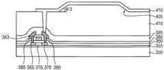
도 17을 참조하면, 게이트 절연막(215) 상에 액티브 패턴(230)과 소스 및 드레인 전극(220, 225)을 덮는 제1 보호막(235)을 형성한다. 제1 보호막(235)은 액티브 패턴(230)을 충분하게 커버하는 두께를 가질 수 있다. 제1 보호막(235)은 유기 물질, 무기 물질 등을 스핀 코팅 공정, 프린팅 공정, 스퍼터링 공정, 화학 기상 증착 공정, 원자층 적층 공정, 플라즈마 증대 화학 기상 증착 공정, 고밀도 플라즈마-화학 기상 증착 공정, 진공 증착 공정 등으로 게이트 절연막(215) 상에 도포하여 형성될 수 있다. 다른 예시적인 실시예들에 있어서, 후속하여 형성되는 절연층(245)의 구성 물질, 치수 등에 따라 제1 보호막(235)이 형성되지 않을 수도 있다.Referring to FIG. 17, a first
제1 보호막(235) 상에 절연층(245)을 형성한다. 절연층(245)은 2 이상의절연막들을 포함하는 다층 구조로 형성될 수 있다. 이 경우, 절연층(110)의 절연막들은 각기 도 1 및 도 2를 참조하여 설명한 제1 및 제2 절연막(5, 15)과 실질적으로 동일하거나 실질적으로 유사한 물질을 사용하여 형성될 수 있다. 또한, 절연층(245)의 절연막들은 각기 도 1 및 도 2를 참조하여 설명한 제1 및 제2 절연막(5, 15)과 실질적으로 동일하거나 실질적으로 유사한 공정들을 통해 제1 보호막(235) 상에 형성될 수 있다.An insulating
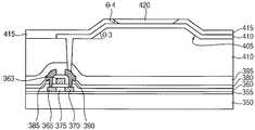
절연층(245)에 측벽이 제5 경사각(θ3)을 갖는 경사 구조(255)를 형성한다. 예시적인 실시예들에 있어서, 제1 보호막(235) 상에 제1 절연막(도시되지 않음)을 형성한 후, 상기 제1 절연막에 소정의 간격으로 이격되는 제1 리세스들(도시되지 않음)을 형성한다. 이 때, 인접하는 제1 리세스들 사이의 거리는 후속하여 형성되는 돌출된 형태의 경사 구조(255)의 폭과 실질적으로 동일하거나 실질적으로 유사하다. 상기 제1 절연막 상에 상기 제1 리세스들을 개재하여 제2 절연막을 형성한 다음, 상기 제1 리세스들 상부에 위치하는 상기 제2 절연막을 부분적으로 식각한다. 이에 따라, 상기 제2 절연막에는 상기 제1 리세스들에 연통되는 제2 리세스들이 형성된다. 다음에, 상기 제1 및 제2 절연막을 리플로우시킴으로써, 절연층(245)에 돌출되는 형태의 경사 구조(255)를 형성한다. 여기서, 경사 구조(255)는 상기 제1 및 제2 리세스들로부터 형성되는 인접하는 리세스들 사이에 위치한다. 예를 들면, 2개의 인접하는 리세스들 사이에 돌출되는 경사 구조(255)가 위치할 수 있다. 경사 구조(255)의 제5 경사각(θ3)은 인접하는 리세스들의 측벽 경사각과 실질적으로 동일하거나 실질적으로 유사하다. 예를 들면, 돌출된 형상의 경사 구조(255)는 제5 경사각(θ3)은 제1 기판(200)에 실질적으로 평행한 방향에 대하여 약 20°내지 약 70°정도가 될 수 있다.And an
다시 도 17을 참조하면, 절연층(245)과 제1 보호층(215)을 관통하여 드레인 전극(225)을 부분적으로 노출시키는 홀(250)이 형성된다. 이러한 홀(250)은 절연층(245)에 돌출된 경사 구조(255)를 형성하는 공정 동안 형성될 수 있지만, 절연층(245)에 돌출된 경사 구조(255)를 형성한 후에도 형성될 수도 있다.Referring again to FIG. 17, a
예시적인 실시예들에 있어서, 절연층(245)의 경사 구조(255) 측벽의 제5 경사각(θ3)은 도 4를 참조하여 설명한 경사 구조(25)의 측벽의 제3 경사각(θ1)과 실질적으로 동일하거나 실질적으로 유사할 수 있다. 절연층(245)의 경사 구조(255)가 도 17에 예시한 바와 같이 돌출된 형상을 가질 경우, 절연층(245)을 포함하는 상기 유기 발광 표시 장치는 배면 발광 방식을 가질 수 있다.The fifth inclination angle 3 of the side wall of the
도 18을 참조하면, 상술한 바와 같이 돌출된 형상의 경사 구조(255)를 갖는 절연층(245) 상에 홀(250)을 채우는 제1 전극(260)을 형성한다. 제1 전극(260)은 드레인 전극(225)에 접촉되며, 돌출된 경사 구조(255)의 양측벽들과 상면 상에 배치된다. 제1 전극(260)이 돌출된 경사 구조(255)를 커버하기 때문에, 제1 전극(260)의 양측부도 제5 경사각(θ3)과 실질적으로 동일하거나 실질적으로 유사한 경사각을 가질 수 있다. 예를 들면, 경사 구조(255)의 양측벽들 상에 위치하는 제1 전극(260)의 양측부의 경사각은 각기 약 20°내지 약 70°정도가 될 수 있다.Referring to FIG. 18, a
절연층(245)과 제1 전극(260) 상에는 상기 유기 발광 표시 장치의 발광 영역과 비발광 영역을 정의하는 화소 정의막(265)이 형성된다. 화소 정의막(265)은 유기 물질 또는 무기 물질을 사용하여 형성될 수 있다. 화소 정의막(265)은 상기 비발광 영역으로부터 상기 발광 영역에 위치하는 경사 구조(255)의 측벽들의 상부까지 연장될 수 있다. 즉, 화소 정의막(265)은 경사 구조(255)의 상면 상에는 위치하지 않는다. 경사 구조(255)의 측벽들 상에 위치하는 제1 전극(260) 상에도 화소 정의막(265)이 형성되기 때문에, 화소 정의막(265)의 측부들도 경사 구조(255)의 측벽들 상에서 제5 경사각(θ3)과 실질적으로 동일하거나 실질적으로 유사한 경사각을 가질 수 있다.A
화소 정의막(265)의 일부와 제1 전극(260) 상에는 유기 발광 구조물(270)이 형성된다. 유기 발광 구조물(270)은 유기 발광층을 포함하는 다층 구조를 가질 수 있다. 유기 발광 구조물(270)은 다양한 색광을 발생시킬 수 있는 발광 물질로 구성될 수 있지만, 이러한 발광 물질들이 적층된 구성을 가질 수도 있다.An organic
예시적인 실시예들에 있어서, 유기 발광 구조물(270)은 상기 발광 영역에만 배치될 수 있다. 예를 들면, 유기 발광 구조물(270)은 경사 구조(255)의 상면과 화소 정의막(265)의 일부 상에 형성될 수 있다. 따라서, 유기 발광 구조물(270)의 측부는 상대적으로 큰 경사각을 가질 수 있다. 예를 들면, 유기 발광 구조물(270)의 측벽은 제1 기판(200)에 실질적으로 수평한 축선에 대하여 약 40°내지 약 90°정도의 경사각을 가질 수 있다. 그 결과, 돌출된 경사 구조(255)의 측벽, 제1 전극(260)의 측부 및 화소 정의막(265)의 측부의 경사각들에 대한 유기 발광 구조물(270)의 측부의 경사각의 비율은 약 1.0: 0.2 내지 약 1.0: 1.8 정도가 될 수 있다.In the exemplary embodiments, the organic
도 19를 참조하면, 화소 정의막(265)과 유기 발광 구조물(270) 상에 제2 전극(275)을 형성한다. 상기 유기 발광 표시 장치가 배면 발광 방식을 가질 경우, 제2 전극(275)은 반사성을 갖는 물질을 사용하여 형성될 수 있다. 유기 발광 구조물(270)의 구조에 따라 제2 전극(275)은 화소 정의막(265)과 유기 발광 구조물(270) 상에 실질적으로 균일한 두께로 형성될 수 있다. 이 경우, 제2 전극(275) 중에서 돌출된 경사 구조(255)의 측벽에 인접하는 부분은 제5 경사각(θ3)과 실질적으로 동일하거나 실질적으로 유사한 경사각을 가질 수 있다.Referring to FIG. 19, a
제2 전극(275) 상에는 제2 보호막(280)이 형성된다. 제2 보호막(280)은 유기 물질, 무기 물질 등을 사용하여 형성될 수 있으며, 상기 발광 영역으로부터 상기 비발광 영역까지 연장될 수 있다. 제2 보호막(280) 상에는 투명 절연 기판인 제2 기판(290)이 배치된다. 이 경우, 상기 비발광 영역에서 제2 보호막(280)과 제2 기판(290) 사이에는 소정의 공간(285)이 제공될 수 있다. 이와 같은 공간(285)에는 공기 혹은 질소와 같은 불활성 기체 등이 채워질 수 있으며, 광 투과성과 흡습성을 갖는 수지가 충진될 수도 있다. 다른 예시적인 실시예들에 있어서, 추가적인 충진 물질의 존재에 따라 제2 전극(275)과 제2 기판(290) 사이에 제2 보호막(280)이 제공되지 않을 수도 있다.A
본 발명의 예시적인 실시예들에 따르면, 제1 전극(260), 화소 정의막(265) 및 제2 전극(275)의 측부들이 각기 돌출된 형상을 갖는 경사 구조(255) 인하여 유기 발광 구조물(270)로부터 발생되는 광의 전반사를 방지할 수 있는 원하는 경사각을 가지기 때문에, 상기 유기 발광 표시 장치의 광 효율을 크게 향상시킬 수 있다.According to exemplary embodiments of the present invention, since the sides of the
도 20 및 도 21은 본 발명의 또 다른 예시적인 실시예들에 따른 유기 발광 표시 장치의 제조 방법을 설명하기 위한 단면도들이다. 도 12 내지 도 13에 있어서, 절연층, 제1 전극, 유기 발광 구조물 등을 제외하면 도 5 내지 도 11을 참조하여 설명한 유기 발광 표시 장치와 실질적으로 동일하거나 실질적으로 유사한 구성을 가지는 유기 발광 표시 장치의 제조 방법을 예시적으로 설명하지만, 도 12 및 도 13에 도시한 제조 방법은 스위칭 소자, 보호층(들), 전극들, 유기 발광 구조물 등이 다양한 구조로 배치된 구성을 가지는 다른 유기 발광 표시 장치들에도 적용 가능함을 이해할 수 있을 것이다.20 and 21 are cross-sectional views illustrating a method of manufacturing an organic light emitting diode display according to still another exemplary embodiment of the present invention. 12 to 13, an organic light emitting display device having substantially the same or substantially similar structure as the organic light emitting display device described with reference to FIGS. 5 to 11, except for an insulating layer, a first electrode, However, the manufacturing method shown in FIGS. 12 and 13 is different from the organic light emitting display having the switching element, the protective layer (s), the electrodes, the organic light emitting structure, It will be appreciated that the invention is also applicable to devices.
도 20을 참조하면, 도 14 내지 도 17을 참조하여 설명한 공정들과 실질적으로 동일하거나 실질적으로 유사한 공정들을 수행하여, 제1 기판(200) 상에 스위칭 소자, 제1 보호막(235) 및 경사 구조(255)을 갖는 절연층(245)을 형성한다.Referring to FIG. 20, substantially similar or substantially similar processes as those described with reference to FIGS. 14 to 17 are performed to form a switching device, a first
도 20에 도시한 바와 같이, 절연층(245)에 도 12를 참조하여 설명한 공정들과 실질적으로 동일하거나 실질적으로 유사한 공정들을 수행함으로써, 돌출된 경사 구조(255)에 복수의 돌기(258)들을 형성한다. 따라서, 절연층(245)은 복수의 돌기(258)들을 포함하며, 절연층(245)에는 양측벽들이 각기 제5 경사각(θ3)을 가지는 경사 구조(255)가 제공된다.As shown in FIG. 20, by performing processes substantially the same or substantially similar to those described with reference to FIG. 12 in the insulating
제1 전극(300)은 절연층(245)과 제1 보호막(235)을 관통하는 홀을 채우며 절연층(245)과 경사 구조(245) 상에 형성된다. 제1 전극(300)의 측부들도 돌출된 경사 구조(245)의 양측벽들 상에서 각기 제5 경사각(θ3)과 실질적으로 동일하거나 실질적으로 유사한 경사각을 가진다. 또한, 제1 전극(300)에는 절연층(245)의 돌기(258)들에 기인하는 복수의 돌출부(303)들이 형성된다.The
제1 전극(300)과 절연층(245) 상에는 발광 영역과 비발광 영역을 정의하는 화소 정의막(265)이 형성된다. 화소 정의막(265)은 상기 비발광 영역으로부터 상기 발광 영역에 위치하는 경사 구조(255)의 양측벽들 상으로 연장될 수 있다. 돌출된 경사 구조(255)의 양측벽들 상에 위치하는 제1 전극(300) 상에도 화소 정의막(265)이 위치하기 때문에, 화소 정의막(265)의 측부들도 경사 구조(255)의 양측벽들 상에서 제5 경사각(θ3)과 실질적으로 동일하거나 실질적으로 유사한 경사각을 가진다.A
제1 전극(300)과 화소 정의막(265)의 일부 상에는 유기 발광 구조물(315)이 형성된다. 예시적인 실시예들에 있어서, 유기 발광 구조물(315)은 돌출된 경사 구조(255)의 상면과 화소 정의막(265)의 일부 상에만 형성된다. 따라서, 유기 발광 구조물(315)의 양측부들은 각기 상대적으로 큰 경사각을 가질 수 있다. 유기 발광 구조물(315)이 돌출부(303)들을 갖는 제1 전극(300) 상에 형성될 경우, 유기 발광 구조물(315)에는 돌출부(303)들에 대응하는 복수의 리세스들 또는 그루브들이 형성된다. 이와 같은 리세스들 또는 그루브들에 따라 유기 발광 구조물(315)은 복수의 부분들로 구분될 수도 있다.An organic
도 21을 참조하면, 화소 정의막(265)과 유기 발광 구조물(315) 상에 제2 전극(275)을 형성한다. 유기 발광 표시 장치가 배면 발광 방식을 가질 경우, 제2 전극(275)은 반사성을 갖는 물질을 포함할 수 있다. 제2 전극(275)은 유기 발광 구조물(315)의 프로파일을 따라 화소 정의막(265)과 유기 발광 구조물(315) 상에 균일한 두께로 형성될 수 있다. 또한, 경사 구조(255)의 측벽에 인접하는 제2 전극(275)의 일부는 제5 경사각(θ3)과 실질적으로 동일하거나 실질적으로 유사한 경사각을 가질 수 있다.Referring to FIG. 21, a
제2 전극(275) 상에는 제2 보호막(280)이 형성된다. 제2 보호막(280)은 상기 발광 영역 및 상기 비발광 영역에 배치될 수 있다. 제2 보호막(280) 상에는 제2 기판(290)이 배치된다. 이 때, 상기 비발광 영역에서 제2 보호막(280)과 제2 기판(290) 사이에는 소정의 공간(285)이 마련될 수 있다. 그러나, 추가적인 충진 물질의 존재에 따라 제2 전극(275)과 제2 기판(290) 사이에는 제2 보호막(280)이 형성되지 않을 수 있다.A
도 22 내지 도 24는 본 발명의 또 다른 예시적인 실시예들에 따른 유기 발광 표시 장치의 제조 방법을 설명하기 위한 단면도들이다. 도 22 내지 도 24에 있어서, 절연층, 제1 전극, 화소 정의막, 유기 발광 구조물 등을 제외하면 도 5 내지 도 11을 참조하여 설명한 유기 발광 표시 장치와 실질적으로 동일하거나 실질적으로 유사한 구성을 가지는 유기 발광 표시 장치의 제조 방법을 예시적으로 설명하지만, 도 22 내지 도 24에 도시한 제조 방법은 스위칭 소자, 보호막(들), 전극들, 절연층(들), 유기 발광 구조물 등이 다양한 구조로 배치된 구성을 가지는 다른 유기 발광 표시 장치들에도 적용 가능함을 이해할 수 있을 것이다.FIGS. 22 to 24 are cross-sectional views illustrating a method for manufacturing an organic light emitting display according to still another exemplary embodiment of the present invention. In FIGS. 22 to 24, except for the insulating layer, the first electrode, the pixel defining layer, the organic light emitting structure, and the like, substantially the same or substantially similar structure as the organic light emitting display device described with reference to FIGS. 5 to 11 Although the manufacturing method of the organic light emitting diode display device will be described by way of example, the manufacturing method shown in FIGS. 22 to 24 is not limited to the switching device, the protective film (s), the electrodes, the insulating layer It will be understood that the present invention is also applicable to other organic light emitting display devices having the arranged configuration.
도 22를 참조하면, 도 7 및 도 8을 참조하여 설명한 공정들과 실질적으로 동일하거나 실질적으로 유사한 공정들을 수행하여 제1 기판(350) 상에 버퍼층(355), 스위칭 소자, 제1 보호막(395) 등을 형성한다. 여기서, 상기 스위칭 소자는 반도체 패턴, 게이트 절연막(360), 게이트 전극(363), 층간 절연막(380), 소스 전극(385), 드레인 전극(390) 등을 포함한다. 상기 스위칭 소자의 반도체 패턴은 소스 영역(365), 드레인 영역(370) 및 채널 영역(375)으로 구분될 수 있다.Referring to FIG. 22, a
제1 보호막(395) 상에는 돌출된 경사 구조(405)를 포함하는 절연층(400)이 형성된다. 또한, 절연층(400)에는 드레인 전극(390)을 부분적으로 노출시키는 홀이 형성된다. 절연층(400)은 적어도 2 이상의 절연막들을 포함하는 다층 구조로 형성될 수 있다. 절연층(400)의 절연막들은 각기 도 1 및 도 2를 참조하여 설명한 제1 및 제2 절연막(5, 15)과 실질적으로 동일하거나 실질적으로 유사한 물질을 사용하여 형성될 수 있다. 또한, 절연층(400)의 절연막들은 각기 도 1 및 도 2를 참조하여 설명한 제1 및 제2 절연막(5, 15)과 실질적으로 동일하거나 실질적으로 유사한 공정들을 통해 제1 보호막(395) 상에 형성될 수 있다.An insulating layer 400 including a protruding
예시적인 실시예들에 따르면, 제1 보호막(395) 상에 제1 절연막(도시되지 않음)과 제2 절연막(도시되지 않음)을 형성한다. 여기서, 상기 제1 및 제2 절연막들은 각기 실질적으로 평탄한 상면을 가질 수 있다. 상기 제2 절연막에 소정의 간격으로 이격되는 제1 리세스들(도시되지 않음)을 형성한다. 이 경우, 인접하는 제1 리세스들 사이의 거리는 후속하여 형성되는 돌출된 형태의 경사 구조(405)의 폭과 실질적으로 동일하거나 실질적으로 유사하다. 상기 제2 절연막 상에 상기 제1 리세스들을 개재하여 제3 절연막을 형성한 후, 상기 제1 리세스들 상부에 위치하는 상기 제3 절연막을 부분적으로 제거한다. 따라서, 상기 제3 절연막에는 상기 제1 리세스들에 연통되는 제2 리세스들이 형성된다. 이후에, 상기 제2 및 제3 절연막을 리플로우시켜, 절연층(400)에 돌출된 형상의 경사 구조(405)를 형성한다. 돌출된 경사 구조(405)는 인접하는 제1 리세스들 사이 또는 인접하는 제2 리세스들 사이에 형성된다. 절연층(400)의 경사 구조(405)가 돌출된 형상을 가질 경우, 이러한 경사 구조(405)를 포함하는 상기 유기 발광 표시 장치는 배면 발광 방식을 가질 수 있다. 경사 구조(405)의 제5 경사각(θ3)은 인접하는 리세스들의 측벽 경사각과 실질적으로 동일하거나 실질적으로 유사하다. 예를 들면, 돌출된 경사 구조(405)의 측벽은 제1 기판(350)에 실질적으로 평행한 방향에 대하여 약 20°내지 약 70°정도의 제5 경사각(θ3)을 가질 수 있다.According to exemplary embodiments, a first insulating film (not shown) and a second insulating film (not shown) are formed on the first
돌출된 경사 구조(405)를 갖는 절연층(400) 상에 드레인 전극(390)을 부분적으로 노출시키는 홀을 채우면서 제1 전극(410)을 형성한다. 예시적인 실시예들에 있어서, 상기 홀을 채우면서 절연층(400) 상에 경사 구조(405)를 커버하는 제1 전극층(도시되지 않음)을 형성한다. 상기 제1 전극층 상에 식각 마스크(도시되지 않음)를 형성한 후, 상기 식각 마스크를 이용하여 상기 제1 전극층을 패터닝함으로써, 인접하는 화소 영역들에서 서로 분리되는 제1 전극(410)들을 형성한다. 제1 전극(410)은 드레인 전극(390)에 접속되고, 절연층(400)의 돌출된 경사 구조(405)의 양측벽들과 상면 상에 배치된다. 제1 전극(410)이 돌출된 경사 구조(405) 상에 형성되기 때문에, 제1 전극(410)의 양측부도 제5 경사각(θ3)과 실질적으로 동일하거나 실질적으로 유사한 경사각을 가질 수 있다. 예를 들면, 제1 전극(410)의 양측부의 경사각은 각기 제1 기판(350)에 실질적으로 평행한 축선에 대하여 약 20°내지 약 70°정도가 될 수 있다.The
도 23을 참조하면, 절연층(400)과 제1 전극(410) 상에 화소 정의막(415)을 형성하여 상기 유기 발광 표시 장치의 발광 영역과 비발광 영역을 정의한다. 화소 정의막(415)은 유기 물질 또는 무기 물질을 사용하여 형성될 수 있다. 화소 정의막(415)은 상기 비발광 영역으로부터 상기 발광 영역에 위치하는 경사 구조(405)의 상부까지 연장될 수 있다.Referring to FIG. 23, a
예시적인 실시예들에 있어서, 화소 정의막(415)은 상기 발광 영역에서 제1 전극(410)을 커버하도록 연장될 수 있다. 이 경우, 화소 정의막(415)에는 경사 구조(405)의 상면 상에 위치하는 제1 전극(410)을 노출시키는 개구가 형성된다. 화소 정의막(415)의 개구의 측벽은 상기 제5 경사각(θ3)과 다른 제6 경사각(θ4)을 가질 수 있다. 예를 들면, 화소 정의막(415)의 개구의 측벽의 제6 경사각(θ4)은 제1 기판(350)에 실질적으로 평행한 방향에 대하여 약 110°내지 약 160°정도가 될 수 있다. 화소 정의막(415)의 개구에 의해 상기 유기 발광 표시 장치의 발광 영역이 정의될 수 있다. 한편, 경사 구조(405)의 측벽들 상부에 위치하는 화소 정의막(415)의 측부들은 경사 구조(405)의 측벽들 상에서 제5 경사각(θ3)과 실질적으로 동일하거나 실질적으로 유사한 경사각을 가질 수 있다.In the exemplary embodiments, the
유기 발광 구조물(420)은 화소 정의막(415)의 개구 내에서 제1 전극(410) 상에 형성된다. 예시적인 실시예들에 따르면, 유기 발광 구조물(420)은 화소 정의막(415)의 개구 내에 매립될 수 있다. 즉, 유기 발광 구조물(420)은 화소 정의막(415)의 개구를 완전히 채우면서 실질적으로 평탄한 상면을 가질 수 있다. 따라서, 유기 발광 구조물(420)의 측벽도 화소 정의막(415)의 개구의 제6 경사각(θ4)과 실질적으로 동일하거나 실질적으로 유사한 경사각을 가질 수 있다. 예를 들면, 유기 발광 구조물(420)의 측벽은 제1 기판(350)에 실질적으로 평행한 축선에 대하여 약 110°내지 약 160°정도의 경사각을 가질 수 있다. 이에 따라, 돌출된 경사 구조(405)의 측벽, 제1 전극(410)의 측부 및 화소 정의막(415)의 측부의 경사각들에 대한 유기 발광 구조물(420)의 측부의 경사각의 비율은 약 1.0: 1.6 내지 약 1.0: 8.0 정도로 상대적으로 커질 수 있다. 유기 발광 구조물(420)은 각 화소마다 유기 발광층을 포함하는 다층 구조를 가질 수 있다. 유기 발광 구조물(420)은 화소들에 따라 다양한 색광을 발생시킬 수 있는 발광 물질을 포함할 수 있지만, 이러한 다양한 발광 물질들이 적층되어 백색광을 발생시키는 구성을 가질 수도 있다.The organic
도 24를 참조하면, 화소 정의막(415)과 유기 발광 구조물(420) 상에 제2 전극(425)을 형성한다. 상기 유기 발광 표시 장치가 배면 발광 방식을 가질 경우, 제2 전극(425)은 반사성을 갖는 물질을 사용하여 형성될 수 있다. 제2 전극(425)은 화소 정의막(415)과 유기 발광 구조물(420) 상에 실질적으로 균일한 두께로 형성될 수 있다. 여기서, 제2 전극(425) 중에서 돌출된 경사 구조(405)의 측벽에 인접하는 부분은 제5 경사각(θ3)과 실질적으로 동일하거나 실질적으로 유사한 경사각을 가질 수 있다.Referring to FIG. 24, a
제2 전극(425) 상에는 제2 보호막(430)이 형성된다. 제2 보호막(430)은 유기 물질, 무기 물질 등을 사용하여 형성될 수 있으며, 상기 발광 영역으로부터 상기 비발광 영역까지 연장될 수 있다. 제2 보호막(430) 상에는 투명 절연 기판인 제2 기판(430)이 배치된다. 여기서, 상기 유기 발광 표시 장치의 비발광 영역에서 제2 보호막(430)과 제2 기판(450) 사이에는 소정의 공간(435)이 제공될 수 있다. 이러한 공간(435)에는 공기 또는 질소와 같은 불활성 기체 등이 충진될 수 있지만, 경우에 따라 광 투과성과 흡습성을 갖는 수지가 채워질 수도 있다. 다른 예시적인 실시예들에 따르면, 추가적인 충진 물질의 존재에 따라 제2 전극(425)과 제2 기판(450) 사이에는 제2 보호막(430)이 형성되지 않을 수도 있다.A second
본 발명의 예시적인 실시예들에 따르면, 제1 전극(410), 화소 정의막(415) 및 제2 전극(425)의 측부들이 각기 돌출된 형상을 갖는 경사 구조(405) 인하여 유기 발광 구조물(420)로부터 발생되는 광의 전반사를 방지할 수 있는 원하는 경사각을 가지기 때문에, 상기 유기 발광 표시 장치의 광 효율을 크게 향상시킬 수 있다. 특히, 유기 발광 구조물(420)이 화소 정의막(415)의 개구에 매립될 수 있으므로, 유기 발광 구조물(420)로부터 발생되어 상기 비발광 영역으로 진행되는 광을 돌출된 경사 구조(405) 상부에 위치하는 제2 전극(425)에 의해 다시 상기 발광 영역으로 반사시킬 수 있다.According to the exemplary embodiments of the present invention, since the sides of the
본 발명의 예시적인 실시예들에 있어서, 경사 구조를 갖는 절연층을 구비하는 유기 발광 표시 장치는 광학적 공진을 요구하지 않는 간단한 구성을 가지면서도 종래의 유기 발광 표시 장치에 비하여 크게 향상된 광 효율을 가지기 때문에 상기 유기 발광 표시 장치가 나타내는 영상의 휘도, 콘트라스트, 측면 시인성 등을 개선시킬 수 있다.In the exemplary embodiments of the present invention, an OLED display device having an insulating layer having a tilted structure has a significantly improved light efficiency compared to a conventional organic light emitting display device while having a simple structure that does not require optical resonance Therefore, the brightness, contrast, side visibility, etc. of the image represented by the organic light emitting display device can be improved.
5: 제1 절연막 10: 제1 리세스
15: 제2 절연막 20: 제2 리세스
25, 120, 255, 405: 경사 구조 30, 110, 245, 400: 절연층
50, 200, 350: 제1 기판 55, 205, 355: 버퍼층
60: 반도체 패턴 65, 215, 360: 게이트 절연막
70, 210, 363: 게이트 전극 75, 365: 소스 영역
80, 370: 드레인 영역 85, 375: 채널 영역
90, 380: 층간 절연막 95, 220, 385: 소스 전극
100, 225, 390: 드레인 전극 105, 235, 395: 제1 보호막
125, 133, 260, 300, 410: 제1 전극
128, 258: 절연층의 돌기 134, 303: 제1 전극의 돌출부
130, 265, 415: 화소 정의막
135, 155, 270, 315: 유기 발광 구조물
140, 275, 425: 제2 전극 145, 280, 430: 제2 보호막
150, 290, 450: 제2 기판 230: 액티브 패턴5: first insulating film 10: first recess
15: second insulating film 20: second recess
25, 120, 255, 405:
50, 200, 350:
60:
70, 210, 363:
80, 370: drain
90, 380:
100, 225, 390:
125, 133, 260, 300, 410:
128, 258:
130, 265, 415: pixel defining film
135, 155, 270, 315: organic light emitting structure
140, 275, 425: a
150, 290, 450: second substrate 230: active pattern
Claims (27)
Translated fromKorean상기 제1 기판 상에 배치되며, 경사 구조를 구비하는 절연층;
상기 절연층 상에 배치되는 제1 전극;
상기 절연층 및 상기 제1 전극 상에 배치되며, 발광 영역과 비발광 영역을 정의하는 화소 정의막;
상기 발광 영역의 상기 제1 전극 상에 배치되는 유기 발광 구조물;
상기 화소 정의막 및 상기 유기 발광 구조물 상에 배치되는 제2 전극; 및
상기 제2 전극 상에 배치되는 제2 기판을 포함하며,
상기 경사 구조는 상기 절연층의 두께보다 작은 깊이로 상기 절연층의 일부에 배치되고,
상기 경사 구조의 측벽과 상기 유기 발광 구조물의 측부는 동일한 경사각을 가지는 것을 특징으로 하는 유기 발광 표시 장치.A first substrate;
An insulating layer disposed on the first substrate and having an inclined structure;
A first electrode disposed on the insulating layer;
A pixel defining layer disposed on the insulating layer and the first electrode, the pixel defining layer defining a light emitting region and a non-emitting region;
An organic light emitting structure disposed on the first electrode of the light emitting region;
A second electrode disposed on the pixel defining layer and the organic light emitting structure; And
And a second substrate disposed on the second electrode,
Wherein the inclined structure is disposed in a part of the insulating layer at a depth smaller than the thickness of the insulating layer,
Wherein the side wall of the tilted structure and the side of the organic light emitting structure have the same inclination angle.
Priority Applications (4)
| Application Number | Priority Date | Filing Date | Title |
|---|---|---|---|
| US13/530,057US9029838B2 (en) | 2011-06-29 | 2012-06-21 | Methods of forming inclined structures on insulation layers, organic light emitting display devices and methods of manufacturing organic light emitting display devices |
| TW101123214ATWI565049B (en) | 2011-06-29 | 2012-06-28 | Methods of forming inclined structures on insulation layers, organic light emitting display devices with the inclined structures and methods of manufacturing the organic light emitting display devices |
| CN201210223710.1ACN103000823B (en) | 2011-06-29 | 2012-06-29 | Method for forming inclined structure, organic light-emitting display device and manufacturing method thereof |
| CN201610052044.8ACN105514144B (en) | 2011-06-29 | 2012-06-29 | Organic Light Emitting Display Device |
Applications Claiming Priority (2)
| Application Number | Priority Date | Filing Date | Title |
|---|---|---|---|
| KR1020110063558 | 2011-06-29 | ||
| KR20110063558 | 2011-06-29 |
Publications (2)
| Publication Number | Publication Date |
|---|---|
| KR20130007421A KR20130007421A (en) | 2013-01-18 |
| KR101881133B1true KR101881133B1 (en) | 2018-07-24 |
Family
ID=47837971
Family Applications (1)
| Application Number | Title | Priority Date | Filing Date |
|---|---|---|---|
| KR1020120059068AActiveKR101881133B1 (en) | 2011-06-29 | 2012-06-01 | Method of forming an inclided structure in an insulation layer, organic light emitting device and method of manufcaturing an organic light emitting device |
Country Status (3)
| Country | Link |
|---|---|
| KR (1) | KR101881133B1 (en) |
| CN (2) | CN103000823B (en) |
| TW (1) | TWI565049B (en) |
Cited By (1)
| Publication number | Priority date | Publication date | Assignee | Title |
|---|---|---|---|---|
| US11751435B2 (en) | 2020-12-02 | 2023-09-05 | Samsung Display Co., Ltd. | Display device and method of manufacturing the display device |
Families Citing this family (52)
| Publication number | Priority date | Publication date | Assignee | Title |
|---|---|---|---|---|
| KR101900954B1 (en) | 2012-01-19 | 2018-09-21 | 삼성디스플레이 주식회사 | Organic light emitting device and manufacturing method thereof |
| KR102021027B1 (en) | 2013-02-28 | 2019-09-16 | 삼성디스플레이 주식회사 | Organic luminescence emitting display device |
| KR102028680B1 (en) | 2013-03-20 | 2019-11-05 | 삼성디스플레이 주식회사 | Organic light emitting diode display |
| JP2014220121A (en) | 2013-05-08 | 2014-11-20 | 株式会社ジャパンディスプレイ | Display device |
| KR102132884B1 (en)* | 2013-05-21 | 2020-07-13 | 삼성디스플레이 주식회사 | Organic light emitting display apparatus and manufacturing method of the same |
| US20140353622A1 (en)* | 2013-05-30 | 2014-12-04 | Samsung Display Co., Ltd. | Organic light-emitting display apparatus and method of manufacturing the same |
| KR102090709B1 (en) | 2013-05-31 | 2020-03-19 | 삼성디스플레이 주식회사 | White organic light emitting display device |
| KR102036328B1 (en)* | 2013-06-07 | 2019-10-25 | 삼성디스플레이 주식회사 | Organic luminescence emitting display device and method for manufacturing the same |
| KR102146070B1 (en)* | 2013-07-01 | 2020-08-21 | 삼성디스플레이 주식회사 | Organic Light Emitting Display |
| JP2015050011A (en) | 2013-08-30 | 2015-03-16 | 株式会社ジャパンディスプレイ | Electroluminescence device and method for manufacturing the same |
| CN104733632B (en)* | 2013-12-18 | 2017-06-06 | 昆山国显光电有限公司 | Organic light-emitting display device and its manufacture method |
| CN104103673B (en)* | 2014-07-09 | 2017-06-20 | 京东方科技集团股份有限公司 | A kind of OLED display and preparation method thereof |
| CN104538455A (en)* | 2014-12-31 | 2015-04-22 | 上海天马有机发光显示技术有限公司 | Method for manufacturing lightly-doped drain region, thin film transistor and array substrate |
| KR101664007B1 (en)* | 2014-12-31 | 2016-10-11 | 엘지디스플레이 주식회사 | Organic light emitting device and manufacturing method thereof |
| KR102626853B1 (en)* | 2015-10-30 | 2024-01-18 | 삼성디스플레이 주식회사 | Organic light emitting diode display |
| CN106910762B (en)* | 2015-12-23 | 2019-11-08 | 宸鸿光电科技股份有限公司 | Organic light emitting diode display device |
| CN105633304B (en)* | 2016-03-23 | 2018-03-06 | 深圳市华星光电技术有限公司 | The method for packing of oled substrate and OLED encapsulating structures |
| KR102608419B1 (en)* | 2016-07-12 | 2023-12-01 | 삼성디스플레이 주식회사 | Display Apparatus and Method for manufacturing the same |
| KR102572081B1 (en)* | 2016-07-29 | 2023-08-28 | 엘지디스플레이 주식회사 | Organic light emitting display device |
| KR102387859B1 (en) | 2016-09-30 | 2022-04-15 | 엘지디스플레이 주식회사 | Organic light emitting display device and method of manufacturing the same |
| KR102615687B1 (en)* | 2016-11-15 | 2023-12-21 | 삼성디스플레이 주식회사 | Display device |
| CN107068717A (en)* | 2017-04-06 | 2017-08-18 | 惠科股份有限公司 | Display panel and method for manufacturing the same |
| CN107154419A (en)* | 2017-04-06 | 2017-09-12 | 惠科股份有限公司 | Display panel and method for manufacturing the same |
| CN106992203B (en)* | 2017-04-24 | 2020-03-27 | 京东方科技集团股份有限公司 | Light-emitting structure, display panel and display device |
| CN107863449A (en) | 2017-10-26 | 2018-03-30 | 京东方科技集团股份有限公司 | A kind of organic electroluminescence device, its preparation method and display device |
| KR102444315B1 (en)* | 2017-12-29 | 2022-09-16 | 엘지디스플레이 주식회사 | Organic Light-Emitting Display apparatus having a light-emitting device |
| KR102560050B1 (en)* | 2018-03-16 | 2023-07-26 | 삼성디스플레이 주식회사 | Display device and method of manufacturing the same |
| CN108767136B (en) | 2018-06-05 | 2020-06-30 | 京东方科技集团股份有限公司 | A kind of mirror display screen and preparation method |
| CN108807556B (en)* | 2018-06-11 | 2021-01-29 | 京东方科技集团股份有限公司 | An optical sensor device and its manufacturing method, a display device, and a display device |
| CN109979983B (en) | 2018-06-22 | 2021-05-28 | 友达光电股份有限公司 | Organic Light Emitting Diode Display Device |
| CN108922867A (en)* | 2018-06-25 | 2018-11-30 | 武汉华星光电半导体显示技术有限公司 | Display panel and preparation method thereof |
| CN109378328B (en)* | 2018-09-28 | 2021-07-09 | 广州国显科技有限公司 | OLED display panel and OLED display device |
| CN109659338A (en)* | 2018-12-10 | 2019-04-19 | 武汉华星光电半导体显示技术有限公司 | OLED display |
| KR102075728B1 (en) | 2018-12-17 | 2020-02-10 | 엘지디스플레이 주식회사 | Display panel |
| KR102075741B1 (en) | 2018-12-17 | 2020-02-10 | 엘지디스플레이 주식회사 | Display panel |
| CN109860416B (en)* | 2019-01-09 | 2022-03-25 | 昆山工研院新型平板显示技术中心有限公司 | Pixel structure and OLED display panel with same |
| CN109873089B (en)* | 2019-02-28 | 2021-09-03 | 合肥鑫晟光电科技有限公司 | Light emitting diode display panel and manufacturing method thereof |
| CN109950282B (en) | 2019-03-25 | 2021-04-13 | 京东方科技集团股份有限公司 | Pixel structure, array substrate and display device |
| CN111969121B (en)* | 2019-05-20 | 2024-06-25 | 乐金显示有限公司 | Light-emitting display device |
| KR102730932B1 (en)* | 2019-06-19 | 2024-11-19 | 삼성디스플레이 주식회사 | Display device |
| CN110212012B (en)* | 2019-07-12 | 2022-02-25 | 昆山国显光电有限公司 | Display panel and display device |
| CN110459570B (en)* | 2019-08-19 | 2022-07-22 | 京东方科技集团股份有限公司 | An organic electroluminescence substrate and an organic electroluminescence display panel |
| US11444139B2 (en) | 2019-08-28 | 2022-09-13 | Wuhan China Star Optoelectronics Semiconductor Display Technology Co., Ltd. | Display panel providing planarization layer on pixel defining layer around light emitting functional layer, display device, and manufacturing method of the display panel |
| CN110600513B (en)* | 2019-08-28 | 2021-01-15 | 武汉华星光电半导体显示技术有限公司 | Display panel, display device and manufacturing method of display panel |
| US11237659B2 (en) | 2019-11-05 | 2022-02-01 | Lg Display Co., Ltd. | Touch display device |
| CN119584803A (en)* | 2019-11-06 | 2025-03-07 | 乐金显示有限公司 | Display Panel |
| CN111370590A (en)* | 2020-03-12 | 2020-07-03 | 深圳市华星光电半导体显示技术有限公司 | Display panel, preparation method thereof and display device |
| CN111223909A (en)* | 2020-03-18 | 2020-06-02 | 深圳市华星光电半导体显示技术有限公司 | Display panel and method of making the same |
| CN111769211B (en)* | 2020-07-01 | 2023-06-16 | 视涯科技股份有限公司 | A kind of organic light-emitting display panel and display device |
| CN113571559A (en)* | 2021-07-15 | 2021-10-29 | 深圳市华星光电半导体显示技术有限公司 | Display panel, preparation method thereof and display device |
| CN113707831B (en)* | 2021-08-30 | 2023-09-01 | 合肥鑫晟光电科技有限公司 | Display substrate, manufacturing method thereof, and display panel |
| US20250098498A1 (en)* | 2022-04-27 | 2025-03-20 | Chengdu Boe Optoelectronics Technology Co., Ltd. | Display apparatus and display panel |
Citations (3)
| Publication number | Priority date | Publication date | Assignee | Title |
|---|---|---|---|---|
| JP2008077953A (en) | 2006-09-21 | 2008-04-03 | Hitachi Displays Ltd | Organic EL display device |
| KR100934480B1 (en) | 2009-03-17 | 2009-12-30 | 실리콘 디스플레이 (주) | Organic light emitting display panel and manufacturing method thereof |
| JP2010097956A (en) | 2008-03-13 | 2010-04-30 | Panasonic Corp | Organic el display panel and method of manufacturing the same |
Family Cites Families (9)
| Publication number | Priority date | Publication date | Assignee | Title |
|---|---|---|---|---|
| JP2003257662A (en)* | 2002-03-04 | 2003-09-12 | Sanyo Electric Co Ltd | Electroluminescence display device and method of manufacturing the same |
| KR100552962B1 (en)* | 2003-08-28 | 2006-02-15 | 삼성에스디아이 주식회사 | Organic electroluminescent display and manufacturing method thereof |
| JP4815761B2 (en)* | 2003-11-27 | 2011-11-16 | セイコーエプソン株式会社 | Electro-optical device, method of manufacturing electro-optical device, and electronic apparatus |
| JP4534054B2 (en)* | 2004-06-25 | 2010-09-01 | 京セラ株式会社 | Organic EL display panel and its manufacturing method |
| JP4918752B2 (en)* | 2005-04-08 | 2012-04-18 | セイコーエプソン株式会社 | ORGANIC ELECTROLUMINESCENT DEVICE MANUFACTURING METHOD, ORGANIC ELECTROLUMINESCENT DEVICE, ELECTRONIC DEVICE |
| KR101326135B1 (en)* | 2006-11-27 | 2013-11-07 | 삼성디스플레이 주식회사 | Organic light emitting display and manufacturing method thereof |
| JP4485559B2 (en)* | 2007-09-26 | 2010-06-23 | 株式会社 日立ディスプレイズ | Liquid crystal display |
| KR100943948B1 (en)* | 2008-01-08 | 2010-02-26 | 삼성모바일디스플레이주식회사 | Display device |
| KR20100001597A (en)* | 2008-06-27 | 2010-01-06 | 삼성전자주식회사 | Display device and manufacturing method thereof |
- 2012
- 2012-06-01KRKR1020120059068Apatent/KR101881133B1/enactiveActive
- 2012-06-28TWTW101123214Apatent/TWI565049B/enactive
- 2012-06-29CNCN201210223710.1Apatent/CN103000823B/enactiveActive
- 2012-06-29CNCN201610052044.8Apatent/CN105514144B/enactiveActive
Patent Citations (3)
| Publication number | Priority date | Publication date | Assignee | Title |
|---|---|---|---|---|
| JP2008077953A (en) | 2006-09-21 | 2008-04-03 | Hitachi Displays Ltd | Organic EL display device |
| JP2010097956A (en) | 2008-03-13 | 2010-04-30 | Panasonic Corp | Organic el display panel and method of manufacturing the same |
| KR100934480B1 (en) | 2009-03-17 | 2009-12-30 | 실리콘 디스플레이 (주) | Organic light emitting display panel and manufacturing method thereof |
Cited By (2)
| Publication number | Priority date | Publication date | Assignee | Title |
|---|---|---|---|---|
| US11751435B2 (en) | 2020-12-02 | 2023-09-05 | Samsung Display Co., Ltd. | Display device and method of manufacturing the display device |
| US12185593B2 (en) | 2020-12-02 | 2024-12-31 | Samsung Display Co., Ltd. | Display device and method of manufacturing the display device |
Also Published As
| Publication number | Publication date |
|---|---|
| KR20130007421A (en) | 2013-01-18 |
| CN105514144B (en) | 2019-06-11 |
| CN103000823A (en) | 2013-03-27 |
| CN105514144A (en) | 2016-04-20 |
| TW201306249A (en) | 2013-02-01 |
| TWI565049B (en) | 2017-01-01 |
| CN103000823B (en) | 2016-08-03 |
Similar Documents
| Publication | Publication Date | Title |
|---|---|---|
| KR101881133B1 (en) | Method of forming an inclided structure in an insulation layer, organic light emitting device and method of manufcaturing an organic light emitting device | |
| US9029838B2 (en) | Methods of forming inclined structures on insulation layers, organic light emitting display devices and methods of manufacturing organic light emitting display devices | |
| KR101821167B1 (en) | Organic light emitting display device having a reflection structure and method of manufacturing an organic light emitting display device having a reflection structure | |
| KR101893376B1 (en) | Organic light emitting display device and method of manufacturing an organic light emitting display device | |
| US10454072B2 (en) | Organic light emitting display panel | |
| US10192947B2 (en) | Organic light emitting display panel and method of manufacturing the same | |
| KR102337348B1 (en) | Transparent organic light emitting display apparatus and method of manufacturing the same | |
| KR101941661B1 (en) | Organic light emitting diode device and manufacturing method thereof | |
| KR102447451B1 (en) | organic light emitting diode display | |
| TWI557896B (en) | Organic light emitting diode display and manufacturing method thereof | |
| KR101928582B1 (en) | Organic light emitting diode device and manufacturing method thereof | |
| KR101972169B1 (en) | Organic light emitting display device and manufacturing method thereof | |
| KR20170055587A (en) | Organic light emitting display device | |
| KR102099702B1 (en) | Organic light emitting display device and method of manufacturing having the same | |
| KR20140014682A (en) | Organic light emitting diode device and manufacturing method thereof | |
| KR20160034461A (en) | Organic light emitting display device and method of manufacturing an organic light emitting display device | |
| KR20160106793A (en) | Transparent organic light emitting display apparatus and method of manufacturing the same | |
| US10224511B2 (en) | Organic light emitting display device | |
| KR102075787B1 (en) | Organic light emitting display device and manufacturing method thereof |
Legal Events
| Date | Code | Title | Description |
|---|---|---|---|
| PA0109 | Patent application | Patent event code:PA01091R01D Comment text:Patent Application Patent event date:20120601 | |
| N231 | Notification of change of applicant | ||
| PN2301 | Change of applicant | Patent event date:20120730 Comment text:Notification of Change of Applicant Patent event code:PN23011R01D | |
| PG1501 | Laying open of application | ||
| A201 | Request for examination | ||
| PA0201 | Request for examination | Patent event code:PA02012R01D Patent event date:20170529 Comment text:Request for Examination of Application Patent event code:PA02011R01I Patent event date:20120601 Comment text:Patent Application | |
| E902 | Notification of reason for refusal | ||
| PE0902 | Notice of grounds for rejection | Comment text:Notification of reason for refusal Patent event date:20171023 Patent event code:PE09021S01D | |
| E701 | Decision to grant or registration of patent right | ||
| PE0701 | Decision of registration | Patent event code:PE07011S01D Comment text:Decision to Grant Registration Patent event date:20180430 | |
| GRNT | Written decision to grant | ||
| PR0701 | Registration of establishment | Comment text:Registration of Establishment Patent event date:20180717 Patent event code:PR07011E01D | |
| PR1002 | Payment of registration fee | Payment date:20180718 End annual number:3 Start annual number:1 | |
| PG1601 | Publication of registration | ||
| PR1001 | Payment of annual fee | Payment date:20210701 Start annual number:4 End annual number:4 | |
| PR1001 | Payment of annual fee | Payment date:20220620 Start annual number:5 End annual number:5 | |
| PR1001 | Payment of annual fee | Payment date:20240625 Start annual number:7 End annual number:7 |