KR101880723B1 - Organic light emitting display apparatus - Google Patents
Organic light emitting display apparatusDownload PDFInfo
- Publication number
- KR101880723B1 KR101880723B1KR1020110132126AKR20110132126AKR101880723B1KR 101880723 B1KR101880723 B1KR 101880723B1KR 1020110132126 AKR1020110132126 AKR 1020110132126AKR 20110132126 AKR20110132126 AKR 20110132126AKR 101880723 B1KR101880723 B1KR 101880723B1
- Authority
- KR
- South Korea
- Prior art keywords
- electrode
- layer
- light
- intermediate layer
- sub
- Prior art date
- Legal status (The legal status is an assumption and is not a legal conclusion. Google has not performed a legal analysis and makes no representation as to the accuracy of the status listed.)
- Active
Links
Images


Classifications
- H—ELECTRICITY
- H10—SEMICONDUCTOR DEVICES; ELECTRIC SOLID-STATE DEVICES NOT OTHERWISE PROVIDED FOR
- H10K—ORGANIC ELECTRIC SOLID-STATE DEVICES
- H10K59/00—Integrated devices, or assemblies of multiple devices, comprising at least one organic light-emitting element covered by group H10K50/00
- H10K59/80—Constructional details
- H10K59/875—Arrangements for extracting light from the devices
- H10K59/876—Arrangements for extracting light from the devices comprising a resonant cavity structure, e.g. Bragg reflector pair
- H—ELECTRICITY
- H10—SEMICONDUCTOR DEVICES; ELECTRIC SOLID-STATE DEVICES NOT OTHERWISE PROVIDED FOR
- H10K—ORGANIC ELECTRIC SOLID-STATE DEVICES
- H10K50/00—Organic light-emitting devices
- H10K50/80—Constructional details
- H10K50/85—Arrangements for extracting light from the devices
- H10K50/852—Arrangements for extracting light from the devices comprising a resonant cavity structure, e.g. Bragg reflector pair
- H—ELECTRICITY
- H10—SEMICONDUCTOR DEVICES; ELECTRIC SOLID-STATE DEVICES NOT OTHERWISE PROVIDED FOR
- H10K—ORGANIC ELECTRIC SOLID-STATE DEVICES
- H10K59/00—Integrated devices, or assemblies of multiple devices, comprising at least one organic light-emitting element covered by group H10K50/00
- H10K59/10—OLED displays
- H10K59/12—Active-matrix OLED [AMOLED] displays
- H10K59/121—Active-matrix OLED [AMOLED] displays characterised by the geometry or disposition of pixel elements
- H10K59/1213—Active-matrix OLED [AMOLED] displays characterised by the geometry or disposition of pixel elements the pixel elements being TFTs
- H—ELECTRICITY
- H10—SEMICONDUCTOR DEVICES; ELECTRIC SOLID-STATE DEVICES NOT OTHERWISE PROVIDED FOR
- H10K—ORGANIC ELECTRIC SOLID-STATE DEVICES
- H10K59/00—Integrated devices, or assemblies of multiple devices, comprising at least one organic light-emitting element covered by group H10K50/00
- H10K59/30—Devices specially adapted for multicolour light emission
- H10K59/35—Devices specially adapted for multicolour light emission comprising red-green-blue [RGB] subpixels
- H—ELECTRICITY
- H10—SEMICONDUCTOR DEVICES; ELECTRIC SOLID-STATE DEVICES NOT OTHERWISE PROVIDED FOR
- H10K—ORGANIC ELECTRIC SOLID-STATE DEVICES
- H10K59/00—Integrated devices, or assemblies of multiple devices, comprising at least one organic light-emitting element covered by group H10K50/00
- H10K59/80—Constructional details
- H10K59/875—Arrangements for extracting light from the devices
- H10K59/878—Arrangements for extracting light from the devices comprising reflective means
- H—ELECTRICITY
- H10—SEMICONDUCTOR DEVICES; ELECTRIC SOLID-STATE DEVICES NOT OTHERWISE PROVIDED FOR
- H10K—ORGANIC ELECTRIC SOLID-STATE DEVICES
- H10K2102/00—Constructional details relating to the organic devices covered by this subclass
- H10K2102/10—Transparent electrodes, e.g. using graphene
- H10K2102/101—Transparent electrodes, e.g. using graphene comprising transparent conductive oxides [TCO]
- H—ELECTRICITY
- H10—SEMICONDUCTOR DEVICES; ELECTRIC SOLID-STATE DEVICES NOT OTHERWISE PROVIDED FOR
- H10K—ORGANIC ELECTRIC SOLID-STATE DEVICES
- H10K2102/00—Constructional details relating to the organic devices covered by this subclass
- H10K2102/20—Metallic electrodes, e.g. using a stack of layers
- H—ELECTRICITY
- H10—SEMICONDUCTOR DEVICES; ELECTRIC SOLID-STATE DEVICES NOT OTHERWISE PROVIDED FOR
- H10K—ORGANIC ELECTRIC SOLID-STATE DEVICES
- H10K2102/00—Constructional details relating to the organic devices covered by this subclass
- H10K2102/301—Details of OLEDs
- H10K2102/351—Thickness
Landscapes
- Physics & Mathematics (AREA)
- Geometry (AREA)
- Engineering & Computer Science (AREA)
- Microelectronics & Electronic Packaging (AREA)
- Optics & Photonics (AREA)
- Electroluminescent Light Sources (AREA)
Abstract
Translated fromKoreanDescription
Translated fromKorean본 발명은 유기 발광 표시 장치에 관한 것으로 더 상세하게는 화질 특성을 을 향상하는 유기 발광 표시 장치에 관한 것이다.BACKGROUND OF THE INVENTION 1. Field of the Invention [0001] The present invention relates to an organic light emitting display, and more particularly, to an organic light emitting display that improves image quality.
근래에 표시 장치는 휴대가 가능한 박형의 평판 표시 장치로 대체되는 추세이다. 평판 표시 장치 중에서도 유기 발광 표시 장치는 자발광형 표시 장치로서 시야각이 넓고 콘트라스트가 우수할 뿐만 아니라 응답속도가 빠르다는 장점을 가져서 차세대 디스플레이 장치로 주목 받고 있다.In recent years, the display device has been replaced by a thin portable flat display device. Among the flat panel display devices, the organic light emitting display device is a self-luminous display device having a wide viewing angle, excellent contrast, and fast response speed, and has been attracting attention as a next generation display device.
유기 발광 표시 장치는 중간층, 제1 전극 및 제2 전극을 구비한다. 중간층은 유기 발광층을 구비하고, 제1 전극 및 제2 전극에 전압을 가하면 유기 발광층에서 가시광선을 발생하게 된다.The organic light emitting display includes an intermediate layer, a first electrode, and a second electrode. The intermediate layer includes an organic light emitting layer. When a voltage is applied to the first electrode and the second electrode, visible light is generated in the organic light emitting layer.
그러나 중간층에서 구현된 가시 광선의 특성을 사용자 측면에서 평가했을 때 최적의 상태로 제어하는 것이 용이하지 않다. 또한 중간층에서 발생한 가시 광선이 사용자에게 도달하기까지 가시 광선이 소멸되거나 변환된다. 결과적으로 유기 발광 표시 장치의 화질 특성을 향상하는데 한계가 있다.However, it is not easy to control the characteristics of visible light in the middle layer in the optimum state when the user side evaluates it. In addition, the visible light is lost or converted before visible light from the intermediate layer reaches the user. As a result, there is a limit in improving the image quality characteristic of the organic light emitting display device.
본 발명은 화질 특성을 향상하는 유기 발광 표시 장치를 제공할 수 있다.The present invention can provide an organic light emitting display device that improves image quality characteristics.
본 발명은 기판, 상기 기판 상에 형성된 제1 전극, 상기 제1 전극 상에 배치되는 제2 전극, 상기 제1 전극과 상기 제2 전극 사이에 배치되고 상기 제1 전극과 상기 제2 전극과 전기적으로 연결되고 유기 발광층을 구비하는 중간층 및 상기 중간층의 전체 영역 보다 작은 상기 중간층의 일 영역과 중첩되도록 형성된 광반사 부재를 포함하는 유기 발광 표시 장치를 개시한다.The present invention relates to a plasma display panel comprising a substrate, a first electrode formed on the substrate, a second electrode disposed on the first electrode, a second electrode disposed between the first electrode and the second electrode, And a light reflection member formed to overlap with one region of the intermediate layer which is smaller than the entire region of the intermediate layer and which is formed to overlap with an intermediate layer having an organic light emitting layer.
본 발명에 있어서 상기 광반사 부재는 가시 광선의 일부는 반사시키고 일부는 투과시킬 수 있다.In the present invention, the light reflection member can reflect part of visible light and transmit part of visible light.
본 발명에 있어서 상기 광반사 부재는 상기 중간층보다 작게 형성될 수 있다.In the present invention, the light reflection member may be formed to be smaller than the intermediate layer.
본 발명에 있어서 상기 광반사 부재는 상기 제1 전극보다 작게 형성 될 수 있다.In the present invention, the light reflection member may be formed to be smaller than the first electrode.
본 발명에 있어서 상기 기판과 상기 광반사 부재 사이에 배치된 제1 절연막을 더 포함할 수 있다.The organic light emitting display according to the present invention may further include a first insulating layer disposed between the substrate and the light reflecting member.
본 발명에 있어서 상기 기판과 상기 제1 절연막 사이에 배치된 버퍼층을 더 포함 할 수 있다.The buffer layer may further include a buffer layer disposed between the substrate and the first insulating layer.
본 발명에 있어서 상기 광반사 부재와 상기 제1 전극 사이에 배치된 제2 절연막을 더 포함 할 수 있다.The light reflection member may further include a second insulating film disposed between the light reflecting member and the first electrode.
본 발명에 있어서 상기 제2 절연막은 상기 제1 전극의 영역 중 상기 광반사 부재와 중첩되지 않는 영역과도 대응되도록 형성될 수 있다.In the present invention, the second insulating layer may be formed so as to correspond to a region of the first electrode that is not overlapped with the light reflecting member.
본 발명에 있어서 상기 제2 절연막과 상기 제1 전극 사이에 배치된 제3 절연막을 더 포함 할 수 있다.The organic electroluminescent device of the present invention may further include a third insulating film disposed between the second insulating film and the first electrode.
본 발명에 있어서 상기 광반사 부재는 Ag 또는 Al을 함유할 수 있다.In the present invention, the light reflection member may contain Ag or Al.
본 발명에 있어서 상기 제1 전극은 ITO, IZO, ZnO, In2O3, IGO 또는 AZO를 함유 할 수 있다.In the present invention, the first electrode may contain ITO, IZO, ZnO, In2O3, IGO or AZO.
본 발명에 있어서 상기 유기 발광 표시 장치는 복수의 부화소들을 구비하고, 상기 제1 전극, 중간층 및 상기 제2 전극은 상기 부화소들 각각에 대응되도록 형성되고, 상기 광반사 부재는 상기 복수의 부화소들 중 적어도 하나의 부화소들에 대응되도록 배치될 수 있다.The organic light emitting display according to the present invention may include a plurality of sub-pixels, wherein the first electrode, the intermediate layer, and the second electrode are formed to correspond to the sub-pixels, And may correspond to at least one of the pixels.
본 발명에 있어서 상기 복수의 부화소들은 서로 다른 종류의 색의 가시 광선을 구현하는 부화소들을 구비하고, 상기 광반사 부재는 상기 복수의 부화소들 중 어느 하나의 색의 가시 광선을 구현하는 부화소들에 대응되도록 배치될 수 있다.In the present invention, the plurality of sub-pixels may include sub-pixels for implementing visible light of different colors, and the light reflecting member may be a sub-pixel for embodying visible light of any one of the plurality of sub- So as to correspond to the cows.
본 발명에 있어서 상기 광반사 부재는 상기 복수의 부화소들 중 청색의 가시 광선을 구현하는 부화소들에 대응되도록 배치될 수 있다.In the present invention, the light reflection member may be arranged to correspond to the sub-pixels of the plurality of sub-pixels, which emit blue visible light.
본 발명에 있어서 상기 기판 상에 형성되고 상기 제1 전극과 전기적으로 연결되고, 활성층, 게이트 전극, 소스 전극 및 드레인 전극을 구비하는 박막 트랜지스터를 더 포함할 수 있다.The thin film transistor may further include a thin film transistor formed on the substrate and electrically connected to the first electrode, the thin film transistor including an active layer, a gate electrode, a source electrode, and a drain electrode.
본 발명에 있어서 상기 광반사 부재가 상기 활성층 보다 상기 기판에 가깝게 배치되도록 상기 광반사 부재와 상기 활성층은 서로 상이한 층에 형성될 수 있다.In the present invention, the light reflecting member and the active layer may be formed on different layers so that the light reflecting member is disposed closer to the substrate than the active layer.
본 발명에 있어서 상기 제1 전극은 상기 게이트 전극과 동일한 층 상에 형성되고, 상기 제1 전극은 상기 게이트 전극의 재료 중 적어도 일부를 함유할 수 있다.In the present invention, the first electrode may be formed on the same layer as the gate electrode, and the first electrode may contain at least a part of the material of the gate electrode.
본 발명에 있어서 상기 게이트 전극은 제1 도전층 및 상기 제1 도전층 상에 형성되는 제2 도전층을 구비하고, 상기 제1 전극은 상기 제1 도전층과 동일한 재료로 상기 제1 도전층과 동일한 층 상에 형성될 수 있다.The gate electrode may include a first conductive layer and a second conductive layer formed on the first conductive layer. The first electrode may be formed of the same material as the first conductive layer, May be formed on the same layer.
본 발명에 있어서 상기 중간층은 상기 박막 트랜지스터와 중첩되지 않고 이격되도록 형성될 수 있다.In the present invention, the intermediate layer may be formed so as not to overlap with the thin film transistor.
본 발명에 있어서 상기 활성층과 동일한 층에 형성되는 제1 캐패시터 전극 및 상기 게이트 전극과 동일한 층에 형성되는 제2 캐패시터 전극을 구비하는 캐패시터를 더 포함 할 수 있다.The capacitor may further include a first capacitor electrode formed on the same layer as the active layer and a second capacitor electrode formed on the same layer as the gate electrode.
본 발명에 관한 유기 발광 표시 장치는 화질 특성을 용이하게 향상할 수 있다.The organic light emitting display device according to the present invention can easily improve image quality characteristics.
도 1은 본 발명의 일 실시예에 관한 유기 발광 표시 장치를 도시한 개략적인 단면도이다.
도 2는 본 발명의 다른 실시예에 관한 유기 발광 표시 장치를 도시한 개략적인 단면도이다.
도 3은 본 발명의 또 다른 실시예에 관한 유기 발광 표시 장치를 도시한 개략적인 단면도이다.
도 4는 본 발명의 또 다른 실시예에 관한 유기 발광 표시 장치를 도시한 개략적인 단면도이다.1 is a schematic cross-sectional view illustrating an organic light emitting display device according to an embodiment of the present invention.
2 is a schematic cross-sectional view illustrating an organic light emitting display according to another embodiment of the present invention.
3 is a schematic cross-sectional view illustrating an organic light emitting display device according to another embodiment of the present invention.
4 is a schematic cross-sectional view illustrating an organic light emitting display according to another embodiment of the present invention.
이하 첨부된 도면들에 도시된 본 발명에 관한 실시예를 참조하여 본 발명의 구성 및 작용을 상세히 설명한다.DETAILED DESCRIPTION OF THE PREFERRED EMBODIMENTS Hereinafter, the present invention will be described in detail with reference to the accompanying drawings.
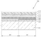
도 1은 본 발명의 일 실시예에 관한 유기 발광 표시 장치를 도시한 개략적인 단면도이다.1 is a schematic cross-sectional view illustrating an organic light emitting display device according to an embodiment of the present invention.
도 1을 참조하면 유기 발광 표시 장치(100)는 기판(101), 제1 전극(110), 광반사 부재(120), 중간층(114) 및 제2 전극(115)을 포함한다.Referring to FIG. 1, an
각 부재의 구성에 대하여 구체적으로 설명하기로 한다.The configuration of each member will be described in detail.
기판(101)은 SiO2를 주성분으로 하는 투명한 유리 재질로 이루어질 수 있다. 기판(101)은 반드시 이에 한정되는 것은 아니며 투명한 플라스틱 재질로 형성할 수도 있다. 이 때 기판(101)을 형성하는 플라스틱 재질은 다양한 유기물들 중 선택된 하나 이상일 수 있다.The
기판(101)상에 버퍼층(102)이 형성된다. 버퍼층(102)은 기판(101)을 통한 불순 원소의 침투를 방지하며 기판(101)상부에 평탄한 면을 제공하는 것으로서, 이러한 역할을 수행할 수 있는 다양한 물질로 형성될 수 있다. 일례로, 버퍼층(102)은 실리콘 옥사이드, 실리콘 나이트라이드, 실리콘 옥시나이트라이드, 알루미늄옥사이드, 알루미늄나이트라이드, 티타늄옥사이드 또는 티타늄나이트라이드 등의 무기물이나, 폴리이미드, 폴리에스테르, 아크릴 등의 유기물을 함유할 수 있고, 예시한 재료들 중 복수의 적층체로 형성될 수 있다. 또한 버퍼층(102)은 필수 구성요소는 아니며, 필요에 따라서는 구비되지 않을 수도 있다.A
버퍼층(102)상에 제1 절연막(106)이 형성된다. 제1 절연막(106)은 실리콘 옥사이드 또는 실리콘 나이트라이드 등과 같은 절연막을 이용하여 형성한다.A first
제1 절연막(106)상에 소정의 크기를 갖는 광반사 부재(120)가 형성된다. 광반사 부재(120)는 가시 광선을 일부 반사하고 일부는 투과하도록 형성된다. 광반사 부재(120)는 Al 또는 Ag를 함유하는 박막으로 형성될 수 있다.A
구체적으로 광반사 부재(120)는 후술한 중간층(114)의 전체영역이 아닌 일 영역에만 중첩되도록 형성된다. 또한 이를 위하여 광반사 부재(120)는 제1 전극(110)보다 작게 형성되는 것이 바람직하다.Specifically, the
광반사 부재(120)상에 제2 절연막(116)이 형성된다. 제2 절연막(116)은 광반사 부재(120)을 덮으면서 제1 절연막(106)상에 형성된다. 제2 절연막(116)은 다양한 절연물질을 이용하여 형성할 수 있고, 구체적인 예로서 실리콘 옥사이드 또는 실리콘 나이트라이드 등과 같은 절연막을 이용하여 형성한다.A second
제1 전극(110)은 제2 절연막(116)상에 형성된다. 제1 전극(110)은 투과형 도전물로 형성한다. 구체적으로 제1 전극(110)은 ITO, IZO, ZnO, In2O3, IGO 또는 AZO를 이용하여 형성할 수 있다.The
중간층(114)이 제1 전극(110)상에 형성된다. 중간층(114)은 가시 광선을 구현하도록 유기 발광층을 구비한다.An intermediate layer 114 is formed on the
중간층(114)은 저분자 또는 고분자 유기막으로 형성될 수 있다. 중간층(114)이 저분자 유기막으로 형성되는 경우, 정공 주입층(HIL: Hole Injection Layer), 정공 수송층(HTL: Hole Transport Layer), 유기 발광층, 전자 수송층(ETL: Electron Transport Layer), 전자 주입층(EIL: Electron Injection Layer) 등을 구비할 수 있다.The intermediate layer 114 may be formed of a low-molecular or polymer organic film. When the intermediate layer 114 is formed of a low molecular organic layer, a hole injection layer (HIL), a hole transport layer (HTL), an organic light emitting layer, an electron transport layer (ETL) (EIL: Electron Injection Layer) or the like.
정공 주입층(HIL)은 구리프탈로시아닌 등의 프탈로시아닌 화합물 또는 스타버스트(Starburst)형 아민류인 TCTA, m-MTDATA, m-MTDAPB 등으로 형성할 수 있다.The hole injection layer (HIL) may be formed of a phthalocyanine compound such as copper phthalocyanine or starburst type amines such as TCTA, m-MTDATA, and m-MTDAPB.
정공 수송층(HTL)은 N,N'-비스(3-메틸페닐)- N,N'-디페닐-[1,1-비페닐]-4,4'-디아민(TPD), N,N'-디(나프탈렌-1-일)-N,N'-디페닐 벤지딘(α-NPD)등으로 형성될 수 있다.The hole transporting layer (HTL) may be formed of a material selected from the group consisting of N, N'-bis (3-methylphenyl) -N, N'-diphenyl- [1,1-biphenyl] -4,4'- diamine (TPD) Di (naphthalen-1-yl) -N, N'-diphenylbenzidine (? -NPD).
전자 주입층(EIL)은 LiF, NaCl, CsF, Li2O, BaO, Liq 등의 물질을 이용하여 형성할 수 있다.The electron injection layer (EIL) can be formed using materials such as LiF, NaCl, CsF, Li2O, BaO, and Liq.
전자 수송층(ETL)은 Alq3를 이용하여 형성할 수 있다.The electron transport layer (ETL) can be formed using Alq3.
유기 발광층은 호스트 물질과 도판트 물질을 포함할 수 있다.The organic light emitting layer may include a host material and a dopant material.
유기 발광층의 호스트 물질로는 트리스(8-히드록시-퀴놀리나토)알루미늄 (Alq3), 9,10-디(나프티-2-일)안트라센 (AND), 3-Tert-부틸-9,10-디(나프티-2-일)안트라센 (TBADN), 4,4'-비스(2,2-디페닐-에텐-1-일)-4,4'-디메틸페닐 (DPVBi), 4,4'-비스Bis(2,2-디페닐-에텐-1-일)-4,4'-디메틸페닐 (p-DMDPVBi), Tert(9,9-디아릴플루오렌)s (TDAF), 2-(9,9'-스피로비플루오렌-2-일)-9,9'-스피로비플루오렌 (BSDF), 2,7-비스(9,9'-스피로비플루오렌-2-일)-9,9'-스피로비플루오렌 (TSDF), 비스(9,9-디아릴플루오렌)s (BDAF), 4,4'-비스(2,2-디페닐-에텐-1-일)-4,4'-디-(tert-부틸)페닐 (p-TDPVBi), 1,3-비스(카바졸-9-일)벤젠 (mCP), 1,3,5-트리스(카바졸-9-일)벤젠 (tCP), 4,4',4"-트리스(카바졸-9-일)트리페닐아민 (TcTa), 4,4'-비스(카바졸-9-일)비페닐 (CBP), 4,4'-비스Bis(9-카바졸일)-2,2'-디메틸-비페닐 (CBDP), 4,4'-비스(카바졸-9-일)-9,9-디메틸-플루오렌 (DMFL-CBP), 4,4'-비스(카바졸-9-일)-9,9-비스bis(9-페닐-9H-카바졸)플루오렌 (FL-4CBP), 4,4'-비스(카바졸-9-일)-9,9-디-톨일-플루오렌 (DPFL-CBP), 9,9-비스(9-페닐-9H-카바졸)플루오렌 (FL-2CBP) 등이 사용될 수 있다.Examples of the host material of the organic light emitting layer include tris (8-hydroxy-quinolinato) aluminum (Alq3), 9,10-di (naphthi- 2-yl) anthracene (AND), 3-tert- Bis (2,2-diphenyl-ethan-1-yl) -4,4'-dimethylphenyl (DPVBi), 4,4'- Dimethylphenyl (p-DMDPVBi), Tert (9,9-diarylfluorene) s (TDAF), 2- (9- , 9'-spirobifluoren-2-yl) -9,9'-spirobifluorene (BSDF), 2,7- (TSDF), bis (9,9-diarylfluorene) s (BDAF), 4,4'-bis (2,2-diphenyl-ethen- (Carbazole-9-yl) benzene (mCP), 1,3,5-tris (carbazole-9-yl) Benzene (tCP), 4,4 ', 4 "-tris (carbazol-9-yl) triphenylamine (TcTa), 4,4'-bis (carbazol- , 4'-bis (9-carbazolyl) -2,2'-dimethyl-biphenyl (CBDP), 4,4'-bis (carbazol- (9-phenyl-9H-carbazole) fluorene (FL-4CBP), 4,4'-bis Bis (9-phenyl-9H-carbazol) fluorene (FL-2CBP), etc., Can be used.
유기 발광층의 도판트 물질로는 DPAVBi (4,4'-비스[4-(디-p-톨일아미노)스티릴]비페닐), ADN (9,10-디(나프-2-틸)안트라센), TBADN (3-터트-부틸-9,10-디(나프-2-틸)안트라센) 등이 사용될 수 있다.Examples of the dopant material of the organic light emitting layer include DPAVBi (4,4'-bis [4- (di-p-tolylamino) styryl] biphenyl), ADN (9,10-di (naphth- , And TBADN (3-tert-butyl-9,10-di (naphth-2-yl) anthracene).
중간층(114)의 크기는 광반사 부재(120)보다 크다. 즉, 광반사 부재(120)는 중간층(114)의 전체 면적인 아닌 중간층(114)의 일 영역에만 중첩되도록 형성된다. 이를 통하여 중간층(114)에서 발생한 가시 광선 중 하부, 즉 기판(101)을 향하는 광의 일부는 광반사 부재(120)에 도달하고 일부는 광반사 부재(120)가 존재하지 않는 영역의 제1 절연막(106), 제2 절연막(116) 또는 버퍼층(102)에 도달하게 된다.The size of the intermediate layer 114 is larger than that of the
또한 광반사 부재(120)는 제1 전극(110)보다 작게 형성되는 것이 바람직하다.The
제2 전극(115)은 중간층(114)상에 형성된다. 제2 전극(115)은 Ag, Mg, Al, Pt, Pd, Au, Ni, Nd, Ir, Cr, Li, 또는 Ca의 금속으로 형성될 수 있다.A second electrode (115) is formed on the intermediate layer (114). The
본 실시예의 유기 발광 표시 장치(100)의 동작 및 효과에 대하여 간략하게 설명하기로 한다.The operation and effects of the organic light emitting
제1 전극(110) 및 제2 전극(115)에 전압이 인가되면 제1 전극(110) 및 제2 전극(115)과 전기적으로 연결된 중간층(114)에서 가시 광선이 발광한다. 이러한 가시 광선의 일부는 제1 전극(110)을 향하고 또 다른 일부는 제2 전극(115)을 향하게 된다. 중간층(114)에서 발생한 가시 광선 중 제1 전극(110)을 향하는 광은 제1 전극(110)을 대부분 투과하여 광반사 부재(120)에 도달한다. 광반사 부재(120)에 도달한 광은 일부는 반사되어 제2 전극(115)을 향하게 된다. 그리고 제2 전극(115)을 향하게 된 광은 다시 제2 전극(115)에서 반사되어 제1 전극(110)방향으로 진행하여 광반사 부재(120)에서 반사된다. 즉 중간층(114)에서 발생한 가시 광선은 제1 공진 영역(SR)에서 제2 전극(115)과 광반사 부재(120)사이의 공간에서 공진을 하게된다. 이를 통하여 중간층(114)에서 발생한 가시 광선의 광효율이 향상된다. 즉, 사용자측으로 취출되는 가시 광선의 양이 증가하여 광취출 효율이 향상된다.When a voltage is applied to the
특히 광반사 부재(120)를 이용한 강한 공진 현상을 이용하여 중간층(114)에서 발생한 가시 광선의 색좌표 특성을 개선하여 선명한 가시 광선을 구현할 수 있다.Particularly, by using a strong resonance phenomenon using the
이 때 제1 전극(110)과 광반사 부재(120)사이에는 제2 절연막(116)이 배치되어 제1 전극(110)과 광반사 부재(120)사이의 접촉으로 인하여 발생할 수 있는 광간섭을 억제하고, 제1 전극(110)과 광반사 부재(120)사이의 공간에서도 광공진 효과를 발생하는 것이 가능하다.The second
또한 본 실시예의 유기 발광 표시 장치(100)는 기판(101)방향으로 가시 광선이 취출되는 배면 발광 타입일 수 있는데, 광반사 부재(120)가 가시 광선의 일부는 반사하고 일부는 반사하도록 하여 기판(101)방향으로 최종적으로 가시 광선이 취출될 수 있다.Also, the organic light emitting
한편, 광반사 부재(120)는 중간층(114)의 전체가 아닌 일 영역에만 대응되도록 형성되므로 중간층(114)에서 발생한 가시 광선은 광반사 부재(120)가 존재하지 않는 영역으로 향하게 된다 이러한 가시 광선은 절연막의 표면, 즉 제1 절연막(106)의 표면, 제2 절연막(116)의 표면 또는 버퍼층(102)의 표면에서 일부가 반사되어 제2 전극(115)을 향하게 된다. 제2 전극(115)을 향하여 진행한 광은 반사되어 다시 제1 전극(110)방향으로 진행하여 상기 절연막의 표면에서 일부 반사된다. 즉 중간층(114)에서 발생한 가시 광선은 제2 공진 영역(WR)에서 제2 전극(115)과 제2 절연막(116)사이의 공간, 제2 전극(115)과 제1 절연막(106)사이의 공간 또는 제2 전극(115)과 버퍼층(102)사이의 공간에서 공진을 하게된다. 이를 통하여 중간층(114)에서 발생한 가시 광선의 광효율이 향상된다. 특히, 이러한 공진은 상기 광반사 부재(120)를 이용한 강한 공진에 비하면 광투과율이 높은 약한 공진이다. 이를 통하여 중간층(114)에서 발생한 가시 광선이 사용자의 시야각에 따라 변하는 정도를 최소화한다. 즉, 사용자가 볼 때 정면과 측면에서의 유기 발광 표시 장치(100)의 휘도 변화를 억제한다.Since the
또한 본 실시예의 유기 발광 표시 장치(100)가 배면 발광 타입인 경우 제2 공진 영역(WR)에는 광반사 부재(120)가 형성되지 않아 가시 광선의 투과율이 향상되고 이를 통하여 유기 발광 표시 장치(100)의 휘도 감소를 억제한다.When the
본 발명에서는 광공진 효과를 이용하여 유기 발광 표시 장치(100)의 화질 특성을 향상한다. 특히, 금속과 같은 물질로 형성된 광반사 부재(120)를 이용한 강한 공진과 절연막(106,116)을 이용한 약한 공진을 동시에 구현하여 선명한 색을 구현하여 색특성을 향상하면서 시야각에 따른 휘도 변화를 억제한다. 결과적으로 유기 발광 표시 장치(100)의 화질 특성을 현저하게 향상할 수 있다.In the present invention, the image quality characteristic of the
이 때 강한 공진을 발생하는 제1 공진 영역(SR)과 약한 공진을 발생하는 제2 공진 영역(WR)의 면적은 원하는 가시 광선의 특성에 따라 달라질 수 있는데, 가시 광선을 구현하는 전체 면적에서 제1 공진 영역(SR)이 25 내지 70 퍼센트 일 수 있고, 바람직하게는 50 퍼센트일 수 있다.The area of the first resonance area SR that generates strong resonance and the area of the second resonance area WR that generates weak resonance may vary depending on the characteristics of a desired visible light. One resonance region (SR) may be 25 to 70 percent, and preferably 50 percent.
도 2는 본 발명의 다른 실시예에 관한 유기 발광 표시 장치를 도시한 개략적인 단면도이다.2 is a schematic cross-sectional view illustrating an organic light emitting display according to another embodiment of the present invention.
도 2를 참조하면 유기 발광 표시 장치(200)는 기판(201), 제1 전극(210), 광반사 부재(220), 중간층(214) 및 제2 전극(215)을 포함한다. 또한 유기 발광 표시 장치(200)는 복수의 부화소를 구비하는데, 구체적으로 청색 부화소(B), 녹색 부화소(G) 및 적색 부화소(R)를 구비한다. 또한 제1 전극(210), 중간층(214) 및 제2 전극(215)은 부화소(B, G, R)들 각각에 대응되도록 형성된다.Referring to FIG. 2, the
각 부재의 구성에 대하여 구체적으로 설명하기로 한다. 설명의 편의를 위하여 전술한 실시예와 상이한 점을 중심으로 설명하기로 한다.The configuration of each member will be described in detail. For convenience of explanation, the description will be focused on the differences from the above-described embodiment.
기판(201)상에 버퍼층(202)이 형성된다. 버퍼층(202)은 모든 부화소들에 걸쳐 공통적으로 형성되는 것이 바람직하다. 버퍼층(202)상에 제1 절연막(206)이 형성된다. 제1 절연막(206)은 모든 부화소들에 걸쳐 공통으로 형성된다.A
광반사 부재(220)는 제1 절연막(206)상에 소정의 크기를 갖도록 형성된다. 특히, 광반사 부재(220)는 청색 부화소(B)에만 형성될 수 있다. 그러나 본 발명은 이에 한정되지 않고 모든 부화소들에 광반사 부재(220)가 형성될 수도 있다.The
광반사 부재(220)는 가시 광선을 일부 반사하고 일부는 투과하도록 형성된다. 광반사 부재(220)는 Al 또는 Ag를 함유하는 박막으로 형성될 수 있다. 광반사 부재(220)는 중간층(214B)의 전체 면적인 아닌 중간층(214B)의 일부와 중첩되도록 형성된다.The
광반사 부재(220)상에 제2 절연막(216)이 형성된다. 제2 절연막(216)은 광반사 부재(220)을 덮으면서 제1 절연막(206)상에 모든 부화소들에 걸쳐 공통적으로 형성된다.A second insulating film 216 is formed on the
제1 전극(210)은 제2 절연막(216)상에 형성된다. 제1 전극(210)은 각 부화소(R, G, B)들에 대응되는데, 서로 이격된 아일랜드 패턴으로 형성될 수 있다.The
제1 전극(210)상에 절연물을 이용하여 화소 정의막(213)이 형성된다. 이 때 화소 정의막(213)은 제1 전극(210)의 상면을 노출하도록 개구를 갖도록 형성된다.A
중간층(214B, 214R, 214G)이 노출된 제1 전극(210)의 상면에 형성된다. 구체적으로 중간층(214B)은 청색 부화소(B)에 대응되고, 중간층(214G)은 녹색 부화소(G)에 대응되고, 중간층(214R)은 적색 부화소(R)에 대응된다.
중간층(214B, 214R, 214G)은 가시 광선을 구현하도록 유기 발광층을 구비하는데, 구체적으로 중간층(214B)은 청색 가시 광선을 발광하는 유기 발광층, 중간층(214G)은 녹색 가시 광선을 발광하는 유기 발광층, 중간층(214R)은 적색 가시 광선을 발광하는 유기 발광층을 각각 구비한다.The
제2 전극(215)은 중간층(214B, 214R, 214G)상에 형성되는데, 모든 부화소들에 걸쳐 공통적으로 형성되는 것이 바람직하다.The
본 실시예의 유기 발광 표시 장치(200)는 중간층(214B)에서 발생한 가시 광선이 제1 공진 영역(SR)에서 제2 전극(215)과 광반사 부재(220)사이의 공간에서 공진을 하게된다. 이를 통하여 중간층(214)에서 발생한 가시 광선의 광효율이 향상된다. 특히 광반사 부재(220)를 이용한 강한 공진 현상을 이용하여 중간층(214B)에서 발생한 청색 가시 광선의 색좌표 특성을 개선하여 선명한 가시 광선을 구현할 수 있다.The visible light generated in the
한편, 중간층(214B, 214G, 214R)에서 발생한 가시 광선은 제2 공진 영역(WR)에서 제2 전극(215)과 제2 절연막(216)사이의 공간, 제2 전극(215)과 제1 절연막(206)사이의 공간 또는 제2 전극(215)과 버퍼층(202)사이의 공간에서 공진을 하게 된다. 이를 통하여 중간층(214B, 214G, 214R)에서 발생한 가시 광선의 광효율이 향상된다. 특히, 중간층(214B, 214G, 214R)에서 발생한 가시 광선이 사용자의 시야각에 따라 변하는 정도를 최소화한다. 즉, 사용자가 볼 때 정면과 측면에서의 유기 발광 표시 장치(200)의 휘도 변화를 억제한다.The visible light generated in the
본 발명에서는 광공진 효과를 이용하여 유기 발광 표시 장치(200)의 화질 특성을 향상한다. 특히, 통상의 유기 발광 표시 장치에서 청색 부화소의 색특성의 감소가 문제되는데 본 실시예의 유기 발광 표시 장치(200)는 광반사 부재(220)를 이용한 강한 공진으로 청색 부화소(B)에서의 색특성을 향상한다. 이와 동시에 청색 부화소(B)내에 제2 공진 영역(WR)에서는 절연막을 이용한 약한 공진이 발생하여 시야각에 따른 휘도 감소 및 화질 저하를 방지한다.In the present invention, the image quality characteristic of the
또한 다른 부화소(R, G)에서는 광반사 부재가 아닌 절연막을 이용한 약한 공진으로 시야각에 따라 휘도 변화를 억제한다.In addition, in the other sub-pixels R and G, a weak resonance using an insulating film rather than a light reflecting member suppresses the change in luminance according to the viewing angle.
결과적으로 화질 특성이 향상된 유기 발광 표시 장치(200)를 구현할 수 있다. 본 발명은 이에 한정되지 않고 부화소들의 설계 조건에 따라 청색 부화소(B)와 함께, 녹색 부화소(G) 또는 적색 부화소(R)에도 광반사 부재(220)를 배치할 수 있다.As a result, the
도 3은 본 발명의 또 다른 실시예에 관한 유기 발광 표시 장치를 도시한 개략적인 단면도이다.3 is a schematic cross-sectional view illustrating an organic light emitting display device according to another embodiment of the present invention.
도 3을 참조하면 유기 발광 표시 장치(300)는 기판(301), 제1 전극(310), 광반사 부재(320), 중간층(314) 및 제2 전극(315)을 포함한다. 설명의 편의를 위하여 전술한 실시예와 상이한 점을 중심으로 설명하기로 한다.Referring to FIG. 3, the
기판(301)상에 버퍼층(302)이 형성된다. 버퍼층(302)상에 소정의 크기를 갖는 광반사 부재(320)가 형성된다. 구체적으로 광반사 부재(320)는 중간층(314)의 전체가 아닌 일 영역과 중첩되도록 형성된다.A
광반사 부재(320)상에 제2 절연막(306)이 형성된다. 제2 절연막(306)은 광반사 부재(320)를 덮으면서 버퍼층(302)상에 형성된다.A second insulating
제2 절연막(306)상에 제3 절연막(316)이 형성된다. 다양한 절연물질을 이용하여 형성할 수 있고, 구체적인 예로서 실리콘 옥사이드 또는 실리콘 나이트라이드 등과 같은 절연막을 이용하여 형성한다.A third
제1 전극(310)은 제3 절연막(316)상에 형성된다. 중간층(314)이 제1 전극(310)상에 형성된다. 중간층(314)은 가시 광선을 구현하도록 유기 발광층을 구비한다.The
중간층(314)의 크기는 광반사 부재(320)보다 크다. 즉, 광반사 부재(320)는 중간층(314)의 전체 면적인 아닌 중간층(314)의 일 영역에만 중첩되도록 형성된다. 이를 통하여 중간층(314)에서 발생한 가시 광선 중 하부, 즉 기판(301)을 향하는 광의 일부는 광반사 부재(320)에 도달하고 일부는 광반사 부재(320)가 존재하지 않는 영역의 제2 절연막(306), 제3 절연막(316) 또는 버퍼층(302)에 도달하게 된다.The size of the
또한 광반사 부재(320)는 제1 전극(310)보다 작게 형성되는 것이 바람직하다.The
제2 전극(315)은 중간층(314)상에 형성된다.A
본 실시예의 유기 발광 표시 장치(300)는 제1 공진 영역(SR)에서 제2 전극(315)과 광반사 부재(320)사이의 공간에서 발생하는 강한 공진 현상을 이용하여 중간층(314)에서 발생한 가시 광선의 색좌표 특성을 개선하여 선명한 가시 광선을 구현할 수 있다.The organic
한편, 중간층(314)에서 발생한 가시 광선은 제2 공진 영역(WR)에서 제2 전극(315)과 제3 절연막(316)사이의 공간, 제2 전극(315)과 제2 절연막(306) 사이의 공간 또는 제2 전극(315)과 버퍼층(302)사이의 공간에서 약한 공진을 하게된다. 이를 통하여 중간층(314)에서 발생한 가시 광선이 사용자의 시야각에 따라 변하는 정도를 최소화한다. 즉, 사용자가 볼 때 정면과 측면에서의 유기 발광 표시 장치(300)의 휘도 변화를 억제한다.A visible ray generated in the
한편 본 실시예에서는 제1 전극(310)과 광반사 부재(320)사이에 제2 절연막(306) 및 제3 절연막(316)이 배치되어 제1 전극(310)과 광반사 부재(320)의 접촉으로 인하여 발생할 수 있는 광간섭을 억제하고, 제1 전극(310)과 광반사 부재(120)사이의 공간, 특히 제2 절연막(306)과 제3 절연막(316)의 계면에서도 광공진을 발생하여 유기 발광 표시 장치(300)의 화질 특성 향상을 증대한다.A second insulating
도시하지 않았으나 본 실시예의 유기 발광 표시 장치(300)도 도 2의 구성과 유사하게 복수의 부화소들을 구비하고 광반사 부재(320)를 청색 부화소에만 형성할 수 있음은 물론이다.Although not shown, it is needless to say that the
도 4는 본 발명의 또 다른 실시예에 관한 유기 발광 표시 장치를 도시한 개략적인 단면도이다.4 is a schematic cross-sectional view illustrating an organic light emitting display according to another embodiment of the present invention.
도 4를 참조하면 유기 발광 표시 장치(400)는 기판(401), 박막 트랜지스터(TFT), 제1 전극(410), 광반사 부재(420), 중간층(414) 및 제2 전극(415)를 포함한다.4, the
박막 트랜지스터(TFT)는 활성층(403), 게이트 전극(405), 소스 전극(407) 및 드레인 전극(408)을 구비한다.The thin film transistor TFT has an
또한 유기 발광 표시 장치(400)는 하나 이상의 캐패시터(418)를 포함할 수 있고, 캐패시터(418)은 제1 캐패시터 전극(411) 및 제2 캐패시터 전극(413)을 구비한다.The organic
기판(401)상에 버퍼층(402)이 형성된다. 버퍼층(402)상에 소정의 크기를 갖는 광반사 부재(420)가 형성된다. 구체적으로 광반사 부재(420)는 중간층(414)의 전체가 아닌 일 영역과 중첩되도록 형성된다.A buffer layer 402 is formed on the
광반사 부재(420)상에 제2 절연막(406)이 형성된다. 제2 절연막(406)은 광반사 부재(420)를 덮으면서 버퍼층(402)상에 형성된다.A second insulating film 406 is formed on the
제2 절연막(406)상에 활성층(403)이 형성된다. 또한 제2 절연막(406)상에 제1 캐패시터 전극(411)이 형성된다. 제1 캐패시터 전극(411)은 활성층(403)과 동일한 재료로 형성되는 것이 바람직하다.An
제2 절연막(406)상에 활성층(403) 및 제1 캐패시터 전극(411)을 덮도록 제3 절연막(416)이 형성된다.A third
제2 절연막(406)상에 게이트 전극(405), 제1 전극(410) 및 제2 캐패시터 전극(413)이 형성된다.A
게이트 전극(405)은 제1 도전층(405a) 및 제2 도전층(405b)을 구비한다. 제1 도전층(405a)은 투과형 도전 물질을 함유하는데 구체적으로 인듐틴옥사이드(indium tin oxide: ITO), 인듐징크옥사이드(indium zinc oxide: IZO), 징크옥사이드(zinc oxide: ZnO), 인듐옥사이드(indium oxide: In2O3), 인듐갈륨옥사이드(indium gallium oxide: IGO), 및 알루미늄징크옥사이드(aluminum zinc oxide: AZO)을 포함하는 그룹에서 선택된 적어도 하나 이상을 함유할 수 있다. 제2 도전층(405b) 은 제1 도전층(405a)상에 Mo, MoW, Al계 합금 등과 같은 금속 또는 금속의 합금을 함유하도록 형성할 수 있으나, 이에 한정되는 것은 아니다.The
제1 전극(410)은 투과형 도전 물질을 함유하는데 제1 도전층(405a)과 동일한 물질로 형성할 수 있다. 제1 전극(410)의 상부의 소정의 영역에는 도전부(410a)가 배치되는데 도전부(410a)는 제2 도전층(405b) 과 동일한 재질로 형성된다.The
제2 캐패시터 전극(413)은 제1 층(413a) 및 제2 층(413b)을 구비하는데, 제1 층(413a)은 제1 도전층(405a)과 동일한 재질로 형성되고 제2 층(413b)은 제2 도전층(405b) 과 동일한 재질로 형성된다. 또한 제2 층(413b)을 제1 전극(410)과 같이 2층 구조 또는 3층 구조로 할 수 있음은 물론이다.The
제2 층(413b)은 제1 층(413a)보다 작게 제1 층(413a)상에 형성된다. 또한 제2 캐패시터 전극(413)은 제1 캐패시터 전극(411)과 중첩되고 제1 캐패시터 전극(411)보다 작게 형성된다.The
제1 전극(410), 게이트 전극(405) 및 제2 캐패시터 전극(413)상에 층간 절연막(417)이 형성된다. 층간 절연막(417)은 유기물 또는 무기물 등 다양한 재질의 절연 물질을 함유할 수 있다. 한편 본 발명은 도시하지 않았으나 층간 절연막(417)을 복층 구조로 형성할 수 있다. 예를들면 층간 절연막(417)을 무기막/유기막의 2층 이상의 적층 구조로 형성할 수도 있다. 이를 통하여 층간 절연막(417)의 절연 및 보호 효과를 증대한다. 이 때 층간 절연막(417)을 형성하는 무기막은 실리콘 옥사이드 또는 실리콘 나이트라이드를 함유할 수 있다.An interlayer insulating
층간 절연막(417)상에 소스 전극(407) 및 드레인 전극(408)이 형성된다. 소스 전극(407) 및 드레인 전극(408)은 활성층(403)과 연결되도록 형성된다.A
또한 소스 전극(407) 및 드레인 전극(408) 중 어느 하나의 전극은 제1 전극(410)과 전기적으로 연결되는데 도 4에는 드레인 전극(408)이 제1 전극(410)과 전기적으로 연결된 것이 도시되어 있다. 구체적으로 드레인 전극(408)은 도전부(410a)와 접한다.One of the
층간 절연막(417)상에 박막 트랜지스터(TFT) 및 캐패시터(418)를 덮도록 화소 정의막(419)이 형성된다.A
화소 정의막(419)은 제1 전극(410)의 상면에 대응되는 소정의 개구부(419a)를 갖도록 형성되고, 화소 정의막(419)의 개구부(419a)를 통하여 노출된 제1 전극(410)상에 중간층(414)이 형성된다.The
중간층(414)상에 제2 전극(415)이 형성된다.A
도시하지 않았으나 제2 전극(415)상에 밀봉 부재(미도시)가 배치될 수 있다. 밀봉 부재는 제1 전극(410), 중간층(414) 또는 제2 전극(415)을 외부의 이물 또는 충격으로 인한 손상을 방지하도록 형성되고 유리, 금속 박막 등으로 형성되거나 유기물과 무기물의 적층 구조로 형성될 수도 있다.Although not shown, a sealing member (not shown) may be disposed on the
본 실시예의 유기 발광 표시 장치(400)는 제1 공진 영역(SR)에서 제2 전극(415)과 광반사 부재(420)사이의 공간에서 발생하는 강한 공진 현상을 이용하여 중간층(414)에서 발생한 가시 광선의 색좌표 특성을 개선하여 선명한 가시 광선을 구현할 수 있다.The organic
한편, 중간층(414)에서 발생한 가시 광선은 제2 공진 영역(WR)에서 제2 전극(415)과 제3 절연막(416)사이의 공간, 제2 전극(415)과 제2 절연막(406) 사이의 공간 또는 제2 전극(415)과 버퍼층(402)사이의 공간에서 약한 공진을 하게된다. 이를 통하여 중간층(414)에서 발생한 가시 광선이 사용자의 시야각에 따라 변하는 정도를 최소화한다. 즉, 사용자가 볼 때 정면과 측면에서의 유기 발광 표시 장치(400)의 휘도 변화를 억제한다.A visible ray generated in the
한편 본 실시예에서는 제1 전극(410)과 광반사 부재(420)사이에 제2 절연막(406) 및 제3 절연막(416)이 배치되어 제1 전극(410)과 광반사 부재(420)사이의 광간섭을 억제하고, 제1 전극(410)과 광반사 부재(420)사이의 공간, 특히 제2 절연막(406)과 제3 절연막(416)의 계면에서도 광공진을 발생하여 유기 발광 표시 장치(400)의 화질 특성 향상을 증대한다.A second insulating layer 406 and a third
도시하지 않았으나 본 실시예의 유기 발광 표시 장치(400)도 복수의 부화소를 구비할 수 있고, 도 2에 도시된 것과 같이 청색 부화소에만 광반사 부재(420)를 형성할 수 있음은 물론이다.Although not shown, the
또한 본 실시예에서는 광반사 부재(420)상에 제2 절연막(406)을 형성하고, 제2 절연막(406)상에 활성층(403) 및 제1 캐패시터 전극(411)을 형성한다. 이를 통하여 활성층(403) 및 제1 캐패시터 전극(411)에 손상을 주지 않고 광반사 부재(420)를 간단한 공정으로 형성할 수 있다.A second insulating layer 406 is formed on the
또한 게이트 전극(405)과 캐패시터(418)를 동일한 재료로 동일한 층에 형성하여 유기 발광 표시 장치(200)의 두께를 용이하게 감소할 수 있다.Also, the thickness of the organic light emitting
한편, 본 실시예의 유기 발광 표시 장치(400)는 중간층(414)에서 발생한 가시 광선이 기판(401)방향으로 구현되는 배면 발광 타입일 수 있는데, 박막 트랜지스터를 중간층(414)과 중첩되지 않고 이격되도록 하여 중간층(414)에서 발생한 가시 광선이 용이하게 기판(401)을 통하여 사용자에게 도달할 수 있다.The
물론 본 발명은 이에 한정되지 않고 중간층(414)에서 발생한 가시 광선이 제2 전극(415)을 통과하여 사용자에게 화상으로 인식되는 전면 발광 타입일 수도 있다.The present invention is not limited to this, and may be a front emission type in which visible light generated in the
본 발명은 도면에 도시된 실시예를 참고로 설명되었으나 이는 예시적인 것에 불과하며, 당해 기술 분야에서 통상의 지식을 가진 자라면 이로부터 다양한 변형 및 균등한 다른 실시예가 가능하다는 점을 이해할 것이다. 따라서, 본 발명의 진정한 기술적 보호 범위는 첨부된 특허청구범위의 기술적 사상에 의하여 정해져야 할 것이다.While the present invention has been described with reference to exemplary embodiments, it is to be understood that the invention is not limited to the disclosed exemplary embodiments, but, on the contrary, is intended to cover various modifications and equivalent arrangements included within the spirit and scope of the invention. Accordingly, the true scope of the present invention should be determined by the technical idea of the appended claims.
100, 200, 300, 400: 유기 발광 표시 장치
101, 201, 301, 401: 기판
110, 210, 310, 410: 제1 전극
TFT: 박막 트랜지스터
114, 214, 314, 414: 중간층
115, 215, 315, 415: 제2 전극
120, 220, 320, 420: 광반사 부재
106, 206: 제1 절연막
116, 216, 306: 제2 절연막
316: 제3 절연막100, 200, 300, 400: organic light emitting display
101, 201, 301, 401: substrate
110, 210, 310, 410: a first electrode
TFT: Thin film transistor
114, 214, 314, 414:
115, 215, 315, 415:
120, 220, 320, 420:
106, and 206: a first insulating film
116, 216, and 306:
316: Third insulating film
Claims (20)
Translated fromKorean상기 기판 상에 형성된 제1 전극;
상기 제1 전극 상에 배치되는 제2 전극;
상기 제1 전극과 상기 제2 전극 사이에 배치되고 상기 제1 전극과 상기 제2 전극과 전기적으로 연결되고 유기 발광층을 구비하는 중간층;
상기 중간층의 전체 영역 보다 작은 상기 중간층의 일 영역과 중첩되도록 형성된 광반사 부재; 및
상기 광반사 부재와 상기 제1 전극 사이에 배치된 제2 절연막을 포함하고,
상기 제2 절연막은 상기 제1 전극과 중첩된 영역에서의 서로 다른 값인 제1 두께 및 제2 두께를 갖고
상기 제2 절연막의 상기 제1 두께는 상기 광반사 부재와 제1 전극 사이의 거리이고,
상기 제2 절연막의 상기 제2 두께는 상기 제2 절연막의 영역 중 상기 제1 전극과 중첩되고 상기 광반사 부재와는 중첩되지 않는 영역에서의 두께인 것을 포함하는 유기 발광 표시 장치.Board;
A first electrode formed on the substrate;
A second electrode disposed on the first electrode;
An intermediate layer disposed between the first electrode and the second electrode and electrically connected to the first electrode and the second electrode and having an organic light emitting layer;
A light reflection member formed to overlap with one region of the intermediate layer which is smaller than the entire region of the intermediate layer; And
And a second insulating film disposed between the light reflecting member and the first electrode,
Wherein the second insulating film has a first thickness and a second thickness which are different values in a region overlapping with the first electrode
The first thickness of the second insulating film is a distance between the light reflecting member and the first electrode,
And the second thickness of the second insulating film is a thickness of a region overlapping with the first electrode of the region of the second insulating film and not overlapping with the light reflecting member.
상기 광반사 부재는 가시 광선의 일부는 반사시키고 일부는 투과시키는 유기 발광 표시 장치.The method according to claim 1,
Wherein the light reflection member reflects part of visible light and transmits part of visible light.
상기 광반사 부재는 상기 중간층보다 작게 형성되는 유기 발광 표시 장치.The method according to claim 1,
Wherein the light reflection member is formed to be smaller than the intermediate layer.
상기 광반사 부재는 상기 제1 전극보다 작게 형성되는 유기 발광 표시 장치.The method according to claim 1,
Wherein the light reflection member is formed to be smaller than the first electrode.
상기 기판과 상기 광반사 부재 사이에 배치된 제1 절연막을 더 포함하는 유기 발광 표시 장치.The method according to claim 1,
And a first insulating layer disposed between the substrate and the light reflection member.
상기 기판과 상기 제1 절연막 사이에 배치된 버퍼층을 더 포함하는 유기 발광 표시 장치.6. The method of claim 5,
And a buffer layer disposed between the substrate and the first insulating film.
상기 제2 절연막과 상기 제1 전극 사이에 배치된 제3 절연막을 더 포함하는 유기 발광 표시 장치.The method according to claim 1,
And a third insulating layer disposed between the second insulating layer and the first electrode.
상기 광반사 부재는 Ag 또는 Al을 함유하는 유기 발광 표시 장치.The method according to claim 1,
Wherein the light reflection member contains Ag or Al.
상기 제1 전극은 ITO, IZO, ZnO, In2O3, IGO 또는 AZO를 함유하는 유기 발광 표시 장치.The method according to claim 1,
Wherein the first electrode comprises ITO, IZO, ZnO, In2O3, IGO or AZO.
상기 유기 발광 표시 장치는 복수의 부화소들을 구비하고,
상기 제1 전극, 중간층 및 상기 제2 전극은 상기 부화소들 각각에 대응되도록 형성되고,
상기 광반사 부재는 상기 복수의 부화소들 중 적어도 하나의 부화소들에 대응되도록 배치되는 유기 발광 표시 장치.The method according to claim 1,
The OLED display device includes a plurality of sub-pixels,
The first electrode, the intermediate layer, and the second electrode are formed to correspond to the sub-pixels, respectively,
Wherein the light reflection member is arranged to correspond to at least one of the plurality of sub-pixels.
상기 복수의 부화소들은 서로 다른 종류의 색의 가시 광선을 구현하는 부화소들을 구비하고,
상기 광반사 부재는 상기 복수의 부화소들 중 어느 하나의 색의 가시 광선을 구현하는 부화소들에 대응되도록 배치되는 유기 발광 표시 장치.13. The method of claim 12,
Wherein the plurality of sub-pixels include sub-pixels for implementing visible light of different kinds of colors,
Wherein the light reflection member is disposed to correspond to the sub-pixels that emit visible light of any one of the plurality of sub-pixels.
상기 광반사 부재는 상기 복수의 부화소들 중 청색의 가시 광선을 구현하는 부화소들에 대응되도록 배치되는 유기 발광 표시 장치.14. The method of claim 13,
Wherein the light reflecting member is disposed to correspond to the sub-pixels of the plurality of sub-pixels that emit blue visible light.
상기 기판 상에 형성되고 상기 제1 전극과 전기적으로 연결되고, 활성층, 게이트 전극, 소스 전극 및 드레인 전극을 구비하는 박막 트랜지스터를 더 포함하는 유기 발광 표시 장치.The method according to claim 1,
And a thin film transistor formed on the substrate and electrically connected to the first electrode, the thin film transistor including an active layer, a gate electrode, a source electrode, and a drain electrode.
상기 광반사 부재가 상기 활성층 보다 상기 기판에 가깝게 배치되도록 상기 광반사 부재와 상기 활성층은 서로 상이한 층에 형성되는 유기 발광 표시 장치.16. The method of claim 15,
Wherein the light reflecting member and the active layer are formed on different layers so that the light reflecting member is closer to the substrate than the active layer.
상기 제1 전극은 상기 게이트 전극과 동일한 층 상에 형성되고, 상기 제1 전극은 상기 게이트 전극의 재료 중 적어도 일부를 함유하는 유기 발광 표시 장치.16. The method of claim 15,
Wherein the first electrode is formed on the same layer as the gate electrode, and the first electrode contains at least a part of the material of the gate electrode.
상기 게이트 전극은 제1 도전층 및 상기 제1 도전층 상에 형성되는 제2 도전층을 구비하고, 상기 제1 전극은 상기 제1 도전층과 동일한 재료로 상기 제1 도전층과 동일한 층 상에 형성되는 유기 발광 표시 장치.16. The method of claim 15,
Wherein the gate electrode comprises a first conductive layer and a second conductive layer formed on the first conductive layer, wherein the first electrode is formed of the same material as the first conductive layer on the same layer as the first conductive layer The organic light emitting display device comprising:
상기 중간층은 상기 박막 트랜지스터와 중첩되지 않고 이격되도록 형성되는 유기 발광 표시 장치.16. The method of claim 15,
Wherein the intermediate layer is formed to be spaced apart from the thin film transistor so as not to overlap with the thin film transistor.
상기 활성층과 동일한 층에 형성되는 제1 캐패시터 전극 및 상기 게이트 전극과 동일한 층에 형성되는 제2 캐패시터 전극을 구비하는 캐패시터를 더 포함하는 유기 발광 표시 장치.16. The method of claim 15,
And a capacitor including a first capacitor electrode formed on the same layer as the active layer and a second capacitor electrode formed on the same layer as the gate electrode.
Priority Applications (4)
| Application Number | Priority Date | Filing Date | Title |
|---|---|---|---|
| KR1020110132126AKR101880723B1 (en) | 2011-12-09 | 2011-12-09 | Organic light emitting display apparatus |
| US13/489,650US8937312B2 (en) | 2011-12-09 | 2012-06-06 | Organic light-emitting display apparatus |
| TW101130367ATWI580024B (en) | 2011-12-09 | 2012-08-22 | Organic light emitting display device |
| CN201210518142.8ACN103165646B (en) | 2011-12-09 | 2012-12-05 | Organic light-emitting display device |
Applications Claiming Priority (1)
| Application Number | Priority Date | Filing Date | Title |
|---|---|---|---|
| KR1020110132126AKR101880723B1 (en) | 2011-12-09 | 2011-12-09 | Organic light emitting display apparatus |
Publications (2)
| Publication Number | Publication Date |
|---|---|
| KR20130065316A KR20130065316A (en) | 2013-06-19 |
| KR101880723B1true KR101880723B1 (en) | 2018-07-23 |
Family
ID=48571157
Family Applications (1)
| Application Number | Title | Priority Date | Filing Date |
|---|---|---|---|
| KR1020110132126AActiveKR101880723B1 (en) | 2011-12-09 | 2011-12-09 | Organic light emitting display apparatus |
Country Status (4)
| Country | Link |
|---|---|
| US (1) | US8937312B2 (en) |
| KR (1) | KR101880723B1 (en) |
| CN (1) | CN103165646B (en) |
| TW (1) | TWI580024B (en) |
Families Citing this family (1)
| Publication number | Priority date | Publication date | Assignee | Title |
|---|---|---|---|---|
| DE102013106502A1 (en)* | 2013-06-21 | 2014-12-24 | Osram Opto Semiconductors Gmbh | Optoelectronic component, method for producing an optoelectronic component and mirror device |
Citations (3)
| Publication number | Priority date | Publication date | Assignee | Title |
|---|---|---|---|---|
| US20040263072A1 (en) | 2003-06-24 | 2004-12-30 | Joon-Young Park | Flat panel display |
| US20070205717A1 (en)* | 2006-03-06 | 2007-09-06 | Seiko Epson Corporation | Electroluminescent device |
| US20100193790A1 (en)* | 2009-01-30 | 2010-08-05 | Samsumg Mobile Display Co., Ltd. | Flat panel display apparatus and method of manufacturing the same |
Family Cites Families (10)
| Publication number | Priority date | Publication date | Assignee | Title |
|---|---|---|---|---|
| US7230594B2 (en)* | 2002-12-16 | 2007-06-12 | Eastman Kodak Company | Color OLED display with improved power efficiency |
| KR100704258B1 (en)* | 2004-06-02 | 2007-04-06 | 세이코 엡슨 가부시키가이샤 | Organic EL Devices and Electronic Devices |
| JP4419691B2 (en)* | 2004-06-02 | 2010-02-24 | セイコーエプソン株式会社 | Organic EL devices, electronic devices |
| JP4742639B2 (en) | 2005-03-25 | 2011-08-10 | セイコーエプソン株式会社 | Light emitting device |
| JP4677822B2 (en) | 2005-04-22 | 2011-04-27 | セイコーエプソン株式会社 | ELECTROLUMINESCENT DEVICE, ELECTROLUMINESCENT DEVICE MANUFACTURING METHOD, ELECTRONIC DEVICE |
| JP4462155B2 (en)* | 2005-09-27 | 2010-05-12 | セイコーエプソン株式会社 | LIGHT EMITTING DEVICE, LIGHT EMITTING DEVICE MANUFACTURING METHOD, AND ELECTRONIC DEVICE |
| CN101064338A (en)* | 2006-03-06 | 2007-10-31 | 精工爱普生株式会社 | Electroluminescent device |
| KR100943187B1 (en) | 2008-05-20 | 2010-02-19 | 삼성모바일디스플레이주식회사 | OLED display and manufacturing method thereof |
| KR101050461B1 (en)* | 2009-04-23 | 2011-07-19 | 삼성모바일디스플레이주식회사 | Organic light emitting display device and manufacturing method of organic light emitting display device |
| KR101685019B1 (en)* | 2011-01-04 | 2016-12-12 | 삼성디스플레이 주식회사 | Organic light emitting diode display |
- 2011
- 2011-12-09KRKR1020110132126Apatent/KR101880723B1/enactiveActive
- 2012
- 2012-06-06USUS13/489,650patent/US8937312B2/enactiveActive
- 2012-08-22TWTW101130367Apatent/TWI580024B/enactive
- 2012-12-05CNCN201210518142.8Apatent/CN103165646B/enactiveActive
Patent Citations (3)
| Publication number | Priority date | Publication date | Assignee | Title |
|---|---|---|---|---|
| US20040263072A1 (en) | 2003-06-24 | 2004-12-30 | Joon-Young Park | Flat panel display |
| US20070205717A1 (en)* | 2006-03-06 | 2007-09-06 | Seiko Epson Corporation | Electroluminescent device |
| US20100193790A1 (en)* | 2009-01-30 | 2010-08-05 | Samsumg Mobile Display Co., Ltd. | Flat panel display apparatus and method of manufacturing the same |
Also Published As
| Publication number | Publication date |
|---|---|
| CN103165646A (en) | 2013-06-19 |
| KR20130065316A (en) | 2013-06-19 |
| US20130146877A1 (en) | 2013-06-13 |
| US8937312B2 (en) | 2015-01-20 |
| CN103165646B (en) | 2017-04-05 |
| TWI580024B (en) | 2017-04-21 |
| TW201324765A (en) | 2013-06-16 |
Similar Documents
| Publication | Publication Date | Title |
|---|---|---|
| US9502692B2 (en) | Organic light-emitting diode (OLED) display | |
| US8994015B2 (en) | Organic light-emitting display device | |
| US9231030B2 (en) | Organic light-emitting display device and method of manufacturing the same | |
| KR101829890B1 (en) | Organic light emitting display apparatus and method of manufacturing the same | |
| KR102055683B1 (en) | Organic light emitting display apparatus | |
| KR102562897B1 (en) | Organic light emitting display device | |
| US8895972B2 (en) | Display device and organic light emitting display device having auxiliary electrode | |
| KR102092705B1 (en) | Organic light emitting display device and manufacturing method thereof | |
| KR102155736B1 (en) | Organic light emitting display device and manufacturing method thereof | |
| KR102085320B1 (en) | Organic light emitting display apparatus | |
| JP6135975B2 (en) | Organic light emitting display device and method for manufacturing organic light emitting display device | |
| JP6084781B2 (en) | Organic light-emitting display device and method for manufacturing the same | |
| US8384072B2 (en) | Organic light emitting diode display | |
| KR102126383B1 (en) | Organic luminescence emitting display device | |
| KR101915754B1 (en) | Thin film transistor substrate and display apparatus | |
| KR101880723B1 (en) | Organic light emitting display apparatus | |
| KR20140007687A (en) | Organic light emitting display apparatus and method for manufacturing the same | |
| KR20120075055A (en) | Organic light emitting diode display device | |
| KR20130123755A (en) | Organic light emitting display apparatus and method of manufacturing the same |
Legal Events
| Date | Code | Title | Description |
|---|---|---|---|
| PA0109 | Patent application | St.27 status event code:A-0-1-A10-A12-nap-PA0109 | |
| N231 | Notification of change of applicant | ||
| PN2301 | Change of applicant | St.27 status event code:A-3-3-R10-R13-asn-PN2301 St.27 status event code:A-3-3-R10-R11-asn-PN2301 | |
| PG1501 | Laying open of application | St.27 status event code:A-1-1-Q10-Q12-nap-PG1501 | |
| R18-X000 | Changes to party contact information recorded | St.27 status event code:A-3-3-R10-R18-oth-X000 | |
| A201 | Request for examination | ||
| PA0201 | Request for examination | St.27 status event code:A-1-2-D10-D11-exm-PA0201 | |
| E902 | Notification of reason for refusal | ||
| PE0902 | Notice of grounds for rejection | St.27 status event code:A-1-2-D10-D21-exm-PE0902 | |
| E13-X000 | Pre-grant limitation requested | St.27 status event code:A-2-3-E10-E13-lim-X000 | |
| P11-X000 | Amendment of application requested | St.27 status event code:A-2-2-P10-P11-nap-X000 | |
| P13-X000 | Application amended | St.27 status event code:A-2-2-P10-P13-nap-X000 | |
| E701 | Decision to grant or registration of patent right | ||
| PE0701 | Decision of registration | St.27 status event code:A-1-2-D10-D22-exm-PE0701 | |
| GRNT | Written decision to grant | ||
| PR0701 | Registration of establishment | St.27 status event code:A-2-4-F10-F11-exm-PR0701 | |
| PR1002 | Payment of registration fee | St.27 status event code:A-2-2-U10-U11-oth-PR1002 Fee payment year number:1 | |
| PG1601 | Publication of registration | St.27 status event code:A-4-4-Q10-Q13-nap-PG1601 | |
| R18-X000 | Changes to party contact information recorded | St.27 status event code:A-5-5-R10-R18-oth-X000 | |
| PR1001 | Payment of annual fee | St.27 status event code:A-4-4-U10-U11-oth-PR1001 Fee payment year number:4 | |
| PR1001 | Payment of annual fee | St.27 status event code:A-4-4-U10-U11-oth-PR1001 Fee payment year number:5 | |
| P22-X000 | Classification modified | St.27 status event code:A-4-4-P10-P22-nap-X000 | |
| P22-X000 | Classification modified | St.27 status event code:A-4-4-P10-P22-nap-X000 | |
| PR1001 | Payment of annual fee | St.27 status event code:A-4-4-U10-U11-oth-PR1001 Fee payment year number:6 | |
| PR1001 | Payment of annual fee | St.27 status event code:A-4-4-U10-U11-oth-PR1001 Fee payment year number:7 | |
| P22-X000 | Classification modified | St.27 status event code:A-4-4-P10-P22-nap-X000 |