KR101879175B1 - Chemical Vapor Deposition Apparatus - Google Patents
Chemical Vapor Deposition ApparatusDownload PDFInfo
- Publication number
- KR101879175B1 KR101879175B1KR1020110107485AKR20110107485AKR101879175B1KR 101879175 B1KR101879175 B1KR 101879175B1KR 1020110107485 AKR1020110107485 AKR 1020110107485AKR 20110107485 AKR20110107485 AKR 20110107485AKR 101879175 B1KR101879175 B1KR 101879175B1
- Authority
- KR
- South Korea
- Prior art keywords
- gas
- wafers
- reaction
- injection holes
- wafer boat
- Prior art date
- Legal status (The legal status is an assumption and is not a legal conclusion. Google has not performed a legal analysis and makes no representation as to the accuracy of the status listed.)
- Active
Links
Images


Classifications
- C—CHEMISTRY; METALLURGY
- C23—COATING METALLIC MATERIAL; COATING MATERIAL WITH METALLIC MATERIAL; CHEMICAL SURFACE TREATMENT; DIFFUSION TREATMENT OF METALLIC MATERIAL; COATING BY VACUUM EVAPORATION, BY SPUTTERING, BY ION IMPLANTATION OR BY CHEMICAL VAPOUR DEPOSITION, IN GENERAL; INHIBITING CORROSION OF METALLIC MATERIAL OR INCRUSTATION IN GENERAL
- C23C—COATING METALLIC MATERIAL; COATING MATERIAL WITH METALLIC MATERIAL; SURFACE TREATMENT OF METALLIC MATERIAL BY DIFFUSION INTO THE SURFACE, BY CHEMICAL CONVERSION OR SUBSTITUTION; COATING BY VACUUM EVAPORATION, BY SPUTTERING, BY ION IMPLANTATION OR BY CHEMICAL VAPOUR DEPOSITION, IN GENERAL
- C23C16/00—Chemical coating by decomposition of gaseous compounds, without leaving reaction products of surface material in the coating, i.e. chemical vapour deposition [CVD] processes
- C23C16/44—Chemical coating by decomposition of gaseous compounds, without leaving reaction products of surface material in the coating, i.e. chemical vapour deposition [CVD] processes characterised by the method of coating
- C23C16/455—Chemical coating by decomposition of gaseous compounds, without leaving reaction products of surface material in the coating, i.e. chemical vapour deposition [CVD] processes characterised by the method of coating characterised by the method used for introducing gases into reaction chamber or for modifying gas flows in reaction chamber
- C23C16/45563—Gas nozzles
- C23C16/45565—Shower nozzles
- C—CHEMISTRY; METALLURGY
- C23—COATING METALLIC MATERIAL; COATING MATERIAL WITH METALLIC MATERIAL; CHEMICAL SURFACE TREATMENT; DIFFUSION TREATMENT OF METALLIC MATERIAL; COATING BY VACUUM EVAPORATION, BY SPUTTERING, BY ION IMPLANTATION OR BY CHEMICAL VAPOUR DEPOSITION, IN GENERAL; INHIBITING CORROSION OF METALLIC MATERIAL OR INCRUSTATION IN GENERAL
- C23C—COATING METALLIC MATERIAL; COATING MATERIAL WITH METALLIC MATERIAL; SURFACE TREATMENT OF METALLIC MATERIAL BY DIFFUSION INTO THE SURFACE, BY CHEMICAL CONVERSION OR SUBSTITUTION; COATING BY VACUUM EVAPORATION, BY SPUTTERING, BY ION IMPLANTATION OR BY CHEMICAL VAPOUR DEPOSITION, IN GENERAL
- C23C16/00—Chemical coating by decomposition of gaseous compounds, without leaving reaction products of surface material in the coating, i.e. chemical vapour deposition [CVD] processes
- C23C16/44—Chemical coating by decomposition of gaseous compounds, without leaving reaction products of surface material in the coating, i.e. chemical vapour deposition [CVD] processes characterised by the method of coating
- C23C16/455—Chemical coating by decomposition of gaseous compounds, without leaving reaction products of surface material in the coating, i.e. chemical vapour deposition [CVD] processes characterised by the method of coating characterised by the method used for introducing gases into reaction chamber or for modifying gas flows in reaction chamber
- C23C16/45563—Gas nozzles
- C23C16/45578—Elongated nozzles, tubes with holes
- C—CHEMISTRY; METALLURGY
- C23—COATING METALLIC MATERIAL; COATING MATERIAL WITH METALLIC MATERIAL; CHEMICAL SURFACE TREATMENT; DIFFUSION TREATMENT OF METALLIC MATERIAL; COATING BY VACUUM EVAPORATION, BY SPUTTERING, BY ION IMPLANTATION OR BY CHEMICAL VAPOUR DEPOSITION, IN GENERAL; INHIBITING CORROSION OF METALLIC MATERIAL OR INCRUSTATION IN GENERAL
- C23C—COATING METALLIC MATERIAL; COATING MATERIAL WITH METALLIC MATERIAL; SURFACE TREATMENT OF METALLIC MATERIAL BY DIFFUSION INTO THE SURFACE, BY CHEMICAL CONVERSION OR SUBSTITUTION; COATING BY VACUUM EVAPORATION, BY SPUTTERING, BY ION IMPLANTATION OR BY CHEMICAL VAPOUR DEPOSITION, IN GENERAL
- C23C16/00—Chemical coating by decomposition of gaseous compounds, without leaving reaction products of surface material in the coating, i.e. chemical vapour deposition [CVD] processes
- C23C16/44—Chemical coating by decomposition of gaseous compounds, without leaving reaction products of surface material in the coating, i.e. chemical vapour deposition [CVD] processes characterised by the method of coating
- C23C16/455—Chemical coating by decomposition of gaseous compounds, without leaving reaction products of surface material in the coating, i.e. chemical vapour deposition [CVD] processes characterised by the method of coating characterised by the method used for introducing gases into reaction chamber or for modifying gas flows in reaction chamber
- C23C16/45563—Gas nozzles
- C23C16/4558—Perforated rings
- C—CHEMISTRY; METALLURGY
- C23—COATING METALLIC MATERIAL; COATING MATERIAL WITH METALLIC MATERIAL; CHEMICAL SURFACE TREATMENT; DIFFUSION TREATMENT OF METALLIC MATERIAL; COATING BY VACUUM EVAPORATION, BY SPUTTERING, BY ION IMPLANTATION OR BY CHEMICAL VAPOUR DEPOSITION, IN GENERAL; INHIBITING CORROSION OF METALLIC MATERIAL OR INCRUSTATION IN GENERAL
- C23C—COATING METALLIC MATERIAL; COATING MATERIAL WITH METALLIC MATERIAL; SURFACE TREATMENT OF METALLIC MATERIAL BY DIFFUSION INTO THE SURFACE, BY CHEMICAL CONVERSION OR SUBSTITUTION; COATING BY VACUUM EVAPORATION, BY SPUTTERING, BY ION IMPLANTATION OR BY CHEMICAL VAPOUR DEPOSITION, IN GENERAL
- C23C16/00—Chemical coating by decomposition of gaseous compounds, without leaving reaction products of surface material in the coating, i.e. chemical vapour deposition [CVD] processes
- C23C16/44—Chemical coating by decomposition of gaseous compounds, without leaving reaction products of surface material in the coating, i.e. chemical vapour deposition [CVD] processes characterised by the method of coating
- C23C16/458—Chemical coating by decomposition of gaseous compounds, without leaving reaction products of surface material in the coating, i.e. chemical vapour deposition [CVD] processes characterised by the method of coating characterised by the method used for supporting substrates in the reaction chamber
- C23C16/4582—Rigid and flat substrates, e.g. plates or discs
- C23C16/4583—Rigid and flat substrates, e.g. plates or discs the substrate being supported substantially horizontally
- H—ELECTRICITY
- H01—ELECTRIC ELEMENTS
- H01L—SEMICONDUCTOR DEVICES NOT COVERED BY CLASS H10
- H01L21/00—Processes or apparatus adapted for the manufacture or treatment of semiconductor or solid state devices or of parts thereof
- H01L21/02—Manufacture or treatment of semiconductor devices or of parts thereof
- H01L21/02104—Forming layers
- H01L21/02365—Forming inorganic semiconducting materials on a substrate
- H01L21/02518—Deposited layers
- H01L21/02521—Materials
- H01L21/02538—Group 13/15 materials
- H01L21/0254—Nitrides
- H—ELECTRICITY
- H01—ELECTRIC ELEMENTS
- H01L—SEMICONDUCTOR DEVICES NOT COVERED BY CLASS H10
- H01L21/00—Processes or apparatus adapted for the manufacture or treatment of semiconductor or solid state devices or of parts thereof
- H01L21/02—Manufacture or treatment of semiconductor devices or of parts thereof
- H01L21/02104—Forming layers
- H01L21/02365—Forming inorganic semiconducting materials on a substrate
- H01L21/02518—Deposited layers
- H01L21/0257—Doping during depositing
- H01L21/02573—Conductivity type
- H—ELECTRICITY
- H01—ELECTRIC ELEMENTS
- H01L—SEMICONDUCTOR DEVICES NOT COVERED BY CLASS H10
- H01L21/00—Processes or apparatus adapted for the manufacture or treatment of semiconductor or solid state devices or of parts thereof
- H01L21/02—Manufacture or treatment of semiconductor devices or of parts thereof
- H01L21/02104—Forming layers
- H01L21/02365—Forming inorganic semiconducting materials on a substrate
- H01L21/02612—Formation types
- H01L21/02617—Deposition types
- H01L21/0262—Reduction or decomposition of gaseous compounds, e.g. CVD
Landscapes
- Chemical & Material Sciences (AREA)
- General Chemical & Material Sciences (AREA)
- Chemical Kinetics & Catalysis (AREA)
- Engineering & Computer Science (AREA)
- Materials Engineering (AREA)
- Mechanical Engineering (AREA)
- Metallurgy (AREA)
- Organic Chemistry (AREA)
- Chemical Vapour Deposition (AREA)
Abstract
Translated fromKoreanDescription
Translated fromKorean본 발명은 화학 기상 증착 장치에 관한 것이다.The present invention relates to a chemical vapor deposition apparatus.
반도체 발광소자의 일종인 발광다이오드(LED)는 휴대폰 키패드, LCD 뿐만 아니라 TV용 백라이트 유닛(BLU) 및 조명용 기기에 이르기까지 폭발적으로 수요가 증가하고 있다.BACKGROUND ART [0002] Light emitting diodes (LEDs), which are a kind of semiconductor light emitting devices, are explosively increasing in demand not only for mobile phone keypads and LCDs but also for backlight units (BLU) and lighting devices for TVs.
이러한 추세에 대응하기 위해 발광소자에 응용할 수 있는 질화물 또는 산화물 반도체(예를 들어, GaN, ZnO)를 에피 박막으로 성장하는데 사용되는 사파이어 웨이퍼를 4인치에서 6인치로 전환하는 등의 대구경 사파이어 웨이퍼의 도입과 대량 생산을 위해 많은 매수의 웨이퍼를 일괄하여 성장시킬 수 있는 배치(batch) 타입의 유기금속화학증착(MOCVD) 기술이 연구되고 있다.In order to cope with this trend, a large-diameter sapphire wafer such as a sapphire wafer used for growing a nitride or an oxide semiconductor (for example, GaN, ZnO) into an epitaxial film, which is applicable to a light emitting device, Batch type metalorganic chemical vapor deposition (MOCVD) techniques capable of batch-wise growing a large number of wafers for introduction and mass production are being studied.
특히, 배치 타입의 증착 장치의 경우 다량의 웨이퍼 상에 성장되는 박막 전반에 대한 균일성을 확보하는 것이 중요한데, 다량의 웨이퍼가 적재되어 배치되는 특성상 증착 장치 내의 기류가 전체적으로 안정적인 상태를 유지하지 못하여 균일성 확보가 용이하지 않다는 문제가 있다.Particularly, in the batch type deposition apparatus, it is important to ensure uniformity of the overall thin film grown on a large amount of wafers. Due to the fact that a large amount of wafers are stacked and arranged, the airflow in the deposition apparatus can not maintain a stable state as a whole, There is a problem that securing the property is not easy.
따라서, 당 기술분야에서는 배치 타입의 화학 기상 증착 장치에서 반응 챔버 내부로 공급되는 반응가스의 기류의 안정성을 유지할 수 있으며, 웨이퍼 보트에 적재된 복수의 웨이퍼에 분사되는 반응가스의 균일도를 확보할 수 있는 화학 기상 증착 장치가 요구되고 있다.Accordingly, in the art, it is possible to maintain the stability of the air flow of the reaction gas supplied into the reaction chamber in the batch-type chemical vapor deposition apparatus and to ensure uniformity of the reaction gas sprayed on the plurality of wafers loaded on the wafer boat There is a need for a chemical vapor deposition apparatus.
본 발명의 일 실시형태에 따른 화학 기상 증착 장치는,A chemical vapor deposition apparatus according to an embodiment of the present invention includes:
반응 공간을 구비하는 반응 챔버; 상기 반응 공간 내에 배치되며, 복수개의 웨이퍼가 적재되는 웨이퍼 보트; 및 상기 웨이퍼 보트를 감싸는 구조로 상기 웨이퍼 보트 둘레를 따라 구비되어 상기 복수의 웨이퍼 각각에 대해 반응가스를 분사하는 가스 공급부;를 포함하고, 상기 가스 공급부는, 외부로부터 상기 반응 챔버 내부로 상기 반응가스를 각각 공급하는 복수의 가스관과, 상기 복수의 가스관과 각각 연통하여 각 가스관을 통해 공급되는 상기 반응가스를 분리하여 각 웨이퍼로 분사하는 복수의 분사관을 포함할 수 있다.A reaction chamber having a reaction space; A wafer boat disposed in the reaction space and loaded with a plurality of wafers; And a gas supply unit provided along the periphery of the wafer boat to surround the wafer boat and spraying a reaction gas to each of the plurality of wafers, wherein the gas supply unit is configured to supply the reaction gas And a plurality of spray tubes for separating the reaction gas supplied through the respective gas pipes and spraying the wafers to the respective wafers.
또한, 상기 복수의 분사관은 상기 웨이퍼 보트를 둘러싸는 링 형상의 구조를 이루며, 상기 적재된 각 웨이퍼와 평행하게 배치될 수 있다.In addition, the plurality of injection tubes may have a ring-shaped structure surrounding the wafer boat, and may be disposed parallel to each of the stacked wafers.
또한, 상기 링 형상의 구조를 이루는 분사관은 서로 분리되어 각각 서로 다른 가스관과 연통할 수 있다.Further, the spray tubes constituting the ring-shaped structure can be separated from each other and communicate with different gas pipes.
또한, 상기 링 형상의 구조를 이루는 분사관은 상기 복수의 가스관과 대응되는 개수로 분리되며, 상기 분리된 복수의 분사관 중 일측의 분사관은 상기 복수의 가스관 중 어느 하나의 가스관과 연통하고 타측의 분사관은 다른 하나의 가스관과 연통할 수 있다.In addition, it is preferable that the spray tubes constituting the ring-shaped structure are divided into a number corresponding to the plurality of gas pipes, and one spraying pipe of the plurality of separated discharge pipes is in communication with one of the plurality of gas pipes, Can communicate with the other gas pipe.
또한, 상기 분사관의 지름은 상기 가스관의 지름보다 작을 수 있다.Further, the diameter of the injection pipe may be smaller than the diameter of the gas pipe.
또한, 상기 복수의 분사관은 상기 복수의 웨이퍼의 적재간격에 대응하여 배열되어 상기 적재된 웨이퍼와 웨이퍼 사이에 각각 위치하여 배치될 수 있다.The plurality of spray tubes may be disposed corresponding to the stacking intervals of the plurality of wafers, and may be disposed between the stacked wafers and the wafers, respectively.
또한, 상기 복수의 분사관은 상기 웨이퍼 보트와 마주하는 내주면을 따라서 복수의 분사노즐을 구비하여 상기 적재된 각 웨이퍼의 중심부를 향해 상기 반응가스를 분사할 수 있다.The plurality of spray tubes may include a plurality of spray nozzles along an inner circumferential surface facing the wafer boat to spray the reactive gas toward the center of each of the stacked wafers.
또한, 상기 복수의 분사노즐은 상기 웨이퍼를 향해 하향 경사질 수 있다.The plurality of injection nozzles may be inclined downward toward the wafer.
또한, 상기 복수의 가스관은 상기 웨이퍼의 적재방향을 따라 수직하게 연장되어 상기 웨이퍼 보트와 나란히 배치될 수 있다.Further, the plurality of gas pipes may extend vertically along the direction in which the wafer is loaded, and may be disposed side by side with the wafer boat.
또한, 상기 복수의 가스관은 상기 반응 챔버의 상부로부터 하부를 향해 상기 반응가스를 공급할 수 있다.The plurality of gas pipes may supply the reaction gas from the upper portion of the reaction chamber to the lower portion thereof.
또한, 상기 반응 챔버는 상면에 외부로부터 공급된 분위기 가스를 상기 반응 공간으로 분사하는 복수의 분사홀을 구비할 수 있다.The reaction chamber may have a plurality of injection holes for injecting the atmospheric gas supplied from the outside into the reaction space on the upper surface.
또한, 상기 반응 챔버는 상기 복수의 분사홀을 개폐시켜 상기 분사홀을 통해 분사되는 상기 분위기 가스의 유량을 조절하는 게이트부를 더 포함할 수 있다.The reaction chamber may further include a gate for opening and closing the plurality of injection holes and adjusting a flow rate of the atmospheric gas injected through the injection holes.
또한, 상기 게이트부는 상기 복수의 분사홀과 대응되는 위치에 복수의 쓰루홀을 구비하며, 상기 각 분사홀에 대한 상기 쓰루홀의 위치변동을 통해 상기 분사홀의 개폐 정도를 조절할 수 있다.The gate may include a plurality of through holes at positions corresponding to the plurality of injection holes, and the degree of opening and closing of the injection holes may be adjusted by varying the position of the through holes with respect to the respective injection holes.
또한, 상기 웨이퍼 보트는 상기 복수의 웨이퍼가 각각 놓이는 홀더를 포함하며, 상기 홀더는 중심부에 상기 웨이퍼를 수용하는 홈을 구비할 수 있다.In addition, the wafer boat may include a holder in which the plurality of wafers are respectively placed, and the holder may have a groove at a central portion thereof to receive the wafer.
또한, 상기 홈은 상기 홀더의 상면으로부터 상기 웨이퍼의 두께에 대응하는 깊이로 함몰 형성될 수 있다.Further, the groove may be recessed from the upper surface of the holder to a depth corresponding to the thickness of the wafer.
덧붙여, 상기한 과제의 해결 수단은 본 발명의 특징을 모두 열거한 것은 아니다. 본 발명의 다양한 특징과 그에 따른 장점과 효과는 아래의 구체적인 실시형태를 참조하여 보다 상세하게 이해될 수 있을 것이다.In addition, the solution of the above-mentioned problems does not list all the features of the present invention. The various features of the present invention and the advantages and effects thereof will be more fully understood by reference to the following specific embodiments.
반응 챔버 내부로 공급되는 반응가스의 기류의 안정성을 유지할 수 있으며, 웨이퍼 보트에 적재된 각 웨이퍼 전체에 대해 분사되는 반응가스의 균일도를 확보할 수 있는 화학 기상 증착 장치가 제공될 수 있다.It is possible to provide a chemical vapor deposition apparatus capable of maintaining the stability of the flow of the reaction gas supplied into the reaction chamber and securing uniformity of the reaction gas sprayed over the entire wafer loaded on the wafer boat.
도 1은 본 발명의 일 실시형태에 따른 화학 기상 증착 장치를 개략적으로 나타내는 단면도이다.
도 2는 도 1에서 게이트부의 작동 원리를 개략적으로 설명하는 도면이다.
도 3은 도 1의 웨이퍼 보트에 채용가능한 홀더를 개략적으로 나타내는 도면이다.
도 4는 도 1의 화학 기상 증착 장치에 채용가능한 가스 공급부를 개략적으로 나타내는 사시도이다.
도 5는 도 4에서 가스 공급부를 이루는 분사관을 개략적으로 나타내는 평면도이다.
도 6은 도 5의 분사관을 통해 반응가스가 분사되는 구조를 개략적으로 나타내는 절개사시도이다.
도 7은 도 6의 분사관에 채용가능한 분사노즐을 개략적으로 나타내는 단면도이다.1 is a cross-sectional view schematically showing a chemical vapor deposition apparatus according to an embodiment of the present invention.
Fig. 2 is a view for schematically explaining the operation principle of the gate portion in Fig. 1. Fig.
Fig. 3 is a view schematically showing a holder employable in the wafer boat of Fig. 1; Fig.
FIG. 4 is a perspective view schematically showing a gas supply part employable in the chemical vapor deposition apparatus of FIG. 1; FIG.
FIG. 5 is a plan view schematically showing a spray tube constituting a gas supply unit in FIG.
FIG. 6 is an exploded perspective view schematically illustrating a structure in which a reactive gas is injected through the injection tube of FIG. 5; FIG.
Fig. 7 is a cross-sectional view schematically showing an injection nozzle usable in the injection tube of Fig. 6;
본 발명의 일실시형태에 따른 화학 기상 증착 장치에 관한 사항을 도면을 참조하여 설명한다. 그러나, 본 발명의 실시예는 여러가지 다른 형태로 변형될 수 있으며, 본 발명의 범위가 이하 설명되는 실시예로 한정되는 것은 아니다.DESCRIPTION OF THE PREFERRED EMBODIMENTS A chemical vapor deposition apparatus according to an embodiment of the present invention will be described with reference to the drawings. However, the embodiments of the present invention can be modified into various other forms, and the scope of the present invention is not limited to the embodiments described below.
본 발명의 실시예는 본 발명이 속하는 기술분야에서 통상의 지식을 가진 자에게 본 발명을 보다 완전하게 설명하기 위하여 제공되는 것이다. 따라서, 도면에 도시된 구성요소들의 형상 및 크기 등은 보다 명확한 설명을 위하여 과장될 수 있으며, 도면 상에서 실질적으로 동일한 구성과 기능을 가진 구성요소들은 동일한 참조부호를 사용할 것이다.The embodiments of the present invention are provided to enable those skilled in the art to more fully understand the present invention. Accordingly, the shapes, sizes, etc. of the components shown in the drawings may be exaggerated for clarity and components having substantially the same configuration and function as those in the drawings will use the same reference numerals.
도 1 내지 도 7을 참조하여 본 발명의 일 실시예에 따른 화학 기상 증착 장치에 대해 설명한다.1 to 7, a chemical vapor deposition apparatus according to an embodiment of the present invention will be described.
도 1은 본 발명의 일 실시형태에 따른 화학 기상 증착 장치를 개략적으로 나타내는 단면도이고, 도 2는 도 1에서 게이트부의 작동 원리를 개략적으로 설명하는 도면이며, 도 3은 도 1의 웨이퍼 보트에 채용가능한 홀더를 개략적으로 나타내는 도면이다. 도 4는 도 1의 화학 기상 증착 장치에 채용가능한 가스 공급부를 개략적으로 나타내는 사시도이고, 도 5는 도 4에서 가스 공급부를 이루는 분사관을 개략적으로 나타내는 평면도이며, 도 6은 도 5의 분사관을 통해 반응가스가 분사되는 구조를 개략적으로 나타내는 절개사시도이고, 도 7은 도 6의 분사관에 채용가능한 분사노즐을 개략적으로 나타내는 단면도이다.FIG. 1 is a cross-sectional view schematically showing a chemical vapor deposition apparatus according to an embodiment of the present invention, FIG. 2 is a view schematically illustrating the operation principle of the gate portion in FIG. 1, Fig. 3 is a schematic view of a possible holder. FIG. 4 is a perspective view schematically showing a gas supply unit employable in the chemical vapor deposition apparatus of FIG. 1, FIG. 5 is a plan view schematically showing a discharge tube constituting a gas supply unit in FIG. 4, FIG. 7 is a cross-sectional view schematically showing an injection nozzle usable in the injection tube of FIG. 6; FIG.
도 1 내지 도 7을 참조하면, 본 발명의 일 실시형태에 따른 화학 기상 증착 장치(1)는 반응 챔버(100), 웨이퍼 보트(200), 가스 공급부(300)를 포함할 수 있다.
1 to 7, a chemical
상기 반응 챔버(100)는 내부에 소정 크기의 반응 공간(101)을 구비하며, 원통관 구조의 내부 챔버(110) 및 상기 내부 챔버(110)를 덮는 돔 형상의 원통관 형상을 갖는 외부 챔버(120)의 2중 챔버 구조로 구성될 수 있다. 상기 내부 챔버(110) 및 외부 챔버(120)는 고온에서도 견딜 수 있는 석영(quartz) 또는 탄화규소(SiC)등의 재질로 이루어질 수 있다.The
상기 반응 챔버(100)는 상면에 외부로부터 공급된 분위기 가스(ambient gas)(g)를 상기 반응 공간(101)으로 분사하는 복수의 분사홀(111)을 구비할 수 있다. 상기 복수의 분사홀(111)은 상기 내부 챔버(110)의 상면을 관통하여 상기 상면 전체에 걸쳐 균일하게 형성될 수 있다. 상기 반응 챔버(100)는 상기 내부 챔버(110)와 외부 챔버(120) 사이에 외부에서 공급되는 상기 분위기 가스(g)를 수용하는 수용 공간(102)을 제공할 수 있다. 따라서, 상기 수용 공간(102)으로 제공된 상기 분위기 가스(g)는 상기 복수의 분사홀(111)을 통해 상기 반응 공간(101)으로 균일하게 분사될 수 있다. 이와 같이 반응 챔버(100)의 상부에서 분위기 가스(g)를 반응 공간(111)의 내부로 샤워링(showering) 방식으로 분사하여 확산시킴으로써 추후 설명하는 가스 공급부(300)를 통해 분사되는 반응 가스(G)가 복수의 웨이퍼(10)에 전체적으로 균일하게 공급될 수 있도록 한다. 상기 분위기 가스(g)로는 N2, H2, O2, NH3 등을 포함할 수 있다.
The
한편, 상기 반응 챔버(100)는 상기 복수의 분사홀(111)을 개폐시켜 상기 분사홀(111)을 통해 분사되는 상기 분위기 가스(g)의 유량을 조절하는 게이트부(130)를 더 포함할 수 있다. 상기 게이트부(130)는 상기 내부 챔버(110)의 상면과 대응되는 형상으로 형성될 수 있으며, 상기 복수의 분사홀(111)과 대응되는 위치에 복수의 쓰루홀(131)을 구비한다. 도 3a 내지 도 3c에서 도시하는 바와 같이, 상기 게이트부(130)는 상기 각 분사홀(111)에 대한 상기 쓰루홀(131)의 위치변동을 통해 상기 분사홀(111)의 개폐 정도를 조절할 수 있다.The
구체적으로, 도 3a에서처럼 상기 쓰루홀(131)이 상기 분사홀(111)과 중첩되는 경우 상기 분사홀(111)은 완전 개방된다. 다음으로, 도 3b에서처럼 상기 게이트부(130)가 부분 이동하여 상기 쓰루홀(131)이 상기 분사홀(111)과 부분적으로 중첩되는 경우 상기 분사홀(111)은 일부분만 개방되어 상기 분사홀(111)을 통과하는 분위기 가스(g)의 유량은 줄어들게 된다. 다음으로, 도 3c에서처럼 상기 게이트부(130)가 완전 이동하여 상기 쓰루홀(131)이 상기 분사홀(111)과 중첩되지 않는 경우 상기 분사홀(111)은 완전히 차단되어 분위기 가스(g)는 상기 반응 공간(101)으로 분사되지 않게 된다.Specifically, when the
이와 같이, 상기 게이트부(130)는 상기 분사홀(111)의 개폐 정도에 따라서 상기 분사홀(111)을 통해 분사되는 상기 분위기 가스(g)의 유량을 조절할 수 있다. 상기 게이트부(130)는 미도시된 구동장치를 통해 구동 및 제어될 수 있다.
Thus, the
상기 웨이퍼 보트(200)에는 박막 성장을 위한 복수개의 웨이퍼(10)가 소정 간격으로 적재된다. 이를 위해 상기 웨이퍼 보트(200)는 상기 복수의 웨이퍼(10)가 각각 놓이는 홀더(210)를 구비하며, 상기 홀더(210)는 중심부에 상기 웨이퍼(10)를 수용하는 홈(220)을 구비한다.A plurality of
상기 홀더(210)는 복수개가 높이 방향을 따라서 소정 간격으로 배열되며, 상기 홀더(210)의 배열 간격에 의해 상기 웨이퍼(10)의 적재 간격이 정의될 수 있다. 상기 홀더(210)의 배열 간격은 상기 반응 챔버(100)의 크기 등을 고려해 다양하게 조절될 수 있다.A plurality of the
도 4에서 도시하는 바와 같이, 상기 각 홀더(210)에 구비되는 상기 홈(220)은 상기 홀더(210)의 상면으로부터 상기 웨이퍼(10)의 두께에 대응하는 깊이로 함몰 형성될 수 있다. 따라서, 상기 홈(220)에 놓이는 웨이퍼(10)는 그 상면이 상기 홀더(210)의 상면과 단차가 없는 공면(共面)을 이룰 수 있다. 이와 같이 웨이퍼(10)의 상면과 홀더(210)의 상면이 공면을 이루게 되면 상기 홀더(210)의 상부로 흐르는 반응 가스(G)가 안정적인 층류(laminar flow) 상태를 유지할 수 있게 되어 상기 웨이퍼(10) 상에 증착되는 박막의 균일도가 향상되는 효과를 기대할 수 있다. 상기 홈(220)은 각 홀더(210)에 단일 또는 복수개가 형성될 수 있다.4, the
상기 웨이퍼 보트(200)는 반응 챔버(100) 내의 고온 및 고압 분위기를 견딜 수 있도록 석영 등의 재질로 이루어질 수 있으나 이에 한정하는 것은 아니다.The
상기 웨이퍼 보트(200)는 단열부재에 의해 보호되는 구동부(400)를 통해 상기 반응 챔버(100) 안으로 로딩되어 상기 반응 공간(101) 내에 배치되거나 상기 반응 챔버(100) 밖으로 언로딩될 수 있다. 또한, 상기 반응 공간(101) 내에서 일정 속도로 회전 구동될 수 있다.
The
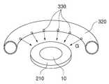
상기 가스 공급부(300)는 상기 웨이퍼 보트(200)를 감싸는 구조로 상기 웨이퍼 보트(200) 둘레를 따라 구비되어 상기 각 웨이퍼(10)의 표면에 반도체 에피 박막을 성장시키도록 외부로부터 상기 반응 챔버(100) 내부로 반응가스(G)를 공급한다. 구체적으로, 상기 가스 공급부(300)는 외부로부터 상기 반응 챔버(100) 내부로 상기 반응가스(G)를 각각 공급하는 복수의 가스관(310) 및 상기 복수의 가스관(310)과 각각 연통하여 각 가스관(310)을 통해 공급되는 상기 반응가스(G)를 분리하여 각 웨이퍼(10)로 분사하는 복수의 분사관(320)을 포함할 수 있다.The
상기 복수의 가스관(310)은 상기 웨이퍼 보트(200)와 상기 내부 챔버(110) 사이에서 상기 웨이퍼 보트(200)에 적재된 상기 복수의 웨이퍼(10)의 적재방향을 따라서 수직하게 연장되어 상기 웨이퍼 보트(200)와 나란히 배치될 수 있다.The plurality of
상기 복수의 가스관(310)은 상기 반응 챔버(100)의 상부로부터 하부를 향해 상기 반응가스(G)를 공급하며, 따라서, 상기 반응가스(G)가 하부까지 균일하게 공급될 수 있도록 한다. 그리고, 각 가스관(310)을 통해 공급되는 상기 반응가스(G)는 동일하거나 서로 다른 종류일 수 있다.The plurality of
상기 반응가스(G)는 질화물 반도체(Ga(Al, In)N)의 합금 형태 및 도핑 소스로 사용되는 것으로 TMGa, TEGa, TMIn, TMAl, SiH4, Cp2Mg, DEZn, NH3, H2, N2 등을 포함할 수 있다. 그리고, 산화물 반도체(Zn(Cd, Mg)O)의 합금 형태 및 도핑 소스로 사용되는 것으로 DMGa, DEZn, Cd[(EPiPr2)2N]2 (E=S, Se), Cp2Mg, N2, Ar, O2, N2O, O3 등을 포함할 수 있다.The reaction gas (G) is a nitride semiconductor to be used as alloy type, and doping the source of the (Ga (Al, In) N ) TMGa, TEGa, TMIn, TMAl, SiH 4, Cp 2 Mg, DEZn, NH 3, H 2 , N2 , and the like. (EPiPr2 )2 N]2 (E = S, Se), Cp2 Mg, and N (N2 O), which are used as the doping source and the alloy type of the oxide semiconductor (Zn (Cd,2 , Ar, O2 , N2 O, O3 , and the like.
도 1, 도4 및 도 5에서 도시하는 바와 같이 상기 복수의 분사관(320)은 상기 복수의 가스관(310)과 각각 연통하여 각 가스관(310)을 통해 공급되는 상기 반응가스(G)를 분리하여 각 웨이퍼(10)로 분사한다. 구체적으로, 상기 복수의 분사관(320)은 상기 웨이퍼 보트(200)를 둘러싸는 링 형상의 구조를 이루며, 상기 적재된 웨이퍼(10)의 개수에 대응하여 복수개가 구비된다. 그리고, 상기 복수의 분사관(320)은 상기 복수의 웨이퍼(10)의 적재간격에 대응하여 상기 웨이퍼 보트(200)를 따라 상하 방향으로 배열된다. 이때, 상기 복수의 분사관(320)은 상기 적재된 웨이퍼(10)와 웨이퍼(10) 사이에 각각 위치하여 각 웨이퍼(10)와 평행하게 배치될 수 있다. 이와 같이, 분사관(320)이 각 웨이퍼(10)에 대응하여 구비됨으로써 각 웨이퍼(10)에 균일하게 반응가스(G)를 분사할 수 있어 개별 웨이퍼간(wafer to wafer) 박막의 균일성을 확보할 수 있는 장점이 있다. 도면에서는 상기 분사관(320)이 원형의 링 형상으로 구비되는 것으로 도시하고 있으나, 이에 한정하는 것은 아니며, 도면으로 도시하지는 않았으나 삼각형, 사각형, 기타 다각형의 링 형상으로 구비되는 것도 가능하다.1, 4, and 5, the plurality of
도 4 및 도 5에서 도시하는 바와 같이, 상기 링 형상의 구조를 이루는 분사관(320)은 서로 분리되어 각각 서로 다른 가스관(310)과 연통하며, 각 가스관(310)을 통해 공급되는 상기 반응가스(G)를 분리해서 각 웨이퍼(10)로 분사한다.As shown in FIGS. 4 and 5, the
구체적으로, 상기 링 형상의 구조를 이루는 분사관(320)은 상기 복수의 가스관(310)과 대응되는 개수로 분리된다. 예를 들어, 도 5에서와 같이, 상기 가스관(310)이 제1 가스관(311) 및 제2 가스관(312)의 2개로 구비되는 경우에는 상기 분사관(320)도 제1 분사관(321) 및 제2 분사관(322)의 2개로 분리되어 구비된다. 이 경우, 상기 분사관(320)은 도 5a에서 도시하는것처럼 제1 분사관(321)과 제2 분사관(322)이 서로 연결되는 구조로 분리될 수 있다. 또한, 도 5b 및 도 5c에서 도시하는것처럼 제1 분사관(321)과 제2 분사관(322)이 일정 간격을 두고 서로 떨어져 배치되는 구조로 분리될 수도 있다.Specifically, the
그리고, 상기 분리된 복수의 분사관(320) 중 일측의 분사관(321)은 상기 복수의 가스관(310) 중 어느 하나의 가스관(311)과 연통하고, 타측의 분사관(322)은 다른 하나의 가스관(312)과 연통한다. 즉, 도면에서와 같이 상기 링 형상의 구조를 이루는 분사관(320) 중 제1 분사관(321)은 제1 가스관(311)과만 연통하고, 상기 제1 분사관(321)과 분리된 제2 분사관(322)은 제2 가스관(312)과만 각각 연통한다. 따라서, 각 가스관(311)을 통해 공급되는 반응가스(G1)는 해당 가스관(311)과 연통하는 분사관(321)을 통해 분사되며, 다른 가스관(312)을 통해 공급되는 반응가스(G2)와는 혼합되지 않고 서로 분리된 상태로 분사된다.One of the plurality of
종래의 경우 싱글 가스관을 통해 반응가스를 공급하였고, 이렇게 공급된 반응가스는 웨이퍼로 분사되기 전에 가스관 내에서 먼저 반응을 일으켜 가스관을 막아버리거나 분사되는 유량이 균일하지 못하는 단점이 있었다. 따라서, 본 발명에 따른 실시예에서와 같이 반응가스(G)가 공급되는 루트를 구분하여 공급하는 한편, 각각의 가스관(310)을 통해 구분되어 공급된 반응가스(G)를 분리된 상태로 분사하는 경우 반응가스(G)가 반응 챔버(100) 내부로 분사되기 전에 서로 혼합되어 반응을 일으키는 기존의 문제를 효과적으로 해결할 수 있다. 또한, 분사되는 반응가스(G)의 유량을 조절하는 것이 용이하다는 장점이 있다.Conventionally, the reaction gas is supplied through a single gas pipe, and the reaction gas thus supplied is firstly reacted in the gas pipe before being injected into the wafer, thereby blocking the gas pipe, or the flow rate of the injected gas is not uniform. Therefore, as in the embodiment of the present invention, the route through which the reaction gas G is supplied is divided and supplied, and the reactive gas G, which is separately supplied through the
상기 분사관(320)은 고온에서 견딜수 있도록 석영, 세라믹, 몰리브덴(Mo), 탄소(C) 등의 재질로 형성될 수 있다.
The
한편, 도 6 및 도 7에서 도시하는 바와 같이, 상기 복수의 분사관(320)은 상기 웨이퍼 보트(200)와 마주하는 내주면을 따라서 복수의 분사노즐(330)을 구비하여 상기 적재된 각 웨이퍼(10)의 중심부를 향해 상기 반응가스(G)를 분사한다.6 and 7, the plurality of jetting
구체적으로, 도 7에서 도시하는 바와 같이, 상기 복수의 분사노즐(330)은 상기 웨이퍼(10)를 향해 소정 기울기(θ)로 하향 경사져 구비될 수 있다. 그리고, 상기 분사노즐(330)의 기울기(θ)는 상기 분사관(320)의 배치 위치에 따라서 다양하게 변경될 수 있다.Specifically, as shown in FIG. 7, the plurality of
10... 웨이퍼100... 반응 챔버
110... 내부 챔버111... 분사홀
120... 외부 챔버130... 게이트부
131... 쓰루홀200... 웨이퍼 보트
210... 홀더220... 홈
300... 가스 공급부310... 가스관
320... 분사관330... 분사노즐10 ...
110 ...
120 ...
131 ... Through
210 ...
300 ...
320 ... jetting
Claims (15)
Translated fromKorean상기 반응 공간 내에 배치되며, 상기 반응 챔버의 높이 방향을 따라 배열되는 복수개의 웨이퍼가 적재되는 웨이퍼 보트; 및
상기 웨이퍼 보트를 감싸는 구조로 상기 웨이퍼 보트 둘레를 따라 구비되어 상기 복수의 웨이퍼 각각에 대해 제1 가스를 분사하는 가스 공급부를 포함하되,
상기 반응 챔버는 상기 웨이퍼 보트 상부에서 상기 복수의 웨이퍼를 향하는 방향으로 상기 제1 가스와 다른 제2 가스를 분사하는 복수의 분사홀 및 상기 웨이퍼 보트의 상부에서 상기 복수의 분사홀을 개폐시켜 상기 복수의 분사홀을 통해 분사되는 상기 제2 가스의 유량을 조절하는 게이트부를 포함하고,
상기 가스 공급부는 외부로부터 상기 반응 챔버 내부로 상기 제1 가스를 각각 공급하는 복수의 가스관과, 상기 복수의 가스관과 각각 연통하여 각 가스관을 통해 공급되는 상기 제1 가스를 분리하여 각 웨이퍼로 분사하는 복수의 분사관을 포함하는 화학 기상 증착 장치.
A reaction chamber having a reaction space;
A wafer boat disposed in the reaction space and loaded with a plurality of wafers arranged along a height direction of the reaction chamber; And
And a gas supply unit disposed along the wafer boat to surround the wafer boat and configured to inject a first gas to each of the plurality of wafers,
Wherein the reaction chamber includes a plurality of injection holes for injecting a second gas different from the first gas in a direction toward the plurality of wafers from the upper portion of the wafer boat and a plurality of injection holes And a gate portion for regulating a flow rate of the second gas injected through the injection hole of the second gas,
Wherein the gas supply unit includes a plurality of gas pipes for respectively supplying the first gas into the reaction chamber from the outside and a plurality of gas pipes communicating with the plurality of gas pipes to separate the first gas supplied through each gas pipe, A chemical vapor deposition apparatus comprising a plurality of spray tubes.
상기 복수의 분사관은 상기 웨이퍼 보트를 둘러싸는 링 형상의 구조를 이루고,
상기 게이트부는 상기 복수의 분사홀과 대응되는 위치의 복수의 쓰루홀을 구비하는 판(plate) 형태이며, 상기 각 분사홀에 대한 상기 쓰루홀의 위치변동을 통해 상기 분사홀의 개폐 정도를 조절하고,
상기 제1 가스는 반응가스를 포함하고,
상기 제2 가스는 분위기 가스를 포함하는 것을 특징으로 하는 화학 기상 증착 장치.
The method according to claim 1,
Wherein the plurality of injection pipes form a ring-shaped structure surrounding the wafer boat,
Wherein the gate unit is in the form of a plate having a plurality of through holes at positions corresponding to the plurality of injection holes and controls the degree of opening and closing of the injection holes through the positional change of the through holes with respect to the respective injection holes,
Wherein the first gas comprises a reactive gas,
Wherein the second gas comprises atmospheric gas.
상기 링 형상의 구조를 이루는 분사관은 서로 분리되어 각각 서로 다른 가스관과 연통하고,
상기 복수의 분사관은 상기 적재된 각 웨이퍼와 평행하게 배치되는 것을 특징으로 하는 화학 기상 증착 장치.
3. The method of claim 2,
The spray tubes constituting the ring-shaped structure are separated from each other to communicate with different gas pipes,
Wherein the plurality of spray tubes are arranged in parallel with each of the stacked wafers.
상기 링 형상의 구조를 이루는 분사관은 상기 복수의 가스관과 대응되는 개수로 분리되며, 상기 분리된 복수의 분사관 중 일측의 분사관은 상기 복수의 가스관 중 어느 하나의 가스관과 연통하고 타측의 분사관은 다른 하나의 가스관과 연통하는 것을 특징으로 하는 화학 기상 증착 장치.
3. The method of claim 2,
Wherein the spray tubes constituting the ring-shaped structure are divided into a number corresponding to the plurality of gas tubes, and one of the plurality of spray tubes is communicated with one of the plurality of gas tubes, And the capillary tube communicates with the other gas pipe.
상기 복수의 분사관은 상기 복수의 웨이퍼의 적재간격에 대응하여 배열되어 상기 적재된 웨이퍼와 웨이퍼 사이에 각각 위치하여 배치되는 것을 특징으로 하는 화학 기상 증착 장치.
5. The method according to any one of claims 1 to 4,
Wherein the plurality of injection tubes are arranged in correspondence with a stacking interval of the plurality of wafers, and are disposed between the stacked wafers and the wafers, respectively.
상기 복수의 분사관은 상기 웨이퍼 보트와 마주하는 내주면을 따라서 복수의 분사노즐을 구비하여 상기 적재된 각 웨이퍼의 중심부를 향해 반응가스를 분사하는 것을 특징으로 하는 화학 기상 증착 장치.
The method according to claim 1,
Wherein the plurality of spray tubes are provided with a plurality of spray nozzles along an inner circumferential surface facing the wafer boat to spray a reaction gas toward a central portion of each of the stacked wafers.
상기 복수의 분사노즐은 상기 웨이퍼를 향해 하향 경사진 것을 특징으로 하는 화학 기상 증착 장치.
The method according to claim 6,
Wherein the plurality of injection nozzles are inclined downward toward the wafer.
상기 반응 챔버는 상기 제2 가스가 상기 반응 공간으로 분사되기 전에 수용되는 수용 공간을 더 포함하고,
상기 수용 공간은 상기 반응 공간, 상기 복수의 분사홀 및 상기 게이트부의 상부에 배치되고,
상기 제2 가스는 상기 복수의 분사홀로부터 상기 반응 공간 내로 샤워링 방식으로 분사되는 것을 특징으로 하는 화학 기상 증착 장치.
The method according to claim 1,
Wherein the reaction chamber further comprises an accommodation space in which the second gas is accommodated before being injected into the reaction space,
Wherein the accommodation space is disposed on the reaction space, the plurality of injection holes, and the gate portion,
Wherein the second gas is injected from the plurality of injection holes into the reaction space in a showering manner.
상기 반응 공간 내에 배치되며, 상기 내부 챔버의 높이 방향으로 복수개의 웨이퍼가 적재되는 웨이퍼 보트;
상기 웨이퍼 보트를 감싸는 구조로 상기 웨이퍼 보트 둘레를 따라 구비되어 상기 복수의 웨이퍼 각각에 대해 제1 가스를 분사하는 가스 공급부;
상기 반응 공간 상부에서 상기 제1 가스와 다른 제2 가스를 상기 복수개의 웨이퍼를 향하는 방향으로 분사하는 복수의 분사홀; 및
상기 복수의 분사홀 상부에서 상기 복수의 분사홀을 개폐시켜 상기 복수의 분사홀을 통해 분사되는 상기 제2 가스의 유량을 조절하는 게이트부를 포함하는 화학 기상 증착 장치.
An inner chamber having a reaction space;
A wafer boat disposed in the reaction space and loaded with a plurality of wafers in a height direction of the inner chamber;
A gas supply unit disposed along the wafer boat to surround the wafer boat and configured to inject a first gas to each of the plurality of wafers;
A plurality of injection holes for spraying a second gas different from the first gas in a direction toward the plurality of wafers at an upper portion of the reaction space; And
And a gate portion for opening and closing the plurality of injection holes at the upper portion of the plurality of injection holes to adjust a flow rate of the second gas injected through the plurality of injection holes.
상기 내부 챔버를 덮는 외부 챔버; 및
상기 내부 챔버와 상기 외부 챔버 사이에 제공되며 상기 반응 공간으로 분사되기 전의 상기 제2 가스를 수용하는 수용 공간을 더 포함하고,
상기 게이트부는 상기 복수의 분사홀과 대응되는 위치에 복수의 쓰루홀을 구비하며, 상기 각 분사홀에 대한 상기 복수의 쓰루홀의 위치변동을 통해 상기 복수의 분사홀의 개폐 정도를 조절하고,
상기 가스 공급부는 상기 반응 공간 내부로 상기 제1 가스를 각각 공급하는 복수의 가스관과, 상기 복수의 가스관과 각각 연통하여 각 가스관을 통해 공급되는 상기 제1 가스를 분리하여 각 웨이퍼로 분사하는 복수의 분사관을 포함하고,
상기 제1 가스는 반응 가스를 포함하고,
상기 제2 가스는 분위기 가스를 포함하는 것을 특징으로 하는 화학 기상 증착 장치.
10. The method of claim 9,
An outer chamber covering the inner chamber; And
Further comprising: an accommodating space provided between the inner chamber and the outer chamber for accommodating the second gas before being injected into the reaction space,
Wherein the gate portion has a plurality of through holes at positions corresponding to the plurality of injection holes and adjusts the degree of opening and closing of the plurality of injection holes through the variation of the positions of the plurality of through holes with respect to the respective injection holes,
Wherein the gas supply unit comprises: a plurality of gas pipes for respectively supplying the first gas into the reaction space; a plurality of gas pipes for separating the first gas supplied through each of the gas pipes, Including a spray tube,
Wherein the first gas comprises a reactive gas,
Wherein the second gas comprises atmospheric gas.
Priority Applications (2)
| Application Number | Priority Date | Filing Date | Title |
|---|---|---|---|
| KR1020110107485AKR101879175B1 (en) | 2011-10-20 | 2011-10-20 | Chemical Vapor Deposition Apparatus |
| US13/655,696US9410247B2 (en) | 2011-10-20 | 2012-10-19 | Chemical vapor deposition apparatus |
Applications Claiming Priority (1)
| Application Number | Priority Date | Filing Date | Title |
|---|---|---|---|
| KR1020110107485AKR101879175B1 (en) | 2011-10-20 | 2011-10-20 | Chemical Vapor Deposition Apparatus |
Publications (2)
| Publication Number | Publication Date |
|---|---|
| KR20130043399A KR20130043399A (en) | 2013-04-30 |
| KR101879175B1true KR101879175B1 (en) | 2018-08-20 |
Family
ID=48134905
Family Applications (1)
| Application Number | Title | Priority Date | Filing Date |
|---|---|---|---|
| KR1020110107485AActiveKR101879175B1 (en) | 2011-10-20 | 2011-10-20 | Chemical Vapor Deposition Apparatus |
Country Status (2)
| Country | Link |
|---|---|
| US (1) | US9410247B2 (en) |
| KR (1) | KR101879175B1 (en) |
Families Citing this family (21)
| Publication number | Priority date | Publication date | Assignee | Title |
|---|---|---|---|---|
| KR101879175B1 (en)* | 2011-10-20 | 2018-08-20 | 삼성전자주식회사 | Chemical Vapor Deposition Apparatus |
| KR101408084B1 (en)* | 2011-11-17 | 2014-07-04 | 주식회사 유진테크 | Apparatus for processing substrate including auxiliary gas supply port |
| KR101364701B1 (en)* | 2011-11-17 | 2014-02-20 | 주식회사 유진테크 | Apparatus for processing substrate with process gas having phase difference |
| US9017763B2 (en)* | 2012-12-14 | 2015-04-28 | Taiwan Semiconductor Manufacturing Company, Ltd. | Injector for forming films respectively on a stack of wafers |
| US10961621B2 (en) | 2015-06-04 | 2021-03-30 | Svagos Technik, Inc. | CVD reactor chamber with resistive heating and substrate holder |
| WO2017040868A1 (en)* | 2015-09-01 | 2017-03-09 | Crystal Solar, Inc. | Cvd reactor chamber with resistive heating |
| KR101760316B1 (en)* | 2015-09-11 | 2017-07-21 | 주식회사 유진테크 | Substrate Processing Apparatus |
| KR102678733B1 (en)* | 2015-12-04 | 2024-06-26 | 어플라이드 머티어리얼스, 인코포레이티드 | Advanced coating methods and materials to prevent HDP-CVD chamber arcing |
| US20180033659A1 (en)* | 2016-07-28 | 2018-02-01 | Applied Materials, Inc. | Gas purge system and method for outgassing control |
| JP6710130B2 (en)* | 2016-09-13 | 2020-06-17 | 東京エレクトロン株式会社 | Substrate processing equipment |
| WO2018154823A1 (en)* | 2017-02-23 | 2018-08-30 | 株式会社Kokusai Electric | Substrate processing device, method of manufacturing semiconductor device, and program |
| US10529543B2 (en)* | 2017-11-15 | 2020-01-07 | Taiwan Semiconductor Manufacturing Co., Ltd. | Etch process with rotatable shower head |
| EP3599290A3 (en) | 2018-07-24 | 2020-06-03 | Lg Electronics Inc. | Chemical vapor deposition equipment for solar cell and deposition method thereof |
| KR102206215B1 (en)* | 2018-12-28 | 2021-01-22 | (주)피앤테크 | Prevention of SiH4 contact to quartz tube used for deposition of wafer |
| KR102315665B1 (en)* | 2019-08-19 | 2021-10-22 | 세메스 주식회사 | Apparatus for treating substrate |
| TWI889744B (en) | 2020-01-29 | 2025-07-11 | 荷蘭商Asm Ip私人控股有限公司 | Contaminant trap system, and baffle plate stack |
| KR102661859B1 (en)* | 2021-04-16 | 2024-04-30 | 주식회사 디스닉스 | Sputtering equipment including ion implantation shower head |
| TW202303865A (en)* | 2021-05-28 | 2023-01-16 | 荷蘭商Asm Ip私人控股有限公司 | Contaminant trap system, and baffle plate stack |
| KR102359846B1 (en)* | 2021-08-13 | 2022-02-09 | (주)피앤테크 | Gas furnishing device for homogeneous gas furnishing into the chamber of deposition equipment |
| US11769659B2 (en)* | 2021-08-27 | 2023-09-26 | Taiwan Semiconductor Manufacturing Company, Ltd. | Showerhead assembly and method of servicing assembly for semiconductor manufacturing |
| TW202526081A (en)* | 2023-09-26 | 2025-07-01 | 荷蘭商Asm Ip私人控股有限公司 | Gas injector, and apparatus to process substrate |
Family Cites Families (70)
| Publication number | Priority date | Publication date | Assignee | Title |
|---|---|---|---|---|
| JPS61222534A (en)* | 1985-03-28 | 1986-10-03 | Anelva Corp | Method and apparatus for surface treatment |
| US5376628A (en)* | 1988-06-30 | 1994-12-27 | Anelva Corporation | Method of improving or producing oxide superconductor |
| JP2654996B2 (en)* | 1988-08-17 | 1997-09-17 | 東京エレクトロン株式会社 | Vertical heat treatment equipment |
| JPH02114530A (en)* | 1988-10-25 | 1990-04-26 | Mitsubishi Electric Corp | Thin film forming equipment |
| US5429070A (en)* | 1989-06-13 | 1995-07-04 | Plasma & Materials Technologies, Inc. | High density plasma deposition and etching apparatus |
| US5279670A (en)* | 1990-03-31 | 1994-01-18 | Tokyo Electron Sagami Limited | Vertical type diffusion apparatus |
| JPH05217929A (en)* | 1992-01-31 | 1993-08-27 | Tokyo Electron Tohoku Kk | Oxidation diffusion treating apparatus |
| TW239164B (en)* | 1992-08-12 | 1995-01-21 | Tokyo Electron Co Ltd | |
| JP3125199B2 (en)* | 1993-03-18 | 2001-01-15 | 東京エレクトロン株式会社 | Vertical heat treatment equipment |
| US5592581A (en)* | 1993-07-19 | 1997-01-07 | Tokyo Electron Kabushiki Kaisha | Heat treatment apparatus |
| JP3024449B2 (en)* | 1993-07-24 | 2000-03-21 | ヤマハ株式会社 | Vertical heat treatment furnace and heat treatment method |
| US5614055A (en)* | 1993-08-27 | 1997-03-25 | Applied Materials, Inc. | High density plasma CVD and etching reactor |
| JPH07130662A (en)* | 1993-11-04 | 1995-05-19 | Nec Corp | Vertical low pressure cvd apparatus |
| US5525159A (en)* | 1993-12-17 | 1996-06-11 | Tokyo Electron Limited | Plasma process apparatus |
| US5620523A (en)* | 1994-04-11 | 1997-04-15 | Canon Sales Co., Inc. | Apparatus for forming film |
| US5522934A (en)* | 1994-04-26 | 1996-06-04 | Tokyo Electron Limited | Plasma processing apparatus using vertical gas inlets one on top of another |
| JP3699142B2 (en)* | 1994-09-30 | 2005-09-28 | アネルバ株式会社 | Thin film forming equipment |
| JPH08264521A (en)* | 1995-03-20 | 1996-10-11 | Kokusai Electric Co Ltd | Reactor for semiconductor manufacturing |
| JPH0955372A (en)* | 1995-08-11 | 1997-02-25 | Nippon Steel Corp | Plasma processing device |
| CA2205817C (en)* | 1996-05-24 | 2004-04-06 | Sekisui Chemical Co., Ltd. | Treatment method in glow-discharge plasma and apparatus thereof |
| WO1998000576A1 (en)* | 1996-06-28 | 1998-01-08 | Lam Research Corporation | Apparatus and method for high density plasma chemical vapor deposition |
| US6013155A (en)* | 1996-06-28 | 2000-01-11 | Lam Research Corporation | Gas injection system for plasma processing |
| JP3270730B2 (en)* | 1997-03-21 | 2002-04-02 | 株式会社日立国際電気 | Substrate processing apparatus and substrate processing method |
| JP3164019B2 (en)* | 1997-05-21 | 2001-05-08 | 日本電気株式会社 | Silicon oxide film, method for forming the same, and film forming apparatus |
| US6706334B1 (en)* | 1997-06-04 | 2004-03-16 | Tokyo Electron Limited | Processing method and apparatus for removing oxide film |
| JP2973971B2 (en)* | 1997-06-05 | 1999-11-08 | 日本電気株式会社 | Heat treatment apparatus and thin film forming method |
| US6042687A (en)* | 1997-06-30 | 2000-03-28 | Lam Research Corporation | Method and apparatus for improving etch and deposition uniformity in plasma semiconductor processing |
| US6204194B1 (en)* | 1998-01-16 | 2001-03-20 | F.T.L. Co., Ltd. | Method and apparatus for producing a semiconductor device |
| US6132552A (en)* | 1998-02-19 | 2000-10-17 | Micron Technology, Inc. | Method and apparatus for controlling the temperature of a gas distribution plate in a process reactor |
| KR20000002834A (en)* | 1998-06-23 | 2000-01-15 | 윤종용 | Diffusion equipment and control method for semiconductor manufacture forming air curtain |
| US6365016B1 (en)* | 1999-03-17 | 2002-04-02 | General Electric Company | Method and apparatus for arc plasma deposition with evaporation of reagents |
| JP4045689B2 (en)* | 1999-04-14 | 2008-02-13 | 東京エレクトロン株式会社 | Heat treatment equipment |
| EP1115147A4 (en)* | 1999-05-26 | 2007-05-02 | Tadahiro Ohmi | PLASMA TREATMENT DEVICE |
| KR20010062209A (en)* | 1999-12-10 | 2001-07-07 | 히가시 데쓰로 | Processing apparatus with a chamber having therein a high-etching resistant sprayed film |
| KR100458982B1 (en)* | 2000-08-09 | 2004-12-03 | 주성엔지니어링(주) | Semiconductor device fabrication apparatus having rotatable gas injector and thin film deposition method using the same |
| US7246796B2 (en)* | 2001-01-18 | 2007-07-24 | Masayuki Toda | Carburetor, various types of devices using the carburetor, and method of vaporization |
| CN1229855C (en)* | 2001-03-28 | 2005-11-30 | 大见忠弘 | Plasma treatment device |
| KR20020092119A (en) | 2001-06-02 | 2002-12-11 | 삼성전자 주식회사 | Horizontal type gas injection nozzle |
| KR20020095842A (en)* | 2001-06-16 | 2002-12-28 | 삼성전자 주식회사 | Ashing apparatus of semiconductor |
| KR100400044B1 (en)* | 2001-07-16 | 2003-09-29 | 삼성전자주식회사 | Shower head of wafer treatment apparatus having gap controller |
| US7578883B1 (en)* | 2001-08-29 | 2009-08-25 | Lsi Corporation | Arrangement and method for abating effluent from a process |
| KR100450068B1 (en)* | 2001-11-23 | 2004-09-24 | 주성엔지니어링(주) | Multi-sectored flat board type showerhead used in CVD apparatus |
| US6972055B2 (en)* | 2003-03-28 | 2005-12-06 | Finens Corporation | Continuous flow deposition system |
| KR100766196B1 (en) | 2003-08-26 | 2007-10-10 | 가부시키가이샤 히다치 고쿠사이 덴키 | Method for manufacturing semiconductor device and substrate processing apparatus |
| JP4273932B2 (en)* | 2003-11-07 | 2009-06-03 | 株式会社島津製作所 | Surface wave excitation plasma CVD equipment |
| JP4179311B2 (en)* | 2004-07-28 | 2008-11-12 | 東京エレクトロン株式会社 | Film forming method, film forming apparatus, and storage medium |
| KR100609065B1 (en)* | 2004-08-04 | 2006-08-10 | 삼성전자주식회사 | Oxide film forming apparatus and method |
| DE102005045081B4 (en)* | 2004-09-29 | 2011-07-07 | Covalent Materials Corp. | susceptor |
| JP2006179770A (en)* | 2004-12-24 | 2006-07-06 | Watanabe Shoko:Kk | Substrate surface processing apparatus |
| KR20060075552A (en)* | 2004-12-28 | 2006-07-04 | 동부일렉트로닉스 주식회사 | Chemical vapor deposition apparatus |
| JP4698354B2 (en)* | 2005-09-15 | 2011-06-08 | 株式会社リコー | CVD equipment |
| KR101047230B1 (en)* | 2006-03-28 | 2011-07-06 | 가부시키가이샤 히다치 고쿠사이 덴키 | Substrate treating apparatus |
| JP5023646B2 (en)* | 2006-10-10 | 2012-09-12 | 東京エレクトロン株式会社 | Exhaust system, collection unit, and processing apparatus using the same |
| US20080173238A1 (en)* | 2006-12-12 | 2008-07-24 | Hitachi Kokusai Electric Inc. | Substrate processing apparatus, method of manufacturing semiconductor device, and reaction vessel |
| US7967996B2 (en)* | 2007-01-30 | 2011-06-28 | Applied Materials, Inc. | Process for wafer backside polymer removal and wafer front side photoresist removal |
| KR20090009572A (en) | 2007-07-20 | 2009-01-23 | 국제엘렉트릭코리아 주식회사 | Furnace Semiconductor Equipment |
| KR20090016924A (en)* | 2007-08-13 | 2009-02-18 | 국제엘렉트릭코리아 주식회사 | Furnace Semiconductor Equipment |
| US8329593B2 (en)* | 2007-12-12 | 2012-12-11 | Applied Materials, Inc. | Method and apparatus for removing polymer from the wafer backside and edge |
| KR100998011B1 (en)* | 2008-05-22 | 2010-12-03 | 삼성엘이디 주식회사 | Chemical Vapor Deposition Equipment |
| JP2010141223A (en)* | 2008-12-15 | 2010-06-24 | Hitachi Kokusai Electric Inc | Method of manufacturing semiconductor device and substrate processing apparatus |
| JP5658463B2 (en)* | 2009-02-27 | 2015-01-28 | 株式会社日立国際電気 | Substrate processing apparatus and semiconductor device manufacturing method |
| JP5730496B2 (en)* | 2009-05-01 | 2015-06-10 | 株式会社日立国際電気 | Heat treatment apparatus, semiconductor device manufacturing method, and substrate processing method |
| JP5136574B2 (en)* | 2009-05-01 | 2013-02-06 | 東京エレクトロン株式会社 | Plasma processing apparatus and plasma processing method |
| KR101101964B1 (en) | 2009-06-29 | 2012-01-02 | (주)울텍 | Low pressure chemical vapor deposition apparatus using plasma |
| US8872142B2 (en)* | 2010-03-18 | 2014-10-28 | Gigaphoton Inc. | Extreme ultraviolet light generation apparatus |
| JP5243519B2 (en)* | 2010-12-22 | 2013-07-24 | 東京エレクトロン株式会社 | Deposition equipment |
| JP2012195565A (en)* | 2011-02-28 | 2012-10-11 | Hitachi Kokusai Electric Inc | Substrate processing apparatus, substrate processing method, and manufacturing method of semiconductor device |
| US9303318B2 (en)* | 2011-10-20 | 2016-04-05 | Applied Materials, Inc. | Multiple complementary gas distribution assemblies |
| KR101879175B1 (en)* | 2011-10-20 | 2018-08-20 | 삼성전자주식회사 | Chemical Vapor Deposition Apparatus |
| US20140166618A1 (en)* | 2012-12-14 | 2014-06-19 | The Penn State Research Foundation | Ultra-high speed anisotropic reactive ion etching |
- 2011
- 2011-10-20KRKR1020110107485Apatent/KR101879175B1/enactiveActive
- 2012
- 2012-10-19USUS13/655,696patent/US9410247B2/enactiveActive
Also Published As
| Publication number | Publication date |
|---|---|
| KR20130043399A (en) | 2013-04-30 |
| US20130098293A1 (en) | 2013-04-25 |
| US9410247B2 (en) | 2016-08-09 |
Similar Documents
| Publication | Publication Date | Title |
|---|---|---|
| KR101879175B1 (en) | Chemical Vapor Deposition Apparatus | |
| KR101598911B1 (en) | Vapor phase growing apparatus and vapor phase growing method | |
| KR101699815B1 (en) | Vapor phase growing apparatus | |
| KR102025717B1 (en) | Chemical vapor deposition apparatus and method of manufacturing led using the same | |
| KR101715193B1 (en) | Apparatus for processing substrate | |
| US10130958B2 (en) | Showerhead assembly with gas injection distribution devices | |
| CN103098175B (en) | Sprinkler assembly with gas injection distribution device | |
| CN102656665B (en) | Vapor phase growth apparatus, vapor phase growth method, and manufacturing method of semiconductor element | |
| TWI499085B (en) | Growth of group iii-v material layers by spatially confined epitaxy | |
| KR101759649B1 (en) | Chemical Vapor Deposition Apparatus and Method of Forming Semiconductor Superlattice Structure Using The Same | |
| KR101205436B1 (en) | Chemical Vapor Deposition Apparatus | |
| CN105442039A (en) | Graphite disc for accommodating silicon substrate for MOCVD (metal-organic chemical vapor deposition) | |
| US20100126419A1 (en) | Susceptor for cvd apparatus and cvd apparatus including the same | |
| JP2011222592A (en) | Vapor phase deposition apparatus and vapor phase deposition method | |
| US20150000596A1 (en) | Mocvd gas diffusion system with gas inlet baffles | |
| TWI682429B (en) | Substrate processing apparatus | |
| CN102031498A (en) | Substrate support seat for III-V group thin film growth reaction chamber, reaction chamber thereof and process treatment method | |
| WO2012040505A2 (en) | Processing systems and apparatuses having a shaft cover | |
| KR20140102880A (en) | Method of manufacturing a semiconductor light emitting device and chemical vapor deposition apparatus | |
| KR20150101236A (en) | Modular Chemical Vapor Deposition individually controlling supply gas | |
| CN205313713U (en) | Be used for placing graphite plate of silicon substrate among MOCVD | |
| WO2014012237A1 (en) | Method and apparatus for growing nitride-based compound semiconductor crystals | |
| US20150240358A1 (en) | Susceptor and chemical vapor deposition apparatus having the same | |
| KR102234386B1 (en) | Susceptor and apparatus for chemical vapor deposition using the same | |
| KR20140089167A (en) | Apparatus for processing substrate |
Legal Events
| Date | Code | Title | Description |
|---|---|---|---|
| PA0109 | Patent application | Patent event code:PA01091R01D Comment text:Patent Application Patent event date:20111020 | |
| N231 | Notification of change of applicant | ||
| PN2301 | Change of applicant | Patent event date:20120629 Comment text:Notification of Change of Applicant Patent event code:PN23011R01D | |
| PG1501 | Laying open of application | ||
| A201 | Request for examination | ||
| PA0201 | Request for examination | Patent event code:PA02012R01D Patent event date:20161020 Comment text:Request for Examination of Application Patent event code:PA02011R01I Patent event date:20111020 Comment text:Patent Application | |
| PE0902 | Notice of grounds for rejection | Comment text:Notification of reason for refusal Patent event date:20171215 Patent event code:PE09021S01D | |
| E701 | Decision to grant or registration of patent right | ||
| PE0701 | Decision of registration | Patent event code:PE07011S01D Comment text:Decision to Grant Registration Patent event date:20180629 | |
| GRNT | Written decision to grant | ||
| PR0701 | Registration of establishment | Comment text:Registration of Establishment Patent event date:20180711 Patent event code:PR07011E01D | |
| PR1002 | Payment of registration fee | Payment date:20180712 End annual number:3 Start annual number:1 | |
| PG1601 | Publication of registration | ||
| PR1001 | Payment of annual fee | Payment date:20210628 Start annual number:4 End annual number:4 | |
| PR1001 | Payment of annual fee | Payment date:20220622 Start annual number:5 End annual number:5 | |
| PR1001 | Payment of annual fee | Payment date:20230621 Start annual number:6 End annual number:6 | |
| PR1001 | Payment of annual fee | Payment date:20240626 Start annual number:7 End annual number:7 | |
| PR1001 | Payment of annual fee | Payment date:20250624 Start annual number:8 End annual number:8 |