KR101876011B1 - Oxide thin film transistor and method of manufacturing the same - Google Patents
Oxide thin film transistor and method of manufacturing the sameDownload PDFInfo
- Publication number
- KR101876011B1 KR101876011B1KR1020160011195AKR20160011195AKR101876011B1KR 101876011 B1KR101876011 B1KR 101876011B1KR 1020160011195 AKR1020160011195 AKR 1020160011195AKR 20160011195 AKR20160011195 AKR 20160011195AKR 101876011 B1KR101876011 B1KR 101876011B1
- Authority
- KR
- South Korea
- Prior art keywords
- layer
- thin film
- film transistor
- oxide thin
- oxide
- Prior art date
- Legal status (The legal status is an assumption and is not a legal conclusion. Google has not performed a legal analysis and makes no representation as to the accuracy of the status listed.)
- Expired - Fee Related
Links
Images


Classifications
- H01L29/7869—
- H—ELECTRICITY
- H01—ELECTRIC ELEMENTS
- H01L—SEMICONDUCTOR DEVICES NOT COVERED BY CLASS H10
- H01L21/00—Processes or apparatus adapted for the manufacture or treatment of semiconductor or solid state devices or of parts thereof
- H01L21/02—Manufacture or treatment of semiconductor devices or of parts thereof
- H01L21/02104—Forming layers
- H01L21/02107—Forming insulating materials on a substrate
- H01L21/02109—Forming insulating materials on a substrate characterised by the type of layer, e.g. type of material, porous/non-porous, pre-cursors, mixtures or laminates
- H—ELECTRICITY
- H01—ELECTRIC ELEMENTS
- H01L—SEMICONDUCTOR DEVICES NOT COVERED BY CLASS H10
- H01L21/00—Processes or apparatus adapted for the manufacture or treatment of semiconductor or solid state devices or of parts thereof
- H01L21/02—Manufacture or treatment of semiconductor devices or of parts thereof
- H01L21/02104—Forming layers
- H01L21/02107—Forming insulating materials on a substrate
- H01L21/02225—Forming insulating materials on a substrate characterised by the process for the formation of the insulating layer
- H01L21/0226—Forming insulating materials on a substrate characterised by the process for the formation of the insulating layer formation by a deposition process
- H01L21/02263—Forming insulating materials on a substrate characterised by the process for the formation of the insulating layer formation by a deposition process deposition from the gas or vapour phase
- H01L21/02271—Forming insulating materials on a substrate characterised by the process for the formation of the insulating layer formation by a deposition process deposition from the gas or vapour phase deposition by decomposition or reaction of gaseous or vapour phase compounds, i.e. chemical vapour deposition
- H01L21/0228—Forming insulating materials on a substrate characterised by the process for the formation of the insulating layer formation by a deposition process deposition from the gas or vapour phase deposition by decomposition or reaction of gaseous or vapour phase compounds, i.e. chemical vapour deposition deposition by cyclic CVD, e.g. ALD, ALE, pulsed CVD
- H—ELECTRICITY
- H01—ELECTRIC ELEMENTS
- H01L—SEMICONDUCTOR DEVICES NOT COVERED BY CLASS H10
- H01L21/00—Processes or apparatus adapted for the manufacture or treatment of semiconductor or solid state devices or of parts thereof
- H01L21/02—Manufacture or treatment of semiconductor devices or of parts thereof
- H01L21/04—Manufacture or treatment of semiconductor devices or of parts thereof the devices having potential barriers, e.g. a PN junction, depletion layer or carrier concentration layer
- H01L21/18—Manufacture or treatment of semiconductor devices or of parts thereof the devices having potential barriers, e.g. a PN junction, depletion layer or carrier concentration layer the devices having semiconductor bodies comprising elements of Group IV of the Periodic Table or AIIIBV compounds with or without impurities, e.g. doping materials
- H01L21/28—Manufacture of electrodes on semiconductor bodies using processes or apparatus not provided for in groups H01L21/20 - H01L21/268
- H01L21/28008—Making conductor-insulator-semiconductor electrodes
- H01L21/28017—Making conductor-insulator-semiconductor electrodes the insulator being formed after the semiconductor body, the semiconductor being silicon
- H01L21/28158—Making the insulator
- H01L21/28167—Making the insulator on single crystalline silicon, e.g. using a liquid, i.e. chemical oxidation
- H01L21/28194—Making the insulator on single crystalline silicon, e.g. using a liquid, i.e. chemical oxidation by deposition, e.g. evaporation, ALD, CVD, sputtering, laser deposition
- H—ELECTRICITY
- H01—ELECTRIC ELEMENTS
- H01L—SEMICONDUCTOR DEVICES NOT COVERED BY CLASS H10
- H01L21/00—Processes or apparatus adapted for the manufacture or treatment of semiconductor or solid state devices or of parts thereof
- H01L21/02—Manufacture or treatment of semiconductor devices or of parts thereof
- H01L21/04—Manufacture or treatment of semiconductor devices or of parts thereof the devices having potential barriers, e.g. a PN junction, depletion layer or carrier concentration layer
- H01L21/18—Manufacture or treatment of semiconductor devices or of parts thereof the devices having potential barriers, e.g. a PN junction, depletion layer or carrier concentration layer the devices having semiconductor bodies comprising elements of Group IV of the Periodic Table or AIIIBV compounds with or without impurities, e.g. doping materials
- H01L21/28—Manufacture of electrodes on semiconductor bodies using processes or apparatus not provided for in groups H01L21/20 - H01L21/268
- H01L21/28008—Making conductor-insulator-semiconductor electrodes
- H01L21/28017—Making conductor-insulator-semiconductor electrodes the insulator being formed after the semiconductor body, the semiconductor being silicon
- H01L21/28247—Making conductor-insulator-semiconductor electrodes the insulator being formed after the semiconductor body, the semiconductor being silicon passivation or protection of the electrode, e.g. using re-oxidation
- H—ELECTRICITY
- H01—ELECTRIC ELEMENTS
- H01L—SEMICONDUCTOR DEVICES NOT COVERED BY CLASS H10
- H01L21/00—Processes or apparatus adapted for the manufacture or treatment of semiconductor or solid state devices or of parts thereof
- H01L21/02—Manufacture or treatment of semiconductor devices or of parts thereof
- H01L21/04—Manufacture or treatment of semiconductor devices or of parts thereof the devices having potential barriers, e.g. a PN junction, depletion layer or carrier concentration layer
- H01L21/18—Manufacture or treatment of semiconductor devices or of parts thereof the devices having potential barriers, e.g. a PN junction, depletion layer or carrier concentration layer the devices having semiconductor bodies comprising elements of Group IV of the Periodic Table or AIIIBV compounds with or without impurities, e.g. doping materials
- H01L21/30—Treatment of semiconductor bodies using processes or apparatus not provided for in groups H01L21/20 - H01L21/26
- H01L21/324—Thermal treatment for modifying the properties of semiconductor bodies, e.g. annealing, sintering
- H01L29/66742—
- H01L29/66878—
- H—ELECTRICITY
- H01—ELECTRIC ELEMENTS
- H01L—SEMICONDUCTOR DEVICES NOT COVERED BY CLASS H10
- H01L2924/00—Indexing scheme for arrangements or methods for connecting or disconnecting semiconductor or solid-state bodies as covered by H01L24/00
- H01L2924/10—Details of semiconductor or other solid state devices to be connected
- H01L2924/11—Device type
- H01L2924/13—Discrete devices, e.g. 3 terminal devices
- H01L2924/1304—Transistor
- H01L2924/1306—Field-effect transistor [FET]
- H01L2924/13069—Thin film transistor [TFT]
Landscapes
- Engineering & Computer Science (AREA)
- Manufacturing & Machinery (AREA)
- Physics & Mathematics (AREA)
- Condensed Matter Physics & Semiconductors (AREA)
- General Physics & Mathematics (AREA)
- Computer Hardware Design (AREA)
- Microelectronics & Electronic Packaging (AREA)
- Power Engineering (AREA)
- Chemical Kinetics & Catalysis (AREA)
- Chemical & Material Sciences (AREA)
- Crystallography & Structural Chemistry (AREA)
- General Chemical & Material Sciences (AREA)
- Thin Film Transistor (AREA)
Abstract
Translated fromKoreanDescription
Translated fromKorean본 발명은 산화물 박막 트랜지스터 및 그 제조방법에 관한 것으로, 보다 상세하게는 산화물 박막 트랜지스터를 어닐링 처리하여 안정성을 개선시킨 산화물 박막 트랜지스터 및 그 제조방법에 관한 것이다.The present invention relates to an oxide thin film transistor and a manufacturing method thereof, and more particularly, to an oxide thin film transistor having improved stability by annealing an oxide thin film transistor and a manufacturing method thereof.
FPD(Flat panel display)는 매우 얇고 가벼운 장점으로 디스플레이 시장에서 매우 높은 점유율을 차지하고 있다. FPD는 시장 점유율의 증가와 더불어 대면적화 및 고화질이 요구되고, 나아가 더 가볍고 얇으면서 휘거나 접을 수 있는 플렉서블(flexible) 디스플레이에 적용하기 위해 저온에서 공정이 가능하면서 전기적, 기계적 특성이 우수하고 동작 안정성이 보장되는 백플레인(backplane) 기술이 요구되고 있다.Flat panel displays (FPDs) are very thin and lightweight and occupy a very high share in the display market. FPD is required to be large-sized and high-quality with the increase of market share. Furthermore, it can be processed at low temperature for application to a lighter, thinner and warped or foldable flexible display, and has excellent electrical and mechanical characteristics. Backplane technology is required.
디스플레이의 백플레인으로 사용되는 스위칭 소자나 구동 소자로 비정질 실리콘(a-Si)이나 폴리 실리콘(poly-Si)을 사용하는 실리콘(Si) 기반 박막 트랜지스터(TFT: Thin Film Transistor)와 산화물 반도체 박막 트랜지스터가 있다.Silicon (Si) -based thin film transistors (TFTs) and oxide semiconductor thin film transistors (TFTs) using amorphous silicon (a-Si) or polysilicon have.
실리콘(Si) 기반 박막 트랜지스터의 비정질 실리콘(a-Si) 박막 트랜지스터는 제조가 용이하지만 낮은 전자 이동도를 갖고 있다. 한편, 폴리 실리콘(poly-Si) 박막 트랜지스터는 비정질 실리콘(a-Si) 박막 트랜지스터에 비해 전자 이동도가 높아 대면적의 고화질 디스플레이에 적용가능하며 안정성도 높지만, 제조공정이 복잡하고 제조원가가 높으며, 패널 내 소자 특성의 불균일로 인해 보상회로를 필요로 하는 문제점이 있다.The amorphous silicon (a-Si) thin film transistor of a silicon (Si) based thin film transistor is easy to manufacture but has low electron mobility. On the other hand, a poly-Si thin film transistor has a higher electron mobility than an amorphous silicon (a-Si) thin film transistor and is applicable to a large-area high-quality display and has high stability. However, the manufacturing process is complicated, There is a problem that a compensation circuit is required due to non-uniformity of device characteristics in the panel.
이러한 실리콘(Si) 기반 박막 트랜지스터의 단점을 해결하고자 산화물 반도체 박막 트랜지스터(Oxide TFT)가 개발되고 있다.An oxide semiconductor thin film transistor (Oxide TFT) is being developed to overcome the shortcomings of such a silicon (Si) based thin film transistor.
산화물 박막 트랜지스터는 대면적, 고해상도 디스플레이 구현을 가능하게 할 뿐 아니라 무안경 3D TV로의 적용도 가능하고, 산화물은 저온 공정이 가능하여 플라스틱 기판을 활용한 플렉시블 디스플레이 구현에도 적합한 소재이다. 또한, 에너지 밴드갭이 보통 3 eV 이상 크기 때문에 투명디스플레이에 응용 가능한 차세대 트랜지스터로 많은 주목을 받고 있다.The oxide thin film transistor not only enables realization of a large-area and high-resolution display but also can be applied to a non-spectacled 3D TV, and oxide is a material suitable for realizing a flexible display using a plastic substrate because a low temperature process is possible. In addition, since the energy band gap is usually larger than 3 eV, it is attracting much attention as a next generation transistor applicable to a transparent display.
그 중에서도, 인듐, 갈륨, 아연 및 산소를 구성 원소로 하는 비정질 In-Ga-Zn-O계 재료(이하, 'a-IGZO'라고도 한다)를 사용한 박막 트랜지스터는 온/오프비를 높일 수 있어 유망시 되고 있다.Among them, a thin film transistor using an amorphous In-Ga-Zn-O-based material (hereinafter also referred to as "a-IGZO") having indium, gallium, zinc and oxygen as constituent elements can increase the on / off ratio, Time.
본 발명의 실시예는 산화물 반도체로 구성되는 활성층 및 상기 활성층을 보호하는 패시베이션층을 포함하는 산화물 박막 트랜지스터 및 그 제조방법을 제공하고자 한다.An embodiment of the present invention is to provide an oxide thin film transistor including an active layer made of an oxide semiconductor and a passivation layer protecting the active layer and a method of manufacturing the same.
본 발명의 실시예는 어닐링 처리된 산화물 박막 트랜지스터 및 그 제조방법을 제공하고자 한다.An embodiment of the present invention is to provide an annealed oxide thin film transistor and a method of manufacturing the same.
본 발명의 실시예는 빛에 대한 안정성이 개선된 산화물 박막 트랜지스터 및 그 제조방법을 제공하고자 한다.Embodiments of the present invention provide an oxide thin film transistor having improved stability to light and a method of manufacturing the same.
본 발명의 실시예에 따른 산화물 박막 트랜지스터는 산화물 반도체로 구성되는 활성층 및 상기 활성층을 보호하는 패시베이션층을 포함하는 산화물 박막 트랜지스터에 있어서, 상기 패시베이션층은 산소 전구체로서 오존(O3)을 이용한 원자층 증착법(ALD)을 통하여 상기 활성층 상에 형성되고, 상기 산화물 박막 트랜지스터는 어닐링 처리되는 것을 특징으로 한다.Oxide thin film transistor according to an embodiment of the present invention is an oxide thin film transistor including a passivation layer for protecting the active layer and the active layer consisting of an oxide semiconductor, wherein the passivation layer has an atomic layer using ozone (O3) as an oxygen precursor Is formed on the active layer through a deposition method (ALD), and the oxide thin film transistor is annealed.
상기 어닐링 처리는 100℃ 내지 400℃ 범위의 온도에서 수행될 수 있다.The annealing treatment may be performed at a temperature ranging from 100 ° C to 400 ° C.
또한, 상기 어닐링 처리는 10분 내지 5시간 동안 수행될 수 있다.Further, the annealing treatment may be performed for 10 minutes to 5 hours.
상기 패시베이션층은 5 ㎚ 내지 100 ㎚ 범위의 두께를 가질 수 있다.The passivation layer may have a thickness ranging from 5 nm to 100 nm.
상기 패시베이션층은 Y2O3로 이루어질 수 있다.The passivation layer may be made of Y2 O3 .
상기 활성층은 IGZO로 이루어질 수 있다.The active layer may be made of IGZO.
본 발명의 실시예에 따르면 산화물 반도체로 구성되는 활성층 및 상기 활성층을 보호하는 패시베이션층을 포함하는 산화물 박막 트랜지스터를 제조할 수 있다.According to an embodiment of the present invention, an oxide thin film transistor including an active layer made of an oxide semiconductor and a passivation layer protecting the active layer can be manufactured.
본 발명의 실시예에 따르면 산화물 박막 트랜지스터에 어닐링 처리를 수행하여 빛에 대한 안정성이 개선된 산화물 박막 트랜지스터를 제조할 수 있다.According to an embodiment of the present invention, an oxide thin film transistor having improved stability to light can be manufactured by performing an annealing process on the oxide thin film transistor.
도 1은 본 발명의 일 실시예에 따른 상부 게이트 산화물 박막 트랜지스터의 개략적인 단면도이다.
도 2는 본 발명의 다른 일 실시예에 따른 하부 게이트 산화물 박막 트랜지스터의 개략적인 단면도이다.
도 3 및 도 4는 어닐링 처리되지 않은 산화물 박막 트랜지스터의 전기적 특성을 나타내는 그래프이다.
도 5 및 도 6은 본 발명의 일 실시예에 따라 어닐링 처리된 산화물 박막 트랜지스터의 전기적 특성을 나타내는 그래프이다.1 is a schematic cross-sectional view of a top gate oxide thin film transistor according to an embodiment of the present invention.
2 is a schematic cross-sectional view of a bottom gate oxide thin film transistor according to another embodiment of the present invention.
FIGS. 3 and 4 are graphs showing the electrical characteristics of the non-annealed oxide thin film transistor.
5 and 6 are graphs showing electrical characteristics of an oxide thin film transistor annealed according to an embodiment of the present invention.
이하 첨부 도면들 및 첨부 도면들에 기재된 내용들을 참조하여 본 발명의 실시예를 상세하게 설명하지만, 본 발명이 실시예에 의해 제한되거나 한정되는 것은 아니다.Hereinafter, embodiments of the present invention will be described in detail with reference to the accompanying drawings and accompanying drawings, but the present invention is not limited to or limited by the embodiments.
본 명세서에서 사용된 용어는 실시예들을 설명하기 위한 것이며 본 발명을 제한하고자 하는 것은 아니다. 본 명세서에서, 단수형은 문구에서 특별히 언급하지 않는 한 복수형도 포함한다. 명세서에서 사용되는 "포함한다(comprises)" 및/또는 "포함하는(comprising)"은 언급된 구성요소, 단계, 동작 및/또는 소자는 하나 이상의 다른 구성요소, 단계, 동작 및/또는 소자의 존재 또는 추가를 배제하지 않는다.The terminology used herein is for the purpose of illustrating embodiments and is not intended to be limiting of the present invention. In the present specification, the singular form includes plural forms unless otherwise specified in the specification. It is noted that the terms "comprises" and / or "comprising" used in the specification are intended to be inclusive in a manner similar to the components, steps, operations, and / Or additions.
본 명세서에서 사용되는 "실시예", "예", "측면", "예시" 등은 기술된 임의의 양상(aspect) 또는 설계가 다른 양상 또는 설계들보다 양호하다거나, 이점이 있는 것으로 해석되어야 하는 것은 아니다.As used herein, the terms "embodiment," "example," "side," "example," and the like should be construed as advantageous or advantageous over any other aspect or design It does not.
또한, '또는' 이라는 용어는 배타적 논리합 'exclusive or'이기보다는 포함적인 논리합 'inclusive or'를 의미한다. 즉, 달리 언급되지 않는 한 또는 문맥으로부터 명확하지 않는 한, 'x가 a 또는 b를 이용한다'라는 표현은 포함적인 자연 순열들(natural inclusive permutations) 중 어느 하나를 의미한다.Also, the term 'or' implies an inclusive or 'inclusive' rather than an exclusive or 'exclusive'. That is, unless expressly stated otherwise or clear from the context, the expression 'x uses a or b' means any of the natural inclusive permutations.
또한, 본 명세서 및 청구항들에서 사용되는 단수 표현("a" 또는 "an")은, 달리 언급하지 않는 한 또는 단수 형태에 관한 것이라고 문맥으로부터 명확하지 않는 한, 일반적으로 "하나 이상"을 의미하는 것으로 해석되어야 한다.Also, the phrase "a" or "an ", as used in the specification and claims, unless the context clearly dictates otherwise, or to the singular form, .
또한, 막, 층, 영역, 구성 요청 등의 부분이 다른 부분 "위에" 또는 "상에" 있다고 할 때, 다른 부분의 바로 위에 있는 경우뿐만 아니라, 그 중간에 다른 막, 층, 영역, 구성 요소 등이 개재되어 있는 경우도 포함한다.It will also be understood that when an element such as a film, layer, region, configuration request, etc. is referred to as being "on" or "on" another element, And the like are included.
본 발명의 실시예에 따른 산화물 박막 트랜지스터는 산화물 반도체로 구성되는 활성층 및 상기 활성층을 보호하는 패시베이션층을 포함하는 산화물 박막 트랜지스터에 있어서, 상기 패시베이션층은 산소 전구체로서 오존(O3)을 이용한 원자층 증착법(ALD)을 통하여 상기 활성층 상에 형성되고, 상기 산화물 박막 트랜지스터는 어닐링 처리되는 것을 특징으로 한다.Oxide thin film transistor according to an embodiment of the present invention is an oxide thin film transistor including a passivation layer for protecting the active layer and the active layer consisting of an oxide semiconductor, wherein the passivation layer has an atomic layer using ozone (O3) as an oxygen precursor Is formed on the active layer through a deposition method (ALD), and the oxide thin film transistor is annealed.
이하에서는 도 1을 참조하여, 본 발명의 일 실시예에 따른 상부 게이트 산화물 박막 트랜지스터 및 그 제조방법을 설명하기로 한다.Hereinafter, an upper gate oxide thin film transistor and a manufacturing method thereof according to an embodiment of the present invention will be described with reference to FIG.
도 1은 본 발명의 일 실시예에 따른 상부 게이트 산화물 박막 트랜지스터의 개략적인 단면도이다.1 is a schematic cross-sectional view of a top gate oxide thin film transistor according to an embodiment of the present invention.
도 1을 참조하면, 본 발명의 일 실시예에 따른 산화물 박막 트랜지스터는 기판(110) 상에 형성되는 버퍼층(120), 버퍼층(120) 상에 형성되는 소스 전극(130a) 및 드레인 전극(130b), 소스 전극(130a) 및 드레인 전극(130b)이 형성된 버퍼층(120) 상에 형성되는 활성층(140), 활성층(140) 상에 형성되는 패시베이션층(150), 패시베이션층(150)이 형성된 버퍼층(120) 상에 형성되는 게이트 절연막층(160), 게이트 절연막층(160) 상에 형성되는 게이트 전극(170)을 포함하는 상부 게이트(top gate) 구조의 산화물 박막 트랜지스터이다.1, an oxide thin film transistor according to an embodiment of the present invention includes a
이하에서는 상기와 같은 구조로 이루어진 상부 게이트 산화물 박막 트랜지스터의 각 구성요소 및 제조방법을 보다 구체적으로 설명하기로 한다.Hereinafter, the constituent elements and the manufacturing method of the upper gate oxide thin film transistor having the above structure will be described in more detail.
본 발명의 일 실시예에 따른 상부 게이트 산화물 박막 트랜지스터를 제조하기 위해서는, 우선 기판(110)이 준비된다.In order to manufacture an upper gate oxide thin film transistor according to an embodiment of the present invention, a
기판(110)은 베이스 기판으로 사용되고, 기판(110)은 예를 들어, 유리, 플라스틱 또는 금속 호일(foil) 등의 다양한 재질이 사용될 수 있다. 상기 금속 호일(foil)은 특히, 구리 호일일 수 있다.The
버퍼층(120)은 준비된 기판(110) 상에 형성된다. 버퍼층(120)은 기판(110)의 전면에 형성되고, 실리콘 산화물(SiO2) 재질로 형성될 수 있다. 버퍼층(120)은 화학기상증착법(CVD; Chemical Vapor Deposition), 스퍼터링(Sputtering) 또는 원자층 증착법(ALD; Atomic Layer Deposition) 등의 다양한 방법을 통하여 형성될 수 있고, 예를 들어, 5 ㎚ 내지 20 ㎚의 두께로 형성될 수 있다.A
소스 전극(130a) 및 드레인 전극(130b)은 버퍼층(120) 상에 서로 이격되도록 형성된다. 소스 전극(130a) 및 드레인 전극(130b)은 각각 Al, Cr, Au, Ti 또는 Ag 등의 금속 및 ITO(Indium Tin Oxide), IZO(Indium Zinc Oxide) 또는 ITZO(Indium Tin Zinc Oxide) 등의 투명 산화물 중 적어도 어느 하나의 재질로 형성될 수 있고, 단일층 또는 다중층으로 형성되거나 상기 금속과 투명 산화물이 각각 증착된 이중층으로 형성될 수도 있다.The
소스 전극(130a) 및 드레인 전극(130b)은 버퍼층(120)의 전면에 RF(Radio Frequence) 마그네트론 스퍼터링 방법을 이용하여 예를 들어, 100 ㎚ 내지 200 ㎚의 두께로 ITO층을 형성한 후 상기 ITO층을 패터닝하여 형성될 수 있다.The
활성층(140)은 소스 전극(130a) 및 드레인 전극(130b)과 각각 연결되도록 버퍼층(120) 상에 형성된다. 활성층(140)은 IGZO 등과 같은 비정질 산화물 또는 ZnO를 포함하는 다결정질 산화물, 예를 들어, ZnO, ZnSnO, MgZnO, ZnSnO3, ZnSnO4, SnO2, ZnInO 또는 CdZnO 중 어느 하나의 재질로 형성될 수 있다.The
활성층(140)은 원자층 증착법, 스퍼터링 방법, 스핀코팅, MOCVD법 또는 프린팅법 중 어느 하나의 방법을 이용하여 예를 들어, 5 ㎚ 내지 100 ㎚의 두께로 형성될 수 있다. 활성층(140)의 두께가 100 ㎚를 초과하는 경우에는 활성층(140) 자체의 전기 저항의 증가로 인하여 산화물 박막 트랜지스터의 특성을 저하시킬 수 있고, 활성층(140)의 두께가 5 ㎚ 미만인 경우에는 활성층으로서의 역할을 하기 불충분하기 때문에, 가능한 상기 범위 내에서 증착하는 것이 바람직하다.The
패시베이션층(150)은 활성층(140) 상에 형성되어 활성층(140)을 보호한다. 패시베이션층(150)은 활성층(140)을 보호하는 역할을 수행하기 위해, Y2O3, 알루미나(Al2O3), AlON, TiO2, AlOx, TaOx, HfOx, SiON, SiOx 또는 ZrOx 등의 재질로 형성될 수 있고, 바람직하게는 Y2O3으로 형성될 수 있다.The
패시베이션층(150)은 원자층 증착법(ALD)을 이용하여 예를 들어, 5 ㎚ 내지 100 ㎚의 두께로 형성될 수 있다. 패시베이션층(150)의 두께가 100 ㎚를 초과하는 경우에는 증착시 산화물 박막 트랜지스터의 문턱 전압(Vth) 이동(shift)을 증가시킬 수 있고, 활성층(140)과의 패터닝이 용이하지 않을 수 있고, 패시베이션층(150)의 두께가 5 ㎚ 미만인 경우에는 활성층(140)을 보호하는 역할을 하기에 불충분할 수 있다.The
따라서 가능한 상기 범위 내에서 증착하는 것이 바람직하다. 패시베이션층(150)은 보다 바람직하게는, 5 ㎚ 내지 20 ㎚의 두께로 형성될 수 있다.Therefore, it is preferable to deposit within the above-described range. The
원자층 증착법(ALD)은 일반적으로, 기판 표면과의 화학적인 결합을 이용하여 전구체(분자)를 기판의 표면에 화학흡착시킨 후 흡착된 전구체를 표면 화학반응을 통하여 다음 전구체와 치환, 연소, 수소화(protonation) 등의 반응을 시켜 흡착과 치환을 번갈아 진행(사이클을 반복)하기 때문에, 초미세 층간(layer-by-layer) 증착이 가능하고 산화물을 최대한 얇게 쌓을 수 있는 특징이 있다.Atomic Layer Deposition (ALD) is generally performed by chemically adsorbing a precursor (molecule) onto the surface of a substrate using a chemical bond with the substrate surface, then substituting the next precursor through the surface chemistry for the adsorbed precursor, (cyclic repetition) by alternately performing adsorption and substitution by reaction such as protonation, so that layer-by-layer deposition is possible and the oxide can be deposited as thin as possible.
원자층 증착법은 열 원자층 증착법(Thermal ALD) 및 플라즈마 원자층 증착법(PEALD; Plasma Enhanced ALD)으로 나누어질 수 있다.The atomic layer deposition method can be divided into thermal ALD and plasma enhanced ALD (PEALD).
열 원자층 증착법은 열 에너지가 전구체 및 산화제의 반응에 관여하는 방법이고, 플라즈마 원자층 증착법은 반응 챔버에 전원을 인가하여 전기적으로 반응 기체를 플라즈마로 분해하여 반응을 일으키는 방법이며, 플라즈마 원자층 증착법은 플라즈마 발생장치에 따라 리모트 플라즈마 원자층 증착법(Remote Plasma ALD)과 다이렉트 플라즈마 원자층 증착법(Direct Plasma ALD)으로 구분될 수 있다.The thermal atomic layer deposition method is a method in which thermal energy is involved in the reaction of a precursor and an oxidizing agent. The plasma atomic layer deposition method is a method of generating a reaction by decomposing a reaction gas into a plasma by applying power to a reaction chamber, Can be divided into a remote plasma ALD and a direct plasma ALD according to a plasma generating apparatus.
원자층 증착에 있어서, 산소 전구체로서는 수증기(H2O), 산소(O2), 산소 플라즈마(O2 plasma), 오존(O3) 또는 알코올 등을 사용할 수 있다.In the atomic layer deposition, water vapor (H2 O), oxygen (O2 ), oxygen plasma (O2 plasma), ozone (O3 ), alcohol or the like can be used as the oxygen precursor.
패시베이션층(150)은 특정의 원자층 증착법에 한정되지 않고 다양한 원자층 증착법을 이용하여 형성될 수 있다.The
본 발명의 일 실시예에서는 플라즈마 원자층 증착법(PEALD)을 이용하여 패시베이션층(150)이 형성될 수 있다. PEALD는 기존의 ALD에 플라즈마를 인가하여 공정온도를 낮추고, 전구체와 반응 가스 간의 반응성을 높여 박막을 최대한 얇게 얻을 수 있는 방법으로, 대면적이면서도 균일한 두께의 박막을 얻을 수 있다.In an embodiment of the present invention, the
본 발명의 일 실시예에 따른 패시베이션층(150)은 산소 전구체로서 오존(O3)을 이용한 원자층 증착법을 통하여 형성된다.The
본 발명의 일 측에 따르면, 활성층(140) 상에 패시베이션층(150)이 증착된 후 활성층(140)과 패시베이션층(150)이 동시에 패터닝될 수 있다.According to one aspect of the present invention, after the
게이트 절연막층(160)은 패시베이션층(150) 상에 형성된다. 게이트 절연막층(160)은 무기 절연막, 유기 절연막, 무기 절연막의 이중 구조 또는 유기/무기 하이브리드 절연막 등의 재질로 형성될 수 있고, 유기 절연막 재질로 형성되는 경우에는 스핀 코팅 방법이 이용될 수 있다. 게이트 절연막층(160)은 예를 들어, Al2O3, SiO2, HfO2 또는 ZrO2 등의 다양한 재질로 형성될 수 있다.A
게이트 절연막층(160)은 재질에 따라 PECVD, 스퍼터링 방법, 원자층 증착법 또는 스핀 코팅법 등의 다양한 증착 방법으로 증착될 수 있다. 게이트 절연막층(160)은 예를 들어, 원자층 증착법을 이용하여 100 ㎚ 내지 200 ㎚의 두께로 형성될 수 있다.The
게이트 절연막층(160) 상에는 게이트 절연막층(160)을 패터닝하여 소스 전극(130a) 및 드레인 전극(130b)을 컨택하기 위한 컨택홀(미도시)이 형성될 수 있다.A contact hole (not shown) may be formed on the
게이트 전극(170)은 게이트 절연막층(160) 상에 형성된다. 게이트 전극(170)은 Al, Cr, Au, Ti 또는 Ag 등의 금속 및 ITO(Indium Tin Oxide), IZO(Indium Zinc Oxide) 또는 ITZO(Indium Tin Zinc Oxide) 등의 투명 산화물 중 적어도 어느 하나의 재질로 형성될 수 있고, 단일층 또는 다중층으로 형성되거나 상기 금속과 투명 산화물이 각각 증착된 이중층으로 형성될 수도 있다.A
게이트 전극(170)은 게이트 절연막층(160)의 전면에 RF 마그네트론 스퍼터링 방법을 이용하여 100 ㎚ 내지 200 ㎚의 두께로 ITO층을 형성한 후 상기 ITO층을 패터닝하여 형성될 수 있다.The
여기서, 소스 전극(130a) 및 드레인 전극(130b), 활성층(140), 패시베이션층(150) 및 게이트 전극(170)을 각각 패터닝하는 공정은 포토리소그래피 및 에칭 공정을 이용할 수 있다.Here, the step of patterning the
이렇게 형성된 본 발명의 일 실시예에 따른 상부 게이트 산화물 박막 트랜지스터는 어닐링 처리된다. 상기 어닐링 처리는 공정 챔버 내에서 진공 조건에서 수행될 수 있다.The upper gate oxide thin film transistor according to an embodiment of the present invention thus formed is annealed. The annealing process may be performed under vacuum conditions in a process chamber.
상기 어닐링 처리는 100℃ 내지 400℃ 범위의 온도에서 수행될 수 있고, 바람직하게는 150℃ 내지 250℃ 범위의 온도에서 수행될 수 있다. 또한, 상기 어닐링 처리는 10분 내지 5시간 동안 수행될 수 있고, 바람직하게는 10분 내지 1시간 동안 수행될 수 있다.The annealing treatment may be performed at a temperature ranging from 100 ° C to 400 ° C, and preferably at a temperature ranging from 150 ° C to 250 ° C. In addition, the annealing treatment may be performed for 10 minutes to 5 hours, preferably 10 minutes to 1 hour.
본 발명의 일 실시예에 따른 산화물 박막 트랜지스터의 어닐링 처리는 도 5 및 도 6에서 보다 상세하게 설명하기로 한다.The annealing process of the oxide thin film transistor according to one embodiment of the present invention will be described in more detail with reference to FIGS. 5 and 6. FIG.
이하에서는 도 2를 참조하여, 본 발명의 다른 일 실시예에 따른 하부 게이트 산화물 박막 트랜지스터 및 그 제조방법을 설명하기로 한다.Hereinafter, a bottom gate oxide thin film transistor and a method of manufacturing the same according to another embodiment of the present invention will be described with reference to FIG.
도 2는 본 발명의 다른 일 실시예에 따른 하부 게이트 산화물 박막 트랜지스터의 개략적인 단면도이다.2 is a schematic cross-sectional view of a bottom gate oxide thin film transistor according to another embodiment of the present invention.
도 2를 참조하면, 본 발명의 다른 일 실시예에 따른 산화물 박막 트랜지스터는 기판(210), 버퍼층(220), 게이트 전극(230), 게이트 절연막층(240), 활성층(250), 소스 전극(260a), 드레인 전극(260b) 및 패시베이션층(270)을 포함한다.2, an oxide thin film transistor according to another embodiment of the present invention includes a
상세하게는, 본 발명의 다른 일 실시예에 따른 산화물 박막 트랜지스터는 기판(210) 상에 형성되는 버퍼층(220), 버퍼층(220) 상에 형성되는 게이트 전극(230), 게이트 전극(230)이 형성된 버퍼층(220) 상에 형성되는 게이트 절연막층(240), 게이트 절연막층(240) 상에 형성되는 활성층(250), 활성층(250)이 형성된 게이트 절연막층(240) 상에 형성되는 소스 전극(260a) 및 드레인 전극(260b), 및 소스 전극(260a) 및 드레인 전극(260b)이 형성된 활성층(250) 상에 형성되는 패시베이션층(270)을 포함하는 하부 게이트(bottom gate) 구조의 산화물 박막 트랜지스터이다.The oxide thin film transistor according to another embodiment of the present invention includes a
이하에서는 상기와 같은 구조로 이루어진 하부 게이트 산화물 박막 트랜지스터의 각 구성요소 및 제조방법을 보다 구체적으로 설명하기로 한다.Hereinafter, the constituent elements and the manufacturing method of the lower gate oxide thin film transistor having the above structure will be described in more detail.
본 발명의 다른 일 실시예는 도 1과 게이트 전극의 위치가 다른 하부 게이트 구조의 산화물 박막 트랜지스터로 각 구성요소의 역할은 실질적으로 동일하기 때문에, 설명의 편의상 도 1과 동일한 역할을 수행하는 구성요소에 대한 구체적인 특징은 도 1의 설명을 참조한다.In another embodiment of the present invention, the oxide thin film transistor of the lower gate structure in which the positions of the gate electrode and the gate electrode are different from each other is substantially the same as that of FIG. 1. Therefore, 1, < / RTI >
본 발명의 다른 일 실시예에 따른 하부 게이트 산화물 박막 트랜지스터를 제조하기 위해서는, 우선 기판(210)이 준비된다.In order to manufacture a bottom gate oxide thin film transistor according to another embodiment of the present invention, first, a
기판(210)은 베이스 기판으로 사용되고, 기판(210)은 예를 들어, 유리, 플라스틱 또는 금속 호일(foil) 등의 다양한 재질이 사용될 수 있다. 상기 금속 호일(foil)은 특히, 구리 호일일 수 있다.The
버퍼층(220)은 준비된 기판(210) 상에 형성된다. 버퍼층(220)은 기판(210)의 전면에 형성되고, 실리콘 산화물(SiO2) 재질로 형성될 수 있다. 버퍼층(220)은 화학기상증착법(CVD; Chemical Vapor Deposition), 스퍼터링(Sputtering) 또는 원자층 증착법(ALD; Atomic Layer Deposition) 등의 다양한 방법을 통하여 형성될 수 있고, 예를 들어, 5 ㎚ 내지 20 ㎚의 두께로 형성될 수 있다.A
게이트 전극(230)은 버퍼층(220) 상에 형성된다. 게이트 전극(230)은 Al, Cr, Au, Ti 또는 Ag 등의 금속 및 ITO(Indium Tin Oxide), IZO(Indium Zinc Oxide) 또는 ITZO(Indium Tin Zinc Oxide) 등의 투명 산화물 중 적어도 어느 하나의 재질로 형성될 수 있다.A
게이트 절연막층(240) 게이트 전극(230)이 형성된 버퍼층(220) 상에 형성된다. 게이트 절연막층(240)은 무기 절연막, 유기 절연막, 무기 절연막의 이중 구조 또는 유기/무기 하이브리드 절연막 등의 재질로 형성될 수 있고, 유기 절연막 재질로 형성되는 경우에는 스핀 코팅 방법이 이용될 수 있다. 게이트 절연막층(240)은 예를 들어, Al2O3, SiO2, HfO2 또는 ZrO2 등의 다양한 재질로 형성될 수 있다.A
게이트 절연막층(240)은 재질에 따라 PECVD, 스퍼터링 방법, 원자층 증착법 또는 스핀 코팅법 등의 다양한 증착 방법으로 증착될 수 있다. 게이트 절연막층(240)은 예를 들어, 원자층 증착법을 이용하여 100 ㎚ 내지 200 ㎚의 두께로 형성될 수 있다.The
이어서, 활성층(250)은 게이트 절연막층(240) 상에 형성된다. 활성층(250)은 IGZO 등과 같은 비정질 산화물 또는 ZnO를 포함하는 다결정질 산화물, 예를 들어, ZnO, ZnSnO, MgZnO, ZnSnO3, ZnSnO4, SnO2, ZnInO 또는 CdZnO 중 어느 하나의 재질로 형성될 수 있다.Then, the
활성층(250)은 원자층 증착법, 스퍼터링 방법, 스핀코팅, MOCVD법 또는 프린팅법 중 어느 하나의 방법을 이용하여 예를 들어, 5 ㎚ 내지 100 ㎚의 두께로 형성될 수 있다. 활성층(250)의 두께가 100 ㎚를 초과하는 경우에는 활성층(250) 자체의 전기 저항의 증가로 인하여 산화물 박막 트랜지스터의 특성을 저하시킬 수 있고, 활성층(250)의 두께가 5 ㎚ 미만인 경우에는 활성층으로서의 역할을 하기 불충분하기 때문에, 가능한 상기 범위 내에서 증착하는 것이 바람직하다.The
소스 전극(260a) 및 드레인 전극(260b)은 활성층(250)이 형성된 게이트 절연막층(240) 상에 형성된다. 소스 전극(260a) 및 드레인 전극(260b)은 각각 Al, Cr, Au, Ti 또는 Ag 등의 금속 및 ITO(Indium Tin Oxide), IZO(Indium Zinc Oxide) 또는 ITZO(Indium Tin Zinc Oxide) 등의 투명 산화물 중 적어도 어느 하나의 재질로 형성될 수 있다.A
이어서, 패시베이션층(270)은 소스 전극(260a) 및 드레인 전극(260b)이 형성된 활성층(250) 상에 형성된다. 패시베이션층(270)은 활성층(250)을 덮도록 형성되어 활성층(250)을 보호한다. 패시베이션층(270)은 활성층(250)을 보호하는 역할을 수행하기 위해, Y2O3, 알루미나(Al2O3), AlON, TiO2, AlOx, TaOx, HfOx, SiON, SiOx 또는 ZrOx 등의 재질로 형성될 수 있고, 바람직하게는 Y2O3으로 형성될 수 있다.Next, the
패시베이션층(270)은 원자층 증착법(ALD)을 이용하여 예를 들어, 5 ㎚ 내지 100 ㎚의 두께로 형성될 수 있다. 패시베이션층(270)의 두께가 100 ㎚를 초과하는 경우에는 증착시 산화물 박막 트랜지스터의 문턱 전압(Vth) 이동(shift)을 증가시킬 수 있고, 패시베이션층(270)의 두께가 5 ㎚ 미만인 경우에는 활성층(250)을 보호하는 역할을 하기에 불충분할 수 있다.The
따라서 가능한 상기 범위 내에서 증착하는 것이 바람직하다. 패시베이션층(270)은 보다 바람직하게는, 5 ㎚ 내지 20 ㎚의 두께로 형성될 수 있다.Therefore, it is preferable to deposit within the above-described range. The
원자층 증착법(ALD)은 일반적으로, 기판 표면과의 화학적인 결합을 이용하여 전구체(분자)를 기판의 표면에 화학흡착시킨 후 흡착된 전구체를 표면 화학반응을 통하여 다음 전구체와 치환, 연소, 수소화(protonation) 등의 반응을 시켜 흡착과 치환을 번갈아 진행(사이클을 반복)하기 때문에, 초미세 층간(layer-by-layer) 증착이 가능하고 산화물을 최대한 얇게 쌓을 수 있는 특징이 있다.Atomic Layer Deposition (ALD) is generally performed by chemically adsorbing a precursor (molecule) onto the surface of a substrate using a chemical bond with the substrate surface, then substituting the next precursor through the surface chemistry for the adsorbed precursor, (cyclic repetition) by alternately performing adsorption and substitution by reaction such as protonation, so that layer-by-layer deposition is possible and the oxide can be deposited as thin as possible.
원자층 증착법은 열 원자층 증착법(Thermal ALD) 및 플라즈마 원자층 증착법(PEALD; Plasma Enhanced ALD)으로 나누어질 수 있다.The atomic layer deposition method can be divided into thermal ALD and plasma enhanced ALD (PEALD).
열 원자층 증착법은 열 에너지가 전구체 및 산화제의 반응에 관여하는 방법이고, 플라즈마 원자층 증착법은 반응 챔버에 전원을 인가하여 전기적으로 반응 기체를 플라즈마로 분해하여 반응을 일으키는 방법이며, 플라즈마 원자층 증착법은 플라즈마 발생장치에 따라 리모트 플라즈마 원자층 증착법(Remote Plasma ALD)과 다이렉트 플라즈마 원자층 증착법(Direct Plasma ALD)으로 구분될 수 있다.The thermal atomic layer deposition method is a method in which thermal energy is involved in the reaction of a precursor and an oxidizing agent. The plasma atomic layer deposition method is a method of generating a reaction by decomposing a reaction gas into a plasma by applying power to a reaction chamber, Can be divided into a remote plasma ALD and a direct plasma ALD according to a plasma generating apparatus.
패시베이션층(270)은 특정의 원자층 증착법에 한정되지 않고 전술한 다양한 원자층 증착법을 이용하여 형성될 수 있다.The
본 발명의 다른 일 실시예에서는 플라즈마 원자층 증착법(PEALD)을 이용하여 패시베이션층(270)이 형성될 수 있다. 또한, 산소 전구체로는 수증기(H2O), 산소(O2), 산소 플라즈마(O2 plasma), 오존(O3) 또는 알코올 등을 이용할 수 있고, 바람직하게는 오존(O3)을 이용할 수 있다.In another embodiment of the present invention, a
이렇게 형성된 본 발명의 다른 일 실시예에 따른 하부 게이트 산화물 박막 트랜지스터는 어닐링 처리된다. 상기 어닐링 처리는 공정 챔버 내에서 진공 조건에서 수행될 수 있다.The bottom gate oxide thin film transistor according to another embodiment of the present invention thus formed is annealed. The annealing process may be performed under vacuum conditions in a process chamber.
상기 어닐링 처리는 100℃ 내지 400℃ 범위의 온도에서 수행될 수 있고, 바람직하게는 150℃ 내지 250℃ 범위의 온도에서 수행될 수 있다. 또한, 상기 어닐링 처리는 10분 내지 5시간 동안 수행될 수 있고, 바람직하게는 10분 내지 1시간 동안 수행될 수 있다.The annealing treatment may be performed at a temperature ranging from 100 ° C to 400 ° C, and preferably at a temperature ranging from 150 ° C to 250 ° C. In addition, the annealing treatment may be performed for 10 minutes to 5 hours, preferably 10 minutes to 1 hour.
이하에서는 도 3 내지 및 도 6을 참조하여, 본 발명의 일 실시예에 따라 제조된 산화물 박막 트랜지스터의 전기적 특성을 설명하기로 한다.Hereinafter, the electrical characteristics of the oxide thin film transistor manufactured according to one embodiment of the present invention will be described with reference to FIGS. 3 to 6.
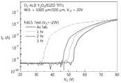
도 3 및 도 4는 어닐링 처리되지 않은 산화물 박막 트랜지스터의 전기적 특성을 나타내는 그래프이고, 도 5 및 도 6은 본 발명의 일 실시예에 따라 어닐링 처리된 산화물 박막 트랜지스터의 전기적 특성을 나타내는 그래프이다.FIGS. 3 and 4 are graphs showing electrical characteristics of an oxide thin film transistor not annealed, and FIGS. 5 and 6 are graphs showing electrical characteristics of an oxide thin film transistor annealed according to an embodiment of the present invention.
구체적으로, 도3 및 도 4는 IGZO 활성층 상에 산소 전구체로서 오존(O3)을 이용한 원자층 증착법(ALD)(이하 'O3-ALD'라 함)을 통하여 Y2O3 패시베이션층을 증착한 박막 트랜지스터 소자의 게이트 전극 전압에 따른 S/D 전류량의 전기적 특성을 비교하여 나타내는 그래프이다. 도3 및 도 4에 있어서, 가로축은 게이트 전압(VG)을 나타내고, 세로축은 드레인 전류(ID)를 나타낸다.3 and 4, a Y2 O3 passivation layer is deposited on an IGZO active layer through an atomic layer deposition (ALD) method using ozone (O3 ) as an oxygen precursor (hereinafter referred to as 'O3 -ALD' And comparing the electrical characteristics of the S / D current amount according to the gate electrode voltage of one thin film transistor element. 3 and 4, the horizontal axis represents the gate voltage (VG ), and the vertical axis represents the drain current (ID ).
본 발명의 일 실시예에 따라 제조된 산화물 박막 트랜지스터는 ITO로 형성된 소스 및 드레인 전극, 플라즈마 인핸스드 원자층 증착법으로 증착한 IGZO 활성층, 연속 공정으로 플라즈마 인핸스드 원자층 증착법을 이용하고 산소 전구체로서 오존(O3)을 이용한 10 ㎚ 두께의 Y2O3 패시베이션층, 게이트 절연막 및 Al으로 형성된 게이트 전극을 포함한다.The oxide thin film transistor manufactured according to an embodiment of the present invention includes a source and a drain electrode formed of ITO, an IGZO active layer deposited by a plasma enhanced atomic layer deposition method, a plasma enhanced atomic layer deposition method using a continuous process, A 10-nm-thick Y2 O3 passivation layer using aluminum oxide (O3 ), a gate insulating film, and a gate electrode formed of Al.
도 3을 참조하면, 제1(1st), 제2(2nd) 및 제3(3rd)의 측정 값은 서로 상이하게 나타나, 그 전기적 특성이 변화하는 것을 확인할 수 있고, 이렇게 전기적 특성이 변화하는 소자는 실제 제품으로서 적용이 불가능하다.Referring to FIG. 3, the first, second, and third measured values are different from each other, and it can be confirmed that the electrical characteristics thereof change. Thus, Is not applicable as a practical product.
또한, 도 4를 참조하면, IGZO 활성층 상에 O3-ALD을 통하여 Y2O3 패시베이션층을 증착한 박막 트랜지스터 소자를 빛과 음의 전압 조건에서의 안정성 테스트(Negative bias light illumination stability test, NBLS)를 진행한 결과, O3-ALD Y2O3 패시베이션층은 빛을 전혀 막아주지 못하는 것을 확인할 수 있다. 여기서, 빛은 파장이 480 nm 이고, 이를 에너지로 환산했을 때 2.6 eV인 광원을 사용하였다.Further, FIG. 4, the stability test of the Y2 O3 passivation layer, a thin film transistor element a voltage condition of light and sound via deposition of the O3 -ALD on the IGZO active layer (Negative bias light illumination stability test, NBLS ). As a result, it can be confirmed that the O3 -ALD Y2 O3 passivation layer does not block the light at all. Here, the light has a wavelength of 480 nm and a light source of 2.6 eV in terms of energy is used.
한편, 도5 및 도 6은 IGZO 활성층 상에 O3-ALD을 통하여 Y2O3 패시베이션층을 증착한 박막 트랜지스터 소자를 어닐링 처리한 박막 트랜지스터 소자의 게이트 전극 전압에 따른 S/D 전류량의 전기적 특성을 비교하여 나타내는 그래프이다. 도5 및 도 6에 있어서, 가로축은 게이트 전압(VG)을 나타내고, 세로축은 드레인 전류(ID)를 나타낸다.On the other hand, 5 and 6 are electrical characteristics of the S / D the amount of current corresponding to the gate electrode voltage of the thin film transistor element which Y2 O3 passivation layer by annealing a thin film transistor element by depositing the O3 -ALD on the IGZO active layer As shown in FIG. 5 and 6, the horizontal axis represents the gate voltage (VG ), and the vertical axis represents the drain current (ID ).
본 발명의 일 실시예에 따라 제조된 산화물 박막 트랜지스터는 ITO로 형성된 소스 및 드레인 전극, 플라즈마 인핸스드 원자층 증착법으로 증착한 IGZO 활성층, 연속 공정으로 플라즈마 인핸스드 원자층 증착법을 이용하고 산소 전구체로서 오존(O3)을 이용한 10 ㎚ 두께의 Y2O3 패시베이션층, 게이트 절연막 및 Al으로 형성된 게이트 전극을 포함하고, 최종적으로 진공 상에서 200 ℃ 조건으로 10분간 어닐링 처리하였다.The oxide thin film transistor manufactured according to an embodiment of the present invention includes a source and a drain electrode formed of ITO, an IGZO active layer deposited by a plasma enhanced atomic layer deposition method, a plasma enhanced atomic layer deposition method using a continuous process, (Y3 O3 ) 10 nm thick Y2 O3 passivation layer, a gate insulating film, and a gate electrode formed of Al. Finally, the substrate was annealed at 200 ° C. for 10 minutes under a vacuum condition.
도 5를 참조하면, 제1(1st) 내지 제4(4th)의 측정 값 모두 거의 유사하게 나타나, 그 전기적 특성이 변화하지 않는 것을 확인할 수 있고, 이렇게 전기적 특성이 변화하지 않는 소자는 실제 제품으로서 적용이 가능하다.Referring to FIG. 5, it can be confirmed that the first (1st) to fourth (4th) measured values are almost similar, and that the electrical characteristics do not change. Thus, It is applicable.
또한, 도 6을 참조하면, IGZO 활성층 상에 O3-ALD을 통하여 Y2O3 패시베이션층을 증착한 박막 트랜지스터 소자를 어닐링 처리한 박막 트랜지스터 소자를 빛과 음의 전압 조건에서의 안정성 테스트를 진행한 결과, 어닐링 처리된 O3-ALD Y2O3 패시베이션층은 전기적 특성의 변화가 거의 없는 것으로 보아, 빛에 대하여 안정적인 것을 확인할 수 있다. 여기서, 빛은 도 4와 마찬가지로 파장이 480 nm 이고, 이를 에너지로 환산했을 때 2.6 eV인 광원을 사용하였다.In addition, the progress of the stability test in the Y2 O3 passivation layer, a thin film transistor of a thin film transistor element annealing treatment device with light and a negative voltage condition of the deposit through, O3 -ALD on the IGZO active layer Referring to Figure 6 As a result, it can be confirmed that the annealed O3 -ALD Y2 O3 passivation layer shows almost no change in electrical characteristics and is stable against light. Here, the light has a wavelength of 480 nm as in FIG. 4, and a light source of 2.6 eV in terms of energy is used.
이에 따라, 본 발명의 일 실시예에 따른 산화물 박막 트랜지스터는 산화물 반도체 박막 트랜지스터에 어닐링 처리를 수행함으로써 빛에 대한 안정성을 개선시킬 수 있음을 확인할 수 있다.Accordingly, it can be seen that the oxide thin film transistor according to an embodiment of the present invention can improve the stability to light by performing an annealing process on the oxide semiconductor thin film transistor.
이상과 같이 본 발명은 비록 한정된 실시예와 도면에 의해 설명되었으나, 본 발명은 상기의 실시예에 한정되는 것은 아니며, 본 발명이 속하는 분야에서 통상의 지식을 가진 자라면 이러한 기재로부터 다양한 수정 및 변형이 가능하다.While the invention has been shown and described with reference to certain preferred embodiments thereof, it will be understood by those of ordinary skill in the art that various changes in form and details may be made therein without departing from the spirit and scope of the invention as defined by the appended claims. This is possible.
그러므로, 본 발명의 범위는 설명된 실시예에 국한되어 정해져서는 아니 되며, 후술하는 특허청구범위뿐 아니라 이 특허청구범위와 균등한 것들에 의해 정해져야 한다.Therefore, the scope of the present invention should not be limited to the described embodiments, but should be determined by the equivalents of the claims, as well as the claims.
110: 기판120: 버퍼층
130a: 소스 전극130b: 드레인 전극
140: 활성층150: 보호층
160: 게이트 절연막층170: 게이트 전극
210: 기판220: 버퍼층
230: 게이트 전극240: 게이트 절연막층
250: 활성층260: 보호층
270a: 소스 전극270b: 드레인 전극110: substrate 120: buffer layer
130a:
140: active layer 150: protective layer
160: gate insulating film layer 170: gate electrode
210: substrate 220: buffer layer
230: gate electrode 240: gate insulating film layer
250: active layer 260: protective layer
270a: source electrode 270b: drain electrode
Claims (6)
Translated fromKorean상기 패시베이션층은 Y2O3로 이루어지고, 5 ㎚ 내지 100 ㎚ 범위의 두께를 가지며,
상기 패시베이션층은 산소 전구체로서 오존(O3)을 이용한 원자층 증착법(ALD)을 통하여 상기 활성층 상에 형성되고,
상기 산화물 박막 트랜지스터는 어닐링 처리되며,
상기 어닐링 처리는 진공 조건에서, 150℃ 내지 250℃ 범위의 온도로 10분 내지 1시간 동안 수행되는 것을 특징으로 하는 산화물 박막 트랜지스터.
1. An oxide thin film transistor comprising an active layer made of IGZO, which is made of an oxide semiconductor, and a passivation layer protecting the active layer,
Wherein the passivation layer is made of Y2 O3 and has a thickness in the range of 5 nm to 100 nm,
The passivation layer is formed on the active layer through atomic layer deposition (ALD) using ozone (O3 ) as an oxygen precursor,
The oxide thin film transistor is annealed,
Wherein the annealing treatment is performed under a vacuum condition at a temperature in the range of 150 ° C to 250 ° C for 10 minutes to 1 hour.
Priority Applications (1)
| Application Number | Priority Date | Filing Date | Title |
|---|---|---|---|
| KR1020160011195AKR101876011B1 (en) | 2016-01-29 | 2016-01-29 | Oxide thin film transistor and method of manufacturing the same |
Applications Claiming Priority (1)
| Application Number | Priority Date | Filing Date | Title |
|---|---|---|---|
| KR1020160011195AKR101876011B1 (en) | 2016-01-29 | 2016-01-29 | Oxide thin film transistor and method of manufacturing the same |
Publications (2)
| Publication Number | Publication Date |
|---|---|
| KR20170090622A KR20170090622A (en) | 2017-08-08 |
| KR101876011B1true KR101876011B1 (en) | 2018-07-06 |
Family
ID=59653188
Family Applications (1)
| Application Number | Title | Priority Date | Filing Date |
|---|---|---|---|
| KR1020160011195AExpired - Fee RelatedKR101876011B1 (en) | 2016-01-29 | 2016-01-29 | Oxide thin film transistor and method of manufacturing the same |
Country Status (1)
| Country | Link |
|---|---|
| KR (1) | KR101876011B1 (en) |
Families Citing this family (2)
| Publication number | Priority date | Publication date | Assignee | Title |
|---|---|---|---|---|
| KR102036971B1 (en)* | 2017-11-10 | 2019-11-26 | 연세대학교 산학협력단 | Oxide thin film transistor and method of manufacturing the same |
| KR102385114B1 (en)* | 2019-11-18 | 2022-04-12 | 고려대학교 산학협력단 | Multi-channel thin film transistor and manufacturing method by the same |
Citations (9)
| Publication number | Priority date | Publication date | Assignee | Title |
|---|---|---|---|---|
| KR100857455B1 (en)* | 2007-04-17 | 2008-09-08 | 한국전자통신연구원 | Method of manufacturing thin film transistor by patterning by forming protective film on oxide semiconductor film |
| KR20110066370A (en)* | 2009-12-11 | 2011-06-17 | 한국전자통신연구원 | Thin film transistor and its manufacturing method |
| JP5127183B2 (en)* | 2006-08-23 | 2013-01-23 | キヤノン株式会社 | Thin film transistor manufacturing method using amorphous oxide semiconductor film |
| KR20130019903A (en)* | 2011-08-18 | 2013-02-27 | 주성엔지니어링(주) | Thin film transistor and method of manufacturing the same |
| JP5189698B2 (en)* | 2008-08-27 | 2013-04-24 | 出光興産株式会社 | Field effect transistor, manufacturing method thereof, and sputtering target |
| KR20140018702A (en)* | 2012-08-03 | 2014-02-13 | 주성엔지니어링(주) | Thin film transistor and method of manufacturing the same |
| JP2014507794A (en)* | 2010-12-30 | 2014-03-27 | ジュスン エンジニアリング カンパニー リミテッド | Thin film transistor and manufacturing method thereof |
| US20140239291A1 (en)* | 2013-02-27 | 2014-08-28 | Inha-Industry Partnership Institute | Metal-oxide semiconductor thin film transistors and methods of manufacturing the same |
| JP2014197664A (en)* | 2012-11-30 | 2014-10-16 | 株式会社半導体エネルギー研究所 | Semiconductor device and manufacturing method of the same |
- 2016
- 2016-01-29KRKR1020160011195Apatent/KR101876011B1/ennot_activeExpired - Fee Related
Patent Citations (10)
| Publication number | Priority date | Publication date | Assignee | Title |
|---|---|---|---|---|
| JP5127183B2 (en)* | 2006-08-23 | 2013-01-23 | キヤノン株式会社 | Thin film transistor manufacturing method using amorphous oxide semiconductor film |
| KR100857455B1 (en)* | 2007-04-17 | 2008-09-08 | 한국전자통신연구원 | Method of manufacturing thin film transistor by patterning by forming protective film on oxide semiconductor film |
| JP5189698B2 (en)* | 2008-08-27 | 2013-04-24 | 出光興産株式会社 | Field effect transistor, manufacturing method thereof, and sputtering target |
| KR20110066370A (en)* | 2009-12-11 | 2011-06-17 | 한국전자통신연구원 | Thin film transistor and its manufacturing method |
| JP2014507794A (en)* | 2010-12-30 | 2014-03-27 | ジュスン エンジニアリング カンパニー リミテッド | Thin film transistor and manufacturing method thereof |
| KR20130019903A (en)* | 2011-08-18 | 2013-02-27 | 주성엔지니어링(주) | Thin film transistor and method of manufacturing the same |
| KR20140018702A (en)* | 2012-08-03 | 2014-02-13 | 주성엔지니어링(주) | Thin film transistor and method of manufacturing the same |
| JP2014197664A (en)* | 2012-11-30 | 2014-10-16 | 株式会社半導体エネルギー研究所 | Semiconductor device and manufacturing method of the same |
| US20140239291A1 (en)* | 2013-02-27 | 2014-08-28 | Inha-Industry Partnership Institute | Metal-oxide semiconductor thin film transistors and methods of manufacturing the same |
| KR20140106977A (en)* | 2013-02-27 | 2014-09-04 | 삼성전자주식회사 | Metal oxide semiconductor Thin Film Transistors having high performance and methods of manufacturing the same |
Also Published As
| Publication number | Publication date |
|---|---|
| KR20170090622A (en) | 2017-08-08 |
Similar Documents
| Publication | Publication Date | Title |
|---|---|---|
| KR100877153B1 (en) | A method of forming a nano semiconductor film for an electronic device and a thin film transistor including the semiconductor film | |
| US8101949B2 (en) | Treatment of gate dielectric for making high performance metal oxide and metal oxynitride thin film transistors | |
| JP5584960B2 (en) | Thin film transistor and display device | |
| TWI501403B (en) | A thin film transistor structure, and a thin film transistor and a display device having the same | |
| JP4616359B2 (en) | Method for forming ZnO semiconductor film for electronic device and thin film transistor including the semiconductor film | |
| JP5780902B2 (en) | Semiconductor thin film, thin film transistor and manufacturing method thereof | |
| KR100857455B1 (en) | Method of manufacturing thin film transistor by patterning by forming protective film on oxide semiconductor film | |
| CN102683422B (en) | Oxide thin film transistor and manufacture method, array base palte, display unit | |
| Cai et al. | High-performance transparent AZO TFTs fabricated on glass substrate | |
| TWI405335B (en) | Semiconductor structure and method of manufacturing same | |
| JP2007073559A (en) | Thin film transistor manufacturing method | |
| CN104241392A (en) | Thin-film transistor, preparation method of thin-film transistor, display substrate and display device | |
| CN103730373A (en) | Manufacturing method of semiconductor device and semiconductor device | |
| KR101876011B1 (en) | Oxide thin film transistor and method of manufacturing the same | |
| KR101417932B1 (en) | Thin film transistor having double layered semiconductor channel and method of manufacturing the thin film transistor | |
| KR100996644B1 (en) | Method of manufacturing ZnO TT | |
| KR20130113972A (en) | Method for manufacturing oxide thin film transistor | |
| JP2013062456A (en) | Thin-film device and method of manufacturing the same | |
| CN106992116B (en) | Method for manufacturing semiconductor device, array substrate and display device | |
| CN111370364A (en) | Array panel and method of making the same | |
| KR20140144068A (en) | Zinc target including fluroride, method of fabricationg zinc nitride thin film using the same and method of fabricating thin film transistor using the same | |
| JP2014082424A (en) | Semiconductor device manufacturing method | |
| TWI636507B (en) | Method of manufacturing thin film transistor | |
| KR20200057372A (en) | DOPED TIN OXIDE THIN FILE TRANSISTOR and manufacturing method thereof | |
| KR101303428B1 (en) | Oxide thin film transistor and thereof |
Legal Events
| Date | Code | Title | Description |
|---|---|---|---|
| A201 | Request for examination | ||
| PA0109 | Patent application | St.27 status event code:A-0-1-A10-A12-nap-PA0109 | |
| PA0201 | Request for examination | St.27 status event code:A-1-2-D10-D11-exm-PA0201 | |
| D13-X000 | Search requested | St.27 status event code:A-1-2-D10-D13-srh-X000 | |
| D14-X000 | Search report completed | St.27 status event code:A-1-2-D10-D14-srh-X000 | |
| E902 | Notification of reason for refusal | ||
| PE0902 | Notice of grounds for rejection | St.27 status event code:A-1-2-D10-D21-exm-PE0902 | |
| E13-X000 | Pre-grant limitation requested | St.27 status event code:A-2-3-E10-E13-lim-X000 | |
| P11-X000 | Amendment of application requested | St.27 status event code:A-2-2-P10-P11-nap-X000 | |
| P13-X000 | Application amended | St.27 status event code:A-2-2-P10-P13-nap-X000 | |
| PG1501 | Laying open of application | St.27 status event code:A-1-1-Q10-Q12-nap-PG1501 | |
| E902 | Notification of reason for refusal | ||
| PE0902 | Notice of grounds for rejection | St.27 status event code:A-1-2-D10-D21-exm-PE0902 | |
| E13-X000 | Pre-grant limitation requested | St.27 status event code:A-2-3-E10-E13-lim-X000 | |
| P11-X000 | Amendment of application requested | St.27 status event code:A-2-2-P10-P11-nap-X000 | |
| P13-X000 | Application amended | St.27 status event code:A-2-2-P10-P13-nap-X000 | |
| E701 | Decision to grant or registration of patent right | ||
| PE0701 | Decision of registration | St.27 status event code:A-1-2-D10-D22-exm-PE0701 | |
| GRNT | Written decision to grant | ||
| PR0701 | Registration of establishment | St.27 status event code:A-2-4-F10-F11-exm-PR0701 | |
| PR1002 | Payment of registration fee | St.27 status event code:A-2-2-U10-U11-oth-PR1002 Fee payment year number:1 | |
| PG1601 | Publication of registration | St.27 status event code:A-4-4-Q10-Q13-nap-PG1601 | |
| PC1903 | Unpaid annual fee | St.27 status event code:A-4-4-U10-U13-oth-PC1903 Not in force date:20210703 Payment event data comment text:Termination Category : DEFAULT_OF_REGISTRATION_FEE | |
| PC1903 | Unpaid annual fee | St.27 status event code:N-4-6-H10-H13-oth-PC1903 Ip right cessation event data comment text:Termination Category : DEFAULT_OF_REGISTRATION_FEE Not in force date:20210703 | |
| R18-X000 | Changes to party contact information recorded | St.27 status event code:A-5-5-R10-R18-oth-X000 | |
| PN2301 | Change of applicant | St.27 status event code:A-5-5-R10-R13-asn-PN2301 St.27 status event code:A-5-5-R10-R11-asn-PN2301 | |
| P22-X000 | Classification modified | St.27 status event code:A-4-4-P10-P22-nap-X000 |