KR101875794B1 - Display device and electronic device including display device - Google Patents
Display device and electronic device including display deviceDownload PDFInfo
- Publication number
- KR101875794B1 KR101875794B1KR1020177024408AKR20177024408AKR101875794B1KR 101875794 B1KR101875794 B1KR 101875794B1KR 1020177024408 AKR1020177024408 AKR 1020177024408AKR 20177024408 AKR20177024408 AKR 20177024408AKR 101875794 B1KR101875794 B1KR 101875794B1
- Authority
- KR
- South Korea
- Prior art keywords
- layer
- oxide semiconductor
- gate
- semiconductor layer
- transistor
- Prior art date
- Legal status (The legal status is an assumption and is not a legal conclusion. Google has not performed a legal analysis and makes no representation as to the accuracy of the status listed.)
- Active
Links
Images


Classifications
- H—ELECTRICITY
- H10—SEMICONDUCTOR DEVICES; ELECTRIC SOLID-STATE DEVICES NOT OTHERWISE PROVIDED FOR
- H10D—INORGANIC ELECTRIC SEMICONDUCTOR DEVICES
- H10D86/00—Integrated devices formed in or on insulating or conducting substrates, e.g. formed in silicon-on-insulator [SOI] substrates or on stainless steel or glass substrates
- H10D86/40—Integrated devices formed in or on insulating or conducting substrates, e.g. formed in silicon-on-insulator [SOI] substrates or on stainless steel or glass substrates characterised by multiple TFTs
- H10D86/60—Integrated devices formed in or on insulating or conducting substrates, e.g. formed in silicon-on-insulator [SOI] substrates or on stainless steel or glass substrates characterised by multiple TFTs wherein the TFTs are in active matrices
- G—PHYSICS
- G09—EDUCATION; CRYPTOGRAPHY; DISPLAY; ADVERTISING; SEALS
- G09G—ARRANGEMENTS OR CIRCUITS FOR CONTROL OF INDICATING DEVICES USING STATIC MEANS TO PRESENT VARIABLE INFORMATION
- G09G3/00—Control arrangements or circuits, of interest only in connection with visual indicators other than cathode-ray tubes
- G09G3/20—Control arrangements or circuits, of interest only in connection with visual indicators other than cathode-ray tubes for presentation of an assembly of a number of characters, e.g. a page, by composing the assembly by combination of individual elements arranged in a matrix no fixed position being assigned to or needed to be assigned to the individual characters or partial characters
- G09G3/22—Control arrangements or circuits, of interest only in connection with visual indicators other than cathode-ray tubes for presentation of an assembly of a number of characters, e.g. a page, by composing the assembly by combination of individual elements arranged in a matrix no fixed position being assigned to or needed to be assigned to the individual characters or partial characters using controlled light sources
- G09G3/30—Control arrangements or circuits, of interest only in connection with visual indicators other than cathode-ray tubes for presentation of an assembly of a number of characters, e.g. a page, by composing the assembly by combination of individual elements arranged in a matrix no fixed position being assigned to or needed to be assigned to the individual characters or partial characters using controlled light sources using electroluminescent panels
- G09G3/32—Control arrangements or circuits, of interest only in connection with visual indicators other than cathode-ray tubes for presentation of an assembly of a number of characters, e.g. a page, by composing the assembly by combination of individual elements arranged in a matrix no fixed position being assigned to or needed to be assigned to the individual characters or partial characters using controlled light sources using electroluminescent panels semiconductive, e.g. using light-emitting diodes [LED]
- G09G3/3208—Control arrangements or circuits, of interest only in connection with visual indicators other than cathode-ray tubes for presentation of an assembly of a number of characters, e.g. a page, by composing the assembly by combination of individual elements arranged in a matrix no fixed position being assigned to or needed to be assigned to the individual characters or partial characters using controlled light sources using electroluminescent panels semiconductive, e.g. using light-emitting diodes [LED] organic, e.g. using organic light-emitting diodes [OLED]
- H01L27/1225—
- G—PHYSICS
- G09—EDUCATION; CRYPTOGRAPHY; DISPLAY; ADVERTISING; SEALS
- G09G—ARRANGEMENTS OR CIRCUITS FOR CONTROL OF INDICATING DEVICES USING STATIC MEANS TO PRESENT VARIABLE INFORMATION
- G09G3/00—Control arrangements or circuits, of interest only in connection with visual indicators other than cathode-ray tubes
- G09G3/20—Control arrangements or circuits, of interest only in connection with visual indicators other than cathode-ray tubes for presentation of an assembly of a number of characters, e.g. a page, by composing the assembly by combination of individual elements arranged in a matrix no fixed position being assigned to or needed to be assigned to the individual characters or partial characters
- G09G3/2003—Display of colours
- G—PHYSICS
- G09—EDUCATION; CRYPTOGRAPHY; DISPLAY; ADVERTISING; SEALS
- G09G—ARRANGEMENTS OR CIRCUITS FOR CONTROL OF INDICATING DEVICES USING STATIC MEANS TO PRESENT VARIABLE INFORMATION
- G09G3/00—Control arrangements or circuits, of interest only in connection with visual indicators other than cathode-ray tubes
- G09G3/20—Control arrangements or circuits, of interest only in connection with visual indicators other than cathode-ray tubes for presentation of an assembly of a number of characters, e.g. a page, by composing the assembly by combination of individual elements arranged in a matrix no fixed position being assigned to or needed to be assigned to the individual characters or partial characters
- G09G3/22—Control arrangements or circuits, of interest only in connection with visual indicators other than cathode-ray tubes for presentation of an assembly of a number of characters, e.g. a page, by composing the assembly by combination of individual elements arranged in a matrix no fixed position being assigned to or needed to be assigned to the individual characters or partial characters using controlled light sources
- G09G3/30—Control arrangements or circuits, of interest only in connection with visual indicators other than cathode-ray tubes for presentation of an assembly of a number of characters, e.g. a page, by composing the assembly by combination of individual elements arranged in a matrix no fixed position being assigned to or needed to be assigned to the individual characters or partial characters using controlled light sources using electroluminescent panels
- G09G3/32—Control arrangements or circuits, of interest only in connection with visual indicators other than cathode-ray tubes for presentation of an assembly of a number of characters, e.g. a page, by composing the assembly by combination of individual elements arranged in a matrix no fixed position being assigned to or needed to be assigned to the individual characters or partial characters using controlled light sources using electroluminescent panels semiconductive, e.g. using light-emitting diodes [LED]
- G09G3/3208—Control arrangements or circuits, of interest only in connection with visual indicators other than cathode-ray tubes for presentation of an assembly of a number of characters, e.g. a page, by composing the assembly by combination of individual elements arranged in a matrix no fixed position being assigned to or needed to be assigned to the individual characters or partial characters using controlled light sources using electroluminescent panels semiconductive, e.g. using light-emitting diodes [LED] organic, e.g. using organic light-emitting diodes [OLED]
- G09G3/3225—Control arrangements or circuits, of interest only in connection with visual indicators other than cathode-ray tubes for presentation of an assembly of a number of characters, e.g. a page, by composing the assembly by combination of individual elements arranged in a matrix no fixed position being assigned to or needed to be assigned to the individual characters or partial characters using controlled light sources using electroluminescent panels semiconductive, e.g. using light-emitting diodes [LED] organic, e.g. using organic light-emitting diodes [OLED] using an active matrix
- G09G3/3233—Control arrangements or circuits, of interest only in connection with visual indicators other than cathode-ray tubes for presentation of an assembly of a number of characters, e.g. a page, by composing the assembly by combination of individual elements arranged in a matrix no fixed position being assigned to or needed to be assigned to the individual characters or partial characters using controlled light sources using electroluminescent panels semiconductive, e.g. using light-emitting diodes [LED] organic, e.g. using organic light-emitting diodes [OLED] using an active matrix with pixel circuitry controlling the current through the light-emitting element
- H01L27/3244—
- H—ELECTRICITY
- H10—SEMICONDUCTOR DEVICES; ELECTRIC SOLID-STATE DEVICES NOT OTHERWISE PROVIDED FOR
- H10D—INORGANIC ELECTRIC SEMICONDUCTOR DEVICES
- H10D30/00—Field-effect transistors [FET]
- H10D30/60—Insulated-gate field-effect transistors [IGFET]
- H10D30/67—Thin-film transistors [TFT]
- H10D30/6704—Thin-film transistors [TFT] having supplementary regions or layers in the thin films or in the insulated bulk substrates for controlling properties of the device
- H10D30/6706—Thin-film transistors [TFT] having supplementary regions or layers in the thin films or in the insulated bulk substrates for controlling properties of the device for preventing leakage current
- H—ELECTRICITY
- H10—SEMICONDUCTOR DEVICES; ELECTRIC SOLID-STATE DEVICES NOT OTHERWISE PROVIDED FOR
- H10D—INORGANIC ELECTRIC SEMICONDUCTOR DEVICES
- H10D30/00—Field-effect transistors [FET]
- H10D30/60—Insulated-gate field-effect transistors [IGFET]
- H10D30/67—Thin-film transistors [TFT]
- H10D30/674—Thin-film transistors [TFT] characterised by the active materials
- H10D30/6755—Oxide semiconductors, e.g. zinc oxide, copper aluminium oxide or cadmium stannate
- H10D30/6756—Amorphous oxide semiconductors
- H—ELECTRICITY
- H10—SEMICONDUCTOR DEVICES; ELECTRIC SOLID-STATE DEVICES NOT OTHERWISE PROVIDED FOR
- H10D—INORGANIC ELECTRIC SEMICONDUCTOR DEVICES
- H10D30/00—Field-effect transistors [FET]
- H10D30/60—Insulated-gate field-effect transistors [IGFET]
- H10D30/67—Thin-film transistors [TFT]
- H10D30/6757—Thin-film transistors [TFT] characterised by the structure of the channel, e.g. transverse or longitudinal shape or doping profile
- H—ELECTRICITY
- H10—SEMICONDUCTOR DEVICES; ELECTRIC SOLID-STATE DEVICES NOT OTHERWISE PROVIDED FOR
- H10D—INORGANIC ELECTRIC SEMICONDUCTOR DEVICES
- H10D86/00—Integrated devices formed in or on insulating or conducting substrates, e.g. formed in silicon-on-insulator [SOI] substrates or on stainless steel or glass substrates
- H10D86/40—Integrated devices formed in or on insulating or conducting substrates, e.g. formed in silicon-on-insulator [SOI] substrates or on stainless steel or glass substrates characterised by multiple TFTs
- H10D86/421—Integrated devices formed in or on insulating or conducting substrates, e.g. formed in silicon-on-insulator [SOI] substrates or on stainless steel or glass substrates characterised by multiple TFTs having a particular composition, shape or crystalline structure of the active layer
- H10D86/423—Integrated devices formed in or on insulating or conducting substrates, e.g. formed in silicon-on-insulator [SOI] substrates or on stainless steel or glass substrates characterised by multiple TFTs having a particular composition, shape or crystalline structure of the active layer comprising semiconductor materials not belonging to the Group IV, e.g. InGaZnO
- H—ELECTRICITY
- H10—SEMICONDUCTOR DEVICES; ELECTRIC SOLID-STATE DEVICES NOT OTHERWISE PROVIDED FOR
- H10K—ORGANIC ELECTRIC SOLID-STATE DEVICES
- H10K59/00—Integrated devices, or assemblies of multiple devices, comprising at least one organic light-emitting element covered by group H10K50/00
- H10K59/10—OLED displays
- H10K59/12—Active-matrix OLED [AMOLED] displays
- H10K59/121—Active-matrix OLED [AMOLED] displays characterised by the geometry or disposition of pixel elements
- H10K59/1213—Active-matrix OLED [AMOLED] displays characterised by the geometry or disposition of pixel elements the pixel elements being TFTs
- H—ELECTRICITY
- H10—SEMICONDUCTOR DEVICES; ELECTRIC SOLID-STATE DEVICES NOT OTHERWISE PROVIDED FOR
- H10K—ORGANIC ELECTRIC SOLID-STATE DEVICES
- H10K59/00—Integrated devices, or assemblies of multiple devices, comprising at least one organic light-emitting element covered by group H10K50/00
- H10K59/10—OLED displays
- H10K59/12—Active-matrix OLED [AMOLED] displays
- H10K59/131—Interconnections, e.g. wiring lines or terminals
- G—PHYSICS
- G09—EDUCATION; CRYPTOGRAPHY; DISPLAY; ADVERTISING; SEALS
- G09G—ARRANGEMENTS OR CIRCUITS FOR CONTROL OF INDICATING DEVICES USING STATIC MEANS TO PRESENT VARIABLE INFORMATION
- G09G2330/00—Aspects of power supply; Aspects of display protection and defect management
- G09G2330/02—Details of power systems and of start or stop of display operation
- G09G2330/021—Power management, e.g. power saving
Landscapes
- Engineering & Computer Science (AREA)
- Physics & Mathematics (AREA)
- Computer Hardware Design (AREA)
- General Physics & Mathematics (AREA)
- Theoretical Computer Science (AREA)
- Microelectronics & Electronic Packaging (AREA)
- Geometry (AREA)
- Thin Film Transistor (AREA)
- Electroluminescent Light Sources (AREA)
- Devices For Indicating Variable Information By Combining Individual Elements (AREA)
- Control Of Indicators Other Than Cathode Ray Tubes (AREA)
- Control Of El Displays (AREA)
- Liquid Crystal (AREA)
- Shift Register Type Memory (AREA)
- Liquid Crystal Display Device Control (AREA)
Abstract
Translated fromKoreanDescription
Translated fromKorean본 발명의 일 형태는 표시 장치 및 표시 장치를 갖는 전자 기기에 관한 것이다. 특히, 산화물 반도체를 이용한 전계 효과형 트랜지스터와 발광소자에 의해 구성되는 표시 장치 및 표시 장치를 갖는 전자 기기에 관한 것이다.One aspect of the present invention relates to a display apparatus and an electronic apparatus having the display apparatus. In particular, the present invention relates to a field effect transistor using an oxide semiconductor, and a display device composed of the light emitting device and an electronic device having the display device.
절연 표면을 갖는 기판 상에 형성된 반도체 박막을 이용하여 박막 트랜지스터(TFT)를 구성하는 기술이 주목을 받고 있다. 박막 트랜지스터는 액정 TV로 대표될 수 있는 표시 장치에 사용되고 있다. 박막 트랜지스터에 적용 가능한 반도체 박막으로서 실리콘계 반도체 재료가 잘 알려져 있으나, 그 밖의 재료로서 산화물 반도체가 주목을 받고 있다.A technique of forming a thin film transistor (TFT) using a semiconductor thin film formed on a substrate having an insulating surface has attracted attention. The thin film transistor is used in a display device which can be represented by a liquid crystal TV. Silicon-based semiconductor materials are well known as semiconductor thin films applicable to thin film transistors, but oxide semiconductors are attracting attention as other materials.
산화물 반도체의 재료로서는 산화 아연 또는 산화 아연을 성분으로 하는 것이 알려져 있다. 그리고, 전자 캐리어 농도가 1018/cm3 미만인 비정질 산화물(산화물 반도체)로 형성된 박막 트랜지스터가 개시되어 있다(특허문헌 1 내지 3).As the material of the oxide semiconductor, it is known that zinc oxide or zinc oxide is used as a component. In addition, a thin film transistor formed of an amorphous oxide (oxide semiconductor) having an electron carrier concentration of less than 1018 / cm3 is disclosed (
산화물 반도체를 사용한 전계 효과형 트랜지스터는 예를 들어 표시 장치에 적용할 수 있다. 표시 장치로는, 광을 발생시켜 화상을 표시하는 자발광형의 표시 장치와, 백라이트로부터의 광을 선택적으로 일부 투과시켜 화상을 표시하는 투과형의 표시 장치와, 외광을 반사시켜 화상을 표시하는 반사형의 표시 장치가 있다.A field effect transistor using an oxide semiconductor can be applied to a display device, for example. Examples of the display device include a self-luminous display device that generates light to display an image, a transmissive display device that selectively transmits a part of the light from the backlight to display an image, Type display device.
자발광형의 표시 장치 및 투과형의 표시 장치의 특징은 외광의 영향을 쉽게 받지 않아 선명한 색을 나타내어 영상의 표현 능력이 뛰어나다.The characteristics of the self-luminous display device and the transmissive display device are not easily affected by the external light, so that they exhibit a clear color and excellent image expressing ability.
반사형의 표시 장치의 특징은 광원을 내장할 필요가 없으므로 소비 전력의 절감이 용이한 점에 있다. 물론 표시 화상을 다시 기입할 수 있어 인쇄 매체를 대체하는 전자 페이퍼로서 자원 절약을 지향하는 사회에서 주목을 받고 있다.A characteristic of the reflection type display device is that there is no need to incorporate a light source, so that the power consumption can be easily reduced. Of course, the display image can be rewritten and has attracted attention in a society that aims to save resources as an electronic paper replacing a print medium.
그러나, 외광이 적은 환경에서 반사형의 표시 장치는 시인성이 저하되므로 그 사용에는 조명이 필요하다. 조명을 사용하면 반사형의 표시 장치의 특징, 즉 소비 전력이 적은 특징이 훼손된다. 따라서, 특허문헌 4 및 특허문헌 5에는 소비 전력을 억제하면서 어두운 곳에서의 시인성을 높이기 위해 축광성 형광 재료나 축광 재료 등 외광을 축적하는 물질을 반사형의 표시 장치에 적용하는 발명이 개시되어 있다.However, in a reflective type display device in an environment with a small amount of external light, visibility deteriorates, and therefore, illumination is required for its use. If illumination is used, the characteristic of the reflection type display device, that is, the characteristic with low power consumption is damaged. Therefore, Patent Document 4 and
산화물 반도체는 박막 형성 공정에 있어서 화학양론적 조성에 의해 불균일이 발생한다. 예를 들어, 산소의 과부족에 의해 산화물 반도체의 전기 전도도가 변화된다. 또한, 산화물 반도체의 박막 형성 동안에 혼입되는 수소가 산소(O)-수소(H) 결합을 형성하여 전자 공여체가 되어 전기 전도도를 변화시키는 요인이 된다. 나아가 O-H는 극성 분자이므로 산화물 반도체에 의해 제조되는 박막 트랜지스터와 같은 능동 디바이스에 대해 특성의 변동 요인이 된다.The oxide semiconductors are uneven due to the stoichiometric composition in the thin film forming process. For example, the electrical conductivity of the oxide semiconductor is changed by excess or shortage of oxygen. In addition, the hydrogen introduced during the thin film formation of the oxide semiconductor forms an oxygen (O) -hydrogen (H) bond and becomes an electron donor, thereby changing the electric conductivity. Further, since O-H is a polar molecule, the characteristic of the active device such as a thin film transistor manufactured by an oxide semiconductor becomes a factor of variation.
전자 캐리어 농도가 1018/cm3 미만이어도 산화물 반도체에서는 실질적으로는 n형이며, 상기 특허문헌에 개시되는 박막 트랜지스터의 온/오프비는 103 밖에 되지 않는다. 이러한 박막 트랜지스터의 온/오프비가 낮은 이유는 오프 전류가 높음에 따른 것이다.Even though the electron carrier concentration is less than 1018 / cm3, the oxide semiconductor is substantially n-type, and the on / off ratio of the thin film transistor disclosed in the patent document is only 103 . The on / off ratio of the thin film transistor is low because of the high off current.
오프 전류가 높은 박막 트랜지스터를 표시 장치의 화소부에 사용했을 경우, 화소에 인가한 신호 전압을 유지하기 위해 용량을 추가로 마련할 필요가 발생한다. 화소에 용량을 마련하면 화소의 개구율이 저하되고 표시 장치의 소비 전력이 증가하는 과제가 있다.When a thin film transistor having a high off current is used for the pixel portion of the display device, it is necessary to additionally provide a capacitance for holding the signal voltage applied to the pixel. There is a problem that the aperture ratio of the pixel is lowered and the power consumption of the display device is increased by providing a capacitor for the pixel.
또한, 자발광형이나 투과형의 표시 장치의 소비 전력을 감소시키기 위해 상기 표시 장치가 갖는 발광소자로 공급하는 에너지를 감소시키면 표시가 어두워지거나 또는 사라지는 등 표시 품위에 미치는 영향이 현저하다.Further, if the energy supplied to the light emitting element included in the display device is reduced in order to reduce the power consumption of the self-luminous type or the transmissive type display device, the influence on the display quality such as darkening or disappearance of the display is remarkable.
또한, 상기 특허문헌에 개시되는 축광 재료를 적용한 반사형의 표시 장치는 외광이 적은 환경에서도 낮은 소비 전력으로 표시가 가능하나, 미리 외광을 축광 재료에 조사하여 축광 재료에 광을 축적해 둘 필요가 있고 어두운 곳에서의 장시간 사용에는 적합하지 않다.Further, the reflection type display device to which the phosphorescent material described in the patent document is applied can display with low power consumption even in an environment with little external light, but it is necessary to previously store external light in the phosphorescent material to accumulate light in the phosphorescent material It is not suitable for long time use in dark places.
본 발명은, 이러한 기술적 배경 하에서 이루어진 것이다. 따라서 그 목적은, 소비 전력이 억제된 표시 장치를 제공하는 것을 일 과제로 한다. 또한, 소비 전력이 억제된 자발광형의 표시 장치를 제공하는 것을 일 과제로 한다. 또한, 어두운 곳에서도 장시간의 이용이 가능한, 소비 전력이 억제된 자발광형의 표시 장치를 제공하는 것을 일 과제로 한다.The present invention has been made under such technical background. Therefore, an object of the present invention is to provide a display device in which power consumption is suppressed. It is another object of the present invention to provide a self-emission type display device in which power consumption is suppressed. It is another object of the present invention to provide a self-luminous display device in which power consumption is suppressed, which can be used even in a dark place for a long time.
본 발명의 일 형태는, 안정된 전기적 특성(예를 들어, 오프 전류가 극히 감소됨)을 갖는 박막 트랜지스터를 적용한 자발광형의 표시 장치이다. 구체적으로는, 산화물 반도체 내에서 전자 공여체(도너)가 되는 불순물을 제거함으로써 진성 또는 실질적으로 진성인 반도체로, 실리콘 반도체보다 에너지갭이 큰 산화물 반도체로 채널 영역이 형성되는 박막 트랜지스터에 의해 발광소자의 구동회로를 구성하는 것이다.One aspect of the present invention is a self-emission type display device to which a thin film transistor having stable electrical characteristics (for example, an extremely low off current) is applied. Specifically, by removing the impurity which becomes an electron donor (donor) in the oxide semiconductor, a channel region is formed of an intrinsic or substantially intrinsic semiconductor and an oxide semiconductor having an energy gap larger than that of the silicon semiconductor, And constitutes a driving circuit.
즉, 본 발명의 일 형태는, 산화물 반도체에 포함되는 수소가 5×10¹⁹/cm3 이하 바람직하게는 5×10¹⁸/cm3 이하, 보다 바람직하게는 5×10¹⁷/cm3 이하로 하여 산화물 반도체에 포함되는 수소 또는 OH결합을 제거하고 캐리어 농도를 1×10¹⁴/cm3 미만, 바람직하게는 1×10¹²/cm3 이하로 한 산화물 반도체막으로 채널 영역이 형성되는 박막 트랜지스터에 의해 발광소자의 구동회로를 구성하는 것이다.That is, one aspect of the present invention, the hydrogen contained in the
에너지갭은 2eV 이상, 바람직하게는 2.5eV 이상, 보다 바람직하게는 3eV 이상으로 하여 도너를 형성하는 수소 등의 불순물을 최대한 감소시키고 캐리어 농도를 1×10¹⁴/cm3 미만, 바람직하게는 1×10¹²/cm3 이하가 되도록 한다.Energy gap is 2eV or more, preferably at least 2.5eV, more preferably less than reduced the most of the impurities such as hydrogen to form a donor 3eV or more and 1 × 10¹⁴ / cm3 of the carrier concentration, preferably 1 × 10 <12 > / cm <3 > or less.
이와 같이 고순도화된 산화물 반도체는 박막 트랜지스터의 채널 형성 영역에 이용함으로써 채널폭이 10mm인 경우일지라도 드레인 전압이 1V 및 10V인 경우에 게이트 전압이 -5V에서 -20V인 범위에 있어서 드레인 전류는 1×10-13A 이하가 되도록 작용한다.The high purity oxide semiconductor is used in the channel forming region of the thin film transistor, so that even when the channel width is 10 mm, in the case where the drain voltage is 1 V and 10 V, the drain current is in the range of -5 V to -20 V, 10-13 A or less.
또한, 본 발명의 일 태양은 자발광형의 표시 장치가 갖는 구동회로가 소비하는 전력에 착안했다. 즉, 상기 구동회로가 동작하는 빈도를 줄여 그 표시 장치가 소비하는 전력을 억제할 수 있다. 또한, 자발광형 표시 장치의 화소부에 축광층을 마련하여 축광층에 발광소자가 발생하는 광을 축적하고, 축광층이 발생하는 광이 화상을 표시하고 있는 동안에 발광소자로 공급하는 에너지를 억제하여 표시 장치의 소비 전력을 억제할 수 있다.In addition, one aspect of the present invention has focused on the power consumed by the drive circuit of the self-luminous display device. That is, the frequency with which the driving circuit is operated can be reduced, and the power consumed by the display device can be suppressed. Further, a phosphorescent layer is provided in the pixel portion of the self-luminous display device to accumulate the light generated by the light emitting element in the phosphorescent layer, thereby suppressing the energy supplied to the light emitting element while the light generated by the phosphorescent layer displays the image So that the power consumption of the display device can be suppressed.
즉, 본 발명의 일 태양은, 화소에 펄스상의 직류 전력을 공급하는 전원선과, 전원선으로부터 전력이 공급되는 발광소자와, 전원선과 발광소자를 접속하는 회로의 개폐를 제어하는 제1 박막 트랜지스터를 갖는다. 또한, 영상 신호를 공급하는 신호선과, 신호선과 제1 박막 트랜지스터를 접속하는 회로의 개폐를 제어하는 제2 박막 트랜지스터를 갖는다. 상기 제2 박막 트랜지스터의 채널 형성 영역은 밴드 갭이 2eV 이상이며, 수소 농도가 5×10¹⁹/cm3 이하인 산화물 반도체로 형성되어 있다. 채널폭 1㎛ 당 오프 전류가 1×10-16A/m 이하로 억제된 제2 박막 트랜지스터가 제1 박막 트랜지스터의 온 상태를 유지하고, 상기 전원선과 상기 발광소자를 접속하여 정지 화상을 표시하는 표시 장치이다.According to an aspect of the present invention, there is provided a liquid crystal display device comprising: a power source line for supplying a pulse-like DC power to a pixel; a light emitting element for supplying power from a power source line; and a first thin film transistor for controlling opening and closing of a circuit connecting the power source line and the light emitting element . Further, the liquid crystal display device has a signal line for supplying a video signal and a second thin film transistor for controlling opening and closing of a circuit connecting the signal line and the first thin film transistor. The channel forming region of the second thin film transistor is formed of an oxide semiconductor having a band gap of 2 eV or more and a hydrogen concentration of 5 x 10¹⁹ / cm3 or less. The second thin film transistor in which the off current is suppressed to 1 x 10 <-16 > A / m or less per 1 m channel width maintains the ON state of the first thin film transistor and connects the power source line and the light emitting element to display a still image Display device.
또한, 본 발명의 일 태양은, 산화물 반도체층의 캐리어 농도가 1×10¹⁴/cm3 미만인 상기한 표시 장치이다.Further, one aspect of the present invention is the above-described display device wherein the carrier concentration of the oxide semiconductor layer is less than 1 x 10 <14 > / cm <3 >.
또한, 본 발명의 일 태양은, 정지 화상의 표시 기간 동안에 주사선 신호의 출력이 정지되는 기간을 갖는 상기한 표시 장치이다.Further, one aspect of the present invention is the above-described display device having a period during which the output of the scanning line signal is stopped during the display period of the still image.
또한, 본 발명의 일 태양은, 발광소자가 한 쌍의 전극과, 한 쌍의 전극간에 발광성의 유기물질을 포함하는 층을 갖는 상기한 표시 장치이다.Further, one aspect of the present invention is a display device as described above, wherein the light emitting element has a pair of electrodes and a layer containing a luminescent organic material between the pair of electrodes.
또한, 본 발명의 일 태양은, 화소에 축광층을 갖는 상기한 표시 장치이다.Further, one aspect of the present invention is the above-described display device having a phosphorescent layer in a pixel.
또한, 본 발명의 일 태양은, 상기 표시 장치를 구비하는 전자 기기이다.Further, one aspect of the present invention is an electronic apparatus having the display device.
아울러 본 명세서에서, 축광 재료는 외광 등의 외부로부터의 에너지를 흡수하여 비교적 안정적이며 수명이 긴 여기자를 생성하는 재료로서, 이 여기자가 비교적 긴 기간에 걸쳐 발광한 후 활성을 잃는 재료 전반을 가리킨다. 수명이 긴 여기자가 축적된 축광 재료는 외부로부터의 에너지가 끊긴 후에도 발광을 계속한다.In this specification, a phosphorescent material is a material which absorbs energy from the outside such as external light to generate a relatively stable excimer with a long lifetime, and refers to a material which loses activity after the exciton emits light for a relatively long period of time. The phosphorescent material in which excitons with long lifetimes are accumulated continues to emit light even after the energy from the outside is cut off.
아울러 본 명세서에서, 화소는 표시 장치의 각 화소에 마련된 각 소자, 예를 들어 박막 트랜지스터, 화소 전극으로서 기능하는 전극, 및 배선 등의 전기적인 신호에 의해 표시를 제어하기 위한 소자로 구성되는 소자군을 의미한다. 또한 화소는 컬러필터 등을 포함하는 것일 수도 있고, 1화소에 의해 밝기를 제어할 수 있는 하나의 색 요소에 해당할 수도 있다. 따라서, 일례로서 RGB의 색 요소로 이루어지는 컬러 표시 장치의 경우에는, 화상의 최소 단위는 R의 화소와 G의 화소와 B의 화소의 3화소로 구성되며, 복수의 화소에 의해 화상을 얻을 수 있다.In the present specification, a pixel is a device group composed of elements provided in each pixel of a display device, for example, a thin film transistor, an electrode functioning as a pixel electrode, and an element for controlling display by an electrical signal such as wiring . Further, the pixel may include a color filter or the like, or may correspond to one color element capable of controlling the brightness by one pixel. Thus, for example, in the case of a color display device composed of R, G, and B color elements, the minimum unit of the image is composed of R pixels, G pixels and B pixels, and an image can be obtained by a plurality of pixels .
아울러 본 명세서에서 A와 B가 접속되어 있다고 기재하는 경우는, A와 B가 전기적으로 접속되어 있는 경우와 A와 B가 직접 접속되어 있는 경우를 포함하는 것으로 한다. 여기서, A, B는 대상물(예를 들어, 장치, 소자, 회로, 배선, 전극, 단자, 도전막, 층 등)인 것으로 한다.In this specification, when A and B are connected, it is assumed that A and B are electrically connected and A and B are directly connected. Here, A and B are assumed to be objects (e.g., devices, elements, circuits, wires, electrodes, terminals, conductive films, layers, etc.).
아울러 본 명세서에서 EL층은 발광소자의 한 쌍의 전극 사이에 마련된 층을 가리키는 것으로 한다. 따라서, 전극 사이에 마련된 발광 물질인 유기 화합물을 포함하는 발광층은 EL층의 일 태양이다.In this specification, the EL layer refers to a layer provided between a pair of electrodes of the light emitting element. Therefore, the light emitting layer including the organic compound which is the light emitting substance provided between the electrodes is an aspect of the EL layer.
또한, 본 명세서에서, 물질 A를 다른 물질 B로 이루어지는 매트릭스 내에 분산시키는 경우, 매트릭스를 구성하는 물질 B를 호스트 재료라 부르고 매트릭스 내에 분산되는 물질 A를 게스트 재료라 부르기로 한다. 아울러 물질 A 및 물질 B는 각각 단일의 물질일 수도 있고, 2 종류 이상의 물질의 혼합물일 수도 있다.Further, in the present specification, when the substance A is dispersed in a matrix composed of another substance B, the substance B constituting the matrix is referred to as a host material and the substance A dispersed in the matrix is referred to as a guest material. In addition, the substances A and B may be a single substance or a mixture of two or more substances, respectively.
아울러 본 명세서에서 발광 장치는 화상 표시 디바이스, 발광 디바이스 또는 광원(조명 장치 포함)을 의미한다. 또한, 발광 장치에 코넥터, 예를 들어 FPC(Flexible printed circuit) 또는 TAB(Tape Automated Bonding) 테이프 또는 TCP(Tape CarrierPackage)가 부착된 모듈, TAB 테이프나 TCP의 끝에 프린트 배선판이 마련된 모듈, 또는 발광소자가 형성된 기판에 COG(Chip On Glass) 방식에 의해 IC(집적회로)가 직접 실장된 모듈도 모두 발광 장치에 포함되는 것으로 한다.In the present specification, the light emitting device refers to an image display device, a light emitting device, or a light source (including a lighting device). In addition, a module in which a connector, for example, a flexible printed circuit (FPC), a tape automated bonding (TAB) tape or a tape carrier package (TCP) is attached to the light emitting device, a module in which a printed wiring board is provided at the end of a TAB tape or TCP, And a module in which an IC (integrated circuit) is directly mounted by a COG (Chip On Glass) method on the substrate on which the light emitting device is formed are all included in the light emitting device.
본 발명의 일 형태에 따르면, 고순도화된 산화물 반도체를 이용한 박막 트랜지스터로 회로를 구성함으로써, 표시 장치가 갖는 회로의 동작을 안정화시킬 수 있다. 또한, 오프 전류가 1×10-13A 이하로 감소되었으므로, 표시 장치의 화소로 인가한 신호 전압을 유지하는 용량을 추가로 마련할 필요가 없게 된다. 즉, 각 화소에 유지 용량을 마련하지 않아도 되므로 개구율을 향상시킬 수 있다. 개구율이 높아짐으로써 발광소자의 구동 전압이 억제되어 표시 장치의 소비 전력이 감소된다.According to one aspect of the present invention, the circuit operation of the display device can be stabilized by constituting the circuit with the thin film transistor using the oxide semiconductor of high purity. Further, since the off current is reduced to 1 x 10 <-13 > A or less, it is not necessary to additionally provide a capacity for holding the signal voltage applied to the pixel of the display device. That is, since it is not necessary to provide a holding capacitor in each pixel, the aperture ratio can be improved. By increasing the aperture ratio, the driving voltage of the light emitting element is suppressed, and the power consumption of the display device is reduced.
또한, 본 발명의 일 형태에 따른 박막 트랜지스터를 이용한 화소는 일정한 상태(영상 신호가 기입된 상태)를 유지하는 것이 가능해지므로 정지화를 표시하는 경우에도 안정된 동작을 할 수 있다. 또한, 구동회로의 동작 간격을 길게 할 수 있으므로 표시 장치의 소비 전력을 감소시킬 수 있다.In addition, since the pixel using the thin film transistor according to an embodiment of the present invention can maintain a constant state (a state in which a video signal is written), stable operation can be performed even when a still image is displayed. In addition, since the operation interval of the drive circuit can be increased, the power consumption of the display device can be reduced.
또한, 본 발명의 일 형태에 의하면, 외광이 약한 환경하에서도 사용 가능한 표시 장치를 제공할 수 있다. 또한, 소비 전력을 억제하여 화상을 표시할 수 있는 표시 장치를 제공할 수 있다.Further, according to one aspect of the present invention, a display device that can be used even in an environment in which external light is weak can be provided. Further, it is possible to provide a display device capable of suppressing power consumption and displaying an image.
도 1(A)는 실시형태에 따른 화소의 상면도이고 도 1(B)는 단면도이고,
도 2는 실시형태에 따른 표시 장치의 구성을 설명하는 도면이고,
도 3은 실시형태에 따른 화소에의 기입 기간과 유지 기간을 설명하는 도면이고,
도 4(A)는 실시형태에 따른 화소의 상면도이고 도 4(B)는 단면도이고,
도 5(A)는 실시형태에 따른 박막 트랜지스터의 상면도이고 도 5(B)는 단면도이고,
도 6(A) 내지 도 6(E)는 실시형태에 따른 박막 트랜지스터의 제조 공정을 설명하는 도면이고,
도 7(A)는 실시형태에 따른 박막 트랜지스터의 상면도이고 도 7B는 단면도이고,
도 8(A) 내지 도 8(E)는 실시형태에 따른 박막 트랜지스터의 제조 공정을 설명하는 도면이고,
도 9(A) 및 도 9(B)는 실시형태에 따른 박막 트랜지스터의 단면도이고,
도 10(A) 내지 도 10(E)는 실시형태에 따른 박막 트랜지스터의 제조 공정을 설명하는 도면이고,
도 11(A) 내지 도 11(E)는 실시형태에 따른 박막 트랜지스터의 제조 공정을 설명하는 도면이고,
도 12(A) 내지 도 12(D)는 실시형태에 따른 박막 트랜지스터의 제조 공정을 설명하는 도면이고,
도 13(A) 내지 도 13(D)는 실시형태에 따른 박막 트랜지스터의 제조 공정을 설명하는 도면이고,
도 14는 실시형태에 따른 박막 트랜지스터의 단면도이고,
도 15는 실시형태에 따른 화소의 등가 회로를 설명하는 도면이고,
도 16(A) 내지 도 16(C)는 실시형태에 따른 화소의 단면도이고,
도 17(A)는 실시형태에 따른 발광 장치의 상부면도이고 도 17(B)는 단면도이고,
도 18은 실시형태에 따른 화소의 단면도이고,
도 19(A) 내지 도 19(C)는 실시형태에 따른 전자 기기를 설명하는 도면이고,
도 20(A) 내지 도 20(C)는 실시형태에 따른 전자 기기를 설명하는 도면이고,
도 21은 산화물 반도체를 이용한 역스태거형의 박막 트랜지스터의 종단면도이고,
도 22(A) 및 도 22(B)는 도 21에 나타낸 A-A'단면에 있어서의 에너지밴드도(모식도)이고,
도 23(A)는 (A)게이트(G1)에 양의 전위(+VG)가 인가된 상태를 나타내고, 도 23B는 게이트(G1)에 음의 전위(-VG)가 인가된 상태를 나타낸 도면이고,
도 24는 진공 준위와 금속의 일함수(φM), 산화물 반도체의 전자 친화력(χ)의 관계를 나타낸 도면이고,
도 25는 실시형태에 따른 표시 장치의 구성을 설명하는 블록도이고,
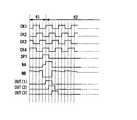
도 26(A) 내지 도 26(C)는 실시형태에 따른 구동회로 및 시프트 레지스터의 구성을 설명하는 도면이고,
도 27은 시프트 레지스터의 동작을 설명하는 타이밍차트이고,
도 28은 시프트 레지스터의 동작을 설명하는 타이밍차트이다.Fig. 1A is a top view of a pixel according to an embodiment, Fig. 1B is a sectional view,
2 is a view for explaining a configuration of a display device according to the embodiment,
Fig. 3 is a view for explaining a writing period and a sustaining period in the pixel according to the embodiment,
FIG. 4A is a top view of a pixel according to the embodiment, FIG. 4B is a sectional view,
FIG. 5A is a top view of a thin film transistor according to the embodiment, FIG. 5B is a sectional view,
6 (A) to 6 (E) are views for explaining a manufacturing process of a thin film transistor according to the embodiment,
FIG. 7A is a top view of a thin film transistor according to the embodiment, FIG. 7B is a sectional view,
8 (A) to 8 (E) are views for explaining a manufacturing process of the thin film transistor according to the embodiment,
9 (A) and 9 (B) are cross-sectional views of a thin film transistor according to an embodiment,
10 (A) to 10 (E) are diagrams for explaining a manufacturing process of the thin film transistor according to the embodiment,
11 (A) to 11 (E) are diagrams for explaining a manufacturing process of the thin film transistor according to the embodiment,
12 (A) to 12 (D) are diagrams for explaining a manufacturing process of the thin film transistor according to the embodiment,
13 (A) to 13 (D) are diagrams for explaining a manufacturing process of the thin film transistor according to the embodiment,
14 is a cross-sectional view of the thin film transistor according to the embodiment,
15 is a view for explaining an equivalent circuit of a pixel according to the embodiment,
Figs. 16A to 16C are cross-sectional views of pixels according to the embodiment,
FIG. 17A is a top view of a light emitting device according to the embodiment, FIG. 17B is a sectional view,
18 is a cross-sectional view of a pixel according to the embodiment,
Figs. 19 (A) to 19 (C) are diagrams for explaining an electronic apparatus according to the embodiment,
20 (A) to 20 (C) are diagrams for explaining an electronic apparatus according to the embodiment,
21 is a longitudinal sectional view of a reverse stagger type thin film transistor using an oxide semiconductor,
Figs. 22A and 22B are energy band diagrams (schematic diagrams) at the AA 'cross section shown in Fig. 21,
23A shows a state in which a positive potential (+ VG) is applied to the gate G1, FIG. 23B shows a state in which a negative potential (-VG) is applied to the gate G1 ,
24 is a graph showing the relationship between the vacuum level and the work function? M of the metal and the electron affinity (?) Of the oxide semiconductor,
25 is a block diagram for explaining the configuration of a display device according to the embodiment,
26A to 26C are diagrams for explaining the configurations of the driving circuit and the shift register according to the embodiment,
27 is a timing chart for explaining the operation of the shift register,
28 is a timing chart for explaining the operation of the shift register.
실시형태에 대해 도면을 이용하여 상세히 설명한다. 단, 본 발명은 이하의 설명에 한정되지 않고 본 발명의 취지 및 그 범위를 벗어나지 않고 그 형태 및 상세를 다양하게 변경할 수 있음을 당업자라면 용이하게 이해할 수 있을 것이다. 따라서, 본 발명은 이하에 나타내는 실시형태의 기재 내용에 한정하여 해석되는 것은 아니다. 아울러 이하에 설명하는 발명의 구성에 있어서 동일 부분 또는 동일한 기능을 갖는 부분에는 동일한 부호를 다른 도면들에서 공통적으로 사용하고 그 반복 설명은 생략한다.Embodiments will be described in detail with reference to the drawings. It is to be understood, however, that the present invention is not limited to the following description, and that various changes and modifications may be made without departing from the spirit and scope of the present invention. Therefore, the present invention is not construed as being limited to the description of the embodiments described below. In the following description of the present invention, the same reference numerals are used for the same parts or portions having the same functions, and the repetitive description thereof will be omitted.
(실시형태 1)(Embodiment 1)
본 실시형태에서는, 고순도화된 산화물 반도체를 이용한 박막 트랜지스터와 화소 전극으로 구성하는 화소의 예를, 도 1(A) 내지 도 1(C), 도 2, 도 3 및 도 4(A) 및 도 4(B)를 이용하여 이하에 설명한다.In this embodiment, examples of pixels constituted of a thin film transistor and a pixel electrode using a high-purity oxide semiconductor are shown in Figs. 1A to 1C, Figs. 2, 3 and 4A and Figs. 4 (B).
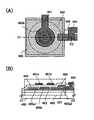
우선, 화소의 상면도를 도 1(A)에 나타내었다. 또한 도 1(A)에 도시된 TFT의 구조는, 일례로서 보텀 게이트형 구조에 대해 도시하였으며 게이트가 되는 배선에서 보아 채널 영역이 되는 산화물 반도체층 반대측에, TFT의 소스 전극 및 드레인 전극이 되는 배선층을 갖는, 이른바 역스태거형의 구성에 대해 도시하고 있다. 도 1(A)에 나타낸 화소(100)는 주사선으로서 기능하는 제1 배선(101), 신호선으로서 기능하는 제2 배선(102A), 산화물 반도체층(103), 용량선(104), 화소 전극(105)을 갖는다. 또한, 산화물 반도체층(103)과 화소 전극(105)을 전기적으로 접속하기 위한 제3 배선(102B)을 가지며, 이로써 박막 트랜지스터(106)가 구성된다.First, a top view of a pixel is shown in Fig. The structure of the TFT shown in Fig. 1 (A) is shown as an example of the bottom gate structure as an example. On the opposite side of the oxide semiconductor layer which becomes the channel region as viewed from the gate wiring, Called stagger-type configuration, which has a structure shown in Fig. A
제1 배선(101)은 박막 트랜지스터(106)의 게이트로서 기능하는 배선이기도 하다. 제2 배선(102A)은 소스 전극 또는 드레인 전극 중 하나 및 유지 용량의 하나의 전극으로서 기능하는 배선이기도 하다. 제3 배선(102B)은 소스 전극 또는 드레인 전극 중 다른 하나로서 기능하는 배선이기도 하다. 용량선(104)은 유지 용량의 다른 하나의 전극으로서 기능하는 배선이다. 또한 제1 배선(101)과 용량선(104)이 같은 층에 마련되고 제2 배선(102A)과 제3 배선(102B)이 같은 층에 마련된다. 또 제3 배선(102B)과 용량선(104)은 일부 중첩하여 마련되어 발광소자의 유지 용량을 형성하고 있다. 아울러 박막 트랜지스터(106)가 갖는 산화물 반도체층(103)은, 제1 배선(101)에서 분기된 배선 상에 게이트 절연막(도시하지 않음)을 사이에 두고 마련되어 있다.The
또한 도 1(B)에는 도 1(A)의 일점쇄선 A1-A2 간의 단면 구조에 대해 나타내고 있다. 도 1(B)에 도시된 단면 구조에서, 기판(111) 상에는, 하지막(112)을 사이에 두고, 게이트인 제1 배선(101), 용량선(104)이 마련되어 있다. 제1 배선(101) 및 용량선(104)을 덮도록 게이트 절연막(113)이 마련되어 있다. 게이트 절연막(113) 상에는 산화물 반도체층(103)이 마련되어 있다. 산화물 반도체층(103) 상에는 제2 배선(102A), 제3 배선(102B)이 마련되어 있다. 또한, 산화물 반도체층(103), 제2 배선(102A), 및 제3 배선(102B) 상에는, 패시베이션막으로서 기능하는 산화물 절연층(114)이 마련되어 있다. 산화물 절연층(114)에는 개구부가 형성되어 있고 개구부에서 화소 전극(105)과 제3 배선(102B)과의 접속이 이루어진다. 또한, 제3 배선(102B) 및 용량선(104)은 게이트 절연막(113)을 유전체로 하여 용량 소자를 형성하고 있다.Fig. 1 (B) shows the cross-sectional structure between the one-dot chain line A1-A2 in Fig. 1 (A). In the sectional structure shown in Fig. 1 (B), on the
또한 도 1(C)에는, 도 1(A)의 일점쇄선 B1-B2의 단면도에 대해 도시되어 있으며, 용량선(104)과 제2 배선(102A)과의 사이에 절연층(121)을 갖는 구성에 대해 나타내고 있다.1C is a sectional view taken along one-dot chain line B1-B2 in Fig. 1 (A), in which an insulating
제1 배선(101) 및 용량선(104) 상에 제2 배선(102A)을 마련하는 경우, 게이트 절연막(113)의 두께에 따라서는, 제1 배선(101)과 제2 배선(102A), 및 용량선(104)과 제2 배선(102A) 사이에 기생 용량이 발생하게 된다. 따라서 도 1(C)에 도시된 바와 같이 절연층(121)을 마련함으로써 기생 용량을 줄여 오동작 등의 불량을 감소시킬 수 있다.When the
아울러 도 1(A) 내지 (C)에 도시된 화소는, 도 2에 도시된 바와 같이 기판(200) 상에 복수의 화소(201)가 매트릭스형으로 배치되는 것이다. 도 2에서는, 기판(200) 상에는 화소부(202), 주사선 구동회로(203), 및 신호선 구동회로(204)를 갖는 구성에 대해 나타내고 있다. 화소(201)는 주사선 구동회로(203)에 접속된 제1 배선(101)에 의해 공급되는 주사 신호에 의해, 각 행마다 선택 상태 또는 비선택 상태가 결정된다. 또한 주사 신호에 의해 선택된 화소(201)는 신호선 구동회로(204)에 접속된 제2 배선(102A)에 의해 제2 배선(102A)으로부터 비디오 전압(영상 신호, 화상 신호, 비디오 신호, 비디오 데이터라고도 함)이 공급된다.1 (A) to (C), a plurality of
도 2에서는, 주사선 구동회로(203), 신호선 구동회로(204)가 기판(200) 상에 마련되는 구성에 대해 도시하였으나, 주사선 구동회로(203) 또는 신호선 구동회로(204) 중 어느 하나가 기판(200) 상에 마련되도록 구성으로 할 수도 있다. 또한 화소부(202)만을 기판(200) 상에 마련하도록 구성할 수도 있다.2 shows a structure in which the scanning
도 2에서 화소부(202)에는 복수의 화소(201)가 매트릭스형으로 배치(스트라이프 배치)되는 예에 대해 나타내고 있다. 아울러 화소(201)는 반드시 매트릭스형으로 배치될 필요는 없고, 예를 들어, 화소(201)를 델타 배치, 또는 베이어 배치할 수도 있다. 또한 화소부(202)의 표시 방식은 프로그래시브 방식, 인터레이스 방식 중 어느 하나를 이용할 수 있다. 아울러 컬러 표시할 때에 화소에서 제어하는 색 요소로서는 RGB(R는 빨강, G는 초록, B는 파랑)의 3색으로 한정되지 않고 그 이상일 수도 있고, 예를 들어 RGBW(W는 흰색), 또는 RGB에, 옐로우, 시안, 마젠타 등을 하나 이상 추가한 것 등이 있다. 아울러 색 요소의 도트마다 그 표시 영역의 크기가 다를 수도 있다.In Fig. 2, the
도 2에서, 제1 배선(101) 및 제2 배선(102A)은 화소의 행방향 및 열방향의 수에 대응시켜 도시하고 있다. 또한 화소들 사이에 제1 배선(101) 및 제2 배선(102A)을 공유하여 화소(201)를 구동하도록 구성할 수도 있다.In Fig. 2, the
아울러 도 1(A)에서는 TFT의 제2 배선(102A)의 형상을 직사각형으로 도시하고 있으나, 제3 배선(102B)을 둘러싸는 형상(구체적으로는, U자형 또는 C자형)으로 하여 캐리어가 이동하는 영역의 면적을 증가시켜 박막 트랜지스터의 도통시에 흐르는 전류(온 전류라고도 함)의 양을 늘리도록 구성할 수도 있다.1 (A), the shape of the
또한 본 명세서에서 설명하는 온 전류는 박막 트랜지스터가 온 상태(도통 상태라고도 함)시에 소스와 드레인 사이에 흐르는 전류를 말한다. n채널형의 박막 트랜지스터에서는 게이트와 소스 사이에 인가되는 전압이 문턱 전압(Vth)보다 큰 경우에 소스와 드레인 사이를 흐르는 전류를 가리킨다.The ON current described in this specification refers to a current flowing between a source and a drain when the thin film transistor is in an ON state (also referred to as a conduction state). In an n-channel thin film transistor, a current flowing between a source and a drain when a voltage applied between a gate and a source is greater than a threshold voltage (Vth).
또한 개구율은 단위면적에 대해, 광이 통과하는 영역의 면적의 비율을 나타낸 것으로, 광을 투과시키지 않는 부재가 차지하는 영역이 넓어지면 개구율이 저하되고, 광을 투과시키는 부재가 차지하는 영역이 넓어지면 개구율이 향상된다. 표시 장치에서는, 화소 전극에 중첩되는 배선, 용량선이 차지하는 면적, 및 박막 트랜지스터의 사이즈를 작게 함으로써 개구율이 향상된다.The aperture ratio indicates the ratio of the area of the area through which light passes. When the area occupied by the member that does not transmit light is widened, the aperture ratio decreases. When the area occupied by the member that transmits light becomes wider, . In the display device, the aperture ratio is improved by reducing the size of the thin film transistor, the area occupied by the capacitor line, and the wiring superimposed on the pixel electrode.
특히 자발광형의 표시 장치에 있어서는, 관찰자가 표시 장치의 표시와 마주하는 위치에서 관찰할 수 있는 발광소자의 발광 면적이 화소 면적에서 차지하는 비율을 개구율이라고 한다.Particularly, in a self-luminous display device, the ratio of the light emitting area of the light emitting element to the pixel area that can be observed at the position where the observer faces the display of the display device is called the aperture ratio.
아울러 박막 트랜지스터는, 게이트와, 드레인과, 소스를 포함하는 적어도 3개의 단자를 갖는 소자이며, 드레인영역과 소스영역 사이에 채널 영역을 가지고 있으며, 드레인영역과 채널 영역과 소스영역을 통해 전류를 흐르게 할 수 있다. 여기서, 소스와 드레인은 서로, 트랜지스터의 구조나 동작 조건 등에 의해 바뀌므로 어느것이 소스 또는 드레인인지를 한정하기 어렵다. 따라서 소스 및 드레인으로서 기능하는 영역을 소스 또는 드레인이라고 부르지 않는 경우가 있다. 그 경우, 일례로서는 각각을 제1 단자, 제2 단자로 표기하는 경우가 있다. 또는, 각각을 제1 전극, 제2 전극으로 표기하는 경우가 있다. 또는, 제1 영역, 제2 영역이라고 표기하는 경우가 있다.The thin film transistor is a device having at least three terminals including a gate, a drain, and a source. The thin film transistor has a channel region between the drain region and the source region and flows a current through the drain region, the channel region, and the source region can do. Here, since the source and the drain are different from each other depending on the structure and operating conditions of the transistor, it is difficult to define which is the source or the drain. Therefore, a region functioning as a source and a drain may not be referred to as a source or a drain. In this case, as an example, the first terminal and the second terminal may be respectively referred to. Alternatively, each of the first electrode and the second electrode may be referred to as a first electrode or a second electrode. Alternatively, the first area and the second area may be referred to.
이어서 산화물 반도체층(103)에 대해 설명한다.Next, the
본 실시형태에서 사용하는 산화물 반도체는 수소 또는 OH결합이 제거되어 이 산화물 반도체에 포함되는 수소는 5×10¹⁹/cm3 이하, 바람직하게는 5×10¹⁸/cm3 이하, 보다 바람직하게는 5×10¹⁷/cm3 이하이다. 그리고, 캐리어 농도를 1×10¹⁴/cm3 미만, 바람직하게는 1×10¹²/cm3 이하로 한 산화물 반도체막을 채널 형성 영역에 적용하여 박막 트랜지스터를 구성한다. 아울러 산화물 반도체층 내의 수소 농도 측정은 2차 이온 질량 분석법(SIMS:Secondary Ion Mass Spectroscopy)으로 수행할 수 있다.In the oxide semiconductor used in the present embodiment, hydrogen or OH bonds are removed and the hydrogen contained in the oxide semiconductor is 5 x 10¹⁹ / cm3 or less, preferably 5 x 10¹⁸ / cm3 or less, more preferably 5 × 10¹⁷ / cm3 or less. Then, an oxide semiconductor film having a carrier concentration of less than 1 x 10¹⁴ / cm3 , preferably 1 x 10¹² / cm3 or less is applied to the channel forming region to constitute a thin film transistor. The hydrogen concentration in the oxide semiconductor layer can be measured by secondary ion mass spectroscopy (SIMS).
산화물 반도체의 에너지갭은 2eV 이상, 바람직하게는 2.5eV 이상, 보다 바람직하게는 3eV 이상으로 하여 도너를 형성하는 수소 등의 불순물을 최대한 감소시켜 캐리어 농도를 1×10¹⁴/cm3 미만, 바람직하게는 1×10¹²/cm3 이하가 되도록 한다. 즉, 산화물 반도체층의 캐리어 농도는 가능한 한 제로로 한다.The energy gap of the oxide semiconductor is more than 2eV, preferably at least 2.5eV, more preferably less than 1 × 10¹⁴ / cm3 of the carrier density by as much as possible reduce the impurities such as hydrogen to form a donor 3eV or more, preferably Lt;12 > / cm <3 > or less. That is, the carrier concentration of the oxide semiconductor layer is set to zero as much as possible.
이와 같이 산화물 반도체층에 포함되는 수소를 철저하게 제거함으로써 고순도화된 산화물 반도체층을 박막 트랜지스터의 채널 형성 영역에 이용하여 오프 전류값이 지극히 작은 박막 트랜지스터를 제공할 수 있다.By removing the hydrogen contained in the oxide semiconductor layer in this way, the oxide semiconductor layer of high purity can be used in the channel forming region of the thin film transistor, thereby providing a thin film transistor having an extremely small off current value.
예를 들어, 고순도화된 산화물 반도체층을 이용한 박막 트랜지스터의 채널 길이가 3㎛, 채널폭이 10mm인 경우일지라도 드레인 전압이 1V 및 10V인 경우에 게이트 전압이 -5V에서 -20V인 범위(오프 상태)에 있어서 드레인 전류는 1×10-13A 이하가 되도록 작용한다.For example, in the case where the channel length of the thin film transistor using the high-purity oxide semiconductor layer is 3 탆 and the channel width is 10 mm, the gate voltage is in the range of -5 V to -20 V (when the drain voltage is 1 V and 10 V ), The drain current functions to be 1 x 10 <-13 > A or less.
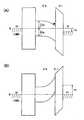
고순도화된 산화물 반도체층을 이용한 박막 트랜지스터의 특성에 대해 도 21 내지 도 24를 이용하여 설명한다. 도 21은, 산화물 반도체를 이용한 역스태거형의 박막 트랜지스터의 종단면도를 나타낸다. 게이트 전극(GE1) 상에 게이트 절연막(GI)을 사이에 두고 산화물 반도체층(OS)이 마련되고 그 위에 소스 전극(S) 및 드레인 전극(D)이 마련되어 있다.The characteristics of the thin film transistor using the highly purified oxide semiconductor layer will be described with reference to FIGS. 21 to 24. FIG. 21 is a longitudinal sectional view of a reverse stagger type thin film transistor using an oxide semiconductor. An oxide semiconductor layer OS is provided on the gate electrode GE1 with a gate insulating film GI sandwiched therebetween and a source electrode S and a drain electrode D are provided thereon.
도 22는, 도 21에 나타낸 A-A'단면에 있어서의 에너지밴드도(모식도)를 나타낸다. 도 22(A)는 소스와 드레인 사이의 전압을 등전위(VD=0V)로 했을 경우를 나타내고, 도 22(B)는 소스에 대해 드레인에 양의 전위(VD>0V)를 가했을 경우를 나타낸다.Fig. 22 shows an energy band diagram (schematic diagram) taken along the line A-A 'shown in Fig. 22A shows a case where the voltage between the source and the drain is set to an equal potential (VD = 0V), and FIG. 22B shows a case where a positive potential (VD> 0V) is applied to the drain with respect to the source.
도 23은 도 21의 B-B' 단면에 있어서의 에너지밴드도(모식도)이다. 도 23(A)은 게이트(G1)에 양의 전위(+VG)가 인가된 상태이며, 소스와 드레인 사이에 캐리어(전자)가 흐르는 온 상태를 나타내고 있다. 또한, 도 23(B)은 게이트(G1)에 음의 전위(-VG)가 인가된 상태이며, 오프 상태(소수 캐리어는 흐르지 않음)인 경우를 나타낸다.Fig. 23 is an energy band diagram (schematic diagram) taken along the line B-B 'in Fig. 23A shows a state in which a positive potential (+ VG) is applied to the gate G1 and an ON state in which carriers (electrons) flow between the source and the drain. 23 (B) shows a state in which a negative potential (-VG) is applied to the gate G1 and the off state (the minority carriers do not flow).
도 24는 진공 준위와 금속의 일함수(φM), 산화물 반도체의 전자 친화력(χ)의 관계를 나타낸다.24 shows the relationship between the vacuum level and the work function? M of the metal and the electron affinity (?) Of the oxide semiconductor.
종래의 산화물 반도체는 일반적으로 n형이며, 그 경우의 페르미 준위(Ef)는 밴드 갭 중앙에 위치하는 진성 페르미 준위(Ei)에서 떨어져 전도대 가까이에 위치하고 있다. 아울러 산화물 반도체에 있어서 수소의 일부는 도너가 되어 n형화되는 하나의 요인이 될 수 있음이 알려져 있다.The conventional oxide semiconductor is generally n-type, and the Fermi level (Ef) in this case is located near the conduction band away from the intrinsic Fermi level (Ei) located at the center of the band gap. It is also known that a part of hydrogen in the oxide semiconductor becomes a donor and becomes one of n-type.
이에 반해 본 발명에 따른 산화물 반도체는, n형 불순물인 수소를 산화물 반도체로부터 제거하여 산화물 반도체의 주성분 이외의 불순물이 최대한 포함되지 않도록 고순도화함으로써 진성(i형)으로 하거나 또는 진성형으로 하고자 한 것이다. 즉, 수소나 물 등의 불순물을 최대한 제거함으로써 고순도화된 i형(진성 반도체) 또는 이에 근접하도록 하는 것을 특징으로 하고 있다. 이에 따라 페르미 준위(Ef)는 진성 페르미 준위(Ei)와 동일한 레벨로 할 수도 있다.On the other hand, the oxide semiconductor according to the present invention is intended to be intrinsic (i-type) or intrinsic type by removing hydrogen from the n-type impurity from the oxide semiconductor and making the impurity other than the main component of the oxide semiconductor high- . That is, it is characterized in that impurities such as hydrogen and water are removed as much as possible to make i-type (intrinsic semiconductor) highly purified or coming close to it. Accordingly, the Fermi level Ef may be set to the same level as the intrinsic Fermi level Ei.
산화물 반도체의 밴드갭(Eg)이 3.15eV인 경우 전자 친화력(χ)은 4.3eV로 알려져 있다. 소스 전극 및 드레인 전극을 구성하는 티타늄(Ti)의 일함수는 산화물 반도체의 전자 친화력(χ)과 거의 같다. 이 경우, 금속-산화물 반도체 계면에 있어서 전자에 대해 쇼트키형의 장벽은 형성되지 않는다.When the band gap Eg of the oxide semiconductor is 3.15 eV, the electron affinity (x) is known to be 4.3 eV. The work function of titanium (Ti) constituting the source electrode and the drain electrode is almost equal to the electron affinity (x) of the oxide semiconductor. In this case, a Schottky barrier is not formed with respect to electrons in the metal-oxide semiconductor interface.
즉, 금속의 일함수(φM)와 산화물 반도체의 전자 친화력(χ)이 거의 같은 경우, 이 둘이 접촉하면 도 22(A)와 같은 에너지밴드도(모식도)가 나타난다.That is, when the work function? M of the metal and the electron affinity (?) Of the oxide semiconductor are substantially equal to each other, an energy band diagram (schematic diagram) as shown in FIG.
도 22(B)에서 검은 동그라미(●)는 전자를 나타내고, 드레인으로 양의 전위가 인가되면, 전자는 배리어(h)를 넘어 산화물 반도체로 주입되어 드레인을 향해 흐른다. 이 경우, 배리어(h)의 높이는 게이트 전압과 드레인 전압에 따라 변화되는데, 양의 드레인 전압이 인가되었을 경우에는, 전압 인가가 없는 도 22(A)의 배리어의 높이 즉 밴드갭(Eg)의 1/2보다 배리어의 높이(h)는 작은 값이 된다.In FIG. 22B, a black circle (●) represents electrons, and when a positive potential is applied to the drain, electrons are injected into the oxide semiconductor over the barrier h and flow toward the drain. In this case, the height of the barrier h varies depending on the gate voltage and the drain voltage. When the positive drain voltage is applied, the height of the barrier of Fig. 22A without voltage application, / 2, the height h of the barrier becomes smaller.
이 때 전자는 도 23(A)에서 나타낸 바와 같이 게이트 절연막과 고순도화된 산화물 반도체와의 계면에서의, 산화물 반도체측의 에너지적으로 안정된 최저부를 따라 이동한다.At this time, the electrons move along the lowest energy-stable part of the oxide semiconductor side at the interface between the gate insulating film and the highly-purified oxide semiconductor as shown in Fig. 23 (A).
또한, 도 23(B)에서 게이트 전극(G1)에 음의 전위가 인가되면 소수 캐리어인 홀은 실질적으로 제로가 되므로 전류는 최대한 제로에 가까운 값이 된다.23 (B), when a negative potential is applied to the gate electrode G1, the hole as a minority carrier becomes substantially zero, so that the current becomes as close to zero as possible.
예를 들어, 박막 트랜지스터의 채널폭(W)이 1×10⁴㎛이고 채널 길이가 3㎛인 소자에서도 오프 전류가 10-13A 이하이며 서브 스레쉬홀드 스윙값(S값)이 0.1V/dec.(게이트 절연 두께 100nm)를 얻을 수 있다.For example, even when the channel width W of the thin film transistor is 1 x 10⁴ 탆 and the channel length is 3 탆, the off current is 10-13 A or less and the subthreshold swing value (S value) is 0.1 V / dec. (
이와 같이 산화물 반도체의 주성분 이외의 불순물이 최대한 포함되지 않도록 고순도화함으로써 박막 트랜지스터의 동작을 양호하게 할 수 있다.In this manner, the operation of the thin film transistor can be improved by making the impurity other than the main component of the oxide semiconductor high-purity so as not to include as much as possible.
이와 같이, 오프 상태에서의 전류값(오프 전류값)이 극히 작은 박막 트랜지스터를 이용하여 기억회로(기억소자) 등을 제조했을 경우 오프 전류값이 작고 거의 리크가 없으므로 영상 신호 등의 전기신호를 유지하는 시간을 길게 할 수 있다.As described above, when a memory circuit (memory element) or the like is manufactured using a thin film transistor having an extremely small current value (off current value) in the OFF state, the off current value is small and almost no leakage occurs. Can be made longer.
구체적으로는 상술한 산화물 반도체층을 구비하는 박막 트랜지스터는 채널폭 1㎛ 당 오프 전류를 1×10-16A/m 이하로 하는 것, 나아가 1aA/m(1×10-18A/m) 이하로 하는 것이 가능하다.Specifically, the above-mentioned oxide thin film transistor having a semiconductor layer is to the off-current per
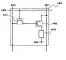
오프 상태에서의 전류값(오프 전류값)이 극히 작은 트랜지스터를 화소부의 스위칭용 트랜지스터(예를 들어 도 15의 스위칭용 트랜지스터(6401))로서 이용함으로써 영상 신호 등의 전기신호의 유지 시간을 길게 할 수 있다. 유지 시간을 길게 할 수 있으므로 예를 들어 기입의 간격은 10초 이상, 바람직하게는 30초 이상, 더욱 바람직하게는 1분 이상 10분 미만으로 할 수 있다. 기입하는 간격을 길게 하면 소비 전력을 억제하는 효과를 높일 수 있다.The transistor having the extremely small current value (off current value) in the OFF state is used as the switching transistor (for example, the switching
아울러 트랜지스터의 오프 전류가 흐르기 어려운 정도를 오프 저항율로서 나타낼 수 있다. 오프 저항율은 트랜지스터의 오프시의 채널 형성 영역의 저항율이며 오프 저항율은 오프 전류로부터 산출할 수 있다.It is also possible to express the degree of difficulty that the off current of the transistor hardly flows as the off resistivity. The off resistivity is the resistivity of the channel forming region when the transistor is off, and the off resistivity can be calculated from the off current.
구체적으로는, 오프 전류와 드레인 전압의 값을 알 수 있으면 오옴의 법칙으로부터 트랜지스터가 오프일 때의 저항값(오프 저항(R))을 산출할 수 있다. 그리고, 채널 형성 영역의 단면적(A)과 채널 형성 영역의 길이(소스 드레인 전극간의 거리에 상당)(L)를 알 수 있으면 ρ=RA/L의 식(R은 오프 저항)으로부터 오프 저항율(ρ)을 산출할 수 있다.Specifically, if the value of the off current and the drain voltage can be known, the resistance value (off-resistance R) when the transistor is off can be calculated from Ohm's law. If the cross-sectional area A of the channel forming region and the length L of the channel forming region (corresponding to the distance between the source and drain electrodes) can be known, the ratio of resistivity ρ ) Can be calculated.
여기서, 단면적(A)은 채널 형성 영역의 두께를 d로 하고 채널폭을 W로 할 때, A=dW로부터 산출할 수 있다. 또한, 채널 형성 영역의 길이(L)는 채널 길이(L)이다. 이상과 같이 오프 전류로부터 오프 저항율을 산출할 수 있다.Here, the cross-sectional area A can be calculated from A = dW where d is the thickness of the channel forming region and W is the channel width. In addition, the length L of the channel forming region is the channel length (L). As described above, the off resistivity can be calculated from the off current.
본 실시형태의 산화물 반도체층을 구비하는 트랜지스터의 오프 저항율은 1×10⁹Ω·m이상이 바람직하고, 나아가 1×10¹⁰Ω·m 이상이 보다 바람직하다.The off-resistivity of the transistor including the oxide semiconductor layer of the present embodiment is preferably 1 x 10 <9 > [Omega] m or more, more preferably 1 x10 <10 >
또한 도 15에 나타낸 화소 구성은 본 실시형태의 일 태양이며, 예를 들어 유지 용량을 구동용 트랜지스터(6402)의 게이트와 전원선(6407) 사이에 마련할 수도 있다. 이 유지 용량은, 한 쌍의 전극 사이에 절연층을 유전체로서 개재시켜 구성할 수 있다. 유지 용량의 크기는 스위칭용 트랜지스터(6401)의 오프 전류 등을 고려하여 소정 기간 동안 전하를 유지할 수 있도록 설정한다.The pixel structure shown in Fig. 15 is an aspect of this embodiment mode. For example, a holding capacitor may be provided between the gate of the driving
예를 들어 저온 폴리실리콘을 구비하는 박막 트랜지스터에서는, 오프 전류가 1×10-12A 상당하는 것으로 추측하여 설계 등을 수행하도록 되어 있다. 이 때문에 산화물 반도체를 갖는 박막 트랜지스터에서는 저온 폴리실리콘을 구비하는 박막 트랜지스터에 비해 유지 용량이 동등(0.1Pf 정도)할 때, 전압의 유지 기간을 105배 정도로 연장시킬 수 있다. 또한, 아몰퍼스(amorphous) 실리콘을 구비하는 트랜지스터의 경우, 채널폭 1㎛ 당 오프 전류는 1×10-13A/m 이상이다. 따라서, 유지 용량이 동등(0.1pF 정도)할 때 고순도의 산화물 반도체를 이용한 트랜지스터가 아몰퍼스(amorphous) 실리콘을 이용한 트랜지스터와 비교하여 전압의 유지 기간을 104배 이상으로 연장시킬 수 있다.For example, in a thin film transistor provided with low-temperature polysilicon, it is assumed that the off current corresponds to 1 x 10 <-12 > Therefore, in a thin film transistor having an oxide semiconductor, when the holding capacitance is equal (about 0.1 Pf) to the thin film transistor having a low temperature polysilicon, the voltage holding period can be extended to about 105 times. In the case of a transistor including amorphous silicon, the off current per 1 m channel width is 1 x 10 <-13 > A / m or more. Therefore, when the storage capacitance is equal (about 0.1 pF), the transistor using the high-purity oxide semiconductor can extend the voltage holding period to 104 times or more as compared with the transistor using amorphous silicon.
일례로서 통상 저온 폴리실리콘을 이용한 트랜지스터를 갖는 화소에서는 표시를 60프레임/초(1프레임 당 16msec)로 수행하고 있다. 이는 정지화의 경우에도 동일하며 레이트를 저하시키면(기입의 간격을 늘리면) 화소의 전압이 저하되어 표시에 지장을 초래하기 때문이다. 한편, 상술한 산화물 반도체층을 구비하는 트랜지스터를 이용했을 경우 오프 전류가 작으므로 한번의 신호 기입에 의한 유지 기간을 105배인 1600초 정도로 할 수 있다.As an example, in a pixel having a transistor using low-temperature polysilicon, display is performed at 60 frames / second (16 msec per frame). This is also true in the case of still image, and if the rate is lowered (the interval of writing is increased), the voltage of the pixel is lowered and the display is hindered. On the other hand, when the transistor including the above-described oxide semiconductor layer is used, since the off current is small, the sustain period by one signal writing can be made about 1600 seconds, which is 105 times.
이상과 같이 본 실시형태의 표시 장치는 적은 화상 신호의 기입 회수로 정지화의 표시를 수행할 수 있다. 유지 기간을 길게 취할 수 있으므로 특히 정지화의 표시를 수행할 때에 신호의 기입을 수행하는 빈도를 줄일 수 있다. 따라서 저소비전력화를 도모할 수 있다. 예를 들어, 하나의 정지 화상의 표시 기간에 화소에 기입하는 회수는 1회 또는 n회로 할 수 있다. 아울러 n은 2 이상 103회 이하로 한다. 이에 의해 표시 장치의 저소비전력화를 도모할 수 있다.As described above, the display apparatus according to the present embodiment can perform the display of the still image with the number of writing of a small number of image signals. It is possible to reduce the frequency of performing the writing of the signal when the display of the still image is performed. Therefore, the power consumption can be reduced. For example, the number of times of writing in the pixel in the display period of one still image may be one time or n times. Also, n should be 2 or more and 103 or less. As a result, the power consumption of the display device can be reduced.
나아가 본 실시형태에서는, 정지화 표시를 실시할 때에 신호선이나 주사선으로 공급되는 신호의 출력을 정지하도록 구동회로부를 동작시킴으로써 화소부 뿐만 아니라 구동회로부의 소비 전력도 억제할 수 있다.Further, in the present embodiment, when the still image display is performed, the driving circuit section is operated so as to stop the output of the signal supplied to the signal line or the scanning line, so that not only the pixel section but also the power consumption of the driving circuit section can be suppressed.
도 3에서는 기입 기간과 유지 기간(1 프레임 기간이라고도 함)의 관계에 대해 나타내고 있다. 도 3에서, 기간(251, 252)이 유지 기간에 상당하고, 기간(261, 262)이 기입 기간에 상당한다. 전술한 고순도화된 산화물 반도체층을 구비하는 박막 트랜지스터는 유지 기간(기간(251), 기간(252))을 길게 취할 수 있으므로 특히 정지화의 표시를 수행할 때에 신호의 기입을 수행하는 빈도를 현저하게 줄일 수 있다. 따라서 표시의 변환이 적은 정지화 등의 표시에서는, 화소로의 신호의 기입 회수를 줄일 수 있으므로 저소비전력화를 도모할 수 있다.In Fig. 3, the relationship between the writing period and the sustaining period (also referred to as one frame period) is shown. 3, the
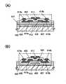
또한 EL소자에 접속된 구동 트랜지스터의 게이트로 인가된 전압은 정지화를 표시하고 있는 동안에 감쇠되므로 구동 트랜지스터의 게이트로 인가된 전압이 유지되고 있는 비율을 고려하여 적절히 리프레쉬 동작할 수도 있다. 예를 들어, 구동 트랜지스터의 게이트에 신호를 기입한 직후의 전압의 값(초기값)에 대해 소정의 레벨까지 전압이 내려간 타이밍에 리프레쉬 동작을 수행할 수 있다. 소정의 레벨의 전압은, 초기값에 대해서 깜박임을 느끼지 않는 정도로 설정하는 것이 바람직하다. 구체적으로는, 표시 대상이 영상인 경우, 초기값에 대해 1.0% 낮은 상태, 바람직하게는 0.3% 낮은 상태가 될 때마다 리프레쉬 동작(재기입)을 수행하는 것이 바람직하다. 또한, 표시 대상이 문자인 경우, 초기값에 대해서 10% 낮은 상태, 바람직하게는 3% 낮은 상태가 될 때마다 리프레쉬 동작(재기입)을 수행하는 것이 바람직하다.In addition, since the voltage applied to the gate of the driving transistor connected to the EL element is attenuated during the display of the still image, the refresh operation can be appropriately performed in consideration of the rate at which the voltage applied to the gate of the driving transistor is maintained. For example, the refresh operation can be performed at a timing when the voltage drops to a predetermined level with respect to the value (initial value) of the voltage immediately after the signal is written to the gate of the driving transistor. It is preferable that the voltage of the predetermined level is set to such a degree that it does not feel flickering with respect to the initial value. Specifically, when the display object is a video, it is preferable to perform the refresh operation (rewrite) every time the state becomes 1.0% lower, preferably 0.3% lower than the initial value. When the display object is a character, it is preferable to perform the refresh operation (rewrite) every time the state becomes 10% lower, preferably 3% lower than the initial value.
아울러 유지 용량을 형성하지 않는 경우의 화소의 상면도 및 그 단면도의 구성에 대해 도 4(A), (B)에 도시하였다. 도 4(A), (B)에 도시된 구성은, 도 1(A) 및 (B)에서의 용량선을 생략한 도면에 상당한다. 도 4(A)에 나타낸 상면도, 도 4(B)에 나타낸 단면도를 통해서도 알 수 있는 바와 같이, 산화물 반도체층을 갖는 박막 트랜지스터를 이용함으로써 화소 전극(105)이 차지하는 영역, 즉 개구율을 향상시킬 수 있다. 또한 도 4(B)에 나타낸 단면도를 통해서도 알 수 있는 바와 같이, 산화물 반도체층을 갖는 박막 트랜지스터를 이용함으로써 용량선을 삭감하고 그리고 화소 전극(105)이 차지하는 영역을 넓힐 수 있으므로 결국 개구율을 향상시킬 수 있다.FIGS. 4A and 4B show a top view and a cross-sectional view of the pixel in the case where the storage capacitor is not formed. FIG. The configurations shown in Figs. 4 (A) and 4 (B) correspond to drawings in which the capacitance lines in Figs. 1 (A) and 1 (B) are omitted. As can be seen from the top view shown in Fig. 4 (A) and the sectional view shown in Fig. 4 (B), the area occupied by the
본 실시형태와 같이 고순도화된 산화물 반도체층을 이용한, 오프 전류값이 극히 작은 박막 트랜지스터를 화소부에 적용함으로써 화소부에 유지 용량을 마련하지 않고서도 화상(특히 동영상)의 표시가 가능한 표시 장치를 제공할 수 있다. 또한 유지 용량을 마련하는 경우에 있어서도 유지 용량에서 전압을 유지할 수 있는 기간을 길게 취할 수 있어 정지화 등을 표시할 때의 소비 전력이 감소된 표시 장치를 제공할 수 있다. 아울러 개구율의 향상을 도모함으로써 고해상도의 표시부를 갖는 표시 장치를 제공할 수 있다.A thin film transistor using an oxide semiconductor layer of a high purity as in the present embodiment and having an extremely small off current value is applied to the pixel portion so that a display device capable of displaying an image (especially a moving picture) . Further, even in the case of providing the storage capacitor, the period in which the voltage can be held in the storage capacitor can be increased, and the display device in which the power consumption when displaying the static image or the like is reduced can be provided. Further, by improving the aperture ratio, it is possible to provide a display device having a display portion of high resolution.
본 실시형태는 다른 실시형태에 기재한 구성과 적절히 조합하여 실시하는 것이 가능하다.The present embodiment can be implemented in appropriate combination with the configuration described in the other embodiments.
(실시형태 2)(Embodiment 2)
본 실시형태는, 본 명세서에서 개시하는 표시 장치에 적용할 수 있는 박막 트랜지스터의 예를 나타낸다. 본 실시형태에서 나타내는 박막 트랜지스터(410)는 실시형태 1의 박막 트랜지스터(106)로서 이용할 수 있다.This embodiment shows an example of a thin film transistor applicable to the display device disclosed in this specification. The
본 실시형태의 박막 트랜지스터 및 박막 트랜지스터의 제조 방법의 일 형태를 도 5 및 도 6을 이용하여 설명한다.An embodiment of a method of manufacturing a thin film transistor and a thin film transistor of this embodiment will be described with reference to FIGS. 5 and 6. FIG.
도 5(A), (B)에 박막 트랜지스터의 표면 및 단면 구조의 일례를 나타낸다. 도 5(A), (B)에 나타낸 박막 트랜지스터(410)는 탑 게이트 구조의 박막 트랜지스터 중 하나이다.5A and 5B show an example of a surface and a sectional structure of the thin film transistor. The
도 5(A)는 탑 게이트 구조의 박막 트랜지스터(410)의 상면도이며, 도 5(B)는 도 5(A)의 선 C1-C2의 단면도이다.5A is a top view of a
박막 트랜지스터(410)는 절연 표면을 갖는 기판(400) 상에, 절연층(407), 산화물 반도체층(412), 소스 전극층 또는 드레인 전극층(415a), 및 소스 전극층 또는 드레인 전극층(415b), 게이트 절연층(402), 게이트 전극층(411)을 포함하고, 소스 전극층 또는 드레인 전극층(415a), 소스 전극층 또는 드레인 전극층(415b)에 각각 배선층(414a), 배선층(414b)이 접촉하여 마련되어 전기적으로 접속되어 있다.The
또한, 박막 트랜지스터(410)는 싱글 게이트 구조의 박막 트랜지스터를 이용하여 설명했으나, 필요에 따라서 채널 형성 영역을 복수 갖는 멀티 게이트 구조의 박막 트랜지스터도 형성할 수 있다.Though the
이하, 도 6(A) 내지 (E)를 이용하여 기판(400) 상에 박막 트랜지스터(410)를 제조하는 공정을 설명한다.Hereinafter, a process of manufacturing the
절연 표면을 갖는 기판(400)으로 사용할 수 있는 기판에 큰 제한은 없으나, 적어도 이후의 가열 처리에 견딜 수 있을 정도의 내열성을 가질 필요가 있다. 바륨보로실리케이트 유리나 알루미노보로실리케이트 유리 등의 유리 기판을 사용할 수 있다.There is no particular limitation on the substrate that can be used as the
또한, 유리 기판으로서는, 이후의 가열 처리의 온도가 높은 경우에는 변형점이 730℃ 이상인 것을 사용하는 것이 좋다. 또한, 유리 기판에는 예를 들어 알루미노실리케이트 유리, 알루미노보로실리케이트 유리, 바륨보로실리케이트 유리 등의 유리 재료가 사용되고 있다. 또한 산화 붕소에 비해 산화 바륨(BaO)을 많이 포함시킴으로써 보다 실용적인 내열유리를 얻을 수 있다. 따라서 B2O3보다 BaO를 많이 포함하는 유리 기판을 사용하는 것이 바람직하다.As the glass substrate, when the temperature of the subsequent heat treatment is high, it is preferable to use a glass substrate having a strain point of 730 캜 or higher. Glass substrates such as aluminosilicate glass, aluminoborosilicate glass, and barium borosilicate glass are used for the glass substrate. In addition, by containing a large amount of barium oxide (BaO) in comparison with boron oxide, a more practical heat-resistant glass can be obtained. Therefore, it is preferable to use a glass substrate containing more BaO than B2 O3 .
또한 상기한 유리 기판 대신에 세라믹 기판, 석영 기판, 사파이어 기판 등의 절연체인 기판을 사용할 수도 있다. 그 밖에도 결정화 유리 등을 사용할 수 있다. 또한, 플라스틱 기판 등도 적절히 사용할 수 있다.Instead of the above-described glass substrate, a ceramic substrate, a quartz substrate, a sapphire substrate, or other insulator substrate may be used. In addition, crystallized glass and the like can be used. A plastic substrate or the like can also be suitably used.
우선, 절연 표면을 갖는 기판(400) 상에 하지막이 되는 절연층(407)을 형성한다. 산화물 반도체층과 접하는 절연층(407)은, 산화 실리콘층, 산화 질화 실리콘층, 산화 알루미늄층, 또는 산화 질화 알루미늄층 등의 산화물 절연층을 사용하는 것이 바람직하다. 절연층(407)의 형성 방법으로서는 플라즈마 CVD법 또는 스퍼터링법 등을 이용할 수 있는데, 절연층(407) 내에 수소가 다량으로 포함되지 않도록 하기 위해서는 스퍼터링법으로 절연층(407)을 성막하는 것이 바람직하다.First, an insulating
본 실시형태에서는, 절연층(407)으로서 스퍼터링법에 의해 산화 실리콘층을 형성한다. 기판(400)을 처리실로 이송하고 수소 및 수분이 제거된 고순도 산소를 포함하는 스퍼터링 가스를 도입하고 실리콘 반도체의 타겟을 이용하여 기판(400)에 절연층(407)으로서 산화 실리콘층을 성막한다. 또한 기판(400)은 실온일 수도 있고 가열되어 있을 수도 있다.In this embodiment mode, a silicon oxide layer is formed as an insulating
예를 들어, 석영(바람직하게는 합성 석영)을 사용하고 기판 온도 108℃, 기판과 타겟 사이의 거리(T-S간 거리)를 60mm, 압력 0.4Pa, 고주파 전원 1.5kW, 산소 및 아르곤(산소 유량 25sccm:아르곤 유량 25sccm=1:1) 분위기하에서 RF 스퍼터링법에 의해 산화 실리콘막을 성막한다. 두께는 100nm로 한다. 또한 산화 실리콘막을 성막하기 위한 타겟으로서 석영(바람직하게는 합성 석영) 대신 실리콘 타겟을 사용할 수 있다. 또한 스퍼터링 가스로서 산소 또는, 산소 및 아르곤의 혼합 가스를 사용하여 수행한다.For example, using quartz (preferably synthetic quartz), the substrate temperature is 108 占 폚, the distance between the substrate and the target (distance between TS) is 60 mm, the pressure is 0.4 Pa, the high frequency power is 1.5 kW, oxygen and argon : A flow rate of argon gas of 25 sccm = 1: 1) to form a silicon oxide film by RF sputtering. The thickness is 100 nm. A silicon target may be used instead of quartz (preferably synthetic quartz) as a target for forming a silicon oxide film. And is performed using oxygen or a mixed gas of oxygen and argon as a sputtering gas.
이 경우에 처리실 내의 잔류 수분을 제거하면서 절연층(407)을 성막하는 것이 바람직하다. 절연층(407)에 수소, 수산기 또는 수분이 포함되지 않도록 하기 위함이다.In this case, it is preferable to form the insulating
처리실 내의 잔류 수분을 제거하기 위해서는 흡착형의 진공 펌프를 사용하는 것이 바람직하다. 예를 들어, 크라이오 펌프, 이온 펌프, 티타늄 서브리메이션 펌프를 사용하는 것이 바람직하다. 또한, 배기 수단은 터보 펌프에 콜드트랩을 부가한 것일 수도 있다. 크라이오 펌프를 이용하여 배기시킨 처리실은, 예를 들어, 수소 원자나, 물(H2O) 등 수소 원자를 포함하는 화합물을 포함하는 화합물 등이 배기되므로 이 처리실에서 성막한 절연층(407)에 포함되는 불순물의 농도를 감소시킬 수 있다.In order to remove the residual moisture in the treatment chamber, it is preferable to use an adsorption type vacuum pump. For example, it is preferable to use a cryo pump, an ion pump, and a titanium sublimation pump. Further, the exhaust means may be one in which a cold trap is added to the turbo pump. The treatment chamber exhausted by using the cryopump is exhausted from the treatment chamber, for example, a hydrogen atom or a compound containing a compound containing a hydrogen atom such as water (H2 O) It is possible to reduce the concentration of the impurities contained in the impurities.
절연층(407)을 성막할 때에 이용하는 스퍼터링 가스는 수소, 물, 수산기 또는 수소화물 등의 불순물이, 농도 ppm 정도, 바람직하게는 농도 ppb 정도까지 제거된 고순도 가스를 사용하는 것이 바람직하다.The sputtering gas used when forming the insulating
스퍼터링법에는 스퍼터링용 전원으로 고주파 전원을 이용하는 RF 스퍼터링법과 직류 전원을 이용하는 DC 스퍼터링법, 나아가 펄스적으로 바이어스를 주는 펄스 DC 스퍼터링법이 있다. RF 스퍼터링법은 주로 절연막을 성막하는 경우에 이용되고 DC 스퍼터링법은 주로 금속막을 성막하는 경우에 이용된다.As the sputtering method, there are an RF sputtering method using a high frequency power source as a power source for sputtering, a DC sputtering method using a DC power source, and a pulse DC sputtering method giving a pulse bias. The RF sputtering method is mainly used for forming an insulating film, and the DC sputtering method is mainly used for forming a metal film.
또한, 재료가 다른 타겟을 복수 설치할 수 있는 다원 스퍼터링 장치도 있다. 다원 스퍼터링 장치는 동일 챔버에서 다른 재료막을 적층 성막할 수도, 동일 챔버에서 복수 종류의 재료를 동시에 방전시켜 성막할 수도 있다.There is also a multi-sputtering apparatus in which a plurality of targets having different materials can be provided. The multi-sputtering apparatus may be formed by depositing another material film in the same chamber or by simultaneously discharging a plurality of kinds of materials in the same chamber.
또한, 챔버 내부에 자석 기구를 구비한 마그네트론 스퍼터링법을 이용하는 스퍼터링 장치나, 글로우 방전을 이용하지 않고 마이크로파를 이용하여 발생시킨 플라즈마를 이용하는 ECR 스퍼터링법을 이용하는 스퍼터링 장치가 있다.There is also a sputtering apparatus using a magnetron sputtering method having a magnet mechanism in a chamber and a sputtering apparatus using an ECR sputtering method using plasma generated by using microwaves without using a glow discharge.
또한, 스퍼터링법을 이용하는 성막 방법으로서 성막시에 타겟 물질과 스퍼터링 가스 성분을 화학반응시켜 그 화합물 박막을 형성하는 리엑티브 스퍼터링법이나, 성막시에 기판에도 전압을 인가하는 바이어스 스퍼터링법도 있다.As a film forming method using the sputtering method, there is also a reactive sputtering method in which a target material and a sputtering gas component are chemically reacted with each other during film formation to form a thin film of the compound, or a bias sputtering method in which a voltage is applied to a substrate at the time of film formation.
또한, 절연층(407)은 적층 구조일 수도 있고, 예를 들어, 기판(400) 상에 질화 실리콘층, 질화 산화 실리콘층, 질화 알루미늄층 또는 질화 산화 알루미늄층 등의 질화물 절연층과 상기 산화물 절연층을 적층한 구조로 할 수도 있다.The insulating
예를 들어, 산화 실리콘층과 기판 사이에 수소 및 수분이 제거된 고순도 질소를 포함하는 스퍼터링 가스를 도입하고 실리콘 타겟을 이용하여 질화 실리콘층을 성막한다. 이 경우에도 산화 실리콘층과 마찬가지로, 처리실 내의 잔류 수분을 제거하면서 질화 실리콘층을 성막하는 것이 바람직하다.For example, a sputtering gas containing hydrogen and moisture-removed high-purity nitrogen is introduced between the silicon oxide layer and the substrate, and a silicon nitride layer is formed using the silicon target. Also in this case, it is preferable to form the silicon nitride layer while removing the residual moisture in the treatment chamber, similarly to the silicon oxide layer.
질화 실리콘층을 형성하는 경우에도 성막시에 기판을 가열할 수도 있다.The substrate may be heated at the time of film formation even when the silicon nitride layer is formed.
절연층(407)으로서 질화 실리콘층과 산화 실리콘층을 적층하는 경우, 질화 실리콘층과 산화 실리콘층을 같은 처리실에서 공통의 실리콘 타겟을 이용하여 성막할 수 있다. 먼저 질소를 포함하는 가스를 도입하고, 처리실 내에 장착된 실리콘 타겟을 이용하여 질화 실리콘층을 형성하고 이어서 산소를 포함하는 가스로 바꾸어 동일한 실리콘 타겟을 이용하여 산화 실리콘층을 성막한다. 질화 실리콘층과 산화 실리콘층을 대기에 노출시키지 않고 연속적으로 형성할 수 있으므로 질화 실리콘층 표면에 수소나 수분 등의 불순물이 흡착하는 것을 방지할 수 있다.When the silicon nitride layer and the silicon oxide layer are stacked as the insulating
이어서 절연층(407) 상에 두께 2nm 이상 200nm 이하의 산화물 반도체막을 형성한다.Then, an oxide semiconductor film having a thickness of 2 nm or more and 200 nm or less is formed on the insulating
또한, 산화물 반도체막에 수소, 수산기 및 수분이 가능한 한 포함되지 않도록 하기 위해, 성막의 사전 처리로서, 스퍼터링 장치의 예비 가열실에서 절연층(407)이 형성된 기판(400)을 예비 가열하고, 기판(400)에 흡착된 수소, 수분 등의 불순물을 이탈시켜 배기하는 것이 바람직하다. 또한 예비 가열실에 마련하는 배기 수단은 크라이오 펌프가 바람직하다. 또한 이 예비 가열의 처리는 생략할 수도 있다. 또한 이 예비 가열은, 이후에 형성하는 게이트 절연층(402)의 성막전의 기판(400)에 수행할 수도 있고, 이후에 형성하는 소스 전극층 또는 드레인 전극층(415a) 및 소스 전극층 또는 드레인 전극층(415b)까지 형성한 기판(400)에도 동일하게 수행할 수도 있다.In order to prevent hydrogen, hydroxyl, and moisture from being contained in the oxide semiconductor film as much as possible, the
또한 산화물 반도체막을 스퍼터링법에 의해 성막하기 전에 아르곤 가스를 도입하여 플라즈마를 발생시키는 역스퍼터링을 수행하여 절연층(407)의 표면에 부착되어 있는 먼지를 제거하는 것이 바람직하다. 역스퍼터링은 타겟 측에 전압을 인가하지 않고 아르곤 분위기하에서 기판측에 고주파 전원을 이용하여 전압을 인가하여 기판 근방에 플라즈마를 형성하여 표면을 개질하는 방법이다. 또한 아르곤 분위기 대신에 질소, 헬륨, 산소 등을 사용할 수도 있다.In addition, it is preferable to carry out inverse sputtering in which an argon gas is introduced and a plasma is generated before the oxide semiconductor film is formed by sputtering to remove dust adhering to the surface of the insulating
산화물 반도체막은 스퍼터링법에 의해 성막한다. 산화물 반도체막은 In-Ga-Zn-O계 비단결정막, In-Sn-Zn-O계, In-Al-Zn-O계, Sn-Ga-Zn-O계, Al-Ga-Zn-O계, Sn-Al-Zn-O계, In-Zn-O계, In-Sn-O계, Sn-Zn-O계, Al-Zn-O계, In-O계, Sn-O계, Zn-O계의 산화물 반도체막을 사용한다. 본 실시형태에서는, 산화물 반도체막을 In-Ga-Zn-O계 산화물 반도체 성막용 타겟을 사용하여 스퍼터링법에 의해 성막한다. 또한, 산화물 반도체막은 희가스(대표적으로는 아르곤) 분위기하, 산소 분위기하, 또는 희가스(대표적으로는 아르곤) 및 산소 분위기하에서 스퍼터링법에 의해 형성할 수 있다. 또한, 스퍼터링법을 이용하는 경우, SiO2를 2중량% 이상 10중량% 이하 포함하는 타겟을 사용하여 성막을 수행할 수도 있다.The oxide semiconductor film is formed by a sputtering method. The oxide semiconductor film may be an In-Sn-Zn-O type non-single crystal film, an In-Sn-Zn-O system, an In-Al-Zn-O system, a Sn- Sn-Al-Zn-O, In-Zn-O, In-Sn-O, Sn-Zn-O, Al-Zn-O, In-O, Based oxide semiconductor film is used. In this embodiment mode, an oxide semiconductor film is formed by a sputtering method using a target for forming an In-Ga-Zn-O-based oxide semiconductor film. The oxide semiconductor film can be formed by a sputtering method under an atmosphere of rare gas (typically argon) or an atmosphere of rare gas (typically argon) and an oxygen atmosphere. In addition, in the case of using the sputtering method, the film formation may be performed using a target containing SiO2 in an amount of 2 wt% or more and 10 wt% or less.
산화물 반도체막을 성막할 때에 이용하는 스퍼터링 가스는 수소, 물, 수산기 또는 수소화물 등의 불순물이 농도 ppm 정도, 농도 ppb 정도까지 제거된 고순도 가스를 사용하는 것이 바람직하다.The sputtering gas used when forming the oxide semiconductor film is preferably a high purity gas in which impurities such as hydrogen, water, hydroxyl, or hydride are removed to about ppm concentration and about ppb.
산화물 반도체막을 스퍼터링법으로 제조하기 위한 타겟으로서, 산화 아연을 주성분으로 하는 금속 산화물의 타겟을 사용할 수 있다. 또한, 금속 산화물의 타겟의 다른 예로서는, In, Ga, 및 Zn를 포함하는 산화물 반도체 성막용 타겟(조성비로서 In2O3:Ga2O3:ZnO=1:1:1[mol비], In:Ga:Zn=1:1:0.5[atomic비])를 이용할 수 있다. 또한, In, Ga, 및 Zn를 포함하는 산화물 반도체 성막용 타겟으로서 In:Ga:Zn=1:1:1[atomic비], 또는 In:Ga:Zn=1:1:2[atomic비]의 조성비를 갖는 타겟을 사용할 수도 있다. 산화물 반도체 성막용 타겟의 충전율은 90% 이상 100% 이하, 바람직하게는 95% 이상 99.9% 이하이다. 충전율이 높은 산화물 반도체 성막용 타겟을 이용함으로써, 성막한 산화물 반도체막은 치밀한 막이 된다.As a target for producing an oxide semiconductor film by a sputtering method, a metal oxide target containing zinc oxide as a main component can be used. Other examples of the metal oxide target include a target for forming an oxide semiconductor film containing In, Ga and Zn (In2 O3 : Ga2 O3 : ZnO = 1: 1: 1 [molar ratio] : Ga: Zn = 1: 1: 0.5 [atomic ratio]) can be used. In addition, a target for forming an oxide semiconductor containing In, Ga, and Zn can be used as a target for forming an oxide semiconductor film of a composition ratio of In: Ga: Zn = 1: 1: 1 [atomic ratio] or In: Ga: Zn = 1: A target having a composition ratio may be used. The filling rate of the oxide semiconductor film forming target is 90% or more and 100% or less, preferably 95% or more and 99.9% or less. By using a target for forming an oxide semiconductor film having a high filling rate, the formed oxide semiconductor film becomes a dense film.
산화물 반도체막은, 감압 상태로 유지된 처리실 내에 기판을 유지시키고 처리실 내의 잔류 수분을 제거하면서 수소 및 수분이 제거된 스퍼터링 가스를 도입하고, 금속 산화물을 타겟으로 하여 기판(400) 상에 산화물 반도체막을 성막한다. 처리실 내의 잔류 수분을 제거하기 위해서는 흡착형의 진공 펌프를 이용하는 것이 바람직하다. 예를 들어, 크라이오 펌프, 이온 펌프, 티타늄 서브리메이션 펌프를 이용하는 것이 바람직하다. 또한, 배기 수단은 터보 펌프에 콜드트랩을 부가한 것일 수도 있다. 크라이오 펌프를 이용하여 배기시킨 처리실은, 예를 들어, 수소 원자, 물(H2O) 등 수소 원자를 포함하는 화합물(보다 바람직하게는 탄소 원자를 포함하는 화합물도) 등이 배기되므로 이 처리실에서 성막한 산화물 반도체막에 포함되는 불순물의 농도를 감소시킬 수 있다. 또한, 산화물 반도체막 성막시에 기판을 가열할 수도 있다.The oxide semiconductor film is formed by introducing a sputtering gas in which hydrogen and moisture are removed while holding the substrate in a processing chamber kept in a reduced pressure state and removing residual moisture in the processing chamber and forming an oxide semiconductor film on the
성막 조건의 일례로서는, 기판 온도 실온, 기판과 타겟 사이의 거리를 110mm, 압력 0.4Pa, 직류(DC) 전원 0.5kW, 산소 및 아르곤(산소 유량 15sccm:아르곤 유량 30sccm) 분위기하의 조건이 적용된다. 또한 펄스 직류(DC) 전원을 이용하면, 성막시에 발생하는 가루형 물질(파티클, 먼지라고도 함)을 경감시킬 수 있고 두께 분포도 균일해지므로 바람직하다. 산화물 반도체막은 바람직하게는 5nm 이상 30nm 이하로 한다. 또한 적용하는 산화물 반도체 재료에 의해 적절한 두께는 다르며, 재료에 따라 적절히 두께를 선택할 수 있다.As an example of the film forming conditions, conditions under which the substrate temperature is room temperature, the distance between the substrate and the target is 110 mm, the pressure is 0.4 Pa, the direct current (DC) power source is 0.5 kW, and oxygen and argon (
이어서 산화물 반도체막을 제1 포토리소그래피 공정에 의해 섬형의 산화물 반도체층(412)으로 가공한다(도 6(A) 참조.). 또한, 섬형의 산화물 반도체층(412)을 형성하기 위한 레지스트 마스크를 잉크젯법으로 형성할 수도 있다. 레지스트 마스크를 잉크젯법으로 형성하면 포토마스크를 사용하지 않으므로 제조비용을 줄일 수 있다.Then, the oxide semiconductor film is processed into a island-shaped
또한 여기서의 산화물 반도체막의 에칭은 드라이 에칭일 수도 웨트 에칭일 수도 있으며, 둘 모두를 이용할 수도 있다.The etching of the oxide semiconductor film may be either dry etching or wet etching, or both.
드라이 에칭에 사용하는 에칭 가스로서는, 염소를 포함하는 가스(염소계 가스, 예를 들어 염소(Cl2), 염화 붕소(BCl3), 염화 규소(SiCl4), 사염화탄소(CCl4) 등)가 바람직하다.As the etching gas used for dry etching, preferably a gas containing chlorine (chlorine-based gas, such as chlorine (Cl2), boron chloride (BCl3), silicon chloride (SiCl4), carbon tetrachloride (CCl4), and so on) Do.
또한, 불소를 포함하는 가스(불소계 가스, 예를 들어 사불화탄소(CF4), 육불화황(SF6), 삼불화질소(NF3), 트리플루오로메탄(CHF3) 등), 브롬화 수소(HBr), 산소(O2), 이들 가스에 헬륨(He)이나 아르곤(Ar) 등의 희가스를 첨가한 가스 등을 사용할 수 있다.(Fluorine-based gas such as tetrafluorocarbon (CF4 ), sulfur hexafluoride (SF6 ), nitrogen trifluoride (NF3 ), trifluoromethane (CHF3 ) and the like), hydrogen bromide (HBr), oxygen (O2 ), and gases obtained by adding a rare gas such as helium (He) or argon (Ar) to these gases.
드라이 에칭법으로서는, 평행 평판형 RIE(Reactive Ion Etching) 법이나, ICP(Inductively Coupled Plasma:유도 결합형 플라즈마) 에칭법을 이용할 수 있다. 원하는 가공 형상으로 에칭할 수 있도록 에칭 조건(코일형의 전극에 인가되는 전력량, 기판측의 전극에 인가되는 전력량, 기판측의 전극 온도 등)을 적절히 조절한다.As the dry etching method, a parallel plate type RIE (Reactive Ion Etching) method or ICP (Inductively Coupled Plasma) etching method can be used. The etching conditions (the amount of power applied to the coil-shaped electrode, the amount of power applied to the electrode on the substrate side, the electrode temperature on the substrate side, and the like) are appropriately controlled so that etching can be performed with a desired processing shape.
웨트 에칭에 사용하는 에칭액으로서는, 인산과 초산과 질산을 혼합한 용액, 암모니아과수(31중량% 과산화수소수:28중량% 암모니아수:물=5:2:2) 등을 사용할 수 있다. 또한, ITO07N(칸토 화학사 제품)을 사용할 수도 있다.As the etching solution used for the wet etching, a solution obtained by mixing phosphoric acid, acetic acid and nitric acid, ammonia and water (31 wt% aqueous hydrogen peroxide: 28 wt% ammonia water: water = 5: 2: 2) can be used. ITO07N (manufactured by Kanto Chemical) can also be used.
또한, 웨트 에칭후의 에칭액은 에칭된 재료와 함께 세정에 의해 제거된다. 이 제거된 재료를 포함하는 에칭액의 폐수를 정제하여, 포함되는 재료를 재이용할 수도 있다. 이 에칭후의 폐수로부터 산화물 반도체층에 포함되는 인듐 등의 재료를 회수하여 재이용함으로써 자원을 효과적으로 활용하여 비용을 절감할 수 있다.Further, the etchant after the wet etching is removed by cleaning together with the etched material. The wastewater of the etchant containing the removed material may be refined to reuse the contained material. The material such as indium contained in the oxide semiconductor layer is recovered from the wastewater after the etching and reused, thereby effectively utilizing the resources and reducing the cost.
원하는 가공 형상으로 에칭할 수 있도록, 재료에 맞추어 에칭 조건(에칭액, 에칭 시간, 온도 등)을 적절히 조절한다.The etching conditions (etching solution, etching time, temperature, and the like) are appropriately adjusted according to the material so that the desired shape can be etched.
본 실시형태에서는, 에칭액으로서 인산과 초산과 질산을 혼합한 용액을 사용한 습식 에칭법에 의해 산화물 반도체막을 섬형의 산화물 반도체층(412)으로 가공한다.In this embodiment, the oxide semiconductor film is processed into a island-shaped
본 실시형태에서는, 산화물 반도체층(412)에 제1 가열 처리를 수행한다. 제1 가열 처리의 온도는, 400℃ 이상 750℃ 이하, 바람직하게는 400℃ 이상 기판의 변형점 미만으로 한다. 여기서는, 가열 처리 장치 중 하나인 전기로에 기판을 도입하고 산화물 반도체층에 대해 질소 분위기하 450℃에서 1시간의 가열 처리를 수행한 후, 대기에 접촉하지 않고 산화물 반도체층으로의 물이나 수소의 재혼입을 막아 산화물 반도체층을 얻는다. 이 제1 가열 처리에 의해 산화물 반도체층(412)의 탈수화 또는 탈수소화를 수행할 수 있다.In the present embodiment, the first heat treatment is performed on the
또한 가열 처리 장치는 전기로에 한정되지 않고 저항 발열체 등의 발열체로부터의 열전도 또는 열복사에 의해 피처리물을 가열하는 장치를 구비할 수도 있다. 예를 들어, GRTA(Gas Rapid Thermal Anneal) 장치, LRTA(Lamp Rapid Thermal Anneal) 장치 등의 RTA(Rapid Thermal Anneal) 장치를 이용할 수 있다. LRTA 장치는, 할로겐 램프, 메탈할라이드 램프, 크세논 아크 램프, 카본 아크 램프, 고압 나트륨 램프, 고압 수은 램프 등의 램프에서 발생하는 광(전자파)의 복사에 의해 피처리물을 가열하는 장치이다. GRTA 장치는 고온의 가스를 이용하여 가열 처리를 수행하는 장치이다. 기체로는, 아르곤 등의 희가스, 또는 가열 처리에 의해 피처리물과 반응하지 않는 질소와 같은 불활성 기체가 사용된다.Further, the heat treatment apparatus is not limited to an electric furnace but may be provided with a device for heating the object to be treated by thermal conduction or heat radiation from a heating element such as a resistance heating element. For example, an RTA (Rapid Thermal Anneal) device such as a GRTA (Gas Rapid Thermal Anneal) device or an LRTA (Lamp Rapid Thermal Anneal) device can be used. The LRTA apparatus is an apparatus for heating an object to be processed by radiating light (electromagnetic waves) generated by a lamp such as a halogen lamp, a metal halide lamp, a xenon arc lamp, a carbon arc lamp, a high pressure sodium lamp, or a high pressure mercury lamp. The GRTA apparatus is a device for performing heat treatment using a high temperature gas. As the gas, an inert gas such as a rare gas such as argon or nitrogen which does not react with the substance to be treated by heat treatment is used.
예를 들어, 제1 가열 처리로서, 650℃~700℃의 고온으로 가열한 불활성 가스 내에 기판을 이동시켜 넣고 수분간 가열한 후 기판을 이동시켜 고온으로 가열한 불활성 가스 내에서 꺼내는 GRTA를 수행할 수도 있다. GRTA를 이용하면 단시간으로 고온 가열 처리를 할 수 있다.For example, as the first heat treatment, a substrate is moved into an inert gas heated to a high temperature of 650 ° C to 700 ° C, the substrate is heated for several minutes, GRTA is carried out to move the substrate in an inert gas heated to a high temperature It is possible. With GRTA, high-temperature heat treatment can be performed in a short time.
또한 제1 가열 처리에서는, 질소, 또는 헬륨, 네온, 아르곤 등의 희가스에 물, 수소 등이 포함되지 않는 것이 바람직하다. 또는, 가열 처리 장치에 도입하는 질소, 또는 헬륨, 네온, 아르곤 등의 희가스의 순도를 6N(99.9999%) 이상, 바람직하게는 7N(99.99999%) 이상(즉 불순물 농도를 1ppm 이하, 바람직하게는 0.1ppm 이하)로 하는 것이 바람직하다.In the first heat treatment, it is preferable that the rare gas such as nitrogen or helium, neon or argon does not contain water, hydrogen or the like. Nitrogen, or rare gas such as helium, neon, argon, or the like introduced into the heat treatment apparatus to a purity of 6N (99.9999%) or more, preferably 7N (99.99999%) or more (i.e., an impurity concentration of 1 ppm or less, ppm or less).
또한, 제1 가열 처리의 조건, 또는 산화물 반도체층의 재료에 따라서는 산화물 반도체막이 결정화하여 미결정막 미결정막(microcrystalline film) 또는 다결정막이 되는 경우도 있다. 예를 들어, 결정화율이 90% 이상, 또는 80% 이상인 미결정의 산화물 반도체막이 되는 경우도 있다. 또한, 제1 가열 처리의 조건, 또는 산화물 반도체층의 재료에 따라서는 결정 성분을 포함하지 않는 비정질의 산화물 반도체막이 되는 경우도 있다. 또한, 비정질의 산화물 반도체 내에 미결정부(입경 1nm 이상 20nm 이하(대표적으로는 2nm 이상 4nm 이하))가 혼재하는 산화물 반도체막이 되는 경우도 있다.Further, depending on the conditions of the first heat treatment or the material of the oxide semiconductor layer, the oxide semiconductor film may crystallize into a microcrystalline film or a polycrystalline film. For example, the oxide semiconductor film may be a microcrystalline oxide semiconductor film having a crystallization rate of 90% or more, or 80% or more. Depending on the conditions of the first heat treatment or the material of the oxide semiconductor layer, there may be an amorphous oxide semiconductor film containing no crystal component. In some cases, an oxide semiconductor film in which amorphous oxide semiconductor has an undoped portion (a grain size of 1 nm or more and 20 nm or less (representatively, 2 nm or more and 4 nm or less)) may be mixed.
또한, 산화물 반도체층의 제1 가열 처리는, 섬형의 산화물 반도체층으로 가공하기 전의 산화물 반도체막에 수행할 수도 있다. 이 경우에는 제1 가열 처리 후에 가열 장치에서 기판을 꺼내 포토리소그래피 공정을 수행한다.Further, the first heat treatment of the oxide semiconductor layer may be performed on the oxide semiconductor film before being processed into the island-shaped oxide semiconductor layer. In this case, the substrate is removed from the heating apparatus after the first heat treatment, and a photolithography process is performed.
산화물 반도체층에 대한 탈수화, 탈수소화의 효과를 나타내는 가열 처리는 산화물 반도체층 성막 후, 산화물 반도체층 상에 소스 전극 및 드레인 전극을 적층시킨 후, 소스 전극 및 드레인 전극 상에 게이트 절연층을 형성한 후 중 언제라도 수행할 수 있다.In the heat treatment showing the effect of dehydration and dehydrogenation on the oxide semiconductor layer, after forming the oxide semiconductor layer, a source electrode and a drain electrode are laminated on the oxide semiconductor layer, and then a gate insulating layer is formed on the source electrode and the drain electrode You can do it at any time after.
이어서 절연층(407) 및 산화물 반도체층(412) 상에 도전막을 형성한다. 도전막을 스퍼터링법이나 진공 증착법으로 형성할 수 있다. 도전막의 재료로서는, Al, Cr, Cu, Ta, Ti, Mo, W에서 선택된 원소, 또는 상술한 원소를 성분으로 하는 합금이나 상술한 원소를 조합한 합금막 등을 들 수 있다. 또한, 망간, 마그네슘, 지르코늄, 베릴륨, 토륨 중 어느 하나 또는 복수에서 선택된 재료를 사용할 수도 있다. 또한, 도전막은, 단층 구조일 수도, 2층 이상의 적층 구조로 할 수도 있다. 예를 들어, 실리콘을 포함하는 알루미늄막의 단층 구조, 알루미늄막 상에 티타늄막을 적층하는 2층 구조, Ti막과, 그 Ti막 상에 중첩하여 알루미늄막을 적층하고, 나아가 그 위에 Ti막을 성막하는 3층 구조 등을 들 수 있다. 또한, Al에, 티타늄(Ti), 탄탈륨(Ta), 텅스텐(W), 몰리브덴(Mo), 크롬(Cr), 네오디움(Nd), 스칸듐(Sc)에서 선택된 원소를 단수, 또는 복수 조합한 막, 합금막, 또는 질화막을 사용할 수도 있다.Subsequently, a conductive film is formed on the insulating
제2 포토리소그래피 공정에 의해 도전막상에 레지스트 마스크를 형성하고, 선택적으로 에칭을 수행하여 소스 전극층 또는 드레인 전극층(415a), 소스 전극층 또는 드레인 전극층(415b)을 형성한 후, 레지스트 마스크를 제거한다(도 6(B) 참조.). 또한 형성된 소스 전극층, 드레인 전극층의 단부는 테이퍼 형상이면, 위에 적층하는 게이트 절연층의 피복성이 향상되므로 바람직하다.A resist mask is formed on the conductive film by a second photolithography process and selectively etched to form a source electrode layer or a
본 실시형태에서는 소스 전극층 또는 드레인 전극층(415a), 소스 전극층 또는 드레인 전극층(415b)으로서 스퍼터링법에 의해 두께 150nm의 티타늄막을 형성한다.In this embodiment, a titanium film having a thickness of 150 nm is formed as a source electrode layer or a
또한 도전막의 에칭시에, 산화물 반도체층(412)은, 산화물 반도체층(412)이 제거되어 그 아래의 절연층(407)이 노출되지 않도록 각각의 재료 및 에칭 조건을 적절히 조절한다.During the etching of the conductive film, the
본 실시형태에서는, 도전막으로서 Ti막을 사용하고, 산화물 반도체층(412)으로는 In-Ga-Zn-O계 산화물 반도체를 사용하고, 에칭액으로서 암모니아과수(31중량% 과산화수소수:28중량% 암모니아수:물=5:2:2)를 사용한다.In this embodiment, a Ti film is used as the conductive film, an In-Ga-Zn-O-based oxide semiconductor is used as the
또한 제2 포토리소그래피 공정에서는, 산화물 반도체층(412)은 일부만이 에칭 되어 홈부(요입부)를 갖는 산화물 반도체층이 될 수도 있다. 또한, 소스 전극층 또는 드레인 전극층(415a), 소스 전극층 또는 드레인 전극층(415b)을 형성하기 위한 레지스트 마스크를 잉크젯법으로 형성할 수도 있다. 레지스트 마스크를 잉크젯법으로 형성하면 포토마스크를 사용하지 않으므로 제조비용을 줄일 수 있다.In the second photolithography step, the
제2 포토리소그래피 공정에서의 레지스트 마스크 형성시의 노광에는, 자외선이나 KrF 레이저광이나 ArF 레이저광을 이용한다. 산화물 반도체층(412) 상에서 서로 이웃하는 소스 전극층의 하단부와 드레인 전극층의 하단부의 간격폭에 의해, 이후에 형성되는 박막 트랜지스터의 채널 길이(L)가 결정된다. 또한 채널 길이(L)=25nm 미만인 노광을 수행하는 경우에는, 수nm~수십nm로 극히 파장이 짧은 초자외선(Extreme Ultraviolet)를 이용하여 제2 포토리소그래피 공정에서의 레지스트 마스크 형성시의 노광을 수행한다. 초자외선에 의한 노광은 해상도가 높고 초점심도도 크다. 따라서, 이후에 형성되는 박막 트랜지스터의 채널 길이(L)를 10nm 이상 1000nm 이하로 할 수도 있고 회로의 동작 속도를 고속화할 수 있고 나아가 오프 전류값이 극히 작으므로 저소비전력화도 도모할 수 있다.Ultraviolet light, KrF laser light, or ArF laser light is used for exposure in forming the resist mask in the second photolithography step. The channel length L of the thin film transistor to be formed later is determined by the width of the gap between the lower end of the source electrode layer and the lower end of the drain electrode layer adjacent to each other on the
이어서 절연층(407), 산화물 반도체층(412), 소스 전극층 또는 드레인 전극층(415a), 소스 전극층 또는 드레인 전극층(415b) 상에 게이트 절연층(402)을 형성한다(도 6(C) 참조.).A
여기서, 불순물을 제거함으로써 i형화 또는 실질적으로 i형화된 산화물 반도체(고순도화된 산화물 반도체)는 계면준위, 계면전하에 대해 극히 민감하므로 게이트 절연막과의 계면은 중요하다. 따라서 고순도화된 산화물 반도체에 접촉하는 게이트 절연막(GI)은 고품질화가 요구된다.Here, since the i-type or substantially i-type oxide semiconductor (highly purified oxide semiconductors) is extremely sensitive to the interface level and the interface charge by removing the impurities, the interface with the gate insulating film is important. Therefore, the quality of the gate insulating film (GI) which is in contact with the high-purity oxide semiconductor is required to be high.
예를 들어,μ파(2.45GHz)를 이용한 고밀도 플라즈마 CVD는 치밀하고 절연내압이 높은 고품질의 절연막을 형성할 수 있으므로 바람직하다. 고순도화된 산화물 반도체와 고품질 게이트 절연막이 밀착됨으로써 계면준위 밀도를 감소시켜 계면특성을 양호하게 할 수 있기 때문이다.For example, high-density plasma CVD using μ waves (2.45 GHz) is preferable because it can form a high-quality insulating film having high density and high withstand voltage. This is because the high-purity oxide semiconductor and the high-quality gate insulating film are in close contact with each other, thereby reducing the interfacial level density and improving the interfacial characteristics.
또한, 고밀도 플라즈마 CVD 장치에 의해 얻어진 절연막은 일정한 두께의 막 형성을 할 수 있으므로 단차 피복성이 뛰어나다. 또한, 고밀도 플라즈마 CVD 장치에 의해 얻어지는 절연막은, 얇은 막의 두께를 정밀하게 제어할 수 있다.In addition, the insulating film obtained by the high-density plasma CVD apparatus can form a film with a constant thickness, so that the step coverage is excellent. Further, the insulating film obtained by the high-density plasma CVD apparatus can precisely control the thickness of the thin film.
물론, 게이트 절연막으로서 양질의 절연막을 형성할 수 있는 것이면 스퍼터링법이나 플라즈마 CVD법 등 다른 성막 방법을 적용할 수 있다. 또한, 성막 후의 열처리에 의해 게이트 절연막의 막질, 산화물 반도체와의 계면특성이 개질되는 절연막일 수도 있다. 어떠한 경우든, 게이트 절연막으로서의 막질이 양호함은 물론, 산화물 반도체와의 계면준위 밀도를 감소시켜 양호한 계면을 형성할 수 있으면 된다.Other film forming methods such as a sputtering method and a plasma CVD method can be applied as long as a good quality insulating film can be formed as the gate insulating film. It may also be an insulating film in which the film quality of the gate insulating film and the interface characteristics with the oxide semiconductor are modified by heat treatment after film formation. In any case, it is only necessary that the film quality as the gate insulating film is good, and the interface state density with the oxide semiconductor is reduced to form a good interface.
아울러 85℃, 2×10⁶V/cm, 12시간의 게이트 바이어스/열 스트레스 시험(BT시험)에서는 불순물이 산화물 반도체에 첨가되어 있으면 불순물과 산화물 반도체의 주성분과의 결합손이 강한 전류계(B:바이어스)와 고온(T:온도)에 의해 절단되고, 생성된 미결합손이 문턱값 전압(Vth)의 드리프트를 유발하게 된다. 이에 반해, 본 발명은, 산화물 반도체의 불순물, 특히 수소나 물 등을 가능한 한 제거하여 상기한 바와 같이 게이트 절연막과의 계면특성을 양호하게 함으로써 BT시험에 대해서도 안정된 박막 트랜지스터를 얻는 것을 가능하게 하고 있다.In addition, in the gate bias / thermal stress test (BT test) at 85 ° C. and 2 × 10⁶ V / cm for 12 hours, if impurities are added to the oxide semiconductor, an ammeter having a strong bond between the impurity and the oxide semiconductor, Bias) and a high temperature (T: temperature), and the generated unbonded hand causes drift of the threshold voltage Vth. On the other hand, the present invention makes it possible to obtain a stable thin film transistor for a BT test by removing the impurities of the oxide semiconductor, in particular, hydrogen or water, as much as possible and improving the interface characteristics with the gate insulating film as described above .
또한, 게이트 절연층은, 산화 실리콘층, 질화 실리콘층, 산화 질화 실리콘층, 질화 산화 실리콘층, 또는 산화 알루미늄층을 단층으로 또는 적층하여 형성할 수 있다.Further, the gate insulating layer can be formed by a single layer or a lamination of a silicon oxide layer, a silicon nitride layer, a silicon oxynitride layer, a silicon nitride oxide layer, or an aluminum oxide layer.
게이트 절연층의 형성은 고밀도 플라즈마 CVD 장치에 의해 수행한다. 여기서는, 고밀도 플라즈마 CVD 장치로서 1×10¹¹/cm3 이상의 플라즈마 밀도를 달성할 수 있는 장치를 나타내고 있다. 예를 들어, 3kW~6kW의 마이크로파 전력을 인가하여 플라즈마를 발생시켜 절연막의 성막을 수행한다.The formation of the gate insulating layer is performed by a high density plasma CVD apparatus. Here, an apparatus capable of achieving a plasma density of 1 1011 / cm3 or more as a high-density plasma CVD apparatus is shown. For example, microwave power of 3 kW to 6 kW is applied to generate a plasma to form an insulating film.
챔버에 재료 가스로서 모노실란 가스(SiH4)와 아산화질소(N2O)와 희가스를 도입하고, 10Pa~30Pa의 압력하에서 고밀도 플라즈마를 발생시켜 유리 등의 절연 표면을 갖는 기판 상에 절연막을 형성한다. 그 후, 모노실란 가스의 공급을 정지하고 대기에 노출시키지 않고 아산화질소(N2O)와 희가스를 도입하여 절연막 표면에 플라즈마 처리를 수행할 수도 있다. 적어도 아산화질소(N2O)와 희가스를 도입하여 절연막 표면에 수행되는 플라즈마 처리는 절연막의 성막보다 후에 수행한다. 상기 프로세스 순서를 거친 절연막은 두께가 얇아 예를 들어 100nm 미만이어도 신뢰성을 확보할 수 있는 절연막이다.Monosilane gas (SiH4 ), nitrous oxide (N2 O) and rare gas are introduced into the chamber as a material gas to generate a high-density plasma under a pressure of 10 Pa to 30 Pa to form an insulating film on a substrate having an insulating surface such as glass do. Thereafter, the supply of the monosilane gas may be stopped, and nitrous oxide (N2 O) and a rare gas may be introduced without exposing the atmosphere to the atmosphere to perform the plasma treatment on the surface of the insulating film. Plasma treatment performed on the surface of the insulating film by introducing at least nitrous oxide (N2 O) and rare gas is performed after the film formation of the insulating film. The insulating film that has undergone the above-described process sequence is an insulating film that is thin, for example, can secure reliability even when it is less than 100 nm.
챔버에 도입하는 모노실란 가스(SiH4)와 아산화질소(N2O)와의 유량비는 1:10에서 1:200의 범위로 한다. 또한, 챔버에 도입하는 희가스로서는 헬륨, 아르곤, 크립톤, 크세논 등을 사용할 수 있는데, 그 중에서 저렴한 아르곤을 사용하는 것이 바람직하다.The flow rate ratio of monosilane gas (SiH4 ) and nitrous oxide (N2 O) introduced into the chamber is set in the range of 1:10 to 1: 200. As the rare gas to be introduced into the chamber, helium, argon, krypton, xenon, or the like can be used. Of these, it is preferable to use cheaper argon.
상기 프로세스 순서를 거친 절연막은, 종래의 평행 평판형의 PCVD 장치로 얻어지는 절연막과는 크게 달라, 같은 에칭액을 이용하여 에칭 속도를 비교했을 경우, 평행 평판형의 PCVD 장치로 얻어지는 절연막의 10% 이상 또는 20% 이상 늦어 고밀도 플라즈마 CVD 장치로 얻어지는 절연막은 치밀한 막이라고 할 수 있다.The insulating film that has undergone the above-described process sequence is significantly different from the insulating film obtained by the conventional parallel plate type PCVD apparatus, and when the etching rate is compared using the same etching solution, the etching rate is 10% or more of the insulating film obtained by the parallel plate type PCVD apparatus or The insulating film obtained by the high-density plasma CVD apparatus is a dense film because it is 20% or more late.
본 실시형태에서는, 게이트 절연층(402)으로서 두께 100nm의 산화 질화 규소막(SiOxNy라고도 함. 단, x>y>0)을 사용한다. 게이트 절연층(402)은 고밀도 플라즈마 CVD 장치에 성막 가스로서 모노실란(SiH4), 아산화질소(N2O), 및 아르곤(Ar)을 사용하여 각각의 유량을 SiH4/N2O/Ar=250/2500/2500(sccm)으로 하고, 성막 압력 30Pa, 성막 온도 325℃에서, 5kW의 마이크로파 전력을 인가하여 플라즈마를 발생시켜 성막을 수행한다.In this embodiment mode, a 100 nm thick silicon oxynitride film (also referred to as SiOx Ny , where x>y> 0) is used as the
또한, 스퍼터링법으로 게이트 절연층(402)을 성막할 수도 있다. 스퍼터링법에 의해 산화 실리콘막을 성막하는 경우에는, 타겟으로서 실리콘 타겟 또는 석영 타겟을 사용하고 스퍼터링 가스로서 산소 또는, 산소 및 아르곤의 혼합 가스를 사용하여 수행한다. 스퍼터링법을 이용하면 게이트 절연층(402) 내에 수소가 다량으로 포함되지 않도록 할 수 있다.Alternatively, the
또한, 게이트 절연층(402)은 소스 전극층 또는 드레인 전극층(415a), 소스 전극층 또는 드레인 전극층(415b) 상에 산화 실리콘층과 질화 실리콘층을 적층한 구조로 할 수도 있다. 예를 들어, 제1 게이트 절연층으로서 두께 5nm 이상 300nm 이하의 산화 실리콘층(SiOx(x>0))을 형성하고, 제1 게이트 절연층 상에 제2 게이트 절연층으로서 스퍼터링법에 의해 두께 50nm 이상 200nm 이하의 질화 실리콘층(SiNy(y>0))을 적층할 수도 있다. 예를 들어, 압력 0.4Pa, 고주파 전원 1.5kW, 산소 및 아르곤(산소 유량 25sccm:아르곤 유량 25sccm=1:1) 분위기하에서 RF 스퍼터링법에 의해 두께 100nm의 산화 실리콘층을 형성할 수 있다.The
이어서 제3 포토리소그래피 공정에 의해 레지스트 마스크를 형성하고 선택적으로 에칭을 수행하여 게이트 절연층(402)의 일부를 제거하여 소스 전극층 또는 드레인 전극층(415a), 소스 전극층 또는 드레인 전극층(415b)에 이르는 개구(421a, 421b)를 형성한다(도 6(D) 참조.).Then, a resist mask is formed by a third photolithography process and selective etching is performed to remove a part of the
이어서, 게이트 절연층(402) 및 개구(421a, 421b) 상에 도전막을 형성한 후, 제4 포토리소그래피 공정에 의해 게이트 전극층(411), 배선층(414a, 414b)을 형성한다. 또한 레지스트 마스크를 잉크젯법으로 형성할 수도 있다. 레지스트 마스크를 잉크젯법으로 형성하면 포토마스크를 사용하지 않으므로 제조비용을 줄일 수 있다.A conductive film is formed on the
또한, 게이트 전극층(411), 배선층(414a, 414b)의 재료는, 몰리브덴, 티타늄, 크롬, 탄탈륨, 텅스텐, 알루미늄, 구리, 네오디움, 스칸듐 등의 금속재료 또는 이것들을 주성분으로 하는 합금 재료를 이용하여 단층으로 또는 적층하여 형성할 수 있다.The material of the
예를 들어, 게이트 전극층(411), 배선층(414a, 414b)의 2층의 적층 구조로서는, 알루미늄층 상에 몰리브덴층이 적층된 2층의 적층 구조, 또는 구리층 상에 몰리브덴층을 적층한 2층 구조, 또는 구리층 상에 질화 티타늄층 또는 질화 탄탈륨층을 적층한 2층 구조, 질화 티타늄층과 몰리브덴층을 적층한 2층 구조로 하는 것이 바람직하다. 3층의 적층 구조로서는, 텅스텐층 또는 질화 텅스텐과, 알루미늄과 실리콘의 합금 또는 알루미늄과 티타늄의 합금과, 질화 티타늄 또는 티타늄층을 적층한 적층으로 하는 것이 바람직하다. 또한 투광성을 갖는 도전막을 이용하여 게이트 전극층을 형성할 수도 있다. 투광성을 갖는 도전막으로서는 투광성 도전성 산화물 등을 그 예로 들 수 있다.For example, as the two-layer lamination structure of the
본 실시형태에서는 게이트 전극층(411), 배선층(414a, 414b)으로서 스퍼터링법에 의해 두께 150nm의 티타늄막을 형성한다.In this embodiment, as the
이어서 불활성 가스 분위기하, 또는 산소 가스 분위기하에서 제2 가열 처리(바람직하게는 200℃ 이상 400℃이하, 예를 들어 250℃ 이상 350℃ 이하)를 수행한다. 본 실시형태에서는, 질소 분위기하에서 250℃, 1시간의 제2 가열 처리를 수행한다. 또한, 제2 가열 처리는 박막 트랜지스터(410) 상에 보호 절연층이나 평탄화 절연층을 형성하고 나서 수행할 수도 있다.Then, the second heat treatment (preferably 200 deg. C or more and 400 deg. C or less, for example, 250 deg. C or more and 350 deg. C or less) is performed in an inert gas atmosphere or an oxygen gas atmosphere. In the present embodiment, the second heat treatment is performed at 250 DEG C for one hour in a nitrogen atmosphere. The second heat treatment may be performed after forming a protective insulating layer or a planarization insulating layer on the
또한 대기중, 100℃ 이상 200℃ 이하, 1시간 이상 30시간 이하의 가열 처리를 수행할 수도 있다. 이 가열 처리는 일정한 가열 온도를 유지하며 가열할 수도 있고, 실온에서 100℃ 이상 200℃의 가열 온도로의 승온과, 가열 온도에서 실온까지의 강온을 여러번 반복하여 수행할 수도 있다. 또한, 이 가열 처리를 산화물 절연층의 형성전에 감압하에서 수행할 수도 있다. 감압하에서 가열 처리를 수행하면 가열 시간을 단축할 수 있다.It is also possible to carry out heat treatment in the atmosphere at 100 ° C or more and 200 ° C or less for 1 hour or more and 30 hours or less. This heating treatment may be performed while maintaining a constant heating temperature, or may be carried out by repeating several times repetition of heating from room temperature to a heating temperature of from 100 ° C to 200 ° C and from heating temperature to room temperature. Further, this heat treatment may be performed under reduced pressure before formation of the oxide insulating layer. If the heat treatment is performed under reduced pressure, the heating time can be shortened.
이상의 공정으로 수소, 수분, 수소화물, 수산화물의 농도가 감소된 산화물 반도체층(412)을 갖는 박막 트랜지스터(410)를 형성할 수 있다(도 6(E) 참조.). 박막 트랜지스터(410)는 실시형태 1의 박막 트랜지스터(106)로서 적용할 수 있다.The
또한, 박막 트랜지스터(410) 상에 보호 절연층이나, 평탄화를 위한 평탄화 절연층을 마련할 수도 있다. 예를 들어, 보호 절연층으로서 산화 실리콘층, 질화 실리콘층, 산화 질화 실리콘층, 질화 산화 실리콘층, 또는 산화 알루미늄층을 단층으로 또는 적층하여 형성할 수 있다.In addition, a protective insulating layer or a planarization insulating layer for planarization may be provided on the
또한, 평탄화 절연층으로서는, 폴리이미드, 아크릴, 벤조시클로부텐, 폴리아미드, 에폭시 등의, 내열성을 갖는 유기 재료를 사용할 수 있다. 또한 상기 유기 재료 외에, 저유전율 재료(low-k 재료), 실록산계 수지, PSG(phosphosilicate glass), BPSG(borophosphosilicate glass) 등을 사용할 수 있다. 또한 이러한 재료로 형성되는 절연막을 복수 적층시킴으로써 평탄화 절연층을 형성할 수도 있다.As the planarization insulating layer, an organic material having heat resistance such as polyimide, acrylic, benzocyclobutene, polyamide, and epoxy can be used. In addition to the above organic materials, a low dielectric constant material (low-k material), siloxane-based resin, PSG (phosphosilicate glass), BPSG (borophosphosilicate glass) and the like can be used. A planarization insulating layer can also be formed by laminating a plurality of insulating films formed of such a material.
또한 실록산계 수지는 실록산계 재료를 출발 재료로 하여 형성된 Si-O-Si결합을 포함하는 수지에 상당한다. 실록산계 수지는 치환기로서는 유기기(예를 들어 알킬기나 아릴기)나 플루오르기를 사용할 수도 있다. 또한, 유기기는 플루오르기를 포함할 수도 있다.The siloxane-based resin corresponds to a resin containing a Si-O-Si bond formed from a siloxane-based material as a starting material. As the siloxane-based resin, an organic group (for example, an alkyl group or an aryl group) or a fluorine group may be used as the substituent. Further, the organic group may include a fluorine group.
평탄화 절연층의 형성법은 특별히 한정되지 않고 그 재료에 따라 스퍼터링법, SOG법, 스핀코트, 딥, 스프레이 도포, 액적 토출법(잉크젯법, 스크린 인쇄, 오프셋 인쇄 등), 닥터 나이프, 롤 코터, 커텐 코터, 나이프 코터 등을 이용할 수 있다.The method of forming the planarization insulating layer is not particularly limited and may be appropriately selected depending on the material thereof, such as a sputtering method, an SOG method, a spin coating method, a dip method, a spray applying method, a droplet discharging method (ink jet method, screen printing, offset printing, A coater, a knife coater, or the like can be used.
상기와 같이 산화물 반도체막을 성막함에 있어서, 반응 분위기중의 잔류 수분을 제거함으로써 이 산화물 반도체막의 수소 및 수소화물의 농도를 감소시킬 수 있다. 이에 의해 산화물 반도체막의 안정화를 도모할 수 있다.In forming the oxide semiconductor film as described above, the concentration of hydrogen and the hydride of the oxide semiconductor film can be reduced by removing residual moisture in the reaction atmosphere. Thus, the oxide semiconductor film can be stabilized.
이상과 같이, 고순도화된 산화물 반도체층을 박막 트랜지스터에 적용함으로써 오프 전류를 감소시킨 박막 트랜지스터를 제공할 수 있다. 또한, 본 실시형태에서 설명한 오프 전류를 감소시킨 박막 트랜지스터를, 표시 장치의 화소에 적용함으로써 화소에 마련한 유지 용량이 전압을 유지할 수 있는 기간을 길게 할 수 있다. 따라서, 정지화 등을 표시할 때의 소비 전력이 적은 표시 장치를 제공할 수 있다.As described above, by applying the high-purity oxide semiconductor layer to the thin film transistor, it is possible to provide a thin film transistor having an off current reduced. Further, by applying the thin film transistor having the reduced off current described in the present embodiment to the pixels of the display device, it is possible to lengthen the period in which the holding capacitor provided in the pixel can hold the voltage. Therefore, it is possible to provide a display device with low power consumption when displaying still images or the like.
본 실시형태는 다른 실시형태에 기재한 구성과 적절히 조합하여 실시하는 것이 가능하다.The present embodiment can be implemented in appropriate combination with the configuration described in the other embodiments.
(실시형태 3)(Embodiment 3)
본 실시형태는, 본 명세서에서 개시하는 표시 장치에 적용할 수 있는 박막 트랜지스터의 예를 나타낸다. 또한 실시형태 2와 동일 부분 또는 동일한 기능을 갖는 부분, 및 공정은, 실시형태 2와 동일하게 할 수 있고, 그 반복 설명은 생략한다. 또한 동일한 부분의 상세한 설명도 생략한다. 본 실시형태에서 나타내는 박막 트랜지스터(460)는 실시형태 1의 박막 트랜지스터(106)로서 이용할 수 있다.This embodiment shows an example of a thin film transistor applicable to the display device disclosed in this specification. In addition, the same parts as those of the second embodiment or parts having the same functions, and the same steps as those of the second embodiment, and repeated description thereof will be omitted. The detailed description of the same parts is omitted. The
본 실시형태의 박막 트랜지스터 및 박막 트랜지스터의 제조 방법의 일 형태를, 도 7및 도 8을 이용하여 설명한다.A method of manufacturing the thin film transistor and the thin film transistor of this embodiment will be described with reference to FIGS. 7 and 8. FIG.
도 7(A), (B)에 박막 트랜지스터의 표면 및 단면 구조의 일례를 나타낸다. 도 7(A), (B)에 나타낸 박막 트랜지스터(460)는 탑 게이트 구조의 박막 트랜지스터 중 하나이다.7A and 7B show an example of the surface and the cross-sectional structure of the thin film transistor. The
도 7(A)은 탑 게이트 구조의 박막 트랜지스터(460)의 상면도이며, 도 7(B)은 도 7(A)의 선 D1-D2의 단면도이다.7A is a top view of the
박막 트랜지스터(460)는 절연 표면을 갖는 기판(450) 상에, 절연층(457), 소스 전극층 또는 드레인 전극층(465a(465a1, 465a2)), 산화물 반도체층(462), 소스 전극층 또는 드레인 전극층(465b), 배선층(468), 게이트 절연층(452), 게이트 전극층(461(461a, 461b))을 포함하고, 소스 전극층 또는 드레인 전극층(465a(465a1, 465a2))은 배선층(468)을 통해 배선층(464)과 전기적으로 접속되어 있다. 또한, 도시되지 않았으나, 소스 전극층 또는 드레인 전극층(465b)도 게이트 절연층(452)에 마련된 개구에서 배선층과 전기적으로 접속된다.The
이하, 도 8(A) 내지 (E)를 이용하여 기판(450) 상에 박막 트랜지스터(460)를 제조하는 공정을 설명한다.Hereinafter, a process for manufacturing the
우선, 절연 표면을 갖는 기판(450) 상에 하지막이 되는 절연층(457)을 형성한다.First, an insulating
본 실시형태에서는, 절연층(457)으로서 스퍼터링법에 의해 산화 실리콘층을 형성한다. 기판(450)을 처리실로 이송하고, 수소 및 수분이 제거된 고순도 산소를 포함하는 스퍼터링 가스를 도입하고 실리콘 타겟 또는 석영(바람직하게는 합성 석영)을 이용하여 기판(450)에 절연층(457)으로서 산화 실리콘층을 성막한다. 또한 스퍼터링 가스로서 산소 또는, 산소 및 아르곤의 혼합 가스를 이용하여 수행한다.In this embodiment mode, a silicon oxide layer is formed as an insulating
예를 들어, 순도가 6N이며, 석영(바람직하게는 합성 석영)을 이용하여 기판 온도 108℃, 기판과 타겟 사이의 거리(T-S간 거리)를 60mm, 압력 0.4Pa, 고주파 전원 1.5kW, 산소 및 아르곤(산소 유량 25sccm:아르곤 유량 25sccm=1:1) 분위기하에서 RF 스퍼터링법에 의해 산화 실리콘막을 성막한다. 막 두께는 100nm로 한다. 또한 산화 실리콘막을 성막하기 위한 타겟으로서 석영(바람직하게는 합성 석영) 대신에 실리콘 타겟을 이용할 수 있다.For example, a substrate having a purity of 6N and a quartz (preferably synthetic quartz) substrate at a temperature of 108 占 폚, a distance between the substrate and the target (distance between TSs) of 60 mm, a pressure of 0.4 Pa, a high frequency power of 1.5 kW, A silicon oxide film is formed by RF sputtering under an atmosphere of argon (
이 경우에 있어서, 처리실 내의 잔류 수분을 제거하면서 절연층(457)을 성막하는 것이 바람직하다. 절연층(457)에 수소, 수산기 또는 수분이 포함되지 않도록 하기 위함이다. 크라이오 펌프를 이용하여 배기시킨 처리실은, 예를 들어, 수소 원자나, 물(H2O) 등 수소 원자를 포함하는 화합물을 포함하는 화합물 등이 배기되므로 이 처리실에서 성막한 절연층(457)에 포함되는 불순물의 농도를 감소시킬 수 있다.In this case, it is preferable to form the insulating
절연층(457)을 성막할 때에 이용하는 스퍼터링 가스는 수소, 물, 수산기 또는 수소화물 등의 불순물이, 농도 ppm 정도, 농도 ppb 정도까지 제거된 고순도 가스를 이용하는 것이 바람직하다.As the sputtering gas used for forming the insulating
또한, 절연층(457)은 적층 구조일 수도 있고, 예를 들어, 기판(450) 상에 질화 실리콘층, 질화 산화 실리콘층, 질화 알루미늄층, 질화 산화 알루미늄층 등의 질화물 절연층과, 상기 산화물 절연층을 적층한 구조로 할 수도 있다.The insulating
예를 들어, 산화 실리콘층과 기판 사이에 수소 및 수분이 제거된 고순도 질소를 포함하는 스퍼터링 가스를 도입하고 실리콘 타겟을 이용하여 질화 실리콘층을 성막한다. 이 경우에도, 산화 실리콘층과 마찬가지로, 처리실 내의 잔류 수분을 제거하면서 질화 실리콘층을 성막하는 것이 바람직하다.For example, a sputtering gas containing hydrogen and moisture-removed high-purity nitrogen is introduced between the silicon oxide layer and the substrate, and a silicon nitride layer is formed using the silicon target. Also in this case, similarly to the silicon oxide layer, it is preferable to form the silicon nitride layer while removing residual moisture in the processing chamber.
이어서 절연층(457) 상에 도전막을 형성하고 제1 포토리소그래피 공정에 의해 도전막 상에 레지스트 마스크를 형성하고 선택적으로 에칭을 수행하여 소스 전극층 또는 드레인 전극층(465a1, 465a2)을 형성한 후 레지스트 마스크를 제거한다(도 8(A) 참조.). 소스 전극층 또는 드레인 전극층(465a1, 465a2)은 단면도에서는 분단되어 도시되어 있으나 연속된 막이다. 또한 형성된 소스 전극층, 드레인 전극층의 단부는 테이퍼 형상이면, 위에 적층하는 게이트 절연층의 피복성이 향상되므로 바람직하다.Subsequently, a conductive film is formed on the insulating
소스 전극층 또는 드레인 전극층(465a1, 465a2)의 재료로서는, Al, Cr, Cu, Ta, Ti, Mo, W에서 선택된 원소, 또는 상술한 원소를 성분으로 하는 합금이나, 상술한 원소를 조합한 합금막 등을 들 수 있다. 또한, 망간, 마그네슘, 지르코늄, 베릴륨, 토륨 중 어느 하나 또는 복수에서 선택된 재료를 사용할 수도 있다. 또한, 도전막은 단층 구조일 수도, 2층 이상의 적층 구조로 할 수도 있다. 예를 들어, 실리콘을 포함하는 알루미늄막의 단층 구조, 알루미늄막 상에 티타늄막을 적층하는 2층 구조, Ti막과, 그 Ti막 상에 중첩하여 알루미늄막을 적층하고 추가로 그 위에 Ti막을 성막하는 3층 구조 등을 들 수 있다. 또한, Al에, 티타늄(Ti), 탄탈륨(Ta), 텅스텐(W), 몰리브덴(Mo), 크롬(Cr), 네오디움(Nd), 스칸듐(Sc)에서 선택된 원소를 단수, 또는 복수 조합한 막, 합금막, 또는 질화막을 사용할 수도 있다.As the material of the source or drain electrode layers 465a1 and 465a2, an alloy selected from the group consisting of Al, Cr, Cu, Ta, Ti, Mo, and W or an alloy containing any of the above- And the like. Further, a material selected from any one or more of manganese, magnesium, zirconium, beryllium, and thorium may be used. The conductive film may have a single-layer structure or a laminated structure of two or more layers. For example, a three-layer structure in which a single layer structure of an aluminum film including silicon, a two-layer structure in which a titanium film is laminated on an aluminum film, a Ti film, and an aluminum film superimposed on the Ti film, Structure and the like. It is also possible to use one or a plurality of elements selected from titanium (Ti), tantalum (Ta), tungsten (W), molybdenum (Mo), chromium (Cr), neodymium (Nd), and scandium A film, an alloy film, or a nitride film may be used.
본 실시형태에서는 소스 전극층 또는 드레인 전극층(465a1, 465a2)으로서 스퍼터링법에 의해 막 두께 150nm의 티타늄막을 형성한다.In this embodiment mode, a titanium film having a thickness of 150 nm is formed as a source electrode layer or a drain electrode layer 465a1 or 465a2 by a sputtering method.
이어서 막 두께 2nm 이상 200nm 이하의 산화물 반도체층(462)을 형성한다.And then an
형성한 산화물 반도체막을 제2 포토리소그래피 공정에 의해 섬형의 산화물 반도체층(462)으로 가공한다(도 8(B) 참조.). 본 실시형태에서는, 산화물 반도체막을 In-Ga-Zn-O계 산화물 반도체 성막용 타겟을 이용하여 스퍼터링법에 의해 성막한다.The formed oxide semiconductor film is processed into a island-shaped
산화물 반도체막은, 감압 상태로 유지된 처리실 내에 기판을 유지시키고 처리실 내의 잔류 수분을 제거하면서 수소 및 수분이 제거된 스퍼터링 가스를 도입하고 금속 산화물을 타겟으로 하여 기판(450) 상에 산화물 반도체막을 성막한다. 처리실 내의 잔류 수분을 제거하기 위해서는 흡착형의 진공 펌프를 이용하는 것이 바람직하다. 예를 들어, 크라이오 펌프, 이온 펌프, 티타늄 서브리메이션 펌프를 이용하는 것이 바람직하다. 또한, 배기 수단은 터보 펌프에 콜드트랩을 부가한 것일 수도 있다. 크라이오 펌프를 이용하여 배기시킨 처리실은, 예를 들어, 수소 원자, 물(H2O) 등 수소 원자를 포함하는 화합물(보다 바람직하게는 탄소 원자를 포함하는 화합물도) 등이 배기되므로 이 처리실에서 성막한 산화물 반도체막에 포함되는 불순물의 농도를 감소시킬 수 있다. 또한, 산화물 반도체막 성막시에 기판을 가열할 수도 있다.The oxide semiconductor film is formed by depositing a sputtering gas in which hydrogen and moisture are removed while holding the substrate in a processing chamber kept in a reduced pressure state and removing residual moisture in the processing chamber, and depositing an oxide semiconductor film on the
산화물 반도체막을 성막할 때에 이용하는 스퍼터링 가스는 수소, 물, 수산기 또는 수소화물 등의 불순물이, 농도 ppm 정도, 농도 ppb 정도까지 제거된 고순도 가스를 이용하는 것이 바람직하다.As the sputtering gas used for forming the oxide semiconductor film, it is preferable to use a high purity gas in which impurities such as hydrogen, water, hydroxyl groups, or hydrides are removed to about ppm concentration and about ppb.
성막 조건의 일례로서는, 기판 온도 실온, 기판과 타겟 사이의 거리를 110mm, 압력 0.4Pa, 직류(DC) 전원 0.5kW, 산소 및 아르곤(산소 유량 15sccm:아르곤 유량 30sccm) 분위기하의 조건이 적용된다. 또한 펄스 직류(DC) 전원을 이용하면, 성막시에 발생하는 가루형 물질(파티클, 먼지라고도 함)을 경감시킬 수 있어 두께 분포도 균일해지므로 바람직하다. 산화물 반도체막은 바람직하게는 5nm 이상 30nm 이하로 한다. 또한 적용하는 산화물 반도체 재료에 의해 적절한 두께는 다르며, 재료에 따라 적절히 두께를 선택할 수 있다.As an example of the film forming conditions, conditions under which the substrate temperature is room temperature, the distance between the substrate and the target is 110 mm, the pressure is 0.4 Pa, the direct current (DC) power source is 0.5 kW, and oxygen and argon (
본 실시형태에서는, 에칭액으로서 인산과 초산과 질산을 혼합한 용액을 사용한 습식 에칭법에 의해 산화물 반도체막을 섬형의 산화물 반도체층(462)으로 가공한다.In this embodiment mode, the oxide semiconductor film is processed into a island-shaped
본 실시형태에서는, 산화물 반도체층(462)에 제1 가열 처리를 수행한다. 제1 가열 처리의 온도는 400℃ 이상 750℃ 이하, 바람직하게는 400℃ 이상 기판의 변형점 미만으로 한다. 여기서는, 가열 처리 장치의 하나인 전기로에 기판을 도입하고 산화물 반도체층에 대해 질소 분위기하 450℃에서 1시간의 가열 처리를 수행한 후, 대기에 접하지 않고 산화물 반도체층으로의 물이나 수소의 재혼입을 막아 산화물 반도체층을 얻는다. 이 제1 가열 처리에 의해 산화물 반도체층(462)의 탈수화 또는 탈수소화를 수행할 수 있다.In this embodiment, the first heat treatment is performed on the
또한 가열 처리 장치는 전기로에 한정되지 않고, 저항 발열체 등의 발열체로부터의 열전도 또는 열복사에 의해 피처리물을 가열하는 장치를 구비할 수도 있다. 예를 들어, GRTA(Gas Rapid Thermal Anneal) 장치, LRTA(Lamp Rapid Thermal Anneal) 장치 등의 RTA(Rapid Thermal Anneal) 장치를 이용할 수 있다. 예를 들어, 제1 가열 처리로서 650℃~700℃의 고온으로 가열한 불활성 가스 내로 기판을 이동시켜 넣고 수분간 가열한 후, 기판을 이동시켜 고온으로 가열한 불활성 가스 내에서 꺼내는 GRTA를 수행할 수도 있다. GRTA를 이용하면 단시간으로 고온 가열 처리가 가능해진다.The heat treatment apparatus is not limited to an electric furnace but may be provided with a device for heating the object to be treated by thermal conduction or heat radiation from a heat generating body such as a resistance heating body. For example, an RTA (Rapid Thermal Anneal) device such as a GRTA (Gas Rapid Thermal Anneal) device or an LRTA (Lamp Rapid Thermal Anneal) device can be used. For example, as a first heat treatment, a substrate is moved into an inert gas heated to a high temperature of 650 ° C to 700 ° C, the substrate is heated for several minutes, GRTA is carried out in which the substrate is moved and taken out in an inert gas heated to a high temperature It is possible. When GRTA is used, high-temperature heating treatment can be performed in a short time.
또한 제1 가열 처리에서는, 질소, 또는 헬륨, 네온, 아르곤 등의 희가스에, 물, 수소 등이 포함되지 않는 것이 바람직하다. 또는, 가열 처리 장치에 도입하는 질소, 또는 헬륨, 네온, 아르곤 등의 희가스의 순도를, 6N(99.9999%) 이상, 바람직하게는 7N(99.99999%) 이상(즉 불순물 농도를 1ppm 이하, 바람직하게는 0.1ppm 이하)으로 하는 것이 바람직하다.In the first heat treatment, it is preferable that the rare gas such as nitrogen or helium, neon or argon does not contain water, hydrogen or the like. Alternatively, the purity of the rare gas such as nitrogen, helium, neon or argon introduced into the heat treatment apparatus is preferably 6N (99.9999%) or more, preferably 7N (99.99999% 0.1 ppm or less).
또한, 제1 가열 처리의 조건, 또는 산화물 반도체층의 재료에 따라서는 산화물 반도체막이 결정화되어 미결정막 또는 다결정막이 되는 경우도 있다.Depending on the conditions of the first heat treatment or the material of the oxide semiconductor layer, the oxide semiconductor film may be crystallized into a microcrystalline film or a polycrystalline film.
또한, 산화물 반도체층의 제1 가열 처리는 섬형의 산화물 반도체층으로 가공하기 전의 산화물 반도체막에 수행할 수도 있다. 그러한 경우에는, 제1 가열 처리 후에 가열 장치에서 기판을 꺼내 포토리소그래피 공정을 수행한다.Further, the first heat treatment of the oxide semiconductor layer may be performed on the oxide semiconductor film before being processed into the island-shaped oxide semiconductor layer. In such a case, after the first heat treatment, the substrate is taken out of the heating apparatus and a photolithography process is performed.
산화물 반도체층에 대한 탈수화, 탈수소화의 효과를 나타내는 가열 처리는, 산화물 반도체층 성막후, 산화물 반도체층 상에 추가로 소스 전극 및 드레인 전극을 적층시킨 후, 소스 전극 및 드레인 전극 상에 게이트 절연층을 형성한 후 중 언제라도 수행할 수 있다.The heat treatment showing the effect of dehydration and dehydrogenation on the oxide semiconductor layer is carried out by depositing a source electrode and a drain electrode on the oxide semiconductor layer after forming the oxide semiconductor layer, The layer can be formed at any time after it is formed.
이어서 절연층(457) 및 산화물 반도체층(462) 상에, 도전막을 형성하고 제3 포토리소그래피 공정에 의해 도전막 상에 레지스트 마스크를 형성하고 선택적으로 에칭을 수행하여 소스 전극층 또는 드레인 전극층(465b), 배선층(468)을 형성한 후, 레지스트 마스크를 제거한다(도 8(C) 참조.). 소스 전극층 또는 드레인 전극층(465b), 배선층(468)은 소스 전극층 또는 드레인 전극층(465a1, 465a2)과 동일한 재료 및 공정으로 형성할 수 있다.Subsequently, a conductive film is formed on the insulating
본 실시형태에서는 소스 전극층 또는 드레인 전극층(465b), 배선층(468)으로서 스퍼터링법에 의해 두께 150nm의 티타늄막을 형성한다. 본 실시형태에서는, 소스 전극층 또는 드레인 전극층(465a1, 465a2)과 소스 전극층 또는 드레인 전극층(465b)에 동일한 티타늄막을 이용하는 예이므로 소스 전극층 또는 드레인 전극층(465a1, 465a2)과 소스 전극층 또는 드레인 전극층(465b)은 서로 에칭에 있어서 선택비를 취할 수 없다. 따라서, 소스 전극층 또는 드레인 전극층(465a1, 465a2)이 소스 전극층 또는 드레인 전극층(465b)의 에칭시에 에칭되지 않도록, 산화물 반도체층(462)으로 덮이지 않는 소스 전극층 또는 드레인 전극층(465a2) 상에 배선층(468)을 마련하고 있다. 소스 전극층 또는 드레인 전극층(465a1, 465a2)과 소스 전극층 또는 드레인 전극층(465b)에 에칭 공정에 있어서 높은 선택비를 갖는 다른 재료를 사용하는 경우에는 에칭시에 소스 전극층 또는 드레인 전극층(465a2)을 보호하는 배선층(468)은 마련하지 않아도 된다.In this embodiment, a titanium film having a thickness of 150 nm is formed as a source electrode layer or a
또한 도전막의 에칭시에, 산화물 반도체층(462)은 제거되지 않도록 각각의 재료 및 에칭 조건을 적절히 조절한다.Further, when the conductive film is etched, the respective materials and the etching conditions are appropriately adjusted so that the
본 실시형태에서는, 도전막으로서 Ti막을 사용하고, 산화물 반도체층(462)으로는 In-Ga-Zn-O계 산화물 반도체를 사용하고, 에칭액으로서 암모니아과수(31중량% 과산화수소수:28중량% 암모니아수:물=5:2:2)를 사용한다.In this embodiment, a Ti film is used as the conductive film, an In-Ga-Zn-O-based oxide semiconductor is used as the
또한 제3 포토리소그래피 공정에서는, 산화물 반도체층(462)은 일부만이 에칭 되어 홈부(요입부)를 갖는 산화물 반도체층이 될 수도 있다. 또한, 소스 전극층 또는 드레인 전극층(465b), 배선층(468)을 형성하기 위한 레지스트 마스크를 잉크젯법으로 형성할 수도 있다. 레지스트 마스크를 잉크젯법으로 형성하면 포토마스크를 사용하지 않으므로 제조비용을 줄일 수 있다.In the third photolithography step, the
이어서 절연층(457), 산화물 반도체층(462), 소스 전극층 또는 드레인 전극층(465a1, 465a2), 소스 전극층 또는 드레인 전극층(465b) 상에 게이트 절연층(452)을 형성한다.A
게이트 절연층(452)은, 플라즈마 CVD법 또는 스퍼터링법 등을 이용하여 산화 실리콘층, 질화 실리콘층, 산화 질화 실리콘층, 질화 산화 실리콘층, 또는 산화 알루미늄층을 단층으로 또는 적층하여 형성할 수 있다. 또한 게이트 절연층(452) 내에 수소가 다량으로 포함되지 않도록 하기 위해서는 스퍼터링법으로 게이트 절연층(452)을 성막하는 것이 바람직하다. 스퍼터링법에 의해 산화 실리콘막을 성막하는 경우에는, 타겟으로서 실리콘 타겟 또는 석영 타겟을 이용하고 스퍼터링 가스로서 산소 또는, 산소 및 아르곤의 혼합 가스를 이용하여 수행한다.The
게이트 절연층(452)은 소스 전극층 또는 드레인 전극층(465a1, 465a2), 소스 전극층 또는 드레인 전극층(465b) 상에 산화 실리콘층과 질화 실리콘층을 적층한 구조로 할 수도 있다. 본 실시형태에서는, 압력 0.4Pa, 고주파 전원 1.5kW, 산소 및 아르곤(산소 유량 25sccm:아르곤 유량 25sccm=1:1) 분위기하에서 RF 스퍼터링법에 의해 막 두께 100nm의 산화 실리콘층을 형성한다.The
이어서 제4 포토리소그래피 공정에 의해 레지스트 마스크를 형성하고, 선택적으로 에칭을 수행하여 게이트 절연층(452)의 일부를 제거하여 배선층(468)에 이르는 개구(423)를 형성한다(도 8(D) 참조.). 도시되지 않았으나 개구(423)의 형성시에 소스 전극층 또는 드레인 전극층(465b)에 이르는 개구를 형성할 수도 있다. 본 실시형태에서는, 소스 전극층 또는 드레인 전극층(465b)에 이르는 개구는 추가로 층간 절연층을 적층한 후에 형성하고, 전기적으로 접속되는 배선층을 개구에 형성하는 예로서 설명한다.A resist mask is formed by a fourth photolithography process and selective etching is performed to remove a part of the
이어서, 게이트 절연층(452), 및 개구(423) 상에 도전막을 형성한 후, 제5 포토리소그래피 공정에 의해 게이트 전극층(461(461a, 461b)), 배선층(464)을 형성한다. 또한 레지스트 마스크를 잉크젯법으로 형성할 수도 있다. 레지스트 마스크를 잉크젯법으로 형성하면 포토마스크를 사용하지 않으므로 제조비용을 줄일 수 있다.Subsequently, a conductive film is formed on the
또한, 게이트 전극층(461(461a, 461b)), 배선층(464)의 재료는, 몰리브덴, 티타늄, 크롬, 탄탈륨, 텅스텐, 알루미늄, 구리, 네오디움, 스칸듐 등의 금속재료 또는 이들을 주성분으로 하는 합금 재료를 사용하여 단층으로 또는 적층하여 형성할 수 있다.The material of the gate electrode layers 461 (461a and 461b) and the
본 실시형태에서는 게이트 전극층(461(461a, 461b)), 배선층(464)으로서 스퍼터링법에 의해 막 두께 150nm의 티타늄막을 형성한다.In this embodiment mode, a titanium film having a thickness of 150 nm is formed as a gate electrode layer 461 (461a, 461b) and a
이어서 불활성 가스 분위기하, 또는 산소 가스 분위기하에서 제2 가열 처리(바람직하게는 200℃ 이상 400℃ 이하, 예를 들어 250℃ 이상 350℃ 이하)를 수행한다. 본 실시형태에서는, 질소 분위기하에서 250℃, 1시간의 제2 가열 처리를 수행한다. 또한, 제2 가열 처리는 박막 트랜지스터(460) 상에 보호 절연층이나 평탄화 절연층을 형성한 후에 수행할 수도 있다.Then, the second heat treatment (preferably 200 deg. C or more and 400 deg. C or less, for example, 250 deg. C or more and 350 deg. C or less) is performed in an inert gas atmosphere or an oxygen gas atmosphere. In the present embodiment, the second heat treatment is performed at 250 DEG C for one hour in a nitrogen atmosphere. Further, the second heat treatment may be performed after forming the protective insulating layer or the planarization insulating layer on the
또한 대기중, 100℃ 이상 200℃ 이하, 1시간 이상 30시간 이하의 가열 처리를 수행할 수도 있다. 이 가열 처리는 일정한 가열 온도를 유지하며 가열할 수도 있고, 실온에서 100℃ 이상 200℃의 가열 온도로의 승온과, 가열 온도에서 실온까지의 강온을 여러번 반복하여 수행할 수도 있다. 또한, 이 가열 처리를 산화물 절연층의 형성전에 감압하에서 수행할 수도 있다. 감압하에서 가열 처리를 수행하면 가열 시간을 단축할 수 있다.It is also possible to carry out heat treatment in the atmosphere at 100 ° C or more and 200 ° C or less for 1 hour or more and 30 hours or less. This heating treatment may be performed while maintaining a constant heating temperature, or may be carried out by repeating several times repetition of heating from room temperature to a heating temperature of from 100 ° C to 200 ° C and from heating temperature to room temperature. Further, this heat treatment may be performed under reduced pressure before formation of the oxide insulating layer. If the heat treatment is performed under reduced pressure, the heating time can be shortened.
이상의 공정으로, 수소, 수분, 수소화물, 수산화물의 농도가 감소된 산화물 반도체층(462)을 갖는 박막 트랜지스터(460)를 형성할 수 있다(도 8(E) 참조.). 박막 트랜지스터(460)는 실시형태 1의 화소부(202)의 각 화소에 이용하는 박막 트랜지스터로 사용할 수 있다.Through the above process, the
또한, 박막 트랜지스터(460) 상에 보호 절연층이나 평탄화를 위한 평탄화 절연층을 마련할 수도 있다. 또한 도시되지 않았으나, 게이트 절연층(452), 보호 절연층이나 평탄화 절연층에 소스 전극층 또는 드레인 전극층(465b)에 이르는 개구를 형성하고, 그 개구에, 소스 전극층 또는 드레인 전극층(465b)과 전기적으로 접속하는 배선층을 형성한다.Further, a protective insulating layer or a planarization insulating layer for planarization may be provided on the
상기와 같이 산화물 반도체막을 성막함에 있어서, 반응 분위기중의 잔류 수분을 제거함으로써 이 산화물 반도체막 내의 수소 및 수소화물의 농도를 감소시킬 수 있다. 이에 의해 산화물 반도체막의 안정화를 도모할 수 있다.In forming the oxide semiconductor film as described above, the concentration of hydrogen and the hydride in the oxide semiconductor film can be reduced by removing residual moisture in the reaction atmosphere. Thus, the oxide semiconductor film can be stabilized.
이상과 같이, 고순도화된 산화물 반도체층을 박막 트랜지스터에 적용함으로써 오프 전류를 감소시킨 박막 트랜지스터를 제공할 수 있다. 또한, 본 실시형태에서 설명한 오프 전류를 감소시킨 박막 트랜지스터를, 표시 장치의 화소에 적용함으로써 화소에 마련한 유지 용량이 전압을 유지할 수 있는 기간을 길게 할 수 있다. 따라서 정지화 등을 표시할 때의 소비 전력이 적은 표시 장치를 제공할 수 있다.As described above, by applying the high-purity oxide semiconductor layer to the thin film transistor, it is possible to provide a thin film transistor having an off current reduced. Further, by applying the thin film transistor having the reduced off current described in the present embodiment to the pixels of the display device, it is possible to lengthen the period in which the holding capacitor provided in the pixel can hold the voltage. Therefore, it is possible to provide a display device with low power consumption when displaying still images or the like.
본 실시형태는 다른 실시형태에 기재한 구성과 적절히 조합하여 실시하는 것이 가능하다.The present embodiment can be implemented in appropriate combination with the configuration described in the other embodiments.
(실시형태 4)(Fourth Embodiment)
본 실시형태는, 본 명세서에서 개시하는 표시 장치에 적용할 수 있는 박막 트랜지스터의 다른 예를 나타낸다. 또한 실시형태 2와 동일 부분 또는 동일한 기능을 갖는 부분, 및 공정은, 실시형태 2와 동일하게 할 수 있고, 그 반복 설명은 생략한다. 또한 동일한 부분의 상세한 설명도 생략한다. 본 실시형태에서 나타내는 박막 트랜지스터(425, 426)는 실시형태 1의 박막 트랜지스터(106)로서 이용할 수 있다.This embodiment shows another example of a thin film transistor applicable to the display device disclosed in this specification. In addition, the same parts as those of the second embodiment or parts having the same functions, and the same steps as those of the second embodiment, and repeated description thereof will be omitted. The detailed description of the same parts is omitted. The
본 실시형태의 박막 트랜지스터를 도 9를 이용하여 설명한다.The thin film transistor of this embodiment will be described with reference to FIG.
도 9(A), (B)에 박막 트랜지스터의 단면 구조의 일례를 나타낸다. 도 9(A), (B)에 나타낸 박막 트랜지스터(425, 426)는 산화물 반도체층을 도전층과 게이트 전극층 사이에 형성한 구조의 박막 트랜지스터 중 하나이다.9A and 9B show an example of the sectional structure of the thin film transistor. The
또한, 도 9(A), (B)에 있어서, 기판은 실리콘 기판을 사용하고 있으며 실리콘 기판(420) 상에 마련된 절연층(422) 상에 박막 트랜지스터(425, 426)가 각각 마련되어 있다.9A and 9B, a silicon substrate is used as a substrate, and
도 9(A)에 있어서, 실리콘 기판(420)에 마련된 절연층(422)과 절연층(407)과의 사이에 적어도 산화물 반도체층(412) 전체와 중첩되도록 도전층(427)이 마련되어 있다.9A, a
또한 도 9(B)는, 절연층(422)과 절연층(407) 사이의 도전층이, 도전층(424)과 같이 에칭에 의해 가공되어 산화물 반도체층(412)의 적어도 채널 영역을 포함하는 일부와 중첩되는 예이다.9B shows a case where the conductive layer between the insulating
도전층(427, 424)은 후속 공정에서 수행되는 가열 처리 온도에 견딜 수 있는 금속재료일 수 있으며, 티타늄(Ti), 탄탈륨(Ta), 텅스텐(W), 몰리브덴(Mo), 크롬(Cr), Nd(네오디움), 스칸듐(Sc)에서 선택된 원소, 또는 상술한 원소를 성분으로 하는 합금, 상술한 원소를 조합한 합금막, 또는 상술한 원소를 성분으로 하는 질화물 등을 사용할 수 있다. 또한, 단층 구조일 수도 적층 구조일 수도 있으며, 예를 들어 텅스텐층 단층, 또는 질화 텅스텐층과 텅스텐층과의 적층 구조 등을 이용할 수 있다.The
또한, 도전층(427, 424)은 전위가 박막 트랜지스터(425, 426)의 게이트 전극층(411)과 같을 수도 다를 수도 있으며, 제2 게이트 전극층으로서 기능시킬 수도 있다. 또한, 도전층(427, 424)의 전위가 GND, 0V의 고정 전위일 수도 있다.The potentials of the
도전층(427, 424)에 의해 박막 트랜지스터(425, 426)의 전기 특성을 제어할 수 있다.The electrical characteristics of the
이상과 같이, 고순도화된 산화물 반도체층을 박막 트랜지스터에 적용함으로써 오프 전류를 감소시킨 박막 트랜지스터를 제공할 수 있다. 또한, 본 실시형태에서 설명한 오프 전류를 감소시킨 박막 트랜지스터를, 표시 장치의 화소에 적용함으로써 화소에 마련한 유지 용량이 전압을 유지할 수 있는 기간을 길게 할 수 있다. 따라서 정지화 등을 표시할 때의 소비 전력이 적은 표시 장치를 제공할 수 있다.As described above, by applying the high-purity oxide semiconductor layer to the thin film transistor, it is possible to provide a thin film transistor having an off current reduced. Further, by applying the thin film transistor having the reduced off current described in the present embodiment to the pixels of the display device, it is possible to lengthen the period in which the holding capacitor provided in the pixel can hold the voltage. Therefore, it is possible to provide a display device with low power consumption when displaying still images or the like.
본 실시형태는, 다른 실시형태에 기재한 구성과 적절히 조합하여 실시하는 것이 가능하다.The present embodiment can be implemented in appropriate combination with the configuration described in the other embodiments.
(실시형태 5)(Embodiment 5)
본 실시형태는, 본 명세서에서 개시하는 표시 장치에 적용할 수 있는 박막 트랜지스터의 다른 예를 나타낸다. 본 실시형태에서 나타내는 박막 트랜지스터(390)는, 실시형태 1의 박막 트랜지스터(106)로서 이용할 수 있다.This embodiment shows another example of a thin film transistor applicable to the display device disclosed in this specification. The
본 실시형태의 박막 트랜지스터의 단면 구조의 일례를 도 10(A) 내지 (E)에 도시하였다. 도 10(A) 내지 (E)에 도시된 박막 트랜지스터(390)는 보텀 게이트 구조 중 하나이며 역스태거형 박막 트랜지스터로도 칭한다.An example of the sectional structure of the thin film transistor of this embodiment is shown in Figs. 10 (A) to (E). The
또한, 박막 트랜지스터(390)는 싱글 게이트 구조의 박막 트랜지스터를 이용하여 설명했으나, 필요에 따라 채널 형성 영역을 복수 갖는 멀티 게이트 구조의 박막 트랜지스터도 형성할 수 있다.Though the
이하, 도 10(A) 내지 (E)를 이용하여 기판(394) 상에 박막 트랜지스터(390)를 제조하는 공정을 설명한다.Hereinafter, a process for manufacturing the
우선, 절연 표면을 갖는 기판(394) 상에 도전막을 형성한 후, 제1 포토리소그래피 공정에 의해 게이트 전극층(391)을 형성한다. 형성된 게이트 전극층의 단부는 테이퍼 형상이면, 위에 적층하는 게이트 절연층의 피복성이 향상되므로 바람직하다. 또한 레지스트 마스크를 잉크젯법으로 형성할 수도 있다. 레지스트 마스크를 잉크젯법으로 형성하면 포토마스크를 사용하지 않으므로 제조비용을 줄일 수 있다.First, a conductive film is formed on a
절연 표면을 갖는 기판(394)으로 사용할 수 있는 기판에 큰 제한은 없으나, 적어도, 이후의 가열 처리에 견딜 수 있을 정도의 내열성을 가질 필요가 있다. 바륨보로실리케이트 유리나 알루미노보로실리케이트 유리 등의 유리 기판을 사용할 수 있다.There is no particular limitation on the substrate that can be used as the
또한, 유리 기판으로서는, 이후의 가열 처리의 온도가 높은 경우에는 변형점이 730℃ 이상인 것을 사용할 수 있다. 또한, 유리 기판에는, 예를 들어, 알루미노실리케이트 유리, 알루미노보로실리케이트 유리, 바륨보로실리케이트 유리 등의 유리 재료가 이용되고 있다. 또한 산화 붕소와 비교하여 산화 바륨(BaO)을 많이 포함시킴으로써 보다 실용적인 내열유리를 얻을 수 있다. 따라서 B2O3보다 BaO를 많이 포함하는 유리 기판을 이용하는 것이 바람직하다.When the temperature of the subsequent heat treatment is high, a glass substrate having a strain point of 730 캜 or higher can be used as the glass substrate. As the glass substrate, for example, glass materials such as aluminosilicate glass, aluminoborosilicate glass, and barium borosilicate glass are used. In addition, by containing a large amount of barium oxide (BaO) in comparison with boron oxide, a more practical heat-resistant glass can be obtained. Therefore, it is preferable to use a glass substrate containing more BaO than B2 O3 .
또한 상기한 유리 기판 대신에 세라믹 기판, 석영 기판, 사파이어 기판 등의 절연체인 기판을 이용할 수도 있다. 그 밖에도, 결정화 유리 등을 이용할 수 있다. 또한, 플라스틱 기판 등도 적절히 이용할 수 있다.Further, instead of the above-described glass substrate, a substrate which is an insulator such as a ceramic substrate, a quartz substrate, or a sapphire substrate may be used. In addition, crystallized glass or the like can be used. A plastic substrate or the like can also be suitably used.
하지막이 되는 절연막을 기판(394)과 게이트 전극층(391) 사이에 마련할 수도 있다. 하지막은, 기판(394)으로부터의 불순물 원소의 확산을 방지하는 기능이 있고, 질화 실리콘막, 산화 실리콘막, 질화 산화 실리콘막, 또는 산화 질화 실리콘막에서 선택된 1 또는 복수의 막에 의한 적층 구조에 의해 형성할 수 있다.An insulating film which is to be a base film may be provided between the
또한, 게이트 전극층(391)의 재료는, 몰리브덴, 티타늄, 크롬, 탄탈륨, 텅스텐, 알루미늄, 구리, 네오디움, 스칸듐 등의 금속재료 또는 이들을 주성분으로 하는 합금 재료를 사용하고, 단층으로 또는 적층하여 형성할 수 있다.The
예를 들어, 게이트 전극층(391)의 2층의 적층 구조로서는, 알루미늄층 상에 몰리브덴층이 적층된 2층의 적층 구조, 구리층 상에 몰리브덴층을 적층한 2층 구조, 구리층 상에 질화 티타늄층 또는 질화 탄탈륨층을 적층한 2층 구조, 질화 티타늄층과 몰리브덴층을 적층한 2층 구조, 또는 질화 텅스텐층과 텅스텐층을 적층한 2층 구조로 하는 것이 바람직하다. 3층의 적층 구조로서는, 텅스텐층 또는 질화 텅스텐층과, 알루미늄과 실리콘의 합금 또는 알루미늄과 티타늄의 합금과, 질화 티타늄층 또는 티타늄층을 적층한 적층으로 하는 것이 바람직하다. 또한 투광성을 갖는 도전막을 이용하여 게이트 전극층을 형성할 수도 있다. 투광성을 갖는 도전막으로서는 투광성 도전성 산화물 등을 그 예로 들 수 있다.For example, as the two-layered structure of the
이어서 게이트 전극층(391) 상에 게이트 절연층(397)을 형성한다.Next, a
게이트 절연층(397)은, 플라즈마 CVD법 또는 스퍼터링법 등을 이용하여 산화 실리콘층, 질화 실리콘층, 산화 질화 실리콘층, 질화 산화 실리콘층, 또는 산화 알루미늄층을 단층으로 또는 적층하여 형성할 수 있다. 또한 게이트 절연층(397) 내에 수소가 다량으로 포함되지 않도록 하기 위해서는 스퍼터링법으로 게이트 절연층(397)을 성막하는 것이 바람직하다. 스퍼터링법에 의해 산화 실리콘막을 성막하는 경우에는 타겟으로서 실리콘 타겟 또는 석영 타겟을 이용하고 스퍼터링 가스로서 산소 또는, 산소 및 아르곤의 혼합 가스를 이용하여 수행한다.The
게이트 절연층(397)은 게이트 전극층(391) 상에 질화 실리콘층과 산화 실리콘층을 적층한 구조로 할 수도 있다. 예를 들어, 제1 게이트 절연층으로서 스퍼터링법에 의해 막 두께 50nm 이상 200nm 이하의 질화 실리콘층(SiNy(y>0))을 형성하고, 제1 게이트 절연층 상에 제2 게이트 절연층으로서 막 두께 5nm 이상 300nm 이하의 산화 실리콘층(SiOx(x>0))을 적층하여 두께 100nm의 게이트 절연층을 형성한다.The
또한, 게이트 절연층(397), 산화물 반도체막(393)에 수소, 수산기 및 수분이 가능한 한 포함되지 않도록 하기 위해, 성막의 사전 처리로서 스퍼터링 장치의 예비 가열실에서 게이트 전극층(391)이 형성된 기판(394), 또는 게이트 절연층(397)까지 형성된 기판(394)을 예비 가열하고 기판(394)에 흡착된 수소, 수분 등의 불순물을 이탈시켜 배기하는 것이 바람직하다. 또한 예비 가열의 온도는 100℃ 이상 400℃ 이하 바람직하게는 150℃ 이상 300℃ 이하이다. 또한 예비 가열실에 마련하는 배기 수단은 크라이오 펌프가 바람직하다. 또한 이 예비 가열의 처리는 생략할 수도 있다. 또한 이 예비 가열은 산화물 절연층(396)의 성막전에, 소스 전극층(395a) 및 드레인 전극층(395b)까지 형성한 기판(394)에도 동일하게 수행할 수도 있다.In order to prevent hydrogen, hydroxyl, and moisture from being contained in the
이어서 게이트 절연층(397) 상에, 막 두께 2nm 이상 200nm 이하의 산화물 반도체막(393)을 형성한다(도 10(A) 참조.).Then, an
또한 산화물 반도체막(393)을 스퍼터링법에 의해 성막하기 전에, 아르곤 가스를 도입하여 플라즈마를 발생시키는 역스퍼터링을 수행하여 게이트 절연층(397)의 표면에 부착되어 있는 먼지를 제거하는 것이 바람직하다. 역스퍼터링은 타겟 측에 전압을 인가하지 않고, 아르곤 분위기하에서 기판측으로 RF 전원을 이용하여 전압을 인가하여 기판 근방에 플라즈마를 형성하여 표면을 개질하는 방법이다. 또한 아르곤 분위기 대신에 질소, 헬륨, 산소 등을 이용할 수도 있다.Before the
산화물 반도체막(393)은 스퍼터링법에 의해 성막한다. 산화물 반도체막(393)은, In-Ga-Zn-O계 비단결정막, In-Sn-Zn-O계, In-Al-Zn-O계, Sn-Ga-Zn-O계, Al-Ga-Zn-O계, Sn-Al-Zn-O계, In-Sn-O계, In-Zn-O계, Sn-Zn-O계, Al-Zn-O계, In-O계, Sn-O계, Zn-O계의 산화물 반도체막을 사용한다. 본 실시형태에서는, 산화물 반도체막(393)을, In-Ga-Zn-O계 산화물 반도체 성막용 타겟을 이용하여 스퍼터링법에 의해 성막한다. 또한, 산화물 반도체막(393)은, 희가스(대표적으로는 아르곤) 분위기하, 산소 분위기하, 또는 희가스(대표적으로는 아르곤) 및 산소 분위기하에서 스퍼터링법에 의해 형성할 수 있다. 또한, 스퍼터링법을 이용하는 경우, SiO2를 2중량% 이상 10중량% 이하 포함하는 타겟을 이용하여 성막을 수행할 수도 있다.The
산화물 반도체막(393)을 스퍼터링법으로 제조하기 위한 타겟으로서 산화 아연을 주성분으로 하는 금속 산화물의 타겟을 이용할 수 있다. 또한, 금속 산화물의 타겟의 다른 예로서는, In, Ga, 및 Zn를 포함하는 산화물 반도체 성막용 타겟(조성비로서 In2O3:Ga2O3:ZnO=1:1:1[mol비], In:Ga:Zn=1:1:0.5[atomic비])을 이용할 수 있다. 또한, In, Ga, 및 Zn를 포함하는 산화물 반도체 성막용 타겟으로서 In:Ga:Zn=1:1:1[atomic비], 또는 In:Ga:Zn=1:1:2[atomic비]의 조성비를 갖는 타겟을 이용할 수도 있다. 산화물 반도체 성막용 타겟의 충전율은 90% 이상 100% 이하, 바람직하게는 95% 이상 99.9% 이하이다. 충전율이 높은 산화물 반도체 성막용 타겟을 이용함으로써 성막한 산화물 반도체막은 치밀한 막이 된다.As a target for manufacturing the
감압 상태로 유지된 처리실 내에 기판을 유지시키고 기판을 실온 또는 400℃ 미만의 온도로 가열한다. 그리고, 처리실 내의 잔류 수분을 제거하면서 수소 및 수분이 제거된 스퍼터링 가스를 도입하고 금속 산화물을 타겟으로 하여 기판(394) 상에 산화물 반도체막(393)을 성막한다. 처리실 내의 잔류 수분을 제거하기 위해서는 흡착형의 진공 펌프를 이용하는 것이 바람직하다. 예를 들어, 크라이오 펌프, 이온 펌프, 티타늄 서브리메이션 펌프를 이용하는 것이 바람직하다. 또한, 배기 수단은 터보 펌프에 콜드트랩을 부가한 것일 수도 있다. 크라이오 펌프를 이용하여 배기시킨 처리실은, 예를 들어, 수소 원자, 물(H2O) 등 수소 원자를 포함하는 화합물(보다 바람직하게는 탄소 원자를 포함하는 화합물도) 등이 배기되므로, 이 처리실에서 성막한 산화물 반도체막에 포함되는 불순물의 농도를 감소시킬 수 있다. 또한, 크라이오 펌프에 의해 처리실 내에 잔류하는 수분을 제거하면서 스퍼터링 성막을 수행함으로써 산화물 반도체막(393)을 성막할 때의 기판 온도는 실온 또는 400℃ 미만으로 할 수 있다.The substrate is held in a treatment chamber kept in a reduced pressure state and the substrate is heated to a room temperature or a temperature lower than 400 캜. Then, sputtering gas from which hydrogen and moisture are removed is introduced while removing residual moisture in the treatment chamber, and an
성막 조건의 일례로서는, 기판과 타겟 사이의 거리를 100mm, 압력 0.6Pa, 직류(DC) 전원 0.5kW, 산소(산소 유량 비율 100%) 분위기하의 조건이 적용된다. 또한 펄스 직류(DC) 전원을 이용하면, 성막시에 발생하는 가루형 물질(파티클, 먼지라고도 함)을 경감시킬 수 있어 두께 분포도 균일해지므로 바람직하다. 산화물 반도체막은 바람직하게는 5nm 이상 30nm 이하로 한다. 또한 적용하는 산화물 반도체 재료에 따라 적절한 두께는 다르며, 재료에 따라 적절히 두께를 선택할 수 있다.As an example of the film forming conditions, conditions are applied under the atmosphere of a distance of 100 mm between the substrate and the target, a pressure of 0.6 Pa, a direct current (DC) power of 0.5 kW, and oxygen (oxygen flow rate ratio of 100%). The use of a pulsed direct current (DC) power supply is also preferable because the powdery material (also referred to as particles or dust) generated at the time of film formation can be reduced and the thickness distribution becomes uniform. The oxide semiconductor film is preferably 5 nm or more and 30 nm or less. The appropriate thickness depends on the oxide semiconductor material to be applied, and the thickness can be appropriately selected depending on the material.
스퍼터링법에는 스퍼터링용 전원으로 고주파 전원을 이용하는 RF 스퍼터링법, 직류 전원을 이용하는 DC 스퍼터링법, 나아가 펄스적으로 바이어스를 주는 펄스 DC 스퍼터링법이 있다. RF 스퍼터링법은 주로 절연막을 성막하는 경우에 이용되며 DC 스퍼터링법은 주로 금속막을 성막하는 경우에 이용된다.As the sputtering method, there are an RF sputtering method using a high frequency power source as a power source for sputtering, a DC sputtering method using a DC power source, and a pulse DC sputtering method giving a pulse bias. The RF sputtering method is mainly used for forming an insulating film, and the DC sputtering method is mainly used for forming a metal film.
또한, 재료가 다른 타겟을 복수 설치할 수 있는 다원 스퍼터링 장치도 있다. 다원 스퍼터링 장치는 동일 챔버에서 다른 재료막을 적층 성막할 수도, 동일 챔버에서 복수 종류의 재료를 동시에 방전시켜 성막할 수도 있다.There is also a multi-sputtering apparatus in which a plurality of targets having different materials can be provided. The multi-sputtering apparatus may be formed by depositing another material film in the same chamber or by simultaneously discharging a plurality of kinds of materials in the same chamber.
또한, 챔버 내부에 자석 기구를 구비한 마그네트론 스퍼터링법을 이용하는 스퍼터링 장치나, 글로우 방전을 이용하지 않고 마이크로파를 이용하여 발생시킨 플라즈마를 이용하는 ECR 스퍼터링법을 이용하는 스퍼터링 장치가 있다.There is also a sputtering apparatus using a magnetron sputtering method having a magnet mechanism in a chamber and a sputtering apparatus using an ECR sputtering method using plasma generated by using microwaves without using a glow discharge.
또한, 스퍼터링법을 이용하는 성막 방법으로서 성막 동안에 타겟 물질과 스퍼터링 가스 성분을 화학반응시켜 그들의 화합물 박막을 형성하는 리엑티브 스퍼터링법이나, 성막 동안에 기판에도 전압을 인가하는 바이어스 스퍼터링법도 있다.As a film forming method using the sputtering method, there is a reactive sputtering method in which a target material and a sputtering gas component are chemically reacted to form a compound thin film during film formation, or a bias sputtering method in which a voltage is applied to a substrate during film formation.
이어서 산화물 반도체막을 제2 포토리소그래피 공정에 의해 섬형의 산화물 반도체층(399)으로 가공한다(도 10(B) 참조.). 또한, 섬형의 산화물 반도체층(399)을 형성하기 위한 레지스트 마스크를 잉크젯법으로 형성할 수도 있다. 레지스트 마스크를 잉크젯법으로 형성하면 포토마스크를 사용하지 않으므로 제조비용을 줄일 수 있다.Then, the oxide semiconductor film is processed into a island-shaped
또한, 게이트 절연층(397)에 컨택트홀을 형성하는 경우, 그 공정은 산화물 반도체층(399)의 형성시에 수행할 수 있다.When a contact hole is formed in the
또한 여기서의 산화물 반도체막(393)의 에칭은 드라이 에칭일 수도 웨트 에칭일 수도 있으며 둘 모두를 이용할 수도 있다.Etching of the
드라이 에칭에 이용하는 에칭 가스로서는, 염소를 포함하는 가스(염소계 가스, 예를 들어 염소(Cl2), 염화 붕소(BCl3), 염화 규소(SiCl4), 사염화탄소(CCl4) 등)가 바람직하다.As the etching gas used for dry etching, a gas containing chlorine (chlorine-based gas such as chlorine (Cl2 ), boron chloride (BCl3 ), silicon chloride (SiCl4 ), carbon tetrachloride (CCl4 ) .
또한, 불소를 포함하는 가스(불소계 가스, 예를 들어 사불화 탄소(CF4), 육불화황(SF6), 삼불화 질소(NF3), 트리플루오로메탄(CHF3) 등), 브롬화 수소(HBr), 산소(O2), 이들 가스에 헬륨(He)이나 아르곤(Ar) 등의 희가스를 첨가한 가스, 등을 이용할 수 있다.(Fluorine-based gas such as carbon tetrafluoride (CF4 ), sulfur hexafluoride (SF6 ), nitrogen trifluoride (NF3 ), trifluoromethane (CHF3 ) and the like) Hydrogen (HBr), oxygen (O2 ), and a gas obtained by adding a rare gas such as helium (He) or argon (Ar) to these gases.
드라이 에칭법으로서는, 평행 평판형 RIE(Reactive Ion Etching) 법이나, ICP(Inductively Coupled Plasma:유도 결합형 플라즈마) 에칭법을 이용할 수 있다. 원하는 가공 형상으로 에칭할 수 있도록, 에칭 조건(코일형의 전극에 인가되는 전력량, 기판측의 전극에 인가되는 전력량, 기판측의 전극 온도 등)을 적절히 조절한다.As the dry etching method, a parallel plate type RIE (Reactive Ion Etching) method or ICP (Inductively Coupled Plasma) etching method can be used. (The amount of electric power applied to the coil-shaped electrode, the amount of electric power applied to the electrode on the substrate side, the electrode temperature on the substrate side, and the like) are appropriately controlled so that etching can be performed with a desired processing shape.
웨트 에칭에 이용하는 에칭액으로서는, 인산과 초산과 질산을 혼합한 용액, 암모니아과수(31중량% 과산화수소수:28중량% 암모니아수:물=5:2:2) 등을 이용할 수 있다. 또한, ITO07N(칸토 화학사 제품)을 이용할 수도 있다.As the etching solution used for the wet etching, a solution obtained by mixing phosphoric acid, acetic acid and nitric acid, ammonia and water (31 wt% aqueous hydrogen peroxide: 28 wt% ammonia water: water = 5: 2: 2) can be used. ITO07N (manufactured by Kanto Chemical) can also be used.
또한, 웨트 에칭 후의 에칭액은 에칭된 재료와 함께 세정에 의해 제거된다. 그 제거된 재료를 포함하는 에칭액의 폐수를 정제하여, 포함되는 재료를 재이용할 수도 있다. 이 에칭 후의 폐수로부터 산화물 반도체층에 포함되는 인듐 등의 재료를 회수하여 재이용함으로써 자원을 효과적으로 활용하여 저비용화를 도모할 수 있다.Further, the etchant after the wet etching is removed by cleaning together with the etched material. The wastewater of the etchant containing the removed material may be refined to reuse the contained material. The material such as indium contained in the oxide semiconductor layer is recovered from the wastewater after the etching and reused, whereby the resources can be effectively utilized and the cost can be reduced.
원하는 가공 형상으로 에칭할 수 있도록 재료에 맞추어 에칭 조건(에칭액, 에칭 시간, 온도 등)을 적절히 조절한다.The etching conditions (etching solution, etching time, temperature, etc.) are appropriately adjusted according to the material so that the desired shape can be etched.
또한 다음 공정의 도전막을 형성하기 전에 역스퍼터링을 수행하여 산화물 반도체층(399) 및 게이트 절연층(397)의 표면에 부착되어 있는 레지스터 찌꺼기 등을 제거하는 것이 바람직하다.In addition, it is preferable that reverse sputtering is performed before forming the conductive film of the next process to remove resistor residues or the like attached to the surfaces of the
이어서 게이트 절연층(397), 및 산화물 반도체층(399) 상에 도전막을 형성한다. 도전막을 스퍼터링법이나 진공 증착법으로 형성할 수 있다. 도전막의 재료로서는 Al, Cr, Cu, Ta, Ti, Mo, W에서 선택된 원소, 또는 상술한 원소를 성분으로 하는 합금이나, 상술한 원소를 조합한 합금막 등을 들 수 있다. 또한, 망간, 마그네슘, 지르코늄, 베릴륨, 토륨 중 어느 하나 또는 복수에서 선택된 재료를 이용할 수도 있다. 또한, 도전막은 단층 구조일 수도, 2층 이상의 적층 구조로 할 수도 있다. 예를 들어, 실리콘을 포함하는 알루미늄막의 단층 구조, 알루미늄막 상에 티타늄막을 적층하는 2층 구조, Ti막과, 그 Ti막 상에 중첩하여 알루미늄막을 적층하고 추가로 그 위에 Ti막을 성막하는 3층 구조 등을 들 수 있다. 또한, Al에, 티타늄(Ti), 탄탈륨(Ta), 텅스텐(W), 몰리브덴(Mo), 크롬(Cr), 네오디움(Nd), 스칸듐(Sc)에서 선택된 원소를 단수, 또는 복수 조합한 막, 합금막, 또는 질화막을 이용할 수도 있다.Then, a conductive film is formed on the
제3 포토리소그래피 공정에 의해 도전막 상에 레지스트 마스크를 형성하고 선택적으로 에칭을 수행하여 소스 전극층(395a), 드레인 전극층(395b)을 형성한 후 레지스트 마스크를 제거한다(도 10(C) 참조.).A resist mask is formed on the conductive film by a third photolithography process and selectively etched to form a
제3 포토리소그래피 공정에서의 레지스트 마스크 형성시의 노광에는, 자외선이나 KrF 레이저광이나 ArF 레이저광을 이용한다. 산화물 반도체층(399) 상에서 이웃하는 소스 전극층의 하단부와 드레인 전극층의 하단부와의 간격폭에 의해 후에 형성되는 박막 트랜지스터의 채널 길이(L)가 결정된다. 또한 채널 길이(L)=25nm 미만인 노광을 수행하는 경우에는, 수nm~수십nm로 지극히 파장이 짧은 초자외선(Extreme Ultraviolet)를 이용하여 제3 포토리소그래피 공정에서의 레지스트 마스크 형성시의 노광을 수행한다. 초자외선에 의한 노광은 해상도가 높고 초점심도도 크다. 따라서, 후에 형성되는 박막 트랜지스터의 채널 길이(L)를 10nm 이상 1000nm 이하로 하는 것도 가능하고, 회로의 동작 속도를 고속화할 수 있으며 나아가 오프 전류값이 극히 작으므로 저소비전력화도 도모할 수 있다.Ultraviolet light, KrF laser light, or ArF laser light is used for exposure in forming the resist mask in the third photolithography step. The channel length L of the thin film transistor to be formed later is determined by the interval width between the lower end of the adjacent source electrode layer and the lower end of the drain electrode layer on the
또한 도전막의 에칭시에 산화물 반도체층(399)는 제거되지 않도록 각각의 재료 및 에칭 조건을 적절히 조절한다.Further, the respective materials and the etching conditions are appropriately adjusted so that the
본 실시형태에서는, 도전막으로서 Ti막을 사용하고, 산화물 반도체층(399)으로는 In-Ga-Zn-O계 산화물 반도체를 사용하고, 에칭액으로서 암모니아과수(31중량% 과산화수소수:28중량% 암모니아수:물=5:2:2)를 사용한다.In this embodiment, an In-Ga-Zn-O-based oxide semiconductor is used as the
또한 제3 포토리소그래피 공정에서는, 산화물 반도체층(399)은 일부만이 에칭 되어 홈부(요입부)를 갖는 산화물 반도체층이 될 수도 있다. 또한, 소스 전극층(395a), 드레인 전극층(395b)을 형성하기 위한 레지스트 마스크를 잉크젯법으로 형성할 수도 있다. 레지스트 마스크를 잉크젯법으로 형성하면 포토마스크를 사용하지 않으므로 제조비용을 줄일 수 있다.In the third photolithography step, the
또한, 포토리소그래피 공정에 이용하는 포토마스크수 및 공정수를 삭감하기 위해, 투과된 광이 복수의 강도로 되는 노광 마스크인 다계조 마스크에 의해 형성된 레지스트 마스크를 이용하여 에칭 공정을 수행할 수도 있다. 다계조 마스크를 이용하여 형성한 레지스트 마스크는 복수의 막 두께를 갖는 형상이 되고, 에칭을 수행함으로써 추가로 형상을 변형할 수 있으므로, 다른 패턴으로 가공하는 복수의 에칭 공정에 이용할 수 있다. 따라서, 하나의 다계조 마스크에 의해, 적어도 2종류 이상의 다른 패턴에 대응하는 레지스트 마스크를 형성할 수 있다. 따라서 노광 마스크수를 삭감할 수 있고 대응하는 포토리소그래피 공정도 삭감할 수 있으므로 공정의 간략화가 가능해진다.Further, in order to reduce the number of photomasks used in the photolithography process and the number of processes, an etching process may be performed using a resist mask formed by a multi-gradation mask, which is an exposure mask having a plurality of intensities of transmitted light. The resist mask formed by using the multi-gradation mask has a shape having a plurality of film thicknesses and can be further deformed by performing etching, so that the resist mask can be used for a plurality of etching processes for processing into different patterns. Therefore, a resist mask corresponding to at least two different patterns can be formed by one multi-gradation mask. Therefore, the number of exposure masks can be reduced and the corresponding photolithography process can also be reduced, so that the process can be simplified.
N2O, N2, 또는 Ar 등의 가스를 이용한 플라즈마 처리에 의해 노출되어 있는 산화물 반도체층의 표면에 부착한 흡착수 등을 제거할 수도 있다. 또한, 산소와 아르곤의 혼합 가스를 이용하여 플라즈마 처리를 수행할 수도 있다.The adsorbed water or the like attached to the surface of the oxide semiconductor layer exposed by the plasma treatment using a gas such as N2 O, N2 , or Ar may be removed. In addition, a plasma treatment may be performed using a mixed gas of oxygen and argon.
플라즈마 처리를 수행했을 경우, 대기에 접하지 않고 산화물 반도체층의 일부에 접하는 보호 절연막이 되는 산화물 절연층으로서 산화물 절연층(396)을 형성한다(도 10(D) 참조.). 본 실시형태에서는, 산화물 반도체층(399)이 소스 전극층(395a), 드레인 전극층(395b)과 겹치지 않는 영역에서, 산화물 반도체층(399)과 산화물 절연층(396)이 서로 접하도록 형성한다.When the plasma treatment is performed, an
본 실시형태에서는, 산화물 절연층(396)으로서 섬형의 산화물 반도체층(399), 소스 전극층(395a), 드레인 전극층(395b)까지 형성된 기판(394)을 실온 또는 100℃ 미만의 온도로 가열하고, 수소 및 수분이 제거된 고순도 산소를 포함하는 스퍼터링 가스를 도입하고 실리콘 반도체의 타겟을 이용하여 결함을 포함하는 산화 실리콘층을 성막한다.In this embodiment mode, the island-shaped
예를 들어, 순도가 6N이며, 붕소가 도핑된 실리콘 타겟(저항값 0.01 Ω·cm)을 이용하고 기판과 타겟 사이의 거리(T-S간 거리)를 89mm, 압력 0.4Pa, 직류(DC) 전원 6kW, 산소(산소 유량 비율 100%) 분위기하에서 펄스 DC 스퍼터링법에 의해 산화 실리콘막을 성막한다. 두께는 300nm로 한다. 또한 산화 실리콘막을 성막하기 위한 타겟으로서 실리콘 타겟 대신에 석영(바람직하게는 합성 석영)을 이용할 수 있다. 또한 스퍼터링 가스로서 산소 또는, 산소 및 아르곤의 혼합 가스를 이용하여 수행한다.For example, the distance between the substrate and the target (distance between TSs) is 89 mm, the pressure is 0.4 Pa, the direct current (DC) power is 6 kW (the resistance value is 0.01 Ω · cm) , And a silicon oxide film is formed by a pulsed DC sputtering method in an oxygen (oxygen flow rate ratio: 100%) atmosphere. The thickness is 300 nm. Further, quartz (preferably synthetic quartz) can be used as a target for forming a silicon oxide film instead of a silicon target. Further, the sputtering gas is performed using oxygen or a mixed gas of oxygen and argon.
이 경우에 있어서, 처리실 내의 잔류 수분을 제거하면서 산화물 절연층(396)을 성막하는 것이 바람직하다. 산화물 반도체층(399) 및 산화물 절연층(396)에 수소, 수산기 또는 수분이 포함되지 않도록 하기 위함이다.In this case, it is preferable to form the
처리실 내의 잔류 수분을 제거하기 위해서는 흡착형의 진공 펌프를 이용하는 것이 바람직하다. 예를 들어, 크라이오 펌프, 이온 펌프, 티타늄 서브리메이션 펌프를 이용하는 것이 바람직하다. 또한, 배기 수단은, 터보 펌프에 콜드트랩을 부가한 것일 수도 있다. 크라이오 펌프를 이용하여 배기시킨 처리실은, 예를 들어 수소 원자나, 물(H2O) 등 수소 원자를 포함하는 화합물을 포함하는 화합물 등이 배기되므로 이 처리실에서 성막한 산화물 절연층(396)에 포함되는 불순물의 농도를 감소시킬 수 있다.In order to remove the residual moisture in the treatment chamber, it is preferable to use an adsorption type vacuum pump. For example, it is preferable to use a cryo pump, an ion pump, and a titanium sublimation pump. Further, the exhaust means may be one obtained by adding a cold trap to the turbo pump. The treatment chamber exhausted using the cryopump exhausts a hydrogen atom or a compound containing a compound containing a hydrogen atom such as water (H2 O), etc., so that the
또한 산화물 절연층(396)으로서 산화 실리콘층 대신에 산화 질화 실리콘층, 산화 알루미늄층, 또는 산화 질화 알루미늄층 등을 이용할 수도 있다.As the
아울러 산화물 절연층(396)과 산화물 반도체층(399)을 접촉시킨 상태에서 100℃ 내지 400℃로 가열 처리를 수행할 수도 있다. 본 실시형태에서의 산화물 절연층(396)은 결함을 많이 포함하므로, 이 가열 처리에 의해 산화물 반도체층(399) 내에 포함되는 수소, 수분, 수산기 또는 수소화물 등의 불순물을 산화물 절연층(396)으로 확산시켜 산화물 반도체층(399) 내에 포함되는 상기 불순물을 보다 감소시킬 수 있다.In addition, the
이상의 공정에 의해 수소, 수분, 수산기 또는 수소화물의 농도가 감소된 산화물 반도체층(392)을 갖는 박막 트랜지스터(390)를 형성할 수 있다(도 10(E) 참조.).The
상기와 같이 산화물 반도체막을 성막함에 있어서, 반응 분위기중의 잔류 수분을 제거함으로써 이 산화물 반도체막 내의 수소 및 수소화물의 농도를 감소시킬 수 있다. 이에 의해 산화물 반도체막의 안정화를 도모할 수 있다.In forming the oxide semiconductor film as described above, the concentration of hydrogen and the hydride in the oxide semiconductor film can be reduced by removing residual moisture in the reaction atmosphere. Thus, the oxide semiconductor film can be stabilized.
산화물 절연층상에 보호 절연층을 마련할 수도 있다. 본 실시형태에서는, 보호 절연층(398)을 산화물 절연층(396) 상에 형성한다. 보호 절연층(398)으로서는 질화 실리콘막, 질화 산화 실리콘막, 질화 알루미늄막, 또는 질화 산화 알루미늄막 등을 이용한다.A protective insulating layer may be provided on the oxide insulating layer. In this embodiment, a protective
보호 절연층(398)으로서, 산화물 절연층(396)까지 형성된 기판(394)을 100℃~400℃의 온도로 가열하고, 수소 및 수분이 제거된 고순도 질소를 포함하는 스퍼터링 가스를 도입하고 실리콘 반도체의 타겟을 이용하여 질화 실리콘막을 성막한다. 이 경우에도, 산화물 절연층(396)과 마찬가지로, 처리실 내의 잔류 수분을 제거하면서 보호 절연층(398)을 성막하는 것이 바람직하다.The
보호 절연층(398)을 형성하는 경우, 보호 절연층(398)의 성막시에 100℃~400℃로 기판(394)을 가열함으로써 산화물 반도체층 내에 포함되는 수소 또는 수분을 산화물 절연층으로 확산시킬 수 있다. 이 경우 상기 산화물 절연층(396)의 형성후에 가열 처리를 수행하지 않을 수도 있다.When the protective insulating
산화물 절연층(396)으로서 산화 실리콘층을 형성하고, 보호 절연층(398)으로서 질화 실리콘층을 적층하는 경우, 산화 실리콘층과 질화 실리콘층을 같은 처리실에서 공통의 실리콘 타겟을 이용하여 성막할 수 있다. 먼저 산소를 포함하는 가스를 도입하고 처리실 내에 장착된 실리콘 타겟을 이용하여 산화 실리콘층을 형성하고, 이어서 질소를 포함하는 가스로 바꾸고 같은 실리콘 타겟을 이용하여 질화 실리콘층을 성막한다. 산화 실리콘층과 질화 실리콘층을 대기에 노출시키지 않고 연속적으로 형성할 수 있으므로 산화 실리콘층 표면에 수소나 수분 등의 불순물이 흡착되는 것을 방지할 수 있다. 이 경우, 산화물 절연층(396)으로서 산화 실리콘층을 형성하고, 보호 절연층(398)으로서 질화 실리콘층을 적층한 후, 산화물 반도체층 내에 포함되는 수소 또는 수분을 산화물 절연층에 확산시키기 위한 가열 처리(온도 100℃ 내지 400℃)를 수행할 수 있다.When a silicon oxide layer is formed as the
보호 절연층의 형성 후, 아울러 대기중, 100℃ 이상 200℃ 이하, 1시간 이상 30시간 이하에서의 가열 처리를 수행할 수도 있다. 이 가열 처리는 일정한 가열 온도를 유지하며 가열할 수도 있고, 실온에서 100℃ 이상 200℃의 가열 온도로의 승온과 가열 온도에서 실온까지의 강온을 여러번 반복하여 수행할 수도 있다. 또한, 이 가열 처리를, 산화물 절연층의 형성전에 감압하에서 수행할 수도 있다. 감압하에서 가열 처리를 수행하면 가열 시간을 단축할 수 있다. 이 가열 처리에 의해, 노멀리-오프되는 박막 트랜지스터를 얻을 수 있다. 따라서 표시 장치의 신뢰성을 향상시킬 수 있다.After the formation of the protective insulating layer, a heat treatment may be performed in the air at 100 ° C or more and 200 ° C or less for 1 hour or more and 30 hours or less. This heating treatment may be performed while maintaining a constant heating temperature, or may be carried out repeatedly several times while raising the temperature from room temperature to a heating temperature of 100 ° C or more and 200 ° C or from heating temperature to room temperature. Further, this heat treatment may be performed under reduced pressure before forming the oxide insulating layer. If the heat treatment is performed under reduced pressure, the heating time can be shortened. By this heat treatment, a thin film transistor which is normally turned off can be obtained. Therefore, the reliability of the display device can be improved.
또한, 게이트 절연층 상에 채널 형성 영역으로 이용되는 산화물 반도체층을 성막함에 있어서, 반응 분위기중의 잔류 수분을 제거함으로써 이 산화물 반도체층 내의 수소 및 수소화물의 농도를 감소시킬 수 있다.In addition, in forming the oxide semiconductor layer used as the channel forming region on the gate insulating layer, the concentration of hydrogen and the hydride in the oxide semiconductor layer can be reduced by removing the residual moisture in the reaction atmosphere.
상기의 공정은 400℃ 이하의 온도에서 수행되므로, 두께가 1mm이하이며 한 변이 1m를 넘는 유리 기판을 사용하는 제조 공정에도 적용할 수 있다. 또한, 400℃ 이하의 처리 온도로 모든 공정을 수행할 수 있으므로 표시 패널을 제조하기 위해 많은 에너지를 소비하지 않게 된다.Since the above process is performed at a temperature of 400 ° C or lower, the present invention can be applied to a manufacturing process using a glass substrate having a thickness of 1 mm or less and a length of 1 m or more. In addition, since all processes can be performed at a processing temperature of 400 DEG C or less, a large amount of energy is not consumed to manufacture a display panel.
이상과 같이, 고순도화된 산화물 반도체층을 박막 트랜지스터에 적용함으로써 오프 전류를 감소시킨 박막 트랜지스터를 제공할 수 있다. 또한, 본 실시형태에서 설명한 오프 전류를 감소시킨 박막 트랜지스터를, 표시 장치의 화소에 적용함으로써 화소에 마련한 유지 용량이 전압을 유지할 수 있는 기간을 길게 할 수 있다. 따라서 정지화 등을 표시할 때의 소비 전력이 적은 표시 장치를 제공할 수 있다.As described above, by applying the high-purity oxide semiconductor layer to the thin film transistor, it is possible to provide a thin film transistor having an off current reduced. Further, by applying the thin film transistor having the reduced off current described in the present embodiment to the pixels of the display device, it is possible to lengthen the period in which the holding capacitor provided in the pixel can hold the voltage. Therefore, it is possible to provide a display device with low power consumption when displaying still images or the like.
본 실시형태는, 다른 실시형태에 기재한 구성과 적절히 조합하여 실시하는 것이 가능하다.The present embodiment can be implemented in appropriate combination with the configuration described in the other embodiments.
(실시형태 6)(Embodiment 6)
본 실시형태는, 본 명세서에서 개시하는 표시 장치에 적용할 수 있는 박막 트랜지스터의 다른 예를 나타낸다. 본 실시형태에서 나타내는 박막 트랜지스터(310)는 실시형태 1의 박막 트랜지스터(106)로서 이용할 수 있다.This embodiment shows another example of a thin film transistor applicable to the display device disclosed in this specification. The
본 실시형태의 박막 트랜지스터의 단면 구조의 일례를 도 11(A) 내지 (E)에 나타내었다. 도 11(A) 내지 (E)에 나타낸 박막 트랜지스터(310)는 보텀 게이트 구조 중 하나이며 역스태거형 박막 트랜지스터로도 칭한다.An example of the sectional structure of the thin film transistor of this embodiment is shown in Figs. 11 (A) to (E). The
또한, 박막 트랜지스터(310)는 싱글 게이트 구조의 박막 트랜지스터를 이용하여 설명하였으나, 필요에 따라 채널 형성 영역을 복수 갖는 멀티 게이트 구조의 박막 트랜지스터도 형성할 수 있다.Though the
이하, 도 11(A) 내지 (E)를 이용하여 기판(300) 상에 박막 트랜지스터(310)를 제조하는 공정을 설명한다. 또한 도 11(E)에서는, 박막 트랜지스터(310) 상에 보호 절연층을 형성한 구조에 대해 나타내었다.Hereinafter, a process of manufacturing the
우선, 절연 표면을 갖는 기판(300) 상에 도전막을 형성한 후, 제1 포토리소그래피 공정에 의해 게이트 전극층(311)을 형성한다. 또한 레지스트 마스크를 잉크젯법으로 형성할 수도 있다. 레지스트 마스크를 잉크젯법으로 형성하면 포토마스크를 사용하지 않으므로 제조비용을 줄일 수 있다.First, a conductive film is formed on a
절연 표면을 갖는 기판(300)으로 이용할 수 있는 기판에 큰 제한은 없으나, 적어도, 후의 가열 처리에 견딜 수 있을 정도의 내열성을 가질 필요가 있다. 바륨보로실리케이트 유리나 알루미노보로실리케이트 유리 등의 유리 기판을 사용할 수 있다.There is no particular limitation on a substrate that can be used as the
또한, 유리 기판으로서는, 후의 가열 처리의 온도가 높은 경우에는, 변형점이 730℃ 이상인 것을 사용할 수 있다. 또한, 유리 기판으로는, 예를 들어 알루미노실리케이트 유리, 알루미노보로실리케이트 유리, 바륨보로실리케이트 유리 등의 유리 재료가 사용되었다. 또한 산화 붕소와 비교하여 산화 바륨(BaO)을 많이 포함시킴으로써 보다 실용적인 내열유리를 얻을 수 있다. 따라서 B2O3보다 BaO를 많이 포함하는 유리 기판을 이용하는 것이 바람직하다.As the glass substrate, when the temperature of the subsequent heat treatment is high, a glass substrate having a strain point of 730 캜 or higher can be used. As the glass substrate, for example, glass materials such as aluminosilicate glass, aluminoborosilicate glass, and barium borosilicate glass have been used. In addition, by containing a large amount of barium oxide (BaO) in comparison with boron oxide, a more practical heat-resistant glass can be obtained. Therefore, it is preferable to use a glass substrate containing more BaO than B2 O3 .
또한 상기한 유리 기판 대신에 세라믹 기판, 석영 기판, 사파이어 기판 등의 절연체인 기판을 사용할 수도 있다. 그 밖에도, 결정화 유리 등을 사용할 수 있다.Instead of the above-described glass substrate, a ceramic substrate, a quartz substrate, a sapphire substrate, or other insulator substrate may be used. In addition, a crystallized glass or the like can be used.
하지막이 되는 절연막을 기판(300)과 게이트 전극층(311)과의 사이에 마련할 수도 있다. 하지막은 기판(300)으로부터의 불순물 원소의 확산을 방지하는 기능을 가지며, 질화 규소막, 산화 규소막, 질화 산화 규소막, 또는 산화 질화 규소막에서 선택된 1 또는 복수의 막에 의한 적층 구조에 의해 형성할 수 있다.It is also possible to provide an insulating film between the
또한, 게이트 전극층(311)의 재료는 몰리브덴, 티타늄, 크롬, 탄탈륨, 텅스텐, 알루미늄, 구리, 네오디움, 스칸듐 등의 금속재료 또는 이들을 주성분으로 하는 합금 재료를 사용하고, 단층으로 또는 적층하여 형성할 수 있다.The material of the
예를 들어, 게이트 전극층(311)의 2층의 적층 구조로서는, 알루미늄층 상에 몰리브덴층이 적층된 2층의 적층 구조, 구리층 상에 몰리브덴층을 적층한 2층의 적층 구조, 구리층 상에 질화 티타늄층 또는 질화 탄탈륨을 적층한 2층의 적층 구조, 질화 티타늄층과 몰리브덴층을 적층한 2층의 적층 구조, 또는 질화 텅스텐층과 텅스텐층과의 2층의 적층 구조로 하는 것이 바람직하다. 3층의 적층 구조로서는, 텅스텐층 또는 질화 텅스텐층과, 알루미늄과 규소의 합금 또는 알루미늄과 티타늄의 합금과, 질화 티타늄층 또는 티타늄층을 적층한 적층으로 하는 것이 바람직하다.For example, as the two-layered structure of the
이어서 게이트 전극층(311) 상에 게이트 절연층(302)을 형성한다.Next, a
게이트 절연층(302)은 플라즈마 CVD법 또는 스퍼터링법 등을 이용하여 산화 규소층, 질화 규소층, 산화 질화 규소층, 질화 산화 규소층, 또는 산화 알루미늄층을 단층으로 또는 적층하여 형성할 수 있다. 예를 들어, 성막 가스로서 SiH4, 산소 및 질소를 이용하여 플라즈마 CVD법에 의해 산화 질화 규소층을 형성할 수 있다. 게이트 절연층(302)의 두께는 100nm 이상 500nm 이하로 하고, 적층의 경우에는, 예를 들어 두께 50nm 이상 200nm 이하의 제1 게이트 절연층과, 제1 게이트 절연층 상에 두께 5nm 이상 300nm 이하의 제2 게이트 절연층의 적층으로 한다.The
본 실시형태에서는, 게이트 절연층(302)으로서 플라즈마 CVD법에 의해 막 두께 100nm 이하의 산화 질화 규소층을 형성한다.In the present embodiment, as the
이어서 게이트 절연층(302) 상에, 두께 2nm 이상 200nm 이하의 산화물 반도체막(330)을 형성한다.Then, an
또한 산화물 반도체막(330)을 스퍼터링법에 의해 성막하기 전에, 아르곤 가스를 도입하여 플라즈마를 발생시키는 역스퍼터링을 수행하여 게이트 절연층(302)의 표면에 부착되어 있는 먼지를 제거하는 것이 바람직하다. 또한 아르곤 분위기 대신에 질소, 헬륨, 산소 등을 이용할 수도 있다.Before the
산화물 반도체막(330)은, In-Ga-Zn-O계 비단결정막, In-Sn-Zn-O계, In-Al-Zn-O계, Sn-Ga-Zn-O계, Al-Ga-Zn-O계, Sn-Al-Zn-O계, In-Sn-O계, In-Zn-O계, Sn-Zn-O계, Al-Zn-O계, In-O계, Sn-O계, Zn-O계의 산화물 반도체막을 이용한다. 본 실시형태에서는, 산화물 반도체막(330)을 In-Ga-Zn-O계 산화물 반도체 성막용 타겟을 이용하여 스퍼터링법에 의해 성막한다. 이 단계에서의 단면도가 도 11(A)에 상당한다. 또한, 산화물 반도체막(330)은 희가스(대표적으로는 아르곤) 분위기하, 산소 분위기하, 또는 희가스(대표적으로는 아르곤) 및 산소 분위기하에서 스퍼터링법에 의해 형성할 수 있다. 또한, 스퍼터링법을 이용하는 경우, SiO2를 2중량% 이상 10중량% 이하 포함하는 타겟을 이용하여 성막을 수행할 수도 있다.The
산화물 반도체막(330)을 스퍼터링법으로 제조하기 위한 타겟으로서 산화 아연을 주성분으로 하는 금속 산화물의 타겟을 이용할 수 있다. 또한, 금속 산화물의 타겟의 다른 예로서는, In, Ga, 및 Zn를 포함하는 산화물 반도체 성막용 타겟(조성비로서 In2O3:Ga2O3:ZnO=1:1:1[mol비], In:Ga:Zn=1:1:0.5[atomic비])를 이용할 수 있다. 또한, In, Ga, 및 Zn를 포함하는 산화물 반도체 성막용 타겟으로서 In:Ga:Zn=1:1:1[atomic비], 또는 In:Ga:Zn=1:1:2[atomic비]의 조성비를 갖는 타겟을 이용할 수도 있다. 산화물 반도체 성막용 타겟의 충전율은 90% 이상 100% 이하, 바람직하게는 95% 이상 99.9% 이하이다. 충전율이 높은 산화물 반도체 성막용 타겟을 이용함으로써 성막한 산화물 반도체막은 치밀한 막이 된다.As a target for manufacturing the
산화물 반도체막(330)을 성막할 때에 이용하는 스퍼터링 가스는, 수소, 물, 수산기 또는 수소화물 등의 불순물이, 농도 ppm 정도, 농도 ppb 정도까지 제거된 고순도 가스를 이용하는 것이 바람직하다.As the sputtering gas used for forming the
감압 상태로 유지된 처리실 내에 기판을 유지시키고 기판 온도를 100℃ 이상 600℃ 이하 바람직하게는 200℃ 이상 400℃ 이하로 한다. 기판을 가열하면서 성막함으로써, 성막한 산화물 반도체막에 포함되는 불순물 농도를 감소시킬 수 있다. 또한, 스퍼터링에 의한 손상이 경감된다. 그리고, 처리실 내의 잔류 수분을 제거하면서 수소 및 수분이 제거된 스퍼터링 가스를 도입하고 금속 산화물을 타겟으로 하여 게이트 절연층(302) 상에 산화물 반도체막(330)을 성막한다. 처리실 내의 잔류 수분을 제거하기 위해서는 흡착형의 진공 펌프를 이용하는 것이 바람직하다. 예를 들어, 크라이오 펌프, 이온 펌프, 티타늄 서브리메이션 펌프를 이용하는 것이 바람직하다. 또한, 배기 수단은 터보 펌프에 콜드트랩을 부가한 것일 수도 있다. 크라이오 펌프를 이용하여 배기시킨 처리실은, 예를 들어, 수소 원자, 물(H2O) 등 수소 원자를 포함하는 화합물(보다 바람직하게는 탄소 원자를 포함하는 화합물도) 등이 배기되므로, 이 처리실에서 성막한 산화물 반도체막에 포함되는 불순물의 농도를 감소시킬 수 있다.The substrate is held in a treatment chamber kept in a reduced pressure state, and the substrate temperature is set to be not less than 100 ° C and not more than 600 ° C, preferably not less than 200 ° C and not more than 400 ° C. By forming the film while heating the substrate, the impurity concentration contained in the deposited oxide semiconductor film can be reduced. In addition, damage caused by sputtering is reduced. Then, sputtering gas from which hydrogen and moisture are removed is introduced while removing residual moisture in the treatment chamber, and the
성막 조건의 일례로서는, 기판과 타겟 사이의 거리를 100mm, 압력 0.6Pa, 직류(DC) 전원 0.5kW, 산소(산소 유량 비율 100%) 분위기하의 조건이 적용된다. 또한 펄스 직류(DC) 전원을 이용하면, 성막시에 발생하는 가루형 물질(파티클, 먼지라고도 함)을 경감시킬 수 있어 두께 분포도 균일해지므로 바람직하다. 산화물 반도체막은 바람직하게는 5nm 이상 30nm 이하로 한다. 또한 적용하는 산화물 반도체 재료에 의해 적절한 두께는 다르며, 재료에 따라 적절히 두께를 선택할 수 있다.As an example of the film forming conditions, conditions are applied under the atmosphere of a distance of 100 mm between the substrate and the target, a pressure of 0.6 Pa, a direct current (DC) power of 0.5 kW, and oxygen (oxygen flow rate ratio of 100%). The use of a pulsed direct current (DC) power supply is also preferable because the powdery material (also referred to as particles or dust) generated at the time of film formation can be reduced and the thickness distribution becomes uniform. The oxide semiconductor film is preferably 5 nm or more and 30 nm or less. The appropriate thickness depends on the oxide semiconductor material to be applied, and the thickness can be appropriately selected depending on the material.
이어서 산화물 반도체막(330)을 제2 포토리소그래피 공정에 의해 섬형의 산화물 반도체층으로 가공한다. 또한, 섬형의 산화물 반도체층을 형성하기 위한 레지스트 마스크를 잉크젯법으로 형성할 수도 있다. 레지스트 마스크를 잉크젯법으로 형성하면 포토마스크를 사용하지 않으므로 제조비용을 줄일 수 있다.Then, the
이어서 산화물 반도체층에 제1 가열 처리를 수행한다. 이 제1 가열 처리에 의해 산화물 반도체층의 탈수화 또는 탈수소화를 수행할 수 있다. 제1 가열 처리의 온도는, 400℃ 이상 750℃ 이하, 바람직하게는 400℃ 이상 기판의 변형점 미만으로 한다. 여기서는, 가열 처리 장치의 하나인 전기로에 기판을 도입하고, 산화물 반도체층에 대해 질소 분위기하 450℃에서 1시간의 가열 처리를 수행한 후, 대기에 접하지 않고 산화물 반도체층으로의 물이나 수소의 재혼입을 막아 산화물 반도체층(331)을 얻는다(도 11(B) 참조.).And then a first heat treatment is performed on the oxide semiconductor layer. This dehydration or dehydrogenation of the oxide semiconductor layer can be performed by this first heat treatment. The temperature of the first heat treatment is 400 ° C or more and 750 ° C or less, preferably 400 ° C or more, and less than the strain point of the substrate. Here, a substrate is introduced into an electric furnace, which is one of the heat treatment apparatuses, and the oxide semiconductor layer is subjected to a heat treatment at 450 DEG C for 1 hour in a nitrogen atmosphere, and then the oxide semiconductor layer is exposed to water and hydrogen So that the
또한 가열 처리 장치는 전기로에 한정되지 않고, 저항 발열체 등의 발열체로부터의 열전도 또는 열복사에 의해 피처리물을 가열하는 장치를 구비할 수도 있다. 예를 들어, GRTA(Gas Rapid Thermal Anneal) 장치, LRTA(Lamp Rapid Thermal Anneal) 장치 등의 RTA(Rapid Thermal Anneal) 장치를 이용할 수 있다. LRTA 장치는, 할로겐 램프, 메탈할라이드 램프, 크세논 아크 램프, 카본 아크 램프, 고압 나트륨 램프, 고압 수은 램프 등의 램프에서 발생하는 광(전자파)의 복사에 의해 피처리물을 가열하는 장치이다. GRTA 장치는 고온의 가스를 이용하여 가열 처리를 수행하는 장치이다. 기체로는, 아르곤 등의 희가스, 또는 가열 처리에 의해 피처리물과 반응하지 않는 질소와 같은 불활성 기체가 사용된다.The heat treatment apparatus is not limited to an electric furnace but may be provided with a device for heating the object to be treated by thermal conduction or heat radiation from a heat generating body such as a resistance heating body. For example, an RTA (Rapid Thermal Anneal) device such as a GRTA (Gas Rapid Thermal Anneal) device or an LRTA (Lamp Rapid Thermal Anneal) device can be used. The LRTA apparatus is an apparatus for heating an object to be processed by radiating light (electromagnetic waves) generated by a lamp such as a halogen lamp, a metal halide lamp, a xenon arc lamp, a carbon arc lamp, a high pressure sodium lamp, or a high pressure mercury lamp. The GRTA apparatus is a device for performing heat treatment using a high temperature gas. As the gas, an inert gas such as a rare gas such as argon or nitrogen which does not react with the substance to be treated by heat treatment is used.
예를 들어, 제1 가열 처리로서 650℃~700℃의 고온으로 가열한 불활성 가스 내로 기판을 이동시켜 넣고 수분간 가열한 후, 기판을 이동시켜 고온으로 가열한 불활성 가스 내에서 꺼내는 GRTA를 수행할 수도 있다. GRTA를 이용하면 단시간으로 고온 가열 처리가 가능해진다.For example, as a first heat treatment, a substrate is moved into an inert gas heated to a high temperature of 650 ° C to 700 ° C, the substrate is heated for several minutes, GRTA is carried out in which the substrate is moved and taken out in an inert gas heated to a high temperature It is possible. When GRTA is used, high-temperature heating treatment can be performed in a short time.
또한 제1 가열 처리에서는, 질소, 또는 헬륨, 네온, 아르곤 등의 희가스에, 물, 수소 등이 포함되지 않는 것이 바람직하다. 또는, 가열 처리 장치에 도입하는 질소, 또는 헬륨, 네온, 아르곤 등의 희가스의 순도를, 6N(99.9999%) 이상, 바람직하게는 7N(99.99999%) 이상(즉 불순물 농도를 1ppm 이하, 바람직하게는 0.1ppm 이하)으로 하는 것이 바람직하다.In the first heat treatment, it is preferable that the rare gas such as nitrogen or helium, neon or argon does not contain water, hydrogen or the like. Alternatively, the purity of the rare gas such as nitrogen, helium, neon or argon introduced into the heat treatment apparatus is preferably 6N (99.9999%) or more, preferably 7N (99.99999% 0.1 ppm or less).
또한, 제1 가열 처리의 조건, 또는 산화물 반도체층의 재료에 따라서는 산화물 반도체막이 결정화되어 미결정막 또는 다결정막이 되는 경우도 있다. 예를 들어, 결정화율이 90% 이상, 또는 80% 이상인 미결정의 산화물 반도체막이 되는 경우도 있다. 또한, 제1 가열 처리의 조건, 또는 산화물 반도체층의 재료에 따라서는, 결정 성분을 포함하지 않는 비정질의 산화물 반도체막이 되는 경우도 있다. 또한, 비정질의 산화물 반도체 내에 미결정부(입경 1nm 이상 20nm 이하(대표적으로는 2nm 이상 4nm 이하))가 혼재하는 산화물 반도체막이 되는 경우도 있다.Depending on the conditions of the first heat treatment or the material of the oxide semiconductor layer, the oxide semiconductor film may be crystallized into a microcrystalline film or a polycrystalline film. For example, the oxide semiconductor film may be a microcrystalline oxide semiconductor film having a crystallization rate of 90% or more, or 80% or more. Further, depending on the conditions of the first heat treatment or the material of the oxide semiconductor layer, there may be an amorphous oxide semiconductor film containing no crystal component. In some cases, an oxide semiconductor film in which amorphous oxide semiconductor has an undoped portion (a grain size of 1 nm or more and 20 nm or less (representatively, 2 nm or more and 4 nm or less)) may be mixed.
또한, 산화물 반도체층의 제1 가열 처리는, 섬형의 산화물 반도체층으로 가공하기 전의 산화물 반도체막(330)에 수행할 수도 있다. 이 경우에는 제1 가열 처리 후에, 가열 장치에서 기판을 꺼내 포토리소그래피 공정을 수행한다.The first heat treatment of the oxide semiconductor layer may also be performed on the
산화물 반도체층에 대한 탈수화, 탈수소화의 효과를 나타내는 가열 처리는, 산화물 반도체층 성막 후, 산화물 반도체층 상에 소스 전극 및 드레인 전극을 적층시킨 후, 소스 전극 및 드레인 전극 상에 보호 절연막을 형성한 후 중 언제라도 수행할 수 있다.In the heat treatment showing the effect of dehydration and dehydrogenation on the oxide semiconductor layer, after the oxide semiconductor layer is formed, a source electrode and a drain electrode are laminated on the oxide semiconductor layer, and then a protective insulating film is formed on the source electrode and the drain electrode You can do it at any time after.
또한, 게이트 절연층(302)에 컨택트홀을 형성하는 경우, 그 공정은 산화물 반도체막(330)에 탈수화 또는 탈수소화 처리를 수행하기 전에 실시할 수도 후에 실시할 수도 있다.When the contact hole is formed in the
또한 여기서의 산화물 반도체막의 에칭은 웨트 에칭에 한정되지 않고 드라이 에칭을 이용할 수도 있다.The etching of the oxide semiconductor film is not limited to the wet etching, and dry etching may be used.
원하는 가공 형상으로 에칭할 수 있도록, 재료에 맞추어 에칭 조건(에칭액, 에칭 시간, 온도 등)을 적절히 조절한다.The etching conditions (etching solution, etching time, temperature, and the like) are appropriately adjusted according to the material so that the desired shape can be etched.
이어서 게이트 절연층(302), 및 산화물 반도체층(331) 상에 도전막을 형성한다. 도전막을 스퍼터링법이나 진공 증착법으로 형성할 수 있다. 도전막의 재료로서는, Al, Cr, Cu, Ta, Ti, Mo, W에서 선택된 원소, 또는 상술한 원소를 성분으로 하는 합금이나, 상술한 원소를 조합한 합금막 등을 들 수 있다. 또한, 망간, 마그네슘, 지르코늄, 베릴륨, 토륨 중 어느 하나 또는 복수에서 선택된 재료를 이용할 수도 있다. 또한, 도전막은, 단층 구조일 수도, 2층 이상의 적층 구조로 할 수도 있다. 예를 들어, 실리콘을 포함하는 알루미늄막의 단층 구조, 알루미늄막 상에 티타늄막을 적층하는 2층 구조, Ti막과, 그 Ti막 상에 중첩하여 알루미늄막을 적층하고 추가로 그 위에 Ti막을 성막하는 3층 구조 등을 들 수 있다. 또한, Al에, 티타늄(Ti), 탄탈륨(Ta), 텅스텐(W), 몰리브덴(Mo), 크롬(Cr), Nd(네오디움), Sc(스칸듐)에서 선택된 원소를 단수, 또는 복수 조합한 막, 합금막, 또는 질화막을 이용할 수도 있다.Next, a conductive film is formed on the
도전막 형성후에 가열 처리를 수행하는 경우에는, 이 가열 처리에 견디는 내열성을 도전막에 부여하는 것이 바람직하다.When the heat treatment is performed after the formation of the conductive film, it is preferable to impart heat resistance to the conductive film to withstand the heat treatment.
제3 포토리소그래피 공정에 의해 도전막 상에 레지스트 마스크를 형성하고 선택적으로 에칭을 수행하여 소스 전극층(315a), 드레인 전극층(315b)을 형성한 후, 레지스트 마스크를 제거한다(도 11(C) 참조.).A resist mask is formed on the conductive film by the third photolithography process and selectively etched to form a
제3 포토리소그래피 공정에서의 레지스트 마스크 형성시의 노광에는, 자외선이나 KrF 레이저광이나 ArF 레이저광을 이용한다. 산화물 반도체층(331) 상에서 이웃하는 소스 전극층의 하단부와 드레인 전극층의 하단부와의 간격폭에 의해, 후에 형성되는 박막 트랜지스터의 채널 길이(L)가 결정된다. 또한 채널 길이(L)=25nm 미만인 노광을 수행하는 경우에는, 수nm~수십nm로 극히 파장이 짧은 초자외선(Extreme Ultraviolet)을 이용하여 제3 포토리소그래피 공정에서의 레지스트 마스크 형성시의 노광을 수행한다. 초자외선에 의한 노광은 해상도가 높고 초점심도도 크다. 따라서, 후에 형성되는 박막 트랜지스터의 채널 길이(L)를 10nm 이상 1000nm 이하로 하는 것도 가능하고 회로의 동작 속도를 고속화할 수 있으며 나아가 오프 전류값이 극히 작으므로 저소비전력화도 도모할 수 있다.Ultraviolet light, KrF laser light, or ArF laser light is used for exposure in forming the resist mask in the third photolithography step. The channel length L of the thin film transistor to be formed later is determined by the interval width between the lower end of the adjacent source electrode layer and the lower end of the drain electrode layer on the
또한 도전막의 에칭시에, 산화물 반도체층(331)은 제거되지 않도록 각각의 재료 및 에칭 조건을 적절히 조절한다.Further, when the conductive film is etched, the respective materials and the etching conditions are appropriately adjusted so that the
본 실시형태에서는, 도전막으로서 Ti막을 사용하고, 산화물 반도체층(331)으로는 In-Ga-Zn-O계 산화물 반도체를 사용하고, 에칭액으로서 암모니아과수(31중량% 과산화수소수:28중량% 암모니아수:물=5:2:2)를 사용한다.In this embodiment, a Ti film is used as the conductive film, an In-Ga-Zn-O-based oxide semiconductor is used as the
또한 제3 포토리소그래피 공정에서는, 산화물 반도체층(331)은 일부만이 에칭 되어 홈부(요입부)를 갖는 산화물 반도체층이 될 수도 있다. 또한, 소스 전극층(315a), 드레인 전극층(315b)를 형성하기 위한 레지스트 마스크를 잉크젯법으로 형성할 수도 있다. 레지스트 마스크를 잉크젯법으로 형성하면 포토마스크를 사용하지 않으므로 제조비용을 줄일 수 있다.In the third photolithography step, the
또한, 산화물 반도체층과 소스 전극층 및 드레인 전극층과의 사이에 산화물 도전층을 형성할 수도 있다. 산화물 도전층과 소스 전극층 및 드레인 전극층을 형성하기 위한 금속층은 연속 성막이 가능하다. 산화물 도전층은 소스영역 및 드레인영역으로서 기능할 수 있다.In addition, an oxide conductive layer may be formed between the oxide semiconductor layer and the source electrode layer and the drain electrode layer. The metal layer for forming the oxide conductive layer, the source electrode layer, and the drain electrode layer can be continuously formed. The oxide conductive layer can function as a source region and a drain region.
소스영역 및 드레인영역으로서 산화물 도전층을 산화물 반도체층과 소스 전극층 및 드레인 전극층과의 사이에 마련함으로써 소스영역 및 드레인영역의 저저항화를 도모할 수 있어 트랜지스터의 고속 동작을 도모할 수 있다.By providing the oxide conductive layer as the source region and the drain region between the oxide semiconductor layer and the source electrode layer and the drain electrode layer, the resistance of the source region and the drain region can be reduced and high-speed operation of the transistor can be achieved.
또한, 포토리소그래피 공정에 이용하는 포토마스크수 및 공정수를 삭감하기 위해, 투과된 광이 복수의 강도가 되는 노광 마스크인 다계조 마스크에 의해 형성된 레지스트 마스크를 이용하여 에칭 공정을 수행할 수도 있다. 다계조 마스크를 이용하여 형성한 레지스트 마스크는 복수의 두께를 갖는 형상이 되고, 에칭을 수행함으로써 추가로 형상을 변형할 수 있으므로, 다른 패턴으로 가공하는 복수의 에칭 공정에 이용할 수 있다. 따라서, 하나의 다계조 마스크에 의해 적어도 2종류 이상의 다른 패턴에 대응하는 레지스트 마스크를 형성할 수 있다. 따라서 노광 마스크수를 삭감할 수 있고 대응하는 포토리소그래피 공정도 삭감할 수 있으므로 공정의 간략화가 가능해진다.Further, in order to reduce the number of photomasks and the number of processes used in the photolithography process, an etching process may be performed using a resist mask formed by a multi-gradation mask, which is an exposure mask having transmitted light having a plurality of intensities. The resist mask formed using a multi-gradation mask has a shape having a plurality of thicknesses and can be further deformed by performing etching, so that the resist mask can be used for a plurality of etching processes for processing into different patterns. Therefore, a resist mask corresponding to at least two different patterns can be formed by one multi-gradation mask. Therefore, the number of exposure masks can be reduced and the corresponding photolithography process can also be reduced, so that the process can be simplified.
이어서 N2O, N2, 또는 Ar 등의 가스를 이용한 플라즈마 처리를 수행한다. 이 플라즈마 처리에 의해 노출되어 있는 산화물 반도체층의 표면에 부착된 흡착수 등을 제거한다. 또한, 산소와 아르곤의 혼합 가스를 이용하여 플라즈마 처리를 수행할 수도 있다.Then, a plasma process using a gas such as N2 O, N2 , or Ar is performed. And adsorbed water or the like adhering to the surface of the oxide semiconductor layer exposed by the plasma treatment is removed. In addition, a plasma treatment may be performed using a mixed gas of oxygen and argon.
플라즈마 처리를 수행한 후, 대기에 접하지 않고 산화물 반도체층의 일부에 접촉하는 보호 절연막이 되는 산화물 절연층(316)을 형성한다.After the plasma treatment is performed, an
산화물 절연층(316)은 적어도 1nm 이상의 막 두께로 하고, 산화물 절연층(316)에 물, 수소 등의 불순물을 혼입시키지 않는, 스퍼터링법 등의 방법을 적절히 이용하여 형성할 수 있다. 산화물 절연층(316)에 수소가 포함되면, 그 수소가 산화물 반도체층으로 침입하거나, 수소가 산화물 반도체층 내의 산소를 추출하여 산화물 반도체층의 채널이 형성되는 영역과는 반대측의 면(소위 백 채널측)이 저저항화(N형화)되어 기생 채널이 형성될 우려가 있다. 따라서, 산화물 절연층(316)은 가능한 한 수소를 포함하지 않는 막이 되도록, 성막 방법에 수소를 이용하지 않는 것이 중요하다.The
본 실시형태에서는, 스퍼터링법을 이용하여 산화물 절연층(316)으로서 막 두께 200nm의 산화 규소막을 성막한다. 성막시의 기판 온도는 실온 이상 300℃ 이하일 수 있고, 본 실시형태에서는 100℃로 한다. 산화 규소막의 스퍼터링법에 의한 성막은, 희가스(대표적으로는 아르곤) 분위기하, 산소 분위기하, 또는 희가스(대표적으로는 아르곤) 및 산소 분위기하에서 수행할 수 있다. 또한, 타겟으로서 산화 규소 타겟 또는 규소 타겟을 이용할 수 있다. 예를 들어, 규소 타겟을 이용하여 산소, 및 질소 분위기하에서 스퍼터링법에 의해 산화 규소를 형성할 수 있다. 저저항화된 산화물 반도체층에 접촉하여 형성하는 산화물 절연층(316)은 수분이나, 수소이온이나, OH- 등의 불순물을 포함하지 않고, 이것들이 외부로부터 침입하는 것을 막는 무기 절연막을 이용하며, 대표적으로는 산화 실리콘막, 산화 질화 실리콘막, 산화 알루미늄막, 또는 산화 질화 알루미늄막 등을 이용한다.In this embodiment mode, a silicon oxide film having a film thickness of 200 nm is formed as the
이 경우에 있어서, 처리실 내의 잔류 수분을 제거하면서 산화물 절연층(316)을 성막하는 것이 바람직하다. 산화물 반도체층(331) 및 산화물 절연층(316)에 수소, 수산기 또는 수분이 포함되지 않도록 하기 위함이다.In this case, it is preferable to form the
처리실 내의 잔류 수분을 제거하기 위해서는, 흡착형의 진공 펌프를 이용하는 것이 바람직하다. 예를 들어, 크라이오 펌프, 이온 펌프, 티타늄 서브리메이션 펌프를 이용하는 것이 바람직하다. 또한, 배기 수단은, 터보 펌프에 콜드트랩을 부가한 것일 수도 있다. 크라이오 펌프를 이용하여 배기시킨 처리실은, 예를 들어 수소 원자나, 물(H2O) 등 수소 원자를 포함하는 화합물을 포함하는 화합물 등이 배기되므로, 이 처리실에서 성막한 산화물 절연층(316)에 포함되는 불순물의 농도를 감소시킬 수 있다.In order to remove the residual moisture in the treatment chamber, it is preferable to use an adsorption type vacuum pump. For example, it is preferable to use a cryo pump, an ion pump, and a titanium sublimation pump. Further, the exhaust means may be one obtained by adding a cold trap to the turbo pump. The treatment chamber exhausted by using the cryopump exhausts, for example, a hydrogen atom or a compound containing a compound containing a hydrogen atom such as water (H2 O), etc. Therefore, the oxide insulating layer 316 ) Can be reduced.
산화물 절연층(316)을 성막할 때에 이용하는 스퍼터링 가스는 수소, 물, 수산기 또는 수소화물 등의 불순물이, 농도 ppm 정도, 농도 ppb 정도까지 제거된 고순도 가스를 이용하는 것이 바람직하다.The sputtering gas used for forming the
이어서 불활성 가스 분위기하, 또는 산소 가스 분위기하에서 제2 가열 처리(바람직하게는 200℃ 이상 400℃ 이하, 예를 들어 250℃ 이상 350℃ 이하)를 수행한다. 예를 들어, 질소 분위기하에서 250℃, 1시간의 제2 가열 처리를 수행한다. 제2 가열 처리를 수행하면 산화물 반도체층의 일부(채널 형성 영역)가 산화물 절연층(316)과 접촉한 상태로 가열된다.Then, the second heat treatment (preferably 200 deg. C or more and 400 deg. C or less, for example, 250 deg. C or more and 350 deg. C or less) is performed in an inert gas atmosphere or an oxygen gas atmosphere. For example, a second heat treatment is performed at 250 DEG C for 1 hour in a nitrogen atmosphere. When the second heat treatment is performed, a part (channel forming region) of the oxide semiconductor layer is heated in contact with the
이상의 공정을 거쳐 성막 후의 산화물 반도체막에 대해 탈수화 또는 탈수소화를 위한 가열 처리를 수행하여 저저항화한 후, 산화물 반도체막의 일부를 선택적으로 산소 과잉인 상태로 한다. 그 결과, 게이트 전극층(311)과 중첩되는 채널 형성 영역(313)은 i형이 되고, 소스 전극층(315a)과 중첩되는 고저항 소스영역(314a)과, 드레인 전극층(315b)과 중첩되는 고저항 드레인영역(314b)이 자기 정합적으로 형성된다. 이상의 공정으로 박막 트랜지스터(310)가 형성된다(도 11(D) 참조.).Through the above steps, the oxide semiconductor film after the film formation is subjected to a heat treatment for dehydration or dehydrogenation to reduce the resistance, and then a part of the oxide semiconductor film is selectively in an oxygen excess state. As a result, the
또한 대기중, 100℃ 이상 200℃ 이하, 1시간 이상 30시간 이하에서의 가열 처리를 수행할 수도 있다. 본 실시형태에서는 150℃에서 10시간 가열 처리를 수행한다. 이 가열 처리는 일정한 가열 온도를 유지하며 가열할 수도 있고, 실온에서 100℃ 이상 200℃의 가열 온도로의 승온과 가열 온도에서 실온까지의 강온을 여러번 반복하여 수행할 수도 있다. 또한, 이 가열 처리를, 산화물 절연막의 형성전에 감압하에서 수행할 수도 있다. 감압하에서 가열 처리를 수행하면 가열 시간을 단축할 수 있다. 이 가열 처리에 의해 노멀리-오프되는 박막 트랜지스터를 얻을 수 있다. 따라서 표시 장치의 신뢰성을 향상시킬 수 있다.It is also possible to carry out the heat treatment in the atmosphere at 100 ° C or more and 200 ° C or less for 1 hour or more and 30 hours or less. In this embodiment, heat treatment is performed at 150 占 폚 for 10 hours. This heating treatment may be performed while maintaining a constant heating temperature, or may be carried out repeatedly several times while raising the temperature from room temperature to a heating temperature of 100 ° C or more and 200 ° C or from heating temperature to room temperature. This heat treatment may also be performed under a reduced pressure before formation of the oxide insulating film. If the heat treatment is performed under reduced pressure, the heating time can be shortened. By this heat treatment, a thin film transistor which is normally turned off can be obtained. Therefore, the reliability of the display device can be improved.
또한 드레인 전극층(315b)(및 소스 전극층(315a))과 중첩된 산화물 반도체층에 있어서 고저항 드레인영역(314b)(또는 고저항 소스영역(314a))을 형성함으로써 박막 트랜지스터의 신뢰성의 향상을 도모할 수 있다. 구체적으로는, 고저항 드레인영역(314b)을 형성함으로써 드레인 전극층(315b)부터 고저항 드레인영역(314b), 채널 형성 영역(313)에 걸쳐 도전성을 단계적으로 변화시킬 수 있는 구조로 할 수 있다. 따라서 드레인 전극층(315b)에 고전원 전위(Vdd)를 공급하는 배선에 접속하여 동작시키는 경우, 게이트 전극층(311)과 드레인 전극층(315b)과의 사이에 고전압이 인가되어도 고저항 드레인영역이 버퍼가 되어 국소적인 전계 집중이 쉽게 발생하지 않아 트랜지스터의 내압을 향상시킨 구성을 이룰 수 있다.The reliability of the thin film transistor is improved by forming the high
또한, 산화물 반도체층에서의 고저항 소스영역 또는 고저항 드레인영역은, 산화물 반도체층의 두께가 15nm 이하로 얇은 경우에는 두께 방향 전체에 걸쳐 형성되지만, 산화물 반도체층의 두께가 30nm 이상 50nm 이하로 상대적으로 두꺼운 경우에는, 산화물 반도체층의 일부, 소스 전극층 또는 드레인 전극층과 접하는 영역 및 그 근방이 저저항화되어 고저항 소스영역 또는 고저항 드레인영역이 형성되고 산화물 반도체층에 있어서 게이트 절연막에 가까운 영역은 i형으로 할 수도 있다.The high resistance source region or the high resistance drain region in the oxide semiconductor layer is formed over the entire thickness in the case where the thickness of the oxide semiconductor layer is as thin as 15 nm or less, but the oxide semiconductor layer has a thickness of 30 nm or more and 50 nm or less A portion of the oxide semiconductor layer, a region in contact with the source electrode layer or the drain electrode layer, and a region in the vicinity thereof are reduced in resistance to form a high-resistance source region or a high-resistance drain region. In the oxide semiconductor layer, i-type.
산화물 절연층(316) 상에 추가로 보호 절연층을 형성할 수도 있다. 예를 들어, RF 스퍼터링법을 이용하여 질화 규소막을 형성한다. RF 스퍼터링법은 양산성이 좋으므로 보호 절연층의 성막 방법으로서 바람직하다. 보호 절연층은 수분이나, 수소이온이나, OH- 등의 불순물을 포함하지 않고, 이것들이 외부로부터 침입하는 것을 막는 무기 절연막을 사용하며 질화 실리콘막, 질화 알루미늄막, 질화 산화 실리콘막, 질화 산화 알루미늄막 등을 사용한다. 본 실시형태에서는, 보호 절연층으로서 보호 절연층(303)을 질화 실리콘막을 사용하여 형성한다(도 11(E) 참조.).A protective insulating layer may further be formed on the
본 실시형태에서는, 보호 절연층(303)으로서, 산화물 절연층(316)까지 형성된 기판(300)을 100℃~400℃의 온도로 가열하고, 수소 및 수분이 제거된 고순도 질소를 포함하는 스퍼터링 가스를 도입하고 실리콘 반도체의 타겟을 이용하여 질화 실리콘막을 성막한다. 이 경우에 있어서도, 산화물 절연층(316)과 마찬가지로 처리실 내의 잔류 수분을 제거하면서 보호 절연층(303)을 성막하는 것이 바람직하다.The
보호 절연층(303) 상에 평탄화를 위한 평탄화 절연층을 마련할 수도 있다.A planarization insulating layer for planarization may be provided on the protective insulating
이상과 같이, 고순도화된 산화물 반도체층을 박막 트랜지스터에 적용함으로써 오프 전류를 감소시킨 박막 트랜지스터를 제공할 수 있다. 또한, 본 실시형태에서 설명한 오프 전류를 감소시킨 박막 트랜지스터를, 표시 장치의 화소에 적용함으로써 화소에 마련한 유지 용량이 전압을 유지할 수 있는 기간을 길게 할 수 있다. 따라서 정지화 등을 표시할 때의 소비 전력이 적은 표시 장치를 제공할 수 있다.As described above, by applying the high-purity oxide semiconductor layer to the thin film transistor, it is possible to provide a thin film transistor having an off current reduced. Further, by applying the thin film transistor having the reduced off current described in the present embodiment to the pixels of the display device, it is possible to lengthen the period in which the holding capacitor provided in the pixel can hold the voltage. Therefore, it is possible to provide a display device with low power consumption when displaying still images or the like.
본 실시형태는, 다른 실시형태에 기재한 구성과 적절히 조합하여 실시하는 것이 가능하다.The present embodiment can be implemented in appropriate combination with the configuration described in the other embodiments.
(실시형태 7)(Seventh Embodiment)
본 실시형태는, 본 명세서에서 개시하는 표시 장치에 적용할 수 있는 박막 트랜지스터의 다른 예를 나타낸다. 본 실시형태에서 나타낸 박막 트랜지스터(360)는 실시형태 1의 박막 트랜지스터(106)로서 이용할 수 있다.This embodiment shows another example of a thin film transistor applicable to the display device disclosed in this specification. The
본 실시형태의 박막 트랜지스터의 단면 구조의 일례를 도 12(A) 내지 (D)에 도시하였다. 도 12(A) 내지 (D)에 도시된 박막 트랜지스터(360)는 채널 보호형(채널 스톱형이라고도 함)이라 불리는 보텀 게이트 구조 중 하나이며 역스태거형 박막 트랜지스터로도 칭한다.An example of the sectional structure of the thin film transistor of this embodiment is shown in Figs. 12 (A) to 12 (D). The
또한, 박막 트랜지스터(360)는 싱글 게이트 구조의 박막 트랜지스터를 이용하여 설명했으나, 필요에 따라 채널 형성 영역을 복수 갖는 멀티 게이트 구조의 박막 트랜지스터도 형성할 수 있다.Though the
이하, 도 12(A) 내지 (D)를 이용하여 기판(320) 상에 박막 트랜지스터(360)를 제조하는 공정을 설명한다.Hereinafter, a process of manufacturing the
우선, 절연 표면을 갖는 기판(320) 상에 도전막을 형성한 후, 제1 포토리소그래피 공정에 의해 게이트 전극층(361)을 형성한다. 또한 레지스트 마스크를 잉크젯법으로 형성할 수도 있다. 레지스트 마스크를 잉크젯법으로 형성하면 포토마스크를 사용하지 않으므로 제조비용을 줄일 수 있다.First, a conductive film is formed on a
또한, 게이트 전극층(361)의 재료는, 몰리브덴, 티타늄, 크롬, 탄탈륨, 텅스텐, 알루미늄, 구리, 네오디움, 스칸듐 등의 금속재료 또는 이들을 주성분으로 하는 합금 재료를 이용하고, 단층으로 또는 적층하여 형성할 수 있다.The
이어서 게이트 전극층(361) 상에 게이트 절연층(322)을 형성한다.Next, a
본 실시형태에서는, 게이트 절연층(322)으로서 플라즈마 CVD법에 의해 막 두께 100nm 이하의 산화 질화 규소층을 형성한다.In this embodiment mode, as the
이어서 게이트 절연층(322) 상에, 막 두께 2nm 이상 200nm 이하의 산화물 반도체막을 형성하고, 제2 포토리소그래피 공정에 의해 섬형의 산화물 반도체층으로 가공한다. 본 실시형태에서는, 산화물 반도체막을 In-Ga-Zn-O계 산화물 반도체 성막용 타겟을 이용하여 스퍼터링법에 의해 성막한다.Next, an oxide semiconductor film having a thickness of 2 nm or more and 200 nm or less is formed on the
이 경우에 있어서, 처리실 내의 잔류 수분을 제거하면서 산화물 반도체막을 성막하는 것이 바람직하다. 산화물 반도체막에 수소, 수산기 또는 수분이 포함되지 않도록 하기 위함이다.In this case, it is preferable to form the oxide semiconductor film while removing residual moisture in the treatment chamber. Hydrogen, hydroxyl or moisture is not contained in the oxide semiconductor film.
처리실 내의 잔류 수분을 제거하기 위해서는, 흡착형의 진공 펌프를 이용하는 것이 바람직하다. 예를 들어, 크라이오 펌프, 이온 펌프, 티타늄 서브리메이션 펌프를 이용하는 것이 바람직하다. 또한, 배기 수단은, 터보 펌프에 콜드트랩을 부가한 것일 수도 있다. 크라이오 펌프를 이용하여 배기시킨 처리실은, 예를 들어, 수소 원자나, 물(H2O) 등 수소 원자를 포함하는 화합물을 포함하는 화합물 등이 배기되므로, 이 처리실에서 성막한 산화물 반도체막에 포함되는 불순물의 농도를 감소시킬 수 있다.In order to remove the residual moisture in the treatment chamber, it is preferable to use an adsorption type vacuum pump. For example, it is preferable to use a cryo pump, an ion pump, and a titanium sublimation pump. Further, the exhaust means may be one obtained by adding a cold trap to the turbo pump. The treatment chamber evacuated by using the cryopump exhausts, for example, a hydrogen atom or a compound including a compound containing a hydrogen atom such as water (H2 O), etc. Therefore, the oxide semiconductor film formed in this treatment chamber The concentration of the contained impurities can be reduced.
산화물 반도체막을 성막할 때에 이용하는 스퍼터링 가스는 수소, 물, 수산기 또는 수소화물 등의 불순물이, 농도 ppm 정도, 농도 ppb 정도까지 제거된 고순도 가스를 이용하는 것이 바람직하다.As the sputtering gas used for forming the oxide semiconductor film, it is preferable to use a high purity gas in which impurities such as hydrogen, water, hydroxyl groups, or hydrides are removed to about ppm concentration and about ppb.
이어서 산화물 반도체층의 탈수화 또는 탈수소화를 수행한다. 탈수화 또는 탈수소화를 수행하는 제1 가열 처리의 온도는, 400℃ 이상 750℃ 이하, 바람직하게는 400℃ 이상 기판의 변형점 미만으로 한다. 여기에서는, 가열 처리 장치의 하나인 전기로에 기판을 도입하고, 산화물 반도체층에 대해 질소 분위기하 450℃에서 1시간의 가열 처리를 수행한 후, 대기에 접하지 않고 산화물 반도체층으로의 물이나 수소의 재혼입을 막아 산화물 반도체층(332)을 얻는다(도 12(A) 참조.).Followed by dehydration or dehydrogenation of the oxide semiconductor layer. The temperature of the first heat treatment for performing the dehydration or dehydrogenation is set to 400 deg. C or more and 750 deg. C or less, preferably 400 deg. C or more and less than the strain point of the substrate. Here, a substrate is introduced into an electric furnace, which is one of the heat treatment apparatuses, and the oxide semiconductor layer is subjected to heat treatment at 450 DEG C for 1 hour in a nitrogen atmosphere, and then water and hydrogen And the
이어서 N2O, N2, 또는 Ar 등의 가스를 이용한 플라즈마 처리를 수행한다. 이 플라즈마 처리에 의해 노출되어 있는 산화물 반도체층의 표면에 부착된 흡착수 등을 제거한다. 또한, 산소와 아르곤의 혼합 가스를 이용하여 플라즈마 처리를 수행할 수도 있다.Then, a plasma process using a gas such as N2 O, N2 , or Ar is performed. And adsorbed water or the like adhering to the surface of the oxide semiconductor layer exposed by the plasma treatment is removed. In addition, a plasma treatment may be performed using a mixed gas of oxygen and argon.
이어서 게이트 절연층(322), 및 산화물 반도체층(332) 상에, 산화물 절연층을 형성한 후, 제3 포토리소그래피 공정에 의해 레지스트 마스크를 형성하고 선택적으로 에칭을 수행하여 산화물 절연층(366)을 형성한 후 레지스트 마스크를 제거한다.An oxide insulating layer is formed on the
본 실시형태에서는, 산화물 절연층(366)으로서 스퍼터링법을 이용하여 막 두께 200nm의 산화 규소막을 성막한다. 성막시의 기판 온도는, 실온 이상 300℃ 이하일 수 있고, 본 실시형태에서는 100℃로 한다. 산화 규소막의 스퍼터링법에 의한 성막은, 희가스(대표적으로는 아르곤) 분위기하, 산소 분위기하, 또는 희가스(대표적으로는 아르곤) 및 산소 분위기하에서 수행할 수 있다. 또한, 타겟으로서 산화 규소 타겟 또는 규소 타겟을 이용할 수 있다. 예를 들어, 규소 타겟을 이용하고 산소, 및 질소 분위기하에서 스퍼터링법에 의해 산화 규소를 형성할 수 있다. 저저항화된 산화물 반도체층에 접촉하여 형성하는 산화물 절연층(366)은, 수분이나, 수소이온이나, OH- 등의 불순물을 포함하지 않고, 이것들이 외부로부터 침입하는 것을 막는 무기 절연막을 이용하며 대표적으로는 산화 실리콘막, 산화 질화 실리콘막, 산화 알루미늄막, 또는 산화 질화 알루미늄막 등을 이용한다.In this embodiment mode, a silicon oxide film having a film thickness of 200 nm is formed as the
이 경우에 있어서, 처리실 내의 잔류 수분을 제거하면서 산화물 절연층(366)을 성막하는 것이 바람직하다. 산화물 반도체층(332) 및 산화물 절연층(366)에 수소, 수산기 또는 수분이 포함되지 않도록 하기 위함이다.In this case, it is preferable to form the
처리실 내의 잔류 수분을 제거하기 위해서는 흡착형의 진공 펌프를 이용하는 것이 바람직하다. 예를 들어, 크라이오 펌프, 이온 펌프, 티타늄 서브리메이션 펌프를 이용하는 것이 바람직하다. 또한, 배기 수단은, 터보 펌프에 콜드트랩을 부가한 것일 수도 있다. 크라이오 펌프를 이용하여 배기시킨 처리실은 예를 들어, 수소 원자나, 물(H2O) 등 수소 원자를 포함하는 화합물을 포함하는 화합물 등이 배기되므로 이 처리실에서 성막한 산화물 절연층(366)에 포함되는 불순물의 농도를 감소시킬 수 있다.In order to remove the residual moisture in the treatment chamber, it is preferable to use an adsorption type vacuum pump. For example, it is preferable to use a cryo pump, an ion pump, and a titanium sublimation pump. Further, the exhaust means may be one obtained by adding a cold trap to the turbo pump. The treatment chamber evacuated by using the cryopump exhausts a hydrogen atom, a compound containing a compound containing a hydrogen atom such as water (H2 O), and the like, so that the
산화물 절연층(366)을 성막할 때에 이용하는 스퍼터링 가스는 수소, 물, 수산기 또는 수소화물 등의 불순물이, 농도 ppm 정도, 농도 ppb 정도까지 제거된 고순도 가스를 이용하는 것이 바람직하다.The sputtering gas used when forming the
이어서 불활성 가스 분위기하, 또는 산소 가스 분위기하에서 제2 가열 처리(바람직하게는 200℃ 이상 400℃ 이하, 예를 들어 250℃ 이상 350℃ 이하)를 수행할 수도 있다. 예를 들어, 질소 분위기하에서 250℃, 1시간의 제2 가열 처리를 수행한다. 제2 가열 처리를 수행하면 산화물 반도체층의 일부(채널 형성 영역)가 산화물 절연층(366)과 접촉한 상태로 가열된다.Then, a second heat treatment (preferably 200 ° C or more and 400 ° C or less, for example, 250 ° C or more and 350 ° C or less) may be performed in an inert gas atmosphere or an oxygen gas atmosphere. For example, a second heat treatment is performed at 250 DEG C for 1 hour in a nitrogen atmosphere. When the second heat treatment is performed, a part (channel forming region) of the oxide semiconductor layer is heated in contact with the
본 실시형태는, 아울러 산화물 절연층(366)이 마련되고 일부가 노출되어 있는 산화물 반도체층(332)을 질소, 불활성 가스 분위기하, 또는 감압하에서 가열 처리를 수행한다. 산화물 절연층(366)에 의해 덮이지 않은 노출된 산화물 반도체층(332)의 영역은 질소, 불활성 가스 분위기하, 또는 감압하에서 가열 처리를 수행하면 저저항화될 수 있다. 예를 들어, 질소 분위기하에서 250℃, 1시간의 가열 처리를 수행한다.In this embodiment, the
산화물 절연층(366)이 마련된 산화물 반도체층(332)에 대한 질소 분위기하의 가열 처리에 의해 산화물 반도체층(332)의 노출 영역은 저저항화되어 저항이 다른 영역(도 12(B)에서는 빗금 영역 및 흰 바탕 영역으로 나타냄)을 갖는 산화물 반도체층(362)이 된다.The exposed region of the
이어서 게이트 절연층(322), 산화물 반도체층(362), 및 산화물 절연층(366) 상에 도전막을 형성한 후 제4 포토리소그래피 공정에 의해 레지스트 마스크를 형성하고 선택적으로 에칭을 수행하여 소스 전극층(365a), 드레인 전극층(365b)을 형성한 후 레지스트 마스크를 제거한다(도 12(C) 참조.).Subsequently, a conductive film is formed on the
소스 전극층(365a), 드레인 전극층(365b)의 재료로서는, Al, Cr, Cu, Ta, Ti, Mo, W에서 선택된 원소, 또는 상술한 원소를 성분으로 하는 합금이나, 상술한 원소를 조합한 합금막 등을 들 수 있다. 또한, 도전막은 단층 구조일 수도, 2층 이상의 적층 구조로 할 수도 있다.As the material of the
이상의 공정을 거침으로써 성막 후의 산화물 반도체막에 대해 탈수화 또는 탈수소화를 위한 가열 처리를 수행하여 저저항화시킨 후 산화물 반도체막의 일부를 선택적으로 산소 과잉인 상태로 한다. 그 결과, 산화물 절연층(366)과 중첩되는 채널 형성 영역(363)은 i형이 되고, 소스 전극층(365a)과 중첩되는 고저항 소스영역(364a)과 드레인 전극층(365b)과 중첩되는 고저항 드레인영역(364b)이 자기 정합적으로 형성된다. 이상의 공정으로 박막 트랜지스터(360)가 형성된다.Through the above steps, the oxide semiconductor film after film formation is subjected to a heat treatment for dehydration or dehydrogenation to lower the resistance, and then a part of the oxide semiconductor film is selectively in an oxygen excess state. As a result, the
또한 대기중, 100℃ 이상 200℃ 이하, 1시간 이상 30시간 이하에서의 가열 처리를 수행할 수도 있다. 본 실시형태에서는 150℃에서 10시간 가열 처리를 수행한다. 이 가열 처리는 일정한 가열 온도를 유지하며 가열할 수도 있고, 실온에서 100℃ 이상 200℃의 가열 온도로의 승온과 가열 온도에서 실온까지의 강온을 여러번 반복하여 수행할 수도 있다. 또한, 이 가열 처리를, 산화물 절연막의 형성전에 감압하에서 수행할 수도 있다. 감압하에서 가열 처리를 수행하면 가열 시간을 단축할 수 있다. 이 가열 처리에 의해, 노멀리-오프되는 박막 트랜지스터를 얻을 수 있다. 따라서 표시 장치의 신뢰성을 향상시킬 수 있다.It is also possible to carry out the heat treatment in the atmosphere at 100 ° C or more and 200 ° C or less for 1 hour or more and 30 hours or less. In this embodiment, heat treatment is performed at 150 占 폚 for 10 hours. This heating treatment may be performed while maintaining a constant heating temperature, or may be carried out repeatedly several times while raising the temperature from room temperature to a heating temperature of 100 ° C or more and 200 ° C or from heating temperature to room temperature. This heat treatment may also be performed under a reduced pressure before formation of the oxide insulating film. If the heat treatment is performed under reduced pressure, the heating time can be shortened. By this heat treatment, a thin film transistor which is normally turned off can be obtained. Therefore, the reliability of the display device can be improved.
또한 드레인 전극층(365b)(및 소스 전극층(365a))과 중첩되는 산화물 반도체층에 있어서 고저항 드레인영역(364b)(또는 고저항 소스영역(364a))을 형성함으로써 박막 트랜지스터의 신뢰성의 향상을 도모할 수 있다. 구체적으로는, 고저항 드레인영역(364b)을 형성함으로써 드레인 전극층에서부터 고저항 드레인영역(364b), 채널 형성 영역(363)에 걸쳐 도전성을 단계적으로 변화시킬 수 있는 구조로 할 수 있다. 따라서 드레인 전극층(365b)에 고전원 전위(Vdd)를 공급하는 배선에 접속하여 동작시키는 경우, 게이트 전극층(361)과 드레인 전극층(365b)과의 사이에 고전압이 인가되어도 고저항 드레인영역(364b)이 버퍼가 되어 국소적인 전계 집중이 쉽게 발생하지 않아 트랜지스터의 내압을 향상시킨 구성을 이룰 수 있다.Further, by forming the high
이어서, 소스 전극층(365a), 드레인 전극층(365b), 산화물 절연층(366) 상에 보호 절연층(323)을 형성한다. 본 실시형태에서는 보호 절연층(323)을 질화 규소막을 이용하여 형성한다(도 12(D) 참조.).Then, a protective
또한 소스 전극층(365a), 드레인 전극층(365b), 산화물 절연층(366) 상에 추가로 산화물 절연층을 형성하고, 이 산화물 절연층 상에 보호 절연층(323)을 적층할 수도 있다.An oxide insulating layer may further be formed on the
이상과 같이, 고순도화된 산화물 반도체층을 박막 트랜지스터에 적용함으로써 오프 전류를 감소시킨 박막 트랜지스터를 제공할 수 있다. 또한, 본 실시형태에서 설명한 오프 전류를 감소시킨 박막 트랜지스터를, 표시 장치의 화소에 적용함으로써 화소에 마련한 유지 용량이 전압을 유지할 수 있는 기간을 길게 할 수 있다. 따라서 정지화 등을 표시할 때의 소비 전력이 적은 표시 장치를 제공할 수 있다.As described above, by applying the high-purity oxide semiconductor layer to the thin film transistor, it is possible to provide a thin film transistor having an off current reduced. Further, by applying the thin film transistor having the reduced off current described in the present embodiment to the pixels of the display device, it is possible to lengthen the period in which the holding capacitor provided in the pixel can hold the voltage. Therefore, it is possible to provide a display device with low power consumption when displaying still images or the like.
본 실시형태는, 다른 실시형태에 기재한 구성과 적절히 조합하여 실시하는 것이 가능하다.The present embodiment can be implemented in appropriate combination with the configuration described in the other embodiments.
(실시형태 8)(Embodiment 8)
본 실시형태는, 본 명세서에서 개시하는 표시 장치에 적용할 수 있는 박막 트랜지스터의 다른 예를 나타낸다. 본 실시형태에서 나타낸 박막 트랜지스터(350)는 실시형태 1의 박막 트랜지스터(106)로서 이용할 수 있다.This embodiment shows another example of a thin film transistor applicable to the display device disclosed in this specification. The
본 실시형태의 박막 트랜지스터의 단면 구조의 일례를 도 13(A) 내지 (D)에 도시한다.An example of the sectional structure of the thin film transistor of this embodiment is shown in Figs. 13 (A) to 13 (D).
또한, 박막 트랜지스터(350)는 싱글 게이트 구조의 박막 트랜지스터를 이용하여 설명했으나, 필요에 따라 채널 형성 영역을 복수 갖는 멀티 게이트 구조의 박막 트랜지스터도 형성할 수 있다.Though the
이하, 도 13(A) 내지 (D)를 이용하여 기판(340) 상에 박막 트랜지스터(350)를 제조하는 공정을 설명한다.Hereinafter, a process of manufacturing the
우선, 절연 표면을 갖는 기판(340) 상에 도전막을 형성한 후 제1 포토리소그래피 공정에 의해 게이트 전극층(351)을 형성한다. 본 실시형태에서는 게이트 전극층(351)으로서 막 두께 150nm의 텅스텐막을 스퍼터링법을 이용하여 형성한다.First, a conductive film is formed on a
이어서 게이트 전극층(351) 상에 게이트 절연층(342)을 형성한다. 본 실시형태에서는 게이트 절연층(342)으로서 플라즈마 CVD법에 의해 막 두께 100nm 이하의 산화 질화 규소층을 형성한다.Next, a
이어서 게이트 절연층(342)에 도전막을 형성하고, 제2 포토리소그래피 공정에 의해 도전막 상에 레지스트 마스크를 형성하고 선택적으로 에칭을 수행하여 소스 전극층(355a), 드레인 전극층(355b)을 형성한 후 레지스트 마스크를 제거한다(도 13(A) 참조.).Next, a conductive film is formed on the
이어서 산화물 반도체막(345)을 형성한다(도 13(B) 참조.). 본 실시형태에서는 산화물 반도체막(345)을 In-Ga-Zn-O계 산화물 반도체 성막용 타겟을 이용하여 스퍼터링법에 의해 성막한다. 산화물 반도체막(345)을 제3 포토리소그래피 공정에 의해 섬형의 산화물 반도체층으로 가공한다.And then an
이 경우에 있어서, 처리실 내의 잔류 수분을 제거하면서 산화물 반도체막(345)를 성막하는 것이 바람직하다. 산화물 반도체막(345)에 수소, 수산기 또는 수분이 포함되지 않도록 하기 위함이다.In this case, it is preferable to form the
처리실 내의 잔류 수분을 제거하기 위해서는 흡착형의 진공 펌프를 이용하는 것이 바람직하다. 예를 들어, 크라이오 펌프, 이온 펌프, 티타늄 서브리메이션 펌프를 이용하는 것이 바람직하다. 또한, 배기 수단은 터보 펌프에 콜드트랩을 부가한 것일 수도 있다. 크라이오 펌프를 이용하여 배기시킨 처리실은 예를 들어 수소 원자나, 물(H2O) 등 수소 원자를 포함하는 화합물을 포함하는 화합물 등이 배기되므로, 이 처리실에서 성막한 산화물 반도체막(345)에 포함되는 불순물의 농도를 감소시킬 수 있다.In order to remove the residual moisture in the treatment chamber, it is preferable to use an adsorption type vacuum pump. For example, it is preferable to use a cryo pump, an ion pump, and a titanium sublimation pump. Further, the exhaust means may be one in which a cold trap is added to the turbo pump. The treatment chamber evacuated by using the cryopump exhausts the hydrogen source, the compound including the hydrogen atom-containing compound such as water (H2 O), and the like. Therefore, the
산화물 반도체막(345)을 성막할 때에 이용하는 스퍼터링 가스는 수소, 물, 수산기 또는 수소화물 등의 불순물이, 농도 ppm 정도, 농도 ppb 정도까지 제거된 고순도 가스를 이용하는 것이 바람직하다.The sputtering gas used when depositing the
이어서 산화물 반도체층의 탈수화 또는 탈수소화를 수행한다. 탈수화 또는 탈수소화를 수행하는 제1 가열 처리의 온도는 400℃ 이상 750℃ 이하, 바람직하게는 400℃ 이상 기판의 변형점 미만으로 한다. 여기서는, 가열 처리 장치의 하나인 전기로에 기판을 도입하고 산화물 반도체층에 대해 질소 분위기하 450℃에서 1시간의 가열 처리를 수행한 후 대기에 접하지 않고 산화물 반도체층으로의 물이나 수소의 재혼입을 막아 산화물 반도체층(346)을 얻는다(도 13(C) 참조.).Followed by dehydration or dehydrogenation of the oxide semiconductor layer. The temperature of the first heat treatment for performing the dehydration or dehydrogenation is set to 400 ° C or more and 750 ° C or less, preferably 400 ° C or more and less than the deformation point of the substrate. Here, a substrate is introduced into an electric furnace, which is one of the heat treatment apparatuses, and the oxide semiconductor layer is subjected to a heat treatment at 450 DEG C for one hour in a nitrogen atmosphere, and then water and hydrogen are remained in the oxide semiconductor layer Thereby forming an oxide semiconductor layer 346 (see Fig. 13 (C)).
또한, 제1 가열 처리로서 650℃~700℃의 고온으로 가열한 불활성 가스 내로 기판을 이동시켜 넣고 수분간 가열한 후 기판을 이동시켜 고온으로 가열한 불활성 가스 내에서 꺼내는 GRTA를 수행할 수도 있다. GRTA를 이용하면 단시간으로 고온 가열 처리가 가능해진다.In addition, as the first heat treatment, GRTA may be performed in which the substrate is moved into an inert gas heated to a high temperature of 650 ° C to 700 ° C, heated for several minutes, and moved out of the inert gas heated to a high temperature. When GRTA is used, high-temperature heating treatment can be performed in a short time.
이어서, 산화물 반도체층(346)에 접하는 보호 절연막이 되는 산화물 절연층(356)을 형성한다.Then, an
산화물 절연층(356)은 적어도 1nm 이상의 막 두께로 하고, 산화물 절연층(356)에 물, 수소 등의 불순물을 혼입시키지 않는, 스퍼터링법 등의 방법을 적절히 이용하여 형성할 수 있다. 산화물 절연층(356)에 수소가 포함되면 그 수소가 산화물 반도체층으로 침입하거나 또는 수소가 산화물 반도체층 내의 산소를 추출하여 산화물 반도체층의 채널이 형성되는 영역과는 반대측의 면(소위 백 채널측)이 저저항화(N형화)되어 기생 채널이 형성될 우려가 있다. 따라서, 산화물 절연층(356)은 가능한 한 수소를 포함하지 않는 막이 되도록, 성막 방법에 수소를 이용하지 않는 것이 중요하다.The
본 실시형태에서는 산화물 절연층(356)으로서 스퍼터링법을 이용하여 막 두께 200nm의 산화 규소막을 성막한다. 성막시의 기판 온도는 실온 이상 300℃ 이하일 수 있고, 본 실시형태에서는 100℃로 한다. 산화 규소막의 스퍼터링법에 의한 성막은 희가스(대표적으로는 아르곤) 분위기하, 산소 분위기하, 또는 희가스(대표적으로는 아르곤) 및 산소 분위기하에서 수행할 수 있다. 또한, 타겟으로서 산화 규소 타겟 또는 규소 타겟을 이용할 수 있다. 예를 들어, 규소 타겟을 이용하여 산소, 및 질소 분위기하에서 스퍼터링법에 의해 산화 규소를 형성할 수 있다. 저저항화된 산화물 반도체층에 접촉하여 형성하는 산화물 절연층(356)은 수분이나, 수소이온이나, OH- 등의 불순물을 포함하지 않고, 이것들이 외부로부터 침입하는 것을 막는 무기 절연막을 이용하고 대표적으로는 산화 실리콘막, 산화 질화 실리콘막, 산화 알루미늄막, 또는 산화 질화 알루미늄막 등을 이용한다.In this embodiment mode, a silicon oxide film having a film thickness of 200 nm is formed as an
이 경우에 있어서, 처리실 내의 잔류 수분을 제거하면서 산화물 절연층(356)을 성막하는 것이 바람직하다. 산화물 반도체층(346) 및 산화물 절연층(356)에 수소, 수산기 또는 수분이 포함되지 않도록 하기 위함이다.In this case, it is preferable to form the
처리실 내의 잔류 수분을 제거하기 위해서는 흡착형의 진공 펌프를 이용하는 것이 바람직하다. 예를 들어, 크라이오 펌프, 이온 펌프, 티타늄 서브리메이션 펌프를 이용하는 것이 바람직하다. 또한, 배기 수단은 터보 펌프에 콜드트랩을 부가한 것일 수도 있다. 크라이오 펌프를 이용하여 배기시킨 처리실은 예를 들어, 수소 원자나, 물(H2O) 등 수소 원자를 포함하는 화합물을 포함하는 화합물 등이 배기되므로, 이 처리실에서 성막한 산화물 절연층(356)에 포함되는 불순물의 농도를 감소시킬 수 있다.In order to remove the residual moisture in the treatment chamber, it is preferable to use an adsorption type vacuum pump. For example, it is preferable to use a cryo pump, an ion pump, and a titanium sublimation pump. Further, the exhaust means may be one in which a cold trap is added to the turbo pump. The treatment chamber evacuated by using the cryopump exhausts a hydrogen atom or a compound containing a compound including a hydrogen atom such as water (H2 O), and the like. Therefore, the oxide insulating layer 356 ) Can be reduced.
산화물 절연층(356)을 성막할 때에 이용하는 스퍼터링 가스는 수소, 물, 수산기 또는 수소화물 등의 불순물이, 농도 ppm 정도, 농도 ppb 정도까지 제거된 고순도 가스를 이용하는 것이 바람직하다.As the sputtering gas used for forming the
이어서 불활성 가스 분위기하, 또는 산소 가스 분위기하에서 제2 가열 처리(바람직하게는 200℃ 이상 400℃ 이하, 예를 들어 250℃ 이상 350℃ 이하)를 수행한다. 예를 들어, 질소 분위기하에서 250℃, 1시간의 제2 가열 처리를 수행한다. 제2 가열 처리를 수행하면 산화물 반도체층이 산화물 절연층(356)과 접촉한 상태로 가열된다.Then, the second heat treatment (preferably 200 deg. C or more and 400 deg. C or less, for example, 250 deg. C or more and 350 deg. C or less) is performed in an inert gas atmosphere or an oxygen gas atmosphere. For example, a second heat treatment is performed at 250 DEG C for 1 hour in a nitrogen atmosphere. When the second heat treatment is performed, the oxide semiconductor layer is heated in contact with the
이상의 공정을 거침으로써 성막 후의 산화물 반도체막에 대해 탈수화 또는 탈수소화를 위한 가열 처리를 수행하여 저저항화한 후, 산화물 반도체막을 산소 과잉인 상태로 한다. 그 결과, i형의 산화물 반도체층(352)이 형성된다. 이상의 공정으로 박막 트랜지스터(350)가 형성된다.Through the above steps, the oxide semiconductor film after film formation is subjected to a heat treatment for dehydration or dehydrogenation to reduce the resistance, and then the oxide semiconductor film is in an oxygen excess state. As a result, an i-type
또한 대기중, 100℃ 이상 200℃ 이하, 1시간 이상 30시간 이하에서의 가열 처리를 수행할 수도 있다. 본 실시형태에서는 150℃에서 10시간 가열 처리를 수행한다. 이 가열 처리는 일정한 가열 온도를 유지하며 가열할 수도 있고, 실온에서 100℃ 이상 200℃의 가열 온도로의 승온과 가열 온도에서 실온까지의 강온을 여러번 반복하여 수행할 수도 있다. 또한, 이 가열 처리를, 산화물 절연막의 형성전에 감압하에서 수행할 수도 있다. 감압하에서 가열 처리를 수행하면 가열 시간을 단축할 수 있다. 이 가열 처리에 의해, 노멀리-오프되는 박막 트랜지스터를 얻을 수 있다. 따라서 표시 장치의 신뢰성을 향상시킬 수 있다.It is also possible to carry out the heat treatment in the atmosphere at 100 ° C or more and 200 ° C or less for 1 hour or more and 30 hours or less. In this embodiment, heat treatment is performed at 150 占 폚 for 10 hours. This heating treatment may be performed while maintaining a constant heating temperature, or may be carried out repeatedly several times while raising the temperature from room temperature to a heating temperature of 100 ° C or more and 200 ° C or from heating temperature to room temperature. This heat treatment may also be performed under a reduced pressure before formation of the oxide insulating film. If the heat treatment is performed under reduced pressure, the heating time can be shortened. By this heat treatment, a thin film transistor which is normally turned off can be obtained. Therefore, the reliability of the display device can be improved.
또한 산화물 절연층(356) 상에 추가로 보호 절연층을 형성할 수도 있다. 예를 들어, RF 스퍼터링법을 이용하여 질화 규소막을 형성한다. 본 실시형태에서는 보호 절연층으로서 보호 절연층(343)을 질화 규소막을 이용하여 형성한다(도 13(D) 참조.).Further, a protective insulating layer may be further formed on the
또한, 보호 절연층(343) 상에 평탄화를 위한 평탄화 절연층을 마련할 수도 있다.In addition, a planarization insulating layer for planarization may be provided on the protective insulating
이상과 같이, 고순도화된 산화물 반도체층을 박막 트랜지스터에 적용함으로써 오프 전류를 감소시킨 박막 트랜지스터를 제공할 수 있다. 또한, 본 실시형태에서 설명한 오프 전류를 감소시킨 박막 트랜지스터를, 표시 장치의 화소에 적용함으로써 화소에 마련한 유지 용량이 전압을 유지할 수 있는 기간을 길게 할 수 있다. 따라서 정지화 등을 표시할 때의 소비 전력이 적은 표시 장치를 제공할 수 있다.As described above, by applying the high-purity oxide semiconductor layer to the thin film transistor, it is possible to provide a thin film transistor having an off current reduced. Further, by applying the thin film transistor having the reduced off current described in the present embodiment to the pixels of the display device, it is possible to lengthen the period in which the holding capacitor provided in the pixel can hold the voltage. Therefore, it is possible to provide a display device with low power consumption when displaying still images or the like.
본 실시형태는 다른 실시형태에 기재한 구성과 적절히 조합하여 실시하는 것이 가능하다.The present embodiment can be implemented in appropriate combination with the configuration described in the other embodiments.
(실시형태 9)(Embodiment 9)
본 실시형태는, 본 명세서에서 개시하는 표시 장치에 적용할 수 있는 박막 트랜지스터의 다른 예를 나타낸다. 본 실시형태에서 나타낸 박막 트랜지스터(380)는 실시형태 1의 박막 트랜지스터(106)로서 이용할 수 있다.This embodiment shows another example of a thin film transistor applicable to the display device disclosed in this specification. The
본 실시형태에서는, 박막 트랜지스터의 제조 공정의 일부가 실시형태 6과 다른 예를 도 14에 도시하였다. 도 14는 도 11과 공정이 일부 다른 점을 제외하고는 동일하므로, 동일한 부분에는 동일한 부호를 사용하고, 동일한 부분의 상세한 설명은 생략한다.In this embodiment, an example in which a part of the manufacturing process of the thin film transistor is different from that of Embodiment 6 is shown in Fig. Fig. 14 is the same as Fig. 11 except for some differences from the process of Fig. 11, so that the same reference numerals are used for the same portions, and a detailed description of the same portions is omitted.
실시형태 6에 따라, 기판(370) 상에 게이트 전극층(381)을 형성하고, 제1 게이트 절연층(372a), 제2 게이트 절연층(372b)을 적층한다. 본 실시형태에서는, 게이트 절연층을 2층 구조로 하고, 제1 게이트 절연층(372a)으로 질화물 절연층을, 제2 게이트 절연층(372b)으로 산화물 절연층을 이용한다.A
산화 절연층으로서는, 산화 실리콘층, 산화 질화 실리콘층, 또는 산화 알루미늄층, 또는 산화 질화 알루미늄층 등을 사용할 수 있다. 또한, 질화 절연층으로서는, 질화 실리콘층, 질화 산화 실리콘층, 질화 알루미늄층, 또는 질화 산화 알루미늄층 등을 사용할 수 있다.As the oxide insulating layer, a silicon oxide layer, a silicon oxynitride layer, an aluminum oxide layer, an aluminum oxynitride layer, or the like can be used. As the nitride insulating layer, a silicon nitride layer, a silicon nitride oxide layer, an aluminum nitride layer, or an aluminum nitride oxide layer can be used.
본 실시형태에서는 게이트 절연층을 게이트 전극층(381) 상에 질화 실리콘층과 산화 실리콘층을 차례로 적층한 구조로 한다. 제1 게이트 절연층(372a)으로서 스퍼터링법에 의해 막 두께 50nm 이상 200nm 이하(본 실시형태에서는 50nm)의 질화 실리콘층(SiNy(y>0))을 형성하고, 제1 게이트 절연층(372a) 상에 제2 게이트 절연층(372b)으로서 막 두께 5nm 이상 300nm 이하(본 실시형태에서는 100nm)의 산화 실리콘층(SiOx(x>0))을 적층하여 막 두께 150nm의 게이트 절연층을 형성한다.In this embodiment, the gate insulating layer is formed by sequentially stacking a silicon nitride layer and a silicon oxide layer on the
이어서 산화물 반도체막의 형성을 수행하여 산화물 반도체막을 포토리소그래피 공정에 의해 섬형의 산화물 반도체층으로 가공한다. 본 실시형태에서는 산화물 반도체막을 In-Ga-Zn-O계 산화물 반도체 성막용 타겟을 이용하여 스퍼터링법에 의해 성막한다.Next, an oxide semiconductor film is formed, and the oxide semiconductor film is processed into a island-shaped oxide semiconductor layer by a photolithography process. In this embodiment mode, an oxide semiconductor film is formed by a sputtering method using a target for forming an In-Ga-Zn-O-based oxide semiconductor film.
이 경우에 있어서, 처리실 내의 잔류 수분을 제거하면서 산화물 반도체막을 성막하는 것이 바람직하다. 산화물 반도체막에 수소, 수산기 또는 수분이 포함되지 않도록 하기 위함이다.In this case, it is preferable to form the oxide semiconductor film while removing residual moisture in the treatment chamber. Hydrogen, hydroxyl or moisture is not contained in the oxide semiconductor film.
처리실 내의 잔류 수분을 제거하기 위해서는, 흡착형의 진공 펌프를 이용하는 것이 바람직하다. 예를 들어, 크라이오 펌프, 이온 펌프, 티타늄 서브리메이션 펌프를 이용하는 것이 바람직하다. 또한, 배기 수단은, 터보 펌프에 콜드트랩을 부가한 것일 수도 있다. 크라이오 펌프를 이용하여 배기시킨 처리실은, 예를 들어, 수소 원자나, 물(H2O) 등 수소 원자를 포함하는 화합물을 포함하는 화합물 등이 배기되므로, 이 처리실에서 성막한 산화물 반도체막에 포함되는 불순물의 농도를 감소시킬 수 있다.In order to remove the residual moisture in the treatment chamber, it is preferable to use an adsorption type vacuum pump. For example, it is preferable to use a cryo pump, an ion pump, and a titanium sublimation pump. Further, the exhaust means may be one obtained by adding a cold trap to the turbo pump. The treatment chamber evacuated by using the cryopump exhausts, for example, a hydrogen atom or a compound including a compound containing a hydrogen atom such as water (H2 O), etc. Therefore, the oxide semiconductor film formed in this treatment chamber The concentration of the contained impurities can be reduced.
산화물 반도체막을, 성막할 때에 이용하는 스퍼터링 가스는 수소, 물, 수산기 또는 수소화물 등의 불순물이, 농도 ppm 정도, 농도 ppb 정도까지 제거된 고순도 가스를 이용하는 것이 바람직하다.It is preferable to use a high purity gas in which the impurity such as hydrogen, water, hydroxyl groups, or hydrides is removed to about ppm concentration and about ppb concentration as the sputtering gas used for forming the oxide semiconductor film.
이어서 산화물 반도체층의 탈수화 또는 탈수소화를 수행한다. 탈수화 또는 탈수소화를 수행하는 제1 가열 처리의 온도는, 400℃ 이상 750℃ 이하, 바람직하게는 425℃ 이상으로 한다. 또한 425℃ 이상이면 가열 처리 시간은 1시간 이하일 수 있으나, 425℃ 미만이면 가열 처리 시간은 1시간보다 길게 수행하기로 한다. 여기서는, 가열 처리 장치의 하나인 전기로에 기판을 도입하고 산화물 반도체층에 대해 질소 분위기하에서 가열 처리를 수행한 후 대기에 접하지 않고 산화물 반도체층으로의 물이나 수소의 재혼입을 막아 산화물 반도체층을 얻는다. 이후, 동일한 전기로에 고순도의 산소 가스, 고순도의 N2O 가스, 또는 초건조 에어(이슬점이 -40℃ 이하, 바람직하게는 -60℃ 이하)를 도입하여 냉각을 수행한다. 산소 가스 또는 N2O 가스에 물, 수소 등이 포함되지 않는 것이 바람직하다. 또는, 가열 처리 장치에 도입하는 산소 가스 또는 N2O 가스의 순도를 6N(99.9999%) 이상, 바람직하게는 7N(99.99999%) 이상(즉 산소 가스 또는 N2O 가스중의 불순물 농도를 1ppm 이하, 바람직하게는 0.1ppm 이하)으로 하는 것이 바람직하다.Followed by dehydration or dehydrogenation of the oxide semiconductor layer. The temperature of the first heat treatment for dehydration or dehydrogenation is set to 400 ° C or more and 750 ° C or less, preferably 425 ° C or more. If the temperature is 425 ° C or higher, the heat treatment time may be 1 hour or less. If the temperature is lower than 425 ° C, the heat treatment time is longer than 1 hour. Here, a substrate is introduced into an electric furnace, which is one of the heat treatment apparatuses, a heat treatment is performed on the oxide semiconductor layer in a nitrogen atmosphere, and water and hydrogen are prevented from coming into contact with the oxide semiconductor layer again without contact with the atmosphere to obtain an oxide semiconductor layer . Thereafter, high-purity oxygen gas, high-purity N2 O gas, or super-dry air (dew point of -40 ° C or less, preferably -60 ° C or less) is introduced into the same electric furnace to perform cooling. It is preferable that oxygen gas or N2 O gas does not contain water, hydrogen or the like. Alternatively, the purity of the oxygen gas or the N2 O gas to be introduced into the heat treatment apparatus may be 6N (99.9999%) or more, preferably 7N (99.99999%) or more (that is, the impurity concentration in the oxygen gas or the N2 O gas is 1 ppm or less , Preferably not more than 0.1 ppm).
또한 가열 처리 장치는 전기로에 한정되지 않고, 예를 들어, GRTA(Gas Rapid Thermal Anneal) 장치, LRTA(Lamp Rapid Thermal Anneal) 장치 등의 RTA(Rapid Thermal Anneal) 장치를 이용할 수 있다. LRTA 장치는 할로겐 램프, 메탈할라이드 램프, 크세논 아크 램프, 카본 아크 램프, 고압 나트륨 램프, 고압 수은 램프 등의 램프로부터 발생하는 광(전자파)의 복사에 의해 피처리물을 가열하는 장치이다. 또한, LRTA 장치, 램프뿐 아니라, 저항 발열체 등의 발열체로부터의 열전도 또는 열복사에 의해 피처리물을 가열하는 장치를 구비할 수도 있다. GRTA는 고온의 가스를 이용하여 가열 처리를 수행하는 방법이다. 가스로는, 아르곤 등의 희가스, 또는 질소와 같은, 가열 처리에 의해 피처리물과 반응하지 않는 불활성 기체가 사용된다. RTA법을 이용하여 600℃~750℃에서 수분간 가열 처리를 수행할 수도 있다.The heat treatment apparatus is not limited to the electric furnace, and for example, an RTA (Rapid Thermal Anneal) apparatus such as a GRTA (Gas Rapid Thermal Anneal) apparatus or an LRTA (Lamp Rapid Thermal Anneal) apparatus can be used. The LRTA apparatus is an apparatus for heating an object to be processed by radiating light (electromagnetic waves) generated from a lamp such as a halogen lamp, a metal halide lamp, a xenon arc lamp, a carbon arc lamp, a high pressure sodium lamp, and a high pressure mercury lamp. In addition to the LRTA device and the lamp, there may be provided an apparatus for heating the object to be processed by thermal conduction or thermal radiation from a heating element such as a resistance heating element. GRTA is a method of performing heat treatment using a high temperature gas. As the gas, an inert gas such as a rare gas such as argon or nitrogen, which does not react with the substance to be treated by a heat treatment, is used. The heat treatment may be performed at 600 캜 to 750 캜 for several minutes by the RTA method.
또한, 탈수화 또는 탈수소화를 수행하는 제1 가열 처리 후에 200℃ 이상 400℃ 이하, 바람직하게는 200℃ 이상 300℃ 이하의 온도로 산소 가스 또는 N2O 가스 분위기하에서의 가열 처리를 수행할 수도 있다.After the first heat treatment for dehydration or dehydrogenation, a heat treatment may be carried out in an atmosphere of oxygen gas or N2 O gas at a temperature of 200 ° C to 400 ° C, preferably 200 ° C to 300 ° C .
또한, 산화물 반도체층의 제1 가열 처리는, 섬형의 산화물 반도체층으로 가공하기 전의 산화물 반도체막에 수행할 수도 있다. 이 경우에는, 제1 가열 처리 후에 가열 장치에서 기판을 꺼내 포토리소그래피 공정을 수행한다.Further, the first heat treatment of the oxide semiconductor layer may be performed on the oxide semiconductor film before being processed into the island-shaped oxide semiconductor layer. In this case, the substrate is removed from the heating apparatus after the first heat treatment, and a photolithography process is performed.
이상의 공정을 거쳐 산화물 반도체막 전체를 산소 과잉인 상태로 함으로써 고저항화, 즉 i형화시킨다. 따라서, 전체가 i형화된 산화물 반도체층(382)을 얻는다.Through the above steps, the entire oxide semiconductor film is made to be in an excess oxygen state, thereby making the oxide semiconductor film highly resistive, i. Thus, the entire i-type
이어서 게이트 절연층(372b), 및 산화물 반도체층(382) 상에 도전막을 형성한다. 아울러 도전막 상에 포토리소그래피 공정에 의해 레지스트 마스크를 형성하고 선택적으로 에칭을 수행하여 소스 전극층(385a), 드레인 전극층(385b)을 형성하고 스퍼터링법으로 산화물 절연층(386)을 형성한다.And then a conductive film is formed on the
이 경우에 있어서, 처리실 내의 잔류 수분을 제거하면서 산화물 절연층(386)을 성막하는 것이 바람직하다. 산화물 반도체층(382) 및 산화물 절연층(386)에 수소, 수산기 또는 수분이 포함되지 않도록 하기 위함이다.In this case, it is preferable to form the
처리실 내의 잔류 수분을 제거하기 위해서는 흡착형의 진공 펌프를 이용하는 것이 바람직하다. 예를 들어, 크라이오 펌프, 이온 펌프, 티타늄 서브리메이션 펌프를 이용하는 것이 바람직하다. 또한, 배기 수단은 터보 펌프에 콜드트랩을 부가한 것일 수도 있다. 크라이오 펌프를 이용하여 배기시킨 처리실은, 예를 들어 수소 원자나, 물(H2O) 등 수소 원자를 포함하는 화합물을 포함하는 화합물 등이 배기되므로, 이 처리실에서 성막한 산화물 절연층(386)에 포함되는 불순물의 농도를 감소시킬 수 있다.In order to remove the residual moisture in the treatment chamber, it is preferable to use an adsorption type vacuum pump. For example, it is preferable to use a cryo pump, an ion pump, and a titanium sublimation pump. Further, the exhaust means may be one in which a cold trap is added to the turbo pump. The treatment chamber evacuated by using the cryopump exhausts, for example, a hydrogen atom or a compound containing a compound containing a hydrogen atom such as water (H2 O), and the like. Therefore, the oxide insulating layer 386 ) Can be reduced.
산화물 절연층(386)을 성막할 때에 이용하는 스퍼터링 가스는 수소, 물, 수산기 또는 수소화물 등의 불순물이, 농도 ppm 정도, 농도 ppb 정도까지 제거된 고순도 가스를 이용하는 것이 바람직하다.As the sputtering gas used for forming the
이상의 공정으로 박막 트랜지스터(380)를 형성할 수 있다.The
이어서 박막 트랜지스터의 전기적 특성의 불균일을 줄이기 위해 불활성 가스 분위기하, 또는 질소 가스 분위기하에서 가열 처리(바람직하게는 150℃ 이상 350℃ 미만)를 수행할 수도 있다. 예를 들어, 질소 분위기하에서 250℃, 1시간의 가열 처리를 수행한다.Subsequently, a heat treatment (preferably at 150 ° C or more and less than 350 ° C) may be performed in an inert gas atmosphere or a nitrogen gas atmosphere to reduce variations in the electrical characteristics of the thin film transistor. For example, heat treatment is performed at 250 DEG C for 1 hour in a nitrogen atmosphere.
또한, 대기중, 100℃ 이상 200℃ 이하, 1시간 이상 30시간 이하에서의 가열 처리를 수행할 수도 있다. 본 실시형태에서는 150℃으로 10시간 가열 처리를 수행한다. 이 가열 처리는 일정한 가열 온도를 유지하며 가열할 수도 있고, 실온에서 100℃ 이상 200℃의 가열 온도로의 승온과 가열 온도에서 실온까지의 강온을 여러번 반복하여 수행할 수도 있다. 또한, 이 가열 처리를, 산화물 절연막의 형성전에, 감압하에서 수행할 수도 있다. 감압하에서 가열 처리를 수행하면, 가열 시간을 단축할 수 있다. 이 가열 처리에 의해, 노멀리-오프가 되는 박막 트랜지스터를 얻을 수 있다. 따라서 표시 장치의 신뢰성을 향상시킬 수 있다.The heat treatment may be carried out in the atmosphere at 100 ° C or more and 200 ° C or less for 1 hour or more and 30 hours or less. In the present embodiment, heat treatment is performed at 150 占 폚 for 10 hours. This heating treatment may be performed while maintaining a constant heating temperature, or may be carried out repeatedly several times while raising the temperature from room temperature to a heating temperature of 100 ° C or more and 200 ° C or from heating temperature to room temperature. The heat treatment may be performed under reduced pressure before formation of the oxide insulating film. When the heat treatment is performed under reduced pressure, the heating time can be shortened. By this heat treatment, a thin film transistor which becomes normally off can be obtained. Therefore, the reliability of the display device can be improved.
이어서, 산화물 절연층(386) 상에 보호 절연층(373)을 형성한다. 본 실시형태에서는, 보호 절연층(373)으로서 스퍼터링법을 이용하여 막 두께 100nm의 질화 규소막을 형성한다.Then, a protective
질화물 절연층으로 이루어지는 보호 절연층(373) 및 제1 게이트 절연층(372a)은 수분이나, 수소나, 수소화물, 수산화물 등의 불순물을 포함하지 않고, 이것들이 외부로부터 침입하는 것을 막는 효과가 있다.The protective
따라서, 보호 절연층(373) 형성 후의 제조 프로세스에 있어서 외부로부터의 수분 등의 불순물의 침입을 막을 수 있다. 또한, 표시 장치로서 디바이스가 완성된 후에도 장기적으로, 외부로부터의 수분 등의 불순물의 침입을 막을 수 있어 디바이스의 장기 신뢰성을 향상시킬 수 있다.Therefore, in the manufacturing process after the formation of the protective insulating
또한, 질화물 절연층으로 이루어지는 보호 절연층(373)과 제1 게이트 절연층(372a) 사이에 마련되는 절연층을 제거하여 보호 절연층(373)과 제1 게이트 절연층(372a)이 접촉하는 구조로 할 수도 있다.The protective
따라서, 산화물 반도체층 내의 수분이나, 수소나, 수소화물, 수산화물 등의 불순물을 최소한으로 감소시키고 아울러 이 불순물의 재혼입을 방지하여 산화물 반도체층 내의 불순물 농도를 낮게 유지할 수 있다.Therefore, impurities such as water, hydrogen, hydrides and hydroxides in the oxide semiconductor layer can be minimized, and the impurities can be prevented from re-spoiling, so that the impurity concentration in the oxide semiconductor layer can be kept low.
또한 보호 절연층(373) 상에 평탄화를 위한 평탄화 절연층을 마련할 수도 있다.A planarization insulating layer for planarization may also be provided on the protective insulating
이상과 같이, 고순도화된 산화물 반도체층을 박막 트랜지스터에 적용함으로써 오프 전류를 감소시킨 박막 트랜지스터를 제공할 수 있다. 또한, 본 실시형태에서 설명한 오프 전류를 감소시킨 박막 트랜지스터를, 표시 장치의 화소에 적용함으로써 화소에 마련한 유지 용량이 전압을 유지할 수 있는 기간을 길게 할 수 있다. 따라서 정지화 등을 표시할 때의 소비 전력이 적은 표시 장치를 제공할 수 있다.As described above, by applying the high-purity oxide semiconductor layer to the thin film transistor, it is possible to provide a thin film transistor having an off current reduced. Further, by applying the thin film transistor having the reduced off current described in the present embodiment to the pixels of the display device, it is possible to lengthen the period in which the holding capacitor provided in the pixel can hold the voltage. Therefore, it is possible to provide a display device with low power consumption when displaying still images or the like.
본 실시형태는 다른 실시형태에 기재한 구성과 적절히 조합하여 실시하는 것이 가능하다.The present embodiment can be implemented in appropriate combination with the configuration described in the other embodiments.
(실시형태 10)(Embodiment 10)
본 실시형태는, 본 명세서에서 개시하는 표시 장치에 적용할 수 있는 박막 트랜지스터의 다른 예를 나타낸다. 본 실시형태에서 나타낸 박막 트랜지스터는 실시형태 2 내지 8의 박막 트랜지스터에 적용할 수 있다.This embodiment shows another example of a thin film transistor applicable to the display device disclosed in this specification. The thin film transistor shown in this embodiment can be applied to the thin film transistor according to any of
본 실시형태에서는 게이트 전극층, 소스 전극층 및 드레인 전극층에 투광성을 갖는 도전 재료를 사용하는 예를 나타낸다. 따라서, 나머지는 상기 실시형태와 동일하게 수행할 수 있고, 상기 실시형태와 동일 부분 또는 동일한 기능을 갖는 부분, 및 공정의 반복 설명은 생략한다. 또한 동일한 부분의 상세한 설명은 생략한다.In this embodiment mode, a conductive material having translucency is used for the gate electrode layer, the source electrode layer, and the drain electrode layer. Therefore, the remainder can be performed in the same manner as in the above-described embodiment, and a part having the same function or the same function as the above embodiment, and a repeated description of the process are omitted. The detailed description of the same portions is omitted.
예를 들어, 게이트 전극층, 소스 전극층, 드레인 전극층의 재료로서 가시광에 대해 투광성을 갖는 도전 재료, 예를 들어 In-Sn-O계, In-Sn-Zn-O계, In-Al-Zn-O계, Sn-Ga-Zn-O계, Al-Ga-Zn-O계, Sn-Al-Zn-O계, In-Zn-O계, Sn-Zn-O계, Al-Zn-O계, In-O계, Sn-O계, Zn-O계의 금속 산화물을 적용할 수 있고 막 두께는 50nm 이상 300nm 이하의 범위내에서 적절히 선택한다. 게이트 전극층, 소스 전극층, 드레인 전극층에 사용하는 금속 산화물의 성막 방법은 스퍼터링법, 진공 증착법(전자빔 증착법 등), 아크 방전 이온 도금법, 또는 스프레이법을 이용한다. 또한, 스퍼터링법을 이용하는 경우, SiO2를 2중량% 이상 10중량% 이하 포함하는 타겟을 사용하여 성막을 수행하고, 투광성을 갖는 도전막에 결정화를 저해하는 SiOx(X>0)를 포함시켜 이후의 공정에서 수행하는 가열 처리시에 결정화되는 것을 억제시키는 것이 바람직하다.For example, as a material for the gate electrode layer, the source electrode layer, and the drain electrode layer, a conductive material having transparency to visible light such as In-Sn-O-based, In-Sn-Zn-O-based, In-Al-Zn-O Zn-O based, Sn-Zn-O based, Al-Zn-O based, Sn-Al-Zn-O based, In-O-based, Sn-O-based, and Zn-O-based metal oxides can be applied, and the film thickness is suitably selected within the range of 50 nm or more and 300 nm or less. The metal oxide to be used for the gate electrode layer, the source electrode layer, and the drain electrode layer may be formed by a sputtering method, a vacuum evaporation method (electron beam evaporation method or the like), an arc discharge ion plating method, or a spray method. In the case of using the sputtering method, a film is formed using a target containing SiO2 in an amount of 2 wt% or more and 10 wt% or less, and SiOx (X> 0) which inhibits crystallization is included in the light- It is preferable to suppress crystallization during the heat treatment performed in the subsequent steps.
또한 투광성을 갖는 도전막의 조성비의 단위는 원자%로 하고, 전자선 마이크로 애널라이저(EPMA:Electron Probe X-ray MicroAnalyzer)를 이용한 분석에 의해 평가하는 것으로 한다.Further, the unit of the composition ratio of the light-transmitting conductive film is assumed to be atomic%, and the evaluation is made by analysis using an electron probe microarray (EPMA: Electron Probe X-ray Microanalyzer).
또한, 박막 트랜지스터가 배치되는 화소에 있어서, 화소 전극층, 또는 그 외의 전극층(용량 전극층 등)이나, 그 외의 배선층(용량 배선층 등)으로 가시광에 대해 투광성을 갖는 도전막을 사용하면, 고개구율을 갖는 표시 장치를 실현할 수 있다. 물론, 화소에 존재하는 게이트 절연층, 산화물 절연층, 보호 절연층, 평탄화 절연층도 가시광에 대해 투광성을 갖는 막을 사용하는 것이 바람직하다.When a conductive film having transparency to visible light is used for a pixel electrode layer or other electrode layers (capacitive electrode layers, etc.) or other wiring layers (capacitive wiring layers, etc.) in a pixel in which thin film transistors are disposed, Device can be realized. Of course, it is preferable that the gate insulating layer, the oxide insulating layer, the protective insulating layer, and the planarization insulating layer which exist in the pixel also have a light transmitting property to visible light.
본 명세서에서, 가시광에 대해 투광성을 갖는 막은 가시광의 투과율이 75~100%인 두께를 갖는 막을 의미하며, 그 막이 도전성을 갖는 경우에는 투명한 도전막이라고도 부른다. 또한, 게이트 전극층, 소스 전극층, 드레인 전극층, 화소 전극층, 또는 그 외의 전극층이나, 그 외의 배선층에 적용하는 금속 산화물로서 가시광에 대해 반투명인 도전막을 사용할 수도 있다. 가시광에 대해 반투명이라는 것은 가시광의 투과율이 50~75%인 것을 가리킨다.In the present specification, a film having transparency to visible light means a film having a transmittance of visible light of 75 to 100%, and when the film has conductivity, it is also referred to as a transparent conductive film. It is also possible to use a conductive film which is translucent to visible light as a metal oxide to be applied to the gate electrode layer, the source electrode layer, the drain electrode layer, the pixel electrode layer, or other electrode layers or other wiring layers. Transparent to visible light means that the transmittance of visible light is 50 to 75%.
이상과 같이, 박막 트랜지스터에 투광성을 갖게 하면 개구율을 향상시킬 수 있다. 특히 10인치 이하의 소형의 표시 패널에 있어서, 게이트 배선의 개수를 늘리거나 하여 표시 화상의 고해상화를 도모하기 위해 화소 치수를 미세화하여도 높은 개구율을 실현할 수 있다. 또한, 박막 트랜지스터의 구성 부재로서 투광성을 갖는 막을 사용함으로써 고밀도의 박막 트랜지스터군을 배치하여도 개구율을 크게 할 수 있어 표시 영역의 면적을 충분히 확보할 수 있다. 또한, 박막 트랜지스터의 구성 부재와 동일한 공정과 동일한 재료를 이용하여 유지 용량을 형성하면 유지 용량도 투광성을 가질 수 있으므로 더욱 개구율을 향상시킬 수 있다.As described above, if the thin film transistor is made transparent, the aperture ratio can be improved. Especially, in the case of a small-size display panel of 10 inches or less, a high aperture ratio can be realized even if the pixel size is reduced in order to increase the number of gate wirings and increase the resolution of the display image. Further, by using a film having translucency as a constituent member of the thin film transistor, even if a group of high-density thin film transistors is arranged, the aperture ratio can be increased, and the area of the display region can be sufficiently secured. Further, if the storage capacitor is formed using the same material as that of the constituent members of the thin film transistor, the storage capacitor can also have a light-transmitting property, thereby further improving the aperture ratio.
또한, 고순도화된 산화물 반도체층을 박막 트랜지스터에 적용함으로써 오프 전류를 감소시킨 박막 트랜지스터를 제공할 수 있다. 또한, 본 실시형태에서 설명한 오프 전류를 감소시킨 박막 트랜지스터를, 표시 장치의 화소에 적용함으로써 화소에 마련한 유지 용량이 전압을 유지할 수 있는 기간을 길게 할 수 있다. 따라서 정지화 등을 표시할 때의 소비 전력이 적은 표시 장치를 제공할 수 있다.In addition, a thin film transistor in which an off current is reduced can be provided by applying a high-purity oxide semiconductor layer to a thin film transistor. Further, by applying the thin film transistor having the reduced off current described in the present embodiment to the pixels of the display device, it is possible to lengthen the period in which the holding capacitor provided in the pixel can hold the voltage. Therefore, it is possible to provide a display device with low power consumption when displaying still images or the like.
본 실시형태는 다른 실시형태에 기재한 구성과 적절히 조합하여 실시하는 것이 가능하다.The present embodiment can be implemented in appropriate combination with the configuration described in the other embodiments.
(실시형태 11)(Embodiment 11)
본 실시형태는, 본 명세서에서 개시하는 표시 장치에 적용할 수 있는 발광소자의 예를 도 15 내지 도 17을 이용하여 이하에 설명한다.This embodiment mode will be described below with reference to Figs. 15 to 17, examples of a light emitting element that can be applied to the display device disclosed in this specification.
표시 장치의 화소가 갖는 표시 소자로서, 본 실시형태에서는 전계 발광을 이용하는 발광소자를 예시한다. 전계 발광을 이용하는 발광소자는 발광재료가 유기 화합물인지 무기 화합물인지에 따라 구별되며, 일반적으로 전자는 유기 EL소자, 후자는 무기 EL소자라고 불린다.As a display element of a pixel of a display device, a light emitting element using electroluminescence is exemplified in the present embodiment. A light-emitting element using electroluminescence is classified depending on whether the light-emitting material is an organic compound or an inorganic compound. Generally, the former is called an organic EL element and the latter is called an inorganic EL element.
유기 EL소자는 양극과 음극과 그 사이에 유기 화합물을 포함하는 층을 갖는다. 양극의 전위를 음극의 전위보다 높게 하여, 유기 화합물을 포함하는 층에 양극에서 정공을, 음극에서 전자를 주입한다. 전자 및 정공(캐리어)이 유기 화합물을 포함하는 층에서 재결합하면 에너지를 발생하고, 발생한 에너지에 의해 발광성의 유기 화합물이 여기되며, 여기된 유기 화합물이 기저 상태로 되돌아올 때에 발광한다. 이러한 메커니즘이므로 유기 EL소자는 전류 여기형 발광소자의 일례이다.The organic EL element has an anode, a cathode, and a layer containing an organic compound therebetween. The potential of the anode is made higher than that of the cathode, holes are injected from the anode to the layer containing the organic compound, and electrons are injected from the cathode. When electrons and holes (carriers) recombine in a layer containing an organic compound, energy is generated, and the luminous organic compound is excited by the generated energy. When the excited organic compound returns to the base state, the organic compound emits light. Because of such a mechanism, the organic EL element is an example of a current-excited light emitting element.
무기 EL소자는, 그 소자 구성에 따라 분산형 무기 EL소자와 박막형 무기 EL소자로 분류된다. 분산형 무기 EL소자는 발광재료의 입자를 바인더 내에 분산시킨 발광층을 갖는 것으로서, 발광 메카니즘은 도너 준위와 억셉터-준위를 이용하는 도너-억셉터-재결합형 발광이다. 박막형 무기 EL소자는, 발광층을 유전체층 사이에 두고, 나아가 그것을 전극 사이에 두는 구조이며, 발광 메카니즘은 금속 이온의 내각전자 천이를 이용하는 국재형 발광이다. 또한, 여기서는 발광소자로서 유기 EL소자를 이용하여 설명한다.The inorganic EL element is classified into a dispersion type inorganic EL element and a thin film inorganic EL element according to its element structure. The dispersion-type inorganic EL device has a light-emitting layer in which particles of a light-emitting material are dispersed in a binder, and the light-emitting mechanism is a donor-acceptor-recombination type light-emitting using a donor level and an acceptor-level. The thin film type inorganic EL device is a structure in which a light emitting layer is interposed between dielectric layers and further between the electrodes, and the light emitting mechanism is a localized light emission using the internal angle electron transition of metal ions. Here, an organic EL element is used as a light emitting element.
도 15는 화소 구성의 일례를 나타내는 등가 회로도이다.15 is an equivalent circuit diagram showing an example of the pixel configuration.
화소의 구성 및 화소의 동작에 대해 설명한다. 여기서는 산화물 반도체층을 채널 형성 영역에 이용하는 n채널형의 트랜지스터를 하나의 화소에 두 개 이용하는 예를 나타낸다.The configuration of the pixel and the operation of the pixel will be described. Here, an example is shown in which two n-channel transistors using an oxide semiconductor layer in a channel forming region are used for one pixel.
화소(6400)는 스위칭용 트랜지스터(6401), 구동용 트랜지스터(6402) 및 발광소자(6404)를 가지고 있다. 스위칭용 트랜지스터(6401)는 게이트가 주사선 (6406)에 접속되고, 제1 전극(소스 전극 및 드레인 전극 중 하나)이 신호선 (6405)에 접속되고, 제2 전극(소스 전극 및 드레인 전극 중 다른 하나)이 구동용 트랜지스터(6402)의 게이트에 접속되어 있다. 구동용 트랜지스터(6402)는, 게이트가 스위칭용 트랜지스터(6401)의 제2 전극(소스 전극 및 드레인 전극 중 다른 하나)에 접속되고, 제1 전극이 전원선(6407)에 접속되고, 제2 전극이 발광소자(6404)의 제1 전극(화소 전극)에 접속되어 있다. 발광소자(6404)의 제2 전극은 공통 전극(6408)에 상당한다. 공통 전극 (6408)은 동일 기판 상에 형성되는 공통 전위선과 전기적으로 접속된다.The
또한, 발광소자(6404)의 제2 전극(공통 전극 6408)에는 저전원 전위가 설정되어 있다. 또한, 저전원 전위란, 전원선(6407)에 설정되는 고전원 전위를 기준으로 하여 저전원 전위<고전원 전위를 충족하는 전위로서, 저전원 전위로는 예를 들어 GND, 0V 등이 설정될 수도 있다. 이 고전원 전위와 저전원 전위 간의 전위차를 발광소자(6404)로 인가하여 발광소자(6404)로 전류를 흘려보내서 발광소자(6404)를 발광시키기 위해, 고전원 전위와 저전원 전위 간의 전위차가 발광소자(6404)의 순방향 문턱값 전압 이상이 되도록 각각의 전위를 설정한다.Further, a low power supply potential is set to the second electrode (common electrode 6408) of the
또한, 전원선(6407)에는 직류 전력을 공급한다. 특히 펄스상의 직류 전력을 전원선(6407)에 공급하여 발광소자(6404)를 펄스상으로 발광시킬 수 있다. 간격을 두고 펄스상의 영상을 표시하면, 복수의 정지 화상을 차례로 바꾸어 표시할 수 있다. 이러한 표시는, 예를 들어 초를 나타내는 시계의 표시에 이용할 수 있다. 또한 전압 변동이 없는 직류 전력을 공급할 수도 있다.Further, DC power is supplied to the
본 실시형태에서는, 고순도화된 산화물 반도체층을 가져 오프 전류가 억제된 박막 트랜지스터가 화소부에 적용되어 있기 때문에, 스위칭용 트랜지스터(6401)가 오프 상태인 기간은 구동용 트랜지스터(6402)의 게이트에 기입된 전위가 유지된다. 또한, 구동용 트랜지스터(6402)의 게이트와 전원선(6407) 사이에 용량 소자를 마련할 수도 있다.In the present embodiment, since the thin film transistor having the purity-reduced oxide semiconductor layer and whose off current is suppressed is applied to the pixel portion, the period during which the
발광소자(6404)의 구동 방법의 일례로서, 아날로그 계조 구동을 수행하는 방법을 설명한다. 구동용 트랜지스터(6402)의 게이트에 발광소자(6404)의 순방향 전압 + 구동용 트랜지스터(6402)의 Vth 이상의 전압을 건다. 발광소자(6404)의 순방향 전압이란, 원하는 휘도로 하는 경우의 전압을 가리키며 적어도 순방향 문턱값 전압을 포함한다. 또한, 구동용 트랜지스터(6402)가 포화 영역에서 동작할 비디오 신호(영상 신호)를 입력함으로써 발광소자(6404)로 전류를 흘릴 수 있다. 구동용 트랜지스터(6402)를 포화 영역에서 동작시키기 위해, 전원선(6407)의 전위를 구동용 트랜지스터(6402)의 게이트 전위보다 높게 한다. 비디오 신호를 아날로그로 함으로써, 발광소자(6404)로 비디오 신호에 따른 전류를 흘려 아날로그 계조 구동을 수행할 수 있다.As an example of the driving method of the
또한 레이저 결정화를 수행하지 않는 산화물 반도체층은, 기판면 내의 특성의 편차가 적다. 따라서, 이 산화물 반도체층을 이용하여 표시 영역에 복수 배치된 박막 트랜지스터의 특성도 균질하다. 구동용 트랜지스터(6402)는 특성에 편차가 적고, 발광소자(6404)로 흐르는 전류를 기입된 게이트 전압에 따라 정밀하게 제어할 수 있다. 그 결과, 본 발명의 일 태양의 표시 장치는 표시 불균일이 적은 고품위의 표시가 가능하다.Further, the oxide semiconductor layer not performing laser crystallization has a small variation in characteristics in the substrate surface. Therefore, the characteristics of the thin film transistors arranged in the display region using the oxide semiconductor layer are also homogeneous. The driving
또한, 전압입력 전압구동 방식에 따르면, 복수의 화소를 이용한 면적 계조 표시나, 발광색이 다른 복수의 화소(예를 들어, R, G, B)의 조합에 의한 색표현, (예를 들어, R+G, G+B, R+B, R+G+B) 등이 가능하다. 전압입력 전압구동 방식의 경우에는, 구동용 트랜지스터(6402)의 게이트에는, 구동용 트랜지스터(6402)가 충분히 온되거나 오프되는 두가지 상태가 될 수 있는 신호를 입력한다. 즉, 구동용 트랜지스터(6402)는 선형 영역에서 동작시킨다. 구동용 트랜지스터(6402)는 선형 영역에서 동작시키기 위해, 전원선(6407)의 전압보다 높은 전압을 구동용 트랜지스터(6402)의 게이트에 건다. 또한, 신호선(6405)에는 (전원선 전압 + 구동용 트랜지스터(6402)의 Vth) 이상의 전압을 건다.Further, according to the voltage input voltage driving method, area gradation display using a plurality of pixels, color expression by combination of a plurality of pixels (for example, R, G, B) , G + B, R + B, R + G + B). In the case of the voltage input voltage driving method, the driving
또한, 발광소자(6404)를 아날로그 계조 구동하는 경우, 전압입력 전압구동하는 경우 모두 스위칭용 트랜지스터(6401)의 채널폭 1㎛ 전후의 오프 전류가 예를 들어 1×10-16A/㎛이하로 억제되어 있으므로 구동용 트랜지스터(6402)의 게이트 전위의 유지 기간이 길다. 따라서, 적은 화상 신호의 기입 횟수로도 표시부에서의 정지화의 표시를 수행할 수 있다. 신호 기입을 수행하는 빈도를 감소시킬 수 있어 저소비전력화를 도모할 수 있다. 또한, 도 15에 도시된 화소 구성은 여기에만 한정되지 않는다. 예를 들어, 도 15에 도시된 화소에 새롭게 스위치, 저항 소자, 용량 소자, 트랜지스터 또는 논리 회로 등을 추가할 수도 있다.In the case of driving the
이어서, 화소의 단면 구조에 대해 도 16을 이용하여 설명한다. 또한, 도 16(A), (B), (C)에 예시된 구동용 TFT(7011, 7021, 7001)에는 고순도화된 산화물 반도체층을 갖는 박막 트랜지스터를 적용할 수 있으며, 예를 들어 실시형태 2 내지 실시형태 10에서 설명한 박막 트랜지스터를 이용할 수 있다.Next, the cross-sectional structure of the pixel will be described with reference to Fig. A thin film transistor having an oxide semiconductor layer of high purity can be applied to the driving
본 실시형태에서 예시하는 발광소자는 제1 전극과 제2 전극의 사이에 EL층을 개재하는 구성을 갖는다.The light emitting element exemplified in this embodiment has a structure in which an EL layer is interposed between the first electrode and the second electrode.
발광소자의 제1 전극과 제2 전극으로는, 음극이 되는 전극이, 일함수가 작은 재료, 예를 들어 구체적으로는 Li나 Cs 등의 알칼리 금속 및 Mg, Ca, Sr 등의 알칼리 토류 금속 및 이들을 포함하는 합금(Mg:Ag, Al:Li 등)뿐 아니라, Yb나 Er 등의 희토류 금속 등이 바람직하다. 또한, 양극이 되는 전극은, 일함수가 큰 재료, 예를 들어 질화 티타늄, ZrN, Ti, W, Ni, Pt, Cr 등이나, ITO, IZO(산화 인듐 산화 아연), ZnO 등의 투명 도전성 재료가 바람직하다. 또한, 전자 주입층을 음극과 접촉하여 형성하는 경우나 정공 주입층을 양극과 접촉하여 형성하는 경우에는 전극 재료의 일함수의 영향을 줄일 수 있다. 전자 주입층 및 정공 주입층으로는 예를 들어 유기 화합물과 금속 산화물의 복합재료, 금속 산화물, 유기 화합물과 알칼리 금속, 알칼리 토류 금속 또는 이들의 화합물과의 복합재료뿐 아니라 이것들을 적당히 조합하여 형성할 수 있다.As the first electrode and the second electrode of the light-emitting element, the electrode to be a cathode may be made of a material having a small work function, for example, an alkali metal such as Li or Cs and an alkaline earth metal such as Mg, Ca, (Mg: Ag, Al: Li and the like) containing them, and rare earth metals such as Yb and Er are preferable. The electrode serving as the anode may be made of a material having a large work function such as titanium nitride, ZrN, Ti, W, Ni, Pt or Cr or a transparent conductive material such as ITO, IZO . Further, when the electron injection layer is formed in contact with the cathode, or when the hole injection layer is formed in contact with the anode, the influence of the work function of the electrode material can be reduced. As the electron injection layer and the hole injection layer, for example, a composite material of an organic compound and a metal oxide, a metal oxide, a composite material of an organic compound and an alkali metal, an alkaline earth metal or a compound thereof, .
또한, 제1 전극 상에 형성하는 EL층은 단수의 층으로 구성할 수도 복수의 층을 적층하여 구성할 수도 있다. EL층이 복수의 층으로 구성되어 있는 경우, 양극, 정공 주입층, 정공 수송층, 발광층, 전자 수송층, 전자 주입층 및 음극이 차례로 서로 접촉하여 적층된 구성을 일례로서 들 수 있다. 또한 이들 층을 모두 마련할 필요는 없다. 또한, 전하 발생층으로서 기능하는 중간층으로 구획된 복수의 EL층을 제1 전극과 제2 전극 사이에 마련하도록 구성할 수도 있다.The EL layer formed on the first electrode may be composed of a single layer or a plurality of layers stacked. In the case where the EL layer is composed of a plurality of layers, a structure in which an anode, a hole injecting layer, a hole transporting layer, a light emitting layer, an electron transporting layer, an electron injecting layer, It is not necessary to provide all of these layers. Further, a plurality of EL layers partitioned by the intermediate layer functioning as the charge generation layer may be provided between the first electrode and the second electrode.
또한, 발광소자로부터 발광을 추출하기 위해 제1 전극 또는 제2 전극의 적어도 하나가 투광성을 갖는 도전막으로 형성된다. 기판 상에 형성된 발광소자가 내는 광을 추출하는 방향에 따라 발광소자를 분류하면, 기판의 발광소자가 형성된 쪽의 면에서 추출하는 상면 사출, 기판측의 면에서 추출하는 하면 사출, 기판측 및 기판과는 반대측 면에서 추출하는 양면 사출의 세 가지 대표적인 구조의 발광소자가 있으며, 화소 구성은 어떤 사출 구조의 발광소자에도 적용할 수 있다.Further, at least one of the first electrode and the second electrode is formed of a conductive film having light-transmitting property for extracting light emission from the light-emitting element. When the light emitting element is classified according to the direction in which the light emitted by the light emitting element formed on the substrate is extracted, the upper surface injection extracted from the surface of the substrate on which the light emitting element is formed, the lower surface extraction extracted from the surface of the substrate, And two-sided injection, which is extracted from the opposite side of the light emitting element, and the pixel structure can be applied to a light emitting element having any injection structure.
또한, 제1 전극 상에 EL층을 적층하는 경우, 제1 전극의 테두리부를 격벽으로 덮는다. 격벽은 예를 들어 폴리이미드, 아크릴, 폴리아미드, 에폭시 등의 유기 수지막, 무기 절연막 또는 유기 폴리실록산을 이용하여 형성한다. 또한, 감광성의 수지 재료를 이용하여 격벽을 형성하는 것이 바람직하다. 제1 전극의 테두리부에 격벽을 남기면서 제1 전극을 덮고 있는 감광성의 수지 재료에 개구부를 형성하면 격벽에서 개구부까지의 측벽이 연속된 곡률을 가진 경사면이 될 뿐 아니라 레지스터 마스크를 형성하는 공정을 생략할 수 있기 때문이다.When the EL layer is laminated on the first electrode, the rim portion of the first electrode is covered with the barrier rib. The barrier rib is formed using, for example, an organic resin film such as polyimide, acrylic, polyamide, or epoxy, an inorganic insulating film, or an organic polysiloxane. Further, it is preferable to form the partition wall using a photosensitive resin material. If the opening is formed in the photosensitive resin material covering the first electrode while leaving the barrier rib at the rim of the first electrode, the sidewall from the barrier rib to the opening is not only an inclined surface having a continuous curvature, It can be omitted.
또한, 기판과 발광소자 사이에 컬러필터를 형성할 수도 있다. 컬러필터는 잉크젯 방법 등의 액적 토출법이나 인쇄법, 포토리소그래피 기술을 이용한 에칭 방법 등으로 형성할 수 있다.Further, a color filter may be formed between the substrate and the light emitting element. The color filter can be formed by a droplet discharging method such as an ink jet method, a printing method, an etching method using a photolithography technique, or the like.
또한, 컬러필터 상에 오버코트층을 형성하고, 추가로 보호 절연층을 형성할 수 있다. 오버코트층을 마련하면, 컬러필터에 기인하는 요철을 평탄하게 할 수 있다. 보호 절연막을 형성하면 불순물이 컬러필터에서 발광소자로 확산되는 현상을 방지할 수 있다.Further, an overcoat layer may be formed on the color filter, and a protective insulating layer may be additionally formed. If the overcoat layer is provided, the irregularities resulting from the color filter can be made flat. When the protective insulating film is formed, the phenomenon that the impurities are diffused from the color filter to the light emitting element can be prevented.
또한, 박막 트랜지스터 상의 보호 절연층, 오버코트층 및 절연층 상에 발광소자를 형성하는 경우, 보호 절연층, 오버코트층 및 절연층을 관통하여 박막 트랜지스터의 소스 전극층 또는 드레인 전극층에 이르는 콘택홀을 형성한다. 특히, 이 콘택홀을 상술한 격벽과 중첩되는 위치로 레이아웃하여 형성하면 개구율의 감소를 억제할 수 있으므로 바람직하다.When a light emitting device is formed on the protective insulating layer, the overcoat layer, and the insulating layer on the thin film transistor, contact holes reaching the source electrode layer or the drain electrode layer of the thin film transistor through the protective insulating layer, the overcoat layer, and the insulating layer are formed . Particularly, if the contact holes are laid out in a position overlapping the above-described barrier ribs, reduction in the aperture ratio can be suppressed.
하면 사출 구조의 발광소자를 갖는 화소의 구성에 대해 설명한다. 화소에 마련한 구동용 TFT(7011)와 발광소자(7012)를 포함하는 절단면의 단면도를 도 16(A)에 나타낸다.The structure of a pixel having a light emitting element having an injection structure will be described. Fig. 16A shows a cross-sectional view of a cut surface including the driving
구동용 TFT(7011)는 기판 상에 절연층, 산화물 반도체층, 소스 전극층 및 드레인 전극층, 게이트 절연층, 게이트 전극층을 가지며, 소스 전극층 및 드레인 전극층에 각각 배선층이 전기적으로 접속되어 마련되어 있다.The driving
또한, 구동용 TFT(7011)를 덮어 절연층(7031)이 형성되고, 절연층(7031) 상에 개구부를 갖는 컬러필터(7033)가 마련되어 있다. 투광성을 갖는 도전막(7017)은 컬러필터(7033)를 덮어 형성된 오버코트층(7034) 및 절연층 (7035) 상에 형성되어 있다. 또한 구동용 TFT(7011)의 드레인 전극과 도전막(7017)은, 오버코트층(7034), 절연층(7035) 및 절연층(7031)에 형성된 개구부를 통해 전기적으로 접속하고 있다. 또한 도전막(7017) 상에 발광소자 (7012)의 제1 전극(7013)이 접촉하여 마련되어 있다.A
발광소자(7012)는 제1 전극(7013)과 제2 전극(7015) 사이에 형성된 EL층(7014)을 갖는다.The
투광성을 갖는 도전막(7017)으로는, 산화 텅스텐을 포함하는 인듐 산화물, 산화 텅스텐을 포함하는 인듐 아연 산화물, 산화 티타늄을 포함하는 인듐 산화물, 산화 티타늄을 포함하는 인듐 주석 산화물, 인듐 주석 산화물(이하, ITO라고 함), 인듐 아연 산화물, 산화 규소를 첨가한 인듐 주석 산화물 등의 투광성을 갖는 도전성 도전막을 이용할 수 있다.As the conductive film 7017 having a light-transmitting property, indium oxide including tungsten oxide, indium zinc oxide including tungsten oxide, indium oxide including titanium oxide, indium tin oxide including indium tin oxide, indium tin oxide , ITO), indium zinc oxide, indium tin oxide added with silicon oxide, or the like can be used.
여기서는, 발광소자(7012)의 제1 전극(7013)을 음극으로서 이용하는 경우에 대해 설명한다. 제1 전극(7013)을 음극으로서 이용하는 경우는 일함수가 작은 금속이 바람직하다. 도 16(A)에서는 제1 전극(7013)의 두께를 광을 투과시키는 정도(바람직하게는 5nm~30nm 정도)로 한다. 예를 들어, 20nm의 두께를 갖는 알루미늄막 또는 Mg-Ag 합금막을 제1 전극(7013)에 이용한다.Here, a case where the first electrode 7013 of the
또한, 투광성을 갖는 도전막과 알루미늄막을 적층 성막한 후, 선택적으로 에칭 하여 투광성을 갖는 도전막(7017)과 제1 전극(7013)을 형성할 수도 있으며, 이 경우, 동일한 마스크를 이용하여 에칭할 수 있어 바람직하다.Alternatively, the conductive film 7017 and the first electrode 7013 may be formed by selectively etching after the conductive films and the aluminum films having a light transmitting property are laminated. In this case, etching may be performed using the same mask .
또한, EL층(7014) 상에 형성하는 제2 전극(7015)으로서는 일함수가 큰 재료가 바람직하다. 또한, 제2 전극(7015) 상에 차폐막(7016), 예를 들어 광을 차광 하는 금속, 광을 반사하는 금속 등을 이용한다. 본 실시형태에서는, 제2 전극(7015)으로서 ITO막을 사용하며, 차폐막(7016)으로서 Ti막을 사용한다.As the
또한, 컬러필터(7033)를 오버코트층(7034)으로 덮고, 추가로 보호 절연층(7035)으로 덮는다. 또한, 도 16(A)에서는 오버코트층(7034)을 얇은 두께로 도시했지만, 오버코트층(7034)은 컬러필터(7033)에 기인하는 요철을 평탄화한다.Further, the
또한, 오버코트층(7034) 및 보호 절연층(7035)에 형성되며 드레인 전극층(7030)에까지 이르는 콘택홀은, 격벽(7019)과 중첩되는 위치에 배치되어 있다.The contact holes formed in the
도 16(A)에 도시된 화소 구조의 경우, 발광소자(7012)가 내는 광은, 화살표로 나타낸 바와 같이 제1 전극(7013) 측으로 사출되고 컬러필터(7033)를 투과하여 표시 장치 외부로 나온다.In the case of the pixel structure shown in Fig. 16A, the light emitted by the
또한, 도 16(A)에서는 게이트 전극층, 소스 전극층 및 드레인 전극층으로서 투광성을 갖는 도전막을 이용하여 구동용 TFT(7011)를 구성하는 예를 나타내고 있다. 따라서, 발광소자(7012)에서 나오는 광의 일부는 컬러필터(7033)와 구동용 TFT(7011)를 통과하여 사출된다.16A shows an example in which the driving
이어서, 양면 사출 구조의 발광소자를 갖는 화소의 구성에 대해 설명한다. 화소에 마련된 구동용 TFT(7021)와 발광소자(7022)를 포함하는 절단면의 단면도를 도 16(B)에 나타낸다.Next, a configuration of a pixel having a light emitting element of a double-sided injection structure will be described. A cross-sectional view of a cut surface including the
구동용 TFT(7021)는 기판 상에 절연층, 산화물 반도체층, 소스 전극층 및 드레인 전극층, 게이트 절연층, 게이트 전극층을 가지며, 소스 전극층 및 드레인 전극층에 각각 배선층이 전기적으로 접속되어 마련되어 있다.The driving
또한, 구동용 TFT(7021)를 덮어 절연층(7041)이 형성되며, 절연층(7041) 상에 개구부를 갖는 컬러필터(7043)가 마련되어 있다. 투광성을 갖는 도전막(7027)은 컬러필터(7043)를 덮어 형성된 오버코트층(7044) 및 절연층 (7045) 상에 형성되어 있다. 또한 구동용 TFT(7021)의 드레인 전극과 도전막(7027)은, 오버코트층(7044), 절연층(7045) 및 절연층(7041)에 형성된 개구부를 통해 전기적으로 접속하고 있다. 또한 도전막(7027) 상에 발광소자 (7022)의 제1 전극(7023)이 접촉하여 마련되어 있다.A
발광소자(7022)는 제1 전극(7023)과 제2 전극(7025) 사이에 형성된 EL층(7024)을 갖는다.The
여기서는, 발광소자(7022)의 제1 전극(7023)을 음극으로 이용하는 경우에 대해 설명한다. 또한, 투광성을 갖는 도전막(7027)은 도 16(A)에 도시된 도전막(7017)과 동일하게 형성할 수 있으며, 또한 제1 전극(7023)은 도 16(A)에 도시된 제1 전극(7013)과 동일하게 형성할 수 있으며, 또한 EL층(7024)은 도 16(A)에 도시된 EL층(7014)과 동일하게 형성할 수 있으므로 여기서는 상세한 설명을 생략한다.Here, a case where the
EL층(7024) 상에 형성하는 제2 전극(7025)이 여기서는 양극으로서 기능하기 때문에, 일함수가 큰 재료, 예를 들어 ITO, IZO, ZnO 등의 투명 도전성 재료가 바람직하다. 본 실시형태에서는 제2 전극(7025)으로서 ITO를 형성한다.Since the
또한, 컬러필터(7043), 오버코트층(7044) 및 보호 절연층(7045)은 도 16(A)에서 예시한 화소가 갖는 컬러필터(7033), 오버코트층(7034) 및 보호 절연층(7035)과 각각 동일하게 형성할 수 있다.The
도 16(B)에 도시된 화소 구조의 경우, 발광소자(7022)에서 나오는 광은, 화살표로 나타낸 바와 같이 제1 전극(7023)측과 제2 전극(7025)측 양측으로 사출되고, 제1 전극(7023)측의 광이 컬러필터(7043)를 투과하여 표시 장치 외부로 나온다.In the case of the pixel structure shown in Fig. 16B, light emitted from the
또한, 도 16(B)에서는 게이트 전극층, 소스 전극층 및 드레인 전극층으로서 투광성을 갖는 도전막을 이용하여 구동용 TFT(7021)를 구성하는 예를 나타내고 있다. 따라서, 발광소자(7022)에서 나오는 광의 일부는 컬러필터(7043)와 구동용 TFT(7021)를 통과하여 사출된다.16B shows an example in which the driving
또한, 오버코트층(7044) 및 절연층(7045)에 형성되며 드레인 전극층(7040)에까지 이르는 콘택홀은 격벽(7029)과 중첩되는 위치에 배치되어 있다. 드레인 전극층에 이르는 콘택홀과 격벽(7029)이 중첩되도록 배치함으로써 제2 전극(7025)측의 개구율과 제1 전극(7023)측의 개구율을 거의 동일하게 할 수 있다.The contact holes formed in the
다만, 양면 사출 구조의 발광소자의 표시면을 모두 풀 컬러 표시로 하는 경우, 제2 전극(7025)측의 광은 컬러필터(7043)를 통과하지 않으므로 별도의 컬러필터를 구비한 봉지 기판을 제2 전극(7025) 상측에 마련하는 것이 바람직하다.However, in the case where all the display surfaces of the light emitting elements of the double-sided injection structure are of full color display, since the light on the
이어서, 표면 사출 구조의 발광소자를 갖는 화소의 구성에 대해 설명한다. 화소에 마련한 구동용 TFT(7001)와 발광소자(7002)를 포함하는 절단면의 단면도를 도 16(C)에 나타낸다.Next, the configuration of a pixel having a light emitting element with a surface emitting structure will be described. A cross-sectional view of a cut surface including the
구동용 TFT(7001)는 기판 상에 절연층, 산화물 반도체층, 소스 전극층 및 드레인 전극층, 게이트 절연층, 게이트 전극층을 가지며, 소스 전극층 및 드레인 전극층에 각각 배선층이 전기적으로 접속하여 마련되어 있다.The driving
또한, 구동용 TFT(7001)를 덮어 절연층(7051)이 형성되고, 절연층(7051) 상에 개구부를 갖는 절연층(7053)이 마련되어 있다. 제1 전극(7003)은 절연층(7053)을 덮어 형성된 절연층(7055) 상에 형성되어 있다. 또한 구동용 TFT(7001)의 드레인 전극과 제1 전극(7003)은, 절연층(7055) 및 절연층 (7051)에 형성된 개구부를 통해 전기적으로 접속하고 있다.An insulating
또한, 절연층(7053)은 폴리이미드, 아크릴, 벤조시클로부텐, 폴리아미드, 에폭시 등의 수지 재료를 이용할 수 있다. 또한 상기 수지 재료 외에 저유전율 재료(low-k 재료), 실록산계 수지, PSG(Phosphor Silicate Glass), BPSG (Borophospho Silicate Glass) 등도 사용할 수 있다. 또한 이 재료들로 형성되는 절연막을 복수 적층시킴으로써 절연층(7053)을 형성할 수도 있다. 절연층(7053)의 형성법은 특별히 한정되지 않으며 그 재료에 따라 스퍼터링법, SOG법, 스핀 코트, 딥, 스프레이 도포, 액적 토출법(잉크젯법, 스크린 인쇄, 오프셋 인쇄 등), 닥터 나이프, 롤코터, 커텐 코터, 나이프 코터 등을 이용할 수 있다. 절연층(7053)을 형성함으로써 예를 들어 구동용 TFT에 기인하는 요철을 평탄하게 할 수 있다.As the insulating
발광소자(7002)는 제1 전극(7003)과 제2 전극(7005) 사이에 형성된 EL층(7004)을 갖는다. 도 16(C)에 예시하는 발광소자(7002)에 있어서는 제1 전극(7003)을 음극으로서 이용하는 경우에 대해 설명한다.The
제1 전극(7003)은 도 16(A)에 도시된 제1 전극(7013)과 동일한 재료를 적용할 수 있으나, 도 16(C)에 도시된 표면 사출 구조의 발광소자에서는, 제1 전극(7003)이 투광성을 갖지 않고 오히려 높은 반사율을 갖는 전극인 것이 바람직하다. 높은 반사율을 갖는 전극을 이용함으로써 발광의 추출 효율을 높일 수 있다.The
제1 전극(7003)으로는 예를 들어 알루미늄막 또는 알루미늄을 주성분으로 하는 합금막, 또는 알루미늄막에 티타늄막을 적층한 것이 바람직하다. 도 16(C)에서는, Ti막, 알루미늄막, Ti막의 순서로 적층한 적층막을 제1 전극(7003)에 이용한다.As the
또한, EL층(7004)은 도 16(A)에 도시된 EL층(7014)과 동일하게 형성할 수 있으며, 또한, 제2 전극(7005)은 도 16(B)에 도시된 제2 전극(7025)과 동일하게 형성할 수 있으므로 여기서는 상세한 설명을 생략한다.The
도 16(C)에 도시된 화소 구조의 경우, 발광소자(7002)에서 나오는 광은 화살표로 나타낸 바와 같이 제2 전극(7005)측으로 사출된다.In the case of the pixel structure shown in Fig. 16C, light emitted from the
도 16(C)의 구조를 이용하여 풀 컬러 표시를 수행하는 경우, 예를 들어 발광소자(7002)를 녹색 발광소자로 하고, 이웃하는 한쪽의 발광소자를 적색 발광소자로 하고, 다른 한쪽의 발광소자를 청색 발광소자로 한다. 또한, 3 종류의 발광소자뿐 아니라 백색 소자를 부가한 4종류의 발광소자로 풀 컬러 표시를 할 수 있는 발광 표시 장치를 제조할 수도 있다.In the case of performing full color display using the structure of Fig. 16C, for example, the
또한, 도 16(C)의 구조에 배치하는 복수의 발광소자를 모두 백색 발광소자로 하고, 발광소자(7002)를 포함하는 각각의 발광소자의 상측에 컬러필터 등을 갖는 봉지 기판을 배치하여, 풀 컬러 표시를 할 수 있는 발광 표시 장치를 제조할 수도 있다. 백색 등의 단색 발광을 나타내는 소자를 형성하고, 컬러필터나 색변환층을 조합함으로써 풀 컬러 표시를 수행할 수 있다.In addition, a plurality of light emitting elements arranged in the structure of Fig. 16C may be all white light emitting elements, and an encapsulating substrate having color filters or the like may be disposed on each of the light emitting elements including the
물론, 단색 발광의 표시를 수행할 수도 있다. 예를 들어, 백색 발광을 이용하여 조명 장치를 형성할 수도 있고, 단색 발광을 이용하여 에리어 컬러 타입의 발광 장치를 형성할 수도 있다.Of course, display of monochromatic light emission may also be performed. For example, an illumination device may be formed using white light emission, or a light emitting device of an area color type may be formed using monochromatic light emission.
또한, 필요시에는 원편광판 등의 편광 필름 등의 광학 필름을 마련할 수도 있다.If necessary, an optical film such as a polarizing film such as a circularly polarizing plate may be provided.
또한, 여기서는 발광소자로서 유기 EL소자에 대해 설명했으나 발광소자로서 무기 EL소자를 마련하는 것도 가능하다.Although the organic EL element has been described here as a light emitting element, it is also possible to provide an inorganic EL element as the light emitting element.
또한, 발광소자의 구동을 제어하는 박막 트랜지스터(구동용 TFT)와 발광소자가 전기적으로 접속되어 있는 예를 나타냈으나, 구동용 TFT와 발광소자 사이에 전류 제어용 TFT가 접속되어 있을 수도 있다.Although the example in which the thin film transistor (driving TFT) for controlling the driving of the light emitting element is electrically connected to the light emitting element has been described, the current controlling TFT may be connected between the driving TFT and the light emitting element.
이어서 표시 장치의 일 형태에 상당하는 발광 표시 패널(발광 패널이라고도 함)의 외관 및 단면에 대해 도 17을 이용하여 설명한다. 도 17(A)은 제1 기판 상에 형성된 박막 트랜지스터 및 발광소자를 제2 기판과의 사이에 씰재로 봉지한 패널의 상면도이며, 도 17(B)은 도 17(A)의 H-I의 단면도에 상당한다.Next, an appearance and a cross-section of a light-emitting display panel (also referred to as a light-emitting panel) corresponding to one form of the display device will be described with reference to Fig. 17A is a top view of a thin-film transistor formed on a first substrate and a panel in which a light-emitting element is sealed with a sealing material between the light-emitting element and the second substrate. Fig. 17B is a cross- .
제1 기판(4501) 상에 마련된 화소부(4502), 신호선 구동회로(4503a, 4503b) 및 주사선 구동회로(4504a, 4504b)를 둘러싸도록 씰재(4505)가 마련되어 있다. 또한, 화소부(4502), 신호선 구동회로(4503a, 4503b) 및 주사선 구동회로(4504a, 4504b) 상에 제2 기판(4506)이 마련되어 있다. 따라서, 화소부(4502), 신호선 구동회로(4503a, 4503b) 및 주사선 구동회로 (4504a, 4504b)는 제1 기판(4501), 씰재(4505), 제2 기판(4506)에 의해, 충전재(4507)와 함께 밀봉되어 있다. 이와 같이 외기에 노출되지 않도록 기밀성이 높고 탈가스가 적은 보호 필름(접착 필름, 자외선 경화 수지 필름 등)이나 커버재로 패키징(봉입)하는 것이 바람직하다.A sealing
또한, 제1 기판(4501) 상에 마련된 화소부(4502), 신호선 구동회로(4503a, 4503b) 및 주사선 구동회로(4504a, 4504b)는 박막 트랜지스터를 복수개 가지고 있으며, 도 17(B)에서는 화소부(4502)에 포함되는 박막 트랜지스터(4510)와 신호선 구동회로(4503a)에 포함되는 박막 트랜지스터(4509)를 예시하고 있다. 박막 트랜지스터(4509, 4510) 상에는 절연층(4542)이 마련되어 있다. 또한, 절연층(4542)에 마련된 콘택홀을 통해 박막 트랜지스터(4510)의 소스 전극층 또는 드레인 전극층과 발광소자(4511)의 제1 전극층(4517)이 전기적으로 접속되어 있다.17B, the
박막 트랜지스터(4509, 4510)로 실시형태 1 내지 실시형태 10에서 설명한 고순도화된 산화물 반도체층을 갖는 박막 트랜지스터를 이용한다.The
절연층(4542) 상에는, 구동회로용 박막 트랜지스터(4509)의 산화물 반도체층의 채널 형성 영역과 중첩되는 위치에 도전층(4540)이 마련되어 있다. 도전층(4540)을 산화물 반도체층의 채널 형성 영역과 중첩되는 위치에 마련함으로써, BT 스트레스 시험(바이어스/온도 스트레스 시험) 전후의 박막 트랜지스터(4509)의 문턱값 전압의 변화량을 감소시킬 수 있다. 또한, 본 명세서에서 BT 스트레스 시험(바이어스/온도 스트레스 시험)은 박막 트랜지스터에 고온 분위기하에서 고게이트 전압을 인가하는 시험을 가리킨다. 또한, 도전층(4540)은 전위가 박막 트랜지스터(4509)의 게이트 전극층과 같을 수도 다를 수도 있으며, 제2 게이트 전극층으로서 기능시킬 수도 있다. 또한, 도전층(4540)의 전위가 GND, 0V 혹은 플로팅 상태일 수도 있다.On the insulating
발광소자(4511)의 구성은 제1 전극층(4517), 전계 발광층(4512), 제2 전극층 (4513)의 적층 구조를 도시하였으나, 도시된 구성에 한정되지 않는다. 발광소자(4511)에서 추출하는 광의 방향 등에 맞추어 발광소자(4511)의 구성을 적절히 바꿀 수 있다.The
격벽(4520)은 유기 수지막, 무기 절연막 또는 유기 폴리실록산을 이용하여 형성한다. 특히 감광성의 재료를 이용하여 제1 전극층(4517) 상에 개구부를 형성하고, 그 개구부의 측벽이 연속된 곡률로 형성되는 경사면이 되도록 형성하는 것이 바람직하다.The
전계 발광층(4512)은 단수의 층으로 구성될 수도 있고 복수의 층이 적층되도록 구성될 수도 있다.The electroluminescent layer 4512 may be composed of a single layer or a plurality of layers stacked.
발광소자(4511)에 산소, 수소, 수분, 이산화탄소 등이 침입하지 않도록 제2 전극층(4513) 및 격벽(4520) 상에 보호막을 형성할 수도 있다. 보호막으로는 질화 규소막, 질화 산화 규소막, DLC막 등을 형성할 수 있다.A protective film may be formed on the second electrode layer 4513 and the
또한, 신호선 구동회로(4503a, 4503b), 주사선 구동회로(4504a, 4504b) 또는 화소부(4502)로 제공되는 각종 신호 및 전위는, FPC(4518a, 4518b)로부터 공급되고 있다.Various signals and potentials provided to the signal
접속 단자 전극(4515)은 발광소자(4511)가 갖는 제1 전극층(4517)과 동일한 도전막으로 형성되어 있다. 또한, 단자 전극(4516)은 박막 트랜지스터(4509, 4510)가 갖는 소스 전극층 및 드레인 전극층과 동일한 도전막으로 형성되어 있다.The
접속 단자 전극(4515)은 FPC(4518a)가 갖는 단자와 이방성 도전막(4519)을 통해 전기적으로 접속되어 있다.The
발광소자(4511)의 광의 추출 방향에 위치하는 기판은 투광성이어야 한다. 이 경우에는, 유리판, 플라스틱판, 폴리에스테르 필름 또는 아크릴 필름과 같은 투광성을 갖는 재료를 사용한다.The substrate positioned in the light extraction direction of the
또한, 충전재(4507)로는 질소나 아르곤 등의 불활성 기체 외에도 자외선 경화 수지 또는 열경화 수지를 사용할 수 있으며, PVC(폴리비닐 클로라이드), 아크릴, 폴리이미드, 에폭시 수지, 실리콘 수지, PVB(폴리비닐부티랄) 또는 EVA(에틸렌 비닐 아세테이트)를 사용할 수 있다. 예를 들어 충전재로 질소를 사용할 수 있다.In addition to the inert gas such as nitrogen or argon, an ultraviolet curing resin or a thermosetting resin may be used as the
또한, 필요시에는 발광소자의 사출면에 편광판 또는 원편광판(타원 편광판을 포함함), 위상차판(λ/4판, λ/2판), 컬러필터 등의 광학 필름을 적절히 마련할 수도 있다. 또한, 편광판 또는 원편광판에 반사 방지막을 마련할 수도 있다. 예를 들어, 표면의 요철에 의해 반사광을 확산시켜 난반사를 감소시킬 수 있는 안티글레어 처리를 실시할 수 있다.If necessary, optical films such as a polarizing plate or a circularly polarizing plate (including an elliptically polarizing plate), a retardation plate (? / 4 plate,? / 2 plate), and a color filter may be suitably provided on the emission surface of the light emitting element. An antireflection film may be provided on the polarizing plate or the circularly polarizing plate. For example, the anti-glare treatment capable of reducing the diffuse reflection by diffusing the reflected light by the unevenness of the surface can be performed.
신호선 구동회로(4503a, 4503b) 및 주사선 구동회로(4504a, 4504b)는, 별도로 준비된 기판 상에 단결정 반도체막 또는 다결정 반도체막에 의해 형성된 구동회로에 실장될 수도 있다. 또한, 신호선 구동회로만 또는 일부, 또는 주사선 구동회로만 또는 일부만을 별도로 형성하여 실장할 수도 있으며 도 17의 구성에 한정되지 않는다.The signal
이상의 구성에 의해, 고순도화된 산화물 반도체층을 가지며, 오프 전류가 감소된 박막 트랜지스터가 적용된 표시 장치를 제공할 수 있다. 오프 전류가 감소된 박막 트랜지스터를 화소에 적용하고 있으므로 화소에 마련한 유지 용량이 전압을 유지할 수 있는 기간을 길게 할 수 있다. 그 결과, 정지화 등을 표시할 때의 동작이 안정되고 소비 전력이 적은 표시 장치를 제공할 수 있다.According to the above structure, it is possible to provide a display device to which a thin film transistor having a highly purified oxide semiconductor layer with a reduced off current is applied. Since the thin film transistor whose off current is reduced is applied to the pixel, the period in which the holding capacitor provided in the pixel can hold the voltage can be extended. As a result, it is possible to provide a display device which is stable in operation for displaying a still image or the like and has low power consumption.
본 실시형태는, 다른 실시형태에 기재한 구성과 적절히 조합하여 수행하는 것이 가능하다.The present embodiment can be carried out in appropriate combination with the constitution described in the other embodiments.
(실시형태 12)(Embodiment 12)
본 실시형태에서는, 화소부에 축광층을 마련한 표시 장치의 일 태양에 대해 도 18을 이용하여 설명한다.In this embodiment, an embodiment of a display device provided with a phosphorescent layer in the pixel portion will be described with reference to Fig.
도 18은 하면 사출 구조의 화소부의 단면도이며, 화소에 마련한 구동용 TFT(7211)와 발광소자(7212)를 포함하는 절단면의 단면도이다.18 is a cross-sectional view of a pixel portion of a bottom emission structure and is a sectional view of a cut surface including a driving
구동용 TFT(7211)는 기판 상에 절연층, 산화물 반도체층, 소스 전극층 및 드레인 전극층, 게이트 절연층, 게이트 전극층을 가지며, 소스 전극층 및 드레인 전극층에 각각 배선층이 전기적으로 접속하여 마련되어 있다.The driving
또한, 구동용 TFT(7211)를 덮어 절연층(7231)이 형성되며, 절연층(7231) 상에 개구부를 갖는 축광층(7233)이 마련되어 있다. 투광성을 갖는 도전막 (7217)은 축광층(7233)을 덮어 형성된 오버코트층(7234) 및 절연층(7235) 상에 형성되어 있다. 또한, 구동용 TFT(7211)의 드레인 전극(7230)과 도전막 (7217)은 오버코트층(7234), 절연층(7235) 및 절연층(7231)에 형성된 개구부를 통해 전기적으로 접속하고 있다. 또한, 도전막(7217) 상에 발광소자(7212)의 제1 전극(7213)이 접촉하여 마련되어 있다.A
구동용 TFT(7211) 및 발광소자(7212)는 실시형태 11에서 설명한 방법으로 제조할 수 있으므로 여기서는 상세한 설명을 생략한다.Since the driving
축광층(7233)은 축광 재료를 포함하여, 인접하는 발광소자가 내는 광을 축적한다. 발광소자가 발광을 중단한 후에도 축광층(7233)에 포함되는 축광 재료가 발광을 계속한다. 본 실시형태에서는 축광 재료로서 구리부활 황화아연(ZnS:Cu)을 이용한다. 또한, 황화 스트론튬(SrS) 등의 황화물을 모체로 하여 부활제를 첨가한 형광체나, 희토류를 부활한 알칼리 토류 알루민산염인 CaAl2O4:Eu, CaAl2O4:Nd, Sr4Al14O25:Eu, Sr4Al14O25:Dy, SrAl2O4:Eu 및 SrAl2O4:Dy 등을 이용할 수도 있다.The
축광층(7233)이 발광을 계속하는 시간은, 이용하는 축광 재료의 종류에 의해 변화시킬 수 있다. 축광 재료의 종류에 따라 발광을 계속하는 시간, 이른바 잔광 시간이 다르므로 용도에 따라 재료를 선택한다. 예를 들어, 표시 내용을 빈번하게 다시 기입할 필요가 없는 용도로 이용하는 표시 장치에는, 잔광 시간이 긴 축광 재료를 선택하여 이용할 수 있다. 또한, 비교적 빈번하게 표시를 다시 기입하는 경우에는 잔광 시간이 짧은 축광 재료를 선택하여 이용할 수 있다. 또한 축광 재료가 무기 입자인 경우, 입경은 1nm 이상 10㎛ 이하, 바람직하게는 10nm 이상 5㎛ 이하이다. 입경이 1nm 이하인 경우에는 축광성이 소실되고, 입경이 10㎛ 이상인 경우에는 축광층의 평탄성이 손상되어 발광소자의 제조가 곤란해지기 때문이다.The time for which the
또한, 본 실시형태에서는 축광층(7233)이 바인더 폴리머를 포함하고, 축광 재료를 분산시킨 분산액을 잉크젯 방법 등의 액적 토출법, 인쇄법, 스핀 코트법 및 포토리소그래피 기술을 이용한 에칭 방법 등을 적절히 선택하여 형성한다.Further, in this embodiment, the
또한, 축광층(7233)은 오버코트층(7234)으로 덮고, 오버코트층(7234)을 절연층 (7235)으로 덮는다. 또한, 도 18에서는 오버코트층(7234)의 두께를 얇게 도시했으나, 오버코트층(7234)은 축광층(7233)의 요철을 평탄화시키는 기능을 갖는다.Further, the
또한, 축광층을 마련하는 위치는 표시 장치의 사용자와 발광소자 사이로 한정되지 않는다. 예를 들어, 투광성을 갖는 한 쌍의 전극 사이에 EL층을 마련한 양면 사출 구조의 발광소자는 투광성을 갖는다. 이와 같이 발광소자가 투광성을 갖는 경우에는, 축광층을 표시 장치의 사용자가 보았을 때 발광층의 배면측에 배치할 수 있다. 다시 말해, 축광층과 표시 장치의 사용자 사이에 발광소자를 배치할 수 있다. 발광소자를 표시 장치의 사용자와 축광층 사이에 배치하면, 축광층은 반드시 투광성을 가질 필요는 없으므로 축광 재료의 선택의 폭이 넓어진다. 구체적으로는 입경이 100㎛ 이하인 축광 재료를 이용할 수 있게 된다.Further, the position where the phosphorescent layer is provided is not limited between the user of the display device and the light emitting element. For example, a light emitting element having a double-sided emission structure in which an EL layer is provided between a pair of electrodes having translucency has transparency. In the case where the light emitting element has light transmittance as described above, the phosphorescent layer can be disposed on the back side of the light emitting layer when the user of the display apparatus sees it. In other words, the light emitting element can be disposed between the phosphorescent layer and the user of the display device. When the light emitting element is disposed between the user of the display device and the phosphorescent layer, the phosphorescent layer does not necessarily have transparency, so that the choice of the phosphorescent material is broadened. Specifically, a phosphorescent material having a particle diameter of 100 mu m or less can be used.
이상의 구성에 의해, 화소부에 축광층과 고순도화된 산화물 반도체층을 갖는 박막 트랜지스터가 적용된 표시 장치를 제공할 수 있다. 이 표시 장치는 오프 전류가 감소된 박막 트랜지스터를 화소에 적용하고 있으므로 화소에 마련한 유지 용량이 전압을 유지할 수 있는 기간을 길게 할 수 있다. 그 결과, 정지화 등을 표시할 때의 동작이 안정되고 소비 전력이 적은 표시 장치를 제공할 수 있다.According to the above configuration, it is possible to provide a display device to which a thin film transistor having a phosphorescent layer and a highly purified oxide semiconductor layer in a pixel portion is applied. Since the display device applies the thin film transistor with the reduced off current to the pixel, the period in which the holding capacitor provided in the pixel can hold the voltage can be prolonged. As a result, it is possible to provide a display device which is stable in operation for displaying a still image or the like and has low power consumption.
또한, 본 발명의 일 형태는, 외광이 약한 환경하에서도 시인성이 뛰어난 화상을 표시할 수 있는 자발광형의 표시 장치를 제공할 수 있다. 또한, 축광 재료를 적용한 축광층을 화소부에 구비하므로 발광소자의 발광 간격이 길어도 깜박거림(flicker)이 두드러지지 않는 표시 장치를 제공할 수 있다. 또한, 외광이 약한 환경에서도 발광소자를 구동하여 축광 재료에 에너지를 줄 수 있으므로, 장시간 계속해서 사용할 수 있는 표시 장치를 제공할 수 있다.In addition, an embodiment of the present invention can provide a self-luminous display device capable of displaying an image with excellent visibility even in an environment where the external light is weak. Further, since the phosphorescent layer to which the phosphorescent material is applied is provided in the pixel portion, it is possible to provide a display device in which a flicker is not noticeable even if the light emission interval of the light emitting device is long. Further, since the phosphorescent material can be energized by driving the light emitting element even in an environment where the external light is weak, a display device that can be used continuously for a long time can be provided.
또한 본 실시형태는, 본 명세서에서 나타낸 다른 실시형태와 적절히 조합할 수 있다.The present embodiment can be appropriately combined with other embodiments shown in this specification.
(실시형태 13)(Embodiment 13)
본 실시형태에서는, 상기 실시형태에서 설명한 표시 장치를 구비하는 전자 기기의 예에 대해 설명한다.In this embodiment, an example of an electronic apparatus having the display device described in the above embodiment will be described.
도 19(A)는 휴대형 게임기이며, 케이스(9630), 표시부(9631), 스피커(9633), 조작 키(9635), 접속 단자(9636), 기록매체 판독부(9672) 등을 가질 수 있다. 도 19(A)에 도시된 휴대형 게임기는, 기록매체에 기록되어 있는 프로그램 또는 데이터를 읽어 표시부에 표시하는 기능, 다른 휴대형 게임기와 무선통신을 수행하여 정보를 공유하는 기능 등을 가질 수 있다. 또한 도 19(A)에 도시된 휴대형 게임기가 갖는 기능은 이에 한정되지 않고 다양한 기능을 가질 수 있다.19A is a portable game machine and may have a
도 19(B)는 디지털 카메라이며, 케이스(9630), 표시부(9631), 스피커(9633), 조작 키(9635), 접속 단자(9636), 셔터 버튼(9676), 수상부(9677) 등을 가질 수 있다. 도 19(B)에 도시된 텔레비젼 수상 기능이 첨부된 디지털 카메라는 정지화를 촬영하는 기능, 동영상을 촬영하는 기능, 촬영한 화상을 자동 또는 수동으로 보정하는 기능, 안테나에서 다양한 정보를 취득하는 기능, 촬영한 화상 또는 안테나에서 취득한 정보를 보존하는 기능, 촬영한 화상 또는 안테나에서 취득한 정보를 표시부에 표시하는 기능 등을 가질 수 있다. 또한, 도 19(B)에 도시된 텔레비젼 수상 기능이 첨부된 디지털 카메라가 갖는 기능은 이에 한정되지 않고 다양한 기능을 가질 수 있다.19B is a digital camera and includes a
도 19(C)는 텔레비젼 수상기이며, 케이스(9630), 표시부(9631), 스피커(9633), 조작 키(9635), 접속 단자(9636) 등을 가질 수 있다. 도 19(C)에 도시된 텔레비젼 수상기는 텔레비전용 전파를 처리하여 화상 신호로 변환하는 기능, 화상 신호를 처리하여 표시에 적합한 신호로 변환하는 기능, 화상 신호의 프레임 주파수를 변환하는 기능 등을 가질 수 있다. 또한 도 19(C)에 도시된 텔레비젼 수상기가 갖는 기능은 이에 한정되지 않고 다양한 기능을 가질 수 있다.19C is a television receiver and may have a
도 20(A)은 컴퓨터이며, 케이스(9630), 표시부(9631), 스피커(9633), 조작 키(9635), 접속 단자(9636), 포인팅 디바이스(9681), 외부 접속포트(9680) 등을 가질 수 있다. 도 20(A)에 도시된 컴퓨터는 다양한 정보(정지화, 동영상, 텍스트 화상 등)를 표시부에 표시하는 기능, 다양한 소프트웨어(프로그램)에 의해 처리를 제어하는 기능, 무선통신 또는 유선통신 등의 통신 기능, 통신 기능을 이용하여 다양한 컴퓨터 네트워크에 접속하는 기능, 통신 기능을 이용하여 다양한 데이터의 송신 또는 수신을 수행하는 기능 등을 가질 수 있다. 또한 도 20(A)에 도시된 컴퓨터가 갖는 기능은 이에 한정되지 않고 다양한 기능을 가질 수 있다.20A is a computer and includes a
이어서, 도 20(B)은 휴대전화이며, 케이스(9630), 표시부(9631), 스피커(9633), 조작 키(9635), 마이크로폰(9638) 등을 가질 수 있다. 도 20(B)에 도시된 휴대전화는 다양한 정보(정지화, 동영상, 텍스트 화상 등)를 표시하는 기능, 달력, 날짜 또는 시각 등을 표시부에 표시하는 기능, 표시부에 표시한 정보를 조작 또는 편집하는 기능, 다양한 소프트웨어(프로그램)에 의해 처리를 제어하는 기능 등을 가질 수 있다. 또한 도 20(B)에 도시된 휴대전화가 갖는 기능은 이에 한정되지 않고 다양한 기능을 가질 수 있다.20B is a cellular phone and may have a
이어서, 도 20(C)은 전자 페이퍼(E-book이라고도 함)이며, 케이스(9630), 표시부(9631), 조작 키(9635) 등을 가질 수 있다. 도 20(C)에 나타낸 전자 페이퍼는 다양한 정보(정지화, 동영상, 텍스트 화상 등)를 표시하는 기능, 달력, 날짜 또는 시각 등을 표시부에 표시하는 기능, 표시부에 표시한 정보를 조작 또는 편집하는 기능, 다양한 소프트웨어(프로그램)에 의해 처리를 제어하는 기능 등을 가질 수 있다. 또한 도 20(C)에 도시된 전자 페이퍼가 갖는 기능은 이에 한정되지 않고 다양한 기능을 가질 수 있다.20C is an electronic paper (also referred to as E-book), and may have a
본 실시형태에서 설명한 전자 기기는, 표시부를 구성하는 복수 화소에 있어서 오프 전류를 감소시킬 수 있다. 따라서 유지 용량에서 전압을 유지할 수 있는 기간을 길게 할 수 있고 정지화 등을 표시할 때 저소비전력화를 도모할 수 있는 표시 장치를 구비하는 전자 기기로 구현할 수 있다. 또한, 개구율의 향상을 도모함으로써 고해상도의 표시부를 갖는 표시 장치를 구현할 수 있다.The electronic device described in this embodiment can reduce the off current in a plurality of pixels constituting the display portion. Therefore, the present invention can be implemented in an electronic device having a display device capable of lengthening a period in which a voltage can be held in a holding capacitor and reducing power consumption when displaying a still image or the like. Further, by improving the aperture ratio, a display device having a display portion with a high resolution can be realized.
또한, 본 발명의 일 형태는, 외광이 약한 환경하에서도 시인성이 뛰어난 화상을 표시할 수 있는 자발광형의 표시 장치를 제공할 수 있다. 또한, 축광 재료를 적용한 축광층을 화소부에 적용했을 경우, 발광소자의 발광 간격이 길어도 깜박거림(flicker)이 두드러지지 않는 표시 장치를 제공할 수 있다. 또한, 외광이 약한 환경하에서도 발광소자를 구동하여 축광 재료에 에너지를 줄 수 있으므로 장시간 계속해서 사용할 수 있는 표시 장치를 제공할 수 있다.In addition, an embodiment of the present invention can provide a self-luminous display device capable of displaying an image with excellent visibility even in an environment where the external light is weak. Further, when the phosphorescent layer to which the phosphorescent material is applied is applied to the pixel portion, it is possible to provide a display device in which flicker is not prominent even if the emission interval of the luminous means is long. In addition, since the light emitting element can be driven to energize the phosphorescent material even in an environment where the external light is weak, a display device which can be continuously used for a long time can be provided.
본 실시형태는 다른 실시형태에서 기재한 구성과 적절히 조합하여 수행하는 것이 가능하다.The present embodiment can be carried out in appropriate combination with the constitution described in the other embodiments.
(실시형태 14)(Fourteenth Embodiment)
본 실시형태에서는 표시 장치의 블럭도, 및 구동회로에 있어서의 동작의 정지 수순 및 개시 수순에 대해 나타낸다. 우선 도 25에서는 표시 장치의 블럭도에 대해 설명한다.In the present embodiment, a block diagram of the display device and a stop procedure and a start procedure of the operation in the drive circuit are shown. 25, a block diagram of the display device will be described.
본 실시형태에서 나타낸 표시 장치(1000)는 표시 패널(1001), 신호 생성 회로(1002), 기억 회로(1003), 비교 회로(1004), 선택 회로(1005), 표시 제어 회로(1006)를 갖는다.The
표시 패널(1001)은, 일례로서 구동회로부(1007) 및 화소부(1008)를 갖는다. 게이트선 구동회로(1009A), 신호선 구동회로(1009B)를 갖는다. 게이트선 구동회로(1009A), 신호선 구동회로(1009B)는 복수의 화소를 갖는 화소부(1008)을 구동하기 위한 구동회로이다. 또한, 게이트선 구동회로(1009A), 신호선 구동회로(1009B), 및 화소부(1008)는 동일한 기판에 형성되는 박막 트랜지스터에 의해 회로가 구성되는 것일 수도 있다.The
또한 게이트선 구동회로(1009A), 신호선 구동회로(1009B), 및 화소부(1008)를 구성하는 박막 트랜지스터의 일부 또는 전부에는, 반도체층을 산화물 반도체로 한 n채널형의 박막 트랜지스터를 이용한다. 또한 구동회로부(1007)에 있는 게이트선 구동회로(1009A) 또는 신호선 구동회로(1009B)는 동일한 기판 상에 형성되도록 구성할 수도 있고 다른 기판 상에 마련하도록 구성할 수도 있다.An n-channel thin film transistor having a semiconductor layer made of an oxide semiconductor is used for part or all of the thin film transistors constituting the gate
또한, 신호 생성 회로(1002)는 게이트선 구동회로(1009A) 및 신호선 구동회로(1009B)로부터 화소부(1008)로 표시를 수행하기 위한 신호를 출력하기 위한 펄스 신호를 생성하는 회로이다. 또한 신호 생성 회로(1002)는 배선을 통해 구동회로부(1007)로 출력하기 위한 회로, 및 화상 신호(비디오 전압, 비디오 신호, 비디오 데이터라고도 함)를 배선을 통해 기억 회로(1003)로 출력하기 위한 회로이다. 다시 말해, 구동회로부(1007)를 구동하기 위한 제어 신호, 및 화소부로 공급하는 화상 신호를 생성하여 출력하기 위한 회로이다.The
신호 생성 회로(1002)는 구체적으로는, 제어 신호로서 게이트선 구동회로(1009A) 및 신호선 구동회로(1009B)로 전원 전압인 고전원 전위(Vdd), 저전원 전위(Vss)를 공급한다. 또한, 게이트선 구동회로(1009A)로 게이트선 구동회로용의 스타트 펄스(SP), 클록 신호(CK)를 생성하여 출력하고, 신호선 구동회로(1009B)로 신호선 구동회로용의 스타트 펄스(SP), 클록 신호(CK)를 생성하여 출력한다. 또한 신호 생성 회로(1002)는 동화상 또는 정지화를 표시하기 위한 화상 신호 데이터를 기억 회로(1003)로 출력한다.Specifically, the
또한 동화상은 복수의 프레임 기간에 시분할된 복수의 화상을 고속으로 절환함으로써 인간의 눈에 동화상으로서 인식되는 화상을 의미한다. 구체적으로는 1초 동안에 60회(60 프레임) 이상 화상을 절환함으로써 인간의 눈에는 깜박거림이 적고 동화상으로 인식되는, 연속된 화상 신호를 말한다. 한편 정지화는 동화상과 달리, 복수의 프레임 기간에 시분할된 복수의 화상을 고속으로 절환하여 동작시키지만, 연속하는 프레임 기간, 예를 들어 n프레임째 및 (n+1)프레임째에서 화상 신호가 변화되지 않는 화상 신호를 말한다.The moving image means an image recognized as a moving image in human eyes by switching a plurality of time-divided images at a high speed in a plurality of frame periods. More specifically, it refers to a continuous image signal in which an image is switched 60 times (60 frames) or more in one second so that blinking is little in the human eye and is recognized as a moving image. On the other hand, in the still image, unlike a moving image, a plurality of time-divided images are switched and operated at a high speed in a plurality of frame periods. However, in a continuous frame period such as an n-th frame and an Signal.
또한 신호 생성 회로(1002)는, 그 밖에도 화상 신호, 래치 신호 등의 신호를 생성하는 회로일 수도 있다. 또한 신호 생성 회로(1002)는 게이트선 구동회로(1009A) 및/또는 신호선 구동회로(1009B)로는 각 구동회로의 펄스 신호의 출력을 정지하기 위해 리셋 신호(Res)를 출력하도록 구성할 수도 있다. 또한 각 신호는 제1 클록 신호, 제2 클록 신호와 같이 복수의 신호로 구성되는 신호일 수도 있다.The
또한 고전원 전위(Vdd)는 기준 전위보다 높은 전위이며, 저전원 전위는 기준 전위 이하의 전위를 말한다. 또한 고전원 전위 및 저전원 전위 모두 트랜지스터가 동작할 수 있을 정도의 전위인 것이 바람직하다.The high power source potential (Vdd) is higher than the reference potential and the low power source potential is lower than the reference potential. Further, it is preferable that the high power source potential and the low power source potential are such that the transistors can operate.
또한 전압은 한 전위와 기준의 전위(예를 들어 그라운드 전위)와의 전위차를 나타내는 경우가 많다. 따라서, 전압, 전위, 전위차를 각각, 전위, 전압, 전압차로 바꾸어 말할 수 있다.In many cases, the voltage shows a potential difference between one potential and the reference potential (for example, ground potential) in many cases. Therefore, the voltage, the potential, and the potential difference can be referred to as potential, voltage, and voltage differences, respectively.
또한 신호 생성 회로(1002)로부터 기억 회로(1003)로의 화상 신호의 출력이 아날로그의 신호인 경우에는 A/D 컨버터 등을 통해 디지털 신호로 변환하여 기억 회로(1003)로 출력하도록 구성할 수 있다.Further, when the output of the image signal from the
기억 회로(1003)는 복수의 프레임 기간에 관한 화상 신호를 기억하기 위한 복수의 프레임 메모리(1010)를 갖는다. 기억 회로(1003)가 갖는 프레임 메모리의 수는 특별히 한정되지 않고, 복수의 프레임 기간에 관한 화상 신호를 기억할 수 있는 소자이면 가능하다. 또한 프레임 메모리는, 예를 들어 DRAM(Dynamic Random Access Memory), SRAM(Static Random Access Memory) 등의 기억소자를 이용하여 구성할 수 있다.The
또한 프레임 메모리(1010)는 프레임 기간마다 화상 신호를 기억하는 구성일 수 있으며 프레임 메모리의 수는 특별히 한정되지 않는다. 또한 프레임 메모리(1010)의 화상 신호는 비교 회로(1004) 및 선택 회로(1005)에 의해 선택적으로 판독되는 것이다.The
비교 회로(1004)는, 기억 회로(1003)에 기억된 연속하는 프레임 기간의 화상 신호를 선택적으로 판독하여 그 화상 신호의 비교를 수행하여 차분을 검출하기 위한 회로이다. 이 비교 회로(1004)에서의 화상 신호의 비교에 의해 차분이 검출되었을 때에 그 차분을 검출한 연속하는 프레임 기간에서는 동화상으로 판단된다. 한편 비교 회로(1004)에서의 화상 신호의 비교에 의해 차분이 검출되지 않았을 때에 그 차분을 검출하지 않은 연속하는 프레임 기간에서는 정지화로 판단된다. 즉, 비교 회로(1004)에서의 차분의 검출에 의해, 연속하는 프레임 기간의 화상 신호가 동화상을 표시하기 위한 화상 신호인지, 또는 정지화를 표시하기 위한 화상 신호인지에 대한 판단이 이루어지는 것이다. 또한 상기 비교에 의해 얻어지는 차분은 일정한 레벨을 넘었을 때 차분을 검출했다고 판단되도록 설정할 수도 있다.The
선택 회로(1005)는 복수의 스위치, 예를 들어 박막 트랜지스터로 형성되는 스위치를 마련하고, 동화상을 표시하기 위한 화상 신호가 비교 회로에서의 차분의 검출에 의해 판단되었을 때에, 상기 화상 신호가 기억된 프레임 메모리(1010)에서 화상 신호를 선택하여 표시 제어 회로(1006)로 출력하기 위한 회로이다. 또한 비교 회로(1004)에서 비교한 프레임간의 화상 신호의 차분이 검출되지 않으면 상기 프레임간에 표시되는 화상은 정지화이며, 이 경우 상기 프레임 기간의 화상 신호를 표시 제어 회로(1006)로 출력하지 않도록 구성할 수 있다.The
표시 제어 회로(1006)는 화상 신호, 고전원 전위(Vdd), 저전원 전위(Vss), 스타트 펄스(SP), 클록 신호(CK), 및 리셋 신호(Res)와 같은 제어 신호의, 구동회로부(1007)로의 공급 또는 정지를 절환하기 위한 회로이다. 구체적으로는, 비교 회로(1004)에 의해 동화상으로 판단, 즉 연속 프레임 기간의 화상 신호의 차분이 추출된 경우에는 화상 신호가 선택 회로(1005)로부터 공급되어 표시 제어 회로(1006)을 통해 구동회로(1007)로 공급되어, 제어 신호가 표시 제어 회로(1006)를 통해 구동회로부(1007)로 공급되게 된다. 한편, 비교 회로(1004)에 의해 정지화로 판단, 즉 연속 프레임 기간의 화상 신호의 차분을 추출하지 않은 경우에는 화상 신호가 선택 회로(1005)로부터 공급되지 않으므로 표시 제어 회로(1006)로부터 구동회로부(1007)로 화상 신호가 공급되지 않고, 제어 신호의 구동회로부(1007)로의 공급을 표시 제어 회로(1006)가 정지하게 된다.The
또한 정지화로 판단되는 경우에 정지화로 판단되는 기간이 짧으면 제어 신호 중, 고전원 전위(Vdd), 저전원 전위(Vss)의 정지를 수행하지 않도록 구성할 수도 있다. 빈번하게 고전원 전위(Vdd), 저전원 전위(Vss)의 정지 및 재개를 수행함에 따른 소비 전력의 증가를 감소시킬 수 있어 바람직하다.In addition, if it is judged that the image is a still image and the period for judging the image stabilization is short, the control signal may be configured not to stop the high power source potential Vdd and the low power source potential Vss. It is possible to reduce an increase in power consumption due to the stop and restart of the high power source potential Vdd and the low power source potential Vss frequently.
또한 화상 신호 및 제어 신호의 정지는 화소부(1008)의 각 화소에서 화상 신호를 유지할 수 있는 기간에 걸쳐 수행하는 것이 바람직하고, 각 화소에서의 유지 기간 후에 다시 화상 신호를 공급하도록, 표시 제어 회로(1005)가 이전에 공급한 화상 신호 및 제어 신호를 다시 공급하도록 할 수 있다.It is preferable that the image signal and the control signal are stopped during a period in which the image signal can be held in each pixel of the
또한 신호의 공급은 배선으로 소정의 전위를 공급하는 것을 말한다. 신호의 정지는 배선으로의 소정의 전위의 공급을 정지하고, 소정의 고정 전위가 공급되는 배선, 예를 들어 저전원 전위(Vss)가 공급된 배선에 접속하는 것을 말한다. 또한 신호의 정지는 소정의 전위가 공급된 배선과의 전기적인 접속을 끊고 부유 상태로 하는 것을 말한다.The supply of the signal means supplying a predetermined potential to the wiring. The termination of the signal means that the supply of the predetermined potential to the wiring is stopped and the wiring to which the predetermined fixed potential is supplied, for example, the wiring to which the low power supply potential Vss is supplied, is connected. The termination of the signal means that the electrical connection with the wiring to which the predetermined potential is supplied is disconnected and the signal is suspended.
위에서 설명한 바와 같이 산화물 반도체층을 구비하는 박막 트랜지스터는 채널 길이 10㎛인 경우에, 채널폭 1㎛ 당 오프 전류를 1aA(1×10-18A) 이하(이를 1aA/m으로 나타냄)로 할 수 있으므로 큰 유지 기간을 취할 수 있다. 따라서 본 실시형태에서의 정지화의 표시를 수행할 때에 저소비전력화를 도모함에 있어서 상승효과를 기대할 수 있다.As described above, in the case of the channel length of 10 mu m, the thin film transistor having the oxide semiconductor layer can have an off current of 1 A (1 x 10 <-18 A) So you can take a big maintenance period. Therefore, a synergistic effect can be expected in reducing the power consumption when the still image display is performed in the present embodiment.
위에서 설명한 바와 같이 영상 신호를 비교하여 동화상인지 정지화인지를 판정하고, 클록 신호나 스타트 펄스 등의 제어 신호의 구동회로부로의 공급의 재개 또는 정지를 선택적으로 수행함으로써 저소비전력화를 도모할 수 있다.As described above, the video signals are compared to judge whether the video signals are still or still images, and the supply of the control signals such as the clock signal and the start pulse to the driving circuit portion is selectively restarted or stopped.
이어서 구동회로부(1007)의 게이트선 구동회로(1009A), 신호선 구동회로(1009B)를 구성하는 시프트 레지스터의 구성에 대해 도 26에 일례를 나타낸다.26 shows an example of the configuration of a shift register constituting the gate
도 26(A)에 도시된 시프트 레지스터는 제1 펄스 출력 회로(10_1) 내지 제N 펄스 출력 회로(10_N)(N=3인 자연수)를 갖는다. 도 26(A)에 나타낸 시프트 레지스터의 제1 펄스 출력 회로(10_1) 내지 제N 펄스 출력 회로(10_N)에는, 제1 배선(11)으로부터 제1 클록 신호(CK1), 제2 배선(12)으로부터 제2 클록 신호(CK2), 제3 배선(13)으로부터 제3 클록 신호(CK3), 제4 배선(14)으로부터 제4 클록 신호(CK4)가 공급된다. 또한 제1 펄스 출력 회로(10_1)에서는, 제5 배선(15)으로부터의 스타트 펄스(SP1)(제1 스타트 펄스)가 입력된다. 또한 2단째 이후의 제n 펄스 출력 회로(10_n)(n은 2=n=N인 자연수)에서는, 1단 이전의 펄스 출력 회로로부터의 신호(전단 신호(OUT(n-1))라고 함)(n=2인 자연수)가 입력된다. 또한 제1 펄스 출력 회로(10_1)에서는, 2단 이후의 제3 펄스 출력 회로(10_3)로부터의 신호가 입력된다. 마찬가지로 2단째 이후의 제n 펄스 출력 회로(10_n)에서는, 2단 이후의 제(n+2) 펄스 출력 회로(10_(n+2))로부터의 신호(후단 신호(OUT(n+2))라고 함)가 입력된다. 따라서, 각 단의 펄스 출력 회로로부터는, 후단 및/또는 2단 이전의 펄스 출력 회로로 입력하기 위한 제1 출력 신호(OUT(1)(SR)~OUT(N)(SR)), 다른 회로 등으로 입력되는 제2 출력 신호(OUT(1)~OUT(N))가 출력된다. 또한 도 26(A)에 도시된 바와 같이, 시프트 레지스터의 최종단의 2개의 단에는 후단 신호(OUT(n+2))가 입력되지 않으므로, 일례로서 별도의 제6 배선(17)으로부터 제2 스타트 펄스(SP2), 제7 배선(18)으로부터 제3 스타트 펄스(SP3)를 각각 입력하도록 구성할 수도 있다. 또는, 별도의 시프트 레지스터의 내부에서 생성된 신호일 수도 있다. 예를 들어, 화소부로의 펄스 출력에 기여하지 않는 제(N+1) 펄스 출력 회로(10_(N+1)), 제(N+2) 펄스 출력 회로(10_(N+2))를 마련하여(더미단이라고도 함), 이 더미단으로부터 제2 스타트 펄스(SP2) 및 제3 스타트 펄스(SP3)에 상당하는 신호를 생성하도록 구성할 수도 있다.The shift register shown in Fig. 26A has the first pulse output circuit 10_1 to the Nth pulse output circuit 10_N (N = 3 natural numbers). The first clock signal CK1 and the
또한 제1 클록 신호(CK1) 내지 제4 클록 신호(CK4)는 일정한 간격으로 H신호와 L신호를 반복하는 신호이다. 또한, 제1 클록 신호(CK1) 내지 제4 클록 신호(CK4)는 차례로 1/4 주기만큼 지연되어 있다. 본 실시형태에서는 제1 클록 신호(CK1) 내지 제4 클록 신호(CK4)를 이용하여 펄스 출력 회로의 구동의 제어 등을 수행한다. 또한 클록 신호(CK)는 입력되는 구동회로에 따라 GCK, SCK라 할 수도 있으나, 여기서는 CK로서 설명한다.The first clock signal CK1 to the fourth clock signal CK4 are signals for repeating the H signal and the L signal at regular intervals. In addition, the first clock signal CK1 to the fourth clock signal CK4 are sequentially delayed by 1/4 cycle. In the present embodiment, the control of the driving of the pulse output circuit is performed using the first clock signal CK1 to the fourth clock signal CK4. The clock signal CK may be referred to as GCK or SCK in accordance with an input driving circuit, but it will be described as CK here.
또한 A와 B가 접속되어 있다고 명시적으로 기재하는 경우에는, A와 B가 전기적으로 접속되어 있는 경우, A와 B가 기능적으로 접속되어 있는 경우, 및 A와 B가 직접 접속되어 있는 경우를 포함하는 것으로 한다. 여기서, A, B는 대상물(예를 들어, 장치, 소자, 회로, 배선, 전극, 단자, 도전막, 층 등)에 상당하는 것으로 한다. 따라서, 소정의 접속 관계, 예를 들어 도면 또는 문장에 나타난 접속 관계에 한정되지 않고, 도면 또는 문장에 나타난 접속 관계 이외의 것도 포함하는 것으로 한다.When A and B are explicitly stated to be connected, A and B are electrically connected, A and B are functionally connected, and A and B are directly connected. . Here, A and B correspond to objects (for example, devices, elements, circuits, wires, electrodes, terminals, conductive films, layers, and the like). Therefore, the present invention is not limited to a predetermined connection relationship, for example, a connection relationship shown in the drawings or a sentence, and includes connections other than those shown in the drawings or sentences.
제1 내지 제N 펄스 출력 회로((10_1~10_N) 각각은 제1 입력 단자(21), 제2 입력 단자(22), 제3 입력 단자(23), 제4 입력 단자(24), 제5 입력 단자(25), 제1 출력 단자(26), 제2 출력 단자(27)를 갖고 있다(도 26(B) 참조).Each of the first to Nth pulse output circuits 10_1 to 10_N includes a
제1 입력 단자(21), 제2 입력 단자(22) 및 제3 입력 단자(23)는 제1 배선(11) 내지 제4 배선(14) 중 어느 하나와 전기적으로 접속되어 있다. 예를 들어, 도 26 (A), (B)에 있어서, 제1 펄스 출력 회로(10_1)는, 제1 입력 단자(21)가 제1 배선(11)과 전기적으로 접속되고 제2 입력 단자(22)가 제2 배선(12)과 전기적으로 접속되고 제3 입력 단자(23)가 제3 배선(13)과 전기적으로 접속되어 있다. 또한, 제2 펄스 출력 회로(10_2)는, 제1 입력 단자(21)가 제2 배선(12)과 전기적으로 접속되고 제2 입력 단자(22)가 제3 배선(13)과 전기적으로 접속되고 제3 입력 단자(23)가 제4 배선(14)과 전기적으로 접속되어 있다.The
또 도 26(A), (B)에서, 제1 펄스 출력 회로(10_1)는, 제4 입력 단자(24)로 스타트 펄스가 입력되고 제5 입력 단자(25)로 후단 신호(OUT(3))가 입력되고 제1 출력 단자(26)로부터 제1 출력 신호(OUT(1)(SR))가 출력되고 제2 출력 단자(27)로부터 제2 출력 신호(OUT(1))가 출력되게 된다.26 (A) and (B), the first pulse output circuit 10_1 receives the start pulse at the
이어서, 펄스 출력 회로의 구체적인 회로 구성의 일례에 대해 도 26(C)를 이용하여 설명한다.Next, an example of a specific circuit configuration of the pulse output circuit will be described with reference to Fig. 26 (C).
도 26(C)에서 제1 트랜지스터(31)는, 제1 단자가 전원선(51)에 전기적으로 접속되고 제2 단자가 제9 트랜지스터(39)의 제1 단자에 전기적으로 접속되고 게이트 전극이 제4 입력 단자(24)에 전기적으로 접속되어 있다. 제2 트랜지스터(32)는, 제1 단자가 전원선(52)에 전기적으로 접속되고 제2 단자가 제9 트랜지스터(39)의 제1 단자에 전기적으로 접속되고 게이트 전극이 제4 트랜지스터(34)의 게이트 전극에 전기적으로 접속되어 있다. 제3 트랜지스터(33)는 제1 단자가 제1 입력 단자(21)에 전기적으로 접속되고 제2 단자가 제1 출력 단자(26)에 전기적으로 접속되어 있다. 제4 트랜지스터(34)는, 제1 단자가 전원선(52)에 전기적으로 접속되고 제2 단자가 제1 출력 단자(26)에 전기적으로 접속되어 있다. 제5 트랜지스터(35)는, 제1 단자가 전원선(52)에 전기적으로 접속되고 제2 단자가 제2 트랜지스터(32)의 게이트 전극 및 제4 트랜지스터(34)의 게이트 전극에 전기적으로 접속되고 게이트 전극이 제4 입력 단자(24)에 전기적으로 접속되어 있다. 제6 트랜지스터(36)는, 제1 단자가 전원선(51)에 전기적으로 접속되고 제2 단자가 제2 트랜지스터(32)의 게이트 전극 및 제4 트랜지스터(34)의 게이트 전극에 전기적으로 접속되고 게이트 전극이 제5 입력 단자(25)에 전기적으로 접속되어 있다. 제7 트랜지스터(37)는, 제1 단자가 전원선(51)에 전기적으로 접속되고 제2 단자가 제8 트랜지스터(38)의 제2 단자에 전기적으로 접속되고 게이트 전극이 제3 입력 단자(23)에 전기적으로 접속되어 있다. 제8 트랜지스터(38)는, 제1 단자가 제2 트랜지스터(32)의 게이트 전극 및 제4 트랜지스터(34)의 게이트 전극에 전기적으로 접속되고 게이트 전극이 제2 입력 단자(22)에 전기적으로 접속되어 있다. 제9 트랜지스터(39)는, 제1 단자가 제1 트랜지스터(31)의 제2 단자 및 제2 트랜지스터(32)의 제2 단자에 전기적으로 접속되고 제2 단자가 제3 트랜지스터(33)의 게이트 전극 및 제10 트랜지스터(40)의 게이트 전극에 전기적으로 접속되고 게이트 전극이 전원선(51)에 전기적으로 접속되어 있다. 제10 트랜지스터(40)는, 제1 단자가 제1 입력 단자(21)에 전기적으로 접속되고 제2 단자가 제2 출력 단자(27)에 전기적으로 접속되고 게이트 전극이 제9 트랜지스터(39)의 제2 단자에 전기적으로 접속되어 있다. 제11 트랜지스터(41)는, 제1 단자가 전원선(52)에 전기적으로 접속되고 제2 단자가 제2 출력 단자(27)에 전기적으로 접속되고 게이트 전극이 제2 트랜지스터(32)의 게이트 전극 및 제4 트랜지스터(34)의 게이트 전극에 전기적으로 접속되어 있다.26 (C), the
도 26(C)에서, 제3 트랜지스터(33)의 게이트 전극, 제10 트랜지스터(40)의 게이트 전극, 및 제9 트랜지스터(39)의 제2 단자의 접속 부분을 노드(NA)라 칭한다. 또한, 제2 트랜지스터(32)의 게이트 전극, 제4 트랜지스터(34)의 게이트 전극, 제5 트랜지스터(35)의 제2 단자, 제6 트랜지스터(36)의 제2 단자, 제8 트랜지스터(38)의 제1 단자, 및 제11 트랜지스터(41)의 게이트 전극의 접속 부분을 노드(NB)라 칭한다.26 (C), a connection portion of the gate electrode of the
도 26(C)의 펄스 출력 회로가 제1 펄스 출력 회로(10_1)인 경우, 제1 입력 단자(21)로는 제1 클록 신호(CK1)가 입력되고 제2 입력 단자(22)로는 제2 클록 신호(CK2)가 입력되고 제3 입력 단자(23)로는 제3 클록 신호(CK3)가 입력되고 제4 입력 단자(24)로는 스타트 펄스(SP)가 입력되고 제5 입력 단자(25)로는 후단 신호(OUT(3))가 입력되고 제1 출력 단자(26)로부터는 제1 출력 신호(OUT(1)(SR))가 출력되고 제2 출력 단자(27)로부터는 제2 출력 신호(OUT(1))가 출력되게 된다.When the pulse output circuit of Fig. 26C is the first pulse output circuit 10_1, the first clock signal CK1 is input to the
여기서, 도 26(C)에 나타낸 펄스 출력 회로를 복수 구비하는 시프트 레지스터의 타이밍차트에 대해 도 27에 도시하였다. 또한 시프트 레지스터가 게이트선 구동회로인 경우, 도 27에서 기간(61)은 수직 귀선 기간이며, 기간(62)은 게이트 선택 기간에 상당한다.Here, a timing chart of a shift register having a plurality of pulse output circuits shown in Fig. 26 (C) is shown in Fig. In the case where the shift register is a gate line driving circuit, in FIG. 27, the
도 26, 도 27에서, 일례로서 나타낸, n채널형의 트랜지스터를 복수 이용하여 제조한 구동회로에 있어서, 정지화 표시로부터 동화상 표시를 수행하는 동작, 또는 화소부에 마련된 EL소자의 구동용 TFT에 재기입을 수행하는 동작(이하, 리프레쉬 동작이라고도 함)시의, 구동회로부로의 각 배선의 전위의 공급 또는 정지의 수순에 대해 도 28을 참조하여 설명한다. 도 28은, 시프트 레지스터에 고전원 전위(Vdd)를 공급하는 배선, 저전전원 전위(Vss)를 공급하는 배선, 스타트 펄스(SP)를 공급하는 배선, 및 제1 클록 신호(CK1)를 공급하는 배선 내지 제4 클록 신호(CK4)를 공급하는 배선의, 기간(T1)의 전후에 있어서의 전위의 변화를 나타낸 도면이다.26 and Fig. 27, in a driving circuit manufactured by using a plurality of n-channel transistors as an example, an operation of performing moving image display from a still image display or an operation of reproducing a driving TFT of an EL element provided in a pixel portion The procedure of supplying or stopping the potential of each wiring to the drive circuit unit at the time of performing the operation of performing the mouth (hereinafter also referred to as the refresh operation) will be described with reference to Fig. 28 is a timing chart showing the timing of supplying the power supply potential Vss to the shift register and the supply of the first clock signal CK1 And the wiring for supplying the fourth clock signal CK4 in the period T1.
본 실시형태의 표시 장치에서는, 동화상의 표시와 정지화의 표시, 또는 리프레쉬 동작에 의해 구동회로부를 상시 동작하지 않고 정지화의 표시를 수행할 수 있다. 따라서 도 28에 도시된 바와 같이, 시프트 레지스터에 대해, 고전원 전위(Vdd), 제1 클록 신호(CK1) 내지 제4 클록 신호(CK4), 및 스타트 펄스 등의 제어 신호가 공급되는 기간, 및 제어 신호가 공급되지 않는 기간이 존재한다. 또한 도 28에 나타낸 기간(T1)은 제어 신호가 공급되는 기간, 즉 동화상을 표시하는 기간 및 리프레쉬 동작을 수행하는 기간에 상당한다. 또한 도 28에 나타낸 기간(T2)은 제어 신호가 공급되지 않는 기간, 즉 정지화를 표시하는 기간에 상당한다.In the display device of the present embodiment, the display of the still image can be performed without always operating the drive circuit section by the display of the moving image and the display of the still image or the refresh operation. Therefore, as shown in Fig. 28, the period during which the control signal such as the high power source potential Vdd, the first clock signal CK1 to the fourth clock signal CK4, and the start pulse is supplied to the shift register, There is a period during which no control signal is supplied. The period T1 shown in Fig. 28 corresponds to a period in which a control signal is supplied, that is, a period in which a moving image is displayed and a period in which a refresh operation is performed. The period T2 shown in Fig. 28 corresponds to a period during which the control signal is not supplied, that is, a period for displaying the still image.
도 28에서 고전원 전위(Vdd)가 공급되는 기간은 기간(T1)에 한정되지 않고, 기간(T1)과 기간(T2)에 걸쳐 마련되어 있다. 또한 도 28에서, 제1 클록 신호(CK1) 내지 제4 클록 신호(CK4)가 공급되는 기간은, 고전원 전위(Vdd)가 공급된 이후부터 고전원 전위(Vdd)가 정지하기 전까지에 걸쳐 마련되어 있다.The period in which the high power source potential Vdd is supplied in FIG. 28 is not limited to the period T1 but is provided over the period T1 and the period T2. 28, the periods in which the first clock signal CK1 to the fourth clock signal CK4 are supplied are provided after the high power source potential Vdd is supplied until the high power source potential Vdd is stopped have.
또 도 28에 도시된 바와 같이, 제1 클록 신호(CK1) 내지 제4 클록 신호(CK4)는, 기간(T1)이 시작되기 전에는 일단 고전위의 신호가 되고나서 일정 주기의 클록 신호의 발진을 개시하고, 기간(T1)이 끝난 후에는 저전위의 신호가 되고나서 클록 신호의 발진을 종료하도록 구성할 수 있다.As shown in FIG. 28, the first to fourth clock signals CK1 to CK4 have a high-potential signal once before the period T1 starts, and then oscillate the clock signal of a predetermined period And after the period T1 ends, the oscillation of the clock signal is terminated after the signal of the low potential is obtained.
상술한 바와 같이, 본 실시형태의 표시 장치에서는, 기간(T2) 동안에는 시프트 레지스터로의 고전원 전위(Vdd), 제1 클록 신호(CK1) 내지 제4 클록 신호(CK4), 및 스타트 펄스 등의 제어 신호의 공급을 정지한다. 그리고, 제어 신호의 공급이 정지되는 기간에는, 각 트랜지스터의 도통 또는 비도통을 제어하여 동작하고 시프트 레지스터로부터 출력되는 펄스 신호도 정지된다. 따라서 시프트 레지스터에서 소비되는 전력 및 그 시프트 레지스터에 의해 구동되는 화소부에서 소비되는 전력을 감소시키는 것이 가능해진다.As described above, in the display device of the present embodiment, during the period T2, the high power source potential Vdd to the shift register, the first clock signal CK1 to the fourth clock signal CK4, The supply of the control signal is stopped. During the period in which the supply of the control signal is stopped, the conduction or non-conduction of each transistor is controlled and the pulse signal output from the shift register is also stopped. Therefore, it becomes possible to reduce the power consumed in the shift register and the power consumed in the pixel portion driven by the shift register.
또한 상술한 리프레쉬 동작은, 표시되는 정지화의 화질의 저하를 유발할 가능성이 있으므로 정기적으로 수행할 필요가 있다. 본 실시형태의 표시 장치는, 각 화소에 마련된 EL소자의 구동용 TFT로 인가하는 전압을 제어하는 스위칭 소자로서, 상술한 산화물 반도체를 구비하는 트랜지스터를 적용하고 있다. 이에 의해, 오프 전류를 대폭 감소시킬 수 있으므로 각 화소에 마련된 EL소자의 구동용 TFT로 인가되는 전압의 변동을 감소시킬 수 있다. 즉 정지화의 표시에 의해 시프트 레지스터의 동작이 정지하는 기간이 장기간에 걸쳐도 화질의 저하를 감소시킬 수 있다. 일례로서, 상기 기간이 3분인 경우에도 표시되는 정지화의 품질을 유지시킬 수 있다. 예를 들어, 1초 동안에 60회의 재기입을 수행하는 표시 장치와 3분 동안에 1회의 리프레쉬 동작을 수행하는 표시 장치를 비교하면 약 1/10000까지 소비 전력을 감소시키는 것이 가능하다.Further, the refresh operation described above may be required to be performed periodically because there is a possibility that the image quality of the displayed still image is lowered. The display device of the present embodiment employs the transistor including the above-described oxide semiconductor as a switching element for controlling the voltage applied to the driving TFT of the EL element provided for each pixel. Thus, since the off current can be greatly reduced, variations in the voltage applied to the driving TFT of the EL element provided for each pixel can be reduced. In other words, it is possible to reduce the deterioration of image quality over a long period of time during which the operation of the shift register is stopped by the display of the still image. As an example, even if the period is three minutes, the quality of the displayed still image can be maintained. For example, it is possible to reduce the power consumption to about 1/10000 by comparing the display device that performs refreshing 60 times in one second and the display device that performs one refreshing operation in three minutes.
또한 상술한 고전원 전위(Vdd)의 정지는, 도 28에 도시된 바와 같이, 저전위 전원(Vss)과 등전위로 하는 것을 의미한다. 또한 고전원 전위(Vdd)의 정지는, 고전원 전위가 공급되는 배선의 전위를 부유 상태로 하는 것을 의미할 수도 있다.The termination of the high power source potential Vdd described above means that the same potential as the low potential power source Vss is applied, as shown in Fig. Also, stopping the high power source potential (Vdd) may mean that the potential of the wiring to which the high power source potential is supplied is put into a floating state.
또한 고전원 전위(Vdd)가 공급되는 배선의 전위를 증가시킬 때, 즉 기간(T1) 전에 저전원 전위(Vss)에서 고전원 전위(Vdd)로 증가시킬 때, 상기 배선의 전위의 변화가 완만하도록 제어하는 것이 바람직하다. 상기 배선의 전위의 변화의 기울기가 급하면 그 전위의 변화가 노이즈가 되어 시프트 레지스터로부터 부정 펄스가 출력될 가능성이 있다. 이 시프트 레지스터가 게이트선 구동회로가 갖는 시프트 레지스터인 경우, 부정 펄스는 트랜지스터를 온시키는 신호가 된다. 상기 부정 펄스에 의해, EL소자의 구동용 TFT로 인가되는 전압이 변화하여 정지화의 화상이 변화될 가능성이 있기 때문이다. 상술한 내용을 감안하여 도 28에서는 고전원 전위(Vdd)가 되는 신호의 상승이 하강보다 완만해지는 예에 대해 도시하고 있다. 특히, 본 실시형태의 표시 장치에 있어서는, 화소부에서 정지화를 표시하고 있을 때, 시프트 레지스터에 대한 고전원 전위(Vdd)의 공급의 정지 및 재공급이 적절히 수행되도록 구성된다. 즉, 고전원 전위(Vdd)를 공급하는 배선의 전위의 변화가 노이즈로서 화소부에 영향을 주었을 경우, 이 노이즈는 표시 화상의 저하로 직결된다. 따라서 본 실시형태의 표시 장치에서는 상기 배선의 전위의 변화(특히, 전위의 증가)가 노이즈로서 화소부로 침입하지 않도록 제어하는 것이 중요하다.Further, when the potential of the wiring is gradually increased when the potential of the wiring to which the high power source potential Vdd is supplied is increased from the low power source potential Vss to the high power source potential Vdd before the period T1, . If the slope of the variation of the potential of the wiring is increased, there is a possibility that the variation of the potential becomes noise, and a negative pulse is outputted from the shift register. When this shift register is a shift register of the gate line driving circuit, the negative pulse becomes a signal for turning on the transistor. This is because there is a possibility that the voltage applied to the driving TFT of the EL element changes and the image of the still image is changed by the above-mentioned indefinite pulse. In view of the above description, Fig. 28 shows an example in which the rise of the signal which becomes the high power source potential (Vdd) becomes gentler than the fall. Particularly, in the display device of the present embodiment, when the still image is displayed in the pixel portion, the supply of the high power source potential (Vdd) to the shift register is stopped and re-supplied appropriately. That is, when a change in the potential of the wiring for supplying the high power source potential Vdd affects the pixel portion as noise, this noise is directly related to the degradation of the display image. Therefore, in the display device of the present embodiment, it is important to control so that a change in the potential of the wiring (in particular, an increase in potential) does not enter the pixel portion as noise.
11 : 배선12 : 배선
13 : 배선14 : 배선
15 : 배선17 : 배선
18 : 배선51 : 전원선
52 : 전원선61 : 기간
62 : 기간100 : 화소
101 : 배선102 : 배선
102A : 배선102B : 배선
103 : 산화물 반도체층104 : 용량선
105 : 화소 전극106 : 박막 트랜지스터
108 : 기판 온도111 : 기판
112 : 하지막113 : 게이트 절연막
114 : 산화물 절연층121 : 절연층
200 : 기판201 : 화소
202 : 화소부203 : 주사선 구동회로
204 : 신호선 구동회로251 : 기간
252 : 기간261 : 기간
300 : 기판302 : 게이트 절연층
303 : 보호 절연층310 : 박막 트랜지스터
311 : 게이트 전극층313 : 채널 형성 영역
314a : 고저항 소스영역314b : 고저항 드레인영역
315a : 소스 전극층315b : 드레인 전극층
316 : 산화물 절연층320 : 기판
322 : 게이트 절연층323 : 보호 절연층
330 : 산화물 반도체막331 : 산화물 반도체층
332 : 산화물 반도체층340 : 기판
342 : 게이트 절연층343 : 보호 절연층
345 : 산화물 반도체막346 : 산화물 반도체층
350 : 박막 트랜지스터351 : 게이트 전극층
352 : 산화물 반도체층355a : 소스 전극층
355b : 드레인 전극층356 : 산화물 절연층
360 : 박막 트랜지스터361 : 게이트 전극층
362 : 산화물 반도체층363 : 채널 형성 영역
364a : 고저항 소스영역364b : 고저항 드레인영역
365a : 소스 전극층365b : 드레인 전극층
366 : 산화물 절연층370 : 기판
372a : 게이트 절연층372b : 게이트 절연층
373 : 보호 절연층380 : 박막 트랜지스터
381 : 게이트 전극층382 : 산화물 반도체층
385a : 소스 전극층385b : 드레인 전극층
386 : 산화물 절연층390 : 박막 트랜지스터
391 : 게이트 전극층392 : 산화물 반도체층
393 : 산화물 반도체막394 : 기판
395a : 소스 전극층395b : 드레인 전극층
396 : 산화물 절연층397 : 게이트 절연층
398 : 보호 절연층399 : 산화물 반도체층
400 : 기판402 : 게이트 절연층
407 : 절연층410 : 박막 트랜지스터
411 : 게이트 전극층412 : 산화물 반도체층
414a : 배선층414b : 배선층
415a : 드레인 전극층415b : 드레인 전극층
420 : 실리콘 기판422 : 절연층
423 : 개구424 : 도전층
425 : 박막 트랜지스터427 : 도전층
438 : 배선층450 : 기판
452 : 게이트 절연층457 : 절연층
460 : 박막 트랜지스터461 : 게이트 전극층
462 : 산화물 반도체층464 : 배선층
465a : 드레인 전극층465a1 : 드레인 전극층
465a2 : 드레인 전극층465b : 드레인 전극층
468 : 배선층472a : 게이트 절연층
1008 : 화소부1009B : 신호선 구동회로
4501 : 기판4502 : 화소부
4503a : 신호선 구동회로4504a : 주사선 구동회로
4505 : 씰재4506 : 기판
4507 : 충전재4509 : 박막 트랜지스터
4510 : 박막 트랜지스터4511 : 발광소자
4512 : 전계 발광층4513 : 전극층
4515 : 접속 단자 전극4516 : 단자 전극
4517 : 전극층4518a : FPC
4519 : 이방성 도전막4520 : 격벽
4540 : 도전층4542 : 절연층
6400 : 화소6401 : 스위칭용 트랜지스터
6402 : 구동용 트랜지스터6404 : 발광소자
6405 : 신호선6406 : 주사선
6407 : 전원선6408 : 공통 전극
7001 : 구동용 TFT7002 : 발광소자
7003 : 전극7004 : EL층
7005 : 전극7011 : 구동용 TFT
7012 : 발광소자7013 : 전극
7014 : EL층7015 : 전극
7016 : 차폐막7017 : 도전막
7019 : 격벽7021 : 구동용 TFT
7022 : 발광소자7023 : 전극
7024 : EL층7025 : 전극
7026 : 전극7027 : 도전막
7029 : 격벽7030 : 드레인 전극층
7031 : 절연층7033 : 컬러필터
7034 : 오버코트층7035 : 절연층
7040 : 드레인 전극층7041 : 절연층
7043 : 컬러필터7044 : 오버코트층
7045 : 절연층7051 : 절연층
7053 : 절연층7055 : 절연층
7211 : 구동용 TFT7212 : 발광소자
7217 : 도전막7230 : 드레인 전극
7231 : 절연층7233 : 축광층
7234 : 오버코트층7235 : 절연층
9630 : 케이스9631 : 표시부
9633 : 스피커9635 : 조작 키
9636 : 접속 단자9638 : 마이크로폰
9672 : 기록매체 판독부9676 : 셔터 버튼
9677 : 수상부9680 : 외부 접속포트
9681 : 포인팅 디바이스11: Wiring 12: Wiring
13: Wiring 14: Wiring
15: wiring 17: wiring
18: Wiring 51: Power line
52: power line 61: period
62: period 100: pixel
101: Wiring 102: Wiring
102A: wiring 102B: wiring
103: oxide semiconductor layer 104: capacitance line
105: pixel electrode 106: thin film transistor
108: substrate temperature 111: substrate
112: underlying film 113: gate insulating film
114: oxide insulating layer 121: insulating layer
200: substrate 201: pixel
202: pixel portion 203: scanning line driving circuit
204: signal line driver circuit 251: period
252: Period 261: Period
300: substrate 302: gate insulating layer
303: protective insulating layer 310: thin film transistor
311: gate electrode layer 313: channel forming region
314a: high
315a:
316: oxide insulating layer 320: substrate
322: gate insulating layer 323: protective insulating layer
330: oxide semiconductor film 331: oxide semiconductor layer
332: oxide semiconductor layer 340: substrate
342: Gate insulating layer 343: Protective insulating layer
345: oxide semiconductor film 346: oxide semiconductor layer
350: thin film transistor 351: gate electrode layer
352:
355b: drain electrode layer 356: oxide insulating layer
360: Thin film transistor 361: Gate electrode layer
362: oxide semiconductor layer 363: channel forming region
364a: high
365a:
366: oxide insulating layer 370: substrate
372a:
373: Protection insulating layer 380: Thin film transistor
381: gate electrode layer 382: oxide semiconductor layer
385a:
386: oxide insulating layer 390: thin film transistor
391: gate electrode layer 392: oxide semiconductor layer
393: oxide semiconductor film 394: substrate
395a:
396: oxide insulating layer 397: gate insulating layer
398: protective insulating layer 399: oxide semiconductor layer
400: substrate 402: gate insulating layer
407: Insulating layer 410: Thin film transistor
411: gate electrode layer 412: oxide semiconductor layer
414a:
415a: a
420: silicon substrate 422: insulating layer
423: opening 424: conductive layer
425: thin film transistor 427: conductive layer
438: wiring layer 450: substrate
452: Gate insulating layer 457: Insulating layer
460: Thin film transistor 461: Gate electrode layer
462: oxide semiconductor layer 464: wiring layer
465a: a drain electrode layer 465a1: a drain electrode layer
465a2: a
468: wiring layer 472a: gate insulating layer
1008:
4501: Substrate 4502:
4503a: a signal
4505: seal material 4506: substrate
4507: Filler 4509: Thin film transistor
4510: Thin film transistor 4511: Light emitting element
4512: an electroluminescent layer 4513: an electrode layer
4515: connection terminal electrode 4516: terminal electrode
4517:
4519: Anisotropic conductive film 4520:
4540: conductive layer 4542: insulating layer
6400: pixel 6401: switching transistor
6402: driving transistor 6404: light emitting element
6405: Signal line 6406: Scanning line
6407: Power line 6408: Common electrode
7001: driving TFT 7002: light emitting element
7003: Electrode 7004: EL layer
7005: electrode 7011: driving TFT
7012: light emitting element 7013: electrode
7014: EL layer 7015: electrode
7016: shielding film 7017: conductive film
7019: barrier rib 7021: driving TFT
7022: light emitting element 7023: electrode
7024: EL layer 7025: electrode
7026: electrode 7027: conductive film
7029: barrier rib 7030: drain electrode layer
7031: Insulating layer 7033: Color filter
7034: overcoat layer 7035: insulating layer
7040: drain electrode layer 7041: insulating layer
7043: Color filter 7044: Overcoat layer
7045: Insulating layer 7051: Insulating layer
7053: Insulation layer 7055: Insulation layer
7211: driving TFT 7212: light emitting element
7217: conductive film 7230: drain electrode
7231: insulating layer 7233: phosphorescent layer
7234: overcoat layer 7235: insulating layer
9630: Case 9631: Display
9633: Speaker 9635: Operation keys
9636: connection terminal 9638: microphone
9672: recording medium reading unit 9676: shutter button
9677: Above 9680: External connection port
9681: Pointing device
Claims (15)
Translated fromKorean주사선;
신호선;
배선; 및
화소 영역을 포함하고,
상기 화소 영역은
제 1 산화물 반도체층, 게이트, 소스, 및 드레인을 포함하는 제 1 트랜지스터;
제 2 산화물 반도체층, 제 1 게이트, 제 2 게이트, 소스, 및 드레인을 포함하는 제 2 트랜지스터; 및
제 1 전극과 제 2 전극을 포함하는 발광소자를 포함하고,
상기 제 1 산화물 반도체층과 상기 제 2 산화물 반도체층의 각각은 In, Ga, 및 Zn을 포함하는 미결정부를 포함하고,
상기 제 1 트랜지스터에서, 상기 게이트는 상기 주사선에 전기적으로 접속되고, 상기 소스와 상기 드레인은 각각 상기 제 2 트랜지스터의 상기 제 1 게이트와 상기 신호선에 전기적으로 접속되고,
상기 제 2 트랜지스터에서, 상기 소스와 상기 드레인은 각각 상기 발광 소자의 상기 제 1 전극과 상기 배선에 전기적으로 접속되고,
회로도에서, 상기 제 2 트랜지스터의 상기 제 1 게이트는 상기 제1 트랜지스터의 상기 드레인에만 접속되고,
상기 제 1 게이트는 상기 제 2 산화물 반도체층을 사이에 두고 상기 제 2 게이트 위에 있고,
상기 제 1 게이트와 상기 제 2 게이트는 같은 전위가 공급되는, 표시 장치.
As a display device,
scanning line;
Signal line;
Wiring; And
And a pixel region,
The pixel region
A first transistor including a first oxide semiconductor layer, a gate, a source, and a drain;
A second transistor including a second oxide semiconductor layer, a first gate, a second gate, a source, and a drain; And
A light emitting device comprising a first electrode and a second electrode,
Wherein each of the first oxide semiconductor layer and the second oxide semiconductor layer includes an indeterminate portion including In, Ga, and Zn,
In the first transistor, the gate is electrically connected to the scanning line, the source and the drain are respectively electrically connected to the first gate of the second transistor and the signal line,
In the second transistor, the source and the drain are electrically connected to the first electrode of the light emitting element and the wiring, respectively,
In the circuit diagram, the first gate of the second transistor is connected only to the drain of the first transistor,
Wherein the first gate is on the second gate with the second oxide semiconductor layer therebetween,
And the first gate and the second gate are supplied with the same potential.
주사선;
신호선;
배선; 및
화소 영역을 포함하고,
상기 화소 영역은
제 1 산화물 반도체층, 제 1 게이트, 제 2 게이트, 소스, 및 드레인을 포함하는 제 1 트랜지스터;
제 2 산화물 반도체층, 제 1 게이트, 제 2 게이트, 소스, 및 드레인을 포함하는 제 2 트랜지스터; 및
제 1 전극과 제 2 전극을 포함하는 발광소자를 포함하고,
상기 제 1 산화물 반도체층과 상기 제 2 산화물 반도체층의 각각은 In, Ga, 및 Zn을 포함하는 미결정부를 포함하고,
상기 제 1 트랜지스터에서, 상기 제 1 게이트는 상기 주사선에 전기적으로 접속되고, 상기 소스와 상기 드레인은 각각 상기 제 2 트랜지스터의 상기 제 1 게이트와 상기 신호선에 전기적으로 접속되고,
상기 제 2 트랜지스터에서, 상기 소스와 상기 드레인은 각각 상기 발광 소자의 상기 제 1 전극과 상기 배선에 전기적으로 접속되고,
회로도에서, 상기 제 2 트랜지스터의 상기 제 1 게이트는 상기 제1 트랜지스터의 상기 드레인에만 접속되고,
상기 제 1 트랜지스터의 상기 제 1 게이트는 상기 제 1 산화물 반도체층을 사이에 두고 상기 제 2 게이트 위에 있고,
상기 제 2 트랜지스터의 상기 제 1 게이트는 상기 제 2 산화물 반도체층을 사이에 두고 상기 제 2 게이트 위에 있고,
상기 제 1 트랜지스터의 상기 제 1 게이트와 상기 제 2 게이트는 같은 전위가 공급되고,
상기 제 2 트랜지스터의 상기 제 1 게이트와 상기 제 2 게이트는 같은 전위가 공급되는, 표시 장치.
As a display device,
scanning line;
Signal line;
Wiring; And
And a pixel region,
The pixel region
A first transistor including a first oxide semiconductor layer, a first gate, a second gate, a source, and a drain;
A second transistor including a second oxide semiconductor layer, a first gate, a second gate, a source, and a drain; And
A light emitting device comprising a first electrode and a second electrode,
Wherein each of the first oxide semiconductor layer and the second oxide semiconductor layer includes an indeterminate portion including In, Ga, and Zn,
Wherein the first gate is electrically connected to the scanning line, the source and the drain are electrically connected to the first gate of the second transistor and the signal line, respectively,
In the second transistor, the source and the drain are electrically connected to the first electrode of the light emitting element and the wiring, respectively,
In the circuit diagram, the first gate of the second transistor is connected only to the drain of the first transistor,
Wherein the first gate of the first transistor is on the second gate with the first oxide semiconductor layer therebetween,
The first gate of the second transistor is on the second gate with the second oxide semiconductor layer therebetween,
The first gate and the second gate of the first transistor are supplied with the same potential,
And the first gate and the second gate of the second transistor are supplied with the same potential.
상기 미결정부의 입경은 1nm 이상 20nm 이하인, 표시 장치.
3. The method according to claim 1 or 2,
And a diameter of the non-crystallized portion is not less than 1 nm and not more than 20 nm.
상기 제 1 산화물 반도체층은 제 1 채널 형성 영역을 포함하고,
상기 제 2 산화물 반도체층은 제 2 채널 형성 영역을 포함하는, 표시 장치.
3. The method according to claim 1 or 2,
Wherein the first oxide semiconductor layer includes a first channel formation region,
And the second oxide semiconductor layer includes a second channel forming region.
상기 제 1 산화물 반도체층과 상기 제 2 산화물 반도체층은 각각 2eV 이상의 밴드 갭을 가지는, 표시 장치.
3. The method according to claim 1 or 2,
And the first oxide semiconductor layer and the second oxide semiconductor layer each have a band gap of 2 eV or more.
상기 제 1 산화물 반도체층과 상기 제 2 산화물 반도체층은 각각 5× 10¹⁹/cm3 이하인 수소 농도를 가지는, 표시 장치.
3. The method according to claim 1 or 2,
Wherein the first oxide semiconductor layer and the second oxide semiconductor layer each have a hydrogen concentration of 5 x 10 <19 > / cm <3 > or less.
상기 제 1 산화물 반도체층과 상기 제 2 산화물 반도체층 각각의 캐리어 농도는 1×10¹⁴/cm3 미만인, 표시 장치.
3. The method according to claim 1 or 2,
Wherein a carrier concentration of each of the first oxide semiconductor layer and the second oxide semiconductor layer is less than 1 x 10¹⁴ / cm3 .
채널폭 1㎛ 당 상기 제 1 트랜지스터의 오프 전류는 1×10-16A/㎛ 이하인, 표시 장치.
3. The method according to claim 1 or 2,
And an off current of the first transistor is 1 x 10 <-16 > A / [mu] m or less per 1 mu m channel width.
상기 제 1 트랜지스터는 상기 제 2 트랜지스터의 온 상태를 유지하고, 상기 배선과 상기 발광소자를 접속하여 정지 화상을 표시하는, 표시 장치.
3. The method according to claim 1 or 2,
Wherein the first transistor maintains the on state of the second transistor and connects the wiring and the light emitting element to display a still image.
상기 배선은 DC 전류를 공급하는, 표시 장치.
3. The method according to claim 1 or 2,
Wherein the wiring supplies a DC current.
상기 발광소자는 상기 제 1 전극과 상기 제 2 전극 사이에 발광층을 더 포함하는, 표시 장치.
3. The method according to claim 1 or 2,
Wherein the light emitting element further comprises a light emitting layer between the first electrode and the second electrode.
상기 배선에 인가되는 전압은 상기 발광소자의 상기 제 2 전극에 인가되는 전압보다 큰, 표시 장치.
3. The method according to claim 1 or 2,
Wherein a voltage applied to the wiring is larger than a voltage applied to the second electrode of the light emitting element.
상기 제 1 트랜지스터의 상기 제 2 게이트는 상기 제 1 산화물 반도체층의 전체 영역과 중첩하는, 표시 장치.
3. The method of claim 2,
And the second gate of the first transistor overlaps the entire region of the first oxide semiconductor layer.
상기 제 2 트랜지스터의 상기 제 2 게이트는 상기 제 2 산화물 반도체층의 전체 영역과 중첩하는, 표시 장치.
3. The method according to claim 1 or 2,
And the second gate of the second transistor overlaps the entire region of the second oxide semiconductor layer.
Applications Claiming Priority (5)
| Application Number | Priority Date | Filing Date | Title |
|---|---|---|---|
| JPJP-P-2009-242757 | 2009-10-21 | ||
| JP2009242757 | 2009-10-21 | ||
| JPJP-P-2009-278997 | 2009-12-08 | ||
| JP2009278997 | 2009-12-08 | ||
| PCT/JP2010/067193WO2011048924A1 (en) | 2009-10-21 | 2010-09-24 | Display device and electronic device including display device |
Related Parent Applications (1)
| Application Number | Title | Priority Date | Filing Date |
|---|---|---|---|
| KR1020127004537ADivisionKR20120096463A (en) | 2009-10-21 | 2010-09-24 | Display device and electronic device including display device |
Publications (2)
| Publication Number | Publication Date |
|---|---|
| KR20170102395A KR20170102395A (en) | 2017-09-08 |
| KR101875794B1true KR101875794B1 (en) | 2018-08-09 |
Family
ID=43878933
Family Applications (4)
| Application Number | Title | Priority Date | Filing Date |
|---|---|---|---|
| KR1020127006103AActiveKR101293261B1 (en) | 2009-10-21 | 2010-09-24 | Display device and electronic device including display device |
| KR1020127004537ACeasedKR20120096463A (en) | 2009-10-21 | 2010-09-24 | Display device and electronic device including display device |
| KR1020177024408AActiveKR101875794B1 (en) | 2009-10-21 | 2010-09-24 | Display device and electronic device including display device |
| KR1020147004299AActiveKR101582636B1 (en) | 2009-10-21 | 2010-09-24 | Display device and electronic device including display device |
Family Applications Before (2)
| Application Number | Title | Priority Date | Filing Date |
|---|---|---|---|
| KR1020127006103AActiveKR101293261B1 (en) | 2009-10-21 | 2010-09-24 | Display device and electronic device including display device |
| KR1020127004537ACeasedKR20120096463A (en) | 2009-10-21 | 2010-09-24 | Display device and electronic device including display device |
Family Applications After (1)
| Application Number | Title | Priority Date | Filing Date |
|---|---|---|---|
| KR1020147004299AActiveKR101582636B1 (en) | 2009-10-21 | 2010-09-24 | Display device and electronic device including display device |
Country Status (9)
| Country | Link |
|---|---|
| US (7) | US8890781B2 (en) |
| EP (1) | EP2491594A4 (en) |
| JP (12) | JP5154627B2 (en) |
| KR (4) | KR101293261B1 (en) |
| CN (4) | CN107731931B (en) |
| MY (1) | MY166003A (en) |
| SG (1) | SG178058A1 (en) |
| TW (4) | TWI588802B (en) |
| WO (1) | WO2011048924A1 (en) |
Families Citing this family (70)
| Publication number | Priority date | Publication date | Assignee | Title |
|---|---|---|---|---|
| CN101710586B (en)* | 2009-01-09 | 2011-12-28 | 深超光电(深圳)有限公司 | Storage capacitor for improving aperture opening ratio and manufacturing method thereof |
| CN105702688B (en) | 2009-10-21 | 2020-09-08 | 株式会社半导体能源研究所 | Liquid crystal display device and electronic apparatus including the same |
| CN107731931B (en) | 2009-10-21 | 2021-03-23 | 株式会社半导体能源研究所 | Display device and electronic equipment including display device |
| KR101763660B1 (en)* | 2009-12-18 | 2017-08-01 | 가부시키가이샤 한도오따이 에네루기 켄큐쇼 | Liquid crystal display device and driving method thereof |
| WO2011089843A1 (en) | 2010-01-20 | 2011-07-28 | Semiconductor Energy Laboratory Co., Ltd. | Method for driving display device |
| KR102838177B1 (en) | 2010-02-26 | 2025-07-23 | 가부시키가이샤 한도오따이 에네루기 켄큐쇼 | Liquid crystal display device |
| US8698852B2 (en) | 2010-05-20 | 2014-04-15 | Semiconductor Energy Laboratory Co., Ltd. | Display device and method for driving the same |
| US8446171B2 (en)* | 2011-04-29 | 2013-05-21 | Semiconductor Energy Laboratory Co., Ltd. | Signal processing unit |
| CN103828061B (en)* | 2011-10-07 | 2018-02-13 | 应用材料公司 | Carry out the method for deposit silicon-containing materials using argon-dilution |
| US8829528B2 (en)* | 2011-11-25 | 2014-09-09 | Semiconductor Energy Laboratory Co., Ltd. | Semiconductor device including groove portion extending beyond pixel electrode |
| TWI463663B (en)* | 2011-12-30 | 2014-12-01 | Ind Tech Res Inst | Semiconductor component and method of manufacturing same |
| TWI485585B (en)* | 2012-02-17 | 2015-05-21 | Innocom Tech Shenzhen Co Ltd | Composite layer structure and touch display device having the same thereof |
| KR102082794B1 (en)* | 2012-06-29 | 2020-02-28 | 가부시키가이샤 한도오따이 에네루기 켄큐쇼 | Method of driving display device, and display device |
| KR20140026257A (en)* | 2012-08-23 | 2014-03-05 | 가부시키가이샤 한도오따이 에네루기 켄큐쇼 | Display device |
| US9379169B2 (en)* | 2012-09-14 | 2016-06-28 | Universal Display Corporation | Very high resolution AMOLED display |
| JP2014130336A (en) | 2012-11-30 | 2014-07-10 | Semiconductor Energy Lab Co Ltd | Display device |
| JP6046592B2 (en)* | 2013-03-26 | 2016-12-21 | 株式会社ジャパンディスプレイ | Display device and electronic device |
| US9583063B2 (en)* | 2013-09-12 | 2017-02-28 | Semiconductor Energy Laboratory Co., Ltd. | Display device |
| US9876188B2 (en)* | 2013-12-27 | 2018-01-23 | Pioneer Corporation | Light emitting element and method of manufacturing light emitting element |
| US9881986B2 (en) | 2014-02-24 | 2018-01-30 | Lg Display Co., Ltd. | Thin film transistor substrate and display using the same |
| US10325937B2 (en) | 2014-02-24 | 2019-06-18 | Lg Display Co., Ltd. | Thin film transistor substrate with intermediate insulating layer and display using the same |
| US9691799B2 (en) | 2014-02-24 | 2017-06-27 | Lg Display Co., Ltd. | Thin film transistor substrate and display using the same |
| US9721973B2 (en) | 2014-02-24 | 2017-08-01 | Lg Display Co., Ltd. | Thin film transistor substrate and display using the same |
| US10985196B2 (en) | 2014-02-24 | 2021-04-20 | Lg Display Co., Ltd. | Thin film transistor substrate with intermediate insulating layer and display using the same |
| US10186528B2 (en) | 2014-02-24 | 2019-01-22 | Lg Display Co., Ltd. | Thin film transistor substrate and display using the same |
| US10903246B2 (en) | 2014-02-24 | 2021-01-26 | Lg Display Co., Ltd. | Thin film transistor substrate and display using the same |
| US9214508B2 (en) | 2014-02-24 | 2015-12-15 | Lg Display Co., Ltd. | Thin film transistor substrate with intermediate insulating layer and display using the same |
| EP3144940B1 (en)* | 2014-05-12 | 2019-08-07 | LG Chem, Ltd. | Conductive structure and preparation method therefor |
| JP6633330B2 (en)* | 2014-09-26 | 2020-01-22 | 株式会社半導体エネルギー研究所 | Semiconductor device |
| KR102336004B1 (en)* | 2015-04-28 | 2021-12-06 | 삼성디스플레이 주식회사 | Organic light emitting display device |
| WO2017006994A1 (en) | 2015-07-09 | 2017-01-12 | シャープ株式会社 | Active matrix substrate, display device and production method |
| CN105390451B (en)* | 2015-12-03 | 2018-03-30 | 深圳市华星光电技术有限公司 | The preparation method of low temperature polycrystalline silicon TFT substrate |
| KR20170090357A (en)* | 2016-01-28 | 2017-08-07 | 가부시키가이샤 한도오따이 에네루기 켄큐쇼 | Method for operating the semiconductor device |
| JP6677386B2 (en)* | 2016-02-16 | 2020-04-08 | 天馬微電子有限公司 | Display device and method of manufacturing display device |
| CN107293264B (en)* | 2016-04-04 | 2021-07-20 | 株式会社半导体能源研究所 | Display device, display module and electronic equipment |
| KR102568632B1 (en) | 2016-04-07 | 2023-08-21 | 삼성디스플레이 주식회사 | Transistor array panel, manufacturing method thereof, and disalay device including the same |
| TWI743115B (en) | 2016-05-17 | 2021-10-21 | 日商半導體能源硏究所股份有限公司 | Display device and method for operating the same |
| TWI753908B (en) | 2016-05-20 | 2022-02-01 | 日商半導體能源硏究所股份有限公司 | Semiconductor device, display device, and electronic device |
| JP2017219572A (en)* | 2016-06-03 | 2017-12-14 | 株式会社半導体エネルギー研究所 | Information terminal and learning support system |
| KR102365543B1 (en) | 2016-06-10 | 2022-02-18 | 가부시키가이샤 한도오따이 에네루기 켄큐쇼 | Information terminal |
| TWI709128B (en) | 2016-06-30 | 2020-11-01 | 日商半導體能源研究所股份有限公司 | Information terminal |
| US10120470B2 (en) | 2016-07-22 | 2018-11-06 | Semiconductor Energy Laboratory Co., Ltd. | Semiconductor device, display device and electronic device |
| JP7044495B2 (en) | 2016-07-27 | 2022-03-30 | 株式会社半導体エネルギー研究所 | Semiconductor device |
| JP6998690B2 (en) | 2016-07-28 | 2022-01-18 | 株式会社半導体エネルギー研究所 | Information terminal |
| WO2018037335A1 (en) | 2016-08-26 | 2018-03-01 | Semiconductor Energy Laboratory Co., Ltd. | Display device and electronic device |
| TWI729030B (en) | 2016-08-29 | 2021-06-01 | 日商半導體能源研究所股份有限公司 | Display device and control program |
| CN109643735B (en) | 2016-09-12 | 2022-12-16 | 株式会社半导体能源研究所 | Display device and electronic equipment |
| JP6698486B2 (en)* | 2016-09-26 | 2020-05-27 | 株式会社ジャパンディスプレイ | Display device |
| US10540944B2 (en) | 2016-09-29 | 2020-01-21 | Semiconductor Energy Laboratory Co., Ltd. | Semiconductor device comprising register |
| JP6864453B2 (en)* | 2016-10-03 | 2021-04-28 | キヤノン株式会社 | Reader and control method |
| TWI880886B (en) | 2016-10-07 | 2025-04-21 | 日商半導體能源研究所股份有限公司 | Display device and electronic device |
| WO2018073706A1 (en) | 2016-10-21 | 2018-04-26 | Semiconductor Energy Laboratory Co., Ltd. | Display device and operating method thereof |
| JP2018072821A (en) | 2016-10-26 | 2018-05-10 | 株式会社半導体エネルギー研究所 | Display device and operation method of the same |
| TWI607425B (en)* | 2016-11-17 | 2017-12-01 | 元太科技工業股份有限公司 | Pixel structure and driving method |
| CN108074514B (en) | 2016-11-17 | 2020-11-13 | 元太科技工业股份有限公司 | Pixel structure and driving method |
| CN114115609B (en) | 2016-11-25 | 2024-09-03 | 株式会社半导体能源研究所 | Display device and operating method thereof |
| US11132969B2 (en) | 2016-12-09 | 2021-09-28 | Semiconductor Energy Laboratory Co., Ltd. | Display device and method for operating the same |
| CN106597715B (en)* | 2017-02-06 | 2019-08-06 | 京东方科技集团股份有限公司 | A sub-pixel unit, a display device, and a driving method for the display device |
| US10490130B2 (en) | 2017-02-10 | 2019-11-26 | Semiconductor Energy Laboratory Co., Ltd. | Display system comprising controller which process data |
| CN107871752B (en)* | 2017-10-17 | 2019-11-15 | 深圳市华星光电技术有限公司 | Micro LED Display Panel and Micro LED Display |
| US10461121B2 (en) | 2017-10-17 | 2019-10-29 | Shenzhen China Star Optoelectronics Technology Co., Ltd. | Miniature led display panel and miniature led display |
| JP6872571B2 (en)* | 2018-02-20 | 2021-05-19 | セイコーエプソン株式会社 | Electro-optics and electronic equipment |
| US11744109B2 (en)* | 2018-09-18 | 2023-08-29 | Sony Semiconductor Solutions Corporation | Display device and electronic apparatus |
| JP2020053475A (en)* | 2018-09-25 | 2020-04-02 | 株式会社ジャパンディスプレイ | Thin-film transistor and display device |
| CN109742130B (en)* | 2019-01-30 | 2021-01-26 | 京东方科技集团股份有限公司 | Organic electroluminescence display device and control method |
| CN109669300A (en)* | 2019-02-19 | 2019-04-23 | 江西轩宜之家智能技术有限公司 | A kind of luminous ito glass substrate and preparation method thereof |
| JP7284986B2 (en)* | 2019-04-08 | 2023-06-01 | 株式会社Joled | Semiconductor device and display device |
| CN112635571B (en)* | 2019-09-24 | 2024-08-02 | 乐金显示有限公司 | Thin film transistor, method for manufacturing the same, and display device including the same |
| CN113889041B (en)* | 2021-09-30 | 2022-09-27 | 晟合微电子(肇庆)有限公司 | Pixel circuit and display device |
| CN119678669A (en)* | 2022-08-10 | 2025-03-21 | 株式会社半导体能源研究所 | Shift Register |
Citations (3)
| Publication number | Priority date | Publication date | Assignee | Title |
|---|---|---|---|---|
| JP2007103918A (en)* | 2005-09-06 | 2007-04-19 | Canon Inc | Field effect transistor using amorphous oxide film for channel layer, method for manufacturing field effect transistor using amorphous oxide film for channel layer, and method for manufacturing amorphous oxide film |
| JP2008283013A (en)* | 2007-05-11 | 2008-11-20 | Sony Corp | Semiconductor device and driving method thereof, display device and driving method thereof |
| JP2009164393A (en)* | 2008-01-08 | 2009-07-23 | Canon Inc | Amorphous oxide and field effect transistor |
Family Cites Families (248)
| Publication number | Priority date | Publication date | Assignee | Title |
|---|---|---|---|---|
| JPS5154627U (en) | 1974-10-23 | 1976-04-26 | ||
| JPS5154627A (en) | 1974-11-07 | 1976-05-13 | Einosuke Hosaka | FUNTAIORYOSHITABUTSUTAINO SETSUCHAKUHOHO |
| JPS60198861A (en) | 1984-03-23 | 1985-10-08 | Fujitsu Ltd | Thin film transistor |
| JPS60198864A (en) | 1984-03-23 | 1985-10-08 | Nec Corp | thin film transistor |
| JPS60198865A (en) | 1984-03-23 | 1985-10-08 | Nec Corp | thin film transistor |
| JPH0244256B2 (en) | 1987-01-28 | 1990-10-03 | Kagaku Gijutsucho Mukizaishitsu Kenkyushocho | INGAZN2O5DESHIMESARERUROTSUHOSHOKEINOSOJOKOZOOJUSURUKAGOBUTSUOYOBISONOSEIZOHO |
| JPS63205963A (en)* | 1987-02-23 | 1988-08-25 | Mitsubishi Electric Corp | Thin-film transistor |
| JPH0244260B2 (en) | 1987-02-24 | 1990-10-03 | Kagaku Gijutsucho Mukizaishitsu Kenkyushocho | INGAZN5O8DESHIMESARERUROTSUHOSHOKEINOSOJOKOZOOJUSURUKAGOBUTSUOYOBISONOSEIZOHO |
| JPS63210023A (en) | 1987-02-24 | 1988-08-31 | Natl Inst For Res In Inorg Mater | Compound having a hexagonal layered structure represented by InGaZn↓4O↓7 and its manufacturing method |
| JPH0244258B2 (en) | 1987-02-24 | 1990-10-03 | Kagaku Gijutsucho Mukizaishitsu Kenkyushocho | INGAZN3O6DESHIMESARERUROTSUHOSHOKEINOSOJOKOZOOJUSURUKAGOBUTSUOYOBISONOSEIZOHO |
| JPH0244262B2 (en) | 1987-02-27 | 1990-10-03 | Kagaku Gijutsucho Mukizaishitsu Kenkyushocho | INGAZN6O9DESHIMESARERUROTSUHOSHOKEINOSOJOKOZOOJUSURUKAGOBUTSUOYOBISONOSEIZOHO |
| JPH0244263B2 (en) | 1987-04-22 | 1990-10-03 | Kagaku Gijutsucho Mukizaishitsu Kenkyushocho | INGAZN7O10DESHIMESARERUROTSUHOSHOKEINOSOJOKOZOOJUSURUKAGOBUTSUOYOBISONOSEIZOHO |
| JPH0384963A (en)* | 1989-08-29 | 1991-04-10 | Casio Comput Co Ltd | Thin film transistor |
| JP2638237B2 (en)* | 1989-12-28 | 1997-08-06 | カシオ計算機株式会社 | Liquid crystal element |
| JP2784615B2 (en)* | 1991-10-16 | 1998-08-06 | 株式会社半導体エネルギー研究所 | Electro-optical display device and driving method thereof |
| US5485019A (en)* | 1992-02-05 | 1996-01-16 | Semiconductor Energy Laboratory Co., Ltd. | Semiconductor device and method for forming the same |
| JPH05251705A (en) | 1992-03-04 | 1993-09-28 | Fuji Xerox Co Ltd | Thin-film transistor |
| JPH06268220A (en)* | 1993-03-17 | 1994-09-22 | Fujitsu Ltd | Thin film transistor |
| JP2734962B2 (en) | 1993-12-27 | 1998-04-02 | 日本電気株式会社 | Thin film transistor and method of manufacturing the same |
| US5847413A (en)* | 1994-08-31 | 1998-12-08 | Semiconductor Energy Laboratory Co., Ltd. | Differential amplifier circuit and analog buffer |
| JP4293434B2 (en)* | 1994-08-31 | 2009-07-08 | 株式会社半導体エネルギー研究所 | Liquid crystal display |
| JP3479375B2 (en) | 1995-03-27 | 2003-12-15 | 科学技術振興事業団 | Metal oxide semiconductor device in which a pn junction is formed with a thin film transistor made of a metal oxide semiconductor such as cuprous oxide, and methods for manufacturing the same |
| JP3286152B2 (en) | 1995-06-29 | 2002-05-27 | シャープ株式会社 | Thin film transistor circuit and image display device |
| KR100394896B1 (en) | 1995-08-03 | 2003-11-28 | 코닌클리케 필립스 일렉트로닉스 엔.브이. | A semiconductor device including a transparent switching element |
| JP3625598B2 (en) | 1995-12-30 | 2005-03-02 | 三星電子株式会社 | Manufacturing method of liquid crystal display device |
| JP3645378B2 (en) | 1996-01-19 | 2005-05-11 | 株式会社半導体エネルギー研究所 | Method for manufacturing semiconductor device |
| US6478263B1 (en) | 1997-01-17 | 2002-11-12 | Semiconductor Energy Laboratory Co., Ltd. | Semiconductor device and its manufacturing method |
| US5985740A (en) | 1996-01-19 | 1999-11-16 | Semiconductor Energy Laboratory Co., Ltd. | Method of manufacturing a semiconductor device including reduction of a catalyst |
| JP3645379B2 (en) | 1996-01-19 | 2005-05-11 | 株式会社半導体エネルギー研究所 | Method for manufacturing semiconductor device |
| JP3645380B2 (en) | 1996-01-19 | 2005-05-11 | 株式会社半導体エネルギー研究所 | Manufacturing method of semiconductor device, information terminal, head mounted display, navigation system, mobile phone, video camera, projection display device |
| JP3729955B2 (en) | 1996-01-19 | 2005-12-21 | 株式会社半導体エネルギー研究所 | Method for manufacturing semiconductor device |
| US5888858A (en) | 1996-01-20 | 1999-03-30 | Semiconductor Energy Laboratory Co., Ltd. | Semiconductor device and fabrication method thereof |
| US6180439B1 (en) | 1996-01-26 | 2001-01-30 | Semiconductor Energy Laboratory Co., Ltd. | Method for fabricating a semiconductor device |
| US7056381B1 (en) | 1996-01-26 | 2006-06-06 | Semiconductor Energy Laboratory Co., Ltd. | Fabrication method of semiconductor device |
| US6465287B1 (en) | 1996-01-27 | 2002-10-15 | Semiconductor Energy Laboratory Co., Ltd. | Method for fabricating a semiconductor device using a metal catalyst and high temperature crystallization |
| US6063654A (en) | 1996-02-20 | 2000-05-16 | Semiconductor Energy Laboratory Co., Ltd. | Method of manufacturing a thin film transistor involving laser treatment |
| US6100562A (en) | 1996-03-17 | 2000-08-08 | Semiconductor Energy Laboratory Co., Ltd. | Method of manufacturing a semiconductor device |
| JPH1020304A (en) | 1996-07-01 | 1998-01-23 | Mitsubishi Electric Corp | Reflective liquid crystal display |
| JP3496431B2 (en) | 1997-02-03 | 2004-02-09 | カシオ計算機株式会社 | Display device and driving method thereof |
| JP2001051292A (en) | 1998-06-12 | 2001-02-23 | Semiconductor Energy Lab Co Ltd | Semiconductor device and semiconductor display device |
| JP4170454B2 (en) | 1998-07-24 | 2008-10-22 | Hoya株式会社 | Article having transparent conductive oxide thin film and method for producing the same |
| JP2000150861A (en) | 1998-11-16 | 2000-05-30 | Tdk Corp | Oxide thin film |
| JP3276930B2 (en) | 1998-11-17 | 2002-04-22 | 科学技術振興事業団 | Transistor and semiconductor device |
| US6573195B1 (en)* | 1999-01-26 | 2003-06-03 | Semiconductor Energy Laboratory Co., Ltd. | Method for manufacturing a semiconductor device by performing a heat-treatment in a hydrogen atmosphere |
| TW518650B (en)* | 1999-04-15 | 2003-01-21 | Semiconductor Energy Lab | Electro-optical device and electronic equipment |
| US8853696B1 (en) | 1999-06-04 | 2014-10-07 | Semiconductor Energy Laboratory Co., Ltd. | Electro-optical device and electronic device |
| TW460731B (en) | 1999-09-03 | 2001-10-21 | Ind Tech Res Inst | Electrode structure and production method of wide viewing angle LCD |
| JP4712198B2 (en)* | 2000-02-01 | 2011-06-29 | 株式会社半導体エネルギー研究所 | Method for manufacturing display device |
| TW494447B (en) | 2000-02-01 | 2002-07-11 | Semiconductor Energy Lab | Semiconductor device and manufacturing method thereof |
| JP3701832B2 (en)* | 2000-02-04 | 2005-10-05 | インターナショナル・ビジネス・マシーンズ・コーポレーション | Thin film transistor, liquid crystal display panel, and method of manufacturing thin film transistor |
| JP2001296553A (en)* | 2000-04-14 | 2001-10-26 | Advanced Display Inc | Display device and method of manufacturing display device |
| CN1220098C (en) | 2000-04-28 | 2005-09-21 | 夏普株式会社 | Display device, display device driving method, and electronic equipment incorporating display device |
| JP3722677B2 (en) | 2000-08-18 | 2005-11-30 | 株式会社アドバンスト・ディスプレイ | Liquid crystal display device |
| JP3765466B2 (en) | 2000-08-22 | 2006-04-12 | カシオ計算機株式会社 | Photoelectric conversion element and photosensor array |
| JP2002140052A (en) | 2000-08-23 | 2002-05-17 | Semiconductor Energy Lab Co Ltd | Portable information device and its driving method |
| JP4089858B2 (en) | 2000-09-01 | 2008-05-28 | 国立大学法人東北大学 | Semiconductor device |
| KR20020038482A (en) | 2000-11-15 | 2002-05-23 | 모리시타 요이찌 | Thin film transistor array, method for producing the same, and display panel using the same |
| JP2002169499A (en) | 2000-11-30 | 2002-06-14 | Sanyo Electric Co Ltd | Driving method of display panel and driving controller of display panel |
| JP3997731B2 (en) | 2001-03-19 | 2007-10-24 | 富士ゼロックス株式会社 | Method for forming a crystalline semiconductor thin film on a substrate |
| JP2002289859A (en) | 2001-03-23 | 2002-10-04 | Minolta Co Ltd | Thin film transistor |
| JP2002319679A (en) | 2001-04-20 | 2002-10-31 | Semiconductor Energy Lab Co Ltd | Semiconductor device |
| JP5028723B2 (en) | 2001-08-16 | 2012-09-19 | 奇美電子股▲ふん▼有限公司 | THIN FILM TRANSISTOR, METHOD FOR PRODUCING THIN FILM TRANSISTOR, ARRAY SUBSTRATE CONTAINING THIN FILM TRANSISTOR, DISPLAY DEVICE, AND DRIVE METHOD FOR DISPLAY DEVICE |
| JP3925839B2 (en) | 2001-09-10 | 2007-06-06 | シャープ株式会社 | Semiconductor memory device and test method thereof |
| JP4090716B2 (en) | 2001-09-10 | 2008-05-28 | 雅司 川崎 | Thin film transistor and matrix display device |
| TW574529B (en)* | 2001-09-28 | 2004-02-01 | Tokyo Shibaura Electric Co | Organic electro-luminescence display device |
| JP4164562B2 (en) | 2002-09-11 | 2008-10-15 | 独立行政法人科学技術振興機構 | Transparent thin film field effect transistor using homologous thin film as active layer |
| WO2003040441A1 (en) | 2001-11-05 | 2003-05-15 | Japan Science And Technology Agency | Natural superlattice homologous single crystal thin film, method for preparation thereof, and device using said single crystal thin film |
| JP4083486B2 (en) | 2002-02-21 | 2008-04-30 | 独立行政法人科学技術振興機構 | Method for producing LnCuO (S, Se, Te) single crystal thin film |
| CN1445821A (en) | 2002-03-15 | 2003-10-01 | 三洋电机株式会社 | Forming method of ZnO film and ZnO semiconductor layer, semiconductor element and manufacturing method thereof |
| JP3933591B2 (en) | 2002-03-26 | 2007-06-20 | 淳二 城戸 | Organic electroluminescent device |
| JP2003338628A (en) | 2002-05-20 | 2003-11-28 | Seiko Epson Corp | Thin-film semiconductor device, electro-optical device, electronic equipment, method of manufacturing thin-film semiconductor device, method of manufacturing electro-optical device |
| US7339187B2 (en) | 2002-05-21 | 2008-03-04 | State Of Oregon Acting By And Through The Oregon State Board Of Higher Education On Behalf Of Oregon State University | Transistor structures |
| JP2004022625A (en) | 2002-06-13 | 2004-01-22 | Murata Mfg Co Ltd | Semiconductor device and method of manufacturing the semiconductor device |
| US7105868B2 (en) | 2002-06-24 | 2006-09-12 | Cermet, Inc. | High-electron mobility transistor with zinc oxide |
| JP2004087682A (en) | 2002-08-26 | 2004-03-18 | Chi Mei Electronics Corp | Thin film transistor, image display device and image display device |
| US7067843B2 (en) | 2002-10-11 | 2006-06-27 | E. I. Du Pont De Nemours And Company | Transparent oxide semiconductor thin film transistors |
| JP4166105B2 (en) | 2003-03-06 | 2008-10-15 | シャープ株式会社 | Semiconductor device and manufacturing method thereof |
| TW594635B (en) | 2003-03-06 | 2004-06-21 | Toppoly Optoelectronics Corp | Pixel driving circuit of display device |
| JP2004273732A (en) | 2003-03-07 | 2004-09-30 | Sharp Corp | Active matrix substrate and manufacturing method thereof |
| JP4108633B2 (en) | 2003-06-20 | 2008-06-25 | シャープ株式会社 | THIN FILM TRANSISTOR, MANUFACTURING METHOD THEREOF, AND ELECTRONIC DEVICE |
| JP4482790B2 (en) | 2003-07-23 | 2010-06-16 | 東芝ライテック株式会社 | Self-luminous device |
| US7262463B2 (en) | 2003-07-25 | 2007-08-28 | Hewlett-Packard Development Company, L.P. | Transistor including a deposited channel region having a doped portion |
| JP4504645B2 (en) | 2003-08-27 | 2010-07-14 | 明義 三上 | Combined light emitting device |
| WO2005048222A1 (en)* | 2003-11-14 | 2005-05-26 | Semiconductor Energy Laboratory Co., Ltd. | Light emitting display device, method for manufacturing the same, and tv set |
| JP2005190797A (en)* | 2003-12-25 | 2005-07-14 | Seiko Epson Corp | Organic EL device and electronic device |
| US7282782B2 (en)* | 2004-03-12 | 2007-10-16 | Hewlett-Packard Development Company, L.P. | Combined binary oxide semiconductor device |
| US7297977B2 (en) | 2004-03-12 | 2007-11-20 | Hewlett-Packard Development Company, L.P. | Semiconductor device |
| US7145174B2 (en) | 2004-03-12 | 2006-12-05 | Hewlett-Packard Development Company, Lp. | Semiconductor device |
| JP4036838B2 (en)* | 2004-03-12 | 2008-01-23 | インターナショナル・ビジネス・マシーンズ・コーポレーション | Security device, information processing device, method executed by security device, method executed by information processing device, program executable for executing the method, and ticket system |
| CN1998087B (en) | 2004-03-12 | 2014-12-31 | 独立行政法人科学技术振兴机构 | Amorphous oxide and thin film transistor |
| JP4628004B2 (en) | 2004-03-26 | 2011-02-09 | 株式会社半導体エネルギー研究所 | Method for manufacturing thin film transistor |
| JP4245158B2 (en)* | 2004-04-19 | 2009-03-25 | パナソニック株式会社 | FET type ferroelectric memory cell and FET type ferroelectric memory |
| KR101054341B1 (en)* | 2004-04-30 | 2011-08-04 | 삼성전자주식회사 | Organic light emitting display device and manufacturing method thereof |
| JP2005327966A (en) | 2004-05-17 | 2005-11-24 | Seiko Epson Corp | Semiconductor device, electro-optical device, integrated circuit, and electronic equipment |
| US7211825B2 (en) | 2004-06-14 | 2007-05-01 | Yi-Chi Shih | Indium oxide-based thin film transistors and circuits |
| JP2006100760A (en) | 2004-09-02 | 2006-04-13 | Casio Comput Co Ltd | Thin film transistor and manufacturing method thereof |
| JP2006084758A (en) | 2004-09-16 | 2006-03-30 | Seiko Epson Corp | Electro-optical device drive circuit and method, electro-optical device, and electronic apparatus |
| US7285501B2 (en) | 2004-09-17 | 2007-10-23 | Hewlett-Packard Development Company, L.P. | Method of forming a solution processed device |
| TWI278800B (en)* | 2004-10-28 | 2007-04-11 | Au Optronics Corp | Current-driven OLED panel and related pixel structure |
| US7298084B2 (en) | 2004-11-02 | 2007-11-20 | 3M Innovative Properties Company | Methods and displays utilizing integrated zinc oxide row and column drivers in conjunction with organic light emitting diodes |
| AU2005302964B2 (en)* | 2004-11-10 | 2010-11-04 | Canon Kabushiki Kaisha | Field effect transistor employing an amorphous oxide |
| US7829444B2 (en) | 2004-11-10 | 2010-11-09 | Canon Kabushiki Kaisha | Field effect transistor manufacturing method |
| KR100953596B1 (en) | 2004-11-10 | 2010-04-21 | 캐논 가부시끼가이샤 | Light emitting device |
| EP2453481B1 (en) | 2004-11-10 | 2017-01-11 | Canon Kabushiki Kaisha | Field effect transistor with amorphous oxide |
| US7453065B2 (en) | 2004-11-10 | 2008-11-18 | Canon Kabushiki Kaisha | Sensor and image pickup device |
| JP5138163B2 (en) | 2004-11-10 | 2013-02-06 | キヤノン株式会社 | Field effect transistor |
| JP5126729B2 (en) | 2004-11-10 | 2013-01-23 | キヤノン株式会社 | Image display device |
| US7791072B2 (en) | 2004-11-10 | 2010-09-07 | Canon Kabushiki Kaisha | Display |
| JP5118810B2 (en) | 2004-11-10 | 2013-01-16 | キヤノン株式会社 | Field effect transistor |
| US7863611B2 (en) | 2004-11-10 | 2011-01-04 | Canon Kabushiki Kaisha | Integrated circuits utilizing amorphous oxides |
| US20060118869A1 (en) | 2004-12-03 | 2006-06-08 | Je-Hsiung Lan | Thin-film transistors and processes for forming the same |
| KR101142996B1 (en) | 2004-12-31 | 2012-05-08 | 재단법인서울대학교산학협력재단 | Display device and driving method thereof |
| US7579224B2 (en) | 2005-01-21 | 2009-08-25 | Semiconductor Energy Laboratory Co., Ltd. | Method for manufacturing a thin film semiconductor device |
| TWI505473B (en) | 2005-01-28 | 2015-10-21 | Semiconductor Energy Lab | Semiconductor device, electronic device, and method of manufacturing semiconductor device |
| TWI445178B (en) | 2005-01-28 | 2014-07-11 | Semiconductor Energy Lab | Semiconductor device, electronic device, and method of manufacturing semiconductor device |
| US7858451B2 (en) | 2005-02-03 | 2010-12-28 | Semiconductor Energy Laboratory Co., Ltd. | Electronic device, semiconductor device and manufacturing method thereof |
| US7948171B2 (en) | 2005-02-18 | 2011-05-24 | Semiconductor Energy Laboratory Co., Ltd. | Light emitting device |
| US20060197092A1 (en) | 2005-03-03 | 2006-09-07 | Randy Hoffman | System and method for forming conductive material on a substrate |
| US8681077B2 (en) | 2005-03-18 | 2014-03-25 | Semiconductor Energy Laboratory Co., Ltd. | Semiconductor device, and display device, driving method and electronic apparatus thereof |
| US7544967B2 (en) | 2005-03-28 | 2009-06-09 | Massachusetts Institute Of Technology | Low voltage flexible organic/transparent transistor for selective gas sensing, photodetecting and CMOS device applications |
| US7645478B2 (en) | 2005-03-31 | 2010-01-12 | 3M Innovative Properties Company | Methods of making displays |
| US8300031B2 (en) | 2005-04-20 | 2012-10-30 | Semiconductor Energy Laboratory Co., Ltd. | Semiconductor device comprising transistor having gate and drain connected through a current-voltage conversion element |
| JP5116251B2 (en)* | 2005-05-20 | 2013-01-09 | 株式会社半導体エネルギー研究所 | Method for manufacturing semiconductor device |
| US7537976B2 (en)* | 2005-05-20 | 2009-05-26 | Semiconductor Energy Laboratory Co., Ltd. | Manufacturing method of thin film transistor |
| JP2006344849A (en) | 2005-06-10 | 2006-12-21 | Casio Comput Co Ltd | Thin film transistor |
| US7691666B2 (en) | 2005-06-16 | 2010-04-06 | Eastman Kodak Company | Methods of making thin film transistors comprising zinc-oxide-based semiconductor materials and transistors made thereby |
| US7402506B2 (en) | 2005-06-16 | 2008-07-22 | Eastman Kodak Company | Methods of making thin film transistors comprising zinc-oxide-based semiconductor materials and transistors made thereby |
| US7507618B2 (en) | 2005-06-27 | 2009-03-24 | 3M Innovative Properties Company | Method for making electronic devices using metal oxide nanoparticles |
| KR100711890B1 (en) | 2005-07-28 | 2007-04-25 | 삼성에스디아이 주식회사 | OLED display and manufacturing method thereof |
| JP2007059128A (en) | 2005-08-23 | 2007-03-08 | Canon Inc | Organic EL display device and manufacturing method thereof |
| JP2006003924A (en)* | 2005-08-31 | 2006-01-05 | Kenji Sato | Fluorescent electronic paper |
| JP4280736B2 (en) | 2005-09-06 | 2009-06-17 | キヤノン株式会社 | Semiconductor element |
| CN101258607B (en)* | 2005-09-06 | 2011-01-05 | 佳能株式会社 | Field-effect transistor using amorphous oxide film as channel layer, method for manufacturing field-effect transistor using amorphous oxide film as channel layer, and method for manufacturing amorphous oxide film |
| JP4850457B2 (en) | 2005-09-06 | 2012-01-11 | キヤノン株式会社 | Thin film transistor and thin film diode |
| JP5116225B2 (en) | 2005-09-06 | 2013-01-09 | キヤノン株式会社 | Manufacturing method of oxide semiconductor device |
| JP2007073705A (en) | 2005-09-06 | 2007-03-22 | Canon Inc | Oxide semiconductor channel thin film transistor and method for manufacturing the same |
| EP1770788A3 (en) | 2005-09-29 | 2011-09-21 | Semiconductor Energy Laboratory Co., Ltd. | Semiconductor device having oxide semiconductor layer and manufacturing method thereof |
| JP5064747B2 (en)* | 2005-09-29 | 2012-10-31 | 株式会社半導体エネルギー研究所 | Semiconductor device, electrophoretic display device, display module, electronic device, and method for manufacturing semiconductor device |
| JP5427340B2 (en)* | 2005-10-14 | 2014-02-26 | 株式会社半導体エネルギー研究所 | Semiconductor device |
| CN101278403B (en) | 2005-10-14 | 2010-12-01 | 株式会社半导体能源研究所 | Semiconductor device and manufacturing method thereof |
| JP5037808B2 (en) | 2005-10-20 | 2012-10-03 | キヤノン株式会社 | Field effect transistor using amorphous oxide, and display device using the transistor |
| CN101577231B (en) | 2005-11-15 | 2013-01-02 | 株式会社半导体能源研究所 | Semiconductor device and method of manufacturing the same |
| TWI311737B (en)* | 2005-11-17 | 2009-07-01 | Chi Mei El Corporatio | Structure of display panel |
| WO2007058248A1 (en) | 2005-11-18 | 2007-05-24 | Idemitsu Kosan Co., Ltd. | Semiconductor thin film, method for producing same, and thin film transistor |
| TWI328213B (en) | 2005-12-16 | 2010-08-01 | Chi Mei El Corp | Plate display and pixel circuitry |
| TWI404227B (en)* | 2005-12-20 | 2013-08-01 | Semiconductor Energy Lab | Semiconductor device and method of manufacturing same, and display device and electronic device |
| US7314801B2 (en) | 2005-12-20 | 2008-01-01 | Palo Alto Research Center Incorporated | Semiconductor device having a surface conducting channel and method of forming |
| WO2007075965A2 (en)* | 2005-12-20 | 2007-07-05 | Northwestern University | Inorganic-organic hybrid thin-film transistors using inorganic semiconducting films |
| JP2007194194A (en) | 2005-12-22 | 2007-08-02 | Matsushita Electric Ind Co Ltd | ELECTROLUMINESCENCE ELEMENT AND DISPLAY DEVICE, EXPOSURE DEVICE, AND ILLUMINATION DEVICE USING THE SAME |
| TWI292281B (en) | 2005-12-29 | 2008-01-01 | Ind Tech Res Inst | Pixel structure of active organic light emitting diode and method of fabricating the same |
| US7867636B2 (en) | 2006-01-11 | 2011-01-11 | Murata Manufacturing Co., Ltd. | Transparent conductive film and method for manufacturing the same |
| JP4977478B2 (en) | 2006-01-21 | 2012-07-18 | 三星電子株式会社 | ZnO film and method of manufacturing TFT using the same |
| JPWO2007086368A1 (en) | 2006-01-30 | 2009-06-18 | シャープ株式会社 | Thin film transistor, active matrix substrate having the same, and display device |
| US7576394B2 (en)* | 2006-02-02 | 2009-08-18 | Kochi Industrial Promotion Center | Thin film transistor including low resistance conductive thin films and manufacturing method thereof |
| US7977169B2 (en) | 2006-02-15 | 2011-07-12 | Kochi Industrial Promotion Center | Semiconductor device including active layer made of zinc oxide with controlled orientations and manufacturing method thereof |
| JP2007250982A (en)* | 2006-03-17 | 2007-09-27 | Canon Inc | Thin film transistor and display device using oxide semiconductor |
| KR20070101595A (en) | 2006-04-11 | 2007-10-17 | 삼성전자주식회사 | ZnO TFT |
| JP5135709B2 (en) | 2006-04-28 | 2013-02-06 | 凸版印刷株式会社 | Thin film transistor and manufacturing method thereof |
| US20070252928A1 (en) | 2006-04-28 | 2007-11-01 | Toppan Printing Co., Ltd. | Structure, transmission type liquid crystal display, reflection type display and manufacturing method thereof |
| KR101248003B1 (en) | 2006-05-09 | 2013-03-27 | 엘지디스플레이 주식회사 | The substrate for LCD and method for fabricating of the same |
| JP4946601B2 (en) | 2006-05-15 | 2012-06-06 | ソニー株式会社 | IMAGING DEVICE AND ITS DRIVE METHOD, DISPLAY DEVICE, AND ELECTRONIC DEVICE |
| WO2007142167A1 (en)* | 2006-06-02 | 2007-12-13 | Kochi Industrial Promotion Center | Semiconductor device including an oxide semiconductor thin film layer of zinc oxide and manufacturing method thereof |
| JP5028033B2 (en) | 2006-06-13 | 2012-09-19 | キヤノン株式会社 | Oxide semiconductor film dry etching method |
| US7586423B2 (en)* | 2006-06-30 | 2009-09-08 | Research In Motion Limited | Handheld electronic device and method for dual-mode disambiguation of text input |
| KR20080002186A (en) | 2006-06-30 | 2008-01-04 | 엘지.필립스 엘시디 주식회사 | Array Board for Liquid Crystal Display |
| JP2008033066A (en) | 2006-07-28 | 2008-02-14 | Sony Corp | Display operation controller, display device, electronic apparatus, display operation control method, and computer program |
| JP4609797B2 (en) | 2006-08-09 | 2011-01-12 | Nec液晶テクノロジー株式会社 | Thin film device and manufacturing method thereof |
| JP4999400B2 (en) | 2006-08-09 | 2012-08-15 | キヤノン株式会社 | Oxide semiconductor film dry etching method |
| JP4404881B2 (en)* | 2006-08-09 | 2010-01-27 | 日本電気株式会社 | Thin film transistor array, manufacturing method thereof, and liquid crystal display device |
| JP4332545B2 (en)* | 2006-09-15 | 2009-09-16 | キヤノン株式会社 | Field effect transistor and manufacturing method thereof |
| JP4274219B2 (en) | 2006-09-27 | 2009-06-03 | セイコーエプソン株式会社 | Electronic devices, organic electroluminescence devices, organic thin film semiconductor devices |
| JP5164357B2 (en) | 2006-09-27 | 2013-03-21 | キヤノン株式会社 | Semiconductor device and manufacturing method of semiconductor device |
| TWI514347B (en) | 2006-09-29 | 2015-12-21 | Semiconductor Energy Lab | Display device and electronic device |
| US7622371B2 (en) | 2006-10-10 | 2009-11-24 | Hewlett-Packard Development Company, L.P. | Fused nanocrystal thin film semiconductor and method |
| JP2008116855A (en)* | 2006-11-08 | 2008-05-22 | Nippon Kayaku Co Ltd | Light emitting electrophoretic cell, light emitting electronic paper and light emitting display device |
| US7772021B2 (en) | 2006-11-29 | 2010-08-10 | Samsung Electronics Co., Ltd. | Flat panel displays comprising a thin-film transistor having a semiconductive oxide in its channel and methods of fabricating the same for use in flat panel displays |
| JP2008140684A (en) | 2006-12-04 | 2008-06-19 | Toppan Printing Co Ltd | Color EL display and manufacturing method thereof |
| WO2008069255A1 (en) | 2006-12-05 | 2008-06-12 | Canon Kabushiki Kaisha | Method for manufacturing thin film transistor using oxide semiconductor and display apparatus |
| KR101146574B1 (en) | 2006-12-05 | 2012-05-16 | 캐논 가부시끼가이샤 | Method for manufacturing thin film transistor using oxide semiconductor and display apparatus |
| JP5305630B2 (en) | 2006-12-05 | 2013-10-02 | キヤノン株式会社 | Manufacturing method of bottom gate type thin film transistor and manufacturing method of display device |
| US7782278B2 (en) | 2006-12-14 | 2010-08-24 | Himax Technologies Limited | Intra-pixel convolution for AMOLED |
| KR101303578B1 (en) | 2007-01-05 | 2013-09-09 | 삼성전자주식회사 | Etching method of thin film |
| US8207063B2 (en) | 2007-01-26 | 2012-06-26 | Eastman Kodak Company | Process for atomic layer deposition |
| WO2008105347A1 (en) | 2007-02-20 | 2008-09-04 | Canon Kabushiki Kaisha | Thin-film transistor fabrication process and display device |
| JP5196870B2 (en)* | 2007-05-23 | 2013-05-15 | キヤノン株式会社 | Electronic device using oxide semiconductor and method for manufacturing the same |
| US8436349B2 (en) | 2007-02-20 | 2013-05-07 | Canon Kabushiki Kaisha | Thin-film transistor fabrication process and display device |
| JP4300491B2 (en) | 2007-03-13 | 2009-07-22 | ソニー株式会社 | Display device |
| KR100851215B1 (en) | 2007-03-14 | 2008-08-07 | 삼성에스디아이 주식회사 | Thin film transistor and organic light emitting display device using same |
| JP2008276211A (en) | 2007-04-05 | 2008-11-13 | Fujifilm Corp | Organic electroluminescent display device and patterning method |
| WO2008126879A1 (en) | 2007-04-09 | 2008-10-23 | Canon Kabushiki Kaisha | Light-emitting apparatus and production method thereof |
| JP5197058B2 (en)* | 2007-04-09 | 2013-05-15 | キヤノン株式会社 | Light emitting device and manufacturing method thereof |
| US7795613B2 (en) | 2007-04-17 | 2010-09-14 | Toppan Printing Co., Ltd. | Structure with transistor |
| KR101325053B1 (en) | 2007-04-18 | 2013-11-05 | 삼성디스플레이 주식회사 | Thin film transistor substrate and manufacturing method thereof |
| KR20080094300A (en) | 2007-04-19 | 2008-10-23 | 삼성전자주식회사 | Thin film transistors and methods of manufacturing the same and flat panel displays comprising thin film transistors |
| TWI360088B (en)* | 2007-04-20 | 2012-03-11 | Chi Mei El Corp | Pixel circuit and display device having the pixel |
| KR101334181B1 (en) | 2007-04-20 | 2013-11-28 | 삼성전자주식회사 | Thin Film Transistor having selectively crystallized channel layer and method of manufacturing the same |
| CN101663762B (en) | 2007-04-25 | 2011-09-21 | 佳能株式会社 | Oxynitride semiconductor |
| KR20080099084A (en) | 2007-05-08 | 2008-11-12 | 삼성전자주식회사 | Thin film transistor and method of manufacturing the same |
| KR101345376B1 (en) | 2007-05-29 | 2013-12-24 | 삼성전자주식회사 | Fabrication method of ZnO family Thin film transistor |
| JP5406449B2 (en)* | 2007-05-30 | 2014-02-05 | キヤノン株式会社 | Thin film transistor manufacturing method and display device using oxide semiconductor |
| JP5241143B2 (en) | 2007-05-30 | 2013-07-17 | キヤノン株式会社 | Field effect transistor |
| KR100848341B1 (en)* | 2007-06-13 | 2008-07-25 | 삼성에스디아이 주식회사 | Thin film transistor, manufacturing method thereof, and organic light emitting display device comprising the same |
| KR100873705B1 (en)* | 2007-06-22 | 2008-12-12 | 삼성모바일디스플레이주식회사 | Organic light emitting display device and manufacturing method |
| JP5133616B2 (en)* | 2007-06-28 | 2013-01-30 | 本田技研工業株式会社 | Fuel cell |
| US8354674B2 (en)* | 2007-06-29 | 2013-01-15 | Semiconductor Energy Laboratory Co., Ltd. | Semiconductor device wherein a property of a first semiconductor layer is different from a property of a second semiconductor layer |
| JP2009043748A (en) | 2007-08-06 | 2009-02-26 | Seiko Epson Corp | Semiconductor device and electro-optical device |
| JP2009099847A (en)* | 2007-10-18 | 2009-05-07 | Canon Inc | THIN FILM TRANSISTOR, ITS MANUFACTURING METHOD, AND DISPLAY DEVICE |
| KR101392276B1 (en)* | 2007-10-31 | 2014-05-07 | 삼성디스플레이 주식회사 | Thin film transistor substrate and method of manufacturing the same |
| JP5489446B2 (en)* | 2007-11-15 | 2014-05-14 | 富士フイルム株式会社 | Thin film field effect transistor and display device using the same |
| JP5489445B2 (en)* | 2007-11-15 | 2014-05-14 | 富士フイルム株式会社 | Thin film field effect transistor and display device using the same |
| JP2010103451A (en)* | 2007-11-26 | 2010-05-06 | Fujifilm Corp | Thin film field-effect type transistor and field light-emitting device using it |
| US20110052490A1 (en) | 2007-11-29 | 2011-03-03 | Plur0Med, Inc | Endoscopic mucosal resectioning using purified inverse thermosensitive polymers |
| US20110006297A1 (en) | 2007-12-12 | 2011-01-13 | Idemitsu Kosan Co., Ltd. | Patterned crystalline semiconductor thin film, method for producing thin film transistor and field effect transistor |
| US8202365B2 (en) | 2007-12-17 | 2012-06-19 | Fujifilm Corporation | Process for producing oriented inorganic crystalline film, and semiconductor device using the oriented inorganic crystalline film |
| TWI372379B (en) | 2007-12-31 | 2012-09-11 | Au Optronics Corp | Liquid crystal display apparatus and bandgap reference circuit thereof |
| JP5511139B2 (en) | 2008-01-10 | 2014-06-04 | シチズンホールディングス株式会社 | Display device |
| WO2009093625A1 (en)* | 2008-01-23 | 2009-07-30 | Idemitsu Kosan Co., Ltd. | Field-effect transistor, method for manufacturing field-effect transistor, display device using field-effect transistor, and semiconductor device |
| US7786485B2 (en) | 2008-02-29 | 2010-08-31 | Semicondutor Energy Laboratory Co., Ltd. | Thin-film transistor and display device |
| JP2009224357A (en) | 2008-03-13 | 2009-10-01 | Rohm Co Ltd | ZnO-BASED TRANSISTOR |
| JP5467728B2 (en)* | 2008-03-14 | 2014-04-09 | 富士フイルム株式会社 | Thin film field effect transistor and method of manufacturing the same |
| JP5325446B2 (en) | 2008-04-16 | 2013-10-23 | 株式会社日立製作所 | Semiconductor device and manufacturing method thereof |
| KR101496148B1 (en)* | 2008-05-15 | 2015-02-27 | 삼성전자주식회사 | Semiconductor device and manufacturing method thereof |
| US9082857B2 (en) | 2008-09-01 | 2015-07-14 | Semiconductor Energy Laboratory Co., Ltd. | Semiconductor device comprising an oxide semiconductor layer |
| JP5207885B2 (en)* | 2008-09-03 | 2013-06-12 | キヤノン株式会社 | Pixel circuit, light emitting display device and driving method thereof |
| JP4623179B2 (en) | 2008-09-18 | 2011-02-02 | ソニー株式会社 | Thin film transistor and manufacturing method thereof |
| CN102160184B (en) | 2008-09-19 | 2014-07-09 | 株式会社半导体能源研究所 | Display device |
| JP5451280B2 (en) | 2008-10-09 | 2014-03-26 | キヤノン株式会社 | Wurtzite crystal growth substrate, manufacturing method thereof, and semiconductor device |
| US8106400B2 (en) | 2008-10-24 | 2012-01-31 | Semiconductor Energy Laboratory Co., Ltd. | Semiconductor device and method for manufacturing the same |
| KR20160072845A (en) | 2008-10-24 | 2016-06-23 | 가부시키가이샤 한도오따이 에네루기 켄큐쇼 | Semiconductor device and method for manufacturing the same |
| JP5616012B2 (en) | 2008-10-24 | 2014-10-29 | 株式会社半導体エネルギー研究所 | Method for manufacturing semiconductor device |
| KR101432764B1 (en) | 2008-11-13 | 2014-08-21 | 가부시키가이샤 한도오따이 에네루기 켄큐쇼 | Method for manufacturing semiconductor device |
| KR101914404B1 (en) | 2008-11-21 | 2018-11-01 | 가부시키가이샤 한도오따이 에네루기 켄큐쇼 | Semiconductor device |
| JP2010251549A (en)* | 2009-04-16 | 2010-11-04 | Canon Inc | Semiconductor device and manufacturing method |
| JP5240059B2 (en) | 2009-05-14 | 2013-07-17 | トヨタ自動車株式会社 | Abnormality detector for exhaust gas recirculation system |
| KR20230165355A (en) | 2009-09-16 | 2023-12-05 | 가부시키가이샤 한도오따이 에네루기 켄큐쇼 | Display device |
| KR101396096B1 (en)* | 2009-10-09 | 2014-05-15 | 가부시키가이샤 한도오따이 에네루기 켄큐쇼 | Semiconductor device and manufacturing method thereof |
| KR102462043B1 (en) | 2009-10-16 | 2022-11-03 | 가부시키가이샤 한도오따이 에네루기 켄큐쇼 | Semiconductor device |
| KR101745747B1 (en) | 2009-10-16 | 2017-06-27 | 가부시키가이샤 한도오따이 에네루기 켄큐쇼 | Logic circuit and semiconductor device |
| CN107731931B (en)* | 2009-10-21 | 2021-03-23 | 株式会社半导体能源研究所 | Display device and electronic equipment including display device |
| JP6108103B2 (en) | 2013-06-06 | 2017-04-05 | トヨタ自動車株式会社 | Winding device and winding method |
| JP7109058B2 (en) | 2018-05-29 | 2022-07-29 | 有限会社浦野技研 | Solid matter manufacturing equipment and solid matter manufacturing equipment |
| JP7101049B2 (en) | 2018-06-06 | 2022-07-14 | 朋和産業株式会社 | Food packaging bag |
| JP6594576B1 (en) | 2018-06-07 | 2019-10-23 | キヤノン株式会社 | Optical system, imaging apparatus and imaging system including the same |
| JP7114059B2 (en) | 2018-06-07 | 2022-08-08 | 三甲株式会社 | tray |
| JP6991930B2 (en) | 2018-06-07 | 2022-01-13 | 相互印刷株式会社 | Press-through pack packaging |
| JP6788174B1 (en) | 2019-06-11 | 2020-11-25 | 馨 林谷 | A cutting blade with a weed adhesive liquid removal hole on the mother plate. |
| US20200390160A1 (en) | 2019-06-12 | 2020-12-17 | Yushui Chen | Electronic Cigarette with Push Actuating Arrangement |
| US11819605B2 (en) | 2019-06-12 | 2023-11-21 | Yushui Chen | Electronic cigarette with dust-proof and anti-leaking arrangement |
- 2010
- 2010-09-24CNCN201710967394.1Apatent/CN107731931B/enactiveActive
- 2010-09-24CNCN202011381869.7Apatent/CN112447130B/enactiveActive
- 2010-09-24CNCN201080039655.XApatent/CN102576734B/enactiveActive
- 2010-09-24SGSG2012003778Apatent/SG178058A1/enunknown
- 2010-09-24KRKR1020127006103Apatent/KR101293261B1/enactiveActive
- 2010-09-24KRKR1020127004537Apatent/KR20120096463A/ennot_activeCeased
- 2010-09-24KRKR1020177024408Apatent/KR101875794B1/enactiveActive
- 2010-09-24KRKR1020147004299Apatent/KR101582636B1/enactiveActive
- 2010-09-24CNCN201510122784.XApatent/CN104681568B/enactiveActive
- 2010-09-24WOPCT/JP2010/067193patent/WO2011048924A1/enactiveApplication Filing
- 2010-09-24MYMYPI2012000766Apatent/MY166003A/enunknown
- 2010-09-24EPEP10824773.5Apatent/EP2491594A4/ennot_activeWithdrawn
- 2010-10-13TWTW105122428Apatent/TWI588802B/enactive
- 2010-10-13TWTW104126528Apatent/TWI553607B/enactive
- 2010-10-13TWTW106111733Apatent/TWI621114B/enactive
- 2010-10-13TWTW099134890Apatent/TWI506611B/enactive
- 2010-10-15JPJP2010232988Apatent/JP5154627B2/ennot_activeExpired - Fee Related
- 2010-10-18USUS12/906,538patent/US8890781B2/enactiveActive
- 2012
- 2012-12-05JPJP2012265923Apatent/JP2013092783A/ennot_activeWithdrawn
- 2014
- 2014-11-13USUS14/540,326patent/US9165502B2/enactiveActive
- 2014-11-20JPJP2014235796Apatent/JP5947864B2/ennot_activeExpired - Fee Related
- 2015
- 2015-10-13USUS14/881,500patent/US10083651B2/enactiveActive
- 2016
- 2016-01-21JPJP2016009736Apatent/JP2016128913A/ennot_activeWithdrawn
- 2016-10-14JPJP2016202481Apatent/JP2017017356A/ennot_activeWithdrawn
- 2018
- 2018-06-15JPJP2018114892Apatent/JP6639568B2/enactiveActive
- 2018-09-13USUS16/130,447patent/US10657882B2/enactiveActive
- 2019
- 2019-12-24JPJP2019233311Apatent/JP6853338B2/enactiveActive
- 2020
- 2020-04-30USUS16/862,658patent/US11107396B2/enactiveActive
- 2021
- 2021-03-11JPJP2021039160Apatent/JP7090193B2/enactiveActive
- 2021-08-25USUS17/411,401patent/US12067934B2/enactiveActive
- 2022
- 2022-06-13JPJP2022094832Apatent/JP7337230B2/enactiveActive
- 2023
- 2023-08-22JPJP2023134578Apatent/JP7648693B2/enactiveActive
- 2023-09-28JPJP2023168649Apatent/JP7519523B2/enactiveActive
- 2024
- 2024-02-29USUS18/591,443patent/US12347368B2/enactiveActive
- 2025
- 2025-03-06JPJP2025035102Apatent/JP2025083385A/enactivePending
Patent Citations (3)
| Publication number | Priority date | Publication date | Assignee | Title |
|---|---|---|---|---|
| JP2007103918A (en)* | 2005-09-06 | 2007-04-19 | Canon Inc | Field effect transistor using amorphous oxide film for channel layer, method for manufacturing field effect transistor using amorphous oxide film for channel layer, and method for manufacturing amorphous oxide film |
| JP2008283013A (en)* | 2007-05-11 | 2008-11-20 | Sony Corp | Semiconductor device and driving method thereof, display device and driving method thereof |
| JP2009164393A (en)* | 2008-01-08 | 2009-07-23 | Canon Inc | Amorphous oxide and field effect transistor |
Also Published As
Similar Documents
| Publication | Publication Date | Title |
|---|---|---|
| JP7337230B2 (en) | Display device | |
| KR102329497B1 (en) | Display device and electronic device including the same |
Legal Events
| Date | Code | Title | Description |
|---|---|---|---|
| A107 | Divisional application of patent | ||
| A201 | Request for examination | ||
| PA0104 | Divisional application for international application | Comment text:Divisional Application for International Patent Patent event code:PA01041R01D Patent event date:20170830 Application number text:1020127004537 Filing date:20120221 | |
| PA0201 | Request for examination | ||
| PG1501 | Laying open of application | ||
| E902 | Notification of reason for refusal | ||
| PE0902 | Notice of grounds for rejection | Comment text:Notification of reason for refusal Patent event date:20170912 Patent event code:PE09021S01D | |
| AMND | Amendment | ||
| E601 | Decision to refuse application | ||
| PE0601 | Decision on rejection of patent | Patent event date:20171229 Comment text:Decision to Refuse Application Patent event code:PE06012S01D Patent event date:20170912 Comment text:Notification of reason for refusal Patent event code:PE06011S01I | |
| AMND | Amendment | ||
| PX0901 | Re-examination | Patent event code:PX09011S01I Patent event date:20171229 Comment text:Decision to Refuse Application Patent event code:PX09012R01I Patent event date:20171114 Comment text:Amendment to Specification, etc. | |
| PX0701 | Decision of registration after re-examination | Patent event date:20180406 Comment text:Decision to Grant Registration Patent event code:PX07013S01D Patent event date:20180227 Comment text:Amendment to Specification, etc. Patent event code:PX07012R01I Patent event date:20171229 Comment text:Decision to Refuse Application Patent event code:PX07011S01I Patent event date:20171114 Comment text:Amendment to Specification, etc. Patent event code:PX07012R01I | |
| X701 | Decision to grant (after re-examination) | ||
| GRNT | Written decision to grant | ||
| PR0701 | Registration of establishment | Comment text:Registration of Establishment Patent event date:20180702 Patent event code:PR07011E01D | |
| PR1002 | Payment of registration fee | Payment date:20180702 End annual number:3 Start annual number:1 | |
| PG1601 | Publication of registration | ||
| PR1001 | Payment of annual fee | Payment date:20210617 Start annual number:4 End annual number:4 | |
| PR1001 | Payment of annual fee | Payment date:20220615 Start annual number:5 End annual number:5 | |
| PR1001 | Payment of annual fee | Payment date:20240617 Start annual number:7 End annual number:7 | |
| PR1001 | Payment of annual fee | Payment date:20250616 Start annual number:8 End annual number:8 |