KR101875183B1 - Novel amino-silyl amine compound and the manufacturing method of dielectric film containing Si-N bond by using atomic layer deposition - Google Patents
Novel amino-silyl amine compound and the manufacturing method of dielectric film containing Si-N bond by using atomic layer depositionDownload PDFInfo
- Publication number
- KR101875183B1 KR101875183B1KR1020150069444AKR20150069444AKR101875183B1KR 101875183 B1KR101875183 B1KR 101875183B1KR 1020150069444 AKR1020150069444 AKR 1020150069444AKR 20150069444 AKR20150069444 AKR 20150069444AKR 101875183 B1KR101875183 B1KR 101875183B1
- Authority
- KR
- South Korea
- Prior art keywords
- insulating film
- composition
- film deposition
- atomic layer
- substrate
- Prior art date
- Legal status (The legal status is an assumption and is not a legal conclusion. Google has not performed a legal analysis and makes no representation as to the accuracy of the status listed.)
- Active
Links
- 229910007991Si-NInorganic materials0.000titleclaimsabstractdescription49
- 229910006294Si—NInorganic materials0.000titleclaimsabstractdescription49
- -1amino-silylChemical group0.000titleclaimsabstractdescription30
- 238000004519manufacturing processMethods0.000titleclaimsabstractdescription25
- 150000001875compoundsChemical class0.000titleclaimsabstractdescription15
- 238000000231atomic layer depositionMethods0.000titleabstractdescription26
- 238000000034methodMethods0.000claimsabstractdescription38
- 238000000151depositionMethods0.000claimsdescription54
- 239000000203mixtureSubstances0.000claimsdescription51
- 230000008021depositionEffects0.000claimsdescription44
- 239000000758substrateSubstances0.000claimsdescription28
- 239000012495reaction gasSubstances0.000claimsdescription25
- 238000010926purgeMethods0.000claimsdescription16
- 239000007789gasSubstances0.000claimsdescription14
- XUIMIQQOPSSXEZ-UHFFFAOYSA-NSiliconChemical compound[Si]XUIMIQQOPSSXEZ-UHFFFAOYSA-N0.000claimsdescription13
- 239000006227byproductSubstances0.000claimsdescription13
- 238000006243chemical reactionMethods0.000claimsdescription13
- 229910052710siliconInorganic materials0.000claimsdescription12
- 239000010703siliconSubstances0.000claimsdescription12
- 239000001257hydrogenSubstances0.000claimsdescription11
- 229910052739hydrogenInorganic materials0.000claimsdescription11
- 238000009413insulationMethods0.000claimsdescription10
- UFHFLCQGNIYNRP-UHFFFAOYSA-NHydrogenChemical compound[H][H]UFHFLCQGNIYNRP-UHFFFAOYSA-N0.000claimsdescription8
- 239000003446ligandSubstances0.000claimsdescription8
- 125000006273(C1-C3) alkyl groupChemical group0.000claimsdescription5
- 239000002243precursorSubstances0.000claimsdescription5
- 230000003213activating effectEffects0.000claimsdescription4
- 125000004178(C1-C4) alkyl groupChemical group0.000claimsdescription3
- 239000000126substanceSubstances0.000claimsdescription3
- 230000008569processEffects0.000abstractdescription5
- 239000007788liquidSubstances0.000abstractdescription2
- 239000003039volatile agentSubstances0.000abstract1
- 239000010408filmSubstances0.000description120
- 229910052581Si3N4Inorganic materials0.000description16
- HQVNEWCFYHHQES-UHFFFAOYSA-Nsilicon nitrideChemical compoundN12[Si]34N5[Si]62N3[Si]51N64HQVNEWCFYHHQES-UHFFFAOYSA-N0.000description16
- IJGRMHOSHXDMSA-UHFFFAOYSA-NAtomic nitrogenChemical compoundN#NIJGRMHOSHXDMSA-UHFFFAOYSA-N0.000description15
- QGZKDVFQNNGYKY-UHFFFAOYSA-NAmmoniaChemical compoundNQGZKDVFQNNGYKY-UHFFFAOYSA-N0.000description13
- XKRFYHLGVUSROY-UHFFFAOYSA-NArgonChemical compound[Ar]XKRFYHLGVUSROY-UHFFFAOYSA-N0.000description10
- 239000010409thin filmSubstances0.000description8
- 229910021529ammoniaInorganic materials0.000description7
- 230000015572biosynthetic processEffects0.000description7
- 238000004518low pressure chemical vapour depositionMethods0.000description7
- KRHYYFGTRYWZRS-UHFFFAOYSA-NFluoraneChemical compoundFKRHYYFGTRYWZRS-UHFFFAOYSA-N0.000description6
- 125000003118aryl groupChemical group0.000description6
- 229910052757nitrogenInorganic materials0.000description6
- 229910052786argonInorganic materials0.000description5
- 229910000040hydrogen fluorideInorganic materials0.000description5
- VLKZOEOYAKHREP-UHFFFAOYSA-Nn-HexaneChemical compoundCCCCCCVLKZOEOYAKHREP-UHFFFAOYSA-N0.000description5
- OKTJSMMVPCPJKN-UHFFFAOYSA-NCarbonChemical compound[C]OKTJSMMVPCPJKN-UHFFFAOYSA-N0.000description4
- 229910052799carbonInorganic materials0.000description4
- 239000000460chlorineSubstances0.000description4
- 230000000052comparative effectEffects0.000description4
- MROCJMGDEKINLD-UHFFFAOYSA-NdichlorosilaneChemical compoundCl[SiH2]ClMROCJMGDEKINLD-UHFFFAOYSA-N0.000description4
- 239000000706filtrateSubstances0.000description4
- 239000011261inert gasSubstances0.000description4
- 238000000682scanning probe acoustic microscopyMethods0.000description4
- HBMJWWWQQXIZIP-UHFFFAOYSA-Nsilicon carbideChemical compound[Si+]#[C-]HBMJWWWQQXIZIP-UHFFFAOYSA-N0.000description4
- 229910010271silicon carbideInorganic materials0.000description4
- 238000002411thermogravimetryMethods0.000description4
- 238000004566IR spectroscopyMethods0.000description3
- 238000004458analytical methodMethods0.000description3
- 238000004817gas chromatographyMethods0.000description3
- 150000002431hydrogenChemical class0.000description3
- 230000000704physical effectEffects0.000description3
- 239000002994raw materialSubstances0.000description3
- 230000009257reactivityEffects0.000description3
- 229910052814silicon oxideInorganic materials0.000description3
- 125000000391vinyl groupChemical group[H]C([*])=C([H])[H]0.000description3
- 229920002554vinyl polymerPolymers0.000description3
- 125000006592(C2-C3) alkenyl groupChemical group0.000description2
- 125000006593(C2-C3) alkynyl groupChemical group0.000description2
- 125000006650(C2-C4) alkynyl groupChemical group0.000description2
- 125000006376(C3-C10) cycloalkyl groupChemical group0.000description2
- 125000006272(C3-C7) cycloalkyl groupChemical group0.000description2
- 2380000051601H NMR spectroscopyMethods0.000description2
- 125000004399C1-C4 alkenyl groupChemical group0.000description2
- 239000004215Carbon black (E152)Substances0.000description2
- ROSDSFDQCJNGOL-UHFFFAOYSA-NDimethylamineChemical compoundCNCROSDSFDQCJNGOL-UHFFFAOYSA-N0.000description2
- CJUPWMKNOHDFQU-UHFFFAOYSA-NN-[[bis(dimethylsilyl)amino]-dimethylsilyl]-N-methylmethanamineChemical compoundCN(C)[Si](C)(C)N([SiH](C)C)[SiH](C)CCJUPWMKNOHDFQU-UHFFFAOYSA-N0.000description2
- 238000005481NMR spectroscopyMethods0.000description2
- OFBQJSOFQDEBGM-UHFFFAOYSA-NPentaneChemical compoundCCCCCOFBQJSOFQDEBGM-UHFFFAOYSA-N0.000description2
- WYURNTSHIVDZCO-UHFFFAOYSA-NTetrahydrofuranChemical compoundC1CCOC1WYURNTSHIVDZCO-UHFFFAOYSA-N0.000description2
- GJWAPAVRQYYSTK-UHFFFAOYSA-N[(dimethyl-$l^{3}-silanyl)amino]-dimethylsiliconChemical compoundC[Si](C)N[Si](C)CGJWAPAVRQYYSTK-UHFFFAOYSA-N0.000description2
- 230000004913activationEffects0.000description2
- 125000000217alkyl groupChemical group0.000description2
- 239000011248coating agentSubstances0.000description2
- 238000000576coating methodMethods0.000description2
- ZUOUZKKEUPVFJK-UHFFFAOYSA-NdiphenylChemical compoundC1=CC=CC=C1C1=CC=CC=C1ZUOUZKKEUPVFJK-UHFFFAOYSA-N0.000description2
- 238000005530etchingMethods0.000description2
- 229930195733hydrocarbonNatural products0.000description2
- 150000002430hydrocarbonsChemical class0.000description2
- 125000002496methyl groupChemical group[H]C([H])([H])*0.000description2
- 239000003960organic solventSubstances0.000description2
- 238000000623plasma-assisted chemical vapour depositionMethods0.000description2
- 238000002360preparation methodMethods0.000description2
- 239000000047productSubstances0.000description2
- 239000000376reactantSubstances0.000description2
- 239000011541reaction mixtureSubstances0.000description2
- 239000007787solidSubstances0.000description2
- 239000002904solventSubstances0.000description2
- 238000003786synthesis reactionMethods0.000description2
- YBYIRNPNPLQARY-UHFFFAOYSA-N1H-indeneNatural productsC1=CC=C2CC=CC2=C1YBYIRNPNPLQARY-UHFFFAOYSA-N0.000description1
- ZAMOUSCENKQFHK-UHFFFAOYSA-NChlorine atomChemical compound[Cl]ZAMOUSCENKQFHK-UHFFFAOYSA-N0.000description1
- WHXSMMKQMYFTQS-UHFFFAOYSA-NLithiumChemical compound[Li]WHXSMMKQMYFTQS-UHFFFAOYSA-N0.000description1
- QQONPFPTGQHPMA-UHFFFAOYSA-NPropeneChemical compoundCC=CQQONPFPTGQHPMA-UHFFFAOYSA-N0.000description1
- 229910004298SiO 2Inorganic materials0.000description1
- BLRPTPMANUNPDV-UHFFFAOYSA-NSilaneChemical compound[SiH4]BLRPTPMANUNPDV-UHFFFAOYSA-N0.000description1
- VYPSYNLAJGMNEJ-UHFFFAOYSA-NSilicium dioxideChemical compoundO=[Si]=OVYPSYNLAJGMNEJ-UHFFFAOYSA-N0.000description1
- 125000003342alkenyl groupChemical group0.000description1
- 125000000304alkynyl groupChemical group0.000description1
- 125000005428anthryl groupChemical group[H]C1=C([H])C([H])=C2C([H])=C3C(*)=C([H])C([H])=C([H])C3=C([H])C2=C1[H]0.000description1
- 150000004945aromatic hydrocarbonsChemical class0.000description1
- 230000004888barrier functionEffects0.000description1
- 230000008901benefitEffects0.000description1
- 230000005540biological transmissionEffects0.000description1
- 235000010290biphenylNutrition0.000description1
- 239000004305biphenylSubstances0.000description1
- 238000009530blood pressure measurementMethods0.000description1
- 238000009835boilingMethods0.000description1
- 229910052801chlorineInorganic materials0.000description1
- YGHUUVGIRWMJGE-UHFFFAOYSA-NchlorodimethylsilaneChemical compoundC[SiH](C)ClYGHUUVGIRWMJGE-UHFFFAOYSA-N0.000description1
- SLLGVCUQYRMELA-UHFFFAOYSA-NchlorosiliconChemical compoundCl[Si]SLLGVCUQYRMELA-UHFFFAOYSA-N0.000description1
- 125000004122cyclic groupChemical group0.000description1
- 238000009792diffusion processMethods0.000description1
- UBHZUDXTHNMNLD-UHFFFAOYSA-NdimethylsilaneChemical compoundC[SiH2]CUBHZUDXTHNMNLD-UHFFFAOYSA-N0.000description1
- 238000004821distillationMethods0.000description1
- 239000002019doping agentSubstances0.000description1
- 125000003983fluorenyl groupChemical groupC1(=CC=CC=2C3=CC=CC=C3CC12)*0.000description1
- BHEPBYXIRTUNPN-UHFFFAOYSA-Nhydridophosphorus(.) (triplet)Chemical compound[PH]BHEPBYXIRTUNPN-UHFFFAOYSA-N0.000description1
- 125000003454indenyl groupChemical groupC1(C=CC2=CC=CC=C12)*0.000description1
- 150000002500ionsChemical group0.000description1
- 229910052744lithiumInorganic materials0.000description1
- 239000002052molecular layerSubstances0.000description1
- CFZHOUYDAHXRLY-UHFFFAOYSA-Nn-[chloro(dimethyl)silyl]-n-methylmethanamineChemical classCN(C)[Si](C)(C)ClCFZHOUYDAHXRLY-UHFFFAOYSA-N0.000description1
- 125000001624naphthyl groupChemical group0.000description1
- 125000004433nitrogen atomChemical groupN*0.000description1
- 230000003647oxidationEffects0.000description1
- 238000007254oxidation reactionMethods0.000description1
- 125000001997phenyl groupChemical group[H]C1=C([H])C([H])=C(*)C([H])=C1[H]0.000description1
- 125000006413ring segmentChemical group0.000description1
- 239000004065semiconductorSubstances0.000description1
- 229910000077silaneInorganic materials0.000description1
- 238000001179sorption measurementMethods0.000description1
- 238000001228spectrumMethods0.000description1
- 238000003756stirringMethods0.000description1
- 230000007847structural defectEffects0.000description1
- 125000001424substituent groupChemical group0.000description1
- YLQBMQCUIZJEEH-UHFFFAOYSA-NtetrahydrofuranNatural productsC=1C=COC=1YLQBMQCUIZJEEH-UHFFFAOYSA-N0.000description1
- 238000001039wet etchingMethods0.000description1
Images


Classifications
- H—ELECTRICITY
- H01—ELECTRIC ELEMENTS
- H01L—SEMICONDUCTOR DEVICES NOT COVERED BY CLASS H10
- H01L21/00—Processes or apparatus adapted for the manufacture or treatment of semiconductor or solid state devices or of parts thereof
- H01L21/02—Manufacture or treatment of semiconductor devices or of parts thereof
- H01L21/02104—Forming layers
- H01L21/02107—Forming insulating materials on a substrate
- H01L21/02109—Forming insulating materials on a substrate characterised by the type of layer, e.g. type of material, porous/non-porous, pre-cursors, mixtures or laminates
- H01L21/02205—Forming insulating materials on a substrate characterised by the type of layer, e.g. type of material, porous/non-porous, pre-cursors, mixtures or laminates the layer being characterised by the precursor material for deposition
- H01L21/02208—Forming insulating materials on a substrate characterised by the type of layer, e.g. type of material, porous/non-porous, pre-cursors, mixtures or laminates the layer being characterised by the precursor material for deposition the precursor containing a compound comprising Si
- H01L21/02219—Forming insulating materials on a substrate characterised by the type of layer, e.g. type of material, porous/non-porous, pre-cursors, mixtures or laminates the layer being characterised by the precursor material for deposition the precursor containing a compound comprising Si the compound comprising silicon and nitrogen
- C—CHEMISTRY; METALLURGY
- C01—INORGANIC CHEMISTRY
- C01B—NON-METALLIC ELEMENTS; COMPOUNDS THEREOF; METALLOIDS OR COMPOUNDS THEREOF NOT COVERED BY SUBCLASS C01C
- C01B21/00—Nitrogen; Compounds thereof
- C01B21/06—Binary compounds of nitrogen with metals, with silicon, or with boron, or with carbon, i.e. nitrides; Compounds of nitrogen with more than one metal, silicon or boron
- C01B21/068—Binary compounds of nitrogen with metals, with silicon, or with boron, or with carbon, i.e. nitrides; Compounds of nitrogen with more than one metal, silicon or boron with silicon
- C—CHEMISTRY; METALLURGY
- C07—ORGANIC CHEMISTRY
- C07F—ACYCLIC, CARBOCYCLIC OR HETEROCYCLIC COMPOUNDS CONTAINING ELEMENTS OTHER THAN CARBON, HYDROGEN, HALOGEN, OXYGEN, NITROGEN, SULFUR, SELENIUM OR TELLURIUM
- C07F7/00—Compounds containing elements of Groups 4 or 14 of the Periodic Table
- C07F7/02—Silicon compounds
- C07F7/08—Compounds having one or more C—Si linkages
- C07F7/10—Compounds having one or more C—Si linkages containing nitrogen having a Si-N linkage
- C—CHEMISTRY; METALLURGY
- C23—COATING METALLIC MATERIAL; COATING MATERIAL WITH METALLIC MATERIAL; CHEMICAL SURFACE TREATMENT; DIFFUSION TREATMENT OF METALLIC MATERIAL; COATING BY VACUUM EVAPORATION, BY SPUTTERING, BY ION IMPLANTATION OR BY CHEMICAL VAPOUR DEPOSITION, IN GENERAL; INHIBITING CORROSION OF METALLIC MATERIAL OR INCRUSTATION IN GENERAL
- C23C—COATING METALLIC MATERIAL; COATING MATERIAL WITH METALLIC MATERIAL; SURFACE TREATMENT OF METALLIC MATERIAL BY DIFFUSION INTO THE SURFACE, BY CHEMICAL CONVERSION OR SUBSTITUTION; COATING BY VACUUM EVAPORATION, BY SPUTTERING, BY ION IMPLANTATION OR BY CHEMICAL VAPOUR DEPOSITION, IN GENERAL
- C23C16/00—Chemical coating by decomposition of gaseous compounds, without leaving reaction products of surface material in the coating, i.e. chemical vapour deposition [CVD] processes
- C23C16/22—Chemical coating by decomposition of gaseous compounds, without leaving reaction products of surface material in the coating, i.e. chemical vapour deposition [CVD] processes characterised by the deposition of inorganic material, other than metallic material
- C23C16/30—Deposition of compounds, mixtures or solid solutions, e.g. borides, carbides, nitrides
- C23C16/34—Nitrides
- C23C16/345—Silicon nitride
- C—CHEMISTRY; METALLURGY
- C23—COATING METALLIC MATERIAL; COATING MATERIAL WITH METALLIC MATERIAL; CHEMICAL SURFACE TREATMENT; DIFFUSION TREATMENT OF METALLIC MATERIAL; COATING BY VACUUM EVAPORATION, BY SPUTTERING, BY ION IMPLANTATION OR BY CHEMICAL VAPOUR DEPOSITION, IN GENERAL; INHIBITING CORROSION OF METALLIC MATERIAL OR INCRUSTATION IN GENERAL
- C23C—COATING METALLIC MATERIAL; COATING MATERIAL WITH METALLIC MATERIAL; SURFACE TREATMENT OF METALLIC MATERIAL BY DIFFUSION INTO THE SURFACE, BY CHEMICAL CONVERSION OR SUBSTITUTION; COATING BY VACUUM EVAPORATION, BY SPUTTERING, BY ION IMPLANTATION OR BY CHEMICAL VAPOUR DEPOSITION, IN GENERAL
- C23C16/00—Chemical coating by decomposition of gaseous compounds, without leaving reaction products of surface material in the coating, i.e. chemical vapour deposition [CVD] processes
- C23C16/22—Chemical coating by decomposition of gaseous compounds, without leaving reaction products of surface material in the coating, i.e. chemical vapour deposition [CVD] processes characterised by the deposition of inorganic material, other than metallic material
- C23C16/30—Deposition of compounds, mixtures or solid solutions, e.g. borides, carbides, nitrides
- C23C16/42—Silicides
- C—CHEMISTRY; METALLURGY
- C23—COATING METALLIC MATERIAL; COATING MATERIAL WITH METALLIC MATERIAL; CHEMICAL SURFACE TREATMENT; DIFFUSION TREATMENT OF METALLIC MATERIAL; COATING BY VACUUM EVAPORATION, BY SPUTTERING, BY ION IMPLANTATION OR BY CHEMICAL VAPOUR DEPOSITION, IN GENERAL; INHIBITING CORROSION OF METALLIC MATERIAL OR INCRUSTATION IN GENERAL
- C23C—COATING METALLIC MATERIAL; COATING MATERIAL WITH METALLIC MATERIAL; SURFACE TREATMENT OF METALLIC MATERIAL BY DIFFUSION INTO THE SURFACE, BY CHEMICAL CONVERSION OR SUBSTITUTION; COATING BY VACUUM EVAPORATION, BY SPUTTERING, BY ION IMPLANTATION OR BY CHEMICAL VAPOUR DEPOSITION, IN GENERAL
- C23C16/00—Chemical coating by decomposition of gaseous compounds, without leaving reaction products of surface material in the coating, i.e. chemical vapour deposition [CVD] processes
- C23C16/44—Chemical coating by decomposition of gaseous compounds, without leaving reaction products of surface material in the coating, i.e. chemical vapour deposition [CVD] processes characterised by the method of coating
- C23C16/455—Chemical coating by decomposition of gaseous compounds, without leaving reaction products of surface material in the coating, i.e. chemical vapour deposition [CVD] processes characterised by the method of coating characterised by the method used for introducing gases into reaction chamber or for modifying gas flows in reaction chamber
- C23C16/45523—Pulsed gas flow or change of composition over time
- C23C16/45525—Atomic layer deposition [ALD]
- C23C16/45527—Atomic layer deposition [ALD] characterized by the ALD cycle, e.g. different flows or temperatures during half-reactions, unusual pulsing sequence, use of precursor mixtures or auxiliary reactants or activations
- C23C16/45536—Use of plasma, radiation or electromagnetic fields
- C—CHEMISTRY; METALLURGY
- C23—COATING METALLIC MATERIAL; COATING MATERIAL WITH METALLIC MATERIAL; CHEMICAL SURFACE TREATMENT; DIFFUSION TREATMENT OF METALLIC MATERIAL; COATING BY VACUUM EVAPORATION, BY SPUTTERING, BY ION IMPLANTATION OR BY CHEMICAL VAPOUR DEPOSITION, IN GENERAL; INHIBITING CORROSION OF METALLIC MATERIAL OR INCRUSTATION IN GENERAL
- C23C—COATING METALLIC MATERIAL; COATING MATERIAL WITH METALLIC MATERIAL; SURFACE TREATMENT OF METALLIC MATERIAL BY DIFFUSION INTO THE SURFACE, BY CHEMICAL CONVERSION OR SUBSTITUTION; COATING BY VACUUM EVAPORATION, BY SPUTTERING, BY ION IMPLANTATION OR BY CHEMICAL VAPOUR DEPOSITION, IN GENERAL
- C23C16/00—Chemical coating by decomposition of gaseous compounds, without leaving reaction products of surface material in the coating, i.e. chemical vapour deposition [CVD] processes
- C23C16/44—Chemical coating by decomposition of gaseous compounds, without leaving reaction products of surface material in the coating, i.e. chemical vapour deposition [CVD] processes characterised by the method of coating
- C23C16/455—Chemical coating by decomposition of gaseous compounds, without leaving reaction products of surface material in the coating, i.e. chemical vapour deposition [CVD] processes characterised by the method of coating characterised by the method used for introducing gases into reaction chamber or for modifying gas flows in reaction chamber
- C23C16/45523—Pulsed gas flow or change of composition over time
- C23C16/45525—Atomic layer deposition [ALD]
- C23C16/45553—Atomic layer deposition [ALD] characterized by the use of precursors specially adapted for ALD
- C—CHEMISTRY; METALLURGY
- C23—COATING METALLIC MATERIAL; COATING MATERIAL WITH METALLIC MATERIAL; CHEMICAL SURFACE TREATMENT; DIFFUSION TREATMENT OF METALLIC MATERIAL; COATING BY VACUUM EVAPORATION, BY SPUTTERING, BY ION IMPLANTATION OR BY CHEMICAL VAPOUR DEPOSITION, IN GENERAL; INHIBITING CORROSION OF METALLIC MATERIAL OR INCRUSTATION IN GENERAL
- C23C—COATING METALLIC MATERIAL; COATING MATERIAL WITH METALLIC MATERIAL; SURFACE TREATMENT OF METALLIC MATERIAL BY DIFFUSION INTO THE SURFACE, BY CHEMICAL CONVERSION OR SUBSTITUTION; COATING BY VACUUM EVAPORATION, BY SPUTTERING, BY ION IMPLANTATION OR BY CHEMICAL VAPOUR DEPOSITION, IN GENERAL
- C23C16/00—Chemical coating by decomposition of gaseous compounds, without leaving reaction products of surface material in the coating, i.e. chemical vapour deposition [CVD] processes
- C23C16/44—Chemical coating by decomposition of gaseous compounds, without leaving reaction products of surface material in the coating, i.e. chemical vapour deposition [CVD] processes characterised by the method of coating
- C23C16/50—Chemical coating by decomposition of gaseous compounds, without leaving reaction products of surface material in the coating, i.e. chemical vapour deposition [CVD] processes characterised by the method of coating using electric discharges
- C23C16/513—Chemical coating by decomposition of gaseous compounds, without leaving reaction products of surface material in the coating, i.e. chemical vapour deposition [CVD] processes characterised by the method of coating using electric discharges using plasma jets
- H—ELECTRICITY
- H01—ELECTRIC ELEMENTS
- H01L—SEMICONDUCTOR DEVICES NOT COVERED BY CLASS H10
- H01L21/00—Processes or apparatus adapted for the manufacture or treatment of semiconductor or solid state devices or of parts thereof
- H01L21/02—Manufacture or treatment of semiconductor devices or of parts thereof
- H01L21/02104—Forming layers
- H01L21/02107—Forming insulating materials on a substrate
- H01L21/02109—Forming insulating materials on a substrate characterised by the type of layer, e.g. type of material, porous/non-porous, pre-cursors, mixtures or laminates
- H01L21/02112—Forming insulating materials on a substrate characterised by the type of layer, e.g. type of material, porous/non-porous, pre-cursors, mixtures or laminates characterised by the material of the layer
- H01L21/02123—Forming insulating materials on a substrate characterised by the type of layer, e.g. type of material, porous/non-porous, pre-cursors, mixtures or laminates characterised by the material of the layer the material containing silicon
- H01L21/0217—Forming insulating materials on a substrate characterised by the type of layer, e.g. type of material, porous/non-porous, pre-cursors, mixtures or laminates characterised by the material of the layer the material containing silicon the material being a silicon nitride not containing oxygen, e.g. SixNy or SixByNz
- H—ELECTRICITY
- H01—ELECTRIC ELEMENTS
- H01L—SEMICONDUCTOR DEVICES NOT COVERED BY CLASS H10
- H01L21/00—Processes or apparatus adapted for the manufacture or treatment of semiconductor or solid state devices or of parts thereof
- H01L21/02—Manufacture or treatment of semiconductor devices or of parts thereof
- H01L21/02104—Forming layers
- H01L21/02107—Forming insulating materials on a substrate
- H01L21/02225—Forming insulating materials on a substrate characterised by the process for the formation of the insulating layer
- H01L21/0226—Forming insulating materials on a substrate characterised by the process for the formation of the insulating layer formation by a deposition process
- H01L21/02263—Forming insulating materials on a substrate characterised by the process for the formation of the insulating layer formation by a deposition process deposition from the gas or vapour phase
- H01L21/02271—Forming insulating materials on a substrate characterised by the process for the formation of the insulating layer formation by a deposition process deposition from the gas or vapour phase deposition by decomposition or reaction of gaseous or vapour phase compounds, i.e. chemical vapour deposition
- H01L21/02274—Forming insulating materials on a substrate characterised by the process for the formation of the insulating layer formation by a deposition process deposition from the gas or vapour phase deposition by decomposition or reaction of gaseous or vapour phase compounds, i.e. chemical vapour deposition in the presence of a plasma [PECVD]
- H—ELECTRICITY
- H01—ELECTRIC ELEMENTS
- H01L—SEMICONDUCTOR DEVICES NOT COVERED BY CLASS H10
- H01L21/00—Processes or apparatus adapted for the manufacture or treatment of semiconductor or solid state devices or of parts thereof
- H01L21/02—Manufacture or treatment of semiconductor devices or of parts thereof
- H01L21/02104—Forming layers
- H01L21/02107—Forming insulating materials on a substrate
- H01L21/02225—Forming insulating materials on a substrate characterised by the process for the formation of the insulating layer
- H01L21/0226—Forming insulating materials on a substrate characterised by the process for the formation of the insulating layer formation by a deposition process
- H01L21/02263—Forming insulating materials on a substrate characterised by the process for the formation of the insulating layer formation by a deposition process deposition from the gas or vapour phase
- H01L21/02271—Forming insulating materials on a substrate characterised by the process for the formation of the insulating layer formation by a deposition process deposition from the gas or vapour phase deposition by decomposition or reaction of gaseous or vapour phase compounds, i.e. chemical vapour deposition
- H01L21/0228—Forming insulating materials on a substrate characterised by the process for the formation of the insulating layer formation by a deposition process deposition from the gas or vapour phase deposition by decomposition or reaction of gaseous or vapour phase compounds, i.e. chemical vapour deposition deposition by cyclic CVD, e.g. ALD, ALE, pulsed CVD
Landscapes
- Chemical & Material Sciences (AREA)
- Engineering & Computer Science (AREA)
- Organic Chemistry (AREA)
- Physics & Mathematics (AREA)
- Chemical Kinetics & Catalysis (AREA)
- Microelectronics & Electronic Packaging (AREA)
- Condensed Matter Physics & Semiconductors (AREA)
- Power Engineering (AREA)
- Computer Hardware Design (AREA)
- Manufacturing & Machinery (AREA)
- General Physics & Mathematics (AREA)
- Metallurgy (AREA)
- General Chemical & Material Sciences (AREA)
- Mechanical Engineering (AREA)
- Materials Engineering (AREA)
- Plasma & Fusion (AREA)
- Inorganic Chemistry (AREA)
- Electromagnetism (AREA)
- Formation Of Insulating Films (AREA)
- Chemical Vapour Deposition (AREA)
Abstract
Translated fromKoreanDescription
Translated fromKorean본 발명은 신규한 아미노실릴아민 화합물 및 원자층 증착법을 이용한 Si-N 결합을 포함하는 절연막의 제조방법에 관한 것으로, 보다 상세하게는 원자층 증착법을 이용하여 아미노실릴아민 화합물과 질소원이 포함되어 있는 반응가스 및 아르곤 가스의 비율과 양을 조절함으로써 제조되는 Si-N 결합을 포함하는 절연막의 제조방법에 관한 것이다.The present invention relates to a novel aminosilylamine compound and a method for producing an insulating film containing Si-N bonds by atomic layer deposition, and more particularly, to a method for producing an aminosilylamine compound and a nitrogen source by atomic layer deposition And a method of manufacturing an insulating film including a Si-N bond, which is manufactured by controlling the ratio and the amount of the reaction gas and the argon gas.
실리콘 질화(SiN) 박막 및 실리콘 탄질화(SiCN) 박막을 포함하는 Si-N이 포함된 절연막은 불화수소(HF)에 대한 높은 내성(耐性)을 가진다. 그 때문에, 메모리 및 고밀도직접회로(large scale integrated circuit : LSI) 등의 반도체 장치의 제조 공정에 있어서, 실리콘 산화(SiO2) 박막 등 을 에칭할 때의 에칭 스토퍼층 및 게이트 전극의 저항치의 편차 증대나 도펀트의 확산 방지막 등으로 사용될 수 있다. 특히 게이트 전극 형성 후에 있어서의 실리콘 질화막의 성막 온도의 저온화가 요구되고 있다. 예컨대 게이트 전극 형성 후에 실리콘 질화막을 성막할 때, 그 성막 온도는, 종래의 LP-CVD(Low Pressure-Chemical Vapor Deposition)법을 이용한 경우 성막 온도인 760℃나, ALD(Atomic Layer Deposition)법을 이용한 경우의 성막온도인 550℃보다도 낮게 하는 것이 요구되고 있다.Silicon nitride (SiN) thin films and silicon carbide (SiCN) thin films have high resistance to hydrogen fluoride (HF). Therefore, in the manufacturing process of a semiconductor device such as a memory and a large scale integrated circuit (LSI), a variation in the resistance value of the etching stopper layer and the gate electrode when the silicon oxide (SiO2 ) thin film or the like is etched is increased Or a diffusion barrier film of a dopant. In particular, it is required to lower the film forming temperature of the silicon nitride film after forming the gate electrode. For example, when the silicon nitride film is formed after forming the gate electrode, the film forming temperature is set to 760 占 폚 which is the film forming temperature in the case of the conventional LP-CVD (Low Pressure Chemical Vapor Deposition) method or by ALD (Atomic Layer Deposition) It is required to be lower than the film-forming temperature of 550 占 폚.
ALD법은 임의의 성막 조건(온도, 시간 등) 하에서 성막에 이용하는 2종류(또는 그 이상)의 원료가 되는 가스를 1종류씩 교대로 기판 상에 공급하여 1 원자층 단위로 흡착시키고, 표면 반응을 이용하여 성막을 행하는 수법이다. 예를 들어, 피처리체 표면을 따라서 제1 원료 가스와 제2 원료 가스를 교대로 흐르게 하여 제1 원료 가스 중 원료 가스 분자를 처리체 표면에 흡착시키고, 이 흡착한 제1 원료 가스의 원료 가스 분자에 제2 원료 가스의 원료 가스 분자를 반응시킴으로써 1 분자층 분의 두께의 막을 형성한다. 그리고 이 스텝을 반복함으로써 피처리체 표면에 고품질인 박막을 형성한다.The ALD method is a method in which two kinds of (or more) raw materials to be used for film formation under arbitrary film forming conditions (temperature, time, etc.) are alternately supplied one by one to the substrate, Is used to perform film formation. For example, by alternately flowing the first source gas and the second source gas along the surface of the object to be treated, the source gas molecules in the first source gas are adsorbed on the surface of the treatment object, and the source gas molecules of the adsorbed first source gas Is reacted with the raw material gas molecules of the second raw material gas to form a film having a thickness of one molecular layer. By repeating this step, a high-quality thin film is formed on the surface of the object to be processed.
일본 특허 공개 2004-281853호 공보에는 ALD법에 의해 디클로로실란(DCS : SiH2Cl2)과 암모니아(NH3)를 교대로 공급하여 실리콘 질화막을 형성하는 경우, 암모니아를 플라즈마로 활성화한 암모니아 라디칼(NH3*)을 공급함으로써 300℃ 내지 600℃의 저온에서 실리콘 질화막을 성막 할 수 있는 것이 기재되어 있다. 그러나 ALD법을 이용하여 저온에서 성막된 실리콘 질화막은 실리콘 질화막의 자연 산화에 영향을 주거나, 실리콘 질화막의 불화수소에 대한 내성을 저하시켜버리는 요인이 되는 염소(Cl) 농도가 증가하여 습윤 에칭률이 크고, 이로 인해 산화막에 대한 에칭 선택성(선택비)이 작다. 또한, 저온에서 성막된 실리콘 질화막은 막 응력이 낮아, 원하는 응력 강도를 실현할 수 없는 단점이 있다. 실리콘 질화막중에 탄소(C)를 도입하여 불화수소에 대한 내성을 향상시키는 방법도 생각할 수 있으나, 400℃이하의 저온 영역에서는, 실리콘 질화막 중에 탄소를 도입하는 것은 구조 결함의 요인이 되므로, 절연 내성을 열화 시킬 수 있다는 단점을 가진다.Japanese Patent Application Laid-Open No. 2004-281853 discloses a method of forming a silicon nitride film by alternately supplying dichlorosilane (DCS: SiH2 Cl2 ) and ammonia (NH3 ) by the ALD method, and ammonia radicals NH3 *) is supplied so that the silicon nitride film can be formed at a low temperature of 300 ° C to 600 ° C. However, the silicon nitride film deposited at a low temperature by the ALD method has an influence on the natural oxidation of the silicon nitride film, or the concentration of chlorine (Cl), which is a cause of lowering the resistance to hydrogen fluoride in the silicon nitride film, And the etching selectivity (selectivity ratio) to the oxide film is small. In addition, the silicon nitride film formed at a low temperature has a low film stress and can not achieve a desired stress intensity. A method of improving the resistance to hydrogen fluoride by introducing carbon (C) into the silicon nitride film may be considered. However, introducing carbon into the silicon nitride film at a low temperature region of 400 DEG C or less is a cause of structural defects, It can be deteriorated.
이에 본 발명자들은 원자층 증착법을 이용하여 낮은 온도에서도 우수한 응집력, 높은 증착율, 우수한 물리적 및 전기적 특성을 가지는 Si-N 결합을 포함하는 절연막의 제조방법을 제공하고자 본 발명을 완성하였다.Accordingly, the present inventors have completed the present invention to provide a method for producing an insulating film containing Si-N bonds having excellent cohesive strength, high deposition rate, and good physical and electrical characteristics even at a low temperature by atomic layer deposition.
본 발명의 목적은 열적 안정성이 뛰어나고 높은 반응성을 가지는 아미노실릴아민 화합물 및 원자층 증착법을 이용하여 상기 아미노실릴아민 화합물과 질소원이 포함되어 있는 반응가스의 비율을 조절함으로써 제조되는 Si-N 결합을 포함하는 절연막의 제조방법을 제공하는 것이다.It is an object of the present invention to provide an aminosilylamine compound having excellent thermal stability and high reactivity and a Si-N bond prepared by controlling the ratio of the aminosilylamine compound and a reaction gas containing a nitrogen source using an atomic layer deposition method And a method for manufacturing the insulating film.
본 발명은 하기 화학식 1로 표시되는 아미노실릴아민 화합물을 제공한다.The present invention provides an aminosilylamine compound represented by the following formula (1).
[화학식 1][Chemical Formula 1]

[상기 화학식 1에서,[In the above formula (1)
R1 내지 R4는 서로 독립적으로 수소, (C1~C3)알킬, (C2-C3)알케닐, (C2-C3)알키닐, (C3-C7)시클로알킬 또는 (C6-C12)아릴이다.]R1 to R4 are independently of each other hydrogen, (C 1 -C 3) alkyl, (C 2 -C 3) alkenyl, (C 2 -C 3) alkynyl, (C 3 -C 7) cycloalkyl or (C 6 -C 12) aryl. ]
본 발명의 일실시예에 따른, 상기 R1 내지 R4는 서로 독립적으로 수소, 메틸 또는 바이닐(vinyl)일 수 있다.According to an embodiment of the present invention, R1 to R4 may independently be hydrogen, methyl or vinyl.
본 발명의 일실시예에 따른, 상기 화학식 1은 하기 화합물로부터 선택될 수 있다.According to one embodiment of the present invention, Formula 1 may be selected from the following compounds.

본 발명은 하기 화학식 2로 표시되는 아미노실릴아민 화합물을 포함하는 실리콘 함유 절연막 증착용 조성물을 제공한다.The present invention provides a silicon-containing insulating film deposition composition comprising an aminosilylamine compound represented by the following general formula (2).
[화학식 2](2)

[상기 화학식 2에서,[In the formula (2)
R1 내지 R7은 서로 독립적으로 수소, (C1~C4)알킬, (C2-C4)알케닐, (C2-C4)알키닐, (C3-C10)시클로알킬 또는 (C6-C12)아릴이다.]R1 to R7 are independently of each other hydrogen, (C 1 -C 4) alkyl, (C 2 -C 4) alkenyl, (C 2 -C 4) alkynyl, (C 3 -C 10) cycloalkyl or (C 6 -C 12) aryl. ]
본 발명의 일실시예에 따른, 상기 화학식 2는 하기 화합물로부터 선택될 수 있다.According to one embodiment of the present invention, Formula 2 may be selected from the following compounds.


본 발명은 상기 절연막 증착용 조성물을 이용한 Si-N 결합을 포함하는 절연막의 제조방법을 제공한다.The present invention provides a method of manufacturing an insulating film including Si-N bonds using the insulating film deposition composition.
본 발명의 일실시예에 따른, 상기 절연막의 제조방법은 a) 기판에 상기 절연막 증착용 조성물을 접촉시켜 상기 기판에 흡착시키는 단계; b) 잔류 절연막 증착용 조성물 및 부산물을 퍼지하는 단계; c) 상기 절연막 증착용 조성물이 흡착된 기판에 반응가스를 주입하여 상기 절연막 증착용 조성물의 리간드를 제거함으로써, Si-N 결합의 원자층을 형성시키는 단계; 및 d) 잔류 반응가스 및 반응 부산물을 퍼지하는 단계; 를 포함할 수 있다.According to an embodiment of the present invention, there is provided a method of manufacturing an insulating film, comprising the steps of: a) contacting a substrate with a composition for coating an insulating film and adsorbing the composition on the substrate; b) purging the residual insulation film deposition composition and by-products; c) forming an atomic layer of a Si-N bond by injecting a reactive gas into the substrate on which the insulating film deposition composition has been adsorbed to remove the ligand of the insulating film deposition composition; And d) purging the residual reaction gas and reaction byproducts; . ≪ / RTI >
본 발명의 일실시예에 따른, 상기 절연막의 제조방법은 a) 기판에 상기 절연막 증착용 조성물을 접촉시켜 상기 기판에 흡착시키는 단계; b) 잔류 절연막 증착용 조성물 및 부산물을 퍼지하는 단계; c') 반응가스를 주입하면서 플라즈마를 발생시켜 흡착된 상기 절연막 증착용 조성물의 리간드를 제거함으로써, Si-N 결합의 원자층을 형성시키는 단계; 및 d) 잔류 반응가스 및 반응 부산물을 퍼지하는 단계; 를 포함할 수 있다.According to an embodiment of the present invention, there is provided a method of manufacturing an insulating film, comprising the steps of: a) contacting a substrate with a composition for coating an insulating film and adsorbing the composition on the substrate; b) purging the residual insulation film deposition composition and by-products; forming an atomic layer of a Si-N bond by removing a ligand of the adsorbed insulation film deposition composition by generating a plasma while injecting a c ') reaction gas; And d) purging the residual reaction gas and reaction byproducts; . ≪ / RTI >
본 발명의 일실시예에 따른 절연막을 제조하는 방법에 있어, 상기 반응가스는 50 내지 1000W의 플라즈마를 발생시켜 활성화 시킨 후 공급될 수 있다.In the method of manufacturing an insulating film according to an embodiment of the present invention, the reaction gas may be supplied after activating a plasma of 50 to 1000 W to activate it.
본 발명의 일실시예에 따른 절연막을 제조하는 방법에 있어, 상기 반응가스는 100 내지 500W의 플라즈마를 발생시켜 활성화 시킨 후 공급될 수 있다.In the method of manufacturing an insulating film according to an embodiment of the present invention, the reaction gas may be supplied after activating a plasma of 100 to 500 W to be activated.
본 발명의 일실시예에 따른 절연막을 제조하는 방법에 있어, 상기 기판의 온도는 100 내지 600℃에서 수행될 수 있다.In the method of manufacturing an insulating film according to an embodiment of the present invention, the temperature of the substrate may be 100 to 600 ° C.
본 발명의 일실시예에 따른 절연막을 제조하는 방법에 있어, 상기 반응가스는 100 내지 10000sccm의 유량으로 공급될 수 있다.In the method of manufacturing an insulating film according to an embodiment of the present invention, the reaction gas may be supplied at a flow rate of 100 to 10000 sccm.
본 발명의 일실시예에 따른 절연막을 제조하는 방법에 있어, 상기 a) 단계는 0.05 내지 10torr의 압력에서 수행될 수 있고, c) 단계 및 c') 단계는 0.05 내지 30torr의 압력에서 수행될 수 있다.In the method of manufacturing an insulating film according to an embodiment of the present invention, the step a) may be performed at a pressure of 0.05 to 10 torr, and the steps c) and c ') may be performed at a pressure of 0.05 to 30 torr have.
본 발명의 신규한 아미노실릴아민 화합물은 열적 안정성이 뛰어나고 높은 반응성을 가져 이를 전구체로 하여 제조된 실리콘 함유 박막은 순도가 높고 물리적, 전기적 특성이 매우 우수하며, 이는 저온 영역에 있어서 실리콘 함유 절연막을 형성할 수 있는 절연막 증착용 조성물로 사용 될 수 있다는 장점을 가진다.The novel aminosilylamine compound of the present invention has excellent thermal stability and high reactivity, and thus the silicon-containing thin film prepared by using this as a precursor has high purity and excellent physical and electrical characteristics. This results in formation of a silicon-containing insulating film And can be used as an insulating film deposition composition which can be used as an insulating film.
또한 상기 아미노실릴아민 화합물을 함유한 절연막 증착용 조성물을 이용하여 제조된 절연막은 순도가 높고, 물리적 특성 및 전기적 특성이 매우 우수하며, 원자층 증착법을 이용함으로써, 저온에서의 고응력을 가지는 Si-N이 포함된 절연막의 제조가 가능하다.In addition, the insulating film prepared using the insulating film deposition composition containing the aminosilylamine compound has high purity, excellent physical properties and electrical characteristics, and can be produced by using an Si- It is possible to manufacture an insulating film containing N.
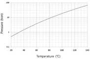
도 1은 실시예 1에서 실시한 신규한 아미노실릴아민 화합물의 증기압 측정 결과이고,
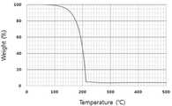
도 2는 실시예 1에서 실시한 신규한 아미노실릴아민 화합물의 열무게 분석 결과이고,
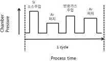
도 3은 실시예 2에서 실시한 Si-N 결합을 포함하는 절연막의 증착 방법을 나타낸 그림이고,
도 4는 실시예 3내지 5에서 실시한 Si-N 결합을 포함하는 절연막의 증착 방법을 나타낸 그림이고,
도 5는 실시예 2에서 실시한 적외선 분광기를 통하여 증착된 Si-N 결합을 포함하는 절연막을 분석한 결과이고,
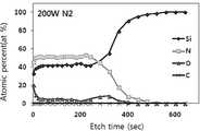
도 6은 실시예 2에서 실시한 오제 전자분광기를 통하여 증착된 Si-N 결합을 포함하는 절연막의 조성을 분석한 결과이고,
도 7은 실시예 3에서 실시한 오제 전자분광기를 통하여 증착된 Si-N 결합을 포함하는 절연막의 조성을 분석한 결과이고,
도 8은 실시예 4에서 실시한 오제 전자분광기를 통하여 증착된 Si-N 결합을 포함하는 절연막의 조성을 분석한 결과이고,
도 9은 실시예 5에서 실시한 오제 전자분광기를 통하여 증착된 Si-N 결합을 포함하는 절연막의 조성을 분석한 결과이고,
도 10은 실시예 2 내지 5 및 비교예 1 내지 2에서 실시한 Si-N 결합을 포함하는 절연막의 불화수소(300:1 BOE solution)에 대한 내성을 분석한 결과이다.Fig. 1 shows the results of vapor pressure measurement of the novel aminosilylamine compound of Example 1,
2 is a thermogravimetric analysis result of the novel aminosilylamine compound of Example 1,
3 is a view showing a method of depositing an insulating film containing Si-N bonds in Example 2. FIG.
4 is a view showing a deposition method of an insulating film containing Si-N bonds in Examples 3 to 5. FIG.
5 is a result of analyzing an insulating film containing Si-N bonds deposited through the infrared spectroscope of Example 2. FIG.
FIG. 6 is a graph showing the result of analyzing the composition of an insulating film including Si-N bonds deposited through the Eugene electron spectroscope performed in Example 2. FIG.
FIG. 7 is a result of analyzing the composition of an insulating film including a Si-N bond deposited through the Au-based electron spectroscope of Example 3,
8 is a graph showing the results of analyzing the composition of an insulating film including Si-N bonds deposited through the Au-based electron spectroscope of Example 4. FIG.
9 is a result of analyzing the composition of an insulating film including Si-N bonds deposited through the Au-based electron spectroscope performed in Example 5. FIG.
FIG. 10 shows the results of analysis of resistance to hydrogen fluoride (300: 1 BOE solution) of the insulating films including Si-N bonds in Examples 2 to 5 and Comparative Examples 1 and 2. FIG.
본 발명은 낮은 온도에서도 우수한 응집력, 높은 증착율, 물리적 특성 및 전기적 특성이 우수한 Si-N 결합을 포함하는 절연막을 형성할 수 있는 신규한 아미노실릴아민 화합물 및 이를 이용한 절연막의 제조방법을 제공한다.The present invention provides a novel aminosilylamine compound capable of forming an insulating film containing Si-N bonds with excellent cohesive strength, high deposition rate, physical properties and electrical characteristics even at low temperatures, and a method for producing an insulating film using the same.
본 발명에 따른, 상기 아미노실릴아민 화합물은 하기 화학식 1로 표시될 수 있다.The aminosilylamine compound according to the present invention may be represented by the following general formula (1).
[화학식 1][Chemical Formula 1]

[상기 화학식 1에서,[In the above formula (1)
R1 내지 R4는 서로 독립적으로 수소, (C1~C3)알킬, (C2-C3)알케닐, (C2-C3)알키닐, (C3-C7)시클로알킬 또는 (C6-C12)아릴이다.]R1 to R4 are independently of each other hydrogen, (C 1 -C 3) alkyl, (C 2 -C 3) alkenyl, (C 2 -C 3) alkynyl, (C 3 -C 7) cycloalkyl or (C 6 -C 12) aryl. ]
본 발명에 기재된 「알킬」및 그 외 「알킬」부분을 포함하는 치환체는 직쇄 또는 분쇄 형태를 모두 포함한다. 또한 본 발명에 기재된 「아릴」은 하나의 수소 제거에 의해서 방향족 탄화수소로부터 유도된 유기 라디칼로, 각 고리에 적절하게는 4 내지 7개, 바람직하게는 5 또는 6개의 고리원자를 포함하는 단일 또는 융합 고리계를 포함하며, 다수개의 아릴이 단일결합으로 연결되어 있는 형태까지 포함한다. 구체적인 예로 페닐, 나프틸, 비페닐, 안트릴, 인데닐(indenyl) 또는 플루오레닐 등을 포함하지만, 이에 한정되지 않는다. 또한 본 발명의 「알케닐」은 이중결합을 하나 이상 포함하는 직쇄 또는 분쇄형태의 탄화수소로 구체적인 예로, 바이닐, 프로프-1-엔(prop-1-ene) 또는 부타-1,3-디엔일 수 있으나, 이에 한정이 있는 것은 아니며, 본 발명의 「알키닐」은 삼중결합을 하나 이상 포함하는 직쇄 또는 분쇄형태의 탄화수소를 포함한다.The substituents comprising " alkyl " and other " alkyl " moieties described in this invention encompass both linear and branched forms. The term " aryl " in the present invention means an organic radical derived from an aromatic hydrocarbon by the removal of one hydrogen, and may be a single or fused ring containing 4 to 7, preferably 5 or 6 ring atoms, A ring system, and a form in which a plurality of aryls are connected by a single bond. Specific examples include, but are not limited to, phenyl, naphthyl, biphenyl, anthryl, indenyl, or fluorenyl. The term " alkenyl " of the present invention is a linear or branched hydrocarbon having one or more double bonds. Specific examples thereof include vinyl, prop-1-ene or buta- But the present invention is not limited thereto. The " alkynyl " of the present invention includes linear or branched hydrocarbon having at least one triple bond.
본 발명의 신규한 아미노실릴아민 화합물은 상온 및 상압하에서 액체 상태의 화합물로 뛰어난 휘발성을 가져 절연막 제조시, 증착 속도가 빠르고 용이하며, 뛰어난 응집력과 우수한 스텝커버리지를 가질 수 있다.The novel aminosilylamine compound of the present invention is a liquid compound at room temperature and atmospheric pressure and has excellent volatility, so that the deposition rate can be fast and easy, and excellent cohesion and excellent step coverage can be obtained in the production of an insulating film.
뿐만 아니라, 본 발명에 따른 아미노실릴아민 화합물은 중심 질소 원자에 3개의 실리콘 원자가 결합되어 있는 삼각 평면 Si3N 분자 구조 형태로 기인하여, 높은 열적 안정성과 낮은 활성화 에너지를 가지며, 반응성이 뛰어나고 비휘발성인 부생성물을 생성하지 않아 높은 순도의 실리콘 함유 절연막을 용이하게 형성할 수 있다는 장점을 가진다.In addition, the aminosilylamine compound according to the present invention has high thermal stability and low activation energy due to the triangular plane Si3 N molecular structure in which three silicon atoms are bonded to a central nitrogen atom, and is excellent in reactivity and nonvolatile There is an advantage that a silicon-containing insulating film of high purity can be easily formed without generating a phosphorous product.
본 발명의 일 실시예에 따른 상기 화학식 1로 표시되는 아미노실릴아민 화합물은 높은 열적 안정성과 반응성, 높은 순도의 절연막을 형성하기 위한 측면에서 바람직하게는 상기 화학식 1에서 상기 R1 내지 R4는 서로 독립적으로 수소, 메틸 또는 바이닐(vinyl) 일 수 있다.The aminosilylamine compound represented by the formula (1) according to an embodiment of the present invention is preferably a compound represented by the formula (1) wherein R1 to R4 are the same or different from each other in terms of forming an insulating film having high thermal stability, Independently, hydrogen, methyl or vinyl.

또한 뛰어난 응집력과 우수한 스텝커버리지를 가지는 절연막을 형성하기 위한 측면에서, 보다 바람직하게 상기 화학식 1은 하기 화합물에서 선택될 수 있으나, 이에 한정이 있는 것은 아니다.Further, from the viewpoint of forming an insulating film having excellent cohesion and excellent step coverage, the above-mentioned
또한 본 발명은 낮은 온도에서도 우수한 응집력, 높은 증착율, 우수한 물리적 특성 및 전기적 특성을 가지는 실리콘 박막을 형성할 수 있는 하기 화학식 2로 표시되는 아미노실릴아민 화합물을 포함하는 실릴콘 함유 절연막 증착용 조성물로 제공한다.The present invention also provides a composition for forming a silyl-cone-containing insulating film containing an aminosilylamine compound represented by the following formula (2) capable of forming a silicon thin film having excellent cohesion, high deposition rate, excellent physical properties and electrical characteristics even at low temperatures do.
[화학식 2](2)

[상기 화학식 2에서,[In the formula (2)
R1 내지 R7은 서로 독립적으로 수소, (C1~C4)알킬, (C2-C4)알케닐, (C2-C4)알키닐, (C3-C10)시클로알킬 또는 (C6-C12)아릴이다.]R1 to R7 are independently of each other hydrogen, (C 1 -C 4) alkyl, (C 2 -C 4) alkenyl, (C 2 -C 4) alkynyl, (C 3 -C 10) cycloalkyl or (C 6 -C 12) aryl. ]
본 발명에 따른 실릴콘 함유 절연막 증착용 조성물은 상기 화학식 2로 표시되는 아미노실릴아민 화합물을 절연막 증착용 전구체로 포함할 수 있으며, 상기 아미노실릴아민 화합물의 조성물 내 함량은 절연막의 성막조건, 절연막의 두께 및 특성 등을 고려하여 당업자가 인식할 수 있는 범위내로 포함될 수 있다.The silyl-cone-containing insulating film deposition composition according to the present invention may contain the aminosilylamine compound represented by Formula 2 as a precursor for forming an insulating film. The content of the aminosilylamine compound in the composition may vary depending on deposition conditions of the insulating film, May be included within a range that can be recognized by those skilled in the art in consideration of thickness, characteristics, and the like.
상기 실릴콘 함유 절연막 증착용 조성물은 절연막 증착용 전구체로 포함되는 상기 아미노실릴아민 화합물에 있어서, 습윤 에칭률을 낮추기 위한 측면에서, 바람직하게 하기 화합물에서 선택될 수 있으나, 이에 한정이 있는 것은 아니다.The silyl-cone-containing insulating film deposition composition may be selected from the following compounds in view of lowering the wet etching rate of the aminosilylamine compound, which is included as a precursor for depositing an insulating film, but is not limited thereto.


본 발명은 상기 절연막 증착용 조성물을 이용한 Si-N 결합을 포함하는 절연막의 제조방법을 제공한다.The present invention provides a method of manufacturing an insulating film including Si-N bonds using the insulating film deposition composition.
상기 절연막의 제조방법은 a) 기판에 상기 절연막 증착용 조성물을 접촉시켜 상기 기판에 흡착시키는 단계; b) 잔류 절연막 증착용 조성물 및 부산물을 퍼지하는 단계; c) 상기 절연막 증착용 조성물이 흡착된 기판에 반응가스를 주입하여 상기 절연막 증착용 조성물의 리간드를 제거함으로써, Si-N 결합의 원자층을 형성시키는 단계; 및 d) 잔류 반응가스 및 반응 부산물을 퍼지하는 단계; 를 포함할 수 있다.A) contacting the substrate with the insulating film deposition composition and adsorbing the composition on the substrate; b) purging the residual insulation film deposition composition and by-products; c) forming an atomic layer of a Si-N bond by injecting a reactive gas into the substrate on which the insulating film deposition composition has been adsorbed to remove the ligand of the insulating film deposition composition; And d) purging the residual reaction gas and reaction byproducts; . ≪ / RTI >
또한 상기 절연막의 제조방법은 a) 기판에 상기 절연막 증착용 조성물을 접촉시켜 상기 기판에 흡착시키는 단계; b) 잔류 절연막 증착용 조성물 및 부산물을 퍼지하는 단계; c‘) 반응가스를 주입하면서 플라즈마를 발생시켜 흡착된 상기 절연막 증착용 조성물의 리간드를 제거함으로써, Si-N 결합의 원자층을 형성시키는 단계; 및 d) 잔류 반응가스 및 반응 부산물을 퍼지하는 단계; 를 포함할 수 있다.The method may further comprise the steps of: a) contacting the substrate with the insulating film deposition composition and adsorbing the composition on the substrate; b) purging the residual insulation film deposition composition and by-products; forming an atomic layer of a Si-N bond by removing a ligand of the adsorbed insulation film deposition composition by generating a plasma while injecting a c ') reaction gas; And d) purging the residual reaction gas and reaction byproducts; . ≪ / RTI >
상기 절연막의 제조방법은 비활성 분위기에서 수행되는 것이 바람직하다. 또한, 높은 순도의 절연막을 제조하기 위해, 상기 a) 단계 진행 후 기판에 흡착하지 않은 여분의 아미노실릴아민 화합물 및 흡착 과정에서 생성된 부 생성물을 제거하는 단계를 더 포함 할 수 있다.The method of manufacturing the insulating film is preferably performed in an inert atmosphere. Further, in order to produce an insulating film of high purity, it may further include removing the excess aminosilylamine compound not adsorbed on the substrate and the byproducts generated in the adsorption process after the step a).
상기 c‘) 상기 반응가스를 주입하면서 플라즈마를 발생시켜 흡착된 상기 절연막 증착용 조성물의 리간드를 제거함으로써, Si-N 결합의 원자층을 형성시키는 단계; 에서는, 챔버 내에 반응 가스를 주입하고 플라즈마를 이용하여 활성화 시킨 반응가스 중 적어도 하나 이상의 반응가스 라디칼을 생성하고, 상기 활성화된 반응가스 라디칼에 의해 흡착된 상기 아미노실릴아민 화합물을 질소화(SiN), 탄질소화(SiCN) 또는 산질소화(SiON)한 후 Si-N 결합을 포함하는 절연막을 기판 위에 증착시키는 공정과, 상기 아미노실릴아민 화합물의 질소화(SiN), 탄질소화(SiCN) 또는 산질소화(SiON) 과정에서 생성되는 상기 절연막 증착용 조성물의 리간드를 제거하는 공정을 포함할 수 있다.Forming an atomic layer of a Si-N bond by removing the ligand of the adsorbed insulation film deposition composition by generating a plasma while injecting the c ') reaction gas; (SiN), nitrogen (SiN), or nitrogen (NH)) is adsorbed by the activated reaction gas radical, and at least one of the reactant gas radicals is activated by plasma, (SiN), carbonitride (SiCN), or oxynitride (SiON), followed by depositing an insulating film containing Si-N bond on the substrate after the carbonitride (SiCN) And removing the ligand of the insulating film deposition composition generated in the SiON process.
또한 목적하는 상기 Si-N 결합의 원자층의 두께가 달성될 때까지 사이클이 반복 수행될 수 있다.The cycle may also be repeated until the desired atomic layer thickness of the Si-N bond is achieved.
상기 기판의 온도는 100 내지 600℃에서 수행될 수 있으며, 바람직하게는 100 내지 550℃에서 수행되는 것이 좋다. 이는 휘발성이 우수한 상기 아미노실릴아민 화합물을 이용함으로써, 저온 공정으로도 원자층 형성이 가능함을 의미한다.The temperature of the substrate may be 100 ° C to 600 ° C, preferably 100 ° C to 550 ° C. This means that by using the aminosilylamine compound having excellent volatility, atomic layer formation is possible even at a low temperature process.
상기 원자층 형성시의 압력은 0.05 내지 30torr일 수 있으며, 바람직하게는 a) 단계는 0.05 내지 10torr의 압력일 수 있고, c) 단계 및 c‘) 단계는 0.05내지 30torr의 압력이 좋다.The pressure during formation of the atomic layer may be 0.05 to 30 torr, preferably a) may be a pressure of 0.05 to 10 torr, and steps c) and c ') may be performed at a pressure of 0.05 to 30 torr.
상기 기판의 온도는 100℃ 내지 600℃에서 수행될 수 있으며, 상기 반응가스는 질소(N2), 암모니아(NH3), N2O, NO 및 NO2 중에서 선택된 하나 이상의 질소원 반응가스일 수 있으나 이에 한정이 있는 것은 아니다. 이때, 상기 반응가스는 100 내지 10000sccm(standard cubic centimeter per minute)의 유량으로 공급되는 것이 바람직하며, 상기 c') 단계에서의 플라즈마는 50 내지 1000W의 범위로 발생시켜 활성화 시킨 후 공급되는 것이 바람직하다.The temperature of the substrate may be 100 ° C. to 600 ° C. The reaction gas may be one or more nitrogen source reactants selected from nitrogen (N2 ), ammonia (NH3 ), N2 O, NO and NO2 But is not limited thereto. At this time, it is preferable that the reaction gas is supplied at a flow rate of 100 to 10000 sccm (standard cubic centimeter per minute), and the plasma in the step c 'is preferably generated in the range of 50 to 1000 W, .
본 발명에 따른 제조방법에 의해 제조되는 절연막의 경우, 보다 낮은 온도 및 낮은 플라즈마의 공급으로도 우수한 증착율 및 고응력을 가질 수 있을 뿐 아니라 탄소 함유량을 최소화 할 수 있어 고품질의 Si-N결합을 포함하는 절연막을 형성할 수 있는 것을 특징으로 하며, 바람직하게는 50 내지 800W의 플라즈마를 발생시켜 제조될 수 있으며, 보다 바람직하게는 100 내지 500W의 낮은 플라즈마를 발생시켜 제조되는 것이 좋다.In the case of the insulating film manufactured by the manufacturing method according to the present invention, it is possible not only to have a high deposition rate and high stress even at a lower temperature and a lower plasma supply, but also to minimize the carbon content, The plasma may be generated by generating plasma of 50 to 800 W, and more preferably by generating plasma of 100 to 500 W.
또한 본 발명은 상기 아미노실릴아민 화합물을 전구체로 사용하여 제조된 Si-N결합을 포함하는 절연막을 제공한다. 상기 절연막은 본 발명에 따른 상기 아미노실릴아민 화합물을 이용함으로써, 저온에서 고응력을 가질 수 있으며, 상기 아미노실릴아민 화합물의 낮은 활성화 에너지로 인해, 증착 속도가 빠르고, 비휘발성의 부생성물이 거의 발생되지 않아 높은 순도를 가질 수 있다.The present invention also provides an insulating film containing Si-N bonds prepared using the aminosilylamine compound as a precursor. By using the aminosilylamine compound according to the present invention, the insulating film can have a high stress at a low temperature, and because of the low activation energy of the aminosilylamine compound, the deposition rate is fast and nonvolatile by- And can have high purity.
이하, 본 발명을 하기의 실시예에 의거하여 좀 더 상세히 설명하고자 한다. 단, 하기 실시예는 본 발명을 예시하기 위한 것일 뿐 한정하지는 않는다.Hereinafter, the present invention will be described in more detail based on the following examples. However, the following examples are illustrative of the present invention but are not limited thereto.
이하 모든 화합물 실시예는 글로브 박스 또는 슐랭크 관을 이용하여 무수 및 비활성 분위기 하에서 수행 하였으며, 생성물은 양성자 핵자기 공명 분광법(1H Nuclear Magnetic Resonance, NMR), 열무게 분석법(thermogravimetric analysis, TGA) 및 가스 크래마토그래피(gas chromatography, GC)를 이용하여 분석 하였으며, 증착은 상용화된 샤워헤드 방식의 200 mm 매엽식(single wafer type) ALD 장비를 사용하여 공지된 플라즈마 강화 원자층 증착법(PEALD)을 이용하여 수행하였으며, 증착한 절연막은 엘립소미터(Ellipsometer)를 하여 두께를 측정하고 적외선 분광기(infrared spectroscopy)와 오제 전자 분광기(Auger Electron Spectroscopy, AES)을 이용하여 증착된 박막 및 조성을 분석 하였다.Embodiment than all of the compounds for example by using a glove box or Schloss rank tube was performed under anhydrous and inert atmosphere, the product (thermogravimetric analysis, TGA) Proton nuclear magnetic resonance spectroscopy(1 H Nuclear Magnetic Resonance, NMR), thermogravimetric analysis and Gas chromatography (GC). The deposition was performed using a commercially available
[실시예 1] 다이메틸아미노다이메틸실릴 비스다이메틸실릴 아민 합성[Example 1] Synthesis of dimethylamino dimethylsilylbisdimethylsilylamine
무수 및 비활성 분위기 하에서 불꽃 건조된 3000mL 슐렝크 플라스크에 클로로다이메틸실란((CH3)2HSiCl) 400g(4.23mol)과 유기 용매 n-pentane 1500 ml를 넣고 교반 시키면서 암모니아(NH3) 216g(12.68mol)을 -25 ℃를 유지하면서 천천히 첨가한다. 첨가가 완료된 반응 용액을 서서히 상온으로 승온하여 6시간 교반하였다. 반응이 종료된 반응혼합물을 여과하여 생성된 흰색의 고체를 제거한 후 여과액을 얻은 후 이 여과액을 감압 하에서 용매를 제거하여, 테트라메틸다이실라잔(((CH3)2HSi)2NH) 197g 1.48mol)을 회수 하였다. 회수된 테트라메틸다이실라잔(((CH3)2HSi)2NH) 197g(1.48mol)과 유기 용매 n-hexane 300ml를 불꽃 건조된 2000 mL 슐렝크 플라스크에 넣고 교반하면서 2.29M 농도의 노말부틸리튬(n-C4H9Li) 헥산(C6H14) 용액 456g(1.48mol)을 -15℃를 유지하면서 천천히 첨가하였다. 첨가가 완료된 반응 용액을 서서히 상온으로 승온하여 12 시간 교반 시킨 후 테트라하이드로퓨란(O(C2H2)2) 500 ml를 첨가하였다. 이 반응 용액에 다이클로 다이메틸실란(Cl2Si(CH3)2)과 2 당량의 다이메틸아민을 정량적으로 반응시켜 합성한 클로로 다이메틸 다이메틸아미노실란(ClSi(CH3)2(N(CH3)2)) 203g(1.48mol)를 -20 ℃를 유지하면서 천천히 첨가하였다. 첨가가 완료된 반응 용액을 서서히 승온하여 65 ℃를 유지하면서 12 시간 교반하였다. 반응이 완료된 반응혼합물을 여과하여 생성된 흰색의 고체를 제거한 후 여과액을 얻었다. 이 여과액을 감압 하에서 용매를 제거하고, 감압 증류를 통해 다이메틸아미노다이메틸실릴 비스다이메틸실릴 아민(((CH3)2SiH)2N(Si(CH3)2(N(CH3)2)) 208g(0.89mol)을 수율 60%로 수득하였다.In a flame dried flask under dry and 3000mL Herr Lenk inert atmosphere chloro-dimethyl-silane ((CH3)2 HSiCl) while stirring into a 400g (4.23mol) with an organic solvent n-
상기 다이메틸아미노다이메틸실릴 비스다이메틸실릴 아민(((CH3)2SiH)2N(Si(CH3)2(N(CH3)2))의 증기압 및 열무게 분석을 실시하여 도 1 및 도 2에 도시하였다.The vapor pressure and thermogravimetric analysis of the above dimethylamino dimethylsilylbisdimethylsilylamine (((CH3 )2 SiH)2 N (Si (CH3 )2 (N (CH3 )2 ) And Fig.
1H-NMR(inC6D6)δ 0.20(s, 6H, NSi(CH3)2N(CH3)2), 0.23(d, 12H, NSiH(CH3)2), 2.46(s, 6H, Si(N(CH3)2), 4.68(m, 2H, NSiH(CH3)2);1 H-NMR (inC 6 D 6) δ 0.20 (s, 6H, NSi (CH 3) 2 N (CH 3) 2), 0.23 (d, 12H, NSiH (CH 3) 2), 2.46 (s, 6H, Si (N (CH 3) 2), 4.68 (m, 2H, NSiH (CH 3) 2);
끓는점 197℃;Boiling point 197 ° C;
GC 분석 결과 > 99%.GC analysis results> 99%.
[실시예 2] 플라즈마 원자층 증착법(PEALD)에 의한 Si-N 결합을 포함하는 절연막의 제조[Example 2] Preparation of insulating film containing Si-N bond by plasma atomic layer deposition (PEALD)
플라즈마 강화 원자층 증착법(PEALD)을 이용하는 통상적인 플라즈마 강화 원자층 증착(PEALD) 장치에서 실시예 1 화합물을 함유하는 절연막 증착용 조성물을 이용하여 실리콘 기판온도 300℃, 플라즈마 400W에서 Si-N 결합을 포함하는 절연막을 성막 하였다. 반응가스로는 질소(N2) 및 암모니아(NH3)를 200:30 비율로 혼합하여 사용하였고 불활성 기체인 아르곤은 퍼지 목적으로 사용하였다. 이하 도 3과 4 및 표 1에 구체적인 Si-N 결합을 포함하는 절연막의 증착 방법을 나타내었다.N-bonding at a silicon substrate temperature of 300 占 폚 and a plasma of 400 W using an insulating film deposition composition containing a compound of Example 1 in a conventional plasma enhanced atomic layer deposition (PEALD) apparatus using a plasma enhanced atomic layer deposition (PEALD) Was formed. As the reaction gas, nitrogen (N2 ) and ammonia (NH3 ) were mixed at a ratio of 200: 30, and argon, which is an inert gas, was used for purge purpose. 3 and 4 and Table 1 below show a method of depositing an insulating film containing a specific Si-N bond.
상기 실시예 2의 방법으로 증착한 Si-N 결합을 포함하는 절연막은 엘립소미터(Ellipsometer) 및 투과전자현미경(Transmission Electron Microscope. TEM)을 통하여 두께를 측정하였고, 적외선 분광기(Infrared Spectroscopy, IR), 오제 전자 분광기(Auger Electron Spectroscopy, AES) 및 이차 이온 질량 분석법(Secondary Ion Mass Spectrometer, SIMS)을 이용하여 절연막(실리콘 질화 박막)의 성분을 분석하여 하기 표 2에 나타내었다.The thickness of the insulating film including the Si-N bonds deposited by the method of Example 2 was measured by an ellipsometer and a transmission electron microscope (TEM), and an infrared spectroscopy (IR) (Silicon nitride thin film) was analyzed using Auger Electron Spectroscopy (AES) and Secondary Ion Mass Spectrometer (SIMS), and the results are shown in Table 2 below.
도 5는 적외선 분광기를, 도 6은 오제 전자 분광기를 이용하여 상기 실시예 2의 방법으로 증착한 Si-N 결합을 포함하는 절연막 및 조성을 분석한 결과를 나타내었다. 적외선 분광 스펙트럼에서 Si-N 분자 진동이 850 내지 868cm-1 범위에서 관찰되었으며, 오제 전자 분광 분석 결과 Si와 N의 비율이 0.68 내지 0.84 범위로 확인되었다. 또한 탄소 함유량은 1% 미만인 Si-N 결합을 포함하는 고품질의 절연막이 형성되었음을 알 수 있었다.FIG. 5 shows an infrared ray spectroscope, and FIG. 6 shows the results of analysis of an insulating film containing Si-N bonds and a composition thereof deposited by the method of Example 2 using an Aujee electron spectroscope. In the infrared spectroscopic spectrum, Si-N molecular vibrations were observed in the range of 850 to 868 cm-1 , and as a result of Auje analysis, the ratio of Si to N was found to be in the range of 0.68 to 0.84. It was also found that a high-quality insulating film containing Si-N bonds having a carbon content of less than 1% was formed.
[실시예 3] 플라즈마 원자층 증착법(PEALD)에 의한 Si-N 결합을 포함하는 절연막의 제조[Example 3] Fabrication of insulating film containing Si-N bond by plasma atomic layer deposition (PEALD)
플라즈마 강화 원자층 증착법(PEALD)을 이용하는 통상적인 플라즈마 강화 원자층 증착(PEALD) 장치에서 실시예 1 화합물을 함유하는 절연막 증착용 조성물을 이용하여 실리콘 기판온도 300℃, 플라즈마 100W에서 Si-N 결합을 포함하는 절연막을 성막 하였다. 반응가스로는 질소(N2)를 사용하였고 불활성 기체인 아르곤은 퍼지 목적으로 사용하였다. 이하 도 4와 표 1에 구체적인 Si-N 결합을 포함하는 절연막의 증착 방법을 나타내었다.In a conventional plasma enhanced atomic layer deposition (PEALD) apparatus using plasma enhanced atomic layer deposition (PEALD), an insulating film deposition composition containing the compound of Example 1 was used to deposit Si-N bonds at a silicon substrate temperature of 300 DEG C and a plasma of 100 W Was formed. Nitrogen (N2 ) was used as a reaction gas and argon, which is an inert gas, was used for purge purpose. 4 and Table 1 show a method of depositing an insulating film containing a specific Si-N bond.
상기 실시예 3의 방법으로 증착한 Si-N 결합을 포함하는 절연막은 상기 실시예 2의 방법과 동일하게 절연막의 성분을 분석하여 하기 표 2에 나타내었다(도 7 참조).The insulating film containing Si-N bonds deposited by the method of Example 3 was analyzed for the components of the insulating film in the same manner as in Example 2, and is shown in Table 2 below (see FIG. 7).
[실시예 4] 플라즈마 원자층 증착법(PEALD)에 의한 Si-N 결합을 포함하는 절연막의 제조[Example 4] Production of insulating film containing Si-N bond by plasma atomic layer deposition (PEALD)
플라즈마 강화 원자층 증착법(PEALD)을 이용하는 통상적인 플라즈마 강화 원자층 증착(PEALD) 장치에서 실시예 1 화합물을 함유하는 절연막 증착용 조성물을 이용하여 실리콘 기판온도 300℃, 플라즈마 200W에서 Si-N 결합을 포함하는 절연막을 성막 하였다. 반응가스로는 질소(N2)를 사용하였고 불활성 기체인 아르곤은 퍼지 목적으로 사용하였다. 이하 도 4와 표 1에 구체적인 Si-N 결합을 포함하는 절연막의 증착 방법을 나타내었다.In a conventional plasma enhanced atomic layer deposition (PEALD) apparatus using plasma enhanced atomic layer deposition (PEALD), an insulating film deposition composition containing the compound of Example 1 was used to deposit Si-N bonds at a silicon substrate temperature of 300 DEG C and a plasma of 200W Was formed. Nitrogen (N2 ) was used as a reaction gas and argon, which is an inert gas, was used for purge purpose. 4 and Table 1 show a method of depositing an insulating film containing a specific Si-N bond.
상기 실시예 4의 방법으로 증착한 Si-N 결합을 포함하는 절연막은 상기 실시예 2의 방법과 동일하게 절연막의 성분을 분석하여 하기 표 2에 나타내었다(도 8 참조).The insulating film containing Si-N bonds deposited by the method of Example 4 was analyzed for the components of the insulating film in the same manner as in Example 2, and is shown in Table 2 below (see FIG. 8).
[실시예 5] 플라즈마 원자층 증착법(PEALD)에 의한 Si-N 결합을 포함하는 절연막의 제조[Example 5] Preparation of insulating film containing Si-N bond by plasma atomic layer deposition (PEALD)
플라즈마 강화 원자층 증착법(PEALD)을 이용하는 통상적인 플라즈마 강화 원자층 증착(PEALD) 장치에서 실시예 1 화합물을 함유하는 절연막 증착용 조성물을 이용하여 실리콘 기판온도 300℃, 플라즈마 400W에서 Si-N 결합을 포함하는 절연막을 성막 하였다. 반응가스로는 질소(N2)를 사용하였고 불활성 기체인 아르곤은 퍼지 목적으로 사용하였다. 이하 도 4와 표 1에 구체적인 Si-N 결합을 포함하는 절연막의 증착 방법을 나타내었다.N-bonding at a silicon substrate temperature of 300 占 폚 and a plasma of 400 W using an insulating film deposition composition containing a compound of Example 1 in a conventional plasma enhanced atomic layer deposition (PEALD) apparatus using a plasma enhanced atomic layer deposition (PEALD) Was formed. Nitrogen (N2 ) was used as a reaction gas and argon, which is an inert gas, was used for purge purpose. 4 and Table 1 show a method of depositing an insulating film containing a specific Si-N bond.
상기 실시예 5의 방법으로 증착한 Si-N 결합을 포함하는 절연막은 상기 실시예 2의 방법과 동일하게 절연막의 성분을 분석하여 하기 표 2에 나타내었다(도 9 참조).The insulating film containing Si-N bonds deposited by the method of Example 5 was analyzed for the components of the insulating film in the same manner as in Example 2, and is shown in Table 2 below (see FIG. 9).
[비교예 1][Comparative Example 1]
저압화학기상증착방법(LPCVD)을 이용하여 기판온도 700℃, 디클로로실란(DCS) 40sccm 및 암모니아(NH3) 240sccm 조건 하에서 절연막을 제조하였다. 이하 표 1에 구체적인 절연막의 증착 방법을 나타내었으며, 상기 절연막은 상기 실시예 2의 방법과 동일하게 절연막의 성분을 분석하여 하기 표 2에 나타내었다.An insulating film was fabricated by low pressure chemical vapor deposition (LPCVD) at a substrate temperature of 700 ° C, 40 sccm of dichlorosilane (DCS), and 240 sccm of ammonia (NH3 ). Table 1 below shows a method of depositing a specific insulating film. The insulating film was analyzed for the components of the insulating film in the same manner as in Example 2, and the results are shown in Table 2 below.
[비교예 2][Comparative Example 2]
플라즈마를 이용한 화학기상증착법(PECVD)을 이용하여 기판온도 400℃, 플라즈마 500W, 실란(SiH4)과 암모니아(NH3) 비율 1:8 조건 하에서 절연막을 제조하였다. 이하 표 1에 구체적인 절연막의 증착 방법을 나타내었으며, 상기 절연막은 상기 실시예 2의 방법과 동일하게 절연막의 성분을 분석하여 하기 표 2에 나타내었다.An insulating film was prepared by plasma enhanced chemical vapor deposition (PECVD) at a substrate temperature of 400 ° C., a plasma of 500 W, and a silane (SiH4 ) and ammonia (NH3 ) ratio of 1: 8. Table 1 below shows a method of depositing a specific insulating film. The insulating film was analyzed for the components of the insulating film in the same manner as in Example 2, and the results are shown in Table 2 below.


그 결과, 본 발명에 따른 상기 Si-N 결합을 포함하는 절연막의 증착율은 0.21 내지 0.48 /cycle 범위를 가지는 것으로 나타났다.As a result, the deposition rate of the insulating film including the Si-N bond according to the present invention was found to be in the range of 0.21 to 0.48 / cycle.
또한 도 10에 도시한 바와 같이, 실시예 2 내지 5에서 제조한 Si-N 결합을 포함하는 절연막의 불화수소(300:1 BOE solution)에 대한 내성을 분석한 결과 고온에서 저압화학기상증착방법(LPCVD)을 이용하여 형성한 절연막인 비교예 1의 불화수소(300:1 BOE solution)에 대한 내성과 비교하였으며, 그 결과 2.89 내지 28.06배의 내성을 가지는 것으로, 불화수소에 대한 내성이 뛰어남을 확인할 수 있었다.Further, as shown in FIG. 10, the resistance of the insulating film containing Si-N bonds prepared in Examples 2 to 5 to hydrogen fluoride (300: 1 BOE solution) was analyzed by a low pressure chemical vapor deposition method (300: 1 BOE solution) of Comparative Example 1, which is an insulating film formed by using LPCVD (LPCVD). As a result, it has resistance of 2.89 to 28.06 times, confirming excellent resistance to hydrogen fluoride I could.
즉, 본 발명에 따라 플라즈마 원자층 증착 공정을 통하여 아미노실릴아민 화합물을 포함하는 실리콘 함유 절연막 증착용 조성물을 사용하면 저온 및 낮은 플라즈마에서 증착 가능한 고순도의 Si-N 포함된 절연막을 형성하는데 그 활용가치가 높을 것으로 확인 되었고, 실리콘 함유 절연막의 응용 전 분야에 걸쳐 유용하게 사용 될 수 있을 것으로 판단된다.That is, when a silicon-containing insulating film deposition composition containing an aminosilylamine compound is used through a plasma atomic layer deposition process according to the present invention, a high-purity Si-N-containing insulating film which can be deposited at low temperature and low plasma is formed, And it is considered that it can be usefully used throughout the application fields of the silicon-containing insulating film.
Claims (13)
Translated fromKorean[화학식 1]

[상기 화학식 1에서,
R1 및 R2중 하나는 수소 또는 (C1~C3)알킬이고, 나머지 하나는 (C1~C3)알킬이고;
R3및 R4는 서로 독립적으로 수소 또는 (C1~C3)알킬이다.]An aminosilylamine compound represented by the following formula (1):
[Chemical Formula 1]
[In the above formula (1)
One of R <1 > and R <2 > is hydrogen or (C1-C3) alkyl and the other is (C1-C3) alkyl;
R3 and R4 are independently of each other hydrogen or (C 1 -C 3) alkyl.
상기 화학식 1은 하기 화합물로부터 선택되는 것인 아미노실릴아민 화합물.

(1) is selected from the following compounds.
[화학식 2]

[상기 화학식 2에서,
R1 내지 R7은 서로 독립적으로 수소 또는 (C1~C4)알킬이되, R1, R2 및 R3가 동시에 수소인 경우는 제외된다.]A silicon-containing insulating film deposition composition comprising an aminosilylamine compound represented by the following formula (2):
(2)
[In the formula (2)
R1 to R7 independently of one another are hydrogen or (C 1 -C 4) alkyl, and R1 , R2 and R3 are simultaneously hydrogen.]
상기 화학식 2는 하기 화합물로부터 선택되는 절연막 증착용 조성물:


(2) is selected from the following compounds:
a) 기판에 상기 절연막 증착용 조성물을 접촉시켜 상기 기판에 흡착시키는 단계; b) 잔류 절연막 증착용 조성물 및 부산물을 퍼지하는 단계; c) 상기 절연막 증착용 조성물이 흡착된 기판에 반응가스를 주입하여 상기 절연막 증착용 조성물의 리간드를 제거함으로써, Si-N 결합의 원자층을 형성시키는 단계; 및 d) 잔류 반응가스 및 반응 부산물을 퍼지하는 단계; 를 포함하는 절연막을 제조하는 방법.The method according to claim 6,
a) contacting the substrate with the insulating film deposition composition and adsorbing the composition on the substrate; b) purging the residual insulation film deposition composition and by-products; c) forming an atomic layer of a Si-N bond by injecting a reactive gas into the substrate on which the insulating film deposition composition has been adsorbed to remove the ligand of the insulating film deposition composition; And d) purging the residual reaction gas and reaction byproducts; Wherein the insulating film has a thickness of 10 nm or less.
a) 기판에 상기 절연막 증착용 조성물을 접촉시켜 상기 기판에 흡착시키는 단계; b) 잔류 절연막 증착용 조성물 및 부산물을 퍼지하는 단계; c') 반응가스를 주입하면서 플라즈마를 발생시켜 흡착된 상기 절연막 증착용 조성물의 리간드를 제거함으로써, Si-N 결합의 원자층을 형성시키는 단계; 및 d) 잔류 반응가스 및 반응 부산물을 퍼지하는 단계; 를 포함하는 절연막을 제조하는 방법.The method according to claim 6,
a) contacting the substrate with the insulating film deposition composition and adsorbing the composition on the substrate; b) purging the residual insulation film deposition composition and by-products; forming an atomic layer of a Si-N bond by removing a ligand of the adsorbed insulation film deposition composition by generating a plasma while injecting a c ') reaction gas; And d) purging the residual reaction gas and reaction byproducts; Wherein the insulating film has a thickness of 10 nm or less.
상기 반응가스는 50 내지 1000W의 플라즈마를 발생시켜 활성화 시킨 후 공급하여 절연막을 제조하는 방법.9. The method according to any one of claims 7 and 8,
Wherein the reaction gas is generated by activating plasma of 50 to 1000 W, and then supplied to supply the activated gas.
상기 반응가스는 100 내지 500W의 플라즈마를 발생시켜 활성화 시킨 후 공급하여 절연막을 제조하는 방법.10. The method of claim 9,
Wherein the reaction gas is generated by activating a plasma of 100 to 500 W and then supplied to activate the plasma.
상기 기판의 온도는 100 내지 600℃에서 수행되는 것인 절연막을 제조하는 방법.11. The method of claim 10,
Wherein the temperature of the substrate is performed at 100 to 600 占 폚.
상기 반응가스는 100 내지 10000sccm의 유량으로 공급하는 것인 절연막을 제조하는 방법.11. The method of claim 10,
Wherein the reaction gas is supplied at a flow rate of 100 to 10000 sccm.
a) 단계는 0.05 내지 10torr의 압력에서 수행되고, c) 단계 및 c') 단계는 0.05 내지 30torr의 압력에서 수행되는 것인 절연막을 제조하는 방법.11. The method of claim 10,
wherein step a) is carried out at a pressure of 0.05 to 10 torr, and steps c) and c ') are carried out at a pressure of 0.05 to 30 torr.
Priority Applications (4)
| Application Number | Priority Date | Filing Date | Title |
|---|---|---|---|
| US15/317,920US9916974B2 (en) | 2014-06-11 | 2015-06-04 | Amino-silyl amine compound and the manufacturing method of dielectric film containing Si—N bond by using atomic layer deposition |
| CN201580030728.1ACN106488924B (en) | 2014-06-11 | 2015-06-04 | Novel amino-silylamine compounds and methods for making dielectric films containing Si-N bonds by using atomic layer deposition |
| PCT/KR2015/005610WO2015190749A1 (en) | 2014-06-11 | 2015-06-04 | Novel amino-silyl amine compound and the manufacturing method of dielectric film containing si-n bond by using atomic layer deposition |
| JP2016568508AJP6343032B2 (en) | 2014-06-11 | 2015-06-04 | Novel aminosilylamine compound and method for producing insulating film containing Si-N bond using atomic layer deposition method |
Applications Claiming Priority (2)
| Application Number | Priority Date | Filing Date | Title |
|---|---|---|---|
| KR1020140070909 | 2014-06-11 | ||
| KR20140070909 | 2014-06-11 |
Publications (2)
| Publication Number | Publication Date |
|---|---|
| KR20150142591A KR20150142591A (en) | 2015-12-22 |
| KR101875183B1true KR101875183B1 (en) | 2018-07-06 |
Family
ID=55081850
Family Applications (1)
| Application Number | Title | Priority Date | Filing Date |
|---|---|---|---|
| KR1020150069444AActiveKR101875183B1 (en) | 2014-06-11 | 2015-05-19 | Novel amino-silyl amine compound and the manufacturing method of dielectric film containing Si-N bond by using atomic layer deposition |
Country Status (4)
| Country | Link |
|---|---|
| US (1) | US9916974B2 (en) |
| JP (1) | JP6343032B2 (en) |
| KR (1) | KR101875183B1 (en) |
| CN (1) | CN106488924B (en) |
Families Citing this family (9)
| Publication number | Priority date | Publication date | Assignee | Title |
|---|---|---|---|---|
| US9777025B2 (en)* | 2015-03-30 | 2017-10-03 | L'Air Liquide, Société pour l'Etude et l'Exploitation des Procédés Georges Claude | Si-containing film forming precursors and methods of using the same |
| WO2018016871A1 (en)* | 2016-07-22 | 2018-01-25 | (주)디엔에프 | Method for manufacturing silicon nitride thin film using plasma atomic layer deposition |
| KR102014175B1 (en)* | 2016-07-22 | 2019-08-27 | (주)디엔에프 | The manufacturing method of the silicon nitride film by using plasma enhanced atomic layer deposition |
| KR20180110612A (en)* | 2017-03-29 | 2018-10-10 | (주)디엔에프 | Compositions for depositing silicon-containing thin films containing bis(aminosilyl)alkylamine compound and methods for manufacturing silicon-containing thin film using the same |
| US11049714B2 (en)* | 2017-09-19 | 2021-06-29 | Versum Materials Us, Llc | Silyl substituted organoamines as precursors for high growth rate silicon-containing films |
| US10927459B2 (en) | 2017-10-16 | 2021-02-23 | Asm Ip Holding B.V. | Systems and methods for atomic layer deposition |
| KR102190532B1 (en)* | 2017-11-22 | 2020-12-15 | (주)디엔에프 | Composition for silicon-containing thin films and method for producing silicon-containing thin film |
| EP4146725B1 (en)* | 2020-05-07 | 2024-05-22 | Merck Patent GmbH | Polycarbosilazane, and composition comprising the same, and method for producing silicon-containing film using the same |
| CN117642525A (en)* | 2021-07-16 | 2024-03-01 | Up化学株式会社 | Silicon precursor compound, composition for forming silicon-containing film comprising the same, and method for forming film using composition for forming silicon-containing film |
Citations (5)
| Publication number | Priority date | Publication date | Assignee | Title |
|---|---|---|---|---|
| JP3088540B2 (en)* | 1991-02-01 | 2000-09-18 | プリファ・アグロ・ホールディング・ベスローテン・フェンノートシャップ | Preparation of membranes for electrochemical or optical sensors |
| US20090087561A1 (en)* | 2007-09-28 | 2009-04-02 | Advanced Technology Materials, Inc. | Metal and metalloid silylamides, ketimates, tetraalkylguanidinates and dianionic guanidinates useful for cvd/ald of thin films |
| KR20110132534A (en)* | 2010-06-02 | 2011-12-08 | 에어 프로덕츠 앤드 케미칼스, 인코오포레이티드 | Organoaminosilane precursor and method for depositing a film comprising the same |
| KR101149811B1 (en)* | 2010-11-17 | 2012-07-19 | 주식회사 유피케미칼 | Deposition method of thin film using silicon precursor |
| KR20130135793A (en)* | 2012-06-01 | 2013-12-11 | 에어 프로덕츠 앤드 케미칼스, 인코오포레이티드 | Organoaminodisilane precursors and methods for depositing films comprising same |
Family Cites Families (8)
| Publication number | Priority date | Publication date | Assignee | Title |
|---|---|---|---|---|
| DE1158972B (en)* | 1961-03-25 | 1963-12-12 | Franz Josef Carduck Dipl Chem | Process for the preparation of trisilylamines |
| US5413813A (en)* | 1993-11-23 | 1995-05-09 | Enichem S.P.A. | CVD of silicon-based ceramic materials on internal surface of a reactor |
| JP2004281853A (en) | 2003-03-18 | 2004-10-07 | Hitachi Kokusai Electric Inc | Substrate processing equipment |
| US7119016B2 (en)* | 2003-10-15 | 2006-10-10 | International Business Machines Corporation | Deposition of carbon and nitrogen doped poly silicon films, and retarded boron diffusion and improved poly depletion |
| JP4607637B2 (en) | 2005-03-28 | 2011-01-05 | 東京エレクトロン株式会社 | Silicon nitride film forming method, silicon nitride film forming apparatus and program |
| JP6022166B2 (en) | 2011-02-28 | 2016-11-09 | 株式会社日立国際電気 | Semiconductor device manufacturing method, substrate processing apparatus, and program |
| WO2013177326A1 (en) | 2012-05-25 | 2013-11-28 | Advanced Technology Materials, Inc. | Silicon precursors for low temperature ald of silicon-based thin-films |
| US10421766B2 (en)* | 2015-02-13 | 2019-09-24 | Versum Materials Us, Llc | Bisaminoalkoxysilane compounds and methods for using same to deposit silicon-containing films |
- 2015
- 2015-05-19KRKR1020150069444Apatent/KR101875183B1/enactiveActive
- 2015-06-04CNCN201580030728.1Apatent/CN106488924B/enactiveActive
- 2015-06-04USUS15/317,920patent/US9916974B2/enactiveActive
- 2015-06-04JPJP2016568508Apatent/JP6343032B2/enactiveActive
Patent Citations (5)
| Publication number | Priority date | Publication date | Assignee | Title |
|---|---|---|---|---|
| JP3088540B2 (en)* | 1991-02-01 | 2000-09-18 | プリファ・アグロ・ホールディング・ベスローテン・フェンノートシャップ | Preparation of membranes for electrochemical or optical sensors |
| US20090087561A1 (en)* | 2007-09-28 | 2009-04-02 | Advanced Technology Materials, Inc. | Metal and metalloid silylamides, ketimates, tetraalkylguanidinates and dianionic guanidinates useful for cvd/ald of thin films |
| KR20110132534A (en)* | 2010-06-02 | 2011-12-08 | 에어 프로덕츠 앤드 케미칼스, 인코오포레이티드 | Organoaminosilane precursor and method for depositing a film comprising the same |
| KR101149811B1 (en)* | 2010-11-17 | 2012-07-19 | 주식회사 유피케미칼 | Deposition method of thin film using silicon precursor |
| KR20130135793A (en)* | 2012-06-01 | 2013-12-11 | 에어 프로덕츠 앤드 케미칼스, 인코오포레이티드 | Organoaminodisilane precursors and methods for depositing films comprising same |
Also Published As
| Publication number | Publication date |
|---|---|
| JP6343032B2 (en) | 2018-06-13 |
| US20170125243A1 (en) | 2017-05-04 |
| US9916974B2 (en) | 2018-03-13 |
| KR20150142591A (en) | 2015-12-22 |
| CN106488924A (en) | 2017-03-08 |
| JP2017518286A (en) | 2017-07-06 |
| CN106488924B (en) | 2019-06-21 |
Similar Documents
| Publication | Publication Date | Title |
|---|---|---|
| KR101875183B1 (en) | Novel amino-silyl amine compound and the manufacturing method of dielectric film containing Si-N bond by using atomic layer deposition | |
| JP6456450B2 (en) | Novel cyclodisilazane derivative, production method thereof, and silicon-containing thin film using the same | |
| JP6018125B2 (en) | Novel aminosilylamine compound, method for producing the same, and silicon-containing thin film using the same | |
| KR101857478B1 (en) | Novel trisilyl amine derivative, method for manufacturing thereof and silicon-containing thin film use the same | |
| JP6876145B2 (en) | A composition for vapor deposition of a silicon-containing thin film containing a bis (aminosilyl) alkylamine compound, and a method for producing a silicon-containing thin film using the composition. | |
| KR20170019668A (en) | The manufacturing method of the silicon nitride film by using plasma enhanced atomic layer deposition | |
| JP6923994B2 (en) | Silicon-containing thin film deposition composition and method for producing silicon-containing thin film using it | |
| US11142462B2 (en) | Trichlorodisilane | |
| KR102005940B1 (en) | Novel amino-silyl amine compound, method for manufacturing thereof and silicon-containing thin film use the same | |
| CN109790036B (en) | Chlorodisilazane | |
| WO2015190749A1 (en) | Novel amino-silyl amine compound and the manufacturing method of dielectric film containing si-n bond by using atomic layer deposition | |
| KR101934773B1 (en) | Low temperature process for forming a silicon-containing thin layer | |
| KR101770718B1 (en) | Silicon precursor and manufacturing method of silicon-containing thin film using thereof | |
| TW202311273A (en) | Silicon precursors |
Legal Events
| Date | Code | Title | Description |
|---|---|---|---|
| PA0109 | Patent application | Patent event code:PA01091R01D Comment text:Patent Application Patent event date:20150519 | |
| PG1501 | Laying open of application | ||
| A201 | Request for examination | ||
| PA0201 | Request for examination | Patent event code:PA02012R01D Patent event date:20160630 Comment text:Request for Examination of Application Patent event code:PA02011R01I Patent event date:20150519 Comment text:Patent Application | |
| E902 | Notification of reason for refusal | ||
| PE0902 | Notice of grounds for rejection | Comment text:Notification of reason for refusal Patent event date:20170920 Patent event code:PE09021S01D | |
| E701 | Decision to grant or registration of patent right | ||
| PE0701 | Decision of registration | Patent event code:PE07011S01D Comment text:Decision to Grant Registration Patent event date:20180419 | |
| PR0701 | Registration of establishment | Comment text:Registration of Establishment Patent event date:20180629 Patent event code:PR07011E01D | |
| PR1002 | Payment of registration fee | Payment date:20180702 End annual number:3 Start annual number:1 | |
| PG1601 | Publication of registration | ||
| PR1001 | Payment of annual fee | Payment date:20210602 Start annual number:4 End annual number:4 | |
| PR1001 | Payment of annual fee | Payment date:20220325 Start annual number:5 End annual number:5 | |
| PR1001 | Payment of annual fee | Payment date:20230314 Start annual number:6 End annual number:6 | |
| PR1001 | Payment of annual fee | Payment date:20240319 Start annual number:7 End annual number:7 | |
| PR1001 | Payment of annual fee | Payment date:20250317 Start annual number:8 End annual number:8 |