KR101874106B1 - Method of driving display panel and display apparatus for performing the same - Google Patents
Method of driving display panel and display apparatus for performing the sameDownload PDFInfo
- Publication number
- KR101874106B1 KR101874106B1KR1020110017890AKR20110017890AKR101874106B1KR 101874106 B1KR101874106 B1KR 101874106B1KR 1020110017890 AKR1020110017890 AKR 1020110017890AKR 20110017890 AKR20110017890 AKR 20110017890AKR 101874106 B1KR101874106 B1KR 101874106B1
- Authority
- KR
- South Korea
- Prior art keywords
- data
- pixel
- gate line
- storage
- voltage
- Prior art date
- Legal status (The legal status is an assumption and is not a legal conclusion. Google has not performed a legal analysis and makes no representation as to the accuracy of the status listed.)
- Expired - Fee Related
Links
Images


Classifications
- G—PHYSICS
- G09—EDUCATION; CRYPTOGRAPHY; DISPLAY; ADVERTISING; SEALS
- G09G—ARRANGEMENTS OR CIRCUITS FOR CONTROL OF INDICATING DEVICES USING STATIC MEANS TO PRESENT VARIABLE INFORMATION
- G09G3/00—Control arrangements or circuits, of interest only in connection with visual indicators other than cathode-ray tubes
- G09G3/20—Control arrangements or circuits, of interest only in connection with visual indicators other than cathode-ray tubes for presentation of an assembly of a number of characters, e.g. a page, by composing the assembly by combination of individual elements arranged in a matrix no fixed position being assigned to or needed to be assigned to the individual characters or partial characters
- G09G3/34—Control arrangements or circuits, of interest only in connection with visual indicators other than cathode-ray tubes for presentation of an assembly of a number of characters, e.g. a page, by composing the assembly by combination of individual elements arranged in a matrix no fixed position being assigned to or needed to be assigned to the individual characters or partial characters by control of light from an independent source
- G09G3/36—Control arrangements or circuits, of interest only in connection with visual indicators other than cathode-ray tubes for presentation of an assembly of a number of characters, e.g. a page, by composing the assembly by combination of individual elements arranged in a matrix no fixed position being assigned to or needed to be assigned to the individual characters or partial characters by control of light from an independent source using liquid crystals
- G09G3/3611—Control of matrices with row and column drivers
- G09G3/3648—Control of matrices with row and column drivers using an active matrix
- G09G3/3655—Details of drivers for counter electrodes, e.g. common electrodes for pixel capacitors or supplementary storage capacitors
- G—PHYSICS
- G09—EDUCATION; CRYPTOGRAPHY; DISPLAY; ADVERTISING; SEALS
- G09G—ARRANGEMENTS OR CIRCUITS FOR CONTROL OF INDICATING DEVICES USING STATIC MEANS TO PRESENT VARIABLE INFORMATION
- G09G2310/00—Command of the display device
- G09G2310/02—Addressing, scanning or driving the display screen or processing steps related thereto
- G09G2310/0202—Addressing of scan or signal lines
- G09G2310/0205—Simultaneous scanning of several lines in flat panels
- G—PHYSICS
- G09—EDUCATION; CRYPTOGRAPHY; DISPLAY; ADVERTISING; SEALS
- G09G—ARRANGEMENTS OR CIRCUITS FOR CONTROL OF INDICATING DEVICES USING STATIC MEANS TO PRESENT VARIABLE INFORMATION
- G09G2310/00—Command of the display device
- G09G2310/02—Addressing, scanning or driving the display screen or processing steps related thereto
- G09G2310/0243—Details of the generation of driving signals
- G09G2310/0251—Precharge or discharge of pixel before applying new pixel voltage
- G—PHYSICS
- G09—EDUCATION; CRYPTOGRAPHY; DISPLAY; ADVERTISING; SEALS
- G09G—ARRANGEMENTS OR CIRCUITS FOR CONTROL OF INDICATING DEVICES USING STATIC MEANS TO PRESENT VARIABLE INFORMATION
- G09G2320/00—Control of display operating conditions
- G09G2320/02—Improving the quality of display appearance
- G09G2320/0257—Reduction of after-image effects
- G—PHYSICS
- G09—EDUCATION; CRYPTOGRAPHY; DISPLAY; ADVERTISING; SEALS
- G09G—ARRANGEMENTS OR CIRCUITS FOR CONTROL OF INDICATING DEVICES USING STATIC MEANS TO PRESENT VARIABLE INFORMATION
- G09G2320/00—Control of display operating conditions
- G09G2320/02—Improving the quality of display appearance
- G09G2320/0271—Adjustment of the gradation levels within the range of the gradation scale, e.g. by redistribution or clipping
- G—PHYSICS
- G09—EDUCATION; CRYPTOGRAPHY; DISPLAY; ADVERTISING; SEALS
- G09G—ARRANGEMENTS OR CIRCUITS FOR CONTROL OF INDICATING DEVICES USING STATIC MEANS TO PRESENT VARIABLE INFORMATION
- G09G2340/00—Aspects of display data processing
- G09G2340/16—Determination of a pixel data signal depending on the signal applied in the previous frame
Landscapes
- Engineering & Computer Science (AREA)
- Chemical & Material Sciences (AREA)
- Crystallography & Structural Chemistry (AREA)
- Physics & Mathematics (AREA)
- Computer Hardware Design (AREA)
- General Physics & Mathematics (AREA)
- Theoretical Computer Science (AREA)
- Power Engineering (AREA)
- Liquid Crystal Display Device Control (AREA)
- Control Of Indicators Other Than Cathode Ray Tubes (AREA)
- Liquid Crystal (AREA)
Abstract
Translated fromKoreanDescription
Translated fromKorean본 발명은 표시 패널의 구동 방법 및 이를 수행하기 위한 표시 장치에 관한 것으로, 보다 상세하게는 표시 품질을 향상시키기 위한 표시 패널의 구동 방법 및 이를 수행하기 위한 표시 장치에 관한 것이다.BACKGROUND OF THE
일반적으로, 액정 표시 장치는 화소 전극을 포함하는 제1 기판, 공통 전극을 포함하는 제2 기판 및 상기 기판들 사이에 개재되는 액정층을 포함한다. 상기 두 전극에 전압을 인가하여 액정층에 전계를 생성하고, 이 전계의 세기를 조절하여 액정층을 통과하는 빛의 투과율을 조절함으로써 원하는 화상을 얻는다.Generally, a liquid crystal display device includes a first substrate including a pixel electrode, a second substrate including a common electrode, and a liquid crystal layer interposed between the substrates. A voltage is applied to the two electrodes to generate an electric field in the liquid crystal layer, and the intensity of the electric field is adjusted to adjust the transmittance of light passing through the liquid crystal layer to obtain a desired image.
회로 상의 딜레이로 인해 상기 화소 전극에는 원하는 데이터 전압이 충전되지 않을 수 있다. 상기 화소 전극에 인가되는 데이터 전압의 충전량을 보상하기 위해 게이트 신호의 인가 시간을 1 수평 주기 보다 길게 조절하는 프리차지 구동 방식이 채용되고 있다.The desired data voltage may not be charged to the pixel electrode due to a delay in the circuit. A precharge driving method is adopted in which the application time of the gate signal is adjusted to be longer than one horizontal period in order to compensate the charged amount of the data voltage applied to the pixel electrode.
데이터 라인에 연결되는 화소들은 표시 영상에 대응하여 고 계조를 나타내기도 하고 저 계조를 나타내기도 한다. 상기 프리차지 구동에서 하나의 데이터 라인에 연결된 화소들이 저 계조 후에 고 계조를 표시하면, 상기 화소 전극에는 저 계조의 데이터 전압이 프리차지되어 상기 고 계조를 표시할 때 데이터 전압의 충전률을 보상할 수 있다.The pixels connected to the data line may correspond to a display image and display a high gray level or a low gray level. When pixels connected to one data line in the precharge driving display display a high gray scale after a low gray scale, a data voltage of a low gray scale is precharged to the pixel electrode and a charging rate of the data voltage is compensated .
그러나, 상기 프리차지 구동에서 하나의 데이터 라인에 연결된 화소들이 고 계조 후에 저 계조를 표시하면, 상기 저 계조에 대응하는 화소 전극에 프리차지된 고 계조의 데이터 전압이 상기 딜레이로 인해 충분히 방전되지 않아, 상기 저 계조에 대응하는 화소 전극에는 원하는 데이터 전압보다 높은 데이터 전압이 충전될 수 있다. 따라서, 상기 저 계조에 대응하는 화소는 원하는 계조보다 높은 계조를 표시하게 되는 문제점이 있다. 이러한 현상을 고스트(ghost)라고 한다.However, if the pixels connected to one data line in the precharge driving display display a low gray scale after a high gray scale, the high gray scale data voltage precharged to the pixel electrode corresponding to the low gray scale is not sufficiently discharged due to the delay , A data voltage higher than a desired data voltage can be charged to the pixel electrode corresponding to the low gray level. Therefore, the pixels corresponding to the low gradations display grayscales higher than the desired gradations. This phenomenon is called ghost.
예를 들어, 상기 고스트는 적색 화소가 고 계조를 표시하고 상기 적색 화소와 동일한 데이터 라인에 연결된 바로 다음의 녹색 화소가 저 계조를 표시할 때 사용자에게 잘 시인된다.For example, the ghost is well visible to the user when the red pixel indicates a high gradation and the next green pixel connected to the same data line as the red pixel indicates a low gradation.
상기 고스트로 인해 표시 패널의 표시 품질이 저하되는 문제점이 있다.There is a problem that the display quality of the display panel deteriorates due to the ghost.
이에 본 발명의 기술적 과제는 이러한 점에 착안한 것으로, 본 발명의 목적은 표시 품질을 향상시키기 위한 표시 패널의 구동 방법을 제공하는 것이다.SUMMARY OF THE INVENTION Accordingly, the present invention has been made keeping in mind the above problems occurring in the prior art, and it is an object of the present invention to provide a method of driving a display panel for improving display quality.
본 발명의 다른 목적은 상기 구동 방법을 수행하기 위한 표시 장치를 제공하는 것이다.Another object of the present invention is to provide a display device for performing the driving method.
상기한 본 발명의 목적을 실현하기 위한 일 실시예에 따른 표시 패널의 구동 방법은 제N 게이트 라인에 대응하는 계조 데이터를 증가시켜 보정 계조 데이터를 생성하는 단계, 상기 보정 계조 데이터를 기초로 데이터 전압을 생성하여 표시 패널에 출력하는 단계, 제1 레벨 및 상기 제1 레벨보다 낮은 제2 레벨을 갖는 스토리지 전압을 생성하는 단계 및 상기 스토리지 전압을 상기 표시 패널에 인가하는 단계를 포함한다. 상기 표시 패널은 화소 전극, 게이트 라인 및 제1 화소 열의 상기 화소 전극과 제2 화소 열의 상기 화소 전극에 교대로 연결되는 데이터 라인을 포함한다. 여기서, N은 자연수이다.According to another aspect of the present invention, there is provided a method of driving a display panel, comprising: generating correction tone data by increasing tone data corresponding to an Nth gate line; Generating a storage voltage having a first level and a second level lower than the first level, and applying the storage voltage to the display panel. The display panel includes a pixel electrode, a gate line, and a data line alternately connected to the pixel electrode of the first pixel column and the pixel electrode of the second pixel column. Here, N is a natural number.
본 발명의 일 실시예에 있어서, 상기 표시 패널의 구동 방법은 상기 계조 데이터를 기초로 표시 에러를 검출하는 단계를 더 포함할 수 있다. 상기 보정 계조 데이터를 생성하는 단계는 상기 표시 에러가 검출되면 상기 계조 데이터를 증가시킬 수 있다.In one embodiment of the present invention, the method of driving the display panel may further include detecting a display error based on the gray level data. The step of generating the correction tone data may increase the tone data when the display error is detected.
본 발명의 일 실시예에 있어서, 상기 보정 계조 데이터를 생성하는 단계는 상기 제M 데이터 라인의 상기 계조 데이터에서 상기 표시 에러가 검출되면 상기 제M 데이터 라인을 제외한 데이터 라인들의 상기 계조 데이터들을 증가시킬 수 있다. 여기서, M은 자연수이다.In one embodiment of the present invention, when the display error is detected in the grayscale data of the Mth data line, the generating of the correction grayscale data may increase the grayscale data of the data lines excluding the Mth data line . Here, M is a natural number.
본 발명의 일 실시예에 있어서, 상기 표시 에러를 검출하는 단계는 제N-1 게이트 라인에 대응하는 이전 계조 데이터를 상기 제N 게이트 라인에 대응하는 현재 계조 데이터와 비교할 수 있다.In one embodiment of the present invention, the step of detecting the display error may compare the previous gradation data corresponding to the (N-1) th gate line with the current gradation data corresponding to the Nth gate line.
본 발명의 일 실시예에 있어서, 상기 이전 계조 데이터가 상기 현재 계조 데이터보다 큰 계조를 가질 때 상기 표시 에러를 검출할 수 있다.In one embodiment of the present invention, the display error can be detected when the previous gray level data has a gray level larger than the current gray level data.
본 발명의 일 실시예에 있어서, 상기 스토리지 전압을 인가하는 단계는 제N+K 게이트 신호에 의해 제어될 수 있다. 여기서, K는 자연수이다.In one embodiment of the present invention, the step of applying the storage voltage may be controlled by the N + K gate signal. Here, K is a natural number.
본 발명의 일 실시예에 있어서, 상기 스토리지 전압은 제N+K 수평 주기에서 상기 제2 레벨을 가질 수 있다.In one embodiment of the present invention, the storage voltage may have the second level in the (N + K) horizontal period.
본 발명의 일 실시예에 있어서, 상기 제N 게이트 라인에 인가되는 게이트 신호는 제N-2, 제N-1, 제N 수평 주기 동안 연속하여 온(ON)이 될 수 있다. 상기 화소 전극은 상기 제N-2 및 제N-1 수평 주기 동안 프리차지 될 수 있다. 상기 K는 3이상일 수 있다.In one embodiment of the present invention, the gate signal applied to the Nth gate line may be continuously turned on during the (N-2) th, N-1, and Nth horizontal periods. The pixel electrode may be precharged during the (N-2) th and (N-1) th horizontal periods. K may be 3 or more.
본 발명의 일 실시예에 있어서, 상기 제N 게이트 라인에 인가되는 게이트 신호는 제N-1, 제N 수평 주기 동안 연속하여 온(ON)이 될 수 있다. 상기 화소 전극은 상기 제N-1 수평 주기 동안 프리차지 될 수 있다. 상기 K는 2이상일 수 있다.In one embodiment of the present invention, the gate signal applied to the Nth gate line may be continuously turned on during the (N-1) th and Nth horizontal periods. And the pixel electrode may be precharged during the (N-1) th horizontal period. The K may be two or more.
본 발명의 일 실시예에 있어서, 상기 게이트 라인 및 상기 데이터 라인이 만나는 영역으로 정의되는 화소는 직사각형 형상을 가질 수 있다. 상기 화소의 장변은 상기 게이트 라인과 평행할 수 있다.In one embodiment of the present invention, a pixel defined as a region where the gate line and the data line meet may have a rectangular shape. The long side of the pixel may be parallel to the gate line.
상기한 본 발명의 다른 목적을 실현하기 위한 일 실시예에 따른 표시 장치는 표시 패널, 계조 데이터 보정부, 데이터 구동부 및 스토리지 전압 생성부를 포함한다. 상기 표시 패널은 화소 전극, 게이트 라인 및 제1 화소 열의 상기 화소 전극과 제2 화소 열의 상기 화소 전극에 교대로 연결되는 데이터 라인을 포함한다. 상기 계조 데이터 보정부는 제N 게이트 라인에 대응하는 계조 데이터를 증가시켜 보정 계조 데이터를 생성한다. 여기서 N은 자연수이다. 상기 데이터 구동부는 상기 보정 계조 데이터를 기초로 데이터 전압을 생성하여 상기 표시 패널에 출력한다. 상기 스토리지 전압 생성부는 제1 레벨 및 상기 제1 레벨보다 낮은 제2 레벨을 갖는 스토리지 전압을 생성하여 상기 표시 패널에 인가한다.According to another aspect of the present invention, a display apparatus includes a display panel, a gray scale data correction unit, a data driver, and a storage voltage generator. The display panel includes a pixel electrode, a gate line, and a data line alternately connected to the pixel electrode of the first pixel column and the pixel electrode of the second pixel column. The gray-scale data correction section increases the gray-scale data corresponding to the N-th gate line to generate correction gray-scale data. Where N is a natural number. The data driver generates a data voltage based on the correction gradation data and outputs the data voltage to the display panel. The storage voltage generator generates and applies a storage voltage having a first level and a second level lower than the first level to the display panel.
본 발명의 일 실시예에 있어서, 상기 표시 장치는 상기 계조 데이터를 기초로 표시 에러를 검출하는 에러 검출부를 더 포함할 수 있다. 상기 계조 데이터 보정부는 상기 표시 에러가 검출되면 상기 계조 데이터를 증가시킬 수 있다.In one embodiment of the present invention, the display apparatus may further include an error detection section for detecting a display error based on the gray-scale data. The tone data correction unit may increase the tone data when the display error is detected.
본 발명의 일 실시예에 있어서, 상기 계조 데이터 보정부는 상기 제M 데이터 라인의 상기 계조 데이터에서 상기 표시 에러가 검출되면 상기 제M 데이터 라인을 제외한 데이터 라인들의 상기 계조 데이터들을 증가시킬 수 있다. 여기서 M은 자연수이다.In one embodiment of the present invention, the tone data correction unit may increase the tone data of the data lines except for the Mth data line when the display error is detected in the tone data of the Mth data line. Where M is a natural number.
본 발명의 일 실시예에 있어서, 상기 에러 검출부는 제N-1 게이트 라인에 대응하는 이전 계조 데이터를 상기 제N 게이트 라인에 대응하는 현재 계조 데이터와 비교하여 상기 표시 에러를 검출할 수 있다.In one embodiment of the present invention, the error detector may detect the display error by comparing the previous gray level data corresponding to the (N-1) th gate line with the current gray level data corresponding to the (N) th gate line.
본 발명의 일 실시예에 있어서, 상기 에러 검출부는 상기 이전 계조 데이터가 상기 현재 계조 데이터보다 큰 계조를 가질 때 상기 표시 에러를 검출할 수 있다.In one embodiment of the present invention, the error detector may detect the display error when the previous gray level data has a gray level larger than the current gray level data.
본 발명의 일 실시예에 있어서, 상기 표시 장치는 상기 스토리지 전압을 상기 표시 패널의 스토리지 전극에 인가하는 스토리지 스위치를 더 포함할 수 있다. 상기 스토리지 스위치의 제어 전극은 상기 제N+K 게이트 라인과 연결될 수 있다. 여기서 K는 자연수이다.In one embodiment of the present invention, the display device may further include a storage switch for applying the storage voltage to the storage electrode of the display panel. And a control electrode of the storage switch may be connected to the (N + K) -th gate line. Where K is a natural number.
본 발명의 일 실시예에 있어서, 상기 스토리지 전압은 제N+K 수평 주기에서 상기 제2 레벨을 가질 수 있다.In one embodiment of the present invention, the storage voltage may have the second level in the (N + K) horizontal period.
본 발명의 일 실시예에 있어서, 상기 제N 게이트 라인에 인가되는 게이트 신호는 제N-2, 제N-1, 제N 수평 주기 동안 연속하여 온(ON)이 될 수 있다. 상기 화소 전극은 상기 제N-2 및 제N-1 수평 주기 동안 프리차지 될 수 있다. 상기 K는 3이상일 수 있다.In one embodiment of the present invention, the gate signal applied to the Nth gate line may be continuously turned on during the (N-2) th, N-1, and Nth horizontal periods. The pixel electrode may be precharged during the (N-2) th and (N-1) th horizontal periods. K may be 3 or more.
본 발명의 일 실시예에 있어서, 상기 제N 게이트 라인에 인가되는 게이트 신호는 제N-1, 제N 수평 주기 동안 연속하여 온(ON)이 될 수 있다. 상기 화소 전극은 상기 제N-1 수평 주기 동안 프리차지 될 수 있다. 상기 K는 2이상일 수 있다.In one embodiment of the present invention, the gate signal applied to the Nth gate line may be continuously turned on during the (N-1) th and Nth horizontal periods. And the pixel electrode may be precharged during the (N-1) th horizontal period. The K may be two or more.
본 발명의 일 실시예에 있어서, 상기 게이트 라인 및 상기 데이터 라인이 만나는 영역으로 정의되는 화소는 직사각형 형상을 가질 수 있다. 상기 화소의 장변은 상기 게이트 라인과 평행할 수 있다.In one embodiment of the present invention, a pixel defined as a region where the gate line and the data line meet may have a rectangular shape. The long side of the pixel may be parallel to the gate line.
이러한 표시 패널의 구동 방법 및 이를 수행하기 위한 표시 장치에 의하면, 계조 데이터를 보정하고 스토리지 전압을 조절하여 표시 에러를 방지할 수 있다. 따라서, 표시 패널의 표시 품질을 향상시킬 수 있다.According to the driving method of the display panel and the display device for performing the same, the display error can be prevented by correcting the gray level data and adjusting the storage voltage. Therefore, the display quality of the display panel can be improved.
도 1은 본 발명의 일 실시예에 따른 표시 장치를 나타내는 블록도이다.
도 2는 도 1의 표시 패널의 화소 구조를 나타내는 평면도이다.
도 3은 도 1의 타이밍 제어부를 나타내는 블록도이다.
도 4는 도 1의 표시 패널의 구동 신호들의 파형을 나타내는 타이밍도이다.
도 5는 본 발명의 다른 실시예에 따른 표시 패널의 화소 구조를 나타내는 평면도이다.
도 6은 도 5의 표시 패널의 구동 신호들의 파형을 나타내는 타이밍도이다.1 is a block diagram showing a display device according to an embodiment of the present invention.
2 is a plan view showing the pixel structure of the display panel of Fig.
3 is a block diagram showing the timing controller of FIG.
4 is a timing chart showing waveforms of driving signals of the display panel of Fig.
5 is a plan view showing a pixel structure of a display panel according to another embodiment of the present invention.
6 is a timing chart showing waveforms of driving signals of the display panel of Fig.
이하, 도면들을 참조하여 본 발명의 표시 장치의 바람직한 실시예들을 보다 상세하게 설명하기로 한다.Hereinafter, preferred embodiments of the display apparatus of the present invention will be described in more detail with reference to the drawings.
도 1은 본 발명의 일 실시예에 따른 표시 장치를 나타내는 블록도이다.1 is a block diagram showing a display device according to an embodiment of the present invention.
도 1을 참조하면, 상기 표시 장치는 표시 패널(100), 타이밍 제어부(200), 스토리지 전압 생성부(300), 게이트 구동부(400) 및 데이터 구동부(500)를 포함한다.Referring to FIG. 1, the display device includes a
상기 표시 패널(100)은 복수의 게이트 라인들(GL), 복수의 데이터 라인들(DL) 및 상기 게이트 라인들(GL)과 상기 데이터 라인들(DL) 각각에 전기적으로 연결된 복수의 화소들을 포함한다.The
상기 게이트 라인들(GL)은 제1 방향(D1)으로 연장되고, 상기 데이터 라인들(DL)은 상기 제1 방향(D1)과 교차하는 제2 방향(D2)으로 연장된다. 각 화소는 스위칭 소자(TFT), 상기 스위칭 소자(TFT)에 전기적으로 연결된 액정 캐패시터(CLC) 및 스토리지 캐패시터(CST)를 포함한다. 상기 화소들은 매트릭스 형태로 배치된다. 상기 스위칭 소자(TFT)는 박막 트랜지스터일 수 있다.The gate lines GL extend in a first direction D1 and the data lines DL extend in a second direction D2 that intersects the first direction D1. Each pixel includes a switching element (TFT), a liquid crystal capacitor (CLC) electrically connected to the switching element (TFT), and a storage capacitor (CST). The pixels are arranged in a matrix form. The switching element (TFT) may be a thin film transistor.
상기 액정 캐패시터(CLC)는 화소 전극과 연결되어 데이터 전압이 인가되는 제1 전극 및 공통 전극과 연결되어 공통 전압(VCOM)이 인가되는 제2 전극을 포함한다. 상기 스토리지 캐패시터(CST)는 상기 화소 전극과 연결되어 상기 데이터 전압이 인가되는 제1 전극 및 스토리지 전극과 연결되어 스토리지 전압(VCST)이 인가되는 제2 전극을 포함한다. 상기 스토리지 전압(VCST)은 상기 공통 전압(VCOM)과 동일한 값을 가질 수 있다.The liquid crystal capacitor CLC includes a first electrode connected to the pixel electrode and a data voltage, and a second electrode coupled to the common electrode and applying a common voltage VCOM. The storage capacitor CST includes a first electrode coupled to the pixel electrode and a second electrode coupled to the storage electrode and having a storage voltage VCST applied thereto. The storage voltage VCST may have the same value as the common voltage VCOM.
상기 화소는 직사각형 형상을 가질 수 있다. 상기 화소는 상기 제1 방향(D1)의 장변 및 상기 제2 방향(D2)의 단변을 가질 수 있다. 상기 화소의 상기 장변은 상기 게이트 라인(GL)과 평행할 수 있다.The pixel may have a rectangular shape. The pixel may have a long side in the first direction D1 and a short side in the second direction D2. The long side of the pixel may be parallel to the gate line GL.
상기 표시 패널(100)의 화소 구조에 대해서는 도 2를 참조하여 구체적으로 설명한다.The pixel structure of the
상기 타이밍 제어부(200)는 외부의 장치(미도시)로부터 입력 계조 데이터 및 입력 제어 신호를 수신한다. 상기 입력 계조 데이터는 적색 계조 데이터, 녹색 계조 데이터 및 청색 계조 데이터를 포함할 수 있다. 상기 입력 제어 신호는 마스터 클럭 신호, 데이터 인에이블 신호, 수직 동기 신호 및 수평 동기 신호 등을 포함할 수 있다.The
상기 타이밍 제어부(200)는 상기 입력 계조 데이터 및 상기 입력 제어 신호를 근거로 제1 제어 신호(CONT1), 제2 제어 신호(CONT2), 제3 제어 신호(CONT3) 및 보정 계조 데이터(CDATA)를 생성한다.The
상기 타이밍 제어부(200)는 상기 입력 계조 데이터를 근거로 상기 제1 제어 신호(CONT1)를 생성하여 상기 스토리지 전압 생성부(300)에 출력한다.The
상기 타이밍 제어부(200)는 상기 입력 제어 신호를 근거로 상기 게이트 구동부(400)의 구동 타이밍을 제어하기 위한 상기 제2 제어 신호(CONT2)를 생성하여 상기 게이트 구동부(400)에 출력한다. 상기 제2 제어 신호(CONT2)는 수직 개시 신호 및 게이트 클럭 신호 등을 포함할 수 있다.The
상기 타이밍 제어부(200)는 상기 입력 제어 신호를 근거로 상기 데이터 구동부(500)의 구동 타이밍을 제어하기 위한 상기 제3 제어 신호(CONT3)를 생성하여 상기 데이터 구동부(500)에 출력한다. 상기 제3 제어 신호(CONT3)는 수평 개시 신호 및 로드 신호 등을 포함할 수 있다.The
상기 타이밍 제어부(200)는 상기 입력 계조 데이터를 근거로 상기 보정 계조 데이터(CDATA)를 생성하여 상기 데이터 구동부(500)에 출력한다.The
상기 타이밍 제어부(200)의 동작에 대해서는 도 3을 참조하여 구체적으로 설명한다.The operation of the
상기 스토리지 전압 생성부(300)는 스토리지 전압(VCST)을 생성한다. 상기 스토리지 전압 생성부(300)는 상기 스토리지 전압(VCST)을 상기 표시 패널(100)의 상기 스토리지 전극에 인가한다.The
상기 스토리지 전압(VCST)은 제1 레벨 및 제2 레벨을 가질 수 있다. 상기 제2 레벨은 상기 제1 레벨보다 낮은 값을 가질 수 있다. 상기 스토리지 전압(VCST)의 제1 레벨은 상기 공통 전압(VCOM)과 일치할 수 있다.The storage voltage VCST may have a first level and a second level. The second level may have a value lower than the first level. The first level of the storage voltage VCST may match the common voltage VCOM.
반면, 상기 표시 패널(100)이 반전 구동되어 상기 데이터 전압이 상기 공통 전압(VCOM)에 비해 낮은 값을 갖는 경우, 상기 제2 레벨은 상기 제1 레벨보다 높은 값을 가질 수 있다. 이하에서는 주로 상기 표시 패널(100)이 양극성(+)으로 구동되는 경우를 가정하여 본 발명의 실시예들을 설명한다.On the other hand, when the
상기 스토리지 전압 생성부(300)는 상기 타이밍 제어부(200)로부터 상기 제1 제어 신호(CONT1)를 수신한다. 상기 스토리지 전압 생성부(300)는 상기 제1 제어 신호(CONT1)에 응답하여 상기 스토리지 전압(VCST)이 제2 레벨을 갖도록 상기 스토리지 전압(VCST)을 조절할 수 있다.The
상기 제1 제어 신호(CONT1)는 상기 입력 계조 데이터를 상기 표시 패널(100)에 표시할 때 표시 에러가 발생함을 나타내는 표시 에러 신호일 수 있다. 예를 들어, 상기 표시 에러는 하나의 데이터 라인에 인가되는 상기 입력 계조 데이터가 고 계조에서 저 계조로 변화할 때, 상기 저 계조를 표시하는 화소에 상기 저 계조 보다 높은 계조가 표시되어 발생할 수 있다.The first control signal CONT1 may be a display error signal indicating that a display error occurs when the input gradation data is displayed on the
본 실시예에서, 상기 스토리지 전압 생성부(300)는 상기 타이밍 제어부(200)와 별도로 형성되는 것으로 도시하였으나, 상기 스토리지 전압 생성부(300)는 상기 타이밍 제어부(200) 내에 배치될 수 있다. 이와는 달리, 상기 스토리지 전압 생성부(300)는 상기 데이터 구동부(500) 내에 배치될 수 있다.Although the
본 실시예에서, 상기 스토리지 전압 생성부(300)는 상기 스토리지 전압(VCST)을 상기 표시 패널(100)에 직접 인가하는 것으로 도시하였으나, 상기 스토리지 전압 생성부(300)는 상기 데이터 구동부(500)를 경유하여 상기 스토리지 전압(VCST)을 상기 표시 패널(100)에 인가할 수 있다.The storage
상기 게이트 구동부(400)는 상기 타이밍 제어부(200)로부터 상기 제2 제어 신호(CONT2)를 수신한다. 상기 게이트 구동부(400)는 상기 제2 제어 신호(CONT2)에 응답하여 상기 게이트 라인들(GL)을 구동하기 위한 게이트 신호들을 생성한다. 상기 게이트 구동부(400)는 상기 게이트 신호들을 상기 게이트 라인들(GL)에 순차적으로 출력한다.The
상기 게이트 구동부(400)는 상기 표시 패널(100) 상에 실장(mounted)되거나, 테이프 캐리어 패키지(tape carrier package: TCP) 형태로 상기 표시 패널(100)에 연결될 수 있다. 한편, 상기 게이트 구동부(300)는 상기 표시 패널(100)에 집적(integrated)될 수도 있다.The
상기 데이터 구동부(500)는 상기 타이밍 제어부(200)로부터 상기 제3 제어 신호(CONT3) 및 상기 보정 계조 데이터(CDATA)를 수신한다. 상기 데이터 구동부(500)는 감마 전압 생성부(미도시)로부터 감마 기준 전압을 수신한다. 상기 감마 전압 생성부는 상기 데이터 구동부(500) 내에 배치될 수 있다.The
상기 데이터 구동부(500)는 상기 보정 계조 데이터(CDATA)를 상기 감마 기준 전압을 이용하여 아날로그 형태의 데이터 전압들을 생성한다. 상기 데이터 구동부(500)는 상기 데이터 전압들을 상기 데이터 라인들(DL)에 순차적으로 출력한다.The
상기 데이터 구동부(500)는 쉬프트 레지스터(미도시), 래치(미도시), 신호 처리부(미도시) 및 버퍼부(미도시)를 포함할 수 있다. 상기 쉬프트 레지스터는 래치 펄스를 상기 래치에 출력한다. 상기 래치는 상기 보정 계조 데이터(CDATA)를 일시 저장한 후 상기 신호 처리부에 출력한다. 상기 신호 처리부는 상기 디지털 형태인 상기 보정 계조 데이터(CDATA) 및 상기 감마 기준 전압을 근거로 아날로그 형태의 상기 데이터 전압들을 생성하여 상기 버퍼부에 출력한다. 상기 버퍼부는 상기 데이터 전압들의 레벨이 일정한 레벨을 갖도록 보상하여 상기 데이터 전압들을 상기 데이터 라인들(DL)에 출력한다.The
상기 데이터 구동부(500)는 상기 표시 패널(100) 상에 실장되거나, 테이프 캐리어 패키지(tape carrier package: TCP) 형태로 상기 표시 패널(100)에 연결될 수 있다. 한편, 상기 데이터 구동부(500)는 상기 표시 패널(100)에 집적될 수도 있다.The
도 2는 도 1의 표시 패널(100)의 화소 구조를 나타내는 평면도이다.2 is a plan view showing a pixel structure of the
도 1 및 도 2를 참조하면, 상기 표시 패널(100)은 복수의 화소들(P11, P12, P13, P14, P15, P21, P22, P23, P24, P25)을 포함한다. 상기 화소들(P11 내지 P25)은 상기 표시 패널(100)에 매트릭스 형태로 배치되는 전체 화소들의 일부분을 나타낸다.Referring to FIGS. 1 and 2, the
상기 화소들(P11 내지 P25)은 제1 화소 열 및 제2 화소 열 내에 배치된다. 상기 제1 화소 열은 제1 내지 제5 화소들(P11, P12, P13, P14, P15)을 포함한다. 상기 제2 화소 열은 제6 내지 제10 화소들(P21, P22, P23, P24, P25)을 포함한다.The pixels P11 to P25 are arranged in the first pixel column and the second pixel column. The first column includes the first through fifth pixels P11, P12, P13, P14 and P15. And the second pixel column includes the sixth to tenth pixels P21, P22, P23, P24, and P25.
각 화소들은 상기 게이트 라인(GL) 및 데이터 라인(DL)에 전기적으로 연결된다. 이때, 상기 데이터 라인(DL)은 인접하는 화소 열 내의 화소들에 교대로 연결된다. 예를 들어, 상기 제2 데이터 라인(DL2)은 상기 제1 화소 열의 상기 제1 화소(P11), 상기 제2 화소 열의 상기 제7 화소(P22), 상기 제1 화소 열의 상기 제3 화소(P13), 상기 제2 화소 열의 상기 제9 화소(P24) 및 상기 제1 화소 열의 상기 제5 화소(P15)와 순차적으로 연결된다. 각 화소들은 상기 스위칭 소자(TFT), 상기 액정 캐패시터(CLC) 및 상기 스토리지 캐패시터(CST)를 포함한다.Each pixel is electrically connected to the gate line GL and the data line DL. At this time, the data lines DL are alternately connected to the pixels in the adjacent pixel columns. For example, the second data line DL2 includes the first pixel P11 of the first column, the seventh pixel P22 of the second column, the third pixel P13 of the first column, ), The ninth pixel (P24) of the second pixel train, and the fifth pixel (P15) of the first pixel train. Each pixel includes the switching element (TFT), the liquid crystal capacitor (CLC), and the storage capacitor (CST).
예를 들어, 제1 화소(P11)는 제1 게이트 라인(GL1) 및 제1 데이터 라인(DL1)과 전기적으로 연결된다. 상기 제1 화소(P11)는 제1 스위칭 소자(TFT11), 제1 액정 캐패시터(CLC11) 및 제1 스토리지 캐패시터(CST11)를 포함한다.For example, the first pixel P11 is electrically connected to the first gate line GL1 and the first data line DL1. The first pixel P11 includes a first switching element TFT11, a first liquid crystal capacitor CLC11, and a first storage capacitor CST11.
예를 들어, 제2 화소(P12)는 제2 게이트 라인(GL2) 및 제2 데이터 라인(DL2)과 전기적으로 연결된다. 상기 제2 화소(P12)는 제2 스위칭 소자(TFT12), 제2 액정 캐패시터(CLC12) 및 제2 스토리지 캐패시터(CST12)를 포함한다.For example, the second pixel P12 is electrically connected to the second gate line GL2 and the second data line DL2. The second pixel P12 includes a second switching element TFT12, a second liquid crystal capacitor CLC12, and a second storage capacitor CST12.
예를 들어, 제3 화소(P13)는 제3 게이트 라인(GL3) 및 제1 데이터 라인(DL1)과 전기적으로 연결된다. 상기 제3 화소(P13)는 제3 스위칭 소자(TFT13), 제3 액정 캐패시터(CLC13) 및 제3 스토리지 캐패시터(CST13)를 포함한다.For example, the third pixel P13 is electrically connected to the third gate line GL3 and the first data line DL1. The third pixel P13 includes a third switching element TFT13, a third liquid crystal capacitor CLC13, and a third storage capacitor CST13.
예를 들어, 제4 화소(P14)는 제4 게이트 라인(GL4) 및 제2 데이터 라인(DL2)과 전기적으로 연결된다. 상기 제4 화소(P14)는 제4 스위칭 소자(TFT14), 제4 액정 캐패시터(CLC14) 및 제4 스토리지 캐패시터(CST14)를 포함한다.For example, the fourth pixel P14 is electrically connected to the fourth gate line GL4 and the second data line DL2. The fourth pixel P14 includes a fourth switching device TFT14, a fourth liquid crystal capacitor CLC14, and a fourth storage capacitor CST14.
예를 들어, 제5 화소(P15)는 제5 게이트 라인(GL5) 및 제1 데이터 라인(DL1)과 전기적으로 연결된다. 상기 제5 화소(P15)는 제5 스위칭 소자(TFT15), 제5 액정 캐패시터(CLC15) 및 제5 스토리지 캐패시터(CST15)를 포함한다. For example, the fifth pixel P15 is electrically connected to the fifth gate line GL5 and the first data line DL1. The fifth pixel P15 includes a fifth switching element TFT15, a fifth liquid crystal capacitor CLC15, and a fifth storage capacitor CST15.
예를 들어, 제6 화소(P21)는 제1 게이트 라인(GL1) 및 제2 데이터 라인(DL2)과 전기적으로 연결된다. 상기 제6 화소(P21)는 제6 스위칭 소자(TFT21), 제6 액정 캐패시터(CLC21) 및 제6 스토리지 캐패시터(CST21)를 포함한다.For example, the sixth pixel P21 is electrically connected to the first gate line GL1 and the second data line DL2. The sixth pixel P21 includes a sixth switching device TFT21, a sixth liquid crystal capacitor CLC21, and a sixth storage capacitor CST21.
예를 들어, 제7 화소(P22)는 제2 게이트 라인(GL2) 및 제3 데이터 라인(DL3)과 전기적으로 연결된다. 상기 제7 화소(P22)는 제7 스위칭 소자(TFT22), 제7 액정 캐패시터(CLC22) 및 제7 스토리지 캐패시터(CST22)를 포함한다.For example, the seventh pixel P22 is electrically connected to the second gate line GL2 and the third data line DL3. The seventh pixel P22 includes a seventh switching device TFT22, a seventh liquid crystal capacitor CLC22, and a seventh storage capacitor CST22.
예를 들어, 제8 화소(P23)는 제3 게이트 라인(GL3) 및 제2 데이터 라인(DL2)과 전기적으로 연결된다. 상기 제8 화소(P23)는 제8 스위칭 소자(TFT23), 제8 액정 캐패시터(CLC23) 및 제8 스토리지 캐패시터(CST23)를 포함한다.For example, the eighth pixel P23 is electrically connected to the third gate line GL3 and the second data line DL2. The eighth pixel P23 includes an eighth switching element TFT23, an eighth liquid crystal capacitor CLC23, and an eighth storage capacitor CST23.
예를 들어, 제9 화소(P24)는 제9 게이트 라인(GL4) 및 제3 데이터 라인(DL3)과 전기적으로 연결된다. 상기 제9 화소(P24)는 제9 스위칭 소자(TFT24), 제9 액정 캐패시터(CLC24) 및 제9 스토리지 캐패시터(CST24)를 포함한다.For example, the ninth pixel P24 is electrically connected to the ninth gate line GL4 and the third data line DL3. The ninth pixel P24 includes a ninth switching element TFT24, a ninth liquid crystal capacitor CLC24, and a ninth storage capacitor CST24.
예를 들어, 제10 화소(P25)는 제10 게이트 라인(GL5) 및 제2 데이터 라인(DL2)과 전기적으로 연결된다. 상기 제10 화소(P25)는 제10 스위칭 소자(TFT25), 제10 액정 캐패시터(CLC25) 및 제10 스토리지 캐패시터(CST25)를 포함한다. For example, the tenth pixel P25 is electrically connected to the tenth gate line GL5 and the second data line DL2. The tenth pixel P25 includes a tenth switching element TFT25, a tenth liquid crystal capacitor CLC25, and a tenth storage capacitor CST25.
복수의 스토리지 스위치들(SW11, SW12, SW13, SW14, SW21, SW22, SW23, SW24, SW31, SW32, SW33, SW34, SW41, SW42, SW43, SW44)은 상기 표시 패널(100)에 스토리지 전압(VCST)을 인가한다. 상기 스토리지 스위치는 트랜지스터일 수 있다.A plurality of storage switches SW11, SW12, SW13, SW14, SW21, SW22, SW23, SW24, SW31, SW32, SW33, SW34, SW41, SW42, SW43, SW44 are connected to the
상기 표시 패널(100)이 반전 구동되는 경우, 상기 스토리지 전압은 정상 스토리지 전압(VCST0), 제1 스토리지 전압(VCSTP) 및 제2 스토리지 전압(VCSTN)을 포함한다.When the
예를 들어, 제1 프레임에서 상기 제1 스토리지 전압(VCSTP)은 상기 정상 스토리지 전압(VCST0)을 기준으로 양극성을 가질 수 있고, 상기 제2 스토리지 전압(VCSTN)은 상기 정상 스토리지 전압(VCST0)을 기준으로 음극성을 가질 수 있다. 반면, 제2 프레임에서 상기 제1 스토리지 전압(VCSTP)은 상기 정상 스토리지 전압(VCST0)을 기준으로 음극성을 갖고, 상기 제2 스토리지 전압(VCSTN)은 상기 정상 스토리지 전압(VCST0)을 기준으로 양극성을 가질 수 있다.For example, in the first frame, the first storage voltage VCSTP may have a positive polarity with respect to the normal storage voltage VCST0, and the second storage voltage VCSTN may have a positive polarity with respect to the normal storage voltage VCSTO. And may have a negative polarity as a reference. On the other hand, in the second frame, the first storage voltage VCSTP has negative polarity with respect to the normal storage voltage VCST0, and the second storage voltage VCSTN has negative polarity with respect to the normal storage voltage VCST0. Lt; / RTI >
제1, 제2, 제3 및 제4 스토리지 스위치들(SW11, SW12, SW13, SW14)의 제어 전극들은 상기 제4 게이트 라인(GL4)에 연결된다. 상기 제어 전극은 게이트 전극일 수 있다.The control electrodes of the first, second, third and fourth storage switches SW11, SW12, SW13 and SW14 are connected to the fourth gate line GL4. The control electrode may be a gate electrode.
상기 제1 및 제2 스토리지 스위치들(SW11, SW12)의 상기 제어 전극에는 상기 제4 게이트 라인(GL4)에 인가되는 게이트 신호가 반전되지 않고 인가된다.The gate signal applied to the fourth gate line GL4 is applied to the control electrode of the first and second storage switches SW11 and SW12 without being reversed.
따라서, 상기 제4 게이트 라인(GL4)에 인가되는 상기 게이트 신호가 온 되면, 상기 제1 스토리지 스위치(SW11)는 상기 제1 스토리지 전압(VCSTP)을 상기 제1 화소(P11)의 상기 제1 스토리지 캐패시터(CST11)에 인가한다. 상기 제4 게이트 라인(GL4)에 인가되는 상기 게이트 신호가 온 되면, 상기 제2 스토리지 스위치(SW12)는 상기 제2 스토리지 전압(VCSTN)을 상기 제6 화소(P12)의 상기 제6 스토리지 캐패시터(CST21)에 인가한다.Accordingly, when the gate signal applied to the fourth gate line GL4 is turned on, the first storage switch SW11 supplies the first storage voltage VCSTP to the first storage P11 of the first pixel P11, To the capacitor CST11. When the gate signal applied to the fourth gate line GL4 is turned on, the second storage switch SW12 supplies the second storage voltage VCSTN to the sixth storage capacitor C12 of the sixth pixel P12 CST21.
상기 제3 및 제4 스토리지 스위치들(SW13, SW14)의 상기 제어 전극에는 상기 제4 게이트 라인(GL4)에 인가되는 상기 게이트 신호가 반전되어 인가된다.The gate signal applied to the fourth gate line GL4 is inverted and applied to the control electrodes of the third and fourth storage switches SW13 and SW14.
따라서, 상기 제4 게이트 라인(GL4)에 인가되는 상기 게이트 신호가 오프 되면, 상기 제3 스토리지 스위치(SW13)는 상기 정상 스토리지 전압(VCST0)을 상기 제1 화소(P11)의 상기 제1 스토리지 캐패시터(CST11)에 인가한다. 상기 제4 게이트 라인(GL4)에 인가되는 상기 게이트 신호가 오프가 되면, 상기 제4 스토리지 스위치(SW14)는 상기 정상 스토리지 전압(VCST0)을 상기 제6 화소(P12)의 상기 제6 스토리지 캐패시터(CST21)에 인가한다.Therefore, when the gate signal applied to the fourth gate line GL4 is turned off, the third storage switch SW13 supplies the normal storage voltage VCST0 to the first storage capacitor C11 of the first pixel P11, (CST11). When the gate signal applied to the fourth gate line GL4 is turned off, the fourth storage switch SW14 supplies the normal storage voltage VCST0 to the sixth storage capacitor C12 of the sixth pixel P12 CST21.
제5, 제6, 제7 및 제8 스토리지 스위치들(SW21, SW22, SW23, SW24)의 제어 전극들은 상기 제5 게이트 라인(GL5)에 연결된다.The control electrodes of the fifth, sixth, seventh and eighth storage switches SW21, SW22, SW23 and SW24 are connected to the fifth gate line GL5.
상기 제5 스토리지 스위치(SW21)는 상기 제1 스토리지 전압(VCSTP)을 상기 제2 화소(P12)의 상기 제2 스토리지 캐패시터(CST12)에 인가하고, 상기 제6 스토리지 스위치(SW22)는 상기 제2 스토리지 전압(VCSTN)을 상기 제7 화소(P22)의 상기 제7 스토리지 캐패시터(CST22)에 인가한다.The fifth storage switch SW21 applies the first storage voltage VCSTP to the second storage capacitor CST12 of the second pixel P12 and the sixth storage switch SW22 applies the second storage voltage VCSTP to the second storage capacitor CST12 of the second pixel P12, And applies the storage voltage VCSTN to the seventh storage capacitor CST22 of the seventh pixel P22.
상기 제7 및 제8 스토리지 스위치들(SW23, SW24)은 상기 정상 스토리지 전압(VCST0)을 상기 제2 화소(P12)의 상기 제2 스토리지 캐패시터(CST12) 및 상기 제7 화소(P22)의 상기 제7 스토리지 캐패시터(CST22)에 인가한다.The seventh and eighth storage switches SW23 and SW24 may supply the normal storage voltage VCSTO to the second storage capacitor CST12 and the seventh pixel P22 of the second pixel P12, 7 storage capacitor CST22.
이와 같은 방식으로, 제9 내지 제12 스토리지 스위치들(SW31 내지 SW34)은 상기 제6 게이트 라인(미도시)에 연결되고, 제13 내지 제16 스토리지 스위치들(SW41 내지 SW44)은 상기 제7 게이트 라인(미도시)에 연결된다.In this manner, the ninth to twelfth storage switches SW31 to SW34 are connected to the sixth gate line (not shown), and the thirteenth to sixteenth storage switches SW41 to SW44 are connected to the seventh gate Line (not shown).
결과적으로, 상기 정상, 제1 및 제2 스토리지 전압들(VCST0, VCSTP, VCSTN)은 상기 제4 게이트 라인(GL4)과 연결되는 상기 제1 내지 제4 스토리지 스위치들(SW11 내지 SW14)을 통해 상기 제1 게이트 라인(GL1)에 연결되는 상기 제1 및 제6 화소들(P11, P21)에 인가된다.As a result, the normal, first and second storage voltages VCST0, VCSTP, and VCSTN are connected to the fourth gate line GL4 through the first through fourth storage switches SW11 through SW14, And is applied to the first and sixth pixels P11 and P21 connected to the first gate line GL1.
상기 정상, 제1 및 제2 스토리지 전압들(VCST0, VCSTP, VCSTN)은 상기 제5 게이트 라인(GL5)과 연결되는 상기 제5 내지 제8 스토리지 스위치들(SW21 내지 SW24)을 통해 상기 제2 게이트 라인(GL2)에 연결되는 상기 제2 및 제7 화소들(P12, P22)에 인가된다.The normal, first and second storage voltages VCST0, VCSTP and VCSTN are connected to the fifth gate line GL5 through the fifth to eighth storage switches SW21 to SW24, And to the second and seventh pixels P12 and P22 connected to the line GL2.
일반화하여 표현하면, 상기 정상, 제1 및 제2 스토리지 전압들(VCST0, VCSTP, VCSTN)은 상기 제N+3 게이트 라인과 연결되는 상기 스토리지 스위치들을 통해 상기 제N 게이트 라인에 연결되는 화소들에 인가된다. 여기서, N은 자연수이다.In general terms, the normal, first and second storage voltages VCST0, VCSTP, and VCSTN are connected to the pixels connected to the Nth gate line via the storage switches connected to the (N + 3) . Here, N is a natural number.
도 3은 도 1의 타이밍 제어부(200)를 나타내는 블록도이다.3 is a block diagram showing the
도 3을 참조하면, 상기 타이밍 제어부(200)는 에러 검출부(210), 계조 데이터 보정부(220) 및 신호 생성부(230)를 포함한다. 이는 설명의 편의를 위해 논리적으로 구분하였을 뿐, 하드웨어적으로 구분한 것은 아니다.Referring to FIG. 3, the
상기 에러 검출부(210)는 상기 입력 계조 데이터(DATA)를 수신한다. 예를 들어, 상기 입력 계조 데이터(DATA)는 외부의 장치로부터 수신할 수 있고, 상기 타이밍 제어부(200) 내의 다른 블록으로부터 수신할 수 있다. 상기 에러 검출부(210)는 상기 입력 계조 데이터(DATA)를 기초로 표시 에러를 검출한다.The
상기 에러 검출부(210)는 제N-1 게이트 라인에 대응하는 이전 계조 데이터를 상기 제N 게이트 라인에 대응하는 현재 계조 데이터와 비교하여 제N 게이트 라인에 연결된 화소에서 발생하는 상기 표시 에러를 검출한다. 여기서, 상기 이전 계조 데이터 및 상기 현재 계조 데이터는 동일한 데이터 라인에 연결된 화소에 대응하는 데이터들이다.The
상기 에러 검출부(210)는 상기 이전 계조 데이터가 상기 현재 계조 데이터보다 큰 계조를 가질 때 상기 표시 에러를 검출할 수 있다.The
도 2를 다시 참조하여, 상기 표시 에러가 발생하는 경우를 검토한다.Referring again to FIG. 2, the case where the display error occurs will be examined.
상기 제2 데이터 라인(DL2)에 연결된 상기 제6 화소(P21)에 고 계조의 데이터 전압이 인가되고, 상기 제2 데이터 라인(DL2)에 연결된 제2 화소(P12)에 저 계조의 데이터 전압이 인가되는 경우, 상기 제2 화소(P12)에는 상기 제6 화소(P21)에 대응되는 고 계조의 데이터 전압이 프리차지 된 후, 제2 화소(P12)에 대응되는 저 계조의 데이터 전압이 충전되게 된다. 이 때, 제2 화소(P12)가 빠르게 방전되지 못할 경우, 제2 화소(P12)는 원하는 계조보다 높은 계조를 표시하게 된다.A data voltage of a high gradation is applied to the sixth pixel P21 connected to the second data line DL2 and a data voltage of a low gradation is applied to the second pixel P12 connected to the second data line DL2 The data voltage of the high gradation corresponding to the sixth pixel P21 is precharged to the second pixel P12 and then the data voltage of the low gradation corresponding to the second pixel P12 is charged do. At this time, if the second pixel P12 can not be quickly discharged, the second pixel P12 displays a higher gray level than the desired gray level.
상기 에러 검출부(210)는 제1 게이트 라인(GL1)에 대응하는 이전 계조 데이터(P21의 계조 데이터)를 제2 게이트 라인(GL2)에 대응하는 현재 계조 데이터(P12의 계조 데이터)와 비교하여 상기 제2 게이트 라인(GL2)에서 발생하는 표시 에러를 검출할 수 있다.The
상기 이전 계조 데이터와 상기 현재 계조 데이터의 계조 차이가 클수록 상기 표시 에러의 정도는 커질 수 있다.The greater the difference in gradation between the previous gradation data and the current gradation data, the greater the degree of the display error.
상기 에러 검출부(210)는 상기 제1 제어 신호(CONT1)를 생성하여, 상기 계조 데이터 보정부(220) 및 상기 스토리지 전압 생성부(300)에 출력한다. 상기 제1 제어 신호(CONT1)는 상기 표시 에러 신호일 수 있다.The
상기 계조 데이터 보정부(220)는 상기 입력 계조 데이터(DATA)를 수신한다. 상기 계조 데이터 보정부(220)는 상기 에러 검출부(210)로부터 상기 제1 제어 신호(CONT1)를 수신한다.The grayscale
상기 계조 데이터 보정부(220)는 상기 제1 제어 신호(CONT1)에 응답하여, 상기 입력 계조 데이터(DATA)를 증가시켜 상기 보정 계조 데이터(CDATA)를 생성한다.The gradation
단, 상기 표시 패널(100)이 반전 구동되어 상기 데이터 전압이 상기 공통 전압(VCOM)에 비해 낮은 값을 갖는 경우, 상기 계조 데이터 보정부(220)는 상기 입력 계조 데이터(DATA)를 감소시켜 상기 보정 계조 데이터(CDATA)를 생성할 수 있다. 이하에서는 주로 상기 표시 패널(100)이 양극성(+)으로 구동되는 경우를 가정하여 본 발명의 실시예들을 설명한다.When the
상기 계조 데이터 보정부(220)는 제M 데이터 라인의 입력 계조 데이터에서 표시 에러가 검출되면, 상기 제M 데이터 라인을 제외한 데이터 라인들의 입력 계조 데이터들을 증가시킬 수 있다. 여기서, M은 자연수이다.When the display error is detected in the input gray scale data of the Mth data line, the gray scale
도 2를 다시 참조하여 설명하면, 상기 제2 데이터 라인(DL2)에 연결된 제6 화소(P21)가 고 계조의 입력 계조 데이터를 갖고, 상기 제2 데이터 라인(DL2)에 연결된 상기 제2 화소(P12)가 저 계조의 입력 계조 데이터를 갖는 경우, 상기 제2 게이트 라인에 연결된 상기 제2 화소(P12)에서는 상기 표시 오류가 발생한다.Referring to FIG. 2 again, the sixth pixel P21 connected to the second data line DL2 has input gradation data of a high gradation, and the second pixel P21 connected to the second data line DL2 P12 have low gray scale input gradation data, the display error occurs in the second pixel P12 connected to the second gate line.
이때, 상기 계조 데이터 보정부(220)는 상기 표시 오류가 발생한 제2 데이터 라인(DL2)을 제외한 데이터 라인들의 입력 계조 데이터들을 증가시킬 수 있다.At this time, the gray level
예를 들어, 상기 계조 데이터 보정부(220)는 상기 제2 화소(P12)와 같이 상기 제2 게이트 라인(GL2) 및 상기 제3 데이터 라인(DL3)에 연결된 상기 제7 화소(P22)의 입력 계조 데이터를 증가시킬 수 있다. 이와 마찬가지로, 상기 제2 게이트 라인(GL2) 및 제4 데이터 라인(미도시)에 연결된 제12 화소(미도시), 상기 제2 게이트 라인(GL2) 및 제5 데이터 라인(미도시)에 연결된 제17 화소(미도시), 상기 제2 게이트 라인(GL2) 및 제6 데이터 라인(미도시)에 연결된 제22 화소(미도시) 등의 입력 계조 데이터를 모두 증가시킬 수 있다.For example, the gradation
예를 들어, 상기 제2 화소(P12), 상기 제 7화소(P22), 상기 제12 화소, 상기 제17 화소, 상기 제22 화소 등의 계조가 모두 10일 때, 상기 제2 화소(P12)는 10 계조보다 높은 데이터 전압이 충전되어, 10 계조보다 높은 휘도를 나타낸다. 만약 상기 제2 화소(P12)가 상기 10 계조보다 높은 20 계조를 나타낸다고 할 때, 상기 계조 데이터 보정부(220)는 상기 제12 화소, 상기 제17 화소, 상기 제22 화소 등의 계조가 20 계조가 되도록 상기 입력 계조 데이터(DATA)를 보정한다.For example, when all of the gradations of the second pixel P12, the seventh pixel P22, the twelfth pixel, the seventeenth pixel, the twenty-second pixel are 10, the second pixel P12, Is charged with a data voltage higher than 10 gradations and exhibits luminance higher than 10 gradations. If the second pixel P12 indicates 20 grayscales higher than the 10 grayscale, the grayscale
이때, 상기 제2 게이트 라인(GLN)에 대응하는 화소들은 상기 10 계조보다 밝은 20 계조를 표시하게 된다. 그러나, 상기 표시 에러가 발생한 제2 화소(P12)와 표시 에러가 발생하지 않은 다른 화소들(제7 화소, 제12 화소, 제17 화소, 제22 화소 등)과의 휘도 편차는 제거된다.At this time, the pixels corresponding to the second gate line GLN display 20 gradations brighter than the 10 gradations. However, the luminance deviation between the second pixel P12 in which the display error has occurred and the other pixels (the seventh pixel, the twelfth pixel, the seventeenth pixel, the twenty second pixel, etc.) in which no display error has occurred is eliminated.
그리고 나서, 상기 스토리지 전압(VCST)의 레벨을 조절하여, 상기 제2 게이트 라인(GLN)에 대응하는 상기 화소들에 충전된 데이터 전압들을 감소시킬 수 있다. 예를 들어, 상기 제2 게이트 라인(GLN)에 대응하는 상기 화소들이 상기 10 계조를 표시하도록 상기 데이터 전압들을 감소시켜, 상기 표시 오류를 제거할 수 있다. 예를 들어, 상기 스토리지 전압(VCST)의 레벨을 제1 레벨에서 상기 제1 레벨보다 낮은 제2 레벨로 감소하도록 조절될 수 있다.Then, the level of the storage voltage VCST may be adjusted to reduce the data voltages charged in the pixels corresponding to the second gate line GLN. For example, the data voltages may be reduced so that the pixels corresponding to the second gate line GLN display the ten gray levels, thereby eliminating the display error. For example, it may be adjusted to decrease the level of the storage voltage VCST from a first level to a second level lower than the first level.
상기 계조 데이터 보정부(220)는 상기 이전 계조 데이터 및 상기 현재 계조 데이터의 차이를 이용하여 상기 보정 계조 데이터(CDATA)를 생성할 수 있다. 상기 계조 데이터 보정부(220)는 룩업 테이블을 이용하여 상기 보정 계조 데이터(CDATA)를 생성할 수 있다. 표 1은 상기 룩업 테이블을 나타낸다.The gradation
[표 1][Table 1]

표 1을 보면, 상기 이전 계조 데이터와 상기 현재 계조 데이터의 차이가 1일 때는 상기 표시 에러가 발생하지 않으므로, 상기 현재 계조 데이터를 증가시키지 않는다. 상기 이전 계조 데이터와 상기 현재 계조 데이터의 차이가 88일 때는 상기 표시 에러가 발생하므로, 상기 표시 에러가 발생한 데이터 라인을 제외한 데이터 라인들의 현재 계조 데이터를 20 계조 증가시킨다. 상기 이전 계조 데이터와 상기 현재 계조 데이터의 차이가 102일 때는 상기 표시 에러가 발생하므로, 상기 표시 에러가 발생한 데이터 라인을 제외한 데이터 라인들의 현재 계조 데이터를 30 계조 증가시킨다. 상기 이전 계조 데이터와 상기 현재 계조 데이터의 차이가 121일 때는 상기 표시 에러가 발생하므로, 상기 표시 에러가 발생한 데이터 라인을 제외한 데이터 라인들의 현재 계조 데이터를 40 계조 증가시킨다. 상기 이전 계조 데이터와 상기 현재 계조 데이터의 차이가 145일 때는 상기 표시 에러가 발생하므로, 상기 표시 에러가 발생한 데이터 라인을 제외한 데이터 라인들의 현재 계조 데이터를 50 계조 증가시킨다. 상기 이전 계조 데이터와 상기 현재 계조 데이터의 차이가 185일 때는 상기 표시 에러가 발생하므로, 상기 표시 에러가 발생한 데이터 라인을 제외한 데이터 라인들의 현재 계조 데이터를 60 계조 증가시킨다.Referring to Table 1, since the display error does not occur when the difference between the previous gray level data and the current gray level data is 1, the current gray level data is not increased. When the difference between the previous grayscale data and the current grayscale data is 88, the display error occurs. Therefore, the current grayscale data of the data lines excluding the data line where the display error occurs is increased by 20 gradations. When the difference between the previous grayscale data and the current grayscale data is 102, the display error occurs. Therefore, the current grayscale data of the data lines excluding the data line where the display error occurs is increased by 30 gradations. When the difference between the previous grayscale data and the current grayscale data is 121, the display error occurs. Therefore, the current grayscale data of the data lines excluding the data line where the display error occurs is increased by 40 grayscale. When the difference between the previous grayscale data and the current grayscale data is 145, the display error occurs. Therefore, the current grayscale data of the data lines excluding the data line where the display error occurs is increased by 50 gradations. When the difference between the previous grayscale data and the current grayscale data is 185, the display error occurs. Therefore, the current grayscale data of the data lines excluding the data line where the display error occurs is increased by 60 gradations.
상기 룩업 테이블의 증가 계조 값은 상기 표시 패널(100)의 광 표시 특성에 따라 조절될 수 있다.The increasing tone value of the lookup table can be adjusted according to the light display characteristic of the
상기 타이밍 제어부(200)는 메모리(미도시)를 더 포함할 수 있다. 상기 룩업 테이블은 상기 메모리에 저장될 수 있다.The
상기 계조 데이터 보정부(220)는 상기 보정 계조 데이터(CDATA)를 상기 데이터 구동부(500)에 출력한다.The grayscale
상기 신호 생성부(230)는 입력 제어 신호(CONT)를 수신한다. 상기 입력 제어 신호(CONT)를 기초로 상기 게이트 구동부(400)의 구동 타이밍을 조절하기 위한 상기 제2 제어 신호(CONT2)를 생성하고, 상기 데이터 구동부(500)의 구동 타이밍을 조절하기 위한 상기 제3 제어 신호(CONT3)를 생성한다.The
상기 신호 생성부(230)는 상기 제2 제어 신호(CONT2)를 상기 게이트 구동부(400)에 출력하고 상기 제3 제어 신호(CONT3)를 상기 데이터 구동부(500)에 출력한다.The
상기 타이밍 제어부(200)는 색 특성 보상부(미도시), 능동 캐패시턴스 보상부(미도시)를 더 포함할 수 있다.The
상기 색 특성 보상부는 계조 데이터를 수신하여 색 특성 보상(Adaptive Color Correction, 이하, ACC라 칭함)을 수행한다. 상기 색 특성 보상부는 감마 곡선을 이용하여 상기 계조 데이터를 보상할 수 있다.The color characteristic compensation unit receives the gray level data and performs color characteristic correction (hereinafter referred to as ACC). The color characteristic compensation unit may compensate the gray-scale data using a gamma curve.
상기 능동 캐패시턴스 보상부는 이전 프레임 데이터와 현재 프레임 데이터를 이용하여 상기 현재 프레임 데이터의 계조 데이터를 보정하는 능동 캐패시턴스 보상(Dynamic Capacitance Compensation, 이하, DCC라 칭함)을 수행한다.The active capacitance compensation unit performs dynamic capacitance compensation (DCC) for correcting the gray level data of the current frame data using the previous frame data and the current frame data.
상기 색 특성 보상부 및 상기 능동 캐패시턴스 보상부는 상기 에러 검출부(210) 및 상기 계조 데이터 보정부(220)의 전단에 배치되어, 상기 입력 계조 데이터(DATA)를 보정하여, 상기 에러 검출부(210) 및 상기 계조 데이터 보정부(220)에 제공할 수 있다.The color characteristic compensating unit and the active capacitance compensating unit are disposed in front of the
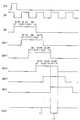
도 4는 도 1의 표시 패널(100)의 구동 신호들의 파형을 나타내는 타이밍도이다.4 is a timing chart showing waveforms of driving signals of the
도 1 내지 도 4를 참조하면, 수직 개시 신호(STV)가 온(ON)이 되면 상기 표시 패널(100)의 상기 제1 게이트 라인(G1)에 제1 게이트 신호가 인가되기 시작하여, 제N 게이트 라인에 제N 게이트 신호(GN)가 인가되고, 마지막 게이트 라인까지 순차적으로 게이트 신호들이 인가된다.1 to 4, when the vertical start signal STV is turned on, the first gate signal is applied to the first gate line G1 of the
본 실시예에서, 상기 게이트 신호들은 3 수평 주기(3H)동안 온(ON)이 되어 제1 및 제2 수평 주기 동안 프리차지가 수행되고, 제3 수평 주기에 화소의 계조 데이터가 충전된다.In the present embodiment, the gate signals are turned ON for 3
예를 들어, 상기 제N 게이트 신호(GN)는 제N-2, 제N-1, 제N 수평 주기(N-2H, N-1H, NH)동안 온이 된다. 상기 제N-2 수평 주기에는 제N-2 게이트 라인에 대응하는 데이터 전압(DN)이 상기 제N 게이트 라인에 연결된 화소에 프리차지 된다. 상기 제N-1 수평 주기에는 제N-1 게이트 라인에 대응하는 데이터 전압(DN)이 상기 제N 게이트 라인에 연결된 화소에 프리차지 된다. 상기 제N 수평 주기에는 제N 게이트 라인에 대응하는 데이터 전압(DN)이 상기 제N 게이트 라인에 충전된다.For example, the N-th gate signal GN is turned on during N-2, N-1, and N-th horizontal periods N-2H, N-1H, and NH. In the (N-2) th horizontal period, the data voltage DN corresponding to the (N-2) th gate line is precharged to the pixel connected to the Nth gate line. In the (N-1) th horizontal period, the data voltage DN corresponding to the (N-1) th gate line is precharged to the pixel connected to the Nth gate line. In the Nth horizontal period, the data voltage DN corresponding to the Nth gate line is charged in the Nth gate line.
예를 들어, 상기 제N+1 게이트 신호(GN+1)는 제N-1, 제N, 제N+1 수평 주기(N-1H, NH, N+1H)동안 온이 된다. 상기 제N-1 수평 주기에는 제N-1 게이트 라인에 대응하는 데이터 전압(DN)이 상기 제N+1 게이트 라인에 연결된 화소에 프리차지 된다. 상기 제N 수평 주기에는 제N 게이트 라인에 대응하는 데이터 전압(DN)이 상기 제N+1 게이트 라인에 연결된 화소에 프리차지 된다. 상기 제N 수평 주기에는 제N+1 게이트 라인에 대응하는 데이터 전압(DN)이 상기 제N+1 게이트 라인에 충전된다.For example, the (N + 1) th gate signal GN + 1 is turned on during the (N-1) th, Nth, and N + 1th horizontal periods N-1H, NH, and N + 1H. In the (N-1) th horizontal period, a data voltage DN corresponding to the (N-1) th gate line is precharged to a pixel connected to the (N + 1) th gate line. In the Nth horizontal period, a data voltage DN corresponding to the Nth gate line is precharged to a pixel connected to the (N + 1) th gate line. And the data voltage DN corresponding to the (N + 1) -th gate line is charged in the (N + 1) -th gate line in the N-th horizontal period.
상기 제N-1 수평 주기(N-1H)에 대응하는 데이터 전압(DN)은 고 계조를 나타내고 상기 제N 수평 주기(NH)에 대응하는 데이터 전압(DN)은 저 계조를 나타내므로, 상기 제N 게이트 라인(GN)에 연결된 화소에서 표시 오류가 발생할 수 있다.The data voltage DN corresponding to the (N-1) th horizontal period (N-1H) represents a high gray scale level and the data voltage DN corresponding to the (N) A display error may occur in a pixel connected to the N gate line GN.
상기 제N 게이트 라인(GN)에 연결된 화소에서 표시 오류가 발생하면, 상기 계조 데이터 보정부(220)는 상기 표시 오류가 발생한 데이터 라인을 제외한 다른 데이터 라인에 대응하는 입력 계조 데이터(DATA)를 증가시켜 보정 계조 데이터(CDATA)를 생성한다.When a display error occurs in a pixel connected to the Nth gate line GN, the gradation
이에 따라, 상기 데이터 구동부(500)는 상기 보정 계조 데이터(CDATA)를 기초로 상기 제N 게이트 라인(GN)에 연결된 화소들에 입력 계조 데이터(DATA)가 나타내는 계조보다 높은 데이터 전압을 출력한다.Accordingly, the
상기 스토리지 전압(VCST)은 제N-2 내지 제N+2 수평 주기(N-2H 내지 N+2H)에서 제1 레벨(L1)을 가지나, 상기 제N+3 수평 주기(N+3H)에서 상기 제1 레벨(L1)보다 낮은 제2 레벨(L2)을 갖는다.The storage voltage VCST has a first level L1 in the (N + 2) th to (N + 2) th horizontal periods (N + 2H to N + 2H) And a second level (L2) lower than the first level (L1).
도 2를 참조하면, 상기 제N+3 게이트 라인은 상기 제N 게이트 라인에 연결된 화소들에 스토리지 전압(VCST)을 인가하는 상기 스토리지 스위치들의 제어 전극에 연결된다.Referring to FIG. 2, the (N + 3) -th gate line is connected to a control electrode of the storage switches for applying a storage voltage VCST to pixels connected to the N-th gate line.
따라서, 상기 제N+3 수평 주기(N+3H)에서 상기 제1 레벨(L1)보다 낮은 상기 제2 레벨(L2)을 갖는 상기 스토리지 전압(VCST)이 상기 제N 게이트 라인에 연결된 화소들에 충전된 데이터 전압을 감소시킨다.Therefore, the storage voltage VCST having the second level L2 lower than the first level L1 in the (N + 3) -th horizontal period N + 3H is applied to the pixels connected to the Thereby reducing the charged data voltage.
그러므로, 상기 계조 데이터 보정부(220)의 동작에 의해 원하는 계조보다 높은 값을 표시하도록 보정된 상기 제N 게이트 라인에 연결된 화소들의 데이터 전압은 원하는 계조를 표시할 수 있다. 따라서, 상기 표시 패널(100) 상의 표시 오류를 제거할 수 있다.Therefore, the data voltage of the pixels coupled to the Nth gate line, which is corrected to display a value higher than a desired gray level by the operation of the gray level
상기 스토리지 전압(VCST)이 제2 레벨(L2)을 갖는 시점은 제N+3 수평 주기(N+3H)로 제한되지 않는다. 상기 스토리지 전압(VCST)은 제N+K 수평 주기에서 상기 제2 레벨을 갖도록 변경될 수 있다. 여기서, K는 자연수이다. 단, 상기 제2 레벨(L2)을 갖는 타이밍에 따라 상기 스토리지 스위치의 제어 전극과 연결되는 상기 게이트 라인도 변경되어야 한다.The time when the storage voltage VCST has the second level L2 is not limited to the (N + 3) -th horizontal period N + 3H. The storage voltage VCST may be changed to have the second level in the (N + K) horizontal period. Here, K is a natural number. However, the gate line connected to the control electrode of the storage switch must be changed according to the timing with the second level (L2).
상기 스토리지 전압(VCST)은 상기 제N+2 수평 주기(N+2H)에 상기 제2 레벨(L2)을 갖도록 변경될 수 있다.The storage voltage VCST may be changed to have the second level L2 in the (N + 2) -th horizontal period (N + 2H).
예를 들어, 상기 스토리지 전압(VCST)이 제N+2 수평 주기(N+2H)에서 상기 제2 레벨(L2)을 갖는 경우, 상기 제N 게이트 라인에 연결된 화소들에 스토리지 전압(VCST)을 전달하는 스토리지 스위치의 제어 전극은 제N+2 게이트 라인과 연결되어야 한다.For example, when the storage voltage VCST has the second level L2 in the (N + 2) -th horizontal period (N + 2H), the storage voltage VCST is applied to the pixels connected to the The control electrode of the storage switch to be transferred must be connected to the (N + 2) -th gate line.
예를 들어, 상기 스토리지 전압(VCST)이 제N+4 수평 주기(N+4H)에서 상기 제2 레벨(L2)을 갖는 경우, 상기 제N 게이트 라인에 연결된 화소들에 스토리지 전압(VCST)을 전달하는 스토리지 스위치의 제어 전극은 제N+4 게이트 라인과 연결되어야 한다.For example, when the storage voltage VCST has the second level L2 in the (N + 4) -th horizontal period (N + 4H), the storage voltage VCST is applied to the pixels connected to the The control electrode of the storage switch to be transferred must be connected to the (N + 4) th gate line.
바람직하게는 K는 3이상일 수 있다. 상기 제N 게이트 라인에 인가되는 상기 제N 게이트 신호(GN)가 오프(OFF)된 후인 상기 제N+3 수평 주기 이후에 상기 제2 레벨(L2)을 갖는 경우, 상기 표시 패널이 더욱 안정되게 구동될 수 있다.Preferably, K may be 3 or more. When the display panel has the second level (L2) after the (N + 3) th horizontal period after the Nth gate signal GN applied to the Nth gate line is turned off, Can be driven.
상기 스토리지 전압(VCST)의 감소에 따라 상기 충전된 데이터 전압이 감소되는 정도는 아래의 수식 1과 같다.The degree to which the charged data voltage is reduced as the storage voltage VCST decreases is expressed by
[수식 1][Equation 1]

여기서, ΔVCST는 스토리지 전압의 감소량이고, CLC는 상기 액정 캐패시터의 캐패시턴스, CST는 상기 스토리지 캐패시터의 캐패시턴스, ΔVCLC는 상기 충전된 데이터 전압의 감소량이다.Where CLC is the capacitance of the liquid crystal capacitor, CST is the capacitance of the storage capacitor, and DELTA VCLC is the amount of decrease of the charged data voltage.
예를 들어, 상기 계조 데이터 보정부(220)에 의해, 상기 데이터 전압이 2V 증가한 경우, 상기 스토리지 전압(VCST)을 조절하여 상기 데이터 전압을 다시 2V 감소시켜야 한다.For example, when the data voltage is increased by 2V, the gray scale
ΔVCLC=2이고, CLC:CST = 2:1인 경우, 이다. 즉, 상기 스토리지 전압(VCST)을 6V 감소시키면, 상기 액정 캐패시터(CLC)에 충전된 데이터 전압(VCLC)을 원하는 계조로 회복시켜 상기 표시 오류를 제거할 수 있다. 이때, 상기 스토리지 전압(VCST)의 제2 레벨(L2)은 상기 제1 레벨(L1)보다 6V 낮게 설정한다.And? CLC = 2, and CLC: CST = 2: 1. That is, if the storage voltage VCST is reduced by 6V, the data voltage VCLC charged in the liquid crystal capacitor CLC can be restored to a desired gray level to eliminate the display error. At this time, the second level L2 of the storage voltage VCST is set 6V lower than the first level L1.
본 실시예에 따르면, 상기 에러 검출부(210)는 표시 오류를 검출하고, 상기 계조 데이터 보정부(220)는 입력 계조 데이터(DATA)를 보정한다. 또한, 상기 스토리지 전압 생성부(300)는 상기 스토리지 전압(VCST)의 레벨을 조절하여 상기 표시 패널(100)의 표시 에러를 방지할 수 있다.According to the present embodiment, the
도 5는 본 발명의 다른 실시예에 따른 표시 패널의 화소 구조를 나타내는 평면도이다.5 is a plan view showing a pixel structure of a display panel according to another embodiment of the present invention.
본 실시예에 따른 표시 장치는 상기 제N 게이트 라인에 연결된 화소에 스토리지 전압(VCST)을 인가하는 스토리지 스위치의 제어 전극이 제N+2 게이트 라인에 연결되는 것을 제외하면, 도 1 내지 도 4에 따른 표시 장치와 동일하므로, 동일하거나 대응되는 구성 요소에 대해서는 동일한 참조번호를 이용하고, 중복되는 설명은 생략한다.1 to 4 except that the control electrode of the storage switch for applying the storage voltage VCST to the pixel connected to the Nth gate line is connected to the (N + 2) -th gate line. The same reference numerals are used for the same or corresponding constituent elements, and redundant explanations are omitted.
본 실시예에 따른 표시 패널의 구동 방법은 상기 게이트 신호가 2 수평 주기(2H) 동안 온(ON)이 되어 1 수평 주기(1H) 동안 프리차지를 수행하는 것을 제외하면, 도 1 내지 도 4에 따른 표시 패널의 구동 방법과 동일하므로, 동일하거나 대응되는 구성 요소에 대해서는 동일한 참조번호를 이용하고, 중복되는 설명은 생략한다.1 to 4, except that the gate signal is turned on for two horizontal periods (2H) and precharging is performed for one horizontal period (1H). The same reference numerals are used for the same or corresponding constituent elements, and redundant explanations are omitted.
도 1 및 도 5를 참조하면, 상기 표시 패널(100)은 복수의 화소들(P11, P12, P13, P14, P15, P21, P22, P23, P24, P25)을 포함한다.Referring to FIGS. 1 and 5, the
상기 화소들(P11 내지 P25)은 제1 화소 열 및 제2 화소 열 내에 배치된다. 상기 제1 화소 열은 제1 내지 제5 화소들(P11, P12, P13, P14, P15)을 포함한다. 상기 제2 화소 열은 제6 내지 제10 화소들(P21, P22, P23, P24, P25)을 포함한다.The pixels P11 to P25 are arranged in the first pixel column and the second pixel column. The first column includes the first through fifth pixels P11, P12, P13, P14 and P15. And the second pixel column includes the sixth to tenth pixels P21, P22, P23, P24, and P25.
각 화소들은 상기 게이트 라인(GL) 및 데이터 라인(DL)에 전기적으로 연결된다. 이때, 상기 데이터 라인(DL)은 인접하는 화소 열 내의 화소들에 교대로 연결된다.Each pixel is electrically connected to the gate line GL and the data line DL. At this time, the data lines DL are alternately connected to the pixels in the adjacent pixel columns.
각 화소들은 상기 스위칭 소자(TFT), 상기 액정 캐패시터(CLC) 및 상기 스토리지 캐패시터(CST)를 포함한다.Each pixel includes the switching element (TFT), the liquid crystal capacitor (CLC), and the storage capacitor (CST).
복수의 스토리지 스위치들(SW11, SW12, SW13, SW14, SW21, SW22, SW23, SW24, SW31, SW32, SW33, SW34, SW41, SW42, SW43, SW44)은 상기 표시 패널(100)에 스토리지 전압(VCST)을 인가한다.A plurality of storage switches SW11, SW12, SW13, SW14, SW21, SW22, SW23, SW24, SW31, SW32, SW33, SW34, SW41, SW42, SW43, SW44 are connected to the
정상, 제1 및 제2 스토리지 전압들(VCST0, VCSTP, VCSTN)은 제3 게이트 라인(GL3)과 연결되는 제1 내지 제4 스토리지 스위치들(SW11 내지 SW14)을 통해 상기 제1 게이트 라인(GL1)에 연결되는 상기 제1 및 제6 화소들(P11, P21)에 인가된다.The first and second storage voltages VCST0, VCSTP and VCSTN are connected to the first gate line GL1 through the first to fourth storage switches SW11 to SW14 connected to the third gate line GL3, The first and sixth pixels P11 and P21 are connected to the first and sixth pixels P11 and P21.
상기 정상, 제1 및 제2 스토리지 전압들(VCST0, VCSTP, VCSTN)은 제4 게이트 라인(GL4)과 연결되는 제5 내지 제8 스토리지 스위치들(SW21 내지 SW24)을 통해 상기 제2 게이트 라인(GL2)에 연결되는 상기 제2 및 제7 화소들(P12, P22)에 인가된다.The normal, first and second storage voltages VCST0, VCSTP and VCSTN are connected to the second gate line GL2 through fifth to eighth storage switches SW21 to SW24 connected to the fourth gate line GL4. And the second and seventh pixels P12 and P22 connected to the first and second pixels GL1 and GL2.
상기 정상, 제1 및 제2 스토리지 전압들(VCST0, VCSTP, VCSTN)은 제5 게이트 라인(GL5)과 연결되는 제9 내지 제12 스토리지 스위치들(SW31 내지 SW34)을 통해 상기 제3 게이트 라인(GL3)에 연결되는 상기 제3 및 제8 화소들(P13, P23)에 인가된다.The normal, first and second storage voltages VCST0, VCSTP and VCSTN are applied to the third gate line GL2 through the ninth through twelfth storage switches SW31 through SW34 connected to the fifth gate line GL5. And the third and eighth pixels P13 and P23 connected to the third and fourth pixels GL3 and GL3.
일반화하여 표현하면, 상기 정상, 제1 및 제2 스토리지 전압들(VCST0, VCSTP, VCSTN)은 상기 제N+2 게이트 라인과 연결되는 상기 스토리지 스위치들을 통해 상기 제N 게이트 라인에 연결되는 화소들에 인가된다. 여기서, N은 자연수이다.In general terms, the normal, first and second storage voltages VCST0, VCSTP, VCSTN are connected to the pixels connected to the Nth gate line through the storage switches connected to the (N + 2) . Here, N is a natural number.
도 6은 도 5의 표시 패널의 구동 신호들의 파형을 나타내는 타이밍도이다.6 is a timing chart showing waveforms of driving signals of the display panel of Fig.
도 1, 도 3, 도 5 및 도 6을 참조하면, 수직 개시 신호(STV)가 온(ON)이 되면 상기 표시 패널(100)의 상기 제1 게이트 라인(G1)에 제1 게이트 신호가 인가되기 시작하여, 제N 게이트 라인에 제N 게이트 신호(GN)가 인가되고, 마지막 게이트 라인까지 순차적으로 게이트 신호들이 인가된다.Referring to FIGS. 1, 3, 5 and 6, when the vertical start signal STV is turned on, a first gate signal is applied to the first gate line G1 of the
본 실시예에서, 상기 게이트 신호들은 2 수평 주기(2H)동안 온(ON)이 되어 제1 수평 주기 동안 프리차지가 수행되고, 제2 수평 주기에 화소의 계조 데이터가 충전된다.In the present embodiment, the gate signals are turned on for two horizontal periods (2H), precharging is performed during the first horizontal period, and gray scale data of the pixels are charged in the second horizontal period.
예를 들어, 상기 제N 게이트 신호(GN)는 제N-1, 제N 수평 주기(N-1H, NH)동안 온이 된다. 상기 제N-1 수평 주기에는 제N-1 게이트 라인에 대응하는 데이터 전압(DN)이 상기 제N 게이트 라인에 연결된 화소에 프리차지 된다. 상기 제N 수평 주기에는 제N 게이트 라인에 대응하는 데이터 전압(DN)이 상기 제N 게이트 라인에 충전된다.For example, the Nth gate signal GN is turned on during the (N-1) th and Nth horizontal periods (N-1H, NH). In the (N-1) th horizontal period, the data voltage DN corresponding to the (N-1) th gate line is precharged to the pixel connected to the Nth gate line. In the Nth horizontal period, the data voltage DN corresponding to the Nth gate line is charged in the Nth gate line.
예를 들어, 상기 제N+1 게이트 신호(GN+1)는 제N, 제N+1 수평 주기(NH, N+1H)동안 온이 된다. 상기 제N 수평 주기에는 제N 게이트 라인에 대응하는 데이터 전압(DN)이 상기 제N+1 게이트 라인에 연결된 화소에 프리차지 된다. 상기 제N 수평 주기에는 제N+1 게이트 라인에 대응하는 데이터 전압(DN)이 상기 제N+1 게이트 라인에 충전된다.For example, the (N + 1) th gate signal GN + 1 is turned on during the (N + 1) th horizontal period (NH, N + 1H). In the Nth horizontal period, a data voltage DN corresponding to the Nth gate line is precharged to a pixel connected to the (N + 1) th gate line. And the data voltage DN corresponding to the (N + 1) -th gate line is charged in the (N + 1) -th gate line in the N-th horizontal period.
상기 제N-1 수평 주기(N-1H)에 대응하는 데이터 전압(DN)은 고 계조를 나타내고 상기 제N 수평 주기(NH)에 대응하는 데이터 전압(DN)은 저 계조를 나타내므로, 상기 제N 게이트 라인(GN)에 연결된 화소에서 표시 오류가 발생할 수 있다.The data voltage DN corresponding to the (N-1) th horizontal period (N-1H) represents a high gray scale level and the data voltage DN corresponding to the (N) A display error may occur in a pixel connected to the N gate line GN.
상기 제N 게이트 라인(GN)에 연결된 화소에서 표시 오류가 발생하면, 상기 계조 데이터 보정부(220)는 상기 표시 오류가 발생한 데이터 라인을 제외한 다른 데이터 라인에 대응하는 입력 계조 데이터(DATA)를 증가시켜 보정 계조 데이터(CDATA)를 생성한다.When a display error occurs in a pixel connected to the Nth gate line GN, the gradation
이에 따라, 상기 데이터 구동부(500)는 상기 보정 계조 데이터(CDATA)를 기초로 상기 제N 게이트 라인(GN)에 연결된 화소들에 입력 계조 데이터(DATA)가 나타내는 계조보다 높은 데이터 전압을 출력한다.Accordingly, the
상기 스토리지 전압(VCST)은 제N-1 내지 제N+1 수평 주기(N-1H 내지 N+1H)에서 제1 레벨(L1)을 가지나, 상기 제N+2 수평 주기(N+2H)에서 상기 제1 레벨(L1)보다 낮은 제2 레벨(L2)을 갖는다.The storage voltage VCST has a first level L1 in the (N-1) th to (N + 1) th horizontal periods (N + 1H to N + 1H) And a second level (L2) lower than the first level (L1).
도 5를 참조하면, 상기 제N+2 게이트 라인은 상기 제N 게이트 라인에 연결된 화소들에 스토리지 전압(VCST)을 인가하는 상기 스토리지 스위치들의 제어 전극에 연결된다.Referring to FIG. 5, the (N + 2) -th gate line is connected to a control electrode of the storage switches for applying a storage voltage VCST to pixels connected to the N-th gate line.
따라서, 상기 제N+2 수평 주기(N+2H)에서 상기 제1 레벨(L1)보다 낮은 상기 제2 레벨(L2)을 갖는 상기 스토리지 전압(VCST)이 상기 제N 게이트 라인에 연결된 화소들에 충전된 데이터 전압을 감소시킨다.Therefore, the storage voltage VCST having the second level L2 lower than the first level L1 in the (N + 2) -th horizontal period N + 2H is applied to the pixels connected to the Thereby reducing the charged data voltage.
그러므로, 상기 계조 데이터 보정부(220)의 동작에 의해 원하는 계조보다 높은 값을 표시하도록 보정된 상기 제N 게이트 라인에 연결된 화소들의 데이터 전압은 원하는 계조를 표시할 수 있다. 따라서, 상기 표시 패널(100) 상의 표시 오류를 제거할 수 있다.Therefore, the data voltage of the pixels coupled to the Nth gate line, which is corrected to display a value higher than a desired gray level by the operation of the gray level
상기 스토리지 전압(VCST)이 제2 레벨(L2)을 갖는 시점은 제N+2 수평 주기(N+2H)로 제한되지 않는다. 상기 스토리지 전압(VCST)은 제N+K 수평 주기에서 상기 제2 레벨을 갖도록 변경될 수 있다. 여기서, K는 자연수이다. 단, 상기 제2 레벨(L2)을 갖는 타이밍에 따라 상기 스토리지 스위치의 제어 전극과 연결되는 상기 게이트 라인도 변경되어야 한다.The time when the storage voltage VCST has the second level L2 is not limited to the (N + 2) -th horizontal period (N + 2H). The storage voltage VCST may be changed to have the second level in the (N + K) horizontal period. Here, K is a natural number. However, the gate line connected to the control electrode of the storage switch must be changed according to the timing with the second level (L2).
바람직하게는 K는 2이상일 수 있다. 상기 제N 게이트 라인에 인가되는 상기 제N 게이트 신호(GN)가 오프(OFF)된 후인 상기 제N+2 수평 주기 이후에 상기 제2 레벨(L2)을 갖는 경우, 상기 표시 패널이 더욱 안정되게 구동될 수 있다.Preferably, K may be two or more. When the display panel has the second level (L2) after the (N + 2) th horizontal period after the Nth gate signal GN applied to the Nth gate line is turned off, Can be driven.
본 실시예에 따르면, 상기 에러 검출부(210)는 표시 오류를 검출하고, 상기 계조 데이터 보정부(220)는 입력 계조 데이터(DATA)를 보정한다. 또한, 상기 스토리지 전압 생성부(300)는 상기 스토리지 전압(VCST)의 레벨을 조절하여 상기 표시 패널(100)의 표시 에러를 방지할 수 있다.According to the present embodiment, the
이상에서 설명한 바와 같이, 본 발명의 실시예들에 따르면, 계조 데이터를 보정하고 스토리지 전압을 조절하여 표시 에러를 방지할 수 있다. 따라서, 표시 패널의 표시 품질을 향상시킬 수 있다.As described above, according to the embodiments of the present invention, display error can be prevented by correcting the gray level data and adjusting the storage voltage. Therefore, the display quality of the display panel can be improved.
이상에서는 본 발명의 바람직한 실시예들을 참조하여 설명하였지만, 해당 기술분야의 숙련된 당업자 또는 해당 기술분야에 통상의 지식을 갖는 자라면 후술될 특허청구범위에 기재된 본 발명의 사상 및 기술 영역으로부터 벗어나지 않는 범위 내에서 본 발명을 다양하게 수정 및 변경시킬 수 있음을 이해할 수 있을 것이다.While the present invention has been described with reference to exemplary embodiments, it is to be understood that the invention is not limited to the disclosed exemplary embodiments, but, on the contrary, is intended to cover various modifications and equivalent arrangements included within the spirit and scope of the appended claims. It will be understood that various modifications and changes may be made thereto without departing from the scope of the present invention.
100: 표시 패널200: 타이밍 제어부
210: 에러 검출부220: 계조 데이터 보정부
230: 신호 생성부300: 스토리지 전압 생성부
400: 게이트 구동부500: 데이터 구동부100: display panel 200: timing controller
210: error detection unit 220: gradation data correction unit
230: Signal generator 300: Storage voltage generator
400: Gate driver 500: Data driver
Claims (20)
Translated fromKorean상기 보정 계조 데이터를 기초로 데이터 전압을 생성하여 화소 전극, 스토리지 전극, 게이트 라인 및 제1 화소 열의 상기 화소 전극과 제2 화소 열의 상기 화소 전극에 교대로 연결되는 데이터 라인을 포함하는 표시 패널에 출력하는 단계;
제1 레벨 및 상기 제1 레벨보다 낮은 제2 레벨을 갖는 스토리지 전압을 생성하는 단계; 및
상기 스토리지 전압을 상기 표시 패널에 인가하는 단계를 포함하고,
상기 데이터 전압은 상기 데이터 라인을 통해 상기 화소 전극에 인가되고, 상기 스토리지 전압은 상기 스토리지 전극에 인가되며,
상기 계조 데이터를 기초로 표시 에러를 검출하는 단계를 더 포함하고,
상기 보정 계조 데이터를 생성하는 단계는 상기 표시 에러가 검출되면 상기 계조 데이터를 증가시키며,
상기 보정 계조 데이터를 생성하는 단계는
제M 데이터 라인의 상기 계조 데이터에서 상기 표시 에러가 검출되면 상기 제M 데이터 라인을 제외한 데이터 라인들의 상기 계조 데이터들을 증가시키는 것을 특징으로 하는 표시 패널의 구동 방법(M은 자연수).A step of generating correction grayscale data by increasing grayscale data corresponding to the Nth gate line (N is a natural number);
Generating a data voltage based on the correction gradation data and outputting it to a display panel including a pixel electrode, a storage electrode, a gate line, and a data line alternately connected to the pixel electrode of the first pixel train and the pixel electrode of the second pixel train; ;
Generating a storage voltage having a first level and a second level lower than the first level; And
And applying the storage voltage to the display panel,
The data voltage is applied to the pixel electrode through the data line, the storage voltage is applied to the storage electrode,
Further comprising the step of detecting a display error based on the grayscale data,
Wherein the step of generating the correction gradation data increases the gradation data if the display error is detected,
The step of generating the correction tone data
(M is a natural number) when the display error is detected in the grayscale data of the Mth data line, wherein the grayscale data of the data lines excluding the Mth data line is increased.
제N-1 게이트 라인에 대응하는 이전 계조 데이터를 상기 제N 게이트 라인에 대응하는 현재 계조 데이터와 비교하는 것을 특징으로 하는 표시 패널의 구동 방법.2. The method of claim 1, wherein detecting the display error comprises:
And comparing the previous gradation data corresponding to the (N-1) th gate line with the current gradation data corresponding to the Nth gate line.
상기 이전 계조 데이터가 상기 현재 계조 데이터보다 큰 계조를 가질 때 상기 표시 에러를 검출하는 것을 특징으로 하는 표시 패널의 구동 방법.5. The method of claim 4, wherein detecting the display error comprises:
And the display error is detected when the previous gradation data has a gradation larger than the current gradation data.
상기 보정 계조 데이터를 기초로 데이터 전압을 생성하여 화소 전극, 스토리지 전극, 게이트 라인 및 제1 화소 열의 상기 화소 전극과 제2 화소 열의 상기 화소 전극에 교대로 연결되는 데이터 라인을 포함하는 표시 패널에 출력하는 단계;
제1 레벨 및 상기 제1 레벨보다 낮은 제2 레벨을 갖는 스토리지 전압을 생성하는 단계; 및
상기 스토리지 전압을 상기 표시 패널에 인가하는 단계를 포함하고,
상기 데이터 전압은 상기 데이터 라인을 통해 상기 화소 전극에 인가되고, 상기 스토리지 전압은 상기 스토리지 전극에 인가되며,
상기 스토리지 전압을 인가하는 단계는
제N+K 게이트 신호에 의해 제어되고,
상기 K는 2이상의 자연수인 것을 특징으로 하는 표시 패널의 구동 방법.A step of generating correction grayscale data by increasing grayscale data corresponding to the Nth gate line (N is a natural number);
Generating a data voltage based on the correction gradation data and outputting it to a display panel including a pixel electrode, a storage electrode, a gate line, and a data line alternately connected to the pixel electrode of the first pixel train and the pixel electrode of the second pixel train; ;
Generating a storage voltage having a first level and a second level lower than the first level; And
And applying the storage voltage to the display panel,
The data voltage is applied to the pixel electrode through the data line, the storage voltage is applied to the storage electrode,
The step of applying the storage voltage
An N + K gate signal,
Wherein K is a natural number of 2 or more.
제N+K 수평 주기에서 상기 제2 레벨을 갖는 것을 특징으로 하는 표시 패널의 구동 방법.7. The method of claim 6, wherein the storage voltage
And the second level in the (N + K) horizontal period.
상기 화소 전극은 상기 제N-2 및 제N-1 수평 주기 동안 프리차지 되며,
상기 K는 3이상인 것을 특징으로 하는 표시 패널의 구동 방법.The method of claim 7, wherein the gate signal applied to the Nth gate line is continuously turned on during N-2, N-1, and Nth horizontal periods,
The pixel electrode is precharged during the (N-2) th and (N-1) -th horizontal periods,
Wherein K is 3 or more.
상기 화소 전극은 상기 제N-1 수평 주기 동안 프리차지 되며,
상기 K는 2이상인 것을 특징으로 하는 표시 패널의 구동 방법.8. The method of claim 7, wherein the gate signal applied to the Nth gate line is continuously turned on during N-1th and Nth horizontal periods,
The pixel electrode is precharged during the (N-1) -th horizontal period,
And K is two or more.
상기 화소의 장변은 상기 게이트 라인과 평행한 것을 특징으로 하는 표시 패널의 구동 방법.2. The liquid crystal display device according to claim 1, wherein a pixel defined as a region where the gate line and the data line meet is a rectangular shape,
And the long side of the pixel is parallel to the gate line.
제N 게이트 라인에 대응하는 계조 데이터를 증가시켜 보정 계조 데이터를 생성하는 계조 데이터 보정부(N은 자연수);
상기 보정 계조 데이터를 기초로 데이터 전압을 생성하여 상기 표시 패널에 출력하는 데이터 구동부; 및
제1 레벨 및 상기 제1 레벨보다 낮은 제2 레벨을 갖는 스토리지 전압을 생성하여 상기 표시 패널에 인가하는 스토리지 전압 생성부를 포함하고,
상기 데이터 전압은 상기 데이터 라인을 통해 상기 화소 전극에 인가되고, 상기 스토리지 전압은 상기 스토리지 전극에 인가되며,
상기 계조 데이터를 기초로 표시 에러를 검출하는 에러 검출부를 더 포함하고,
상기 계조 데이터 보정부는
제M 데이터 라인의 상기 계조 데이터에서 상기 표시 에러가 검출되면 상기 제M 데이터 라인을 제외한 데이터 라인들의 상기 계조 데이터들을 증가시키는 것을 특징으로 하는 표시 장치(M은 자연수).A display panel including a pixel electrode, a storage electrode, a gate line, and a data line alternately connected to the pixel electrode of the first pixel column and the pixel electrode of the second pixel column;
A gradation data correcting section (N is a natural number) for generating correction gradation data by increasing the gradation data corresponding to the Nth gate line;
A data driver for generating a data voltage based on the correction gradation data and outputting the data voltage to the display panel; And
And a storage voltage generator for generating a storage voltage having a first level and a second level lower than the first level and applying the generated storage voltage to the display panel,
The data voltage is applied to the pixel electrode through the data line, the storage voltage is applied to the storage electrode,
Further comprising an error detecting section for detecting a display error on the basis of the grayscale data,
The tone data correction unit
(M is a natural number) when the display error is detected in the grayscale data of the Mth data line, and increases the grayscale data of the data lines excluding the Mth data line.
제N-1 게이트 라인에 대응하는 이전 계조 데이터를 상기 제N 게이트 라인에 대응하는 현재 계조 데이터와 비교하여 상기 표시 에러를 검출하는 것을 특징으로 하는 표시 장치.12. The apparatus of claim 11, wherein the error detector
And the display error is detected by comparing the previous gradation data corresponding to the (N-1) th gate line with the current gradation data corresponding to the Nth gate line.
상기 이전 계조 데이터가 상기 현재 계조 데이터보다 큰 계조를 가질 때 상기 표시 에러를 검출하는 것을 특징으로 하는 표시 장치.15. The apparatus of claim 14, wherein the error detector
And detects the display error when the previous gradation data has a higher gradation than the current gradation data.
제N 게이트 라인에 대응하는 계조 데이터를 증가시켜 보정 계조 데이터를 생성하는 계조 데이터 보정부(N은 자연수);
상기 보정 계조 데이터를 기초로 데이터 전압을 생성하여 상기 표시 패널에 출력하는 데이터 구동부; 및
제1 레벨 및 상기 제1 레벨보다 낮은 제2 레벨을 갖는 스토리지 전압을 생성하여 상기 표시 패널에 인가하는 스토리지 전압 생성부를 포함하고,
상기 데이터 전압은 상기 데이터 라인을 통해 상기 화소 전극에 인가되고, 상기 스토리지 전압은 상기 스토리지 전극에 인가되며,
상기 스토리지 전압을 상기 표시 패널의 상기 스토리지 전극에 인가하는 스토리지 스위치를 더 포함하고,
상기 스토리지 스위치의 제어 전극은 제N+K 게이트 라인과 연결되며,
상기 K는 2이상의 자연수인 것을 특징으로 하는 표시 장치.A display panel including a pixel electrode, a storage electrode, a gate line, and a data line alternately connected to the pixel electrode of the first pixel column and the pixel electrode of the second pixel column;
A gradation data correcting section (N is a natural number) for generating correction gradation data by increasing the gradation data corresponding to the Nth gate line;
A data driver for generating a data voltage based on the correction gradation data and outputting the data voltage to the display panel; And
And a storage voltage generator for generating a storage voltage having a first level and a second level lower than the first level and applying the generated storage voltage to the display panel,
The data voltage is applied to the pixel electrode through the data line, the storage voltage is applied to the storage electrode,
Further comprising a storage switch for applying the storage voltage to the storage electrode of the display panel,
The control electrode of the storage switch is connected to the (N + K) -th gate line,
And K is a natural number of 2 or more.
제N+K 수평 주기에서 상기 제2 레벨을 갖는 것을 특징으로 하는 표시 장치.17. The method of claim 16,
And has the second level in an (N + K) horizontal period.
상기 화소 전극은 상기 제N-2 및 제N-1 수평 주기 동안 프리차지 되며,
상기 K는 3이상인 것을 특징으로 하는 표시 장치.The method of claim 17, wherein the gate signal applied to the Nth gate line is continuously turned on during N-2, N-1, and Nth horizontal periods,
The pixel electrode is precharged during the (N-2) th and (N-1) -th horizontal periods,
And K is 3 or more.
상기 화소 전극은 상기 제N-1 수평 주기 동안 프리차지 되며,
상기 K는 2이상인 것을 특징으로 하는 표시 장치.18. The method of claim 17, wherein the gate signal applied to the Nth gate line is continuously turned on during N-1th and Nth horizontal periods,
The pixel electrode is precharged during the (N-1) -th horizontal period,
And K is two or more.
상기 화소의 장변은 상기 게이트 라인과 평행한 것을 특징으로 하는 표시 장치.The liquid crystal display device according to claim 11, wherein the pixel defined as the region where the gate line and the data line meet is rectangular,
And a long side of the pixel is parallel to the gate line.
Priority Applications (2)
| Application Number | Priority Date | Filing Date | Title |
|---|---|---|---|
| KR1020110017890AKR101874106B1 (en) | 2011-02-28 | 2011-02-28 | Method of driving display panel and display apparatus for performing the same |
| US13/241,373US9478184B2 (en) | 2011-02-28 | 2011-09-23 | Method of driving display panel and display apparatus for performing the same |
Applications Claiming Priority (1)
| Application Number | Priority Date | Filing Date | Title |
|---|---|---|---|
| KR1020110017890AKR101874106B1 (en) | 2011-02-28 | 2011-02-28 | Method of driving display panel and display apparatus for performing the same |
Publications (2)
| Publication Number | Publication Date |
|---|---|
| KR20120098139A KR20120098139A (en) | 2012-09-05 |
| KR101874106B1true KR101874106B1 (en) | 2018-07-04 |
Family
ID=46718709
Family Applications (1)
| Application Number | Title | Priority Date | Filing Date |
|---|---|---|---|
| KR1020110017890AExpired - Fee RelatedKR101874106B1 (en) | 2011-02-28 | 2011-02-28 | Method of driving display panel and display apparatus for performing the same |
Country Status (2)
| Country | Link |
|---|---|
| US (1) | US9478184B2 (en) |
| KR (1) | KR101874106B1 (en) |
Families Citing this family (7)
| Publication number | Priority date | Publication date | Assignee | Title |
|---|---|---|---|---|
| KR101773419B1 (en)* | 2010-11-22 | 2017-09-01 | 삼성디스플레이 주식회사 | Methode for compensating data and display apparatus performing the method |
| KR102127902B1 (en)* | 2013-10-14 | 2020-06-30 | 삼성디스플레이 주식회사 | Display device and methods of driving display device |
| KR102154186B1 (en)* | 2013-12-03 | 2020-09-10 | 삼성전자 주식회사 | Timing Controller, Source Driver, Display Driving Circuit improving test efficiency and Operating Method thereof |
| KR102364744B1 (en)* | 2015-08-20 | 2022-02-21 | 삼성디스플레이 주식회사 | Gate driver, display apparatus having the gate driver and method of driving the display apparatus |
| JP6678555B2 (en)* | 2016-10-21 | 2020-04-08 | シナプティクス・ジャパン合同会社 | Display driver, display device, and display panel driving method |
| KR102466099B1 (en)* | 2017-12-29 | 2022-11-14 | 삼성디스플레이 주식회사 | Display apparatus having the same and method of driving display panel using the same |
| CN109859714B (en)* | 2019-03-27 | 2021-09-24 | 京东方科技集团股份有限公司 | A shift register unit, shift register, display device and detection method |
Citations (4)
| Publication number | Priority date | Publication date | Assignee | Title |
|---|---|---|---|---|
| US20050195350A1 (en)* | 2004-03-02 | 2005-09-08 | Innolux Display Corp. | Active matrix liquid crystal display |
| JP2007128034A (en)* | 2005-10-07 | 2007-05-24 | Seiko Epson Corp | Display driver, electro-optical device, electronic apparatus, and driving method |
| US20100225511A1 (en)* | 2009-03-06 | 2010-09-09 | Seiko Epson Corporation | Integrated circuit device and electronic instrument |
| US20100295843A1 (en)* | 2009-05-25 | 2010-11-25 | Au Optronics Corporation | Liquid crystal display panel and driving method thereof |
Family Cites Families (6)
| Publication number | Priority date | Publication date | Assignee | Title |
|---|---|---|---|---|
| KR100806906B1 (en) | 2001-09-25 | 2008-02-22 | 삼성전자주식회사 | LCD, its driving device and driving method |
| KR101349092B1 (en)* | 2006-09-07 | 2014-01-09 | 삼성디스플레이 주식회사 | Array substrate and display apparatus having the same |
| KR20090012650A (en) | 2007-07-31 | 2009-02-04 | 삼성전자주식회사 | Method of driving display panel and display device for performing same |
| KR20100041165A (en)* | 2008-10-13 | 2010-04-22 | 삼성전자주식회사 | Display apparatus and multi-display apparatus having the same |
| JP2010164844A (en) | 2009-01-16 | 2010-07-29 | Nec Lcd Technologies Ltd | Liquid crystal display device, driving method used for the liquid crystal display device, and integrated circuit |
| JP5158131B2 (en) | 2010-05-21 | 2013-03-06 | セイコーエプソン株式会社 | Electro-optical device and projector |
- 2011
- 2011-02-28KRKR1020110017890Apatent/KR101874106B1/ennot_activeExpired - Fee Related
- 2011-09-23USUS13/241,373patent/US9478184B2/ennot_activeExpired - Fee Related
Patent Citations (4)
| Publication number | Priority date | Publication date | Assignee | Title |
|---|---|---|---|---|
| US20050195350A1 (en)* | 2004-03-02 | 2005-09-08 | Innolux Display Corp. | Active matrix liquid crystal display |
| JP2007128034A (en)* | 2005-10-07 | 2007-05-24 | Seiko Epson Corp | Display driver, electro-optical device, electronic apparatus, and driving method |
| US20100225511A1 (en)* | 2009-03-06 | 2010-09-09 | Seiko Epson Corporation | Integrated circuit device and electronic instrument |
| US20100295843A1 (en)* | 2009-05-25 | 2010-11-25 | Au Optronics Corporation | Liquid crystal display panel and driving method thereof |
Also Published As
| Publication number | Publication date |
|---|---|
| US20120218317A1 (en) | 2012-08-30 |
| KR20120098139A (en) | 2012-09-05 |
| US9478184B2 (en) | 2016-10-25 |
Similar Documents
| Publication | Publication Date | Title |
|---|---|---|
| JP4621649B2 (en) | Display device and driving method thereof | |
| KR101240645B1 (en) | Display device and driving method thereof | |
| CN102265327B (en) | Display device and driving method of display device | |
| KR102060627B1 (en) | Display device and driving method thereof | |
| KR102015638B1 (en) | Method of driving display panel and display apparatus for performing the same | |
| KR101874106B1 (en) | Method of driving display panel and display apparatus for performing the same | |
| US9978302B2 (en) | Liquid crystal display | |
| US20140333516A1 (en) | Display device and driving method thereof | |
| US20130293526A1 (en) | Display device and method of operating the same | |
| EP1870876B1 (en) | Apparatus and method for driving liquid crystal display device | |
| JP2004272270A (en) | Driving device for liquid crystal display device and method thereof | |
| KR101650868B1 (en) | Display device and driving method thereof | |
| WO2010087051A1 (en) | Display device and display device driving method | |
| US10847110B2 (en) | Display device and method of driving the same | |
| KR102071628B1 (en) | Display device | |
| KR20140108957A (en) | Display device and processing method of image signal | |
| KR20100062087A (en) | Liquid crystal display and driving method of the same | |
| KR102050850B1 (en) | Method of driving display panel and display apparatus for performing the same | |
| US10818258B2 (en) | Liquid crystal display device | |
| KR20130053290A (en) | Liquid crystal display | |
| US10909938B2 (en) | Display device and method of driving the same | |
| US9741310B2 (en) | Method of driving display panel and display apparatus for performing the same | |
| US10726767B2 (en) | Display apparatus and method of driving the same | |
| KR102278743B1 (en) | Liquid Crystal Display and Driving Method thereof | |
| KR20120128904A (en) | Driving apparatus and driving method of liquid crsytal display |
Legal Events
| Date | Code | Title | Description |
|---|---|---|---|
| PA0109 | Patent application | St.27 status event code:A-0-1-A10-A12-nap-PA0109 | |
| R18-X000 | Changes to party contact information recorded | St.27 status event code:A-3-3-R10-R18-oth-X000 | |
| PG1501 | Laying open of application | St.27 status event code:A-1-1-Q10-Q12-nap-PG1501 | |
| N231 | Notification of change of applicant | ||
| PN2301 | Change of applicant | St.27 status event code:A-3-3-R10-R13-asn-PN2301 St.27 status event code:A-3-3-R10-R11-asn-PN2301 | |
| R18-X000 | Changes to party contact information recorded | St.27 status event code:A-3-3-R10-R18-oth-X000 | |
| A201 | Request for examination | ||
| PA0201 | Request for examination | St.27 status event code:A-1-2-D10-D11-exm-PA0201 | |
| P22-X000 | Classification modified | St.27 status event code:A-2-2-P10-P22-nap-X000 | |
| P22-X000 | Classification modified | St.27 status event code:A-2-2-P10-P22-nap-X000 | |
| E902 | Notification of reason for refusal | ||
| PE0902 | Notice of grounds for rejection | St.27 status event code:A-1-2-D10-D21-exm-PE0902 | |
| P11-X000 | Amendment of application requested | St.27 status event code:A-2-2-P10-P11-nap-X000 | |
| P13-X000 | Application amended | St.27 status event code:A-2-2-P10-P13-nap-X000 | |
| E902 | Notification of reason for refusal | ||
| PE0902 | Notice of grounds for rejection | St.27 status event code:A-1-2-D10-D21-exm-PE0902 | |
| E13-X000 | Pre-grant limitation requested | St.27 status event code:A-2-3-E10-E13-lim-X000 | |
| P11-X000 | Amendment of application requested | St.27 status event code:A-2-2-P10-P11-nap-X000 | |
| P13-X000 | Application amended | St.27 status event code:A-2-2-P10-P13-nap-X000 | |
| PE0701 | Decision of registration | St.27 status event code:A-1-2-D10-D22-exm-PE0701 | |
| GRNT | Written decision to grant | ||
| PR0701 | Registration of establishment | St.27 status event code:A-2-4-F10-F11-exm-PR0701 | |
| PR1002 | Payment of registration fee | St.27 status event code:A-2-2-U10-U11-oth-PR1002 Fee payment year number:1 | |
| PG1601 | Publication of registration | St.27 status event code:A-4-4-Q10-Q13-nap-PG1601 | |
| R18-X000 | Changes to party contact information recorded | St.27 status event code:A-5-5-R10-R18-oth-X000 | |
| PC1903 | Unpaid annual fee | St.27 status event code:A-4-4-U10-U13-oth-PC1903 Not in force date:20210628 Payment event data comment text:Termination Category : DEFAULT_OF_REGISTRATION_FEE | |
| PC1903 | Unpaid annual fee | St.27 status event code:N-4-6-H10-H13-oth-PC1903 Ip right cessation event data comment text:Termination Category : DEFAULT_OF_REGISTRATION_FEE Not in force date:20210628 |