KR101870649B1 - Apparatus and method for treating substrate - Google Patents
Apparatus and method for treating substrateDownload PDFInfo
- Publication number
- KR101870649B1 KR101870649B1KR1020150045452AKR20150045452AKR101870649B1KR 101870649 B1KR101870649 B1KR 101870649B1KR 1020150045452 AKR1020150045452 AKR 1020150045452AKR 20150045452 AKR20150045452 AKR 20150045452AKR 101870649 B1KR101870649 B1KR 101870649B1
- Authority
- KR
- South Korea
- Prior art keywords
- light
- irradiation
- substrate
- component
- processing space
- Prior art date
- Legal status (The legal status is an assumption and is not a legal conclusion. Google has not performed a legal analysis and makes no representation as to the accuracy of the status listed.)
- Active
Links
Images


Classifications
- H—ELECTRICITY
- H01—ELECTRIC ELEMENTS
- H01L—SEMICONDUCTOR DEVICES NOT COVERED BY CLASS H10
- H01L21/00—Processes or apparatus adapted for the manufacture or treatment of semiconductor or solid state devices or of parts thereof
- H01L21/02—Manufacture or treatment of semiconductor devices or of parts thereof
- H01L21/04—Manufacture or treatment of semiconductor devices or of parts thereof the devices having potential barriers, e.g. a PN junction, depletion layer or carrier concentration layer
- H01L21/18—Manufacture or treatment of semiconductor devices or of parts thereof the devices having potential barriers, e.g. a PN junction, depletion layer or carrier concentration layer the devices having semiconductor bodies comprising elements of Group IV of the Periodic Table or AIIIBV compounds with or without impurities, e.g. doping materials
- H01L21/30—Treatment of semiconductor bodies using processes or apparatus not provided for in groups H01L21/20 - H01L21/26
- H01L21/302—Treatment of semiconductor bodies using processes or apparatus not provided for in groups H01L21/20 - H01L21/26 to change their surface-physical characteristics or shape, e.g. etching, polishing, cutting
- H01L21/306—Chemical or electrical treatment, e.g. electrolytic etching
- H01L21/3065—Plasma etching; Reactive-ion etching
- H—ELECTRICITY
- H01—ELECTRIC ELEMENTS
- H01L—SEMICONDUCTOR DEVICES NOT COVERED BY CLASS H10
- H01L22/00—Testing or measuring during manufacture or treatment; Reliability measurements, i.e. testing of parts without further processing to modify the parts as such; Structural arrangements therefor
- H01L22/10—Measuring as part of the manufacturing process
- H01L22/12—Measuring as part of the manufacturing process for structural parameters, e.g. thickness, line width, refractive index, temperature, warp, bond strength, defects, optical inspection, electrical measurement of structural dimensions, metallurgic measurement of diffusions
Landscapes
- Engineering & Computer Science (AREA)
- Manufacturing & Machinery (AREA)
- Computer Hardware Design (AREA)
- Microelectronics & Electronic Packaging (AREA)
- Power Engineering (AREA)
- Physics & Mathematics (AREA)
- Plasma & Fusion (AREA)
- Condensed Matter Physics & Semiconductors (AREA)
- General Physics & Mathematics (AREA)
- Container, Conveyance, Adherence, Positioning, Of Wafer (AREA)
- Drying Of Semiconductors (AREA)
Abstract
Translated fromKoreanDescription
Translated fromKorean본 발명은 기판 처리 장치에 관한 것으로, 보다 상세하게는 플라스마를 이용한 기판 처리 장치에 관한 것이다.The present invention relates to a substrate processing apparatus, and more particularly, to a substrate processing apparatus using plasma.
반도체소자를 제조하기 위해서, 기판을 포토리소그라피, 식각, 애싱, 이온주입, 박막증착, 그리고 세정 등 다양한 공정을 수행하여 기판 상에 원하는 패턴을 형성한다. 이 중 식각 공정은 기판 상에 형성된 막 중 선택된 가열 영역을 제거하는 공정으로 습식식각과 건식식각이 사용된다.In order to manufacture a semiconductor device, a substrate is subjected to various processes such as photolithography, etching, ashing, ion implantation, thin film deposition, and cleaning to form a desired pattern on the substrate. Among them, the wet etching and the dry etching are used for removing the selected heating region from the film formed on the substrate.
이 중 건식식각을 위해 플라스마를 이용한 식각 장치가 사용된다. 일반적으로 플라스마를 형성하기 위해서는 챔버의 내부공간에 전자기장을 형성하고, 전자기장은 챔버 내에 제공된 공정가스를 플라스마 상태로 여기시킨다.Among them, an etching apparatus using a plasma is used for dry etching. Generally, in order to form a plasma, an electromagnetic field is formed in an inner space of a chamber, and an electromagnetic field excites a process gas provided in the chamber into a plasma state.
플라스마는 이온이나 전자, 라디칼등으로 이루어진 이온화된 가스 상태를 말한다. 플라스마는 매우 높은 온도나, 강한 전계 혹은 고주파 전자계(RF Electromagnetic Fields)에 의해 생성된다. 반도체 소자 제조 공정은 플라스마를 사용하여 식각 공정을 수행한다. 식각 공정은 플라스마에 함유된 이온 입자들이 기판과 충돌함으로써 수행된다.Plasma is an ionized gas state composed of ions, electrons, radicals, and so on. Plasma is generated by very high temperatures, strong electric fields, or RF electromagnetic fields. The semiconductor device fabrication process employs a plasma to perform the etching process. The etching process is performed by colliding the ion particles contained in the plasma with the substrate.
이 경우, 챔버 내부의 부품의 표면이 플라스마에 노출됨으로써 손상되므로 챔버 내부에 제공된 부품들의 손상 정도를 측정하여 교체 시기를 판단할 필요가 있다. 도 1은 일반적인 기판 처리 장치(1)를 나타낸 단면도이다. 도 1을 참고하면, 일반적으로 챔버(2) 내부에 제공된 부품들의 손상 정도를 측정하는 것은 장시간의 실험을 통한 예측 또는 챔버의 상부를 덮는 커버(3)를 개방하여 직접 부품의 손상 정도를 계측하는 방법을 이용하였다. 따라서, 정밀한 측정이 용이하지 않아 부품들의 손상 정도에 따른 공정의 정밀한 제어가 용이하지 않고, 손상 정도의 측정에 적지 않은 시간이 소요되는 문제점이 있다.In this case, since the surface of the component inside the chamber is damaged by being exposed to the plasma, it is necessary to measure the degree of damage of the components provided inside the chamber and judge the replacement timing. 1 is a cross-sectional view showing a general
본 발명은 기판 처리 장치 내에 제공된 부품의 손상 정도를 정밀하게 측정할 수 있는 장치 및 방법을 제공하기 위한 것이다.An object of the present invention is to provide an apparatus and a method for precisely measuring the degree of damage of a component provided in a substrate processing apparatus.
또한, 본 발명은 기판 처리 장치 내에 제공된 부품의 손상 정도를 측정하는 시간을 절감할 수 있는 장치 및 방법을 제공하기 위한 것이다.The present invention also provides an apparatus and a method that can save time measuring the degree of damage of a component provided in a substrate processing apparatus.
또한, 본 발명은 기판 처리 공정을 정밀하게 제어할 수 있는 장치 및 방법을 제공하기 위한 것이다.The present invention also provides an apparatus and method for precisely controlling a substrate processing process.
본 발명이 해결하고자 하는 과제가 상술한 과제들로 한정되는 것은 아니며, 언급되지 아니한 과제들은 본 명세서 및 첨부된 도면으로부터 본 발명의 속하는 기술 분야에서 통상의 지식을 가진 자에게 명확하게 이해될 수 있을 것이다.The problems to be solved by the present invention are not limited to the above-mentioned problems, and the problems not mentioned can be clearly understood by those skilled in the art from the description and the accompanying drawings will be.
본 발명은 기판 처리 장치를 제공한다. 본 발명의 일 실시예에 따른 기판 처리 장치는, 기판을 처리하는 장치에 있어서, 내부에 처리 공간을 가지는 챔버와; 상기 처리 공간 내에 배치되며 기판이 놓이는 지지판을 가지는 지지 유닛과; 상기 처리 공간 내로 공정 가스를 공급하는 가스 공급 유닛과; 상기 처리 공간의 외부에 제공되며, 상기 처리 공간 내의 공정 가스로부터 플라스마를 생성하는 플라스마 소스와; 상기 처리 공간 내에 노출된 노출면을 가지는 부품의 소모 상태를 측정하는 측정 유닛을 포함하되, 상기 측정 유닛은, 상기 부품에 조사 광을 조사하는 조사 부재와; 상기 부품으로부터 방출되는 방출 광을 수광하는 수광 부재와; 상기 수광 부재로부터 수광된 방출 광으로부터 상기 부품의 상태를 판단하는 판단 부재;를 포함한다.The present invention provides a substrate processing apparatus. A substrate processing apparatus according to an embodiment of the present invention includes: a chamber having a processing space therein; A support unit disposed in the processing space and having a support plate on which the substrate is placed; A gas supply unit for supplying a process gas into the process space; A plasma source provided outside of the processing space and generating a plasma from the processing gas in the processing space; And a measuring unit for measuring a consumption state of the component having an exposed surface exposed in the processing space, wherein the measuring unit comprises: an irradiation member for irradiating the component with irradiation light; A light receiving member for receiving emitted light emitted from the component; And a determination member for determining the state of the component from the light emitted from the light receiving member.
상기 기판 처리 장치는 상기 처리 공간 내로 기판을 반입 및 반출하는 반송 부재를 더 포함하되, 상기 조사 부재는 상기 반송 부재에 지지된다.The substrate processing apparatus further includes a transporting member for transporting the substrate into and out of the processing space, wherein the irradiation member is supported by the transporting member.
상기 지지 유닛은 외부의 반송 부재로부터 기판을 전달받아 상기 지지 판으로 안착시키는 리프트 핀;을 더 포함하되, 상기 조사 부재는 상기 리프트 핀에 의해 지지된다.The supporting unit further includes a lift pin which receives a substrate from an external conveying member and mounts the substrate on the supporting plate, wherein the irradiation member is supported by the lift pin.
상기 조사 부재는, 판 형상을 가지는 몸체; 및 상기 몸체에 제공되고 상기 조사 광을 발생시키는 발광 부재를 포함한다.The irradiation member includes: a body having a plate shape; And a light emitting member provided on the body and generating the irradiation light.
상기 발광 부재는 복수개로 제공되고, 상기 복수개의 발광 부재는 각각 서로 다른 파장의 조사 광을 발생시킨다.The plurality of light emitting members are provided, and the plurality of light emitting members generate irradiation light of different wavelengths, respectively.
상기 몸체는 링 형상으로 제공될 수 있다.The body may be provided in a ring shape.
상기 수광 부재는 상기 몸체에 제공될 수 있다.The light receiving member may be provided on the body.
상기 수광 부재는 기판에 대한 공정 완료 시점을 검출하는 종점 검출 장치;를 포함한다.The light receiving member includes an end point detection device that detects a completion time of the process for the substrate.
상기 수광 부재는 포토 다이오드(Photo Diode)를 포함할 수 있다.The light receiving member may include a photodiode.
상기 노출 면은 상기 조사 광에 반응하여 상기 방출 광을 방사하는 방사 물질로 코팅된다.The exposed surface is coated with a spinning material that emits the emitted light in response to the irradiated light.
상기 방사 물질은 산화 이트륨(Y2O3)을 포함한다.The emission material comprises yttrium oxide (Y2 O3).
상기 부품의 상태는 상기 코팅의 두께의 상태를 포함한다.The state of the part includes a state of thickness of the coating.
상기 판단 부재는 상기 방출 광의 세기가 설정 크기 이하이면 상기 부품의 교체 시기가 도래된 것으로 판단한다.The determining member determines that the replacement time of the component has arrived when the intensity of the emitted light is less than the set magnitude.
상기 조사 광은 자외선을 포함한다.The irradiation light includes ultraviolet rays.
상기 지지 유닛은 상기 지지판을 둘러싸도록 제공된 포커스 링을 더 포함하고, 상기 부품은 상기 포커스 링을 포함할 수 있다.The support unit may further include a focus ring provided to surround the support plate, and the component may include the focus ring.
상기 방출 광은 적색광을 포함할 수 있다.The emitted light may include red light.
또한, 본 발명은 기판 처리 방법을 제공한다. 본 발명의 실시 예에 따른 기판 처리 방법은 기판이 처리되는 처리 공간 내에 노출된 노출 면을 가지는 부품에 조사 광을 조사하는 조사광 조사 단계; 및 상기 조사 광에 반응하여 상기 노출 면이 방사하는 방출 광으로부터 상기 부품의 상태를 판단하는 판단 단계;를 포함한다.The present invention also provides a substrate processing method. A substrate processing method according to an embodiment of the present invention includes: irradiating light irradiation step of irradiating irradiation light to a part having an exposed surface exposed in a processing space in which a substrate is processed; And a determining step of determining the state of the component from the emitted light emitted from the exposed surface in response to the irradiated light.
상기 조사광 조사 단계에서는 조사 부재가 반송 부재에 지지된 상태에서 상기 부품에 조사 광을 조사한다.In the irradiation light irradiation step, irradiation light is irradiated onto the component while the irradiation member is supported by the carrying member.
상기 조사광 조사 단계에서는 조사 부재가 리프트 핀에 지지된 상태에서 상기 부품에 조사 광을 조사한다.In the irradiation light irradiation step, irradiation light is irradiated to the component while the irradiation member is supported by the lift pin.
상기 조사광 조사 단계 이전에 이전 단계;를 더 포함하되, 상기 이전 단계에서는 상기 리프트 핀이 반송 부재로부터 상기 조사광을 조사하는 조사 부재를 이전 받는다.The method of
상기 조사 광 조사 단계 이전에, 반송 부재가 상기 처리 공간의 외부에서 조사 부재를 지지하는 지지 단계; 및 상기 반송 부재가 상기 조사 부재를 상기 처리 공간으로 반입시키는 반입 단계;를 더 포함한다.A supporting step in which the carrying member supports the irradiation member outside the processing space before the irradiation light irradiation step; And a carrying-in step in which the carrying member brings the irradiation member into the processing space.
상기 노출 면은 상기 조사 광에 반응하여 상기 방출 광을 방사하는 방사 물질로 코팅되게 제공된다.The exposed surface is provided to be coated with a spinning material that emits the emitted light in response to the irradiating light.
상기 판단 단계에서는 상기 코팅의 두께의 상태를 판단한다.In the determining step, the state of the thickness of the coating is determined.
상기 판단 단계에서는 상기 방출 광의 세기가 설정 크기 이하이면 상기 부품의 교체 시기가 도래된 것으로 판단한다.If it is determined that the intensity of the emitted light is less than the predetermined magnitude, it is determined that the replacement time of the component has arrived.
상기 조사 광 조사 단계에서는 상기 조사 광은 자외선을 포함하는 광으로 조사된다.In the irradiation light irradiation step, the irradiation light is irradiated with light including ultraviolet rays.
상기 방사 물질은 산화 이트륨(Y2O3)을 포함하는 물질로 제공될 수 있다.The emissive material may be provided as a material containing yttria (Y2 O3 ).
상기 판단 단계 이 후에는, 플라스마를 이용하여 상기 처리 공간 내에 제공된 기판을 처리 하는 공정이 수행되는 공정 단계;를 더 포함한다.And after the determining step, a process of processing a substrate provided in the processing space using plasma is performed.
본 발명의 일 실시 예에 따른 장치 및 방법은 기판 처리 장치 내에 제공된 부품의 손상 정도를 정밀하게 측정할 수 있다.The apparatus and method according to an embodiment of the present invention can precisely measure the degree of damage of a component provided in the substrate processing apparatus.
또한, 본 발명의 일 실시 예에 따른 장치 및 방법은 기판 처리 장치 내에 제공된 부품의 손상 정도를 측정하는 시간을 절감할 수 있다.Further, the apparatus and method according to an embodiment of the present invention can save time for measuring the degree of damage of a component provided in the substrate processing apparatus.
또한, 본 발명의 일 실시 예에 따른 장치 및 방법은 기판 처리 공정을 정밀하게 제어할 수 있다.Further, the apparatus and method according to an embodiment of the present invention can precisely control the substrate processing process.
도 1은 일반적인 기판 처리 장치를 나타낸 단면도이다.
도 2는 본 발명의 일 실시예에 따른 기판 처리 장치를 보여주는 단면도이다.
도 3은 도 2의 기판 처리 장치에 제공되는 측정 유닛을 설명하기 위한 측면도이다.
도 4는 도 3의 반송 부재에 지지된 조사 부재의 저면을 나타낸 사시도이다.
도 5는 도 3의 조사 부재가 리프트 핀에 지지되는 모습을 나타낸 측면도이다.
도 6은 본 발명의 다른 실시 예에 따른 몸체의 저면을 나타낸 저면도이다.
도 7은 본 발명의 일 실시 예에 따른 기판 처리 방법을 나타낸 순서도이다.
도 8은 본 발명의 다른 실시 예에 따른 기판 처리 방법을 나타낸 순서도이다.1 is a sectional view showing a general substrate processing apparatus.
2 is a cross-sectional view illustrating a substrate processing apparatus according to an embodiment of the present invention.
3 is a side view for explaining a measurement unit provided in the substrate processing apparatus of FIG.
Fig. 4 is a perspective view showing the bottom surface of the irradiation member supported on the carrying member in Fig. 3;
Fig. 5 is a side view showing a state in which the irradiation member of Fig. 3 is supported by a lift pin. Fig.
6 is a bottom view of the bottom of the body according to another embodiment of the present invention.
7 is a flowchart illustrating a substrate processing method according to an embodiment of the present invention.
8 is a flowchart illustrating a substrate processing method according to another embodiment of the present invention.
이하, 본 발명의 실시 예를 첨부된 도면들을 참조하여 더욱 상세하게 설명한다. 본 발명의 실시 예는 여러 가지 형태로 변형할 수 있으며, 본 발명의 범위가 아래의 실시 예들로 한정되는 것으로 해석되어서는 안 된다. 본 실시 예는 당업계에서 평균적인 지식을 가진 자에게 본 발명을 더욱 완전하게 설명하기 위해 제공되는 것이다. 따라서 도면에서의 요소의 형상은 보다 명확한 설명을 강조하기 위해 과장되었다.Hereinafter, embodiments of the present invention will be described in detail with reference to the accompanying drawings. The embodiments of the present invention can be modified in various forms, and the scope of the present invention should not be construed as being limited to the following embodiments. This embodiment is provided to more fully describe the present invention to those skilled in the art. Thus, the shape of the elements in the figures has been exaggerated to emphasize a clearer description.
본 발명의 실시예에서는 플라스마를 이용하여 기판을 식각하는 기판 처리 장치 에 대해 설명한다. 그러나 본 발명은 이에 한정되지 않고, 챔버 내부의 부품의 손상 정도 측정이 요구되는 다양한 종류의 장치에 적용 가능하다.In an embodiment of the present invention, a substrate processing apparatus for etching a substrate using plasma will be described. However, the present invention is not limited to this, and it is applicable to various kinds of apparatuses requiring measurement of the degree of damage of parts inside the chamber.
또한 본 발명의 실시예에서는 지지 유닛으로 정전 척을 예로 들어 설명한다. 그러나 본 발명은 이에 한정되지 않고, 지지 유닛은 기계적 클램핑에 의해 기판을 지지하거나, 진공에 의해 기판을 지지할 수 있다.In the embodiment of the present invention, an electrostatic chuck is described as an example of a supporting unit. However, the present invention is not limited to this, and the support unit can support the substrate by mechanical clamping or support the substrate by vacuum.
도 2는 본 발명의 일 실시예에 따른 기판 처리 장치를 보여주는 단면도이다. 도 3은 도 2의 기판 처리 장치에 제공되는 측정 유닛을 설명하기 위한 측면도이다.2 is a cross-sectional view illustrating a substrate processing apparatus according to an embodiment of the present invention. 3 is a side view for explaining a measurement unit provided in the substrate processing apparatus of FIG.
도 2 및 도 3을 참조하면, 기판 처리 장치(10)는 플라스마를 이용하여 기판(W)을 처리한다. 예를 들어, 기판 처리 장치(10)는 기판(W)에 대하여 식각 공정을 수행할 수 있다. 기판 처리 장치(10)는 챔버(100), 지지 유닛(200), 가스 공급 유닛(300), 플라스마 소스(400), 배기 유닛(500) 및 측정 유닛(600)을 포함한다.Referring to Figs. 2 and 3, the
챔버(100)는 기판을 처리하는 처리 공간을 가진다. 챔버(100)는 하우징(110), 커버(120), 그리고 라이너(130)를 포함한다.The
하우징(110)은 내부에 상면이 개방된 공간을 가진다. 하우징(110)의 내부 공간은 기판 처리 공정이 수행되는 처리 공간으로 제공된다. 하우징(110)은 금속 재질로 제공된다. 하우징(110)은 알루미늄 재질로 제공될 수 있다. 하우징(110)은 접지될 수 있다. 하우징(110)의 바닥면에는 배기홀(102)이 형성된다. 배기홀(102)은 배기 라인(151)과 연결된다. 공정 과정에서 발생한 반응 부산물 및 하우징의 내부 공간에 머무르는 가스는 배기 라인(151)을 통해 외부로 배출될 수 있다. 배기 과정에 의해 하우징(110) 내부는 소정 압력으로 감압된다.The
커버(120)는 하우징(110)의 개방된 상면을 덮는다. 커버(120)는 판 형상으로 제공되며, 하우징(110)의 내부공간을 밀폐시킨다. 커버(120)는 유전체(dielectric substance) 창을 포함할 수 있다.The
라이너(130)는 하우징(110) 내부에 제공된다. 라이너(130)는 상면 및 하면이 개방된 내부 공간을 가진다. 라이너(130)는 원통 형상으로 제공될 수 있다. 라이너(130)는 하우징(110)의 내측면에 상응하는 반경을 가질 수 있다. 라이너(130)는 하우징(110)의 내측면을 따라 제공된다. 라이너(130)의 상단에는 지지 링(131)이 형성된다. 지지 링(131)은 링 형상의 판으로 제공되며, 라이너(130)의 둘레를 따라 라이너(130)의 외측으로 돌출된다. 지지 링(131)은 하우징(110)의 상단에 놓이며, 라이너(130)를 지지한다. 라이너(130)는 하우징(110)과 동일한 재질로 제공될 수 있다. 라이너(130)는 알루미늄 재질로 제공될 수 있다. 라이너(130)는 하우징(110) 내측면을 보호한다. 공정 가스가 여기되는 과정에서 챔버(100) 내부에는 아크(Arc) 방전이 발생될 수 있다. 아크 방전은 주변 장치들을 손상시킨다. 라이너(130)는 하우징(110)의 내측면을 보호하여 하우징(110)의 내측면이 아크 방전으로 손상되는 것을 방지한다. 또한, 기판 처리 공정 중에 발생한 반응 부산물이 하우징(110)의 내측벽에 증착되는 것을 방지한다. 라이너(130)는 하우징(110)에 비하여 비용이 저렴하고, 교체가 용이하다. 따라서, 아크 방전으로 라이너(130)가 손상될 경우, 작업자는 새로운 라이너(130)로 교체할 수 있다.The
지지 유닛(200)은 챔버(100) 내부의 처리 공간 내에서 기판을 지지한다. 예를 들면, 지지 유닛(200)은 챔버 하우징(110)의 내부에 배치된다. 지지 유닛(200)은 기판(W)을 지지한다. 지지 유닛(200)은 정전기력(electrostatic force)을 이용하여 기판(W)을 흡착하는 정전 척을 포함할 수 있다. 이와 달리, 지지 유닛(200)은 기계적 클램핑과 같은 다양한 방식으로 기판(W)을 지지할 수도 있다. 이하에서는 정전 척을 포함하는 지지 유닛(200)에 대하여 설명한다.The
지지 유닛(200)은 정전 척 및 하부 커버(270)를 포함한다. 지지 유닛(200)은 챔버(100) 내부에서 챔버 하우징(110)의 바닥면에서 상부로 이격되어 제공될 수 있다.The
정전 척은 지지판 및 절연 플레이트(250)를 가진다. 지지판은 내부 유전판(220), 전극(223), 히터(225), 유로 형성판(230), 그리고 포커스 링(240)을 포함한다. 지지판에는 기판이 놓인다.The electrostatic chuck has a supporting plate and an insulating plate (250). The support plate includes an
내부 유전판(220)은 정전 척의 상단부에 위치한다. 내부 유전판(220)은 원판 형상의 유전체(dielectric substance)로 제공된다. 내부 유전판(220)의 상면에는 기판(W)이 놓인다. 내부 유전판(220)의 상면은 기판(W)보다 작은 반경을 갖는다. 내부 유전판(220)에는 기판(W)의 저면으로 열 전달 가스가 공급되는 통로로 이용되는 제1 공급 유로(221)가 형성된다. 내부 유전판(220) 내에는 전극(223)과 히터(225)가 매설된다.The
전극(223)은 히터(225)의 상부에 위치한다. 전극(223)은 제1 하부 전원(223a)과 전기적으로 연결된다. 전극(223)에 인가된 전류에 의해 전극(223)과 기판(W) 사이에는 정전기력이 작용하며, 정전기력에 의해 기판(W)은 내부 유전판(220)에 흡착된다.The
히터(225)는 제2 하부 전원(225a)과 전기적으로 연결된다. 히터(225)는 제2 하부 전원(225a)에서 인가된 전류에 저항함으로써 열을 발생시킨다. 발생된 열은 내부 유전판(220)을 통해 기판(W)으로 전달된다. 히터(225)에서 발생된 열에 의해 기판(W)은 소정 온도로 유지된다. 히터(225)는 나선 형상의 코일을 포함한다. 내부 유전판(220)의 하부에는 유로 형성판(230)이 위치한다. 내부 유전판(220)의 저면과 유로 형성판(230)의 상면은 접착제(236)에 의해 접착될 수 있다.The
유로 형성판(230)에는 제1 순환 유로(231), 제2 순환 유로(232), 그리고 제2 공급 유로(233)가 형성된다. 제1 순환 유로(231)는 열 전달 가스가 순환하는 통로로 제공된다. 제2 순환 유로(232)는 냉각 유체가 순환하는 통로로 제공된다. 제2 공급 유로(233)는 제1 순환 유로(231)와 제1 공급 유로(221)를 연결한다. 제1 순환 유로(231)는 열 전달 가스가 순환하는 통로로 제공된다. 제1 순환 유로(231)는 유로 형성판(230) 내부에 나선 형상으로 형성될 수 있다. 또는, 제1 순환 유로(231)는 서로 상이한 반경을 갖는 링 형상의 유로들이 동일한 중심을 갖도록 배치될 수 있다. 각각의 제1 순환 유로(231)들은 서로 연통될 수 있다. 제1 순환 유로(231)들은 동일한 높이에 형성된다.A
제1 순환 유로(231)는 열전달 매체 공급라인(231b)을 통해 열전달 매체 저장부(231a)와 연결된다. 열전달 매체 저장부(231a)에는 열전달 매체가 저장된다. 열전달 매체는 불활성 가스를 포함한다. 실시예에 의하면, 열전달 매체는 헬륨(He) 가스를 포함한다. 헬륨 가스는 공급 라인(231b)을 통해 제1 순환 유로(231)에 공급되며, 제2 공급 유로(233)와 제1 공급 유로(221)를 순차적으로 거쳐 기판(W) 저면으로 공급된다. 헬륨 가스는 기판(W)과 정전 척(210) 간에 열 교환을 돕는 매개체 역할을 한다. 따라서 기판(W)은 전체적으로 온도가 균일하게 된다.The
제2 순환 유로(232)는 냉각 유체 공급 라인(232c)을 통해 냉각 유체 저장부(232a)와 연결된다. 냉각 유체 저장부(232a)에는 냉각 유체가 저장된다. 냉각 유체 저장부(232a) 내에는 냉각기(232b)가 제공될 수 있다. 냉각기(232b)는 냉각 유체를 소정 온도로 냉각시킨다. 이와 달리, 냉각기(232b)는 냉각 유체 공급 라인(232c) 상에 설치될 수 있다. 냉각 유체 공급 라인(232c)을 통해 제2 순환 유로(232)에 공급된 냉각 유체는 제2 순환 유로(232)를 따라 순환하며 유로 형성판(230)을 냉각한다. 유로 형성판(230)은 냉각되면서 내부 유전판(220)과 기판(W)을 함께 냉각시켜 기판(W)을 소정 온도로 유지시킨다.The
포커스 링(240)은 정전 척의 가장자리 영역에 배치된다. 포커스 링(240)은 링 형상을 가지며, 지지판을 둘러싸도록 제공된다. 예를 들면, 포커스 링(240)은 내부 유전판(220)의 둘레를 따라 배치되어 기판(W)의 가장자리 영역을 지지한다. 포커스 링(240)은 상부 가장자리 영역이 링 형상으로 돌출되게 제공됨으로써, 플라스마가 기판(W)상으로 집중되도록 유도한다. 유로 형성판(230)의 하부에는 절연 플레이트(250)가 위치한다. 절연 플레이트(250)는 절연 재질로 제공되며, 유로 형성판(230)과 하부 커버(270)를 전기적으로 절연시킨다.The
하부 커버(270)는 지지 유닛(200)의 하단부에 위치한다. 하부 커버(270)는 하우징(110)의 바닥면에서 상부로 이격되어 위치한다. 하부 커버(270)는 상면이 개방된 공간이 내부에 형성된다. 하부 커버(270)의 상면은 절연 플레이트(250)에 의해 덮어진다. 따라서 하부 커버(270)의 단면의 외부 반경은 절연 플레이트(250)의 외부 반경과 동일한 길이로 제공될 수 있다. 하부 커버(270)의 내부 공간에는 반송되는 기판(W)을 외부의 반송 부재로부터 전달받아 지지판으로 안착시키는 리프트 핀 모듈(도 5의 290) 등이 위치할 수 있다.The
하부 커버(270)는 연결 부재(273)를 갖는다. 연결 부재(273)는 하부 커버(270)의 외측면과 하우징(110)의 내측벽을 연결한다. 연결 부재(273)는 하부 커버(270)의 외측면에 일정한 간격으로 복수개 제공될 수 있다. 연결 부재(273)는 지지 유닛(200)을 챔버(100) 내부에서 지지한다. 또한, 연결 부재(273)는 하우징(110)의 내측벽과 연결됨으로써 하부 커버(270)가 전기적으로 접지(grounding)되도록 한다. 제1 하부 전원(223a)과 연결되는 제1 전원라인(223c), 제2 하부 전원(225a)과 연결되는 제2 전원라인(225c), 열전달 매체 저장부(231a)와 연결된 열전달 매체 공급라인(231b) 그리고 냉각 유체 저장부(232a)와 연결된 냉각 유체 공급 라인(232c)등은 연결 부재(273)의 내부 공간을 통해 하부 커버(270) 내부로 연장된다.The
가스 공급 유닛(300)은 챔버(100) 내부의 처리 공간에 공정 가스를 공급한다. 가스 공급 유닛(300)은 가스 공급 노즐(310), 가스 공급 라인(320), 그리고 가스 저장부(330)를 포함한다. 가스 공급 노즐(310)은 커버(120)의 중앙부에 설치된다. 가스 공급 노즐(310)의 저면에는 분사구가 형성된다. 분사구는 커버(120)의 하부에 위치하며, 챔버(100) 내부로 공정 가스를 공급한다. 가스 공급 라인(320)은 가스 공급 노즐(310)과 가스 저장부(330)를 연결한다. 가스 공급 라인(320)은 가스 저장부(330)에 저장된 공정 가스를 가스 공급 노즐(310)에 공급한다. 가스 공급 라인(320)에는 밸브(321)가 설치된다. 밸브(321)는 가스 공급 라인(320)을 개폐하며, 가스 공급 라인(320)을 통해 공급되는 공정 가스의 유량을 조절한다.The
플라스마 소스(400)는 챔버(100) 내부의 처리 공간 내에 공급된 공정가스로부터 플라스마를 생성한다. 플라스마 소스(400)는 챔버(100)의 처리 공간의 외부에 제공된다. 일 실시 예에 따르면, 플라스마 소스(400)로는 유도결합형 플라스마(ICP: inductively coupled plasma) 소스가 사용될 수 있다. 플라스마 소스(400)는 안테나 실(410), 안테나(420), 그리고 플라스마 전원(430)을 포함한다. 안테나 실(410)은 하부가 개방된 원통 형상으로 제공된다. 안테나 실(410)은 내부에 공간이 제공된다. 안테나 실(410)은 챔버(100)와 대응되는 직경을 가지도록 제공된다. 안테나 실(410)의 하단은 커버(120)에 탈착 가능하도록 제공된다. 안테나(420)는 안테나 실(410)의 내부에 배치된다. 안테나(420)는 복수 회 감기는 나선 형상의 코일로 제공되고, 플라스마 전원(430)과 연결된다. 안테나(420)는 플라스마 전원(430)으로부터 전력을 인가받는다. 플라스마 전원(430)은 챔버(100) 외부에 위치할 수 있다. 전력이 인가된 안테나(420)는 챔버(100)의 처리공간에 전자기장을 형성할 수 있다. 공정가스는 전자기장에 의해 플라스마 상태로 여기된다.The
배기 유닛(500)은 하우징(110)의 내측벽과 지지 유닛(200)의 사이에 위치된다. 배기 유닛(500)은 관통홀(511)이 형성된 배기판(510)을 포함한다. 배기판(510)은 환형의 링 형상으로 제공된다. 배기판(510)에는 복수의 관통홀(511)들이 형성된다. 하우징(110) 내에 제공된 공정가스는 배기판(510)의 관통홀(511)들을 통과하여 배기홀(102)로 배기된다. 배기판(510)의 형상 및 관통홀(511)들의 형상에 따라 공정가스의 흐름이 제어될 수 있다.The
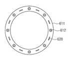
측정 유닛(600)은 챔버(100) 내부의 처리 공간 내에 노출된 노출 면을 가지는 부품의 소모 상태를 측정하여 부품의 교체 시기를 판단한다. 일 실시 예에 따르면, 부품의 노출 면은 방사 물질로 코팅되게 제공된다. 방사 물질은 조사 광에 반응 하여 방출 광을 방사하는 물질 일 수 있다. 예를 들면, 방사 물질은 산화 이트륨(Y2O3)을 포함하는 물질 일 수 있다. 산화 이트륨(Y2O3)은 자외선에 반응하여 적색 광을 방사한다. 예를 들면, 처리 공간 내에 노출된 노출 면을 가지는 부품은 포커스 링(240)일 수 있다. 이와 달리, 처리 공간 내에 노출된 노출 면을 가지는 부품은 라이너(130), 지지판 등 처리 공간 내에 노출된 노출 면을 가지고 플라스마에 의해 손상 가능성이 있어 교체가 예정된 다양한 종류의 부품일 수 있다. 도 4는 도 3의 반송 부재(700)에 지지된 조사 부재(610)의 저면을 나타낸 사시도이다. 도 2 내지 도 4를 참고하면, 측정 유닛(600)은 조사 부재(610), 수광 부재(620) 및 판단 부재(630)를 포함한다.The
조사 부재(610)는 챔버(100) 내부의 처리 공간 내에 노출된 노출 면을 가지는 부품에 조사 광을 조사한다. 조사 광은 자외선을 포함할 수 있다. 조사 부재(610)는 몸체(611) 및 발광 부재(612)를 포함한다.The
일 실시 예에 따르면, 몸체(611)는 상부에서 바라볼 때, 링 형상을 가지는 판 형상으로 제공될 수 있다. 이와 달리 몸체(611)는 기판을 반송시키는 반송 부재(700) 또는 기판을 지지하는 리프트 핀(도 6의 290)에 의해 지지되고, 기판 출입구(140)에 의해 챔버(100) 내부의 처리 공간으로 출입될 수 있는 다양한 형태로 제공될 수 있다.According to one embodiment, the
발광 부재(612)는 조사 광을 발생시킨다. 발광 부재(612)는 몸체(611)에 제공된다. 예를 들면, 조사 광이 조사되는 부품이 몸체(611)의 하부에 제공되는 경우, 발광 부재(612)는 몸체(611)의 하면에 제공될 수 있다. 이와 달리, 조사 광이 조사되는 부품이 몸체(611)의 상부에 제공되는 경우, 발광 부재(612)는 몸체(611)의 상면에 제공될 수 있다. 발광 부재(612)는 복수개로 제공될 수 있다. 복수개의 발광 부재(612)는 각각 서로 다른 파장의 조사광을 발생시킬 수 있다. 따라서, 조사광이 조사된 부품의 노출면이 발광 부재들 중 하나의 조사광의 파장에 대한 방출 광의 세기가 측정하기에 충분하지 않은 경우, 다른 파장의 조사 광을 조사하여 방출 광의 세기가 측정하기에 충분하도록 방출광을 방출되게 할 수 있다. 발광 부재(612)는 자외선을 발생시키는 발광다이오드(LED)로 제공될 수 있다. 발광 부재(612)는 전원을 제공하는 베터리(미도시)를 포함할 수 있다.The
기판 처리 장치(10)는 반송 부재(700)를 더 포함할 수 있다. 반송 부재(700)는 기판(W) 및 조사 부재(610)를 챔버(100) 내부의 처리 공간으로 반입 및 반출 시킨다. 일 실시 예에 따르면, 반송 부재(700)는 기판(W)이 챔버(100) 내부의 처리 공간으로 반입 및 반출되는 기판 출입구(140)를 통해 처리 공간으로 조사 부재(610)를 반입 및 반출시킨다. 따라서, 부품의 손상 정도 측정 시 커버(120)의 개폐가 요구되지 않으므로, 부품의 손상 정도를 측정하는 시간이 절감된다. 기판 출입구(140)는 하우징(110)의 측벽 및 라이너(130)의 측벽을 순차적으로 관통함으로써 형성될 수 있다. 기판 출입구(140)에 대향되는 하우징(110)의 외측면 또는 라이너(130)의 내측면에는 기판 출입구(140)를 개폐하는 도어가 제공된다.The
조사 부재(610)는 반송 부재(700)에 지지된 상태에서 챔버(100) 내부의 처리 공간 내에 노출된 노출 면을 가지는 부품에 조사광을 조사할 수 있다. 이 경우, 조사 부재(610)는 조사 부재(610)가 직접 놓이는 반송 부재(700)의 핸드부와 발광 부재(612)가 간섭되지 않도록 반송 부재(700)의 핸드부에 지지된다.The
도 5는 도 3의 조사 부재(610)가 리프트 핀(290)에 지지되는 모습을 나타낸 측면도이다. 도 5를 참고하면, 도 3 및 도 4의 경우와 달리, 조사 부재(610)는 리프트 핀(290)에 의해 지지된 상태에서 챔버(100) 내부의 처리 공간 내에 노출된 노출 면을 가지는 부품에 조사광을 조사할 수 있다.5 is a side view showing a state in which the
수광 부재(620)는 챔버(100) 내부의 처리 공간 내에 노출된 노출 면을 가지는 부품으로부터 방출되는 방출 광을 수광한다. 수광 부재(620)는 수광한 방출 광의 세기 등의 데이터를 판단 부재(630)로 전달한다.The
일 실시 예에 따르면, 수광 부재(620)는 종점 검출 장치를 포함한다. 종점 검출 장치는 기판(W)에 대한 공정 완료 시점을 검출한다. 이 경우, 종점 검출 장치는 부품으로부터 방출되는 방출 광을 수광한다. 따라서 별도의 방출 광을 수광하는 수단이 요구되지 않는다. 방출 광은 산화 이트륨(Y2O3)이 자외선에 반응하여 방사하는 적색 광일 수 있다.According to one embodiment, the
도 6은 본 발명의 다른 실시 예에 따른 몸체의 저면을 나타낸 저면도이다. 도 6을 참고하면 도 3 및 도 5의 경우와는 달리, 수광 부재(620)는 몸체(611)의 하면에 제공될 수 있다. 이 경우, 방출 광이 방사되는 부품은 몸체(611)의 하부에 제공된다. 이와 달리, 방출 광이 방사되는 부품이 몸체(611)의 상부에 제공되는 경우, 수광 부재(620)는 몸체(611)의 상면에 제공될 수 있다. 수광 부재(620)가 몸체(611)의 하면에 제공되는 경우, 수광 부재(620)는 포토 다이오드(Photo Diode)를 포함할 수 있다. 종점 검출 장치는 일반적으로 챔버 측벽에 형성된 채광 창 등을 통해 처리 공간으로부터 발생되는 빛을 수광하여 측정한다. 따라서, 채광 창이 반응 부산물 등에 의해 오염되는 경우, 측정의 정밀도가 저하된다. 그러므로 수광 부재(620)가 포토 다이오드를 이용하여 방출 광을 수광하는 경우, 보다 정밀한 측정이 가능하다.6 is a bottom view of the bottom of the body according to another embodiment of the present invention. Referring to FIG. 6, the
판단 부재(630)는 수광 부재(620)로부터 수광된 방출 광으로부터 부품의 상태를 판단한다. 예를 들면, 부품의 노출면이 산화 이트륨(Y2O3)으로 코팅된 경우, 노출 면에 자외선을 조사하면 자외선에 반응하여 코팅의 두께가 두꺼울수록 강한 세기의 적색 광을 방사한다. 따라서, 조사광이 자외선을 포함하는 경우, 노출 면은 코팅의 두께에 따라 상이한 세기의 방출 광을 방사한다. 이 경우, 판단 부재(630)는 수광된 방출 광의 세기로부터 부품의 노출면의 산화 이트륨(Y2O3) 코팅 두께의 상태를 판단한다. 즉, 판단 부재(630)는 방출 광의 세기가 설정 크기 이하이면 부품의 교체 시기가 도래된 것으로 판단한다.The
이하, 본 발명에 실시 예에 따른 기판 처리 방법을 설명한다. 설명의 편의를 위해 상술한 기판 처리 장치를 이용하여 수행되는 것으로 가정한다.Hereinafter, a substrate processing method according to an embodiment of the present invention will be described. It is assumed that the above-described substrate processing apparatus is used for convenience of explanation.
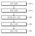
도 7은 본 발명의 일 실시 예에 따른 기판 처리 방법을 나타낸 순서도이다. 도 7을 참고하면, 기판 처리 방법은 지지 단계(S01a), 반입 단계(S01b), 조사광 조사 단계(S02), 판단 단계(S03) 및 공정 단계(S04)를 포함한다.7 is a flowchart illustrating a substrate processing method according to an embodiment of the present invention. 7, the substrate processing method includes a support step S01a, a carry-in step S01b, an irradiation light irradiation step S02, a determination step S03, and a processing step S04.
지지 단계(S01a)에서는 반송 부재(700)가 챔버(100)의 처리 공간의 외부에서 조사 부재(610)를 지지한다.In the supporting step S01a, the conveying
이 후, 반입 단계(S01b)에서는 반송 부재(700)가 조사 부재(610)를 챔버(100) 내부의 처리 공간으로 반입시킨다.Thereafter, in the carrying-in step S01b, the carrying
이 후, 조사광 조사 단계(S02)에서는 기판(W)이 처리되는 처리 공간 내에 노출된 노출 면을 가지는 부품에 조사 광을 조사한다. 예를 들면, 도 3의 경우와 같이, 조사 부재(610)는 반송 부재(700)에 지지된 상태에서 처리 공간 내에 노출된 노출면을 가지는 부품에 조사 광을 조사한다.Thereafter, in the irradiation light irradiation step S02, irradiation light is irradiated onto the component having the exposed surface exposed in the processing space in which the substrate W is processed. For example, as in the case of Fig. 3, the
판단 단계(S03)에서는 조사 광에 반응하여 처리 공간 내에 노출된 노출 면을 가지는 부품의 노출 면이 방사하는 방출 광으로부터 부품의 상태를 판단한다. 일 실시 예에 따르면, 부품의 노출면은 조사 광에 반응하여 방출광을 방사하는 방사 물질로 코팅되고, 판단 단계(S03)에서는 조사 부재(610)에 의해 조사된 조사광에 반응하여 노출 면이 방사하는 방출 광을 수광 부재(620)가 수광한다. 이 후, 수광 부재(620)는 방출 광의 세기 등의 데이터를 판단 부재(630)로 전달한다. 판단 부재(630)는 수광 부재(620)로부터 전달받은 방출 광의 세기로부터 노출 면의 코팅의 두께의 상태를 판단한다. 예를 들면, 판단 단계(S03)에서는 판단 부재(630)가 방출 광의 세기가 설정 크기 이하이면 부품의 교체 시기가 도래된 것으로 판단하여 공정 단계(S04) 이전에 부품을 교체 또는 수리한다.In the determination step S03, the state of the component is determined from the emitted light emitted from the exposed surface of the component having the exposed surface exposed in the processing space in response to the irradiated light. According to one embodiment, the exposed surface of the component is coated with a spinning material that emits emission light in response to the irradiation light, and in the determining step S03, the exposed surface in response to the irradiation light irradiated by the
이 후, 공정 단계(S04)에서는 플라스마를 이용하여 챔버(100)의 처리 공간 내에 제공된 기판(W)을 처리하는 공정이 수행된다.Thereafter, in process step S04, a process of processing the substrate W provided in the processing space of the
도 8은 본 발명의 다른 실시 예에 따른 기판 처리 방법을 나타낸 순서도이다. 도 8을 참고하면, 도 7의 경우와 달리, 기판 처리 방법은 반입 단계(S01b)와 조사광 조사 단계(S02)의 사이에 인수 단계(S01c)를 더 포함한다. 인수 단계(S01c)에서는 리프트 핀(290)은 조사 부재(610)를 반입시킨 반송 부재(700)로부터 조사 부재(610)를 이전 받는다. 이 경우, 조사광 조사 단계(S02)에서는 조사 부재(610)가 리프트 핀(290)에 지지된 상태에서 부품에 조사 광을 조사한다. 그 외의 이용되는 장치의 구성, 구조 및 공정 등은 도 7의 경우와 유사하다.8 is a flowchart illustrating a substrate processing method according to another embodiment of the present invention. Referring to Fig. 8, unlike the case of Fig. 7, the substrate processing method further includes a step S01c between the carrying-in step S01b and the irradiating light applying step S02. In the acquisition step S01c, the
상술한 바와 같이, 본 발명의 실시 예에 따른 기판 처리 장치 및 기판 처리 방법은 부품의 표면에 조사 광을 조사하여 조사광에 반응하여 부품이 방사하는 방출 광의 세기로부터 부품의 교체 손상 정도를 측정할 수 있으므로, 기판 처리 장치 내에 제공된 부품의 손상 정도를 정밀하게 측정할 수 있다. 따라서, 본 발명의 실시 예에 따른 장치 및 방법은 기판 처리 공정을 정밀하게 제어할 수 있다. 또한, 조사광을 조사하는 조사 부재(610)가 반송 부재에 의해 기판 출입구를 통해 처리 공간으로 반입 및 반출될 수 있으므로 처리 공간 상부를 덮는 커버(120)를 개방할 필요가 없어 기판 처리 장치 내에 제공된 부품의 손상 정도를 측정하는 시간을 절감할 수 있다.As described above, in the substrate processing apparatus and the substrate processing method according to the embodiment of the present invention, irradiation light is irradiated to the surface of a component, and the degree of replacement damage of the component is measured from the intensity of emitted light emitted by the component in response to the irradiation light It is possible to precisely measure the degree of damage of the parts provided in the substrate processing apparatus. Therefore, the apparatus and method according to the embodiment of the present invention can precisely control the substrate processing process. Further, since the
10: 기판 처리 장치W: 기판
100: 챔버200: 지지 유닛
240: 포커스 링290: 리프트 핀
300: 가스 공급 유닛400: 플라스마 소스
500: 배기 유닛600: 측정 유닛
610: 조사 부재620: 수광 부재
630: 판단 부재700: 반송 부재10: substrate processing apparatus W: substrate
100: chamber 200: support unit
240: focus ring 290: lift pin
300: gas supply unit 400: plasma source
500: exhaust unit 600: measuring unit
610: Irradiation member 620: Light receiving member
630: judging member 700: conveying member
Claims (28)
Translated fromKorean내부에 처리 공간을 가지는 챔버와;
상기 처리 공간 내에 배치되며 기판이 놓이는 지지판을 가지는 지지 유닛과;
상기 처리 공간 내로 공정 가스를 공급하는 가스 공급 유닛과;
상기 처리 공간의 외부에 제공되며, 상기 처리 공간 내의 공정 가스로부터 플라스마를 생성하는 플라스마 소스와;
상기 처리 공간 내에 노출된 노출면을 가지는 부품의 소모 상태를 측정하는 측정 유닛을 포함하되,
상기 측정 유닛은,
상기 부품에 조사 광을 조사하는 조사 부재와;
상기 부품으로부터 방출되는 방출 광을 수광하여 상기 방출 광의 세기를 측정하는 수광 부재와;
상기 방출 광의 세기에 기초하여 상기 부품의 상태를 판단하는 판단 부재;를 포함하고,
상기 노출 면은 상기 조사 광에 반응하여 상기 방출 광을 방사하는 방사 물질로 코팅되며,
상기 조사 부재는,
판 형상을 가지는 몸체 및 상기 몸체에 제공되고 상기 조사 광을 발생시키는 발광 부재를 포함하고,
상기 발광 부재는,
복수 개 제공되고, 각각 서로 다른 파장의 조사 광을 발생시키는 기판 처리 장치.An apparatus for processing a substrate,
A chamber having a processing space therein;
A support unit disposed in the processing space and having a support plate on which the substrate is placed;
A gas supply unit for supplying a process gas into the process space;
A plasma source provided outside of the processing space and generating a plasma from the processing gas in the processing space;
And a measurement unit for measuring the consumption state of the component having the exposed surface exposed in the processing space,
Wherein the measuring unit comprises:
An irradiation member for irradiating the component with irradiation light;
A light receiving member for receiving the emitted light emitted from the component and measuring the intensity of the emitted light;
And a determination member for determining the state of the component based on the intensity of the emitted light,
Wherein the exposed surface is coated with a spinning material that emits the emitted light in response to the irradiating light,
The irradiation member
A body having a plate shape, and a light emitting member provided on the body and generating the irradiation light,
The light-
A plurality of substrate processing apparatuses are provided, each of which generates irradiation light of a different wavelength.
상기 기판 처리 장치는 상기 처리 공간 내로 기판을 반입 및 반출하는 반송 부재를 더 포함하되,
상기 조사 부재는 상기 반송 부재에 지지되는 기판 처리 장치.The method according to claim 1,
The substrate processing apparatus further includes a transporting member for transporting the substrate into and out of the processing space,
And the irradiation member is supported on the carrying member.
상기 지지 유닛은 외부의 반송 부재로부터 기판을 전달받아 상기 지지 판으로 안착시키는 리프트 핀;을 더 포함하되,
상기 조사 부재는 상기 리프트 핀에 의해 지지되는 기판 처리 장치.The method according to claim 1,
The supporting unit may further include a lift pin for receiving the substrate from an external conveying member and seating the substrate on the supporting plate,
Wherein the irradiation member is supported by the lift pins.
상기 수광 부재는 상기 몸체에 제공되는 기판 처리 장치.The method according to claim 1,
Wherein the light receiving member is provided on the body.
상기 수광 부재는 기판에 대한 공정 완료 시점을 검출하는 종점 검출 장치;를 포함하는 기판 처리 장치.4. The method according to any one of claims 1 to 3,
And the light receiving member includes an end point detection device for detecting a completion time of the process for the substrate.
상기 수광 부재는 포토 다이오드(Photo Diode)를 포함하는 기판 처리 장치.4. The method according to any one of claims 1 to 3,
Wherein the light receiving member includes a photodiode.
상기 방사 물질은 산화 이트륨(Y2O3)을 포함하는 기판 처리 장치.The method according to claim 1,
The radiation material is a substrate processing apparatus including a yttrium oxide (Y2 O3).
상기 부품의 상태는 상기 코팅의 두께의 상태를 포함하는 기판 처리 장치.The method according to claim 1,
Wherein the state of the part comprises a state of thickness of the coating.
상기 판단 부재는 상기 방출 광의 세기가 설정 크기 이하이면 상기 부품의 교체 시기가 도래된 것으로 판단하는 기판 처리 장치.4. The method according to any one of claims 1 to 3,
Wherein the determining member determines that the replacement timing of the component has arrived when the intensity of the emitted light is equal to or smaller than a predetermined magnitude.
상기 조사 광은 자외선을 포함하는 기판 처리 장치.4. The method according to any one of claims 1 to 3,
Wherein the irradiation light includes ultraviolet rays.
상기 지지 유닛은 상기 지지판을 둘러싸도록 제공된 포커스 링을 더 포함하고,
상기 부품은 상기 포커스 링을 포함하는 기판 처리 장치.4. The method according to any one of claims 1 to 3,
Wherein the support unit further comprises a focus ring provided to surround the support plate,
Wherein the component comprises the focus ring.
상기 방출 광은 적색광을 포함하는 기판 처리 장치.4. The method according to any one of claims 1 to 3,
Wherein the emitted light comprises red light.
상기 조사 광에 반응하여 상기 노출 면이 방사하는 방출 광의 세기를 측정하는 단계; 및
상기 방출 광의 세기에 기초하여 상기 부품의 상태를 판단하는 판단 단계;를 포함하고,
상기 노출 면은 상기 조사 광에 반응하여 상기 방출 광을 방사하는 방사 물질로 코팅되며,
상기 조사광 조사 단계는, 상기 부품에 서로 다른 파장의 복수의 조사 광을 조사하는 기판 처리 방법.An irradiation light irradiation step of irradiating irradiation light to a part having an exposed surface exposed in a processing space in which the substrate is processed;
Measuring the intensity of the emitted light emitted by the exposed surface in response to the irradiated light; And
And determining a state of the component based on the intensity of the emitted light,
Wherein the exposed surface is coated with a spinning material that emits the emitted light in response to the irradiating light,
Wherein the irradiating light irradiation step irradiates the component with a plurality of irradiating lights of different wavelengths.
상기 조사광 조사 단계에서는 조사 부재가 반송 부재에 지지된 상태에서 상기 부품에 조사 광을 조사하는 기판 처리 방법.19. The method of claim 18,
And the irradiation light is irradiated to the component while the irradiation member is supported on the carrying member in the irradiation light irradiation step.
상기 조사광 조사 단계에서는 조사 부재가 리프트 핀에 지지된 상태에서 상기 부품에 조사 광을 조사하는 기판 처리 방법.19. The method of claim 18,
And the irradiation light is irradiated to the component while the irradiation member is supported by the lift pin in the irradiation light irradiation step.
상기 조사광 조사 단계 이전에 이전 단계;를 더 포함하되,
상기 이전 단계에서는 상기 리프트 핀이 반송 부재로부터 상기 조사광을 조사하는 조사 부재를 이전 받는 기판 처리 방법.21. The method of claim 20,
Further comprising a preceding step before the irradiating light irradiation step,
Wherein in the preceding step, the lift pin transfers the irradiation member for irradiating the irradiation light from the carrying member.
상기 조사 광 조사 단계 이전에,
반송 부재가 상기 처리 공간의 외부에서 조사 부재를 지지하는 지지 단계; 및
상기 반송 부재가 상기 조사 부재를 상기 처리 공간으로 반입시키는 반입 단계;를 더 포함하는 기판 처리 방법.19. The method of claim 18,
Before the irradiation light irradiation step,
A supporting step in which the conveying member supports the irradiation member outside the processing space; And
And a carrying-in step in which the carrying member brings the irradiation member into the processing space.
상기 판단 단계에서는 상기 코팅의 두께의 상태를 판단하는 기판 처리 방법.19. The method of claim 18,
Wherein the determining step determines the thickness of the coating.
상기 판단 단계에서는 상기 방출 광의 세기가 설정 크기 이하이면 상기 부품의 교체 시기가 도래된 것으로 판단하는 기판 처리 방법.22. The method according to any one of claims 18 to 21,
Wherein the determining step determines that the replacement time of the component has arrived when the intensity of the emitted light is less than a set magnitude.
상기 판단 단계 이 후에는,
플라스마를 이용하여 상기 처리 공간 내에 제공된 기판을 처리 하는 공정이 수행되는 공정 단계;를 더 포함하는 기판 처리 방법.
22. The method according to any one of claims 18 to 21,
After the determining step,
And a processing step of processing the substrate provided in the processing space by using plasma.
Priority Applications (1)
| Application Number | Priority Date | Filing Date | Title |
|---|---|---|---|
| KR1020150045452AKR101870649B1 (en) | 2015-03-31 | 2015-03-31 | Apparatus and method for treating substrate |
Applications Claiming Priority (1)
| Application Number | Priority Date | Filing Date | Title |
|---|---|---|---|
| KR1020150045452AKR101870649B1 (en) | 2015-03-31 | 2015-03-31 | Apparatus and method for treating substrate |
Publications (2)
| Publication Number | Publication Date |
|---|---|
| KR20160117822A KR20160117822A (en) | 2016-10-11 |
| KR101870649B1true KR101870649B1 (en) | 2018-06-27 |
Family
ID=57161755
Family Applications (1)
| Application Number | Title | Priority Date | Filing Date |
|---|---|---|---|
| KR1020150045452AActiveKR101870649B1 (en) | 2015-03-31 | 2015-03-31 | Apparatus and method for treating substrate |
Country Status (1)
| Country | Link |
|---|---|
| KR (1) | KR101870649B1 (en) |
Citations (1)
| Publication number | Priority date | Publication date | Assignee | Title |
|---|---|---|---|---|
| JP2004263283A (en)* | 2003-03-04 | 2004-09-24 | Konica Minolta Holdings Inc | Etching method and etching system |
Family Cites Families (6)
| Publication number | Priority date | Publication date | Assignee | Title |
|---|---|---|---|---|
| WO2004081140A1 (en)* | 2003-03-13 | 2004-09-23 | Nichia Corporation | Light emitting film, luminescent device, method for manufacturing light emitting film and method for manufacturing luminescent device |
| US8343305B2 (en)* | 2007-09-04 | 2013-01-01 | Lam Research Corporation | Method and apparatus for diagnosing status of parts in real time in plasma processing equipment |
| US20090151870A1 (en)* | 2007-12-14 | 2009-06-18 | Tokyo Electron Limited | Silicon carbide focus ring for plasma etching system |
| US20110117728A1 (en)* | 2009-08-27 | 2011-05-19 | Applied Materials, Inc. | Method of decontamination of process chamber after in-situ chamber clean |
| JP2011210853A (en)* | 2010-03-29 | 2011-10-20 | Tokyo Electron Ltd | Method for measuring wear rate |
| JP6231370B2 (en)* | 2013-12-16 | 2017-11-15 | 東京エレクトロン株式会社 | Consumption amount measuring device, temperature measuring device, consumption amount measuring method, temperature measuring method, and substrate processing system |
- 2015
- 2015-03-31KRKR1020150045452Apatent/KR101870649B1/enactiveActive
Patent Citations (1)
| Publication number | Priority date | Publication date | Assignee | Title |
|---|---|---|---|---|
| JP2004263283A (en)* | 2003-03-04 | 2004-09-24 | Konica Minolta Holdings Inc | Etching method and etching system |
Also Published As
| Publication number | Publication date |
|---|---|
| KR20160117822A (en) | 2016-10-11 |
Similar Documents
| Publication | Publication Date | Title |
|---|---|---|
| US11062885B2 (en) | Supporting unit and substrate treating apparatus including the same | |
| KR101559024B1 (en) | Apparatus for treating substrate | |
| KR101951369B1 (en) | Electrostatic chuck and substrate treating apparatus including the chuck | |
| KR102330281B1 (en) | Electrostatic chuck and substrate treating apparatus including the chuck | |
| KR101974419B1 (en) | Window unit, apparatus for treating substrate comprising the same, method for treating substrate, and manufacturing method of the same | |
| KR102278077B1 (en) | Supporting unit and apparatus and method for treating substrate comprising the same | |
| KR102862134B1 (en) | Apparatus for treating substrate | |
| CN108695132B (en) | Plasma generation unit and substrate processing apparatus including the same | |
| KR101842123B1 (en) | Apparatus for treating substrate | |
| KR101791870B1 (en) | Inspecting method, apparatus and method for treating substrate including the same | |
| KR101870649B1 (en) | Apparatus and method for treating substrate | |
| KR102186071B1 (en) | Apparatus and method for treating substrate | |
| KR20160134921A (en) | Apparatus for treating substrate, method for detecting lift pin alignment and method for detecting whether electrostatic force is applied | |
| US20230030464A1 (en) | Support unit, apparatus for treating substrate with the same and method for treating substrate with the same | |
| KR102330280B1 (en) | Apparatus for treating substrate and method for replacing component | |
| KR101408787B1 (en) | Apparatus for treating substrate | |
| KR101502853B1 (en) | Supporting unit and apparatus for treating substrate | |
| KR102757465B1 (en) | Substrate processing apparatus and method | |
| KR20160054146A (en) | Apparatus for treating substrate | |
| KR20170025472A (en) | Supporting unit and substrate treating apparatus including the chuck | |
| KR20170026819A (en) | Apparatus and method for treating a substrate | |
| KR101934985B1 (en) | Apparatus for treating substrate and method for stabilizing surface of the apparatus | |
| KR101632606B1 (en) | Method and apparatus for treating substrate | |
| KR101632605B1 (en) | Method and apparatus for treating substrate | |
| KR20180003781A (en) | Apparatus for treating substrate |
Legal Events
| Date | Code | Title | Description |
|---|---|---|---|
| A201 | Request for examination | ||
| PA0109 | Patent application | Patent event code:PA01091R01D Comment text:Patent Application Patent event date:20150331 | |
| PA0201 | Request for examination | ||
| PG1501 | Laying open of application | ||
| AMND | Amendment | ||
| E601 | Decision to refuse application | ||
| PE0601 | Decision on rejection of patent | Patent event date:20170426 Comment text:Decision to Refuse Application Patent event code:PE06012S01D Patent event date:20161031 Comment text:Notification of reason for refusal Patent event code:PE06011S01I | |
| AMND | Amendment | ||
| PX0901 | Re-examination | Patent event code:PX09011S01I Patent event date:20170426 Comment text:Decision to Refuse Application Patent event code:PX09012R01I Patent event date:20161230 Comment text:Amendment to Specification, etc. | |
| E902 | Notification of reason for refusal | ||
| PE0902 | Notice of grounds for rejection | Comment text:Notification of reason for refusal Patent event date:20170707 Patent event code:PE09021S01D | |
| AMND | Amendment | ||
| PX0701 | Decision of registration after re-examination | Patent event date:20180611 Comment text:Decision to Grant Registration Patent event code:PX07013S01D Patent event date:20171207 Comment text:Amendment to Specification, etc. Patent event code:PX07012R01I Patent event date:20170529 Comment text:Amendment to Specification, etc. Patent event code:PX07012R01I Patent event date:20170426 Comment text:Decision to Refuse Application Patent event code:PX07011S01I Patent event date:20161230 Comment text:Amendment to Specification, etc. Patent event code:PX07012R01I | |
| X701 | Decision to grant (after re-examination) | ||
| GRNT | Written decision to grant | ||
| PR0701 | Registration of establishment | Comment text:Registration of Establishment Patent event date:20180619 Patent event code:PR07011E01D | |
| PR1002 | Payment of registration fee | Payment date:20180620 End annual number:3 Start annual number:1 | |
| PG1601 | Publication of registration | ||
| PR1001 | Payment of annual fee | Payment date:20210325 Start annual number:4 End annual number:4 | |
| PR1001 | Payment of annual fee | Payment date:20220525 Start annual number:5 End annual number:5 |