KR101869157B1 - Sensor cover laminates for vehicle adjusting color and penetrating electronic waves - Google Patents
Sensor cover laminates for vehicle adjusting color and penetrating electronic wavesDownload PDFInfo
- Publication number
- KR101869157B1 KR101869157B1KR1020160109354AKR20160109354AKR101869157B1KR 101869157 B1KR101869157 B1KR 101869157B1KR 1020160109354 AKR1020160109354 AKR 1020160109354AKR 20160109354 AKR20160109354 AKR 20160109354AKR 101869157 B1KR101869157 B1KR 101869157B1
- Authority
- KR
- South Korea
- Prior art keywords
- layer
- germanium
- refractive index
- zinc compound
- thickness
- Prior art date
- Legal status (The legal status is an assumption and is not a legal conclusion. Google has not performed a legal analysis and makes no representation as to the accuracy of the status listed.)
- Active
Links
Images


Classifications
- C—CHEMISTRY; METALLURGY
- C23—COATING METALLIC MATERIAL; COATING MATERIAL WITH METALLIC MATERIAL; CHEMICAL SURFACE TREATMENT; DIFFUSION TREATMENT OF METALLIC MATERIAL; COATING BY VACUUM EVAPORATION, BY SPUTTERING, BY ION IMPLANTATION OR BY CHEMICAL VAPOUR DEPOSITION, IN GENERAL; INHIBITING CORROSION OF METALLIC MATERIAL OR INCRUSTATION IN GENERAL
- C23C—COATING METALLIC MATERIAL; COATING MATERIAL WITH METALLIC MATERIAL; SURFACE TREATMENT OF METALLIC MATERIAL BY DIFFUSION INTO THE SURFACE, BY CHEMICAL CONVERSION OR SUBSTITUTION; COATING BY VACUUM EVAPORATION, BY SPUTTERING, BY ION IMPLANTATION OR BY CHEMICAL VAPOUR DEPOSITION, IN GENERAL
- C23C14/00—Coating by vacuum evaporation, by sputtering or by ion implantation of the coating forming material
- C23C14/06—Coating by vacuum evaporation, by sputtering or by ion implantation of the coating forming material characterised by the coating material
- C23C14/0623—Sulfides, selenides or tellurides
- C23C14/0629—Sulfides, selenides or tellurides of zinc, cadmium or mercury
- H—ELECTRICITY
- H01—ELECTRIC ELEMENTS
- H01Q—ANTENNAS, i.e. RADIO AERIALS
- H01Q1/00—Details of, or arrangements associated with, antennas
- H01Q1/42—Housings not intimately mechanically associated with radiating elements, e.g. radome
- B—PERFORMING OPERATIONS; TRANSPORTING
- B05—SPRAYING OR ATOMISING IN GENERAL; APPLYING FLUENT MATERIALS TO SURFACES, IN GENERAL
- B05D—PROCESSES FOR APPLYING FLUENT MATERIALS TO SURFACES, IN GENERAL
- B05D1/00—Processes for applying liquids or other fluent materials
- B05D1/62—Plasma-deposition of organic layers
- B—PERFORMING OPERATIONS; TRANSPORTING
- B60—VEHICLES IN GENERAL
- B60R—VEHICLES, VEHICLE FITTINGS, OR VEHICLE PARTS, NOT OTHERWISE PROVIDED FOR
- B60R13/00—Elements for body-finishing, identifying, or decorating; Arrangements or adaptations for advertising purposes
- B60R13/005—Manufacturers' emblems, name plates, bonnet ornaments, mascots or the like; Mounting means therefor
- B—PERFORMING OPERATIONS; TRANSPORTING
- B60—VEHICLES IN GENERAL
- B60R—VEHICLES, VEHICLE FITTINGS, OR VEHICLE PARTS, NOT OTHERWISE PROVIDED FOR
- B60R19/00—Wheel guards; Radiator guards, e.g. grilles; Obstruction removers; Fittings damping bouncing force in collisions
- B60R19/52—Radiator or grille guards ; Radiator grilles
- C—CHEMISTRY; METALLURGY
- C23—COATING METALLIC MATERIAL; COATING MATERIAL WITH METALLIC MATERIAL; CHEMICAL SURFACE TREATMENT; DIFFUSION TREATMENT OF METALLIC MATERIAL; COATING BY VACUUM EVAPORATION, BY SPUTTERING, BY ION IMPLANTATION OR BY CHEMICAL VAPOUR DEPOSITION, IN GENERAL; INHIBITING CORROSION OF METALLIC MATERIAL OR INCRUSTATION IN GENERAL
- C23C—COATING METALLIC MATERIAL; COATING MATERIAL WITH METALLIC MATERIAL; SURFACE TREATMENT OF METALLIC MATERIAL BY DIFFUSION INTO THE SURFACE, BY CHEMICAL CONVERSION OR SUBSTITUTION; COATING BY VACUUM EVAPORATION, BY SPUTTERING, BY ION IMPLANTATION OR BY CHEMICAL VAPOUR DEPOSITION, IN GENERAL
- C23C14/00—Coating by vacuum evaporation, by sputtering or by ion implantation of the coating forming material
- C23C14/06—Coating by vacuum evaporation, by sputtering or by ion implantation of the coating forming material characterised by the coating material
- C23C14/14—Metallic material, boron or silicon
- C23C14/18—Metallic material, boron or silicon on other inorganic substrates
- C—CHEMISTRY; METALLURGY
- C23—COATING METALLIC MATERIAL; COATING MATERIAL WITH METALLIC MATERIAL; CHEMICAL SURFACE TREATMENT; DIFFUSION TREATMENT OF METALLIC MATERIAL; COATING BY VACUUM EVAPORATION, BY SPUTTERING, BY ION IMPLANTATION OR BY CHEMICAL VAPOUR DEPOSITION, IN GENERAL; INHIBITING CORROSION OF METALLIC MATERIAL OR INCRUSTATION IN GENERAL
- C23C—COATING METALLIC MATERIAL; COATING MATERIAL WITH METALLIC MATERIAL; SURFACE TREATMENT OF METALLIC MATERIAL BY DIFFUSION INTO THE SURFACE, BY CHEMICAL CONVERSION OR SUBSTITUTION; COATING BY VACUUM EVAPORATION, BY SPUTTERING, BY ION IMPLANTATION OR BY CHEMICAL VAPOUR DEPOSITION, IN GENERAL
- C23C14/00—Coating by vacuum evaporation, by sputtering or by ion implantation of the coating forming material
- C23C14/22—Coating by vacuum evaporation, by sputtering or by ion implantation of the coating forming material characterised by the process of coating
- C23C14/24—Vacuum evaporation
- C23C14/28—Vacuum evaporation by wave energy or particle radiation
- H—ELECTRICITY
- H01—ELECTRIC ELEMENTS
- H01Q—ANTENNAS, i.e. RADIO AERIALS
- H01Q1/00—Details of, or arrangements associated with, antennas
- H01Q1/02—Arrangements for de-icing; Arrangements for drying-out ; Arrangements for cooling; Arrangements for preventing corrosion
- H—ELECTRICITY
- H01—ELECTRIC ELEMENTS
- H01Q—ANTENNAS, i.e. RADIO AERIALS
- H01Q1/00—Details of, or arrangements associated with, antennas
- H01Q1/27—Adaptation for use in or on movable bodies
- H01Q1/32—Adaptation for use in or on road or rail vehicles
- H01Q1/3208—Adaptation for use in or on road or rail vehicles characterised by the application wherein the antenna is used
- H01Q1/3233—Adaptation for use in or on road or rail vehicles characterised by the application wherein the antenna is used particular used as part of a sensor or in a security system, e.g. for automotive radar, navigation systems
- H—ELECTRICITY
- H01—ELECTRIC ELEMENTS
- H01Q—ANTENNAS, i.e. RADIO AERIALS
- H01Q1/00—Details of, or arrangements associated with, antennas
- H01Q1/42—Housings not intimately mechanically associated with radiating elements, e.g. radome
- H01Q1/422—Housings not intimately mechanically associated with radiating elements, e.g. radome comprising two or more layers of dielectric material
- H—ELECTRICITY
- H01—ELECTRIC ELEMENTS
- H01Q—ANTENNAS, i.e. RADIO AERIALS
- H01Q1/00—Details of, or arrangements associated with, antennas
- H01Q1/42—Housings not intimately mechanically associated with radiating elements, e.g. radome
- H01Q1/425—Housings not intimately mechanically associated with radiating elements, e.g. radome comprising a metallic grid
- B—PERFORMING OPERATIONS; TRANSPORTING
- B60—VEHICLES IN GENERAL
- B60R—VEHICLES, VEHICLE FITTINGS, OR VEHICLE PARTS, NOT OTHERWISE PROVIDED FOR
- B60R13/00—Elements for body-finishing, identifying, or decorating; Arrangements or adaptations for advertising purposes
- B60R13/04—External Ornamental or guard strips; Ornamental inscriptive devices thereon
- B—PERFORMING OPERATIONS; TRANSPORTING
- B60—VEHICLES IN GENERAL
- B60R—VEHICLES, VEHICLE FITTINGS, OR VEHICLE PARTS, NOT OTHERWISE PROVIDED FOR
- B60R19/00—Wheel guards; Radiator guards, e.g. grilles; Obstruction removers; Fittings damping bouncing force in collisions
- B60R19/52—Radiator or grille guards ; Radiator grilles
- B60R2019/525—Radiator grilles
- H—ELECTRICITY
- H01—ELECTRIC ELEMENTS
- H01Q—ANTENNAS, i.e. RADIO AERIALS
- H01Q1/00—Details of, or arrangements associated with, antennas
- H01Q1/27—Adaptation for use in or on movable bodies
- H01Q1/32—Adaptation for use in or on road or rail vehicles
- H01Q1/325—Adaptation for use in or on road or rail vehicles characterised by the location of the antenna on the vehicle
- H01Q1/3291—Adaptation for use in or on road or rail vehicles characterised by the location of the antenna on the vehicle mounted in or on other locations inside the vehicle or vehicle body
Landscapes
- Engineering & Computer Science (AREA)
- Chemical & Material Sciences (AREA)
- Mechanical Engineering (AREA)
- Organic Chemistry (AREA)
- Metallurgy (AREA)
- Chemical Kinetics & Catalysis (AREA)
- Materials Engineering (AREA)
- Computer Security & Cryptography (AREA)
- Radar, Positioning & Navigation (AREA)
- Remote Sensing (AREA)
- Health & Medical Sciences (AREA)
- Inorganic Chemistry (AREA)
- Toxicology (AREA)
- Physics & Mathematics (AREA)
- Plasma & Fusion (AREA)
- Laminated Bodies (AREA)
- Physical Vapour Deposition (AREA)
Abstract
Translated fromKoreanDescription
Translated fromKorean본 발명은, 적층체에 관한 것으로, 더욱 상세하게는, 저마늄층, 유기물층, 아연화합물층 등을 구비하여 특정한 색상 및 광택을 나타내고, 전파를 투과시킬 수 있으며, 내수성이 우수한 적층체에 관한 것이다. 본 발명은 국제특허분류(International Patent Classification, IPC)상 B32B 5에 해당된다.The present invention relates to a laminate, and more particularly, to a laminate which has a lowermanium layer, an organic layer, a zinc compound layer and the like to exhibit a specific color and gloss, can transmit radio waves, and is excellent in water resistance. The present invention corresponds to
센서 커버(Sensor cover)는 센서(Sensor)의 안테나를 덮는 부분으로, 통상 안테나를 충돌, 파편, 및 강한 풍압으로부터 보호하기 위해 설치된다. 따라서 센서 커버에는 풍압, 공기와의 마찰, 우박 등에 견딜 수 있는 강도, 내후성, 경량성, 우수한 전파 투과율 등이 요구된다.The sensor cover covers the antenna of the sensor and is usually installed to protect the antenna from impact, debris, and strong wind pressure. Therefore, the sensor cover is required to have strength against wind pressure, friction with air, hail, weather resistance, light weight, and excellent radio wave transmittance.
그런데 센서 커버를 설계하는데 디자인 측면에서 제약을 받는 경우가 있다. 오토 크루즈 컨트롤 시스템(auto cruise control system)은, 운전자가 희망하는 속도로 스위치를 조작하면, 컴퓨터가 차속을 기억하여 운전자가 엑셀 페달을 밟지 않고도 차량이 주행할 수 있게 하는 장치를 말한다. 오토 크루즈 컨트롤 시스템은 차속뿐만 아니라 차량 간 거리도 제어하는데, 시스템에 설치된 센서가 차량 간 거리를 감지할 수 있다. 차량 간 거리를 감지하기 위한 센서는 차량의 앞쪽에 설치될 수 밖에 없고, 미관상 센서의 안테나를 덮을 수 있는 센서 커버가 요구된다. 그리고 차량용 센서 커버는 그 주변과 어우러질 필요가 있다.However, there are cases where the design of the sensor cover is limited by the design aspect. An auto cruise control system is a device that allows a computer to memorize a vehicle speed when the driver operates the switch at a desired speed and allows the vehicle to travel without the driver stepping on the accelerator pedal. The autocruise control system not only controls the vehicle speed but also the vehicle-to-vehicle distance, sensors installed in the system can detect the distance between vehicles. A sensor for detecting the distance between the vehicles can not but be installed in front of the vehicle, and a sensor cover for covering the antenna of the cosmetic sensor is required. And the vehicle sensor cover needs to be aligned with its surroundings.
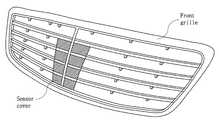
도 1에는 앞쪽 내부에 센서가 설치된 차량의 예시를 나타내는 사시도가 도시되어 있다. 차량용 센서 커버는 프론트 그릴(Front grille)에 설치되거나, 엠블럼(Emblem) 뒷면에 설치되거나, 또는 엠블럼 그 자체가 될 수 있다. 도 2 및 도 3에는 차량용 센서 커버가 설치된 프론트 그릴의 예시를 나타내는 사시도가 도시되어 있다. 도 2에서, 차량용 센서 커버는 프론트 그릴의 중앙에 설치되어 있다. 그리고 도 3에서는, 차량용 센서 커버가 그 자체로 엠블럼이 되어 있다. 통상적으로, 프론트 그릴은 흑색 및/또는 은색을 나타낸다. 엠블럼도 흑색 및/또는 은색을 나타내는 경우가 대부분이다. 따라서 전파 투과성을 확보하기 위해 투명한 소재로 차량용 센서 커버를 제조할 경우, 그 차량용 센서 커버는 그 주변과 어우러지기 어렵다. 게다가 차량의 내부가 투명한 센서 커버를 통해 보여지는 것은 미관상 좋지 않다. 그러나 흑색 또는 은색을 나타내는 소재로 차량용 센서 커버를 제조할 경우, 그 차량용 센서 커버가 그 주변의 프론트 그릴 및/또는 엠블럼과 연속성이 있는 것은 별론, 전파 투과성을 확보하는 것이 문제된다.Fig. 1 is a perspective view showing an example of a vehicle in which a sensor is installed in a front inner side. The vehicle sensor cover can be installed on the front grille, on the back of the emblem, or can be the emblem itself. 2 and 3 are perspective views showing an example of a front grille provided with a sensor cover for a vehicle. In Fig. 2, the vehicle sensor cover is provided at the center of the front grille. In Fig. 3, the vehicle sensor cover is itself an emblem. Typically, the front grille represents black and / or silver. Emblems are mostly black and / or silver. Therefore, when a sensor cover for a vehicle is manufactured with a transparent material in order to ensure radio wave permeability, the sensor cover for a vehicle is difficult to match its surroundings. Moreover, it is not a good idea to see the interior of the vehicle through a transparent sensor cover. However, when a vehicle sensor cover is manufactured from a material showing black or silver, it is a problem that the sensor cover for the vehicle is continuous with the front grille and / or the emblem in the vicinity thereof, securing the radio wave permeability.
종래에는, 금속 색상 및 광택을 나타내면서도 전파를 투과시킬 수 있는 소재인, 인듐(In) 또는 주석(Sn)이 센서 커버 소재로 이용되었다. 이와 관련된 선행문헌으로, 일본 등록특허 제3366299호(이하 종래기술 1이라 한다.)가 있다.In the prior art, indium (In) or tin (Sn), which is a material capable of transmitting radio waves while exhibiting metallic color and luster, was used as a sensor cover material. Japanese Patent No. 3366299 (hereinafter referred to as "
본 발명이 이루고자 하는 기술적 과제는, 종래기술 1에 이용된 인듐은 금속 색상 및 광택을 나타내지만 산화 및 박리되기 쉬워 신뢰성이 부족하다는 문제점을 해결하려 하는 것이다.The technical problem to be solved by the present invention is to solve the problem that indium used in the
본 발명이 이루고자 하는 기술적 과제는 이상에서 언급한 기술적 과제로 제한되지 않으며, 언급되지 않은 또 다른 기술적 과제들은 아래의 기재로부터 본 발명이 속하는 기술 분야에서 통상의 지식을 가진 자에게 명확하게 이해될 수 있을 것이다.It is to be understood that both the foregoing general description and the following detailed description are exemplary and explanatory and are not intended to limit the invention to the precise form disclosed. There will be.
상기와 같은 문제점을 해결하고자 하는 본 발명인 색상 조절 및 전파 투과 가능한 차량용 센서 커버 적층체의 구성은, 빛이 통과하도록 투명한 재질로 이루어지는 기판; 상기 기판의 상부에 형성되며, 빛이 통과하도록 투명 또는 반투명한 재질로 이루어지는 프라이머 코팅층; 상기 프라이머 코팅층의 상부에 형성되며 빛을 반사시키고 광택을 나타내는 증착층; 및 상기 증착층의 상부에 형성되어 빛을 차단하고 흑색을 나타내는 블랙 차폐 코팅층;을 포함하여 이루어지고,
상기 증착층은 광택을 나타내고 전파를 투과시킬 수 있는 저마늄층 및 서로 상이한 굴절률을 가지며 상기 저마늄층을 상부와 하부에서 감싸도록 형성되는 세라믹층을 포함하며,
상기 세라믹층은, 1.7 내지 2.6의 굴절률을 가지도록 이산화 타이타늄(TiO2) 또는 오산화 타이타늄(Ti3O5)으로 이루어지는 하나 이상의 고굴절률층 및 1.4 내지 1.7의 굴절률을 가지도록 이산화 규소(SiO2)로 이루어지는 하나 이상의 저굴절률층이 상기 저마늄층을 사이에 두고 상호 교번적으로 증착되어 형성되며,
상기 고굴절률층 및 저굴절률층의 굴절률에 대응한 상기 세라믹층 및 저마늄층의 두께에 따라 색상 및 밝기가 조절되고, 상기 증착층을 투과하는 76.5GHz 주파수 영역의 전파가 10% 미만의 감쇠율을 가지는 것을 특징으로 할 수 있다.
또한 본 발명의 일실시예에 따르면, 상기 저마늄층은 순수 저마늄(Ge)으로 이루어지는 것을 특징으로 할 수 있다.
또한 본 발명의 일실시예에 따르면, 상기 저마늄층은 저마늄 합금으로 이루어지며, 저마늄 50 내지 99wt% 및 주기율표의 3B족 내지 5A족에 속하는 금(Au), 은(Ag), 붕소(B), 알루미늄(Al), 갈륨(Ga), 인듐(In), 주석(Sn) 및 탈륨(Tl)으로 이루어지는 군으로부터 선택되는 하나 이상의 원소 1 내지 50wt% 를 포함하도록 이루어져, 금속 광택을 유지하는 동시에 강도를 향상시키는 것을 특징으로 할 수 있다.
또한 본 발명의 일실시예에 따르면, 상기 저마늄층의 두께는 150 내지 800Å으로 형성되어, 상기 저마늄층의 박리를 방지하는 동시에 전파 투과율을 향상시키도록 이루어지는 것을 특징으로 할 수 있다.
또한 본 발명의 일실시예에 따르면, 상기 기판은, 폴리카보네이트(PC), 폴리메틸메타아크릴레이트(PMMA), 폴리에틸렌테레프탈레이트(PET), 폴리에틸렌나프탈레이트(PEN), 폴리이미드(PI), 사이클로올레핀폴리머(COP), 폴리에테르술폰(PES), 폴리에테르에테르케톤(PEEK), 폴리아릴레이트(PAR), 에이비에스(ABS) 수지, 및 실리콘 수지로 이루어지는 군으로부터 선택되는 하나 이상의 재질로 이루어지는 것을 특징으로 할 수 있다.
또한 본 발명의 또다른 실시예에 따르면, 빛이 통과하도록 투명한 재질로 이루어지는 기판; 상기 기판의 상부에 형성되며, 빛이 통과하도록 투명 또는 반투명한 재질로 이루어지는 프라이머 코팅층; 상기 프라이머 코팅층의 상부에 형성되며 빛을 반사시키고 광택을 나타내는 증착층; 및 상기 증착층의 상부에 형성되어 빛을 차단하고 흑색을 나타내는 블랙 차폐 코팅층;을 포함하여 이루어지고,
상기 증착층은, 광택을 나타내고 전파를 투과시킬 수 있는 저마늄층; 상기 저마늄층의 일측면에 증착되며 황화 아연(ZnS) 또는 셀레늄화 아연(ZnSe)으로 이루어지는 제1아연화합물층; 상기 저마늄층의 타측면에 증착되며 황화 아연(ZnS) 또는 셀레늄화 아연(ZnSe)으로 이루어지는 제2아연화합물층; 상기 제1아연화합물층의 일면 중 상기 저마늄층이 위치하는 면의 반대면에 위치하여 상기 저마늄층의 내수성 및 내습성을 향상시키는 유기물층; 및 상기 제2아연화합물층의 일면 중 상기 저마늄층이 위치하는 면의 반대면에 위치하여 상기 증착층을 보호하고 상기 저마늄층으로 수분이 침투하는 것을 방지하며 상기 증착층과 상기 블랙 차폐 코팅층의 결합력을 향상시키는 산화크로뮴층; 을 포함하도록 이루어져, 상기 증착층에 의하여 흑색 계열의 색상을 나타내는 것을 특징으로 할 수 있다.
또한 본 발명의 일실시예에 따르면, 상기 유기물층의 두께는 50 내지 400Å으로 형성되어, 상기 저마늄층에 의한 광택과 금속 질감을 유지하는 동시에 내수성 및 내습성을 향상시키는 것을 특징으로 할 수 있다.
또한 본 발명의 일실시예에 따르면, 상기 저마늄층의 두께는 150 내지 800Å으로 형성되어, 상기 저마늄층의 박리를 방지하는 동시에 전파 투과율을 향상시키도록 이루어지는 것을 특징으로 할 수 있다.
또한 본 발명의 일실시예에 따르면, 상기 제1아연화합물층 및 제2아연화합물층은 그 두께가 100 내지 600Å으로 형성되며, 상기 저마늄층을 사이에 두고 상기 저마늄층의 양 측면을 감싸도록 이루어져, 상기 저마늄층을 외부의 충격으로부터 보호하면서 내수성 및 내습성을 향상시키고, 상기 증착층을 투과하는 76.5GHz 주파수 영역의 전파가 10% 미만의 감쇠율을 가지도록 전파 투과율이 유지되는 것을 특징으로 할 수 있다.
또한 본 발명의 일실시예에 따르면, 상기 산화크로뮴층의 두께는 50 내지 400Å으로 형성되어 상기 증착층을 보호하는 동시에 전파 투과율을 향상시키도록 이루어지는 것을 특징으로 할 수 있다.
또한 본 발명의 또다른 일실시예에 따르면, 빛이 통과하도록 투명한 재질로 이루어지는 기판; 상기 기판의 상부에 형성되며, 빛이 통과하도록 투명 또는 반투명한 재질로 이루어지는 프라이머 코팅층; 상기 프라이머 코팅층의 상부에 형성되며 빛을 반사시키고 광택을 나타내는 증착층; 및 상기 증착층의 상부에 형성되어 빛을 차단하고 흑색을 나타내는 블랙 차폐 코팅층;을 포함하여 이루어지고,
상기 증착층은, 광택을 나타내고 전파를 투과시킬 수 있는 저마늄층; 상기 저마늄층의 일측면에 증착되며 황화 아연(ZnS) 또는 셀레늄화 아연(ZnSe)으로 이루어지는 제1아연화합물층; 상기 저마늄층의 타측면에 증착되며 황화 아연(ZnS) 또는 셀레늄화 아연(ZnSe)으로 이루어지는 제2아연화합물층; 상기 제1아연화합물층의 일면 중 상기 저마늄층이 위치하는 면의 반대면에 위치하여 상기 저마늄층의 내수성 및 내습성을 향상시키는 유기물층; 상기 제2아연화합물층의 일면 중 상기 저마늄층이 위치하는 면의 반대면에 위치하여 상기 증착층을 보호하고 상기 저마늄층으로 수분이 침투하는 것을 방지하며 상기 증착층과 상기 블랙 차폐 코팅층의 결합력을 향상시키는 산화크로뮴층; 및 상기 유기물층의 일면 중 상기 저마늄층이 위치하는 면의 반대면에 위치하는 세라믹층을 포함하며,
상기 세라믹층은, 1.7 내지 2.6의 굴절률을 가지도록 이산화 타이타늄(TiO2) 또는 오산화 타이타늄(Ti3O5)으로 이루어지는 하나 이상의 고굴절률층 및 1.4 내지 1.7의 굴절률을 가지도록 이산화 규소(SiO2)로 이루어지는 하나 이상의 저굴절률층이 상호 교번적으로 증착되어 형성되며, 상기 고굴절률층 및 저굴절률층의 굴절률에 대응한 상기 세라믹층 및 저마늄층의 두께에 따라 색상 및 밝기가 조절되고, 상기 세라믹층을 포함하는 상기 증착층에 의하여 은색 계열의 색상을 나타내며, 상기 증착층을 투과하는 76.5GHz 주파수 영역의 전파가 10% 미만의 감쇠율을 가지는 것을 특징으로 할 수 있다.
또한 본 발명의 일실시예에 따르면, 상기 세라믹층은, 제1고굴절률층, 제1저굴절률층, 제2고굴절률층 및 제2저굴절률층이 순서대로 증착되어 형성되는 것을 특징으로 할 수 있다.
또한 본 발명의 일실시예에 따르면, 상기 제1고굴절률층의 두께는 50 내지 400Å, 상기 제1저굴절률층의 두께는 150 내지 800Å, 상기 제2고굴절률층의 두께는 175 내지 900Å, 상기 제2저굴절률층의 두께는 225 내지 1100Å으로 이루어져, 상기 증착층에 의하여 은색의 색상을 나타내도록 이루어지는 것을 특징으로 할 수 있다.
또한 본 발명의 일실시예에 따르면, 상기 유기물층의 두께는 50 내지 400Å으로 형성되어, 상기 저마늄층에 의한 광택과 금속 질감을 유지하는 동시에 내수성 및 내습성을 향상시키는 것을 특징으로 할 수 있다.
또한 본 발명의 일실시예에 따르면, 상기 저마늄층의 두께는 150 내지 800Å으로 형성되어, 상기 저마늄층의 박리를 방지하는 동시에 전파 투과율을 향상시키도록 이루어지는 것을 특징으로 할 수 있다.
또한 본 발명의 일실시예에 따르면, 상기 제1아연화합물층 및 제2아연화합물층은 그 두께가 100 내지 600Å으로 형성되며, 상기 저마늄층을 사이에 두고 상기 저마늄층의 양 측면을 감싸도록 이루어져, 상기 저마늄층을 외부의 충격으로부터 보호하면서 내수성 및 내습성을 향상시키고, 전파 투과율이 유지되는 것을 특징으로 할 수 있다.
또한 본 발명의 일실시예에 따르면, 상기 산화크로뮴층의 두께는 50 내지 400Å으로 형성되어 상기 증착층을 보호하는 동시에 전파 투과율을 향상시키도록 이루어지는 것을 특징으로 할 수 있다.
또한 본 발명의 일실시예에 따르면, 상기 저마늄층은 순수 저마늄(Ge)으로 이루어지는 것을 특징으로 할 수 있다.
또한 본 발명의 일실시예에 따르면, 상기 저마늄층은 저마늄 합금으로 이루어지며, 저마늄 50 내지 99wt% 및 주기율표의 3B족 내지 5A족에 속하는 금(Au), 은(Ag), 붕소(B), 알루미늄(Al), 갈륨(Ga), 인듐(In), 주석(Sn) 및 탈륨(Tl)으로 이루어지는 군으로부터 선택되는 하나 이상의 원소 1 내지 50wt% 를 포함하도록 이루어져, 금속 광택을 유지하는 동시에 강도를 향상시키는 것을 특징으로 할 수 있다.
또한 본 발명의 일실시예에 따르면, 상기 기판은, 폴리카보네이트(PC), 폴리메틸메타아크릴레이트(PMMA), 폴리에틸렌테레프탈레이트(PET), 폴리에틸렌나프탈레이트(PEN), 폴리이미드(PI), 사이클로올레핀폴리머(COP), 폴리에테르술폰(PES), 폴리에테르에테르케톤(PEEK), 폴리아릴레이트(PAR), 에이비에스(ABS) 수지, 및 실리콘 수지로 이루어지는 군으로부터 선택되는 하나 이상의 재질로 이루어지는 것을 특징으로 할 수 있다.In order to solve the above problems, the present invention provides a color control and radio wave transmittable sensor cover laminate for a vehicle, comprising: a substrate made of a transparent material through which light passes; A primer coating layer formed on the substrate, the primer coating layer being made of transparent or semitransparent material to allow light to pass therethrough; A deposition layer formed on the primer coating layer and reflecting and reflecting light; And a black shielding coating layer formed on the deposition layer to block light and display a black color,
Wherein the deposition layer comprises a germanium layer that is lustrous and capable of transmitting radio waves, and a ceramic layer that has different refractive indices and is formed to surround the germanium layer at the top and bottom,
Wherein the ceramic layer comprises one or more high refractive index layers made of titanium dioxide (TiO2 ) or titanium pentoxide (Ti3 O5 ) having a refractive index of 1.7 to 2.6 and silicon dioxide (SiO2 ) having a refractive index of 1.4 to 1.7. Wherein the low-refractive-index layer is formed by alternately depositing the low-
The color and brightness are controlled according to the thickness of the ceramic layer and the lowermanium layer corresponding to the refractive indexes of the high refractive index layer and the low refractive index layer and the electromagnetic wave in the 76.5 GHz frequency region transmitting through the vapor deposition layer has a decay rate of less than 10% . ≪ / RTI >
According to an embodiment of the present invention, the germanium layer may be formed of pure germanium (Ge).
According to an embodiment of the present invention, the germanium layer is made of a germanium alloy, and includes 50 to 99 wt% of germanium, gold (Au), silver (Ag), boron (B And 1 to 50 wt% of at least one element selected from the group consisting of aluminum (Al), gallium (Ga), indium (In), tin (Sn) and thallium (Tl) Thereby improving the strength.
According to an embodiment of the present invention, the thickness of the germanium layer may be 150 to 800 Å to prevent peeling of the germanium layer and improve the radio wave transmittance.
According to an embodiment of the present invention, the substrate may be at least one selected from the group consisting of polycarbonate (PC), polymethylmethacrylate (PMMA), polyethylene terephthalate (PET), polyethylene naphthalate (PEN), polyimide And a material made of at least one material selected from the group consisting of an olefin polymer (COP), a polyether sulfone (PES), a polyether ether ketone (PEEK), a polyarylate (PAR), an ABS resin .
According to another embodiment of the present invention, there is provided a plasma display panel comprising: a substrate made of a transparent material through which light passes; A primer coating layer formed on the substrate, the primer coating layer being made of transparent or semitransparent material to allow light to pass therethrough; A deposition layer formed on the primer coating layer and reflecting and reflecting light; And a black shielding coating layer formed on the deposition layer to block light and display a black color,
Wherein the vapor deposition layer is a germanium layer which is lustrous and capable of transmitting radio waves; A first zinc compound layer deposited on one side of the germanium layer and made of zinc sulfide (ZnS) or zinc selenide (ZnSe); A second zinc compound layer deposited on the other side of the germanium layer and made of zinc sulfide (ZnS) or zinc selenide (ZnSe); An organic material layer disposed on a surface of the first zinc compound layer opposite to the surface on which the germanium layer is disposed to improve the water resistance and moisture resistance of the germanium layer; And a second zinc compound layer disposed on a surface of the second zinc compound layer opposite to the surface on which the germanium layer is disposed to protect the deposition layer and prevent moisture from penetrating into the germanium layer, An improving chromium oxide layer; And a color of the black color is displayed by the vapor deposition layer.
According to an embodiment of the present invention, the organic material layer may be formed to a thickness of 50 to 400 ANGSTROM so as to maintain the luster and metal texture by the germanium layer, while improving water resistance and moisture resistance.
According to an embodiment of the present invention, the thickness of the germanium layer may be 150 to 800 Å to prevent peeling of the germanium layer and improve the radio wave transmittance.
According to an embodiment of the present invention, the first zinc compound layer and the second zinc compound layer are formed to have a thickness of 100 to 600 angstroms, and both sides of the germanium layer are surrounded by the germanium layer, It is possible to improve the water resistance and moisture resistance while protecting the germanium layer from external impact and maintain the radio wave transmittance so that the radio wave in the 76.5 GHz frequency region transmitted through the vapor deposition layer has a decay rate of less than 10%.
According to an embodiment of the present invention, the thickness of the chromium oxide layer may be 50 to 400 Å to protect the deposition layer and improve the radio wave transmittance.
According to another embodiment of the present invention, there is provided a liquid crystal display comprising: a substrate made of a transparent material through which light passes; A primer coating layer formed on the substrate, the primer coating layer being made of transparent or semitransparent material to allow light to pass therethrough; A deposition layer formed on the primer coating layer and reflecting and reflecting light; And a black shielding coating layer formed on the deposition layer to block light and display a black color,
Wherein the vapor deposition layer is a germanium layer which is lustrous and capable of transmitting radio waves; A first zinc compound layer deposited on one side of the germanium layer and made of zinc sulfide (ZnS) or zinc selenide (ZnSe); A second zinc compound layer deposited on the other side of the germanium layer and made of zinc sulfide (ZnS) or zinc selenide (ZnSe); An organic material layer disposed on a surface of the first zinc compound layer opposite to the surface on which the germanium layer is disposed to improve the water resistance and moisture resistance of the germanium layer; The second zinc compound layer is located on the opposite surface of the one surface of the second zinc compound layer opposite to the surface on which the germanium layer is disposed to protect the vapor deposition layer and prevent moisture from penetrating into the germanium layer and improve the bonding force between the vapor deposition layer and the black shielding coating layer A chromium oxide layer; And a ceramic layer on one surface of the organic material layer, the ceramic layer being located on the opposite surface of the surface on which the germanium layer is located,
Wherein the ceramic layer comprises one or more high refractive index layers made of titanium dioxide (TiO2 ) or titanium pentoxide (Ti3 O5 ) having a refractive index of 1.7 to 2.6 and silicon dioxide (SiO2 ) having a refractive index of 1.4 to 1.7. Wherein the color and brightness of the ceramic layer and the lowermanium layer corresponding to the refractive indexes of the high refractive index layer and the low refractive index layer are adjusted according to the thickness of the ceramic layer and the lowermanium layer, And the wave in the 76.5 GHz frequency region transmitted through the vapor deposition layer has a decay rate of less than 10%.
According to an embodiment of the present invention, the ceramic layer is formed by sequentially depositing a first high refractive index layer, a first low refractive index layer, a second high refractive index layer and a second low refractive index layer. have.
According to an embodiment of the present invention, the thickness of the first high refractive index layer is 50 to 400 Å, the thickness of the first low refractive index layer is 150 to 800 Å, the thickness of the second high refractive index layer is 175 to 900 Å, And the second low refractive index layer has a thickness of 225 to 1100 ANGSTROM to exhibit a silver color by the vapor deposition layer.
According to an embodiment of the present invention, the organic material layer may be formed to a thickness of 50 to 400 ANGSTROM so as to maintain the luster and metal texture by the germanium layer, while improving water resistance and moisture resistance.
According to an embodiment of the present invention, the thickness of the germanium layer may be 150 to 800 Å to prevent peeling of the germanium layer and improve the radio wave transmittance.
According to an embodiment of the present invention, the first zinc compound layer and the second zinc compound layer are formed to have a thickness of 100 to 600 angstroms, and both sides of the germanium layer are surrounded by the germanium layer, It is possible to improve the water resistance and moisture resistance while protecting the germanium layer from external impact, and to maintain the radio wave transmission rate.
According to an embodiment of the present invention, the thickness of the chromium oxide layer may be 50 to 400 Å to protect the deposition layer and improve the radio wave transmittance.
According to an embodiment of the present invention, the germanium layer may be formed of pure germanium (Ge).
According to an embodiment of the present invention, the germanium layer is made of a germanium alloy, and includes 50 to 99 wt% of germanium, gold (Au), silver (Ag), boron (B And 1 to 50 wt% of at least one element selected from the group consisting of aluminum (Al), gallium (Ga), indium (In), tin (Sn) and thallium (Tl) Thereby improving the strength.
According to an embodiment of the present invention, the substrate may be at least one selected from the group consisting of polycarbonate (PC), polymethylmethacrylate (PMMA), polyethylene terephthalate (PET), polyethylene naphthalate (PEN), polyimide And a material made of at least one material selected from the group consisting of an olefin polymer (COP), a polyether sulfone (PES), a polyether ether ketone (PEEK), a polyarylate (PAR), an ABS resin .
삭제delete
삭제delete
삭제delete
삭제delete
삭제delete
삭제delete
삭제delete
삭제delete
삭제delete
삭제delete
삭제delete
삭제delete
삭제delete
삭제delete
삭제delete
삭제delete
본 발명은 내수성 및 내습성이 우수하여 결국 신뢰성이 우수하다는 제1효과, 인듐이나 주석보다 색상 및 광택 측면에서 차량용 센서 커버 주변과 잘 어우러진다는 제2효과, 전파 투과성이 우수하다는 제3효과, 얇고 가볍다는 제4효과, 및 희귀금속인 인듐이나 인듐 합금을 이용하지 않으므로 제조가격 경쟁력이 높다는 제5효과를 갖는다.The present invention provides a first effect that water resistance and moisture resistance are excellent and therefore, reliability is excellent, a second effect that is well mixed with the periphery of a sensor cover of a vehicle in terms of color and glossiness compared to indium or tin, a third effect that a radio wave permeability is excellent, The fourth effect that the light is lighter, and the fifth effect that the manufacturing cost is high because the indium or indium alloy, which is a rare metal, is not used.
본 발명의 실시예에 따르면 본 발명의 효과는 상기한 효과로 한정되는 것은 아니며, 본 발명의 상세한 설명 또는 특허청구범위에 기재된 발명의 구성으로부터 추론 가능한 모든 효과를 포함하는 것으로 이해되어야 한다.It should be understood that the effects of the present invention are not limited to the above effects and include all effects that can be deduced from the detailed description of the present invention or the composition of the invention described in the claims.
도 1은 센서가 설치된 차량의 예시를 나타내는 사시도.
도 2는 차량용 센서 커버가 설치된 프론트 그릴의 예시를 나타내는 사시도.
도 3은 차량용 센서 커버가 설치된 프론트 그릴의 예시를 나타내는 사시도.
도 4는 본 발명인 적층체의 예시를 나타내는 모식도.
도 5는 본 발명인 적층체를 통하여 전파가 투과되는 모습을 나타내는 개념도.
도 6은 저마늄층 및 세라믹층을 포함하는 증착층의 예시를 나타내는 모식도.
도 7은 유기물층, 아연화합물층, 저마늄층, 및 산화크로뮴층을 포함하는 증착층의 예시를 나타내는 모식도.
도 8은 세라믹층, 유기물층, 아연화합물층, 저마늄층, 및 산화크로뮴층을 포함하는 증착층의 예시를 나타내는 모식도.
도 9는 실시예 1에서 제조된 적층체에 대한 반사율 측정 결과를 나타내는 그래프.
도 10은 실시예 2에서 제조된 적층체에 대한 반사율 측정 결과를 나타내는 그래프.
도 11은 비교예 2에서 제조된 적층체에 대한 내수성 실험 결과 이미지.
도 12는 비교예 1에서 제조된 적층체에 대한 내수성 실험 결과 이미지.
도 13은, 실시예 1에서 제조된 적층체에 대하여, 내수성 실험 후 반사율 측정 결과를 나타내는 그래프.
도 14는, 실시예 2에서 제조된 적층체에 대하여, 내수성 실험 후 반사율 측정 결과를 나타내는 그래프.1 is a perspective view showing an example of a vehicle in which a sensor is installed;
2 is a perspective view showing an example of a front grille provided with a sensor cover for a vehicle;
3 is a perspective view showing an example of a front grille provided with a sensor cover for a vehicle.
4 is a schematic view showing an example of a laminate according to the present invention.
5 is a conceptual diagram showing a state in which radio waves are transmitted through a laminate according to the present invention.
6 is a schematic view showing an example of a vapor deposition layer including a germanium layer and a ceramic layer.
7 is a schematic diagram showing an example of a vapor deposition layer including an organic layer, a zinc compound layer, a lowermanium layer, and a chromium oxide layer.
8 is a schematic diagram showing an example of a vapor deposition layer including a ceramic layer, an organic layer, a zinc compound layer, a lowermanium layer, and a chromium oxide layer.
9 is a graph showing reflectance measurement results for the laminate produced in Example 1. Fig.
10 is a graph showing the reflectance measurement results for the laminate produced in Example 2. Fig.
11 is an image of a water resistance test result of the laminate prepared in Comparative Example 2. Fig.
12 is an image of a water resistance test result of the laminate produced in Comparative Example 1. Fig.
13 is a graph showing the reflectance measurement result after the water resistance test for the laminate produced in Example 1. Fig.
14 is a graph showing the reflectance measurement results after the water resistance test on the laminate produced in Example 2. Fig.
이하에서는 첨부한 도면을 참조하여 본 발명을 설명하기로 한다. 그러나 본 발명은 여러 가지 상이한 형태로 구현될 수 있으며, 따라서 여기에서 설명하는 실시예로 한정되는 것은 아니다. 그리고 도면에서 본 발명을 명확하게 설명하기 위해서 설명과 관계없는 부분은 생략하였으며, 명세서 전체를 통하여 유사한 부분에 대해서는 유사한 도면 부호를 붙였다.DETAILED DESCRIPTION OF THE PREFERRED EMBODIMENTS Hereinafter, the present invention will be described with reference to the accompanying drawings. The present invention may, however, be embodied in many different forms and should not be construed as limited to the embodiments set forth herein. In order to clearly illustrate the present invention, parts not related to the description are omitted, and similar parts are denoted by like reference characters throughout the specification.
명세서 전체에서, 어떤 부분이 어떤 구성요소를 "포함"한다고 할 때, 이는 특별히 반대되는 기재가 없는 한 다른 구성요소를 제외하는 것이 아니라 다른 구성요소를 더 구비할 수 있다는 것을 의미한다.Throughout the specification, when an element is referred to as "comprising ", it means that it can include other elements, not excluding other elements unless specifically stated otherwise.
본 명세서에서 사용한 용어는 단지 특정한 실시예를 설명하기 위해 사용된 것으로, 본 발명을 한정하려는 의도가 아니다. 단수의 표현은 문맥상 명백하게 다르게 뜻하지 않는 한, 복수의 표현을 포함한다. 본 명세서에서, "포함하다"의 용어는 명세서상에 기재된 특징, 숫자, 단계, 동작, 구성요소, 부품, 또는 이들을 조합한 것이 존재함을 지정하려는 것이지, 하나 또는 그 이상의 다른 특징들이나 숫자, 단계, 동작, 구성요소, 부품, 또는 이들을 조합한 것들의 존재 또는 부가 가능성을 미리 배제하지 않는 것으로 이해되어야 한다.The terminology used herein is for the purpose of describing particular embodiments only and is not intended to be limiting of the invention. The singular expressions include plural expressions unless the context clearly dictates otherwise. In this specification, the word "comprising" is intended to indicate that there is a feature, a number, a step, an operation, an element, a part, or a combination thereof disclosed in the specification, And does not preclude the presence or addition of one or more other features, elements, components, parts, or combinations thereof.
본 발명의 적층체(1)는 기판(10) 및 기판(10)의 상부에 형성되는 증착층(30)을 포함하여 이루어진다. 그리고 적층체(1)는 기판(10)의 상면에 형성되어 증착층(30)의 하면에 위치되는 프라이머 코팅층(20)을 더 포함할 수 있다. 또한 적층체(1)는 증착층(30)의 상면에 형성되는 블랙 차폐 코팅층(40)을 더 포함할 수 있다. 도 4에는 적층체(1)의 예시를 나타내는 모식도가 도시되어 있다.The laminate (1) of the present invention comprises a substrate (10) and a deposition layer (30) formed on the substrate (10). The
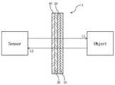
적층체(1)는 특정한 색상 및 광택을 나타내면서, 전파를 투과시킬 수 있다. 따라서 적층체(1)는 차량용 센서 커버로 이용될 수 있다. 도 5에는 센서에서 나오는 전파(L1)가 대상(Object)에 도달하고, 대상으로부터 반사되는 전파(L2)가 센서에 도달하는 모습을 나타내는 개념도가 도시되어 있다. 이하, 적층체(1)에 대하여 그것을 이루는 각 구성요소별로 상술한다.The laminate (1) can transmit radio waves while exhibiting a specific color and luster. Therefore, the
기판(10)은 투명 기판(10)일 수 있다. 이는 증착층(30)이나, 증착층(30) 및 블랙 차폐 코팅층(40)에 반사되는 광의 색상이 그대로 적층체(1)의 외부로 나타나게 하기 위함이다. 또한 이는 증착층(30)이 나타내는 광택을 그대로 적층체(1)의 외부로 나타나게 하기 위함이다. 도 5에서, 사람이 대상 쪽에서 적층체(1)를 바라볼 때, 적층체(1)는 특정한 색상으로 보인다. 이는 대상 쪽에서 조사되어 적층체(1)에 도달하는 광의 일부가, 다시 대상 쪽으로 반사되면서 특정한 색상을 나타내는 것이다. 이는 증착층(30)이나, 증착층(30) 및 블랙 차폐 코팅층(40)에 반사되는 광의 특정한 색상이 그대로 투명 기판(10)을 투과하여 외부로 나타난 것일 수 있다. 구체적으로, 기판(10)은 폴리카보네이트(PC), 폴리메틸메타아크릴레이트(PMMA), 폴리에틸렌테레프탈레이트(PET), 폴리에틸렌나프탈레이트(PEN), 폴리이미드(PI), 사이클로올레핀폴리머(COP), 폴리에테르술폰(PES), 폴리에테르에테르케톤(PEEK), 폴리아릴레이트(PAR), 에이비에스(ABS) 수지, 및 실리콘 수지로 이루어지는 군으로부터 선택되는 하나 이상의 재질로 이루어질 수 있으나, 이에 한정하는 것은 아니다.The
프라이머 코팅층(20)은 아크릴 계열의 수지(주성분), 용제, 및 기타 첨가제가 혼합된 물질로 이루어질 수 있으나, 이에 한정하는 것은 아니다. 그리고 프라이머 코팅층(20)은 도장(painting), 디핑(dipping), 또는 스프레이(spray) 공정으로 형성될 수 있으나, 이에 한정하는 것은 아니다. 또한 프라이머 코팅층(20)은 투명하거나 반투명하다. 이는, 기판(10)의 경우와 마찬가지로, 증착층(30)이나, 증착층(30) 및 블랙 차폐 코팅층(40)에 반사되는 광의 색상이 그대로 적층체(1)의 외부로 나타나게 하기 위함이다. 또한 이는, 기판(10)의 경우와 마찬가지로, 증착층(30)이 나타내는 광택을 그대로 적층체(1)의 외부로 나타나게 하기 위함이다. 또한 프라이머 코팅층(20)은 접착력이 있어, 기판(10) 및 증착층(30)의 접착을 돕는다.The
블랙 차폐 코팅층(40)은 아크릴 계열의 수지(주성분), 흑색 안료, 용제, 및 기타 첨가제가 혼합된 물질로 이루어질 수 있으나, 이에 한정하는 것은 아니다. 그리고 블랙 차폐 코팅층(40)은 도장(painting), 디핑(dipping), 또는 스프레이(spray) 공정으로 형성될 수 있으나, 이에 한정하는 것은 아니다. 또한 블랙 차폐 코팅층(40)은 흑색이다. 이는, 적층체(1)가 차량용 센서 커버로 이용되는 경우, 차량 내부의 부품들이 외부에서 보이지 않는 것이 바람직하기 때문이다. 또한 블랙 차폐 코팅층(40)의 색상은 외부에 보여지는 적층체(1)의 색상과도 관련이 있다. 블랙 차폐 코팅층(40)의 색상이 그대로 외부에 나타나, 적층체(1)가 흑색을 나타낼 수도 있다. 그러나 증착층(30)을 이루는 물질들, 증착층(30)의 두께 등이 변화되어 적층체(1)가 밝은 색상을 나타낼 수도 있다.The black
증착층(30)은 1개 이상의 층이 소정의 증착 방법에 의해 증착되어 형성된다. 증착 방법은 열 증착(thermal evaporation), 전자빔 증착(electron beam evaporation), 스퍼터링(sputtering), 열 CVD(thermal Chemical Vapor Deposition), 플라즈마 CVD(Plasma Enhanced Chemical Vapor Deposition, PECVD), MOCVD(Metal Organic Chemical Vapor Deposition), 및 무전해 도금 중 하나 이상의 방법일 수 있으나, 이에 한정하는 것은 아니다.The
증착층(30)은 저마늄(Ge)층(320)을 포함한다. 저마늄층(320)은 저마늄 또는 저마늄 합금으로 이루어진다. 저마늄은 광택을 나타내고, 전파를 투과시킬 수 있다. 저마늄 합금도 광택을 나타내고, 전파를 투과시킬 수 있다. 저마늄 합금은 저마늄 외에 1개 이상의 원소를 포함하여 이루어진다. 1개 이상의 원소는 주기율표의 3B족 내지 5A족에 속하는 원소일 수 있다. 더욱 구체적으로, 1개 이상의 원소는 금(Au), 은(Ag), 붕소(B), 알루미늄(Al), 갈륨(Ga), 인듐(In), 주석(Sn), 및 탈륨(Tl)으로 이루어지는 군으로부터 선택되는 원소일 수 있다. 저마늄 합금에 있어, 저마늄의 함량은 50 내지 99wt%를 제안하고, 나머지 성분의 함량은 1 내지 50wt%를 제안한다. 저마늄 함량이 50wt% 미만이거나, 나머지 성분 함량이 50wt%를 초과하면, 저마늄층(320)에 의해 나타나는 광택과 금속 질감이 원하는 정도보다 떨어질 수 있다. 저마늄 함량이 99wt%를 초과하거나, 나머지 성분의 함량이 1wt% 미만이면, 저마늄층(320)의 목표 성능(예를 들어, 강도)이 제대로 발휘되지 않을 수 있다.The
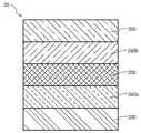
증착층(30)은 저마늄층(320) 외에 다양한 층들을 포함할 수 있다. 예를 들어, 증착층(30)은 저마늄층(320) 및 세라믹층(310)을 포함할 수 있다(도 6 참조). 세라믹층(310)은 세라믹으로 이루어진다. 세라믹층(310)은 적층체(1)의 색상 및 밝기를 조절하는 제1기능, 저마늄층(320)을 외부의 충격으로부터 보호하는 제2기능, 기판(10)(또는 프라이머 코팅층(20))과 저마늄층(320)의 결합력을 향상하는 제3기능 등을 구비할 수 있다. 제1기능을 발휘하기 위해, 세라믹층(310)은 1개 이상의 고굴절률층(311) 및 1개 이상의 저굴절률층(312)을 포함할 수 있다. 고굴절률층(311)은 굴절률이 1.7 내지 2.6일 수 있고, 산화물, 탄화물, 및 질화물로 이루어지는 군으로부터 선택되는 1개 이상의 물질로 이루어질 수 있다. 저굴절률층(312)은 굴절률이 1.4 이상 1.7 미만일 수 있고, 산화물, 탄화물, 및 질화물로 이루어지는 군으로부터 선택되는 1개 이상의 물질로 이루어질 수 있다. 더욱 구체적으로, 고굴절률층(311)은 이산화 타이타늄(TiO2)으로 이루어지고, 저굴절률층(312)은 이산화 규소(SiO2)로 이루어질 수 있다. 고굴절률층(311)의 굴절률과 저굴절률층(312)의 굴절률의 구분 기준은 적층체(1)의 색상 및 밝기를 용이하게 조절하기 위해 정해진 것이다. 다시 말해, 일단 고굴절률층(311)의 굴절률 및 저굴절률층(312)의 굴절률이 정해지면, 세라믹층(310)의 층 수, 세라믹층(310)의 두께, 저마늄층(320)의 두께 등이 조절됨으로써, 적층체(1)의 색상 및 밝기가 조절될 수 있다. 도 6에는 저마늄층(320) 및 세라믹층(310)을 포함하는 증착층(30)의 예시를 나타내는 모식도가 도시되어 있다. 도 6에서, 증착층(30)은 제1고굴절률층(311a), 저마늄층(320), 저굴절률층(312), 및 제2고굴절률층(311b)이 순서대로 증착되어 형성된다. 도 6에서, 제1고굴절률층(311a) 및 저굴절률층(312) 사이에 저마늄층(320)이 위치되므로, 제1고굴절률층(311a) 및 저굴절률층(312)은 상기 제2기능을 발휘한다고 할 수 있다. 또한 도 6에서, 제1고굴절률층(311a) 및 저마늄층(320) 간에는 부착력이 작용하므로, 제1고굴절률층(311a)은 상기 제3기능을 발휘한다고 할 수 있다.The
또 다른 예로, 증착층(30)은 유기물층(330), 아연화합물층(340), 및 저마늄층(320)을 포함할 수 있다(도 7 참조). 유기물층(330)은 유기물로 이루어진다. 구체적으로, 유기물층(330)은 GlipoxanTM으로 이루어질 수 있다. 한편 저마늄층(320)은 수분에 접촉될 경우 산화되기 쉽다. 이는 적층체(1)의 내수성 및 내습성이 좋지 않다는 의미이다. 그러나 적층체(1)가 유기물층(330)을 포함할 경우, 유기물층(330)이 적층체(1)의 내수성 및 내습성을 향상할 수 있다. 아연화합물층(340)은 황화 아연(ZnS) 또는 셀레늄화 아연(ZnSe)으로 이루어진다. 아연화합물층(340)도 적층체(1)의 내수성 및 내습성을 향상하는 기능을 한다. 특히 아연화합물층(340)이 두 층(제1아연화합물층(340a) 및 제2아연화합물층(340b))으로 이루어지고, 두 층 사이에 저마늄층(320)이 위치될 경우, 아연화합물층(340)은 저마늄층(320)을 외부의 충격으로부터 보호하면서 적층체(1)의 내수성 및 내습성을 향상할 수 있다. 또한 아연화합물층(340)이 두 층으로 이루어질 경우, 증착층(30)은 유기물층(330), 제1아연화합물층(340a), 저마늄층(320), 및 제2아연화합물층(340b)이 순서대로 증착되어 형성될 수 있다.As another example, the
또 다른 예로, 증착층(30)은 유기물층(330), 아연화합물층(340), 저마늄층(320), 및 산화크로뮴(CrOx)층(350)을 포함할 수 있다(도 7 참조). 유기물층(330) 및 아연화합물층(340)에 대한 내용은 전술한 바와 같다. 산화크로뮴층(350)은 산화크로뮴으로 이루어진다. 산화크로뮴층(350)은 증착층(30)의 최상층에 증착되어 증착층(30) 전체를 보호한다. 특히 산화크로뮴층(350)이 저마늄층(320)에 수분이 침투하는 것을 방지할 수 있다. 또한 적층체(1)가 블랙 차폐 코팅층(40)을 포함할 경우, 산화크로뮴층(350) 및 블랙 차폐 코팅층(40) 간에는 부착력이 작용한다. 따라서 산화크로뮴층(350)은 증착층(30)과 블랙 차폐 코팅층(40)의 결합력을 향상하는 기능도 한다. 도 7에는 유기물층(330), 아연화합물층(340), 저마늄층(320), 및 산화크로뮴층(350)을 포함하는 증착층(30)의 예시를 나타내는 모식도가 도시되어 있다. 도 7에서, 증착층(30)은 유기물층(330), 제1아연화합물층(340a), 저마늄층(320), 제2아연화합물층(340b), 및 산화크로뮴층(350)이 순서대로 증착되어 형성된다. 도 7에서, 유기물층(330)의 두께는 50 내지 400Å인 것이 바람직하다. 유기물층(330)의 두께가 50Å 미만이면, 유기물층(330)의 내수성 및 내습성 향상 기능이 제대로 발휘되지 않을 수 있다. 유기물층(330)의 두께가 400Å을 초과하면, 저마늄층(320)에 의해 나타나는 광택과 금속 질감이 손상될 수 있다. 또한 이 경우, 적층체(1)의 전파 투과율이 낮을 수도 있다. 도 7에서, 제1아연화합물층(340a)의 두께는 100 내지 600Å인 것이 바람직하다. 제1아연화합물층(340a)의 두께가 100Å 미만이면, 제1아연화합물층(340a)의 내수성 및 내습성 향상 기능이 제대로 발휘되지 않을 수 있다. 또한 이 경우, 제1아연화합물층(340a)이 저마늄층(320)을 외부의 충격으로부터 제대로 보호하지 못할 수 있다. 제1아연화합물층(340a)의 두께가 600Å을 초과하면, 적층체(1)의 전파 투과율이 낮을 수 있다. 도 7에서, 저마늄층(320)의 두께는 150 내지 800Å인 것이 바람직하다. 저마늄층(320)의 두께가 150Å 미만이면, 여러 가지 환경적인 요인에 의해 저마늄층(320)의 박리가 쉽게 일어날 수 있다. 저마늄층(320)의 두께가 800Å을 초과하면, 적층체(1)의 전파 투과율이 낮을 수 있다. 도 7에서, 제2아연화합물층(340b)의 두께는 100 내지 600Å인 것이 바람직하다. 제2아연화합물층(340b)의 두께가 100Å 미만이면, 제2아연화합물층(340b)의 내수성 및 내습성 향상 기능이 제대로 발휘되지 않을 수 있다. 또한 이 경우, 제2아연화합물층(340b)이 저마늄층(320)을 외부의 충격으로부터 제대로 보호하지 못할 수 있다. 제2아연화합물층(340b)의 두께가 600Å을 초과하면, 적층체(1)의 전파 투과율이 낮을 수 있다. 도 7에서, 산화크로뮴층(350)의 두께는 50 내지 400Å인 것이 바람직하다. 산화크로뮴층(350)의 두께가 50Å 미만이면, 산화크로뮴층(350)의 증착층(30) 전체 보호 기능이 약할 수 있다. 산화크로뮴층(350)의 두께가 400Å을 초과하면, 적층체(1)의 전파 투과율이 낮을 수 있다. 투명 기판(10) 상에, 지금까지 상술한 두께 조건을 동시에 만족하는 증착층(30)(도 7에 도시된 증착층(30))이 형성됨으로써 제조되는 적층체(1)는, 흑색(black)을 나타낸다. 흑색의 적층체(1)는 프론트 그릴 및/또는 엠블럼과 어우러질 수 있다.As another example, the
또 다른 예로, 증착층(30)은 세라믹층(310), 유기물층(330), 아연화합물층(340), 저마늄층(320), 및 산화크로뮴층(350)을 포함할 수 있다(도 8 참조). 유기물층(330), 아연화합물층(340), 및 산화크로뮴층(350)에 대한 내용은 전술한 바와 같다. 세라믹층(310)은 세라믹으로 이루어진다. 세라믹층(310)은 증착층(30)의 최하층에 증착되어, 적층체(1)의 색상 및 밝기를 조절한다. 이를 위해, 세라믹층(310)은 1개 이상의 고굴절률층(311) 및 1개 이상의 저굴절률층(312)을 포함할 수 있고, 상기 고굴절률층(311) 및 상기 저굴절률층(312)은 교번적으로 증착될 수 있다. 고굴절률층(311)은 굴절률이 1.7 내지 2.6일 수 있고, 산화물, 탄화물, 및 질화물로 이루어지는 군으로부터 선택되는 1개 이상의 물질로 이루어질 수 있다. 저굴절률층(312)은 굴절률이 1.4 이상 1.7 미만일 수 있고, 산화물, 탄화물, 및 질화물로 이루어지는 군으로부터 선택되는 1개 이상의 물질로 이루어질 수 있다. 더욱 구체적으로, 고굴절률층(311)은 Ti3O5로 이루어지고, 저굴절률층(312)은 이산화 규소로 이루어질 수 있다. 고굴절률층(311)의 굴절률과 저굴절률층(312)의 굴절률의 구분 기준은 적층체(1)의 색상 및 밝기를 용이하게 조절하기 위해 정해진 것이다. 다시 말해, 일단 고굴절률층(311)의 굴절률 및 저굴절률층(312)의 굴절률이 정해지면, 세라믹층(310)의 층 수, 세라믹층(310)의 두께, 저마늄층(320)의 두께 등이 조절됨으로써, 적층체(1)의 색상 및 밝기가 조절될 수 있다. 도 8에는 세라믹층(310), 유기물층(330), 아연화합물층(340), 저마늄층(320), 및 산화크로뮴층(350)을 포함하는 증착층(30)의 예시를 나타내는 모식도가 도시되어 있다. 도 8에서, 증착층(30)은 제1고굴절률층(311a), 제1저굴절률층(312a), 제2고굴절률층(311b), 제2저굴절률층(312b), 유기물층(330), 제1아연화합물층(340a), 저마늄층(320), 제2아연화합물층(340b), 및 산화크로뮴층(350)이 순서대로 증착되어 형성된다. 도 8에서, 유기물층(330)의 두께, 제1아연화합물층(340a)의 두께, 저마늄층(320)의 두께, 제2아연화합물층(340b)의 두께, 및 산화크로뮴층(350)의 두께에 대한 내용은 전술한 바와 같다. 도 8에서, 제1고굴절률층(311a)의 두께는 50 내지 400Å이고, 제1저굴절률층(312a)의 두께는 150 내지 800Å이고, 제2고굴절률층(311b)의 두께는 175 내지 900Å이며, 제2저굴절률층(312b)의 두께는 225 내지 1100Å인 것이 바람직하다. 투명 기판(10) 상에, 지금까지 상술한 두께 조건을 만족하는 증착층(30)(도 8에 도시된 증착층(30))이 형성됨으로써 제조되는 적층체(1)는, 은색(silver)을 나타낸다. 즉, 도 7에 도시된 증착층(30)에, 도 8에 도시된 바와 같이, 세라믹층(310)이 부가됨으로써 적층체(1)의 색상이 흑색에서 은색으로 바뀐 것이다. 은색의 적층체(1)는 프론트 그릴 및/또는 엠블럼과 어우러질 수 있다.As another example, the
[실시예 1 - 흑색 적층체(1)의 제조][Example 1 - Production of black laminate (1)] [
사출성형된 폴리카보네이트 기판(10)을 준비하였다. 기판(10)의 상면을 아크릴 수지를 주성분으로 하는 슬러리로 도장함으로써, 프라이머 코팅층(20)을 형성하였다.An injection molded
프라이머 코팅층(20)이 형성된 기판(10)을 진공 챔버 내의 하부에 장착하고, 진공 챔버 내의 진공도가 7×10⁻⁶Torr가 되도록 배기하였다. 진공 챔버 내에 설치된 MFC(Mass Flow Controller)를 통하여 모노머(Monomer) 상태의 GlipoxanTM을 진공 챔버 내부에 120sccm으로 공급하였다. 그리고 진공 챔버 내에 설치된 플라즈마(Plasma) 발생장치의 전극판에 3000W의 전력(Power)을 인가하였다. 그 결과, 폴리머(Polymer) 상태의 GlipoxanTM이 프라이머 코팅층(20)의 상면에 증착됨으로써, 유기물층(330)이 증착되었다. 이는, 진공 챔버 내부에서, 플라즈마 발생장치에 의한 전기장 내에서 모노머 상태의 GlipoxanTM이 플라즈마 상태로 되었다가, 플라즈마 상태의 물질들이 중합되어 폴리머 상태의 GlipoxanTM이 되는 반응(Plasma polymerization)이 주로 일어난 것이다.Mounting the
프라이머 코팅층(20) 및 유기물층(330)이 형성된 기판(10)을 진공 챔버 내의 상부에 장착하고, 황화 아연 약품을 진공 챔버 내에 설치된 도가니에 주입하였다. 진공 챔버 내의 진공도가 1×10⁻⁵Torr가 되도록 배기하였다. 그리고 진공 챔버 내에 설치된 전자총(Electron beam gun)에 7.5kV의 전압(50 내지 450mA의 전류)을 공급하여, 전자빔(Electron beam)을 황화 아연 약품에 조사하였다. 그 결과, 유기물층(330)의 상면에 황화 아연이 증착됨으로써, 제1아연화합물층(340a)이 증착되었다. 이는, 전자빔의 에너지에 의해 황화 아연이 증발됨으로써, 황화 아연이 유기물층(330)의 상면에 증착된 것이다. 이와 같은 전자빔 증착 방법으로, 제1아연화합물층(340a)의 상면에, 저마늄층(320), 제2아연화합물층(340b), 및 산화크로뮴층(350)을 순서대로 증착하였다. 저마늄층(320)에는 저마늄이 이용되었다. 제2아연화합물층(340b)에는 황화 아연이 이용되었다. 그리고 산화크로뮴층(350)에는 Cr2O3가 이용되었다.The
산화크로뮴층(350)까지 증착된 적층체(1)를 진공 챔버로부터 취출한 다음, 그것을 아크릴 수지를 주성분으로 하고 흑색 안료가 첨가된 슬러리로 도장함으로써, 블랙 차폐 코팅층(40)을 형성하였다.The
즉, 기판(10)-프라이머 코팅층(20)-유기물층(330)-제1아연화합물층(340a)-저마늄층(320)-제2아연화합물층(340b)-산화크로뮴층(350)-블랙 차폐 코팅층(40)으로 이루어지는 적층체(1)를 제조하였다(도 4 및 도 7 참조). 유기물층(330)의 두께는 150Å이었다. 제1아연화합물층(340a)의 두께는 250Å이었다. 저마늄층(320)의 두께는 350Å이었다. 제2아연화합물층(340b)의 두께는 250Å이었다. 그리고 산화크로뮴층(350)의 두께는 150Å이었다.That is, the
[실시예 2 - 실시예 1의 적층체(1)에 세라믹층(310)을 추가하여 은색 적층체(1) 제조][Example 2 - Production of Silver Laminate (1) by Adding Ceramic Layer (310) to Laminate (1) of Example 1]
사출성형된 폴리카보네이트 기판(10)을 준비하였다. 기판(10)의 상면을 아크릴 수지를 주성분으로 하는 슬러리로 도장함으로써, 프라이머 코팅층(20)을 형성하였다.An injection molded
프라이머 코팅층(20)이 형성된 기판(10)을 진공 챔버 내의 상부에 장착하고, Ti3O5 약품을 진공 챔버 내에 설치된 도가니에 주입하였다. 진공 챔버 내의 진공도가 1×10⁻⁵Torr로 되도록 배기하였다. 그리고 진공 챔버 내에 설치된 전자총에 7.5kV의 전압(50 내지 450mA의 전류)을 공급하여, 전자빔을 Ti3O5 약품에 조사하였다. 그 결과, 프라이머 코팅층(20)의 상면에 Ti3O5가 증착됨으로써, 제1고굴절률층(311a)이 증착되었다. 이는, 전자빔의 에너지에 의해 Ti3O5가 증발됨으로써, Ti3O5가 프라이머 코팅층(20)의 상면에 증착된 것이다. 이와 같은 전자빔 증착 방법으로, 제1고굴절률층(311a)의 상면에, 제1저굴절률층(312a), 제2고굴절률층(311b), 및 제2저굴절률층(312b)을 순서대로 증착하였다. 제1저굴절률층(312a) 및 제2저굴절률층(312b)에는 이산화 규소가 이용되었다. 그리고 제2고굴절률층(311b)에는 Ti3O5가 이용되었다.The
프라이머 코팅층(20) 및 세라믹층(310)이 형성된 기판(10)을 진공 챔버 내의 하부에 장착하고, 진공 챔버 내의 진공도가 7×10⁻⁶Torr가 되도록 배기하였다. 진공 챔버 내에 설치된 MFC를 통하여 모노머 상태의 GlipoxanTM을 진공 챔버 내부에 120sccm으로 공급하였다. 그리고 진공 챔버 내에 설치된 플라즈마 발생장치의 전극판에 3000W의 전력을 인가하였다. 그 결과, 폴리머 상태의 GlipoxanTM이 제2저굴절률층(312b)의 상면에 증착됨으로써, 유기물층(330)이 증착되었다. 이는, 진공 챔버 내부에서, Plasma polymerization이 주로 일어난 것이다.Equipped with a
이후로는, 실시예 1에서의 층들과 동일한 층들을 실시예 1에서의 방법과 동일한 방법으로 형성하였다. 즉, 기판(10)-프라이머 코팅층(20)-제1고굴절률층(311a)-제1저굴절률층(312a)-제2고굴절률층(311b)-제2저굴절률층(312b)-유기물층(330)-제1아연화합물층(340a)-저마늄층(320)-제2아연화합물층(340b)-산화크로뮴층(350)-블랙 차폐 코팅층(40)으로 이루어지는 적층체(1)를 제조하였다(도 4 및 도 8 참조). 제1고굴절률층(311a)의 두께는 150Å이었다. 제1저굴절률층(312a)의 두께는 350Å이었다. 제2고굴절률층(311b)의 두께는 400Å이었다. 제2저굴절률층(312b)의 두께는 500Å이었다. 그리고 나머지 층들의 두께는, 이에 대응되는, 실시예 1에서의 층들의 두께와 동일했다.Thereafter, the same layers as the layers in Example 1 were formed in the same manner as the method in Example 1. That is, the
[비교예 1 - 실시예 1의 적층체(1)에서 유기물층(330), 아연화합물층(340), 및 산화크로뮴층(350) 제외]Comparative Example 1 Except for the
사출성형된 폴리카보네이트 기판(10)을 준비하였다. 기판(10)의 상면을 아크릴 수지를 주성분으로 하는 슬러리로 도장함으로써, 프라이머 코팅층(20)을 형성하였다.An injection molded
프라이머 코팅층(20)이 형성된 기판(10)을 진공 챔버 내의 상부에 장착하고, 저마늄 시편을 진공 챔버 내에 설치된 도가니에 투입하였다. 진공 챔버 내의 진공도가 1×10⁻⁵Torr로 되도록 배기하였다. 그리고 진공 챔버 내에 설치된 전자총에 7.5kV의 전압(50 내지 450mA의 전류)을 공급하여, 전자빔을 저마늄 시편에 조사하였다. 그 결과, 프라이머 코팅층(20)의 상면에 저마늄이 증착됨으로써, 저마늄층(320)이 증착되었다. 이는, 전자빔의 에너지에 의해 저마늄이 증발됨으로써, 저마늄이 프라이머 코팅층(20)의 상면에 증착된 것이다.The
저마늄층(320)까지 증착된 적층체(1)를 진공 챔버로부터 취출한 다음, 그것을 아크릴 수지를 주성분으로 하고 흑색 안료가 첨가된 슬러리로 도장함으로써, 블랙 차폐 코팅층(40)을 형성하였다.The
즉, 기판(10)-프라이머 코팅층(20)-저마늄층(320)-블랙 차폐 코팅층(40)으로 이루어지는 적층체(1)를 제조하였다. 저마늄층(320)의 두께는 350Å이었다.That is, a
[비교예 2 - 실시예 1의 적층체(1)에서 유기물층(330) 및 산화크로뮴층(350) 제외][Comparative Example 2-Except for the
사출성형된 폴리카보네이트 기판(10)을 준비하였다. 기판(10)의 상면을 아크릴 수지를 주성분으로 하는 슬러리로 도장함으로써, 프라이머 코팅층(20)을 형성하였다.An injection molded
프라이머 코팅층(20)이 형성된 기판(10)을 진공 챔버 내의 상부에 장착하고, 황화 아연 약품을 진공 챔버 내에 설치된 도가니에 주입하였다. 진공 챔버 내의 진공도가 1×10⁻⁵Torr로 되도록 배기하였다. 그리고 진공 챔버 내에 설치된 전자총에 7.5kV의 전압(50 내지 450mA의 전류)을 공급하여, 전자빔을 황화 아연 약품에 조사하였다. 그 결과, 프라이머 코팅층(20)의 상면에 황화 아연이 증착됨으로써, 제1아연화합물층(340a)이 증착되었다. 이와 같은 전자빔 증착의 방법으로, 제1아연화합물층(340a)의 상면에, 저마늄층(320) 및 제2아연화합물층(340b)을 순서대로 증착하였다. 저마늄층(320)에는 저마늄이 이용되었다. 그리고 제2아연화합물층(340b)에는 황화 아연이 이용되었다.The
제2아연화합물층(340b)까지 증착된 적층체(1)를 진공 챔버로부터 취출한 다음, 그것을 아크릴 수지를 주성분으로 하고 흑색 안료가 첨가된 슬러리로 도장함으로써, 블랙 차폐 코팅층(40)을 형성하였다.The
즉, 기판(10)-프라이머 코팅층(20)-제1아연화합물층(340a)-저마늄층(320)-제2아연화합물층(340b)-블랙 차폐 코팅층(40)으로 이루어지는 적층체(1)를 제조하였다. 제1아연화합물층(340a)의 두께는 250Å이었다. 저마늄층(320)의 두께는 350Å이었다. 그리고 제2아연화합물층(340b)의 두께는 250Å이었다.That is, the
[비교예 3 - 실시예 1의 적층체(1)에서 산화크로뮴층(350) 제외][Comparative Example 3-Except for the
사출성형된 폴리카보네이트 기판(10)을 준비하였다. 기판(10)의 상면을 아크릴 수지를 주성분으로 하는 슬러리로 도장함으로써, 프라이머 코팅층(20)을 형성하였다.An injection molded
프라이머 코팅층(20)이 형성된 기판(10)을 진공 챔버 내의 하부에 장착하고, 진공 챔버 내의 진공도가 7×10⁻⁶Torr가 되도록 배기하였다. 진공 챔버 내에 설치된 MFC를 통하여 모노머 상태의 GlipoxanTM을 진공 챔버 내부에 120sccm으로 공급하였다. 그리고 진공 챔버 내에 설치된 플라즈마 발생장치의 전극판에 3000W의 전력(Power)을 인가하였다. 그 결과, 폴리머 상태의 GlipoxanTM이 프라이머 코팅층(20)의 상면에 증착됨으로써, 유기물층(330)이 증착되었다. 이는, 진공 챔버 내부에서, Plasma polymerization이 주로 일어난 것이다.Mounting the
프라이머 코팅층(20) 및 유기물층(330)이 형성된 기판(10)을 진공 챔버 내의 상부에 장착하고, 황화 아연 약품을 진공 챔버 내에 설치된 도가니에 주입하였다. 진공 챔버 내의 진공도가 1×10⁻⁵Torr가 되도록 배기하였다. 그리고 진공 챔버 내에 설치된 전자총에 7.5kV의 전압(50 내지 450mA의 전류)을 공급하여, 전자빔을 황화 아연 약품에 조사하였다. 그 결과, 유기물층(330)의 상면에 황화 아연이 증착됨으로써, 제1아연화합물층(340a)이 증착되었다. 이는, 전자빔의 에너지에 의해 황화 아연이 증발됨으로써, 황화 아연이 유기물층(330)의 상면에 증착된 것이다. 이와 같은 전자빔 증착 방법으로, 제1아연화합물층(340a)의 상면에, 저마늄층(320) 및 제2아연화합물층(340b)을 순서대로 증착하였다. 저마늄층(320)에는 저마늄이 이용되었다. 그리고 제2아연화합물층(340b)에는 황화 아연이 이용되었다.The
제2아연화합물층(340b)까지 증착된 적층체(1)를 진공 챔버로부터 취출한 다음, 그것을 아크릴 수지를 주성분으로 하고 흑색 안료가 첨가된 슬러리로 도장함으로써, 블랙 차폐 코팅층(40)을 형성하였다.The
즉, 기판(10)-프라이머 코팅층(20)-유기물층(330)-제1아연화합물층(340a)-저마늄층(320)-제2아연화합물층(340b)-블랙 차폐 코팅층(40)으로 이루어지는 적층체(1)를 제조하였다. 유기물층(330)의 두께는 150Å이었다. 제1아연화합물층(340a)의 두께는 250Å이었다. 저마늄층(320)의 두께는 350Å이었다. 그리고 제2아연화합물층(340b)의 두께는 250Å이었다.That is, the
[비교예 4 - 실시예 2의 적층체(1)에서 유기물층(330), 아연화합물층(340), 및 산화크로뮴층(350) 제외]Comparative Example 4 Except for the
기판(10)-프라이머 코팅층(20)-제1고굴절률층(311a)-제1저굴절률층(312a)-제2고굴절률층(311b)-제2저굴절률층(312b)으로 이루어지는 적층체(1)를 제조하였다. 이 적층체(1)에는 실시예 2에서의 물질들과 동일한 물질 및 실시예 2에서의 방법과 동일한 방법이 이용되었다.Layered structure comprising a
프라이머 코팅층(20) 및 세라믹층(310)이 형성된 기판(10)을 진공 챔버 내의 상부에 장착하고, 저마늄 시편을 진공 챔버 내에 설치된 도가니에 투입하였다. 진공 챔버 내의 진공도가 1×10⁻⁵Torr로 되도록 배기하였다. 그리고 진공 챔버 내에 설치된 전자총에 7.5kV의 전압(50 내지 450mA의 전류)을 공급하여, 전자빔을 저마늄 시편에 조사하였다. 그 결과, 제2저굴절률층(312b)의 상면에 저마늄이 증착됨으로써, 저마늄층(320)이 증착되었다. 이는, 전자빔의 에너지에 의해 저마늄이 증발됨으로써, 저마늄이 제2저굴절률층(312b)의 상면에 증착된 것이다.The
저마늄층(320)까지 증착된 적층체(1)를 진공 챔버로부터 취출한 다음, 그것을 아크릴 수지를 주성분으로 하고 흑색 안료가 첨가된 슬러리로 도장함으로써, 블랙 차폐 코팅층(40)을 형성하였다.The
즉, 기판(10)-프라이머 코팅층(20)-제1고굴절률층(311a)-제1저굴절률층(312a)-제2고굴절률층(311b)-제2저굴절률층(312b)-저마늄층(320)-블랙 차폐 코팅층(40)으로 이루어지는 적층체(1)를 제조하였다. 저마늄층(320)의 두께는 350Å이었다.That is, the
[비교예 5 - 실시예 2의 적층체(1)에서 유기물층(330) 및 산화크로뮴층(350) 제외][Comparative Example 5-Except for the
기판(10)-프라이머 코팅층(20)-제1고굴절률층(311a)-제1저굴절률층(312a)-제2고굴절률층(311b)-제2저굴절률층(312b)으로 이루어지는 적층체(1)를 제조하였다. 이 적층체(1)에는 실시예 2에서의 물질들과 동일한 물질 및 실시예 2에서의 방법과 동일한 방법이 이용되었다.Layered structure comprising a
프라이머 코팅층(20) 및 세라믹층(310)이 형성된 기판(10)을 진공 챔버 내의 상부에 장착하고, 황화 아연 약품을 진공 챔버 내에 설치된 도가니에 주입하였다. 진공 챔버 내의 진공도가 1×10⁻⁵Torr가 되도록 배기하였다. 그리고 진공 챔버 내에 설치된 전자총에 7.5kV의 전압(50 내지 450mA의 전류)을 공급하여, 전자빔을 황화 아연 약품에 조사하였다. 그 결과, 제2저굴절률층(312b)의 상면에 황화 아연이 증착됨으로써, 제1아연화합물층(340a)이 증착되었다. 이와 같은 전자빔 증착 방법으로, 제1아연화합물층(340a)의 상면에, 저마늄층(320) 및 제2아연화합물층(340b)을 순서대로 증착하였다. 저마늄층(320)에는 저마늄이 이용되었다. 그리고 제2아연화합물층(340b)에는 황화 아연이 이용되었다.The
제2아연화합물층(340b)까지 증착된 적층체(1)를 진공 챔버로부터 취출한 다음, 그것을 아크릴 수지를 주성분으로 하고 흑색 안료가 첨가된 슬러리로 도장함으로써, 블랙 차폐 코팅층(40)을 형성하였다.The
즉, 기판(10)-프라이머 코팅층(20)-제1고굴절률층(311a)-제1저굴절률층(312a)-제2고굴절률층(311b)-제2저굴절률층(312b)-제1아연화합물층(340a)-저마늄층(320)-제2아연화합물층(340b)-블랙 차폐 코팅층(40)으로 이루어지는 적층체(1)를 제조하였다. 제1아연화합물층(340a)의 두께는 250Å이었다. 저마늄층(320)의 두께는 350Å이었다. 그리고 제2아연화합물층(340b)의 두께는 250Å이었다.That is, the
[비교예 6 - 실시예 2의 적층체(1)에서 산화크로뮴층(350) 제외][Comparative Example 6-Except for the
기판(10)-프라이머 코팅층(20)-제1고굴절률층(311a)-제1저굴절률층(312a)-제2고굴절률층(311b)-제2저굴절률층(312b)으로 이루어지는 적층체(1)를 제조하였다. 이 적층체(1)에는 실시예 2에서의 물질들과 동일한 물질 및 실시예 2에서의 방법과 동일한 방법이 이용되었다.Layered structure comprising a
프라이머 코팅층(20) 및 세라믹층(310)이 형성된 기판(10)을 진공 챔버 내의 하부에 장착하고, 진공 챔버 내의 진공도가 7×10⁻⁶Torr가 되도록 배기하였다. 진공 챔버 내에 설치된 MFC를 통하여 모노머 상태의 GlipoxanTM을 진공 챔버 내부에 120sccm으로 공급하였다. 그리고 진공 챔버 내에 설치된 플라즈마 발생장치의 전극판에 3000W의 전력(Power)을 인가하였다. 그 결과, 폴리머 상태의 GlipoxanTM이 제2저굴절률층(312b)의 상면에 증착됨으로써, 유기물층(330)이 증착되었다. 이는, 진공 챔버 내부에서, Plasma polymerization이 주로 일어난 것이다.Equipped with a
프라이머 코팅층(20), 세라믹층(310), 및 유기물층(330)이 형성된 기판(10)을 진공 챔버 내의 상부에 장착하고, 황화 아연 약품을 진공 챔버 내에 설치된 도가니에 주입하였다. 진공 챔버 내의 진공도가 1×10⁻⁵Torr가 되도록 배기하였다. 그리고 진공 챔버 내에 설치된 전자총에 7.5kV의 전압(50 내지 450mA의 전류)을 공급하여, 전자빔을 황화 아연 약품에 조사하였다. 그 결과, 유기물층(330)의 상면에 황화 아연이 증착됨으로써, 제1아연화합물층(340a)이 증착되었다. 이는, 전자빔의 에너지에 의해 황화 아연이 증발됨으로써, 황화 아연이 유기물층(330)의 상면에 증착된 것이다. 이와 같은 전자빔 증착 방법으로, 제1아연화합물층(340a)의 상면에, 저마늄층(320) 및 제2아연화합물층(340b)을 순서대로 증착하였다. 저마늄층(320)에는 저마늄이 이용되었다. 그리고 제2아연화합물층(340b)에는 황화 아연이 이용되었다.The
제2아연화합물층(340b)까지 증착된 적층체(1)를 진공 챔버로부터 취출한 다음, 그것을 아크릴 수지를 주성분으로 하고 흑색 안료가 첨가된 슬러리로 도장함으로써, 블랙 차폐 코팅층(40)을 형성하였다.The
즉, 기판(10)-프라이머 코팅층(20)-제1고굴절률층(311a)-제1저굴절률층(312a)-제2고굴절률층(311b)-제2저굴절률층(312b)-유기물층(330)-제1아연화합물층(340a)-저마늄층(320)-제2아연화합물층(340b)-블랙 차폐 코팅층(40)으로 이루어지는 적층체(1)를 제조하였다. 유기물층(330)의 두께는 150Å이었다. 제1아연화합물층(340a)의 두께는 250Å이었다. 저마늄층(320)의 두께는 350Å이었다. 그리고 제2아연화합물층(340b)의 두께는 250Å이었다.That is, the
[실험예 1 - 반사율 측정][Experimental Example 1 - Reflectance Measurement]
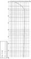
실시예 1 및 실시예 2에서 제조된 적층체(1)들에 대하여 반사율을 측정하였다(Hitachi spectrophotometer U-3010). 실시예 1에서 제조된 적층체(1)에 대한 반사율 측정 결과는 도 9에 도시되어 있다. 그리고 실시예 2에서 제조된 적층체(1)에 대한 반사율 측정 결과는 도 10에 도시되어 있다.The reflectance was measured (Hitachi spectrophotometer U-3010) on the layered product (1) prepared in Example 1 and Example 2. The reflectance measurement results for the
도 9에서, 적층체(1)의 반사율 그래프(Ge Black)는 흑색 기준 그래프(Black Reference)와 유사하게 나타나므로, 실시예 1에서 제조된 적층체(1)는 흑색이라는 것을 알 수 있다. 또한 도 9에서, 적층체(1)의 반사율 그래프는, 종래에 저마늄이 아닌 인듐(In) 또는 주석(Sn)이 이용된 적층체(1)보다 높은 반사율을 나타낸다. 이는 실시예 1에서 제조된 적층체(1)가 광택이 있어 우수한 금속 질감을 나타낸다는 것을 의미한다.9, the reflectance graph (Ge Black) of the
도 10에서, 적층체(1)의 반사율 그래프(Ge Silver)는 은색 기준 그래프(Silver Reference)와 유사하게 나타나므로, 실시예 2에서 제조된 적층체(1)는 은색이라는 것을 알 수 있다. 또한 도 10에서, 적층체(1)의 반사율 그래프는, 종래에 저마늄이 아닌 인듐(In) 또는 주석(Sn)이 이용된 적층체(1)보다 높은 반사율을 나타낸다. 이는 실시예 2에서 제조된 적층체(1)가 광택이 있어 우수한 금속 질감을 나타낸다는 것을 의미한다.In FIG. 10, the reflectance graph (Ge Silver) of the
즉, 실시예 1에서 제조된 적층체(1)는 흑색 및 광택을 나타내고, 실시예 2에서 제조된 적층체(1)는 은색 및 광택을 나타낸다는 것을 확인하였다. 물론 이러한 결과를 육안으로도 확인하였다.That is, it was confirmed that the layered product (1) produced in Example 1 exhibited blackness and luster, and the layered product (1) produced in Example 2 exhibited silver and luster. Of course, these results were visually confirmed.
[실험예 2 - 전파 감쇠율 측정][Experimental Example 2 - Measurement of the propagation attenuation rate]
실시예 1 및 실시예 2에서 제조된 적층체(1)들에 대하여 전파 감쇠율을 측정하였다(SM5899). 그 결과는 다음 표 1과 같다.The propagation damping ratios were measured for the laminates (1) prepared in Examples 1 and 2 (SM5899). The results are shown in Table 1 below.

표 1에 나타난 바와 같이, 실시예 1에서 제조된 적층체(1)를 투과한 전파는 -0.62dB만큼 변화하였고, 실시예 2에서 제조된 적층체(1)를 투과한 전파는 -0.66dB만큼 변화하였다. 즉, 실시예 1에서 제조된 적층체(1)를 투과한 전파와 실시예 2에서 제조된 적층체(1)를 투과한 전파는, 둘 다 10% 미만으로 감쇠하여, 실시예 1 및 실시예 2에서 제조된 적층체(1)들의 전파 투과율이 만족스러운 수준임을 확인하였다.As shown in Table 1, the radio wave transmitted through the
[실험예 3 - 내수성 실험][Experimental Example 3 - Water resistance test]
실시예 1, 실시예 2, 비교예 1 내지 비교예 6에서 제조된 적층체(1)들에 대하여 내수성 실험을 하였다. 상기 적층체(1)들을 40℃의 물에 240시간 동안 침적시킨 후, 상기 적층체(1)들을 물에서 꺼냈다. 상기 적층체(1)들에 공기를 분사하여 수분을 제거한 후, 실온에서 1시간 동안 방치하였다. 그 후, 상기 적층체(1)들을 육안으로 확인하였고, 그 결과는 다음 표 2와 같다.The laminate (1) prepared in Examples 1, 2 and Comparative Examples 1 to 6 was subjected to a water resistance test. After the laminate (1) was immersed in water at 40 캜 for 240 hours, the laminate (1) was taken out of the water. Air was blown into the stacked bodies (1) to remove moisture, and then left to stand at room temperature for 1 hour. Thereafter, the above-mentioned layered product (1) was visually confirmed, and the results are shown in Table 2 below.

표 2에 나타난 바와 같이, 실시예 1 및 실시예 2를 제외하고, 다른 모든 경우에 산화가 발생하였다. 이는 적층체(1)의 우수한 내수성을 위해, 유기물층(330), 아연화합물층(340), 및 산화크로뮴층(350)이 모두 필요함을 의미한다.As shown in Table 2, except for Example 1 and Example 2, oxidation occurred in all other cases. This means that both the
비교예 3에서 제조된 적층체(1)보다 비교예 2에서 제조된 적층체(1)의 산화가 더 심하게 발생했다. 비교예 2에서 제조된 적층체(1)보다 비교예 1에서 제조된 적층체(1)의 산화가 더 심하게 발생했다. 참고로, 비교예 2에서 제조된 적층체(1)에 대한 내수성 실험 결과 이미지는 도 11에 도시되어 있고, 비교예 1에서 제조된 적층체(1)에 대한 내수성 실험 결과 이미지는 도 12에 도시되어 있다. 비교예 6에서 제조된 적층체(1)보다 비교예 5에서 제조된 적층체(1)의 산화가 더 심하게 발생했다. 그리고 비교예 5에서 제조된 적층체(1)보다 비교예 4에서 제조된 적층체(1)의 산화가 더 심하게 발생했다.Oxidation of the layered product (1) produced in Comparative Example 2 was more severe than in the layered product (1) produced in Comparative Example 3. Oxidation of the layered product (1) produced in Comparative Example 1 was more severe than in the layered product (1) produced in Comparative Example 2. 11, the image of the result of the water resistance test on the
실시예 1에서 제조된 적층체(1)에 대한 내수성 실험 후에, 이 적층체(1)에 대하여 반사율을 측정한 결과가 도 13에 도시되어 있다. 그리고 실시예 2에서 제조된 적층체(1)에 대한 내수성 실험 후에, 이 적층체(1)에 대하여 반사율을 측정한 결과가 도 14에 도시되어 있다. 도 13에 도시된 바와 같이, 실시예 1에서 제조된 적층체(1)의 내수성 실험 후 반사율 그래프(After Test)는, 내수성 실험 전 반사율 그래프(Before Test)와 거의 동일하다. 그리고 도 14에 도시된 바와 같이, 실시예 2에서 제조된 적층체(1)의 내수성 실험 후 반사율 그래프(After Test)는, 내수성 실험 전 반사율 그래프(Before Test)와 거의 동일하다. 이는 실시예 1 및 실시예 2에서 제조된 적층체(1)들이 수분에 접촉한 후에도, 그것들의 색상이나 광택이 거의 변하지 않음을 의미한다.FIG. 13 shows the result of measuring the reflectance with respect to this
결론적으로, 실시예 1 및 실시예 2에서 제조된 적층체(1)들은 (i) 특정한 색상 및 광택을 나타내면서도, (ii) 전파를 투과시킬 수 있고, (iii) 내수성이 우수함을 확인하였다.As a result, it was confirmed that the laminate (1) produced in Examples 1 and 2 exhibited (i) a specific color and luster, (ii) the ability to transmit radio waves, and (iii) excellent water resistance.
본 발명을 첨부된 도면과 함께 설명하였으나, 이는 본 발명의 요지를 포함하는 다양한 실시 형태 중의 하나의 실시예에 불과하며, 당업계에서 통상의 지식을 가진 자가 용이하게 실시할 수 있도록 하는 데에 그 목적이 있는 것으로, 본 발명은 상기 설명된 실시예에만 국한되는 것이 아님은 명확하다. 따라서, 본 발명의 보호범위는 하기의 청구범위에 의해 해석되어야 하며, 본 발명의 요지를 벗어나지 않는 범위 내에서의 변경, 치환, 대체 등에 의해 그와 동등한 범위 내에 있는 모든 기술 사상은 본 발명의 권리범위에 포함될 것이다. 또한, 도면의 일부 구성은 구성을 보다 명확하게 설명하기 위한 것으로 실제보다 과장되거나 축소되어 제공된 것임을 명확히 한다.While the present invention has been particularly shown and described with reference to exemplary embodiments thereof, it should be understood that various changes and modifications will be apparent to those skilled in the art. Obviously, the invention is not limited to the embodiments described above. Accordingly, the scope of protection of the present invention should be construed according to the following claims, and all technical ideas which fall within the scope of equivalence by alteration, substitution, substitution, Range. In addition, it should be clarified that some configurations of the drawings are intended to explain the configuration more clearly and are provided in an exaggerated or reduced size than the actual configuration.
1 : 적층체
10 : 기판
20 : 프라이머 코팅층
30 : 증착층
310 : 세라믹층
311 : 고굴절률층
311a : 제1고굴절률층
311b : 제2고굴절률층
312 : 저굴절률층
312a : 제1저굴절률층
312b : 제2저굴절률층
320 : 저마늄층
330 : 유기물층
340 : 아연화합물층
340a : 제1아연화합물층
340b : 제2아연화합물층
350 : 산화크로뮴층
40 : 블랙 차폐 코팅층1:
10: substrate
20: primer coating layer
30: Deposition layer
310: Ceramic layer
311: high refractive index layer
311a: a first high refractive index layer
311b: a second high refractive index layer
312: low refractive index layer
312a: a first low refractive index layer
312b: second low refractive index layer
320: the lowermanium layer
330: organic layer
340: zinc compound layer
340a: the first zinc compound layer
340b: Second zinc compound layer
350: chromium oxide layer
40: Black shielding coating layer
Claims (30)
Translated fromKorean상기 기판의 상부에 형성되며, 빛이 통과하도록 투명 또는 반투명한 재질로 이루어지는 프라이머 코팅층;
상기 프라이머 코팅층의 상부에 형성되며 빛을 반사시키고 광택을 나타내는 증착층; 및
상기 증착층의 상부에 형성되어 빛을 차단하고 흑색을 나타내는 블랙 차폐 코팅층;을 포함하여 이루어지고,
상기 증착층은 광택을 나타내고 전파를 투과시킬 수 있는 저마늄층 및 서로 상이한 굴절률을 가지며 상기 저마늄층을 상부와 하부에서 감싸도록 형성되는 세라믹층을 포함하며,
상기 세라믹층은, 1.7 내지 2.6의 굴절률을 가지도록 이산화 타이타늄(TiO2) 또는 오산화 타이타늄(Ti3O5)으로 이루어지는 하나 이상의 고굴절률층 및 1.4 내지 1.7의 굴절률을 가지도록 이산화 규소(SiO2)로 이루어지는 하나 이상의 저굴절률층이 상기 저마늄층을 사이에 두고 상호 교번적으로 증착되어 형성되며,
상기 고굴절률층 및 저굴절률층의 굴절률에 대응한 상기 세라믹층 및 저마늄층의 두께에 따라 색상 및 밝기가 조절되고, 상기 증착층을 투과하는 76.5GHz 주파수 영역의 전파가 10% 미만의 감쇠율을 가지는 것을 특징으로 하는 색상 조절 및 전파 투과 가능한 차량용 센서 커버 적층체.
A substrate made of a transparent material to allow light to pass therethrough;
A primer coating layer formed on the substrate, the primer coating layer being made of transparent or semitransparent material to allow light to pass therethrough;
A deposition layer formed on the primer coating layer and reflecting and reflecting light; And
And a black shielding coating layer formed on the deposition layer to block light and display a black color,
Wherein the deposition layer comprises a germanium layer that is lustrous and capable of transmitting radio waves, and a ceramic layer that has different refractive indices and is formed to surround the germanium layer at the top and bottom,
Wherein the ceramic layer comprises one or more high refractive index layers made of titanium dioxide (TiO2 ) or titanium pentoxide (Ti3 O5 ) having a refractive index of 1.7 to 2.6 and silicon dioxide (SiO2 ) having a refractive index of 1.4 to 1.7. Wherein the low-refractive-index layer is formed by alternately depositing the low-
The color and brightness are controlled according to the thickness of the ceramic layer and the lowermanium layer corresponding to the refractive indexes of the high refractive index layer and the low refractive index layer and the electromagnetic wave in the 76.5 GHz frequency region transmitting through the vapor deposition layer has a decay rate of less than 10% Wherein the sensor cover layer is formed of a transparent material.
상기 저마늄층은 순수 저마늄(Ge)으로 이루어지는 것을 특징으로 하는 색상 조절 및 전파 투과 가능한 차량용 센서 커버 적층체.
The method according to claim 1,
Wherein the germanium layer is made of pure germanium (Ge).
상기 저마늄층은 저마늄 합금으로 이루어지며,
저마늄 50 내지 99wt% 및
주기율표의 3B족 내지 5A족에 속하는 금(Au), 은(Ag), 붕소(B), 알루미늄(Al), 갈륨(Ga), 인듐(In), 주석(Sn) 및 탈륨(Tl)으로 이루어지는 군으로부터 선택되는 하나 이상의 원소 1 내지 50wt% 를 포함하도록 이루어져, 금속 광택을 유지하는 동시에 강도를 향상시키는 것을 특징으로 하는 색상 조절 및 전파 투과 가능한 차량용 센서 커버 적층체.
The method according to claim 1,
The germanium layer is made of a germanium alloy,
50 to 99 wt% of germanium and
(Al), gallium (Ga), indium (In), tin (Sn) and thallium (Tl) belonging to Group 3B to Group 5A of the periodic table And 1 to 50 wt% of at least one element selected from the group consisting of a metal and a metal, to improve the strength while maintaining the metallic luster.
상기 저마늄층의 두께는 150 내지 800Å으로 형성되어, 상기 저마늄층의 박리를 방지하는 동시에 전파 투과율을 향상시키도록 이루어지는 것을 특징으로 하는 색상 조절 및 전파 투과 가능한 차량용 센서 커버 적층체.
The method according to claim 1,
Wherein the thickness of the germanium layer is in the range of 150 to 800 angstroms so as to prevent peeling of the germanium layer and to improve the radio wave transmittance.
폴리카보네이트(PC), 폴리메틸메타아크릴레이트(PMMA), 폴리에틸렌테레프탈레이트(PET), 폴리에틸렌나프탈레이트(PEN), 폴리이미드(PI), 사이클로올레핀폴리머(COP), 폴리에테르술폰(PES), 폴리에테르에테르케톤(PEEK), 폴리아릴레이트(PAR), 에이비에스(ABS) 수지, 및 실리콘 수지로 이루어지는 군으로부터 선택되는 하나 이상의 재질로 이루어지는 것을 특징으로 하는 색상 조절 및 전파 투과 가능한 차량용 센서 커버 적층체.
The substrate processing apparatus according to claim 1,
(PC), polymethylmethacrylate (PMMA), polyethylene terephthalate (PET), polyethylene naphthalate (PEN), polyimide (PI), cycloolefin polymer (COP), polyether sulfone Characterized in that it comprises at least one material selected from the group consisting of ether ether ketone (PEEK), polyarylate (PAR), epoxy resin (ABS), and silicone resin. .
상기 기판의 상부에 형성되며, 빛이 통과하도록 투명 또는 반투명한 재질로 이루어지는 프라이머 코팅층;
상기 프라이머 코팅층의 상부에 형성되며 빛을 반사시키고 광택을 나타내는 증착층; 및
상기 증착층의 상부에 형성되어 빛을 차단하고 흑색을 나타내는 블랙 차폐 코팅층;을 포함하여 이루어지고,
상기 증착층은,
광택을 나타내고 전파를 투과시킬 수 있는 저마늄층;
상기 저마늄층의 일측면에 증착되며 황화 아연(ZnS) 또는 셀레늄화 아연(ZnSe)으로 이루어지는 제1아연화합물층;
상기 저마늄층의 타측면에 증착되며 황화 아연(ZnS) 또는 셀레늄화 아연(ZnSe)으로 이루어지는 제2아연화합물층;
상기 제1아연화합물층의 일면 중 상기 저마늄층이 위치하는 면의 반대면에 위치하여 상기 저마늄층의 내수성 및 내습성을 향상시키는 유기물층; 및
상기 제2아연화합물층의 일면 중 상기 저마늄층이 위치하는 면의 반대면에 위치하여 상기 증착층을 보호하고 상기 저마늄층으로 수분이 침투하는 것을 방지하며 상기 증착층과 상기 블랙 차폐 코팅층의 결합력을 향상시키는 산화크로뮴층; 을 포함하도록 이루어져, 상기 증착층에 의하여 흑색 계열의 색상을 나타내는 것을 특징으로 하는 색상 조절 및 전파 투과 가능한 차량용 센서 커버 적층체.
A substrate made of a transparent material to allow light to pass therethrough;
A primer coating layer formed on the substrate, the primer coating layer being made of transparent or semitransparent material to allow light to pass therethrough;
A deposition layer formed on the primer coating layer and reflecting and reflecting light; And
And a black shielding coating layer formed on the deposition layer to block light and display a black color,
The vapor-
A germanium layer which is lustrous and can transmit radio waves;
A first zinc compound layer deposited on one side of the germanium layer and made of zinc sulfide (ZnS) or zinc selenide (ZnSe);
A second zinc compound layer deposited on the other side of the germanium layer and made of zinc sulfide (ZnS) or zinc selenide (ZnSe);
An organic material layer disposed on a surface of the first zinc compound layer opposite to the surface on which the germanium layer is disposed to improve the water resistance and moisture resistance of the germanium layer; And
The second zinc compound layer is located on the opposite surface of the one surface of the second zinc compound layer opposite to the surface on which the germanium layer is disposed to protect the vapor deposition layer and prevent moisture from penetrating into the germanium layer and improve the bonding force between the vapor deposition layer and the black shielding coating layer A chromium oxide layer; Wherein the color of the black color is changed by the vapor deposition layer.
상기 유기물층의 두께는 50 내지 400Å으로 형성되어, 상기 저마늄층에 의한 광택과 금속 질감을 유지하는 동시에 내수성 및 내습성을 향상시키는 것을 특징으로 하는 색상 조절 및 전파 투과 가능한 차량용 센서 커버 적층체.
The method according to claim 6,
Wherein the organic material layer is formed to a thickness of 50 to 400 ANGSTROM to improve the water resistance and moisture resistance while maintaining the luster and metal texture by the germanium layer.
상기 저마늄층의 두께는 150 내지 800Å으로 형성되어, 상기 저마늄층의 박리를 방지하는 동시에 전파 투과율을 향상시키도록 이루어지는 것을 특징으로 하는 색상 조절 및 전파 투과 가능한 차량용 센서 커버 적층체.
The method according to claim 6,
Wherein the thickness of the germanium layer is in the range of 150 to 800 angstroms so as to prevent peeling of the germanium layer and to improve the radio wave transmittance.
상기 제1아연화합물층 및 제2아연화합물층은 그 두께가 100 내지 600Å으로 형성되며, 상기 저마늄층을 사이에 두고 상기 저마늄층의 양 측면을 감싸도록 이루어져, 상기 저마늄층을 외부의 충격으로부터 보호하면서 내수성 및 내습성을 향상시키고, 상기 증착층을 투과하는 76.5GHz 주파수 영역의 전파가 10% 미만의 감쇠율을 가지도록 전파 투과율이 유지되는 것을 특징으로 하는 색상 조절 및 전파 투과 가능한 차량용 센서 커버 적층체.
The method according to claim 6,
The first zinc compound layer and the second zinc compound layer are formed to have a thickness of 100 to 600 angstroms. The first zinc compound layer and the second zinc compound layer are formed so as to surround both sides of the germanium layer with the germanium layer interposed therebetween. And the moisture permeability is improved, and the radio wave transmittance is maintained so that the wave in the 76.5 GHz frequency region transmitted through the vapor deposition layer has a decay rate of less than 10%.
상기 산화크로뮴층의 두께는 50 내지 400Å으로 형성되어 상기 증착층을 보호하는 동시에 전파 투과율을 향상시키도록 이루어지는 것을 특징으로 하는 색상 조절 및 전파 투과 가능한 차량용 센서 커버 적층체.
The method according to claim 6,
Wherein the thickness of the chromium oxide layer is in the range of 50 to 400 angstroms so as to protect the vapor deposition layer and to improve the radio wave transmittance.
상기 기판의 상부에 형성되며, 빛이 통과하도록 투명 또는 반투명한 재질로 이루어지는 프라이머 코팅층;
상기 프라이머 코팅층의 상부에 형성되며 빛을 반사시키고 광택을 나타내는 증착층; 및
상기 증착층의 상부에 형성되어 빛을 차단하고 흑색을 나타내는 블랙 차폐 코팅층;을 포함하여 이루어지고,
상기 증착층은,
광택을 나타내고 전파를 투과시킬 수 있는 저마늄층;
상기 저마늄층의 일측면에 증착되며 황화 아연(ZnS) 또는 셀레늄화 아연(ZnSe)으로 이루어지는 제1아연화합물층;
상기 저마늄층의 타측면에 증착되며 황화 아연(ZnS) 또는 셀레늄화 아연(ZnSe)으로 이루어지는 제2아연화합물층;
상기 제1아연화합물층의 일면 중 상기 저마늄층이 위치하는 면의 반대면에 위치하여 상기 저마늄층의 내수성 및 내습성을 향상시키는 유기물층;
상기 제2아연화합물층의 일면 중 상기 저마늄층이 위치하는 면의 반대면에 위치하여 상기 증착층을 보호하고 상기 저마늄층으로 수분이 침투하는 것을 방지하며 상기 증착층과 상기 블랙 차폐 코팅층의 결합력을 향상시키는 산화크로뮴층; 및
상기 유기물층의 일면 중 상기 저마늄층이 위치하는 면의 반대면에 위치하는 세라믹층을 포함하며,
상기 세라믹층은,
1.7 내지 2.6의 굴절률을 가지도록 이산화 타이타늄(TiO2) 또는 오산화 타이타늄(Ti3O5)으로 이루어지는 하나 이상의 고굴절률층 및 1.4 내지 1.7의 굴절률을 가지도록 이산화 규소(SiO2)로 이루어지는 하나 이상의 저굴절률층이 상호 교번적으로 증착되어 형성되며,
상기 고굴절률층 및 저굴절률층의 굴절률에 대응한 상기 세라믹층 및 저마늄층의 두께에 따라 색상 및 밝기가 조절되고, 상기 세라믹층을 포함하는 상기 증착층에 의하여 은색 계열의 색상을 나타내며, 상기 증착층을 투과하는 76.5GHz 주파수 영역의 전파가 10% 미만의 감쇠율을 가지는 것을 특징으로 하는 색상 조절 및 전파 투과 가능한 차량용 센서 커버 적층체.
A substrate made of a transparent material to allow light to pass therethrough;
A primer coating layer formed on the substrate, the primer coating layer being made of transparent or semitransparent material to allow light to pass therethrough;
A deposition layer formed on the primer coating layer and reflecting and reflecting light; And
And a black shielding coating layer formed on the deposition layer to block light and display a black color,
The vapor-
A germanium layer which is lustrous and can transmit radio waves;
A first zinc compound layer deposited on one side of the germanium layer and made of zinc sulfide (ZnS) or zinc selenide (ZnSe);
A second zinc compound layer deposited on the other side of the germanium layer and made of zinc sulfide (ZnS) or zinc selenide (ZnSe);
An organic material layer disposed on a surface of the first zinc compound layer opposite to the surface on which the germanium layer is disposed to improve the water resistance and moisture resistance of the germanium layer;
The second zinc compound layer is located on the opposite surface of the one surface of the second zinc compound layer opposite to the surface on which the germanium layer is disposed to protect the vapor deposition layer and prevent moisture from penetrating into the germanium layer and improve the bonding force between the vapor deposition layer and the black shielding coating layer A chromium oxide layer; And
And a ceramic layer on one surface of the organic material layer, the ceramic layer being positioned on a surface opposite to a surface on which the germanium layer is disposed,
In the ceramic layer,
At least one high refractive index layer made of titanium dioxide (TiO2 ) or titanium pentoxide (Ti3 O5 ) having a refractive index of 1.7 to 2.6 and at least one high refractive index layer made of silicon dioxide (SiO2 ) having a refractive index of 1.4 to 1.7 Refractive index layers are alternately deposited and formed,
The color and brightness of the ceramic layer and the lowermanium layer corresponding to the refractive indexes of the high refractive index layer and the low refractive index layer are adjusted and the color of the silver layer is represented by the vapor deposition layer including the ceramic layer, Wherein the propagation in the 76.5 GHz frequency region transmitting through the layer has a decay rate of less than 10%.
상기 세라믹층은,
제1고굴절률층, 제1저굴절률층, 제2고굴절률층 및 제2저굴절률층이 순서대로 증착되어 형성되는 것을 특징으로 하는 색상 조절 및 전파 투과 가능한 차량용 센서 커버 적층체.
12. The method of claim 11,
In the ceramic layer,
Wherein the first high refractive index layer, the first low refractive index layer, the second high refractive index layer, and the second low refractive index layer are sequentially deposited and formed.
상기 제1고굴절률층의 두께는 50 내지 400Å, 상기 제1저굴절률층의 두께는 150 내지 800Å, 상기 제2고굴절률층의 두께는 175 내지 900Å, 상기 제2저굴절률층의 두께는 225 내지 1100Å으로 이루어져, 상기 증착층에 의하여 은색의 색상을 나타내도록 이루어지는 것을 특징으로 하는 색상 조절 및 전파 투과 가능한 차량용 센서 커버 적층체.
13. The method of claim 12,
Wherein the thickness of the first high refractive index layer is 50 to 400 angstroms, the thickness of the first low refractive index layer is 150 to 800 angstroms, the thickness of the second high refractive index layer is 175 to 900 angstroms, Wherein the transparent cover layer is formed to have a silver color by the vapor deposition layer.
상기 유기물층의 두께는 50 내지 400Å으로 형성되어, 상기 저마늄층에 의한 광택과 금속 질감을 유지하는 동시에 내수성 및 내습성을 향상시키는 것을 특징으로 하는 색상 조절 및 전파 투과 가능한 차량용 센서 커버 적층체.
12. The method of claim 11,
Wherein the organic material layer is formed to a thickness of 50 to 400 ANGSTROM to improve the water resistance and moisture resistance while maintaining the luster and metal texture by the germanium layer.
상기 저마늄층의 두께는 150 내지 800Å으로 형성되어, 상기 저마늄층의 박리를 방지하는 동시에 전파 투과율을 향상시키도록 이루어지는 것을 특징으로 하는 색상 조절 및 전파 투과 가능한 차량용 센서 커버 적층체.
12. The method of claim 11,
Wherein the thickness of the germanium layer is in the range of 150 to 800 angstroms so as to prevent peeling of the germanium layer and to improve the radio wave transmittance.
상기 제1아연화합물층 및 제2아연화합물층은 그 두께가 100 내지 600Å으로 형성되며, 상기 저마늄층을 사이에 두고 상기 저마늄층의 양 측면을 감싸도록 이루어져, 상기 저마늄층을 외부의 충격으로부터 보호하면서 내수성 및 내습성을 향상시키고, 전파 투과율이 유지되는 것을 특징으로 하는 색상 조절 및 전파 투과 가능한 차량용 센서 커버 적층체.
12. The method of claim 11,
The first zinc compound layer and the second zinc compound layer are formed to have a thickness of 100 to 600 angstroms. The first zinc compound layer and the second zinc compound layer are formed so as to surround both sides of the germanium layer with the germanium layer interposed therebetween. And moisture resistance, and maintains the radio wave transmittance.
상기 산화크로뮴층의 두께는 50 내지 400Å으로 형성되어 상기 증착층을 보호하는 동시에 전파 투과율을 향상시키도록 이루어지는 것을 특징으로 하는 색상 조절 및 전파 투과 가능한 차량용 센서 커버 적층체.
12. The method of claim 11,
Wherein the thickness of the chromium oxide layer is in the range of 50 to 400 angstroms so as to protect the vapor deposition layer and to improve the radio wave transmittance.
상기 저마늄층은 순수 저마늄(Ge)으로 이루어지는 것을 특징으로 하는 색상 조절 및 전파 투과 가능한 차량용 센서 커버 적층체.
12. The method of claim 11,
Wherein the germanium layer is made of pure germanium (Ge).
상기 저마늄층은 저마늄 합금으로 이루어지며,
저마늄 50 내지 99wt% 및
주기율표의 3B족 내지 5A족에 속하는 금(Au), 은(Ag), 붕소(B), 알루미늄(Al), 갈륨(Ga), 인듐(In), 주석(Sn) 및 탈륨(Tl)으로 이루어지는 군으로부터 선택되는 하나 이상의 원소 1 내지 50wt% 를 포함하도록 이루어져, 금속 광택을 유지하는 동시에 강도를 향상시키는 것을 특징으로 하는 색상 조절 및 전파 투과 가능한 차량용 센서 커버 적층체.
12. The method of claim 11,
The germanium layer is made of a germanium alloy,
50 to 99 wt% of germanium and
(Al), gallium (Ga), indium (In), tin (Sn) and thallium (Tl) belonging to Group 3B to Group 5A of the periodic table And 1 to 50 wt% of at least one element selected from the group consisting of a metal and a metal, to improve the strength while maintaining the metallic luster.
폴리카보네이트(PC), 폴리메틸메타아크릴레이트(PMMA), 폴리에틸렌테레프탈레이트(PET), 폴리에틸렌나프탈레이트(PEN), 폴리이미드(PI), 사이클로올레핀폴리머(COP), 폴리에테르술폰(PES), 폴리에테르에테르케톤(PEEK), 폴리아릴레이트(PAR), 에이비에스(ABS) 수지, 및 실리콘 수지로 이루어지는 군으로부터 선택되는 하나 이상의 재질로 이루어지는 것을 특징으로 하는 색상 조절 및 전파 투과 가능한 차량용 센서 커버 적층체.
12. The method of claim 11,
(PC), polymethylmethacrylate (PMMA), polyethylene terephthalate (PET), polyethylene naphthalate (PEN), polyimide (PI), cycloolefin polymer (COP), polyether sulfone Characterized in that it comprises at least one material selected from the group consisting of ether ether ketone (PEEK), polyarylate (PAR), epoxy resin (ABS), and silicone resin. .
Priority Applications (5)
| Application Number | Priority Date | Filing Date | Title |
|---|---|---|---|
| EP16848860.9AEP3355408B1 (en) | 2015-09-23 | 2016-09-13 | Stacked body |
| US15/763,009US10570500B2 (en) | 2015-09-23 | 2016-09-13 | Sensor cover laminates for vehicle adjusting color and penetrating electronic waves |
| CN201680055648.6ACN108028461B (en) | 2015-09-23 | 2016-09-13 | Laminated body |
| PCT/KR2016/010326WO2017052134A1 (en) | 2015-09-23 | 2016-09-13 | Stacked body |
| ES16848860TES2806277T3 (en) | 2015-09-23 | 2016-09-13 | Stacked body |
Applications Claiming Priority (2)
| Application Number | Priority Date | Filing Date | Title |
|---|---|---|---|
| KR20150134924 | 2015-09-23 | ||
| KR1020150134924 | 2015-09-23 |
Publications (2)
| Publication Number | Publication Date |
|---|---|
| KR20170035773A KR20170035773A (en) | 2017-03-31 |
| KR101869157B1true KR101869157B1 (en) | 2018-06-19 |
Family
ID=58501116
Family Applications (1)
| Application Number | Title | Priority Date | Filing Date |
|---|---|---|---|
| KR1020160109354AActiveKR101869157B1 (en) | 2015-09-23 | 2016-08-26 | Sensor cover laminates for vehicle adjusting color and penetrating electronic waves |
Country Status (5)
| Country | Link |
|---|---|
| US (1) | US10570500B2 (en) |
| EP (1) | EP3355408B1 (en) |
| KR (1) | KR101869157B1 (en) |
| CN (1) | CN108028461B (en) |
| ES (1) | ES2806277T3 (en) |
Cited By (1)
| Publication number | Priority date | Publication date | Assignee | Title |
|---|---|---|---|---|
| KR20240092998A (en)* | 2022-12-15 | 2024-06-24 | 국방과학연구소 | Manufacturing method of junction device using the chalcogenide infrared ray glass having infrared transmitting and sealing characteristic and junction device manufactured thereof |
Families Citing this family (7)
| Publication number | Priority date | Publication date | Assignee | Title |
|---|---|---|---|---|
| JP6677191B2 (en)* | 2017-02-15 | 2020-04-08 | トヨタ自動車株式会社 | Vehicle front structure |
| KR101824090B1 (en)* | 2017-04-07 | 2018-03-15 | 김병삼 | Laminates for a sensor cover |
| KR101810815B1 (en)* | 2017-04-07 | 2017-12-20 | 김병삼 | Manufacturing method of sensor cover penetrating electronic signal having micro crack and laser hole |
| EP3956943A1 (en) | 2019-04-18 | 2022-02-23 | SRG Global, LLC | Stepped radar cover and method of manufacture |
| KR102281990B1 (en)* | 2019-09-09 | 2021-07-28 | (주)아이에이 | Sensor Cover for Smart Cruise Control |
| JP2023521886A (en) | 2020-04-17 | 2023-05-25 | アイデックス ラボラトリーズ インコーポレイテッド | Fluorescence quenching immunoassay |
| CN114086121B (en)* | 2021-11-23 | 2022-11-22 | 北京航空航天大学 | A High Performance Radiative Cooling Inorganic Multilayer Film |
Citations (1)
| Publication number | Priority date | Publication date | Assignee | Title |
|---|---|---|---|---|
| JP2006153976A (en)* | 2004-11-25 | 2006-06-15 | Nippon Shinku Kogaku Kk | Infra-red light transmission filter |
Family Cites Families (17)
| Publication number | Priority date | Publication date | Assignee | Title |
|---|---|---|---|---|
| US5144498A (en)* | 1990-02-14 | 1992-09-01 | Hewlett-Packard Company | Variable wavelength light filter and sensor system |
| CA2089778C (en)* | 1992-05-19 | 1998-08-25 | Leo Joseph Amore | Optimized rf-transparent antenna sunshield membrane |
| JPH07503833A (en)* | 1992-05-19 | 1995-04-20 | マーチン・マリエッタ・コーポレーション | Direct sunlight shielding film for radio frequency antennas |
| JP3614644B2 (en) | 1998-02-27 | 2005-01-26 | 松下電器産業株式会社 | Manufacturing method of laminate |
| DE19844021C2 (en) | 1998-09-25 | 2001-05-10 | Daimler Chrysler Ag | Cladding part located within the beam path of a radar device |
| KR20020091535A (en)* | 2001-05-31 | 2002-12-06 | 주식회사 엔티밸리 | Multilayer interference film |
| JP3940709B2 (en)* | 2003-07-01 | 2007-07-04 | 株式会社東芝 | Phase change optical recording medium |
| US7291223B2 (en) | 2003-09-24 | 2007-11-06 | Nitto Denko Corporation | Epitaxial organic layered structure and method for making |
| JP2005249773A (en)* | 2004-02-02 | 2005-09-15 | Toyota Motor Corp | Molded product for beam path of radar equipment |
| JP2006264593A (en)* | 2005-03-25 | 2006-10-05 | Toyota Motor Corp | Brightening molded parts for radar device beam path |
| CN101233434A (en)* | 2005-07-29 | 2008-07-30 | 旭硝子株式会社 | Laminate for reflective film |
| US8861087B2 (en)* | 2007-08-12 | 2014-10-14 | Toyota Motor Corporation | Multi-layer photonic structures having omni-directional reflectivity and coatings incorporating the same |
| JP2009092913A (en)* | 2007-10-09 | 2009-04-30 | Toppan Printing Co Ltd | Optical thin film laminate |
| JP5401132B2 (en)* | 2009-01-20 | 2014-01-29 | 信越ポリマー株式会社 | Radio wave transmitting decorative member and manufacturing method thereof |
| US9114760B2 (en) | 2010-11-15 | 2015-08-25 | Zanini Auto Grup, Sa | Decorative radome for automotive vehicular applications |
| JPWO2013151136A1 (en)* | 2012-04-05 | 2015-12-17 | コニカミノルタ株式会社 | Infrared shielding film and infrared shielding body |
| KR102025906B1 (en)* | 2017-12-06 | 2019-11-04 | 삼성전자주식회사 | Antenna module |
- 2016
- 2016-08-26KRKR1020160109354Apatent/KR101869157B1/enactiveActive
- 2016-09-13ESES16848860Tpatent/ES2806277T3/enactiveActive
- 2016-09-13USUS15/763,009patent/US10570500B2/enactiveActive
- 2016-09-13CNCN201680055648.6Apatent/CN108028461B/enactiveActive
- 2016-09-13EPEP16848860.9Apatent/EP3355408B1/enactiveActive
Patent Citations (1)
| Publication number | Priority date | Publication date | Assignee | Title |
|---|---|---|---|---|
| JP2006153976A (en)* | 2004-11-25 | 2006-06-15 | Nippon Shinku Kogaku Kk | Infra-red light transmission filter |
Cited By (2)
| Publication number | Priority date | Publication date | Assignee | Title |
|---|---|---|---|---|
| KR20240092998A (en)* | 2022-12-15 | 2024-06-24 | 국방과학연구소 | Manufacturing method of junction device using the chalcogenide infrared ray glass having infrared transmitting and sealing characteristic and junction device manufactured thereof |
| KR102801776B1 (en) | 2022-12-15 | 2025-04-30 | 국방과학연구소 | Manufacturing method of junction device using the chalcogenide infrared ray glass having infrared transmitting and sealing characteristic and junction device manufactured thereof |
Also Published As
| Publication number | Publication date |
|---|---|
| KR20170035773A (en) | 2017-03-31 |
| US10570500B2 (en) | 2020-02-25 |
| US20180291496A1 (en) | 2018-10-11 |
| ES2806277T8 (en) | 2021-02-24 |
| EP3355408A1 (en) | 2018-08-01 |
| CN108028461A (en) | 2018-05-11 |
| EP3355408B1 (en) | 2020-04-29 |
| ES2806277T3 (en) | 2021-02-17 |
| CN108028461B (en) | 2021-10-26 |
| EP3355408A4 (en) | 2019-04-17 |
Similar Documents
| Publication | Publication Date | Title |
|---|---|---|
| KR101869157B1 (en) | Sensor cover laminates for vehicle adjusting color and penetrating electronic waves | |
| KR102271407B1 (en) | Metallic lustrous member with electromagnetic wave transmissibility, article using the member, and metal thin film | |
| CN106908884B (en) | Radio wave-transparent layer having metallic luster | |
| EP3425730B1 (en) | Radome for vehicles | |
| EP0049083A1 (en) | Laminated film | |
| US7824782B2 (en) | Molded article located in the beam path of radar device, and method of manufacturing the same | |
| JP2004152727A (en) | Transparent conductive film | |
| CN102282288A (en) | Radio wave transparent decorative part and manufacturing method thereof | |
| JP7516707B2 (en) | Radio wave-transmitting metallic glossy member, article using same, and method for manufacturing same | |
| KR102679771B1 (en) | Electromagnetic wave transparent metallic shiny articles, and metallic thin films | |
| CN112020422A (en) | Electromagnetic wave-permeable metallic luster article and decorative member | |
| KR101824090B1 (en) | Laminates for a sensor cover | |
| KR20220040766A (en) | Vehicle sensor cover laminated for easy transmission of radio waves | |
| JP7670684B2 (en) | Electromagnetic wave transparent metallic glossy material | |
| TW202003217A (en) | Electromagnetic wave transmissive metal luster article | |
| CN112004663B (en) | Electromagnetic wave-transparent metallic glossy article and metallic film | |
| WO2017052134A1 (en) | Stacked body | |
| WO2019139122A1 (en) | Radio wave-transmitting lustrous metal member, article using same, and method for producing same | |
| WO2019208494A1 (en) | Electromagnetic wave transmissive metallic luster product and metal thin film | |
| KR102281990B1 (en) | Sensor Cover for Smart Cruise Control | |
| CN112020424A (en) | Electromagnetic wave transmitting metallic luster article | |
| JP7687894B2 (en) | Laminate and decorative member | |
| WO2022004671A1 (en) | Electromagnetic wave-permeable metallic luster member, and decorative member | |
| JP2022102748A (en) | Laminates and decorative members | |
| JP2022102747A (en) | Laminates and decorative members |
Legal Events
| Date | Code | Title | Description |
|---|---|---|---|
| A201 | Request for examination | ||
| PA0109 | Patent application | Patent event code:PA01091R01D Comment text:Patent Application Patent event date:20160826 | |
| PA0201 | Request for examination | ||
| PG1501 | Laying open of application | ||
| E902 | Notification of reason for refusal | ||
| PE0902 | Notice of grounds for rejection | Comment text:Notification of reason for refusal Patent event date:20170726 Patent event code:PE09021S01D | |
| E701 | Decision to grant or registration of patent right | ||
| PE0701 | Decision of registration | Patent event code:PE07011S01D Comment text:Decision to Grant Registration Patent event date:20180316 | |
| GRNT | Written decision to grant | ||
| PR0701 | Registration of establishment | Comment text:Registration of Establishment Patent event date:20180612 Patent event code:PR07011E01D | |
| PR1002 | Payment of registration fee | Payment date:20180612 End annual number:3 Start annual number:1 | |
| PG1601 | Publication of registration | ||
| PR1001 | Payment of annual fee | Payment date:20210609 Start annual number:4 End annual number:4 | |
| PR1001 | Payment of annual fee | Payment date:20220614 Start annual number:5 End annual number:5 | |
| PR1001 | Payment of annual fee | Payment date:20230613 Start annual number:6 End annual number:6 | |
| PR1001 | Payment of annual fee | Payment date:20240610 Start annual number:7 End annual number:7 | |
| PR1001 | Payment of annual fee | Payment date:20250602 Start annual number:8 End annual number:8 |