KR101868704B1 - Capacitive pressure sensor - Google Patents
Capacitive pressure sensorDownload PDFInfo
- Publication number
- KR101868704B1 KR101868704B1KR1020160183234AKR20160183234AKR101868704B1KR 101868704 B1KR101868704 B1KR 101868704B1KR 1020160183234 AKR1020160183234 AKR 1020160183234AKR 20160183234 AKR20160183234 AKR 20160183234AKR 101868704 B1KR101868704 B1KR 101868704B1
- Authority
- KR
- South Korea
- Prior art keywords
- elastic
- electrode
- pressure
- layer
- elastic layer
- Prior art date
- Legal status (The legal status is an assumption and is not a legal conclusion. Google has not performed a legal analysis and makes no representation as to the accuracy of the status listed.)
- Expired - Fee Related
Links
Images


Classifications
- H—ELECTRICITY
- H10—SEMICONDUCTOR DEVICES; ELECTRIC SOLID-STATE DEVICES NOT OTHERWISE PROVIDED FOR
- H10N—ELECTRIC SOLID-STATE DEVICES NOT OTHERWISE PROVIDED FOR
- H10N30/00—Piezoelectric or electrostrictive devices
- H10N30/30—Piezoelectric or electrostrictive devices with mechanical input and electrical output, e.g. functioning as generators or sensors
- H10N30/302—Sensors
- H01L41/1132—
- G—PHYSICS
- G01—MEASURING; TESTING
- G01L—MEASURING FORCE, STRESS, TORQUE, WORK, MECHANICAL POWER, MECHANICAL EFFICIENCY, OR FLUID PRESSURE
- G01L9/00—Measuring steady of quasi-steady pressure of fluid or fluent solid material by electric or magnetic pressure-sensitive elements; Transmitting or indicating the displacement of mechanical pressure-sensitive elements, used to measure the steady or quasi-steady pressure of a fluid or fluent solid material, by electric or magnetic means
- G01L9/0001—Transmitting or indicating the displacement of elastically deformable gauges by electric, electro-mechanical, magnetic or electro-magnetic means
- G01L9/0005—Transmitting or indicating the displacement of elastically deformable gauges by electric, electro-mechanical, magnetic or electro-magnetic means using variations in capacitance
- H01L41/047—
- H01L41/083—
- H01L41/18—
- H—ELECTRICITY
- H10—SEMICONDUCTOR DEVICES; ELECTRIC SOLID-STATE DEVICES NOT OTHERWISE PROVIDED FOR
- H10N—ELECTRIC SOLID-STATE DEVICES NOT OTHERWISE PROVIDED FOR
- H10N30/00—Piezoelectric or electrostrictive devices
- H10N30/50—Piezoelectric or electrostrictive devices having a stacked or multilayer structure
- H—ELECTRICITY
- H10—SEMICONDUCTOR DEVICES; ELECTRIC SOLID-STATE DEVICES NOT OTHERWISE PROVIDED FOR
- H10N—ELECTRIC SOLID-STATE DEVICES NOT OTHERWISE PROVIDED FOR
- H10N30/00—Piezoelectric or electrostrictive devices
- H10N30/80—Constructional details
- H10N30/85—Piezoelectric or electrostrictive active materials
- H—ELECTRICITY
- H10—SEMICONDUCTOR DEVICES; ELECTRIC SOLID-STATE DEVICES NOT OTHERWISE PROVIDED FOR
- H10N—ELECTRIC SOLID-STATE DEVICES NOT OTHERWISE PROVIDED FOR
- H10N30/00—Piezoelectric or electrostrictive devices
- H10N30/80—Constructional details
- H10N30/87—Electrodes or interconnections, e.g. leads or terminals
Landscapes
- Physics & Mathematics (AREA)
- General Physics & Mathematics (AREA)
- Measuring Fluid Pressure (AREA)
Abstract
Translated fromKoreanDescription
Translated fromKorean본 발명의 실시예들은 정전용량형 압력 센서에 관한 것이다. 보다 상세하게는, 외부로부터 가해지는 압력의 크기를 정전 용량 변화를 이용하여 측정할 수 있는 정전용량형 압력 센서에 관한 것이다.Embodiments of the invention relate to capacitive pressure sensors. More particularly, the present invention relates to a capacitive pressure sensor capable of measuring the magnitude of pressure externally applied using a change in capacitance.
일반적으로, 압력 센서는 압력을 감지하는 원리에 따라 압저항형 압력 센서(Piezoresistive pressure sensor), 압전형 압력 센서(Piezoelectric pressure sensor, MOSFET형 압력 센서, 광섬유 압력 센서, 정전용량형 압력 센서(Capacitive pressure sensor) 등이 있다.Generally, a pressure sensor is classified into a piezoresistive pressure sensor, a piezo-electric pressure sensor, a MOSFET-type pressure sensor, a fiber-optic pressure sensor, a capacitive pressure sensor sensor).
정전용량형 압력 센서는 제1 전극, 제1 전극과 마주하게 배치된 제2 전극, 및 제1 전극과 제2 전극 사이에 개재된 유전층을 포함할 수 있다. 외부로부터 가해지는 압력에 의해 제1 전극이 휘어질 경우 제1 전극과 제2 전극 간의 간격이 변한다. 이러한 간격 변화에 의해 압력 센서의 정전용량 값이 변하게 되며, 이를 통해 외부로부터 가해진 압력의 크기가 측정될 수 있다.The capacitive pressure sensor may include a first electrode, a second electrode facing the first electrode, and a dielectric layer interposed between the first electrode and the second electrode. The gap between the first electrode and the second electrode changes when the first electrode is bent by a pressure applied from the outside. The change of the gap causes the capacitance value of the pressure sensor to change, and the magnitude of the pressure externally applied can be measured.
정전용량형 압력 센서에 구비되는 유전층은 압력에 대응하여 압축과 복원이 가능한 탄성 재질로 이루어진다. 유전층은 외부로부터 압력이 가해질 경우 압력에 의해 압축되며, 이에 따라, 제1 전극과 제2 전극 간의 거리가 변경된다. 또한, 유전층은 외부의 압력이 해지될 경우 초기 상태로 복원되며, 이에 따라, 제1 전극과 제2 전극 간의 거리가 압력이 가해지기 전의 거리로 원복된다.The dielectric layer of the capacitance type pressure sensor is made of an elastic material capable of being compressed and restored in response to the pressure. The dielectric layer is compressed by pressure when externally applied pressure, thereby changing the distance between the first electrode and the second electrode. Also, the dielectric layer is restored to the initial state when the external pressure is released, whereby the distance between the first electrode and the second electrode is changed to a distance before the pressure is applied.
특히, 유전층은 내부에 복수의 기공을 구비할 수 있으며, 그 결과, 미세한 압력에 대한 반응도를 높이고 압력 해지시 복원 속도를 높일 수 있다. 그러나 유전층이 외부 압력에 의해 너무 쉽게 눌리기 때문에, 유전층의 두께의 약 60% 내지 약 90% 정도를 압축할 수 있는 압력이 가해질 경우 유전층이 손상되거나 복원력이 저하된다. 이로 인해, 압력 센서의 정전 용량이 급격하게 증가하여 압력 센서의 출력값을 입력받는 IC의 입력 가능 범위를 넘을 수 있고, 유전층이 너무 쉽게 눌리기 때문에 측정 가능한 압력의 최대 세기가 낮아 압력이 높을수록 그 크기를 정확하게 측정하기 어렵다.Particularly, the dielectric layer can have a plurality of pores therein, and as a result, it is possible to increase the degree of response to a minute pressure and increase the recovery speed at the time of pressure release. However, since the dielectric layer is pressed too easily by external pressure, the dielectric layer is damaged or the restoring force is lowered when a pressure capable of compressing about 60% to about 90% of the thickness of the dielectric layer is applied. As a result, the capacitance of the pressure sensor rapidly increases, the output value of the pressure sensor can exceed the input range of the input IC, and the maximum intensity of the measurable pressure is low because the dielectric layer is pressed too easily. It is difficult to accurately measure the size.
이와 같이, 압력 센서의 압력 측정 범위는 유전층에 의해 결정될 수 있으며, 유전층은 외부로부터 가해지는 압력의 크기에 따라 눌림 정도가 달라지기 때문에 유전층의 경도에 따라 측정 가능한 압력의 범위가 달라진다. 즉, 유전층의 경도가 낮을수록 외부 압력에 의해 유전층이 잘 눌리기 때문에, 미세한 압력을 측정하기 쉬우나 최대 압력 임계치가 낮아 압력이 높을수록 세밀하게 측정하기 어려운 문제점이 있다. 반면, 유전층의 경도가 높을수록 유전층이 잘 눌리지 않기 때문에, 측정 가능한 압력의 최대 세기가 높아 압력이 높을수록 세밀하게 측정할 수 있으나 미세한 압력은 측정하기가 어려운 문제점이 있다.As described above, the pressure measuring range of the pressure sensor can be determined by the dielectric layer, and the range of the pressure that can be measured varies depending on the hardness of the dielectric layer, since the degree of pressing varies depending on the magnitude of the pressure applied from the outside. That is, since the dielectric layer is pressed by the external pressure as the hardness of the dielectric layer is lower, it is easy to measure the minute pressure, but the maximum pressure threshold is low. On the other hand, since the dielectric layer is not pressed well as the hardness of the dielectric layer is high, the maximum intensity of the measurable pressure is high, and the higher the pressure, the finer the measurement is, but the minute pressure is difficult to measure.
본 발명의 실시예들은 측정 가능한 압력의 세기를 확장하고 압력을 세밀하게 측정할 수 있는 정전용량형 압력 센서를 제공하는 것이다.Embodiments of the present invention provide a capacitive pressure sensor that can extend the strength of a measurable pressure and accurately measure pressure.
상기 목적을 달성하기 위한 본 발명의 일 실시예들에 따르면, 정전용량형 압력 센서는, 제1 전극과, 상기 제1 전극과 마주하여 배치된 제2 전극과, 상기 제1 전극과 상기 제2 전극 사이에 개재된 유전층을 포함할 수 있다. 상기 유전층은, 상기 제1 및 제2 전극들의 배치 방향과 동일한 방향으로 배치되어 서로 마주하게 구비되며 서로 다른 경도를 갖는 복수의 탄성층을 구비할 수 있다.According to an aspect of the present invention, there is provided a capacitive pressure sensor including a first electrode, a second electrode disposed to face the first electrode, And a dielectric layer interposed between the electrodes. The dielectric layer may include a plurality of elastic layers disposed in the same direction as the arrangement direction of the first and second electrodes and facing each other and having different hardnesses.
본 발명의 실시예들에 따르면, 상기 복수의 탄성층은, 내부에 복수의 기공을 구비하고 시트 형상을 가지며 상기 제1 및 제2 전극들과 마주하여 배치된 제1 탄성층과, 상기 제1 탄성층과 서로 다른 경도를 갖는 복수의 탄성 돌기를 구비하고 상기 제1 탄성층과 상기 제2 전극 사이에 배치된 제2 탄성층을 포함할 수 있다. 여기서, 상기 탄성 돌기들은 상기 제1 및 제2 전극들의 배치 방향에 대해 수직하는 방향으로 서로 이격되어 배치될 수 있다.According to embodiments of the present invention, the plurality of elastic layers may include: a first elastic layer having a plurality of pores therein and having a sheet shape and disposed facing the first and second electrodes; And a second elastic layer having a plurality of elastic protrusions having different hardness from the elastic layer and disposed between the first elastic layer and the second electrode. Here, the elastic protrusions may be spaced apart from each other in a direction perpendicular to the arrangement direction of the first and second electrodes.
본 발명의 실시예들에 따르면, 상기 탄성 돌기들은 상기 제1 탄성층의 경도보다 높은 경도를 가질 수 있다.According to embodiments of the present invention, the elastic protrusions may have a hardness higher than the hardness of the first elastic layer.
본 발명의 실시예들에 따르면, 상기 유전층은, 상기 탄성 돌기들을 사이에 두고 상기 제1 탄성층과 서로 마주하게 배치되며 일면에 상기 탄성 돌기들이 배치된 베이스 필름을 더 포함할 수 있다.According to embodiments of the present invention, the dielectric layer may further include a base film having the elastic protrusions disposed on one surface of the dielectric layer facing the first elastic layer with the elastic protrusions therebetween.
본 발명의 실시예들에 따르면, 상기 탄성 돌기들 각각은 기둥 형상을 가질 수 있다.According to embodiments of the present invention, each of the elastic projections may have a columnar shape.
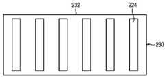
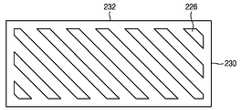
본 발명의 실시예들에 따르면, 상기 탄성 돌기들은 각각 스트라이프 형상을 가지며, 상기 베이스 필름의 일변에 대해 수직 방향 또는 사선 방향으로 배치될 수 있다.According to embodiments of the present invention, the elastic protrusions each have a stripe shape, and may be disposed in a direction perpendicular or oblique to one side of the base film.
본 발명의 실시예들에 따르면, 상기 탄성 돌기들 각각은 상기 베이스 필름과 접하는 부위를 제외한 부위들이 상기 제1 탄성층에 의해 커버될 수 있다.According to the embodiments of the present invention, each of the elastic protrusions may be covered with the first elastic layer at portions other than a portion in contact with the base film.
본 발명의 실시예들에 따르면, 상기 탄성 돌기들은 일면들이 상기 베이스 필름과 접하고, 타면들이 상기 제1 탄성층과 접하며, 상기 탄성 돌기들의 이격 공간은 상기 제2 탄성층의 통기공으로 제공될 수 있다.According to the embodiments of the present invention, the elastic protrusions may contact one surface of the base film, the other surfaces may contact the first elastic layer, and the spacing space of the elastic protrusions may be provided as a vent hole of the second elastic layer .
본 발명의 실시예들에 따르면, 상기 제2 탄성층은 상기 제1 탄성층이 압축될 수 있는 압력 구간 보다 높은 압력 구간에서 압축될 수 있다.According to embodiments of the present invention, the second elastic layer can be compressed in a pressure section higher than a pressure section in which the first elastic layer can be compressed.
상술한 바와 같은 본 발명의 실시예들에 따르면, 압력 센서는 경도가 서로 다른 복수의 탄성층을 구비하는 유전층을 구비함으로써, 유전층의 두께 증가 없이 미세한 압력뿐만 아니라 높은 압력 또한 세밀하고 정확하게 측정할 수 있다. 그 결과, 압력 센서는 측정 가능한 압력 범위를 확장시킬 수 있고 센서 정확도와 품질을 향상시킬 수 있으며 제1 탄성층의 손상을 방지할 수 있다.According to the embodiments of the present invention as described above, since the pressure sensor has the dielectric layer having a plurality of elastic layers having different hardnesses, it is possible to measure not only the fine pressure but also the high pressure, have. As a result, the pressure sensor can expand the measurable pressure range, improve the sensor accuracy and quality, and prevent damage to the first elastic layer.
도 1은 본 발명의 일 실시예에 따른 정전용량형 압력 센서를 설명하기 위한 개략적인 단면도이다.
도 2는 도 1에 도시된 유전층을 설명하기 위한 개략적인 단면도이다.
도 3은 도 2에 도시된 복수의 탄성 돌기를 설명하기 위한 개략적인 평면도이다.
도 4 및 도 5는 도 3에 도시된 탄성 돌기들의 다른 일례를 설명하기 위한 개략적인 평면도들이다.
도 6은 도 2에 도시된 유전층이 외부 압력에 의해 압축된 상태를 설명하기 위한 개략적인 단면도이다.
도 7은 도 2에 도시된 유전층을 형성하는 과정을 설명하기 위한 개략적인 공정 단면도이다.
도 8은 도 2에 도시된 유전층의 다른 일례를 설명하기 위한 개략적인 단면도이다.1 is a schematic cross-sectional view illustrating a capacitive pressure sensor according to an embodiment of the present invention.
2 is a schematic cross-sectional view for explaining the dielectric layer shown in Fig.
Fig. 3 is a schematic plan view for explaining a plurality of elastic projections shown in Fig. 2. Fig.
Figs. 4 and 5 are schematic plan views for explaining another example of the elastic projections shown in Fig.
6 is a schematic cross-sectional view for explaining a state where the dielectric layer shown in FIG. 2 is compressed by external pressure.
FIG. 7 is a schematic process sectional view for explaining the process of forming the dielectric layer shown in FIG. 2. FIG.
8 is a schematic cross-sectional view for explaining another example of the dielectric layer shown in Fig.
이하, 본 발명의 실시예들은 첨부 도면들을 참조하여 상세하게 설명된다. 그러나, 본 발명은 하기에서 설명되는 실시예들에 한정된 바와 같이 구성되어야만 하는 것은 아니며 이와 다른 여러 가지 형태로 구체화될 수 있을 것이다. 하기의 실시예들은 본 발명이 온전히 완성될 수 있도록 하기 위하여 제공된다기보다는 본 발명의 기술 분야에서 숙련된 당업자들에게 본 발명의 범위를 충분히 전달하기 위하여 제공된다.Hereinafter, embodiments of the present invention will be described in detail with reference to the accompanying drawings. However, the present invention should not be construed as limited to the embodiments described below, but may be embodied in various other forms. The following examples are provided so that those skilled in the art can fully understand the scope of the present invention, rather than being provided so as to enable the present invention to be fully completed.
본 발명의 실시예들에서 하나의 요소가 다른 하나의 요소 상에 배치되는 또는 연결되는 것으로 설명되는 경우 상기 요소는 상기 다른 하나의 요소 상에 직접 배치되거나 연결될 수도 있으며, 다른 요소들이 이들 사이에 개재될 수도 있다. 이와 다르게, 하나의 요소가 다른 하나의 요소 상에 직접 배치되거나 연결되는 것으로 설명되는 경우 그들 사이에는 또 다른 요소가 있을 수 없다. 다양한 요소들, 조성들, 영역들, 층들 및/또는 부분들과 같은 다양한 항목들을 설명하기 위하여 제1, 제2, 제3 등의 용어들이 사용될 수 있으나, 상기 항목들은 이들 용어들에 의하여 한정되지는 않을 것이다.In the embodiments of the present invention, when one element is described as being placed on or connected to another element, the element may be disposed or connected directly to the other element, . Alternatively, if one element is described as being placed directly on another element or connected, there can be no other element between them. The terms first, second, third, etc. may be used to describe various items such as various elements, compositions, regions, layers and / or portions, but the items are not limited by these terms .
본 발명의 실시예들에서 사용된 전문 용어는 단지 특정 실시예들을 설명하기 위한 목적으로 사용되는 것이며, 본 발명을 한정하기 위한 것은 아니다. 또한, 달리 한정되지 않는 이상, 기술 및 과학 용어들을 포함하는 모든 용어들은 본 발명의 기술 분야에서 통상적인 지식을 갖는 당업자에게 이해될 수 있는 동일한 의미를 갖는다. 통상적인 사전들에서 한정되는 것들과 같은 상기 용어들은 관련 기술과 본 발명의 설명의 문맥에서 그들의 의미와 일치하는 의미를 갖는 것으로 해석될 것이며, 명확히 한정되지 않는 한 이상적으로 또는 과도하게 외형적인 직감으로 해석되지는 않을 것이다.The terminology used in the embodiments of the present invention is used for the purpose of describing specific embodiments only, and is not intended to be limiting of the present invention. Furthermore, all terms including technical and scientific terms have the same meaning as will be understood by those skilled in the art having ordinary skill in the art, unless otherwise specified. These terms, such as those defined in conventional dictionaries, shall be construed to have meanings consistent with their meanings in the context of the related art and the description of the present invention, and are to be interpreted as being ideally or externally grossly intuitive It will not be interpreted.
본 발명의 실시예들은 본 발명의 이상적인 실시예들의 개략적인 도해들을 참조하여 설명된다. 이에 따라, 상기 도해들의 형상들로부터의 변화들, 예를 들면, 제조 방법들 및/또는 허용 오차들의 변화는 충분히 예상될 수 있는 것들이다. 따라서, 본 발명의 실시예들은 도해로서 설명된 영역들의 특정 형상들에 한정된 바대로 설명되어지는 것은 아니라 형상들에서의 편차를 포함하는 것이며, 도면들에 설명된 요소들은 전적으로 개략적인 것이며 이들의 형상은 요소들의 정확한 형상을 설명하기 위한 것이 아니며 또한 본 발명의 범위를 한정하고자 하는 것도 아니다.Embodiments of the present invention are described with reference to schematic illustrations of ideal embodiments of the present invention. Accordingly, changes from the shapes of the illustrations, e.g., changes in manufacturing methods and / or tolerances, are those that can be reasonably expected. Accordingly, the embodiments of the present invention should not be construed as being limited to the specific shapes of the regions described in the drawings, but include deviations in the shapes, and the elements described in the drawings are entirely schematic and their shapes Is not intended to describe the exact shape of the elements and is not intended to limit the scope of the invention.
도 1은 본 발명의 일 실시예에 따른 정전용량형 압력 센서를 설명하기 위한 개략적인 단면도이다.1 is a schematic cross-sectional view illustrating a capacitive pressure sensor according to an embodiment of the present invention.
도 1을 참조하면, 본 발명의 일 실시예에 따른 정전용량형 압력 센서(100)는 외부로부터 가해지는 압력의 크기를 정전 용량 변화를 이용하여 측정하는 센서로서, 제1 전극(110)과, 상기 제1 전극(110)과 마주하여 배치된 제2 전극(120)과, 상기 제1 및 제2 전극들(110, 120) 사이에 개재된 유전층(201)을 포함할 수 있다.1, a capacitance
구체적으로, 상기 제1 전극(110)은 감지 전극으로 이용될 수 있으며, ITO, 구리, 은 등과 같은 도전성 금속으로 이루어질 수 있다.Specifically, the
상기 제2 전극(120)은 외부로부터 가해지는 압력에 의해 잘 눌리고 원복될 수 있도록 유연한 도전성 재질, 예컨대, ITO와 같은 재질로 이루어질 수 있다.The
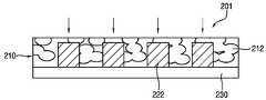
상기 유전층(201)은 탄성 재질로 이루어지며, 상기 제1 전극(110)과 상기 제2 전극(120) 간의 적정 거리를 유지시킨다. 상기 압력 센서(100)는 외부로부터 가해지는 압력에 의해 상기 유전층(201)이 눌림으로써 상기 제1 전극(110)과 상기 제2 전극(120) 간의 거리가 변하며, 그 결과, 상기 압력 센서(100)의 정전 용량이 변한다. 이러한 정전 용량의 변화를 이용하여 상기 외부로부터 가해진 압력의 크기가 측정될 수 있다.The
특히, 상기 유전층(201)은 서로 다른 경도를 갖는 복수의 탄성층(210, 220)을 구비함으로써, 상기 압력 센서(100)가 측정할 수 있는 압력의 세기 범위를 종래 대비 확장할 수 있다.In particular, since the
이하, 도면을 참조하여 본 발명에 따른 상기 유전층(201)에 대해 구체적으로 설명한다.Hereinafter, the
도 2는 도 1에 도시된 유전층을 설명하기 위한 개략적인 단면도이고, 도 3은 도 2에 도시된 복수의 탄성 돌기를 설명하기 위한 개략적인 평면도이다.FIG. 2 is a schematic cross-sectional view for explaining the dielectric layer shown in FIG. 1, and FIG. 3 is a schematic plan view for explaining a plurality of elastic protrusions shown in FIG.
도 1 및 도 2를 참조하면, 본 발명에 따른 상기 유전층(201)은, 상기 제1 및 제2 전극들(110, 120)의 배치 방향과 동일한 방향으로 배치되어 서로 마주하는 상기 복수의 탄성층(210, 220)과, 상기 탄성층들(210, 220)과 상기 제1 전극(110) 사이에 개재된 베이스 필름(230)을 포함할 수 있다.1 and 2, the
구체적으로, 상기 복수의 탄성층(210, 220)은 각각 상기 제1 및 제2 전극들(110, 120)과 마주하게 배치될 수 있으며, 서로 다른 경도를 가질 수 있다.Specifically, the plurality of
상기 복수의 탄성층(210, 220)은 상기 제1 및 제2 전극들(110, 120)과 마주하여 배치된 제1 탄성층(210), 및 상기 제1 탄성층(210)과 마주하게 배치된 제2 탄성층(220)을 구비할 수 있다.The plurality of
상기 제1 탄성층(210)은 상기 제2 전극(120)의 일면에 배치될 수 있으며, 상기 베이스 필름(230)과 마주하게 위치할 수 있다. 상기 제1 탄성층(210)은 내부에 복수의 기공(212)을 구비하고, 시트 형상을 가질 수 있다.The first
본 발명의 일 실시예에 있어서, 상기 제1 탄성층(210)은 우레탄 또는 실리콘 등과 같은 탄성 재질에 상기 기공들(212)이 형성된 발포체로 이루어질 수 있다. 또한, 상기 제1 탄성층(210)은 상기 제2 탄성층(220)의 두께 보다 두껍게 형성될 수 있다.In an embodiment of the present invention, the first
상기 제2 탄성층(220)은 상기 제1 탄성층(210)과 상기 베이스 필름(230) 사이에 배치되며, 상기 제1 탄성층(210)과 서로 다른 경도를 갖는 복수의 탄성 돌기(222)로 이루어질 수 있다. 상기 탄성 돌기들(222)은 상기 베이스 필름(230)의 일면에 구비되며, 상기 제1 및 제2 전극들(110, 120)의 배치 방향에 대해 수직하는 방향으로 서로 이격되어 배치될 수 있다.The second
도 2 및 도 3을 참조하면, 상기 탄성 돌기들(222) 각각은 기둥 형상을 가질 수 있다. 도 3에 도시된 바와 같이, 상기 탄성 돌기(222)는 상기 베이스 필름(230) 일면에 사각기둥 형상으로 형성되나, 원기둥 또는 육각기둥 형상 등 다양한 기둥 형상으로 형성될 수 있다.Referring to FIGS. 2 and 3, each of the
도 4 및 도 5는 도 3에 도시된 탄성 돌기들의 다른 일례를 설명하기 위한 개략적인 평면도들이다.Figs. 4 and 5 are schematic plan views for explaining another example of the elastic projections shown in Fig.
도 4 및 도 5를 참조하면, 탄성 돌기들(224, 226)은 상기 베이스 필름(230) 일면에 각각 스트라이프 형상으로 형성될 수 있다. 도 4에 도시된 바와 같이 상기 탄성 돌기들(224)은 상기 베이스 필름(230)의 일변(232)에 대해 수직 방향으로 배치될 수도 있고, 도 5에 도시된 같이 상기 탄성 돌기들(226)은 상기 베이스 필름(230)의 일변(232)에 대해 사선 방향으로 배치될 수도 있다. 여기서, 상기 탄성 돌기들(224, 226) 각각의 종단면은 도 2에 도시된 바와 같이 사각 형상을 가질 수 있다.Referring to FIGS. 4 and 5, the
다시, 도 2를 참조하면, 상기 탄성 돌기들(222) 각각은 상기 베이스 필름(230)과 접하는 부위를 제외한 부위들이 상기 제1 탄성층(210)에 의해 커버될 수 있다. 즉, 상기 제1 탄성층(210)의 하부 부위들의 일부분은 상기 탄성 돌기들(222)의 상부면과 측면들을 커버하고 나머지 부분들은 상기 베이스 필름(230)의 일면을 커버한다.Referring to FIG. 2, each of the
상기 탄성 돌기들(222)은 상기 제1 탄성층(210)의 경도보다 높은 경도를 가질 수 있다. 이에 따라, 상기 탄성 돌기들(222)은 상기 제1 탄성층(210)이 압축될 수 있는 압력 구간보다 높은 압력 구간에서 압축될 수 있다.The
이하, 도면을 참조하여 상기 유전층(201)이 외부 압력에 대응하여 압축되는 과정에 대해 구체적으로 설명한다.Hereinafter, the process of compressing the
도 6은 도 2에 도시된 유전층이 외부 압력에 의해 압축된 상태를 설명하기 위한 개략적인 단면도이다.6 is a schematic cross-sectional view for explaining a state where the dielectric layer shown in FIG. 2 is compressed by external pressure.
도 2 및 도 6을 참조하면, 외부로부터 상기 압력 센서(100)에 압력이 가해질 경우 도 6에 도시된 것처럼 상기 제1 탄성층(210)이 상기 압력에 의해 먼저 눌리게 된다. 여기서, 상기 외부로부터 가해지는 압력은 상기 제2 전극(120; 도 1 참조)의 상측으로부터 상기 제1 전극(110; 도 1 참조)을 향해 가해진다.Referring to FIGS. 2 and 6, when pressure is applied to the
상기 제1 탄성층(210)은 상기 탄성 돌기들(222) 보다 낮은 경도를 가지며 상기 기공들(212)을 구비하기 때문에, 미세한 압력에도 잘 눌릴 수 있다. 반면, 상기 탄성 돌기들(222)은 상기 제1 탄성층(210) 보다 높은 경도를 갖기 때문에, 상기 탄성 돌기들(222)이 눌릴 수 있는 최소 압력이 상기 제1 탄성층(210)이 눌릴 수 있는 최소 압력보다 높다. 이에 따라, 도 6에 도시된 것처럼 상기 탄성 돌기(222)는 상기 유전층(201)의 두께가 약 70% 이상 압축되는 것을 억제할 수 있다.Since the first
이와 같이, 상기 제2 탄성층(220)이 상기 제1 탄성층(210) 보다 높은 경도를 가지고 상기 제1 탄성층(210)이 압축될 수 있는 압력 구간과 상기 제2 탄성층(220)이 압력 구간이 서로 다르므로, 상기 압력 센서(100)는 미세한 압력뿐만 아니라 높은 압력 또한 세밀하게 측정할 수 있다.The second
즉, 상기 제1 탄성층(210)은 경도가 낮기 때문에 미세한 압력에 반응할 수 있으나, 상기 탄성 돌기들(222)은 경도가 높아 미세한 압력에 반응하지 않는다. 이에 따라, 상기 압력 센서(100)는 상기 제1 탄성층(210)을 이용하여 미세한 압력을 정확하고 세밀하게 측정할 수 있다. 반면, 상기 제1 탄성층(210)은 너무 쉽게 눌리기 때문에 상기 유전층(201)의 두께의 약 70% 정도를 압축시킬 수 있는 압력, 즉, 상기 제1 탄성층(210)의 기공들(212)을 모두 막을 정도의 높은 압력부터는 상기 제1 탄성층(210)의 압축 정도가 유사하다. 따라서, 상기 유전층(201)의 두께의 약 70% 이상을 압축시킬 수 있는 높은 세기의 압력에 대해서는 상기 제1 탄성층(210) 만으로 측정하기 어렵다. 상기 탄성 돌기들(222)은 상기 제1 탄성층(210) 보다 높은 경도를 가지기 때문에, 이러한 제1 탄성층(210)의 한계를 보완할 수 있다. 즉, 상기 탄성 돌기들(222)은 상기 제1 탄성층(210) 보다 경도가 높기 때문에, 상기 유전층(201)의 두께의 약 70% 이상을 압축시킬 수 있는 압력에 대해서 가해지는 압력의 세기에 따라 압축 정도가 다르다. 이에 따라, 상기 압력 센서(100)는 상기 탄성 돌기들(222)을 이용하여 높은 압력을 정확하고 세밀하게 측정할 수 있다.That is, since the first
본 발명의 일 실시예에 있어서, 상기 제1 탄성층(210)의 쇼어 경도(Shore hardness)는 약 20 Sh A이고 밀도는 약 0.4g/㎤이며, 상기 탄성 돌기들(222)의 쇼어 경도는 약 40 Sh A일 수 있다.In one embodiment of the present invention, the first
또한, 본 발명의 일 실시예에 있어서, 상기 유전층(201)은 상기 베이스 필름(230)을 구비하나 이를 구비하지 않을 수도 있다. 상기 유전층(201)이 상기 베이스 필름(230)을 구비하지 않을 경우 상기 탄성 돌기들(222)은 상기 제1 전극(110)의 일면에 배치될 수 있다.In addition, in one embodiment of the present invention, the
상술한 바와 같이, 상기 유전층(201)은 서로 다른 경도를 갖는 상기 제1 및 제2 탄성층들(210, 220)을 구비함으로써, 미세한 압력에도 잘 눌리면서 높은 압력 또한 압력의 크기에 따라 다르게 눌릴 수 있다. 즉, 상대적으로 경도가 낮은 상기 제1 탄성층(210)은 상기 제2 탄성층(220)이 압축되지 못하는 미세한 압력에도 압축될 수 있다. 이에 따라, 상기 압력 센서(100)는 상기 제1 탄성층(210)을 이용하여 미세한 압력을 정확하고 세밀하게 측정할 수 있다. 반면, 상대적으로 경도가 높은 상기 탄성 돌기들(222)은 잘 눌려지지 않기 때문에, 상기 유전층(201)이 약 70% 이상 압축될 수 있는 높은 압력에 대하여 압력의 세기에 따라 압축 정도가 다르게 눌릴 수 있다. 이에 따라, 상기 압력 센서(100)는 상기 제1 탄성층(210)을 이용하여 측정할 수 없는 높은 압력을 상기 제2 탄성층(220)을 이용하여 세밀하게 측정할 수 있다.As described above, since the
이렇게, 상기 압력 센서(100)는 경도가 서로 다른 복수의 탄성층(210, 220)을 구비하는 상기 유전층(201)을 구비함으로써, 상기 유전층(201)의 두께 증가 없이 미세한 압력뿐만 아니라 높은 압력 또한 세밀하고 정확하게 측정할 수 있다. 그 결과, 상기 압력 센서(100)는 측정 가능한 압력 범위를 확장시킬 수 있고 센서 정확도와 품질을 향상시킬 수 있다. 또한, 상기 압력 센서(100)는 상대적으로 높은 경도를 갖는 상기 탄성 돌기들(220)을 이용하여 높은 압력에 의한 상기 유전층(201)의 손상을 방지할 수 있다.The
도 7은 도 2에 도시된 유전층을 형성하는 과정을 설명하기 위한 개략적인 공정 단면도이다.FIG. 7 is a schematic process sectional view for explaining the process of forming the dielectric layer shown in FIG. 2. FIG.
도 2 및 도 7을 참조하면, 상기 유전층(201)을 형성하는 과정은, 먼저, 도 7에 도시된 바와 같이 상기 베이스 필름(230)의 일면에 상기 탄성 돌기들(222)을 형성한다. 여기서, 상기 탄성 돌기들(222)은 인쇄 방식을 이용하여 형성될 수 있다.Referring to FIGS. 2 and 7, in the process of forming the
이어, 상기 탄성 돌기들(222)이 형성된 상기 베이스 필름(230)의 일면에 상기 제1 탄성층(210)을 형성하며, 이로써, 상기 유전층(201)이 완성될 수 있다.The first
도 8은 도 2에 도시된 유전층의 다른 일례를 설명하기 위한 개략적인 단면도이다.8 is a schematic cross-sectional view for explaining another example of the dielectric layer shown in Fig.
도 2 및 도 8을 참조하면, 도 2에 도시된 유전층(201)은 탄성 돌기들(222) 사이의 공간이 상기 제1 탄성층(210)에 의해 채워지나, 도 8에 도시된 유전층(202)은 복수의 탄성 돌기(242) 사이의 공간(244)이 상기 제1 탄성층(210)에 의해 채워지지 않는다.2, the
구체적으로, 상기 유전층(202)의 제2 탄성층(240)은 도 2에 도시된 제2 탄성층(220)과 마찬가지로 상기 제1 탄성층(210)과 상기 베이스 필름(230) 사이에 위치한다. 상기 제2 탄성층(240)의 탄성 돌기들(242)은 상기 베이스 필름(230)의 일면에 위치하며, 상기 베이스 필름(230)의 일면을 따라 서로 이격되어 위치한다. 특히, 상기 탄성 돌기들(242) 간의 이격 공간(244)은 빈 공간으로서, 상기 제2 탄성층(240)의 통기공으로 제공될 수 있으며 상기 제1 탄성층(210)의 기공들(212)과 같은 역할을 할 수 있다.The second
여기서, 상기 탄성 돌기(242)의 폭(BW2)은 도 2에 도시된 탄성 돌기(222)의 폭(BW1) 보다 작으며, 상기 탄성 돌기들(242) 간의 간격(BD2)은 도 2에 도시된 탄성 돌기들(222) 간의 간격(BD1) 보다 작을 수 있다. 예컨대, 도 8에 도시된 탄성 돌기들(242)은 상기 탄성 돌기들(242)이 이격된 공간(244)에 상기 제1 탄성체(210)가 인쇄되지 않도록 상기 탄성 돌기들(242) 간의 간격(BD2)을 약 50㎛ 내지 약 300㎛로 하여 조밀하게 인쇄될 수 있다.2, the width BW2 of the
상기에서는 본 발명의 바람직한 실시예를 참조하여 설명하였지만, 해당 기술 분야의 숙련된 당업자는 하기의 청구범위에 기재된 본 발명의 사상 및 영역으로부터 벗어나지 않는 범위 내에서 본 발명을 다양하게 수정 및 변경시킬 수 있음을 이해할 수 있을 것이다.It will be apparent to those skilled in the art that various modifications and variations can be made in the present invention without departing from the spirit and scope of the invention as defined in the following claims. It can be understood that.
100 : 압력 센서110 : 제1 전극
120 : 제2 전극201, 202 : 유전층
210 : 제1 탄성층212 : 기공
220, 240 : 제2 탄성층222, 242 : 탄성 돌기
230 : 베이스 필름100: pressure sensor 110: first electrode
120:
210: first elastic layer 212: porosity
220, 240: second
230: base film
Claims (9)
Translated fromKorean상기 제1 전극과 마주하여 배치된 제2 전극; 및
상기 제1 및 제2 전극들의 배치 방향과 동일한 방향으로 배치되어 서로 마주하게 구비되며 서로 다른 경도를 갖는 복수의 탄성층을 구비하고, 상기 제1 전극과 상기 제2 전극 사이에 개재된 유전층을 포함하고,
상기 복수의 탄성층은,
내부에 복수의 기공을 구비하고 시트 형상을 가지며 상기 제1 및 제2 전극들과 마주하여 배치된 제1 탄성층; 및
상기 제1 탄성층과 서로 다른 경도를 갖는 복수의 탄성 돌기를 구비하고 상기 제1 탄성층과 상기 제2 전극 사이에 배치된 제2 탄성층을 포함하고,
상기 탄성 돌기들은 상기 제1 및 제2 전극들의 배치 방향에 대해 수직하는 방향으로 서로 이격되어 배치되고,
상기 제1 탄성층은 상기 탄성 돌기들의 상부면 및 측면들을 해 커버하도록 구비된 것을 특징으로 하는 압력 센서.A first electrode;
A second electrode facing the first electrode; And
And a plurality of elastic layers disposed in the same direction as the arrangement direction of the first and second electrodes facing each other and having different hardnesses, and a dielectric layer interposed between the first electrode and the second electrode and,
Wherein the plurality of elastic layers
A first elastic layer having a plurality of pores therein and having a sheet shape and disposed facing the first and second electrodes; And
And a second elastic layer having a plurality of elastic protrusions having different hardnesses from the first elastic layer and disposed between the first elastic layer and the second electrode,
Wherein the elastic protrusions are spaced apart from each other in a direction perpendicular to the arrangement direction of the first and second electrodes,
Wherein the first elastic layer is provided to cover the upper surface and the side surfaces of the elastic protrusions.
상기 탄성 돌기들은 상기 제1 탄성층의 경도보다 높은 경도를 갖는 것을 특징으로 하는 압력 센서.The method according to claim 1,
Wherein the elastic protrusions have a hardness higher than a hardness of the first elastic layer.
상기 유전층은, 상기 탄성 돌기들을 사이에 두고 상기 제1 탄성층과 서로 마주하게 배치되며 일면에 상기 탄성 돌기들이 배치된 베이스 필름을 더 포함하는 것을 특징으로 하는 압력 센서.The method of claim 3,
Wherein the dielectric layer further comprises a base film disposed to face the first elastic layer with the elastic protrusions therebetween and having the elastic protrusions disposed on one surface thereof.
상기 탄성 돌기들 각각은 기둥 형상을 갖는 것을 특징으로 하는 압력 센서.5. The method of claim 4,
Wherein each of the elastic projections has a columnar shape.
상기 탄성 돌기들은 각각 스트라이프 형상을 가지며, 상기 베이스 필름의 일변에 대해 수직 방향 또는 사선 방향으로 배치된 것을 특징으로 하는 압력 센서.5. The method of claim 4,
Wherein each of the elastic protrusions has a stripe shape and is arranged in a direction perpendicular or oblique to one side of the base film.
상기 탄성 돌기들은 일면들이 상기 베이스 필름과 접하고, 타면들이 상기 제1 탄성층과 접하며, 상기 탄성 돌기들의 이격 공간은 상기 제2 탄성층의 통기공으로 제공되는 것을 특징으로 하는 압력 센서.5. The method of claim 4,
Wherein the elastic protrusions are in contact with the base film on one side and the other side is in contact with the first elastic layer, and the spacing space of the elastic protrusions is provided as a ventilation hole of the second elastic layer.
상기 제2 탄성층은 상기 제1 탄성층이 압축될 수 있는 압력 구간 보다 높은 압력 구간에서 압축되는 것을 특징으로 하는 압력 센서.The method according to claim 1,
Wherein the second elastic layer is compressed in a pressure section higher than a pressure section in which the first elastic layer is compressible.
Priority Applications (1)
| Application Number | Priority Date | Filing Date | Title |
|---|---|---|---|
| KR1020160183234AKR101868704B1 (en) | 2016-12-30 | 2016-12-30 | Capacitive pressure sensor |
Applications Claiming Priority (1)
| Application Number | Priority Date | Filing Date | Title |
|---|---|---|---|
| KR1020160183234AKR101868704B1 (en) | 2016-12-30 | 2016-12-30 | Capacitive pressure sensor |
Publications (1)
| Publication Number | Publication Date |
|---|---|
| KR101868704B1true KR101868704B1 (en) | 2018-06-20 |
Family
ID=62769630
Family Applications (1)
| Application Number | Title | Priority Date | Filing Date |
|---|---|---|---|
| KR1020160183234AExpired - Fee RelatedKR101868704B1 (en) | 2016-12-30 | 2016-12-30 | Capacitive pressure sensor |
Country Status (1)
| Country | Link |
|---|---|
| KR (1) | KR101868704B1 (en) |
Cited By (2)
| Publication number | Priority date | Publication date | Assignee | Title |
|---|---|---|---|---|
| CN115752817A (en)* | 2022-11-15 | 2023-03-07 | 宁波韧和科技有限公司 | Capacitive pressure array sensor, preparation method thereof and intelligent mattress |
| CN116183066A (en)* | 2022-12-08 | 2023-05-30 | 石家庄铁道大学 | Capacitive pressure sensor and preparation method thereof |
Citations (4)
| Publication number | Priority date | Publication date | Assignee | Title |
|---|---|---|---|---|
| KR20110021637A (en)* | 2009-08-25 | 2011-03-04 | 삼성전자주식회사 | Electric energy generating device and manufacturing method thereof |
| KR20130022544A (en) | 2011-08-25 | 2013-03-07 | 삼성전기주식회사 | Capacitive pressure sensor and input device including thereof |
| KR20140096644A (en)* | 2013-01-28 | 2014-08-06 | 삼성전자주식회사 | Energy harvesting device combined with self-powered touch sensor |
| KR101676761B1 (en) | 2015-05-14 | 2016-11-16 | 울산과학기술원 | Pressure sensor and manufacturing method of the same |
- 2016
- 2016-12-30KRKR1020160183234Apatent/KR101868704B1/ennot_activeExpired - Fee Related
Patent Citations (4)
| Publication number | Priority date | Publication date | Assignee | Title |
|---|---|---|---|---|
| KR20110021637A (en)* | 2009-08-25 | 2011-03-04 | 삼성전자주식회사 | Electric energy generating device and manufacturing method thereof |
| KR20130022544A (en) | 2011-08-25 | 2013-03-07 | 삼성전기주식회사 | Capacitive pressure sensor and input device including thereof |
| KR20140096644A (en)* | 2013-01-28 | 2014-08-06 | 삼성전자주식회사 | Energy harvesting device combined with self-powered touch sensor |
| KR101676761B1 (en) | 2015-05-14 | 2016-11-16 | 울산과학기술원 | Pressure sensor and manufacturing method of the same |
Cited By (2)
| Publication number | Priority date | Publication date | Assignee | Title |
|---|---|---|---|---|
| CN115752817A (en)* | 2022-11-15 | 2023-03-07 | 宁波韧和科技有限公司 | Capacitive pressure array sensor, preparation method thereof and intelligent mattress |
| CN116183066A (en)* | 2022-12-08 | 2023-05-30 | 石家庄铁道大学 | Capacitive pressure sensor and preparation method thereof |
Similar Documents
| Publication | Publication Date | Title |
|---|---|---|
| KR102081892B1 (en) | Resistive pressure sensor including piezo-resistive electrode | |
| US8272276B2 (en) | Dielectric textured elastomer in a pressure mapping system | |
| US20120297885A1 (en) | Preloaded pressure sensor module | |
| US7464613B2 (en) | Pressure sensor comprising an elastic sensor layer with a microstructured surface | |
| KR101436991B1 (en) | Tactual sensor using micro liquid metal droplet | |
| US20170052616A1 (en) | Electronic Device Having Force Sensor Air Flow Promotion Structures | |
| CN104949777A (en) | Drucksensor | |
| AU2003287874A1 (en) | Tactile sensor element and sensor array | |
| KR101209302B1 (en) | Capacitor sensor capable of controlling sensitivity of sensor | |
| JP2012047728A5 (en) | ||
| JP2013191168A5 (en) | ||
| KR101868704B1 (en) | Capacitive pressure sensor | |
| KR20200009204A (en) | Force Touch | |
| WO2017057598A1 (en) | Capacitive sensor | |
| KR102045471B1 (en) | Pressure sensor | |
| CN109990928B (en) | A temperature and pressure composite sensor | |
| JP2019124506A (en) | Capacitive sensor | |
| US20230408348A1 (en) | Electrostatic capacity sensor | |
| JP6082856B1 (en) | Capacitive sensor | |
| KR101870590B1 (en) | Deformable membranes, and force-sensing capacitor elements comprising the same | |
| JP2021156661A (en) | Spacer for sensor sheets and sensor sheet | |
| KR102351849B1 (en) | Capacity sensor and direction detecting apparatus including the same | |
| CN211319194U (en) | Strain induction structure and electronic equipment | |
| JP2006184098A (en) | Pressure sensor | |
| WO2022209026A1 (en) | Electrostatic capacitance-type pressure-sensitive sensor |
Legal Events
| Date | Code | Title | Description |
|---|---|---|---|
| PA0109 | Patent application | St.27 status event code:A-0-1-A10-A12-nap-PA0109 | |
| PA0201 | Request for examination | St.27 status event code:A-1-2-D10-D11-exm-PA0201 | |
| R18-X000 | Changes to party contact information recorded | St.27 status event code:A-3-3-R10-R18-oth-X000 | |
| D13-X000 | Search requested | St.27 status event code:A-1-2-D10-D13-srh-X000 | |
| D14-X000 | Search report completed | St.27 status event code:A-1-2-D10-D14-srh-X000 | |
| PE0902 | Notice of grounds for rejection | St.27 status event code:A-1-2-D10-D21-exm-PE0902 | |
| E13-X000 | Pre-grant limitation requested | St.27 status event code:A-2-3-E10-E13-lim-X000 | |
| P11-X000 | Amendment of application requested | St.27 status event code:A-2-2-P10-P11-nap-X000 | |
| P13-X000 | Application amended | St.27 status event code:A-2-2-P10-P13-nap-X000 | |
| R15-X000 | Change to inventor requested | St.27 status event code:A-3-3-R10-R15-oth-X000 | |
| R16-X000 | Change to inventor recorded | St.27 status event code:A-3-3-R10-R16-oth-X000 | |
| E701 | Decision to grant or registration of patent right | ||
| PE0701 | Decision of registration | St.27 status event code:A-1-2-D10-D22-exm-PE0701 | |
| N231 | Notification of change of applicant | ||
| PN2301 | Change of applicant | St.27 status event code:A-3-3-R10-R13-asn-PN2301 St.27 status event code:A-3-3-R10-R11-asn-PN2301 | |
| GRNT | Written decision to grant | ||
| PR0701 | Registration of establishment | St.27 status event code:A-2-4-F10-F11-exm-PR0701 | |
| PR1002 | Payment of registration fee | St.27 status event code:A-2-2-U10-U11-oth-PR1002 Fee payment year number:1 | |
| PG1601 | Publication of registration | St.27 status event code:A-4-4-Q10-Q13-nap-PG1601 | |
| PN2301 | Change of applicant | St.27 status event code:A-5-5-R10-R11-asn-PN2301 | |
| PN2301 | Change of applicant | St.27 status event code:A-5-5-R10-R14-asn-PN2301 | |
| R18-X000 | Changes to party contact information recorded | St.27 status event code:A-5-5-R10-R18-oth-X000 | |
| R18-X000 | Changes to party contact information recorded | St.27 status event code:A-5-5-R10-R18-oth-X000 | |
| PR1001 | Payment of annual fee | St.27 status event code:A-4-4-U10-U11-oth-PR1001 Fee payment year number:4 | |
| PN2301 | Change of applicant | St.27 status event code:A-5-5-R10-R13-asn-PN2301 St.27 status event code:A-5-5-R10-R11-asn-PN2301 | |
| P14-X000 | Amendment of ip right document requested | St.27 status event code:A-5-5-P10-P14-nap-X000 | |
| P16-X000 | Ip right document amended | St.27 status event code:A-5-5-P10-P16-nap-X000 | |
| Q16-X000 | A copy of ip right certificate issued | St.27 status event code:A-4-4-Q10-Q16-nap-X000 | |
| PR1001 | Payment of annual fee | St.27 status event code:A-4-4-U10-U11-oth-PR1001 Fee payment year number:5 | |
| P22-X000 | Classification modified | St.27 status event code:A-4-4-P10-P22-nap-X000 | |
| P22-X000 | Classification modified | St.27 status event code:A-4-4-P10-P22-nap-X000 | |
| PC1903 | Unpaid annual fee | St.27 status event code:A-4-4-U10-U13-oth-PC1903 Not in force date:20230612 Payment event data comment text:Termination Category : DEFAULT_OF_REGISTRATION_FEE | |
| PC1903 | Unpaid annual fee | St.27 status event code:N-4-6-H10-H13-oth-PC1903 Ip right cessation event data comment text:Termination Category : DEFAULT_OF_REGISTRATION_FEE Not in force date:20230612 |