KR101868548B1 - Chip, method and apparatus of chip design technique based on camouflaged gate for prventing reverse engineering - Google Patents
Chip, method and apparatus of chip design technique based on camouflaged gate for prventing reverse engineeringDownload PDFInfo
- Publication number
- KR101868548B1 KR101868548B1KR1020170028682AKR20170028682AKR101868548B1KR 101868548 B1KR101868548 B1KR 101868548B1KR 1020170028682 AKR1020170028682 AKR 1020170028682AKR 20170028682 AKR20170028682 AKR 20170028682AKR 101868548 B1KR101868548 B1KR 101868548B1
- Authority
- KR
- South Korea
- Prior art keywords
- gate
- camouflage
- chip
- type
- gates
- Prior art date
- Legal status (The legal status is an assumption and is not a legal conclusion. Google has not performed a legal analysis and makes no representation as to the accuracy of the status listed.)
- Expired - Fee Related
Links
Images


Classifications
- G—PHYSICS
- G06—COMPUTING OR CALCULATING; COUNTING
- G06F—ELECTRIC DIGITAL DATA PROCESSING
- G06F21/00—Security arrangements for protecting computers, components thereof, programs or data against unauthorised activity
- G06F21/10—Protecting distributed programs or content, e.g. vending or licensing of copyrighted material ; Digital rights management [DRM]
- G06F21/12—Protecting executable software
- G06F21/14—Protecting executable software against software analysis or reverse engineering, e.g. by obfuscation
- G—PHYSICS
- G06—COMPUTING OR CALCULATING; COUNTING
- G06F—ELECTRIC DIGITAL DATA PROCESSING
- G06F21/00—Security arrangements for protecting computers, components thereof, programs or data against unauthorised activity
- G06F21/70—Protecting specific internal or peripheral components, in which the protection of a component leads to protection of the entire computer
Landscapes
- Engineering & Computer Science (AREA)
- Theoretical Computer Science (AREA)
- Computer Hardware Design (AREA)
- Software Systems (AREA)
- Computer Security & Cryptography (AREA)
- Physics & Mathematics (AREA)
- General Engineering & Computer Science (AREA)
- General Physics & Mathematics (AREA)
- Multimedia (AREA)
- Technology Law (AREA)
- Design And Manufacture Of Integrated Circuits (AREA)
- Semiconductor Integrated Circuits (AREA)
Abstract
Translated fromKoreanDescription
Translated fromKorean본 발명은 역공학을 방지하기 위한 위장 게이트에 기반한 칩, 칩에 대한 설계 방법 및 칩 설계 장치에 관한 것이다.The present invention relates to a chip based on a camouflage gate for preventing reverse engineering, a design method for the chip, and a chip designing apparatus.
IC(integrated circuit) 칩 또는 IP(intellectual property) 칩에 대한 공격자(attacker)는 역공학(reverse-engineering)을 통하여, IC 칩 또는 IP 칩에서 넷-리스트(net-list)를 추출할 수 있다. 그리고 공격자는 추출된 넷-리스트를 이용하여 IC 칩 또는 IP 칩을 개발하고, 마치 자신이 디자인한 것처럼 판매할 수 있다. 또는, 공격자는 추출된 넷-리스트에 기초하여, IC 칩 또는 IP 칩에 트로이잔(Trojan)을 심어 놓을 수 있다.An attacker against an integrated circuit (IC) chip or an intellectual property (IP) chip can extract a net-list from an IC chip or IP chip through reverse-engineering. The attacker can then develop the IC chip or IP chip using the extracted net-list and sell it as if it were his own design. Alternatively, the attacker may plant a Trojan on the IC chip or IP chip based on the extracted net-list.
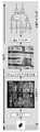
도 1은 역공학을 통한 칩의 넷-리스트 추출 과정에 대한 예시도이다.FIG. 1 is a diagram illustrating an example of a net-list extraction process of a chip through reverse engineering.
구체적으로 공격자는 칩을 디패키징하여 복수의 레이어로 분리한다. 그리고 공격자는 각 레이어에 대한 이미지 프로세싱(image processing)을 통하여, 해당 칩에 대응하는 넷-리스트를 추출한다. 이러한 과정을 통하여, 공격자는 해당 칩의 개발자가 디자인한 넷-리스트를 추출할 수 있다. 또는, 공격자는 칩에 모든 가능한 값을 입력하고, 출력되는 값을 통하여 내부 넷-리스트를 유추할 수 있다. 이러한 방법은 역공학 없이 입력되는 값 및 출력 값의 조합을 통하여 내부 넷-리스트를 추출할 수 있다.Specifically, an attacker decapsulates a chip into a plurality of layers. Then, the attacker extracts the net-list corresponding to the corresponding chip through image processing for each layer. Through this process, the attacker can extract the net-list designed by the developer of the chip. Alternatively, the attacker can input all possible values on the chip and infer the internal net-list through the output value. This method can extract the internal net-list through a combination of input values and output values without reverse engineering.
그러므로 칩 개발자는 공격자가 역공학 또는 입출력 값의 조합을 통하여 자신이 디자인한 넷-리스트를 추출하지 못하도록 보안(security) 방법을 사용할 수 있다.Therefore, a chip developer can use a security method to prevent an attacker from extracting a net-list that he designed through a combination of reverse engineering or input / output values.
이와 관련하여, 한국 등록특허공보 제10-1548211호(발명의 명칭: "역공학을 방지하기 위한 암호화 방법")는 역공학을 방지하기 위한 암호화 방법을 개시하고 있다.In this regard, Korean Patent Registration No. 10-1548211 (entitled "Encryption Method for Preventing Reverse Engineering") discloses an encryption method for preventing reverse engineering.
본 발명은 전술한 종래 기술의 문제점을 해결하기 위한 것으로서, 역공학을 방지하기 위하여 칩에 다양한 유형의 위장 게이트를 추가하는 위장 게이트에 기반한 칩, 칩에 대한 설계 방법 및 칩 설계 장치를 제공한다.Disclosure of Invention Technical Problem [8] Accordingly, the present invention has been made to solve the above-mentioned problems occurring in the prior art, and it is an object of the present invention to provide a chip based on a camouflage gate for adding various types of camouflage gates to a chip to prevent reverse engineering.
다만, 본 실시예가 이루고자 하는 기술적 과제는 상기된 바와 같은 기술적 과제로 한정되지 않으며, 또 다른 기술적 과제들이 존재할 수 있다.It should be understood, however, that the technical scope of the present invention is not limited to the above-described technical problems, and other technical problems may exist.
상술한 기술적 과제를 달성하기 위한 기술적 수단으로서, 본 발명의 제 1 측면에 따른 역공학을 방지하기 위한 위장 게이트에 기반한 칩은 복수의 위장 게이트가 포함되는 하나 이상의 클리크를 포함한다. 이때, 위장 게이트는 칩에 포함된 복수의 일반 게이트 중 어느 하나의 일반 게이트를 변환하여 생성된 것이고, 클리크에 포함된 타 위장 게이트와 연결된다.As a technical means to accomplish the above-mentioned technical problem, a camouflage gate-based chip for preventing reverse engineering according to the first aspect of the present invention includes at least one clique including a plurality of camouflage gates. At this time, the spoof gate is generated by converting one of the general gates included in the chip, and is connected to the other spoof gate included in the clek.
또한, 본 발명의 제 2 측면에 따른 위장 게이트에 기반한 칩의 역공학 방지 방법은 칩에 포함된 일반 게이트를 위장 게이트로 변환하는 단계; 일반 게이트에 대응하는 위장 게이트와 연결된 타 일반 게이트를 위장 게이트로 변환하는 단계; 및 일반 게이트에 대응하는 위장 게이트 및 타 일반 게이트에 대응하는 위장 게이트를 포함하는 클리크를 생성하는 단계를 포함한다. 이때, 칩은 하나 이상의 클리크를 포함한다.According to a second aspect of the present invention, there is provided a method for preventing reverse engineering of a chip based on a camouflage gate, comprising: converting a general gate included in the chip to a camouflage gate; Converting a general gate connected to the general gate to a general gate; And generating a clique comprising a camouflage gate corresponding to a common gate and a camouflage gate corresponding to another common gate. At this time, the chip includes one or more cliques.
그리고 본 발명의 제 3 측면에 따른 위장 게이트에 기반한 칩에 대한 설계 장치는 칩에 대한 설계 프로그램이 저장된 메모리 및 메모리에 저장된 프로그램을 실행하는 프로세서를 포함한다. 이때, 프로세서는 프로그램의 실행에 따라 칩에 포함된 일반 게이트를 위장 게이트로 변환하고, 일반 게이트에 대응하는 위장 게이트와 연결된 타 일반 게이트를 위장 게이트로 변환하며, 일반 게이트에 대응하는 위장 게이트 및 타 일반 게이트에 대응하는 위장 게이트를 포함하는 클리크를 생성한다. 그리고 칩은 하나 이상의 클리크를 포함한다.The apparatus for designing a chip based on a camouflage gate according to the third aspect of the present invention includes a processor for executing a program stored in a memory and a memory in which a design program for a chip is stored. At this time, according to the execution of the program, the processor converts the general gate included in the chip into the camouflage gate, converts the other common gate connected to the camouflage gate corresponding to the general gate to the camouflage gate, A clique is generated that includes a camouflage gate corresponding to a common gate. And the chip includes one or more cliques.
본 발명은 칩에 복수의 유형의 위장 게이트가 포함되도록 설계할 수 있다. 그러므로 본 발명은 공격자가 칩에 포함된 위장 게이트에 대한 실제 기능을 해석하기 어렵다. 또한, 본 발명은 칩 내의 해석 불가능 위장 게이트의 비율을 증가시켜 해당 칩의 보안 레벨을 향상시킬 수 있다.The present invention can be designed so that the chip includes a plurality of types of camouflage gates. Therefore, it is difficult for the attacker to interpret the actual function of the camouflaged gate included in the chip. Further, the present invention can improve the security level of the chip by increasing the ratio of the undetectable false gate in the chip.
도 1은 역공학을 통한 칩의 넷-리스트 추출 과정에 대한 예시도이다.
도 2는 종래의 위장 게이트 기반 보안 방법의 예시도이다.
도 3은 본 발명은 일 실시예에 따른 칩에 대한 칩 설계 장치의 블록도이다.
도 4는 본 발명의 일 실시예에 따른 위장 게이트를 포함하는 칩의 예시도이다.
도 5는 일반적인 위장 게이트 및 일반 게이트의 연결 관계의 예시도이다.
도 6은 본 발명의 일 실시예에 따른 위장 게이트 및 일반 게이트의 연결 관계의 예시도이다.
도 7은 본 발명의 일 실시예에 따른 다양한 위장 게이트의 연결관계를 포함하는 클리크의 예시도이다.
도 8은 본 발명의 일 실시예에 따른 위장 게이트에 기반한 칩의 역공학 방지 방법의 순서도이다.FIG. 1 is a diagram illustrating an example of a net-list extraction process of a chip through reverse engineering.
Figure 2 is an illustration of a conventional camouflage gate based security method.
3 is a block diagram of a chip design apparatus for a chip according to an embodiment of the present invention.
4 is an exemplary view of a chip including a camouflage gate according to an embodiment of the present invention.
5 is an exemplary view showing a connection relationship between a general camber gate and a general gate.
6 is an exemplary view illustrating a connection relationship between a camouflage gate and a general gate according to an embodiment of the present invention.
Figure 7 is an illustration of a clique that includes the connections of various camouflage gates in accordance with one embodiment of the present invention.
8 is a flowchart of a method for preventing reverse engineering of a chip based on a camouflage gate according to an embodiment of the present invention.
아래에서는 첨부한 도면을 참조하여 본 발명이 속하는 기술 분야에서 통상의 지식을 가진 자가 용이하게 실시할 수 있도록 본 발명의 실시예를 상세히 설명한다. 그러나 본 발명은 여러 가지 상이한 형태로 구현될 수 있으며 여기에서 설명하는 실시예에 한정되지 않는다. 그리고 도면에서 본 발명을 명확하게 설명하기 위해서 설명과 관계없는 부분은 생략하였으며, 명세서 전체를 통하여 유사한 부분에 대해서는 유사한 도면 부호를 붙였다.Hereinafter, embodiments of the present invention will be described in detail with reference to the accompanying drawings, which will be readily apparent to those skilled in the art. The present invention may, however, be embodied in many different forms and should not be construed as limited to the embodiments set forth herein. In order to clearly illustrate the present invention, parts not related to the description are omitted, and similar parts are denoted by like reference characters throughout the specification.
명세서 전체에서, 어떤 부분이 다른 부분과 "연결"되어 있다고 할 때, 이는 "직접적으로 연결"되어 있는 경우뿐 아니라, 그 중간에 다른 소자를 사이에 두고 "전기적으로 연결"되어 있는 경우도 포함한다. 또한 어떤 부분이 어떤 구성요소를 "포함"한다고 할 때, 이는 특별히 반대되는 기재가 없는 한 다른 구성요소를 제외하는 것이 아니라 다른 구성요소를 더 포함할 수 있는 것을 의미한다.Throughout the specification, when a part is referred to as being "connected" to another part, it includes not only "directly connected" but also "electrically connected" with another part in between . Also, when an element is referred to as "comprising ", it means that it can include other elements as well, without departing from the other elements unless specifically stated otherwise.
다음은 도 2를 참조하여 종래의 위장 게이트 기반 칩을 설명한다.The following describes a conventional camouflage gate-based chip with reference to FIG.
도 2는 종래의 위장 게이트 기반 보안 방법의 예시도이다.Figure 2 is an illustration of a conventional camouflage gate based security method.
역공학을 방지하기 위한 종래의 보안 방법 중에는 위장 게이트(camouflaged gate)를 이용하는 방법이 있다. 위장 게이트 기반 보안 방법은 공격자가 역공학을 통해 칩에서 넷-리스트를 추출하기 위하여 확인해야 하는 입출력 패턴을 증가시킨다. 그러므로 공격자는 위장 게이트 기반 보안 방법을 적용한 칩 내부의 넷 리스트를 추출하기 위하여, 모든 가능한 입력 패턴을 입력하고, 입력 패턴에 대응하는 출력 값을 통하여 칩 내부의 넷 리스트를 유추해야 한다.A conventional security method for preventing reverse engineering is to use a camouflaged gate. A spoofed gate-based security method increases the number of I / O patterns that an attacker must identify in order to extract the net-list from the chip through reverse engineering. Therefore, the attacker must input all possible input patterns and deduce the netlist inside the chip through the output value corresponding to the input pattern, in order to extract the netlist inside the chip applying the camouflage gate-based security method.
예를 들어, 위장 게이트 기반 보안 방법은 칩 내부의 기능을 수행하는 기능 경로(functional path)에 하나 이상의 클리크(clique)를 포함할 수 있다. 이때, 클리크는 해당 칩 내부에 포함되는 하나 이상의 게이트 중 일부를 위장 게이트(200, 210)로 변환하여 생성한 것일 수 있다. 이때, 위장 게이트(200, 210)는 특정 게이트의 기능을 포함하는 게이트로, 설계자가 디자인한 기능을 공격자가 알 수 없도록 설계된 것이다.For example, a spoofed gate-based security method may include one or more cliques in a functional path that performs a function inside the chip. At this time, the clique may be generated by converting a part of one or more gates included in the chip into the
도 2를 참조하면, 종래의 위장 게이트 기반 보안 방법은 각 위장 게이트(200, 210)이 하나 이상의 일반 게이트와 연결할 수 있다. 그러므로 공격자는 해당 위장 게이트(200, 210)가 어떠한 일을 하는지를 확인하기 위해서 역공학를 통하여 얻은 레이아웃 형상을 통하여 해당 위장 게이트(200, 210)가 실제로 어떤 기능을 수행하는지 알 수 없는 게이트이다.Referring to FIG. 2, a conventional camouflage gate based security method may connect each
그러므로 공격자는 해당 위장 게이트가 어떠한 일을 하는지를 확인하기 위해서 역공학을 통하여 추출된 정보에 기초하여 해당 위장 게이트의 기능을 추정하여야 한다. 구체적으로 공격자는 해당 칩의 주 입력에 적절한 입력 패턴을 입력하여 해당 위장 게이트의 입력을 정당화(justification)하고, 출력을 민감화(sensitization)하여 해당 위장 게이트를 분석하여야 한다.Therefore, the attacker must estimate the function of the camouflage gate based on the information extracted through reverse engineering to identify what the camouflage gate is doing. Specifically, the attacker must input the appropriate input pattern to the main input of the chip, justify the input of the corresponding gate, and sensitize the output to analyze the corresponding gate.
이때, 정당화는 특정 노드에 연결된 주 입력에 적절한 입력 패턴을 넣어 해당 노드의 값을 임의를 설정할 수 있는 것을 의미한다. 또한, 민감화는 특정 노드에 연결된 주 입력에 적절한 입력 패턴을 인가하여 나오는 주 출력들의 값에 기초하여, 해당 노드의 값이 무엇인지를 유추할 수 있는 것을 의미한다.In this case, the justification means that the value of the corresponding node can be arbitrarily set by inputting an appropriate input pattern to the main input connected to the specific node. In addition, the sensitization means that the value of the corresponding node can be inferred based on the value of the main outputs obtained by applying an appropriate input pattern to the main input connected to the specific node.
예를 들어, 위장 게이트(200, 210)는 공격자의 해석 가능성에 기초하여 독립 위장 게이트(isolate camouflaged gate), 부분 해석 가능(partially resolvable) 위장 게이트 및 해석 불가능(non-resolvable) 위장게이트로 구분할 수 있다.For example, the
이때, 독립 위장 게이트는 입력 정당화 및 출력 민감화가 모두 가능한 경우를 의미할 수 있다. 그러므로 독립 위장 게이트는 역공학을 통하여 추출된 정보를 통하여 공격자가 실제로 어떤 기능을 하는지 알 수 있다.At this time, the independent camouflage gate may mean that both input validation and output sensitization are possible. Therefore, an independent camouflage gate can learn what the attacker actually does through information extracted through reverse engineering.
또한, 부분 해석 가능 위장 게이트는 출력 민감화가 가능하며, 입력 정당화가 일부 가능한 경우를 의미한다. 즉, 부분 해석 가능 위장 게이트는 부분적으로만 해석이 가능한 위장 게이트이다. 예를 들어, 부분 해석 가능 위장 게이트는 해당 위장 게이트에 대응하는 역공학을 통하여 추출된 정보를 통하여, 해당 위장 게이트의 실제 기능이 XOR 게이트가 아님을 분석하지만, NOR 게이트 및 NAND 게이트 중 어떤 것인지를 알 수 없는 경우를 의미한다.In addition, the partially resolvable camouflage gate is capable of sensitizing the output and means that some of the input justification is possible. That is, the partially resolvable camouflage gate is a camouflage gate that can be partially analyzed. For example, the partially resolvable camouflage gate analyzes the information obtained through reverse engineering corresponding to the camouflage gate to analyze that the actual function of the camouflaged gate is not an XOR gate, but it does not know which of the NOR gate and the NAND gate Means unknown.
해석 불가능 위장 게이트는 해당 위장 게이트에 대한 입력 정당화 및 출력 민감화 중 하나가 불가능하거나, 모두 불가능 한 경우를 의미한다.A non-resolvable camouflage gate means that either one of the input justification and the output sensitization to the camouflaged gate is either impossible or impossible.
다시 도 2를 참조하면, 위장 게이트(200, 210)은 각각 일반 게이트와 연결된다. 그러므로 위장 게이트(200, 210)는 입력을 정당화하고, 출력을 민감화할 수 있는 입력 패턴을 통하여 용이하게 실제 기능을 해석할 수 있다.Referring again to FIG. 2, the
다음은 도 3 내지 도 7을 참조하여 본 발명의 일 실시예에 따른 역공학을 방지하기 위한 위장 게이트를 포함하는 칩(300)을 설명한다.3 to 7, a
도 3은 본 발명은 일 실시예에 따른 칩(300)에 대한 칩 설계 장치(310)의 블록도이다.3 is a block diagram of a
칩 설계 장치(310)는 설계자의 신호에 따라 칩(300) 내부의 회로 및 회로에 대한 넷-리스트를 설계한다. 이때, 칩(300)은 IC 칩 또는IP 칩이 될 수 있으나, 이에 한정된 것은 아니다. 또한, 칩 설계 장치(310)는 자동화된 설계 도구를 포함하거나, 기 설계된 칩(300)에 대한 추가적인 보안 기법을 적용하기 위한 설계 장치일 수 있으나, 이에 한정된 것은 아니다.The
구체적으로 칩(300)은 기능 경로 및 비기능 경로가 포함되도록 설계된다.Specifically, the
이때, 칩(300)의 주 입력(primary input)에 입력 패턴(input pattern)을 입력하면, 칩(300)은 칩(300)에 포함된 기 정의된 회로에 기초하여 주 출력(primary output) 을 통하여 출력 값을 출력할 수 있다. 이하에서 주 입력은 해당 칩(300)에서 입력 패턴을 최초로 입력 받은 노드 또는 게이트를 의미할 수 있다. 또한, 주 출력은 해당 칩(300)에서 입력 패턴에 대응하는 최종적인 출력 값을 출력하는 노드 또는 게이트를 의미할 수 있다.At this time, when an input pattern is input to the primary input of the
또한, 기능 경로 및 비기능 경로는 복수의 위장 게이트 및 일반 게이트의 집합인 클리크를 포함할 수 있다. 이때, 클리크에 포함되는 위장 게이트는 해석 불가능 위장 게이트 또는 부분 해석가능 위장 게이트일 수 있다.In addition, the functional path and the non-functional path may include a plurality of camouflage gates and a clique that is a collection of common gates. At this time, the camouflage gate included in the clic can be an unresolvable camouflage gate or a partially resolvable camouflage gate.
기능 경로는 칩(300)에 대응하여 정의된 로직에 기초한 경로가 될 수 있다. 즉, 기능 경로는 로직에 기초하여 입력 패턴이 해당 칩(300)을 통과하여 입력 패턴에 대응하는 출력 값을 산출할 수 있는 하나 이상의 게이트를 포함할 수 있다.The functional path may be a path based on logic defined in correspondence with the
또한, 비기능 경로는 기능 경로에 대응되는 개념으로 칩(300)에 포함되었으나, 실제 칩에 대응하는 기능을 수행하지 않는 경로일 수 있다. 즉, 비기능 경로의 각 게이트는 그 출력 값이 최종적으로 칩(300)의 기능에 영향을 미치지 않을 수 있다.Also, the non-functional path may be a path included in the
이때, 비기능 경로는 'false path'가 될 수 있다. 또는, 비기능 경로는 기정의된 로직과 상관없이 칩(300)의 설계 시 자동화된 설계 도구를 통하여 자동으로 추가된 경로일 수 있으나, 이에 한정된 것은 아니다.At this time, the non-functional path may be a 'false path'. Alternatively, the non-functional path may be, but is not limited to, an automatically added path through an automated design tool when designing the
도 4는 본 발명의 일 실시예에 따른 위장 게이트를 포함하는 칩(300)의 예시도이다.4 is an illustration of a
칩(300)은 칩(300)에 포함된 복수의 일반 게이트(410) 중 일부를 위장 게이트(400)로 변환하여 클리크를 생성할 수 있다. 즉, 칩(300)은 해당 칩(300)의 입력 패턴에 대응하는 입력 데이터가 복수의 위장 게이트(400)를 포함하는 클리크를 통과하도록 설계된 것일 수 있다.
예를 들어, 일반 게이트(410)는 NOT 게이트, AND 게이트, OR 게이트, XOR 게이트, NOR 게이트, NAND 게이트 및 INV 게이트 등의 유형에 대응되는 것이 될 수 있으나, 이에 한정된 것은 아니다.For example, the
또한, 위장 게이트(400)는 일반 게이트(410)에 대응하는 것일 수 있다. 예를 들어, 칩(300)이 XOR 게이트, NAND 게이트 및 NOR 게이트가 포함되도록 설계된다면, 위장 게이트(400)는 XOR 게이트, NAND 게이트 및 NOR 게이트 중 어느 하나의 기능을 수행하며, 공격자가 실제 기능을 알 수 없도록 설계된 것일 수 있다.In addition, the
구체적으로, 위장 게이트(400)는 역공학을 통하여 공격자가 어떠한 기능을 하는지 판단할 수 없도록 정의된 게이트일 수 있다. 예를 들어, 위장 게이트(400)는 이미지 기반 역공학을 통하여 얻은 레이아웃(layout)의 형상을 통하여 해당 게이트가 어떤 유형의 게이트인지 알 수 없는 것을 의미한다.Specifically, the
예를 들어, 위장 게이트(400)는 칩(300)의 설계자의 디자인에 따라, XOR 게이트, NAND 게이트 및 NOR 게이트 중 하나의 기능을 수행하도록 설계된 게이트일 수 있다. 즉, 해당 위장 게이트(400)의 실제 기능은 XOR 게이트, NOR 게이트 및 NAND 게이트 중 어느 하나로 정의되나, 역공학을 통하여 추출된 정보로 공격자가 해당 위장 게이트(400)의 실제 기능이 XOR, NOR 및 NAND 중 어떤 기능에 대응하는 것인지 알 수 없을 수 있다.For example, the
그러므로 공격자는 해당 위장 게이트가 어떠한 일을 하는지를 확인하기 위해서 역공학을 통하여 추출된 정보에 기초하여 해당 위장 게이트의 기능을 추정하여야 한다. 구체적으로 공격자는 해당 칩의 주 입력에 적절한 입력 패턴을 입력하여 해당 위장 게이트의 입력을 정당화(justification)하고, 출력을 민감화(sensitization)하여 해당 위장 게이트를 분석하여야 한다.Therefore, the attacker must estimate the function of the camouflage gate based on the information extracted through reverse engineering to identify what the camouflage gate is doing. Specifically, the attacker must input the appropriate input pattern to the main input of the chip, justify the input of the corresponding gate, and sensitize the output to analyze the corresponding gate.
이때, 정당화는 특정 노드 또는 특정 노드에 연결된 주 입력에 적절한 입력 패턴을 넣어 해당 노드의 값을 임의를 설정할 수 있는 것을 의미한다. 또한, 민감화는 적절한 입력 패턴에 대응하는 특정 노드의 출력 값을 통하여 해당 노드의 값이 무엇인지를 유추할 수 있다는 것을 의미한다.In this case, the justification means that the value of the corresponding node can be arbitrarily set by inputting an appropriate input pattern to the main input connected to the specific node or the specific node. In addition, the sensitization means that the value of the corresponding node can be inferred through the output value of the specific node corresponding to the appropriate input pattern.
한편, 앞에서 살펴본 바와 같이 위장 게이트는 유형에 따라 하나의 일반 게이트에 대응되도록 정의된다. 그리고 위장 게이트는 해당 위장 게이트가 포함되는 임의의 경로는 해당 경로에 포함되는 타 위장 게이트와 연결된다.On the other hand, as described above, the camouflage gate is defined to correspond to one common gate depending on the type. And the arbitrary path including the corresponding camouflage gate is connected to the other camouflage gate included in the corresponding path.
이때, 위장 게이트 및 일반 게이트의 연결 관계는 도 5 및 도 6을 참조하여 상세하게 설명한다.At this time, the connection relation between the camouflage gate and the general gate will be described in detail with reference to FIG. 5 and FIG.
도 5는 일반적인 위장 게이트 간의 연결 관계의 예시도이다.Figure 5 is an exemplary view of the connection relationship between common camouflage gates.
예를 들어, 임의의 클리크는 제 1 위장 게이트, 제 2 위장 게이트 및 제 3 위장 게이트가 포함되도록 생성될 수 있다. 이때, 제 1 위장 게이트, 제 2 위장 게이트 및 제 3 위장 게이트의 유형은 제 1 유형으로 동일할 수 있다. 이때, 제 1 유형은 XOR 게이트, NAND 게이트 및 NOR 게이트 중 어느 하나에 대응되도록 정의된 것일 수 있다. 즉, 제 1 위장 게이트, 제 2 위장 게이트 및 제 3 위장 게이트는 XOR 게이트, NAND 게이트 및 NOR 게이트 중 어느 하나에 대응하는 것이다.For example, any clique may be generated to include a first spoof gate, a second spoof gate, and a third spoof gate. At this time, the first camouflage gate, the second camouflage gate, and the third camouflage gate may be of the same type. At this time, the first type may be defined to correspond to any one of XOR gate, NAND gate, and NOR gate. That is, the first, second and third camouflage gates correspond to either the XOR gate, the NAND gate, or the NOR gate.
제 1 유형은 진리표는 [표 1]과 같다.The truth table for the first type is shown in [Table 1].
제 3 위장 게이트의 입력이 '00'이 되도록 할 수 있다. 그리고 공격자는 제 3 위장 게이트의 출력에 따라, 제 3 위장 게이트의 기능이 XOR인지 여부를 판단할 수 있다. 이와 같이, 연결관계에 있는 모든 위장 게이트의 유형이 동일한 경우, 제 3 위장 게이트는 부분 해석 가능 위장 게이트가 될 수 있다. The input of the third camouflage gate may be '00'. Then, the attacker can determine whether the function of the third camouflage gate is XOR according to the output of the third camouflage gate. Thus, if all the types of camouflage gates in the connection are of the same type, then the third camouflage gate can be a partially resolvable camouflage gate.
도 6은 본 발명의 일 실시예에 따른 위장 게이트 간의 연결 관계의 예시도이다.6 is an exemplary view illustrating a connection relationship between camouflage gates according to an embodiment of the present invention.
반면에, 클리크는 제 1 위장 게이트, 제 2 위장 게이트 및 제 3 위장 게이트가 포함되도록 생성될 수 있다. 이때, 제 1 위장 게이트 및 제 2 위장 게이트는 유형이 제 1 유형이며, 제 3 위장 게이트의 유형은 제 2 유형으로 서로 상이할 수 있다. 즉, 제 1 위장 게이트 및 제 2 위장 게이트는 각각 상이한 유형의 제 3 위장 게이트와 연결될 수 있다.On the other hand, the clique may be generated to include a first camouflage gate, a second camouflage gate, and a third camouflage gate. At this time, the first camouflage gate and the second camouflage gate may be of the first type and the third camouflage gate type may be different of the second type. That is, the first and second camouflage gates may each be connected to a different type of third camouflage gate.
제 1 유형은 앞에서 설명한 바와 같이, XOR 게이트, NAND 게이트 및 NOR 게이트를 포함하는 것이며, 제 2 유형은 XOR 게이트, AND 게이트 및 OR 게이트를 포함하는 것이다. 즉, 제 1 위장 게이트 및 제 2 위장 게이트는 XOR 게이트, NAND 게이트 및 NOR 게이트 중 어느 하나와 대응되는 것일 수 있다. 또한, 제 3 위장 게이트는 XOR 게이트, AND 게이트 및 OR 게이트 중 어느 하나와 대응되는 것일 수 있다.The first type includes XOR gates, NAND gates and NOR gates as described above, and the second type includes XOR gates, AND gates, and OR gates. That is, the first and second camouflage gates may correspond to any one of the XOR gate, the NAND gate, and the NOR gate. Further, the third camouflage gate may correspond to any one of the XOR gate, the AND gate, and the OR gate.
이때, 제 1 유형은 진리표는 앞에서 설명한 [표 1]과 같으며, 제 2 유형의 진리표는 [표 2]와 같다.In this case, the truth table of the first type is as shown in [Table 1], and the truth table of the second type is as shown in [Table 2].
도 6을 참조하면, 제 1 위장 게이트 및 제 2 위장 게이트는 유형이 상이한 제 3 위장 게이트와 연결될 수 있다.Referring to FIG. 6, the first camouflage gate and the second camouflage gate may be connected to a third camouflage gate of a different type.
도 5를 참조하여 설명한 것과 유사하게, 공격자는 제 1 위장 게이트 및 제 2 위장 게이트에 모두 '11'이 인가하여 제 3 위장 게이트의 입력이 '00'이 되도록 할 수 있다. 이때, 제 2 유형의 제 3 위장 게이트에 '00'이 입력되면, 출력 값은 '0'이 된다. 그러므로 공격자는 제 3 위장 게이트의 출력에 따라, 제 3 위장 게이트의 기능을 판단할 수 없게 된다. 이와 같이, 연결관계에 있는 위장 게이트의 유형이 상이한 경우, 제 3 위장 게이트는 해석 불가능 위장 게이트가 될 수 있다.Similar to the case described with reference to FIG. 5, the attacker may apply '11' to both the first and second camouflage gates so that the input of the third camouflage gate is '00'. At this time, if '00' is input to the third type of the third camouflage gate, the output value becomes '0'. Therefore, the attacker can not judge the function of the third camouflage gate according to the output of the third camouflage gate. Thus, if the type of camouflage gates in the connection are different, then the third camouflage gate may be a non-resolvable camouflage gate.
이와 같이, 서로 상이한 유형의 위장 게이트가 연결되면, 해당 클리크에 포함된 위장 게이트는 해석 불가능 위장 게이트가 될 수 있다. 그러므로 칩(300)의 보안성을 향상시키기 위하여, 칩(300)에 포함된 위장 게이트는 유형이 상이한 다른 위장 게이트와 연결관계를 가질 수 있다.Thus, when different types of camouflage gates are connected, the camouflage gates included in the clik can be non-resolvable camouflage gates. Therefore, in order to improve the security of the
구체적으로 칩(300)에 포함된 복수의 일반 게이트 중 일부를 위장 게이트로 변환하여 클리크를 생성할 수 있다. 이때, 해당 클리크에 포함된 임의의 위장 게이트는 다른 위장 게이트와 연결될 수 있다.Specifically, a part of a plurality of general gates included in the
또한, 해당 클리크에 포함된 위장 게이트는 각각 기정의된 유형에 대응하는 것일 수 있다. 해당 클리크에 포함된 위장 게이트의 유형은 연결관계에 있는 타 위장 게이트의 유형과 상이할 수 있다.In addition, the camouflage gates included in the cleck may each correspond to a predetermined type. The type of camouflage gate included in the cleck may be different from the type of camouflage gate in the connection.
예를 들어, 해당 클리크는 제 1 위장 게이트 및 제 1 위장 게이트의 단부와 연결되며, 유형이 상이한 제 2 위장 게이트를 포함할 수 있다. 즉, 제 2 위장 게이트는 제 1 위장 게이트를 통과한 입력 데이터에 대한 출력 값을 다시 입력 데이터로 이용할 수 있다. 또한, 제 1 유형은 XOR 게이트, NAND 게이트 및 NOR 게이트 중 어느 하나에 대응되도록 정의되며, 제 2 유형은 XOR 게이트, AND 게이트 및 OR 게이트 중 어느 하나에 대응되도록 정의된 것일 수 있다.For example, the clique may comprise a first camouflage gate and a second camouflage gate connected to an end of the first camouflage gate and of a different type. That is, the second spoof gate can use the output value of the input data passed through the first spoof gate as input data again. Also, the first type may be defined to correspond to one of the XOR gate, the NAND gate, and the NOR gate, and the second type may be defined to correspond to one of the XOR gate, the AND gate, and the OR gate.
추가 실시 예로, 해당 클리크는 제 1 위장 게이트, 제 2 위장 게이트 및 제 3 위장 게이트를 포함할 수 있다. 제 3 위장 게이트는 제 1 위장 게이트의 단부 및 제 2 위장 게이트의 단부와 연결될 수 있다. 그러므로 제 3 위장 게이트는 제 1 위장 게이트를 통과하여 산출된 제 1 출력 값 및 제 2 위장 게이트를 통과하여 산출된 제 2 출력 값을 입력 데이터로 하는 게이트일 수 있다.In a further embodiment, the cliee may include a first camouflage gate, a second camouflage gate, and a third camouflage gate. The third camouflage gate may be connected to the end of the first camouflage gate and the end of the second camouflage gate. Therefore, the third spoof gate may be a gate having the first output value calculated through the first spoof gate and the second output value calculated through the second spoof gate as the input data.
이때, 제 3 위장 게이트는 제 1 위장 게이트와 상이한 유형일 수 있다. 또한, 제 3 위장 게이트는 제 2 위장 게이트와 상이한 유형일 수 있다. 제 1 위장 게이트 및 제 2 위장 게이트의 유형은 동일할 수도 있으며, 상이할 수도 있다.At this time, the third camouflage gate may be of a different type than the first camouflage gate. Also, the third camouflage gate may be of a different type than the second camouflage gate. The types of first and second camouflage gates may be the same or different.
이와 같이, 클리크는 서로 상이한 유형의 위장 게이트와 연결되는 하나 이상의 위장 게이트를 포함할 수 있다. 그러므로 해당 클리크에 포함된 위장 게이트는 해석 불가능 위장 게이트가 될 수 있다.As such, the cliks may include one or more camouflage gates connected to camouflage gates of different types. Therefore, the camouflage gate included in the corresponding clique may be an unresolvable camouflage gate.
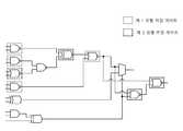
도 7은 본 발명의 일 실시예에 따른 다양한 위장 게이트의 연결관계를 포함하는 클리크의 예시도이다.Figure 7 is an illustration of a clique that includes the connections of various camouflage gates in accordance with one embodiment of the present invention.
앞에서 설명한 복수의 위장 게이트의 연결 관계는 복합적으로 사용이 가능하다. 도 7을 참조하면 클리크는 제 1 유형의 위장 게이트(700, 710, 740, 750), 제 2 유형의 위장 게이트(720, 730, 760, 770) 및 일반 게이트를 포함할 수 있다. 또한, 제 1 유형 및 제 2 유형은 각각 상이할 수 있다.The connection relationships of the plurality of camouflage gates described above can be used in combination. Referring to FIG. 7, Clk may include a first type of camouflage gate 700, 710, 740, 750, a second type camouflage gate 720, 730, 760, 770 and a common gate. Further, the first type and the second type may be different from each other.
다음은 도 8을 참조하여 본 발명의 일 실시예에 따른 위장 게이트에 기반한 칩(300)의 역공학 방지 방법을 설명한다.Next, referring to FIG. 8, a method for preventing reverse engineering of the
도 8은 본 발명의 일 실시예에 따른 위장 게이트에 기반한 칩(300)의 역공학 방지 방법의 순서도이다.8 is a flowchart of a method for preventing reverse engineering of a
칩(300)은 칩(300)에 포함된 일반 게이트를 위장 게이트로 변환한다(S800).The
또한, 칩(300)은 일반 게이트에 대응하는 위장 게이트와 연결된 타 일반 게이트를 위장 게이트로 변환한다(S810).In addition, the
그리고 칩(300)은 일반 게이트에 대응하는 위장 게이트 및 타 일반 게이트에 대응하는 위장 게이트를 포함하는 클리크를 생성한다(S820). 이때, 일반 게이트에 대응하는 위장 게이트의 유형 및 타 일반 게이트에 대응하는 위장 게이트의 유형은 서로 상이할 수 있다.Then, the
그리고 유형은 NOT 게이트, AND 게이트, OR 게이트, XOR 게이트, NOR 게이트, NAND 게이트 및 INV 게이트 중 하나 이상에 대응되는 것일 수 있다.And the type may correspond to one or more of a NOT gate, an AND gate, an OR gate, an XOR gate, a NOR gate, a NAND gate, and an INV gate.
이때, 칩(300)은 하나 이상의 클리크를 포함할 수 있다.At this point, the
다음은 도 3을 참조하여, 본 발명의 일 실시예에 따른 칩 설계 장치(310)를 설명한다.3, a
다시 도 3을 참조하면, 칩 설계 장치(310)는 메모리(330) 및 프로세서(320)를 포함한다.Referring again to FIG. 3, the
이때, 메모리(330)는 칩(300)에 대한 설계 프로그램을 저장한다. 이때, 메모리(330)는 전원이 공급되지 않아도 저장된 정보를 계속 유지하는 비휘발성 저장장치 및 저장된 정보를 유지하기 위하여 전력이 필요한 휘발성 저장장치를 통칭하는 것이다At this time, the
또한, 칩 설계 장치(310)는 입력 모듈(미도시)을 더 포함할 수 있다. 이때, 입력 모듈(미도시)은 칩(300)의 설계자의 신호를 수신하기 위하여 활용될 수 있다. 이때, 입력 모듈(미도시)은 키보드, 마우스와 같은 입력 장치와 연결될 수 있다.In addition, the
칩(300)은 칩 설계 장치(310)를 통하여 회로가 설계되는 칩(300)이 될 수 있다. 또는, 칩(300)은 기 설계된 칩(300)으로 칩 설계 장치(310)에 의하여 칩(300)에 포함된 일부 일반 게이트를 위장 게이트로 변환하는 것일 수 있다.The
한편, 프로세서(320)는 칩(300)에 포함된 일반 게이트를 위장 게이트로 변환한다. 이때, 칩(300)에 포함된 일반 게이트는 기정의된 로직에 대응되는 것일 수 있다.Meanwhile, the
그리고 프로세서(320)는 일반 게이트에 대응하는 위장 게이트와 연결된 타 일반 게이트를 위장 게이트로 변환한다.The
프로세서(320)는 일반 게이트에 대응하는 위장 게이트 및 타 일반 게이트에 대응하는 위장 게이트를 포함하는 클리크를 생성한다. 이때, 칩(300)은 하나 이상의 클리크를 포함하도록 정의된다.
본 발명의 일 실시예에 따른 역공학을 방지하기 위한 위장 게이트에 기반한 칩(300), 칩(300)에 대한 설계 방법 및 칩 설계 장치(310)는 칩(300)에 복수의 유형의 위장 게이트가 포함되도록 설계할 수 있다. 그러므로 역공학을 방지하기 위한 위장 게이트에 기반한 칩(300), 칩(300)에 대한 설계 방법 및 칩 설계 장치(310)는 공격자가 칩(300)에 포함된 위장 게이트에 대한 실제 기능을 해석하기 어렵다. 또한, 역공학을 방지하기 위한 위장 게이트에 기반한 칩(300), 칩(300)에 대한 설계 방법 및 칩 설계 장치(310)는 칩(300) 내의 해석 불가능 위장 게이트의 비율을 증가시켜 해당 칩(300)의 보안 레벨을 향상시킬 수 있다.A
본 발명의 일 실시예는 컴퓨터에 의해 실행되는 프로그램 모듈과 같은 컴퓨터에 의해 실행가능한 명령어를 포함하는 기록 매체의 형태로도 구현될 수 있다. 컴퓨터 판독 가능 매체는 컴퓨터에 의해 액세스될 수 있는 임의의 가용 매체일 수 있고, 휘발성 및 비휘발성 매체, 분리형 및 비분리형 매체를 모두 포함한다. 또한, 컴퓨터 판독가능 매체는 컴퓨터 저장 매체를 포함할 수 있다. 컴퓨터 저장 매체는 컴퓨터 판독가능 명령어, 데이터 구조, 프로그램 모듈 또는 기타 데이터와 같은 정보의 저장을 위한 임의의 방법 또는 기술로 구현된 휘발성 및 비휘발성, 분리형 및 비분리형 매체를 모두 포함한다.One embodiment of the present invention may also be embodied in the form of a recording medium including instructions executable by a computer, such as program modules, being executed by a computer. Computer readable media can be any available media that can be accessed by a computer and includes both volatile and nonvolatile media, removable and non-removable media. The computer-readable medium may also include computer storage media. Computer storage media includes both volatile and nonvolatile, removable and non-removable media implemented in any method or technology for storage of information such as computer readable instructions, data structures, program modules or other data.
본 발명의 방법 및 시스템은 특정 실시예와 관련하여 설명되었지만, 그것들의 구성 요소 또는 동작의 일부 또는 전부는 범용 하드웨어 아키텍쳐를 갖는 컴퓨터 시스템을 사용하여 구현될 수 있다.While the methods and systems of the present invention have been described in connection with specific embodiments, some or all of those elements or operations may be implemented using a computer system having a general purpose hardware architecture.
전술한 본 발명의 설명은 예시를 위한 것이며, 본 발명이 속하는 기술분야의 통상의 지식을 가진 자는 본 발명의 기술적 사상이나 필수적인 특징을 변경하지 않고서 다른 구체적인 형태로 쉽게 변형이 가능하다는 것을 이해할 수 있을 것이다. 그러므로 이상에서 기술한 실시예들은 모든 면에서 예시적인 것이며 한정적이 아닌 것으로 이해해야만 한다. 예를 들어, 단일형으로 설명되어 있는 각 구성 요소는 분산되어 실시될 수도 있으며, 마찬가지로 분산된 것으로 설명되어 있는 구성 요소들도 결합된 형태로 실시될 수 있다.It will be understood by those skilled in the art that the foregoing description of the present invention is for illustrative purposes only and that those of ordinary skill in the art can readily understand that various changes and modifications may be made without departing from the spirit or essential characteristics of the present invention. will be. It is therefore to be understood that the above-described embodiments are illustrative in all aspects and not restrictive. For example, each component described as a single entity may be distributed and implemented, and components described as being distributed may also be implemented in a combined form.
본 발명의 범위는 상기 상세한 설명보다는 후술하는 특허청구범위에 의하여 나타내어지며, 특허청구범위의 의미 및 범위 그리고 그 균등 개념으로부터 도출되는 모든 변경 또는 변형된 형태가 본 발명의 범위에 포함되는 것으로 해석되어야 한다.The scope of the present invention is defined by the appended claims rather than the detailed description and all changes or modifications derived from the meaning and scope of the claims and their equivalents are to be construed as being included within the scope of the present invention do.
300: 칩
310: 칩 설계 장치
320: 프로세서
330: 메모리300: chip
310: chip design device
320: Processor
330: Memory
Claims (12)
Translated fromKorean복수의 위장 게이트가 포함되는 하나 이상의 클리크(clique)를 포함하되,
상기 위장 게이트는 상기 칩에 포함된 복수의 일반 게이트 중 어느 하나의 일반 게이트를 변환하여 생성된 것이고, 상기 클리크(clique)에 포함된 타 위장 게이트와 연결되는 것이며,
적어도 하나의 상기 클리크는 제 1 위장 게이트 및 제 2 위장 게이트를 포함하고,
상기 제 2 위장 게이트는 상기 제 1 위장 게이트를 통과한 입력 데이터에 대응하는 출력 값을 수신하도록 상기 제 1 위장 게이트와 연결되는 것이고,
상기 제 1 위장 게이트의 유형 및 상기 제 2 위장 게이트의 유형은 서로 상이한 것인, 위장 게이트 기반 칩.
A chip based on a camouflage gate for preventing reverse engineering,
At least one clique comprising a plurality of camouflage gates,
Wherein the camouflage gate is formed by converting a common gate of any one of a plurality of common gates included in the chip and is connected to another camouflage gate included in the clique,
Wherein at least one of the cliks comprises a first camouflage gate and a second camouflage gate,
The second camouflage gate is coupled to the first camouflage gate to receive an output value corresponding to input data passed through the first camouflage gate,
Wherein the type of the first camouflage gate and the type of the second camouflage gate are different from each other.
상기 위장 게이트의 유형은 상기 연결되는 타 위장 게이트의 유형과 상이한, 위장 게이트 기반 칩.
The method according to claim 1,
Wherein the type of the camouflage gate is different from the type of the other camouflage gate to which it is connected.
상기 유형은 NOT 게이트, AND 게이트, OR 게이트, XOR 게이트, NOR 게이트, NAND 게이트 및 INV 게이트 중 하나 이상에 대응되는, 위장 게이트 기반 칩.
3. The method of claim 2,
Wherein the type corresponds to one or more of a NOT gate, an AND gate, an OR gate, an XOR gate, a NOR gate, a NAND gate, and an INV gate.
상기 칩에 둘 이상의 클리크가 포함되며,
상기 둘 이상의 클리크 중 적어도 하나는 제 3 위장 게이트, 제 4 위장 게이트, 및 상기 제 3 위장 게이트의 출력 단과 상기 제 4 위장 게이트의 출력 단과 각각 연결되는 제 5 위장 게이트를 포함하고,
상기 제 5 위장 게이트는 상기 제 3 위장 게이트 및 상기 제 4 위장 게이트로부터 각각 산출된 출력 값을 입력 데이터로 통과시키고, 상기 입력 데이터에 대응하는 출력 값을 산출하며,
상기 제 5 위장 게이트의 유형은 상기 제 3 위장 게이트의 유형 및 상기 제 4 위장 게이트의 유형 중 적어도 하나와 상이한, 위장 게이트 기반 칩.
The method according to claim 1,
Wherein the chip includes at least two cliks,
Wherein at least one of the two or more cliks comprises a third camouflage gate, a fourth camouflage gate, and a fifth camouflage gate connected respectively to an output end of the third camouflage gate and an output end of the fourth camouflage gate,
The fifth camouflage gate passes output values respectively calculated from the third camouflage gate and the fourth camouflage gate as input data, calculates an output value corresponding to the input data,
Wherein the type of the fifth camouflage gate is different from at least one of the type of the third camouflage gate and the type of the fourth camouflage gate.
상기 클리크에 포함된 위장 게이트는 해석 불가능 위장 게이트(non-resolvable) 또는 부분 해석가능(partially resolvable) 위장 게이트인, 위장 게이트 기반 칩.
The method according to claim 1,
Wherein the camouflage gate included in the clic is a non-resolvable or partially resolvable camouflage gate.
칩에 포함된 일반 게이트를 위장 게이트로 변환하는 단계;
상기 일반 게이트에 대응하는 위장 게이트와 연결된 타 일반 게이트를 위장 게이트로 변환하는 단계; 및
상기 일반 게이트에 대응하는 위장 게이트 및 상기 타 일반 게이트에 대응하는 위장 게이트를 포함하는 클리크(clique)를 생성하는 단계를 포함하되,
상기 칩은 하나 이상의 클리크(clique)를 포함하며,
적어도 하나의 상기 클리크는 제 1 위장 게이트 및 제 2 위장 게이트를 포함하고,
상기 제 2 위장 게이트는 상기 제 1 위장 게이트를 통과한 입력 데이터에 대응하는 출력 값을 수신하도록 상기 제 1 위장 게이트와 연결되는 것이고,
상기 제 1 위장 게이트의 유형 및 상기 제 2 위장 게이트의 유형은 서로 상이한 것인, 칩의 역공학 방지 방법.
A method for preventing reverse engineering of a chip based on a camouflage gate based on a camouflage gate,
Converting a common gate included in the chip into a camouflage gate;
Converting a general gate connected to the general gate to a general gate; And
Generating a clique comprising a camouflage gate corresponding to the common gate and a camouflage gate corresponding to the other common gate,
Wherein the chip comprises at least one clique,
Wherein at least one of the cliks comprises a first camouflage gate and a second camouflage gate,
The second camouflage gate is coupled to the first camouflage gate to receive an output value corresponding to input data passed through the first camouflage gate,
Wherein the type of the first camouflage gate and the type of the second camouflage gate are different from each other.
상기 일반 게이트에 대응하는 위장 게이트의 유형 및 상기 타 일반 게이트에 대응하는 위장 게이트의 유형은 서로 상이한, 칩의 역공학 방지 방법.
8. The method of claim 7,
Wherein the type of camouflage gate corresponding to the common gate and the type of camouflage gate corresponding to the other common gate are different from each other.
상기 유형은 NOT 게이트, AND 게이트, OR 게이트, XOR 게이트, NOR 게이트, NAND 게이트 및 INV 게이트 중 하나 이상에 대응되는, 칩의 역공학 방지 방법.
9. The method of claim 8,
Wherein the type corresponds to one or more of a NOT gate, an AND gate, an OR gate, an XOR gate, a NOR gate, a NAND gate, and an INV gate.
상기 클리크에 포함된 위장 게이트는 해석 불가능 위장 게이트(non-resolvable) 또는 부분 해석가능(partially resolvable) 위장 게이트인, 칩의 역공학 방지 방법.
8. The method of claim 7,
Wherein the camouflage gate included in the clique is a non-resolvable or partially resolvable camouflage gate.
칩에 대한 설계 프로그램이 저장된 메모리 및
상기 메모리에 저장된 프로그램을 실행하는 프로세서를 포함하되,
상기 프로세서는 상기 프로그램의 실행에 따라 칩에 포함된 일반 게이트를 위장 게이트로 변환하고, 상기 일반 게이트에 대응하는 위장 게이트와 연결된 타 일반 게이트를 위장 게이트로 변환하며, 상기 일반 게이트에 대응하는 위장 게이트 및 상기 타 일반 게이트에 대응하는 위장 게이트를 포함하는 클리크(clique)를 생성하되,
상기 칩은 하나 이상의 클리크(clique)를 포함하며,
적어도 하나의 상기 클리크는 제 1 위장 게이트 및 제 2 위장 게이트를 포함하고,
상기 제 2 위장 게이트는 상기 제 1 위장 게이트를 통과한 입력 데이터에 대응하는 출력 값을 수신하도록 상기 제 1 위장 게이트와 연결되는 것이고,
상기 제 1 위장 게이트의 유형 및 상기 제 2 위장 게이트의 유형은 서로 상이한 것인, 칩 설계 장치.
In a design apparatus for a chip based on a camouflage gate,
The design program for the chip is stored in memory and
And a processor for executing a program stored in the memory,
The processor converts the general gate included in the chip into a camouflage gate, converts another general gate connected to the camouflage gate corresponding to the general gate to a camouflage gate, And a camouflage gate corresponding to the other general gate,
Wherein the chip comprises at least one clique,
Wherein at least one of the cliks comprises a first camouflage gate and a second camouflage gate,
The second camouflage gate is coupled to the first camouflage gate to receive an output value corresponding to input data passed through the first camouflage gate,
Wherein the type of the first camouflage gate and the type of the second camouflage gate are different from each other.
Priority Applications (1)
| Application Number | Priority Date | Filing Date | Title |
|---|---|---|---|
| KR1020170028682AKR101868548B1 (en) | 2017-03-07 | 2017-03-07 | Chip, method and apparatus of chip design technique based on camouflaged gate for prventing reverse engineering |
Applications Claiming Priority (1)
| Application Number | Priority Date | Filing Date | Title |
|---|---|---|---|
| KR1020170028682AKR101868548B1 (en) | 2017-03-07 | 2017-03-07 | Chip, method and apparatus of chip design technique based on camouflaged gate for prventing reverse engineering |
Publications (1)
| Publication Number | Publication Date |
|---|---|
| KR101868548B1true KR101868548B1 (en) | 2018-06-19 |
Family
ID=62790246
Family Applications (1)
| Application Number | Title | Priority Date | Filing Date |
|---|---|---|---|
| KR1020170028682AExpired - Fee RelatedKR101868548B1 (en) | 2017-03-07 | 2017-03-07 | Chip, method and apparatus of chip design technique based on camouflaged gate for prventing reverse engineering |
Country Status (1)
| Country | Link |
|---|---|
| KR (1) | KR101868548B1 (en) |
Cited By (1)
| Publication number | Priority date | Publication date | Assignee | Title |
|---|---|---|---|---|
| US11977614B2 (en) | 2021-09-20 | 2024-05-07 | International Business Machines Corporation | Circuit design watermarking |
Citations (3)
| Publication number | Priority date | Publication date | Assignee | Title |
|---|---|---|---|---|
| US20030214002A1 (en)* | 2002-05-14 | 2003-11-20 | Hrl Laboratories, Llc | Integrated circuit with reverse engineering protection |
| US20160197616A1 (en)* | 2009-02-24 | 2016-07-07 | Syphermedia International, Inc. | Physically unclonable camouflage structure and methods for fabricating same |
| US20160224407A1 (en)* | 2013-09-11 | 2016-08-04 | New York University | System, method and computer-accessible medium for fault analysis driven selection of logic gates to be camouflaged |
- 2017
- 2017-03-07KRKR1020170028682Apatent/KR101868548B1/ennot_activeExpired - Fee Related
Patent Citations (3)
| Publication number | Priority date | Publication date | Assignee | Title |
|---|---|---|---|---|
| US20030214002A1 (en)* | 2002-05-14 | 2003-11-20 | Hrl Laboratories, Llc | Integrated circuit with reverse engineering protection |
| US20160197616A1 (en)* | 2009-02-24 | 2016-07-07 | Syphermedia International, Inc. | Physically unclonable camouflage structure and methods for fabricating same |
| US20160224407A1 (en)* | 2013-09-11 | 2016-08-04 | New York University | System, method and computer-accessible medium for fault analysis driven selection of logic gates to be camouflaged |
Non-Patent Citations (1)
| Title |
|---|
| J. Rajendran et al. ‘VLSI Testing based Security Metric for IC Camouflaging’, Test Conference, 2013 IEEE International, 2013.11.04.* |
Cited By (1)
| Publication number | Priority date | Publication date | Assignee | Title |
|---|---|---|---|---|
| US11977614B2 (en) | 2021-09-20 | 2024-05-07 | International Business Machines Corporation | Circuit design watermarking |
Similar Documents
| Publication | Publication Date | Title |
|---|---|---|
| Chakraborty et al. | SAIL: Machine learning guided structural analysis attack on hardware obfuscation | |
| Yang et al. | Stripped functionality logic locking with hamming distance-based restore unit (SFLL-hd)–unlocked | |
| Shamsi et al. | IP protection and supply chain security through logic obfuscation: A systematic overview | |
| Vijayakumar et al. | Physical design obfuscation of hardware: A comprehensive investigation of device and logic-level techniques | |
| Meade et al. | Gate-level netlist reverse engineering for hardware security: Control logic register identification | |
| Liu et al. | Oracle-guided incremental SAT solving to reverse engineer camouflaged logic circuits | |
| US8225246B2 (en) | Logic injection | |
| Hu et al. | Fun-SAT: Functional corruptibility-guided SAT-based attack on sequential logic encryption | |
| US20190258766A1 (en) | Method and apparatus for obfuscating an integrated circuit with camouflaged gates and logic encryption | |
| JP4586926B2 (en) | Circuit verification apparatus, circuit verification program, and circuit verification method | |
| Yang et al. | Improved tangent space-based distance metric for lithographic hotspot classification | |
| US8762907B2 (en) | Hierarchical equivalence checking and efficient handling of equivalence checks when engineering change orders are in an unsharable register transfer level | |
| Koblah et al. | A survey and perspective on artificial intelligence for security-aware electronic design automation | |
| Azriel et al. | SoK: An overview of algorithmic methods in IC reverse engineering | |
| US20230044517A1 (en) | Digital circuit representation using a spatially resolved netlist | |
| Kirovski et al. | Protecting combinational logic synthesis solutions | |
| KR101868548B1 (en) | Chip, method and apparatus of chip design technique based on camouflaged gate for prventing reverse engineering | |
| Brunner et al. | Toward a human-readable state machine extraction | |
| Saeed et al. | IC/IP piracy assessment of reversible logic | |
| KR102038736B1 (en) | Netlist abstraction | |
| Aghamohammadi et al. | Lipstick: Corruptibility-aware and explainable graph neural network-based oracle-less attack on logic locking | |
| Sarkar et al. | On automating delayered IC analysis for hardware IP protection | |
| CN104951579A (en) | Circuit credibility design method based on ID and FSM combination | |
| Putz et al. | Plane: Reverse engineering of planar layouts to gate-level netlists | |
| KR101856732B1 (en) | Chip, method and apparatus for security chip design technique |
Legal Events
| Date | Code | Title | Description |
|---|---|---|---|
| PA0109 | Patent application | St.27 status event code:A-0-1-A10-A12-nap-PA0109 | |
| PA0201 | Request for examination | St.27 status event code:A-1-2-D10-D11-exm-PA0201 | |
| D13-X000 | Search requested | St.27 status event code:A-1-2-D10-D13-srh-X000 | |
| D14-X000 | Search report completed | St.27 status event code:A-1-2-D10-D14-srh-X000 | |
| PE0902 | Notice of grounds for rejection | St.27 status event code:A-1-2-D10-D21-exm-PE0902 | |
| E13-X000 | Pre-grant limitation requested | St.27 status event code:A-2-3-E10-E13-lim-X000 | |
| P11-X000 | Amendment of application requested | St.27 status event code:A-2-2-P10-P11-nap-X000 | |
| P13-X000 | Application amended | St.27 status event code:A-2-2-P10-P13-nap-X000 | |
| E701 | Decision to grant or registration of patent right | ||
| PE0701 | Decision of registration | St.27 status event code:A-1-2-D10-D22-exm-PE0701 | |
| GRNT | Written decision to grant | ||
| PR0701 | Registration of establishment | St.27 status event code:A-2-4-F10-F11-exm-PR0701 | |
| PR1002 | Payment of registration fee | Fee payment year number:1 St.27 status event code:A-2-2-U10-U11-oth-PR1002 | |
| PG1601 | Publication of registration | St.27 status event code:A-4-4-Q10-Q13-nap-PG1601 | |
| PR1001 | Payment of annual fee | Fee payment year number:4 St.27 status event code:A-4-4-U10-U11-oth-PR1001 | |
| PR1001 | Payment of annual fee | Fee payment year number:5 St.27 status event code:A-4-4-U10-U11-oth-PR1001 | |
| PC1903 | Unpaid annual fee | Not in force date:20230612 Payment event data comment text:Termination Category : DEFAULT_OF_REGISTRATION_FEE St.27 status event code:A-4-4-U10-U13-oth-PC1903 | |
| R18-X000 | Changes to party contact information recorded | St.27 status event code:A-5-5-R10-R18-oth-X000 | |
| PN2301 | Change of applicant | St.27 status event code:A-5-5-R10-R11-asn-PN2301 St.27 status event code:A-5-5-R10-R13-asn-PN2301 | |
| PC1903 | Unpaid annual fee | Ip right cessation event data comment text:Termination Category : DEFAULT_OF_REGISTRATION_FEE Not in force date:20230612 St.27 status event code:N-4-6-H10-H13-oth-PC1903 | |
| R18-X000 | Changes to party contact information recorded | St.27 status event code:A-5-5-R10-R18-oth-X000 |