KR101867285B1 - Acoustic Wave Resonator And Filter including the Same - Google Patents
Acoustic Wave Resonator And Filter including the SameDownload PDFInfo
- Publication number
- KR101867285B1 KR101867285B1KR1020160120664AKR20160120664AKR101867285B1KR 101867285 B1KR101867285 B1KR 101867285B1KR 1020160120664 AKR1020160120664 AKR 1020160120664AKR 20160120664 AKR20160120664 AKR 20160120664AKR 101867285 B1KR101867285 B1KR 101867285B1
- Authority
- KR
- South Korea
- Prior art keywords
- piezoelectric
- piezoelectric portion
- layer
- acoustic resonator
- thickness
- Prior art date
- Legal status (The legal status is an assumption and is not a legal conclusion. Google has not performed a legal analysis and makes no representation as to the accuracy of the status listed.)
- Active
Links
Images


Classifications
- H—ELECTRICITY
- H03—ELECTRONIC CIRCUITRY
- H03H—IMPEDANCE NETWORKS, e.g. RESONANT CIRCUITS; RESONATORS
- H03H9/00—Networks comprising electromechanical or electro-acoustic elements; Electromechanical resonators
- H03H9/02—Details
- H03H9/02007—Details of bulk acoustic wave devices
- H03H9/02086—Means for compensation or elimination of undesirable effects
- H03H9/02118—Means for compensation or elimination of undesirable effects of lateral leakage between adjacent resonators
- H—ELECTRICITY
- H03—ELECTRONIC CIRCUITRY
- H03H—IMPEDANCE NETWORKS, e.g. RESONANT CIRCUITS; RESONATORS
- H03H9/00—Networks comprising electromechanical or electro-acoustic elements; Electromechanical resonators
- H03H9/15—Constructional features of resonators consisting of piezoelectric or electrostrictive material
- H03H9/17—Constructional features of resonators consisting of piezoelectric or electrostrictive material having a single resonator
- H03H9/171—Constructional features of resonators consisting of piezoelectric or electrostrictive material having a single resonator implemented with thin-film techniques, i.e. of the film bulk acoustic resonator [FBAR] type
- H03H9/172—Means for mounting on a substrate, i.e. means constituting the material interface confining the waves to a volume
- H03H9/175—Acoustic mirrors
- H—ELECTRICITY
- H03—ELECTRONIC CIRCUITRY
- H03H—IMPEDANCE NETWORKS, e.g. RESONANT CIRCUITS; RESONATORS
- H03H9/00—Networks comprising electromechanical or electro-acoustic elements; Electromechanical resonators
- H03H9/15—Constructional features of resonators consisting of piezoelectric or electrostrictive material
- H03H9/205—Constructional features of resonators consisting of piezoelectric or electrostrictive material having multiple resonators
- H—ELECTRICITY
- H03—ELECTRONIC CIRCUITRY
- H03H—IMPEDANCE NETWORKS, e.g. RESONANT CIRCUITS; RESONATORS
- H03H9/00—Networks comprising electromechanical or electro-acoustic elements; Electromechanical resonators
- H03H9/15—Constructional features of resonators consisting of piezoelectric or electrostrictive material
- H03H9/17—Constructional features of resonators consisting of piezoelectric or electrostrictive material having a single resonator
- H—ELECTRICITY
- H03—ELECTRONIC CIRCUITRY
- H03H—IMPEDANCE NETWORKS, e.g. RESONANT CIRCUITS; RESONATORS
- H03H9/00—Networks comprising electromechanical or electro-acoustic elements; Electromechanical resonators
- H03H9/02—Details
- H03H9/02007—Details of bulk acoustic wave devices
- H03H9/02086—Means for compensation or elimination of undesirable effects
- H03H9/02125—Means for compensation or elimination of undesirable effects of parasitic elements
- H—ELECTRICITY
- H03—ELECTRONIC CIRCUITRY
- H03H—IMPEDANCE NETWORKS, e.g. RESONANT CIRCUITS; RESONATORS
- H03H9/00—Networks comprising electromechanical or electro-acoustic elements; Electromechanical resonators
- H03H9/02—Details
- H03H9/02007—Details of bulk acoustic wave devices
- H03H9/02157—Dimensional parameters, e.g. ratio between two dimension parameters, length, width or thickness
- H—ELECTRICITY
- H03—ELECTRONIC CIRCUITRY
- H03H—IMPEDANCE NETWORKS, e.g. RESONANT CIRCUITS; RESONATORS
- H03H9/00—Networks comprising electromechanical or electro-acoustic elements; Electromechanical resonators
- H03H9/15—Constructional features of resonators consisting of piezoelectric or electrostrictive material
- H03H9/17—Constructional features of resonators consisting of piezoelectric or electrostrictive material having a single resonator
- H03H9/171—Constructional features of resonators consisting of piezoelectric or electrostrictive material having a single resonator implemented with thin-film techniques, i.e. of the film bulk acoustic resonator [FBAR] type
- H03H9/172—Means for mounting on a substrate, i.e. means constituting the material interface confining the waves to a volume
- H03H9/173—Air-gaps
- H—ELECTRICITY
- H03—ELECTRONIC CIRCUITRY
- H03H—IMPEDANCE NETWORKS, e.g. RESONANT CIRCUITS; RESONATORS
- H03H9/00—Networks comprising electromechanical or electro-acoustic elements; Electromechanical resonators
- H03H9/46—Filters
- H03H9/54—Filters comprising resonators of piezoelectric or electrostrictive material
- H03H9/547—Notch filters, e.g. notch BAW or thin film resonator filters
- H—ELECTRICITY
- H03—ELECTRONIC CIRCUITRY
- H03H—IMPEDANCE NETWORKS, e.g. RESONANT CIRCUITS; RESONATORS
- H03H9/00—Networks comprising electromechanical or electro-acoustic elements; Electromechanical resonators
- H03H9/46—Filters
- H03H9/54—Filters comprising resonators of piezoelectric or electrostrictive material
- H03H9/58—Multiple crystal filters
- H03H9/582—Multiple crystal filters implemented with thin-film techniques
- H03H9/586—Means for mounting to a substrate, i.e. means constituting the material interface confining the waves to a volume
- H03H9/589—Acoustic mirrors
- H—ELECTRICITY
- H03—ELECTRONIC CIRCUITRY
- H03H—IMPEDANCE NETWORKS, e.g. RESONANT CIRCUITS; RESONATORS
- H03H9/00—Networks comprising electromechanical or electro-acoustic elements; Electromechanical resonators
- H03H9/46—Filters
- H03H9/54—Filters comprising resonators of piezoelectric or electrostrictive material
- H03H9/58—Multiple crystal filters
- H03H9/60—Electric coupling means therefor
- H03H9/605—Electric coupling means therefor consisting of a ladder configuration
Landscapes
- Physics & Mathematics (AREA)
- Acoustics & Sound (AREA)
- Chemical & Material Sciences (AREA)
- Crystallography & Structural Chemistry (AREA)
- Piezo-Electric Or Mechanical Vibrators, Or Delay Or Filter Circuits (AREA)
Abstract
Translated fromKoreanDescription
Translated fromKorean본 발명은 음향 공진기 및 이를 포함하는 필터에 관한 것이다.The present invention relates to an acoustic resonator and a filter including the same.
음향 공진기는 특정주파수에서 에너지가 공진하는 장치이다. 이러한 음향 공진기는 필터, 발진기, 주파수 카운터 등에 사용된다. 음향 공진기의 한 형태로 두께 방향의 탄성파를 이용한 장치가 있다. 이러한 음향 공진기는 고주파 영역의 주파수를 필터링하는데 많이 이용되고 있다.An acoustic resonator is a device in which energy resonates at a specific frequency. Such an acoustic resonator is used for a filter, an oscillator, a frequency counter, and the like. One type of acoustic resonator is a device using elastic waves in the thickness direction. Such an acoustic resonator is widely used for filtering a frequency in a high frequency range.
전술된 음향 공진기는 기본적으로 두께 방향으로 탄성파가 발생하나, 필연적으로 수평방향의 공진도 함께 발생한다. 그런데 수평방향의 공진은 음향 공진기의 노이즈를 유발하는 문제점이 있다. 따라서, 수평방향의 공진을 경감시킬 수 있는 음향 공진기의 개발이 요청된다.The above-described acoustic resonator basically generates acoustic waves in the thickness direction, but inevitably generates resonance in the horizontal direction as well. However, the resonance in the horizontal direction causes noise of the acoustic resonator. Therefore, it is required to develop an acoustic resonator capable of reducing the resonance in the horizontal direction.
참고로, 본 발명과 관련된 선행기술로는 특허문헌 1이 있다.
For reference, Patent Document 1 is a prior art related to the present invention.
본 발명은 상기와 같은 문제점을 해결하기 위한 것으로서, 수평공진에 의한노이즈를 감소시킬 수 있는 음향 공진기 및 이를 포함하는 필터를 제공하는데 그 목적이 있다.
SUMMARY OF THE INVENTION It is an object of the present invention to provide an acoustic resonator capable of reducing noise due to horizontal resonance and a filter including the acoustic resonator.
상기 목적을 달성하기 위한 본 발명의 일 실시 예에 따른 음향 공진기는 공동에 배치되고 제1평균 두께를 갖는 제1압전부; 및 상기 제1압전부의 가장자리에 배치되고 제2평균 두께를 갖는 제2압전부;를 포함한다.According to an aspect of the present invention, there is provided an acoustic resonator comprising: a first piezoelectric unit disposed in a cavity and having a first average thickness; And a second piezoelectric portion disposed at an edge of the first piezoelectric portion and having a second average thickness.
상기 목적을 달성하기 위한 본 발명의 다른 실시 예에 따른 음향 공진기는 제1두께평균편차를 갖는 제1압전부; 및 상기 제1압전부의 가장자리에 배치되고, 제2두께평균편차를 갖는 제2압전부;를 포함한다.
According to another aspect of the present invention, there is provided an acoustic resonator including: a first piezoelectric unit having a first thickness average deviation; And a second piezoelectric portion disposed at an edge of the first piezoelectric portion and having a second thickness average deviation.
본 발명은 음향 공진기의 가장자리에서 발생하는 수평공진에 의한 노이즈를 감소시킬 수 있다.
The present invention can reduce the noise due to the horizontal resonance generated at the edge of the acoustic resonator.
도 1은 일 실시 예에 따른 음향 공진기의 단면도
도 2는 도 1에 도시된 압전층의 확대도
도 3은 도 2에 도시된 A 부분의 확대도
도 4는 다른 실시 예에 따른 음향 공진기의 단면도
도 5는 도 4에 도시된 압전층의 확대도
도 6은 도 5에 도시된 B 부분의 확대도
도 7은 또 다른 실시 예에 따른 음향 공진기의 단면도
도 8은 도 7에 도시된 압전층의 확대도
도 9는 도 8에 도시된 C 부분의 확대도
도 10은 또 다른 실시 예에 따른 음향 공진기의 단면도
도 11은 도 10에 도시된 압전층의 확대도
도 12는 도 11에 도시된 D 부분의 확대도
도 13은 일 실시 예에 따른 필터의 구성도1 is a cross-sectional view of an acoustic resonator according to an embodiment
Fig. 2 is an enlarged view of the piezoelectric layer shown in Fig. 1
3 is an enlarged view of the portion A shown in Fig. 2
4 is a cross-sectional view of an acoustic resonator according to another embodiment
Fig. 5 is an enlarged view of the piezoelectric layer shown in Fig. 4
Fig. 6 is an enlarged view of the portion B shown in Fig. 5
7 is a cross-sectional view of an acoustic resonator according to another embodiment
Fig. 8 is an enlarged view of the piezoelectric layer shown in Fig. 7
Fig. 9 is an enlarged view of the portion C shown in Fig. 8
10 is a cross-sectional view of an acoustic resonator according to another embodiment
Fig. 11 is an enlarged view of the piezoelectric layer shown in Fig. 10
Fig. 12 is an enlarged view of the portion D shown in Fig. 11
FIG. 13 is a block diagram of a filter according to an embodiment.
이하, 본 발명의 바람직한 실시 예를 첨부된 예시도면에 의거하여 상세히 설명한다.DETAILED DESCRIPTION OF THE PREFERRED EMBODIMENTS Hereinafter, preferred embodiments of the present invention will be described in detail with reference to the accompanying drawings.
아래에서 본 발명을 설명함에 있어서, 본 발명의 구성요소를 지칭하는 용어들은 각각의 구성요소들의 기능을 고려하여 명명된 것이므로, 본 발명의 기술적 구성요소를 한정하는 의미로 이해되어서는 안 될 것이다.In describing the present invention, it is to be understood that the terminology used herein is for the purpose of describing the present invention only and is not intended to limit the technical scope of the present invention.
아울러, 명세서 전체에서, 어떤 구성이 다른 구성과 '연결'되어 있다 함은 이들 구성들이 '직접적으로 연결'되어 있는 경우뿐만 아니라, 다른 구성을 사이에 두고 '간접적으로 연결'되어 있는 경우도 포함하는 것을 의미한다. 또한, 어떤 구성요소를 '포함'한다는 것은, 특별히 반대되는 기재가 없는 한 다른 구성요소를 제외하는 것이 아니라 다른 구성요소를 더 포함할 수 있다는 것을 의미한다.
In addition, throughout the specification, a configuration is referred to as being 'connected' to another configuration, including not only when the configurations are directly connected to each other, but also when they are indirectly connected with each other . Also, to "include" an element means that it may include other elements, rather than excluding other elements, unless specifically stated otherwise.
도 1을 참조하여 일 실시 예에 따른 음향 공진기를 설명한다.An acoustic resonator according to an embodiment will be described with reference to FIG.
음향 공진기(100)는 기판(110), 공동(130), 전극층(150, 152), 압전층(160)을 포함한다.The
기판(110)은 공동(130), 전극층(150, 152), 압전층(160)을 지지하도록 구성된다. 예를 들어, 기판(110)은 전술된 구성들이 일체로 배치될 수 있는 크기를 가질 수 있다. 또한, 기판(110)은 전술된 구성들을 일체로 지지할 수 있는 강도를 가질 수 있다. 본 실시 예에서 기판(110)은 실리콘 기판 또는 SOI(Silicon On Insulator) 형태로 제작된다.
The
기판(110)은 일정한 형상을 유지하도록 구성된다. 예를 들어, 기판(110)은 식각공정에 의해 변형되지 않도록 구성될 수 있다. 이를 위해 기판(110)의 일면에는 절연층(120)이 형성될 수 있다. 절연층(120)은 공동(130)의 형성과정에서 기판(110)을 보호하는 구실을 한다. 절연층(120)은 이산화규소(SiO2), 실리콘 나이트라이드(Si3N4), 산화 알루미늄(Al2O2), 및 질화 알루미늄(AlN) 중 적어도 하나를 화학 기상 증착(Chemical vapor deposition), RF 마그네트론 스퍼터링(RF Magnetron Sputtering), 및 에바포레이션(Evaporation) 중 하나의 공정을 이용하여 기판(110)에 형성하여 제작될 수 있다. 그러나 절연층(120)의 재질이 전술된 형태로 한정되는 것은 아니다.
The
공동(130)은 기판(110)에 형성된다. 예를 들어, 공동(130)은 기판(110)의 일면에 하나 이상의 층으로 둘러싸인 하나 이상의 빈 공간일 수 있다. 본 실시 예에서 공동(130)은 절연층(120)과 멤브레인층(140) 사이에 의해 형성된다. 이와 같이 형성된 공동(130)은 특정주파수에 의한 압전층(160)의 공진을 가능케 할 수 있다.
The
공동(130)은 절연층(120) 상에 공동용 희생층 패턴을 형성하고 공동용 희생층 패턴 상에 멤브레인층(140)을 형성한 후, 공동용 희생층 패턴을 에칭하여 제거하는 식각 공정을 통해 형성될 수 있다. 이 경우, 멤브레인층(140)은 산화 보호막의 구실을 하거나 기판(110)을 보호하는 보호층의 구실을 할 수 있다. 도 1에 도시되어 있지 않으나, 멤브레인층(140) 상에는 질화 알루미늄(AlN)으로 제조되는 시드층이 형성하거나 HCP 구조를 가지는 유전체 또는 금속, 특히 금속일 경우 Ti 또는 Ti alloy 금속이 될 수 있다. 구체적으로 시드층은 멤브레인층(140)과 제1전극층(150) 사이에 배치될 수 있다.
The
전극층(150, 152)은 압전층(160)에 배치된다. 예를 들어, 제1전극층(150)은 압전층(160)의 하부에 배치되고, 제2전극층(152)은 압전층(160)의 상부에 배치된다. 전극층(150, 152)은 상호 접촉되지 않도록 배치된다. 예를 들어, 제1전극층(150)은 기판(110)의 일 측(도 1 기준으로 왼쪽)으로부터 압전층(160)의 하부를 향해 연장되고, 제2전극층(152)은 기판(110)의 타 측(도 1 기준으로 오른쪽)으로부터 압전층(160)의 상부를 향해 연장 형성된다. 이러한 배치에 따라 음향 공진기(100)의 중심부는 기판(110), 절연층(120), 공동(130), 멤브레인층(140), 제1전극층(150), 압전층(160), 제1전극층(152)이 순서대로 위치될 수 있다.
The
전극층(150, 152)은 도전성 재질로 이루어질 수 있다. 예를 들어, 전극층(150, 152)은 금, 몰리브덴, 루테늄, 알루미늄, 백금, 티타늄, 텅스텐, 팔라듐, 크롬, 니켈, 탄탈륨, 이리듐 등과 같은 금속 또는 금속 합금으로 형성될 수 있다. 이와 같이 배치된 전극층(150, 152)은 외부 신호에 따라 압전층(160)을 공진시켜 설정된 공진 주파수 및 반공진 주파수를 발생시킬 수 있다.
The
전극층(150, 152)은 접속 전극층(180, 190)을 더 포함한다. 접속 전극층(180, 190)은 압전층(160)을 중심으로 제1전극층(150) 및 제2전극층(152)에 대체로 대칭 형태로 배치된다. 예를 들어, 제1접속 전극층(180)은 제1전극층(150)의 일단으로부터 압전층(160)의 일단까지 형성되고, 제2접속 전극층(190)은 제2전극층(152)의 일단으로부터 압전층(160)의 타단까지 형성된다.
The
위와 같이 형성된 접속 전극층(180, 190)은 음향 공진기의 필터 특성을 확인하고 필요한 주파수 트리밍을 수행하기 위한 하나의 수단으로 이용될 수 있다.
The
압전층(160)은 기계적으로 진동하도록 배치된다. 예를 들어, 압전층(160)은 제1전극층(150)과 제2전극층(152) 사이에 배치되어, 전극층(150, 152)으로부터 전달되는 신호에 따라 진동될 수 있다. 압전층(160)은 압전층(160)의 두께 방향으로 진동하도록 구성된다. 예를 들어, 압전층(160)은 공동(130)의 상부에 위치되어, 공동(130)을 높이방향(즉, 압전층(160)의 두께 방향)으로 진동될 수 있다.
The
압전층(160)은 질화알루미늄(AlN), 산화아연(ZnO), 납 지르코늄 티타늄 산화물(PZT; PbZrTiO) 등으로 형성된다. 예를 들어, 압전층(160)은 질화 알루미늄(AlN)으로 형성될 수 있다. 이 경우, 압전층(160)은 희토류 금속(Rare earth metal)을 더 포함할 수 있다. 희토류 금속은 스칸듐(Sc), 에르븀(Er), 이트륨(Y), 및 란탄(La) 중 적어도 하나를 포함할 수 있다.
The
압전층(160)은 대체로 평탄한 부분에 배치된다. 예를 들어, 압전층(160)은 제1전극층(150)의 평탄한 부분에만 형성되고, 제1전극층(150)의 경사진 부분에는 형성되지 않을 수 있다. 이와 같이 배치된 압전층(160)은 제1전극층(150)에 증착이 용이하고 제1전극층(150)과의 우수한 접합력을 확보할 수 있다.
The
음향 공진기(100)의 공진부는 도 1에 도시된 바와 같이 활성 영역과 비활성 영역으로 구분된다. 공진부의 활성영역은 제1전극층(150), 압전층(160), 제2전극층(152)이 모두 상하방향으로 중첩된 영역이다. 공진부의 활성영역은 압전 현상에 의해 소정 방향으로 진동하여 공진할 수 있다. 예를 들어, 제1전극층(150) 및 제2전극층(152)에 무선신호 등의 전기 에너지가 인가되어 압전층(160)에 전계가 유기되면, 공진부의 활성영역은 압전 현상에 의해 소정 방향으로 진동할 수 있다. 공진부의 비활성 영역은 제1전극층(150), 압전층(160), 제2전극층(152) 중 일부만이 중첩된 영역이며, 압전층(160)의 압전 현상에 의해 대체로 공진하는 않는 영역이다. 공진부의 비활성 영역은 대체로 활성 영역의 가장자리에 위치된다.
The resonance part of the
이와 같이 구성된 음향 공진기(100)는 압전층(160)의 압전(piezoelectric) 효과를 이용하여 특정 주파수의 무선신호를 여과할 수 있다. 예를 들어, 음향 공진기(100)는 제1전극층(150)과 제2전극층(152)에 인가되는 RF 신호에 따라 압전층(160)을 공진시켜 특정 공진 주파수 및 반공진 주파수를 가지는 음향파를 생성할 수 있다.
The
압전층(160)의 공진 현상은 인가된 RF 신호 파장의 1/2이 압전층(150)의 두께와 일치하는 경우 발생한다. 한편, 공진 현상이 발생하면, 전기적 임피던스가 급격하게 변화한다. 본 실시 예에 따른 음향 공진기는 이러한 현상을 이용하여 특정 주파수를 선택하기 위한 필터로 사용될 수 있다. 부연 설명하면, 음향 공진기(100)는 압전층(160)에 발생하는 진동에 따른 일정한 공진 주파수를 가지므로, 입력된 RF 신호 중 공진부의 공진 주파수와 일치하는 신호만을 출력할 수 있다.
The resonance phenomenon of the
공진 주파수는 압전층(160)의 두께, 압전층(160)을 감싸고 있는 전극층(150, 152) 및 압전층(160)의 고유 탄성파 속도 등에 의해 결정된다. 참고로, 압전층(160)의 두께가 얇으면 얇을수록 공진 주파수는 커지게 된다.
The resonance frequency is determined by the thickness of the
음향 공진기(100)는 전극층(150, 152) 및 압전층(160)을 보호하는 구성을 더 포함한다. 예를 들어, 음향 공진기(100)는 보호층(170)을 더 포함할 수 있다. 보호층(170)은 제2전극층(152)의 상부 및 압전층(160)에 형성되어 제2전극층(152) 및 압전층(160)이 외부환경에 노출되어 산회되는 것을 방지할 수 있다.
The
도 2 및 도 3을 참조하여 압전층을 형태를 상세히 설명한다.The shape of the piezoelectric layer will be described in detail with reference to FIGS. 2 and 3. FIG.
본 실시 예에 따른 압전층(160)은 제1압전부(162) 및 제2압전부(164)를 포함한다. 제1압전부(162)는 공동(130)의 중심부에 배치되고, 제2압전부(164)는 공동(130)의 가장자리에 배치된다. 이와 같이 배치된 제1압전부(162)는 압전층(160)의 두께 방향 진동(수직 방향 진동)을 활성화하고, 제2압전부(164)는 압전층(160)의 길이 방향 진동(수평 방향 진동)을 억제한다.
The
제1압전부(162) 및 제2압전부(164)는 서로 다른 두께를 갖도록 구성된다. 예를 들어, 제1압전부(162)의 평균두께(Ta1)은 제2압전부(164)의 평균두께(Ta2)와 상이할 수 있다. 제1압전부(162)와 제2압전부(164) 간의 평균편차는 선택적인 식각 공정을 통해 생성될 수 있다.
The first
제1압전부(162) 및 제2압전부(164)는 서로 다른 거칠기를 가질 수 있다. 예를 들어, 제1압전부(162)의 최대두께편차(Td1)는 제2압전부(164)의 최대두께편차(Td2)와 상이할 수 있다. 부연 설명하면, 제2압전부(164)의 표면은 제1압전부(162)의 표면보다 거칠게 형성될 수 있다. 제1압전부(162)와 제2압전부(164) 간의 거칠기 차는 선택적인 식각 공정을 통해 생성될 수 있다.
The first
제1압전부(162)와 제2압전부(164)는 소정의 크기 관계를 가질 수 있다. 예를 들어, 제1압전부(162)의 최대두께(Tx1)는 제2압전부(164)의 최대두께(Tx2)와 대체로 동일하나, 제1압전부(162)의 최소두께(Tm1)는 제2압전부(164)의 최소두께(Tm2)보다 클 수 있다.
The first
제1압전부(162)는 제2압전부(164)보다 넓게 형성될 수 있다. 예를 들어, 제1압전부(162)의 폭(W1)은 제2압전부(164)의 폭(W2)보다 클 수 있다.
The first
제2압전부(164)의 폭(W2)은 제2압전부(164)의 두께와 소정의 관계를 가질 수 있다. 예를 들어, 제2압전부(164)의 폭(W2)에 대한 제2압전부(164)의 최대두께편차(Td2)의 비(W2/Td2)는 6 ~ 10 범위에서 선택될 수 있다.
The width W2 of the second
본 실시 예에서 제2압전부(164)의 폭(W2)은 대체로 0.3 ~ 50 ㎛ 범위에서 선택되고, 제2압전부(164)의 최대두께편차(Td2)는 대체로 5 ~ 500 ㎚ 범위에서 선택될 수 있다. 그러나 제2압전부(164)의 폭(W2)과 최대두께편차(Td2)가 전술된 크기로 한정되는 것은 아니다. 예를 들어, 제2압전부(164)의 폭(W2)과 최대두께편차(Td2)는 음향 공진기(100)의 크기 및 유형에 따라 달라질 수 있다.
In the present embodiment, the width W2 of the second
위와 같이 구성된 압전부(162, 164)는 제1압전부(162)와 제2압전부(164)가 서로 다른 물리적 특성을 가지므로, 제1압전부(162)에서 야기되는 수평 진동 또는 평면 공진파를 산란 및 감쇄시킬 수 있다. 따라서, 본 실시 예에 따른 음향 공진기(100)는 수평 진동에 의한 노이즈를 효과적으로 경감시킬 수 있다.
Since the first
다음에서는 다른 실시 예에 따른 음향 공진기를 설명한다. 참고로, 이하의 설명에서 전술된 실시 예와 동일한 구성요소는 전술된 실시 예와 동일한 도면부호를 사용하고, 이들 구성요소에 대한 상세한 설명은 생략한다.
Next, an acoustic resonator according to another embodiment will be described. For reference, the same constituent elements as those in the above-described embodiment in the following description use the same reference numerals as those in the above-described embodiment, and a detailed description of these constituent elements is omitted.
도 4, 도 5, 및 도 6을 참조하여 다른 실시 예에 따른 음향 공진기(102)를 설명한다.An
본 실시 예에 따른 음향 공진기(102)는 제3압전부(166)를 포함한다는 점에서 전술된 실시 예와 구별된다. 예를 들어, 압전층(160)은 제1압전부(162), 제2압전부(164), 제3압전부(166)로 구성될 수 있다.
The
제1압전부(162)는 압전층(160)의 중앙에 배치된다. 제2압전부(164)는 제1압전부(162)의 가장자리에 배치되고, 제3압전부(166)는 제2압전부(166)의 가장자리에 배치된다. 즉, 본 실시 예에 따른 압전층(160)은 제1압전부(162)를 중심으로 제2압전부(164) 및 제3압전부(166)가 좌우 대칭형태로 배치된다.
The first
제3압전부(166)는 제1압전부(162) 및 제2압전부(164)보다 두껍게 형성된다. 예를 들어, 제3압전부(166)의 평균두께(Ta3)는 제2압전부(162)의 평균두께(Ta1) 및 제2압전부(164)의 평균두께(Ta2)보다 크다.
The third
제3압전부(166)는 제2압전부(164)와 대체로 동일한 폭을 갖도록 형성된다. 예를 들어, 제3압전부(166)의 폭(W3)은 제2압전부(164)의 폭(W2)과 동일한 크기일 수 있다.
The third
제2압전부(164)의 폭(W2)은 제2압전부(164)의 두께와 소정의 관계를 가질 수 있다. 예를 들어, 제2압전부(164)의 폭(W2)에 대한 제2압전부(164)의 최대두께편차(Td2)의 비(W2/Td2)는 6 ~ 10 범위에서 선택될 수 있다.
The width W2 of the second
본 실시 예에서 제2압전부(164)의 폭(W2)은 대체로 0.3 ~ 50 ㎛에서 선택되고, 제2압전부(164)의 최대두께편차(Td2)는 대체로 5 ~ 500 ㎚ 범위에서 선택될 수 있다. 그러나 제2압전부(164)의 폭(W2)과 최대두께편차(Td2)가 전술된 크기로 한정되는 것은 아니다. 예를 들어, 제2압전부(164)의 폭(W2)과 최대두께편차(Td2)는 음향 공진기(100)의 크기 및 유형에 따라 달라질 수 있다.
In this embodiment, the width W2 of the second
제3압전부(166)의 폭(W3)은 제2압전부(164)의 폭(W2)과 소정의 관계를 가질 수 있다. 예를 들어, 제2압전부(164)의 폭(W2)에 대한 제3압전부(166)의 폭(W3)의 비(W2/W3)는 0.8 ~ 1.2 범위에서 선택될 수 있다. 참고로, 본 실시 예에서 제3압전부(166)의 폭(W3)은 0.3 ~ 50 ㎛에서 선택될 수 있다.
The width W3 of the third
위와 같이 구성된 제3압전부(166)는 제2압전부(164)와 함께 제1압전부(162) 영역에서 야기되는 수평 진동 또는 평면 공진파를 산란 및 감쇄시킬 수 있다.
The third
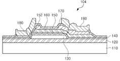
도 7, 도 8, 및 도 9를 참조하여 또 다른 실시 예에 따른 음향 공진기(104)를 설명한다.An
본 실시 예에 따른 음향 공진기(104)는 제1압전부(162)와 제2압전부(164) 간의 크기관계에 있어서 전술된 실시 예들과 구별된다.
The
제2압전부(164)는 제1압전부(162)보다 대체로 두껍게 형성될 수 있다. 예를 들어, 제2압전부(164)의 최저두께(Tm2)는 제1압전부(162)의 최저두께(Tm1)보다 크고, 제2압전부(164)의 최고두께(Tx2)는 제1압전부(162)의 최고두께(Tx1)보다 클 수 있다. 아울러, 제2압전부(164)의 평균두께(Ta2)는 제1압전부(162)의 평균두께(Ta1)보다 크고, 제2압전부(164)의 최대두께편차(Td2)는 제1압전부(162)의 최대두께편차(Td1)보다 클 수 있다.
The second
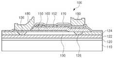
도 10, 도 11, 및 도 12를 참조하여 또 다른 실시 예에 따른 음향 공진기(106)를 설명한다.An
본 실시 예에 따른 음향 공진기(106)는 제1압전부(162)와 제2압전부(164) 간의 크기관계에 있어서 전술된 실시 예들과 구별된다.
The
예를 들어, 제2압전부(164)는 제1압전부(162)보다 대체로 두껍게 형성될 수 있다. 예를 들어, 제2압전부(164)의 최고두께(Tx2)는 제1압전부(162)의 최고두께(Tx1)보다 클 수 있다. 아울러, 제2압전부(164)의 최대두께편차(Td2)는 제1압전부(162)의 최대두께편차(Td1)보다 클 수 있다. 그러나 제2압전부(164)의 최저두께(Tm2)는 제1압전부(162)의 최저두께(Tm1)보다 작을 수 있다. 또한, 제2압전부(164)의 평균두께(Ta2)는 제1압전부(162)의 평균두께(Ta1)보다 작을 수 있다.
For example, the second
본 실시 예에 따른 음향 공진기(106)는 식각 저지층(122) 및 식각 저지부(126)의 구성에 있어서도 전술된 실시 예들과 구별된다.
The
예를 들어, 절연층(120) 상에는 식각 저지층(122)이 형성될 수 있다. 식각 저지층(122)은 식각 공정 단계에서 기판(110) 및 절연층(120) 등을 보호하는 구실을 할 수 있다. 식각 저지층(122)에는 식각 저지부(126), 공동(130) 및 희생층 패턴(124)이 형성될 수 있다. 식각 저지부(126), 공동(130) 및 희생층 패턴(124)은 실질적으로 동일한 높이로 형성될 수 있다. 따라서, 본 실시 예의 음향 공진기(106)는 박형화 및 단차 제거가 가능할 수 있다.
For example, an
공동(130)은 제1전극층(150), 압전층(160) 및 제2전극층(152)으로 구성되는 공진부가 소정 방향으로 진동할 수 있도록 제1전극층(150)의 하부에 위치한다. 공동(130)은 식각 저지층(122) 상에 희생층을 형성하고, 희생층 상에 제1전극층(150), 압전층(160) 및 제2전극층(152) 등을 적층한 후에 희생층을 에칭하여 제거하는 식각 공정에 의해 형성될 수 있다.
The
공동(130)의 외측에는 식각 저지부(126)가 형성될 수 있다. 식각 저지부(126)는 식각 저지층(122)에 돌기 형태로 형성된다. 공동(130)의 외주 경계면은 식각 저지부(126)에 의해 한정될 수 있다. 본 실시 형태의 경우, 식각 저지부(126)의 단면은 대략 상하 반전된 사다리꼴 형상일 수 있다. 식각 저지층(122) 및 식각 저지부(126)는 희생층을 제거하기 위한 식각 공정에서 식각되지 않는 물질로 형성될 수 있다. 일 예로, 식각 저지층(122) 및 식각 저지부(126)는 동일한 재료로 형성될 수 있다. 희생층이 제거된 후의 공동(130)의 형상은 식각 저지층(122) 및 식각 저지부(126)에 의해 둘러싸지는 공간에 의해 정의될 수 있다. 부연 설명하면, 공동(130)의 하부 경계면은 식각 저지층(122)에 의해 정의될 수 있고, 공동(130)의 외주 경계면은 식각 저지부(1226)에 의해 정의될 수 있다.
An etch stop 126 may be formed on the outside of the
식각 저지부(126)의 바깥쪽에는 희생층 패턴(124)이 형성될 수 있다. 희생층 패턴(124)은 식각 저지부(126)의 외측으로 연장되어 형성될 수 있다. 희생층 패턴(124)은 식각 저지층(122) 상에 형성되는 희생층 중 식각 공정 이후에 잔존하는 일 부분에 대응할 수 있다.
A
도 13을 참조하면, 본 발명의 일 실시 예에 따른 필터(200)는 래더 타입(ladder type)의 필터 구조로 형성될 수 있다. 예를 들어, 필터(200)는 복수의 음향 공진기(100)를 포함한다. 여기서, 하나의 음향 공진기(100)는 입력 신호(RFin)가 입력되는 신호 입력단과 출력 신호(RFout)가 출력되는 신호 출력단 사이에 직렬로 연결되고, 다른 하나의 음향 공진기(100)는 상기 신호 출력단과 접지 사이에 연결된다.
Referring to FIG. 13, the
본 발명은 이상에서 설명되는 실시 예에만 한정되는 것은 아니며, 본 발명이 속하는 기술분야에서 통상의 지식을 가진 자라면 이하의 특허청구범위에 기재된 본 발명의 기술적 사상의 요지를 벗어나지 않는 범위에서 얼마든지 다양하게 변경하여 실시할 수 있을 것이다. 예를 들어, 전술된 실시형태에 기재된 다양한 특징사항은 그와 반대되는 설명이 명시적으로 기재되지 않는 한 다른 실시형태에 결합하여 적용될 수 있다.
It will be apparent to those skilled in the art that various modifications and variations can be made in the present invention without departing from the spirit or scope of the inventions And various modifications may be made. For example, various features described in the foregoing embodiments can be applied in combination with other embodiments unless the description to the contrary is explicitly stated.
100음향 공진기
110기판
120절연층
130공동
140멤브레인층
150제1전극층
152제2전극층
160압전층
162제1압전부
164제2압전부
166제3압전부
170보호층
180제1접속 전극층
190제2접속 전극층
200필터
Ta1, Ta2(압전부의) 평균두께
Tm1, Tm2(압전부의) 최저두께
Tx1, Tx2(압전부의) 최고두께
Td1, Td2(압전부의) 최대두께편차100 acoustic resonator
110 substrate
120 insulating layer
130 joint
140 membrane layer
150 first electrode layer
152 Second electrode layer
160 piezoelectric layer
162 < tb >
164 < tb >
166 3rd full pressure
170 protective layer
180 first connection electrode layer
190 second connection electrode layer
200 filters
Ta1, Ta2 (in piezoelectric portion) average thickness
Tm1, Tm2 (of piezoelectric part) minimum thickness
Tx1, Tx2 (of piezoelectric part) maximum thickness
Td1, Td2 Maximum thickness deviation (of the piezoelectric part)
Claims (16)
Translated fromKorean상기 제1압전부의 가장자리에 배치되고 제2평균 두께를 갖는 제2압전부;
를 포함하고,
상기 제2압전부의 최대 두께 편차는 상기 제2압전부의 폭보다 작도록 구성되는 음향 공진기.A first piezoelectric portion disposed in the cavity and having a first average thickness; And
A second piezoelectric portion disposed at an edge of the first piezoelectric portion and having a second average thickness;
Lt; / RTI >
And the maximum thickness deviation of the second piezoelectric portion is smaller than the width of the second piezoelectric portion.
상기 제1평균 두께는 상기 제2평균 두께와 다르도록 구성되는 음향 공진기.The method according to claim 1,
Wherein the first average thickness is different from the second average thickness.
상기 제1압전부의 최저 두께는 상기 제2압전부의 최저 두께보다 크도록 구성되는 음향 공진기.The method according to claim 1,
Wherein the minimum thickness of the first piezoelectric portion is larger than the minimum thickness of the second piezoelectric portion.
상기 제1압전부의 최저 두께는 상기 제2압전부의 최저 두께보다 작도록 구성되는 음향 공진기.The method according to claim 1,
And the minimum thickness of the first piezoelectric portion is smaller than the minimum thickness of the second piezoelectric portion.
상기 제1압전부의 최고 두께는 상기 제2압전부의 최고 두께보다 작도록 구성되는 음향 공진기.The method according to claim 1,
And the maximum thickness of the first piezoelectric portion is smaller than the maximum thickness of the second piezoelectric portion.
상기 제1압전부 및 상기 제2압전부의 상부 및 하부에 각각 형성되는 전극층을 포함하는 음향 공진기.The method according to claim 1,
And an electrode layer formed on upper and lower portions of the first piezoelectric portion and the second piezoelectric portion, respectively.
상기 제2압전부의 가장자리에 배치되는 제3압전부를 포함하는 음향 공진기.The method according to claim 1,
And a third piezoelectric portion disposed at an edge of the second piezoelectric portion.
상기 제3압전부의 폭은 상기 제2압전부의 폭과 같거나 작도록 구성되는 음향 공진기.9. The method of claim 8,
And the width of the third piezoelectric portion is equal to or smaller than the width of the second piezoelectric portion.
상기 제1압전부의 가장자리에 배치되고, 제2최대두께편차를 갖는 제2압전부;
를 포함하는 음향 공진기.A first piezoelectric portion having a first maximum thickness deviation; And
A second piezoelectric portion disposed at an edge of the first piezoelectric portion and having a second maximum thickness deviation;
/ RTI >
상기 제2최대두께편차는 상기 제1최대두께편차보다 큰 음향 공진기.11. The method of claim 10,
Wherein the second maximum thickness deviation is greater than the first maximum thickness deviation.
상기 제1압전부의 평균두께는 상기 제2압전부의 평균두께와 다르게 구성되는 음향 공진기.11. The method of claim 10,
Wherein an average thickness of the first piezoelectric portion is different from an average thickness of the second piezoelectric portion.
상기 제1압전부의 최고 두께는 상기 제2압전부의 최고 두께보다 크지 않도록 구성되는 음향 공진기.11. The method of claim 10,
And the maximum thickness of the first piezoelectric portion is not larger than the maximum thickness of the second piezoelectric portion.
상기 제1압전부의 제1면에 배치되는 제1전극층; 및
상기 제1압전부의 제2면에 배치되는 제2전극층;
을 포함하는 음향 공진기.11. The method of claim 10,
A first electrode layer disposed on a first surface of the first piezoelectric portion; And
A second electrode layer disposed on a second surface of the first piezoelectric portion;
/ RTI >
상기 제1압전부와 기판 사이에 배치되는 공동을 포함하는 음향 공진기.11. The method of claim 10,
And a cavity disposed between the first piezoelectric portion and the substrate.
Priority Applications (4)
| Application Number | Priority Date | Filing Date | Title |
|---|---|---|---|
| KR1020160120664AKR101867285B1 (en) | 2016-09-21 | 2016-09-21 | Acoustic Wave Resonator And Filter including the Same |
| US15/459,756US10630258B2 (en) | 2016-09-21 | 2017-03-15 | Acoustic wave resonator and filter including the same |
| CN201710342931.3ACN107863948B (en) | 2016-09-21 | 2017-05-16 | Acoustic resonator and filter including the same |
| KR1020180060944AKR102426208B1 (en) | 2016-09-21 | 2018-05-29 | Acoustic Wave Resonator And Filter including the Same |
Applications Claiming Priority (1)
| Application Number | Priority Date | Filing Date | Title |
|---|---|---|---|
| KR1020160120664AKR101867285B1 (en) | 2016-09-21 | 2016-09-21 | Acoustic Wave Resonator And Filter including the Same |
Related Child Applications (1)
| Application Number | Title | Priority Date | Filing Date |
|---|---|---|---|
| KR1020180060944ADivisionKR102426208B1 (en) | 2016-09-21 | 2018-05-29 | Acoustic Wave Resonator And Filter including the Same |
Publications (2)
| Publication Number | Publication Date |
|---|---|
| KR20180032027A KR20180032027A (en) | 2018-03-29 |
| KR101867285B1true KR101867285B1 (en) | 2018-07-19 |
Family
ID=61621463
Family Applications (1)
| Application Number | Title | Priority Date | Filing Date |
|---|---|---|---|
| KR1020160120664AActiveKR101867285B1 (en) | 2016-09-21 | 2016-09-21 | Acoustic Wave Resonator And Filter including the Same |
Country Status (3)
| Country | Link |
|---|---|
| US (1) | US10630258B2 (en) |
| KR (1) | KR101867285B1 (en) |
| CN (1) | CN107863948B (en) |
Families Citing this family (11)
| Publication number | Priority date | Publication date | Assignee | Title |
|---|---|---|---|---|
| DE102018107496B3 (en)* | 2018-03-28 | 2019-07-11 | RF360 Europe GmbH | Volumetric wave resonator device and method for its production |
| CN111193484A (en)* | 2018-11-14 | 2020-05-22 | 天津大学 | Bulk acoustic wave resonator with rough surface, filter, and electronic device |
| CN111193485B (en)* | 2018-11-14 | 2023-10-27 | 天津大学 | Bulk acoustic resonator with roughened surface, filter, and electronic device |
| CN110868169B (en)* | 2019-01-28 | 2025-05-13 | 中国电子科技集团公司第十三研究所 | Resonators and semiconductor devices |
| CN110868175B (en)* | 2019-04-23 | 2023-06-27 | 中国电子科技集团公司第十三研究所 | Resonator with seed layer, filter and resonator preparation method |
| CN111010103A (en)* | 2019-05-31 | 2020-04-14 | 天津大学 | Resonator with multi-layer protrusion structure and its manufacturing method, filter and electronic device |
| KR102754241B1 (en)* | 2020-04-22 | 2025-01-14 | 가부시키가이샤 무라타 세이사쿠쇼 | Piezoelectric device |
| CN111865258B (en)* | 2020-08-10 | 2022-04-05 | 杭州星阖科技有限公司 | Manufacturing process of acoustic wave resonator and acoustic wave resonator |
| KR102609164B1 (en)* | 2021-01-25 | 2023-12-05 | 삼성전기주식회사 | Bulk acoustic resonator |
| CN113364423B (en)* | 2021-05-27 | 2023-11-10 | 广州乐仪投资有限公司 | Piezoelectric MEMS resonator, forming method thereof and electronic equipment |
| CN113992180B (en)* | 2021-12-27 | 2022-04-26 | 常州承芯半导体有限公司 | Bulk acoustic wave resonator device, forming method thereof, filter device and radio frequency front end device |
Citations (9)
| Publication number | Priority date | Publication date | Assignee | Title |
|---|---|---|---|---|
| KR100631217B1 (en)* | 2005-07-27 | 2006-10-04 | 삼성전자주식회사 | Integrated filter integrated with thin film bulk acoustic resonator and surface acoustic wave resonator and its manufacturing method |
| KR20100077346A (en)* | 2008-12-29 | 2010-07-08 | 주식회사 엠에스솔루션 | Film bulk acoustic resonator and method of manufacture |
| KR20120084295A (en)* | 2009-10-09 | 2012-07-27 | 꼼미사리아 아 레네르지 아토미끄 에뜨 옥스 에너지스 앨터네이티브즈 | Acoustic wave device including a surface wave filter and a bulk wave filter, and method for making same |
| KR20130044905A (en)* | 2011-10-25 | 2013-05-03 | 삼성전자주식회사 | Film bulk acoustic resonator and fabrication method thereof |
| KR20140043457A (en)* | 2012-08-17 | 2014-04-09 | 엔지케이 인슐레이터 엘티디 | Composite substrate, surface acoustic wave device, and method for manufacturing composite substrate |
| JP2015115870A (en)* | 2013-12-13 | 2015-06-22 | 株式会社村田製作所 | Acoustic wave device |
| KR20160015628A (en)* | 2014-07-31 | 2016-02-15 | 삼성전기주식회사 | Acoustic resonator and manufacturing method of the acoustic resonator |
| KR20160069263A (en)* | 2014-12-08 | 2016-06-16 | 삼성전기주식회사 | Acoustic resonator and manufacturing method thereof |
| KR20160069377A (en)* | 2014-12-08 | 2016-06-16 | 삼성전기주식회사 | Bulk acoustic wave resonator and filter |
Family Cites Families (9)
| Publication number | Priority date | Publication date | Assignee | Title |
|---|---|---|---|---|
| KR100576249B1 (en) | 2001-04-27 | 2006-05-03 | 서울전자통신(주) | Surface Acoustic Wave Filter Using Diamond Thin Film and Manufacturing Method Thereof |
| JP3760378B2 (en) | 2001-09-14 | 2006-03-29 | 株式会社村田製作所 | End-reflection type surface acoustic wave device and manufacturing method thereof |
| KR100616508B1 (en)* | 2002-04-11 | 2006-08-29 | 삼성전기주식회사 | FARA element and its manufacturing method |
| JP4435049B2 (en)* | 2005-08-08 | 2010-03-17 | 株式会社東芝 | Thin film piezoelectric resonator and manufacturing method thereof |
| KR100802109B1 (en) | 2006-09-12 | 2008-02-11 | 삼성전자주식회사 | Resonator, apparatus having same and manufacturing method of resonator |
| JP4838093B2 (en)* | 2006-10-25 | 2011-12-14 | 太陽誘電株式会社 | Piezoelectric thin film resonator and filter |
| FR2947398B1 (en)* | 2009-06-30 | 2013-07-05 | Commissariat Energie Atomique | DEVICE RESONANT TO GUIDED ACOUSTIC WAVES AND METHOD OF MAKING THE DEVICE |
| JP6371518B2 (en)* | 2013-12-17 | 2018-08-08 | 太陽誘電株式会社 | Piezoelectric thin film resonator, method for manufacturing the same, filter, and duplexer |
| US10700665B2 (en)* | 2015-12-04 | 2020-06-30 | Intel Corporation | Film bulk acoustic resonator (FBAR) devices for high frequency RF filters |
- 2016
- 2016-09-21KRKR1020160120664Apatent/KR101867285B1/enactiveActive
- 2017
- 2017-03-15USUS15/459,756patent/US10630258B2/enactiveActive
- 2017-05-16CNCN201710342931.3Apatent/CN107863948B/enactiveActive
Patent Citations (9)
| Publication number | Priority date | Publication date | Assignee | Title |
|---|---|---|---|---|
| KR100631217B1 (en)* | 2005-07-27 | 2006-10-04 | 삼성전자주식회사 | Integrated filter integrated with thin film bulk acoustic resonator and surface acoustic wave resonator and its manufacturing method |
| KR20100077346A (en)* | 2008-12-29 | 2010-07-08 | 주식회사 엠에스솔루션 | Film bulk acoustic resonator and method of manufacture |
| KR20120084295A (en)* | 2009-10-09 | 2012-07-27 | 꼼미사리아 아 레네르지 아토미끄 에뜨 옥스 에너지스 앨터네이티브즈 | Acoustic wave device including a surface wave filter and a bulk wave filter, and method for making same |
| KR20130044905A (en)* | 2011-10-25 | 2013-05-03 | 삼성전자주식회사 | Film bulk acoustic resonator and fabrication method thereof |
| KR20140043457A (en)* | 2012-08-17 | 2014-04-09 | 엔지케이 인슐레이터 엘티디 | Composite substrate, surface acoustic wave device, and method for manufacturing composite substrate |
| JP2015115870A (en)* | 2013-12-13 | 2015-06-22 | 株式会社村田製作所 | Acoustic wave device |
| KR20160015628A (en)* | 2014-07-31 | 2016-02-15 | 삼성전기주식회사 | Acoustic resonator and manufacturing method of the acoustic resonator |
| KR20160069263A (en)* | 2014-12-08 | 2016-06-16 | 삼성전기주식회사 | Acoustic resonator and manufacturing method thereof |
| KR20160069377A (en)* | 2014-12-08 | 2016-06-16 | 삼성전기주식회사 | Bulk acoustic wave resonator and filter |
Also Published As
| Publication number | Publication date |
|---|---|
| US20180083597A1 (en) | 2018-03-22 |
| CN107863948B (en) | 2021-07-13 |
| CN107863948A (en) | 2018-03-30 |
| US10630258B2 (en) | 2020-04-21 |
| KR20180032027A (en) | 2018-03-29 |
Similar Documents
| Publication | Publication Date | Title |
|---|---|---|
| KR101867285B1 (en) | Acoustic Wave Resonator And Filter including the Same | |
| KR102248528B1 (en) | Acoustic resonator and method of manufacturing thereof | |
| KR101973416B1 (en) | Acoustic resonator and manufacturing method of the acoustic resonator | |
| JP6336712B2 (en) | Piezoelectric thin film resonator, filter and duplexer | |
| US10897002B2 (en) | Acoustic resonator and method of manufacturing the same | |
| KR101901696B1 (en) | Bulk acoustic wave resonator and filter including the same | |
| CN109818591B (en) | Acoustic wave resonator | |
| KR20170130228A (en) | Acoustic resonator and method of manufacturing thereof | |
| KR20160086552A (en) | Acoustic resonator and manufacturing method thereof | |
| JP2017225042A (en) | Piezoelectric thin film resonator, filter, and multiplexer | |
| JP2015119249A (en) | Piezoelectric thin film resonator, method for manufacturing the same, filter, and duplexer | |
| US9787282B2 (en) | Piezoelectric thin film resonator, filter and duplexer | |
| JP6469601B2 (en) | Piezoelectric thin film resonator, filter and duplexer | |
| KR20170122539A (en) | Bulk acoustic wave resonator and method for manufacturing the same | |
| JP6423782B2 (en) | Piezoelectric thin film resonator and filter | |
| KR102145309B1 (en) | Acoustic resonator | |
| KR20180131313A (en) | Acoustic resonator and method for fabricating the same | |
| KR102172638B1 (en) | Acoustic resonator and method of manufacturing thereof | |
| KR102426208B1 (en) | Acoustic Wave Resonator And Filter including the Same | |
| KR20200076555A (en) | Acoustic resonator | |
| CN111342802B (en) | Acoustic wave resonator | |
| US20230087049A1 (en) | Bulk acoustic resonator | |
| CN118868847A (en) | Bulk Acoustic Wave Resonator | |
| KR20240136097A (en) | Bulk acoustic resonator filter | |
| KR20240158631A (en) | Bulk acoustic resonator, bulk acoustic resonator filter, and manufacturing metho thereof |
Legal Events
| Date | Code | Title | Description |
|---|---|---|---|
| A201 | Request for examination | ||
| PA0109 | Patent application | Patent event code:PA01091R01D Comment text:Patent Application Patent event date:20160921 | |
| PA0201 | Request for examination | ||
| E902 | Notification of reason for refusal | ||
| PE0902 | Notice of grounds for rejection | Comment text:Notification of reason for refusal Patent event date:20170919 Patent event code:PE09021S01D | |
| E701 | Decision to grant or registration of patent right | ||
| PE0701 | Decision of registration | Patent event code:PE07011S01D Comment text:Decision to Grant Registration Patent event date:20180307 | |
| PG1501 | Laying open of application | ||
| PA0107 | Divisional application | Comment text:Divisional Application of Patent Patent event date:20180529 Patent event code:PA01071R01D | |
| PR0701 | Registration of establishment | Comment text:Registration of Establishment Patent event date:20180607 Patent event code:PR07011E01D | |
| PR1002 | Payment of registration fee | Payment date:20180608 End annual number:3 Start annual number:1 | |
| PG1601 | Publication of registration | ||
| PR1001 | Payment of annual fee | Payment date:20210413 Start annual number:4 End annual number:4 | |
| PR1001 | Payment of annual fee | Payment date:20211221 Start annual number:5 End annual number:5 | |
| PR1001 | Payment of annual fee | Payment date:20240528 Start annual number:7 End annual number:7 | |
| PR1001 | Payment of annual fee | Payment date:20250526 Start annual number:8 End annual number:8 |