KR101865305B1 - Touch detection chip and touch input device - Google Patents
Touch detection chip and touch input deviceDownload PDFInfo
- Publication number
- KR101865305B1 KR101865305B1KR1020170097543AKR20170097543AKR101865305B1KR 101865305 B1KR101865305 B1KR 101865305B1KR 1020170097543 AKR1020170097543 AKR 1020170097543AKR 20170097543 AKR20170097543 AKR 20170097543AKR 101865305 B1KR101865305 B1KR 101865305B1
- Authority
- KR
- South Korea
- Prior art keywords
- driving
- pressure
- electrodes
- touch
- sensing
- Prior art date
- Legal status (The legal status is an assumption and is not a legal conclusion. Google has not performed a legal analysis and makes no representation as to the accuracy of the status listed.)
- Active
Links
Images


Classifications
- G—PHYSICS
- G06—COMPUTING OR CALCULATING; COUNTING
- G06F—ELECTRIC DIGITAL DATA PROCESSING
- G06F3/00—Input arrangements for transferring data to be processed into a form capable of being handled by the computer; Output arrangements for transferring data from processing unit to output unit, e.g. interface arrangements
- G06F3/01—Input arrangements or combined input and output arrangements for interaction between user and computer
- G06F3/03—Arrangements for converting the position or the displacement of a member into a coded form
- G06F3/041—Digitisers, e.g. for touch screens or touch pads, characterised by the transducing means
- G06F3/0416—Control or interface arrangements specially adapted for digitisers
- G—PHYSICS
- G06—COMPUTING OR CALCULATING; COUNTING
- G06F—ELECTRIC DIGITAL DATA PROCESSING
- G06F3/00—Input arrangements for transferring data to be processed into a form capable of being handled by the computer; Output arrangements for transferring data from processing unit to output unit, e.g. interface arrangements
- G06F3/01—Input arrangements or combined input and output arrangements for interaction between user and computer
- G06F3/03—Arrangements for converting the position or the displacement of a member into a coded form
- G06F3/041—Digitisers, e.g. for touch screens or touch pads, characterised by the transducing means
- G06F3/0412—Digitisers structurally integrated in a display
- G—PHYSICS
- G06—COMPUTING OR CALCULATING; COUNTING
- G06F—ELECTRIC DIGITAL DATA PROCESSING
- G06F3/00—Input arrangements for transferring data to be processed into a form capable of being handled by the computer; Output arrangements for transferring data from processing unit to output unit, e.g. interface arrangements
- G06F3/01—Input arrangements or combined input and output arrangements for interaction between user and computer
- G06F3/03—Arrangements for converting the position or the displacement of a member into a coded form
- G06F3/041—Digitisers, e.g. for touch screens or touch pads, characterised by the transducing means
- G06F3/0414—Digitisers, e.g. for touch screens or touch pads, characterised by the transducing means using force sensing means to determine a position
- G—PHYSICS
- G06—COMPUTING OR CALCULATING; COUNTING
- G06F—ELECTRIC DIGITAL DATA PROCESSING
- G06F3/00—Input arrangements for transferring data to be processed into a form capable of being handled by the computer; Output arrangements for transferring data from processing unit to output unit, e.g. interface arrangements
- G06F3/01—Input arrangements or combined input and output arrangements for interaction between user and computer
- G06F3/03—Arrangements for converting the position or the displacement of a member into a coded form
- G06F3/041—Digitisers, e.g. for touch screens or touch pads, characterised by the transducing means
- G06F3/044—Digitisers, e.g. for touch screens or touch pads, characterised by the transducing means by capacitive means
- G—PHYSICS
- G09—EDUCATION; CRYPTOGRAPHY; DISPLAY; ADVERTISING; SEALS
- G09G—ARRANGEMENTS OR CIRCUITS FOR CONTROL OF INDICATING DEVICES USING STATIC MEANS TO PRESENT VARIABLE INFORMATION
- G09G3/00—Control arrangements or circuits, of interest only in connection with visual indicators other than cathode-ray tubes
- G09G3/20—Control arrangements or circuits, of interest only in connection with visual indicators other than cathode-ray tubes for presentation of an assembly of a number of characters, e.g. a page, by composing the assembly by combination of individual elements arranged in a matrix no fixed position being assigned to or needed to be assigned to the individual characters or partial characters
Landscapes
- Engineering & Computer Science (AREA)
- Theoretical Computer Science (AREA)
- General Engineering & Computer Science (AREA)
- Physics & Mathematics (AREA)
- General Physics & Mathematics (AREA)
- Human Computer Interaction (AREA)
- Computer Hardware Design (AREA)
- Position Input By Displaying (AREA)
Abstract
Translated fromKoreanDescription
Translated fromKorean본 발명은 터치 검출기, 터치 검출 칩 및 터치 입력 장치에 관한 것으로, 보다 상세하게는 터치 위치 및 터치 압력을 검출할 수 있도록 하는 터치 검출기, 터치 검출 칩 및 이를 포함하는 터치 입력 장치에 관한 것이다.The present invention relates to a touch detector, a touch detection chip, and a touch input device, and more particularly, to a touch detector, a touch detection chip, and a touch input device that can detect a touch position and a touch pressure.
컴퓨팅 시스템의 조작을 위해 다양한 종류의 입력 장치들이 이용되고 있다. 예컨대, 버튼(button), 키(key), 조이스틱(joystick) 및 터치 스크린과 같은 입력 장치가 이용되고 있다. 터치 스크린의 쉽고 간편한 조작으로 인해 컴퓨팅 시스템의 조작시 터치 스크린의 이용이 증가하고 있다.Various types of input devices are used for the operation of the computing system. For example, an input device such as a button, a key, a joystick, and a touch screen is used. Due to the easy and simple operation of the touch screen, the use of the touch screen in the operation of the computing system is increasing.
터치 스크린은, 터치-감응 표면(touch-sensitive surface)을 구비한 투명한 패널일 수 있는 터치 센서 패널(touch sensor panel)을 포함하는 터치 입력 장치의 터치 표면을 구성할 수 있다. 이러한 터치 센서 패널은 디스플레이 스크린의 전면에 부착되어 터치-감응 표면이 디스플레이 스크린의 보이는 면을 덮을 수 있다. 사용자가 손가락 등으로 터치 스크린을 단순히 터치함으로써 사용자가 컴퓨팅 시스템을 조작할 수 있도록 한다. 일반적으로, 컴퓨팅 시스템은 터치 스크린상의 터치 및 터치 위치를 인식하고 이러한 터치를 해석함으로써 이에 따라 연산을 수행할 수 있다.The touch screen may comprise a touch surface of a touch input device including a touch sensor panel, which may be a transparent panel having a touch-sensitive surface. Such a touch sensor panel may be attached to the front of the display screen such that the touch-sensitive surface covers the visible surface of the display screen. The user simply touches the touch screen with a finger or the like so that the user can operate the computing system. Generally, a computing system is able to recognize touch and touch locations on a touch screen and interpret the touch to perform operations accordingly.
이와 더불어, 터치 입력 장치의 터치 표면에 대한 터치 위치뿐 아니라 터치 압력을 검출하기 위한 연구가 지속되고 있다. 이때, 터치 센서 패널에 대한 터치 위치를 검출하는 구성과 압력 전극으로부터 터치 압력을 검출하는 구성이 별도로 제작되어야 하므로 비용이 증가할 뿐 아니라 공정이 복잡하고, 또한 이들 구성이 터치 입력 장치에서 차지하는 부피 및 면적 소모가 커지는 문제점이 발생한다.In addition, studies for detecting the touch position as well as the touch pressure on the touch surface of the touch input device are continuing. At this time, since the configuration for detecting the touch position with respect to the touch sensor panel and the structure for detecting the touch pressure from the pressure electrode must be separately manufactured, the cost is increased and the process is complicated. Further, There arises a problem that the area consumption is increased.
본 발명의 목적은 전술한 문제점을 해소하기 위한 것으로 터치 센서 패널에 대한 터치 위치 및 압력 전극으로 터치 압력을 하나의 구성에서 검출할 수 있도록 하는 터치 검출기, 터치 검출 칩 및 터치 입력 장치를 제공하는 것이다.SUMMARY OF THE INVENTION It is an object of the present invention to provide a touch detector, a touch detection chip and a touch input device for detecting a touch pressure on a touch position and a pressure electrode on a touch sensor panel, .
본 발명의 또 다른 목적은 애플리케이션에 무관하게 터치 검출기 및 터치 검출 칩에 대한 수정 없이 간단히 압력 크기를 검출할 수 있도록 하는 기술을 제공하는 것이다.It is still another object of the present invention to provide a technique for easily detecting a pressure magnitude without modification to a touch detector and a touch detection chip regardless of an application.
본 발명에 따른 터치 검출 칩은 복수의 전극 중 적어도 2개 이상의 전극에 구동신호를 인가할 수 있도록 구성된 구동부; 상기 복수의 전극 중 적어도 2개 이상의 전극으로부터 복수의 신호를 수신하여 터치 위치 및 터치 압력을 검출할 수 있도록 구성된 감지부; 및 상기 구동신호를 전달하기 위한 복수의 출력단자를 포함하며, 상기 복수의 출력단자 중 적어도 하나는 압력 검출만을 위한 압력 검출용 출력단자이고, 상기 구동신호가 인가되는 상기 적어도 2개 이상의 전극은 적어도 하나의 압력 검출용 구동전극과 n개의 위치 검출용 구동전극을 포함하고, 상기 구동부는, 제1시간구간에 상기 n개의 위치 검출용 구동전극에 구동신호를 인가하고 상기 제1시간구간과 다른 제2시간구간에 상기 적어도 하나의 압력 검출용 구동전극에 구동신호를 인가하도록 구성되고, n은 자연수일 수 있다.A touch detection chip according to the present invention includes: a driving unit configured to apply a driving signal to at least two electrodes among a plurality of electrodes; A sensing unit configured to receive a plurality of signals from at least two or more of the plurality of electrodes and detect a touch position and a touch pressure; And at least one of the plurality of output terminals is a pressure detection output terminal for pressure detection only, and the at least two electrodes to which the drive signal is applied are at least Wherein the drive unit applies a drive signal to the n number of position detection drive electrodes in a first time interval and outputs the drive signal to the n number of position detection drive electrodes, And a driving signal is applied to the at least one driving electrode for pressure detection in a 2-hour period, and n may be a natural number.
본 발명에 따른 다른 터치 검출칩은 복수의 전극 중 적어도 2개 이상의 전극에 구동신호를 인가할 수 있도록 구성된 구동부; 상기 복수의 전극 중 적어도 2개 이상의 전극으로부터 복수의 신호를 수신하여 터치 위치 및 터치 압력을 검출할 수 있도록 구성된 감지부; 및 상기 구동신호를 전달하기 위한 복수의 출력단자를 포함하며, 상기 복수의 출력 단자 중 적어도 하나는 압력 검출만을 위한 압력 검출용 출력단자이고, 상기 구동신호가 인가되는 상기 적어도 2개 이상의 전극은 적어도 하나의 압력 검출용 구동전극과 n개의 위치 검출용 구동전극을 포함하고, 상기 구동부는, 상기 n개의 위치 검출용 구동전극에 구동신호를 인가하는 시간구간 동안에 상기 적어도 하나의 압력 검출용 구동전극에 구동신호를 인가하도록 구성되고, n은 자연수일 수 있다.Another touch detection chip according to the present invention includes: a driver configured to apply a driving signal to at least two electrodes among a plurality of electrodes; A sensing unit configured to receive a plurality of signals from at least two or more of the plurality of electrodes and detect a touch position and a touch pressure; And at least one of the plurality of output terminals is a pressure detection output terminal for pressure detection only, and the at least two electrodes to which the drive signal is applied are at least Wherein the driving unit includes a driving electrode for pressure detection and n driving electrodes for position detection, and the driving unit applies driving signals to the at least one driving electrode for pressure detection during a time interval for applying driving signals to the n- And to apply a driving signal, and n may be a natural number.
본 발명에 따른 터치 입력 장치는 복수의 전극; 및 터치 검출 칩을 포함하며, 상기 터치 검출 칩은: 복수의 전극 중 적어도 2개 이상의 전극에 구동신호를 인가할 수 있도록 구성된 구동부; 상기 복수의 전극 중 적어도 2개 이상의 전극으로부터 복수의 신호를 수신하여 터치 위치 및 터치 압력을 검출할 수 있도록 구성된 감지부; 및 상기 구동신호를 전달하기 위한 복수의 출력단자를 포함하며, 상기 복수의 출력단자 중 적어도 하나는 압력 검출만을 위한 압력 검출용 출력단자이고, 상기 구동신호가 인가되는 상기 적어도 2개 이상의 전극은 적어도 하나의 압력 검출용 구동전극과 n개의 위치 검출용 구동전극을 포함하고, 상기 구동부는, 제1시간구간에 상기 n개의 위치 검출용 구동전극에 구동신호를 인가하고 상기 제1시간구간과 다른 제2시간구간에 상기 적어도 하나의 압력 검출용 구동전극에 구동신호를 인가하도록 구성되고, n은 자연수일 수 있다.A touch input device according to the present invention includes: a plurality of electrodes; And a touch detection chip, wherein the touch detection chip comprises: a driver configured to apply a driving signal to at least two electrodes among a plurality of electrodes; A sensing unit configured to receive a plurality of signals from at least two or more of the plurality of electrodes and detect a touch position and a touch pressure; And at least one of the plurality of output terminals is a pressure detection output terminal for pressure detection only, and the at least two electrodes to which the drive signal is applied are at least Wherein the drive unit applies a drive signal to the n number of position detection drive electrodes in a first time interval and outputs the drive signal to the n number of position detection drive electrodes, And a driving signal is applied to the at least one driving electrode for pressure detection in a 2-hour period, and n may be a natural number.
본 발명에 따른 다른 터치 입력 장치는 복수의 전극; 및 터치 검출 칩을 포함하며, 상기 터치 검출 칩은: 복수의 전극 중 적어도 2개 이상의 전극에 구동신호를 인가할 수 있도록 구성된 구동부; 상기 복수의 전극 중 적어도 2개 이상의 전극으로부터 복수의 신호를 수신하여 터치 위치 및 터치 압력을 검출할 수 있도록 구성된 감지부; 및 상기 구동신호를 전달하기 위한 복수의 출력단자를 포함하며, 상기 복수의 출력 단자 중 적어도 하나는 압력 검출만을 위한 압력 검출용 출력단자이고, 상기 구동신호가 인가되는 상기 적어도 2개 이상의 전극은 적어도 하나의 압력 검출용 구동전극과 n개의 위치 검출용 구동전극을 포함하고, 상기 구동부는, 상기 n개의 위치 검출용 구동전극에 구동신호를 인가하는 시간구간 동안에 상기 적어도 하나의 압력 검출용 구동전극에 구동신호를 인가하도록 구성되고, n은 자연수일 수 있다.Another touch input device according to the present invention includes a plurality of electrodes; And a touch detection chip, wherein the touch detection chip comprises: a driver configured to apply a driving signal to at least two electrodes among a plurality of electrodes; A sensing unit configured to receive a plurality of signals from at least two or more of the plurality of electrodes and detect a touch position and a touch pressure; And at least one of the plurality of output terminals is a pressure detection output terminal for pressure detection only, and the at least two electrodes to which the drive signal is applied are at least Wherein the driving unit includes a driving electrode for pressure detection and n driving electrodes for position detection, and the driving unit applies driving signals to the at least one driving electrode for pressure detection during a time interval for applying driving signals to the n- And to apply a driving signal, and n may be a natural number.
본 발명에 따르면 터치 센서 패널에 대한 터치 위치 및 압력 전극으로 터치 압력을 하나의 구성에서 검출할 수 있도록 하는 터치 검출기, 터치 검출 칩 및 터치 입력 장치를 제공할 수 있다.According to the present invention, it is possible to provide a touch detector, a touch detection chip, and a touch input device that can detect a touch pressure with a touch position and a pressure electrode with respect to a touch sensor panel in one configuration.
또한 본 발명에 따르면 애플리케이션에 무관하게 터치 검출기 및 터치 검출 칩에 대한 수정 없이 간단히 압력 크기를 검출할 수 있도록 하는 기술을 제공할 수 있다.Further, according to the present invention, it is possible to provide a technique for easily detecting the pressure magnitude without modification to the touch detector and the touch detection chip regardless of the application.
도1은 실시예에 따른 정전 용량 방식의 터치 센서 패널 및 이의 동작을 위한 구성의 개략도이다.
도2a, 도2b 및 도2c는 실시예에 따른 터치 입력 장치에서 디스플레이 모듈에 대한 터치 센서 패널의 상대적인 위치를 예시하는 개념도이다.
도3a는 실시예에 따른 압력 전극이 적용된 터치 입력 장치의 단면을 예시한다.
도3b는 실시예에 따른 압력 전극의 구조를 예시한다.
도4는 실시예에 따른 터치 검출기와 터치 센서 패널 및 압력 전극 사이의 신호 전달을 예시하는 개념도이다.
도5는 실시예에 따른 터치 검출 칩을 예시한다.
도6은 실시예에 따른 터치 입력 장치의 구동부, 감지부 및 전극부의 연결관계를 나타내는 등가 회로도를 예시한다.
도7은 실시예에 따른 터치 검출기의 구동부에서 전극부에 인가되는 구동신호를 예시한다.
도8a 내지 도8c는 각각, 실시예에 따른 터치 입력 장치에서 제1대체예의 압력 전극 및 감지부의 등가 회로도, 압력 전극 구조, 및 압력 전극과 기준 전위층 사이의 거리 변화에 따른 감지부의 출력신호를 나타내는 그래프이다.
도9는 실시예에 따른 터치 입력 장치에서 제2대체예의 압력 전극 및 감지부의 등가 회로도이다.1 is a schematic view of a touch sensor panel of a capacitive type according to an embodiment and a structure for its operation.
FIGS. 2A, 2B and 2C are conceptual diagrams illustrating the relative positions of the touch sensor panel with respect to the display module in the touch input device according to the embodiment.
3A illustrates a cross-section of a touch input device to which a pressure electrode according to an embodiment is applied.
3B illustrates the structure of a pressure electrode according to an embodiment.
4 is a conceptual diagram illustrating signal transmission between a touch detector, a touch sensor panel, and a pressure electrode according to an embodiment.
5 illustrates a touch detection chip according to an embodiment.
6 illustrates an equivalent circuit diagram illustrating a connection relationship between a driver, a sensing unit, and an electrode unit of the touch input device according to the embodiment.
7 illustrates a driving signal applied to the electrode unit in the driving unit of the touch detector according to the embodiment.
8A to 8C are diagrams showing equivalent circuit diagrams of the pressure electrode and sensing unit of the first alternative example, the pressure electrode structure, and the output signal of the sensing unit according to the change in distance between the pressure electrode and the reference potential layer in the touch input apparatus according to the embodiment FIG.
9 is an equivalent circuit diagram of the pressure electrode and sensing unit of the second alternative example in the touch input device according to the embodiment.
후술하는 본 발명에 대한 상세한 설명은, 본 발명이 실시될 수 있는 특정 실시예를 예시로서 도시하는 첨부 도면을 참조한다. 이들 실시예는 당업자가 본 발명을 실시할 수 있기에 충분하도록 상세히 설명된다. 본 발명의 다양한 실시예는 서로 다르지만 상호 배타적일 필요는 없음이 이해되어야 한다. 도면에서 유사한 참조부호는 여러 측면에 걸쳐서 동일하거나 유사한 기능을 지칭한다.The following detailed description of the invention refers to the accompanying drawings, which illustrate, by way of illustration, specific embodiments in which the invention may be practiced. These embodiments are described in sufficient detail to enable those skilled in the art to practice the invention. It should be understood that the various embodiments of the present invention are different, but need not be mutually exclusive. In the drawings, like reference numerals refer to the same or similar functions throughout the several views.
이하, 첨부되는 도면을 참조하여 본 발명의 실시예에 따른 터치 검출기, 터치 검출 칩 및 터치 입력 장치를 설명한다. 이하에서는 정전용량 방식의 터치 위치 및 압력 검출 방식이 설명되나 본 발명의 실시예에 개시된 사상의 범위 내라면 임의의 방식으로 터치 위치 및/또는 터치 압력을 검출할 수 있는 터치 검출기, 터치 검출 칩 및 터치 입력 장치가 본 발명의 범위에 포함될 수 있다.Hereinafter, a touch detector, a touch detection chip, and a touch input device according to embodiments of the present invention will be described with reference to the accompanying drawings. Although the touch position and the pressure detection method of the capacitive type are described below, the touch detector and the touch detection chip capable of detecting the touch position and / or the touch pressure in any manner within the range of the scope disclosed in the embodiments of the present invention, A touch input device may be included in the scope of the present invention.
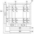
도1은 실시예에 따른 정전 용량 방식의 터치 센서 패널 및 이의 동작을 위한 구성의 개략도이다. 도1을 참조하면, 실시예에 따른 터치 센서 패널(100)은 복수의 구동전극(TX1 내지 TXn) 및 복수의 수신전극(RX1 내지 RXm)을 포함하며, 상기 터치 센서 패널(100)의 동작을 위해 복수의 구동전극(TX1 내지 TXn)에 구동신호를 인가하는 구동부(110), 및 터치 센서 패널(100)의 터치 표면에 대한 터치에 따라 변화되는 정전용량 변화량에 대한 정보를 포함하는 신호를 수신하여 터치 여부 및 터치 위치를 검출하는 감지부(120)를 포함할 수 있다.1 is a schematic view of a touch sensor panel of a capacitive type according to an embodiment and a configuration for its operation. 1, a
도1에 도시된 바와 같이, 터치 센서 패널(100)은 복수의 구동전극(TX1 내지 TXn)과 복수의 수신전극(RX1 내지 RXm)을 포함할 수 있다. 도1에서는 터치 센서 패널(100)의 복수의 구동전극(TX1 내지 TXn)과 복수의 수신전극(RX1 내지 RXm)이 직교 어레이를 구성하는 것으로 도시되어 있지만, 본 발명은 이에 한정되지 않으며, 복수의 구동전극(TX1 내지 TXn)과 복수의 수신전극(RX1 내지 RXm)이 대각선, 동심원 및 3차원 랜덤 배열 등을 비롯한 임의의 수의 차원 및 이의 응용 배열을 갖도록 할 수 있다. 여기서, n 및 m은 양의 정수로서 서로 같거나 다른 값을 가질 수 있으며 실시예에 따라 크기가 달라질 수 있다.As shown in FIG. 1, the
도1에 도시된 바와 같이, 복수의 구동전극(TX1 내지 TXn)과 복수의 수신전극(RX1 내지 RXm)은 각각 서로 교차하도록 배열될 수 있다. 구동전극(TX)은 제1축 방향으로 연장된 복수의 구동전극(TX1 내지 TXn)을 포함하고 수신전극(RX)은 제1축 방향과 교차하는 제2축 방향으로 연장된 복수의 수신전극(RX1 내지 RXm)을 포함할 수 있다.As shown in FIG. 1, the plurality of driving electrodes TX1 to TXn and the plurality of receiving electrodes RX1 to RXm may be arranged to cross each other. The driving electrode TX includes a plurality of driving electrodes TX1 to TXn extending in a first axis direction and a receiving electrode RX includes a plurality of receiving electrodes extending in a second axis direction intersecting the first axis direction RX1 to RXm).
본 발명의 실시예에 따른 터치 센서 패널(100)에서 복수의 구동전극(TX1 내지 TXn)과 복수의 수신전극(RX1 내지 RXm)은 서로 동일한 층에 형성될 수 있다. 예컨대, 복수의 구동전극(TX1 내지 TXn)과 복수의 수신전극(RX1 내지 RXm)은 절연막(미도시)의 동일한 면에 형성될 수 있다. 또한, 복수의 구동전극(TX1 내지 TXn)과 복수의 수신전극(RX1 내지 RXm)은 서로 다른 층에 형성될 수 있다. 예컨대, 복수의 구동전극(TX1 내지 TXn)과 복수의 수신전극(RX1 내지 RXm)은 하나의 절연막(미도시)의 양면에 각각 형성될 수도 있고, 또는 복수의 구동전극(TX1 내지 TXn)은 제1절연막(미도시)의 일면에 그리고 복수의 수신전극(RX1 내지 RXm)은 상기 제1절연막과 다른 제2절연막(미도시)의 일면상에 형성될 수 있다.In the
복수의 구동전극(TX1 내지 TXn)과 복수의 수신전극 (RX1 내지 RXm)은 투명 전도성 물질(예를 들면, 산화주석(SnO2) 및 산화인듐(In2O3) 등으로 이루어지는 ITO(Indium Tin Oxide) 또는 ATO(Antimony Tin Oxide)) 등으로 형성될 수 있다. 하지만, 이는 단지 예시일 뿐이며 구동전극(TX) 및 수신전극(RX)은 다른 투명 전도성 물질 또는 불투명 전도성 물질로 형성될 수도 있다. 예컨대, 구동전극(TX) 및 수신전극(RX)은 은잉크(silver ink), 구리(copper) 또는 탄소 나노튜브(CNT: Carbon Nanotube) 중 적어도 어느 하나를 포함하여 구성될 수 있다. 또한, 구동전극(TX) 및 수신전극(RX)는 메탈 메쉬(metal mesh)로 구현되거나 은나노(nano silver) 물질로 구성될 수 있다.A plurality of drive electrodes (TX1 to TXn) and a plurality of receiving electrodes (RX1 to RXm) is a transparent conductive material (e.g., tin oxide (SnO2) and indium oxide(In 2 O 3) ITO ( Indium Tin made of such Oxide) or ATO (antimony tin oxide)). However, this is merely an example, and the driving electrode TX and the receiving electrode RX may be formed of another transparent conductive material or an opaque conductive material. For example, the driving electrode TX and the receiving electrode RX may include at least one of silver ink, copper, or carbon nanotube (CNT). The driving electrode TX and the receiving electrode RX may be formed of a metal mesh or may be formed of a nano silver material.
실시예에 따른 구동부(110)는 구동신호를 구동전극(TX1 내지 TXn)에 인가할 수 있다. 실시예에서, 구동신호는 제1구동전극(TX1)부터 제n구동전극(TXn)까지 순차적으로 한번에 하나의 구동전극에 대해서 인가될 수 있다. 이러한 구동신호의 인가는 재차 반복적으로 이루어질 수 있다. 이는 단지 예시일 뿐이며, 실시예에 따라 다수의 구동전극에 구동신호가 동시에 인가될 수도 있다.The
감지부(120)는 수신전극(RX1 내지 RXm)을 통해 구동신호가 인가된 구동전극(TX1 내지 TXn)과 수신전극(RX1 내지 RXm) 사이에 생성된 정전용량(Cm: 101)에 관한 정보를 포함하는 감지신호를 수신함으로써 터치 여부 및 터치 위치를 검출할 수 있다. 예컨대, 감지신호는 구동전극(TX)에 인가된 구동신호가 구동전극(TX)과 수신전극(RX) 사이에 생성된 정전용량(CM: 101)에 의해 커플링된 신호일 수 있다. 이와 같이, 제1구동전극(TX1)부터 제n구동전극(TXn)까지 인가된 구동신호를 수신전극(RX1 내지 RXm)을 통해 감지하는 과정은 터치 센서 패널(100)을 스캔(scan)한다고 지칭할 수 있다. 감지부(120)의 구성 및 동작에 대해서는 도6을 참조하여 더욱 상세하게 설명된다.The
제어부(130)는 구동부(110)와 감지부(120)의 동작을 제어하는 기능을 수행할 수 있다. 예컨대, 제어부(130)는 구동제어신호를 생성한 후 구동부(120)에 전달하여 구동신호가 소정 시간에 미리 설정된 구동전극(TX)에 인가되도록 할 수 있다. 또한, 제어부(130)는 감지제어신호를 생성한 후 감지부(120)에 전달하여 감지부(120)가 소정 시간에 미리 설정된 수신전극(RX)으로부터 감지신호를 입력받아 미리 설정된 기능을 수행하도록 할 수 있다.The
이상에서 살펴본 바와 같이, 구동전극(TX)과 수신전극(RX)의 교차 지점마다 소정 값의 정전용량(C)이 생성되며, 손가락과 같은 객체가 터치 센서 패널(100)에 근접하는 경우 이러한 정전용량의 값이 변경될 수 있다. 도1에서 상기 정전용량은 상호 정전용량(Cm)을 나타낼 수 있다. 이러한 전기적 특성을 감지부(120)에서 감지하여 터치 센서 패널(100)에 대한 터치 여부 및/또는 터치 위치를 감지할 수 있다. 예컨대, 제1축과 제2축으로 이루어진 2차원 평면으로 이루어진 터치 센서 패널(100)의 표면에 대한 터치의 여부 및/또는 그 위치를 감지할 수 있다.As described above, when a capacitance value C of a predetermined value is generated at each intersection of the driving electrode TX and the receiving electrode RX and an object such as a finger is close to the
보다 구체적으로, 터치 센서 패널(100)에 대한 터치가 일어날 때 구동신호가 인가된 구동전극(TX)을 검출함으로써 터치의 제2축 방향의 위치를 검출할 수 있다. 이와 마찬가지로, 터치 센서 패널(100)에 대한 터치시 수신전극(RX)을 통해 수신된 수신신호로부터 정전용량 변화를 검출함으로써 터치의 제1축 방향의 위치를 검출할 수 있다.More specifically, the position of the touch in the second axial direction can be detected by detecting the driving electrode TX to which the driving signal is applied when the touch to the
이상에서 터치 센서 패널(100)로서 상호 정전용량 방식의 터치 센서 패널이 상세하게 설명되었으나, 본 발명의 실시예에 따른 터치 입력 장치(1000)에서 터치 여부 및 터치 위치를 검출하기 위한 터치 센서 패널(100)은 전술한 방법 이외의 자기(self) 정전용량 방식, 저항막 방식 등의 터치 센싱 방식을 이용하여 구현될 수 있다.Although the mutual capacitance type touch sensor panel has been described in detail as the
실시예에 따른 터치 입력 장치(1000)에서 터치 위치를 검출하기 위한 터치 센서 패널(100)은 디스플레이 모듈(200) 외부 또는 내부에 위치할 수 있다.The
실시예에 따른 터치 입력 장치(1000)의 디스플레이 모듈(200)은 액정표시장치(LCD: Liquid Crystal Display), PDP(Plasma Display Panel), 유기발광 표시장치(Organic Light Emitting Diode: OLED) 등에 포함된 디스플레이 패널일 수 있다. 이에 따라, 사용자는 디스플레이 패널에 표시된 화면을 시각적으로 확인하면서 터치 표면에 터치를 수행하여 입력 행위를 수행할 수 있다. 이때, 디스플레이 모듈(200)은 터치 입력 장치(1000)의 작동을 위한 메인보드(main board) 상의 중앙 처리 유닛인 CPU(central processing unit) 또는 AP(application processor) 등으로부터 입력을 받아 디스플레이 패널에 원하는 내용을 디스플레이 하도록 하는 구성 및/또는 제어회로를 포함할 수 있다. 이때, 디스플레이 패널(200)의 작동을 위한 제어회로는 디스플레이 패널 제어 IC, 그래픽 제어 IC(graphic controller IC) 및 기타 디스플레이 패널(200) 작동에 필요한 회로를 포함할 수 있다.The
도2a, 도2b 및 도2c는 실시예에 따른 터치 입력 장치(1000)에서 디스플레이 모듈에 대한 터치 센서 패널의 상대적인 위치를 예시하는 개념도이다. 도2a 내지 도2c에서는 디스플레이 모듈(200) 내에 포함된 디스플레이 패널(200A)로서 LCD 패널이 도시되나, 이는 예시일 뿐이며 임의의 디스플레이 패널이 본 발명의 실시예에 따른 터치 입력 장치(1000)에 적용될 수 있다.FIGS. 2A, 2B, and 2C are conceptual diagrams illustrating the relative positions of the touch sensor panel with respect to the display module in the
본원 명세서에서 도면부호 200A는 디스플레이 모듈(200)에 포함된 디스플레이 패널을 지칭할 수 있다. 도2에 도시된 바와 같이, LCD 패널(200A)은 액정 셀(liquid crystal cell)을 포함하는 액정 층(250), 액정 층(250)의 양단에 전극을 포함하는 제1글라스층(261)과 제2글라스층(262), 그리고 상기 액정 층(250)과 대향하는 방향으로서 상기 제1글라스층(261)의 일면에 제1편광층(271) 및 상기 제2글라스층(262)의 일면에 제2편광층(272)을 포함할 수 있다. 당해 기술분야의 당업자에게는, LCD 패널이 디스플레이 기능을 수행하기 위해 다른 구성을 더 포함할 수 있으며 변형이 가능함이 자명할 것이다.In the present specification,
도2a는, 터치 입력 장치(1000)에서 터치 센서 패널(100)이 디스플레이 모듈(200)의 외부에 배치된 것을 도시한다. 터치 입력 장치(1000)에 대한 터치 표면은 터치 센서 패널(100)의 표면일 수 있다. 도2a에서 터치 센서 패널(100)의 상부 면이 터치 표면이 될 수 있다. 또한, 실시예에 따라 터치 입력 장치(1000)에 대한 터치 표면은 디스플레이 모듈(200)의 외면이 될 수 있다. 도2a에서 터치 표면이 될 수 있는 디스플레이 모듈(200)의 외면은 디스플레이 모듈(200)의 제2편광층(272)의 하부면이 될 수 있다. 이때, 디스플레이 모듈(200)을 보호하기 위해서 디스플레이 모듈(200)의 하부면은 유리와 같은 커버층(미도시)으로 덮여있을 수 있다.FIG. 2A shows that the
도2b 및 2c는, 터치 입력 장치(1000)에서 터치 센서 패널(100)이 디스플레이 패널(200A)의 내부에 배치된 것을 도시한다. 이때, 도2b에서는 터치 위치를 검출하기 위한 터치 센서 패널(100)이 제1글라스층(261)과 제1편광층(271) 사이에 배치되어 있다. 이때, 터치 입력 장치(1000)에 대한 터치 표면은 디스플레이 모듈(200)의 외면으로서 도2b에서 상부면 또는 하부면이 될 수 있다. 도2c에서는 터치 위치를 검출하기 위한 터치 센서 패널(100)이 액정 층(250)에 포함되어 구현되는 경우를 예시한다. 또한, 실시예에 따라 디스플레이 패널(220A)을 동작하기 위한 전기적 소자들을 터치 센싱을 하는데 이용되도록 구현될 수도 있다. 이때, 터치 입력 장치(1000)에 대한 터치 표면은 디스플레이 모듈(200)의 외면으로서 도2c에서 상부면 또는 하부면이 될 수 있다. 도2b 및 도2c에서, 터치 표면이 될 수 있는 디스플레이 모듈(200)의 상부면 또는 하부면은 유리와 같은 커버층(미도시)으로 덮여있을 수 있다.Figs. 2B and 2C show that the
이상에서는 본 발명의 실시예에 따른 터치 센서 패널(100)에 대한 터치의 여부 및/또는 터치의 위치를 검출하는 것을 설명하였으나, 터치 센서 패널(100)과 별개로 터치 압력을 검출하기 위한 압력 전극을 더 포함하여 터치의 압력 크기를 검출하는 것도 가능하다.Although the
도3a는 실시예에 따른 압력 전극이 적용된 터치 입력 장치의 단면을 예시한다. 도3a는 실시예에 따라 압력 전극(400)이 터치 입력 장치(1000)에서 압력을 검출하도록 하는 간략화된 물리적인 구조를 예시한다. 실시예에 따른 압력 전극(400)은 기준 전위층(300)을 포함하는 터치 입력 장치(1000)에 적용되어 터치 입력 장치(1000)에 대해 인가되는 터치 압력의 크기를 검출하도록 구성될 수 있다. 예컨대, 압력 전극(400)이 기준 전위층(300)과 약간의 공간(d)을 사이에 두고 배치될 수 있다. 이때, 압력 전극(400)과 기준 전위층(300) 사이에는, 객체(10)를 통한 압력의 인가에 따라 형태의 변형이 가능한(deformable) 물질이 배치될 수 있다. 예컨대, 압력 전극(400)과 기준 전위층(300) 사이에 배치된 형태 변형이 가능한 물질은, 공기(air), 유전체, 탄성체 및/또는 충격흡수물질일 수 있다.3A illustrates a cross-section of a touch input device to which a pressure electrode according to an embodiment is applied. FIG. 3A illustrates a simplified physical structure for allowing a
객체(10)가 터치 입력 장치(1000)의 표면을 누르면, 압력 크기에 따라 압력 전극(400)과 기준 전위층(300) 사이의 거리가 감소하게 된다. 기준 전위층(300)은 터치 입력 장치(1000)에 포함된 임의의 전위층일 수 있다. 실시예에서, 기준 전위층은 그라운드(ground) 전위를 갖는 그라운드 층일 수 있다. 실시예에서, 기준 전위층은 노이즈(noise) 차폐를 위한 전위층일 수 있다.When the object 10 touches the surface of the
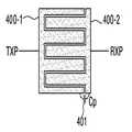
도3b는 실시예에 따른 압력 전극(400)의 구조를 예시한다. 압력 전극(400)은 예컨대 압력 구동전극(400-1)과 압력 수신전극(400-2)을 포함하여 구성될 수 있다. 다시 도3a에서, 거리(d)가 가까워짐에 따라 프린징(fringing) 현상에 의해 압력 구동전극(400-1)과 압력 수신전극(400-2) 사이에 생성되는 압력 캐패시터(401: Cp)의 정전용량 값이 감소할 수 있다. 압력 전극(400)이 기준 전위층(300)과 가까워질수록 압력 구동전극(400-1)과 압력 수신전극(400-2) 사이에 생성된 프린징 필드(fringing field)가 기준 전위층(300)으로 빼앗기는 구조이므로, 거리(d)가 감소함에 따라 압력 캐패시터(401)이 감소할 수 있다.3B illustrates the structure of the
실시예에 따른 압력 전극(400)은 터치 입력 장치(1000)내의 임의의 위치에 배치될 수 있다. 예컨대, 도3a에서 압력 전극(400)은 디스플레이 모듈(200) 하부에 배치될 수 있다. 이때, 기준 전위층(300)은 디스플레이 모듈(200)의 노이즈(noise) 차폐층일 수 있다. 또는, 기준 전위층(300)은 터치 입력 장치(1000)의 작동을 위한 메인보드(main board) 상의 중앙 처리 유닛(CPU) 또는 AP(Application Processor) 등으로부터 발생하는 노이즈 차폐를 위한 차폐층일 수 있다. 이때, 기준 전위층(300)은 터치 입력 장치(1000)에서 디스플레이 모듈(200)과 메인보드를 구분/지탱하기 위한 미드프레임(mid-frame)일 수 있다.The
도3a에서 압력 전극(400)이 디스플레이 모듈(200) 하부에 배치된 것이 예시되나 이는 단지 예시일뿐이며, 터치 입력 장치(1000) 내에서 기준 전위층(300)과 소정 거리 이격된 임의의 위치에 배치될 수 있다. 또한, 터치 입력 장치(1000)에서 디스플레이 모듈(200)의 상부면이 터치 표면을 구성하도록 예시되나, 이는 단지 예시일뿐이며 터치 표면은 임의의 다른 구성일 수 있으며 터치 표면에 대한 압력 인가에 따라 압력 전극(400)과 기준 전위층(300) 사이의 거리가 변화될 수 있으면 족하다.3A, the
또한, 도3a 및 도3b에서 압력 구동전극(400-1)과 압력 수신전극(400-2)이 동일한 층에 형성되고, 기준 전위층(300)과의 거리 변화에 따라 압력 구동전극(400-1)과 압력 수신전극(400-2) 사이의 정전용량 변화로부터 터치 압력을 검출하는 구조에 대해서 설명하였으나 이는 단지 예시일 뿐이며, 실시예에 따라 압력 구동전극(400-1)과 압력 수신전극(400-2)은 다른 원리 및 구조에 따라 터치 압력을 검출하도록 구성될 수 있다. 예컨대, 압력 구동전극(400-1)과 압력 수신전극(400-2)은 터치 입력 장치(1000)에서 서로 거리(d)로 이격되어, 터치 압력이 커짐에 따라 거리(d)가 감소하도록 배치될 수 있다. 따라서, 거리(d)가 감소하는 경우 압력 구동전극(400-1)과 압력 수신전극(400-2) 사이에 생성되는 정전용량 값이 감소할 수 있다.3A and 3B, the pressure-driving electrode 400-1 and the pressure-receiving electrode 400-2 are formed on the same layer, and the pressure-driving electrode 400- 1 and the pressure receiving electrode 400-2. However, the structure of the touch sensing electrode 400-1 and the pressure receiving electrode 400-2 is not limited thereto. 400-2 may be configured to detect the touch pressure according to different principles and structures. For example, the pressure driving electrode 400-1 and the pressure receiving electrode 400-2 are spaced apart from each other by a distance d in the
또한, 도3b에서 하나의 쌍의 압력 구동전극(400-1)과 압력 수신전극(400-2)이 압력전극으로서 예시되나, 압력전극은 복수의 쌍의 압력 구동전극과 압력 수신전극을 포함하여 구성될 수 있다. 이때, 압력 구동전극과 압력 수신전극의 쌍마다 하나의 채널을 구성할 수 있다. 따라서, 복수의 쌍의 압력 구동전극과 압력 수신전극을 포함하도록 압력전극을 구성함으로써 압력 검출을 위한 복수의 채널 구성이 가능하다. 이와 같이, 복수의 채널을 갖도록 압력전극을 구성함으로써 동시에 수행되는 복수의 터치에 대한 압력 검출이 가능하다.In FIG. 3B, one pair of the pressure driving electrode 400-1 and the pressure receiving electrode 400-2 are illustrated as pressure electrodes, but the pressure electrode includes a plurality of pairs of pressure driving electrodes and pressure receiving electrodes Lt; / RTI > At this time, one channel may be configured for each pair of the pressure-driven electrode and the pressure-receiving electrode. Therefore, a plurality of channel configurations for pressure detection are possible by configuring the pressure electrodes to include a plurality of pairs of pressure-driven electrodes and pressure-receiving electrodes. Thus, by configuring the pressure electrode to have a plurality of channels, it is possible to perform pressure detection for a plurality of touches performed at the same time.
또한, 도8 및 9를 참조하여 설명하는 바와 같이, 압력 전극(400)은 하나의 전극을 갖도록 구성될 수도 있다. 이때도 압력 검출을 위한 복수의 채널을 형성하도록 압력 전극(400)이 구성될 수 있음은 자명하다.Further, as described with reference to Figs. 8 and 9, the
이상에서 살펴본 바와 같이, 터치 압력을 검출하기 위해서 압력 전극(400)에서 발생하는 정전용량의 변화를 감지할 필요가 있다. 따라서, 압력 구동전극(400-1)에는 구동신호가 인가될 필요가 있고 압력 수신전극(400-2)으로부터 감지신호를 획득하여 정전용량의 변화량으로부터 터치 압력을 산출해야 한다. 이때, 터치 센서 패널(100)을 위한 구동부(110) 및 감지부(120)와 별개로 압력 검출을 위한 터치 센싱 IC가 제작된다면, 구동부(110), 감지부(120) 및 제어부(130)와 유사한 구성을 중복하여 포함하게 되므로 터치 입력 장치(1000)의 면적 및 부피가 커지는 문제점이 발생할 수 있다. 따라서, 본 발명의 실시예에서는 터치 센서 패널(100)을 위한 터치 검출기(150)를 거의 동일하게 이용하면서 이를 통해 압력 전극(400)으로부터 터치 압력 또한 검출하기 위한 기술을 제공하고자 한다.As described above, in order to detect the touch pressure, it is necessary to detect a change in the capacitance generated in the
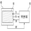
도4는 실시예에 따른 터치 검출기와 터치 센서 패널 및 압력 전극 사이의 신호 전달을 예시하는 개념도이다. 도4에 예시된 바와 같이, 실시예에 따른 터치 검출기(150)는 터치 센서 패널(100)로부터 터치 위치를 검출하면서 압력 전극(400)으로부터 터치 압력을 검출할 수 있도록 구성될 수 있다. 예컨대, 실시예에 따른 터치 검출기(150)는 터치 센서 패널(100)의 구동전극(TX)에 구동신호를 인가하고 수신전극(RX)으로부터 감지신호를 수신하여 터치 위치를 검출하도록 구성될 수 있다. 또한, 터치 검출기(150)는 압력 전극(400)에 구동신호를 인가하고 압력 전극(400)으로부터 감지신호를 수신하여 터치 압력의 크기를 검출하도록 구성될 수 있다. 즉, 실시예에서는 터치 센서 패널(100)로부터 터치 위치를 검출하고 압력 전극(400)으로부터 터치 압력의 크기를 모두 검출하도록 공통된 구성인 터치 검출기(150)가 이용될 수 있다.4 is a conceptual diagram illustrating signal transmission between a touch detector, a touch sensor panel, and a pressure electrode according to an embodiment. 4, the
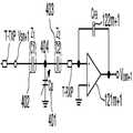
도5는 실시예에 따른 터치 검출 칩을 예시한다. 도5에 예시된 바와 같이, 실시예에 따른 터치 검출기(150)는 하나의 칩(one chip)으로 구성될 수 있다. 실시예에 따른 터치 검출기(150)는, 터치 검출기(150)에 포함된 구동부(110) 및 감지부(120)를 하나의 칩(chip) 상에 집적하여 구성되는 집적회로(IC: integrated Circuit)로 구현될 수 있다. 도5에 예시된 바와 같이, 터치 검출 칩(150C)은 복수의 입/출력 단자(T)를 구비할 수 있다. 이러한 입/출력 단자(T)는 핀(pin)으로 구현될 수 있다. 도5에서는 터치 검출 칩(150c)이 입/출력 단자(T)로서 n개의 구동신호 출력단자(T-TX1~T-TXn) 및 m개의 감지신호 입력단자(T-RX1~T-RXm), 그리고 1개의 압력 구동신호 출력단자(T-TXP) 및 1개의 압력 감지신호 입력단자(T-RXP)를 구비하는 것이 예시한다. 도5에서는 1개의 압력 구동신호 출력단자(T-TXP) 및 1개의 압력 감지신호 입력단자(T-RXP)를 포함하는 것이 예시되나, 예컨대, 압력 검출을 위한 복수의 채널을 형성하도록 압력전극(400)이 구성되는 경우, 터치 검출 칩(150c)이 복수의 압력 구동신호 출력단자(T-TXP) 및 복수의 압력 감지신호 입력단자(T-RXP)를 포함하도록 구성될 수 있다. 실시예에 따라, 터치 검출 칩(150C)은 다른 입출력 단자를 더 포함할 수 있으며, 도5에서는 전원전압 단자(T-VDD) 및 데이터 출력단자(T-DATA)를 더 포함하는 것이 예시된다.5 illustrates a touch detection chip according to an embodiment. As illustrated in FIG. 5, the
또한, 실시예에 따라 구동전극과 수신전극을 따로 구비하지 않고 하나의 전극을 통해 자기(self) 정전용량 검출 방식에 따라 터치 위치 및/또는 터치 압력을 검출하는 경우, 구동신호가 인가되는 출력단자와 감지신호가 수신되는 입력단자를 별개로 구성하지 않고 하나의 전극에 하나의 입/출력 단자를 통해 구동신호를 인가하고 감지신호를 수신하도록 구성될 수도 있다.According to the embodiment, when the touch position and / or the touch pressure is detected according to the self capacitance detection method through one electrode without separately providing the driving electrode and the receiving electrode, Output terminal and the input terminal through which the sensing signal is received, the driving signal may be applied to one electrode through one input / output terminal and the sensing signal may be received.
도5에서는 터치 검출 칩(150c)의 n개의 구동신호 출력단자(T-TX1~T-TXn)를 통해서 n개의 구동전극(TX1~TXn)에 구동신호가 각각 인가될 수 있으며 m개의 감지신호 입력단자(T-RX1~T-RXm)를 통해 m개의 수신전극(RX1~RXm)으로부터 감지신호가 각각 입력될 수 있다. 또한, 압력 구동신호 출력단자(T-TXP)를 통해 압력 구동신호가 압력 전극(400)에 인가될 수 있고 압력 감지신호 입력단자(T-RXP)를 통해 압력 감지신호가 압력 전극(400)으로부터 입력될 수 있다.5, a driving signal may be applied to n driving electrodes TX1 through TXn through n driving signal output terminals T-TX1 through T-TXn of the touch detection chip 150c, Sensing signals may be input from the m receiving electrodes RX1 to RXm through the terminals T-RX1 to T-RXm, respectively. A pressure drive signal may be applied to the
도6은 실시예에 따른 터치 입력 장치의 구동부, 감지부 및 전극부의 연결관계를 나타내는 등가 회로도를 예시한다. 도6을 참조하면, 실시예에 따른 터치 검출기(150)의 구동부(110)는 예컨대 복수의 구동회로(111 내지 11n 및 11n+1)을 포함하고 감지부(120)는 예컨대 복수의 감지회로(1201 내지 120m 및 120m+1)를 포함할 수 있다. 도6에서 "S"선 상단은 터치 센서 패널(100)에 대한 터치 위치를 검출하기 위한 구성이고 "S"선 하단은 압력 전극(400)으로부터 터치 압력의 크기를 검출하기 위한 구성이다.6 illustrates an equivalent circuit diagram illustrating a connection relationship between a driver, a sensing unit, and an electrode unit of the touch input device according to the embodiment. 6, the driving
제1 내지 제n구동회로(111 내지 11n)는 각각 복수의 구동전극 (TX1 내지 TXn)에 연결되어 구동신호를 전달할 수 있다. 이때, 구동회로(111 내지 11n)는 클록 생성기(clock generator) 및/또는 디지털/아날로그 버퍼(buffer)를 포함하여 구성될 수 있다.The first to n-th driving circuits 111 to 11n are connected to a plurality of driving electrodes TX1 to TXn, respectively, and can transmit a driving signal. At this time, the driving circuits 111 to 11n may include a clock generator and / or a digital / analog buffer.
제1 내지 제m감지회로(1201 내지 120m)는 노드 캐패시터(C1m 내지 Cnm)의 정전용량을 감지하여 터치 위치 정보를 획득할 수 있다. 도6에는, 설명의 편의를 위해 제m수신전극(RXm)을 통해 전달되는 노드 캐패시터(C11 내지 Cnm)의 정전용량을 감지하는 것만이 도시되므로, 터치 센서 패널(100)을 통해 터치 위치를 검출하기 위한 감지회로(1201 내지 120m) 중 제m감지회로(120m)만이 도시되어 있다. 제1노드 캐패시터(C11)는 일단이 제1구동전극(TX1)을 통해 제1구동회로(111)와 연결되고 타단은 제m수신전극(RXm)을 통해 제m감지부(120m)와 연결된다. 이와 마찬가지로 제2노드 캐피시터(C21) 내지 제n노드 캐피시터(Cnm)도 구동부(110)와 제m감지회로(120m)에 연결될 수 있다.The first to m-
또한, 제m감지회로(120m)는 증폭기(121m) 및 궤환 캐패시터(122m)를 포함하여 구성되는 캐패시턴스 센서를 포함하여 구성될 수 있다. 궤환 캐패시터(122m)는 증폭기(121m)의 반전단자(inverting terminal)와 증폭기(121m)의 출력단 사이, 즉 궤환 경로에 결합된 캐패시터이다. 이때, 증폭기(121m)의 비반전단자(non-inverting terminal)는 그라운드(Ground) 또는 기준 전위(Vref)에 접속될 수 있다. 또한, 캐패시턴스 센서는 궤환 캐패시터(122m)와 병렬로 연결되는 리셋 스위치(reset switch: 미도시)를 더 포함할 수 있다. 리셋 스위치는 캐패시턴스 센서에 의해 수행되는 전류에서 전압으로부터 변환을 리셋할 수 있다. 증폭기(121m)의 반전단자는 수신전극(RXm)을 통해 노드 캐패시터(C11 내지 Cnm) 의 정전용량에 대한 정보를 포함하는 전류 신호를 수신한 후 적분하여 전압 신호(Vom)로 변환할 수 있다. 증폭기(121m) 및 궤환 캐패시터(122m)를 포함하여 구성되는 캐패시턴스 센서를 통해 적분된 데이터는 ADC(123m)를 통해 디지털 데이터로 변환될 수 있다. 차후, 디지털 데이터는 프로세서 등에 입력되어 터치 센서 패널(100)에 대한 터치 위치 정보를 획득하도록 처리될 수 있다.In addition, the
실시예에 따른 터치 검출기(150) 및/또는 터치 검출 칩(150c)에서 구동부(110)에 포함된 복수의 구동회로 중 구동회로(예컨대, 제n+1 구동회로: 11n+1)는 압력 구동전극(400-1)에 구동신호(Vsn+1)를 인가하는데 이용될 수 있다. 또한, 감지부(120)에 포함된 복수의 감지회로 중 감지회로(예컨대, 제120m+1)는 압력 수신전극(400-1)으로부터, 압력 구동전극(400-1)과 압력 수신전극(400-2) 사이에 생성된 압력 캐패시터(401: Cp)의 정전용량을 감지하여 터치 압력의 크기를 검출할 수 있도록 구성될 수 있다. 도6에서는 하나의 구동회로(예컨대, 제n+1 구동회로: 11n+1) 및 하나의 감지회로(예컨대, 제120m+1)가 압력 검출을 위한 구동회로 및 감지회로로 예시되나, 실시예에 따라, 예컨대 압력 검출을 위한 복수의 채널이 형성되는 경우, 복수의 구동회로 및 복수의 감지회로가 압력 검출을 위한 구동회로 및 감지회로로 포함될 수 있다.The driving circuit (for example, the (n + 1) th driving circuit: 11n + 1) among the plurality of driving circuits included in the
도6에서 각각의 감지회로(1201 내지 120m+1)는 각각의 ADC(1231 내지 123m+1)를 포함하도록 예시되었으나, 감지부(120)는 하나의 공통된 ADC(123)를 포함하도록 구성될 수도 있다. 또한, 각각의 감지회로1201 내지 120m+1)에서 출력되는 데이터(DATA)는 도5에 예시된 하나의 데이터 출력단자(T-DATA)를 통해서 출력될 수 있다. 이때, 각각의 감지회로(1201 내지 120m+1)로부터의 데이터 신호는 서로 다른 헤더(header)를 갖도록 구성될 수 있다. 또한, 실시예에 따라 각각의 감지회로1201 내지 120m+1)에서 출력되는 데이터는 서로 다른 데이터 출력단자(T-DATA)를 통해서 출력되는 것도 가능하다.Although each of the
도6에서 알 수 있는 바와 같이, 실시예에 따른 터치 검출기(150)는 터치 압력을 검출하기 위해, 터치 위치를 검출하기 위한 구동회로(111 내지 11n)와 추가의 구동회로(11n+1)를 적어도 하나 더 포함하고, 터치 위치를 검출하기 위한 감지회로(120m)와 추가의 감지회로(120m+1)을 적어도 하나 더 포함할 수 있다. 이때, 압력 검출을 위한 구동회로(11n+1)는 구동회로(111 내지 11n)와 실질적으로 동일하게 구성될 수 있고 압력 검출을 위한 감지회로(120m+1)는 감지회로(120m)와 실질적으로 동일하게 구성될 수 있다. 실시예에 따른 터치 검출기(150) 및 터치 검출 칩(150C)은 터치 센서 패널(100)에 대한 터치 위치를 검출하기 위한 터치 검출기 및 터치 검출 칩에 대해 단순한 변형만을 가하여 터치 위치뿐 아니라 터치 압력 또한 검출하도록 구성될 수 있다.6, the
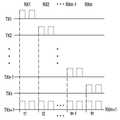
도7은 실시예에 따른 터치 검출기의 구동부에서 전극부에 인가되는 구동신호를 예시한다. 제어부(130)는 도7를 참조하여 설명하는 구동신호 인가 및 감지신호 수신이 수행되도록 구동부(110) 및 감지부(120)를 제어할 수 있다. 실시예에 따른 제어부(130)는 터치 검출 칩(150C)에 집적되도록 구현될 수 있다.7 illustrates a driving signal applied to the electrode unit in the driving unit of the touch detector according to the embodiment. The
예컨대, 구동부(120)는 터치 위치를 검출하기 위해 제1 내지 제n구동전극(TX1 내지 TXn)에 펄스 형태의 구동신호를 순차적으로 인가할 수 있다. 예컨대, 제1시간 구간(t1)에 구동신호가 제1구동전극(TX1)에 인가되고 제2시간 구간(t2)에 구동신호가 제2구동전극(TX2)에 인가되고, 이와 마찬가지로 제n시간 구간(tn)에 구동신호가 제n구동전극(TXn)에 인가될 수 있다. 이때, 터치 센서 패널(100)에 포함된 수신전극(RX1 내지 RXm)을 통해서 감지부(120)는 노드 캐패시터(C11 내지 Cnm)의 정전용량을 감지함으로써 터치 위치 및/또는 터치 여부를 검출할 수 있다.For example, the driving
이때, 구동부(110)는 제n+1시간 구간(tn+1; 미도시)에 구동신호를 압력 구동전극(400-1, 도7에서 TXn+1)에 인가하도록 구성되고 감지부(120)는 제n+1시간 구간에 압력 수신전극(400-2, 도7에서 RXm+1)으로부터 압력 캐패시터(401:Cp)의 정전용량을 감지함으로써 터치 압력을 검출하도록 동작할 수 있다. 이 경우, 터치 검출기(150, 150C)의 관점에서 압력 구동전극(400-1, 도7에서 TXn+1) 및 압력 수신전극(400-2, 도7에서 RXm+1)은 터치 센서 패널(100)에 포함된 구동전극(TX)과 수신전극(RX)과 동등하게 인식될 수 있다.At this time, the driving
터치 검출기(150, 150C)를 통한 터치 압력 검출시 노이즈(noise)를 최소화하고 터치 압력 크기의 검출 정밀도를 높이기 위해서, 예컨대 도7에 예시된 바와 같이 구동부(110)는 압력 구동전극(400-1, 도7에서 TXn+1)에 제1시간 구간(t1) 내지 제n시간 구간(tn+1) 동안에 구동신호를 지속적으로 인가하고, 이때 감지부(120)는 제1시간 구간(t1) 내지 제n시간 구간(tn+1) 동안에 압력 수신전극(400-2, 도7에서 RXm+1)을 통해 지속적으로 신호를 감지하여 감지된 신호를 이용하여 압력을 검출하는데 이용할 수 있다. 예컨대, 감지된 신호를 FIR(Finite Impulse Response: 유한 임펄스 응답) 필터링 처리하여 압력을 검출하는데 이용할 수 있다. 또는, 실시예에 따라 감지된 신호의 평균값을 이용하여 압력을 검출하는데 이용할 수 있다.In order to minimize noise during touch pressure detection through the
이 경우에, 터치 검출기(100)는 제1 내지 제n시간 구간 동안에 n개의 구동전극(TX1 내지 TXn) 및 m개의 수신전극(RX1 내지 RXm)을 포함하는 터치 센서 패널(100)로부터 터치 위치를 검출하기 위한 n * m개의 위치 검출 데이터 신호와, 1개의 압력 구동전극(TXn+1) 및 1개의 압력 수신전극(RXm+1)로부터 터치 압력을 검출하기 위한 1개의 압력 검출 데이터 신호를 출력할 수 있다. 즉, m개의 위치 검출용 수신전극(RX1 내지 RXm)가 각각 시간 구간마다 1개의 위치 데이터 신호를 출력할 수 있으므로, 1회 스캔시마다 n * m개의 위치 데이터 신호가 획득될 수 있으며 이때 1개의 압력 검출 데이터 신호가 출력될 수 있는 것이다.In this case, the
이상에서는 제1 내지 제n시간 구간 동안에 n개의 구동전극(TX1 내지 TXn)에 순차적으로 구동신호가 인가되는 경우에 대해서 설명하였으나, 실시예에 따라 n개의 구동전극(TX1 내지 TXn) 중 적어도 2개 이상의 구동전극에 동시에 구동신호가 인가되도록 동작할 수 있다.In the above description, the driving signals are sequentially applied to the n driving electrodes TX1 to TXn during the first to nth time periods. However, according to the embodiment, at least two of the n driving electrodes TX1 to TXn The driving signal can be simultaneously applied to the driving electrodes.
실시예에 따라, 압력 전극이 복수의 채널을 형성하도록 구성되는 경우, 1회 스캔시마다 복수개의 압력 검출 데이터 신호가 출력될 수 있음은 자명하다. 이때는, 복수의 압력 구동전극에 순차적으로 구동신호가 인가되도록 구성될 수 있다. 복수의 압력 구동전극에 대한 순차적 구동신호의 인가는, 제1 내지 제n구동전극(TX1 내지 TXn)에 대한 구동신호가 인가된 후 이루어지거나 제1 내지 제n구동전극(TX1 내지 TXn)에 대한 구동신호가 인가됨과 동시에 이루어질 수 있다. 또한, 실시예에 따라 적어도 2개 이상의 압력 구동전극에 동시에 구동신호가 인가되도록 동작할 수 있다.According to the embodiment, it is apparent that, when the pressure electrode is configured to form a plurality of channels, a plurality of pressure detection data signals can be output every one scan. In this case, the driving signal may be sequentially applied to the plurality of pressure driving electrodes. The application of the sequential driving signals to the plurality of pressure driving electrodes is performed after the driving signals for the first to the n-th driving electrodes TX1 to TXn are applied, or after the driving signals for the first to the n-th driving electrodes TX1 to TXn The driving signal can be applied simultaneously with the application of the driving signal. Also, according to the embodiment, the driving signal may be simultaneously applied to at least two or more pressure driving electrodes.
도8a 내지 도8c는 각각, 실시예에 따른 터치 입력 장치에서 제1대체예의 압력 전극 및 감지부의 등가 회로도, 압력 전극 구조, 및 압력 전극과 기준 전위층 사이의 거리 변화에 따른 감지부의 출력신호를 나타내는 그래프이다.8A to 8C are diagrams showing equivalent circuit diagrams of the pressure electrode and sensing unit of the first alternative example, the pressure electrode structure, and the output signal of the sensing unit according to the change in distance between the pressure electrode and the reference potential layer in the touch input apparatus according to the embodiment FIG.
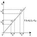
예컨대, 도8b에 예시된 바와 같이, 압력 전극(400)이 하나의 전극으로 구성되고, 도3에 도시된 바와 같이 기준 전위층(300)과 소정 거리(d) 이격되도록 터치 입력 장치(1000) 내에 배치된 경우를 예시한다. 이 경우, 도8b에 예시된 바와 같이, 압력 캐패시터(401)는 압력 전극(400)과 기준 전위층(300) 사이에 생성될 수 있으며, 거리(d)가 가까워질수록 압력 캐패시터(401)의 값은 커질 수 있다. 터치 검출기(150, 150C)는 이러한 압력 캐패시터(401) 값의 변화를 감지함으로써 터치 압력의 크기를 검출할 수 있다.For example, as illustrated in FIG. 8B, the
도8a에 예시된 바와 같이, 제1대체예에서 구동부(110)에서 구동신호(Vsn+1)를 압력 전극(400)에 인가하기 위한 구동신호 출력단자(T-TXP)와 압력 전극(400)으로부터 감지신호를 수신하기 위한 감지신호 입력단자(T-RXP) 사이에 압력 캐패시터(401)가 위치할 수 있다. 압력 캐패시터(401)는 결합부(404)와 기준 전위층(300)인 그라운드 사이에 위치하는 것으로 도시될 수 있다. 이때, 압력 캐패시터(401)는 압력 전극(400)과 기준 전위층(300) 사이의 거리에 따라 정전용량이 바뀌므로 가변하는 것으로 표시되었다.A driving signal output terminal T-TXP for applying the driving signal Vsn + 1 to the
제1대체예에서, 압력 캐패시터(401)를 통해 터치 압력을 검출하기 위해서는 압력 전극(400)은 제1임피던스(402)와 제2임피던스(403) 사이에 구성될 수 있다. 도8a에서는 제1임피던스(402)와 제2임피던스(403)가 모두 순수한 캐패시터(C1 및 C2)인 경우를 예시한다. 도8a과 같이 제1임피던스(402)와 제2임피던스(403)를 모두 캐패시터로 구성함으로써 터치 검출기(150)가 구동신호(Vs)의 동작 주파수에 의존하지 않는 성능을 제공할 수 있다.In a first alternative, the
도8a를 참조하면, 제1임피던스(402)와 제2임피던스(403)가 구동부(110)와 압력 전극(400) 사이 및 감지부(120)와 압력 전극(400) 사이로서 터치 검출기 및 터치 검출 칩(150, 150C)의 외부에 형성된 것으로 해석될 수 있다. 예컨대, 제1임피던스(402)와 제2임피던스(4033)는 칩 외부로서 칩과 전극을 연결하는 전도성 트레이스(trace) 등 상에 형성될 수 있다. 이때, 제1임피던스(402)와 제2임피던스(403)는 칩과 매우 근접하게 구성되어 있을 수 있다. 하지만, 이는 단지 구성상의 실시예일뿐이며, 제1임피던스(402)와 제2임피던스(403) 중 하나 또는 2개 모두 터치 검출기가 집적된 칩 상에 함께 집적되는 것도 가능하다. 제1임피던스(402)와 제2임피던스(403)가 칩내에 구현됨으로써 추가의 외부 소자에 대한 필요가 없어 단가를 낮출 수 있다. 제1임피던스(402)와 제2임피던스(403)가 모두 칩 내에 구현되는 경우, 압력 구동신호 출력단자(T-TXP) 및 압력 감지신호 입력단자(T-RXP)를 별개로 구성함이 없이 하나의 입출력단자를 통해 구동신호의 인가 및 감지신호의 수신이 가능할 수 있다. 또한, 임의의 압력 검출을 위한 전극에도 연결되어 균일한 압력 검출 성능을 제공할 수 있다.8A, a
제1대체예에서, 도3을 다시 참조하면, 객체(10)를 통해 압력이 인가되어 압력 전극(400)과 기준 전위층(300) 사이의 거리(d)가 감소하게 되면 압력 캐패시터(401)의 정전용량 값이 증가하게 된다. 도8a의 등가회로를 참조하여 캐패시턴스 센서의 출력 신호(Vo)와 구동 신호(Vs) 사이의 관계는 수학식(1)과 같이 표현될 수 있다.3, when pressure is applied through the object 10 and the distance d between the

수학식(1)을 참조하면, 출력신호(Vo)는 구동신호(Vs)의 주파수와는 무관한 결과를 얻을 수 있음을 알 수 있다. 이때, Cp>>C1+C2인 경우를 가정하면, 수학식(1)은 아래 수학식(2)와 같이 간소화될 수 있다.Referring to Equation (1), it can be seen that the output signal Vo is independent of the frequency of the driving signal Vs. At this time, assuming that Cp >> C1 + C2, the equation (1) can be simplified as shown in the following equation (2).

이때,
도8c는 실시예에 따른 압력 전극(400)과 기준 전위층(400) 사이의 거리변화에 따른 터치 검출기(150)의 출력 신호를 나타내는 그래프이다. 도8c의 그래프는 오프셋(offset) 등을 제거한 후의 그래프이다. 도8c를 참조하면, 압력 캐패시터(401)의 정전용량의 절대값에 편차가 발생하여도, 압력에 의한 거리(d)의 변화량이 동일하면 이에 따른 출력 신호(Vo)의 변화량도 일정하게 유지될 수 있음을 알 수 있다. 예컨대, 압력 전극(400)이 적용되는 제1애플리케이션(P-1)과 제2애플리케이션(P-2)에 따라 압력 전극(400)과 기준 전위층(300) 사이의 거리(d)는 서로 다를 수 있다. 하지만, 제1대체예에 따른 구성을 이용할 경우, 인가되는 압력에 따라 압력 전극(400)과 기준 전위층(300) 사이의 거리(d)의 변화량이 동일하다면(d1=d2) 출력 신호(Vo)의 변화량도 실질적으로 동일하게 유지(Vo1=Vo2)될 수 있는 것이다. 도8c에서 거리(d)와 출력 신호(Vo)가 서로 완전히 선형 관계를 갖는 것으로 도시되었으나 이는 단지 설명의 편의를 위한 것이며, 실시예에 따르면 실질적으로 선형 관계로 해석될 수 있을 정도로 거리(d)에 따라 출력 신호(Vo)가 변할 수 있다.8C is a graph showing an output signal of the
도9는 실시예에 따른 터치 입력 장치에서 제2대체예의 압력 전극 및 감지부의 등가 회로도이다.9 is an equivalent circuit diagram of the pressure electrode and sensing unit of the second alternative example in the touch input device according to the embodiment.
도9에서는 제1대체예에서, 제1임피던스(402)로 저항(R1)이 이용되는 경우에 구동신호(Vs)와 출력 신호(Vo) 사이의 등가회로를 도시한다. 제1임피던스로 저항(R1)이 이용되는 경우를 제외하고는 도8a과 동일하며 중복되는 설명은 생략한다.9 shows an equivalent circuit between the drive signal Vs and the output signal Vo when the resistor R1 is used as the
도9와 같은 제2대체예의 등가회로에서 구동신호(Vs)와 출력 신호(Vo) 사이의 전달함수는 아래 수학식(3)과 같이 표현될 수 있다.In the equivalent circuit of the second alternative example as shown in FIG. 9, the transfer function between the drive signal Vs and the output signal Vo can be expressed by the following equation (3).

여기서, Cp>>C2라고 가정하면, 수학식(3)은 수학식(4)와 같이 간소화될 수 있다.Here, assuming that Cp >

여기서, ω=2πf이며, f는 구동신호(Vs)의 주파수이다. 수학식(4)로부터 알 수 있는 바와 같이, 출력신호(Vo)의 크기는 구동신호(Vs)의 주파수가 커짐에 따라 점점 감소하게 된다.Here,? = 2? F and f is the frequency of the driving signal Vs. As can be seen from the equation (4), the magnitude of the output signal Vo gradually decreases as the frequency of the driving signal Vs increases.
이때, 비록 수학식(4)에 따르면 출력신호(Vo)와 거리(d) 사이에 완전한 선형 관계가 형성되지는 않지만 고정된 주파수에서 출력신호(Vo)와 거리(d) 사이에는 거의 선형적인 특성을 갖게 되므로 실시예에 따른 전체 시스템에서 제1대체예에서와 마찬가지로 신호 처리가 단순화될 수 있다. 이상에서는 제1임피던스(402)가 저항성 소자이고 제2임피던스(403)는 정전용량성 소자인 경우를 예로하여 설명하나, 제1임피던스(402)가 정전용량성 소자이고 제2임피던스(403)가 저항성 소자인 경우에도 적용될 수 있다.According to equation (4), although a complete linear relationship is not formed between the output signal Vo and the distance d, there is a substantially linear characteristic between the output signal Vo and the distance d at a fixed frequency, The signal processing can be simplified as in the first alternative example in the entire system according to the embodiment. Although the
도9를 참조하여 살펴본 바와 같이, 제1임피던스(402)와 제2임피던스(403) 중 적어도 어느 하나가 순수한 캐패시터 소자가 아니라 저항성 소자로 구성된 경우에는 구동신호(Vs)의 주파수에 따라 특성이 변화하는 출력신호를 획득하게 된다.9, when at least one of the
Cp 및 C2의 정전용량 값은 실시예/환경에 따라 변경될 수 있음은 자명하며, Cp로는 수백 pF(pico Farad) 범위 그리고 C2로는 수십 pF 범위의 정전용량 값을 적용하여 실험한 결과 출력신호(Vo)와 거리(d) 사이의 선형 관계 및 주파수에 따라 변하는 특성을 도출할 수 있었다.It is obvious that the capacitance values of Cp and C2 can be changed according to the embodiment / environment, and the capacitance value in the range of several hundreds pF (pico farad) and C2 several tens pF is applied to Cp, Vo) and the distance (d) and the characteristics varying according to the frequency.
또한, 이상에서 실시예를 중심으로 설명하였으나 이는 단지 예시일 뿐 본 발명을 한정하는 것이 아니며, 본 발명이 속하는 분야의 통상의 지식을 가진 자라면 본 실시예의 본질적인 특성을 벗어나지 않는 범위에서 이상에 예시되지 않은 여러 가지의 변형과 응용이 가능함을 알 수 있을 것이다. 예를 들어, 실시예에 구체적으로 나타난 각 구성 요소는 변형하여 실시할 수 있는 것이다. 그리고 이러한 변형과 응용에 관계된 차이점들은 첨부된 청구 범위에서 규정하는 본 발명의 범위에 포함되는 것으로 해석되어야 할 것이다.While the present invention has been particularly shown and described with reference to exemplary embodiments thereof, it is clearly understood that the same is by way of illustration and example only and is not to be taken by way of illustration, It can be seen that various modifications and applications are possible. For example, each component specifically shown in the embodiments can be modified and implemented. It is to be understood that all changes and modifications that come within the meaning and range of equivalency of the claims are therefore intended to be embraced therein.
1000: 터치 입력 장치 100: 터치 센서 패널
110: 구동부 120: 감지부
130: 제어부 200: 디스플레이 모듈
300: 기준 전위층 400: 압력 전극
150: 터치 검출기 150C: 터치 검출 칩
10: 객체1000: touch input device 100: touch sensor panel
110: driving unit 120:
130: control unit 200: display module
300: reference potential layer 400: pressure electrode
150:
10: Objects
Claims (34)
Translated fromKorean상기 복수의 전극 중 적어도 2개 이상의 전극으로부터 복수의 신호를 수신하여 터치 위치 및 터치 압력을 검출할 수 있도록 구성된 감지부; 및
상기 구동신호를 전달하기 위한 복수의 출력단자를 포함하며,
상기 복수의 출력단자 중 적어도 하나는 압력 검출만을 위한 압력 검출용 출력단자이고,
상기 구동신호가 인가되는 상기 적어도 2개 이상의 전극은 적어도 하나의 압력 검출용 구동전극과 n개의 위치 검출용 구동전극을 포함하고,
상기 구동부는, 제1시간구간에 상기 n개의 위치 검출용 구동전극에 구동신호를 인가하고 상기 제1시간구간과 다른 제2시간구간에 상기 적어도 하나의 압력 검출용 구동전극에 구동신호를 인가하도록 구성되며,
n은 자연수인,
터치 검출 칩.A driving unit configured to apply a driving signal to at least two or more of the plurality of electrodes;
A sensing unit configured to receive a plurality of signals from at least two or more of the plurality of electrodes and detect a touch position and a touch pressure; And
And a plurality of output terminals for transmitting the driving signal,
At least one of the plurality of output terminals is an output terminal for pressure detection for pressure detection only,
Wherein the at least two electrodes to which the driving signal is applied include at least one driving electrode for pressure detection and n driving electrodes for position detection,
Wherein the driving unit applies a driving signal to the n number of position detecting driving electrodes in a first time interval and applies a driving signal to the at least one driving electrode for pressure detection in a second time interval different from the first time interval Respectively,
n is a natural number,
Touch detection chip.
상기 구동신호가 인가되는 상기 적어도 2개 이상의 전극은 상기 복수의 신호를 수신하기 위한 상기 적어도 2개 이상의 전극과 동일하고,
상기 복수의 출력단자는, 상기 복수의 신호를 입력받기 위한 복수의 입력단자와 동일한,
터치 검출 칩.The method according to claim 1,
The at least two electrodes to which the driving signal is applied are the same as the at least two electrodes for receiving the plurality of signals,
Wherein the plurality of output terminals are the same as the plurality of input terminals for receiving the plurality of signals,
Touch detection chip.
상기 감지부는, 상기 제1시간구간에 상기 n개의 위치 검출용 구동전극으로부터 입력되는 신호를 통해 터치 위치를 검출하고 상기 제2시간구간에 상기 적어도 하나의 압력 검출용 구동전극으로부터 입력되는 신호를 통해 터치 압력을 검출하도록 구성된,
터치 검출 칩.3. The method of claim 2,
Wherein the sensing unit detects a touch position through a signal input from the n position detection driving electrodes in the first time interval and outputs the touch position in the second time interval through a signal input from the at least one pressure detection driving electrode Configured to detect touch pressure,
Touch detection chip.
상기 구동신호가 인가되는 상기 적어도 2개 이상의 전극은 상기 복수의 신호를 수신하기 위한 상기 적어도 2개 이상의 전극과 상이하고,
상기 복수의 신호를 입력받기 위한 복수의 입력단자를 더 포함하는,
터치 검출 칩.The method according to claim 1,
The at least two electrodes to which the driving signal is applied are different from the at least two electrodes for receiving the plurality of signals,
Further comprising a plurality of input terminals for receiving the plurality of signals,
Touch detection chip.
상기 구동부는, 상기 n개의 위치 검출용 구동전극 각각에 인가되는 구동신호와 동일한 구동신호를 상기 적어도 하나의 압력 검출용 구동전극 각각에 인가하도록 구성된,
터치 검출 칩.5. The method according to any one of claims 1 to 4,
Wherein the driving unit is configured to apply the same driving signal as the driving signal applied to each of the n position detecting driving electrodes to each of the at least one pressure detecting driving electrode,
Touch detection chip.
상기 구동부는, 상기 n개의 위치 검출용 구동전극 각각에 구동신호를 인가하도록 구성된 n개의 구동회로, 및 상기 적어도 하나의 압력 검출용 구동전극 각각에 구동신호를 인가하도록 구성되고 상기 구동회로와 동일하게 구성된 적어도 하나의 추가 구동회로를 포함하도록 구성된,
터치 검출 칩.5. The method according to any one of claims 1 to 4,
The driving unit may include n driving circuits configured to apply driving signals to the n position detecting driving electrodes and a driving circuit configured to apply a driving signal to each of the at least one pressure detecting driving electrode, And at least one additional drive circuit configured to drive the drive circuit,
Touch detection chip.
상기 감지부는, 각각 동일하게 구성된 적어도 2개 이상의 감지회로를 포함하도록 구성되며,
상기 적어도 2개 이상의 감지회로 중 적어도 하나는 압력 검출용 감지회로이고,
상기 적어도 2개 이상의 감지회로 중 상기 적어도 하나의 압력 검출용 감지회로를 제외한 나머지 감지회로는 위치 검출용 감지회로인,
터치 검출 칩.5. The method according to any one of claims 1 to 4,
The sensing unit is configured to include at least two sensing circuits each configured identically,
Wherein at least one of the at least two sensing circuits is a sensing circuit for sensing a pressure,
Wherein at least one of the at least two sensing circuits, except for the at least one pressure sensing sensing circuit, is a position sensing sensing circuit,
Touch detection chip.
상기 복수의 전극 중 적어도 2개 이상의 전극으로부터 복수의 신호를 수신하여 터치 위치 및 터치 압력을 검출할 수 있도록 구성된 감지부; 및
상기 구동신호를 전달하기 위한 복수의 출력단자를 포함하며,
상기 복수의 출력 단자 중 적어도 하나는 압력 검출만을 위한 압력 검출용 출력단자이고,
상기 구동신호가 인가되는 상기 적어도 2개 이상의 전극은 적어도 하나의 압력 검출용 구동전극과 n개의 위치 검출용 구동전극을 포함하고,
상기 구동부는, 상기 n개의 위치 검출용 구동전극에 구동신호를 인가하는 시간구간 동안에 상기 적어도 하나의 압력 검출용 구동전극에 구동신호를 인가하도록 구성되고,
n은 자연수인,
터치 검출 칩.A driving unit configured to apply a driving signal to at least two or more of the plurality of electrodes;
A sensing unit configured to receive a plurality of signals from at least two or more of the plurality of electrodes and detect a touch position and a touch pressure; And
And a plurality of output terminals for transmitting the driving signal,
At least one of the plurality of output terminals is an output terminal for pressure detection for pressure detection only,
Wherein the at least two electrodes to which the driving signal is applied include at least one driving electrode for pressure detection and n driving electrodes for position detection,
Wherein the driving unit is configured to apply a driving signal to the at least one driving electrode for pressure detection during a time period for applying a driving signal to the n position detecting driving electrodes,
n is a natural number,
Touch detection chip.
상기 구동신호가 인가되는 상기 적어도 2개 이상의 전극은 상기 복수의 신호를 수신하기 위한 상기 적어도 2개 이상의 전극과 동일하고,
상기 복수의 출력단자는, 상기 복수의 신호를 입력받기 위한 복수의 입력단자와 동일한,
터치 검출 칩.9. The method of claim 8,
The at least two electrodes to which the driving signal is applied are the same as the at least two electrodes for receiving the plurality of signals,
Wherein the plurality of output terminals are the same as the plurality of input terminals for receiving the plurality of signals,
Touch detection chip.
상기 구동부는, 상기 시간구간에 상기 n개의 위치 검출용 구동전극에 구동신호를 인가하고, 상기 시간구간에 상기 적어도 하나의 압력 검출용 구동전극 각각에 구동신호를 복수 회 인가하도록 구성되는,
터치 검출 칩.10. The method of claim 9,
Wherein the driving unit is configured to apply a driving signal to the n number of position detecting driving electrodes in the time interval and apply a driving signal to each of the at least one pressure detecting driving electrode plural times in the time interval,
Touch detection chip.
상기 감지부는, 상기 시간구간에 상기 적어도 하나의 압력 검출용 구동전극 각각으로부터 입력되는 복수개 신호의 평균을 이용하여 압력을 검출하도록 구성된,
터치 검출 칩.11. The method of claim 10,
Wherein the sensing unit is configured to detect a pressure using an average of a plurality of signals input from each of the at least one pressure detecting driving electrode in the time interval,
Touch detection chip.
상기 구동신호가 인가되는 상기 적어도 2개 이상의 전극은 상기 복수의 신호를 수신하기 위한 상기 적어도 2개 이상의 전극과 상이하고,
상기 복수의 신호를 입력받기 위한 복수의 입력단자를 더 포함하는,
터치 검출 칩.9. The method of claim 8,
The at least two electrodes to which the driving signal is applied are different from the at least two electrodes for receiving the plurality of signals,
Further comprising a plurality of input terminals for receiving the plurality of signals,
Touch detection chip.
상기 구동부는, 상기 시간구간에 상기 n개의 위치 검출용 구동전극에 구동신호를 인가하고, 상기 시간구간에 상기 적어도 하나의 압력 검출용 구동전극 각각에 구동신호를 복수 회 인가하도록 구성되는,
터치 검출 칩.13. The method of claim 12,
Wherein the driving unit is configured to apply a driving signal to the n number of position detecting driving electrodes in the time interval and apply a driving signal to each of the at least one pressure detecting driving electrode plural times in the time interval,
Touch detection chip.
상기 복수의 신호를 수신하기 위한 상기 적어도 2개 이상의 전극은 적어도 하나의 압력 검출용 수신전극을 포함하며,
상기 감지부는, 상기 시간구간에 상기 적어도 하나의 압력 검출용 수신전극 각각으로부터 입력되는 복수개 신호의 평균을 이용하여 압력을 검출하도록 구성된,
터치 검출 칩.14. The method of claim 13,
Wherein the at least two electrodes for receiving the plurality of signals comprise at least one pressure sensing receiving electrode,
Wherein the sensing unit is configured to detect a pressure using an average of a plurality of signals input from each of the at least one pressure sensing receiving electrode during the time interval,
Touch detection chip.
상기 구동부는, 상기 n개의 위치 검출용 구동전극 각각에 인가되는 구동신호와 동일한 구동신호를 상기 적어도 하나의 압력 검출용 구동전극 각각에 인가하도록 구성된,
터치 검출 칩.15. The method according to any one of claims 8 to 14,
Wherein the driving unit is configured to apply the same driving signal as the driving signal applied to each of the n position detecting driving electrodes to each of the at least one pressure detecting driving electrode,
Touch detection chip.
상기 구동부는, 상기 n개의 위치 검출용 구동전극 각각에 구동신호를 인가하도록 구성된 n개의 구동회로, 및 상기 적어도 하나의 압력 검출용 구동전극 각각에 구동신호를 인가하도록 구성되고 상기 구동회로와 동일하게 구성된 적어도 하나의 추가 구동회로를 포함하도록 구성된,
터치 검출 칩.15. The method according to any one of claims 8 to 14,
The driving unit may include n driving circuits configured to apply driving signals to the n position detecting driving electrodes and a driving circuit configured to apply a driving signal to each of the at least one pressure detecting driving electrode, And at least one additional drive circuit configured to drive the drive circuit,
Touch detection chip.
상기 감지부는, 각각 동일하게 구성된 적어도 2개 이상의 감지회로를 포함하도록 구성되며,
상기 적어도 2개 이상의 감지회로 중 적어도 하나는 압력 검출용 감지회로이고,
상기 적어도 2개 이상의 감지회로 중 상기 적어도 하나의 압력 검출용 감지회로를 제외한 나머지 감지회로는 위치 검출용 감지회로인,
터치 검출 칩.15. The method according to any one of claims 8 to 14,
The sensing unit is configured to include at least two sensing circuits each configured identically,
Wherein at least one of the at least two sensing circuits is a sensing circuit for sensing a pressure,
Wherein at least one of the at least two sensing circuits, except for the at least one pressure sensing sensing circuit, is a position sensing sensing circuit,
Touch detection chip.
터치 검출 칩을 포함하며,
상기 터치 검출 칩은:
복수의 전극 중 적어도 2개 이상의 전극에 구동신호를 인가할 수 있도록 구성된 구동부;
상기 복수의 전극 중 적어도 2개 이상의 전극으로부터 복수의 신호를 수신하여 터치 위치 및 터치 압력을 검출할 수 있도록 구성된 감지부; 및
상기 구동신호를 전달하기 위한 복수의 출력단자를 포함하며,
상기 복수의 출력단자 중 적어도 하나는 압력 검출만을 위한 압력 검출용 출력단자이고,
상기 구동신호가 인가되는 상기 적어도 2개 이상의 전극은 적어도 하나의 압력 검출용 구동전극과 n개의 위치 검출용 구동전극을 포함하고,
상기 구동부는, 제1시간구간에 상기 n개의 위치 검출용 구동전극에 구동신호를 인가하고 상기 제1시간구간과 다른 제2시간구간에 상기 적어도 하나의 압력 검출용 구동전극에 구동신호를 인가하도록 구성되고,
n은 자연수인,
터치 입력 장치.A plurality of electrodes; And
A touch detection chip,
The touch detection chip includes:
A driving unit configured to apply a driving signal to at least two or more of the plurality of electrodes;
A sensing unit configured to receive a plurality of signals from at least two or more of the plurality of electrodes and detect a touch position and a touch pressure; And
And a plurality of output terminals for transmitting the driving signal,
At least one of the plurality of output terminals is an output terminal for pressure detection for pressure detection only,
Wherein the at least two electrodes to which the driving signal is applied include at least one driving electrode for pressure detection and n driving electrodes for position detection,
Wherein the driving unit applies a driving signal to the n number of position detecting driving electrodes in a first time interval and applies a driving signal to the at least one driving electrode for pressure detection in a second time interval different from the first time interval Respectively,
n is a natural number,
Touch input device.
상기 구동신호가 인가되는 상기 적어도 2개 이상의 전극은 상기 복수의 신호를 수신하기 위한 상기 적어도 2개 이상의 전극과 동일하고,
상기 복수의 출력단자는, 상기 복수의 신호를 입력받기 위한 복수의 입력단자와 동일한,
터치 입력 장치.19. The method of claim 18,
The at least two electrodes to which the driving signal is applied are the same as the at least two electrodes for receiving the plurality of signals,
Wherein the plurality of output terminals are the same as the plurality of input terminals for receiving the plurality of signals,
Touch input device.
상기 감지부는, 상기 제1시간구간에 상기 n개의 위치 검출용 구동전극으로부터 입력되는 신호를 통해 터치 위치를 검출하고 상기 제2시간구간에 상기 적어도 하나의 압력 검출용 구동전극으로부터 입력되는 신호를 통해 터치 압력을 검출하도록 구성된,
터치 입력 장치.20. The method of claim 19,
Wherein the sensing unit detects a touch position through a signal input from the n position detection driving electrodes in the first time interval and outputs the touch position in the second time interval through a signal input from the at least one pressure detection driving electrode Configured to detect touch pressure,
Touch input device.
상기 구동신호가 인가되는 상기 적어도 2개 이상의 전극은 상기 복수의 신호를 수신하기 위한 상기 적어도 2개 이상의 전극과 상이하고,
상기 터치 검출 칩은 상기 복수의 신호를 입력받기 위한 복수의 입력단자를 더 포함하는,
터치 입력 장치.19. The method of claim 18,
The at least two electrodes to which the driving signal is applied are different from the at least two electrodes for receiving the plurality of signals,
Wherein the touch detection chip further comprises a plurality of input terminals for receiving the plurality of signals,
Touch input device.
상기 구동부는, 상기 n개의 위치 검출용 구동전극 각각에 인가되는 구동신호와 동일한 구동신호를 상기 적어도 하나의 압력 검출용 구동전극 각각에 인가하도록 구성된,
터치 입력 장치.22. The method according to any one of claims 18 to 21,
Wherein the driving unit is configured to apply the same driving signal as the driving signal applied to each of the n position detecting driving electrodes to each of the at least one pressure detecting driving electrode,
Touch input device.
상기 구동부는, 상기 n개의 위치 검출용 구동전극 각각에 구동신호를 인가하도록 구성된 n개의 구동회로, 및 상기 적어도 하나의 압력 검출용 구동전극 각각에 구동신호를 인가하도록 구성되고 상기 구동회로와 동일하게 구성된 적어도 하나의 추가 구동회로를 포함하도록 구성된,
터치 입력 장치.22. The method according to any one of claims 18 to 21,
The driving unit may include n driving circuits configured to apply driving signals to the n position detecting driving electrodes and a driving circuit configured to apply a driving signal to each of the at least one pressure detecting driving electrode, And at least one additional drive circuit configured to drive the drive circuit,
Touch input device.
상기 감지부는, 각각 동일하게 구성된 적어도 2개 이상의 감지회로를 포함하도록 구성되며,
상기 적어도 2개 이상의 감지회로 중 적어도 하나는 압력 검출용 감지회로이고,
상기 적어도 2개 이상의 감지회로 중 상기 적어도 하나의 압력 검출용 감지회로를 제외한 나머지 감지회로는 위치 검출용 감지회로인,
터치 입력 장치.22. The method according to any one of claims 18 to 21,
The sensing unit is configured to include at least two sensing circuits each configured identically,
Wherein at least one of the at least two sensing circuits is a sensing circuit for sensing a pressure,
Wherein at least one of the at least two sensing circuits, except for the at least one pressure sensing sensing circuit, is a position sensing sensing circuit,
Touch input device.
터치 검출 칩을 포함하며,
상기 터치 검출 칩은:
복수의 전극 중 적어도 2개 이상의 전극에 구동신호를 인가할 수 있도록 구성된 구동부;
상기 복수의 전극 중 적어도 2개 이상의 전극으로부터 복수의 신호를 수신하여 터치 위치 및 터치 압력을 검출할 수 있도록 구성된 감지부; 및
상기 구동신호를 전달하기 위한 복수의 출력단자를 포함하며,
상기 복수의 출력 단자 중 적어도 하나는 압력 검출만을 위한 압력 검출용 출력단자이고,
상기 구동신호가 인가되는 상기 적어도 2개 이상의 전극은 적어도 하나의 압력 검출용 구동전극과 n개의 위치 검출용 구동전극을 포함하고,
상기 구동부는, 상기 n개의 위치 검출용 구동전극에 구동신호를 인가하는 시간구간 동안에 상기 적어도 하나의 압력 검출용 구동전극에 구동신호를 인가하도록 구성되고,
n은 자연수인,
터치 입력 장치.A plurality of electrodes; And
A touch detection chip,
The touch detection chip includes:
A driving unit configured to apply a driving signal to at least two or more of the plurality of electrodes;
A sensing unit configured to receive a plurality of signals from at least two or more of the plurality of electrodes and detect a touch position and a touch pressure; And
And a plurality of output terminals for transmitting the driving signal,
At least one of the plurality of output terminals is an output terminal for pressure detection for pressure detection only,
Wherein the at least two electrodes to which the driving signal is applied include at least one driving electrode for pressure detection and n driving electrodes for position detection,
Wherein the driving unit is configured to apply a driving signal to the at least one driving electrode for pressure detection during a time period for applying a driving signal to the n position detecting driving electrodes,
n is a natural number,
Touch input device.
상기 구동신호가 인가되는 상기 적어도 2개 이상의 전극은 상기 복수의 신호를 수신하기 위한 상기 적어도 2개 이상의 전극과 동일하고,
상기 복수의 출력단자는, 상기 복수의 신호를 입력받기 위한 복수의 입력단자와 동일한,
터치 입력 장치.26. The method of claim 25,
The at least two electrodes to which the driving signal is applied are the same as the at least two electrodes for receiving the plurality of signals,
Wherein the plurality of output terminals are the same as the plurality of input terminals for receiving the plurality of signals,
Touch input device.
상기 구동부는, 상기 시간구간에 상기 n개의 위치 검출용 구동전극에 구동신호를 인가하고, 상기 시간구간에 상기 적어도 하나의 압력 검출용 구동전극 각각에 구동신호를 복수 회 인가하도록 구성되는,
터치 입력 장치.26. The method of claim 25,
Wherein the driving unit is configured to apply a driving signal to the n number of position detecting driving electrodes in the time interval and apply a driving signal to each of the at least one pressure detecting driving electrode plural times in the time interval,
Touch input device.
상기 감지부는, 상기 시간구간에 상기 적어도 하나의 압력 검출용 구동전극 각각으로부터 입력되는 복수개 신호의 평균을 이용하여 압력을 검출하도록 구성된,
터치 입력 장치.28. The method of claim 27,
Wherein the sensing unit is configured to detect a pressure using an average of a plurality of signals input from each of the at least one pressure detecting driving electrode in the time interval,
Touch input device.
상기 구동신호가 인가되는 상기 적어도 2개 이상의 전극은 상기 복수의 신호를 수신하기 위한 상기 적어도 2개 이상의 전극과 상이하고,
상기 터치 검출 칩은 상기 복수의 신호를 입력받기 위한 복수의 입력단자를 더 포함하는,
터치 입력 장치.26. The method of claim 25,
The at least two electrodes to which the driving signal is applied are different from the at least two electrodes for receiving the plurality of signals,
Wherein the touch detection chip further comprises a plurality of input terminals for receiving the plurality of signals,
Touch input device.
상기 구동부는, 상기 시간구간에 상기 n개의 위치 검출용 구동전극에 구동신호를 인가하고, 상기 시간구간에 상기 적어도 하나의 압력 검출용 구동전극 각각에 구동신호를 복수 회 인가하도록 구성되는,
터치 입력 장치.30. The method of claim 29,
Wherein the driving unit is configured to apply a driving signal to the n number of position detecting driving electrodes in the time interval and apply a driving signal to each of the at least one pressure detecting driving electrode plural times in the time interval,
Touch input device.
상기 복수의 신호를 수신하기 위한 상기 적어도 2개 이상의 전극은 적어도 하나의 압력 검출용 수신전극을 포함하며,
상기 감지부는, 상기 시간구간에 상기 적어도 하나의 압력 검출용 수신전극 각각으로부터 입력되는 복수개 신호의 평균을 이용하여 압력을 검출하도록 구성된,
터치 입력 장치.31. The method of claim 30,
Wherein the at least two electrodes for receiving the plurality of signals comprise at least one pressure sensing receiving electrode,
Wherein the sensing unit is configured to detect a pressure using an average of a plurality of signals input from each of the at least one pressure sensing receiving electrode during the time interval,
Touch input device.
상기 구동부는, 상기 n개의 위치 검출용 구동전극 각각에 인가되는 구동신호와 동일한 구동신호를 상기 적어도 하나의 압력 검출용 구동전극 각각에 인가하도록 구성된,
터치 입력 장치.32. The method according to any one of claims 25 to 31,
Wherein the driving unit is configured to apply the same driving signal as the driving signal applied to each of the n position detecting driving electrodes to each of the at least one pressure detecting driving electrode,
Touch input device.
상기 구동부는, 상기 n개의 위치 검출용 구동전극 각각에 구동신호를 인가하도록 구성된 n개의 구동회로, 및 상기 적어도 하나의 압력 검출용 구동전극 각각에 구동신호를 인가하도록 구성되고 상기 구동회로와 동일하게 구성된 적어도 하나의 추가 구동회로를 포함하도록 구성된,
터치 입력 장치.32. The method according to any one of claims 25 to 31,
The driving unit may include n driving circuits configured to apply driving signals to the n position detecting driving electrodes and a driving circuit configured to apply a driving signal to each of the at least one pressure detecting driving electrode, And at least one additional drive circuit configured to drive the drive circuit,
Touch input device.
상기 감지부는, 각각 동일하게 구성된 적어도 2개 이상의 감지회로를 포함하도록 구성되며,
상기 적어도 2개 이상의 감지회로 중 적어도 하나는 압력 검출용 감지회로이고,
상기 적어도 2개 이상의 감지회로 중 상기 적어도 하나의 압력 검출용 감지회로를 제외한 나머지 감지회로는 위치 검출용 감지회로인,
터치 입력 장치.32. The method according to any one of claims 25 to 31,
The sensing unit is configured to include at least two sensing circuits each configured identically,
Wherein at least one of the at least two sensing circuits is a sensing circuit for sensing a pressure,
Wherein at least one of the at least two sensing circuits, except for the at least one pressure sensing sensing circuit, is a position sensing sensing circuit,
Touch input device.
Priority Applications (1)
| Application Number | Priority Date | Filing Date | Title |
|---|---|---|---|
| KR1020170097543AKR101865305B1 (en) | 2017-08-01 | 2017-08-01 | Touch detection chip and touch input device |
Applications Claiming Priority (1)
| Application Number | Priority Date | Filing Date | Title |
|---|---|---|---|
| KR1020170097543AKR101865305B1 (en) | 2017-08-01 | 2017-08-01 | Touch detection chip and touch input device |
Related Parent Applications (1)
| Application Number | Title | Priority Date | Filing Date |
|---|---|---|---|
| KR1020150109385ADivisionKR101765650B1 (en) | 2015-08-03 | 2015-08-03 | Touch detector, touch detection chip and touch input device |
Publications (2)
| Publication Number | Publication Date |
|---|---|
| KR20170093768A KR20170093768A (en) | 2017-08-16 |
| KR101865305B1true KR101865305B1 (en) | 2018-06-07 |
Family
ID=59752485
Family Applications (1)
| Application Number | Title | Priority Date | Filing Date |
|---|---|---|---|
| KR1020170097543AActiveKR101865305B1 (en) | 2017-08-01 | 2017-08-01 | Touch detection chip and touch input device |
Country Status (1)
| Country | Link |
|---|---|
| KR (1) | KR101865305B1 (en) |
Citations (4)
| Publication number | Priority date | Publication date | Assignee | Title |
|---|---|---|---|---|
| KR20100038067A (en)* | 2008-10-02 | 2010-04-12 | 가부시키가이샤 와코무 | Combination touch and transducer input system and method |
| KR20100101773A (en)* | 2009-03-10 | 2010-09-20 | 엘지이노텍 주식회사 | Input device |
| WO2013089048A1 (en)* | 2011-12-16 | 2013-06-20 | 株式会社村田製作所 | Touch operation input device |
| KR20150031593A (en)* | 2013-09-16 | 2015-03-25 | 주식회사 하이딥 | Touch panel input apparatus and input detection method thereof |
- 2017
- 2017-08-01KRKR1020170097543Apatent/KR101865305B1/enactiveActive
Patent Citations (5)
| Publication number | Priority date | Publication date | Assignee | Title |
|---|---|---|---|---|
| KR20100038067A (en)* | 2008-10-02 | 2010-04-12 | 가부시키가이샤 와코무 | Combination touch and transducer input system and method |
| JP2014209361A (en)* | 2008-10-02 | 2014-11-06 | 株式会社ワコム | Input system and controller |
| KR20100101773A (en)* | 2009-03-10 | 2010-09-20 | 엘지이노텍 주식회사 | Input device |
| WO2013089048A1 (en)* | 2011-12-16 | 2013-06-20 | 株式会社村田製作所 | Touch operation input device |
| KR20150031593A (en)* | 2013-09-16 | 2015-03-25 | 주식회사 하이딥 | Touch panel input apparatus and input detection method thereof |
Also Published As
| Publication number | Publication date |
|---|---|
| KR20170093768A (en) | 2017-08-16 |
Similar Documents
| Publication | Publication Date | Title |
|---|---|---|
| KR101765650B1 (en) | Touch detector, touch detection chip and touch input device | |
| JP7198469B2 (en) | smartphone | |
| US10331267B2 (en) | Touch detection method and touch detector performing the same | |
| KR102330372B1 (en) | Touch input device | |
| KR101739791B1 (en) | Pressure sensor, pressure detector and touch input device including the same | |
| KR101670447B1 (en) | Smartphone | |
| KR101506511B1 (en) | Capacitive location and pressure touch sensing device | |
| JP2017016675A (en) | Electrode sheet and touch input device | |
| KR101633923B1 (en) | Smartphone | |
| KR101965871B1 (en) | Force-touch panel, and fource-touch detection device and display system having the same | |
| KR20160016733A (en) | Touch input device | |
| KR101865305B1 (en) | Touch detection chip and touch input device | |
| KR101960708B1 (en) | Touch input device | |
| KR20160141881A (en) | Touch input device | |
| KR101872209B1 (en) | Touch input device | |
| KR102124625B1 (en) | Touch input device | |
| KR20190038770A (en) | Force-touch panel, and fource-touch detection device and display system having the same | |
| KR20160016726A (en) | Electrode sheet and touch input device |
Legal Events
| Date | Code | Title | Description |
|---|---|---|---|
| A107 | Divisional application of patent | ||
| A201 | Request for examination | ||
| PA0107 | Divisional application | Comment text:Divisional Application of Patent Patent event date:20170801 Patent event code:PA01071R01D Filing date:20150803 Application number text:1020150109385 | |
| PA0201 | Request for examination | ||
| PG1501 | Laying open of application | ||
| E902 | Notification of reason for refusal | ||
| PE0902 | Notice of grounds for rejection | Comment text:Notification of reason for refusal Patent event date:20170822 Patent event code:PE09021S01D | |
| E701 | Decision to grant or registration of patent right | ||
| PE0701 | Decision of registration | Patent event code:PE07011S01D Comment text:Decision to Grant Registration Patent event date:20180328 | |
| PR0701 | Registration of establishment | Comment text:Registration of Establishment Patent event date:20180531 Patent event code:PR07011E01D | |
| PR1002 | Payment of registration fee | Payment date:20180601 End annual number:3 Start annual number:1 | |
| PG1601 | Publication of registration | ||
| PR1001 | Payment of annual fee | Payment date:20210503 Start annual number:4 End annual number:4 | |
| PR1001 | Payment of annual fee | Payment date:20220504 Start annual number:5 End annual number:5 | |
| PR1001 | Payment of annual fee | Payment date:20240502 Start annual number:7 End annual number:7 |