KR101857335B1 - Method and device for providing through-openings in a substrate and a substrate produced in said manner - Google Patents
Method and device for providing through-openings in a substrate and a substrate produced in said mannerDownload PDFInfo
- Publication number
- KR101857335B1 KR101857335B1KR1020157027412AKR20157027412AKR101857335B1KR 101857335 B1KR101857335 B1KR 101857335B1KR 1020157027412 AKR1020157027412 AKR 1020157027412AKR 20157027412 AKR20157027412 AKR 20157027412AKR 101857335 B1KR101857335 B1KR 101857335B1
- Authority
- KR
- South Korea
- Prior art keywords
- substrate
- laser beam
- laser
- optical system
- recesses
- Prior art date
- Legal status (The legal status is an assumption and is not a legal conclusion. Google has not performed a legal analysis and makes no representation as to the accuracy of the status listed.)
- Active
Links
- 239000000758substrateSubstances0.000titleclaimsabstractdescription122
- 238000000034methodMethods0.000titleclaimsabstractdescription75
- 239000000463materialSubstances0.000claimsabstractdescription36
- 230000004048modificationEffects0.000claimsabstractdescription28
- 238000012986modificationMethods0.000claimsabstractdescription28
- 230000003287optical effectEffects0.000claimsabstractdescription27
- 230000001419dependent effectEffects0.000claimsabstractdescription16
- 238000005530etchingMethods0.000claimsdescription29
- 238000003754machiningMethods0.000claimsdescription22
- 229910052751metalInorganic materials0.000claimsdescription14
- 239000002184metalSubstances0.000claimsdescription14
- 239000011521glassSubstances0.000claimsdescription11
- 239000010980sapphireSubstances0.000claimsdescription7
- 229910052594sapphireInorganic materials0.000claimsdescription7
- 239000010703siliconSubstances0.000claimsdescription7
- 229910052710siliconInorganic materials0.000claimsdescription7
- KRHYYFGTRYWZRS-UHFFFAOYSA-NFluoraneChemical compoundFKRHYYFGTRYWZRS-UHFFFAOYSA-N0.000claimsdescription4
- 230000007423decreaseEffects0.000claimsdescription3
- 230000002123temporal effectEffects0.000claimsdescription3
- 239000011248coating agentSubstances0.000claims1
- 238000000576coating methodMethods0.000claims1
- 230000009471actionEffects0.000abstractdescription10
- 230000008859changeEffects0.000abstractdescription6
- 230000003247decreasing effectEffects0.000abstractdescription3
- 239000011799hole materialSubstances0.000description12
- 230000008569processEffects0.000description12
- 230000000694effectsEffects0.000description8
- XUIMIQQOPSSXEZ-UHFFFAOYSA-NSiliconChemical compound[Si]XUIMIQQOPSSXEZ-UHFFFAOYSA-N0.000description6
- 230000035515penetrationEffects0.000description5
- 239000004020conductorSubstances0.000description4
- 239000007789gasSubstances0.000description4
- 239000003365glass fiberSubstances0.000description4
- 238000004519manufacturing processMethods0.000description4
- KWYUFKZDYYNOTN-UHFFFAOYSA-MPotassium hydroxideChemical compound[OH-].[K+]KWYUFKZDYYNOTN-UHFFFAOYSA-M0.000description3
- 238000009826distributionMethods0.000description3
- 239000007788liquidSubstances0.000description3
- 230000000149penetrating effectEffects0.000description3
- 239000004065semiconductorSubstances0.000description3
- 239000012780transparent materialSubstances0.000description3
- 229910000323aluminium silicateInorganic materials0.000description2
- 230000008901benefitEffects0.000description2
- 238000010586diagramMethods0.000description2
- 238000005516engineering processMethods0.000description2
- 239000003822epoxy resinSubstances0.000description2
- 229920000647polyepoxidePolymers0.000description2
- 239000000243solutionSubstances0.000description2
- 238000009834vaporizationMethods0.000description2
- 230000008016vaporizationEffects0.000description2
- RYGMFSIKBFXOCR-UHFFFAOYSA-NCopperChemical compound[Cu]RYGMFSIKBFXOCR-UHFFFAOYSA-N0.000description1
- VYPSYNLAJGMNEJ-UHFFFAOYSA-NSilicium dioxideChemical compoundO=[Si]=OVYPSYNLAJGMNEJ-UHFFFAOYSA-N0.000description1
- 239000007864aqueous solutionSubstances0.000description1
- 230000015556catabolic processEffects0.000description1
- 239000000919ceramicSubstances0.000description1
- 239000003795chemical substances by applicationSubstances0.000description1
- 229910052802copperInorganic materials0.000description1
- 239000010949copperSubstances0.000description1
- 239000013078crystalSubstances0.000description1
- HNPSIPDUKPIQMN-UHFFFAOYSA-Ndioxosilane;oxo(oxoalumanyloxy)alumaneChemical compoundO=[Si]=O.O=[Al]O[Al]=OHNPSIPDUKPIQMN-UHFFFAOYSA-N0.000description1
- 238000001312dry etchingMethods0.000description1
- 238000010438heat treatmentMethods0.000description1
- 239000012212insulatorSubstances0.000description1
- 239000000203mixtureSubstances0.000description1
- 239000004033plasticSubstances0.000description1
- 239000011148porous materialSubstances0.000description1
- 230000009467reductionEffects0.000description1
- 238000002407reformingMethods0.000description1
- 239000005368silicate glassSubstances0.000description1
- 239000000126substanceSubstances0.000description1
- 239000012808vapor phaseSubstances0.000description1
Images


Classifications
- B23K26/0057—
- B—PERFORMING OPERATIONS; TRANSPORTING
- B23—MACHINE TOOLS; METAL-WORKING NOT OTHERWISE PROVIDED FOR
- B23K—SOLDERING OR UNSOLDERING; WELDING; CLADDING OR PLATING BY SOLDERING OR WELDING; CUTTING BY APPLYING HEAT LOCALLY, e.g. FLAME CUTTING; WORKING BY LASER BEAM
- B23K26/00—Working by laser beam, e.g. welding, cutting or boring
- B23K26/18—Working by laser beam, e.g. welding, cutting or boring using absorbing layers on the workpiece, e.g. for marking or protecting purposes
- B—PERFORMING OPERATIONS; TRANSPORTING
- B23—MACHINE TOOLS; METAL-WORKING NOT OTHERWISE PROVIDED FOR
- B23K—SOLDERING OR UNSOLDERING; WELDING; CLADDING OR PLATING BY SOLDERING OR WELDING; CUTTING BY APPLYING HEAT LOCALLY, e.g. FLAME CUTTING; WORKING BY LASER BEAM
- B23K26/00—Working by laser beam, e.g. welding, cutting or boring
- B23K26/36—Removing material
- B23K26/38—Removing material by boring or cutting
- B23K26/382—Removing material by boring or cutting by boring
- B—PERFORMING OPERATIONS; TRANSPORTING
- B23—MACHINE TOOLS; METAL-WORKING NOT OTHERWISE PROVIDED FOR
- B23K—SOLDERING OR UNSOLDERING; WELDING; CLADDING OR PLATING BY SOLDERING OR WELDING; CUTTING BY APPLYING HEAT LOCALLY, e.g. FLAME CUTTING; WORKING BY LASER BEAM
- B23K26/00—Working by laser beam, e.g. welding, cutting or boring
- B23K26/0006—Working by laser beam, e.g. welding, cutting or boring taking account of the properties of the material involved
- B—PERFORMING OPERATIONS; TRANSPORTING
- B23—MACHINE TOOLS; METAL-WORKING NOT OTHERWISE PROVIDED FOR
- B23K—SOLDERING OR UNSOLDERING; WELDING; CLADDING OR PLATING BY SOLDERING OR WELDING; CUTTING BY APPLYING HEAT LOCALLY, e.g. FLAME CUTTING; WORKING BY LASER BEAM
- B23K26/00—Working by laser beam, e.g. welding, cutting or boring
- B23K26/02—Positioning or observing the workpiece, e.g. with respect to the point of impact; Aligning, aiming or focusing the laser beam
- B23K26/06—Shaping the laser beam, e.g. by masks or multi-focusing
- B23K26/062—Shaping the laser beam, e.g. by masks or multi-focusing by direct control of the laser beam
- B23K26/0622—Shaping the laser beam, e.g. by masks or multi-focusing by direct control of the laser beam by shaping pulses
- B23K26/0624—Shaping the laser beam, e.g. by masks or multi-focusing by direct control of the laser beam by shaping pulses using ultrashort pulses, i.e. pulses of 1ns or less
- B—PERFORMING OPERATIONS; TRANSPORTING
- B23—MACHINE TOOLS; METAL-WORKING NOT OTHERWISE PROVIDED FOR
- B23K—SOLDERING OR UNSOLDERING; WELDING; CLADDING OR PLATING BY SOLDERING OR WELDING; CUTTING BY APPLYING HEAT LOCALLY, e.g. FLAME CUTTING; WORKING BY LASER BEAM
- B23K26/00—Working by laser beam, e.g. welding, cutting or boring
- B23K26/02—Positioning or observing the workpiece, e.g. with respect to the point of impact; Aligning, aiming or focusing the laser beam
- B23K26/06—Shaping the laser beam, e.g. by masks or multi-focusing
- B23K26/064—Shaping the laser beam, e.g. by masks or multi-focusing by means of optical elements, e.g. lenses, mirrors or prisms
- B—PERFORMING OPERATIONS; TRANSPORTING
- B23—MACHINE TOOLS; METAL-WORKING NOT OTHERWISE PROVIDED FOR
- B23K—SOLDERING OR UNSOLDERING; WELDING; CLADDING OR PLATING BY SOLDERING OR WELDING; CUTTING BY APPLYING HEAT LOCALLY, e.g. FLAME CUTTING; WORKING BY LASER BEAM
- B23K26/00—Working by laser beam, e.g. welding, cutting or boring
- B23K26/36—Removing material
- B23K26/40—Removing material taking account of the properties of the material involved
- B23K26/402—Removing material taking account of the properties of the material involved involving non-metallic material, e.g. isolators
- B—PERFORMING OPERATIONS; TRANSPORTING
- B23—MACHINE TOOLS; METAL-WORKING NOT OTHERWISE PROVIDED FOR
- B23K—SOLDERING OR UNSOLDERING; WELDING; CLADDING OR PLATING BY SOLDERING OR WELDING; CUTTING BY APPLYING HEAT LOCALLY, e.g. FLAME CUTTING; WORKING BY LASER BEAM
- B23K26/00—Working by laser beam, e.g. welding, cutting or boring
- B23K26/50—Working by transmitting the laser beam through or within the workpiece
- B23K26/53—Working by transmitting the laser beam through or within the workpiece for modifying or reforming the material inside the workpiece, e.g. for producing break initiation cracks
- H—ELECTRICITY
- H01—ELECTRIC ELEMENTS
- H01L—SEMICONDUCTOR DEVICES NOT COVERED BY CLASS H10
- H01L21/00—Processes or apparatus adapted for the manufacture or treatment of semiconductor or solid state devices or of parts thereof
- H01L21/02—Manufacture or treatment of semiconductor devices or of parts thereof
- H01L21/04—Manufacture or treatment of semiconductor devices or of parts thereof the devices having potential barriers, e.g. a PN junction, depletion layer or carrier concentration layer
- H01L21/18—Manufacture or treatment of semiconductor devices or of parts thereof the devices having potential barriers, e.g. a PN junction, depletion layer or carrier concentration layer the devices having semiconductor bodies comprising elements of Group IV of the Periodic Table or AIIIBV compounds with or without impurities, e.g. doping materials
- H01L21/30—Treatment of semiconductor bodies using processes or apparatus not provided for in groups H01L21/20 - H01L21/26
- H—ELECTRICITY
- H01—ELECTRIC ELEMENTS
- H01L—SEMICONDUCTOR DEVICES NOT COVERED BY CLASS H10
- H01L21/00—Processes or apparatus adapted for the manufacture or treatment of semiconductor or solid state devices or of parts thereof
- H01L21/02—Manufacture or treatment of semiconductor devices or of parts thereof
- H01L21/04—Manufacture or treatment of semiconductor devices or of parts thereof the devices having potential barriers, e.g. a PN junction, depletion layer or carrier concentration layer
- H01L21/48—Manufacture or treatment of parts, e.g. containers, prior to assembly of the devices, using processes not provided for in a single one of the groups H01L21/18 - H01L21/326 or H10D48/04 - H10D48/07
- H01L21/4814—Conductive parts
- H01L21/4846—Leads on or in insulating or insulated substrates, e.g. metallisation
- H01L21/486—Via connections through the substrate with or without pins
- H—ELECTRICITY
- H01—ELECTRIC ELEMENTS
- H01S—DEVICES USING THE PROCESS OF LIGHT AMPLIFICATION BY STIMULATED EMISSION OF RADIATION [LASER] TO AMPLIFY OR GENERATE LIGHT; DEVICES USING STIMULATED EMISSION OF ELECTROMAGNETIC RADIATION IN WAVE RANGES OTHER THAN OPTICAL
- H01S3/00—Lasers, i.e. devices using stimulated emission of electromagnetic radiation in the infrared, visible or ultraviolet wave range
- H01S3/005—Optical devices external to the laser cavity, specially adapted for lasers, e.g. for homogenisation of the beam or for manipulating laser pulses, e.g. pulse shaping
- H01S3/0057—Temporal shaping, e.g. pulse compression, frequency chirping
- B—PERFORMING OPERATIONS; TRANSPORTING
- B23—MACHINE TOOLS; METAL-WORKING NOT OTHERWISE PROVIDED FOR
- B23K—SOLDERING OR UNSOLDERING; WELDING; CLADDING OR PLATING BY SOLDERING OR WELDING; CUTTING BY APPLYING HEAT LOCALLY, e.g. FLAME CUTTING; WORKING BY LASER BEAM
- B23K2101/00—Articles made by soldering, welding or cutting
- B23K2101/36—Electric or electronic devices
- B23K2101/40—Semiconductor devices
- B—PERFORMING OPERATIONS; TRANSPORTING
- B23—MACHINE TOOLS; METAL-WORKING NOT OTHERWISE PROVIDED FOR
- B23K—SOLDERING OR UNSOLDERING; WELDING; CLADDING OR PLATING BY SOLDERING OR WELDING; CUTTING BY APPLYING HEAT LOCALLY, e.g. FLAME CUTTING; WORKING BY LASER BEAM
- B23K2103/00—Materials to be soldered, welded or cut
- B23K2103/50—Inorganic material, e.g. metals, not provided for in B23K2103/02 – B23K2103/26
- B23K2103/54—Glass
- B—PERFORMING OPERATIONS; TRANSPORTING
- B23—MACHINE TOOLS; METAL-WORKING NOT OTHERWISE PROVIDED FOR
- B23K—SOLDERING OR UNSOLDERING; WELDING; CLADDING OR PLATING BY SOLDERING OR WELDING; CUTTING BY APPLYING HEAT LOCALLY, e.g. FLAME CUTTING; WORKING BY LASER BEAM
- B23K2103/00—Materials to be soldered, welded or cut
- B23K2103/50—Inorganic material, e.g. metals, not provided for in B23K2103/02 – B23K2103/26
- B23K2103/56—Inorganic material, e.g. metals, not provided for in B23K2103/02 – B23K2103/26 semiconducting
- B23K2201/40—
- B23K2203/50—
- B23K2203/56—
- H—ELECTRICITY
- H01—ELECTRIC ELEMENTS
- H01L—SEMICONDUCTOR DEVICES NOT COVERED BY CLASS H10
- H01L23/00—Details of semiconductor or other solid state devices
- H01L23/12—Mountings, e.g. non-detachable insulating substrates
- H01L23/14—Mountings, e.g. non-detachable insulating substrates characterised by the material or its electrical properties
- H01L23/147—Semiconductor insulating substrates
- H—ELECTRICITY
- H01—ELECTRIC ELEMENTS
- H01L—SEMICONDUCTOR DEVICES NOT COVERED BY CLASS H10
- H01L23/00—Details of semiconductor or other solid state devices
- H01L23/12—Mountings, e.g. non-detachable insulating substrates
- H01L23/14—Mountings, e.g. non-detachable insulating substrates characterised by the material or its electrical properties
- H01L23/15—Ceramic or glass substrates
- H—ELECTRICITY
- H01—ELECTRIC ELEMENTS
- H01L—SEMICONDUCTOR DEVICES NOT COVERED BY CLASS H10
- H01L23/00—Details of semiconductor or other solid state devices
- H01L23/48—Arrangements for conducting electric current to or from the solid state body in operation, e.g. leads, terminal arrangements ; Selection of materials therefor
- H01L23/488—Arrangements for conducting electric current to or from the solid state body in operation, e.g. leads, terminal arrangements ; Selection of materials therefor consisting of soldered or bonded constructions
- H01L23/498—Leads, i.e. metallisations or lead-frames on insulating substrates, e.g. chip carriers
- H01L23/49827—Via connections through the substrates, e.g. pins going through the substrate, coaxial cables
Landscapes
- Engineering & Computer Science (AREA)
- Physics & Mathematics (AREA)
- Optics & Photonics (AREA)
- Plasma & Fusion (AREA)
- Mechanical Engineering (AREA)
- Chemical & Material Sciences (AREA)
- Chemical Kinetics & Catalysis (AREA)
- Oil, Petroleum & Natural Gas (AREA)
- General Chemical & Material Sciences (AREA)
- Computer Hardware Design (AREA)
- Microelectronics & Electronic Packaging (AREA)
- Power Engineering (AREA)
- Condensed Matter Physics & Semiconductors (AREA)
- Manufacturing & Machinery (AREA)
- General Physics & Mathematics (AREA)
- Ceramic Engineering (AREA)
- Laser Beam Processing (AREA)
- Electromagnetism (AREA)
- Surface Treatment Of Glass (AREA)
Abstract
Translated fromKoreanDescription
Translated fromKorean본 발명은 레이저 광선을 이용해, 인터포저 (interposer) 또는 마이크로 부품으로서 이용될 수 있는 기판 안으로 다수의 관통 개구부를 도입하기 위한 방법 및 장치에 관한 것이다. 또한, 본 발명은 이러한 방식으로 제조된, 관통 개구부들이 제공된 기판에 관한 것이다.The present invention relates to a method and apparatus for introducing a plurality of through openings into a substrate, which can be used as an interposer or a micro-part, using a laser beam. The present invention also relates to a substrate provided with through openings, manufactured in this manner.
이러한 유형의 기판들은 다수의 동종 또는 이종 마이크로칩들의 연결부들을 전기적으로 연결하기 위한 이른바 인터포저로서 이용된다. 인터포저는 일반적으로 유리 또는 규소로 구성되고, 예컨대 접촉면들, 재배선, 관통 접촉부, 및 능동적 및 비능동적 구성요소들을 포함한다.This type of substrate is used as a so-called interposer for electrically connecting the connections of many homogeneous or heterogeneous microchips. The interposer is generally constructed of glass or silicon and includes, for example, contact surfaces, rewiring, penetrating contacts, and active and non-active components.
프로세서 코어로서의 마이크로칩은 전형적으로 그의 밑면에 비교적 작은 표면에 분배되어 서로 좁은 간격을 둔 수백개의 접촉점을 갖는다. 이 좁은 간격 때문에 이 접촉점들은 바로 회로판, 이른바 마더보드 위에 도포될 수 없다. 그렇기 때문에 인터포저가 연결요소로서 이용되고, 상기 연결요소를 가지고 접촉 베이스가 확장될 수 있다.A microchip as a processor core typically has hundreds of contact points spaced at a small distance from one another on a relatively small surface on its underside. Because of this narrow gap, these contact points can not be directly applied to the circuit board, so-called motherboard. Therefore, the interposer is used as a connecting element, and the contact base can be extended with the connecting element.
인터포저로서는, 실무에서 예컨대 유리섬유로 강화된 에폭시 수지 플레이트가 이용되고, 상기 에폭시 수지 플레이트에 다수의 구멍이 제공된다. 유리섬유 매트의 표면에 도체 트랙들 (conductor tracks) 이 연장되고, 구멍들을 채우기 위해 상기 도체 트랙들은 각각의 구멍들 안으로 안내되고, 상기 유리섬유 매트의 다른 측에서는 프로세서 코어의 연결 접촉부들까지 이어진다. 하지만, 가열 발생시 프로세서 코어와 유리섬유 매트 사이의 서로 다른 팽창들이 발생하고, 이로써 이 두 구성요소 사이의 기계적 응력들이 발생한다As an interposer, for example, an epoxy resin plate reinforced with glass fiber is used in the practice, and the epoxy resin plate is provided with a plurality of holes. Conductor tracks are extended to the surface of the glass fiber mat and the conductor tracks are guided into respective holes to fill the holes and to the connection contacts of the processor core on the other side of the glass fiber mat. However, when heat is generated, different expansions occur between the processor core and the glass fiber mat, resulting in mechanical stresses between the two components
그러므로, 서로 다른 열팽창계수들 때문에 발생하는 응력들을 감소시키기 위해 규소 인터포저들도 이용된다. 규소 인터포저들은 반도체 분야에서 통례적인 방식으로 가공될 수 있다. 하지만, 규소 기반의 인터포저들의 제조는 비용이 매우 많이 들고, 따라서 그들을 보다 비용절감적인 유리 재료로 대체하고자 하는 노력들이 증가하고 있는데, 왜냐하면 유리는 그의 열팽창과 관련하여 규소에 맞춰질 수 있기 때문이다.Therefore, silicon interposers are also used to reduce stresses caused by different thermal expansion coefficients. Silicon interposers can be fabricated in a conventional manner in the semiconductor field. However, the fabrication of silicon-based interposers is very costly, and therefore efforts are increasing to replace them with more cost-effective glass materials, because glass can be tailored to silicon with respect to its thermal expansion.
여기서, 사용할 수 있는 인터포저들로의 유리의 가공이 도전되고 있다. 특히 관통 접촉하기 위한 기판 안으로의 다수의 관통 개구부의 경제적인 도입은 선행기술에서 아직 해결되지 않았다.Here, the processing of the glass into the usable interposers is challenged. The economical introduction of a large number of through openings into the substrate, in particular for penetrating contact, has not yet been solved in the prior art.
이렇게, EP 2 503 859 A1 에는 기판에 관통 구멍들이 제공되는 방법이 공지되어 있고, 이때 상기 기판은 유리, 예컨대 규산염 유리, 사파이어, 플라스틱 또는 세라믹과 같은 절연체와 규소와 같은 반도체들로 구성된다. 상기 기판은 레이저, 예컨대 펨토초 레이저로 조사되고, 상기 레이저는 상기 기판 내부의 원하는 위치에서의 포커스 포인트 (focus point) 쪽으로 포커싱된다. 상기 기판이 레이저를 통해 개질된 (modified) 영역들과 함께 에칭 용액 안으로 잠겨지고, 이렇게 상기 개질된 영역들이 상기 기판 밖으로 제거되는 방법으로 관통 구멍들이 만들어진다. 이 에칭은 개질되지 않았던 상기 기판의 영역들과 비교하여 상기 개질된 영역이 극단적으로 빨리 에칭된다는 효과를 이용한다. 이러한 방식으로 블라인드 홀들 또는 관통 개구부들이 만들어질 수 있다. 상기 관통 개구부를 채우기 위해 구리용액이 적합하다. 원하는 “깊이 작용”, 즉 기판 외면들 사이의 관통 구멍을 달성하기 위해, 포커스 포인트는 계속된 조사에 있어서 상응하여 이동되고, 즉 Z축의 방향으로 보정되어야 한다.Thus,
아주 일반적으로, 선택적인 레이저 가공과, 선택적인, 레이저 유도 에칭으로서의 후속 에칭공정과의 조합은 ISLE (In-volume selective laser-induced etching) 이라는 명칭으로도 공지되어 있다. 이 방법은 유리 또는 사파이어와 같은 투명한 재료들에 있어서 마이크로 부품들, 채널들 및 성형된 섹션들을 제조하는 데에 쓰인다. 마이크로 광학 시스템, 의학기술 및 마이크로 시스템 기술을 위한 제품들의 소형화는 마이크로미터의 범위에서의 치수를 갖는 그리고 100 nm 까지의 구조 정확성을 갖는 제조를 요구한다. ISLE 방법은 투명한 재료들로 만들어진 그리고 투명한 재료들에 있어서의 구조들을 위해 적합한 제조방법이다. 작업물의 내부에서 레이저 광선을 초점을 맞춤으로써, 재료는 작은 부피 (몇 입방마이크로미터) 에서 구조적으로 변경된다. 예컨대, 사파이어의 결정 구조는 비결정질 구조로 변화되고, 상기 비결정질 구조는 모재보다 10000배 더 빨리 에칭된다. 작업물을 통한 레이저 초점의 운동을 통해, 결합되어 있는 개질된 영역들이 만들어지고, 상기 개질된 영역들은 뒤따라 칼륨 수산화물 또는 불화수소산을 이용해 수용액 안에서 화학적으로 에칭되고, 제거된다.Very generally, the combination of selective laser processing and optional subsequent etching as a laser-induced etching process is also known as In-volume selective laser-induced etching (ISLE). This method is used to fabricate microparts, channels and shaped sections in transparent materials such as glass or sapphire. The miniaturization of products for micro-optical systems, medical technology and micro-system technology requires fabrication with dimensions in the micrometer range and with structural accuracy up to 100 nm. The ISLE method is a fabrication method made of transparent materials and suitable for structures in transparent materials. By focusing the laser beam inside the workpiece, the material changes structurally in a small volume (several cubic micrometers). For example, the crystal structure of sapphire is changed to an amorphous structure, and the amorphous structure is etched 10,000 times faster than the base material. Through the movement of the laser focus through the workpiece, modified modified regions are created and the modified regions are subsequently chemically etched away in aqueous solution using potassium hydroxide or hydrofluoric acid.
DE 10 2010 025 966 B4 에는, 제 1 단계에서는 포커싱된 레이저 임펄스들이 기판 쪽으로 지향되고, 상기 레이저 임펄스들의 광선 강도는, 유리 안의 필라멘트 모양의 채널을 따라서 국부적인, 무열 (athermal) 파괴가 발생될 정도로 강한 방법이 공지되어 있다. 제 2 방법단계에서는, 마주하고 있는 전극들에 고전압 에너지가 공급됨으로써 상기 필라멘트 모양의 채널들은 구멍들이 되도록 확장되고, 이는 상기 필라멘트 모양의 채널을 따라서 상기 기판을 통한 유전 (dielectric) 관통부들을 초래한다. 이 관통부들은, 구멍지름을 달성할시 에너지 공급의 차단을 통해 과정이 정지될 때까지 전열 (electrothermal) 가열 및 구멍 재료들의 기화를 통해 확장된다. 대안적으로 또는 추가적으로, 상기 채널들은 반응 가스들에 의해서도 확장될 수 있고, 상기 반응 가스들은 노즐들을 이용해 구멍 위치들 쪽으로 지향된다. 관통 위치들은 공급된 에칭 가스에 의해서도 확장될 수 있다. 우선 무열 파괴를 통해 기판이 돌파되고, 다음 단계에서 필라멘트 모양의 채널들의 지름이 구멍들로 확장됨으로써 발생하는, 비교적 비용이 많이 드는 과정은 불리하다고 증명된다.In DE 10 2010 025 966 B4 the laser impulses focused in the first stage are directed towards the substrate and the laser intensities of the laser impulses are such that athermal breakdown occurs locally along the filament- Strong methods are known. In the second method step, the high voltage energy is applied to the facing electrodes to extend the filament-shaped channels into the holes, which results in dielectric penetrations through the substrate along the filament-shaped channel . These perforations are extended through electrothermal heating and vaporization of the hole materials until the process is stopped through the interruption of the energy supply when achieving the pore diameter. Alternatively or additionally, the channels can also be extended by the reaction gases, and the reaction gases are directed towards the hole positions using nozzles. The penetrating positions can also be extended by the supplied etching gas. It is proved that the relatively costly process, which is first caused by breakage of the substrate through the heatless fracture, and the subsequent expansion of the diameter of the filamentary channels into the holes in the next step, is disadvantageous.
또한, US 6,400,172 B1 에는 레이저를 이용한, 반도체 재료 안으로의 관통 개구부들의 도입이 공지되어 있다.In addition, US 6,400,172 B1 discloses the introduction of through openings into a semiconductor material using lasers.
본 발명의 목적은 관통 개구부들을 도입하기 위한 방법 및 장치를 본질적으로 간단하게 하고, 특히 실행을 위한 시간 소모를 감소시키는 것이다. 또한, 이 방법에 따라 제조된 기판이 만들어내져야 한다.It is an object of the present invention to essentially simplify the method and apparatus for introducing through openings, and in particular to reduce the time consuming for execution. In addition, a substrate made according to this method must be produced.
상기 목적은 본 발명에 따르면 청구항 제 1 항의 특징들에 따른 방법으로 달성된다. 본 발명의 그 밖의 구현형태는 종속항들에서 알 수 있다.This object is achieved according to the invention by a method according to the features of
즉, 본 발명에 따르면 레이저 광선이 우선, 공기보다 큰, 강도 의존형 굴절률을 갖는, 특히 평면 평행하는 (plane-parallel) 투과성 매체 (transmissive medium), 특히 유리, 바람직하게는 본질적인 재료부분으로서 사파이어를 구비하는 투과성 매체를 관통하여 지향되고, 그 후 기판에 도달하고, 상기 레이저 광선은 원래의 초점 거리와 상이한 초점 거리를 갖는, 변하지 않은 광학 시스템을 통해 단일 펄스 (single pulse) 의 펄스 기간 내에서 비선형 (non-linear) 셀프 포커싱 (self-focusing) 을 통해 포커싱되는 방법이 제공된다. 이때, 본 발명은 펄스형 레이저 (pulsed laser) 의 강도가 단일 펄스와 관련하여 변함없는 것이 아니라 단일 펄스의 시간적 진행에 걸쳐 최대값까지 증가하는, 그리고 그 후 감소하는 강도를 갖는다는 점을 이용한다. 상기 증가하는 강도에 근거하여 상기 굴절률도, 정규 분포에 상응하여 시간적 진행에 걸쳐 단일 펄스와 관련하여, 최대값까지 증가함으로써, 상기 광학 시스템의 초점 거리, 즉 레이저 가공 헤드 (laser processing head) 로부터의 또는 렌즈로부터의 간격이 변하고, 보다 정확히 말하면 포커싱 광학 시스템에 의해 결정된 기하학적 초점 위치와 상관없이 변한다. 말하자면, 이 효과는, 최대 강도와 최소 강도 사이의 초점 위치들의 간격이 적어도 원하는 세로방향 연장부, 즉 도입되어야 하는 리세스 (recess) 의 깊이에 상응할 정도로 상기 투과성 매체를 통해 강화된다. 이때, 도입되어야 하는 리세스들의 영역에서 기판의 두께는 2 mm 를 넘지 않는다. 이로부터, 단일 펄스의 기간 동안 광선축의 방향으로 국부적 이동이 발생하고, 상기 국부적 이동은, 추후에 도입되어야 하는 리세스들의, 광선축의 방향으로의 전체 주 연장부의 영역 안의 원하는 개질을 초래한다. 이때, 선행기술에서는 피할 수 없는, 초점 위치의 보정이 생략될 수 있다. 즉, 특히, 기판을 통한 레이저 초점의 운동을 위한 제어가 필요하지 않다. 이로써, 본 발명에 따르면, 이를 위해 필요한 제어 비용이 생략될 뿐만 아니라 가공 기간도 상당히 감소되고, 예컨대 단일 펄스의 기간으로 감소된다. 이때, 상기 투과성 매체의 비선형 굴절률은 선형적으로 강도에 의존하고, 따라서 적합한 재료 및 적합한 치수와 관련된 선택은 이용된 레이저 광선의 강도에 의존한다.That is, according to the present invention, a laser beam is first of all provided in the form of a plane-parallel transmissive medium, especially glass, preferably sapphire as an essential material part, having an intensity-dependent refractive index greater than that of air Through a transmissive medium, and then reaching the substrate, the laser beam having a focal distance different from the original focal distance, the non-linear non-linear, self-focusing. At this time, the present invention takes advantage of the fact that the intensity of a pulsed laser does not change with respect to a single pulse, but increases to a maximum value over a temporal course of a single pulse, and then has a decreasing intensity. Based on the increasing intensity, the refractive index also increases with respect to a single pulse over time according to a normal distribution up to a maximum value, so that the focal distance of the optical system, i. E. From the laser processing head Or the distance from the lens changes and more precisely changes regardless of the geometric focal position determined by the focusing optical system. That is to say, this effect is enhanced through the transmissive medium to such an extent that the spacing of the focal positions between the maximum and minimum intensities corresponds at least to the desired longitudinal extension, i. E. The depth of the recess to be introduced. At this time, the thickness of the substrate in the region of the recesses to be introduced does not exceed 2 mm. From this, a local movement occurs in the direction of the ray axis for a period of a single pulse, which results in the desired modification of the recesses which are to be introduced later in the region of the entire main extension in the direction of the ray axis. At this time, correction of the focus position which can not be avoided in the prior art can be omitted. That is, in particular, there is no need for control for movement of the laser focus through the substrate. Thus, according to the present invention, not only the control cost required for this is omitted, but also the machining period is considerably reduced, for example, to a period of a single pulse. At this time, the nonlinear refractive index of the transmissive medium is linearly dependent on the intensity, and therefore the selection with respect to suitable materials and suitable dimensions depends on the intensity of the laser beam used.
이때, 레이저 광선은, 기판을 뚫고 들어가는 상기 기판의 리세스가 생기지 않으면서 상기 레이저 광선의 광선축을 따라서 상기 기판의 개질만 수행되도록 상기 기판 쪽으로 지향되고, 이때 바로 다음 단계에서 이방성 (anisotropic) 재료 제거 (material removal) 는, 먼저 레이저 광선을 이용한 개질을 거친 상기 기판의 영역들에서만 실행되고, 이렇게 리세스 또는 관통 개구부가 상기 기판 안에 도입된다. 본 발명에 따른 공정이 아직 최종적으로 이해되지 않았을지라도, 현재, 레이저 작용에 근거하여 개질시 기판 재료의 화학적 변화가 발생한다는 것에 근거를 두고 있으며, 상기 화학적 변화는 상기 기판의 물리적 특성들 또는 외부 성질에 단지 적은 영향만을 미친다. 이때, 레이저 에너지 도입은 반응 또는 변화를 통한 개질을 일으키기 위해 또는 발생시키기 위해 사용되고, 상기 개질의 효과는 다음의 방법단계에서 비로소 상기 원하는 재료 제거를 위해 이용된다.Wherein the laser beam is directed toward the substrate so that only the modification of the substrate is performed along the ray axis of the laser beam without causing a recess of the substrate to penetrate the substrate and anisotropic material removal material removal is carried out only in regions of the substrate that have undergone a modification with a laser beam first, so that a recess or a through opening is introduced into the substrate. Although the process according to the present invention is not yet finalized yet, it is presently based on the fact that a chemical change of the substrate material occurs at the time of modification based on laser action, With only a small impact. At this time, the laser energy introduction is used to cause or to cause the modification through reaction or change, and the effect of the modification is used for the removal of the desired material only in the next method step.
상기 이방성 재료 제거가 에칭 방법을 통해, 특히 액체 에칭, 건식 에칭 또는 증기상 에칭을 통해, 또는 고전압 또는 고주파수를 이용한 기화를 통해 수행됨으로써, 본래의 재료 제거를 위해, 순차적인 제거방법이 아니라 평면적으로 작용하는 제거방법이 유익하고, 상기 제거방법은 공정에 매우 적은 요구만을 제시한다. 오히려, 작용 기간에 걸쳐 상기 재료 제거는 상기 기술된 방식으로 사전 가공된 그리고 이에 상응하여 개질된 모든 영역들을 위해 양적으로 및 질적으로 동시에 실행될 수 있고, 따라서 다수의 리세스 또는 관통 개구부들을 만들기 위한 시간 소모가 통틀어 본질적으로 감소된다.The anisotropic material removal is carried out through an etching process, in particular through liquid etching, dry etching or vapor phase etching, or through vaporization using a high voltage or a high frequency, so that for the original material removal, The working removal method is advantageous and the removal method presents very little requirement to the process. Rather, over the operating period, the material removal can be performed both quantitatively and qualitatively simultaneously for all regions that have been preprocessed and correspondingly modified in the manner described above, so that the time for creating multiple recesses or through openings Consumption is essentially reduced.
최소 강도에 있어서의 포커스 포인트는 상기 기판의 외부 표면 쪽으로 지향될 수 있다. 이와 반대로, 레이저 광선이 상기 기판의 반대쪽을 향하는 측으로 상기 기판에 대해 간격을 두고 포커싱되면 특히 유망하다고 증명되었고, 따라서 레이저 광선의 포커스 포인트는, 상기 포커스 포인트가 상기 레이저 광선으로부터 반대쪽을 향하는 뒷면에 상기 기판의 표면에 대한 간격을 두고 있도록 조절된다. 즉, 이를 통해, 우선 레이저 광선은 상기 기판의 외부에 있는 포커스 포인트 쪽으로 지향된다. 그러면, 증가하는 강도에 근거하여 변한 굴절률은 상기 기판을 관통한 광선축을 따른 포커스 포인트의 국부적 이동을 초래한다. 이를 통해, 각각의 포커스 포인트가 상기 기판의 내부에서 개질을 발생시키기 위해 충분히 높은 강도의 작용을 받는 것이 보장된다. 바람직하게는, 최종적으로 이동된 포커스 포인트와 원래의 포커스 포인트 사이의 차이는 도입되어야 하는 리세스의 영역에서의 기판의 두께보다 크다.The focus point at the minimum intensity can be directed toward the outer surface of the substrate. On the contrary, it has proved particularly promising if the laser beam is focused at an interval toward the substrate toward the opposite side of the substrate, so that the focus point of the laser beam is determined by the fact that the focus point is located on the back side So as to be spaced from the surface of the substrate. That is, through this, the laser beam is directed first toward the focus point outside the substrate. Then, the refractive index, which changes based on the increasing intensity, causes a local shift of the focus point along the ray axis passing through the substrate. This ensures that each focus point is subjected to a sufficiently high intensity of action to generate a modification within the substrate. Preferably, the difference between the finally moved focus point and the original focus point is greater than the thickness of the substrate in the region of the recess to be introduced.
물론, 광선 작용의 기간은 기판에 대한 레이저 가공 헤드의 변하지 않은 상대적 위치에 있어서 다수의 펄스길이를 포함할 수 있는데, 왜냐하면 이렇게 예컨대 기판 재료의 개질을 더욱 최적화하기 위해서이다. 이와 반대로, 레이저 광선이 단일 펄스의 기간 동안 각각의 포커스 포인트 쪽으로 지향되면 특히 유리하다. 즉, 이로써, 레이저 광선의 선행하는 그리고 후행하는 펄스들은, 상기 기판의 평면에 있어서 간격을 둔 위치들 쪽으로 지향되고, 따라서 이웃한 포커스 포인트들은 상기 기판의 평면에 있어서의 간격을 갖는다.Of course, the duration of the ray action may involve multiple pulse lengths at unchanged relative positions of the laser processing head relative to the substrate, for example so as to further optimize the modification of the substrate material. Conversely, it is particularly advantageous if the laser beam is directed towards each focus point for a period of a single pulse. That is, with this, the preceding and following pulses of the laser beam are directed towards positions spaced in the plane of the substrate, so that neighboring focus points have an interval in the plane of the substrate.
상기 개질들은 레이저 가공을 통해 도입될 수 있고, 상기 레이저 가공에 있어서 레이저 가공 헤드의 포지셔닝과 레이저 가공은 번갈아 가며 실행된다. 이와 반대로, 바람직하게는, 레이저 광선이 기판 쪽으로 지향되는 동안, 상기 레이저 광선 또는 상기 레이저 가공 헤드와 상기 기판 사이의 연속적인 상대운동이 실행되고, 즉, 따라서 상기 레이저 광선은 연속적으로“날아가는”운동에 있어서 상기 기판 위로 안내되고, 즉, 따라서 상대위치의 중단되지 않은 변경은 상기 기판의 극단적으로 빠른 가공 기간을 발생시킨다. 특히, 상기 레이저 광선과 관련된 상기 기판의 상대적 위치가 변함없는 속도로 변경될 수 있고, 따라서 변함없는 펄스 주파수에 있어서 상기 발생되어야 하는 개질들의 간격은 미리 결정된 그리드 치수를 따른다.The modifications may be introduced through laser machining, and positioning and laser machining of the laser machining head are alternately performed in the laser machining. On the other hand, preferably, while the laser beam is directed towards the substrate, a continuous relative movement between the laser beam or the laser processing head and the substrate is carried out, that is to say, the laser beam is thus " So that an uninterrupted change of the relative position results in an extremely fast machining period of the substrate. In particular, the relative position of the substrate with respect to the laser beam can be changed at a constant rate, so that at intervals of unchanged pulses the spacing of the modifications to be generated follows a predetermined grid dimension.
특히 바람직하게는, 파장을 갖는 레이저가 작동되고, 상기 파장에 대해 상기 기판이 투명하고, 따라서 상기 기판의 관통이 보장된다. 특히, 이를 통해, 레이저 광선축에 대해 동축적으로 빙 돌아서 본질적으로 원통형인 개질 구역이 보장되고, 상기 개질 구역은 관통 개구부의 또는 리세스의 변함없는 지름을 초래한다.Particularly preferably, a laser having a wavelength is operated, the substrate is transparent to the wavelength, and thus the penetration of the substrate is ensured. In particular, through this it is ensured that an essentially cylindrical reforming zone coaxially coaxial with respect to the laser beam axis, which results in the constant diameter of the through opening or of the recess.
이 이외에, 상기 관통 개구부의 원뿔형 유입영역이 생길 정도로 상기 이방성 제거의 작용 구역을 형성하기 위해, 레이저를 통해 추가적으로 표면 영역도 제거되면 유리할 수 있다. 이러한 방식으로, 추후의 관통 접촉이 간단해질 수 있다. 또한, 이 영역에서 예컨대 에칭제의 작용이 집중된다.In addition to this, it may be advantageous if the surface area is additionally removed through the laser, so as to form the working area of the anisotropic removal so that a conical inflow area of the through-hole is formed. In this way, subsequent penetration contact can be simplified. Also, in this region, for example, the action of the etching agent is concentrated.
펄스 기간은 선행기술에 공지된 방법에 대해 본질적으로 감소될 수 있다. 본 발명에 따른 방법의 특히 유리한 구현형태에 있어서, 50 ps 보다 적은, 바람직하게는 20 ps 보다 적은 펄스 기간을 갖는 레이저가 작동될 수 있다.The pulse duration can be essentially reduced for methods known in the prior art. In a particularly advantageous embodiment of the method according to the invention, a laser with a pulse duration of less than 50 ps, preferably less than 20 ps, can be operated.
본 발명의 다른, 마찬가지로 특히 유망한 구현형태에 있어서, 특히 상기 개질 후, 평평한, 적어도 개별적인, 특히 뒤따라 도입되어야 하는 다수의 관통 개구부를 덮는 금속층이 상기 기판에 제공된다. 다음 단계에서, 상기 개질된 영역들은, 상기 금속층에 의해 일면이 폐쇄된 리세스가 만들어지도록 제거된다. 하지만, 이때 상기 금속층은 바람직하게는 상기 개질 후 재료 제거 전에 도입되고, 따라서 상기 재료 제거 후, 예컨대 도체 트랙으로서 도포된 상기 금속층은 상기 리세스를 폐쇄하고, 이를 통해 동시에, 거기에 설치되어야 하는 접촉부를 위한 최적의 베이스를 형성한다. 이때, 관통 접촉은 상기 리세스의 영역에서, 그 자체가 공지된 방법들로 수행된다. 상기 금속층이 도체 트랙으로서 도포됨으로써, 또한 간단한 방식으로 원하는 회로도가 만들어질 수 있다.In another, equally particularly promising, embodiment of the invention, a metal layer is provided on the substrate which covers a plurality of through openings which, in particular, should be introduced after the modification, flat, at least individually, especially afterwards. In the next step, the modified regions are removed by the metal layer so that one side closed recess is created. However, at this time, the metal layer is preferably introduced before the post-reform material removal, so that after the material is removed, the metal layer applied, for example, as a conductor track, closes the recess, Thereby forming an optimal base for the substrate. At this time, the through contact is carried out in the region of the recess in a manner known per se. By applying the metal layer as a conductor track, a desired circuit diagram can also be produced in a simple manner.
상기 방법의 다른, 마찬가지로 특히 유망한 구현형태에 있어서, 상기 기판은 상기 레이저 가공 전에 에칭 레지스트 (etching resist) 로 적어도 하나의 표면에 평평하게 코팅된다. 레이저 광선의 작용을 통해, 동시에 점 모양의 작용 구역에서 적어도 하나의 표면 위의 상기 에칭 레지스트가 제거되고, 상기 기판 안의 개질이 생긴다. 이러한 방식으로, 개질되지 않은 영역들은 후속 에칭공정에서의 원하지 않은 작용으로부터 보호되고, 그렇기 때문에 표면이 손상되지 않는다. 이때, 상기 에칭 레지스트는 그 아래에 놓여 있는 기판의 개질을 방해하지 않는다. 오히려, 상기 에칭 레지스트는 레이저 광선을 투과시키거나 또는 거의 점 모양으로 레이저 광선을 통해 제거되고, 즉 예컨대 기화된다. 또한, 상기 에칭 레지스트가 상기 개질을 위해 도움을 주면서 작용하는, 즉 예컨대 개질 과정을 가속화하는 물질들을 포함하는 일이 있을 수 있다.In another, equally particularly promising, embodiment of the method, the substrate is flat coated on at least one surface with an etching resist before the laser processing. Through the action of the laser beam, the etching resist on the at least one surface is simultaneously removed in the point-shaped working zone, resulting in modification in the substrate. In this way, the unmodified regions are protected from unwanted effects in the subsequent etching process, and therefore the surface is not damaged. At this time, the etching resist does not interfere with the modification of the underlying substrate. Rather, the etch resist is removed, e.g., vaporized, through a laser beam or through a laser beam in a substantially point shape. It may also be the case that the etching resist acts with a help for the modification, i. E., For example, to accelerate the modification process.
물론, 상기 에칭 레지스트를 도포하기 전에, 상기 기판의 외면들 중 하나 위에 상기 기술된 금속층이 도포될 수 있는데, 왜냐하면 상기 금속층을 상기 에칭 레지스트의 제거 후 원하는 관통 접촉을 위한 베이스로 사용하기 위해서이다.Of course, before applying the etch resist, the above-described metal layer may be applied on one of the outer surfaces of the substrate in order to use the metal layer as a base for desired penetration contact after removal of the etch resist.
상기 에칭 레지스트는 가공의 종료 후 상기 기판의 표면 위에 남아 있을 수 있다. 하지만, 바람직하게는, 상기 에칭 레지스트는 그 자체가 공지된 방식으로 상기 이방성 재료 제거 후 상기 기판의 표면에서 제거된다.The etch resist may remain on the surface of the substrate after the end of the process. Preferably, however, the etch resist is removed from the surface of the substrate after the anisotropic material removal in a manner known per se.
원칙적으로, 상기 방법은 상기 기판의 특정한 재료 조성물들에 제한되지 않는다. 하지만, 상기 기판이 본질적인 재료 부분으로서 알루미노규산염, 특히 보로알루미노규산염 (boro-aluminosilicate) 을 구비하면 특히 유망하다.In principle, the method is not limited to the specific material compositions of the substrate. However, it is particularly promising if the substrate comprises an aluminosilicate, in particular boro-aluminosilicate, as an essential material part.
두 번째로 언급된 상기 목적은 본 발명에 따르면 기판 쪽으로 레이저 광선을 굴절시키기 위한 레이저 가공 헤드를 갖는 장치를 가지고, 상기 장치는 공기보다 큰, 강도 의존형 굴절률, 또는 공기보다 큰, 강도 의존형 굴절지수를 갖는, 특히 적어도 하나의 평탄한 표면을 갖춘 또는 예컨대 평평한 플레이트 (flat plate) 로서 설계된 투과성 매체를 갖추고 있고, 상기 투과성 매체는 레이저 광선이 상기 투과성 매체를 관통하여 상기 기판 쪽으로 굴절될 수 있을 정도로 상기 레이저 가공 헤드와 상기 기판 사이에 배치됨으로써 달성된다. 이를 통해, 펄스형 레이저와 연결하여 각각의 단일 펄스의 기간 동안 그리고 이와 동반하는, 단일 펄스 동안의 강도의 변동 동안 초점 위치의 축방향 변경을 만들어내기 위해, 본 발명에 따르면 상기 투과성 매체의 상기 강도 의존형 굴절률 또는 상기 강도 의존형 굴절지수가 이용된다. 즉, 이로써, 선행기술에서와 달리, 초점 위치는 적어도 단일 펄스의 기간 동안 변하지 않는 것이 아니라 초점 위치는 상기 단일 펄스의 전체 기간과 관련하여 광선축 상의 선을 따라서 옮겨진다. 초점 위치가 레이저 가공 헤드의 포커싱 광학 시스템의 보정 없이 옮겨짐으로써 어떤 본질적인 장점들이 본 발명에 있어서 발생하는지를 쉽게 이해할 수 있다. 특히, 이를 통해 가공 기간이 본질적으로 짧아지고, 제어 비용도 감소된다. 예컨대, 평탄한 기판에 있어서 Z축의 보정이 생략될 수 있다.The above-mentioned second object is achieved according to the invention by a device having a laser machining head for refracting a laser beam towards a substrate, said device having an intensity dependent refractive index greater than air, or an intensity dependent refractive index greater than air Having at least one flat surface or designed as a flat plate, for example a flat plate, said transmissive medium having a laser beam intensity sufficient to allow the laser beam to penetrate through said transmissive medium and to refract toward said substrate, And is disposed between the head and the substrate. Thereby, in order to produce an axial change of the focal position during the duration of each single pulse and the accompanying fluctuation of the intensity during a single pulse in connection with the pulsed laser, according to the invention, the intensity Dependent refractive index or the intensity-dependent refractive index is used. That is to say, thereby, unlike in the prior art, the focus position is not shifted at least for a period of a single pulse, but the focus position is shifted along a line on the ray axis in relation to the entire duration of the single pulse. It can be easily understood that certain intrinsic advantages arise in the present invention by shifting the focus position without correction of the focusing optical system of the laser processing head. In particular, this results in a substantially shorter machining period and a reduced control cost. For example, correction of the Z axis in a flat substrate can be omitted.
이때, 원칙적으로 변형도 가능하고, 상기 변형에 있어서 상기 투과성 매체는 광선 진행의 방향으로 상기 레이저 가공 헤드의 포커싱 광학 시스템 앞에 상기 레이저 가공 헤드에 배치되고, 따라서 레이저 광선은 우선 상기 투과성 매체를 관통하여, 그 후 상기 포커싱 광학 시스템을 관통하여 기판 쪽으로 지향된다.In this case, in principle, the transmissive medium is arranged in the laser machining head in front of the focusing optical system of the laser machining head in the direction of light propagation, whereby the laser beam first passes through the transmissive medium , And then through the focusing optical system toward the substrate.
강도 의존형 빛의 굴절의 효과는 물론 예컨대 상기 투과성 매체가 상응하여 맞춰지거나 또는 교체됨으로써 또는 레이저 광선이 다수의 투과성 매체들을 관통하거나 또는 동일한 매체를 여러 번 관통함으로써 각각의 적용목적에 맞춰질 수 있다.The effect of intensity-dependent light refraction can, of course, be tailored to the respective application purpose, for example by correspondingly matching or replacing said transmissive medium, or by passing the laser beam through a plurality of transmissive media or through the same medium several times.
포커스 포인트는 상기 기판의 상기 레이저 가공 헤드로부터 반대쪽을 향하는 뒷면 쪽으로 지향될 수 있고, 상기 투과성 매체는, 강도 의존형 포커스 포인트가 강도 최대값에 있어서 상기 레이저 가공 헤드를 향하는 정면에 도달하도록 성질을 가질 수 있다. 이와 반대로, 레이저 광선이 상기 레이저 가공 헤드로부터 반대쪽을 향하는 상기 기판의 뒷면에 대해 간격을 두고 포커스 포인트 쪽으로 굴절될 수 있으면 특히 실무에 적합하고, 따라서 상기 기판의 상기 뒷면에 강도 최소값에 있어서 도달하는 것이 아니라, 증가하는 강도의 진행 동안 비로소 도달한다. 이로써, 상기 기판 내부에서의 달성되어야 하는 개질을 위해 항상 충분한 레이저 광선의 강도가 보장된다.The focus point may be directed toward the opposite side of the substrate from the laser processing head toward the backside and the transmissive medium may have properties such that the intensity dependent focus point reaches the front face towards the laser processing head at an intensity maximum value. have. Conversely, it is particularly practical if a laser beam can be refracted toward the focus point at an interval to the backside of the substrate facing away from the laser machining head, thus reaching the minimum intensity value on the back side of the substrate But only during the course of increasing intensity. This ensures that sufficient intensity of the laser beam is always ensured for the modification to be effected within the substrate.
가공하기 위해, 원칙적으로 각각의 펄스형 레이저가 적합하고, 이때 50 ps 보다 적은, 바람직하게는 20 ps 보다 적은 펄스 기간을 갖는 레이저가 특히 목적에 맞다고 이미 증명되었다.In order to process, in principle, each pulsed laser is suitable, and a laser with a pulse duration of less than 50 ps, preferably less than 20 ps, has proven to be particularly suitable for this purpose.
또한, 상기 레이저 가공 헤드가 초점을 맞추기 위해 0.3 보다 큰, 특히 0.4 보다 큰 개구수 (numerical aperture, NA) 를 갖는 포커싱 광학 시스템을 구비하면 특히 의미 있다.It is also particularly significant if the laser processing head has a focusing optical system with a numerical aperture (NA) greater than 0.3, in particular greater than 0.4, for focusing.
본 발명에 따른 상기 장치의 특히 유망한 형태는 상기 포커싱 광학 시스템이 굴절률 분포형 렌즈를 구비함으로써 달성될 수 있다. GRIN 렌즈라고도 알려진 이러한 렌즈의 이용을 통해, 방사상 방향에서 감소하는 굴절률은, 다른 경우에는 존재하는 강도의 약화가 렌즈의 가장자리 영역에서 가능한 한 많이 보상되는 것을 초래한다.Particularly promising aspects of the device according to the invention can be achieved by the fact that the focusing optical system comprises a refractive index distribution type lens. Through the use of such lenses, also known as GRIN lenses, the refractive index that decreases in the radial direction results in the reduction of the intensity present in other cases as much as possible in the edge region of the lens.
또한, 현저한, 강도 의존형 굴절률을 실현하기 위해 상기 투과성 매체가 유리, 특히 석영 유리로 구성되면 유리하다고 증명된다.It is further proved advantageous if the transmissive medium is made of glass, in particular quartz glass, in order to realize a remarkable, intensity-dependent refractive index.
이때, 상기 투과성 매체는 바람직하게는 상기 레이저 가공 헤드와 연결되고, 그와 함께 움직일 수 있게 배치되고, 상기 레이저 가공 헤드에, 특히 교체 가능하게 배치된다. 이를 위해, 예컨대 신속 고정 (rapid fixing) 이 적합하다.At this time, the transmissive medium is preferably connected to the laser machining head, is movably disposed therewith, and is arranged interchangeably in the laser machining head. For this purpose, for example, rapid fixing is suitable.
바람직하게는, 상기 장치는 펄스형 레이저에 대해 추가적으로, 연속 방출형 레이저를 갖추고 있고, 이때 상기 투과성 매체는 상기 연속 방출형 레이저의 파장에 대해 투명하고, 상기 연속 방출형 레이저는 상기 매체를 관통하여 기판 쪽으로 지향되고 또는 상기 투과성 매체를 우회하면서 기판 쪽으로 지향된다. 이때, 상기 펄스형 레이저의 파장과 상기 연속 방출형 레이저의 파장은 서로 다를 수 있다. 또한, 여러 가지 레이저원들의 레이저 광선들은 서로 다른 측들로부터 기판 쪽으로 지향될 수 있다.Preferably, the apparatus further comprises a continuous-emission laser in addition to the pulsed laser, wherein the transmissive medium is transparent to the wavelength of the continuous-emission laser, and the continuous-emission laser penetrates the medium Is directed toward the substrate or toward the substrate while bypassing the transmissive medium. At this time, the wavelength of the pulsed laser and the wavelength of the continuous emission laser may be different from each other. In addition, the laser beams of the various laser sources can be directed from the different sides to the substrate.
본 발명은 여러 가지 실시형태들을 허용한다. 그들의 기본 원리를 더욱 명료하게 하기 위해, 그들 중 하나가 도면에 도시되고, 하기에서 기술된다.The invention permits various embodiments. To further clarify their basic principles, one of them is shown in the figures and described below.
도 1 은 이방성 재료 제거를 통해 기판 안으로 다수의 관통 개구부를 도입하기 위한 다수의 방법단계를 갖는 흐름도를 나타내고,
도 2 는 이방성 재료 제거 전에 금속층이 도포되는 방법변형을 나타내고,
도 3 은 제 1 방법단계에서 에칭 레지스트가 기판 위에 도포되는 그 밖의 방법변형을 나타내고,
도 4 는 단일 펄스 동안 강도 의존형 초점 위치를 나타내고,
도 5 는 단일 펄스의 기간 동안 시간에 걸친 강도 분포의 도표를 나타낸다.Figure 1 shows a flow diagram with a number of method steps for introducing a plurality of through openings into a substrate through anisotropic material removal,
Figure 2 shows a method variant in which a metal layer is applied before anisotropic material removal,
Figure 3 shows another method variant in which the etching resist is applied to the substrate in the first method step,
Figure 4 shows an intensity-dependent focus position for a single pulse,
Figure 5 shows a plot of intensity distribution over time for a single pulse period.
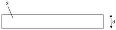
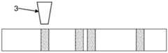
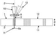
도 1 은 인쇄회로기판 제조에서 접촉요소로서 정해진, 기판 (2) 을 갖는 인터포저 (1) 안으로 다수의 관통 개구부를 도입할 때의 개별적인 방법단계들을 나타낸다. 이를 위해, 레이저 광선 (3) 은 기판 (2) 의 표면 쪽으로 지향된다. 기판 (2) 은 본질적인 재료 부분으로서 보로알루미노규산염을 구비하는데, 왜냐하면 이렇게 온도팽창을 규소의 온도팽창과 비슷하게 보장하기 위해서이다. 이때, 기판 (2) 의 재료 두께 (d) 는 50 ㎛ 과 500 ㎛ 사이이다. 이때, 레이저 광선 (3) 의 작용 기간은 매우 짧게 선택되고, 따라서 기판 재료의 본질적인 관통하는 파괴 또는 리세스가 발생하지 않으면서 상기 레이저 광선의 광선축 둘레로 동심적으로 기판 (2) 의 개질만 생긴다. 특히, 상기 작용 기간은 단일 펄스에 제한된다. 이를 위해, 파장을 갖는 레이저가 작동되고, 상기 파장에 대해 기판 (2) 이 투명하다. 이렇게 개질된 영역 (4) 은 도 1b 에 도시된다. 도 1c 에 도시된 다음 방법단계에서는, 도시되지 않은 에칭시키는 액체 또는 에칭시키는 기체의 작용에 근거하여, 먼저 레이저 광선 (3) 을 통해 개질을 거친 기판 (2) 의 영역들 (4) 에서는 이방성 재료 제거가 발생한다. 이를 통해, 원통형 작용 구역을 따라서 기판 (2) 안의 관통 개구부로서의 리세스 (5) 가 생긴다.Figure 1 shows the individual method steps when introducing a plurality of through openings into the
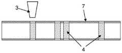
도 2 에서는 동일한 방법의 변경이 기술되고, 상기 변경에 있어서는, 도 2 b 에 도시된 레이저 광선 (3) 을 통한 개질 후, 도 2c 에서 알아볼 수 있는 바와 같이 평평한 금속층 (6) 이 기판 (2) 에 제공된다. 개질된 영역 (4) 에서의 이방성 재료 제거를 통해, 도 2d 에 도시된 다음 방법단계에서는 금속층 (6) 에 의해 일면이 폐쇄된 리세스들 (5) 이 생기고, 상기 리세스들은 추후의 접촉을 위한 베이스를 형성한다.2, a modification of the same method is described. In this modification, after the modification with the
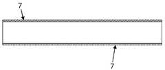
상기 방법의 그 밖의 변형은 도 3 에 도시된다. 이때, 기판 (2) 은 레이저 광선 (3) 을 이용한 레이저 가공 전에 도 3b 에 도시된 에칭 레지스트 (7) 로 코팅된다. 레이저 광선 (3) 의 작용에 근거하여, 점 모양의 작용 구역에서 동시에 에칭 레지스트 (7) 의 제거 및 그 아래에 놓여 있는 기판 (2) 의 영역의 개질이 발생하고, 이는 도 3c 에서 알아볼 수 있다. 이렇게, 기판 (2) 의 표면의 개질되지 않은 영역들은 후속 에칭공정에서의 원하지 않은 작용으로부터 보호되고, 상기 에칭공정을 통해, 도 3d 에 도시된 바와 같이, 이방성 재료 제거는 액체 에칭 방법을 통해 수행되고, 상응하는 리세스들 (5) 이 기판 (2) 안에 생긴다. 이른바 스트리핑 방법 (stripping method) 을 통해, 도 3e 에 도시된 바와 같이, 상기 에칭 방법의 종료 후 없어도 되는 에칭 레지스트 (7) 가 제거된다.Another modification of the method is shown in Fig. At this time, the
도 4 및 도 5 를 근거로, 하기에서는 기판 (2) 의 상기 레이저 가공 동안의 본질적인 효과가 상세히 설명된다. 이때, 단일 펄스 (P) 동안의, 강도 의존형 초점 위치에 관한 것이다. 이때, 본 발명은, 레이저 광선 (3) 의 단일 펄스 (P) 의 강도 (I) 가 변함없는 것이 아니라, 도 5 에 도시된 바와 같이 상기 단일 펄스의 시간적 진행에 걸쳐 예컨대 정규 분포에 상응하여 최소값 (Ia) 으로부터 평균값 (Ib) 을 거쳐 최대값 (Ic) 까지 증가하는, 그리고 그 후 감소하는 강도를 갖는다는 인식에 근거를 두고 있다. 동시에, 가변적인 강도 (I) 에 근거하여, 시간적 진행 (t) 에 걸친 단일 펄스 (P) 와 관련하여, 특히 또한 투과성 매체 (8) 의, 굴절률이 변한다. 이를 통해, 레이저 가공 헤드 (10) 의 포커싱 광학 시스템에 의해 결정된 기하학적 초점 위치와 상관없이, 도 4a 내지 도 4c 에 도시된, 레이저 광선 (3) 의, 강도 의존형 초점 위치들 (9a, 9b, 9c) 도 변하고, 바람직하게는 초점 위치들 (9a, 9b, 9c) 은 단일 펄스의 펄스 기간 (t) 동안 적어도 30 ㎛ 만큼 레이저 광선 (3) 의 광선축 (Z) 의 방향으로 옮겨진다. 이 효과는 레이저 가공 헤드 (10 와 기판 (2) 사이에 배치된, 공기보다 큰, 강도 의존형 굴절률을 갖는, 예컨대 유리로 만들어진 투과성 매체 (8) 를 통해, 최대 강도 (Ic) 와 최소 강도 (Ia) 사이의 초점 위치들 (9a, 9c) 사이의 간격이 적어도 원하는 세로방향 연장부에 상응하도록, 즉 도입되어야 하는 리세스의 깊이에 상응하도록 또는 도시된 바와 같이 도입되어야 하는 관통 구멍의 경우 기판 (2) 의 재료 두께 (d) 에 상응하도록 강화된다. 즉, 강도 의존형 포커스 포인트 (9a, 9b, 9c) 는 기판 (2) 의 뒷면 (11) 에 대해 간격을 둔, 도 4a 에 도시된 위치로부터 출발하여 레이저 가공 헤드 (10) 의 방향으로 광선축 (Z) 을 따라서 이동하고, 이렇게 연속적 운동에 있어서 뒷면 (11) 과 레이저 가공 헤드 (10) 를 향한 정면 (12) 사이의 광선축 (Z) 을 따른 모든 위치에 도달하고, 따라서 추후에 도입되어야 하는 리세스들의 전체 주 연장부의 영역 안의 원하는 개질이 발생한다.Based on Figs. 4 and 5, the intrinsic effects of the
보충적으로, 도 4a 에는 추가적인 레이저 가공 헤드 (13) 가 암시적으로만 도시되고, 상기 추가적인 레이저 가공 헤드를 통해, 펄스형 레이저의 레이저 광선 (3) 은 레이저 가공 헤드 (10) 와 연결된, 연속 방출형 레이저원에 대해 보충적으로 선택적으로 투과성 매체 (8) 를 관통하여 또는 상기 투과성 매체를 우회하면서 기판 (2) 쪽으로 지향된다. 이를 통해, 도 5 에 도시된 레이저 광선 (3) 의 단일 펄스 (P) 의 강도 (I) 는 상응하여 상기 연속 방출형 레이저원의 강도를 통해 강화된다.In addition, in figure 4a an additional
Claims (31)
Translated fromKorean도입되어야 하는 리세스들 (5) 의 영역에서 상기 기판 (2) 의 두께는 2 mm 를 넘지 않고,
레이저 파장을 위한 상기 기판 (2) 의 기판 재료는 적어도 부분적으로 투명하고, 상기 레이저 광선 (3) 은 상기 광학 시스템에 의해 원래의 초점 거리 (f1) 를 가지도록 포커싱되고, 상기 레이저 광선 (3) 의 강도는 상기 레이저 광선 (3) 의 광선축 (Z) 을 따른 상기 기판 (2) 의 개질을 발생시키고, 하지만 관통하는 재료 제거를 초래하지 않고, 이를 통해 바로 다음 단계에서 이방성 (anisotropic) 재료 제거는 먼저 상기 레이저 광선 (3) 에 의한 개질을 거친 그러한 영역들에서 수행되고, 따라서 리세스 (5) 가 상기 기판 (2) 안에 도입되고,
상기 레이저 광선 (3) 은, 단일 펄스 (P) 의 펄스 기간 (t) 내에서 비선형 (non-linear) 셀프 포커싱 (self-focusing) 을 통하여 상기 원래의 초점 거리 (f1) 와 상이한 초점 거리 (f2) 를 갖는, 상기 동일한 광학 시스템을 통해 포커싱되고,
펄스형 레이저 (pulsed laser) 의 강도가 단일 펄스와 관련하여 상기 단일 펄스의 시간적 진행에 걸쳐 최대값까지 증가하는, 그리고 그 후 감소하는 강도를 가지고, 이때 광학 시스템의 초점 거리는, 포커싱 광학 시스템에 의해 결정된 기하학적 초점위치와 상관없이 강도에 의존하여 조절 가능하고,
상기 초점 거리 (f2) 와 상기 원래의 초점 거리 (f1) 사이의 차이는 상기 도입되어야 하는 리세스 (5) 의 영역에서의 상기 기판 (2) 의 두께보다 큰 것을 특징으로 하는, 기판 안에 다수의 리세스를 도입하기 위한 방법.1. A method for introducing a plurality of recesses (5) into a substrate (2) by an optical system that irradiates a pulsed laser beam (3) having a pulse period (t)
The thickness of the substrate 2 in the region of the recesses 5 to be introduced does not exceed 2 mm,
The substrate material of the substrate 2 for the laser wavelength is at least partially transparent and the laser beam 3 is focused by the optical system to have the original focal length f1, The intensity of the laser beam 3 causes the modification of the substrate 2 along the optical axis Z of the laser beam 3 but does not result in the removal of material passing therethrough so that anisotropic material removal Is first performed in such areas modified by the laser beam 3 so that recesses 5 are introduced into the substrate 2,
The laser beam 3 is focused by non-linear self-focusing within a pulse period t of a single pulse P at a focal distance f2 that is different from the original focal distance f1 ), Which is focused through the same optical system,
Wherein the intensity of the pulsed laser increases with time to a maximum value over a temporal course of the single pulse with respect to a single pulse and thereafter decreases with the focal distance of the optical system being adjusted by the focusing optical system Irrespective of the determined geometrical focal position, is adjustable depending on the intensity,
Characterized in that the difference between the focal distance (f2) and the original focal distance (f1) is greater than the thickness of the substrate (2) in the region of the recess (5) A method for introducing a recess.
상기 초점 거리 (f2) 는 상기 원래의 초점 거리 (f1) 보다 작은 것을 특징으로 하는 방법.The method according to claim 1,
Wherein the focal length f2 is less than the original focal length f1.
상기 기판 (2) 은 본질적인 재료 부분으로서 유리, 사파이어 및/또는 규소를 구비하는 것을 특징으로 하는, 기판 안에 다수의 리세스를 도입하기 위한 방법.The method according to claim 1,
Characterized in that the substrate (2) comprises glass, sapphire and / or silicon as an integral part of the material.
상기 이방성 재료 제거는 불화수소산 안에서 에칭을 통해 실행되는 것을 특징으로 하는, 기판 안에 다수의 리세스를 도입하기 위한 방법.The method according to claim 1,
Wherein the anisotropic material removal is performed through etching in hydrofluoric acid. ≪ RTI ID = 0.0 > 11. < / RTI >
상기 기판 (2) 은 상기 레이저 광선 (3) 의 조사 전에 적어도 일면이 에칭 레지스트 (7) 로 코팅되는 것을 특징으로 하는, 기판 안에 다수의 리세스를 도입하기 위한 방법.The method according to claim 1,
Characterized in that the substrate (2) is coated with at least one side of the etching resist (7) before irradiation of the laser beam (3).
상기 기판 (2) 은 상기 레이저 광선 (3) 의 조사 전에 에칭 레지스트 (7) 로 적어도 하나의 표면에 평평하게 코팅되고, 레이저 광선 (3) 의 작용을 통해 동시에 점 모양의 작용 구역에서 상기 에칭 레지스트 (7) 가 제거되고, 적어도 하나의 표면에서 상기 기판 (2) 안의 개질이 발생되는 것을 특징으로 하는, 기판 안에 다수의 리세스를 도입하기 위한 방법.The method according to claim 6,
The substrate 2 is coated flat on at least one surface with an etching resist 7 prior to the irradiation of the laser beam 3 and is applied simultaneously to the etching resist 7 in the point- (7) is removed and a modification in the substrate (2) occurs at at least one surface.
상기 에칭 레지스트 (7) 는 이방성 재료 제거 후 상기 기판 (2) 의 표면에서 제거되는 것을 특징으로 하는, 기판 안에 다수의 리세스를 도입하기 위한 방법.The method according to claim 6,
Characterized in that the etching resist (7) is removed from the surface of the substrate (2) after removal of the anisotropic material.
상기 기판 (2) 은 적어도 일면이 금속으로 코팅되는 것을 특징으로 하는, 기판 안에 다수의 리세스를 도입하기 위한 방법.The method according to claim 1,
Characterized in that the substrate (2) is coated on at least one side with a metal.
상기 개질 후, 적어도 개별적인, 리세스 (5) 및/또는 관통 개구부들을 덮는, 상기 기판의 적어도 일면에 금속으로 코팅하기 위한 평평한 금속층 (6) 이 상기 기판 (2) 에 제공되고, 상기 리세스 (5) 및/또는 관통 개구부들은 상기 금속층 (6) 이 상기 기판 (2) 에 제공된 후에 뒤따라 도입되어야 하고, 다음 단계에서, 개질된 영역들 (4) 이 제거되고, 따라서 상기 금속층 (6) 에 의해 일면이 폐쇄된 리세스들 (5) 이 만들어지는 것을 특징으로 하는, 기판 안에 다수의 리세스를 도입하기 위한 방법.10. The method of claim 9,
After the modification, a flat metal layer (6) is provided on the substrate (2) for coating with at least one surface of the substrate, at least one of which covers the recesses (5) and / or through openings, 5 and / or through openings must be introduced after the metal layer 6 has been provided to the substrate 2, and in the next step, the modified regions 4 are removed and therefore the metal layer 6 Characterized in that a plurality of recesses (5) are made with one side closed.
상기 광학 시스템의 개구수 (numerical aperture, NA) 는 0.3 보다 큰 것을 특징으로 하는, 기판 안에 다수의 리세스를 도입하기 위한 방법.The method according to claim 1,
Wherein the numerical aperture (NA) of the optical system is greater than 0.3. ≪ RTI ID = 0.0 > 11. < / RTI >
상기 레이저 광선 (3) 은 먼저 투과성 매체 (transmissive medium, 8) 를 관통하여 지향되고, 상기 투과성 매체 (8) 는 공기보다 큰, 강도 의존형 (intensity dependent) 굴절률을 갖는 것을 특징으로 하는, 기판 안에 다수의 리세스를 도입하기 위한 방법.The method according to claim 1,
Characterized in that the laser beam (3) is first directed through a transmissive medium (8) and the transmissive medium (8) has an intensity dependent refractive index that is greater than air. Of the recesses.
상기 레이저 광선 (3) 은 상기 광학 시스템의 레이저 가공 헤드의 포커싱 광학 시스템 및 공기보다 큰 강도 의존형 굴절률 (n2) 을 갖는, 상기 레이저 광선 (3) 의 파장에 대해 상기 광학 시스템의 투과성 매체를 관통하여 지향되는 것을 특징으로 하는, 기판 안에 다수의 리세스를 도입하기 위한 방법.The method according to claim 1,
Characterized in that the laser beam (3) is passed through a transmissive medium of the optical system with respect to the wavelength of the laser beam (3), having a focusing optical system of the laser processing head of the optical system and an intensity- ≪ / RTI > wherein the plurality of recesses are oriented relative to one another.
상기 투과성 매체는 본질적인 재료 부분으로서 사파이어를 구비하는 것을 특징으로 하는, 기판 안에 다수의 리세스를 도입하기 위한 방법.13. The method of claim 12,
Characterized in that the transmissive medium comprises sapphire as an intrinsic material portion.
상기 레이저 광선 (3) 은 상기 광학 시스템으로부터 반대쪽을 향하는 상기 기판 (2) 의 뒷면 (11) 에 가까운 초점 거리 (f1) 를 갖는 포커스 포인트 (9a) 로 지향되는 것을 특징으로 하는, 기판 안에 다수의 리세스를 도입하기 위한 방법.The method according to claim 1,
Characterized in that the laser beam (3) is directed to a focus point (9a) with a focal distance (f1) close to the backside (11) of the substrate (2) facing away from the optical system A method for introducing a recess.
상기 레이저 광선 (3) 은 단일 펄스 (P) 의 펄스 기간 (t) 동안 각각의 포커스 포인트 (9a, 9b, 9c) 로 지향되는 것을 특징으로 하는, 기판 안에 다수의 리세스를 도입하기 위한 방법.16. The method of claim 15,
Characterized in that the laser beam (3) is directed to a respective focus point (9a, 9b, 9c) during a pulse period (t) of a single pulse (P).
각각의 포커스 포인트 (9a, 9b, 9c) 는 단일 펄스의 펄스 기간 (t) 동안 적어도 30 ㎛ 만큼 상기 레이저 광선 (3) 의 상기 광선축 (Z) 의 방향으로 옮겨지는 것을 특징으로 하는, 기판 안에 다수의 리세스를 도입하기 위한 방법.16. The method of claim 15,
Characterized in that each focus point (9a, 9b, 9c) is transferred in the direction of the ray axis (Z) of the laser beam (3) by at least 30 [mu] A method for introducing multiple recesses.
상기 레이저 광선 (3) 이 상기 기판 (2) 에 작용하는 동안, 상기 기판 (2) 은 상기 레이저 광선 (3) 에 대해 상대적으로 그리고/또는 레이저 가공 헤드 (10) 에 대해 상대적으로 광선축 (Z) 의 방향으로 중단 없이 움직여지는 것을 특징으로 하는, 기판 안에 다수의 리세스를 도입하기 위한 방법.The method according to claim 1,
While the laser beam 3 is acting on the substrate 2 the substrate 2 is moved relative to the laser processing head 10 relative to the laser beam 3 and / ) In a direction perpendicular to the direction of movement of the substrate.
상기 광학 시스템이 균일한 상대속도로 상기 기판 (2) 에 대해 상대적으로 움직여짐으로써 다수의 리세스 (5) 가 만들어지는 것을 특징으로 하는 방법.The method according to claim 1,
Characterized in that the optical system is moved relative to the substrate (2) at a uniform relative speed to create a plurality of recesses (5).
상기 레이저 광선 (3) 을 통해 추가적으로 표면 영역도 제거되는 것을 특징으로 하는, 기판 안에 다수의 리세스를 도입하기 위한 방법.The method according to claim 1,
Characterized in that an additional surface area is also removed through the laser beam (3).
상기 레이저 광선 (3) 의 상기 펄스 기간 (t) 은 50 ps 보다 적은 것을 특징으로 하는 방법.The method according to claim 1,
Characterized in that the pulse duration (t) of the laser beam (3) is less than 50 ps.
펄스형 레이저의 상기 레이저 광선 (3) 은 투과성 매체 (8) 를 통해, 그리고 연속 방출형 레이저의 레이저 광선은 상기 투과성 매체 (8) 를 통해 또는 상기 투과성 매체 (8) 를 우회하여 상기 기판 (2) 으로 지향되는 것을 특징으로 하는, 기판 안에 다수의 리세스를 도입하기 위한 방법.The method according to claim 1,
The laser beam 3 of the pulsed laser is transmitted through the transmissive medium 8 and the laser beam of the continuous emission laser is transmitted through the transmissive medium 8 or by the substrate 2 ≪ / RTI > wherein the plurality of recesses are oriented in a first direction.
상기 이방성 재료 제거를 통해 외부 표면들 (11, 12) 사이의 관통 개구부로서 상기 리세스 (5) 는 상기 기판 (2) 안에 도입되는 것을 특징으로 하는, 기판 안에 다수의 리세스를 도입하기 위한 방법.The method according to claim 1,
Characterized in that said recesses (5) are introduced into said substrate (2) as through openings between said outer surfaces (11, 12) through said anisotropic material removal, characterized in that a plurality of recesses .
상기 레이저 광선 (3) 이 투과성 매체 (8) 를 관통하여 상기 기판 (2) 으로 굴절될 수 있을 정도로 상기 레이저 가공 헤드 (10) 와 상기 기판 (2) 사이에, 공기보다 큰 강도 의존형 굴절률을 갖는, 평면 평행하는 (plane-parallel) 상기 투과성 매체 (8) 가 배치되고,
펄스형 레이저 (pulsed laser) 의 강도가 단일 펄스와 관련하여 상기 단일 펄스의 시간적 진행에 걸쳐 최대값까지 증가하는, 그리고 그 후 감소하는 강도를 가지고, 이때 광학 시스템의 초점 거리는, 포커싱 광학 시스템에 의해 결정된 기하학적 초점위치와 상관없이 강도에 의존하여 조절 가능한 것을 특징으로 하는, 기판 안에 다수의 리세스를 도입하기 위한 장치.An apparatus comprising an optical system having a laser machining head (10) for refracting a laser beam (3) onto a substrate (2) to carry out the method according to claim 1,
Characterized in that there is provided between the laser processing head (10) and the substrate (2) such that the laser beam (3) penetrates through the transmissive medium (8) , Said plane-parallel transmissive medium (8) being arranged,
Wherein the intensity of the pulsed laser increases with time to a maximum value over a temporal course of the single pulse with respect to a single pulse and thereafter decreases with the focal distance of the optical system being adjusted by the focusing optical system Characterized in that it is adjustable in dependence on the intensity irrespective of the determined geometrical focus position.
상기 레이저 광선 (3) 은 상기 레이저 가공 헤드 (10) 로부터 반대쪽을 향하는 상기 기판 (2) 의 뒷면 (11) 에 간격을 두고 포커스 포인트 (9a, 9b, 9c) 쪽으로 굴절될 수 있는 것을 특징으로 하는, 기판 안에 다수의 리세스를 도입하기 위한 장치.25. The method of claim 24,
Characterized in that the laser beam (3) can be refracted towards the focus points (9a, 9b, 9c) at intervals on the backside (11) of the substrate (2) facing away from the laser machining head And a plurality of recesses in the substrate.
상기 레이저 광선 (3) 의 펄스 기간 (t) 은 50 ps 보다 적은 것을 특징으로 하는, 기판 안에 다수의 리세스를 도입하기 위한 장치.25. The method of claim 24,
Characterized in that the pulse duration (t) of the laser beam (3) is less than 50 ps.
상기 투과성 매체 (8) 는 유리, 및/또는 사파이어로 구성되는 것을 특징으로 하는, 레이저 가공 헤드를 구비하는, 기판 안에 다수의 리세스를 도입하기 위한 장치.25. The method of claim 24,
Characterized in that the transmissive medium (8) is composed of glass and / or sapphire.
상기 투과성 매체 (8) 는 상기 레이저 가공 헤드 (10) 와 연결되고, 상기 레이저 가공 헤드와 함께 움직일 수 있게 배치되는 것을 특징으로 하는, 기판 안에 다수의 리세스를 도입하기 위한 장치.25. The method of claim 24,
Characterized in that the transmissive medium (8) is connected to the laser machining head (10) and is arranged movably with the laser machining head.
상기 장치는 펄스형 레이저와 연결되고, 연속 방출형 레이저와 연결되는 것을 특징으로 하는, 기판 안에 다수의 리세스를 도입하기 위한 장치.25. The method of claim 24,
Characterized in that the device is connected to a pulsed laser and to a continuous emission laser.
상기 광학 시스템의 개구수 (NA) 는 0.3 보다 큰 것을 특징으로 하는, 기판 안에 다수의 리세스를 도입하기 위한 장치.25. The method of claim 24,
Wherein the numerical aperture (NA) of the optical system is greater than 0.3.
Applications Claiming Priority (5)
| Application Number | Priority Date | Filing Date | Title |
|---|---|---|---|
| DE201310103370DE102013103370A1 (en) | 2013-04-04 | 2013-04-04 | Method for introducing perforations into a glass substrate and a glass substrate produced in this way |
| DE102013103370.9 | 2013-04-04 | ||
| DE102013112033 | 2013-10-31 | ||
| DE102013112033.4 | 2013-10-31 | ||
| PCT/DE2014/100118WO2014161534A2 (en) | 2013-04-04 | 2014-04-03 | Method and device for providing through-openings in a substrate and a substrate produced in said manner |
Publications (2)
| Publication Number | Publication Date |
|---|---|
| KR20150128802A KR20150128802A (en) | 2015-11-18 |
| KR101857335B1true KR101857335B1 (en) | 2018-05-11 |
Family
ID=50792337
Family Applications (1)
| Application Number | Title | Priority Date | Filing Date |
|---|---|---|---|
| KR1020157027412AActiveKR101857335B1 (en) | 2013-04-04 | 2014-04-03 | Method and device for providing through-openings in a substrate and a substrate produced in said manner |
Country Status (9)
| Country | Link |
|---|---|
| US (3) | US10610971B2 (en) |
| EP (1) | EP2964417B1 (en) |
| JP (1) | JP6186016B2 (en) |
| KR (1) | KR101857335B1 (en) |
| CN (1) | CN105102177B (en) |
| ES (1) | ES2908956T3 (en) |
| LT (1) | LT2964417T (en) |
| MY (1) | MY178429A (en) |
| WO (1) | WO2014161534A2 (en) |
Families Citing this family (75)
| Publication number | Priority date | Publication date | Assignee | Title |
|---|---|---|---|---|
| JP6121901B2 (en) | 2010-07-12 | 2017-04-26 | ロフィン−シナー テクノロジーズ インコーポレーテッド | Material processing by laser filament formation |
| WO2014079478A1 (en) | 2012-11-20 | 2014-05-30 | Light In Light Srl | High speed laser processing of transparent materials |
| EP2754524B1 (en) | 2013-01-15 | 2015-11-25 | Corning Laser Technologies GmbH | Method of and apparatus for laser based processing of flat substrates being wafer or glass element using a laser beam line |
| EP2781296B1 (en) | 2013-03-21 | 2020-10-21 | Corning Laser Technologies GmbH | Device and method for cutting out contours from flat substrates using a laser |
| CN105189024B (en)* | 2013-04-04 | 2018-01-30 | Lpkf激光电子股份公司 | Method and apparatus for separating substrates |
| US9102011B2 (en) | 2013-08-02 | 2015-08-11 | Rofin-Sinar Technologies Inc. | Method and apparatus for non-ablative, photoacoustic compression machining in transparent materials using filamentation by burst ultrafast laser pulses |
| US10017410B2 (en) | 2013-10-25 | 2018-07-10 | Rofin-Sinar Technologies Llc | Method of fabricating a glass magnetic hard drive disk platter using filamentation by burst ultrafast laser pulses |
| US10005152B2 (en) | 2013-11-19 | 2018-06-26 | Rofin-Sinar Technologies Llc | Method and apparatus for spiral cutting a glass tube using filamentation by burst ultrafast laser pulses |
| US9517929B2 (en) | 2013-11-19 | 2016-12-13 | Rofin-Sinar Technologies Inc. | Method of fabricating electromechanical microchips with a burst ultrafast laser pulses |
| US10252507B2 (en) | 2013-11-19 | 2019-04-09 | Rofin-Sinar Technologies Llc | Method and apparatus for forward deposition of material onto a substrate using burst ultrafast laser pulse energy |
| US11053156B2 (en) | 2013-11-19 | 2021-07-06 | Rofin-Sinar Technologies Llc | Method of closed form release for brittle materials using burst ultrafast laser pulses |
| US10144088B2 (en) | 2013-12-03 | 2018-12-04 | Rofin-Sinar Technologies Llc | Method and apparatus for laser processing of silicon by filamentation of burst ultrafast laser pulses |
| US11556039B2 (en) | 2013-12-17 | 2023-01-17 | Corning Incorporated | Electrochromic coated glass articles and methods for laser processing the same |
| US20150165560A1 (en) | 2013-12-17 | 2015-06-18 | Corning Incorporated | Laser processing of slots and holes |
| US9701563B2 (en) | 2013-12-17 | 2017-07-11 | Corning Incorporated | Laser cut composite glass article and method of cutting |
| US9850160B2 (en) | 2013-12-17 | 2017-12-26 | Corning Incorporated | Laser cutting of display glass compositions |
| US10293436B2 (en) | 2013-12-17 | 2019-05-21 | Corning Incorporated | Method for rapid laser drilling of holes in glass and products made therefrom |
| US9815730B2 (en) | 2013-12-17 | 2017-11-14 | Corning Incorporated | Processing 3D shaped transparent brittle substrate |
| US9676167B2 (en) | 2013-12-17 | 2017-06-13 | Corning Incorporated | Laser processing of sapphire substrate and related applications |
| US10442719B2 (en) | 2013-12-17 | 2019-10-15 | Corning Incorporated | Edge chamfering methods |
| US9938187B2 (en) | 2014-02-28 | 2018-04-10 | Rofin-Sinar Technologies Llc | Method and apparatus for material processing using multiple filamentation of burst ultrafast laser pulses |
| CN106687419A (en) | 2014-07-08 | 2017-05-17 | 康宁股份有限公司 | Methods and apparatuses for laser processing materials |
| KR20170028943A (en) | 2014-07-14 | 2017-03-14 | 코닝 인코포레이티드 | System for and method of processing transparent materials using laser beam focal lines adjustable in length and diameter |
| JP6788571B2 (en)* | 2014-07-14 | 2020-11-25 | コーニング インコーポレイテッド | Interface blocks, systems and methods for cutting transparent substrates within a wavelength range using such interface blocks. |
| EP3169479B1 (en) | 2014-07-14 | 2019-10-02 | Corning Incorporated | Method of and system for arresting incident crack propagation in a transparent material |
| CN208586209U (en) | 2014-07-14 | 2019-03-08 | 康宁股份有限公司 | A system for forming contoured multiple defects in a workpiece |
| US9757815B2 (en) | 2014-07-21 | 2017-09-12 | Rofin-Sinar Technologies Inc. | Method and apparatus for performing laser curved filamentation within transparent materials |
| US10047001B2 (en) | 2014-12-04 | 2018-08-14 | Corning Incorporated | Glass cutting systems and methods using non-diffracting laser beams |
| JP6104354B2 (en)* | 2014-12-16 | 2017-03-29 | 旭硝子株式会社 | Through-hole forming method, through-hole forming apparatus, and method for manufacturing glass substrate having through-hole |
| CN107406293A (en) | 2015-01-12 | 2017-11-28 | 康宁股份有限公司 | The substrate through heat tempering is cut by laser using Multiphoton Absorbtion method |
| EP3102358A4 (en) | 2015-01-13 | 2017-10-25 | Rofin-Sinar Technologies, Inc. | Method and system for scribing brittle material followed by chemical etching |
| HUE055461T2 (en) | 2015-03-24 | 2021-11-29 | Corning Inc | Laser cutting and processing of display glass compositions |
| JP2018516215A (en) | 2015-03-27 | 2018-06-21 | コーニング インコーポレイテッド | Gas permeable window and manufacturing method thereof |
| TW201704177A (en)* | 2015-06-10 | 2017-02-01 | 康寧公司 | Methods of etching glass substrates and glass substrates |
| JP7082042B2 (en) | 2015-07-10 | 2022-06-07 | コーニング インコーポレイテッド | A method for continuously forming holes in a flexible substrate sheet and related products. |
| WO2017034969A1 (en)* | 2015-08-21 | 2017-03-02 | Corning Incorporated | Methods of continuous fabrication of features in flexible substrate webs and products relating to the same |
| CN107922259B (en) | 2015-09-04 | 2021-05-07 | Agc株式会社 | Method for producing glass plate, method for producing glass article, and apparatus for producing glass article |
| US10410883B2 (en) | 2016-06-01 | 2019-09-10 | Corning Incorporated | Articles and methods of forming vias in substrates |
| US10794679B2 (en) | 2016-06-29 | 2020-10-06 | Corning Incorporated | Method and system for measuring geometric parameters of through holes |
| JP6996508B2 (en) | 2016-09-01 | 2022-01-17 | Agc株式会社 | Manufacturing method of glass articles and glass articles |
| US10730783B2 (en) | 2016-09-30 | 2020-08-04 | Corning Incorporated | Apparatuses and methods for laser processing transparent workpieces using non-axisymmetric beam spots |
| EP3529214B1 (en) | 2016-10-24 | 2020-12-23 | Corning Incorporated | Substrate processing station for laser-based machining of sheet-like glass substrates |
| EP3542396A4 (en)* | 2016-11-18 | 2020-06-17 | Samtec Inc. | Filling materials and methods of filling through holes of a substrate |
| CN110291051B (en) | 2017-02-21 | 2022-04-29 | Agc株式会社 | Glass plate and method for manufacturing glass plate |
| JP6531878B2 (en) | 2017-02-21 | 2019-06-19 | Agc株式会社 | Glass plate and method of manufacturing glass plate |
| WO2018162385A1 (en)* | 2017-03-06 | 2018-09-13 | Lpkf Laser & Electronics Ag | Method for producing at least one recess in a material by means of electromagnetic radiation and subsequent etching process |
| TWI681445B (en)* | 2017-03-06 | 2020-01-01 | 德商Lpkf雷射暨電子股份公司 | Method for producing a technical mask and method for patterned material application and/or removal by means of a reusable mask |
| EP3592501B1 (en) | 2017-03-06 | 2021-10-06 | LPKF Laser & Electronics AG | Method for producing a technical mask |
| KR102260931B1 (en)* | 2017-05-15 | 2021-06-04 | 엘피케이에프 레이저 앤드 일렉트로닉스 악티엔게젤샤프트 | Method for processing substrates using laser induced deep reactive etching, in particular for separation |
| US10580725B2 (en) | 2017-05-25 | 2020-03-03 | Corning Incorporated | Articles having vias with geometry attributes and methods for fabricating the same |
| US11078112B2 (en)* | 2017-05-25 | 2021-08-03 | Corning Incorporated | Silica-containing substrates with vias having an axially variable sidewall taper and methods for forming the same |
| US11156774B2 (en)* | 2017-10-04 | 2021-10-26 | Lpkf Laser & Electronics Ag | Optical component and method for the production thereof |
| KR102538306B1 (en)* | 2017-11-10 | 2023-06-07 | 엘피케이에프 레이저 앤드 일렉트로닉스 에스이 | Semiconductor wafer integration method and device |
| US12180108B2 (en) | 2017-12-19 | 2024-12-31 | Corning Incorporated | Methods for etching vias in glass-based articles employing positive charge organic molecules |
| JP7407499B2 (en)* | 2017-12-26 | 2024-01-04 | 株式会社ディスコ | Method for forming recesses or through holes, method for forming electrodes |
| US11554984B2 (en) | 2018-02-22 | 2023-01-17 | Corning Incorporated | Alkali-free borosilicate glasses with low post-HF etch roughness |
| WO2019191621A1 (en) | 2018-03-30 | 2019-10-03 | Samtec, Inc. | Electrically conductive vias and methods for producing same |
| DE102020100848B4 (en) | 2019-01-29 | 2023-07-27 | Lpkf Laser & Electronics Aktiengesellschaft | Process for microstructuring a glass substrate using laser radiation |
| JP7230650B2 (en) | 2019-04-05 | 2023-03-01 | Tdk株式会社 | Inorganic material substrate processing method, device, and device manufacturing method |
| DE102019111634A1 (en)* | 2019-05-06 | 2020-11-12 | Lpkf Laser & Electronics Ag | Process for the production of microstructures in a glass substrate |
| KR102771848B1 (en)* | 2019-05-13 | 2025-02-21 | 엘피케이에프 레이저 앤드 일렉트로닉스 에스이 | Method for manufacturing a display having a carrier substrate, a carrier substrate manufactured according to the method, and a cover glass intended for a flexible display |
| WO2021008700A1 (en) | 2019-07-17 | 2021-01-21 | Scrona Ag | Inkjet print head with contamination robustness |
| EP3969285B1 (en) | 2019-07-17 | 2024-04-24 | Scrona AG | Electrohydrodynamic print head with structured feed layer |
| US12100647B2 (en) | 2019-09-30 | 2024-09-24 | Samtec, Inc. | Electrically conductive vias and methods for producing same |
| DE102019217466A1 (en)* | 2019-11-12 | 2021-05-12 | Lpkf Laser & Electronics Ag | Glass reaction vessels, manufacturing processes and methods for analysis |
| DE102021100144A1 (en) | 2020-01-09 | 2021-07-15 | Lpkf Laser & Electronics Aktiengesellschaft | Process for processing a glass |
| KR102311023B1 (en)* | 2020-05-26 | 2021-10-08 | 윤창희 | Double material transfer type plasma etching plate with improved processing efficiency |
| DE102020114195A1 (en)* | 2020-05-27 | 2021-12-02 | Lpkf Laser & Electronics Aktiengesellschaft | Method for making a recess in a substrate |
| EP4296244A1 (en) | 2022-06-21 | 2023-12-27 | LPKF Laser & Electronics SE | Substrate carrier made of glass for processing a substrate and a method for producing the same |
| DE102022116784A1 (en) | 2022-07-05 | 2024-01-11 | Lpkf Laser & Electronics Aktiengesellschaft | Micromechanical glass comb structure and associated process and use |
| DE102022116783B3 (en) | 2022-07-05 | 2023-09-14 | Lpkf Laser & Electronics Aktiengesellschaft | Glass microstructure, micro-mechanics and related uses |
| DE102022127259A1 (en) | 2022-10-18 | 2024-04-18 | Lpkf Laser & Electronics Aktiengesellschaft | Method and device for imaging a beam onto an object and method for making an opening in a workpiece by means of this method |
| DE102022130976B3 (en) | 2022-11-23 | 2023-11-30 | Lpkf Laser & Electronics Aktiengesellschaft | Monolithic membrane made of glass, double vertical membrane arrangement, micromechanical spring structure and associated manufacturing process |
| KR102559949B1 (en)* | 2022-12-15 | 2023-07-26 | 주식회사 에프엠에스 | Method of forming a hole through a glass substrate and method of forming a metal plug |
| DE102024105120A1 (en) | 2024-02-23 | 2025-08-28 | Lpkf Laser & Electronics Se | Method for integrating and/or processing at least one substrate and substrate stack |
Citations (5)
| Publication number | Priority date | Publication date | Assignee | Title |
|---|---|---|---|---|
| JP2001242495A (en)* | 2000-02-28 | 2001-09-07 | Inst Of Physical & Chemical Res | Short pulse laser beam pulse width compression method |
| DE10154361A1 (en)* | 2001-11-06 | 2003-05-15 | Univ Albert Ludwigs Freiburg | Rapid prototyping process used in microstructures comprises applying etch-resistant coating to substrate, selectively removing the coating using a laser beam to produce at least one exposed region, and etching the exposed region |
| JP2005288501A (en)* | 2004-03-31 | 2005-10-20 | Hokkaido Univ | Laser processing method and apparatus |
| JP2011222700A (en)* | 2010-04-08 | 2011-11-04 | Fujikura Ltd | Method for forming fine structure, laser irradiation device, and substrate |
| WO2012014718A1 (en)* | 2010-07-26 | 2012-02-02 | 浜松ホトニクス株式会社 | Method for manufacturing interposer |
Family Cites Families (32)
| Publication number | Priority date | Publication date | Assignee | Title |
|---|---|---|---|---|
| JPS59127983A (en)* | 1982-12-24 | 1984-07-23 | Toshiba Corp | Laser working device |
| EP0286855A1 (en)* | 1987-04-15 | 1988-10-19 | BBC Brown Boveri AG | Process for etching moats in a silicon substrate |
| JPH02303148A (en)* | 1989-05-18 | 1990-12-17 | Mitsubishi Electric Corp | Manufacture of aluminum nitride package |
| IL105925A (en)* | 1992-06-22 | 1997-01-10 | Martin Marietta Corp | Ablative process for printed circuit board technology |
| US5738757A (en)* | 1995-11-22 | 1998-04-14 | Northrop Grumman Corporation | Planar masking for multi-depth silicon etching |
| US6114240A (en) | 1997-12-18 | 2000-09-05 | Micron Technology, Inc. | Method for fabricating semiconductor components using focused laser beam |
| US7569794B2 (en)* | 2001-05-23 | 2009-08-04 | Osmotica Corp. | Laser drilling system and method |
| JP4418282B2 (en) | 2004-03-31 | 2010-02-17 | 株式会社レーザーシステム | Laser processing method |
| US7303977B2 (en)* | 2004-11-10 | 2007-12-04 | Intel Corporation | Laser micromachining method |
| US9138913B2 (en) | 2005-09-08 | 2015-09-22 | Imra America, Inc. | Transparent material processing with an ultrashort pulse laser |
| JP5232375B2 (en)* | 2006-10-13 | 2013-07-10 | アイシン精機株式会社 | Method for separating semiconductor light emitting device |
| JP5221007B2 (en)* | 2006-05-31 | 2013-06-26 | アイシン精機株式会社 | Light emitting diode chip and wafer split processing method |
| US20070298529A1 (en) | 2006-05-31 | 2007-12-27 | Toyoda Gosei, Co., Ltd. | Semiconductor light-emitting device and method for separating semiconductor light-emitting devices |
| JP2008288577A (en)* | 2007-04-18 | 2008-11-27 | Fujikura Ltd | Substrate processing method, through wiring substrate and method for manufacturing the same, and electronic component |
| JP2008288264A (en)* | 2007-05-15 | 2008-11-27 | Ntn Corp | Pattern correction method |
| JP2009176926A (en) | 2008-01-24 | 2009-08-06 | Fujikura Ltd | Penetration wiring board and manufacturing method thereof |
| TW201036508A (en) | 2009-03-17 | 2010-10-01 | High Conduction Scient Co Ltd | Double-faced conductive composite board and manufacturing method thereof |
| CN101571603A (en) | 2009-06-02 | 2009-11-04 | 中国科学院上海光学精密机械研究所 | Method for preparing micro-optical elements on quartz glass substrate using femtosecond laser |
| US20120234807A1 (en)* | 2009-12-07 | 2012-09-20 | J.P. Sercel Associates Inc. | Laser scribing with extended depth affectation into a workplace |
| JP5600427B2 (en)* | 2009-12-25 | 2014-10-01 | 株式会社フジクラ | Material substrate for through wiring board |
| KR101181719B1 (en)* | 2010-06-22 | 2012-09-19 | 한국과학기술원 | Substrate Dicing Method by Nano Void Array Formation using Femtosecond Pulse Lasers |
| DE102010025966B4 (en) | 2010-07-02 | 2012-03-08 | Schott Ag | Interposer and method for making holes in an interposer |
| JP6121901B2 (en)* | 2010-07-12 | 2017-04-26 | ロフィン−シナー テクノロジーズ インコーポレーテッド | Material processing by laser filament formation |
| WO2012094737A1 (en)* | 2011-01-10 | 2012-07-19 | UNIVERSITé LAVAL | Laser reinforced direct bonding of optical components |
| CN102513700B (en)* | 2011-11-03 | 2015-04-15 | 西安交通大学 | Method for forming three-dimensional micro spiral channel inside quartz glass by using femto-second laser |
| JP5938416B2 (en)* | 2011-11-04 | 2016-06-22 | 株式会社フジクラ | Method for manufacturing a substrate with fine holes |
| TW201343296A (en)* | 2012-03-16 | 2013-11-01 | Ipg Microsystems Llc | Laser scribing system and method with extended depth affectation into a workpiece |
| CN105246850B (en) | 2012-11-29 | 2018-01-30 | 康宁股份有限公司 | Pass through the method for laser damage and etching manufacture glassware |
| EP2781296B1 (en)* | 2013-03-21 | 2020-10-21 | Corning Laser Technologies GmbH | Device and method for cutting out contours from flat substrates using a laser |
| US20150034613A1 (en)* | 2013-08-02 | 2015-02-05 | Rofin-Sinar Technologies Inc. | System for performing laser filamentation within transparent materials |
| US9296646B2 (en) | 2013-08-29 | 2016-03-29 | Corning Incorporated | Methods for forming vias in glass substrates |
| US10144088B2 (en)* | 2013-12-03 | 2018-12-04 | Rofin-Sinar Technologies Llc | Method and apparatus for laser processing of silicon by filamentation of burst ultrafast laser pulses |
- 2014
- 2014-04-03KRKR1020157027412Apatent/KR101857335B1/enactiveActive
- 2014-04-03USUS14/781,599patent/US10610971B2/enactiveActive
- 2014-04-03WOPCT/DE2014/100118patent/WO2014161534A2/enactiveApplication Filing
- 2014-04-03JPJP2015561940Apatent/JP6186016B2/enactiveActive
- 2014-04-03MYMYPI2015703466Apatent/MY178429A/enunknown
- 2014-04-03LTLTEPPCT/DE2014/100118Tpatent/LT2964417T/enunknown
- 2014-04-03ESES14726069Tpatent/ES2908956T3/enactiveActive
- 2014-04-03EPEP14726069.9Apatent/EP2964417B1/enactiveActive
- 2014-04-03CNCN201480019446.7Apatent/CN105102177B/enactiveActive
- 2020
- 2020-02-24USUS16/798,453patent/US11618104B2/enactiveActive
- 2023
- 2023-02-28USUS18/175,557patent/US12365051B2/enactiveActive
Patent Citations (5)
| Publication number | Priority date | Publication date | Assignee | Title |
|---|---|---|---|---|
| JP2001242495A (en)* | 2000-02-28 | 2001-09-07 | Inst Of Physical & Chemical Res | Short pulse laser beam pulse width compression method |
| DE10154361A1 (en)* | 2001-11-06 | 2003-05-15 | Univ Albert Ludwigs Freiburg | Rapid prototyping process used in microstructures comprises applying etch-resistant coating to substrate, selectively removing the coating using a laser beam to produce at least one exposed region, and etching the exposed region |
| JP2005288501A (en)* | 2004-03-31 | 2005-10-20 | Hokkaido Univ | Laser processing method and apparatus |
| JP2011222700A (en)* | 2010-04-08 | 2011-11-04 | Fujikura Ltd | Method for forming fine structure, laser irradiation device, and substrate |
| WO2012014718A1 (en)* | 2010-07-26 | 2012-02-02 | 浜松ホトニクス株式会社 | Method for manufacturing interposer |
Also Published As
| Publication number | Publication date |
|---|---|
| KR20150128802A (en) | 2015-11-18 |
| CN105102177B (en) | 2018-02-27 |
| US20200189039A1 (en) | 2020-06-18 |
| MY178429A (en) | 2020-10-13 |
| JP2016517626A (en) | 2016-06-16 |
| US11618104B2 (en) | 2023-04-04 |
| EP2964417A2 (en) | 2016-01-13 |
| US20230201970A1 (en) | 2023-06-29 |
| WO2014161534A3 (en) | 2014-11-27 |
| CN105102177A (en) | 2015-11-25 |
| JP6186016B2 (en) | 2017-08-23 |
| US20160059359A1 (en) | 2016-03-03 |
| US10610971B2 (en) | 2020-04-07 |
| ES2908956T3 (en) | 2022-05-04 |
| WO2014161534A2 (en) | 2014-10-09 |
| EP2964417B1 (en) | 2022-01-12 |
| US12365051B2 (en) | 2025-07-22 |
| LT2964417T (en) | 2022-04-11 |
Similar Documents
| Publication | Publication Date | Title |
|---|---|---|
| KR101857335B1 (en) | Method and device for providing through-openings in a substrate and a substrate produced in said manner | |
| KR101857336B1 (en) | Method and device for separating a substrate | |
| KR102851778B1 (en) | Method for introducing at least one cutout or aperture into a sheetlike workpiece | |
| CN110382160B (en) | Method for opening at least one recess into a material by means of electromagnetic radiation and a subsequent etching process | |
| JP6181031B2 (en) | Method and apparatus for forward deposition on a substrate by energy transfer of burst ultrafast laser pulses | |
| CN103025478B (en) | Substrate processing method | |
| KR101940334B1 (en) | Laser processing method | |
| KR20130098167A (en) | Method for manufacturing light-absorbing substrate and method for manufacturing die for manufacturing light-absorbing substrate | |
| KR102640881B1 (en) | Systems and methods for drilling vias in transparent materials | |
| KR101207583B1 (en) | Laser processing method and apparatus using ultrasonic wave | |
| KR101094322B1 (en) | Laser processing apparatus and multi-layer substrate processing method using the same | |
| KR102191666B1 (en) | Method for processing transparent materials using spatio-temporally shaped pulsed-laser beam and Apparatus for the same |
Legal Events
| Date | Code | Title | Description |
|---|---|---|---|
| A201 | Request for examination | ||
| PA0105 | International application | Patent event date:20151002 Patent event code:PA01051R01D Comment text:International Patent Application | |
| PA0201 | Request for examination | ||
| PG1501 | Laying open of application | ||
| E902 | Notification of reason for refusal | ||
| PE0902 | Notice of grounds for rejection | Comment text:Notification of reason for refusal Patent event date:20170221 Patent event code:PE09021S01D | |
| E90F | Notification of reason for final refusal | ||
| PE0902 | Notice of grounds for rejection | Comment text:Final Notice of Reason for Refusal Patent event date:20170912 Patent event code:PE09021S02D | |
| E701 | Decision to grant or registration of patent right | ||
| PE0701 | Decision of registration | Patent event code:PE07011S01D Comment text:Decision to Grant Registration Patent event date:20180206 | |
| GRNT | Written decision to grant | ||
| PR0701 | Registration of establishment | Comment text:Registration of Establishment Patent event date:20180504 Patent event code:PR07011E01D | |
| PR1002 | Payment of registration fee | Payment date:20180504 End annual number:3 Start annual number:1 | |
| PG1601 | Publication of registration | ||
| PR1001 | Payment of annual fee | Payment date:20220425 Start annual number:5 End annual number:5 | |
| PR1001 | Payment of annual fee | Payment date:20230427 Start annual number:6 End annual number:6 | |
| PR1001 | Payment of annual fee | Payment date:20240423 Start annual number:7 End annual number:7 | |
| PR1001 | Payment of annual fee | Payment date:20250421 Start annual number:8 End annual number:8 |