KR101857249B1 - Patterning slit sheet assembly, apparatus for organic layer deposition, method for manufacturing organic light emitting display apparatus and organic light emitting display apparatus - Google Patents
Patterning slit sheet assembly, apparatus for organic layer deposition, method for manufacturing organic light emitting display apparatus and organic light emitting display apparatusDownload PDFInfo
- Publication number
- KR101857249B1 KR101857249B1KR1020110050842AKR20110050842AKR101857249B1KR 101857249 B1KR101857249 B1KR 101857249B1KR 1020110050842 AKR1020110050842 AKR 1020110050842AKR 20110050842 AKR20110050842 AKR 20110050842AKR 101857249 B1KR101857249 B1KR 101857249B1
- Authority
- KR
- South Korea
- Prior art keywords
- frame
- slit sheet
- evaporation source
- patterning slit
- region
- Prior art date
- Legal status (The legal status is an assumption and is not a legal conclusion. Google has not performed a legal analysis and makes no representation as to the accuracy of the status listed.)
- Expired - Fee Related
Links
Images


Classifications
- C—CHEMISTRY; METALLURGY
- C23—COATING METALLIC MATERIAL; COATING MATERIAL WITH METALLIC MATERIAL; CHEMICAL SURFACE TREATMENT; DIFFUSION TREATMENT OF METALLIC MATERIAL; COATING BY VACUUM EVAPORATION, BY SPUTTERING, BY ION IMPLANTATION OR BY CHEMICAL VAPOUR DEPOSITION, IN GENERAL; INHIBITING CORROSION OF METALLIC MATERIAL OR INCRUSTATION IN GENERAL
- C23C—COATING METALLIC MATERIAL; COATING MATERIAL WITH METALLIC MATERIAL; SURFACE TREATMENT OF METALLIC MATERIAL BY DIFFUSION INTO THE SURFACE, BY CHEMICAL CONVERSION OR SUBSTITUTION; COATING BY VACUUM EVAPORATION, BY SPUTTERING, BY ION IMPLANTATION OR BY CHEMICAL VAPOUR DEPOSITION, IN GENERAL
- C23C14/00—Coating by vacuum evaporation, by sputtering or by ion implantation of the coating forming material
- C23C14/04—Coating on selected surface areas, e.g. using masks
- C23C14/042—Coating on selected surface areas, e.g. using masks using masks
- C—CHEMISTRY; METALLURGY
- C23—COATING METALLIC MATERIAL; COATING MATERIAL WITH METALLIC MATERIAL; CHEMICAL SURFACE TREATMENT; DIFFUSION TREATMENT OF METALLIC MATERIAL; COATING BY VACUUM EVAPORATION, BY SPUTTERING, BY ION IMPLANTATION OR BY CHEMICAL VAPOUR DEPOSITION, IN GENERAL; INHIBITING CORROSION OF METALLIC MATERIAL OR INCRUSTATION IN GENERAL
- C23C—COATING METALLIC MATERIAL; COATING MATERIAL WITH METALLIC MATERIAL; SURFACE TREATMENT OF METALLIC MATERIAL BY DIFFUSION INTO THE SURFACE, BY CHEMICAL CONVERSION OR SUBSTITUTION; COATING BY VACUUM EVAPORATION, BY SPUTTERING, BY ION IMPLANTATION OR BY CHEMICAL VAPOUR DEPOSITION, IN GENERAL
- C23C14/00—Coating by vacuum evaporation, by sputtering or by ion implantation of the coating forming material
- C23C14/06—Coating by vacuum evaporation, by sputtering or by ion implantation of the coating forming material characterised by the coating material
- C23C14/12—Organic material
- C—CHEMISTRY; METALLURGY
- C23—COATING METALLIC MATERIAL; COATING MATERIAL WITH METALLIC MATERIAL; CHEMICAL SURFACE TREATMENT; DIFFUSION TREATMENT OF METALLIC MATERIAL; COATING BY VACUUM EVAPORATION, BY SPUTTERING, BY ION IMPLANTATION OR BY CHEMICAL VAPOUR DEPOSITION, IN GENERAL; INHIBITING CORROSION OF METALLIC MATERIAL OR INCRUSTATION IN GENERAL
- C23C—COATING METALLIC MATERIAL; COATING MATERIAL WITH METALLIC MATERIAL; SURFACE TREATMENT OF METALLIC MATERIAL BY DIFFUSION INTO THE SURFACE, BY CHEMICAL CONVERSION OR SUBSTITUTION; COATING BY VACUUM EVAPORATION, BY SPUTTERING, BY ION IMPLANTATION OR BY CHEMICAL VAPOUR DEPOSITION, IN GENERAL
- C23C14/00—Coating by vacuum evaporation, by sputtering or by ion implantation of the coating forming material
- C23C14/22—Coating by vacuum evaporation, by sputtering or by ion implantation of the coating forming material characterised by the process of coating
- C23C14/24—Vacuum evaporation
- H—ELECTRICITY
- H10—SEMICONDUCTOR DEVICES; ELECTRIC SOLID-STATE DEVICES NOT OTHERWISE PROVIDED FOR
- H10K—ORGANIC ELECTRIC SOLID-STATE DEVICES
- H10K71/00—Manufacture or treatment specially adapted for the organic devices covered by this subclass
- H10K71/10—Deposition of organic active material
- H10K71/16—Deposition of organic active material using physical vapour deposition [PVD], e.g. vacuum deposition or sputtering
- H10K71/166—Deposition of organic active material using physical vapour deposition [PVD], e.g. vacuum deposition or sputtering using selective deposition, e.g. using a mask
- H—ELECTRICITY
- H10—SEMICONDUCTOR DEVICES; ELECTRIC SOLID-STATE DEVICES NOT OTHERWISE PROVIDED FOR
- H10K—ORGANIC ELECTRIC SOLID-STATE DEVICES
- H10K71/00—Manufacture or treatment specially adapted for the organic devices covered by this subclass
- H10K71/40—Thermal treatment, e.g. annealing in the presence of a solvent vapour
- H10K71/441—Thermal treatment, e.g. annealing in the presence of a solvent vapour in the presence of solvent vapors, e.g. solvent vapour annealing
- H—ELECTRICITY
- H10—SEMICONDUCTOR DEVICES; ELECTRIC SOLID-STATE DEVICES NOT OTHERWISE PROVIDED FOR
- H10K—ORGANIC ELECTRIC SOLID-STATE DEVICES
- H10K71/00—Manufacture or treatment specially adapted for the organic devices covered by this subclass
- H—ELECTRICITY
- H10—SEMICONDUCTOR DEVICES; ELECTRIC SOLID-STATE DEVICES NOT OTHERWISE PROVIDED FOR
- H10K—ORGANIC ELECTRIC SOLID-STATE DEVICES
- H10K71/00—Manufacture or treatment specially adapted for the organic devices covered by this subclass
- H10K71/20—Changing the shape of the active layer in the devices, e.g. patterning
Landscapes
- Chemical & Material Sciences (AREA)
- Engineering & Computer Science (AREA)
- Chemical Kinetics & Catalysis (AREA)
- Materials Engineering (AREA)
- Mechanical Engineering (AREA)
- Metallurgy (AREA)
- Organic Chemistry (AREA)
- Manufacturing & Machinery (AREA)
- Electroluminescent Light Sources (AREA)
- Physical Vapour Deposition (AREA)
Abstract
Translated fromKoreanDescription
Translated fromKorean본 발명은 패터닝 슬릿 시트 어셈블리, 유기막 증착 장치, 유기 발광 표시장치 제조 방법 및 유기 발광 표시 장치 에 관한 것으로 더 상세하게는 정밀한 패턴으로 증착 공정을 진행할 수 있는 패터닝 슬릿 시트 어셈블리, 유기막 증착 장치, 유기 발광 표시 장치 제조 방법 및 유기 발광 표시 장치에 관한 것이다.BACKGROUND OF THE INVENTION 1. Field of the Invention The present invention relates to a patterning slit sheet assembly, an organic film deposition apparatus, a method for manufacturing an organic light emitting display, and an organic light emitting display, and more particularly to a patterning slit sheet assembly, A method of manufacturing the organic light emitting display, and an organic light emitting display.
디스플레이 장치들 중, 유기 발광 표시 장치는 시야각이 넓고 컨트라스트가 우수할 뿐만 아니라 응답속도가 빠르다는 장점을 가지고 있어 차세대 디스플레이 장치로서 주목을 받고 있다.Of the display devices, the organic light emitting display device has a wide viewing angle, excellent contrast, and fast response speed, and is receiving attention as a next generation display device.
유기 발광 표시 장치는 서로 대향된 제1 전극 및 제2 전극 사이에 유기 발광층을 구비하는 중간층을 포함한다. 이때 상기 전극들 및 중간층은 여러 방법으로 형성될 수 있는데, 그 중 한 방법이 증착 방법이다.The organic light emitting display includes an intermediate layer having an organic light emitting layer between a first electrode and a second electrode facing each other. At this time, the electrodes and the intermediate layer may be formed by various methods, one of which is a deposition method.
한편 유기 발광 표시 장치는 대형화, 고해상도화가 요구되고 있다. 그러나, 중간층 등의 박막을 미세 패턴으로 형성하는 것이 실질적으로 매우 어렵고, 증착 공정에 따라 중간층에 구비된 유기 발광층의 발광 효율이 달라지기 때문에, 만족할 만한 수준의 구동 전압, 전류 밀도, 휘도, 색순도, 발광 효율 및 수명 등을 가지는 유기 발광 표시 장치를 제조하는데 한계가 있다.On the other hand, the organic light emitting display has been required to have a large size and high resolution. However, it is practically very difficult to form a thin film of an intermediate layer or the like in a fine pattern, and since the luminous efficiency of the organic light emitting layer provided in the intermediate layer varies depending on the deposition process, satisfactory levels of drive voltage, current density, There is a limit in manufacturing an organic light emitting display device having a light emitting efficiency and a life span.
본 발명은 정밀한 패턴으로 증착 공정을 진행할 수 있는 패터닝 슬릿 시트 어셈블리, 유기막 증착 장치, 유기 발광 표시장치제조 방법 및 유기 발광 표시 장치 를 제공할 수 있다.The present invention can provide a patterning slit sheet assembly, an organic film deposition apparatus, a method of manufacturing an organic light emitting display device, and an organic light emitting display device capable of performing a deposition process in a precise pattern.
본 발명은 기판에 원하는 패턴으로 박막을 증착하기 위한 패터닝 슬릿 시트 어셈블리에 관한 것으로서, 슬릿부 및 상기 슬릿부의 가장자리에 배치된 무공부를 구비하는 패터닝 슬릿 시트, 상기 패터닝 슬릿 시트를 지지하도록 상기 패터닝 슬릿 시트와 결합되는 프레임 및 상기 프레임의 적어도 하나의 내측면에 형성되고 상기 슬릿부의 영역 중 가장자리를 포함한 소정의 영역과 중첩되는 차폐부를 포함하는 패터닝 슬릿 시트 어셈블리를 개시한다.The present invention relates to a patterning slit sheet assembly for depositing a thin film in a desired pattern on a substrate, the patterning slit sheet assembly comprising: a patterning slit sheet having a slit portion and a non-patterned portion disposed at an edge of the slit portion; And a shielding portion formed on at least one inner surface of the frame and overlapping a predetermined region including an edge of the region of the slit portion.
본 발명에 있어서 상기 차폐부는 상기 프레임의 내측면 중 일 측면 및 이와 마주보는 일 측면에 형성될 수 있다.In the present invention, the shield may be formed on one side of the inner surface of the frame and on one side thereof facing the shield.
본 발명에 있어서 상기 차폐부는 상기 프레임의 내측면을 감싸도록 형성될 수 있다.In the present invention, the shield may be formed to surround the inner surface of the frame.
본 발명에 있어서 상기 슬릿부는 상기 기판에 증착되는 영역과 중첩되고 상기 기판에 증착되는 영역보다 크게 형성될 수 있다.In the present invention, the slit portion may be formed to be larger than a region overlapping a region to be deposited on the substrate and deposited on the substrate.
본 발명에 있어서 상기 차폐부는 상기 기판에 증착되는 영역의 주변과 대응되도록 형성될 수 있다.In the present invention, the shielding portion may be formed so as to correspond to a periphery of a region to be deposited on the substrate.
본 발명의 다른 측면에 따르면 기판에 유기막을 증착하는 유기막 증착 장치에 관한 것으로서, 증착 물질을 방사하는 증착원, 상기 증착원의 일 측에 배치되고 제1 방향을 따라 복수 개의 증착원 노즐들이 형성된 증착원 노즐부 및 슬릿부 및 상기 슬릿부의 가장자리에 배치된 무공부를 구비하는 패터닝 슬릿 시트, 상기 패터닝 슬릿 시트를 지지하도록 상기 패터닝 슬릿 시트와 결합되는 프레임 및 상기 프레임의 적어도 하나의 내측면에 형성되고 상기 슬릿부의 영역 중 가장자리를 포함한 소정의 영역과 중첩되는 차폐부를 구비하는 패터닝 슬릿 시트 어셈블리를 포함하는 유기막 증착 장치를 개시한다.According to another aspect of the present invention, there is provided an organic film deposition apparatus for depositing an organic film on a substrate, comprising: a deposition source for emitting a deposition material; a plurality of deposition source nozzles disposed on a side of the deposition source, A patterning slit sheet having an evaporation source nozzle portion and a slit portion and disposed on an edge of the slit portion, a frame coupled with the patterning slit sheet to support the patterning slit sheet, and a frame formed on at least one inner side of the frame And a shielding portion overlapping a predetermined region including an edge of the region of the slit portion, the patterning slit sheet assembly including a patterning slit sheet assembly.
본 발명에 있어서 상기 차폐부는 상기 프레임의 내측면 중 상기 제1 방향과 수직한 방향을 향하는 양쪽 측면에 형성될 수 있다.In the present invention, the shielding portion may be formed on both side surfaces of the inner side surface of the frame, the side surfaces being perpendicular to the first direction.
본 발명에 있어서 상기 기판이 상기 유기막 증착 장치에 대하여 상기 제1 방향을 따라 이동하면서 증착이 수행될 수 있다.In the present invention, the deposition may be performed while the substrate moves along the first direction with respect to the organic film deposition apparatus.
본 발명에 있어서 상기 증착원, 상기 증착원 노즐부 및 상기 패터닝 슬릿 시트 어셈블리는 일체로 형성될 수 있다.In the present invention, the evaporation source, the evaporation source nozzle unit, and the patterning slit sheet assembly may be integrally formed.
본 발명에 있어서 상기 증착원 및 상기 증착원 노즐부와 상기 패터닝 슬릿 시트 어셈블리는 상기 증착 물질의 이동 경로를 가이드 하는 연결 부재에 의해 결합되어 일체로 형성될 수 있다.In the present invention, the evaporation source, the evaporation source nozzle unit, and the patterning slit sheet assembly may be integrally formed by a connection member for guiding a movement path of the evaporation material.
본 발명에 있어서 상기 연결 부재는 상기 증착원 및 상기 증착원 노즐부와 상기 패터닝 슬릿 시트 어셈블리 사이의 공간을 외부로부터 밀폐하도록 형성될 수 있다.In the present invention, the connection member may be formed to seal the space between the evaporation source and the evaporation source nozzle unit and the patterning slit sheet assembly from the outside.
본 발명에 있어서 상기 복수 개의 증착원 노즐들은 소정 각도 틸트 되도록 형성될 수 있다.In the present invention, the plurality of evaporation source nozzles may be formed to tilt at a predetermined angle.
본 발명에 있어서 상기 복수 개의 증착원 노즐들은 상기 제1 방향을 따라 형성된 두 열(列)의 증착원 노즐들을 포함하며, 상기 두 열(列)의 증착원 노즐들은 서로 마주보는 방향으로 틸트되도록 형성될 수 있다.In the present invention, the plurality of evaporation source nozzles include two rows of evaporation source nozzles formed along the first direction, and the evaporation source nozzles of the two rows are formed to be tilted in directions opposite to each other .
본 발명의 또 다른 측면에 따르면 기판에 유기막을 증착하는 유기막 증착 장치에 관한 것으로서, 증착 물질을 방사하는 증착원, 상기 증착원의 일 측에 배치되고 제1 방향을 따라 복수 개의 증착원 노즐들이 형성된 증착원 노즐부, 슬릿부 및 상기 슬릿부의 가장자리에 배치된 무공부를 구비하는 패터닝 슬릿 시트, 상기 패터닝 슬릿 시트를 지지하도록 상기 패터닝 슬릿 시트와 결합되는 프레임 및 상기 프레임의 적어도 하나의 내측면에 형성되고 상기 슬릿부의 영역 중 가장자리를 포함한 소정의 영역과 중첩되는 차폐부를 구비하는 패터닝 슬릿 시트 어셈블리 및 상기 증착원 노즐부와 상기 패터닝 슬릿 시트 어셈블리 사이에 상기 제1 방향을 따라 배치되어, 상기 증착원 노즐부와 상기 패터닝 슬릿 시트 어셈블리 사이의 공간을 복수 개의 증착 공간들로 구획하는 복수 개의 차단판들을 구비하는 차단판 어셈블리를 포함하는 유기막 증착 장치를 개시한다.According to another aspect of the present invention, there is provided an organic film deposition apparatus for depositing an organic film on a substrate, including an evaporation source for emitting an evaporation material, a plurality of evaporation source nozzles disposed on one side of the evaporation source, A patterning slit sheet provided with an evaporation source nozzle portion, a slit portion and an uncoated portion disposed at an edge of the slit portion; a frame coupled with the patterning slit sheet to support the patterning slit sheet; A patterning slit sheet assembly including a patterning slit sheet assembly and a shielding portion formed on the substrate and having a shielding portion overlapping a predetermined region including an edge of the region of the slit portion, the patterning slit sheet assembly being disposed along the first direction between the deposition source nozzle portion and the patterning slit sheet assembly, The space between the nozzle portion and the patterning slit sheet assembly is divided into a plurality of deposition spaces And a blocking plate assembly having a plurality of blocking plates partitioning the blocking plate assembly into a plurality of blocking plates.
본 발명에 있어서 상기 차폐부는 상기 프레임의 내측면 중 상기 제1 방향을 향하는 양쪽 측면에 형성될 수 있다.In the present invention, the shield may be formed on both side surfaces of the inner surface of the frame facing the first direction.
본 발명에 있어서 상기 유기막 증착 장치와 상기 기판은 서로 상대적으로 이동할 수 있다.In the present invention, the organic film deposition apparatus and the substrate can move relative to each other.
본 발명에 있어서 상기 복수 개의 차단판들 각각은 상기 제1 방향과 실질적으로 수직인 제2 방향을 따라 연장되도록 형성될 수 있다.In the present invention, each of the plurality of blocking plates may be formed to extend along a second direction substantially perpendicular to the first direction.
본 발명에 있어서 상기 차단판 어셈블리는, 복수 개의 제1 차단판들을 구비하는 제1 차단판 어셈블리와, 복수 개의 제2 차단판들을 구비하는 제2 차단판 어셈블리를 포함할 수 있다.In the present invention, the blocking plate assembly may include a first blocking plate assembly having a plurality of first blocking plates, and a second blocking plate assembly having a plurality of second blocking plates.
본 발명에 있어서 상기 복수 개의 제1 차단판들 및 상기 복수 개의 제2 차단판들 각각은 상기 제1 방향과 실질적으로 수직인 제2 방향을 따라 연장되도록 형성될 수 있다.In the present invention, each of the plurality of first blocking plates and the plurality of second blocking plates may be formed to extend along a second direction substantially perpendicular to the first direction.
본 발명에 있어서 상기 복수 개의 제1 차단판들 및 상기 복수 개의 제2 차단판들 각각은 서로 대응되도록 배치될 수 있다.In the present invention, the plurality of first blocking plates and the plurality of second blocking plates may be arranged to correspond to each other.
본 발명에 있어서 상기 증착원과 상기 차단판 어셈블리는 서로 이격될 수 있다.In the present invention, the evaporation source and the blocking plate assembly may be spaced apart from each other.
본 발명에 있어서 상기 차단판 어셈블리와 상기 패터닝 슬릿 시트 어셈블리는 서로 이격될 수 있다.In the present invention, the blocking plate assembly and the patterning slit sheet assembly may be spaced apart from each other.
본 발명의 또 다른 측면에 따르면 기판 상에 제1 전극을 형성하는 단계, 상기 제1 전극 상에 유기 발광층을 구비하는 중간층을 형성하는 단계 및 상기 중간층 상에 제2 전극을 형성하는 단계를 포함하고, 상기 중간층을 형성하는 단계는,According to another aspect of the present invention, there is provided a method of manufacturing a light emitting device, comprising: forming a first electrode on a substrate; forming an intermediate layer having an organic light emitting layer on the first electrode; and forming a second electrode on the intermediate layer , The step of forming the intermediate layer
증착 물질을 방사하는 증착원, 상기 증착원의 일 측에 배치되고 제1 방향을 따라 복수 개의 증착원 노즐들이 형성된 증착원 노즐부, 슬릿부 및 상기 슬릿부의 가장자리에 배치된 무공부를 구비하는 패터닝 슬릿 시트, 상기 패터닝 슬릿 시트를 지지하도록 상기 패터닝 슬릿 시트와 결합되는 프레임 및 상기 프레임의 적어도 하나의 내측면에 형성되고 상기 슬릿부의 영역 중 가장자리를 포함한 소정의 영역과 중첩되는 차폐부를 구비하는 패터닝 슬릿 시트 어셈블리를 포함하는 유기막 증착 장치를 이용하고, 상기 기판이 상기 유기막 증착 장치에 대하여 상기 제1 방향을 따라 이동하면서 수행되는 유기 발광 표시 장치 제조 방법을 개시한다.An evaporation source nozzle unit disposed on one side of the evaporation source and having a plurality of evaporation source nozzles formed along a first direction, a slit part, and a patterning part disposed on an edge of the slit part, A patterning slit sheet having a slit sheet, a frame coupled with the patterning slit sheet to support the patterning slit sheet, and a shielding portion formed on at least one inner side of the frame and overlapping a predetermined area including an edge of the area of the slit portion, A method of manufacturing an organic light emitting display device using an organic film deposition apparatus including a sheet assembly, wherein the substrate is moved while moving along the first direction with respect to the organic film deposition apparatus.
본 발명의 또 다른 측면에 따르면 기판 상에 제1 전극을 형성하는 단계, 상기 제1 전극 상에 유기 발광층을 구비하는 중간층을 형성하는 단계 및 상기 중간층 상에 제2 전극을 형성하는 단계를 포함하고, 상기 중간층을 형성하는 단계는,According to another aspect of the present invention, there is provided a method of manufacturing a light emitting device, comprising: forming a first electrode on a substrate; forming an intermediate layer having an organic light emitting layer on the first electrode; and forming a second electrode on the intermediate layer , The step of forming the intermediate layer
증착 물질을 방사하는 증착원, 상기 증착원의 일 측에 배치되고 제1 방향을 따라 복수 개의 증착원 노즐들이 형성된 증착원 노즐부, 슬릿부 및 상기 슬릿부의 가장자리에 배치된 무공부를 구비하는 패터닝 슬릿 시트, 상기 패터닝 슬릿 시트를 지지하도록 상기 패터닝 슬릿 시트와 결합되는 프레임 및 상기 프레임의 적어도 하나의 내측면에 형성되고 상기 슬릿부의 영역 중 가장자리를 포함한 소정의 영역과 중첩되는 차폐부를 구비하는 패터닝 슬릿 시트 어셈블리 및 상기 증착원 노즐부와 상기 패터닝 슬릿 시트 어셈블리 사이에 상기 제1 방향을 따라 배치되어, 상기 증착원 노즐부와 상기 패터닝 슬릿 시트 어셈블리 사이의 공간을 복수 개의 증착 공간들로 구획하는 복수 개의 차단판들을 구비하는 차단판 어셈블리를 포함하는 유기막 증착 장치를 이용하고, 상기 기판이 상기 유기막 증착 장치에 대하여 상대적으로 이동하면서 수행되는 유기 발광 표시 장치 제조 방법을 개시한다.An evaporation source nozzle unit disposed on one side of the evaporation source and having a plurality of evaporation source nozzles formed along a first direction, a slit part, and a patterning part disposed on an edge of the slit part, A patterning slit sheet having a slit sheet, a frame coupled with the patterning slit sheet to support the patterning slit sheet, and a shielding portion formed on at least one inner side of the frame and overlapping a predetermined area including an edge of the area of the slit portion, And a patterning slit sheet assembly disposed between the deposition source nozzle unit and the patterning slit sheet assembly in the first direction to divide the space between the deposition source nozzle unit and the patterning slit sheet assembly into a plurality of deposition spaces An organic film deposition apparatus including a blocking plate assembly having barrier plates And the substrate is performed while moving relative to the organic film deposition apparatus.
본 발명의 또 다른 측면에 따르면 상기 유기 발광 표시 장치 제조 방법들에 의하여 제조된 유기 발광 표시 장치를 개시한다.According to another aspect of the present invention, there is provided an OLED display manufactured by the OLED display.
본 발명에 관한 패터닝 슬릿 시트 어셈블리, 유기막 증착 장치, 유기 발광 표시 장치 제조 방법 및 유기 발광 표시 장치는 는 정밀한 패턴으로 증착 공정을 진행할 수 있다.The patterning slit sheet assembly, the organic film deposition apparatus, the organic light emitting display device manufacturing method, and the organic light emitting display device according to the present invention can perform the deposition process in a precise pattern.
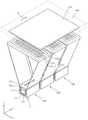
도 1은 본 발명의 일 실시예에 관한 패터닝 슬릿 시트 어셈블리를 개략적으로 도시한 단면도이다.
도 2는 도 1의 A 방향에서 본 평면도이다.
도 3a는 도 1의 프레임과 차폐부를 도시한 사시도이다.
도 3b는 도 3a의 변형예이다.
도 4는 본 발명의 일 실시예에 관한 유기막 증착 장치를 개략적으로 도시한 사시도이다.
도 5는 도 4의 유기막 증착 장치의 개략적인 측단면도이다.
도 6은 도 4의 유기막 증착 장치의 개략적인 평단면도이다.
도 7은 본 발명의 다른 실시예에 관한 유기막 증착 장치를 개략적으로 도시한 사시도이다.
도 8은 본 발명의 또 다른 실시예에 관한 유기막 증착 장치를 개략적으로 도시한 사시도이다.
도 9는 본 발명의 또 다른 실시예에 관한 유기막 증착 장치를 개략적으로 도시한 사시도이다.
도 10은 도 9의 유기막 증착 장치의 개략적인 측단면도이다.
도 11은 도 9의 유기막 증착 장치의 개략적인 평단면도이다.
도 12는 본 발명의 또 다른 실시예에 관한 유기막 증착 장치를 개략적으로 도시한 사시도이다.
도 13은 본 발명에 따른 유기막 증착 장치를 이용하여 제조한 유기 발광 표시 장치를 개략적으로 도시한 단면도이다.1 is a cross-sectional view schematically showing a patterning slit sheet assembly according to an embodiment of the present invention.
2 is a plan view viewed from direction A of Fig.
FIG. 3A is a perspective view showing the frame and the shielding portion of FIG. 1. FIG.
FIG. 3B is a modification of FIG. 3A.
4 is a perspective view schematically showing an organic film deposition apparatus according to an embodiment of the present invention.
5 is a schematic side cross-sectional view of the organic film deposition apparatus of FIG.
6 is a schematic plan sectional view of the organic film deposition apparatus of FIG.
7 is a perspective view schematically showing an organic film deposition apparatus according to another embodiment of the present invention.
8 is a perspective view schematically showing an organic film deposition apparatus according to another embodiment of the present invention.
9 is a perspective view schematically showing an organic film deposition apparatus according to another embodiment of the present invention.
10 is a schematic side cross-sectional view of the organic film deposition apparatus of FIG.
11 is a schematic plan sectional view of the organic film deposition apparatus of FIG.
12 is a perspective view schematically showing an organic film deposition apparatus according to another embodiment of the present invention.
FIG. 13 is a cross-sectional view schematically showing an organic light emitting display device manufactured using the organic film deposition apparatus according to the present invention.
이하 첨부된 도면들에 도시된 본 발명에 관한 실시예를 참조하여 본 발명의 구성 및 작용을 상세히 설명한다.DETAILED DESCRIPTION OF THE PREFERRED EMBODIMENTS Hereinafter, the present invention will be described in detail with reference to the accompanying drawings.
도 1은 본 발명의 일 실시예에 관한 패터닝 슬릿 시트 어셈블리를 개략적으로 도시한 단면도이고, 도 2는 도 1의 A 방향에서 본 평면도이고, 도 3a는 도 1의 프레임과 차폐부를 도시한 사시도이고, 도 3b는 도 3a의 변형예이다.FIG. 1 is a cross-sectional view schematically showing a patterning slit sheet assembly according to an embodiment of the present invention, FIG. 2 is a plan view seen from direction A in FIG. 1, FIG. 3a is a perspective view showing a frame and a shielding portion in FIG. 1 And Fig. 3B is a modification of Fig. 3A.
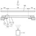
도 1을 참조하면 패터닝 슬릿 시트 어셈블리(150)는 패터닝 슬릿 시트(151), 프레임(154) 및 차폐부(155)를 포함한다.Referring to FIG. 1, the patterning
구체적으로 도 1에는 패터닝 슬릿 시트 어셈블리(150)를 이용하여 기판(500)에 증착 공정을 진행하는 것을 도시하고 있다. 패터닝 슬릿 시트 어셈블리(150)의 하부에는 증착원(110)이 배치되고, 패터닝 슬릿 시트 어셈블리(150)의 상부에는 기판(500)이 배치된다.More specifically, FIG. 1 illustrates the deposition process on the
패터닝 슬릿 시트(151)는 슬릿부(152) 및 무공부(153)를 포함한다. 슬릿부(152)는 소정의 패턴으로 형성된 복수 개의 슬릿(미도시)들을 구비한다. 설명의 편의를 위하여 도 1 및 도 2의 슬릿부(152)에 복수 개의 슬릿을 구체적으로 도시하지는 않았다.The
증착원(110)의 증착 물질은 슬릿부(152)에 구비된 슬릿들을 통하여 진행하여 기판(500)에 증착된다.The deposition material of the
무공부(153)는 슬릿이 형성되지 않은 영역이다. 패터닝 슬릿 시트(151)는 다양한 방법을 이용하여 형성할 수 있는데, 예를 들면 금속 박막을 선택적으로 에칭하여 복수의 슬릿들을 형성하여 슬릿부(152)를 형성하고, 결과적으로 에칭이 되지 않은 영역은 무공부(153)가 된다.The non-coating 153 is an area where no slit is formed. The
패터닝 슬릿 시트(151)는 프레임(154)에 결합된다. 프레임(154)은 대략적으로 창문 틀과 같은 격자 형태로 형성된다. 프레임(154)은 패터닝 슬릿 시트(151)의 무공부(153)의 일 면과 접합되는데 이 때 프레임(154)이 패터닝 슬릿 시트(151)에 소정의 인장력을 부여할 수 있도록 프레임(154)과 패터닝 슬릿 시트(151)가 결합되도록 한다.The
상세히, 패터닝 슬릿 시트(151)의 정밀도는 패터닝 슬릿 시트(151)의 제작 오차와, 증착 공정 진행중 패터닝 슬릿 시트(151)의 열팽창에 의한 오차로 나눌 수 있다. 여기서, 패터닝 슬릿 시트(151)의 제작 오차를 최소화하기 위해, 카운터 포스(Counter Force) 기술을 적용할 수 있다. 이를 더욱 상세히 설명하면 다음과 같다. 먼저, 패터닝 슬릿 시트(151)를 내측에서 외측으로 가압하여 패터닝 슬릿 시트(151)를 인장시킨다. 다음으로, 패터닝 슬릿 시트(151)에 가하여지는 가압력과 대응되는 방향, 즉 반대 방향으로 프레임(154)에 압축력을 가하여, 패터닝 슬릿 시트(151)에 가하여지는 외력과 평형을 이루도록 한다. 다음으로, 프레임(154)과 패터닝 슬릿 시트(151)를 용접 등의 방법으로 결합한다. 마지막으로, 패터닝 슬릿 시트(151)와 프레임(154)에 평형을 이루도록 작용하는 외력을 제거하면, 프레임(154)에 의해 패터닝 슬릿 시트(151)에 인장력이 가하여지게 된다. 이와 같은 정밀 인장/압축/용접 기술을 이용하면, 에칭 산포가 있더라도 패터닝 슬릿 시트(151) 제작 오차는 2um 이하로 제작이 가능하다.In detail, the accuracy of the
한편 증착 공정 중 패터닝 슬릿 시트(151)의 변형, 특히 아래로 처지는 현상을 방지하기 위해서는 소정의 비율 이상으로 인장되도록 소정의 크기 이상의 인장력이 가해지는 것이 필요하다. 즉 프레임(154)에 소정의 크기 이상의 압축력이 가해져야 한다. 그러나 프레임(154)의 변형의 우려가 있어 프레임(154)에 소정의 크기 이상의 압축력을 가하는 경우 문제가 되고, 특히 대형의 기판(500)에 증착 공정을 진행하기 위하여 패터닝 슬릿 시트(151)가 대형화하는 경우 패터닝 슬릿 시트(151)에 가해져야 하는 인장력은 커지고, 그에 대응하는 프레임(154)에 가해지는 압축력도 커진다. 결과적으로 이러한 압축력에 의하여 프레임(154)이 휘어지게 될 수 있고, 프레임(154)의 휘어짐을 방지하기 위하여 프레임(154)의 무게를 급격하게 늘리게 되어 공정 적용이 힘들다.On the other hand, in order to prevent the deformation of the
그러나 본 실시예에서는 패터닝 슬릿 시트(151)의 슬릿부(152)를 증착이 진행될 영역보다 크게 형성한다.However, in this embodiment, the
구체적으로 설명하기로 한다. 도 1에 도시된 대로 기판(500)의 비증착 영역(NA)들 사이에 증착 영역(DA)이 구비되는데, 증착원(110)의 증착 물질은 패터닝 슬릿 시트(151)를 통과하여 기판(500)의 증착 영역(DA)에 도달하여 증착 공정이 진행된다.This will be described in detail. 1, a deposition area DA is provided between the non-deposition areas NA of the
이 때 슬릿부(152)를 증착 영역(DA)과 중첩되고, 증착 영역(DA)보다 크게 형성한다. 즉 슬릿부(152)가 비증착 영역(NA)에까지 이르도록 한다.At this time, the
이를 통하여 무공부(153)의 영역이 줄어들고 슬릿(미도시)들이 구비된 슬릿부(152)의 영역이 늘어나게 된다. 동일한 크기의 인장력을 가하였을 때 슬릿부(152)의 크기가 늘어날수록 관통부 형태의 슬릿(미도시)들로 인하여 패터닝 슬릿 시트(151)가 인장되는 양이 커진다. 즉 동일한 크기의 인장력을 가해도 슬릿부(152)의 크기가 큰 경우에 패터닝 슬릿 시트(151)의 인장되는 양이 크다.As a result, the area of the
그러므로 슬릿부(152)를 크게 할수록 패터닝 슬릿 시트(151)에 가해져야 할 인장력은 작아진다. 결과적으로 프레임(154)에 가해지는 압축력도 줄어든다. 그러므로 프레임(154)의 변형을 방지하고, 프레임(154)의 두께를 증가할 필요가 없어 공정의 편의성이 증가한다.Therefore, the larger the
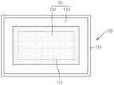
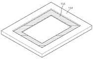
차폐부(155)는 프레임(154)의 내측면에 형성된다. 이 때 차폐부(155)는 도 3a에 도시된 대로 프레임(154)의 내측면을 감싸도록 형성될 수도 있고, 도 3b에 도시된 대로 프레임(154)의 일측면 및 이와 마주보는 일측면에 형성될 수도 있다. 이러한 차폐부(155)의 구성은 공정을 진행할 기판(500), 패터닝 슬릿 시트(151) 및 프레임(154)의 형태, 크기에 따라 다양하게 할 수 있다.The shielding
차폐부(155)는 도 1에 도시된 대로 기판(500)의 비증착 영역(NA)와 중첩되고 증착 영역(DA)의 주변에 대응되도록 형성된다. 전술한 대로 슬릿부(152)가 증착 영역(DA)보다 크게 형성되므로 증착원(110)의 증착 물질이 증착 영역(DA)뿐만 아니라 비증착 영역(NA)에도 증착될 수 있는데 이 경우 원하는 패턴으로 증착이 곤란해진다. 차폐부(155)를 통하여 이러한 것을 방지한다. 즉 차폐부(155)를 통하여 증착원(110)의 증착 물질이 증착이 되어야 하는 증착 영역(DA)에만 증착이 되도록 한다.The
본 실시예의 패터닝 슬릿 시트 어셈블리(150)는 프레임(154)과 패터닝 슬릿 시트(151)를 결합 시 패터닝 슬릿 시트(151)에 인장력이 가해지도록 하여 패터닝 슬릿 시트(151)의 오차를 최소화하고 변형을 방지하여 기판(500)에 원하는 대로 정밀한 패턴으로 증착 공정을 진행할 수 있다.The patterning slit
또한 패터닝 슬릿 시트(151)의 슬릿부(152)를 크게, 구체적으로 증착 영역(DA)보다 크게 형성하여 패터닝 슬릿 시트(151)에 가해지는 인장력을 감소하여 프레임(154)에 가해지는 압축력을 감소하고 결과적으로 프레임(154)의 변형을 방지한다.The
또한 프레임(154)에 차폐부(155)를 형성하여 증착 물질이 비증착 영역(NA)에 증착되지 않고 원하는 대로 증착 영역(DA)에만 증착되도록 하여 정밀 패턴의 증착 공정의 효율성을 증대한다.In addition, a shielding
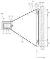
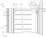
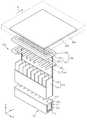
도 4는 본 발명의 일 실시예에 관한 유기막 증착 장치를 개략적으로 도시한 사시도이고, 도 5는 도 4의 유기막 증착 장치의 개략적인 측단면도이고, 도 6은 도 4의 유기막 증착 장치의 개략적인 평단면도이다. 도 4 내지 도 6을 참조하면, 본 발명의 일 실시예에 관한 유기막 증착 장치(100)는 증착원(110), 증착원 노즐부(120), 및 패터닝 슬릿 시트 어셈블리(150)를 포함한다.FIG. 4 is a perspective view schematically showing an organic film deposition apparatus according to an embodiment of the present invention, FIG. 5 is a schematic side cross-sectional view of the organic film deposition apparatus of FIG. 4, Fig. 4 to 6, an organic
상세히, 증착원(110)에서 방출된 증착 물질(115)이 증착원 노즐부(120) 및 패터닝 슬릿 시트 어셈블리(150)를 통과하여 기판(500)에 원하는 패턴으로 증착된다. 도시하지 않았으나 유기막 증착 장치(100)를 통한 증착 공정은 고진공 상태를 유지한 챔버내에서 진행되는 것이 바람직하다. 또한 패터닝 슬릿 시트(151)의 온도가 증착원(110) 온도보다 충분히 낮아야(약 섭씨 100도 이하) 한다. 왜냐하면, 패터닝 슬릿 시트(151)의 온도가 충분히 낮아야만 온도에 의한 패터닝 슬릿 시트(151)의 열팽창 문제를 최소화할 수 있기 때문이다.The
기판(500)은 평판 표시 장치용 기판이 될 수 있는데, 다수의 평판 표시 장치를 형성할 수 있는 마더 글라스(mother glass)와 같은 대면적 기판이 적용될 수 있다. 본 실시예에서는, 기판(500)이 유기막 증착 장치(100)에 대하여 상대적으로 이동하면서 증착이 진행되는 것을 일 특징으로 한다. 기판(500)은 정전척(600)상에 배치된 채 이송될 수 있다.The
상세히, 기존 FMM(fine metal mask) 증착 방법에서는 FMM 크기가 기판 크기와 동일하게 형성되어야 한다. 따라서, 기판 사이즈가 증가할수록 FMM도 대형화되어야 하며, 이로 인해 FMM 제작이 용이하지 않고, FMM을 인장하여 정밀한 패턴으로 얼라인(align) 하기도 용이하지 않다는 문제점이 존재하였다.In detail, in the conventional FMM (fine metal mask) deposition method, the FMM size should be the same as the substrate size. Therefore, as the substrate size increases, the FMM must be made larger, which makes it difficult to fabricate the FMM, and it is not easy to align the FMM with a precise pattern by pulling the FMM.
이와 같은 문제점을 해결하기 위하여, 본 발명의 일 실시예에 관한 유기막 증착 장치(100)는, 유기막 증착 장치(100)와 기판(500)이 서로 상대적으로 이동하면서 증착이 이루어지는 것을 일 특징으로 한다. 다시 말하면, 유기막 증착 장치(100)와 마주보도록 배치된 기판(500)이 Y축 방향을 따라 이동하면서 연속적으로 증착을 수행하게 된다. 즉, 기판(500)이 도 4의 화살표 A 방향(제1 방향)으로 이동하면서 스캐닝(scanning) 방식으로 증착이 수행되는 것이다.In order to solve such problems, the organic
본 발명의 유기막 증착 장치(100)에서는 종래의 FMM에 비하여 훨씬 작게 패터닝 슬릿 시트(151)를 만들 수 있다. 즉, 본 발명의 유기막 증착 장치(100)의 경우, 기판(500)이 Y축 방향을 따라 이동하면서 연속적으로, 즉 스캐닝(scanning) 방식으로 증착을 수행하기 때문에, 패터닝 슬릿 시트(151)의 X축 방향 및 Y축 방향의 길이는 기판(500)의 길이보다 훨씬 작게 형성될 수 있는 것이다. 이와 같이, 종래의 FMM에 비하여 훨씬 작게 패터닝 슬릿 시트(151)를 만들 수 있기 때문에, 본 발명의 패터닝 슬릿 시트(151)는 그 제조가 용이하다. 즉, 패터닝 슬릿 시트(151)의 에칭 작업이나, 그 이후의 정밀 인장 및 용접 작업, 이동 및 세정 작업 등 모든 공정에서, 작은 크기의 패터닝 슬릿 시트(151)가 FMM 증착 방법에 비해 유리하다. 또한, 이는 디스플레이 장치가 대형화될수록 더욱 유리하게 된다.The
한편, 기판(500)과 대향하는 측에는, 증착 물질(115)이 수납 및 가열되는 증착원(110)이 배치된다. 증착원(110) 내에 수납되어 있는 증착 물질(115)이 기화됨에 따라 기판(500)에 증착이 이루어진다.On the other hand, on the side opposite to the
상세히, 증착원(110)은 그 내부에 증착 물질(115)이 채워지는 도가니(112)와, 도가니(112)를 가열시켜 도가니(112) 내부에 채워진 증착 물질(115)을 도가니(112)의 일 측, 상세하게는 증착원 노즐부(120) 측으로 증발시키기 위한 냉각 블록(111)을 포함한다. 냉각 블록(111)은 도가니(112)로부터의 열이 발산되는 것을 최대한 억제하기 위한 것으로, 이 냉각 블록(111)에는 도가니(112)를 가열시키는 히터(미도시)가 포함되어 있다.In detail, the
증착원(110)의 일측, 상세하게는 증착원(110)에서 기판(500)을 향하는 측에는 증착원 노즐부(120)가 배치된다. 그리고, 증착원 노즐부(120)에는, Y축 방향 즉 기판(500)의 스캔 방향을 따라서 복수 개의 증착원 노즐(121)들이 형성된다. 여기서, 상기 복수 개의 증착원 노즐(121)들은 등 간격으로 형성될 수 있다. 증착원(110) 내에서 기화된 증착 물질(115)은 이와 같은 증착원 노즐부(120)를 통과하여 피 증착체인 기판(500) 쪽으로 향하게 되는 것이다. 이와 같이, 증착원 노즐부(120) 상에 Y축 방향 즉 기판(500)의 스캔 방향을 따라서 복수 개의 증착원 노즐(121)들이 형성할 경우, 패터닝 슬릿 시트(151)의 슬릿부(152)를 통과하는 증착 물질에 의해 형성되는 패턴의 크기는 증착원 노즐(121) 하나의 크기에만 영향을 받으므로(즉, X축 방향으로는 증착원 노즐(121)이 하나만 존재하는 것에 다름 아니므로), 음영(shadow)이 발생하지 않게 된다. 또한, 다수 개의 증착원 노즐(121)들이 스캔 방향으로 존재하므로, 개별 증착원 노즐(121) 간 플럭스(flux) 차이가 발생하여도 그 차이가 상쇄되어 증착 균일도가 일정하게 유지되는 효과를 얻을 수 있다.The evaporation
증착원(110)과 기판(500) 사이에는 패터닝 슬릿 시트(151), 프레임(154) 및 차폐부(155)를 구비하는 패터닝 슬릿 시트 어셈블리(150)가 배치된다. 패터닝 슬릿 시트(151)는 슬릿부(152) 및 무공부(153)를 포함하는데, 슬릿부(152)는 X축 방향을 따라서 복수 개의 슬릿들이 형성된다. 증착원(110) 내에서 기화된 증착 물질(115)은 증착원 노즐부(120) 및 패터닝 슬릿 시트(151), 구체적으로 슬릿부(152)를 통과하여 피 증착체인 기판(500) 쪽으로 향하게 되는 것이다.A patterning
패터닝 슬릿 시트(151), 프레임(154) 및 차폐부(155)를 구비하는 패터닝 슬릿 시트 어셈블리(150)의 구성은 전술한 실시예와 동일하므로 구체적인 구성에 대한 설명은 생략하기로 한다.The structure of the patterning
증착원(110) 및 증착원 노즐부(120)와 패터닝 슬릿 시트 어셈블리(150)는 서로 일정 정도 이격되도록 형성될 수 있으며, 증착원(110)(및 이와 결합된 증착원 노즐부(120))과 패터닝 슬릿 시트 어셈블리(150)는 연결 부재(135)에 의하여 서로 연결될 수 있다. 즉, 증착원(110), 증착원 노즐부(120) 및 패터닝 슬릿 시트 어셈블리(150)가 연결 부재(135)에 의해 연결되어 서로 일체로 형성될 수 있는 것이다. 여기서 연결 부재(135)들은 증착원 노즐(121)을 통해 배출되는 증착 물질이 분산되지 않도록 증착 물질의 이동 경로를 가이드 할 수 있다. 도 4에는 연결 부재(135)가 증착원(110), 증착원 노즐부(120) 및 패터닝 슬릿 시트 어셈블리(150)의 좌우 방향으로만 형성되어 증착 물질의 X축 방향만을 가이드 하는 것으로 도시되어 있으나, 이는 도시의 편의를 위한 것으로, 본 발명의 사상은 이에 제한되지 아니하며, 연결 부재(135)가 박스 형태의 밀폐형으로 형성되어 증착 물질의 X축 방향 및 Y축 방향 이동을 동시에 가이드 할 수도 있다.The
상술한 바와 같이, 본 발명의 일 실시예에 관한 유기막 증착 장치(100)는 기판(500)에 대하여 상대적으로 이동하면서 증착을 수행하며, 이와 같이 유기막 증착 장치(100)가 기판(500)에 대하여 상대적으로 이동하기 위해서 패터닝 슬릿 시트 어셈블리(150)는 기판(500)으로부터 일정 정도 이격되도록 형성된다.As described above, the organic
상세히, 종래의 FMM 증착 방법에서는 기판에 음영(shadow)이 생기지 않도록 하기 위하여 기판에 마스크를 밀착시켜서 증착 공정을 진행하였다. 그러나, 이와 같이 기판에 마스크를 밀착시킬 경우, 기판과 마스크 간의 접촉에 의한 불량 문제가 발생한다는 문제점이 존재하였다. 또한, 마스크를 기판에 대하여 이동시킬 수 없기 때문에, 마스크가 기판과 동일한 크기로 형성되어야 한다. 따라서, 디스플레이 장치가 대형화됨에 따라 마스크의 크기도 커져야 하는데, 이와 같은 대형 마스크를 형성하는 것이 용이하지 아니하다는 문제점이 존재하였다.In detail, in the conventional FMM deposition method, a mask is closely adhered to a substrate to prevent a shadow from being formed on the substrate, and a deposition process is performed. However, when the mask is brought into close contact with the substrate in this manner, there is a problem that a problem of defective due to contact between the substrate and the mask occurs. Further, since the mask can not be moved relative to the substrate, the mask must be formed to have the same size as the substrate. Therefore, as the size of the display device is increased, the size of the mask must be increased. Thus, there is a problem that it is not easy to form such a large mask.
그러나 본 실시예의 유기막 증착 장치(100)는 패터닝 슬릿 시트 어셈블리(150)가 피 증착체인 기판(500)과 소정 간격을 두고 이격되도록 배치되도록 한다. 이를 통하여 증착 공정 중 패터닝 슬릿 시트 어셈블리(150)가 기판(500)에 접촉하여 발생하는 불량을 방지한다.However, the organic
또한 패터닝 슬릿 시트 어셈블리(150)의 크기, 특히 패터닝 슬릿 시트(151)의 크기를 기판(500)보다 작게 형성하는 것이 가능하므로 패터닝 슬릿 시트 어셈블리(150)의 제작이 용이해진다.In addition, since the size of the patterning
도 7은 본 발명의 다른 실시예에 관한 유기막 증착 장치를 개략적으로 도시한 사시도이다.7 is a perspective view schematically showing an organic film deposition apparatus according to another embodiment of the present invention.
도 7을 참조하면, 유기막 증착 장치(100)는 증착원(110), 증착원 노즐부(120) 및 패터닝 슬릿 시트 어셈블리(150)를 포함한다.Referring to FIG. 7, the organic
증착원(110)은 그 내부에 증착 물질(115)이 채워지는 도가니(112), 도가니(112)를 가열시켜 도가니(112) 내부에 채워진 증착 물질(115)을 증착원 노즐부(120) 측으로 증발시키기 위한 냉각 블록(111)을 포함한다. 한편, 증착원(110)의 일 측에는 증착원 노즐부(120)가 배치되고, 증착원 노즐부(120)에는 Y축 방향을 따라서 복수 개의 증착원 노즐(121)들이 형성된다. 한편, 증착원(110)과 기판(500) 사이에는 패터닝 슬릿 시트 어셈블리(150)가 구비된다. 그리고, 증착원(110) 및 증착원 노즐부(120)와 패터닝 슬릿 시트 어셈블리(150)는 연결 부재(135)에 의해서 결합된다.The
패터닝 슬릿 시트(151), 프레임(154) 및 차폐부(155)를 구비하는 패터닝 슬릿 시트 어셈블리(150)의 구성은 전술한 실시예와 동일하므로 구체적인 구성에 대한 설명은 생략하기로 한다.The structure of the patterning
본 실시예에서는, 증착원 노즐부(120)에 형성된 복수 개의 증착원 노즐(121)들이 소정 각도 틸트(tilt)되어 배치된다는 점에서 도 4와 구별된다. 상세히, 증착원 노즐(121)은 두 열의 증착원 노즐(121a)(121b)들로 이루어질 수 있으며, 두 열의 증착원 노즐(121a)(121b)들은 서로 교번하여 배치된다. 이때, 증착원 노즐(121a)(121b)들은 XZ 평면상에서 소정 각도 기울어지도록 틸트(tilt)되어 형성될 수 있다.This embodiment is different from FIG. 4 in that a plurality of evaporation source nozzles 121 formed in the evaporation
본 실시예에서는 증착원 노즐(121a)(121b)들이 소정 각도 틸트되어 배치되도록 한다. 여기서, 제1 열의 증착원 노즐(121a)들은 제2 열의 증착원 노즐(121b)들을 바라보도록 틸트되고, 제2 열의 증착원 노즐(121b)들은 제1 열의 증착원 노즐(121a)들을 바라보도록 틸트될 수 있다. 다시 말하면, 왼쪽 열에 배치된 증착원 노즐(121a)들은 패터닝 슬릿 시트 어셈블리(150)의 오른쪽 단부를 바라보도록 배치되고, 오른쪽 열에 배치된 증착원 노즐(121b)들은 패터닝 슬릿 시트 어셈블리(150)의 왼쪽 단부를 바라보도록 배치될 수 있는 것이다.In this embodiment, the
이와 같은 구성에 의하여, 기판(500)의 중앙과 끝 부분에서의 성막 두께 차이가 감소하게 되어 전체적인 증착 물질의 두께가 균일하도록 증착량을 제어할 수 있으며, 나아가서는 재료 이용 효율이 증가하는 효과를 얻을 수 있다.With such a structure, the difference in film thickness between the center and the end of the
도 8은 본 발명의 또 다른 실시예에 관한 유기막 증착 장치를 개략적으로 도시한 사시도이다.8 is a perspective view schematically showing an organic film deposition apparatus according to another embodiment of the present invention.
도 8을 참조하면, 유기막 증착 장치는 도 4 내지 도 6에서 설명한 유기막 증착 장치가 복수 개 구비되는 것을 일 특징으로 한다. 다시 말하면, 본 발명의 일 실시예에 관한 유기막 증착 장치는, 적색 발광층(R) 재료, 녹색 발광층(G) 재료, 청색 발광층(B) 재료가 한꺼번에 방사되는 멀티 증착원(multi source)을 구비할 수 있는 것이다.Referring to FIG. 8, the organic film deposition apparatus has a plurality of organic film deposition apparatuses as shown in FIGS. 4 to 6. In other words, the organic film deposition apparatus according to one embodiment of the present invention includes a multi source in which a red light emitting layer (R) material, a green light emitting layer (G) material, and a blue light emitting layer (B) You can do it.
상세히, 본 실시예는 제1 유기막 증착 장치(100), 제2 유기막 증착 장치(200) 및 제3 유기막 증착 장치(300)를 포함한다. 이와 같은 제1 유기막 증착 장치(100), 제2 유기막 증착 장치(200) 및 제3 유기막 증착 장치(300) 각각의 구성은 도 4 내지 도 6에서 설명한 유기막 증착 장치와 동일하므로 여기서는 그 상세한 설명은 생략하도록 한다.Specifically, this embodiment includes a first organic
또한 패터닝 슬릿 시트(151), 프레임(154) 및 차폐부(155)를 구비하는 패터닝 슬릿 시트 어셈블리(150)의 구성도 전술한 실시예와 동일하므로 구체적인 구성에 대한 설명은 생략하기로 한다.The structure of the patterning
제1 유기막 증착 장치(100), 제2 유기막 증착 장치(200) 및 제3 유기막 증착 장치(300)의 증착원에는 서로 다른 증착 물질들이 구비될 수 있다. 예를 들어, 제1 유기막 증착 장치(100)에는 적색 발광층(R)의 재료가 되는 증착 물질이 구비되고, 제2 유기막 증착 장치(200)에는 녹색 발광층(G)의 재료가 되는 증착 물질이 구비되고, 제3 유기막 증착 장치(300)에는 청색 발광층(B)의 재료가 되는 증착 물질이 구비될 수 있다.The deposition sources of the first organic
본 실시예에 관한 유기막 증착 장치를 이용하면, 하나의 멀티 소스로 적색 발광층(R), 녹색 발광층(G) 및 청색 발광층(B)을 한꺼번에 증착할 수 있다. 따라서, 유기 발광 표시 장치의 생산 시간이 획기적으로 감소하는 동시에, 구비되어야 하는 챔버 수가 감소함으로써, 설비 비용 또한 현저하게 절감되는 효과를 얻을 수 있다.When the organic film deposition apparatus according to the present embodiment is used, the red light-emitting layer (R), the green light-emitting layer (G), and the blue light-emitting layer (B) can be simultaneously deposited with one multi-source. Therefore, the production time of the organic light emitting display device is drastically reduced, and the number of chambers to be provided is reduced, so that the facility cost is remarkably reduced.
도 8에는 자세히 도시되지 않았지만, 제1 유기막 증착 장치(100), 제2 유기막 증착 장치(200) 및 제3 유기막 증착 장치(300)의 패터닝 슬릿 시트 어셈블리(150)들은 서로 일정 정도 오프셋(offset)되어 배치됨으로써, 그 증착 영역이 중첩되지 아니하도록 할 수 있다. 다시 말하면, 제1 유기막 증착 장치(100)가 적색 발광층(R)의 증착을 담당하고, 제2 유기막 증착 장치(200)가 녹색 발광층(G)의 증착을 담당하고, 제3 유기막 증착 장치(300)가 청색 발광층(B)의 증착을 담당할 경우, 제1 유기막 증착 장치(100)의 패터닝 슬릿 시트(151)의 슬릿부(152)에 구비된 슬릿과 제2 유기막 증착 장치(200)의 패터닝 슬릿 시트(151)의 슬릿부(152)에 구비된 슬릿과 제3 유기막 증착 장치(300)의 패터닝 슬릿 시트(151)의 슬릿부(152)에 구비된 슬릿이 서로 동일 선상에 위치하지 아니하도록 배치됨으로써, 기판상의 서로 다른 영역에 각각 적색 발광층(R), 녹색 발광층(G), 청색 발광층(B)이 형성되도록 할 수 있다.8, the patterning
여기서, 적색 발광층(R)의 재료가 되는 증착 물질과, 녹색 발광층(G)의 재료가 되는 증착 물질과, 청색 발광층(B)의 재료가 되는 증착 물질은 서로 기화되는 온도가 상이할 수 있으므로, 상기 제1 유기막 증착 장치(100)의 증착원(110)의 온도와 상기 제2 유기막 증착 장치(200)의 증착원의 온도와 상기 제3 유기막 증착 장치(300)의 증착원의 온도가 서로 다르도록 설정되는 것도 가능하다 할 것이다.Here, the deposition material to be the material of the red luminescent layer (R), the deposition material to be the material of the green luminescent layer (G), and the deposition material to be the material of the blue luminescent layer (B) The temperature of the
한편, 도면에는 유기막 증착 장치가 세 개 구비되는 것으로 도시되어 있으나, 본 발명의 사상은 이에 제한되지 아니한다. 즉, 본 실시예에 관한 유기막 증착 장치는 유기막 증착 장치를 다수 개 구비할 수 있으며, 상기 다수 개의 유기막 증착 장치 각각에 서로 다른 물질들을 구비할 수 있다. 예를 들어, 유기막 증착 장치를 다섯 개 구비하여, 각각의 유기막 증착 장치에 적색 발광층(R), 녹색 발광층(G), 청색 발광층(B) 및 적색 발광층의 보조층(R')과 녹색 발광층의 보조층(G')을 구비할 수 있다.In the meantime, although three organic film deposition apparatuses are shown in the figure, the present invention is not limited thereto. That is, the organic film deposition apparatus according to the present embodiment may include a plurality of organic film deposition apparatuses, and each of the plurality of organic film deposition apparatuses may have different materials. For example, five organic film deposition apparatuses are provided, and a red light emitting layer (R), a green light emitting layer (G), a blue light emitting layer (B), an auxiliary layer (R ' And an auxiliary layer G 'of the light emitting layer.
복수 개의 유기막 증착 장치를 구비하여, 다수 개의 박막층을 한번에 형성할 수 있도록 함으로써, 제조 수율 및 증착 효율이 향상되는 효과를 얻을 수 있다. 또한, 제조 공정이 간단해지고 제조 비용이 감소하는 효과를 얻을 수 있다.By providing a plurality of organic film deposition apparatuses so that a plurality of thin film layers can be formed all at once, an effect of improving the production yield and deposition efficiency can be obtained. Further, the manufacturing process can be simplified and the manufacturing cost can be reduced.
도 9는 본 발명의 또 다른 실시예에 관한 유기막 증착 장치를 개략적으로 도시한 사시도이고, 도 10은 도 9의 유기막 증착 장치의 개략적인 측단면도이고, 도 11은 도 9의 유기막 증착 장치의 개략적인 평단면도이다.FIG. 9 is a perspective view schematically showing an organic film deposition apparatus according to another embodiment of the present invention, FIG. 10 is a schematic side sectional view of the organic film deposition apparatus of FIG. 9, and FIG. 11 is a cross- 1 is a schematic plan sectional view of the device.
도 9 내지 도 11을 참조하면, 본 발명의 또 다른 실시예에 관한 유기막 증착 장치(100)는 증착원(110), 증착원 노즐부(120), 패터닝 슬릿 시트 어셈블리(150) 및 차단판 어셈블리(130)를 포함한다. 도 9 내지 도 11에는 설명의 편의를 위해 챔버를 도시하지 않았지만, 도 9 내지 도 11의 모든 구성은 적절한 진공도가 유지되는 챔버 내에 배치되는 것이 바람직하다. 이는 증착 물질의 직진성을 확보하기 위함이다.9 to 11, an organic
이러한 챔버 내에는 피 증착체인 기판(500)이 정전척(600)에 의해 이송된다. 상기 기판(500)은 평판 표시 장치용 기판이 될 수 있는 데, 다수의 평판 표시 장치를 형성할 수 있는 마더 글라스(mother glass)와 같은 대면적 기판이 적용될 수 있다.In this chamber, the
본 실시예에서는 기판(500)이 유기막 증착 장치(100)에 대하여 상대적으로 이동하는 데, 바람직하게는 유기막 증착 장치(100)에 대하여 기판(500)이 A방향으로 이동하도록 할 수 있다.In this embodiment, the
전술한 실시예와 같이 본 실시예의 유기막 증착 장치(100)에서는 종래의 FMM에 비하여 훨씬 작게 패터닝 슬릿 시트 어셈블리(150)를 만들 수 있다. 즉, 본 발명의 유기막 증착 장치(100)의 경우, 기판(500)이 Y축 방향을 따라 이동하면서 연속적으로, 즉 스캐닝(scanning) 방식으로 증착을 수행하기 때문에, 패터닝 슬릿 시트(151)의 X축 방향으로의 폭과 기판(500)의 X축 방향으로의 폭만 실질적으로 동일하게 형성되면, 패터닝 슬릿 시트(151)의 Y축 방향의 길이는 기판(500)의 길이보다 훨씬 작게 형성되어도 무방하게 된다. 물론, 패터닝 슬릿 시트(151)의 X축 방향으로의 폭이 기판(500)의 X축 방향으로의 폭보다 작게 형성되더라도, 기판(500)과 유기막 증착 장치(100)의 상대적 이동에 의한 스캐닝 방식에 의해 충분히 기판(500) 전체에 대하여 증착을 할 수 있게 된다.The patterning slit
이와 같이, 종래의 FMM에 비하여 훨씬 작게 패터닝 슬릿 시트(151)를 만들 수 있기 때문에, 본 발명의 패터닝 슬릿 시트(151)는 그 제조가 용이하다.As described above, since the
한편, 기판(500)과 대향하는 측에는, 증착 물질(115)이 수납 및 가열되는 증착원(110)이 배치된다. 증착원(110)은 그 내부에 증착 물질(115)이 채워지는 도가니(112)와, 이 도가니(112)를 둘러싸는 냉각 블록(111)이 구비된다. 냉각 블록(111)은 도가니(112)로부터의 열이 발산되는 것을 최대한 억제하기 위한 것으로, 이 냉각 블록(111)에는 도가니(112)를 가열시키는 히터(미도시)가 포함되어 있다.On the other hand, on the side opposite to the
증착원(110)의 일 측, 상세하게는 증착원(110)에서 기판(500)을 향하는 측에는 증착원 노즐부(120)가 배치된다. 그리고, 증착원 노즐부(120)에는, X축 방향을 따라서 복수 개의 증착원 노즐(121)들이 형성된다. 여기서, 상기 복수 개의 증착원 노즐(121)들은 등 간격으로 형성될 수 있다. 증착원(110) 내에서 기화된 증착 물질(115)은 이와 같은 증착원 노즐부(120)의 증착원 노즐(121)들을 통과하여 피 증착체인 기판(500) 쪽으로 향하게 되는 것이다.The evaporation
증착원 노즐부(120)의 일 측에는 차단판 어셈블리(130)가 구비된다. 차단판 어셈블리(130)는 복수 개의 차단판(131)들과, 차단판(131)들 외측에 구비되는 차단판 프레임(132)을 포함한다. 복수 개의 차단판(131)들은 X축 방향을 따라서 서로 나란하게 배치될 수 있다. 여기서, 복수 개의 차단판(131)들은 등 간격으로 형성될 수 있다. 또한, 각각의 차단판(131)들은 도면에서 보았을 때 YZ평면을 따라 연장되어 있고, 바람직하게는 직사각형으로 구비될 수 있다. 이와 같이 배치된 복수 개의 차단판(131)들은 증착원 노즐부(120)와 패터닝 슬릿 시트 어셈블리(150) 사이의 공간을 복수 개의 증착 공간(S)으로 구획한다. 즉, 본 실시예에 관한 유기막 증착 장치(100)는 차단판(131)들에 의하여, 도 11에서 볼 수 있듯이, 증착 물질이 분사되는 각각의 증착원 노즐(121) 별로 증착 공간(S)이 분리된다.A blocking
여기서, 각각의 차단판(131)들은 서로 이웃하고 있는 증착원 노즐(121)들 사이에 배치될 수 있다. 이는 다시 말하면, 서로 이웃하고 있는 차단판(131)들 사이에 하나의 증착원 노즐(121)이 배치되는 것이다. 바람직하게, 증착원 노즐(121)은 서로 이웃하고 있는 차단판(131) 사이의 정 중앙에 위치할 수 있다. 그러나 본 발명은 반드시 이에 한정되지 않으며, 서로 이웃하고 있는 차단판(131)들 사이에 복수의 증착원 노즐(121)이 배치하여도 무방하다. 다만, 이 경우에도 복수의 증착원 노즐(121)들이 서로 이웃하고 있는 차단판(131) 사이의 정 중앙에 위치하도록 하는 것이 바람직하다.Here, each of the blocking
이와 같이, 차단판(131)이 증착원 노즐부(120)와 패터닝 슬릿 시트 어셈블리(150) 사이의 공간을 복수 개의 증착 공간(S)으로 구획함으로써, 하나의 증착원 노즐(121)로부터 배출되는 증착 물질은 다른 증착원 노즐(121)로부터 배출된 증착 물질들과 혼합되지 않고, 패터닝 슬릿 시트 어셈블리(150)의 슬릿부(152)를 통과하여 기판(500)에 증착되는 것이다. 즉, 차단판(131)들은 각 증착원 노즐(121)을 통해 배출되는 증착 물질이 분산되지 않고 직진성을 유지하도록 증착 물질의 Z축 방향의 이동 경로를 가이드 하는 역할을 수행한다.The blocking
이와 같이, 차단판(131)들을 구비하여 증착 물질의 직진성을 확보함으로써, 기판에 형성되는 음영(shadow)의 크기를 대폭적으로 줄일 수 있으며, 따라서 유기막 증착 장치(100)와 기판(500)을 일정 정도 이격시키는 것이 가능해진다. 이에 대하여는 뒤에서 상세히 기술하기로 한다.Since the
한편, 복수 개의 차단판(131)들의 외측으로는 차단판 프레임(132)이 더 구비될 수 있다. 차단판 프레임(132)은, 복수 개의 차단판(131)들의 측면에 각각 구비되어, 복수 개의 차단판(131)들의 위치를 고정하는 동시에, 증착원 노즐(121)을 통해 배출되는 증착 물질이 Y축 방향으로 분산되지 않도록 한다.Meanwhile, the blocking
증착원 노즐부(120)와 차단판 어셈블리(130)는 일정 정도 이격된 것이 바람직하다. 이에 따라, 증착원(110)으로부터 발산되는 열이 차단판 어셈블리(130)에 전도되는 것을 방지할 수 있다. 그러나, 본 발명의 사상은 이에 제한되지 아니한다. 즉, 증착원 노즐부(120)와 차단판 어셈블리(130) 사이에 적절한 단열 수단이 구비될 경우 증착원 노즐부(120)와 차단판 어셈블리(130)가 결합하여 접촉할 수도 있을 것이다.It is preferable that the evaporation
한편, 차단판 어셈블리(130)는 유기막 증착 장치(100)로부터 착탈 가능하도록 형성될 수 있다. 본 실시예에 관한 유기막 증착 장치(100)에서는 차단판 어셈블리(130)를 이용하여 증착 공간을 외부 공간과 분리하였기 때문에, 기판(500)에 증착되지 않은 증착 물질은 대부분 차단판 어셈블리(130) 내에 증착된다. 따라서, 차단판 어셈블리(130)를 유기막 증착 장치(100)로부터 착탈가능하도록 형성하여, 장시간 증착 후 차단판 어셈블리(130)에 증착 물질이 많이 쌓이게 되면, 차단판 어셈블리(130)를 유기막 증착 장치(100)로부터 분리하여 별도의 증착 물질 재활용 장치에 넣어서 증착 물질을 회수할 수 있다. 이와 같은 구성을 통하여, 증착 물질 재활용률을 높임으로써 증착 효율이 향상되고 제조 비용이 절감되는 효과를 얻을 수 있다.Meanwhile, the blocking
증착원(110)과 기판(500) 사이에는 패터닝 슬릿 시트 어셈블리(150)가 배치된다. 프레임(154)은 대략 창문 틀과 같은 형태로 형성되며, 패터닝 슬릿 시트(151)와 결합된다. 그리고, 패터닝 슬릿 시트(151)는 슬릿부(152) 및 무공부(153)를 구비하고, 슬릿부(152)는 X축 방향을 따라서 복수 개의 슬릿들이 형성된다. 슬릿부(152)의 각 슬릿들은 Y축 방향을 따라 연장되어 있다.A patterning
패터닝 슬릿 시트(151), 프레임(154) 및 차폐부(155)를 구비하는 패터닝 슬릿 시트 어셈블리(150)의 구성은 전술한 실시예와 동일하므로 구체적인 구성에 대한 설명은 생략하기로 한다.The structure of the patterning
여기서, 본 실시예에 관한 유기막 증착 장치(100)는 증착원 노즐(121)들의 총 개수보다 슬릿부(152)에 구비된 슬릿들의 총 개수가 더 많게 형성된다. 또한, 서로 이웃하고 있는 두 개의 차단판(131) 사이에 배치된 증착원 노즐(121)의 개수보다 슬릿부(152)에 구비된 슬릿들의 개수가 더 많게 형성된다. 슬릿부(152)에 구비된 슬릿의 개수는 기판(500)에 형성될 증착 패턴의 개수에 대응되도록 하는 것이 바람직하다.Here, the organic
한편, 상술한 차단판 어셈블리(130)와 패터닝 슬릿 시트 어셈블리(150)는 서로 일정 정도 이격되도록 형성될 수 있으며, 차단판 어셈블리(130)와 패터닝 슬릿 시트 어셈블리(150)는 연결 부재(133)에 의하여 서로 연결될 수 있다.The blocking
상세히, 고온 상태의 증착원(110)에 의해 차단판 어셈블리(130)의 온도는 최대 섭씨 100도 이상 상승하기 때문에, 상승된 차단판 어셈블리(130)의 온도가 패터닝 슬릿 시트 어셈블리(150)로 전도되지 않도록 차단판 어셈블리(130)와 패터닝 슬릿 시트 어셈블리(150)를 일정 정도 이격시키는 것이다.In detail, since the temperature of the
상술한 바와 같이, 본 실시예에 관한 유기막 증착 장치(100)는 기판(500)에 대하여 상대적으로 이동하면서 증착을 수행하며, 이와 같이 유기막 증착 장치(100)가 기판(500)에 대하여 상대적으로 이동하기 위해서 패터닝 슬릿 시트 어셈블리(150)는 기판(500)으로부터 일정 정도 이격되도록 형성된다. 그리고, 패터닝 슬릿 시트 어셈블리(150), 특히 패터닝 슬릿 시트(151)와 기판(500)을 이격시킬 경우 발생하는 음영(shadow) 문제를 해결하기 위하여, 증착원 노즐부(120)와 패터닝 슬릿 시트 어셈블리(150) 사이에 차단판(131)들을 구비하여 증착 물질의 직진성을 확보함으로써, 기판(500)에 형성되는 음영(shadow)의 크기를 대폭적으로 감소시킨 것이다.As described above, the organic
본 실시예의 유기막 증착 장치(100)는 패터닝 슬릿 시트 어셈블리(150)가 피 증착체인 기판(500)과 소정 간격을 두고 이격되도록 배치되도록 한다. 이를 통하여 증착 공정 중 패터닝 슬릿 시트 어셈블리(150)가 기판(500)에 접촉하여 발생하는 불량을 방지한다.The organic
또한 패터닝 슬릿 시트 어셈블리(150)의 크기, 특히 패터닝 슬릿 시트(151)의 크기를 기판(500)보다 작게 형성하는 것이 가능하므로 패터닝 슬릿 시트 어셈블리(150)의 제작이 용이해진다.In addition, since the size of the patterning
도 12는 본 발명의 또 다른 실시예에 관한 유기막 증착 장치를 개략적으로 도시한 사시도이다.12 is a perspective view schematically showing an organic film deposition apparatus according to another embodiment of the present invention.
도 12를 참조하면 유기막 증착 장치(100)는 증착원(110), 증착원 노즐부(120), 제1 차단판 어셈블리(130), 제2 차단판 어셈블리(140) 및 패터닝 슬릿 시트 어셈블리(150)를 포함한다. 도 12에는 설명의 편의를 위해 챔버를 도시하지 않았지만, 도 12의 모든 구성은 적절한 진공도가 유지되는 챔버 내에 배치되는 것이 바람직하다. 이는 증착 물질의 직진성을 확보하기 위함이다.12, the organic
이러한 챔버(미도시) 내에는 피 증착체인 기판(500)이 배치된다. 그리고, 챔버(미도시) 내에서 기판(500)과 대향하는 측에는, 증착 물질(115)이 수납 및 가열되는 증착원(110)이 배치된다. 증착원(110)의 상세한 구성은 전술한 도 11에 따른 실시예와 동일하므로 상세한 설명은 생략한다. 그리고 제1 차단판 어셈블리(130)는 도 11에 따른 실시예의 차단판 어셈블리(130)와 동일하므로 역시 상세한 설명은 생략한다.In this chamber (not shown), a
또한 패터닝 슬릿 시트(151), 프레임(154) 및 차폐부(155)를 구비하는 패터닝 슬릿 시트 어셈블리(150)의 구성도 전술한 실시예와 동일하므로 구체적인 구성에 대한 설명은 생략하기로 한다.The structure of the patterning
본 실시예에서는 제1 차단판 어셈블리(130)의 일 측에 제2 차단판 어셈블리(140)가 배치된다. 제2 차단판 어셈블리(140)는 복수 개의 제2 차단판(141)들과, 제2 차단판(141)들 외측에 구비되는 제2 차단판 프레임(142)을 포함한다.In this embodiment, the second blocking plate assembly 140 is disposed on one side of the first
복수 개의 제2 차단판(141)들은 X축 방향을 따라서 서로 나란하게 구비될 수 있다. 그리고, 복수 개의 제2 차단판(141)들은 등 간격으로 형성될 수 있다. 또한, 각각의 제2 차단판(141)은 도면에서 보았을 때 YZ평면과 나란하도록, 다시 말하면 X축 방향에 수직이 되도록 형성된다.The plurality of second blocking plates 141 may be provided in parallel with each other along the X-axis direction. The plurality of second blocking plates 141 may be formed at regular intervals. Each second blocking plate 141 is formed so as to be parallel to the YZ plane as viewed in the drawing, that is, perpendicular to the X axis direction.
이와 같이 배치된 복수 개의 제1 차단판(131) 및 제2 차단판(141)들은 증착원 노즐부(120)와 패터닝 슬릿 시트 어셈블리(150) 사이의 공간을 구획하는 역할을 수행한다. 즉, 제1 차단판(131) 및 제2 차단판(141)에 의하여, 증착 물질이 분사되는 각각의 증착원 노즐(121) 별로 증착 공간이 분리되는 것을 일 특징으로 한다.The plurality of
여기서, 각각의 제2 차단판(141)들은 각각의 제1 차단판(131)들과 일대일 대응하도록 배치될 수 있다. 다시 말하면, 각각의 제2 차단판(141)들은 각각의 제1 차단판(131)들과 얼라인(align) 되어 서로 나란하게 배치될 수 있다. 즉, 서로 대응하는 제1 차단판(131)과 제2 차단판(141)은 서로 동일한 평면상에 위치하게 되는 것이다. 도면에는, 제1 차단판(131)의 길이와 제2 차단판(141)의 X축 방향의 폭이 동일한 것으로 도시되어 있지만, 본 발명의 사상은 이에 제한되지 아니한다. 즉, 패터닝 슬릿 시트(151)의 슬릿부(152)에 구비된 슬릿들과의 정밀한 얼라인(align)이 요구되는 제2 차단판(141)은 상대적으로 얇게 형성되는 반면, 정밀한 얼라인이 요구되지 않는 제1 차단판(131)은 상대적으로 두껍게 형성되어, 그 제조가 용이하도록 하는 것도 가능하다 할 것이다.Here, each of the second blocking plates 141 may be arranged to correspond one-to-one with the respective
또한 본 실시예의 유기막 증착 장치(100)는 도 8에 도시한 것과 같이 복수개가 연속하여 배치될 수 있다.In addition, a plurality of organic
도 13은 본 발명에 따른 유기막 증착 장치를 이용하여 제조한 유기 발광 표시 장치를 개략적으로 도시한 단면도이다.FIG. 13 is a cross-sectional view schematically showing an organic light emitting display device manufactured using the organic film deposition apparatus according to the present invention.
도 13을 참조하면, 유기 발광 표시 장치는 기판(30) 상에 형성된다. 기판(30)은 투명한 소재, 예컨대 글래스재, 플라스틱재, 또는 금속재로 형성될 수 있다. 기판(30)상에는 전체적으로 절연물을 함유하는 버퍼층(31)이 형성되어 있다.Referring to FIG. 13, an organic light emitting display is formed on a
버퍼층(31)상에는 박막 트랜지스터(40(TFT:thin film transistor))와, 커패시터(50)와, 유기 발광 소자(60)가 형성된다. 박막 트랜지스터(40)는 크게 활성층(41), 게이트 전극(42), 소스/드레인 전극(43)을 포함한다. 유기 발광 소자(60)는 제1 전극(61), 제2 전극(62) 및 중간층(63)을 포함한다.A thin film transistor (TFT) 40, a
구체적으로 버퍼층(31)의 윗면에는 소정 패턴으로 배열된 활성층(41)이 형성되어 있다. 활성층(41)은 p형 또는 n형의 반도체로 구비될 수 있다. 활성층(41)상부에는 게이트 절연막(32)이 형성된다. 게이트 절연막(32)의 상부에는 활성층(41)과 대응되는 곳에 게이트 전극(42)이 형성된다. 게이트 전극(42)을 덮도록 층간 절연막(33)이 형성되고, 층간 절연막(33) 상에 소스/드레인 전극(43)이 형성되는 데, 활성층(41)의 소정의 영역과 접촉되도록 형성된다. 소스/드레인 전극(43)을 덮도록 패시베이션층(34)이 형성되고, 패시베이션층 (34)위로는 패시베이션층 (34)의 평탄화를 위해 별도의 절연막을 더 형성할 수도 있다.Specifically, on the upper surface of the
패시베이션층 (34)상에 제1 전극(61)을 형성한다. 제1 전극(61)은 드레인 전극(43)과 전기적으로 연결되도록 형성한다. 그리고, 제1 전극(61)을 덮도록 화소정의막(35)이 형성된다. 이 화소정의막(35)에 소정의 개구(64)를 형성한 후, 이 개구(64)로 한정된 영역 내에 유기 발광층을 구비하는 중간층(63)을 형성한다. 중간층(63)상에 제 2 전극(62)을 형성한다.A first electrode (61) is formed on the passivation layer (34). The
유기 발광층을 구비하는 중간층(63)은 전술한 실시예의 패터닝 슬릿 시트 어셈블리(150) 및 이를 포함하는 유기막 증착 장치(100)를 이용하여 형성될 수 있다.The
구체적인 예를들면 먼저, 화소 정의막(35)에 개구(64)를 형성한 후, 이 기판(30)을 챔버(미도시)내로 이송한다. 원하는 증착 물질을 이용하여 증착 공정을 진행하여 중간층(63)을 원하는 패턴으로 형성할 수 있다.Specifically, first, an
본 발명은 이 외에도, 유기 TFT의 유기막 또는 무기막 등의 증착에도 사용할 수 있으며, 기타, 다양한 소재의 성막 공정에 적용 가능하다.The present invention can be used for deposition of an organic film or an inorganic film of an organic TFT or the like and can be applied to other various film forming processes.
본 발명은 도면에 도시된 실시예를 참고로 설명되었으나 이는 예시적인 것에 불과하며, 당해 기술 분야에서 통상의 지식을 가진 자라면 이로부터 다양한 변형 및 균등한 다른 실시예가 가능하다는 점을 이해할 것이다. 따라서, 본 발명의 진정한 기술적 보호 범위는 첨부된 특허청구범위의 기술적 사상에 의하여 정해져야 할 것이다.While the present invention has been described with reference to exemplary embodiments, it is to be understood that the invention is not limited to the disclosed exemplary embodiments, but, on the contrary, is intended to cover various modifications and equivalent arrangements included within the spirit and scope of the invention. Accordingly, the true scope of the present invention should be determined by the technical idea of the appended claims.
150: 패터닝 슬릿 시트 어셈블리
151: 패터닝 슬릿 시트
152: 슬릿부
153: 무공부
154: 프레임
155: 차폐부
110: 증착원
500: 기판150: patterning slit sheet assembly
151: patterning slit sheet
152:
153: Non-study
154: frame
155:
110: evaporation source
500: substrate
Claims (26)
Translated fromKorean슬릿부 및 상기 슬릿부의 가장자리에 배치된 무공부를 구비하는 패터닝 슬릿 시트;
상기 패터닝 슬릿 시트를 지지하도록 상기 패터닝 슬릿 시트와 결합되는 프레임 및
상기 프레임의 적어도 하나의 내측면에 형성되고 상기 슬릿부의 영역 중 가장자리를 포함한 소정의 영역과 중첩되는 차폐부를 포함하고,
상기 프레임의 내측면은 제1 측면, 상기 제1 측면과 마주보는 제2 측면, 상기 제1 측면과 제2 측면을 연결하고 서로 마주보도록 형성된 제3 측면 및 제4 측면을 포함하고,
상기 차폐부는 상기 프레임의 내측면 중 제1 측면에 대응되는 제1 영역 및 상기 프레임의 내측면 중 상기 제2 측면에 대응되는 제2 영역을 포함하고,
상기 차폐부의 제1 영역은 상기 프레임의 내측면 중 상기 제3 측면과 상기 제4 측면을 연결하도록 길게 연장된 형태를 갖고,
상기 차폐부의 제2 영역은 상기 프레임의 내측면 중 상기 제3 측면과 상기 제4 측면을 연결하도록 길게 연장된 형태를 갖고,
상기 차폐부의 제1 영역과 제2 영역의 사이에는 이격된 공간이 형성되고 상기 이격된 공간은 상기 슬릿부와 중첩되는 패터닝 슬릿 시트 어셈블리.The present invention relates to a patterning slit sheet assembly for depositing a thin film in a desired pattern on a substrate,
A patterning slit sheet having a slit portion and a non-patterned portion disposed at an edge of the slit portion;
A frame coupled with the patterning slit sheet to support the patterning slit sheet;
And a shielding portion formed on at least one inner surface of the frame and overlapping with a predetermined region including an edge of the region of the slit portion,
Wherein the inner side surface of the frame includes a first side, a second side facing the first side, a third side and a fourth side that are formed to connect the first side and the second side and face each other,
Wherein the shield comprises a first region corresponding to a first side of the inner side of the frame and a second region corresponding to the second side of the inner side of the frame,
The first region of the shield has a shape elongated to connect the third side and the fourth side of the inner side surface of the frame,
The second region of the shield has a shape elongated so as to connect the third side face and the fourth side face among the inner side faces of the frame,
Wherein a spaced space is formed between the first region and the second region of the shield and the spaced space is overlapped with the slit portion.
상기 차폐부는 상기 프레임의 내측면 중 일 측면 및 이와 마주보는 일 측면에 형성되는 패터닝 슬릿 시트 어셈블리.The method according to claim 1,
Wherein the shield is formed on one side of the inner side of the frame and on one side thereof facing the side of the frame.
상기 차폐부는 상기 프레임의 내측면을 감싸도록 형성되는 패터닝 슬릿 시트 어셈블리.The method according to claim 1,
Wherein the shield is configured to enclose an inner surface of the frame.
상기 슬릿부는 상기 기판에 증착되는 영역과 중첩되고 상기 기판에 증착되는 영역보다 크게 형성되는 패터닝 슬릿 시트 어셈블리.The method according to claim 1,
Wherein the slit portion is formed to be larger than an area to be deposited on the substrate and overlap with a region to be deposited on the substrate.
상기 차폐부는 상기 기판에 증착되는 영역의 주변과 대응되도록 형성된 패터닝 슬릿 시트 어셈블리.The method according to claim 1,
Wherein the shield is configured to correspond to a periphery of a region to be deposited on the substrate.
증착 물질을 방사하는 증착원;
상기 증착원의 일 측에 배치되고 제1 방향을 따라 복수 개의 증착원 노즐들이 형성된 증착원 노즐부; 및
슬릿부 및 상기 슬릿부의 가장자리에 배치된 무공부를 구비하는 패터닝 슬릿 시트, 상기 패터닝 슬릿 시트를 지지하도록 상기 패터닝 슬릿 시트와 결합되는 프레임 및 상기 프레임의 적어도 하나의 내측면에 형성되고 상기 슬릿부의 영역 중 가장자리를 포함한 소정의 영역과 중첩되는 차폐부를 구비하는 패터닝 슬릿 시트 어셈블리를 포함하고,
상기 프레임의 내측면은 제1 측면, 상기 제1 측면과 마주보는 제2 측면, 상기 제1 측면과 제2 측면을 연결하고 서로 마주보도록 형성된 제3 측면 및 제4 측면을 포함하고,
상기 차폐부는 상기 프레임의 내측면 중 제1 측면에 대응되는 제1 영역 및 상기 프레임의 내측면 중 상기 제2 측면에 대응되는 제2 영역을 포함하고,
상기 차폐부의 제1 영역은 상기 프레임의 내측면 중 상기 제3 측면과 상기 제4 측면을 연결하도록 길게 연장된 형태를 갖고,
상기 차폐부의 제2 영역은 상기 프레임의 내측면 중 상기 제3 측면과 상기 제4 측면을 연결하도록 길게 연장된 형태를 갖고,
상기 차폐부의 제1 영역과 제2 영역의 사이에는 이격된 공간이 형성되고 상기 이격된 공간은 상기 슬릿부와 중첩되는 유기막 증착 장치.An organic film deposition apparatus for depositing an organic film on a substrate,
An evaporation source for emitting a deposition material;
An evaporation source nozzle unit disposed at one side of the evaporation source and having a plurality of evaporation source nozzles formed along a first direction; And
A patterning slit sheet having a slit portion and an untreated portion disposed at an edge of the slit portion, a frame coupled with the patterning slit sheet to support the patterning slit sheet, and a frame portion formed on at least one inner surface of the frame, And a shielding portion overlapping with a predetermined region including a middle edge of the patterning slit sheet assembly,
Wherein the inner side surface of the frame includes a first side, a second side facing the first side, a third side and a fourth side that are formed to connect the first side and the second side and face each other,
Wherein the shield comprises a first region corresponding to a first side of the inner side of the frame and a second region corresponding to the second side of the inner side of the frame,
The first region of the shield has a shape elongated to connect the third side and the fourth side of the inner side surface of the frame,
The second region of the shield has a shape elongated so as to connect the third side face and the fourth side face among the inner side faces of the frame,
Wherein a space is formed between the first area and the second area of the shield, and the spaced space overlaps the slit part.
상기 차폐부는 상기 프레임의 내측면 중 상기 제1 방향과 수직한 방향을 향하는 양쪽 측면에 형성되는 유기막 증착 장치.The method according to claim 6,
Wherein the shielding portions are formed on both side surfaces of the inner side surface of the frame, the side surfaces being perpendicular to the first direction.
상기 기판이 상기 유기막 증착 장치에 대하여 상기 제1 방향을 따라 이동하면서 증착이 수행되는 유기막 증착 장치.The method according to claim 6,
Wherein the deposition is performed while the substrate moves along the first direction with respect to the organic film deposition apparatus.
상기 증착원, 상기 증착원 노즐부 및 상기 패터닝 슬릿 시트 어셈블리는 일체로 형성되는 유기막 증착 장치.The method according to claim 6,
Wherein the evaporation source, the evaporation source nozzle unit, and the patterning slit sheet assembly are integrally formed.
상기 증착원 및 상기 증착원 노즐부와 상기 패터닝 슬릿 시트 어셈블리는 상기 증착 물질의 이동 경로를 가이드 하는 연결 부재에 의해 결합되어 일체로 형성되는 유기막 증착 장치.The method according to claim 6,
Wherein the evaporation source, the evaporation source nozzle unit, and the patterning slit sheet assembly are integrally formed by a connection member for guiding a movement path of the evaporation material.
상기 연결 부재는 상기 증착원 및 상기 증착원 노즐부와 상기 패터닝 슬릿 시트 어셈블리 사이의 공간을 외부로부터 밀폐하도록 형성되는 유기막 증착 장치.11. The method of claim 10,
Wherein the connecting member is formed to seal the space between the evaporation source and the evaporation source nozzle unit and the patterning slit sheet assembly from the outside.
상기 복수 개의 증착원 노즐들은 소정 각도 틸트 되도록 형성되는 유기막 증착 장치.The method according to claim 6,
Wherein the plurality of evaporation source nozzles are formed to be tilted by a predetermined angle.
상기 복수 개의 증착원 노즐들은 상기 제1 방향을 따라 형성된 두 열(列)의 증착원 노즐들을 포함하며, 상기 두 열(列)의 증착원 노즐들은 서로 마주보는 방향으로 틸트되도록 형성된 유기막 증착 장치.13. The method of claim 12,
Wherein the plurality of evaporation source nozzles include two rows of evaporation source nozzles formed along the first direction and the evaporation source nozzles of the two rows are arranged to be tilted in directions opposite to each other, .
증착 물질을 방사하는 증착원;
상기 증착원의 일 측에 배치되고 제1 방향을 따라 복수 개의 증착원 노즐들이 형성된 증착원 노즐부;
슬릿부 및 상기 슬릿부의 가장자리에 배치된 무공부를 구비하는 패터닝 슬릿 시트, 상기 패터닝 슬릿 시트를 지지하도록 상기 패터닝 슬릿 시트와 결합되는 프레임 및 상기 프레임의 적어도 하나의 내측면에 형성되고 상기 슬릿부의 영역 중 가장자리를 포함한 소정의 영역과 중첩되는 차폐부를 구비하는 패터닝 슬릿 시트 어셈블리; 및
상기 증착원 노즐부와 상기 패터닝 슬릿 시트 어셈블리 사이에 상기 제1 방향을 따라 배치되어, 상기 증착원 노즐부와 상기 패터닝 슬릿 시트 어셈블리 사이의 공간을 복수 개의 증착 공간들로 구획하는 복수 개의 차단판들을 구비하는 차단판 어셈블리를 포함하고,
상기 프레임의 내측면은 제1 측면, 상기 제1 측면과 마주보는 제2 측면, 상기 제1 측면과 제2 측면을 연결하고 서로 마주보도록 형성된 제3 측면 및 제4 측면을 포함하고,
상기 차폐부는 상기 프레임의 내측면 중 제1 측면에 대응되는 제1 영역 및 상기 프레임의 내측면 중 상기 제2 측면에 대응되는 제2 영역을 포함하고,
상기 차폐부의 제1 영역은 상기 프레임의 내측면 중 상기 제3 측면과 상기 제4 측면을 연결하도록 길게 연장된 형태를 갖고,
상기 차폐부의 제2 영역은 상기 프레임의 내측면 중 상기 제3 측면과 상기 제4 측면을 연결하도록 길게 연장된 형태를 갖고,
상기 차폐부의 제1 영역과 제2 영역의 사이에는 이격된 공간이 형성되고 상기 이격된 공간은 상기 슬릿부와 중첩되는 유기막 증착 장치.An organic film deposition apparatus for depositing an organic film on a substrate,
An evaporation source for emitting a deposition material;
An evaporation source nozzle unit disposed at one side of the evaporation source and having a plurality of evaporation source nozzles formed along a first direction;
A patterning slit sheet having a slit portion and an untreated portion disposed at an edge of the slit portion, a frame coupled with the patterning slit sheet to support the patterning slit sheet, and a frame portion formed on at least one inner surface of the frame, A patterning slit sheet assembly having a shielding portion overlapping a predetermined region including a middle edge; And
A plurality of barrier plates arranged along the first direction between the evaporation source nozzle unit and the patterning slit sheet assembly and partitioning a space between the evaporation source nozzle unit and the patterning slit sheet assembly into a plurality of evaporation spaces, The shield plate assembly comprising:
Wherein the inner side surface of the frame includes a first side, a second side facing the first side, a third side and a fourth side that are formed to connect the first side and the second side and face each other,
Wherein the shield comprises a first region corresponding to a first side of the inner side of the frame and a second region corresponding to the second side of the inner side of the frame,
The first region of the shield has a shape elongated to connect the third side and the fourth side of the inner side surface of the frame,
The second region of the shield has a shape elongated so as to connect the third side face and the fourth side face among the inner side faces of the frame,
Wherein a space is formed between the first area and the second area of the shield, and the spaced space overlaps the slit part.
상기 차폐부는 상기 프레임의 내측면 중 상기 제1 방향을 향하는 양쪽 측면에 형성되는 유기막 증착 장치.15. The method of claim 14,
Wherein the shield is formed on both side surfaces of the inner surface of the frame facing the first direction.
상기 유기막 증착 장치와 상기 기판은 서로 상대적으로 이동하는 유기막 증착 장치.15. The method of claim 14,
Wherein the organic film deposition apparatus and the substrate move relative to each other.
상기 복수 개의 차단판들 각각은 상기 제1 방향과 수직인 제2 방향을 따라 연장되도록 형성되는 유기막 증착 장치.15. The method of claim 14,
Wherein each of the plurality of blocking plates extends along a second direction perpendicular to the first direction.
상기 차단판 어셈블리는, 복수 개의 제1 차단판들을 구비하는 제1 차단판 어셈블리와, 복수 개의 제2 차단판들을 구비하는 제2 차단판 어셈블리를 포함하는 유기막 증착 장치.15. The method of claim 14,
The blocking plate assembly includes a first blocking plate assembly having a plurality of first blocking plates, and a second blocking plate assembly having a plurality of second blocking plates.
상기 복수 개의 제1 차단판들 및 상기 복수 개의 제2 차단판들 각각은 상기 제1 방향과 수직인 제2 방향을 따라 연장되도록 형성되는 유기막 증착 장치.19. The method of claim 18,
Wherein the plurality of first blocking plates and the plurality of second blocking plates extend along a second direction perpendicular to the first direction.
상기 복수 개의 제1 차단판들 및 상기 복수 개의 제2 차단판들 각각은 서로 대응되도록 배치되는 유기막 증착 장치.19. The method of claim 18,
Wherein the plurality of first blocking plates and the plurality of second blocking plates are arranged to correspond to each other.
상기 증착원과 상기 차단판 어셈블리는 서로 이격되는 유기막 증착 장치.15. The method of claim 14,
Wherein the evaporation source and the blocking plate assembly are spaced apart from each other.
상기 차단판 어셈블리와 상기 패터닝 슬릿 시트 어셈블리는 서로 이격되는 유기막 증착 장치.15. The method of claim 14,
Wherein the blocking plate assembly and the patterning slit sheet assembly are spaced apart from each other.
상기 제1 전극 상에 유기 발광층을 구비하는 중간층을 형성하는 단계; 및
상기 중간층 상에 제2 전극을 형성하는 단계를 포함하고,
상기 중간층을 형성하는 단계는,
증착 물질을 방사하는 증착원, 상기 증착원의 일 측에 배치되고 제1 방향을 따라 복수 개의 증착원 노즐들이 형성된 증착원 노즐부, 슬릿부 및 상기 슬릿부의 가장자리에 배치된 무공부를 구비하는 패터닝 슬릿 시트, 상기 패터닝 슬릿 시트를 지지하도록 상기 패터닝 슬릿 시트와 결합되는 프레임 및 상기 프레임의 적어도 하나의 내측면에 형성되고 상기 슬릿부의 영역 중 가장자리를 포함한 소정의 영역과 중첩되는 차폐부를 구비하는 패터닝 슬릿 시트 어셈블리를 포함하는 유기막 증착 장치를 이용하고, 상기 기판이 상기 유기막 증착 장치에 대하여 상기 제1 방향을 따라 이동하면서 수행되고,
상기 프레임의 내측면은 제1 측면, 상기 제1 측면과 마주보는 제2 측면, 상기 제1 측면과 제2 측면을 연결하고 서로 마주보도록 형성된 제3 측면 및 제4 측면을 포함하고,
상기 차폐부는 상기 프레임의 내측면 중 제1 측면에 대응되는 제1 영역 및 상기 프레임의 내측면 중 상기 제2 측면에 대응되는 제2 영역을 포함하고,
상기 차폐부의 제1 영역은 상기 프레임의 내측면 중 상기 제3 측면과 상기 제4 측면을 연결하도록 길게 연장된 형태를 갖고,
상기 차폐부의 제2 영역은 상기 프레임의 내측면 중 상기 제3 측면과 상기 제4 측면을 연결하도록 길게 연장된 형태를 갖고,
상기 차폐부의 제1 영역과 제2 영역의 사이에는 이격된 공간이 형성되고 상기 이격된 공간은 상기 슬릿부와 중첩되는 유기 발광 표시 장치 제조 방법.Forming a first electrode on the substrate;
Forming an intermediate layer having an organic light emitting layer on the first electrode; And
And forming a second electrode on the intermediate layer,
Wherein forming the intermediate layer comprises:
An evaporation source nozzle unit disposed on one side of the evaporation source and having a plurality of evaporation source nozzles formed along a first direction, a slit part, and a patterning part disposed on an edge of the slit part, A patterning slit sheet having a slit sheet, a frame coupled with the patterning slit sheet to support the patterning slit sheet, and a shielding portion formed on at least one inner side of the frame and overlapping a predetermined area including an edge of the area of the slit portion, Wherein the substrate is moved while moving along the first direction with respect to the organic film deposition apparatus using an organic film deposition apparatus including a sheet assembly,
Wherein the inner side surface of the frame includes a first side, a second side facing the first side, a third side and a fourth side that are formed to connect the first side and the second side and face each other,
Wherein the shield comprises a first region corresponding to a first side of the inner side of the frame and a second region corresponding to the second side of the inner side of the frame,
The first region of the shield has a shape elongated to connect the third side and the fourth side of the inner side surface of the frame,
The second region of the shield has a shape elongated so as to connect the third side face and the fourth side face among the inner side faces of the frame,
Wherein a space is formed between the first region and the second region of the shield, and the spaced space is overlapped with the slit portion.
상기 제1 전극 상에 유기 발광층을 구비하는 중간층을 형성하는 단계; 및
상기 중간층 상에 제2 전극을 형성하는 단계를 포함하고,
상기 중간층을 형성하는 단계는,
증착 물질을 방사하는 증착원, 상기 증착원의 일 측에 배치되고 제1 방향을 따라 복수 개의 증착원 노즐들이 형성된 증착원 노즐부, 슬릿부 및 상기 슬릿부의 가장자리에 배치된 무공부를 구비하는 패터닝 슬릿 시트, 상기 패터닝 슬릿 시트를 지지하도록 상기 패터닝 슬릿 시트와 결합되는 프레임 및 상기 프레임의 적어도 하나의 내측면에 형성되고 상기 슬릿부의 영역 중 가장자리를 포함한 소정의 영역과 중첩되는 차폐부를 구비하는 패터닝 슬릿 시트 어셈블리 및 상기 증착원 노즐부와 상기 패터닝 슬릿 시트 어셈블리 사이에 상기 제1 방향을 따라 배치되어, 상기 증착원 노즐부와 상기 패터닝 슬릿 시트 어셈블리 사이의 공간을 복수 개의 증착 공간들로 구획하는 복수 개의 차단판들을 구비하는 차단판 어셈블리를 포함하는 유기막 증착 장치를 이용하고, 상기 기판이 상기 유기막 증착 장치에 대하여 상대적으로 이동하면서 수행되고,
상기 프레임의 내측면은 제1 측면, 상기 제1 측면과 마주보는 제2 측면, 상기 제1 측면과 제2 측면을 연결하고 서로 마주보도록 형성된 제3 측면 및 제4 측면을 포함하고,
상기 차폐부는 상기 프레임의 내측면 중 제1 측면에 대응되는 제1 영역 및 상기 프레임의 내측면 중 상기 제2 측면에 대응되는 제2 영역을 포함하고,
상기 차폐부의 제1 영역은 상기 프레임의 내측면 중 상기 제3 측면과 상기 제4 측면을 연결하도록 길게 연장된 형태를 갖고,
상기 차폐부의 제2 영역은 상기 프레임의 내측면 중 상기 제3 측면과 상기 제4 측면을 연결하도록 길게 연장된 형태를 갖고,
상기 차폐부의 제1 영역과 제2 영역의 사이에는 이격된 공간이 형성되고 상기 이격된 공간은 상기 슬릿부와 중첩되는 유기 발광 표시 장치 제조 방법.Forming a first electrode on the substrate;
Forming an intermediate layer having an organic light emitting layer on the first electrode; And
And forming a second electrode on the intermediate layer,
Wherein forming the intermediate layer comprises:
An evaporation source nozzle unit disposed on one side of the evaporation source and having a plurality of evaporation source nozzles formed along a first direction, a slit part, and a patterning part disposed on an edge of the slit part, A patterning slit sheet having a slit sheet, a frame coupled with the patterning slit sheet to support the patterning slit sheet, and a shielding portion formed on at least one inner side of the frame and overlapping a predetermined area including an edge of the area of the slit portion, And a patterning slit sheet assembly disposed between the deposition source nozzle unit and the patterning slit sheet assembly in the first direction to divide the space between the deposition source nozzle unit and the patterning slit sheet assembly into a plurality of deposition spaces An organic film deposition apparatus including a blocking plate assembly having barrier plates And the substrate is moved while moving relative to the organic film deposition apparatus,
Wherein the inner side surface of the frame includes a first side, a second side facing the first side, a third side and a fourth side that are formed to connect the first side and the second side and face each other,
Wherein the shield comprises a first region corresponding to a first side of the inner side of the frame and a second region corresponding to the second side of the inner side of the frame,
The first region of the shield has a shape elongated to connect the third side and the fourth side of the inner side surface of the frame,
The second region of the shield has a shape elongated so as to connect the third side face and the fourth side face among the inner side faces of the frame,
Wherein a space is formed between the first region and the second region of the shield, and the spaced space is overlapped with the slit portion.
Priority Applications (2)
| Application Number | Priority Date | Filing Date | Title |
|---|---|---|---|
| KR1020110050842AKR101857249B1 (en) | 2011-05-27 | 2011-05-27 | Patterning slit sheet assembly, apparatus for organic layer deposition, method for manufacturing organic light emitting display apparatus and organic light emitting display apparatus |
| US13/461,669US8906731B2 (en) | 2011-05-27 | 2012-05-01 | Patterning slit sheet assembly, organic layer deposition apparatus, method of manufacturing organic light-emitting display apparatus, and the organic light-emitting display apparatus |
Applications Claiming Priority (1)
| Application Number | Priority Date | Filing Date | Title |
|---|---|---|---|
| KR1020110050842AKR101857249B1 (en) | 2011-05-27 | 2011-05-27 | Patterning slit sheet assembly, apparatus for organic layer deposition, method for manufacturing organic light emitting display apparatus and organic light emitting display apparatus |
Publications (2)
| Publication Number | Publication Date |
|---|---|
| KR20120132177A KR20120132177A (en) | 2012-12-05 |
| KR101857249B1true KR101857249B1 (en) | 2018-05-14 |
Family
ID=47218627
Family Applications (1)
| Application Number | Title | Priority Date | Filing Date |
|---|---|---|---|
| KR1020110050842AExpired - Fee RelatedKR101857249B1 (en) | 2011-05-27 | 2011-05-27 | Patterning slit sheet assembly, apparatus for organic layer deposition, method for manufacturing organic light emitting display apparatus and organic light emitting display apparatus |
Country Status (2)
| Country | Link |
|---|---|
| US (1) | US8906731B2 (en) |
| KR (1) | KR101857249B1 (en) |
Families Citing this family (7)
| Publication number | Priority date | Publication date | Assignee | Title |
|---|---|---|---|---|
| US8882920B2 (en)* | 2009-06-05 | 2014-11-11 | Samsung Display Co., Ltd. | Thin film deposition apparatus |
| US8876975B2 (en) | 2009-10-19 | 2014-11-04 | Samsung Display Co., Ltd. | Thin film deposition apparatus |
| KR101406199B1 (en)* | 2012-12-27 | 2014-06-12 | 주식회사 선익시스템 | Apparatus for deposition |
| KR102363252B1 (en) | 2014-11-12 | 2022-02-16 | 삼성디스플레이 주식회사 | Thin film deposition apparatus, method of manufacturing organic light-emitting display device by using the same and organic light-emitting display device |
| US20200002801A1 (en)* | 2017-09-28 | 2020-01-02 | Sharp Kabushiki Kaisha | Vapor deposition mask and manufacturing method for vapor deposition mask |
| KR102493940B1 (en)* | 2017-12-05 | 2023-01-30 | 사이머 엘엘씨 | Non-woven screen for dust collection in the laser discharge chamber |
| KR102190638B1 (en)* | 2018-09-10 | 2020-12-14 | 주식회사 에스에프에이 | Display glass deposition system |
Family Cites Families (456)
| Publication number | Priority date | Publication date | Assignee | Title |
|---|---|---|---|---|
| JPS6053745B2 (en) | 1981-07-31 | 1985-11-27 | アルバツク成膜株式会社 | Method for forming heterogeneous optical thin films by binary deposition |
| JPS5959237U (en) | 1982-10-15 | 1984-04-18 | 鐘通工業株式会社 | Switchable permanent magnetic chuck |
| KR890002747B1 (en) | 1983-11-07 | 1989-07-26 | 가부시기가이샤 히다찌세이사꾸쇼 | Film deposition method using ion beam and apparatus therefor |
| JPH0682642B2 (en) | 1985-08-09 | 1994-10-19 | 株式会社日立製作所 | Surface treatment equipment |
| US4792378A (en) | 1987-12-15 | 1988-12-20 | Texas Instruments Incorporated | Gas dispersion disk for use in plasma enhanced chemical vapor deposition reactor |
| JPH02247372A (en) | 1989-03-17 | 1990-10-03 | Mitsubishi Electric Corp | Thin film deposition method |
| JP3125279B2 (en) | 1991-02-25 | 2001-01-15 | 東海カーボン株式会社 | Graphite crucible for vacuum evaporation |
| JP2572861Y2 (en) | 1991-05-13 | 1998-05-25 | テイエチケー株式会社 | Slide unit for linear motion |
| JP2797233B2 (en) | 1992-07-01 | 1998-09-17 | 富士通株式会社 | Thin film growth equipment |
| FR2695943B1 (en) | 1992-09-18 | 1994-10-14 | Alsthom Cge Alcatel | Process for the vapor phase deposition of a fluorinated glass film on a substrate. |
| JP3395801B2 (en) | 1994-04-28 | 2003-04-14 | 株式会社ニコン | Catadioptric projection optical system, scanning projection exposure apparatus, and scanning projection exposure method |
| US6045671A (en) | 1994-10-18 | 2000-04-04 | Symyx Technologies, Inc. | Systems and methods for the combinatorial synthesis of novel materials |
| JP3401356B2 (en) | 1995-02-21 | 2003-04-28 | パイオニア株式会社 | Organic electroluminescent display panel and method of manufacturing the same |
| JPH1050478A (en) | 1996-04-19 | 1998-02-20 | Toray Ind Inc | Organic electroluminescent device and method of manufacturing the same |
| CH691680A5 (en) | 1996-10-15 | 2001-09-14 | Unaxis Deutschland Gmbh | Transport apparatus for workpieces in a vacuum system. |
| US6091195A (en) | 1997-02-03 | 2000-07-18 | The Trustees Of Princeton University | Displays having mesa pixel configuration |
| US6274198B1 (en) | 1997-02-24 | 2001-08-14 | Agere Systems Optoelectronics Guardian Corp. | Shadow mask deposition |
| JPH10270535A (en) | 1997-03-25 | 1998-10-09 | Nikon Corp | Moving stage device and circuit device manufacturing method using the stage device |
| KR100257219B1 (en) | 1997-10-23 | 2000-05-15 | 박용관 | Method and device for making a safety operation of a polyethylene gas pipe valve arrangement |
| JP3948082B2 (en) | 1997-11-05 | 2007-07-25 | カシオ計算機株式会社 | Method for manufacturing organic electroluminescence element |
| US6337102B1 (en) | 1997-11-17 | 2002-01-08 | The Trustees Of Princeton University | Low pressure vapor phase deposition of organic thin films |
| US6099649A (en) | 1997-12-23 | 2000-08-08 | Applied Materials, Inc. | Chemical vapor deposition hot-trap for unreacted precursor conversion and effluent removal |
| JP2000068054A (en) | 1998-08-26 | 2000-03-03 | Hokuriku Electric Ind Co Ltd | Manufacture of el element |
| US6280821B1 (en) | 1998-09-10 | 2001-08-28 | Ppg Industries Ohio, Inc. | Reusable mask and method for coating substrate |
| US6384529B2 (en) | 1998-11-18 | 2002-05-07 | Eastman Kodak Company | Full color active matrix organic electroluminescent display panel having an integrated shadow mask |
| CA2374448A1 (en) | 1999-01-26 | 2000-08-03 | Dbs Beschichtung Und Systeme-Technik Gmbh | Method for coating the inside of pipes and coating system |
| JP3734239B2 (en) | 1999-04-02 | 2006-01-11 | キヤノン株式会社 | Organic film vacuum deposition mask regeneration method and apparatus |
| US6610150B1 (en) | 1999-04-02 | 2003-08-26 | Asml Us, Inc. | Semiconductor wafer processing system with vertically-stacked process chambers and single-axis dual-wafer transfer system |
| KR20000019254U (en) | 1999-04-07 | 2000-11-06 | 손대균 | Roundin WheeL |
| JP4136185B2 (en) | 1999-05-12 | 2008-08-20 | パイオニア株式会社 | Organic electroluminescent multicolor display and method for manufacturing the same |
| US6469439B2 (en) | 1999-06-15 | 2002-10-22 | Toray Industries, Inc. | Process for producing an organic electroluminescent device |
| EP1115268A1 (en) | 1999-07-07 | 2001-07-11 | Sony Corporation | Method and apparatus for manufacturing flexible organic el display |
| JP2001052862A (en) | 1999-08-04 | 2001-02-23 | Hokuriku Electric Ind Co Ltd | Manufacture of organic el element and device therefor |
| JP4352522B2 (en) | 1999-09-01 | 2009-10-28 | ソニー株式会社 | Light-emitting flat display element |
| JP4187367B2 (en) | 1999-09-28 | 2008-11-26 | 三洋電機株式会社 | ORGANIC LIGHT EMITTING ELEMENT, ITS MANUFACTURING DEVICE, AND ITS MANUFACTURING METHOD |
| KR20010050711A (en) | 1999-09-29 | 2001-06-15 | 준지 키도 | Organic electroluminescent device, group of organic electroluminescent devices and controlling method of emission spectrum in such devices |
| WO2001030404A1 (en) | 1999-10-29 | 2001-05-03 | E. One Co., Ltd. | Scent diffusion apparatus and method thereof |
| KR20010039298A (en) | 1999-10-29 | 2001-05-15 | 김영남 | Field emission display |
| KR100302159B1 (en) | 1999-10-29 | 2001-09-22 | 최중호 | Scent diffusion apparatus and method therefor |
| KR100388903B1 (en) | 1999-12-10 | 2003-06-25 | 삼성에스디아이 주식회사 | Shadow mask frame assembly for the flat CRT |
| JP2001185350A (en) | 1999-12-24 | 2001-07-06 | Sanyo Electric Co Ltd | Worn mask, its manufacturing method, electroluminescent display device and its manufacturing method |
| TW490714B (en) | 1999-12-27 | 2002-06-11 | Semiconductor Energy Lab | Film formation apparatus and method for forming a film |
| KR100653515B1 (en) | 1999-12-30 | 2006-12-04 | 주식회사 팬택앤큐리텔 | Terminal of mobile communication system |
| JP3754859B2 (en) | 2000-02-16 | 2006-03-15 | キヤノン株式会社 | Manufacturing method of image display device |
| US20030021886A1 (en) | 2000-02-23 | 2003-01-30 | Baele Stephen James | Method of printing and printing machine |
| KR20010092914A (en) | 2000-03-27 | 2001-10-27 | 윤종용 | Electrical static chuck comprising a shadow ring |
| JP3802309B2 (en) | 2000-03-28 | 2006-07-26 | 株式会社アドテックエンジニアリング | Positioning apparatus and exposure apparatus in multilayer circuit board manufacture |
| JP4053209B2 (en) | 2000-05-01 | 2008-02-27 | 三星エスディアイ株式会社 | Manufacturing method of organic EL display |
| TW593622B (en) | 2000-05-19 | 2004-06-21 | Eastman Kodak Co | Method of using predoped materials for making an organic light-emitting device |
| EP1167566B1 (en) | 2000-06-22 | 2011-01-26 | Panasonic Electric Works Co., Ltd. | Apparatus for and method of vacuum vapor deposition |
| KR20020000201A (en) | 2000-06-23 | 2002-01-05 | 최승락 | Method cleaning Liquid Chrystal Display using Laser and Vapor Phase |
| US6673386B2 (en) | 2000-06-29 | 2004-01-06 | Matsushita Electric Industrial Co., Ltd. | Method and apparatus for forming pattern onto panel substrate |
| TW451601B (en) | 2000-08-07 | 2001-08-21 | Ind Tech Res Inst | The fabrication method of full color organic electroluminescent device |
| JP2002075638A (en) | 2000-08-29 | 2002-03-15 | Nec Corp | Vapor deposition method of mask and vapor deposition device |
| JP2002099095A (en) | 2000-09-25 | 2002-04-05 | Orc Mfg Co Ltd | Automatic both-side exposing device and method of using the same |
| JP2002175878A (en) | 2000-09-28 | 2002-06-21 | Sanyo Electric Co Ltd | Layer forming method and color light emitting device manufacturing method |
| TW594395B (en) | 2000-09-29 | 2004-06-21 | Nippon Zeon Co | Photoresist composition for insulating film, insulating film for organic electroluminescent element, and process for producing the same |
| KR100726132B1 (en) | 2000-10-31 | 2007-06-12 | 엘지.필립스 엘시디 주식회사 | Array substrate for liquid crystal display device and manufacturing method |
| US7078070B2 (en) | 2000-11-07 | 2006-07-18 | Helix Technology Inc. | Method for fabricating an organic light emitting diode |
| US6468496B2 (en) | 2000-12-21 | 2002-10-22 | Arco Chemical Technology, L.P. | Process for producing hydrogen peroxide |
| KR100625403B1 (en) | 2000-12-22 | 2006-09-18 | 주식회사 하이닉스반도체 | Virtual Channel SDRAM |
| KR100698033B1 (en) | 2000-12-29 | 2007-03-23 | 엘지.필립스 엘시디 주식회사 | Organic electroluminescent device and manufacturing method thereof |
| US6558735B2 (en) | 2001-04-20 | 2003-05-06 | Eastman Kodak Company | Reusable mass-sensor in manufacture of organic light-emitting devices |
| KR100405080B1 (en) | 2001-05-11 | 2003-11-10 | 엘지.필립스 엘시디 주식회사 | A method of crystallizing Si |
| KR100463212B1 (en) | 2001-05-19 | 2004-12-23 | 주식회사 아이엠티 | Apparatus for dry surface-cleaning of materials |
| JP4704605B2 (en) | 2001-05-23 | 2011-06-15 | 淳二 城戸 | Continuous vapor deposition apparatus, vapor deposition apparatus and vapor deposition method |
| KR20020091457A (en) | 2001-05-30 | 2002-12-06 | 주식회사 현대 디스플레이 테크놀로지 | Method for control color property of tft-lcd |
| US20020197393A1 (en) | 2001-06-08 | 2002-12-26 | Hideaki Kuwabara | Process of manufacturing luminescent device |
| JP2003077662A (en) | 2001-06-22 | 2003-03-14 | Junji Kido | Method and device for manufacturing organic electroluminescent element |
| KR100406059B1 (en) | 2001-06-22 | 2003-11-17 | 미래산업 주식회사 | Transfer for Tray Feeder |
| JP2003003250A (en) | 2001-06-22 | 2003-01-08 | Alps Electric Co Ltd | Vacuum deposition polymerization system and method for depositing organic film using the system |
| KR100732742B1 (en) | 2001-06-27 | 2007-06-27 | 주식회사 하이닉스반도체 | Focus monitoring method |
| US6483690B1 (en) | 2001-06-28 | 2002-11-19 | Lam Research Corporation | Ceramic electrostatic chuck assembly and method of making |
| US6554969B1 (en) | 2001-07-11 | 2003-04-29 | Advanced Micro Devices, Inc. | Acoustically enhanced deposition processes, and systems for performing same |
| JP3705237B2 (en) | 2001-09-05 | 2005-10-12 | ソニー株式会社 | Display device manufacturing system and method using organic electroluminescent element |
| KR200257218Y1 (en) | 2001-09-07 | 2001-12-24 | 엘지.필립스 엘시디 주식회사 | Mask apparatus for organic electro-luminescence device |
| KR100437768B1 (en) | 2001-09-13 | 2004-06-30 | 엘지전자 주식회사 | Thin Film Sputtering Device |
| US20090208754A1 (en) | 2001-09-28 | 2009-08-20 | Vitex Systems, Inc. | Method for edge sealing barrier films |
| KR100730111B1 (en) | 2001-10-26 | 2007-06-19 | 삼성에스디아이 주식회사 | Frame for mask of organic EL element |
| TW591202B (en) | 2001-10-26 | 2004-06-11 | Hermosa Thin Film Co Ltd | Dynamic film thickness control device/method and ITS coating method |
| KR100430336B1 (en) | 2001-11-16 | 2004-05-03 | 정광호 | Apparatus for manufacturing organic electro-luminescent light emitting devices for mass production |
| KR100450978B1 (en) | 2001-11-26 | 2004-10-02 | 주성엔지니어링(주) | electrostatic chuck |
| US20030101937A1 (en) | 2001-11-28 | 2003-06-05 | Eastman Kodak Company | Thermal physical vapor deposition source for making an organic light-emitting device |
| JP2003159786A (en) | 2001-11-28 | 2003-06-03 | Seiko Epson Corp | Discharge method and apparatus, electro-optical apparatus, method for manufacturing the same and apparatus for manufacturing the same, color filter, method for manufacturing the same and apparatus for manufacturing the same, device having base material, method for manufacturing the same, and apparatus for manufacturing the same |
| KR100490534B1 (en) | 2001-12-05 | 2005-05-17 | 삼성에스디아이 주식회사 | Mask frame assembly for thin layer vacuum evaporation of Organic electro luminescence device |
| SG114589A1 (en) | 2001-12-12 | 2005-09-28 | Semiconductor Energy Lab | Film formation apparatus and film formation method and cleaning method |
| TW200305773A (en) | 2001-12-26 | 2003-11-01 | Pentax Corp | Projection Aligner |
| US20090169868A1 (en) | 2002-01-29 | 2009-07-02 | Vanderbilt University | Methods and apparatus for transferring a material onto a substrate using a resonant infrared pulsed laser |
| US6919139B2 (en) | 2002-02-14 | 2005-07-19 | E. I. Du Pont De Nemours And Company | Electroluminescent iridium compounds with phosphinoalkoxides and phenylpyridines or phenylpyrimidines and devices made with such compounds |
| US6897164B2 (en) | 2002-02-14 | 2005-05-24 | 3M Innovative Properties Company | Aperture masks for circuit fabrication |
| KR100595310B1 (en) | 2002-02-22 | 2006-07-03 | 엘지.필립스 엘시디 주식회사 | Mask Fixing Device and Checking Device Using It |
| US7006202B2 (en) | 2002-02-21 | 2006-02-28 | Lg.Philips Lcd Co., Ltd. | Mask holder for irradiating UV-rays |
| US20030168013A1 (en) | 2002-03-08 | 2003-09-11 | Eastman Kodak Company | Elongated thermal physical vapor deposition source with plural apertures for making an organic light-emitting device |
| JP2003297562A (en) | 2002-03-29 | 2003-10-17 | Sanyo Electric Co Ltd | Vapor deposition method |
| KR100501306B1 (en) | 2002-04-01 | 2005-07-18 | (주) 휴네텍 | method of manufacturing a light guiding panel and an apparatus for the same, and a particle blasting apparatus for manufacturing the light guiding panel |
| KR100469252B1 (en) | 2002-04-12 | 2005-02-02 | 엘지전자 주식회사 | Shadow Mask and Full Color Organic Electroluminescence Display Device Using the same |
| US6749906B2 (en) | 2002-04-25 | 2004-06-15 | Eastman Kodak Company | Thermal physical vapor deposition apparatus with detachable vapor source(s) and method |
| JP2003321767A (en) | 2002-04-26 | 2003-11-14 | Seiko Epson Corp | Method for depositing thin film, organic electroluminescence device, method for manufacturing organic electroluminescence device, and electronic equipment |
| ATE481982T1 (en) | 2002-05-03 | 2010-10-15 | Us Gov Health & Human Serv | DENGUE VACCINE WITH A COMMON 30 NUCLEOTIDE DELETION IN THE 3'UTR OF DENGUE TYPES 1 AND 2. |
| US20030232563A1 (en) | 2002-05-09 | 2003-12-18 | Isao Kamiyama | Method and apparatus for manufacturing organic electroluminescence device, and system and method for manufacturing display unit using organic electroluminescence devices |
| JP4292777B2 (en) | 2002-06-17 | 2009-07-08 | ソニー株式会社 | Thin film forming equipment |
| US6955726B2 (en) | 2002-06-03 | 2005-10-18 | Samsung Sdi Co., Ltd. | Mask and mask frame assembly for evaporation |
| KR100908232B1 (en) | 2002-06-03 | 2009-07-20 | 삼성모바일디스플레이주식회사 | Mask frame assembly for thin film deposition of organic electroluminescent device |
| US20030221620A1 (en) | 2002-06-03 | 2003-12-04 | Semiconductor Energy Laboratory Co., Ltd. | Vapor deposition device |
| MY164487A (en) | 2002-07-11 | 2017-12-29 | Molecular Imprints Inc | Step and repeat imprint lithography processes |
| JP2004043898A (en) | 2002-07-12 | 2004-02-12 | Canon Electronics Inc | Vapor deposition mask, and organic electroluminescence display device |
| JP2004069414A (en) | 2002-08-05 | 2004-03-04 | Nec Corp | Method for measuring gap between mask and substrate of plasma display panel |
| KR100397196B1 (en) | 2002-08-27 | 2003-09-13 | 에이엔 에스 주식회사 | Organic material point source feeding unit in organic semiconductor device and method thereof |
| TWI252706B (en) | 2002-09-05 | 2006-04-01 | Sanyo Electric Co | Manufacturing method of organic electroluminescent display device |
| JP2004103269A (en) | 2002-09-05 | 2004-04-02 | Sanyo Electric Co Ltd | Manufacture method for organic electroluminescence display device |
| JP2004103341A (en) | 2002-09-09 | 2004-04-02 | Matsushita Electric Ind Co Ltd | Method for manufacturing organic electroluminescence device |
| US20040123804A1 (en) | 2002-09-20 | 2004-07-01 | Semiconductor Energy Laboratory Co., Ltd. | Fabrication system and manufacturing method of light emitting device |
| US6911671B2 (en)* | 2002-09-23 | 2005-06-28 | Eastman Kodak Company | Device for depositing patterned layers in OLED displays |
| US20040086639A1 (en) | 2002-09-24 | 2004-05-06 | Grantham Daniel Harrison | Patterned thin-film deposition using collimating heated mask asembly |
| JP4139186B2 (en) | 2002-10-21 | 2008-08-27 | 東北パイオニア株式会社 | Vacuum deposition equipment |
| JP2004143521A (en) | 2002-10-24 | 2004-05-20 | Sony Corp | Thin-film deposition device |
| KR100504477B1 (en) | 2002-11-05 | 2005-08-03 | 엘지전자 주식회사 | Heating source apparatus for Organic electron luminescence |
| KR100532657B1 (en) | 2002-11-18 | 2005-12-02 | 주식회사 야스 | Apparatus for controlling deposition zone of homogeneously mixed layer in multi source co-deposition |
| JP4072422B2 (en) | 2002-11-22 | 2008-04-09 | 三星エスディアイ株式会社 | Deposition mask structure, method for producing the same, and method for producing organic EL element using the same |
| JP2004225058A (en) | 2002-11-29 | 2004-08-12 | Sony Corp | Film deposition apparatus, display panel manufacturing apparatus, and method for the same |
| JP2004183044A (en) | 2002-12-03 | 2004-07-02 | Seiko Epson Corp | Mask evaporation method and apparatus, mask and mask manufacturing method, display panel manufacturing apparatus, display panel, and electronic equipment |
| JP2004199919A (en) | 2002-12-17 | 2004-07-15 | Tohoku Pioneer Corp | Method for manufacturing organic el display panel |
| JP2004207142A (en) | 2002-12-26 | 2004-07-22 | Seiko Epson Corp | Method of manufacturing organic electroluminescence device, organic electroluminescence device, electronic equipment |
| KR100646160B1 (en) | 2002-12-31 | 2006-11-14 | 엘지.필립스 엘시디 주식회사 | Mask for sequential side crystallization and silicon crystallization method using same |
| CN101819984B (en) | 2003-01-24 | 2014-04-30 | 株式会社半导体能源研究所 | Electronic book |
| US20040144321A1 (en) | 2003-01-28 | 2004-07-29 | Eastman Kodak Company | Method of designing a thermal physical vapor deposition system |
| US7211461B2 (en) | 2003-02-14 | 2007-05-01 | Semiconductor Energy Laboratory Co., Ltd. | Manufacturing apparatus |
| EP1458019A3 (en) | 2003-03-13 | 2005-12-28 | VenTec Gesellschaft für Venturekapital und Unternehmensberatung | Mobile transportable electrostatic substrate holders |
| JP4230258B2 (en) | 2003-03-19 | 2009-02-25 | 東北パイオニア株式会社 | Organic EL panel and organic EL panel manufacturing method |
| JP3966292B2 (en) | 2003-03-27 | 2007-08-29 | セイコーエプソン株式会社 | Pattern forming method and pattern forming apparatus, device manufacturing method, conductive film wiring, electro-optical device, and electronic apparatus |
| KR100520305B1 (en) | 2003-04-04 | 2005-10-13 | 한국전자통신연구원 | Gap measurement device for measuring a gap between a mask and a substrate using a laser displacement sensor, and measuring method thereof |
| JP3915734B2 (en) | 2003-05-12 | 2007-05-16 | ソニー株式会社 | Vapor deposition mask, display device manufacturing method using the same, and display device |
| WO2004105095A2 (en) | 2003-05-16 | 2004-12-02 | Svt Associates Inc. | Thin-film deposition evaporator |
| JP2004349101A (en) | 2003-05-22 | 2004-12-09 | Seiko Epson Corp | Film forming method, film forming apparatus, method of manufacturing organic electroluminescent device, organic electroluminescent device |
| JP2004355975A (en) | 2003-05-29 | 2004-12-16 | Sony Corp | Manufacturing method of display device |
| US6995035B2 (en) | 2003-06-16 | 2006-02-07 | Eastman Kodak Company | Method of making a top-emitting OLED device having improved power distribution |
| KR100517255B1 (en) | 2003-06-20 | 2005-09-27 | 주식회사 야스 | Linear type nozzle evaporation source for manufacturing a film of OLEDs |
| US7410919B2 (en) | 2003-06-27 | 2008-08-12 | International Business Machines Corporation | Mask and substrate alignment for solder bump process |
| KR100724478B1 (en) | 2003-06-30 | 2007-06-04 | 엘지.필립스 엘시디 주식회사 | Liquid crystal display device manufacturing method |
| JP4599871B2 (en) | 2003-06-30 | 2010-12-15 | ブラザー工業株式会社 | Droplet ejector |
| KR100832684B1 (en) | 2003-07-08 | 2008-05-27 | 가부시끼가이샤 퓨처 비전 | Substrate stage, electrode used for the substrate stage, and treating apparatus having the substrate stage and the electrode |
| JP4124046B2 (en) | 2003-07-10 | 2008-07-23 | 株式会社大阪チタニウムテクノロジーズ | Metal oxide film forming method and vapor deposition apparatus |
| US6837939B1 (en) | 2003-07-22 | 2005-01-04 | Eastman Kodak Company | Thermal physical vapor deposition source using pellets of organic material for making OLED displays |
| JP2005044592A (en) | 2003-07-28 | 2005-02-17 | Toyota Industries Corp | Vapor deposition mask, film formation method using the vapor deposition mask, and film formation apparatus using the vapor deposition mask |
| KR100656845B1 (en) | 2003-08-14 | 2006-12-13 | 엘지전자 주식회사 | Evaporation source for organic electroluminescent layer deposition |
| EP1505167B1 (en) | 2003-08-04 | 2014-09-17 | LG Display Co., Ltd. | Evaporation source |
| KR100542997B1 (en) | 2003-08-07 | 2006-01-20 | 삼성에스디아이 주식회사 | Flat panel display and manufacturing method |
| KR20050028943A (en) | 2003-09-17 | 2005-03-24 | 삼성전자주식회사 | System for controling pressure of low pressure-chemical vapor deposition equipment |
| US7339139B2 (en) | 2003-10-03 | 2008-03-04 | Darly Custom Technology, Inc. | Multi-layered radiant thermal evaporator and method of use |
| KR100889764B1 (en) | 2003-10-04 | 2009-03-20 | 삼성모바일디스플레이주식회사 | Mask frame assembly for thin film deposition of organic electroluminescent device, and thin film deposition method using same |
| US20050079418A1 (en) | 2003-10-14 | 2005-04-14 | 3M Innovative Properties Company | In-line deposition processes for thin film battery fabrication |
| JP4547599B2 (en) | 2003-10-15 | 2010-09-22 | 奇美電子股▲ふん▼有限公司 | Image display device |
| KR20050039140A (en) | 2003-10-24 | 2005-04-29 | 삼성전자주식회사 | Baratron sensor |
| KR100520159B1 (en) | 2003-11-12 | 2005-10-10 | 삼성전자주식회사 | Apparatus and method for interference cancellation of ofdm system using multiple antenna |
| CN1618716B (en) | 2003-11-12 | 2011-03-16 | 周星工程股份有限公司 | Loadlocks and loadlock chambers that use them |
| JP2005163099A (en) | 2003-12-02 | 2005-06-23 | Seiko Epson Corp | Mask, mask manufacturing method, organic EL device manufacturing method, organic EL device |
| KR200342433Y1 (en) | 2003-12-04 | 2004-02-21 | 현대엘씨디주식회사 | Crucible for deposting organic matter of high pressure spouting type |
| JP2005174843A (en) | 2003-12-15 | 2005-06-30 | Sony Corp | Deposition mask and its manufacturing method |
| KR101061843B1 (en) | 2003-12-19 | 2011-09-02 | 삼성전자주식회사 | Polycrystalline Mask and Silicon Crystallization Method Using The Same |
| EP1548147A1 (en) | 2003-12-26 | 2005-06-29 | Seiko Epson Corporation | Thin film formation method |
| JP4475967B2 (en) | 2004-01-29 | 2010-06-09 | 三菱重工業株式会社 | Vacuum evaporation machine |
| JP4441282B2 (en) | 2004-02-02 | 2010-03-31 | 富士フイルム株式会社 | Vapor deposition mask and organic EL display device manufacturing method |
| US20050166844A1 (en) | 2004-02-03 | 2005-08-04 | Nicholas Gralenski | High reflectivity atmospheric pressure furnace for preventing contamination of a work piece |
| KR100712096B1 (en) | 2004-02-19 | 2007-04-27 | 삼성에스디아이 주식회사 | Manufacturing method of organic light emitting display device |
| JP2005235568A (en) | 2004-02-19 | 2005-09-02 | Seiko Epson Corp | Vapor deposition apparatus and organic EL device manufacturing method |
| JP4366226B2 (en) | 2004-03-30 | 2009-11-18 | 東北パイオニア株式会社 | Organic EL panel manufacturing method, organic EL panel film forming apparatus |
| JP2005293968A (en) | 2004-03-31 | 2005-10-20 | Sanyo Electric Co Ltd | Manufacturing method of organic electroluminescent element |
| JP2005296737A (en) | 2004-04-07 | 2005-10-27 | Mikuni Corp | Beat plate |
| US7273526B2 (en) | 2004-04-15 | 2007-09-25 | Asm Japan K.K. | Thin-film deposition apparatus |
| US20050244580A1 (en) | 2004-04-30 | 2005-11-03 | Eastman Kodak Company | Deposition apparatus for temperature sensitive materials |
| JP4455937B2 (en) | 2004-06-01 | 2010-04-21 | 東北パイオニア株式会社 | Deposition source, vacuum film formation apparatus, organic EL panel manufacturing method |
| KR100659058B1 (en) | 2004-07-15 | 2006-12-19 | 삼성에스디아이 주식회사 | Thin film deposition apparatus and thin film deposition method using the same |
| JP4545504B2 (en) | 2004-07-15 | 2010-09-15 | 株式会社半導体エネルギー研究所 | Film forming method and light emitting device manufacturing method |
| KR20060007211A (en) | 2004-07-19 | 2006-01-24 | 삼성전자주식회사 | Exposure system |
| KR20060008602A (en) | 2004-07-21 | 2006-01-27 | 엘지전자 주식회사 | Organic Electroluminescent Layer Deposition Method |
| JP4121514B2 (en) | 2004-07-22 | 2008-07-23 | シャープ株式会社 | ORGANIC LIGHT EMITTING ELEMENT AND DISPLAY DEVICE INCLUDING THE SAME |
| US7449831B2 (en) | 2004-08-02 | 2008-11-11 | Lg Display Co., Ltd. | OLEDs having inorganic material containing anode capping layer |
| US7273663B2 (en) | 2004-08-20 | 2007-09-25 | Eastman Kodak Company | White OLED having multiple white electroluminescence units |
| JP2006057173A (en) | 2004-08-24 | 2006-03-02 | Tohoku Pioneer Corp | Film deposition source, vacuum film deposition apparatus and method for producing organic el panel |
| KR100579406B1 (en) | 2004-08-25 | 2006-05-12 | 삼성에스디아이 주식회사 | Vertically Moved Organic Material Deposition Equipment |
| KR100623696B1 (en) | 2004-08-30 | 2006-09-19 | 삼성에스디아이 주식회사 | High efficiency organic electroluminescent device and manufacturing method thereof |
| KR101070539B1 (en) | 2004-09-08 | 2011-10-05 | 도레이 카부시키가이샤 | Deposition mask and manufacturing method of organic electroluminescent device using the same |
| WO2006027830A1 (en) | 2004-09-08 | 2006-03-16 | Toray Industries, Inc. | Organic electroluminescent device and manufacturing method thereof |
| KR20060028115A (en) | 2004-09-24 | 2006-03-29 | 삼성탈레스 주식회사 | Hangul input method of communication terminal |
| KR100719991B1 (en) | 2004-09-30 | 2007-05-21 | 산요덴키가부시키가이샤 | Electroluminescence element |
| KR101121417B1 (en) | 2004-10-28 | 2012-03-15 | 주성엔지니어링(주) | Manufacturing apparatus for display device |
| KR100669757B1 (en) | 2004-11-12 | 2007-01-16 | 삼성에스디아이 주식회사 | Organic electroluminescent element |
| TWI447840B (en) | 2004-11-15 | 2014-08-01 | 尼康股份有限公司 | Substrate transport device, substrate transport method and exposure device |
| US8212269B2 (en) | 2004-11-16 | 2012-07-03 | International Business Machines Corporation | Organic light emitting device, method for producing thereof and array of organic light emitting devices |
| US20060102078A1 (en) | 2004-11-18 | 2006-05-18 | Intevac Inc. | Wafer fab |
| US8128753B2 (en) | 2004-11-19 | 2012-03-06 | Massachusetts Institute Of Technology | Method and apparatus for depositing LED organic film |
| KR20060056706A (en) | 2004-11-22 | 2006-05-25 | 주식회사 하이닉스반도체 | Method of forming a semiconductor device |
| US7748343B2 (en) | 2004-11-22 | 2010-07-06 | The Board Of Trustees Of The University Of Illinois | Electrohydrodynamic spraying system |
| KR100603403B1 (en) | 2004-11-25 | 2006-07-20 | 삼성에스디아이 주식회사 | Mask frame assembly, and method of manufacturing organic electroluminescent device using same |
| KR100700013B1 (en) | 2004-11-26 | 2007-03-26 | 삼성에스디아이 주식회사 | Organic electroluminescent device and manufacturing method thereof |
| KR100708655B1 (en) | 2004-11-27 | 2007-04-18 | 삼성에스디아이 주식회사 | Organic electroluminescent element |
| KR20060060994A (en) | 2004-12-01 | 2006-06-07 | 삼성에스디아이 주식회사 | Deposition source and deposition apparatus having the same |
| KR100700641B1 (en) | 2004-12-03 | 2007-03-27 | 삼성에스디아이 주식회사 | Laser irradiation apparatus, patterning method, laser thermal transfer patterning method using the same, and method of manufacturing organic electroluminescent device using the same |
| KR20060065978A (en) | 2004-12-11 | 2006-06-15 | 비오이 하이디스 테크놀로지 주식회사 | Slit mask |
| KR20060073367A (en) | 2004-12-24 | 2006-06-28 | 엘지전자 주식회사 | Organics Treatment Unit in Cleaning Room |
| KR101157322B1 (en) | 2004-12-31 | 2012-06-15 | 엘지디스플레이 주식회사 | Transfer unit of sputtering system |
| KR100600357B1 (en) | 2005-01-05 | 2006-07-18 | 삼성에스디아이 주식회사 | Drive shaft sealing device of deposition source for deposition system and deposition system having same |
| KR100796148B1 (en) | 2005-01-05 | 2008-01-21 | 삼성에스디아이 주식회사 | Vertical Moving Deposition System |
| JP4384109B2 (en) | 2005-01-05 | 2009-12-16 | 三星モバイルディスプレイ株式會社 | Drive shaft of vapor deposition source for vapor deposition system and vapor deposition system having the same |
| KR100645719B1 (en) | 2005-01-05 | 2006-11-14 | 삼성에스디아이 주식회사 | Deposition source for material deposition and deposition apparatus having same |
| US7538828B2 (en) | 2005-01-10 | 2009-05-26 | Advantech Global, Ltd | Shadow mask deposition system for and method of forming a high resolution active matrix liquid crystal display (LCD) and pixel structures formed therewith |
| KR101200693B1 (en) | 2005-01-11 | 2012-11-12 | 김명희 | Linear type multi-point crucible assembly for large-size oled deposition process |
| KR20060083510A (en) | 2005-01-17 | 2006-07-21 | 삼성전자주식회사 | Photomask Equipment Eliminates Defective By-Products |
| JP2006210038A (en) | 2005-01-26 | 2006-08-10 | Seiko Epson Corp | Mask manufacturing method |
| KR100666574B1 (en) | 2005-01-31 | 2007-01-09 | 삼성에스디아이 주식회사 | Vapor deposition source |
| JP4440837B2 (en) | 2005-01-31 | 2010-03-24 | 三星モバイルディスプレイ株式會社 | Evaporation source and vapor deposition apparatus employing the same |
| KR100703427B1 (en) | 2005-04-15 | 2007-04-03 | 삼성에스디아이 주식회사 | Evaporation Source and Deposition Apparatus Using the Same |
| US7918940B2 (en) | 2005-02-07 | 2011-04-05 | Semes Co., Ltd. | Apparatus for processing substrate |
| KR100719314B1 (en) | 2005-03-31 | 2007-05-17 | 세메스 주식회사 | Substrate transfer device and device for depositing organic thin film on substrate |
| KR100661908B1 (en) | 2005-02-07 | 2006-12-28 | 세메스 주식회사 | Substrate processing equipment |
| KR20060092387A (en) | 2005-02-17 | 2006-08-23 | 비오이 하이디스 테크놀로지 주식회사 | Multi Slit Mask |
| KR20060098755A (en) | 2005-03-07 | 2006-09-19 | 에스케이씨 주식회사 | Vacuum deposition apparatus and method of organic light emitting diode |
| KR100687007B1 (en) | 2005-03-22 | 2007-02-26 | 세메스 주식회사 | Organic thin film deposition apparatus used for manufacturing organic electroluminescent device |
| JP2006275433A (en) | 2005-03-29 | 2006-10-12 | National Institute Of Advanced Industrial & Technology | Absorption type cooling and refrigeration equipment |
| KR100705316B1 (en) | 2005-03-30 | 2007-04-09 | 엘지전자 주식회사 | Clamping apparatus and method of mask for organic light emitting display device |
| KR100637714B1 (en) | 2005-03-31 | 2006-10-25 | 세메스 주식회사 | Substrate processing equipment |
| KR100773249B1 (en) | 2005-04-18 | 2007-11-05 | 엘지전자 주식회사 | Organic electroluminescent layer forming mask |
| EP1717339A2 (en) | 2005-04-20 | 2006-11-02 | Applied Films GmbH & Co. KG | Continuous coating apparatus |
| JP3995706B2 (en) | 2005-04-28 | 2007-10-24 | 信越エンジニアリング株式会社 | Electrostatic chuck device |
| KR20060114462A (en) | 2005-04-29 | 2006-11-07 | 엘지전자 주식회사 | Clamping apparatus and method of mask for organic light emitting display device |
| KR100810632B1 (en) | 2005-04-29 | 2008-03-06 | 삼성에스디아이 주식회사 | Organic electroluminescent display |
| KR101219036B1 (en) | 2005-05-02 | 2013-01-07 | 삼성디스플레이 주식회사 | Organic light emitting diode display |
| KR100700493B1 (en) | 2005-05-24 | 2007-03-28 | 삼성에스디아이 주식회사 | Catalytically Enhanced Chemical Vapor Deposition Equipment with Efficient Filament Array Structure |
| KR100670344B1 (en) | 2005-05-30 | 2007-01-16 | 삼성에스디아이 주식회사 | Alignment device and alignment method of substrate and mask |
| KR100797787B1 (en) | 2005-06-03 | 2008-01-24 | 주식회사 아이엠티 | Dry cleaning system using laser |
| KR20060127743A (en) | 2005-06-06 | 2006-12-13 | 스미토모덴키고교가부시키가이샤 | Nitride Semiconductor Substrate and Manufacturing Method Thereof |
| JP4591222B2 (en) | 2005-06-09 | 2010-12-01 | セイコーエプソン株式会社 | Electro-optical device and image forming apparatus |
| US7296673B2 (en) | 2005-06-10 | 2007-11-20 | Applied Materials, Inc. | Substrate conveyor system |
| KR101174154B1 (en) | 2005-06-13 | 2012-08-14 | 엘지디스플레이 주식회사 | sputtering apparatus |
| US20070017445A1 (en) | 2005-07-19 | 2007-01-25 | Takako Takehara | Hybrid PVD-CVD system |
| EP1752554B1 (en) | 2005-07-28 | 2007-10-17 | Applied Materials GmbH & Co. KG | Vaporizing device |
| JP4959961B2 (en) | 2005-07-29 | 2012-06-27 | 株式会社ジャパンディスプレイセントラル | Manufacturing method of organic EL element |
| JP4873399B2 (en) | 2005-08-08 | 2012-02-08 | 五鈴精工硝子株式会社 | Manufacturing method of gradient index optical element having infrared absorption ability |
| JP4655812B2 (en) | 2005-08-08 | 2011-03-23 | カシオ計算機株式会社 | Musical sound generator and program |
| JP4785856B2 (en) | 2005-08-25 | 2011-10-05 | 日立造船株式会社 | Alignment equipment for vacuum deposition |
| KR100729089B1 (en) | 2005-08-26 | 2007-06-14 | 삼성에스디아이 주식회사 | OLED display device and manufacturing method thereof |
| JP5007949B2 (en) | 2005-08-26 | 2012-08-22 | 株式会社ニコン | HOLDING DEVICE, ASSEMBLY SYSTEM, PROCESSING METHOD, AND PROCESSING DEVICE |
| US8070145B2 (en) | 2005-08-26 | 2011-12-06 | Nikon Corporation | Holding unit, assembly system, sputtering unit, and processing method and processing unit |
| KR100711885B1 (en) | 2005-08-31 | 2007-04-25 | 삼성에스디아이 주식회사 | Organic vapor deposition source and heating source control method thereof |
| KR20070035796A (en) | 2005-09-28 | 2007-04-02 | 엘지전자 주식회사 | Device for manufacturing organic electroluminescent display device |
| KR20070037848A (en) | 2005-10-04 | 2007-04-09 | 삼성전자주식회사 | Organic light emitting display |
| KR100697663B1 (en) | 2005-10-27 | 2007-03-20 | 세메스 주식회사 | Organic material deposition apparatus |
| JP4767000B2 (en) | 2005-11-28 | 2011-09-07 | 日立造船株式会社 | Vacuum deposition equipment |
| KR101254335B1 (en) | 2005-11-29 | 2013-04-12 | 황창훈 | In-line equipment using metal-plate belt source for OLED manufacturing |
| KR100741142B1 (en) | 2005-11-29 | 2007-07-23 | 주식회사 알파로보틱스 | Linear guide device with multiple tables |
| JP4666219B2 (en) | 2005-12-02 | 2011-04-06 | セイコーエプソン株式会社 | container |
| KR100696547B1 (en) | 2005-12-09 | 2007-03-19 | 삼성에스디아이 주식회사 | Deposition method |
| KR100696550B1 (en) | 2005-12-09 | 2007-03-19 | 삼성에스디아이 주식회사 | Deposition equipment |
| US20070148337A1 (en) | 2005-12-22 | 2007-06-28 | Nichols Jonathan A | Flame-perforated aperture masks |
| KR100752321B1 (en) | 2005-12-23 | 2007-08-29 | 주식회사 두산 | White Organic Electroluminescent Device |
| KR100729097B1 (en) | 2005-12-28 | 2007-06-14 | 삼성에스디아이 주식회사 | Evaporation source and thin film deposition method using the same |
| KR101340899B1 (en) | 2006-01-06 | 2013-12-13 | 삼성디스플레이 주식회사 | Nozzle apparatus for organic light emitting device |
| US7645483B2 (en) | 2006-01-17 | 2010-01-12 | Eastman Kodak Company | Two-dimensional aperture array for vapor deposition |
| JP4692290B2 (en) | 2006-01-11 | 2011-06-01 | セイコーエプソン株式会社 | Mask and film forming method |
| JP5064810B2 (en) | 2006-01-27 | 2012-10-31 | キヤノン株式会社 | Vapor deposition apparatus and vapor deposition method |
| US7576394B2 (en) | 2006-02-02 | 2009-08-18 | Kochi Industrial Promotion Center | Thin film transistor including low resistance conductive thin films and manufacturing method thereof |
| KR20070080635A (en) | 2006-02-08 | 2007-08-13 | 주식회사 아바코 | Organic Evaporation Boat |
| FR2897164B1 (en) | 2006-02-09 | 2008-03-14 | Commissariat Energie Atomique | REALIZING CAVITIES THAT CAN BE FILLED BY A FLUID MATERIAL IN AN OPTICAL MICROTECHNOLOGICAL COMPOUND |
| US20070190235A1 (en) | 2006-02-10 | 2007-08-16 | Semiconductor Energy Laboratory Co., Ltd. | Film forming apparatus, film forming method, and manufacturing method of light emitting element |
| KR100736218B1 (en) | 2006-02-21 | 2007-07-06 | (주)얼라이드 테크 파인더즈 | Parallel Plate Plasma Source with Transverse Multi-electrode Structure |
| JP2007227086A (en) | 2006-02-22 | 2007-09-06 | Tokyo Electron Ltd | Film forming apparatus and light emitting element manufacturing method |
| KR20070084973A (en) | 2006-02-22 | 2007-08-27 | 삼성전기주식회사 | High power semiconductor laser device |
| WO2007106076A2 (en) | 2006-03-03 | 2007-09-20 | Prasad Gadgil | Apparatus and method for large area multi-layer atomic layer chemical vapor processing of thin films |
| KR100994505B1 (en) | 2006-03-06 | 2010-11-15 | 엘아이지에이디피 주식회사 | Electrostatic chuck with bipolar electrode pattern |
| US8691323B2 (en) | 2006-03-06 | 2014-04-08 | Nalco Company | Method and apparatus for monitoring and controlling the application of performance enhancing materials to creping cylinders |
| JP2007242436A (en) | 2006-03-09 | 2007-09-20 | Seiko Epson Corp | Method for manufacturing organic electroluminescent device and organic electroluminescent device |
| KR100768212B1 (en) | 2006-03-28 | 2007-10-18 | 삼성에스디아이 주식회사 | Thin film deposition method and manufacturing method of organic light emitting display device |
| KR20070098122A (en) | 2006-03-31 | 2007-10-05 | 삼성전자주식회사 | Semiconductor manufacturing equipment |
| JP2007291506A (en) | 2006-03-31 | 2007-11-08 | Canon Inc | Deposition method |
| JP4948021B2 (en) | 2006-04-13 | 2012-06-06 | 株式会社アルバック | Catalytic chemical vapor deposition system |
| KR20070105595A (en) | 2006-04-27 | 2007-10-31 | 두산메카텍 주식회사 | Organic thin film deposition apparatus |
| KR20070112668A (en) | 2006-05-22 | 2007-11-27 | 세메스 주식회사 | Linear Evaporator for Fabrication of Organic Thin Film |
| US7835001B2 (en) | 2006-05-24 | 2010-11-16 | Samsung Mobile Display Co., Ltd. | Method of aligning a substrate, mask to be aligned with the same, and flat panel display apparatus using the same |
| KR101264329B1 (en) | 2006-07-18 | 2013-05-14 | 삼성디스플레이 주식회사 | Mask and method of aligning substrate using the same |
| KR100770653B1 (en) | 2006-05-25 | 2007-10-29 | 에이엔 에스 주식회사 | Thin film deposition equipment |
| KR101248004B1 (en) | 2006-06-29 | 2013-03-27 | 엘지디스플레이 주식회사 | A deposit system for OLED and method of fabricating of OLED using the same |
| KR100800125B1 (en) | 2006-06-30 | 2008-01-31 | 세메스 주식회사 | Source Shutter and Substrate Control Method of Organic Light-Emitting Device Deposition Equipment |
| KR100980729B1 (en) | 2006-07-03 | 2010-09-07 | 주식회사 야스 | Multi-nozzle evaporation source for deposition process |
| WO2008004792A1 (en) | 2006-07-03 | 2008-01-10 | Yas Co., Ltd. | Multiple nozzle evaporator for vacuum thermal evaporation |
| JP2008019477A (en) | 2006-07-13 | 2008-01-31 | Canon Inc | Vacuum deposition equipment |
| US7910386B2 (en) | 2006-07-28 | 2011-03-22 | General Electric Company | Method of making organic light emitting devices |
| KR100723627B1 (en) | 2006-08-01 | 2007-06-04 | 세메스 주식회사 | The evaporation source of the organic thin film deposition apparatus |
| KR100815265B1 (en) | 2006-08-28 | 2008-03-19 | 주식회사 대우일렉트로닉스 | Micro heater and crucible manufacturing method, and organic vacuum deposition apparatus provided with them |
| US7322248B1 (en) | 2006-08-29 | 2008-01-29 | Eastman Kodak Company | Pressure gauge for organic materials |
| JP4971723B2 (en) | 2006-08-29 | 2012-07-11 | キヤノン株式会社 | Manufacturing method of organic light emitting display device |
| US20080241805A1 (en) | 2006-08-31 | 2008-10-02 | Q-Track Corporation | System and method for simulated dosimetry using a real time locating system |
| KR100787457B1 (en) | 2006-08-31 | 2007-12-26 | 삼성에스디아이 주식회사 | Substrate alignment device and manufacturing apparatus for organic light emitting display device including the same |
| US20080057183A1 (en) | 2006-08-31 | 2008-03-06 | Spindler Jeffrey P | Method for lithium deposition in oled device |
| JP5063969B2 (en) | 2006-09-29 | 2012-10-31 | 東京エレクトロン株式会社 | Vapor deposition apparatus, vapor deposition apparatus control apparatus, vapor deposition apparatus control method, and vapor deposition apparatus usage method |
| KR100739309B1 (en) | 2006-10-13 | 2007-07-12 | 삼성에스디아이 주식회사 | Thin film deposition mask and organic electroluminescent display device using the same |
| KR100823508B1 (en) | 2006-10-19 | 2008-04-21 | 삼성에스디아이 주식회사 | Evaporation source and deposition apparatus having same |
| JP4809186B2 (en) | 2006-10-26 | 2011-11-09 | 京セラ株式会社 | Organic EL display and manufacturing method thereof |
| KR100836471B1 (en) | 2006-10-27 | 2008-06-09 | 삼성에스디아이 주식회사 | Mask and deposition apparatus using the same |
| KR100839380B1 (en) | 2006-10-30 | 2008-06-19 | 삼성에스디아이 주식회사 | Vacuum deposition apparatus of organic light emitting display |
| KR100823511B1 (en) | 2006-11-10 | 2008-04-21 | 삼성에스디아이 주식회사 | OLED display and manufacturing method thereof |
| JP4768584B2 (en) | 2006-11-16 | 2011-09-07 | 財団法人山形県産業技術振興機構 | Evaporation source and vacuum deposition apparatus using the same |
| KR20080045886A (en) | 2006-11-21 | 2008-05-26 | 삼성전자주식회사 | Mask for organic film deposition and manufacturing method thereof, and manufacturing method of organic light emitting display device comprising same |
| KR20080046761A (en) | 2006-11-23 | 2008-05-28 | 엘지디스플레이 주식회사 | Substrate transfer device and thin film forming device having same |
| KR20080048653A (en) | 2006-11-29 | 2008-06-03 | 엘지디스플레이 주식회사 | Mask device and manufacturing method of flat panel display device using same |
| US20080131587A1 (en) | 2006-11-30 | 2008-06-05 | Boroson Michael L | Depositing organic material onto an oled substrate |
| US8092601B2 (en) | 2006-12-13 | 2012-01-10 | Ascentool, Inc. | System and process for fabricating photovoltaic cell |
| KR20080055124A (en) | 2006-12-14 | 2008-06-19 | 엘지디스플레이 주식회사 | Deposition equipment |
| JP2008153543A (en) | 2006-12-19 | 2008-07-03 | Shinko Electric Ind Co Ltd | Electrostatic chuck |
| JP2008156686A (en) | 2006-12-22 | 2008-07-10 | Seiko Epson Corp | Mask and mask deposition equipment |
| KR20080060400A (en) | 2006-12-27 | 2008-07-02 | 엘지디스플레이 주식회사 | Manufacturing method of array substrate and manufacturing method of organic light generating device using same |
| KR20080061132A (en) | 2006-12-28 | 2008-07-02 | 엘지디스플레이 주식회사 | Organic film deposition apparatus |
| KR20080061774A (en) | 2006-12-28 | 2008-07-03 | 엘지전자 주식회사 | Apparatus and method for aligning mask of liquid crystal display |
| KR20080061666A (en) | 2006-12-28 | 2008-07-03 | 세메스 주식회사 | Organic thin film deposition apparatus |
| KR20080062212A (en) | 2006-12-29 | 2008-07-03 | 세메스 주식회사 | Organic thin film deposition apparatus |
| KR100899279B1 (en) | 2007-01-26 | 2009-05-27 | 창원대학교 산학협력단 | Cooling system of linear motor combining top plate cooler and side heat induction plate |
| JP2008196003A (en) | 2007-02-13 | 2008-08-28 | Seiko Epson Corp | DEPOSITION MASK, MASK DEPOSITION METHOD, AND METHOD FOR MANUFACTURING ORGANIC ELECTROLUMINESCENT DEVICE |
| KR101403328B1 (en) | 2007-02-16 | 2014-06-05 | 엘아이지에이디피 주식회사 | Electro-Static Chuck Having Embossing Electrode Pattern and Method for Processing Substrate Using The Same |
| US8222061B2 (en) | 2007-03-30 | 2012-07-17 | The Penn State Research Foundation | Mist fabrication of quantum dot devices |
| KR101394922B1 (en) | 2007-03-30 | 2014-05-14 | 엘지디스플레이 주식회사 | A liquid crystal display device |
| KR100830318B1 (en) | 2007-04-12 | 2008-05-16 | 삼성에스디아이 주식회사 | Light emitting display device and manufacturing method thereof |
| JP2008274373A (en) | 2007-05-02 | 2008-11-13 | Optnics Precision Co Ltd | Mask for vapor deposition |
| JP2008285719A (en) | 2007-05-17 | 2008-11-27 | Fujifilm Corp | Vacuum deposition method |
| KR20080102898A (en) | 2007-05-22 | 2008-11-26 | 삼성전자주식회사 | White-emitting organic light emitting device, method for manufacturing same, and evaporator for in-la certified deposition system |
| KR101409524B1 (en) | 2007-05-28 | 2014-06-20 | 엘지디스플레이 주식회사 | Apparatus for transferring substrates |
| KR101288599B1 (en) | 2007-05-29 | 2013-07-22 | 엘지디스플레이 주식회사 | Apparatus for transferring substrates |
| JP2008300056A (en) | 2007-05-29 | 2008-12-11 | Shinko Electric Co Ltd | Mask alignment device |
| KR20080109559A (en) | 2007-06-13 | 2008-12-17 | 주식회사 하이닉스반도체 | Masks and manufacturing methods for providing local modified illumination |
| JP5277571B2 (en) | 2007-06-18 | 2013-08-28 | セイコーエプソン株式会社 | Nozzle substrate manufacturing method and droplet discharge head manufacturing method |
| JP2010530543A (en) | 2007-06-19 | 2010-09-09 | スリーエム イノベイティブ プロパティズ カンパニー | System and method for manufacturing a displacement scale |
| JP5081516B2 (en) | 2007-07-12 | 2012-11-28 | 株式会社ジャパンディスプレイイースト | Vapor deposition method and vapor deposition apparatus |
| KR20090017910A (en) | 2007-08-16 | 2009-02-19 | 엘지디스플레이 주식회사 | Shadow mask and manufacturing method of organic electroluminescent device using same |
| JP2009049223A (en) | 2007-08-21 | 2009-03-05 | Seiko Epson Corp | Light emitting device |
| KR101167546B1 (en) | 2007-09-10 | 2012-07-20 | 가부시키가이샤 알박 | Evaporation apparatus |
| JP4889607B2 (en) | 2007-09-10 | 2012-03-07 | 株式会社アルバック | Supply device, vapor deposition device |
| KR20090038733A (en) | 2007-10-16 | 2009-04-21 | 주식회사 실트론 | Heat treatment method for improving surface roughness of SOI wafer and heat treatment apparatus therefor |
| KR100972636B1 (en) | 2007-10-22 | 2010-07-27 | 네오뷰코오롱 주식회사 | Deposition mask unit |
| KR100790718B1 (en) | 2007-11-05 | 2008-01-02 | 삼성전기주식회사 | High power semiconductor laser device |
| KR100889872B1 (en) | 2007-11-08 | 2009-03-24 | (주)와이티에스 | Automatic Calibration of Alignment Camera Straightness of Glass Substrate Alignment System for Display |
| KR100928136B1 (en) | 2007-11-09 | 2009-11-25 | 삼성모바일디스플레이주식회사 | Organic Linear Deposition Equipment |
| KR100908658B1 (en) | 2007-11-20 | 2009-07-21 | 엘지디스플레이 주식회사 | OLED display device |
| JP5046882B2 (en) | 2007-11-21 | 2012-10-10 | 三菱重工業株式会社 | In-line deposition system |
| KR100903624B1 (en) | 2007-11-23 | 2009-06-18 | 삼성모바일디스플레이주식회사 | Mask assembly for thin film deposition of flat panel display |
| KR20090062088A (en) | 2007-12-12 | 2009-06-17 | 삼성전자주식회사 | Organic light emitting device and method for manufacturing same |
| KR100979189B1 (en) | 2007-12-20 | 2010-08-31 | 다이나믹솔라디자인 주식회사 | Continuous substrate processing system |
| US8298338B2 (en)* | 2007-12-26 | 2012-10-30 | Samsung Electronics Co., Ltd. | Chemical vapor deposition apparatus |
| JP4725577B2 (en) | 2007-12-28 | 2011-07-13 | カシオ計算機株式会社 | Manufacturing method of display device |
| JP2009170200A (en) | 2008-01-15 | 2009-07-30 | Sony Corp | Method of manufacturing display device |
| KR20090079765A (en) | 2008-01-17 | 2009-07-22 | 이태환 | Power generator using gravity |
| KR101415551B1 (en) | 2008-01-25 | 2014-07-04 | (주)소슬 | Electrostatic chuck, method of manufacturing the same and apparatus for processing a substrate including the same |
| KR100964224B1 (en) | 2008-02-28 | 2010-06-17 | 삼성모바일디스플레이주식회사 | Evaporating apparatus and method for forming thin film |
| KR101352567B1 (en) | 2008-03-04 | 2014-01-24 | 삼성테크윈 주식회사 | Linear Transfer Stage Apparatus |
| KR100994114B1 (en) | 2008-03-11 | 2010-11-12 | 삼성모바일디스플레이주식회사 | Thin Film Formation Method |
| KR20090107702A (en) | 2008-04-10 | 2009-10-14 | 엘지디스플레이 주식회사 | Thin film deposition method and equipment |
| US7943202B2 (en) | 2008-05-07 | 2011-05-17 | Qualcomm Mems Technologies, Inc. | Apparatus and methods for providing a static interferometric display device |
| KR100953658B1 (en) | 2008-06-05 | 2010-04-20 | 삼성모바일디스플레이주식회사 | Organic light emitting display |
| WO2009153856A1 (en) | 2008-06-17 | 2009-12-23 | キヤノンアネルバ株式会社 | Carrier with contact preventing cover, and contact preventing cover attaching/detaching device |
| KR20100000129A (en) | 2008-06-24 | 2010-01-06 | 엘지디스플레이 주식회사 | A deposition mask unit for fabrication of organic light emitting display device |
| JP5368013B2 (en) | 2008-06-24 | 2013-12-18 | 共同印刷株式会社 | Manufacturing method of flexible organic EL display |
| KR20100000128A (en) | 2008-06-24 | 2010-01-06 | 엘지디스플레이 주식회사 | A deposition mask unit for fabrication of organic light emitting display device |
| KR20100002381A (en) | 2008-06-30 | 2010-01-07 | (주)드림젯코리아 | The flat-board printer |
| KR20100026655A (en) | 2008-09-01 | 2010-03-10 | 삼성모바일디스플레이주식회사 | Mask for thin film deposition and manufacturing method of oled using the same |
| KR100961110B1 (en) | 2008-09-02 | 2010-06-07 | 삼성엘이디 주식회사 | AC drive light emitting device |
| WO2010036805A2 (en) | 2008-09-24 | 2010-04-01 | Massachusetts Institute Of Technology | Photon processing with nanopatterned materials |
| KR101592013B1 (en) | 2008-10-13 | 2016-02-05 | 삼성디스플레이 주식회사 | Organic light emitting diode display and method for manufacturing the same |
| KR101487382B1 (en) | 2008-10-22 | 2015-01-29 | 주식회사 원익아이피에스 | In-line semiconductor manufacturing system |
| JP5157825B2 (en) | 2008-10-29 | 2013-03-06 | ソニー株式会社 | Manufacturing method of organic EL display |
| KR101017654B1 (en) | 2008-11-26 | 2011-02-25 | 세메스 주식회사 | Substrate chucking member, substrate processing apparatus having same and substrate processing method using same |
| KR101542398B1 (en) | 2008-12-19 | 2015-08-13 | 삼성디스플레이 주식회사 | Organic emitting device and method of manufacturing thereof |
| KR101117645B1 (en) | 2009-02-05 | 2012-03-05 | 삼성모바일디스플레이주식회사 | Mask Assembly and Deposition Apparatus using the same for Flat Panel Display |
| KR20100099806A (en) | 2009-03-04 | 2010-09-15 | 삼성전자주식회사 | Holographic exposure apparatus |
| KR20110138259A (en) | 2009-03-25 | 2011-12-26 | 비코 인스트루먼츠 인코포레이티드 | Deposition of High Vapor Pressure Materials |
| US8202671B2 (en) | 2009-04-28 | 2012-06-19 | Nikon Corporation | Protective apparatus, mask, mask forming apparatus, mask forming method, exposure apparatus, device fabricating method, and foreign matter detecting apparatus |
| KR101108151B1 (en) | 2009-04-30 | 2012-01-31 | 삼성모바일디스플레이주식회사 | Deposition equipment |
| JP5620146B2 (en) | 2009-05-22 | 2014-11-05 | 三星ディスプレイ株式會社Samsung Display Co.,Ltd. | Thin film deposition equipment |
| KR101074790B1 (en) | 2009-05-22 | 2011-10-19 | 삼성모바일디스플레이주식회사 | Thin film deposition apparatus |
| TWI475124B (en) | 2009-05-22 | 2015-03-01 | Samsung Display Co Ltd | Thin film deposition apparatus |
| KR101084168B1 (en) | 2009-06-12 | 2011-11-17 | 삼성모바일디스플레이주식회사 | Thin film deposition apparatus |
| KR101067709B1 (en) | 2009-05-28 | 2011-09-28 | 주식회사 태성기연 | Maglev plate feeder |
| KR20100130786A (en) | 2009-06-04 | 2010-12-14 | 삼성모바일디스플레이주식회사 | Evaporation apparatus and manufacturing method of organic light emitting device using same |
| US8882921B2 (en) | 2009-06-08 | 2014-11-11 | Samsung Display Co., Ltd. | Thin film deposition apparatus |
| KR101117719B1 (en) | 2009-06-24 | 2012-03-08 | 삼성모바일디스플레이주식회사 | Apparatus for thin layer deposition |
| KR101097311B1 (en) | 2009-06-24 | 2011-12-21 | 삼성모바일디스플레이주식회사 | Organic light emitting display device and organic film deposition apparatus for manufacturing same |
| KR101117720B1 (en) | 2009-06-25 | 2012-03-08 | 삼성모바일디스플레이주식회사 | Apparatus for thin layer deposition and method of manufacturing organic light emitting device using the same |
| US20110033621A1 (en) | 2009-08-10 | 2011-02-10 | Samsung Mobile Display Co., Ltd. | Thin film deposition apparatus including deposition blade |
| KR101127575B1 (en) | 2009-08-10 | 2012-03-23 | 삼성모바일디스플레이주식회사 | Apparatus for thin film deposition having a deposition blade |
| KR101127578B1 (en) | 2009-08-24 | 2012-03-23 | 삼성모바일디스플레이주식회사 | Apparatus for thin layer deposition, method for manufacturing of organic light emitting display apparatus using the same, and organic light emitting display apparatus manufactured by the method |
| JP5676175B2 (en) | 2009-08-24 | 2015-02-25 | 三星ディスプレイ株式會社Samsung Display Co.,Ltd. | Thin film deposition apparatus and organic light emitting display device manufacturing method using the same |
| KR20110021090A (en) | 2009-08-25 | 2011-03-04 | 엘지디스플레이 주식회사 | Shadow mask for manufacturing organic light emitting device |
| JP5328726B2 (en) | 2009-08-25 | 2013-10-30 | 三星ディスプレイ株式會社 | Thin film deposition apparatus and organic light emitting display device manufacturing method using the same |
| US8486737B2 (en) | 2009-08-25 | 2013-07-16 | Samsung Display Co., Ltd. | Thin film deposition apparatus and method of manufacturing organic light-emitting display device by using the same |
| JP5677785B2 (en) | 2009-08-27 | 2015-02-25 | 三星ディスプレイ株式會社Samsung Display Co.,Ltd. | Thin film deposition apparatus and organic light emitting display device manufacturing method using the same |
| KR101174877B1 (en) | 2009-08-27 | 2012-08-17 | 삼성디스플레이 주식회사 | Apparatus for thin layer deposition and method for manufacturing of organic light emitting display apparatus using the same |
| US20110052795A1 (en) | 2009-09-01 | 2011-03-03 | Samsung Mobile Display Co., Ltd. | Thin film deposition apparatus and method of manufacturing organic light-emitting display device by using the same |
| US8696815B2 (en) | 2009-09-01 | 2014-04-15 | Samsung Display Co., Ltd. | Thin film deposition apparatus |
| US9458532B2 (en) | 2009-09-15 | 2016-10-04 | Sharp Kabushiki Kaisha | Vapor deposition method and vapor deposition apparatus |
| KR20110032589A (en) | 2009-09-23 | 2011-03-30 | 엘지디스플레이 주식회사 | Organic light emitting diode |
| CN102024908A (en) | 2009-09-23 | 2011-04-20 | 乐金显示有限公司 | Organic light emitting device and manufacturing method thereof |
| US8876975B2 (en) | 2009-10-19 | 2014-11-04 | Samsung Display Co., Ltd. | Thin film deposition apparatus |
| KR101146982B1 (en)* | 2009-11-20 | 2012-05-22 | 삼성모바일디스플레이주식회사 | Aapparatus for thin layer deposition and method of manufacturing organic light emitting display apparatus |
| KR101030030B1 (en) | 2009-12-11 | 2011-04-20 | 삼성모바일디스플레이주식회사 | Mask assembly |
| US20110262625A1 (en) | 2010-01-11 | 2011-10-27 | Hyun-Sook Park | Thin film deposition apparatus |
| KR101084184B1 (en) | 2010-01-11 | 2011-11-17 | 삼성모바일디스플레이주식회사 | Thin film deposition apparatus |
| KR101174875B1 (en) | 2010-01-14 | 2012-08-17 | 삼성디스플레이 주식회사 | Apparatus for thin layer deposition, method for manufacturing of organic light emitting display apparatus using the same, and organic light emitting display apparatus manufactured by the method |
| KR101193186B1 (en) | 2010-02-01 | 2012-10-19 | 삼성디스플레이 주식회사 | Apparatus for thin layer deposition, method for manufacturing of organic light emitting display apparatus using the same, and organic light emitting display apparatus manufactured by the method |
| KR101174879B1 (en) | 2010-03-09 | 2012-08-17 | 삼성디스플레이 주식회사 | Mask frame assembly for thin film deposition and the assembling method thereof |
| KR101156441B1 (en) | 2010-03-11 | 2012-06-18 | 삼성모바일디스플레이주식회사 | Apparatus for thin layer deposition |
| KR100965416B1 (en) | 2010-03-12 | 2010-06-24 | 엘아이지에이디피 주식회사 | Electrostatic Chuck having multi-electrode pattern |
| KR20110110525A (en) | 2010-04-01 | 2011-10-07 | 삼성전자주식회사 | Wireless power transmission device and method |
| US8894458B2 (en) | 2010-04-28 | 2014-11-25 | Samsung Display Co., Ltd. | Thin film deposition apparatus, method of manufacturing organic light-emitting display device by using the apparatus, and organic light-emitting display device manufactured by using the method |
| KR101801351B1 (en) | 2010-04-28 | 2017-11-27 | 삼성디스플레이 주식회사 | Apparatus for thin layer deposition and method for manufacturing of organic light emitting display apparatus using the same and organic light emitting display apparatus using the same |
| KR101779475B1 (en) | 2010-06-22 | 2017-09-19 | 엘지디스플레이 주식회사 | Organic electro-luminescence device and method for fabricating of the same |
| KR101223723B1 (en) | 2010-07-07 | 2013-01-18 | 삼성디스플레이 주식회사 | Apparatus for thin layer deposition, method for manufacturing of organic light emitting display apparatus using the same, and organic light emitting display apparatus manufactured by the method |
| KR101146996B1 (en) | 2010-07-12 | 2012-05-23 | 삼성모바일디스플레이주식회사 | Method for manufacturing of organic light emitting display apparatus |
| KR101146997B1 (en) | 2010-07-12 | 2012-05-23 | 삼성모바일디스플레이주식회사 | A tension apparatus for patterning slit sheet |
| KR101182448B1 (en) | 2010-07-12 | 2012-09-12 | 삼성디스플레이 주식회사 | Apparatus for thin layer deposition and method for manufacturing of organic light emitting display apparatus using the same |
| KR101673017B1 (en) | 2010-07-30 | 2016-11-07 | 삼성디스플레이 주식회사 | Apparatus for thin layer deposition and method for manufacturing of organic light emitting display apparatus using the same |
| KR20120029166A (en) | 2010-09-16 | 2012-03-26 | 삼성모바일디스플레이주식회사 | Apparatus for thin layer deposition, method for manufacturing of organic light emitting display apparatus using the same, and organic light emitting display apparatus manufactured by the method |
| KR101678056B1 (en) | 2010-09-16 | 2016-11-22 | 삼성디스플레이 주식회사 | Apparatus for thin layer deposition, method for manufacturing of organic light emitting display apparatus using the same, and organic light emitting display apparatus manufactured by the method |
| KR20120029895A (en) | 2010-09-17 | 2012-03-27 | 삼성모바일디스플레이주식회사 | Apparatus for thin layer deposition and method for manufacturing of organic light emitting display apparatus using the same |
| US8022448B1 (en) | 2010-10-05 | 2011-09-20 | Skyworks Solutions, Inc. | Apparatus and methods for evaporation including test wafer holder |
| KR101738531B1 (en) | 2010-10-22 | 2017-05-23 | 삼성디스플레이 주식회사 | Method for manufacturing of organic light emitting display apparatus, and organic light emitting display apparatus manufactured by the method |
| KR101730498B1 (en) | 2010-10-22 | 2017-04-27 | 삼성디스플레이 주식회사 | Apparatus for organic layer deposition, method for manufacturing of organic light emitting display apparatus using the same |
| KR101723506B1 (en) | 2010-10-22 | 2017-04-19 | 삼성디스플레이 주식회사 | Apparatus for organic layer deposition and method for manufacturing of organic light emitting display apparatus using the same |
| KR20120045865A (en) | 2010-11-01 | 2012-05-09 | 삼성모바일디스플레이주식회사 | Apparatus for organic layer deposition |
| KR20120057290A (en) | 2010-11-26 | 2012-06-05 | 삼성모바일디스플레이주식회사 | Apparatus for thin layer deposition |
| KR20120065789A (en) | 2010-12-13 | 2012-06-21 | 삼성모바일디스플레이주식회사 | Apparatus for organic layer deposition |
| KR101223725B1 (en) | 2011-01-10 | 2013-01-17 | 삼성디스플레이 주식회사 | Organic light emitting display device and manufacturing method thereof |
| KR101760897B1 (en) | 2011-01-12 | 2017-07-25 | 삼성디스플레이 주식회사 | Deposition source and apparatus for organic layer deposition having the same |
| US8673082B2 (en) | 2011-01-20 | 2014-03-18 | Sharp Kabushiki Kaisha | Crucible and deposition apparatus |
| US8673077B2 (en) | 2011-03-10 | 2014-03-18 | Sharp Kabushiki Kaisha | Vapor deposition device, vapor deposition method, and organic EL display device |
| US8962077B2 (en) | 2011-03-14 | 2015-02-24 | Sharp Kabushiki Kaisha | Vapor deposition particle emitting device, vapor deposition apparatus, vapor deposition method |
| JP2012211352A (en) | 2011-03-30 | 2012-11-01 | Hitachi High-Technologies Corp | Evaporation source, organic el-device manufacturing device and organic el-device manufacturing method |
| KR101840654B1 (en) | 2011-05-25 | 2018-03-22 | 삼성디스플레이 주식회사 | Apparatus for organic layer deposition and method for manufacturing of organic light emitting display apparatus using the same |
| KR101852517B1 (en) | 2011-05-25 | 2018-04-27 | 삼성디스플레이 주식회사 | Apparatus for organic layer deposition and method for manufacturing of organic light emitting display apparatus using the same |
| KR20120131548A (en) | 2011-05-25 | 2012-12-05 | 삼성디스플레이 주식회사 | Apparatus for thin layer deposition |
| KR101857992B1 (en) | 2011-05-25 | 2018-05-16 | 삼성디스플레이 주식회사 | Patterning slit sheet assembly, apparatus for organic layer deposition, method for manufacturing organic light emitting display apparatus and organic light emitting display apparatus |
| KR20120131543A (en) | 2011-05-25 | 2012-12-05 | 삼성디스플레이 주식회사 | Apparatus for thin layer deposition, frame sheet assembly for the same, and method for manufacturing of organic light emitting display apparatus using the same |
| US8614144B2 (en) | 2011-06-10 | 2013-12-24 | Kabushiki Kaisha Toshiba | Method for fabrication of interconnect structure with improved alignment for semiconductor devices |
| KR101705823B1 (en) | 2011-06-30 | 2017-02-13 | 삼성디스플레이 주식회사 | Organic light emitting display apparatus |
| KR101826068B1 (en) | 2011-07-04 | 2018-02-07 | 삼성디스플레이 주식회사 | Apparatus for thin layer deposition |
| KR20130015144A (en) | 2011-08-02 | 2013-02-13 | 삼성디스플레이 주식회사 | Deposition source, apparatus for organic layer deposition and method for manufacturing of organic light emitting display apparatus using the same |
| KR20130069037A (en) | 2011-12-16 | 2013-06-26 | 삼성디스플레이 주식회사 | Apparatus for thin layer deposition, method for manufacturing of organic light emitting display apparatus using the same, and organic light emitting display apparatus |
| KR20130095063A (en) | 2012-02-17 | 2013-08-27 | 삼성디스플레이 주식회사 | Apparatus for deposition a organic layer and the method for manufacturing of organic light emitting display apparatus using the same |
| KR102015872B1 (en) | 2012-06-22 | 2019-10-22 | 삼성디스플레이 주식회사 | Apparatus for organic layer deposition, method for manufacturing of organic light emitting display apparatus using the same, and organic light emitting display apparatus manufactured by the method |
| US9461277B2 (en) | 2012-07-10 | 2016-10-04 | Samsung Display Co., Ltd. | Organic light emitting display apparatus |
| KR101959974B1 (en) | 2012-07-10 | 2019-07-16 | 삼성디스플레이 주식회사 | Apparatus for organic layer deposition, method for manufacturing of organic light emitting display apparatus using the same, and organic light emitting display apparatus manufactured by the method |
| KR102013315B1 (en) | 2012-07-10 | 2019-08-23 | 삼성디스플레이 주식회사 | Method for manufacturing of organic light emitting display apparatus and organic light emitting display apparatus manufactured by the method |
| KR101959975B1 (en) | 2012-07-10 | 2019-07-16 | 삼성디스플레이 주식회사 | Apparatus for organic layer deposition, method for manufacturing of organic light emitting display apparatus using the same, and organic light emitting display apparatus manufactured by the method |
| US9496524B2 (en) | 2012-07-10 | 2016-11-15 | Samsung Display Co., Ltd. | Organic layer deposition apparatus, method of manufacturing organic light-emitting display apparatus using the same, and organic light-emitting display apparatus manufactured using the method |
| KR20140010303A (en) | 2012-07-16 | 2014-01-24 | 삼성디스플레이 주식회사 | Organic layer deposition apparatus, manufacturing method of organic light emitting display apparatus using the same, and organic light emitting display apparatus manufactured thereby |
| KR101944918B1 (en) | 2012-08-03 | 2019-02-08 | 삼성디스플레이 주식회사 | Organic layer deposition assembly, apparatus for organic layer deposition, organic light emitting display apparatus and method for manufacturing the same |
| KR102013318B1 (en) | 2012-09-20 | 2019-08-23 | 삼성디스플레이 주식회사 | Apparatus for thin layer deposition, method for manufacturing of organic light emitting display apparatus using the same, and organic light emitting display apparatus |
| KR101971199B1 (en) | 2012-09-21 | 2019-08-14 | 삼성디스플레이 주식회사 | Apparatus for organic layer deposition, organic light emitting display apparatus and method for manufacturing the same |
| KR101994838B1 (en) | 2012-09-24 | 2019-10-01 | 삼성디스플레이 주식회사 | Apparatus for organic layer deposition, method for manufacturing of organic light emitting display apparatus using the same, and organic light emitting display apparatus manufactured by the method |
| KR20140050994A (en) | 2012-10-22 | 2014-04-30 | 삼성디스플레이 주식회사 | Organic light emitting display apparatus and method for manufacturing the same |
| KR102052069B1 (en) | 2012-11-09 | 2019-12-05 | 삼성디스플레이 주식회사 | Apparatus for organic layer deposition, method for manufacturing of organic light emitting display apparatus using the same, and organic light emitting display apparatus manufactured by the method |
- 2011
- 2011-05-27KRKR1020110050842Apatent/KR101857249B1/ennot_activeExpired - Fee Related
- 2012
- 2012-05-01USUS13/461,669patent/US8906731B2/ennot_activeExpired - Fee Related
Also Published As
| Publication number | Publication date |
|---|---|
| KR20120132177A (en) | 2012-12-05 |
| US8906731B2 (en) | 2014-12-09 |
| US20120298970A1 (en) | 2012-11-29 |
Similar Documents
| Publication | Publication Date | Title |
|---|---|---|
| KR101857992B1 (en) | Patterning slit sheet assembly, apparatus for organic layer deposition, method for manufacturing organic light emitting display apparatus and organic light emitting display apparatus | |
| JP5328726B2 (en) | Thin film deposition apparatus and organic light emitting display device manufacturing method using the same | |
| KR101857249B1 (en) | Patterning slit sheet assembly, apparatus for organic layer deposition, method for manufacturing organic light emitting display apparatus and organic light emitting display apparatus | |
| KR101673017B1 (en) | Apparatus for thin layer deposition and method for manufacturing of organic light emitting display apparatus using the same | |
| KR101146996B1 (en) | Method for manufacturing of organic light emitting display apparatus | |
| US9453282B2 (en) | Thin film deposition apparatus | |
| JP5677827B2 (en) | Thin film deposition apparatus, organic light emitting display device manufacturing method using the same, and organic light emitting display device manufactured thereby | |
| JP5677785B2 (en) | Thin film deposition apparatus and organic light emitting display device manufacturing method using the same | |
| KR101182448B1 (en) | Apparatus for thin layer deposition and method for manufacturing of organic light emitting display apparatus using the same | |
| KR101442941B1 (en) | Vapor deposition mask, vapor deposition apparatus and vapor deposition method | |
| KR101852517B1 (en) | Apparatus for organic layer deposition and method for manufacturing of organic light emitting display apparatus using the same | |
| KR101723506B1 (en) | Apparatus for organic layer deposition and method for manufacturing of organic light emitting display apparatus using the same | |
| US20120299016A1 (en) | Organic layer deposition apparatus and method of manufacturing organic light emitting display device using the organic layer deposition apparatus | |
| US20120301614A1 (en) | Organic Layer Deposition Apparatus, Frame Sheet Assembly for the Organic Layer Deposition Apparatus, and Method of Manufacturing Organic Light Emitting Display Device Using the Frame Sheet Assembly | |
| KR20120045865A (en) | Apparatus for organic layer deposition | |
| KR20120131545A (en) | Apparatus for organic layer deposition and method for manufacturing of organic light emitting display apparatus using the same | |
| KR20120094112A (en) | Vapor deposition mask, vapor deposition device, and vapor deposition method | |
| KR101074792B1 (en) | Thin film deposition apparatus | |
| KR20120057290A (en) | Apparatus for thin layer deposition | |
| US8882920B2 (en) | Thin film deposition apparatus | |
| KR102216676B1 (en) | Apparatus for thin layer deposition, and method for manufacturing of organic light emitting display apparatus using the same | |
| JP2008305560A (en) | Manufacturing method of organic EL display device | |
| KR20100131343A (en) | Thin film deposition apparatus and thin film deposition apparatus manufacturing method |
Legal Events
| Date | Code | Title | Description |
|---|---|---|---|
| PA0109 | Patent application | St.27 status event code:A-0-1-A10-A12-nap-PA0109 | |
| N231 | Notification of change of applicant | ||
| PN2301 | Change of applicant | St.27 status event code:A-3-3-R10-R13-asn-PN2301 St.27 status event code:A-3-3-R10-R11-asn-PN2301 | |
| PG1501 | Laying open of application | St.27 status event code:A-1-1-Q10-Q12-nap-PG1501 | |
| R18-X000 | Changes to party contact information recorded | St.27 status event code:A-3-3-R10-R18-oth-X000 | |
| A201 | Request for examination | ||
| PA0201 | Request for examination | St.27 status event code:A-1-2-D10-D11-exm-PA0201 | |
| D13-X000 | Search requested | St.27 status event code:A-1-2-D10-D13-srh-X000 | |
| D14-X000 | Search report completed | St.27 status event code:A-1-2-D10-D14-srh-X000 | |
| E902 | Notification of reason for refusal | ||
| PE0902 | Notice of grounds for rejection | St.27 status event code:A-1-2-D10-D21-exm-PE0902 | |
| AMND | Amendment | ||
| P11-X000 | Amendment of application requested | St.27 status event code:A-2-2-P10-P11-nap-X000 | |
| P13-X000 | Application amended | St.27 status event code:A-2-2-P10-P13-nap-X000 | |
| E601 | Decision to refuse application | ||
| PE0601 | Decision on rejection of patent | St.27 status event code:N-2-6-B10-B15-exm-PE0601 | |
| AMND | Amendment | ||
| E13-X000 | Pre-grant limitation requested | St.27 status event code:A-2-3-E10-E13-lim-X000 | |
| P11-X000 | Amendment of application requested | St.27 status event code:A-2-2-P10-P11-nap-X000 | |
| P13-X000 | Application amended | St.27 status event code:A-2-2-P10-P13-nap-X000 | |
| PX0901 | Re-examination | St.27 status event code:A-2-3-E10-E12-rex-PX0901 | |
| PX0701 | Decision of registration after re-examination | St.27 status event code:A-3-4-F10-F13-rex-PX0701 | |
| X701 | Decision to grant (after re-examination) | ||
| GRNT | Written decision to grant | ||
| PR0701 | Registration of establishment | St.27 status event code:A-2-4-F10-F11-exm-PR0701 | |
| PR1002 | Payment of registration fee | St.27 status event code:A-2-2-U10-U11-oth-PR1002 Fee payment year number:1 | |
| PG1601 | Publication of registration | St.27 status event code:A-4-4-Q10-Q13-nap-PG1601 | |
| R18-X000 | Changes to party contact information recorded | St.27 status event code:A-5-5-R10-R18-oth-X000 | |
| PR1001 | Payment of annual fee | St.27 status event code:A-4-4-U10-U11-oth-PR1001 Fee payment year number:4 | |
| PC1903 | Unpaid annual fee | St.27 status event code:A-4-4-U10-U13-oth-PC1903 Not in force date:20220505 Payment event data comment text:Termination Category : DEFAULT_OF_REGISTRATION_FEE | |
| PC1903 | Unpaid annual fee | St.27 status event code:N-4-6-H10-H13-oth-PC1903 Ip right cessation event data comment text:Termination Category : DEFAULT_OF_REGISTRATION_FEE Not in force date:20220505 | |
| P22-X000 | Classification modified | St.27 status event code:A-4-4-P10-P22-nap-X000 |