KR101852517B1 - Apparatus for organic layer deposition and method for manufacturing of organic light emitting display apparatus using the same - Google Patents
Apparatus for organic layer deposition and method for manufacturing of organic light emitting display apparatus using the sameDownload PDFInfo
- Publication number
- KR101852517B1 KR101852517B1KR1020110049794AKR20110049794AKR101852517B1KR 101852517 B1KR101852517 B1KR 101852517B1KR 1020110049794 AKR1020110049794 AKR 1020110049794AKR 20110049794 AKR20110049794 AKR 20110049794AKR 101852517 B1KR101852517 B1KR 101852517B1
- Authority
- KR
- South Korea
- Prior art keywords
- evaporation source
- substrate
- organic layer
- blocking
- patterning slit
- Prior art date
- Legal status (The legal status is an assumption and is not a legal conclusion. Google has not performed a legal analysis and makes no representation as to the accuracy of the status listed.)
- Active
Links
Images


Classifications
- H—ELECTRICITY
- H10—SEMICONDUCTOR DEVICES; ELECTRIC SOLID-STATE DEVICES NOT OTHERWISE PROVIDED FOR
- H10K—ORGANIC ELECTRIC SOLID-STATE DEVICES
- H10K71/00—Manufacture or treatment specially adapted for the organic devices covered by this subclass
- C—CHEMISTRY; METALLURGY
- C23—COATING METALLIC MATERIAL; COATING MATERIAL WITH METALLIC MATERIAL; CHEMICAL SURFACE TREATMENT; DIFFUSION TREATMENT OF METALLIC MATERIAL; COATING BY VACUUM EVAPORATION, BY SPUTTERING, BY ION IMPLANTATION OR BY CHEMICAL VAPOUR DEPOSITION, IN GENERAL; INHIBITING CORROSION OF METALLIC MATERIAL OR INCRUSTATION IN GENERAL
- C23C—COATING METALLIC MATERIAL; COATING MATERIAL WITH METALLIC MATERIAL; SURFACE TREATMENT OF METALLIC MATERIAL BY DIFFUSION INTO THE SURFACE, BY CHEMICAL CONVERSION OR SUBSTITUTION; COATING BY VACUUM EVAPORATION, BY SPUTTERING, BY ION IMPLANTATION OR BY CHEMICAL VAPOUR DEPOSITION, IN GENERAL
- C23C14/00—Coating by vacuum evaporation, by sputtering or by ion implantation of the coating forming material
- C23C14/04—Coating on selected surface areas, e.g. using masks
- C23C14/042—Coating on selected surface areas, e.g. using masks using masks
- C—CHEMISTRY; METALLURGY
- C23—COATING METALLIC MATERIAL; COATING MATERIAL WITH METALLIC MATERIAL; CHEMICAL SURFACE TREATMENT; DIFFUSION TREATMENT OF METALLIC MATERIAL; COATING BY VACUUM EVAPORATION, BY SPUTTERING, BY ION IMPLANTATION OR BY CHEMICAL VAPOUR DEPOSITION, IN GENERAL; INHIBITING CORROSION OF METALLIC MATERIAL OR INCRUSTATION IN GENERAL
- C23C—COATING METALLIC MATERIAL; COATING MATERIAL WITH METALLIC MATERIAL; SURFACE TREATMENT OF METALLIC MATERIAL BY DIFFUSION INTO THE SURFACE, BY CHEMICAL CONVERSION OR SUBSTITUTION; COATING BY VACUUM EVAPORATION, BY SPUTTERING, BY ION IMPLANTATION OR BY CHEMICAL VAPOUR DEPOSITION, IN GENERAL
- C23C14/00—Coating by vacuum evaporation, by sputtering or by ion implantation of the coating forming material
- C23C14/04—Coating on selected surface areas, e.g. using masks
- C—CHEMISTRY; METALLURGY
- C23—COATING METALLIC MATERIAL; COATING MATERIAL WITH METALLIC MATERIAL; CHEMICAL SURFACE TREATMENT; DIFFUSION TREATMENT OF METALLIC MATERIAL; COATING BY VACUUM EVAPORATION, BY SPUTTERING, BY ION IMPLANTATION OR BY CHEMICAL VAPOUR DEPOSITION, IN GENERAL; INHIBITING CORROSION OF METALLIC MATERIAL OR INCRUSTATION IN GENERAL
- C23C—COATING METALLIC MATERIAL; COATING MATERIAL WITH METALLIC MATERIAL; SURFACE TREATMENT OF METALLIC MATERIAL BY DIFFUSION INTO THE SURFACE, BY CHEMICAL CONVERSION OR SUBSTITUTION; COATING BY VACUUM EVAPORATION, BY SPUTTERING, BY ION IMPLANTATION OR BY CHEMICAL VAPOUR DEPOSITION, IN GENERAL
- C23C14/00—Coating by vacuum evaporation, by sputtering or by ion implantation of the coating forming material
- C23C14/06—Coating by vacuum evaporation, by sputtering or by ion implantation of the coating forming material characterised by the coating material
- C23C14/12—Organic material
- C—CHEMISTRY; METALLURGY
- C23—COATING METALLIC MATERIAL; COATING MATERIAL WITH METALLIC MATERIAL; CHEMICAL SURFACE TREATMENT; DIFFUSION TREATMENT OF METALLIC MATERIAL; COATING BY VACUUM EVAPORATION, BY SPUTTERING, BY ION IMPLANTATION OR BY CHEMICAL VAPOUR DEPOSITION, IN GENERAL; INHIBITING CORROSION OF METALLIC MATERIAL OR INCRUSTATION IN GENERAL
- C23C—COATING METALLIC MATERIAL; COATING MATERIAL WITH METALLIC MATERIAL; SURFACE TREATMENT OF METALLIC MATERIAL BY DIFFUSION INTO THE SURFACE, BY CHEMICAL CONVERSION OR SUBSTITUTION; COATING BY VACUUM EVAPORATION, BY SPUTTERING, BY ION IMPLANTATION OR BY CHEMICAL VAPOUR DEPOSITION, IN GENERAL
- C23C14/00—Coating by vacuum evaporation, by sputtering or by ion implantation of the coating forming material
- C23C14/22—Coating by vacuum evaporation, by sputtering or by ion implantation of the coating forming material characterised by the process of coating
- C23C14/24—Vacuum evaporation
- C23C14/243—Crucibles for source material
- C—CHEMISTRY; METALLURGY
- C23—COATING METALLIC MATERIAL; COATING MATERIAL WITH METALLIC MATERIAL; CHEMICAL SURFACE TREATMENT; DIFFUSION TREATMENT OF METALLIC MATERIAL; COATING BY VACUUM EVAPORATION, BY SPUTTERING, BY ION IMPLANTATION OR BY CHEMICAL VAPOUR DEPOSITION, IN GENERAL; INHIBITING CORROSION OF METALLIC MATERIAL OR INCRUSTATION IN GENERAL
- C23C—COATING METALLIC MATERIAL; COATING MATERIAL WITH METALLIC MATERIAL; SURFACE TREATMENT OF METALLIC MATERIAL BY DIFFUSION INTO THE SURFACE, BY CHEMICAL CONVERSION OR SUBSTITUTION; COATING BY VACUUM EVAPORATION, BY SPUTTERING, BY ION IMPLANTATION OR BY CHEMICAL VAPOUR DEPOSITION, IN GENERAL
- C23C14/00—Coating by vacuum evaporation, by sputtering or by ion implantation of the coating forming material
- C23C14/22—Coating by vacuum evaporation, by sputtering or by ion implantation of the coating forming material characterised by the process of coating
- C23C14/50—Substrate holders
- C—CHEMISTRY; METALLURGY
- C23—COATING METALLIC MATERIAL; COATING MATERIAL WITH METALLIC MATERIAL; CHEMICAL SURFACE TREATMENT; DIFFUSION TREATMENT OF METALLIC MATERIAL; COATING BY VACUUM EVAPORATION, BY SPUTTERING, BY ION IMPLANTATION OR BY CHEMICAL VAPOUR DEPOSITION, IN GENERAL; INHIBITING CORROSION OF METALLIC MATERIAL OR INCRUSTATION IN GENERAL
- C23C—COATING METALLIC MATERIAL; COATING MATERIAL WITH METALLIC MATERIAL; SURFACE TREATMENT OF METALLIC MATERIAL BY DIFFUSION INTO THE SURFACE, BY CHEMICAL CONVERSION OR SUBSTITUTION; COATING BY VACUUM EVAPORATION, BY SPUTTERING, BY ION IMPLANTATION OR BY CHEMICAL VAPOUR DEPOSITION, IN GENERAL
- C23C14/00—Coating by vacuum evaporation, by sputtering or by ion implantation of the coating forming material
- C23C14/22—Coating by vacuum evaporation, by sputtering or by ion implantation of the coating forming material characterised by the process of coating
- C23C14/56—Apparatus specially adapted for continuous coating; Arrangements for maintaining the vacuum, e.g. vacuum locks
- C23C14/568—Transferring the substrates through a series of coating stations
Landscapes
- Chemical & Material Sciences (AREA)
- Engineering & Computer Science (AREA)
- Chemical Kinetics & Catalysis (AREA)
- Materials Engineering (AREA)
- Mechanical Engineering (AREA)
- Metallurgy (AREA)
- Organic Chemistry (AREA)
- Manufacturing & Machinery (AREA)
- Physical Vapour Deposition (AREA)
- Electroluminescent Light Sources (AREA)
Abstract
Translated fromKoreanDescription
Translated fromKorean본 발명은 유기층 증착 장치 및 이를 이용한 유기 발광 디스플레이 장치의 제조 방법에 관한 것으로, 상세하게는 대형 기판 양산 공정에 용이하게 적용될 수 있고, 제조 수율이 향상된 유기층 증착 장치 및 이를 이용한 유기 발광 디스플레이 장치의 제조 방법에 관한 것이다.The present invention relates to an organic layer deposition apparatus and a method of manufacturing an organic light emitting display apparatus using the same, and more particularly, to an organic layer deposition apparatus which can be easily applied to a large substrate mass production process, ≪ / RTI >
디스플레이 장치들 중, 유기 발광 디스플레이 장치는 시야각이 넓고 컨트라스트가 우수할 뿐만 아니라 응답속도가 빠르다는 장점을 가지고 있어 차세대 디스플레이 장치로서 주목을 받고 있다.Of the display devices, the organic light emitting display device has a wide viewing angle, excellent contrast, and fast response speed, and is receiving attention as a next generation display device.
일반적으로, 유기 발광 디스플레이 장치는 애노드와 캐소드에서 주입되는 정공과 전자가 발광층에서 재결합하여 발광하는 원리로 색상을 구현할 수 있도록, 애노드와 캐소드 사이에 발광층을 삽입한 적층형 구조를 가지고 있다. 그러나, 이러한 구조로는 고효율 발광을 얻기 어렵기 때문에, 각각의 전극과 발광층 사이에 전자 주입층, 전자 수송층, 정공 수송층 및 정공 주입층 등의 중간층을 선택적으로 추가 삽입하여 사용하고 있다.2. Description of the Related Art In general, an organic light emitting display device has a stacked structure in which a light emitting layer is interposed between an anode and a cathode so that holes and electrons injected from the anode and cathode recombine to emit light on the principle of emitting light. However, since it is difficult to obtain high-efficiency light emission with such a structure, an intermediate layer such as an electron injection layer, an electron transport layer, a hole transport layer, and a hole injection layer is selectively inserted between each electrode and a light emitting layer.
그러나, 발광층 및 중간층 등의 유기 박막의 미세 패턴을 형성하는 것이 실질적으로 매우 어렵고, 상기 층에 따라 적색, 녹색 및 청색의 발광 효율이 달라지기 때문에, 종래의 유기층 증착 장치로는 대면적에 대한 패터닝이 현실적으로 매우 어렵다. 따라서, 만족할 만한 수준의 구동 전압, 전류 밀도, 휘도, 색순도, 발광 효율 및 수명 등을 가지는 대형 유기 발광 디스플레이 장치를 제조할 수 없는 바, 이의 개선이 시급하다.However, since it is practically very difficult to form fine patterns of organic thin films such as a light emitting layer and an intermediate layer, and the efficiency of red, green, and blue light emission varies depending on the layer, This is realistically very difficult. Therefore, it is impossible to manufacture a large-sized organic light emitting display device having a satisfactory level of driving voltage, current density, luminance, color purity, luminous efficiency, and service life.
전술한 배경기술은 발명자가 본 발명의 도출을 위해 보유하고 있었거나, 본 발명의 도출 과정에서 습득한 기술 정보로서, 반드시 본 발명의 출원 전에 일반 공중에게 공개된 공지기술이라 할 수는 없다.The above-described background technology is technical information that the inventor holds for the derivation of the present invention or acquired in the process of deriving the present invention, and can not necessarily be a known technology disclosed to the general public prior to the filing of the present invention.
본 발명은 제조가 용이하고, 대형 기판 양산 공정에 용이하게 적용될 수 있으며, 제조 수율 및 증착 효율이 향상된 유기층 증착 장치 및 이를 이용한 유기 발광 디스플레이 장치의 제조 방법을 제공하는 것을 목적으로 한다.It is an object of the present invention to provide an organic layer deposition apparatus which is easy to manufacture, can be easily applied to a large-scale substrate mass production process, and has improved manufacturing yield and deposition efficiency, and a method of manufacturing an organic light emitting display device using the same.
본 발명은 기판상에 유기층을 형성하기 위한 유기층 증착 장치에 있어서, 증착 물질을 방사하는 증착원; 상기 증착원의 일 측에 배치되며 복수 개의 증착원 노즐들이 형성되는 증착원 노즐부; 상기 증착원 노즐부와 대향되게 배치되고 복수 개의 패터닝 슬릿들이 형성되는 패터닝 슬릿 시트; 상기 기판과 상기 증착원 사이에 배치되어 상기 기판의 적어도 일부를 가리도록 형성되는 차단 부재; 및 상기 차단 부재에 형성되어 상기 차단 부재에 소정의 열을 가하는 가열 부재;를 포함하고, 상기 기판은 상기 유기층 증착 장치와 소정 정도 이격되도록 형성되어 상기 유기층 증착 장치에 대하여 상대적으로 이동가능하도록 형성되는 것을 특징으로 하는 유기층 증착 장치를 제공한다.The present invention provides an organic layer deposition apparatus for forming an organic layer on a substrate, comprising: an evaporation source for emitting an evaporation material; An evaporation source nozzle unit disposed at one side of the evaporation source and having a plurality of evaporation source nozzles formed therein; A patterning slit sheet disposed to face the evaporation source nozzle portion and having a plurality of patterning slits; A blocking member disposed between the substrate and the evaporation source and configured to cover at least a part of the substrate; And a heating member formed on the blocking member and applying a predetermined heat to the blocking member, wherein the substrate is formed to be spaced apart from the organic layer deposition apparatus by a predetermined distance to be relatively movable with respect to the organic layer deposition apparatus The organic layer deposition apparatus comprising:
본 발명에 있어서, 상기 차단 부재는 오픈 마스크 형상으로 구비될 수 있다.In the present invention, the blocking member may be provided in the form of an open mask.
본 발명에 있어서, 상기 차단 부재는 상기 증착원에 대한 위치가 고정되도록 형성될 수 있다.In the present invention, the barrier member may be formed so as to fix the position with respect to the evaporation source.
본 발명에 있어서, 상기 차단 부재는 상기 기판의 비성막 영역을 가리도록 형성될 수 있다.In the present invention, the blocking member may be formed to cover the non-film region of the substrate.
본 발명에 있어서, 상기 차단 부재는, 속이 빈 창틀 형상의 차단 부재 프레임 및 상기 차단 부재 프레임의 내측에 형성되는 박형의 오픈 마스크 시트를 포함할 수 있다.In the present invention, the shielding member may include a shielding member frame having a hollow window frame shape and a thin open-type mask sheet formed inside the shielding member frame.
여기서, 상기 차단 부재 프레임과 상기 오픈 마스크 시트는 일체로 형성될 수 있다.Here, the blocking member frame and the open mask sheet may be integrally formed.
여기서, 상기 가열 부재는 상기 차단 부재 프레임 내에 수용될 수 있다.Here, the heating member may be received in the blocking member frame.
여기서, 상기 가열 부재는 상기 차단 부재 프레임에 소정의 열을 가하고, 상기 가열 부재로부터 상기 차단 부재 프레임에 가해진 열이 상기 오픈 마스크 시트로 전달될 수 있다.Here, the heating member applies a predetermined heat to the blocking member frame, and heat applied to the blocking member frame from the heating member can be transmitted to the open mask sheet.
본 발명에 있어서, 상기 가열 부재는 상기 차단 부재를 가열하여 상기 차단 부재에 상기 증착 물질이 증착되지 아니하도록 형성될 수 있다.In the present invention, the heating member may be formed such that the evaporation material is not deposited on the blocking member by heating the blocking member.
여기서, 상기 가열 부재는 상기 증착 물질의 증발 온도 이상으로 상기 차단 부재를 가열시킬 수 있다.Here, the heating member may heat the blocking member at a temperature higher than the evaporation temperature of the evaporation material.
본 발명에 있어서, 상기 가열 부재는 코일 히터 또는 박막 히터일 수 있다.In the present invention, the heating member may be a coil heater or a thin film heater.
본 발명에 있어서, 상기 유기층 증착 장치의 상기 패터닝 슬릿 시트는 상기 기판보다 작게 형성될 수 있다.In the present invention, the patterning slit sheet of the organic layer deposition apparatus may be formed smaller than the substrate.
본 발명에 있어서, 상기 증착원 노즐부에는 제1 방향을 따라 복수 개의 증착원 노즐들이 형성되고, 상기 패터닝 슬릿 시트에는 상기 제1 방향에 대해 수직인 제2 방향을 따라 복수 개의 패터닝 슬릿들이 형성될 수 있다.In the present invention, a plurality of evaporation source nozzles are formed along the first direction in the evaporation source nozzle portion, and a plurality of patterning slits are formed in the patterning slit sheet along a second direction perpendicular to the first direction .
여기서, 상기 증착원 및 상기 증착원 노즐부와 상기 패터닝 슬릿 시트는 연결 부재에 의해 결합되어 일체로 형성될 수 있다.Here, the evaporation source, the evaporation source nozzle unit, and the patterning slit sheet may be integrally formed by a coupling member.
여기서, 상기 연결 부재는 상기 증착 물질의 이동 경로를 가이드 할 수 있다.Here, the connection member may guide the movement path of the evaporation material.
여기서, 상기 연결 부재는 상기 증착원 및 상기 증착원 노즐부와 상기 패터닝 슬릿 시트 사이의 공간을 외부로부터 밀폐하도록 형성될 수 있다.Here, the connection member may be formed to seal the space between the evaporation source and the evaporation source nozzle unit and the patterning slit sheet from the outside.
여기서, 상기 복수 개의 증착원 노즐들은 소정 각도 틸트 되도록 형성될 수 있다.Here, the plurality of evaporation source nozzles may be formed to tilt a predetermined angle.
여기서, 상기 복수 개의 증착원 노즐들은 상기 제1 방향을 따라 형성된 두 열(列)의 증착원 노즐들을 포함하며, 상기 두 열(列)의 증착원 노즐들은 서로 마주보는 방향으로 틸트되어 있을 수 있다.Here, the plurality of evaporation source nozzles include two rows of evaporation source nozzles formed along the first direction, and the evaporation source nozzles of the two rows may be tilted in directions opposite to each other .
여기서, 상기 복수 개의 증착원 노즐들은 상기 제1 방향을 따라 형성된 두 열(列)의 증착원 노즐들을 포함하며, 상기 두 열(列)의 증착원 노즐들 중 제1 측에 배치된 증착원 노즐들은 패터닝 슬릿 시트의 제2 측 단부를 바라보도록 배치되고, 상기 두 열(列)의 증착원 노즐들 중 제2 측에 배치된 증착원 노즐들은 패터닝 슬릿 시트의 제1 측 단부를 바라보도록 배치될 수 있다.Here, the plurality of evaporation source nozzles include two rows of evaporation source nozzles formed along the first direction, and the evaporation source nozzles disposed on the first one of the evaporation source nozzles of the two rows Are arranged to face the second side edge of the patterning slit sheet and the evaporation source nozzles disposed on the second side of the two rows of evaporation source nozzles are arranged to face the first side edge of the patterning slit sheet .
본 발명에 있어서, 상기 증착원 노즐부에는 제1 방향을 따라 복수 개의 증착원 노즐들이 형성되고, 상기 패터닝 슬릿 시트에는 상기 제1 방향을 따라 복수 개의 패터닝 슬릿들이 형성되고, 상기 유기층 증착 장치는, 상기 증착원 노즐부와 상기 패터닝 슬릿 시트 사이에 상기 제1 방향을 따라 배치되어, 상기 증착원 노즐부와 상기 패터닝 슬릿 시트 사이의 공간을 복수 개의 증착 공간들로 구획하는 복수 개의 차단판들을 구비하는 차단판 어셈블리;를 더 포함할 수 있다.In the present invention, a plurality of evaporation source nozzles are formed along the first direction in the evaporation source nozzle portion, a plurality of patterning slits are formed in the patterning slit sheet along the first direction, And a plurality of blocking plates disposed along the first direction between the evaporation source nozzle unit and the patterning slit sheet and partitioning a space between the evaporation source nozzle unit and the patterning slit sheet into a plurality of evaporation spaces And a blocking plate assembly.
여기서, 상기 복수 개의 차단판들 각각은 상기 제1 방향과 실질적으로 수직인 제2 방향을 따라 연장되도록 형성될 수 있다.Here, each of the plurality of blocking plates may be formed to extend along a second direction substantially perpendicular to the first direction.
본 발명에 있어서, 상기 차단판 어셈블리는 복수 개의 제1 차단판들을 구비하는 제1 차단판 어셈블리와, 복수 개의 제2 차단판들을 구비하는 제2 차단판 어셈블리를 포함할 수 있다.In the present invention, the blocking plate assembly may include a first blocking plate assembly having a plurality of first blocking plates, and a second blocking plate assembly having a plurality of second blocking plates.
여기서, 상기 복수 개의 제1 차단판들 및 상기 복수 개의 제2 차단판들 각각은 상기 제1 방향과 실질적으로 수직인 제2 방향으로 형성되어, 상기 증착원 노즐부와 상기 패터닝 슬릿 시트 사이의 공간을 복수 개의 증착 공간들로 구획할 수 있다.Here, each of the plurality of first blocking plates and the plurality of second blocking plates is formed in a second direction substantially perpendicular to the first direction, and the space between the evaporation source nozzle portion and the patterning slit sheet Can be partitioned into a plurality of deposition spaces.
본 발명에 있어서, 상기 유기층 증착 장치는 챔버를 더 포함하고, 상기 증착원 노즐부에는 제1 방향을 따라 복수 개의 증착원 노즐들이 형성되고, 상기 패터닝 슬릿 시트는 상기 챔버의 내측에 고정 결합되며, 상기 제1 방향에 대해 수직인 제2 방향을 따라 복수 개의 패터닝 슬릿들이 형성될 수 있다.The organic layer deposition apparatus may further include a chamber, wherein a plurality of evaporation source nozzles are formed in the evaporation source nozzle unit along a first direction, the patterning slit sheet is fixedly coupled to the inside of the chamber, A plurality of patterning slits may be formed along a second direction perpendicular to the first direction.
여기서, 상기 기판이 고정된 정전척을 상기 제1 방향을 따라 이동시키는 제1 순환부를 더 포함할 수 있다.The apparatus may further include a first circulation unit for moving the electrostatic chuck having the substrate fixed thereon along the first direction.
여기서, 상기 제1 순환부는, 내부에 상기 증착원이 수용되는 프레임; 및 상기 프레임의 내측면으로부터 돌출 형성되어 상기 패터닝 슬릿 시트를 지지하는 시트 지지대;를 포함할 수 있다.Here, the first circulation unit may include a frame in which the evaporation source is accommodated; And a sheet support protruding from the inner side of the frame and supporting the patterning slit sheet.
여기서, 상기 기판을 정전척으로 고정시키는 로딩부; 및 상기 정전척으로부터 증착이 완료된 상기 기판을 분리시키는 언로딩부;를 더 포함할 수 있다.Here, the loading unit fixes the substrate with an electrostatic chuck; And an unloading unit for separating the substrate from which the deposition is completed from the electrostatic chuck.
또 다른 측면에 따른 본 발명은, 증착 물질을 방사하는 증착원, 상기 증착원의 일 측에 배치되며 복수 개의 증착원 노즐들이 형성되는 증착원 노즐부, 상기 증착원 노즐부와 대향되게 배치되고 복수 개의 패터닝 슬릿들이 형성되는 패터닝 슬릿 시트, 상기 기판과 상기 증착원 사이에 배치되어 상기 기판의 적어도 일부를 가리도록 형성되는 차단 부재 및 상기 차단 부재에 형성되어 상기 차단 부재에 소정의 열을 가하는 가열 부재를 포함하는 유기층 증착 장치가, 피증착용 기판과 소정 정도 이격되도록 배치되는 단계; 및 상기 유기층 증착 장치와 상기 기판 중 어느 일 측이 타 측에 대하여 상대적으로 이동하면서, 상기 유기층 증착 장치에서 방사되는 증착 물질이 상기 기판상에 증착되는 단계;를 포함하는 유기 발광 디스플레이 장치의 제조방법을 제공한다.According to still another aspect of the present invention, there is provided a plasma processing apparatus comprising: an evaporation source that emits an evaporation material; an evaporation source nozzle unit that is disposed on one side of the evaporation source and in which a plurality of evaporation source nozzles are formed; A patterning slit sheet on which patterning slits are formed, a blocking member disposed between the substrate and the evaporation source to cover at least a part of the substrate, and a heating member formed on the blocking member to apply a predetermined heat to the blocking member Wherein the organic layer deposition apparatus is arranged to be spaced apart from the substrate for applying the phosphorus to a predetermined degree; And depositing a deposition material to be emitted from the organic layer deposition apparatus on the substrate while moving either one of the organic layer deposition apparatus and the substrate relative to the other side, .
본 발명에 있어서, 상기 차단 부재는 오픈 마스크 형상으로 구비될 수 있다.In the present invention, the blocking member may be provided in the form of an open mask.
본 발명에 있어서, 상기 차단 부재는 상기 증착원에 대한 위치가 고정되도록 형성될 수 있다.In the present invention, the barrier member may be formed so as to fix the position with respect to the evaporation source.
본 발명에 있어서, 상기 차단 부재는 상기 기판의 비성막 영역을 가리도록 형성될 수 있다.In the present invention, the blocking member may be formed to cover the non-film region of the substrate.
본 발명에 있어서, 상기 차단 부재는, 속이 빈 창틀 형상의 차단 부재 프레임 및 상기 차단 부재 프레임의 내측에 형성되는 박형의 오픈 마스크 시트를 포함할 수 있다.In the present invention, the shielding member may include a shielding member frame having a hollow window frame shape and a thin open-type mask sheet formed inside the shielding member frame.
여기서, 상기 차단 부재 프레임과 상기 오픈 마스크 시트는 일체로 형성될 수 있다.Here, the blocking member frame and the open mask sheet may be integrally formed.
여기서, 상기 가열 부재는 상기 차단 부재 프레임 내에 수용될 수 있다.Here, the heating member may be received in the blocking member frame.
여기서, 상기 가열 부재는 상기 차단 부재 프레임에 소정의 열을 가하고, 상기 가열 부재로부터 상기 차단 부재 프레임에 가해진 열이 상기 오픈 마스크 시트로 전달될 수 있다.Here, the heating member applies a predetermined heat to the blocking member frame, and heat applied to the blocking member frame from the heating member can be transmitted to the open mask sheet.
본 발명에 있어서, 상기 가열 부재는 상기 차단 부재를 가열하여 상기 차단 부재에 상기 증착 물질이 증착되지 아니하도록 형성될 수 있다.In the present invention, the heating member may be formed such that the evaporation material is not deposited on the blocking member by heating the blocking member.
여기서, 상기 가열 부재는 상기 증착 물질의 증발 온도 이상으로 상기 차단 부재를 가열시킬 수 있다.Here, the heating member may heat the blocking member at a temperature higher than the evaporation temperature of the evaporation material.
본 발명에 있어서, 상기 가열 부재는 코일 히터 또는 박막 히터일 수 있다.In the present invention, the heating member may be a coil heater or a thin film heater.
본 발명에 있어서, 상기 유기층 증착 장치의 상기 패터닝 슬릿 시트는 상기 기판보다 작게 형성될 수 있다.In the present invention, the patterning slit sheet of the organic layer deposition apparatus may be formed smaller than the substrate.
본 발명에 있어서, 상기 증착원 노즐부에는 제1 방향을 따라 복수 개의 증착원 노즐들이 형성되고, 상기 패터닝 슬릿 시트에는 상기 제1 방향에 대해 수직인 제2 방향을 따라 복수 개의 패터닝 슬릿들이 형성될 수 있다.In the present invention, a plurality of evaporation source nozzles are formed along the first direction in the evaporation source nozzle portion, and a plurality of patterning slits are formed in the patterning slit sheet along a second direction perpendicular to the first direction .
본 발명에 있어서, 상기 증착원 노즐부에는 제1 방향을 따라 복수 개의 증착원 노즐들이 형성되고, 상기 패터닝 슬릿 시트에는 상기 제1 방향을 따라 복수 개의 패터닝 슬릿들이 형성되고, 상기 유기층 증착 장치는, 상기 증착원 노즐부와 상기 패터닝 슬릿 시트 사이에 상기 제1 방향을 따라 배치되어, 상기 증착원 노즐부와 상기 패터닝 슬릿 시트 사이의 공간을 복수 개의 증착 공간들로 구획하는 복수 개의 차단판들을 구비하는 차단판 어셈블리;를 더 포함할 수 있다.In the present invention, a plurality of evaporation source nozzles are formed along the first direction in the evaporation source nozzle portion, a plurality of patterning slits are formed in the patterning slit sheet along the first direction, And a plurality of blocking plates disposed along the first direction between the evaporation source nozzle unit and the patterning slit sheet and partitioning a space between the evaporation source nozzle unit and the patterning slit sheet into a plurality of evaporation spaces And a blocking plate assembly.
본 발명에 있어서, 상기 유기층 증착 장치는 챔버를 더 포함하고, 상기 증착원 노즐부에는 제1 방향을 따라 복수 개의 증착원 노즐들이 형성되고, 상기 패터닝 슬릿 시트는 상기 챔버의 내측에 고정 결합되며, 상기 제1 방향에 대해 수직인 제2 방향을 따라 복수 개의 패터닝 슬릿들이 형성될 수 있다.The organic layer deposition apparatus may further include a chamber, wherein a plurality of evaporation source nozzles are formed in the evaporation source nozzle unit along a first direction, the patterning slit sheet is fixedly coupled to the inside of the chamber, A plurality of patterning slits may be formed along a second direction perpendicular to the first direction.
또 다른 측면에 따른 본 발명은, 상술한 유기층 증착 장치에 의해서 제조된 유기 발광 디스플레이 장치를 제공한다.According to still another aspect of the present invention, there is provided an organic light emitting display device manufactured by the above-described organic layer deposition apparatus.
상기한 바와 같이 이루어진 본 발명의 유기층 증착 장치 및 이를 이용한 유기 발광 디스플레이 장치의 제조 방법에 따르면, 제조가 용이하고, 대형 기판 양산 공정에 용이하게 적용될 수 있으며, 제조 수율 및 증착 효율이 향상되는 효과를 얻을 수 있다.According to the organic layer deposition apparatus of the present invention and the method of manufacturing the organic light emitting display apparatus using the organic layer deposition apparatus of the present invention as described above, it is easy to manufacture, can be easily applied to a large substrate mass production process, Can be obtained.
도 1은 본 발명의 일 실시예에 관한 유기층 증착 장치를 개략적으로 도시한 시스템 구성도이다.
도 2는 도 1의 정전척의 일 예를 도시한 개략도이다.
도 3은 도 1의 유기층 증착 장치의 유기층 증착 어셈블리를 개략적으로 도시한 사시도이다.
도 4는 도 3의 유기층 증착 어셈블리의 개략적인 측단면도이다.
도 5는 도 3의 유기층 증착 어셈블리의 개략적인 평단면도이다.
도 6은 본 발명의 다른 일 실시예에 따른 유기층 증착 어셈블리를 나타내는 도면이다.
도 7는 본 발명의 또 다른 일 실시예에 따른 유기층 증착 어셈블리를 나타내는 도면이다.
도 8은 본 발명의 또 다른 일 실시예에 따른 유기층 증착 어셈블리를 나타내는 도면이다.
도 9은 본 발명의 또 다른 일 실시예에 따른 유기층 증착 어셈블리를 나타내는 도면이다.
도 10는 도 9의 유기층 증착 어셈블리의 개략적인 정면도이다.
도 11은 본 발명의 유기층 증착 장치를 이용하여 제조된 액티브 매트릭스형 유기 발광 디스플레이 장치의 단면을 도시한 것이다.1 is a system configuration diagram schematically showing an organic layer deposition apparatus according to an embodiment of the present invention.
2 is a schematic view showing an example of the electrostatic chuck of FIG.
3 is a perspective view schematically showing an organic layer deposition assembly of the organic layer deposition apparatus of FIG.
Figure 4 is a schematic side cross-sectional view of the organic layer deposition assembly of Figure 3;
Figure 5 is a schematic top cross-sectional view of the organic layer deposition assembly of Figure 3;
6 is a view showing an organic layer deposition assembly according to another embodiment of the present invention.
7 illustrates an organic layer deposition assembly in accordance with another embodiment of the present invention.
8 is a view illustrating an organic layer deposition assembly according to another embodiment of the present invention.
9 is a view of an organic layer deposition assembly according to another embodiment of the present invention.
Figure 10 is a schematic front view of the organic layer deposition assembly of Figure 9;
11 is a cross-sectional view of an active matrix organic light emitting display device manufactured using the organic layer deposition apparatus of the present invention.
이하, 첨부한 도면을 참고로 하여 본 발명의 실시예에 대하여 본 발명이 속하는 기술 분야에서 통상의 지식을 가진 자가 용이하게 실시할 수 있도록 상세히 설명한다. 본 발명은 여러 가지 상이한 형태로 구현될 수 있으며 여기에서 설명하는 실시예에 한정되지 않는다.Hereinafter, exemplary embodiments of the present invention will be described in detail with reference to the accompanying drawings, which will be readily apparent to those skilled in the art to which the present invention pertains. The present invention may be embodied in many different forms and is not limited to the embodiments described herein.
도 1은 본 발명의 일 실시예에 관한 유기층 증착 장치를 개략적으로 도시한 시스템 구성도이다.1 is a system configuration diagram schematically showing an organic layer deposition apparatus according to an embodiment of the present invention.
도 1을 참조하면, 본 발명의 일 실시예에 따른 유기층 증착 장치는 로딩부(710), 증착부(730), 언로딩부(720), 제1 순환부(610) 및 제2 순환부(620)를 포함한다.1, an organic layer deposition apparatus according to an embodiment of the present invention includes a loading unit 710, a
로딩부(710)는 제1 래크(712)와, 도입로봇(714)과, 도입실(716)과, 제1 반전실(718)을 포함할 수 있다.The loading section 710 may include a first rack 712, an introduction robot 714, an introduction chamber 716, and a first reversing chamber 718.
제1 래크(712)에는 증착이 이루어지기 전의 기판(500)이 다수 적재되어 있고, 도입로봇(714)은 상기 제1 래크(712)로부터 기판(500)을 잡아 제2 순환부(620)로부터 이송되어 온 정전척(600)에 기판(500)을 얹은 후, 기판(500)이 부착된 정전척(600)을 도입실(716)로 옮긴다.A plurality of
도입실(716)에 인접하게는 제1 반전실(718)이 구비되며, 제1 반전실(718)에 위치한 제1 반전 로봇(719)이 정전척(600)을 반전시켜 정전척(600)을 증착부(730)의 제1 순환부(610)에 장착한다.A first inverting chamber 718 is provided adjacent to the introduction chamber 716 and a
정전척(Electro Static Chuck, 600)은 도 2에서 볼 수 있듯이, 세라믹으로 구비된 본체(601)의 내부에 전원이 인가되는 전극(602)이 매립된 것으로, 이 전극(602)에 고전압이 인가됨으로써 본체(601)의 표면에 기판(500)을 부착시키는 것이다.As shown in FIG. 2, the
도 1에서 볼 때, 도입 로봇(714)은 정전척(600)의 상면에 기판(500)을 얹게 되고, 이 상태에서 정전척(600)은 도입실(716)로 이송되며, 제1 반전 로봇(719)이 정전척(600)을 반전시킴에 따라 증착부(730)에서는 기판(500)이 아래를 향하도록 위치하게 된다.1, the introduction robot 714 places the
언로딩부(720)의 구성은 위에서 설명한 로딩부(710)의 구성과 반대로 구성된다. 즉, 증착부(730)를 거친 기판(500) 및 정전척(600)을 제2 반전실(728)에서 제2 반전로봇(729)이 반전시켜 반출실(726)로 이송하고, 반출로봇(724)이 반출실(726)에서 기판(500) 및 정전척(600)을 꺼낸 다음 기판(500)을 정전척(600)에서 분리하여 제2 래크(722)에 적재한다. 기판(500)과 분리된 정전척(600)은 제2 순환부(620)를 통해 로딩부(710)로 회송된다.The configuration of the
그러나, 본 발명은 반드시 이에 한정되는 것은 아니며, 기판(500)이 정전척(600)에 최초 고정될 때부터 정전척(600)의 하면에 기판(500)을 고정시켜 그대로 증착부(730)로 이송시킬 수도 있다. 이 경우, 예컨대 제1 반전실(718) 및 제1 반전로봇(719)과 제2 반전실(728) 및 제2 반전로봇(729)은 필요 없게 된다.The
증착부(730)는 적어도 하나의 증착용 챔버를 구비한다. 도 1에 따른 본 발명의 일 실시예에 따르면, 상기 증착부(730)는 챔버(731)를 구비하며, 이 챔버(731) 내에 복수의 유기층 증착 어셈블리들(100)(200)(300)(400)이 배치된다. 도 1에 도시된 본 발명의 일 실시예에 따르면, 상기 챔버(731) 내에 제1 유기층 증착 어셈블리(100), 제2 유기층 증착 어셈블리(200), 제3 유기층 증착 어셈블리(300) 및 제4 유기층 증착 어셈블리(400)의 네 개의 유기층 증착 어셈블리들이 설치되어 있으나, 그 숫자는 증착 물질 및 증착 조건에 따라 가변 가능하다. 상기 챔버(731)는 증착이 진행되는 동안 진공으로 유지된다.The
한편, 도 1에 따른 본 발명의 일 실시예에 따르면, 상기 기판(500)이 고정된 정전척(600)은 제1 순환부(610)에 의해 적어도 증착부(730)로, 바람직하게는 상기 로딩부(710), 증착부(730) 및 언로딩부(720)로 순차 이동되고, 상기 언로딩부(720)에서 기판(500)과 분리된 정전척(600)은 제2 순환부(620)에 의해 상기 로딩부(710)로 환송된다.1, the
상기 제1 순환부(610)는 상기 증착부(730)를 통과할 때에 상기 챔버(731)를 관통하도록 구비되고, 상기 제2 순환부(620)는 정전 척이 이송되도록 구비된다.
The
다음으로, 본 발명의 일 실시예에 따른 유기층 증착 장치의 유기층 증착 어셈블리(100)를 설명한다. 도 3은 도 1의 유기층 증착 장치의 유기층 증착 어셈블리를 개략적으로 도시한 사시도이고, 도 4는 도 3의 유기층 증착 어셈블리의 개략적인 측단면도이고, 도 5는 도 3의 유기층 증착 어셈블리의 개략적인 평단면도이다.Next, an organic
도 3 내지 도 5를 참조하면, 본 발명의 일 실시예에 관한 유기층 증착 어셈블리(100)는 증착원(110), 증착원 노즐부(120), 차단판 어셈블리(130), 패터닝 슬릿 시트(150), 차단 부재(160) 및 가열 부재(170)를 포함한다.3 to 5, an organic
여기서, 도 3 내지 도 5에는 설명의 편의를 위해 챔버를 도시하지 않았지만, 도 3 내지 도 5의 모든 구성은 적절한 진공도가 유지되는 챔버 내에 배치되는 것이 바람직하다. 이는 증착 물질의 직진성을 확보하기 위함이다.Here, although the chambers are not shown in FIGS. 3 to 5 for convenience of explanation, it is preferable that all the configurations of FIGS. 3 to 5 are disposed in a chamber in which an appropriate degree of vacuum is maintained. This is to ensure the straightness of the deposition material.
이러한 챔버 내에는 피 증착체인 기판(500)이 정전척(600)에 의해 이송된다. 상기 기판(500)은 평판 표시 장치용 기판이 될 수 있는데, 다수의 평판 표시 장치를 형성할 수 있는 마더 글라스(mother glass)와 같은 대면적 기판이 적용될 수 있다.In this chamber, the
여기서, 본 발명의 일 실시예에서는, 기판(500)이 유기층 증착 어셈블리(100)에 대하여 상대적으로 이동하는데, 바람직하게는 유기층 증착 어셈블리(100)에 대하여 기판(500)이 화살표 A 방향으로 이동하도록 할 수 있다.Herein, in one embodiment of the present invention, the
상세히, 기존 FMM 증착 방법에서는 마스크의 크기가 기판 크기와 동일하거나 이보다 커야 했다. 따라서, 기판 사이즈가 증가할수록 마스크도 대형화되어야 하며, 따라서 이러한 대형의 마스크의 제작이 용이하지 않고, 마스크를 인장하여 정밀한 패턴으로 얼라인(align) 하기도 용이하지 않다는 문제점이 존재하였다.In detail, in the conventional FMM deposition method, the size of the mask must be equal to or larger than the substrate size. Therefore, as the substrate size increases, the size of the mask must be increased. Therefore, it is not easy to manufacture such a large mask, and it is not easy to align the mask with a precise pattern by pulling the mask.
이와 같은 문제점을 해결하기 위하여, 본 발명의 일 실시예에 관한 유기층 증착 어셈블리(100)는, 유기층 증착 어셈블리(100)와 기판(500)이 서로 상대적으로 이동하면서 증착이 이루어지는 것을 일 특징으로 한다. 다시 말하면, 유기층 증착 어셈블리(100)와 마주보도록 배치된 기판(500)이 Y축 방향을 따라 이동하면서 연속적으로 증착을 수행하게 된다. 즉, 기판(500)이 도 3의 화살표 A 방향으로 이동하면서 스캐닝(scanning) 방식으로 증착이 수행되는 것이다. 여기서, 도면에는 기판(500)이 챔버(도 1의 731 참조) 내에서 Y축 방향으로 이동하면서 증착이 이루어지는 것으로 도시되어 있으나, 본 발명의 사상은 이에 제한되지 아니하며, 기판(500)은 고정되어 있고 유기층 증착 어셈블리(100) 자체가 Y축 방향으로 이동하면서 증착을 수행하는 것도 가능하다 할 것이다.In order to solve such a problem, the organic
따라서, 본 발명의 유기층 증착 어셈블리(100)에서는 종래의 FMM에 비하여 훨씬 작게 패터닝 슬릿 시트(150)를 만들 수 있다. 즉, 본 발명의 유기층 증착 어셈블리(100)의 경우, 기판(500)이 Y축 방향을 따라 이동하면서 연속적으로, 즉 스캐닝(scanning) 방식으로 증착을 수행하기 때문에, 패터닝 슬릿 시트(150)의 X축 방향으로의 폭과 기판(500)의 X축 방향으로의 폭만 실질적으로 동일하게 형성되면, 패터닝 슬릿 시트(150)의 Y축 방향의 길이는 기판(500)의 길이보다 훨씬 작게 형성되어도 무방하게 된다. 물론, 패터닝 슬릿 시트(150)의 X축 방향으로의 폭이 기판(500)의 X축 방향으로의 폭보다 작게 형성되더라도, 기판(500)과 유기층 증착 어셈블리(100)의 상대적 이동에 의한 스캐닝 방식에 의해 충분히 기판(500) 전체에 대하여 증착을 할 수 있게 된다.Accordingly, the organic
이와 같이, 종래의 FMM에 비하여 훨씬 작게 패터닝 슬릿 시트(150)를 만들 수 있기 때문에, 본 발명의 패터닝 슬릿 시트(150)는 그 제조가 용이하다. 즉, 패터닝 슬릿 시트(150)의 에칭 작업이나, 그 이후의 정밀 인장 및 용접 작업, 이동 및 세정 작업 등 모든 공정에서, 작은 크기의 패터닝 슬릿 시트(150)가 FMM 증착 방법에 비해 유리하다. 또한, 이는 디스플레이 장치가 대형화될수록 더욱 유리하게 된다.As described above, since the
이와 같이, 유기층 증착 어셈블리(100)와 기판(500)이 서로 상대적으로 이동하면서 증착이 이루어지기 위해서는, 유기층 증착 어셈블리(100)와 기판(500)이 일정 정도 이격되는 것이 바람직하다. 이에 대하여는 뒤에서 상세히 기술하기로 한다.In order to deposit the organic
한편, 챔버 내에서 상기 기판(500)과 대향하는 측에는, 증착 물질(115)이 수납 및 가열되는 증착원(110)이 배치된다.On the other hand, on the side facing the
상기 증착원(110)은 그 내부에 증착 물질(115)이 채워지는 도가니(112)와, 이 도가니(112)를 둘러싸는 냉각 블록(111)이 구비된다. 냉각 블록(111)은 도가니(112)로부터의 열이 외부, 즉, 챔버 내부로 발산되는 것을 최대한 억제하기 위한 것으로, 이 냉각 블록(111)에는 도가니(112)를 가열시키는 히터(미도시)가 포함되어 있다.The
증착원(110)의 일 측, 상세하게는 증착원(110)에서 기판(500)을 향하는 측에는 증착원 노즐부(120)가 배치된다. 그리고, 증착원 노즐부(120)에는, X축 방향을 따라서 복수 개의 증착원 노즐(121)들이 형성된다. 여기서, 상기 복수 개의 증착원 노즐(121)들은 등 간격으로 형성될 수 있다. 증착원(110) 내에서 기화된 증착 물질(115)은 이와 같은 증착원 노즐부(120)의 증착원 노즐(121)들을 통과하여 피 증착체인 기판(500) 쪽으로 향하게 되는 것이다.The evaporation
증착원 노즐부(120)의 일 측에는 차단판 어셈블리(130)가 구비된다. 상기 차단판 어셈블리(130)는 복수 개의 차단판(131)들과, 차단판(131)들 외측에 구비되는 차단판 프레임(132)을 포함한다. 상기 복수 개의 차단판(131)들은 X축 방향을 따라서 서로 나란하게 배치될 수 있다. 여기서, 상기 복수 개의 차단판(131)들은 등 간격으로 형성될 수 있다. 또한, 각각의 차단판(131)들은 도면에서 보았을 때 YZ평면을 따라 연장되어 있고, 바람직하게는 직사각형으로 구비될 수 있다. 이와 같이 배치된 복수 개의 차단판(131)들은 증착원 노즐부(120)와 패터닝 슬릿(150) 사이의 공간을 복수 개의 증착 공간(S)으로 구획한다. 즉, 본 발명의 일 실시예에 관한 유기층 증착 어셈블리(100)는 상기 차단판(131)들에 의하여, 도 5에서 볼 수 있듯이, 증착 물질이 분사되는 각각의 증착원 노즐(121) 별로 증착 공간(S)이 분리된다.A blocking
여기서, 각각의 차단판(131)들은 서로 이웃하고 있는 증착원 노즐(121)들 사이에 배치될 수 있다. 이는 다시 말하면, 서로 이웃하고 있는 차단판(131)들 사이에 하나의 증착원 노즐(121)이 배치되는 것이다. 바람직하게, 증착원 노즐(121)은 서로 이웃하고 있는 차단판(131) 사이의 정 중앙에 위치할 수 있다. 그러나 본 발명은 반드시 이에 한정되지 않으며, 서로 이웃하고 있는 차단판(131)들 사이에 복수의 증착원 노즐(121)이 배치하여도 무방하다. 다만, 이 경우에도 복수의 증착원 노즐(121)들이 서로 이웃하고 있는 차단판(131) 사이의 정 중앙에 위치하도록 하는 것이 바람직하다.Here, each of the blocking
이와 같이, 차단판(131)이 증착원 노즐부(120)와 패터닝 슬릿 시트(150) 사이의 공간을 복수 개의 증착 공간(S)으로 구획함으로써, 하나의 증착원 노즐(121)로부터 배출되는 증착 물질은 다른 증착원 노즐(121)로부터 배출된 증착 물질들과 혼합되지 않고, 패터닝 슬릿(151)을 통과하여 기판(500)에 증착되는 것이다. 즉, 상기 차단판(131)들은 각 증착원 노즐(121)을 통해 배출되는 증착 물질이 분산되지 않고 Z축 방향으로 직진하도록 증착 물질의 이동 경로를 가이드 하는 역할을 수행한다.As described above, the blocking
이와 같이, 차단판(131)들을 구비하여 증착 물질의 직진성을 확보함으로써, 기판에 형성되는 음영(shadow)의 크기를 대폭적으로 줄일 수 있으며, 따라서 유기층 증착 어셈블리(100)와 기판(500)을 일정 정도 이격시키는 것이 가능해진다. 이에 대하여는 뒤에서 상세히 기술하기로 한다.The size of the shadow formed on the substrate can be greatly reduced by providing the blocking
한편, 증착원(110)과 기판(500) 사이에는 패터닝 슬릿 시트(150) 및 프레임(155)이 더 구비된다. 상기 프레임(155)은 대략 창문 틀과 같은 형태로 형성되며, 그 내측에 패터닝 슬릿 시트(150)가 결합된다. 그리고, 패터닝 슬릿 시트(150)에는 X축 방향을 따라서 복수 개의 패터닝 슬릿(151)들이 형성된다. 각 패터닝 슬릿(151)들은 Y축 방향을 따라 연장되어 있다. 증착원(110) 내에서 기화되어 증착원 노즐(121)을 통과한 증착 물질(115)은 패터닝 슬릿(151)들을 통과하여 피 증착체인 기판(500) 쪽으로 향하게 된다.A
상기 패터닝 슬릿 시트(150)는 금속 박판으로 형성되고, 인장된 상태에서 프레임(155)에 고정된다. 상기 패터닝 슬릿(151)은 스트라이프 타입(stripe type)으로 패터닝 슬릿 시트(150)에 에칭을 통해 형성된다. 여기서, 상기 패터닝 슬릿(151)의 개수는 기판(500)에 형성될 증착 패턴의 개수에 대응되도록 하는 것이 바람직하다.The
한편, 상술한 차단판 어셈블리(130)와 패터닝 슬릿 시트(150)는 서로 일정 정도 이격되도록 형성될 수 있으며, 차단판 어셈블리(130)와 패터닝 슬릿 시트(150)는 별도의 연결 부재(135)에 의하여 서로 연결될 수 있다.The blocking
한편, 차단판 어셈블리(130)와 패터닝 슬릿 시트(150) 사이에는 차단 부재(160)가 배치된다. 그리고, 차단 부재(160)에는 가열 부재(170)가 더 형성된다. 차단 부재(160)는 오픈 마스크 형태로 구비되며, 이동하는 기판(500)에 대해 고정된 위치를 유지하도록 형성되어, 기판(500)의 비성막 영역에 유기물이 증착되는 현상을 방지한다. 그리고, 차단 부재(160)의 내부 또는 일 측 등에는 가열 부재(170)가 형성되어, 차단 부재(160)를 소정의 온도로 가열하는 역할을 수행한다. 여기서, 본 발명의 일 실시예에 따른 유기층 증착 어셈블리(100)는 차단 부재(160)에 가열 부재(170)를 형성하여, 차단 부재(160)에 증착 물질(115)이 달라붙지 않도록 함으로써, 차단 부재(160)의 교체 또는 세정 주기가 늘어나도록 하고, 따라서 제품 수율이 향상되도록 하는 것을 일 특징으로 하는바, 이에 대하여는 뒤에서 상세히 설명하도록 한다.A blocking
한편, 상술한 바와 같이, 본 발명의 일 실시예에 관한 유기층 증착 어셈블리(100)는 기판(500)에 대하여 상대적으로 이동하면서 증착을 수행하며, 이와 같이 유기층 증착 어셈블리(100)가 기판(500)에 대하여 상대적으로 이동하기 위해서 패터닝 슬릿 시트(150)는 기판(500)으로부터 일정 정도 이격되도록 형성된다. 그리고, 패터닝 슬릿 시트(150)와 기판(500)을 이격시킬 경우 발생하는 음영(shadow) 문제를 해결하기 위하여, 증착원 노즐부(120)와 패터닝 슬릿 시트(150) 사이에 차단판(131)들을 구비하여 증착 물질의 직진성을 확보함으로써, 기판에 형성되는 음영(shadow)의 크기를 대폭적으로 감소시킨 것이다.As described above, the organic
종래의 FMM 증착 방법에서는 기판에 음영(shadow)이 생기지 않도록 하기 위하여 기판에 마스크를 밀착시켜서 증착 공정을 진행하였다. 그러나, 이와 같이 기판에 마스크를 밀착시킬 경우, 기판과 마스크 간의 접촉에 의해 기판에 이미 형성되어 있던 패턴들이 긁히는 등 불량 문제가 발생한다는 문제점이 존재하였다. 또한, 마스크를 기판에 대하여 이동시킬 수 없기 때문에, 마스크가 기판과 동일한 크기로 형성되어야 한다. 따라서, 디스플레이 장치가 대형화됨에 따라 마스크의 크기도 커져야 하는데, 이와 같은 대형 마스크를 형성하는 것이 용이하지 아니하다는 문제점이 존재하였다.In the conventional FMM deposition method, a mask is closely adhered to a substrate to prevent a shadow from being formed on the substrate, and a deposition process is performed. However, when the mask is adhered to the substrate in this manner, there is a problem that defects such as scratching of the patterns already formed on the substrate due to contact between the substrate and the mask occur. Further, since the mask can not be moved relative to the substrate, the mask must be formed to have the same size as the substrate. Therefore, as the size of the display device is increased, the size of the mask must be increased. Thus, there is a problem that it is not easy to form such a large mask.
이와 같은 문제점을 해결하기 위하여, 본 발명의 일 실시예에 관한 유기층 증착 어셈블리(100)에서는 패터닝 슬릿 시트(150)가 피 증착체인 기판(500)과 소정 간격을 두고 이격되도록 배치되도록 한다. 이것은 차단판(131)을 구비하여, 기판(500)에 생성되는 음영(shadow)이 작아지게 됨으로써 실현 가능해진다.In order to solve such a problem, in the organic
이와 같은 유기층 증착 장치를 이용하여 유기 발광 디스플레이 장치의 유기층 등의 박막을 형성할 수 있는바, 이에 대하여는 도 11에서 상세히 설명하도록 한다.A thin film such as an organic layer of an organic light emitting display device can be formed using such an organic layer deposition apparatus, which will be described in detail with reference to FIG.
한편, 상술한 바와 같이 형성된 본 발명의 일 실시예에 따른 유기층 증착 어셈블리(100)는 차단 부재(160)에 가열 부재(170)를 형성하여, 차단 부재(160)에 증착 물질(115)이 달라붙지 않도록 함으로써, 차단 부재(160)의 교체 또는 세정 주기가 늘어나도록 하고, 따라서 제품 수율이 향상되도록 하는 것을 일 특징으로 한다.The organic
상세히, 기판(500)의 테두리 부분에는 애노드 전극 또는 캐소드 전극 패턴이 형성되어, 향후 제품 검사용 또는 제품 제작시 단자로 활용하기 위한 영역이 존재한다. 만약 이 영역에 유기물이 성막이 될 경우, 애노드 전극 또는 캐소드 전극이 제 역할을 하기 어렵게 되며, 따라서 이와 같은 기판(500)의 테두리 부분은 유기물 등이 성막되지 않아야 하는 비성막 영역이 되어야 한다. 그러나 상술한 바와 같이, 본 발명의 유기층 증착 장치에서는 기판(500)이 유기층 증착 장치에 대하여 이동하면서 스캐닝(scanning) 방식으로 증착이 수행되므로, 기판(500)의 비성막 영역에 유기물 증착을 방지하는 것이 용이하지 않았다.In detail, an anode electrode or a cathode electrode pattern is formed on a rim of the
이와 같이 기판(500)의 비성막 영역에 유기물이 증착되는 것을 방지하기 위하여, 본 발명의 일 실시예에 따른 유기층 증착 장치에서는 기판(500)의 테두리 부분을 가리도록 별도의 차단 부재(160)를 배치한다.In order to prevent organic substances from being deposited on the non-deposition region of the
도 3 내지 도 5를 참조하면, 기판(500)의 아래쪽, 상세하게는 증착원(110)과 마주보는 기판(500) 하부 면의 아래쪽에는, 이동하는 기판(500)에 대해 고정된 위치를 유지하는 오픈 마스크 형태의 차단 부재(160)가 배치된다. 이때, 차단 부재(160)는 속이 빈 창틀 형상의 오픈 마스크 형태로 구비될 수 있다. 증착원(110)에서 증발된 유기물은 차단 부재(160)에 의해 차단되어, 증착원(110)을 통과한 기판(500)의 일 부분(즉, 비성막 영역)에는 증착되지 아니하도록 하는 것이다.3 to 5, a fixed position with respect to the moving
이때 차단 부재(160)는 탄소, 철, 크롬, 망간, 니켈, 티타늄, 몰리브덴, 스테인레스 스틸(SUS), Invar 합금, Inconel 합금 및 Kovar 합금으로 이루어진 군으로부터 선택된 하나 이상을 포함할 수 있으나, 이에 한정되는 것은 아니다. 바람직하게, 차단 부재(160)는 Invar 합금을 포함할 수 있으며, Invar 합금은 스테인레스 스틸(SUS)에 비해 열팽창이 적고, 우는 현상 또한 적은 장점을 가진다. 또한, Invar 합금은 고온에서도 장력(tension)이 크게 줄지 않아서 차단 부재(160)와의 간섭이 발생하지 않는다는 장점을 가진다.At this time, the
여기서, 차단 부재(160)는 차단 부재 프레임(161)과 오픈 마스크 시트(162)를 포함할 수 있다. 상세히, 차단 부재(160)는 속이 빈 창틀 형상의 차단 부재 프레임(161)과, 상기 차단 부재 프레임(161)의 내측에 형성되는 박형의 오픈 마스크 시트(162)를 포함할 수 있다. 그리고, 차단 부재 프레임(161)과 오픈 마스크 시트(162)는 일체로 형성될 수 있다. 이와 같이 차단 부재 프레임(161)과 오픈 마스크 시트(162)가 일체로 형성됨으로써, 차단 부재 프레임(161)을 가열하여 오픈 마스크 시트(162)까지 온도를 상승시킬 수 있는 것이다.Here, the blocking
한편, 가열 부재(170)는 차단 부재(160)의 내부에 수용되거나 또는 차단 부재(160)의 일 측에 결합하여, 차단 부재(160)에 소정의 열을 가하는 역할을 수행한다. 즉, 가열 부재(170)는 차단 부재(160)를 가열시켜, 차단 부재(160)에 증착 물질이 증착되지 않도록 하거나 또는 이미 차단 부재(160)에 증착된 증착 물질을 제거할 수 있다.The
상세하게는, 본 발명의 일 실시예에 따른 유기층 증착 장치에 의한 증착 공정에 의하면, 증착원(110)에서 방사되는 증착 물질(115)은 차단 부재(160) 및 패터닝 슬릿 시트(150)를 통과하여 피증착체인 기판(500)에 증착되며, 일부는 차단 부재(160)의 오픈 마스크 시트(162) 상에 증착될 수 있다. 그런데, 이와 같이 차단 부재(160)의 오픈 마스크 시트(162) 상에 증착 물질이 증착될 경우, 증착 물질의 증착 경로 중 일부가 가려지기 때문에, 기판(500)상에 증착되는 패턴 형상이 원하는 대로 형성되지 아니할 수도 있다.According to the deposition process using the organic layer deposition apparatus according to an embodiment of the present invention, the
이와 같은 문제점을 해결하기 위하여, 본 발명의 일 실시예에 따른 유기물 증착 장치는 차단 부재(160)에 가열 부재(170)를 더 형성하여, 차단 부재(160)에 증착 물질(115)이 증착되지 않도록 하거나 또는 이미 차단 부재(160)에 증착된 증착 물질(115)을 제거하도록 하는 것이다. 즉, 증착 물질(115)의 증착 과정 중에는, 가열 부재(170)에 열을 가하여 차단 부재(160)를 소정 온도(예를 들면 증착 물질의 증발 온도) 이상으로 가열하여 증착 물질이 차단 부재(160) 상에 증착되지 아니하도록 할 수 있다. 또는 증착원(110)에서 증착 물질(115)이 방사되는 것이 중지되는 동안에, 가열 부재(170)는 증착 물질(115)의 증발 온도 이상으로 차단 부재(160)를 가열시켜 오픈 마스크 시트(162) 상에 증착된 증착 물질을 제거할 수 있다. 즉, 본 발명의 일 실시예에 따른 박막 증착 장치(100)는 증착 과정 중에 증착 물질(115)의 방사를 중지시킨 후에, 챔버(도 1의 731 참조) 안에서 가열 부재(170)에 의해 차단 부재(160)를 가열시켜 오픈 마스크 시트(162) 상에 증착된 증착 물질을 증발시켜 제거하고, 다시 증착 물질(115)을 방사시켜 기판(500) 상에 증착 물질을 증착시킬 수 있다.In order to solve such problems, the organic substance deposition apparatus according to an embodiment of the present invention may further include a
이에 따라, 본 발명의 일 실시예에 따른 박막 증착 장치(100)는 챔버 내에서 차단 부재(160)에 증착된 증착 물질을 제거할 수 있어서, 차단 부재(160)를 제거하여 세정하는 별도의 세정 공정이 불필요하므로 유기층 증착 공정이 단순해질 수 있으며, 증착 공정 중에도 차단 부재(160)에 증착 물질이 증착되지 않도록 할 수 있으므로 효과적으로 차단 부재(160)의 오픈 마스크 시트(162)가 막히는 현상을 방지할 수 있다. 또한, 가열 부재(170)의 가열에 의해 증발된 증착 물질은 차단판 어셈블리(130)에 다시 증착되므로 차단판 어셈블리(130)에 증착된 증착 물질을 회수하여 재활용할 수 있는바 재료 이용 효율을 증가시킬 수 있다.Accordingly, the thin
여기서, 가열 부재(170)는 도 4에 도시된 바와 같이 차단 부재(160)의 차단 부재 프레임(161) 내부에 코일 히터 형태로 삽입될 수 있다. 다만 본 발명의 사상은 이에 제한되지 아니하며, 가열 부재(170)는 차단 부재(160)의 일 측면에 결합되는 박막 히터로 구현될 수도 있고, 이 밖에도 차단 부재(160)에 소정의 열 에너지를 공급할 수 있는 다양한 위치에 다양한 형태로 형성될 수 있을 것이다.Here, the
여기서, 상술한 봐와 같이 차단 부재 프레임(161)과 오픈 마스크 시트(162)는 일체로 형성되는 것이 바람직하다. 왜냐하면, 차단 부재 프레임(161)과 오픈 마스크 시트(162)가 다른 재질로 형성되어 결합될 경우, 차단 부재 프레임(161)에 열을 가하여주면 오픈 마스크 시트(162)가 휘는 현상이 발생할 수 있기 때문이다. 따라서, 상술한 탄소, 철, 크롬, 망간, 니켈, 티타늄, 몰리브덴, 스테인레스 스틸(SUS), Invar 합금, Inconel 합금 및 Kovar 합금 등의 재질을 이용하여 차단 부재 프레임(161)과 오픈 마스크 시트(162)를 일체로 형성함으로써, 차단 부재 프레임(161)만을 가열하여도 오픈 마스크 시트(162)로 열이 용이하게 전달되도록 할 수 있다. 동시에 오픈 마스크 시트(162)에 열이 가해졌을 때, 오픈 마스크 시트(162)가 휘는 현상도 방지할 수 있다.Here, it is preferable that the blocking
이와 같은 본 발명에 의해서, 차단 부재의 세정 및 교체 주기가 길어지고, 따라서 제조 공정 중간에 공정을 중지하여야 하는 횟수가 줄어들기 때문에 제품 수율이 향상되는 효과를 얻을 수 있다. 또한, 증착 물질에 의해 차단 부재의 일부분이 가려지는 현상을 방지함으로써, 기판(500)상에 증착되는 유기층의 두께 균일도가 향상되는 효과를 얻을 수 있다.
According to the present invention as described above, the cleaning and replacement cycle of the blocking member becomes long, and therefore, the number of times of stopping the process in the middle of the manufacturing process is reduced, so that the product yield can be improved. Further, by preventing the portion of the blocking member from being covered with the evaporation material, the uniformity of the thickness of the organic layer deposited on the
도 6은 본 발명의 다른 일 실시예에 관한 유기층 증착 어셈블리를 개략적으로 도시한 사시도이다.6 is a perspective view schematically showing an organic layer deposition assembly according to another embodiment of the present invention.
도 6에 도시된 실시예에 관한 유기층 증착 어셈블리(800)는 증착원(810), 증착원 노즐부(820), 제1 차단판 어셈블리(830), 제2 차단판 어셈블리(840), 패터닝 슬릿 시트(850), 차단 부재(860) 및 가열 부재(870)를 포함한다. 여기서, 증착원(810), 제1 차단판 어셈블리(830), 패터닝 슬릿 시트(850), 차단 부재(860) 및 가열 부재(870)의 상세한 구성은 전술한 도 3에 따른 실시예와 동일하므로 상세한 설명을 생략한다. 본 실시예에서는 제1 차단판 어셈블리(830)의 일 측에 제2 차단판 어셈블리(840)가 구비된다는 점에서 전술한 실시예와 구별된다.The organic
상세히, 상기 제2 차단판 어셈블리(840)는 복수 개의 제2 차단판(841)들과, 제2 차단판(841)들 외측에 구비되는 제2 차단판 프레임(842)을 포함한다. 상기 복수 개의 제2 차단판(841)들은 X축 방향을 따라서 서로 나란하게 구비될 수 있다. 그리고, 상기 복수 개의 제2 차단판(841)들은 등 간격으로 형성될 수 있다. 또한, 각각의 제2 차단판(841)은 도면에서 보았을 때 YZ평면과 나란하도록, 다시 말하면 X축 방향에 수직이 되도록 형성된다.In detail, the second blocking plate assembly 840 includes a plurality of second blocking plates 841 and a second
이와 같이 배치된 복수 개의 제1 차단판(831) 및 제2 차단판(841)들은 증착원 노즐부(820)과 패터닝 슬릿 시트(850) 사이의 공간을 구획하는 역할을 수행한다. 즉, 상기 제1 차단판(831) 및 제2 차단판(841)에 의하여, 증착 물질이 분사되는 각각의 증착원 노즐(821) 별로 증착 공간이 분리되는 것을 일 특징으로 한다.The plurality of
여기서, 각각의 제2 차단판(841)들은 각각의 제1 차단판(831)들과 일대일 대응하도록 배치될 수 있다. 다시 말하면, 각각의 제2 차단판(841)들은 각각의 제1 차단판(831)들과 얼라인(align) 되어 서로 나란하게 배치될 수 있다. 즉, 서로 대응하는 제1 차단판(831)과 제2 차단판(841)은 서로 동일한 평면상에 위치하게 되는 것이다. 도면에는, 제1 차단판(831)의 길이와 제2 차단판(841)의 X축 방향의 폭이 동일한 것으로 도시되어 있지만, 본 발명의 사상은 이에 제한되지 아니한다. 즉, 패터닝 슬릿(851)과의 정밀한 얼라인(align)이 요구되는 제2 차단판(841)은 상대적으로 얇게 형성되는 반면, 정밀한 얼라인이 요구되지 않는 제1 차단판(831)은 상대적으로 두껍게 형성되어, 그 제조가 용이하도록 하는 것도 가능하다 할 것이다.
Here, each of the second blocking plates 841 may be disposed so as to correspond one-to-one with the respective
도 7은 본 발명의 또 다른 일 실시예에 따른 유기층 증착 어셈블리를 개략적으로 도시한 사시도이다.7 is a perspective view schematically illustrating an organic layer deposition assembly according to another embodiment of the present invention.
도 7을 참조하면, 본 발명의 또 다른 일 실시예에 따른 유기층 증착 어셈블리(900)는 증착원(910), 증착원 노즐부(920), 패터닝 슬릿 시트(950), 차단 부재(960) 및 가열 부재(970)를 포함한다.7, an organic
여기서, 증착원(910)은 그 내부에 증착 물질(915)이 채워지는 도가니(911)와, 도가니(911)를 가열시켜 도가니(911) 내부에 채워진 증착 물질(915)을 증착원 노즐부(920) 측으로 증발시키기 위한 히터(912)를 포함한다. 한편, 증착원(910)의 일 측에는 증착원 노즐부(920)가 배치되고, 증착원 노즐부(920)에는 Y축 방향을 따라서 복수 개의 증착원 노즐(921)들이 형성된다. 한편, 증착원(910)과 기판(500) 사이에는 패터닝 슬릿 시트(950) 및 프레임(955)이 더 구비되고, 패터닝 슬릿 시트(950)에는 X축 방향을 따라서 복수 개의 패터닝 슬릿(951)들이 형성된다. 그리고, 증착원(910) 및 증착원 노즐부(920)와 패터닝 슬릿 시트(950)는 연결 부재(935)에 의해서 결합된다. 또한, 패터닝 슬릿 시트(950)의 일 측에는 차단 부재(960)가 배치되며, 차단 부재(960)의 내부 또는 일 측에는 가열 부재(970)가 더 형성된다.The
본 실시예는 전술한 실시예들에 비하여 증착원 노즐부(920)에 구비된 복수 개의 증착원 노즐(921)들의 배치가 상이한바, 이에 대하여 상세히 설명한다.The present embodiment differs from the above-described embodiments in the arrangement of the plurality of evaporation source nozzles 921 provided in the evaporation
증착원(910)의 일 측, 상세하게는 증착원(910)에서 기판(500)을 향하는 측에는 증착원 노즐부(920)가 배치된다. 그리고, 증착원 노즐부(920)에는, Y축 방향 즉 기판(500)의 스캔 방향을 따라서 복수 개의 증착원 노즐(921)들이 형성된다. 여기서, 상기 복수 개의 증착원 노즐(921)들은 등 간격으로 형성될 수 있다. 증착원(910) 내에서 기화된 증착 물질(915)은 이와 같은 증착원 노즐부(920)를 통과하여 피 증착체인 기판(500) 쪽으로 향하게 되는 것이다. 이와 같이, 증착원 노즐부(920) 상에 Y축 방향 즉 기판(500)의 스캔 방향을 따라서 복수 개의 증착원 노즐(921)들이 형성할 경우, 패터닝 슬릿 시트(950)의 각각의 패터닝 슬릿(951)들을 통과하는 증착 물질에 의해 형성되는 패턴의 크기는 증착원 노즐(921) 하나의 크기에만 영향을 받으므로(즉, X축 방향으로는 증착원 노즐(921)이 하나만 존재하는 것에 다름 아니므로), 음영(shadow)이 발생하지 않게 된다. 또한, 다수 개의 증착원 노즐(921)들이 스캔 방향으로 존재하므로, 개별 증착원 노즐 간 플럭스(flux) 차이가 발생하여도 그 차이가 상쇄되어 증착 균일도가 일정하게 유지되는 효과를 얻을 수 있다. 더불어, 도 3 등에 도시된 실시예에 구비된 차단판 어셈블리가 구비되지 아니하기 때문에, 차단판 어셈블리에 증착 물질이 증착되지 않게 되어, 증착 물질의 이용 효율이 향상되는 효과를 얻을 수 있다.
An evaporation
도 8은 본 발명의 또 다른 일 실시예에 따른 유기층 증착 어셈블리를 나타내는 도면이다. 도면을 참조하면, 본 발명의 또 다른 일 실시예에 따른 유기층 증착 어셈블리는 증착원(910), 증착원 노즐부(920), 패터닝 슬릿 시트(950), 차단 부재(960) 및 가열 부재(970)를 포함한다.8 is a view illustrating an organic layer deposition assembly according to another embodiment of the present invention. Referring to the drawings, an organic layer deposition assembly according to another embodiment of the present invention includes an
본 실시예에서는, 증착원 노즐부(920)에 형성된 복수 개의 증착원 노즐(921)들이 소정 각도 틸트(tilt)되어 배치된다는 점에서 전술한 실시예와 구별된다. 상세히, 증착원 노즐(921)은 두 열의 증착원. 노즐(921a)(921b)들로 이루어질 수 있으며, 상기 두 열의 증착원 노즐(921a)(921b)들은 서로 교번하여 배치된다. 이때, 증착원 노즐(921a)(921b)들은 XZ 평면상에서 소정 각도 기울어지도록 틸트(tilt)되어 형성될 수 있다.This embodiment is different from the above-described embodiment in that a plurality of evaporation source nozzles 921 formed in the evaporation
즉, 본 실시예에서는 증착원 노즐(921a)(921b)들이 소정 각도 틸트되어 배치되도록 한다. 여기서, 제1 열의 증착원 노즐(921a)들은 제2 열의 증착원 노즐(921b)들을 바라보도록 틸트되고, 제2 열의 증착원 노즐(921b)들은 제1 열의 증착원 노즐(921a)들을 바라보도록 틸트될 수 있다. 다시 말하면, 왼쪽 열에 배치된 증착원 노즐(921a)들은 패터닝 슬릿 시트(950)의 오른쪽 단부를 바라보도록 배치되고, 오른쪽 열에 배치된 증착원 노즐(921b)들은 패터닝 슬릿 시트(950)의 왼쪽 단부를 바라보도록 배치될 수 있는 것이다.That is, in this embodiment, the
이와 같은 구성에 의하여, 기판의 중앙과 끝 부분에서의 성막 두께 차이가 감소하게 되어 전체적인 증착 물질의 두께가 균일하도록 증착량을 제어할 수 있으며, 나아가서는 재료 이용 효율이 증가하는 효과를 얻을 수 있다.
According to this structure, the difference in the film thickness between the center and the end of the substrate is reduced, and the deposition amount can be controlled so that the thickness of the entire deposition material can be controlled uniformly. In addition, .
도 9는 도 1의 유기층 증착 장치의 제1 순환부 및 제1 유기층 증착 어셈블리를 개략적으로 나타내는 사시도이고, 도 10은 도 9의 평면도이다. 여기서, 도 9에서는 설명의 편의를 위하여 제1 챔버가 생략된 상태로 도시되어 있다.FIG. 9 is a perspective view schematically showing a first circulation unit and a first organic layer deposition assembly of the organic layer deposition apparatus of FIG. 1, and FIG. 10 is a plan view of FIG. Here, in FIG. 9, the first chamber is omitted for convenience of explanation.
도 9 및 도 10을 참조하면, 본 발명의 또 다른 실시예에 따른 유기층 증착 장치는 제1 순환부(610)와, 증착부(730)의 유기층 증착 어셈블리(1100)를 포함한다.9 and 10, an organic layer deposition apparatus according to another embodiment of the present invention includes a
상세히, 유기층 증착 어셈블리(1100)는 증착원(110), 증착원 노즐부(120), 패터닝 슬릿 시트(150), 차단 부재(160) 및 가열 부재(170)를 포함한다. 여기서, 증착원(110)은 그 내부에 증착 물질(115)이 채워지는 도가니(111)와, 도가니(111)를 가열시켜 도가니(111) 내부에 채워진 증착 물질(115)을 증착원 노즐부(120) 측으로 증발시키기 위한 히터(112)를 포함한다. 한편, 증착원(110)의 일 측에는 증착원 노즐부(120)가 배치되고, 증착원 노즐부(120)에는 Y축 방향을 따라서 복수 개의 증착원 노즐(121)들이 형성된다. 한편, 증착원(110)과 기판(500) 사이에는 패터닝 슬릿 시트(150) 및 프레임(155)이 더 구비되고, 패터닝 슬릿 시트(150)에는 X축 방향을 따라서 복수 개의 패터닝 슬릿(151)들이 형성된다. 본 실시예에서는, 증착원(110), 증착원 노즐부(120) 및 패터닝 슬릿 시트(150)가 일체로 형성되는 것이 아니라, 증착부(730) 내에 각각 별도의 부재로 형성된다는 점에서 전술한 실시예들과 구별된다. 이에 대해서는 뒤에서 상세히 설명하도록 한다.In detail, the organic
다음으로, 제1 순환부(610)에 대하여 보다 상세히 설명하도록 한다.Next, the
제1 순환부(610)는 기판(500)을 고정하고 있는 정전 척(600)을 이동시키는 역할을 수행한다. 여기서, 제1 순환부(610)는 하부 플레이트(613) 및 상부 플레이트(617)를 포함하는 프레임(611)과, 프레임(611) 내측에 형성된 시트 지지대(615)와, 프레임(611) 상측에 형성된 가이드 지지대(621)와, 상기 가이드 지지대(621) 상에 형성된 한 쌍의 가이드 레일(623)과, 상기 한 쌍의 가이드 레일(623) 상에 형성된 복수 개의 가이드 블록(625)들을 포함한다. 이를 더욱 상세히 설명하면 다음과 같다.The
프레임(611)은 제1 순환부(610)의 기저부를 이루며, 대략 속이 빈 상자의 형상으로 형성된다. 여기서, 하부 플레이트(613)는 상기 상기 프레임(611)의 하부면을 형성하며, 하부 플레이트(613)상에는 증착원(110)이 배치될 수 있다. 한편, 상부 플레이트(615)는 상기 상기 프레임(611)의 상부면을 형성하며, 증착원(110)에서 증발된 증착 물질(115)이 패터닝 슬릿 시트(150)를 통과하여 기판(500)에 증착될 수 있도록 상부 플레이트(617)에는 개구부(617a)가 형성될 수 있다. 이와 같은 프레임(611)의 각 부분은 별도의 부재로 형성되어 결합될 수도 있고, 처음부터 일체형으로 형성될 수도 있을 것이다.The
여기서, 도면에는 도시되지 않았지만, 증착원(110)이 배치된 하부 플레이트(613)는 카세트 형식으로 형성되어 프레임(611)으로부터 외부로 인출되도록 형성될 수 있다. 따라서, 증착원(110)의 교체가 용이해질 수 있다.Although not shown in the drawing, the
한편, 시트 지지대(615)는 프레임(611)의 내측면으로부터 돌출 형성될 수 있으며, 패터닝 슬릿 시트(150)를 지지하는 역할을 수행할 수 있다. 또한, 시트 지지대(615)는 증착원 노즐(121)을 통해 배출되는 증착 물질(115)이 분산되지 않도록 증착 물질의 이동 경로를 가이드 할 수도 있다.The
한편, 상술한 바와 같이 본 발명에서는 기판이 고정된 정전척이 챔버 내부에서 직선 운동하면서 증착이 수행된다. 이 경우, 기존의 이송 방식인 롤러나 컨베이어를 사용할 수도 있으며, 나아가 도 9 및 도 10에 도시된 바와 같이 기판의 정밀한 이송을 위해 가이드 레일과 가이드 블록으로 이루어진 리니어 모션 시스템(linear motion system)을 이용할 수도 있다.Meanwhile, as described above, in the present invention, the deposition is performed while the electrostatic chuck having the substrate fixed thereon linearly moves in the chamber. In this case, a roller or a conveyor, which is a conventional transporting method, can be used. Further, as shown in FIGS. 9 and 10, a linear motion system including a guide rail and a guide block is used for precise transport of the substrate It is possible.
상세히, 상부 플레이트(617) 상에 형성된 가이드 지지대(621)와, 가이드 지지대(621) 상에 형성된 한 쌍의 가이드 레일(623)은 상기 증착부(730)의 제1 챔버(731)를 관통하도록 설치된다.In detail, a
가이드 지지대(621)의 상부는 대략 편평한 평면으로 형성되어 있으며, 상기 가이드 지지대(621)의 상부면 상에는 한 쌍의 가이드 레일(623)이 형성되어 있다. 그리고, 가이드 레일(623)에는 가이드 블록(625)이 끼워져서, 가이드 블록(625)이 가이드 레일(623)을 따라 왕복 운동하게 된다.An upper portion of the
상기 가이드 블록(625)에는 소정의 구동부(미도시)가 포함될 수 있다. 구동부(미도시)는 가이드 레일(623)을 따라 가이드 블록(625)을 이동시키는 부재로써, 그 자체에서 구동력을 제공하는 것일 수도 있고, 별도의 구동원으로부터의 구동력을 가이드 블록(625)에 전달하는 것이어도 무방하다.The
여기서, 상기 가이드 레일(623)로써 LM 레일(linear motion rail)을 구비하고, 상기 가이드 블록(625)으로써 LM 블록(linear motion block)을 구비하여, 소정의 LM 시스템(linear motion system)을 구성할 수 있다. LM 시스템은 과거의 미끄럼 안내 시스템에 비하여 마찰 계수가 작고 위치 오차가 거의 발생하지 않아 위치 결정도가 매우 높은 이송 시스템이며, 본 명세서에서는 이와 같은 LM 시스템에 대하여서는 그 상세한 설명을 생략하도록 한다.Here, the
이와 같은 본 발명에 의해서 마스크를 기판보다 작게 형성한 후, 마스크를 기판에 대하여 이동시키면서 증착을 수행할 수 있게 됨으로써, 마스크 제작이 용이해지는 효과를 얻을 수 있다. 또한, 기판과 마스크 간의 접촉에 의한 불량을 방지하는 효과를 얻을 수 있다. 또한, 공정에서 기판과 마스크를 밀착시키는 시간이 불필요해지기 때문에, 제조 속도가 향상되는 효과를 얻을 수 있다.According to the present invention, after the mask is formed smaller than the substrate, the deposition can be performed while moving the mask relative to the substrate, so that it is possible to obtain an effect of facilitating the production of the mask. In addition, it is possible to obtain an effect of preventing defects due to contact between the substrate and the mask. Further, since the time required for the substrate and the mask to adhere to each other in the process becomes unnecessary, an effect of improving the manufacturing speed can be obtained.
또한, 유기층 증착 어셈블리(1100)를 구성하는 증착원(110), 증착원 노즐부(120) 및 패터닝 슬릿 시트(150)가 일체로 형성되는 것이 아니라, 증착부(730) 내에 각각 별도의 부재로 형성된다. 이와 같은 구성에 의해, 증착 물질(115) 충전을 위한 증착원(110)의 인입 및 인출, 세정 또는 교체를 위한 패터닝 슬릿 시트(150)의 인입 및 인출 등이 용이하게 수행되는 효과를 얻을 수 있다.
The
도 11은 본 발명의 유기층 증착 장치를 이용하여 제조된 액티브 매트릭스형 유기 발광 디스플레이 장치의 단면을 도시한 것이다.11 is a cross-sectional view of an active matrix organic light emitting display device manufactured using the organic layer deposition apparatus of the present invention.
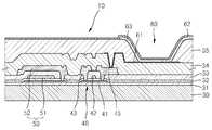
도 11을 참조하면, 상기 액티브 매트리스형의 유기 발광 디스플레이 장치(10)는 기판(500) 상에 형성된다. 상기 기판(500)은 투명한 소재, 예컨대 글래스재, 플라스틱재, 또는 금속재로 형성될 수 있다. 상기 기판(500)상에는 전체적으로 버퍼층과 같은 절연막(31)이 형성되어 있다.Referring to FIG. 11, the active matrix type organic light emitting
상기 절연막(31) 상에는 도 11에서 볼 수 있는 바와 같은 TFT(40)와, 커패시터(50)와, 유기 발광 소자(60)가 형성된다.A
상기 절연막(31)의 윗면에는 소정 패턴으로 배열된 반도체 활성층(41)이 형성되어 있다. 상기 반도체 활성층(41)은 게이트 절연막(32)에 의하여 매립되어 있다. 상기 활성층(41)은 p형 또는 n형의 반도체로 구비될 수 있다.On the upper surface of the insulating
상기 게이트 절연막(32)의 윗면에는 상기 활성층(41)과 대응되는 곳에 TFT(40)의 게이트 전극(42)이 형성된다. 그리고, 상기 게이트 전극(42)을 덮도록 층간 절연막(33)이 형성된다. 상기 층간 절연막(33)이 형성된 다음에는 드라이 에칭 등의 식각 공정에 의하여 상기 게이트 절연막(32)과 층간 절연막(33)을 식각하여 콘택 홀을 형성시켜서, 상기 활성층(41)의 일부를 드러나게 한다.A
그 다음으로, 상기 층간 절연막(33) 상에 소스/드레인 전극(43)이 형성되는 데, 콘택 홀을 통해 노출된 활성층(41)에 접촉되도록 형성된다. 상기 소스/드레인 전극(43)을 덮도록 보호막(34)이 형성되고, 식각 공정을 통하여 상기 드레인 전극(43)의 일부가 드러나도록 한다. 상기 보호막(34) 위로는 보호막(34)의 평탄화를 위해 별도의 절연막을 더 형성할 수도 있다.Next, a source /
한편, 상기 유기 발광 소자(60)는 전류의 흐름에 따라 적,녹,청색의 빛을 발광하여 소정의 화상 정보를 표시하기 위한 것으로서, 상기 보호막(34) 상에 제1 전극(61)을 형성한다. 상기 제1 전극(61)은 TFT(40)의 드레인 전극(43)과 전기적으로 연결된다.The organic
그리고, 상기 제1 전극(61)을 덮도록 화소 정의막(35)이 형성된다. 이 화소 정의막(35)에 소정의 개구를 형성한 후, 이 개구로 한정된 영역 내에 발광층을 포함하는 유기층(63)을 형성한다. 그리고 유기층(63) 위로는 제2 전극(62)을 형성한다.A
상기 화소 정의막(35)은 각 화소를 구획하는 것으로, 유기물로 형성되어, 제1 전극(61)이 형성되어 있는 기판의 표면, 특히, 보호층(34)의 표면을 평탄화한다.The
상기 제1 전극(61)과 제2 전극(62)은 서로 절연되어 있으며, 발광층을 포함하는 유기층(63)에 서로 다른 극성의 전압을 가해 발광이 이뤄지도록 한다.The
상기 발광층을 포함하는 유기층(63)은 저분자 또는 고분자 유기물이 사용될 수 있는 데, 저분자 유기물을 사용할 경우 홀 주입층(HIL: Hole Injection Layer), 홀 수송층(HTL: Hole Transport Layer), 발광층(EML: Emission Layer), 전자 수송층(ETL: Electron Transport Layer), 전자 주입층(EIL: Electron Injection Layer) 등이 단일 혹은 복합의 구조로 적층되어 형성될 수 있으며, 사용 가능한 유기 재료도 구리 프탈로시아닌(CuPc: copper phthalocyanine), N,N-디(나프탈렌-1-일)-N,N'-디페닐-벤지딘 (N,N'-Di(naphthalene-1-yl)-N,N'-diphenyl-benzidine: NPB) , 트리스-8-하이드록시퀴놀린 알루미늄(tris-8-hydroxyquinoline aluminum)(Alq3) 등을 비롯해 다양하게 적용 가능하다.When a low-molecular organic material is used, a hole injection layer (HIL), a hole transport layer (HTL), a light emitting layer (EML), a light emitting layer An electron transport layer (ETL), and an electron injection layer (EIL) may be stacked in a single or a composite structure. The usable organic material may include copper phthalocyanine (CuPc) phthalocyanine, N, N'-di (naphthalen-1-yl) -N, N'-diphenyl-benzidine ), Tris-8-hydroxyquinoline aluminum (Alq3), and the like.
이러한 유기 발광막을 형성한 후에는 제2 전극(62)을 역시 동일한 증착 공정으로 형성할 수 있다.After the organic light emitting layer is formed, the
한편, 상기 제1 전극(61)은 애노드 전극의 기능을 하고, 상기 제2 전극(62)은 캐소드 전극의 기능을 할 수 있는 데, 물론, 이들 제1 전극(61)과 제2 전극(62)의 극성은 반대로 되어도 무방하다. 그리고, 제1 전극(61)은 각 화소의 영역에 대응되도록 패터닝될 수 있고, 제2 전극(62)은 모든 화소를 덮도록 형성될 수 있다.The
상기 제1 전극(61)은 투명 전극 또는 반사형 전극으로 구비될 수 있는 데, 투명전극으로 사용될 때에는 ITO, IZO, ZnO, 또는 In2O3로 구비될 수 있고, 반사형 전극으로 사용될 때에는 Ag, Mg, Al, Pt, Pd, Au, Ni, Nd, Ir, Cr, 및 이들의 화합물 등으로 반사층을 형성한 후, 그 위에 ITO, IZO, ZnO, 또는 In2O3로 투명전극층을 형성할 수 있다. 이러한 제1 전극(61)은 스퍼터링 방법 등에 의해 성막된 후, 포토 리소그래피법 등에 의해 패터닝된다.The
한편, 상기 제2 전극(62)도 투명 전극 또는 반사형 전극으로 구비될 수 있는 데, 투명전극으로 사용될 때에는 이 제2 전극(62)이 캐소오드 전극으로 사용되므로, 일함수가 작은 금속 즉, Li, Ca, LiF/Ca, LiF/Al, Al, Ag, Mg, 및 이들의 화합물이 발광층을 포함하는 유기층(63)의 방향을 향하도록 증착한 후, 그 위에 ITO, IZO, ZnO, 또는 In2O3 등으로 보조 전극층이나 버스 전극 라인을 형성할 수 있다. 그리고, 반사형 전극으로 사용될 때에는 위 Li, Ca, LiF/Ca, LiF/Al, Al, Ag, Mg, 및 이들의 화합물을 전면 증착하여 형성한다. 이때, 증착은 전술한 발광층을 포함하는 유기층(63)의 경우와 마찬가지의 방법으로 행할 수 있다.The
본 발명은 이 외에도, 유기 TFT의 유기막 또는 무기막 등의 증착에도 사용할 수 있으며, 기타, 다양한 소재의 성막 공정에 적용 가능하다.The present invention can be used for deposition of an organic film or an inorganic film of an organic TFT or the like and can be applied to other various film forming processes.
본 명세서에서는 본 발명을 한정된 실시예를 중심으로 설명하였으나, 본 발명의 범위 내에서 다양한 실시예가 가능하다. 또한 설명되지는 않았으나, 균등한 수단도 또한 본 발명에 그대로 결합되는 것이라 할 것이다. 따라서 본 발명의 진정한 보호범위는 아래의 특허청구범위에 의하여 정해져야 할 것이다.Although the present invention has been described with reference to the limited embodiments, various embodiments are possible within the scope of the present invention. It will also be understood that, although not described, equivalent means are also incorporated into the present invention. Therefore, the true scope of protection of the present invention should be defined by the following claims.
100: 유기층 증착 어셈블리110: 증착원
120: 증착원 노즐부130: 차단판 어셈블리
150: 패터닝 슬릿 시트160: 차단 부재
170: 가열 부재500: 기판100: organic layer deposition assembly 110: evaporation source
120: evaporation source nozzle unit 130: blocking plate assembly
150: patterning slit sheet 160: blocking member
170: heating member 500: substrate
Claims (43)
Translated fromKorean증착 물질을 방사하는 증착원;
상기 증착원의 일 측에 배치되며 복수 개의 증착원 노즐들이 형성되는 증착원 노즐부;
상기 증착원 노즐부와 대향되게 배치되고 복수 개의 패터닝 슬릿들이 형성되는 패터닝 슬릿 시트;
상기 기판과 상기 증착원 사이에 배치되어 상기 기판의 적어도 일부를 가리도록 형성되는 차단 부재; 및
상기 차단 부재에 형성되어 상기 차단 부재에 소정의 열을 가하는 가열 부재;를 포함하고,
상기 기판은 상기 유기층 증착 장치와 소정 정도 이격되도록 형성되어 상기 유기층 증착 장치에 대하여 상대적으로 이동가능하도록 형성되고,
상기 차단 부재는 상기 증착원 및 상기 패터닝 슬릿 시트에 대한 위치가 고정되도록 형성되는 것을 특징으로 하는 유기층 증착 장치.An organic layer deposition apparatus for forming an organic layer on a substrate,
An evaporation source for emitting a deposition material;
An evaporation source nozzle unit disposed at one side of the evaporation source and having a plurality of evaporation source nozzles formed therein;
A patterning slit sheet disposed to face the evaporation source nozzle portion and having a plurality of patterning slits;
A blocking member disposed between the substrate and the evaporation source and configured to cover at least a part of the substrate; And
And a heating member formed on the blocking member to apply a predetermined heat to the blocking member,
Wherein the substrate is formed to be spaced apart from the organic layer deposition apparatus by a predetermined distance and relatively movable with respect to the organic layer deposition apparatus,
Wherein the blocking member is formed to be fixed in position to the evaporation source and the patterning slit sheet.
상기 차단 부재는 오픈 마스크 형상으로 구비되는 것을 특징으로 하는 유기층 증착 장치.The method according to claim 1,
Wherein the barrier member is provided in an open mask shape.
상기 차단 부재는 상기 기판의 비성막 영역을 가리도록 형성되는 것을 특징으로 하는 유기층 증착 장치.The method according to claim 1,
Wherein the blocking member is formed to cover the non-film region of the substrate.
상기 차단 부재는, 속이 빈 창틀 형상의 차단 부재 프레임 및 상기 차단 부재 프레임의 내측에 형성되는 박형의 오픈 마스크 시트를 포함하는 것을 특징으로 하는 유기층 증착 장치.The method according to claim 1,
Wherein the shielding member comprises a shielding member frame having a hollow window frame shape and a thin open mask sheet formed inside the shielding member frame.
상기 차단 부재 프레임과 상기 오픈 마스크 시트는 일체로 형성되는 것을 특징으로 하는 유기층 증착 장치.6. The method of claim 5,
Wherein the barrier member frame and the open mask sheet are integrally formed.
상기 가열 부재는 상기 차단 부재 프레임 내에 수용되는 것을 특징으로 하는 유기층 증착 장치.6. The method of claim 5,
And the heating member is accommodated in the blocking member frame.
상기 가열 부재는 상기 차단 부재 프레임에 소정의 열을 가하고, 상기 가열 부재로부터 상기 차단 부재 프레임에 가해진 열이 상기 오픈 마스크 시트로 전달되는 것을 특징으로 하는 유기층 증착 장치.6. The method of claim 5,
Wherein the heating member applies a predetermined heat to the blocking member frame, and heat applied to the blocking member frame from the heating member is transmitted to the open mask sheet.
상기 가열 부재는 상기 차단 부재를 가열하여 상기 차단 부재에 상기 증착 물질이 증착되지 아니하도록 형성되는 것을 특징으로 하는 유기층 증착 장치.The method according to claim 1,
Wherein the heating member is formed such that the evaporation material is not deposited on the blocking member by heating the blocking member.
상기 가열 부재는 상기 증착 물질의 증발 온도 이상으로 상기 차단 부재를 가열시키는 것을 특징으로 하는 유기층 증착 장치.10. The method of claim 9,
Wherein the heating member heats the blocking member at a temperature higher than the evaporation temperature of the evaporation material.
상기 가열 부재는 코일 히터 또는 박막 히터인 것을 특징으로 하는 유기층 증착 장치.The method according to claim 1,
Wherein the heating member is a coil heater or a thin film heater.
상기 유기층 증착 장치의 상기 패터닝 슬릿 시트는 상기 기판보다 작게 형성되는 것을 특징으로 하는 유기층 증착 장치.The method according to claim 1,
Wherein the patterning slit sheet of the organic layer deposition apparatus is formed to be smaller than the substrate.
상기 증착원 노즐부에는 제1 방향을 따라 복수 개의 증착원 노즐들이 형성되고,
상기 패터닝 슬릿 시트에는 상기 제1 방향에 대해 수직인 제2 방향을 따라 복수 개의 패터닝 슬릿들이 형성되는 것을 특징으로 하는 유기층 증착 장치.The method according to claim 1,
A plurality of evaporation source nozzles are formed in the evaporation source nozzle portion along a first direction,
Wherein the patterning slit sheet is formed with a plurality of patterning slits along a second direction perpendicular to the first direction.
상기 증착원 및 상기 증착원 노즐부와 상기 패터닝 슬릿 시트는 연결 부재에 의해 결합되어 일체로 형성되는 것을 특징으로 하는 유기층 증착 장치.14. The method of claim 13,
Wherein the evaporation source, the evaporation source nozzle unit, and the patterning slit sheet are integrally formed by a coupling member.
상기 연결 부재는 상기 증착 물질의 이동 경로를 가이드 하는 것을 특징으로 하는 유기층 증착 장치.15. The method of claim 14,
Wherein the connection member guides the movement path of the deposition material.
상기 연결 부재는 상기 증착원 및 상기 증착원 노즐부와 상기 패터닝 슬릿 시트 사이의 공간을 외부로부터 밀폐하도록 형성되는 것을 특징으로 하는 유기층 증착 장치.16. The method of claim 15,
Wherein the connection member is formed to seal the space between the evaporation source and the evaporation source nozzle portion and the patterning slit sheet from the outside.
상기 복수 개의 증착원 노즐들은 소정 각도 틸트 되도록 형성되는 것을 특징으로 하는 유기층 증착 장치.14. The method of claim 13,
Wherein the plurality of evaporation source nozzles are formed to be tilted by a predetermined angle.
상기 복수 개의 증착원 노즐들은 상기 제1 방향을 따라 형성된 두 열(列)의 증착원 노즐들을 포함하며, 상기 두 열(列)의 증착원 노즐들은 서로 마주보는 방향으로 틸트되어 있는 것을 특징으로 하는 유기층 증착 장치.18. The method of claim 17,
Wherein the plurality of evaporation source nozzles include two rows of evaporation source nozzles formed along the first direction and the evaporation source nozzles of the two rows are tilted in directions opposite to each other. Organic layer deposition apparatus.
상기 복수 개의 증착원 노즐들은 상기 제1 방향을 따라 형성된 두 열(列)의 증착원 노즐들을 포함하며,
상기 두 열(列)의 증착원 노즐들 중 제1 측에 배치된 증착원 노즐들은 패터닝 슬릿 시트의 제2 측 단부를 바라보도록 배치되고,
상기 두 열(列)의 증착원 노즐들 중 제2 측에 배치된 증착원 노즐들은 패터닝 슬릿 시트의 제1 측 단부를 바라보도록 배치되는 것을 특징으로 하는 유기층 증착 장치.18. The method of claim 17,
Wherein the plurality of evaporation source nozzles include two rows of evaporation source nozzles formed along the first direction,
The evaporation source nozzles disposed on the first one of the two rows of the evaporation source rows are arranged to face the second side edge of the patterning slit sheet,
Wherein the evaporation source nozzles disposed on the second side of the two rows of the evaporation source rows are arranged to face the first side end of the patterning slit sheet.
상기 증착원 노즐부에는 제1 방향을 따라 복수 개의 증착원 노즐들이 형성되고,
상기 패터닝 슬릿 시트에는 상기 제1 방향을 따라 복수 개의 패터닝 슬릿들이 형성되고,
상기 유기층 증착 장치는, 상기 증착원 노즐부와 상기 패터닝 슬릿 시트 사이에 상기 제1 방향을 따라 배치되어, 상기 증착원 노즐부와 상기 패터닝 슬릿 시트 사이의 공간을 복수 개의 증착 공간들로 구획하는 복수 개의 차단판들을 구비하는 차단판 어셈블리;를 더 포함하는 유기층 증착 장치.The method according to claim 1,
A plurality of evaporation source nozzles are formed in the evaporation source nozzle portion along a first direction,
A plurality of patterning slits are formed in the patterning slit sheet along the first direction,
Wherein the organic layer deposition apparatus includes a plurality of deposition spaces arranged along the first direction between the deposition source nozzle section and the patterning slit sheet and partitioning the space between the deposition source nozzle section and the patterning slit sheet into a plurality of deposition spaces And a blocking plate assembly having a plurality of blocking plates.
상기 복수 개의 차단판들 각각은 상기 제1 방향과 수직인 제2 방향을 따라 연장되도록 형성된 것을 특징으로 하는 유기층 증착 장치.21. The method of claim 20,
Wherein each of the plurality of blocking plates is formed to extend along a second direction perpendicular to the first direction.
상기 차단판 어셈블리는 복수 개의 제1 차단판들을 구비하는 제1 차단판 어셈블리와, 복수 개의 제2 차단판들을 구비하는 제2 차단판 어셈블리를 포함하는 것을 특징으로 하는 유기층 증착 장치.21. The method of claim 20,
Wherein the blocking plate assembly includes a first blocking plate assembly having a plurality of first blocking plates, and a second blocking plate assembly having a plurality of second blocking plates.
상기 복수 개의 제1 차단판들 및 상기 복수 개의 제2 차단판들 각각은 상기 제1 방향과 수직인 제2 방향으로 형성되어, 상기 증착원 노즐부와 상기 패터닝 슬릿 시트 사이의 공간을 복수 개의 증착 공간들로 구획하는 것을 특징으로 하는 유기층 증착 장치.23. The method of claim 22,
Wherein the plurality of first blocking plates and the plurality of second blocking plates are formed in a second direction perpendicular to the first direction so that a space between the evaporation source nozzle portion and the patterning slit sheet is formed by a plurality of deposition Wherein the organic layer is partitioned into spaces.
상기 유기층 증착 장치는 챔버를 더 포함하고,
상기 증착원 노즐부에는 제1 방향을 따라 복수 개의 증착원 노즐들이 형성되고,
상기 패터닝 슬릿 시트는 상기 챔버의 내측에 고정 결합되며, 상기 제1 방향에 대해 수직인 제2 방향을 따라 복수 개의 패터닝 슬릿들이 형성되는 것을 특징으로 하는 유기층 증착 장치.The method according to claim 1,
Wherein the organic layer deposition apparatus further comprises a chamber,
A plurality of evaporation source nozzles are formed in the evaporation source nozzle portion along a first direction,
Wherein the patterning slit sheet is fixedly coupled to the inside of the chamber and a plurality of patterning slits are formed along a second direction perpendicular to the first direction.
상기 기판이 고정된 정전척을 상기 제1 방향을 따라 이동시키는 제1 순환부를 더 포함하는 유기층 증착 장치.25. The method of claim 24,
And a first circulation unit for moving the electrostatic chuck having the substrate fixed thereto along the first direction.
상기 제1 순환부는,
내부에 상기 증착원이 수용되는 프레임; 및
상기 프레임의 내측면으로부터 돌출 형성되어 상기 패터닝 슬릿 시트를 지지하는 시트 지지대;를 포함하는 유기층 증착 장치.26. The method of claim 25,
The first circulation unit includes:
A frame in which the evaporation source is accommodated; And
And a sheet support protruding from an inner surface of the frame to support the patterning slit sheet.
상기 기판을 정전척으로 고정시키는 로딩부; 및
상기 정전척으로부터 증착이 완료된 상기 기판을 분리시키는 언로딩부;를 더 포함하는 유기층 증착 장치.26. The method of claim 25,
A loading unit for fixing the substrate by an electrostatic chuck; And
And an unloading unit for separating the substrate from which the deposition is completed from the electrostatic chuck.
상기 유기층 증착 장치와 상기 기판 중 어느 일 측이 타 측에 대하여 상대적으로 이동하면서, 상기 유기층 증착 장치에서 방사되는 증착 물질이 상기 기판상에 증착되는 단계;를 포함하고,
상기 차단 부재는 상기 증착원 및 상기 패터닝 슬릿 시트에 대한 위치가 고정되도록 형성되는 것을 특징으로 하는 유기 발광 디스플레이 장치의 제조방법.A deposition source nozzle unit disposed at one side of the deposition source and configured to form a plurality of deposition source nozzles; a patterning slit sheet disposed opposite to the deposition source nozzle unit and having a plurality of patterning slits; An organic layer deposition apparatus including a barrier member disposed between the substrate and the evaporation source and configured to cover at least a part of the substrate, and a heating member formed on the barrier member and applying a predetermined heat to the barrier member, The substrate being spaced apart from the substrate by a predetermined distance; And
And depositing a deposition material to be emitted from the organic layer deposition apparatus on the substrate while moving either one of the organic layer deposition apparatus and the substrate relative to the other side,
Wherein the blocking member is formed to be fixed in position to the evaporation source and the patterning slit sheet.
상기 차단 부재는 오픈 마스크 형상으로 구비되는 것을 특징으로 하는 유기 발광 디스플레이 장치의 제조방법.29. The method of claim 28,
Wherein the blocking member is provided in an open-mask shape.
상기 차단 부재는 상기 기판의 비성막 영역을 가리도록 형성되는 것을 특징으로 하는 유기 발광 디스플레이 장치의 제조방법.29. The method of claim 28,
Wherein the blocking member is formed to cover the non-deposition region of the substrate.
상기 차단 부재는, 속이 빈 창틀 형상의 차단 부재 프레임 및 상기 차단 부재 프레임의 내측에 형성되는 박형의 오픈 마스크 시트를 포함하는 것을 특징으로 하는 유기 발광 디스플레이 장치의 제조방법.29. The method of claim 28,
Wherein the shielding member comprises a shielding member frame having a hollow window frame shape and a thin open mask sheet formed inside the shielding member frame.
상기 차단 부재 프레임과 상기 오픈 마스크 시트는 일체로 형성되는 것을 특징으로 하는 유기 발광 디스플레이 장치의 제조방법.33. The method of claim 32,
Wherein the barrier member frame and the open mask sheet are integrally formed.
상기 가열 부재는 상기 차단 부재 프레임 내에 수용되는 것을 특징으로 하는 유기 발광 디스플레이 장치의 제조방법.33. The method of claim 32,
And the heating member is received in the blocking member frame.
상기 가열 부재는 상기 차단 부재 프레임에 소정의 열을 가하고, 상기 가열 부재로부터 상기 차단 부재 프레임에 가해진 열이 상기 오픈 마스크 시트로 전달되는 것을 특징으로 하는 유기 발광 디스플레이 장치의 제조방법.33. The method of claim 32,
Wherein the heating member applies a predetermined heat to the blocking member frame, and heat applied to the blocking member frame from the heating member is transmitted to the open mask sheet.
상기 가열 부재는 상기 차단 부재를 가열하여 상기 차단 부재에 상기 증착 물질이 증착되지 아니하도록 형성되는 것을 특징으로 하는 유기 발광 디스플레이 장치의 제조방법.29. The method of claim 28,
Wherein the heating member is formed such that the evaporation material is not deposited on the blocking member by heating the blocking member.
상기 가열 부재는 상기 증착 물질의 증발 온도 이상으로 상기 차단 부재를 가열시키는 것을 특징으로 하는 유기 발광 디스플레이 장치의 제조방법.37. The method of claim 36,
Wherein the heating member heats the blocking member at a temperature equal to or higher than an evaporation temperature of the evaporation material.
상기 가열 부재는 코일 히터 또는 박막 히터인 것을 특징으로 하는 유기 발광 디스플레이 장치의 제조방법.29. The method of claim 28,
Wherein the heating member is a coil heater or a thin film heater.
상기 유기층 증착 장치의 상기 패터닝 슬릿 시트는 상기 기판보다 작게 형성되는 것을 특징으로 하는 유기 발광 디스플레이 장치의 제조방법.29. The method of claim 28,
Wherein the patterning slit sheet of the organic layer deposition apparatus is formed to be smaller than the substrate.
상기 증착원 노즐부에는 제1 방향을 따라 복수 개의 증착원 노즐들이 형성되고,
상기 패터닝 슬릿 시트에는 상기 제1 방향에 대해 수직인 제2 방향을 따라 복수 개의 패터닝 슬릿들이 형성되는 것을 특징으로 하는 유기 발광 디스플레이 장치의 제조방법.29. The method of claim 28,
A plurality of evaporation source nozzles are formed in the evaporation source nozzle portion along a first direction,
Wherein the patterning slit sheet is formed with a plurality of patterning slits along a second direction perpendicular to the first direction.
상기 증착원 노즐부에는 제1 방향을 따라 복수 개의 증착원 노즐들이 형성되고,
상기 패터닝 슬릿 시트에는 상기 제1 방향을 따라 복수 개의 패터닝 슬릿들이 형성되고,
상기 유기층 증착 장치는, 상기 증착원 노즐부와 상기 패터닝 슬릿 시트 사이에 상기 제1 방향을 따라 배치되어, 상기 증착원 노즐부와 상기 패터닝 슬릿 시트 사이의 공간을 복수 개의 증착 공간들로 구획하는 복수 개의 차단판들을 구비하는 차단판 어셈블리;를 더 포함하는 유기 발광 디스플레이 장치의 제조방법.29. The method of claim 28,
A plurality of evaporation source nozzles are formed in the evaporation source nozzle portion along a first direction,
A plurality of patterning slits are formed in the patterning slit sheet along the first direction,
Wherein the organic layer deposition apparatus includes a plurality of deposition spaces arranged along the first direction between the deposition source nozzle section and the patterning slit sheet and partitioning the space between the deposition source nozzle section and the patterning slit sheet into a plurality of deposition spaces And a blocking plate assembly having a plurality of blocking plates.
상기 유기층 증착 장치는 챔버를 더 포함하고,
상기 증착원 노즐부에는 제1 방향을 따라 복수 개의 증착원 노즐들이 형성되고,
상기 패터닝 슬릿 시트는 상기 챔버의 내측에 고정 결합되며, 상기 제1 방향에 대해 수직인 제2 방향을 따라 복수 개의 패터닝 슬릿들이 형성되는 것을 특징으로 하는 유기 발광 디스플레이 장치의 제조방법.29. The method of claim 28,
Wherein the organic layer deposition apparatus further comprises a chamber,
A plurality of evaporation source nozzles are formed in the evaporation source nozzle portion along a first direction,
Wherein the patterning slit sheet is fixedly coupled to the inside of the chamber and a plurality of patterning slits are formed along a second direction perpendicular to the first direction.
Priority Applications (2)
| Application Number | Priority Date | Filing Date | Title |
|---|---|---|---|
| KR1020110049794AKR101852517B1 (en) | 2011-05-25 | 2011-05-25 | Apparatus for organic layer deposition and method for manufacturing of organic light emitting display apparatus using the same |
| US13/470,077US9249493B2 (en) | 2011-05-25 | 2012-05-11 | Organic layer deposition apparatus and method of manufacturing organic light-emitting display apparatus by using the same |
Applications Claiming Priority (1)
| Application Number | Priority Date | Filing Date | Title |
|---|---|---|---|
| KR1020110049794AKR101852517B1 (en) | 2011-05-25 | 2011-05-25 | Apparatus for organic layer deposition and method for manufacturing of organic light emitting display apparatus using the same |
Publications (2)
| Publication Number | Publication Date |
|---|---|
| KR20120131547A KR20120131547A (en) | 2012-12-05 |
| KR101852517B1true KR101852517B1 (en) | 2018-04-27 |
Family
ID=47219476
Family Applications (1)
| Application Number | Title | Priority Date | Filing Date |
|---|---|---|---|
| KR1020110049794AActiveKR101852517B1 (en) | 2011-05-25 | 2011-05-25 | Apparatus for organic layer deposition and method for manufacturing of organic light emitting display apparatus using the same |
Country Status (2)
| Country | Link |
|---|---|
| US (1) | US9249493B2 (en) |
| KR (1) | KR101852517B1 (en) |
Families Citing this family (31)
| Publication number | Priority date | Publication date | Assignee | Title |
|---|---|---|---|---|
| US8882920B2 (en)* | 2009-06-05 | 2014-11-11 | Samsung Display Co., Ltd. | Thin film deposition apparatus |
| JP5328726B2 (en) | 2009-08-25 | 2013-10-30 | 三星ディスプレイ株式會社 | Thin film deposition apparatus and organic light emitting display device manufacturing method using the same |
| JP5677785B2 (en) | 2009-08-27 | 2015-02-25 | 三星ディスプレイ株式會社Samsung Display Co.,Ltd. | Thin film deposition apparatus and organic light emitting display device manufacturing method using the same |
| US8876975B2 (en) | 2009-10-19 | 2014-11-04 | Samsung Display Co., Ltd. | Thin film deposition apparatus |
| KR101084184B1 (en) | 2010-01-11 | 2011-11-17 | 삼성모바일디스플레이주식회사 | Thin film deposition apparatus |
| KR101193186B1 (en) | 2010-02-01 | 2012-10-19 | 삼성디스플레이 주식회사 | Apparatus for thin layer deposition, method for manufacturing of organic light emitting display apparatus using the same, and organic light emitting display apparatus manufactured by the method |
| KR101156441B1 (en) | 2010-03-11 | 2012-06-18 | 삼성모바일디스플레이주식회사 | Apparatus for thin layer deposition |
| US8894458B2 (en) | 2010-04-28 | 2014-11-25 | Samsung Display Co., Ltd. | Thin film deposition apparatus, method of manufacturing organic light-emitting display device by using the apparatus, and organic light-emitting display device manufactured by using the method |
| KR101223723B1 (en) | 2010-07-07 | 2013-01-18 | 삼성디스플레이 주식회사 | Apparatus for thin layer deposition, method for manufacturing of organic light emitting display apparatus using the same, and organic light emitting display apparatus manufactured by the method |
| KR101723506B1 (en) | 2010-10-22 | 2017-04-19 | 삼성디스플레이 주식회사 | Apparatus for organic layer deposition and method for manufacturing of organic light emitting display apparatus using the same |
| KR101738531B1 (en) | 2010-10-22 | 2017-05-23 | 삼성디스플레이 주식회사 | Method for manufacturing of organic light emitting display apparatus, and organic light emitting display apparatus manufactured by the method |
| KR20120045865A (en) | 2010-11-01 | 2012-05-09 | 삼성모바일디스플레이주식회사 | Apparatus for organic layer deposition |
| KR20120065789A (en) | 2010-12-13 | 2012-06-21 | 삼성모바일디스플레이주식회사 | Apparatus for organic layer deposition |
| KR101760897B1 (en) | 2011-01-12 | 2017-07-25 | 삼성디스플레이 주식회사 | Deposition source and apparatus for organic layer deposition having the same |
| KR101840654B1 (en) | 2011-05-25 | 2018-03-22 | 삼성디스플레이 주식회사 | Apparatus for organic layer deposition and method for manufacturing of organic light emitting display apparatus using the same |
| KR101852517B1 (en) | 2011-05-25 | 2018-04-27 | 삼성디스플레이 주식회사 | Apparatus for organic layer deposition and method for manufacturing of organic light emitting display apparatus using the same |
| KR101857249B1 (en) | 2011-05-27 | 2018-05-14 | 삼성디스플레이 주식회사 | Patterning slit sheet assembly, apparatus for organic layer deposition, method for manufacturing organic light emitting display apparatus and organic light emitting display apparatus |
| KR101826068B1 (en) | 2011-07-04 | 2018-02-07 | 삼성디스플레이 주식회사 | Apparatus for thin layer deposition |
| KR102013318B1 (en)* | 2012-09-20 | 2019-08-23 | 삼성디스플레이 주식회사 | Apparatus for thin layer deposition, method for manufacturing of organic light emitting display apparatus using the same, and organic light emitting display apparatus |
| KR102075527B1 (en) | 2013-05-16 | 2020-02-11 | 삼성디스플레이 주식회사 | Apparatus for organic layer deposition, and method for manufacturing of organic light emitting display apparatus using the same |
| KR102080010B1 (en)* | 2013-06-04 | 2020-02-24 | 삼성디스플레이 주식회사 | Apparatus for thin film depositon and method for manufacturing of orgarnic light emitting display apparatus using the same |
| JP2015069806A (en)* | 2013-09-27 | 2015-04-13 | 株式会社ジャパンディスプレイ | Manufacturing method for organic electroluminescent display device |
| KR102160157B1 (en) | 2014-01-13 | 2020-09-28 | 삼성디스플레이 주식회사 | Organic light-emitting display apparatus and method for manufacturing the same |
| US20150211106A1 (en)* | 2014-01-30 | 2015-07-30 | Areesys Corporation | Apparatus for depositing thin films of organic materials |
| KR102254582B1 (en) | 2014-10-02 | 2021-05-24 | 삼성디스플레이 주식회사 | Organic light emitting display device and method of manufacturing the same |
| KR102356353B1 (en)* | 2015-07-07 | 2022-01-27 | 삼성디스플레이 주식회사 | Deposition device and method of manufacturing display device using the same |
| KR102526350B1 (en)* | 2015-11-19 | 2023-04-27 | 삼성디스플레이 주식회사 | Appratus for manufacturing display device |
| KR102488145B1 (en)* | 2017-05-30 | 2023-01-17 | 삼성디스플레이 주식회사 | Apparatus for cleaning mask and method of mask cleaning |
| CN107177818B (en)* | 2017-07-19 | 2019-05-21 | 武汉天马微电子有限公司 | Mask plate for organic material evaporation |
| CN112575308B (en)* | 2019-09-29 | 2023-03-24 | 宝山钢铁股份有限公司 | Vacuum coating device capable of efficiently coating strip steel under vacuum |
| CN110694844B (en)* | 2019-11-05 | 2021-06-25 | 泰安盛源电气有限公司 | Electric cabinet pretreatment line and treatment process |
Family Cites Families (450)
| Publication number | Priority date | Publication date | Assignee | Title |
|---|---|---|---|---|
| JPS6053745B2 (en) | 1981-07-31 | 1985-11-27 | アルバツク成膜株式会社 | Method for forming heterogeneous optical thin films by binary deposition |
| JPS5959237U (en) | 1982-10-15 | 1984-04-18 | 鐘通工業株式会社 | Switchable permanent magnetic chuck |
| KR890002747B1 (en) | 1983-11-07 | 1989-07-26 | 가부시기가이샤 히다찌세이사꾸쇼 | Film deposition method using ion beam and apparatus therefor |
| JPH0682642B2 (en) | 1985-08-09 | 1994-10-19 | 株式会社日立製作所 | Surface treatment equipment |
| US4792378A (en) | 1987-12-15 | 1988-12-20 | Texas Instruments Incorporated | Gas dispersion disk for use in plasma enhanced chemical vapor deposition reactor |
| JPH02247372A (en) | 1989-03-17 | 1990-10-03 | Mitsubishi Electric Corp | Thin film deposition method |
| JP3125279B2 (en) | 1991-02-25 | 2001-01-15 | 東海カーボン株式会社 | Graphite crucible for vacuum evaporation |
| JP2572861Y2 (en) | 1991-05-13 | 1998-05-25 | テイエチケー株式会社 | Slide unit for linear motion |
| JP2797233B2 (en) | 1992-07-01 | 1998-09-17 | 富士通株式会社 | Thin film growth equipment |
| FR2695943B1 (en) | 1992-09-18 | 1994-10-14 | Alsthom Cge Alcatel | Process for the vapor phase deposition of a fluorinated glass film on a substrate. |
| JP3395801B2 (en) | 1994-04-28 | 2003-04-14 | 株式会社ニコン | Catadioptric projection optical system, scanning projection exposure apparatus, and scanning projection exposure method |
| JP3401356B2 (en) | 1995-02-21 | 2003-04-28 | パイオニア株式会社 | Organic electroluminescent display panel and method of manufacturing the same |
| JPH1050478A (en) | 1996-04-19 | 1998-02-20 | Toray Ind Inc | Organic electroluminescent device and method of manufacturing the same |
| CH691680A5 (en) | 1996-10-15 | 2001-09-14 | Unaxis Deutschland Gmbh | Transport apparatus for workpieces in a vacuum system. |
| US6091195A (en) | 1997-02-03 | 2000-07-18 | The Trustees Of Princeton University | Displays having mesa pixel configuration |
| US6274198B1 (en) | 1997-02-24 | 2001-08-14 | Agere Systems Optoelectronics Guardian Corp. | Shadow mask deposition |
| JPH10270535A (en) | 1997-03-25 | 1998-10-09 | Nikon Corp | Moving stage device and circuit device manufacturing method using the stage device |
| KR100257219B1 (en) | 1997-10-23 | 2000-05-15 | 박용관 | Method and device for making a safety operation of a polyethylene gas pipe valve arrangement |
| JP3948082B2 (en) | 1997-11-05 | 2007-07-25 | カシオ計算機株式会社 | Method for manufacturing organic electroluminescence element |
| US6337102B1 (en) | 1997-11-17 | 2002-01-08 | The Trustees Of Princeton University | Low pressure vapor phase deposition of organic thin films |
| US6099649A (en) | 1997-12-23 | 2000-08-08 | Applied Materials, Inc. | Chemical vapor deposition hot-trap for unreacted precursor conversion and effluent removal |
| JP2000068054A (en) | 1998-08-26 | 2000-03-03 | Hokuriku Electric Ind Co Ltd | Manufacture of el element |
| US6280821B1 (en) | 1998-09-10 | 2001-08-28 | Ppg Industries Ohio, Inc. | Reusable mask and method for coating substrate |
| US6384529B2 (en) | 1998-11-18 | 2002-05-07 | Eastman Kodak Company | Full color active matrix organic electroluminescent display panel having an integrated shadow mask |
| US6222198B1 (en) | 1998-11-20 | 2001-04-24 | Mems Optical Inc. | System and method for aligning pattern areas on opposing substrate surfaces |
| CA2374448A1 (en) | 1999-01-26 | 2000-08-03 | Dbs Beschichtung Und Systeme-Technik Gmbh | Method for coating the inside of pipes and coating system |
| JP3734239B2 (en) | 1999-04-02 | 2006-01-11 | キヤノン株式会社 | Organic film vacuum deposition mask regeneration method and apparatus |
| US6610150B1 (en) | 1999-04-02 | 2003-08-26 | Asml Us, Inc. | Semiconductor wafer processing system with vertically-stacked process chambers and single-axis dual-wafer transfer system |
| KR20000019254U (en) | 1999-04-07 | 2000-11-06 | 손대균 | Roundin WheeL |
| JP4136185B2 (en) | 1999-05-12 | 2008-08-20 | パイオニア株式会社 | Organic electroluminescent multicolor display and method for manufacturing the same |
| US6469439B2 (en) | 1999-06-15 | 2002-10-22 | Toray Industries, Inc. | Process for producing an organic electroluminescent device |
| EP1115268A1 (en) | 1999-07-07 | 2001-07-11 | Sony Corporation | Method and apparatus for manufacturing flexible organic el display |
| JP2001052862A (en) | 1999-08-04 | 2001-02-23 | Hokuriku Electric Ind Co Ltd | Manufacture of organic el element and device therefor |
| JP4352522B2 (en) | 1999-09-01 | 2009-10-28 | ソニー株式会社 | Light-emitting flat display element |
| JP4187367B2 (en) | 1999-09-28 | 2008-11-26 | 三洋電機株式会社 | ORGANIC LIGHT EMITTING ELEMENT, ITS MANUFACTURING DEVICE, AND ITS MANUFACTURING METHOD |
| KR20010050711A (en) | 1999-09-29 | 2001-06-15 | 준지 키도 | Organic electroluminescent device, group of organic electroluminescent devices and controlling method of emission spectrum in such devices |
| KR20010039298A (en) | 1999-10-29 | 2001-05-15 | 김영남 | Field emission display |
| WO2001030404A1 (en) | 1999-10-29 | 2001-05-03 | E. One Co., Ltd. | Scent diffusion apparatus and method thereof |
| KR100302159B1 (en) | 1999-10-29 | 2001-09-22 | 최중호 | Scent diffusion apparatus and method therefor |
| KR100388903B1 (en) | 1999-12-10 | 2003-06-25 | 삼성에스디아이 주식회사 | Shadow mask frame assembly for the flat CRT |
| JP2001185350A (en) | 1999-12-24 | 2001-07-06 | Sanyo Electric Co Ltd | Worn mask, its manufacturing method, electroluminescent display device and its manufacturing method |
| TW490714B (en) | 1999-12-27 | 2002-06-11 | Semiconductor Energy Lab | Film formation apparatus and method for forming a film |
| KR100653515B1 (en) | 1999-12-30 | 2006-12-04 | 주식회사 팬택앤큐리텔 | Terminal of mobile communication system |
| JP3754859B2 (en) | 2000-02-16 | 2006-03-15 | キヤノン株式会社 | Manufacturing method of image display device |
| KR20010092914A (en) | 2000-03-27 | 2001-10-27 | 윤종용 | Electrical static chuck comprising a shadow ring |
| JP3802309B2 (en) | 2000-03-28 | 2006-07-26 | 株式会社アドテックエンジニアリング | Positioning apparatus and exposure apparatus in multilayer circuit board manufacture |
| JP4053209B2 (en) | 2000-05-01 | 2008-02-27 | 三星エスディアイ株式会社 | Manufacturing method of organic EL display |
| TW593622B (en) | 2000-05-19 | 2004-06-21 | Eastman Kodak Co | Method of using predoped materials for making an organic light-emitting device |
| EP1167566B1 (en) | 2000-06-22 | 2011-01-26 | Panasonic Electric Works Co., Ltd. | Apparatus for and method of vacuum vapor deposition |
| KR20020000201A (en) | 2000-06-23 | 2002-01-05 | 최승락 | Method cleaning Liquid Chrystal Display using Laser and Vapor Phase |
| TW451601B (en) | 2000-08-07 | 2001-08-21 | Ind Tech Res Inst | The fabrication method of full color organic electroluminescent device |
| JP2002175878A (en) | 2000-09-28 | 2002-06-21 | Sanyo Electric Co Ltd | Layer forming method and color light emitting device manufacturing method |
| TW594395B (en) | 2000-09-29 | 2004-06-21 | Nippon Zeon Co | Photoresist composition for insulating film, insulating film for organic electroluminescent element, and process for producing the same |
| KR100726132B1 (en) | 2000-10-31 | 2007-06-12 | 엘지.필립스 엘시디 주식회사 | Array substrate for liquid crystal display device and manufacturing method |
| US7078070B2 (en) | 2000-11-07 | 2006-07-18 | Helix Technology Inc. | Method for fabricating an organic light emitting diode |
| US6468496B2 (en) | 2000-12-21 | 2002-10-22 | Arco Chemical Technology, L.P. | Process for producing hydrogen peroxide |
| KR100625403B1 (en) | 2000-12-22 | 2006-09-18 | 주식회사 하이닉스반도체 | Virtual Channel SDRAM |
| KR100698033B1 (en) | 2000-12-29 | 2007-03-23 | 엘지.필립스 엘시디 주식회사 | Organic electroluminescent device and manufacturing method thereof |
| US6558735B2 (en) | 2001-04-20 | 2003-05-06 | Eastman Kodak Company | Reusable mass-sensor in manufacture of organic light-emitting devices |
| KR100405080B1 (en) | 2001-05-11 | 2003-11-10 | 엘지.필립스 엘시디 주식회사 | A method of crystallizing Si |
| KR100463212B1 (en) | 2001-05-19 | 2004-12-23 | 주식회사 아이엠티 | Apparatus for dry surface-cleaning of materials |
| JP4704605B2 (en) | 2001-05-23 | 2011-06-15 | 淳二 城戸 | Continuous vapor deposition apparatus, vapor deposition apparatus and vapor deposition method |
| KR20020091457A (en) | 2001-05-30 | 2002-12-06 | 주식회사 현대 디스플레이 테크놀로지 | Method for control color property of tft-lcd |
| US20020197393A1 (en) | 2001-06-08 | 2002-12-26 | Hideaki Kuwabara | Process of manufacturing luminescent device |
| JP2003003250A (en) | 2001-06-22 | 2003-01-08 | Alps Electric Co Ltd | Vacuum deposition polymerization system and method for depositing organic film using the system |
| JP2003077662A (en) | 2001-06-22 | 2003-03-14 | Junji Kido | Method and device for manufacturing organic electroluminescent element |
| KR100406059B1 (en) | 2001-06-22 | 2003-11-17 | 미래산업 주식회사 | Transfer for Tray Feeder |
| KR100732742B1 (en) | 2001-06-27 | 2007-06-27 | 주식회사 하이닉스반도체 | Focus monitoring method |
| US6483690B1 (en) | 2001-06-28 | 2002-11-19 | Lam Research Corporation | Ceramic electrostatic chuck assembly and method of making |
| US6554969B1 (en) | 2001-07-11 | 2003-04-29 | Advanced Micro Devices, Inc. | Acoustically enhanced deposition processes, and systems for performing same |
| JP3705237B2 (en) | 2001-09-05 | 2005-10-12 | ソニー株式会社 | Display device manufacturing system and method using organic electroluminescent element |
| KR200257218Y1 (en) | 2001-09-07 | 2001-12-24 | 엘지.필립스 엘시디 주식회사 | Mask apparatus for organic electro-luminescence device |
| KR100437768B1 (en) | 2001-09-13 | 2004-06-30 | 엘지전자 주식회사 | Thin Film Sputtering Device |
| US20090208754A1 (en) | 2001-09-28 | 2009-08-20 | Vitex Systems, Inc. | Method for edge sealing barrier films |
| TW591202B (en) | 2001-10-26 | 2004-06-11 | Hermosa Thin Film Co Ltd | Dynamic film thickness control device/method and ITS coating method |
| KR100730111B1 (en) | 2001-10-26 | 2007-06-19 | 삼성에스디아이 주식회사 | Frame for mask of organic EL element |
| KR100430336B1 (en) | 2001-11-16 | 2004-05-03 | 정광호 | Apparatus for manufacturing organic electro-luminescent light emitting devices for mass production |
| KR100450978B1 (en) | 2001-11-26 | 2004-10-02 | 주성엔지니어링(주) | electrostatic chuck |
| US20030101937A1 (en) | 2001-11-28 | 2003-06-05 | Eastman Kodak Company | Thermal physical vapor deposition source for making an organic light-emitting device |
| JP2003159786A (en) | 2001-11-28 | 2003-06-03 | Seiko Epson Corp | Discharge method and apparatus, electro-optical apparatus, method for manufacturing the same and apparatus for manufacturing the same, color filter, method for manufacturing the same and apparatus for manufacturing the same, device having base material, method for manufacturing the same, and apparatus for manufacturing the same |
| KR100490534B1 (en) | 2001-12-05 | 2005-05-17 | 삼성에스디아이 주식회사 | Mask frame assembly for thin layer vacuum evaporation of Organic electro luminescence device |
| SG114589A1 (en) | 2001-12-12 | 2005-09-28 | Semiconductor Energy Lab | Film formation apparatus and film formation method and cleaning method |
| TW200305773A (en) | 2001-12-26 | 2003-11-01 | Pentax Corp | Projection Aligner |
| US20090169868A1 (en) | 2002-01-29 | 2009-07-02 | Vanderbilt University | Methods and apparatus for transferring a material onto a substrate using a resonant infrared pulsed laser |
| US6919139B2 (en) | 2002-02-14 | 2005-07-19 | E. I. Du Pont De Nemours And Company | Electroluminescent iridium compounds with phosphinoalkoxides and phenylpyridines or phenylpyrimidines and devices made with such compounds |
| US6897164B2 (en) | 2002-02-14 | 2005-05-24 | 3M Innovative Properties Company | Aperture masks for circuit fabrication |
| US7006202B2 (en) | 2002-02-21 | 2006-02-28 | Lg.Philips Lcd Co., Ltd. | Mask holder for irradiating UV-rays |
| KR100595310B1 (en) | 2002-02-22 | 2006-07-03 | 엘지.필립스 엘시디 주식회사 | Mask Fixing Device and Checking Device Using It |
| US20030168013A1 (en) | 2002-03-08 | 2003-09-11 | Eastman Kodak Company | Elongated thermal physical vapor deposition source with plural apertures for making an organic light-emitting device |
| JP2003297562A (en) | 2002-03-29 | 2003-10-17 | Sanyo Electric Co Ltd | Vapor deposition method |
| KR100501306B1 (en) | 2002-04-01 | 2005-07-18 | (주) 휴네텍 | method of manufacturing a light guiding panel and an apparatus for the same, and a particle blasting apparatus for manufacturing the light guiding panel |
| KR100469252B1 (en) | 2002-04-12 | 2005-02-02 | 엘지전자 주식회사 | Shadow Mask and Full Color Organic Electroluminescence Display Device Using the same |
| US6749906B2 (en)* | 2002-04-25 | 2004-06-15 | Eastman Kodak Company | Thermal physical vapor deposition apparatus with detachable vapor source(s) and method |
| JP2003321767A (en) | 2002-04-26 | 2003-11-14 | Seiko Epson Corp | Method for depositing thin film, organic electroluminescence device, method for manufacturing organic electroluminescence device, and electronic equipment |
| ATE481982T1 (en) | 2002-05-03 | 2010-10-15 | Us Gov Health & Human Serv | DENGUE VACCINE WITH A COMMON 30 NUCLEOTIDE DELETION IN THE 3'UTR OF DENGUE TYPES 1 AND 2. |
| US20030232563A1 (en) | 2002-05-09 | 2003-12-18 | Isao Kamiyama | Method and apparatus for manufacturing organic electroluminescence device, and system and method for manufacturing display unit using organic electroluminescence devices |
| JP4292777B2 (en) | 2002-06-17 | 2009-07-08 | ソニー株式会社 | Thin film forming equipment |
| US6955726B2 (en) | 2002-06-03 | 2005-10-18 | Samsung Sdi Co., Ltd. | Mask and mask frame assembly for evaporation |
| US20030221620A1 (en) | 2002-06-03 | 2003-12-04 | Semiconductor Energy Laboratory Co., Ltd. | Vapor deposition device |
| KR100908232B1 (en) | 2002-06-03 | 2009-07-20 | 삼성모바일디스플레이주식회사 | Mask frame assembly for thin film deposition of organic electroluminescent device |
| JP2004086136A (en) | 2002-07-01 | 2004-03-18 | Seiko Epson Corp | Optical transceiver manufacturing method and adjustment device |
| MY164487A (en) | 2002-07-11 | 2017-12-29 | Molecular Imprints Inc | Step and repeat imprint lithography processes |
| JP2004043898A (en) | 2002-07-12 | 2004-02-12 | Canon Electronics Inc | Vapor deposition mask, and organic electroluminescence display device |
| JP2004069414A (en) | 2002-08-05 | 2004-03-04 | Nec Corp | Method for measuring gap between mask and substrate of plasma display panel |
| KR100397196B1 (en) | 2002-08-27 | 2003-09-13 | 에이엔 에스 주식회사 | Organic material point source feeding unit in organic semiconductor device and method thereof |
| JP2004103269A (en) | 2002-09-05 | 2004-04-02 | Sanyo Electric Co Ltd | Manufacture method for organic electroluminescence display device |
| TWI252706B (en) | 2002-09-05 | 2006-04-01 | Sanyo Electric Co | Manufacturing method of organic electroluminescent display device |
| JP2004103341A (en) | 2002-09-09 | 2004-04-02 | Matsushita Electric Ind Co Ltd | Method for manufacturing organic electroluminescence device |
| US20040123804A1 (en) | 2002-09-20 | 2004-07-01 | Semiconductor Energy Laboratory Co., Ltd. | Fabrication system and manufacturing method of light emitting device |
| US6911671B2 (en) | 2002-09-23 | 2005-06-28 | Eastman Kodak Company | Device for depositing patterned layers in OLED displays |
| US7067170B2 (en) | 2002-09-23 | 2006-06-27 | Eastman Kodak Company | Depositing layers in OLED devices using viscous flow |
| US20040086639A1 (en) | 2002-09-24 | 2004-05-06 | Grantham Daniel Harrison | Patterned thin-film deposition using collimating heated mask asembly |
| JP4139186B2 (en) | 2002-10-21 | 2008-08-27 | 東北パイオニア株式会社 | Vacuum deposition equipment |
| JP2004143521A (en) | 2002-10-24 | 2004-05-20 | Sony Corp | Thin-film deposition device |
| KR100504477B1 (en) | 2002-11-05 | 2005-08-03 | 엘지전자 주식회사 | Heating source apparatus for Organic electron luminescence |
| KR100532657B1 (en) | 2002-11-18 | 2005-12-02 | 주식회사 야스 | Apparatus for controlling deposition zone of homogeneously mixed layer in multi source co-deposition |
| JP4072422B2 (en) | 2002-11-22 | 2008-04-09 | 三星エスディアイ株式会社 | Deposition mask structure, method for producing the same, and method for producing organic EL element using the same |
| JP2004225058A (en) | 2002-11-29 | 2004-08-12 | Sony Corp | Film deposition apparatus, display panel manufacturing apparatus, and method for the same |
| JP2004183044A (en) | 2002-12-03 | 2004-07-02 | Seiko Epson Corp | Mask evaporation method and apparatus, mask and mask manufacturing method, display panel manufacturing apparatus, display panel, and electronic equipment |
| JP2004199919A (en) | 2002-12-17 | 2004-07-15 | Tohoku Pioneer Corp | Method for manufacturing organic el display panel |
| JP2004207142A (en) | 2002-12-26 | 2004-07-22 | Seiko Epson Corp | Method of manufacturing organic electroluminescence device, organic electroluminescence device, electronic equipment |
| KR100646160B1 (en) | 2002-12-31 | 2006-11-14 | 엘지.필립스 엘시디 주식회사 | Mask for sequential side crystallization and silicon crystallization method using same |
| CN101819984B (en) | 2003-01-24 | 2014-04-30 | 株式会社半导体能源研究所 | Electronic book |
| US20040144321A1 (en) | 2003-01-28 | 2004-07-29 | Eastman Kodak Company | Method of designing a thermal physical vapor deposition system |
| US7211461B2 (en) | 2003-02-14 | 2007-05-01 | Semiconductor Energy Laboratory Co., Ltd. | Manufacturing apparatus |
| EP1458019A3 (en) | 2003-03-13 | 2005-12-28 | VenTec Gesellschaft für Venturekapital und Unternehmensberatung | Mobile transportable electrostatic substrate holders |
| JP4230258B2 (en) | 2003-03-19 | 2009-02-25 | 東北パイオニア株式会社 | Organic EL panel and organic EL panel manufacturing method |
| JP3966292B2 (en) | 2003-03-27 | 2007-08-29 | セイコーエプソン株式会社 | Pattern forming method and pattern forming apparatus, device manufacturing method, conductive film wiring, electro-optical device, and electronic apparatus |
| KR100520305B1 (en) | 2003-04-04 | 2005-10-13 | 한국전자통신연구원 | Gap measurement device for measuring a gap between a mask and a substrate using a laser displacement sensor, and measuring method thereof |
| JP3915734B2 (en) | 2003-05-12 | 2007-05-16 | ソニー株式会社 | Vapor deposition mask, display device manufacturing method using the same, and display device |
| WO2004105095A2 (en) | 2003-05-16 | 2004-12-02 | Svt Associates Inc. | Thin-film deposition evaporator |
| JP2004349101A (en) | 2003-05-22 | 2004-12-09 | Seiko Epson Corp | Film forming method, film forming apparatus, method of manufacturing organic electroluminescent device, organic electroluminescent device |
| JP2004355975A (en) | 2003-05-29 | 2004-12-16 | Sony Corp | Manufacturing method of display device |
| US6995035B2 (en) | 2003-06-16 | 2006-02-07 | Eastman Kodak Company | Method of making a top-emitting OLED device having improved power distribution |
| KR100517255B1 (en) | 2003-06-20 | 2005-09-27 | 주식회사 야스 | Linear type nozzle evaporation source for manufacturing a film of OLEDs |
| US7410919B2 (en) | 2003-06-27 | 2008-08-12 | International Business Machines Corporation | Mask and substrate alignment for solder bump process |
| KR100724478B1 (en) | 2003-06-30 | 2007-06-04 | 엘지.필립스 엘시디 주식회사 | Liquid crystal display device manufacturing method |
| JP4599871B2 (en) | 2003-06-30 | 2010-12-15 | ブラザー工業株式会社 | Droplet ejector |
| KR100832684B1 (en) | 2003-07-08 | 2008-05-27 | 가부시끼가이샤 퓨처 비전 | Substrate stage, electrode used for the substrate stage, and treating apparatus having the substrate stage and the electrode |
| JP4124046B2 (en) | 2003-07-10 | 2008-07-23 | 株式会社大阪チタニウムテクノロジーズ | Metal oxide film forming method and vapor deposition apparatus |
| US6837939B1 (en) | 2003-07-22 | 2005-01-04 | Eastman Kodak Company | Thermal physical vapor deposition source using pellets of organic material for making OLED displays |
| JP2005044592A (en) | 2003-07-28 | 2005-02-17 | Toyota Industries Corp | Vapor deposition mask, film formation method using the vapor deposition mask, and film formation apparatus using the vapor deposition mask |
| EP1505167B1 (en) | 2003-08-04 | 2014-09-17 | LG Display Co., Ltd. | Evaporation source |
| KR100542997B1 (en) | 2003-08-07 | 2006-01-20 | 삼성에스디아이 주식회사 | Flat panel display and manufacturing method |
| KR20050028943A (en) | 2003-09-17 | 2005-03-24 | 삼성전자주식회사 | System for controling pressure of low pressure-chemical vapor deposition equipment |
| US7339139B2 (en) | 2003-10-03 | 2008-03-04 | Darly Custom Technology, Inc. | Multi-layered radiant thermal evaporator and method of use |
| KR100889764B1 (en) | 2003-10-04 | 2009-03-20 | 삼성모바일디스플레이주식회사 | Mask frame assembly for thin film deposition of organic electroluminescent device, and thin film deposition method using same |
| US20050079418A1 (en) | 2003-10-14 | 2005-04-14 | 3M Innovative Properties Company | In-line deposition processes for thin film battery fabrication |
| JP4547599B2 (en) | 2003-10-15 | 2010-09-22 | 奇美電子股▲ふん▼有限公司 | Image display device |
| KR20050039140A (en) | 2003-10-24 | 2005-04-29 | 삼성전자주식회사 | Baratron sensor |
| KR100520159B1 (en) | 2003-11-12 | 2005-10-10 | 삼성전자주식회사 | Apparatus and method for interference cancellation of ofdm system using multiple antenna |
| CN1618716B (en) | 2003-11-12 | 2011-03-16 | 周星工程股份有限公司 | Loadlocks and loadlock chambers that use them |
| JP2005163099A (en) | 2003-12-02 | 2005-06-23 | Seiko Epson Corp | Mask, mask manufacturing method, organic EL device manufacturing method, organic EL device |
| KR200342433Y1 (en) | 2003-12-04 | 2004-02-21 | 현대엘씨디주식회사 | Crucible for deposting organic matter of high pressure spouting type |
| KR101061843B1 (en) | 2003-12-19 | 2011-09-02 | 삼성전자주식회사 | Polycrystalline Mask and Silicon Crystallization Method Using The Same |
| EP1548147A1 (en) | 2003-12-26 | 2005-06-29 | Seiko Epson Corporation | Thin film formation method |
| JP4475967B2 (en) | 2004-01-29 | 2010-06-09 | 三菱重工業株式会社 | Vacuum evaporation machine |
| JP4441282B2 (en) | 2004-02-02 | 2010-03-31 | 富士フイルム株式会社 | Vapor deposition mask and organic EL display device manufacturing method |
| US20050166844A1 (en) | 2004-02-03 | 2005-08-04 | Nicholas Gralenski | High reflectivity atmospheric pressure furnace for preventing contamination of a work piece |
| JP2005235568A (en) | 2004-02-19 | 2005-09-02 | Seiko Epson Corp | Vapor deposition apparatus and organic EL device manufacturing method |
| KR100712096B1 (en) | 2004-02-19 | 2007-04-27 | 삼성에스디아이 주식회사 | Manufacturing method of organic light emitting display device |
| JP4366226B2 (en) | 2004-03-30 | 2009-11-18 | 東北パイオニア株式会社 | Organic EL panel manufacturing method, organic EL panel film forming apparatus |
| JP2005293968A (en) | 2004-03-31 | 2005-10-20 | Sanyo Electric Co Ltd | Manufacturing method of organic electroluminescent element |
| JP2005296737A (en) | 2004-04-07 | 2005-10-27 | Mikuni Corp | Beat plate |
| US7273526B2 (en) | 2004-04-15 | 2007-09-25 | Asm Japan K.K. | Thin-film deposition apparatus |
| US20050244580A1 (en) | 2004-04-30 | 2005-11-03 | Eastman Kodak Company | Deposition apparatus for temperature sensitive materials |
| US7302990B2 (en) | 2004-05-06 | 2007-12-04 | General Electric Company | Method of forming concavities in the surface of a metal component, and related processes and articles |
| JP4455937B2 (en) | 2004-06-01 | 2010-04-21 | 東北パイオニア株式会社 | Deposition source, vacuum film formation apparatus, organic EL panel manufacturing method |
| JP4734508B2 (en) | 2004-06-21 | 2011-07-27 | 京セラ株式会社 | EL display and manufacturing method thereof |
| JP4545504B2 (en) | 2004-07-15 | 2010-09-15 | 株式会社半導体エネルギー研究所 | Film forming method and light emitting device manufacturing method |
| KR100696472B1 (en) | 2004-07-15 | 2007-03-19 | 삼성에스디아이 주식회사 | Deposition mask, manufacturing method of organic electroluminescent device using same |
| KR20060007211A (en) | 2004-07-19 | 2006-01-24 | 삼성전자주식회사 | Exposure system |
| KR20060008602A (en) | 2004-07-21 | 2006-01-27 | 엘지전자 주식회사 | Organic Electroluminescent Layer Deposition Method |
| JP4121514B2 (en) | 2004-07-22 | 2008-07-23 | シャープ株式会社 | ORGANIC LIGHT EMITTING ELEMENT AND DISPLAY DEVICE INCLUDING THE SAME |
| US7449831B2 (en) | 2004-08-02 | 2008-11-11 | Lg Display Co., Ltd. | OLEDs having inorganic material containing anode capping layer |
| US7273663B2 (en) | 2004-08-20 | 2007-09-25 | Eastman Kodak Company | White OLED having multiple white electroluminescence units |
| JP2006057173A (en) | 2004-08-24 | 2006-03-02 | Tohoku Pioneer Corp | Film deposition source, vacuum film deposition apparatus and method for producing organic el panel |
| KR100579406B1 (en) | 2004-08-25 | 2006-05-12 | 삼성에스디아이 주식회사 | Vertically Moved Organic Material Deposition Equipment |
| KR100623696B1 (en) | 2004-08-30 | 2006-09-19 | 삼성에스디아이 주식회사 | High efficiency organic electroluminescent device and manufacturing method thereof |
| KR101070539B1 (en) | 2004-09-08 | 2011-10-05 | 도레이 카부시키가이샤 | Deposition mask and manufacturing method of organic electroluminescent device using the same |
| WO2006027830A1 (en) | 2004-09-08 | 2006-03-16 | Toray Industries, Inc. | Organic electroluminescent device and manufacturing method thereof |
| KR20060028115A (en) | 2004-09-24 | 2006-03-29 | 삼성탈레스 주식회사 | Hangul input method of communication terminal |
| KR100719991B1 (en) | 2004-09-30 | 2007-05-21 | 산요덴키가부시키가이샤 | Electroluminescence element |
| KR101121417B1 (en) | 2004-10-28 | 2012-03-15 | 주성엔지니어링(주) | Manufacturing apparatus for display device |
| KR100669757B1 (en) | 2004-11-12 | 2007-01-16 | 삼성에스디아이 주식회사 | Organic electroluminescent element |
| TWI447840B (en) | 2004-11-15 | 2014-08-01 | 尼康股份有限公司 | Substrate transport device, substrate transport method and exposure device |
| US8212269B2 (en) | 2004-11-16 | 2012-07-03 | International Business Machines Corporation | Organic light emitting device, method for producing thereof and array of organic light emitting devices |
| US20060102078A1 (en) | 2004-11-18 | 2006-05-18 | Intevac Inc. | Wafer fab |
| US8128753B2 (en) | 2004-11-19 | 2012-03-06 | Massachusetts Institute Of Technology | Method and apparatus for depositing LED organic film |
| KR20060056706A (en) | 2004-11-22 | 2006-05-25 | 주식회사 하이닉스반도체 | Method of forming a semiconductor device |
| US7748343B2 (en) | 2004-11-22 | 2010-07-06 | The Board Of Trustees Of The University Of Illinois | Electrohydrodynamic spraying system |
| KR100603403B1 (en) | 2004-11-25 | 2006-07-20 | 삼성에스디아이 주식회사 | Mask frame assembly, and method of manufacturing organic electroluminescent device using same |
| KR100700013B1 (en) | 2004-11-26 | 2007-03-26 | 삼성에스디아이 주식회사 | Organic electroluminescent device and manufacturing method thereof |
| KR100708655B1 (en) | 2004-11-27 | 2007-04-18 | 삼성에스디아이 주식회사 | Organic electroluminescent element |
| KR20060060994A (en) | 2004-12-01 | 2006-06-07 | 삼성에스디아이 주식회사 | Deposition source and deposition apparatus having the same |
| KR100700641B1 (en) | 2004-12-03 | 2007-03-27 | 삼성에스디아이 주식회사 | Laser irradiation apparatus, patterning method, laser thermal transfer patterning method using the same, and method of manufacturing organic electroluminescent device using the same |
| KR20060065978A (en) | 2004-12-11 | 2006-06-15 | 비오이 하이디스 테크놀로지 주식회사 | Slit mask |
| KR20060073367A (en) | 2004-12-24 | 2006-06-28 | 엘지전자 주식회사 | Organics Treatment Unit in Cleaning Room |
| KR101157322B1 (en) | 2004-12-31 | 2012-06-15 | 엘지디스플레이 주식회사 | Transfer unit of sputtering system |
| KR100645719B1 (en) | 2005-01-05 | 2006-11-14 | 삼성에스디아이 주식회사 | Deposition source for material deposition and deposition apparatus having same |
| JP4384109B2 (en) | 2005-01-05 | 2009-12-16 | 三星モバイルディスプレイ株式會社 | Drive shaft of vapor deposition source for vapor deposition system and vapor deposition system having the same |
| KR100600357B1 (en) | 2005-01-05 | 2006-07-18 | 삼성에스디아이 주식회사 | Drive shaft sealing device of deposition source for deposition system and deposition system having same |
| KR100796148B1 (en) | 2005-01-05 | 2008-01-21 | 삼성에스디아이 주식회사 | Vertical Moving Deposition System |
| US7538828B2 (en) | 2005-01-10 | 2009-05-26 | Advantech Global, Ltd | Shadow mask deposition system for and method of forming a high resolution active matrix liquid crystal display (LCD) and pixel structures formed therewith |
| KR101200693B1 (en) | 2005-01-11 | 2012-11-12 | 김명희 | Linear type multi-point crucible assembly for large-size oled deposition process |
| KR20060083510A (en) | 2005-01-17 | 2006-07-21 | 삼성전자주식회사 | Photomask Equipment Eliminates Defective By-Products |
| JP4440837B2 (en) | 2005-01-31 | 2010-03-24 | 三星モバイルディスプレイ株式會社 | Evaporation source and vapor deposition apparatus employing the same |
| KR100703427B1 (en) | 2005-04-15 | 2007-04-03 | 삼성에스디아이 주식회사 | Evaporation Source and Deposition Apparatus Using the Same |
| KR100666574B1 (en) | 2005-01-31 | 2007-01-09 | 삼성에스디아이 주식회사 | Vapor deposition source |
| KR100719314B1 (en) | 2005-03-31 | 2007-05-17 | 세메스 주식회사 | Substrate transfer device and device for depositing organic thin film on substrate |
| KR100661908B1 (en) | 2005-02-07 | 2006-12-28 | 세메스 주식회사 | Substrate processing equipment |
| US7918940B2 (en)* | 2005-02-07 | 2011-04-05 | Semes Co., Ltd. | Apparatus for processing substrate |
| KR20060092387A (en) | 2005-02-17 | 2006-08-23 | 비오이 하이디스 테크놀로지 주식회사 | Multi Slit Mask |
| KR20060098755A (en) | 2005-03-07 | 2006-09-19 | 에스케이씨 주식회사 | Vacuum deposition apparatus and method of organic light emitting diode |
| KR100687007B1 (en) | 2005-03-22 | 2007-02-26 | 세메스 주식회사 | Organic thin film deposition apparatus used for manufacturing organic electroluminescent device |
| JP2006275433A (en) | 2005-03-29 | 2006-10-12 | National Institute Of Advanced Industrial & Technology | Absorption type cooling and refrigeration equipment |
| KR100705316B1 (en) | 2005-03-30 | 2007-04-09 | 엘지전자 주식회사 | Clamping apparatus and method of mask for organic light emitting display device |
| KR100637714B1 (en) | 2005-03-31 | 2006-10-25 | 세메스 주식회사 | Substrate processing equipment |
| KR100773249B1 (en) | 2005-04-18 | 2007-11-05 | 엘지전자 주식회사 | Organic electroluminescent layer forming mask |
| EP1717339A2 (en) | 2005-04-20 | 2006-11-02 | Applied Films GmbH & Co. KG | Continuous coating apparatus |
| JP3995706B2 (en) | 2005-04-28 | 2007-10-24 | 信越エンジニアリング株式会社 | Electrostatic chuck device |
| KR20060114462A (en) | 2005-04-29 | 2006-11-07 | 엘지전자 주식회사 | Clamping apparatus and method of mask for organic light emitting display device |
| KR100810632B1 (en) | 2005-04-29 | 2008-03-06 | 삼성에스디아이 주식회사 | Organic electroluminescent display |
| KR101219036B1 (en) | 2005-05-02 | 2013-01-07 | 삼성디스플레이 주식회사 | Organic light emitting diode display |
| KR100700493B1 (en) | 2005-05-24 | 2007-03-28 | 삼성에스디아이 주식회사 | Catalytically Enhanced Chemical Vapor Deposition Equipment with Efficient Filament Array Structure |
| KR100670344B1 (en) | 2005-05-30 | 2007-01-16 | 삼성에스디아이 주식회사 | Alignment device and alignment method of substrate and mask |
| KR100797787B1 (en) | 2005-06-03 | 2008-01-24 | 주식회사 아이엠티 | Dry cleaning system using laser |
| KR20060127743A (en) | 2005-06-06 | 2006-12-13 | 스미토모덴키고교가부시키가이샤 | Nitride Semiconductor Substrate and Manufacturing Method Thereof |
| JP4591222B2 (en) | 2005-06-09 | 2010-12-01 | セイコーエプソン株式会社 | Electro-optical device and image forming apparatus |
| US7296673B2 (en) | 2005-06-10 | 2007-11-20 | Applied Materials, Inc. | Substrate conveyor system |
| KR101174154B1 (en) | 2005-06-13 | 2012-08-14 | 엘지디스플레이 주식회사 | sputtering apparatus |
| US20070017445A1 (en) | 2005-07-19 | 2007-01-25 | Takako Takehara | Hybrid PVD-CVD system |
| EP1752554B1 (en) | 2005-07-28 | 2007-10-17 | Applied Materials GmbH & Co. KG | Vaporizing device |
| JP4959961B2 (en) | 2005-07-29 | 2012-06-27 | 株式会社ジャパンディスプレイセントラル | Manufacturing method of organic EL element |
| CN100451838C (en) | 2005-07-29 | 2009-01-14 | 友达光电股份有限公司 | Alignment system and alignment method |
| JP4655812B2 (en) | 2005-08-08 | 2011-03-23 | カシオ計算機株式会社 | Musical sound generator and program |
| JP4785856B2 (en) | 2005-08-25 | 2011-10-05 | 日立造船株式会社 | Alignment equipment for vacuum deposition |
| KR100729089B1 (en) | 2005-08-26 | 2007-06-14 | 삼성에스디아이 주식회사 | OLED display device and manufacturing method thereof |
| US8070145B2 (en) | 2005-08-26 | 2011-12-06 | Nikon Corporation | Holding unit, assembly system, sputtering unit, and processing method and processing unit |
| JP5007949B2 (en) | 2005-08-26 | 2012-08-22 | 株式会社ニコン | HOLDING DEVICE, ASSEMBLY SYSTEM, PROCESSING METHOD, AND PROCESSING DEVICE |
| KR100711885B1 (en) | 2005-08-31 | 2007-04-25 | 삼성에스디아이 주식회사 | Organic vapor deposition source and heating source control method thereof |
| KR20070035796A (en) | 2005-09-28 | 2007-04-02 | 엘지전자 주식회사 | Device for manufacturing organic electroluminescent display device |
| KR20070037848A (en) | 2005-10-04 | 2007-04-09 | 삼성전자주식회사 | Organic light emitting display |
| KR100697663B1 (en) | 2005-10-27 | 2007-03-20 | 세메스 주식회사 | Organic material deposition apparatus |
| JP4767000B2 (en) | 2005-11-28 | 2011-09-07 | 日立造船株式会社 | Vacuum deposition equipment |
| KR101254335B1 (en) | 2005-11-29 | 2013-04-12 | 황창훈 | In-line equipment using metal-plate belt source for OLED manufacturing |
| KR100741142B1 (en) | 2005-11-29 | 2007-07-23 | 주식회사 알파로보틱스 | Linear guide device with multiple tables |
| JP4666219B2 (en) | 2005-12-02 | 2011-04-06 | セイコーエプソン株式会社 | container |
| KR100696550B1 (en) | 2005-12-09 | 2007-03-19 | 삼성에스디아이 주식회사 | Deposition equipment |
| KR100696547B1 (en) | 2005-12-09 | 2007-03-19 | 삼성에스디아이 주식회사 | Deposition method |
| US20070137568A1 (en) | 2005-12-16 | 2007-06-21 | Schreiber Brian E | Reciprocating aperture mask system and method |
| US20070148337A1 (en) | 2005-12-22 | 2007-06-28 | Nichols Jonathan A | Flame-perforated aperture masks |
| KR100752321B1 (en) | 2005-12-23 | 2007-08-29 | 주식회사 두산 | White Organic Electroluminescent Device |
| KR100729097B1 (en) | 2005-12-28 | 2007-06-14 | 삼성에스디아이 주식회사 | Evaporation source and thin film deposition method using the same |
| KR101340899B1 (en) | 2006-01-06 | 2013-12-13 | 삼성디스플레이 주식회사 | Nozzle apparatus for organic light emitting device |
| US7645483B2 (en) | 2006-01-17 | 2010-01-12 | Eastman Kodak Company | Two-dimensional aperture array for vapor deposition |
| JP4692290B2 (en) | 2006-01-11 | 2011-06-01 | セイコーエプソン株式会社 | Mask and film forming method |
| JP5064810B2 (en) | 2006-01-27 | 2012-10-31 | キヤノン株式会社 | Vapor deposition apparatus and vapor deposition method |
| US7576394B2 (en) | 2006-02-02 | 2009-08-18 | Kochi Industrial Promotion Center | Thin film transistor including low resistance conductive thin films and manufacturing method thereof |
| KR20070080635A (en) | 2006-02-08 | 2007-08-13 | 주식회사 아바코 | Organic Evaporation Boat |
| FR2897164B1 (en) | 2006-02-09 | 2008-03-14 | Commissariat Energie Atomique | REALIZING CAVITIES THAT CAN BE FILLED BY A FLUID MATERIAL IN AN OPTICAL MICROTECHNOLOGICAL COMPOUND |
| KR100736218B1 (en) | 2006-02-21 | 2007-07-06 | (주)얼라이드 테크 파인더즈 | Parallel Plate Plasma Source with Transverse Multi-electrode Structure |
| JP2007227086A (en) | 2006-02-22 | 2007-09-06 | Tokyo Electron Ltd | Film forming apparatus and light emitting element manufacturing method |
| KR20070084973A (en) | 2006-02-22 | 2007-08-27 | 삼성전기주식회사 | High power semiconductor laser device |
| WO2007106076A2 (en) | 2006-03-03 | 2007-09-20 | Prasad Gadgil | Apparatus and method for large area multi-layer atomic layer chemical vapor processing of thin films |
| US8691323B2 (en) | 2006-03-06 | 2014-04-08 | Nalco Company | Method and apparatus for monitoring and controlling the application of performance enhancing materials to creping cylinders |
| KR100994505B1 (en) | 2006-03-06 | 2010-11-15 | 엘아이지에이디피 주식회사 | Electrostatic chuck with bipolar electrode pattern |
| JP2007242436A (en) | 2006-03-09 | 2007-09-20 | Seiko Epson Corp | Method for manufacturing organic electroluminescent device and organic electroluminescent device |
| KR100768212B1 (en) | 2006-03-28 | 2007-10-18 | 삼성에스디아이 주식회사 | Thin film deposition method and manufacturing method of organic light emitting display device |
| JP2007291506A (en) | 2006-03-31 | 2007-11-08 | Canon Inc | Deposition method |
| KR20070098122A (en) | 2006-03-31 | 2007-10-05 | 삼성전자주식회사 | Semiconductor manufacturing equipment |
| JP4948021B2 (en) | 2006-04-13 | 2012-06-06 | 株式会社アルバック | Catalytic chemical vapor deposition system |
| KR20070105595A (en) | 2006-04-27 | 2007-10-31 | 두산메카텍 주식회사 | Organic thin film deposition apparatus |
| KR20070112668A (en) | 2006-05-22 | 2007-11-27 | 세메스 주식회사 | Linear Evaporator for Fabrication of Organic Thin Film |
| US7835001B2 (en) | 2006-05-24 | 2010-11-16 | Samsung Mobile Display Co., Ltd. | Method of aligning a substrate, mask to be aligned with the same, and flat panel display apparatus using the same |
| KR101264329B1 (en) | 2006-07-18 | 2013-05-14 | 삼성디스플레이 주식회사 | Mask and method of aligning substrate using the same |
| KR100770653B1 (en) | 2006-05-25 | 2007-10-29 | 에이엔 에스 주식회사 | Thin film deposition equipment |
| KR101248004B1 (en) | 2006-06-29 | 2013-03-27 | 엘지디스플레이 주식회사 | A deposit system for OLED and method of fabricating of OLED using the same |
| KR100800125B1 (en) | 2006-06-30 | 2008-01-31 | 세메스 주식회사 | Source Shutter and Substrate Control Method of Organic Light-Emitting Device Deposition Equipment |
| KR100980729B1 (en) | 2006-07-03 | 2010-09-07 | 주식회사 야스 | Multi-nozzle evaporation source for deposition process |
| WO2008004792A1 (en) | 2006-07-03 | 2008-01-10 | Yas Co., Ltd. | Multiple nozzle evaporator for vacuum thermal evaporation |
| JP2008019477A (en) | 2006-07-13 | 2008-01-31 | Canon Inc | Vacuum deposition equipment |
| US7910386B2 (en) | 2006-07-28 | 2011-03-22 | General Electric Company | Method of making organic light emitting devices |
| KR100723627B1 (en) | 2006-08-01 | 2007-06-04 | 세메스 주식회사 | The evaporation source of the organic thin film deposition apparatus |
| KR100815265B1 (en) | 2006-08-28 | 2008-03-19 | 주식회사 대우일렉트로닉스 | Micro heater and crucible manufacturing method, and organic vacuum deposition apparatus provided with them |
| JP4971723B2 (en) | 2006-08-29 | 2012-07-11 | キヤノン株式会社 | Manufacturing method of organic light emitting display device |
| US7322248B1 (en) | 2006-08-29 | 2008-01-29 | Eastman Kodak Company | Pressure gauge for organic materials |
| US20080241805A1 (en) | 2006-08-31 | 2008-10-02 | Q-Track Corporation | System and method for simulated dosimetry using a real time locating system |
| KR100787457B1 (en) | 2006-08-31 | 2007-12-26 | 삼성에스디아이 주식회사 | Substrate alignment device and manufacturing apparatus for organic light emitting display device including the same |
| US20080057183A1 (en) | 2006-08-31 | 2008-03-06 | Spindler Jeffrey P | Method for lithium deposition in oled device |
| JP5063969B2 (en) | 2006-09-29 | 2012-10-31 | 東京エレクトロン株式会社 | Vapor deposition apparatus, vapor deposition apparatus control apparatus, vapor deposition apparatus control method, and vapor deposition apparatus usage method |
| KR100739309B1 (en) | 2006-10-13 | 2007-07-12 | 삼성에스디아이 주식회사 | Thin film deposition mask and organic electroluminescent display device using the same |
| KR100823508B1 (en) | 2006-10-19 | 2008-04-21 | 삼성에스디아이 주식회사 | Evaporation source and deposition apparatus having same |
| JP4809186B2 (en) | 2006-10-26 | 2011-11-09 | 京セラ株式会社 | Organic EL display and manufacturing method thereof |
| KR100836471B1 (en) | 2006-10-27 | 2008-06-09 | 삼성에스디아이 주식회사 | Mask and deposition apparatus using the same |
| KR100839380B1 (en) | 2006-10-30 | 2008-06-19 | 삼성에스디아이 주식회사 | Vacuum deposition apparatus of organic light emitting display |
| KR100823511B1 (en) | 2006-11-10 | 2008-04-21 | 삼성에스디아이 주식회사 | OLED display and manufacturing method thereof |
| JP4768584B2 (en)* | 2006-11-16 | 2011-09-07 | 財団法人山形県産業技術振興機構 | Evaporation source and vacuum deposition apparatus using the same |
| KR20080045886A (en)* | 2006-11-21 | 2008-05-26 | 삼성전자주식회사 | Mask for organic film deposition and manufacturing method thereof, and manufacturing method of organic light emitting display device comprising same |
| KR20080046761A (en) | 2006-11-23 | 2008-05-28 | 엘지디스플레이 주식회사 | Substrate transfer device and thin film forming device having same |
| KR20080048653A (en) | 2006-11-29 | 2008-06-03 | 엘지디스플레이 주식회사 | Mask device and manufacturing method of flat panel display device using same |
| US20080131587A1 (en) | 2006-11-30 | 2008-06-05 | Boroson Michael L | Depositing organic material onto an oled substrate |
| US8092601B2 (en) | 2006-12-13 | 2012-01-10 | Ascentool, Inc. | System and process for fabricating photovoltaic cell |
| KR20080055124A (en) | 2006-12-14 | 2008-06-19 | 엘지디스플레이 주식회사 | Deposition equipment |
| JP2008153543A (en) | 2006-12-19 | 2008-07-03 | Shinko Electric Ind Co Ltd | Electrostatic chuck |
| JP2008156686A (en) | 2006-12-22 | 2008-07-10 | Seiko Epson Corp | Mask and mask deposition equipment |
| KR20080060400A (en) | 2006-12-27 | 2008-07-02 | 엘지디스플레이 주식회사 | Manufacturing method of array substrate and manufacturing method of organic light generating device using same |
| KR20080061666A (en) | 2006-12-28 | 2008-07-03 | 세메스 주식회사 | Organic thin film deposition apparatus |
| KR20080061774A (en) | 2006-12-28 | 2008-07-03 | 엘지전자 주식회사 | Apparatus and method for aligning mask of liquid crystal display |
| KR20080061132A (en) | 2006-12-28 | 2008-07-02 | 엘지디스플레이 주식회사 | Organic film deposition apparatus |
| KR20080062212A (en) | 2006-12-29 | 2008-07-03 | 세메스 주식회사 | Organic thin film deposition apparatus |
| KR100899279B1 (en) | 2007-01-26 | 2009-05-27 | 창원대학교 산학협력단 | Cooling system of linear motor combining top plate cooler and side heat induction plate |
| JP2008196003A (en) | 2007-02-13 | 2008-08-28 | Seiko Epson Corp | DEPOSITION MASK, MASK DEPOSITION METHOD, AND METHOD FOR MANUFACTURING ORGANIC ELECTROLUMINESCENT DEVICE |
| KR101403328B1 (en) | 2007-02-16 | 2014-06-05 | 엘아이지에이디피 주식회사 | Electro-Static Chuck Having Embossing Electrode Pattern and Method for Processing Substrate Using The Same |
| KR101394922B1 (en) | 2007-03-30 | 2014-05-14 | 엘지디스플레이 주식회사 | A liquid crystal display device |
| US8222061B2 (en) | 2007-03-30 | 2012-07-17 | The Penn State Research Foundation | Mist fabrication of quantum dot devices |
| KR100830318B1 (en) | 2007-04-12 | 2008-05-16 | 삼성에스디아이 주식회사 | Light emitting display device and manufacturing method thereof |
| JP2008274373A (en) | 2007-05-02 | 2008-11-13 | Optnics Precision Co Ltd | Mask for vapor deposition |
| JP2008285719A (en) | 2007-05-17 | 2008-11-27 | Fujifilm Corp | Vacuum deposition method |
| KR20080102898A (en) | 2007-05-22 | 2008-11-26 | 삼성전자주식회사 | White-emitting organic light emitting device, method for manufacturing same, and evaporator for in-la certified deposition system |
| KR101409524B1 (en) | 2007-05-28 | 2014-06-20 | 엘지디스플레이 주식회사 | Apparatus for transferring substrates |
| JP2008300056A (en) | 2007-05-29 | 2008-12-11 | Shinko Electric Co Ltd | Mask alignment device |
| KR101288599B1 (en) | 2007-05-29 | 2013-07-22 | 엘지디스플레이 주식회사 | Apparatus for transferring substrates |
| KR20080109559A (en) | 2007-06-13 | 2008-12-17 | 주식회사 하이닉스반도체 | Masks and manufacturing methods for providing local modified illumination |
| JP5277571B2 (en) | 2007-06-18 | 2013-08-28 | セイコーエプソン株式会社 | Nozzle substrate manufacturing method and droplet discharge head manufacturing method |
| JP2010530543A (en) | 2007-06-19 | 2010-09-09 | スリーエム イノベイティブ プロパティズ カンパニー | System and method for manufacturing a displacement scale |
| JP5081516B2 (en) | 2007-07-12 | 2012-11-28 | 株式会社ジャパンディスプレイイースト | Vapor deposition method and vapor deposition apparatus |
| KR20090017910A (en) | 2007-08-16 | 2009-02-19 | 엘지디스플레이 주식회사 | Shadow mask and manufacturing method of organic electroluminescent device using same |
| JP2009049223A (en) | 2007-08-21 | 2009-03-05 | Seiko Epson Corp | Light emitting device |
| KR101167546B1 (en) | 2007-09-10 | 2012-07-20 | 가부시키가이샤 알박 | Evaporation apparatus |
| JP4889607B2 (en) | 2007-09-10 | 2012-03-07 | 株式会社アルバック | Supply device, vapor deposition device |
| KR20090038733A (en) | 2007-10-16 | 2009-04-21 | 주식회사 실트론 | Heat treatment method for improving surface roughness of SOI wafer and heat treatment apparatus therefor |
| KR100790718B1 (en) | 2007-11-05 | 2008-01-02 | 삼성전기주식회사 | High power semiconductor laser device |
| KR100889872B1 (en) | 2007-11-08 | 2009-03-24 | (주)와이티에스 | Automatic Calibration of Alignment Camera Straightness of Glass Substrate Alignment System for Display |
| KR100928136B1 (en) | 2007-11-09 | 2009-11-25 | 삼성모바일디스플레이주식회사 | Organic Linear Deposition Equipment |
| KR100908658B1 (en) | 2007-11-20 | 2009-07-21 | 엘지디스플레이 주식회사 | OLED display device |
| JP5046882B2 (en) | 2007-11-21 | 2012-10-10 | 三菱重工業株式会社 | In-line deposition system |
| KR100903624B1 (en) | 2007-11-23 | 2009-06-18 | 삼성모바일디스플레이주식회사 | Mask assembly for thin film deposition of flat panel display |
| KR20090062088A (en) | 2007-12-12 | 2009-06-17 | 삼성전자주식회사 | Organic light emitting device and method for manufacturing same |
| KR100979189B1 (en) | 2007-12-20 | 2010-08-31 | 다이나믹솔라디자인 주식회사 | Continuous substrate processing system |
| US8298338B2 (en) | 2007-12-26 | 2012-10-30 | Samsung Electronics Co., Ltd. | Chemical vapor deposition apparatus |
| JP2009170200A (en) | 2008-01-15 | 2009-07-30 | Sony Corp | Method of manufacturing display device |
| KR20090079765A (en) | 2008-01-17 | 2009-07-22 | 이태환 | Power generator using gravity |
| KR101415551B1 (en) | 2008-01-25 | 2014-07-04 | (주)소슬 | Electrostatic chuck, method of manufacturing the same and apparatus for processing a substrate including the same |
| KR100964224B1 (en) | 2008-02-28 | 2010-06-17 | 삼성모바일디스플레이주식회사 | Evaporating apparatus and method for forming thin film |
| KR101352567B1 (en) | 2008-03-04 | 2014-01-24 | 삼성테크윈 주식회사 | Linear Transfer Stage Apparatus |
| KR100994114B1 (en) | 2008-03-11 | 2010-11-12 | 삼성모바일디스플레이주식회사 | Thin Film Formation Method |
| KR20090107702A (en) | 2008-04-10 | 2009-10-14 | 엘지디스플레이 주식회사 | Thin film deposition method and equipment |
| US7943202B2 (en) | 2008-05-07 | 2011-05-17 | Qualcomm Mems Technologies, Inc. | Apparatus and methods for providing a static interferometric display device |
| KR100953658B1 (en) | 2008-06-05 | 2010-04-20 | 삼성모바일디스플레이주식회사 | Organic light emitting display |
| WO2009153856A1 (en) | 2008-06-17 | 2009-12-23 | キヤノンアネルバ株式会社 | Carrier with contact preventing cover, and contact preventing cover attaching/detaching device |
| KR20100000128A (en) | 2008-06-24 | 2010-01-06 | 엘지디스플레이 주식회사 | A deposition mask unit for fabrication of organic light emitting display device |
| JP5368013B2 (en) | 2008-06-24 | 2013-12-18 | 共同印刷株式会社 | Manufacturing method of flexible organic EL display |
| KR20100000129A (en) | 2008-06-24 | 2010-01-06 | 엘지디스플레이 주식회사 | A deposition mask unit for fabrication of organic light emitting display device |
| KR20100002381A (en) | 2008-06-30 | 2010-01-07 | (주)드림젯코리아 | The flat-board printer |
| KR20100026655A (en) | 2008-09-01 | 2010-03-10 | 삼성모바일디스플레이주식회사 | Mask for thin film deposition and manufacturing method of oled using the same |
| KR100961110B1 (en) | 2008-09-02 | 2010-06-07 | 삼성엘이디 주식회사 | AC drive light emitting device |
| WO2010036805A2 (en) | 2008-09-24 | 2010-04-01 | Massachusetts Institute Of Technology | Photon processing with nanopatterned materials |
| KR101592013B1 (en) | 2008-10-13 | 2016-02-05 | 삼성디스플레이 주식회사 | Organic light emitting diode display and method for manufacturing the same |
| KR101487382B1 (en) | 2008-10-22 | 2015-01-29 | 주식회사 원익아이피에스 | In-line semiconductor manufacturing system |
| JP5157825B2 (en) | 2008-10-29 | 2013-03-06 | ソニー株式会社 | Manufacturing method of organic EL display |
| KR101017654B1 (en) | 2008-11-26 | 2011-02-25 | 세메스 주식회사 | Substrate chucking member, substrate processing apparatus having same and substrate processing method using same |
| KR101542398B1 (en) | 2008-12-19 | 2015-08-13 | 삼성디스플레이 주식회사 | Organic emitting device and method of manufacturing thereof |
| KR101117645B1 (en) | 2009-02-05 | 2012-03-05 | 삼성모바일디스플레이주식회사 | Mask Assembly and Deposition Apparatus using the same for Flat Panel Display |
| KR20100099806A (en) | 2009-03-04 | 2010-09-15 | 삼성전자주식회사 | Holographic exposure apparatus |
| KR20110138259A (en) | 2009-03-25 | 2011-12-26 | 비코 인스트루먼츠 인코포레이티드 | Deposition of High Vapor Pressure Materials |
| US8202671B2 (en) | 2009-04-28 | 2012-06-19 | Nikon Corporation | Protective apparatus, mask, mask forming apparatus, mask forming method, exposure apparatus, device fabricating method, and foreign matter detecting apparatus |
| KR101108151B1 (en) | 2009-04-30 | 2012-01-31 | 삼성모바일디스플레이주식회사 | Deposition equipment |
| KR101084168B1 (en) | 2009-06-12 | 2011-11-17 | 삼성모바일디스플레이주식회사 | Thin film deposition apparatus |
| JP5620146B2 (en) | 2009-05-22 | 2014-11-05 | 三星ディスプレイ株式會社Samsung Display Co.,Ltd. | Thin film deposition equipment |
| KR101074790B1 (en) | 2009-05-22 | 2011-10-19 | 삼성모바일디스플레이주식회사 | Thin film deposition apparatus |
| TWI475124B (en) | 2009-05-22 | 2015-03-01 | Samsung Display Co Ltd | Thin film deposition apparatus |
| KR101067709B1 (en) | 2009-05-28 | 2011-09-28 | 주식회사 태성기연 | Maglev plate feeder |
| KR20100130786A (en) | 2009-06-04 | 2010-12-14 | 삼성모바일디스플레이주식회사 | Evaporation apparatus and manufacturing method of organic light emitting device using same |
| US8882921B2 (en) | 2009-06-08 | 2014-11-11 | Samsung Display Co., Ltd. | Thin film deposition apparatus |
| KR101074792B1 (en) | 2009-06-12 | 2011-10-19 | 삼성모바일디스플레이주식회사 | Thin film deposition apparatus |
| KR101097311B1 (en) | 2009-06-24 | 2011-12-21 | 삼성모바일디스플레이주식회사 | Organic light emitting display device and organic film deposition apparatus for manufacturing same |
| KR101117719B1 (en) | 2009-06-24 | 2012-03-08 | 삼성모바일디스플레이주식회사 | Apparatus for thin layer deposition |
| KR101117720B1 (en) | 2009-06-25 | 2012-03-08 | 삼성모바일디스플레이주식회사 | Apparatus for thin layer deposition and method of manufacturing organic light emitting device using the same |
| KR101127575B1 (en) | 2009-08-10 | 2012-03-23 | 삼성모바일디스플레이주식회사 | Apparatus for thin film deposition having a deposition blade |
| US20110033621A1 (en) | 2009-08-10 | 2011-02-10 | Samsung Mobile Display Co., Ltd. | Thin film deposition apparatus including deposition blade |
| JP5676175B2 (en) | 2009-08-24 | 2015-02-25 | 三星ディスプレイ株式會社Samsung Display Co.,Ltd. | Thin film deposition apparatus and organic light emitting display device manufacturing method using the same |
| KR101127578B1 (en) | 2009-08-24 | 2012-03-23 | 삼성모바일디스플레이주식회사 | Apparatus for thin layer deposition, method for manufacturing of organic light emitting display apparatus using the same, and organic light emitting display apparatus manufactured by the method |
| KR20110021090A (en) | 2009-08-25 | 2011-03-04 | 엘지디스플레이 주식회사 | Shadow mask for manufacturing organic light emitting device |
| JP5328726B2 (en) | 2009-08-25 | 2013-10-30 | 三星ディスプレイ株式會社 | Thin film deposition apparatus and organic light emitting display device manufacturing method using the same |
| US8486737B2 (en) | 2009-08-25 | 2013-07-16 | Samsung Display Co., Ltd. | Thin film deposition apparatus and method of manufacturing organic light-emitting display device by using the same |
| KR101174877B1 (en) | 2009-08-27 | 2012-08-17 | 삼성디스플레이 주식회사 | Apparatus for thin layer deposition and method for manufacturing of organic light emitting display apparatus using the same |
| JP5677785B2 (en) | 2009-08-27 | 2015-02-25 | 三星ディスプレイ株式會社Samsung Display Co.,Ltd. | Thin film deposition apparatus and organic light emitting display device manufacturing method using the same |
| US8696815B2 (en) | 2009-09-01 | 2014-04-15 | Samsung Display Co., Ltd. | Thin film deposition apparatus |
| US20110052795A1 (en) | 2009-09-01 | 2011-03-03 | Samsung Mobile Display Co., Ltd. | Thin film deposition apparatus and method of manufacturing organic light-emitting display device by using the same |
| US9458532B2 (en) | 2009-09-15 | 2016-10-04 | Sharp Kabushiki Kaisha | Vapor deposition method and vapor deposition apparatus |
| CN102024908A (en) | 2009-09-23 | 2011-04-20 | 乐金显示有限公司 | Organic light emitting device and manufacturing method thereof |
| KR20110032589A (en) | 2009-09-23 | 2011-03-30 | 엘지디스플레이 주식회사 | Organic light emitting diode |
| US8876975B2 (en) | 2009-10-19 | 2014-11-04 | Samsung Display Co., Ltd. | Thin film deposition apparatus |
| KR101146982B1 (en) | 2009-11-20 | 2012-05-22 | 삼성모바일디스플레이주식회사 | Aapparatus for thin layer deposition and method of manufacturing organic light emitting display apparatus |
| KR101030030B1 (en) | 2009-12-11 | 2011-04-20 | 삼성모바일디스플레이주식회사 | Mask assembly |
| KR101084184B1 (en) | 2010-01-11 | 2011-11-17 | 삼성모바일디스플레이주식회사 | Thin film deposition apparatus |
| US20110262625A1 (en) | 2010-01-11 | 2011-10-27 | Hyun-Sook Park | Thin film deposition apparatus |
| KR101174875B1 (en) | 2010-01-14 | 2012-08-17 | 삼성디스플레이 주식회사 | Apparatus for thin layer deposition, method for manufacturing of organic light emitting display apparatus using the same, and organic light emitting display apparatus manufactured by the method |
| KR101193186B1 (en) | 2010-02-01 | 2012-10-19 | 삼성디스플레이 주식회사 | Apparatus for thin layer deposition, method for manufacturing of organic light emitting display apparatus using the same, and organic light emitting display apparatus manufactured by the method |
| KR101156441B1 (en) | 2010-03-11 | 2012-06-18 | 삼성모바일디스플레이주식회사 | Apparatus for thin layer deposition |
| KR100965416B1 (en) | 2010-03-12 | 2010-06-24 | 엘아이지에이디피 주식회사 | Electrostatic Chuck having multi-electrode pattern |
| KR20110110525A (en) | 2010-04-01 | 2011-10-07 | 삼성전자주식회사 | Wireless power transmission device and method |
| US8894458B2 (en) | 2010-04-28 | 2014-11-25 | Samsung Display Co., Ltd. | Thin film deposition apparatus, method of manufacturing organic light-emitting display device by using the apparatus, and organic light-emitting display device manufactured by using the method |
| KR101801351B1 (en) | 2010-04-28 | 2017-11-27 | 삼성디스플레이 주식회사 | Apparatus for thin layer deposition and method for manufacturing of organic light emitting display apparatus using the same and organic light emitting display apparatus using the same |
| KR101779475B1 (en) | 2010-06-22 | 2017-09-19 | 엘지디스플레이 주식회사 | Organic electro-luminescence device and method for fabricating of the same |
| KR101223723B1 (en) | 2010-07-07 | 2013-01-18 | 삼성디스플레이 주식회사 | Apparatus for thin layer deposition, method for manufacturing of organic light emitting display apparatus using the same, and organic light emitting display apparatus manufactured by the method |
| KR101146996B1 (en) | 2010-07-12 | 2012-05-23 | 삼성모바일디스플레이주식회사 | Method for manufacturing of organic light emitting display apparatus |
| KR101146997B1 (en) | 2010-07-12 | 2012-05-23 | 삼성모바일디스플레이주식회사 | A tension apparatus for patterning slit sheet |
| KR101182448B1 (en) | 2010-07-12 | 2012-09-12 | 삼성디스플레이 주식회사 | Apparatus for thin layer deposition and method for manufacturing of organic light emitting display apparatus using the same |
| KR101673017B1 (en) | 2010-07-30 | 2016-11-07 | 삼성디스플레이 주식회사 | Apparatus for thin layer deposition and method for manufacturing of organic light emitting display apparatus using the same |
| KR20120029166A (en) | 2010-09-16 | 2012-03-26 | 삼성모바일디스플레이주식회사 | Apparatus for thin layer deposition, method for manufacturing of organic light emitting display apparatus using the same, and organic light emitting display apparatus manufactured by the method |
| KR101678056B1 (en) | 2010-09-16 | 2016-11-22 | 삼성디스플레이 주식회사 | Apparatus for thin layer deposition, method for manufacturing of organic light emitting display apparatus using the same, and organic light emitting display apparatus manufactured by the method |
| KR20120029895A (en) | 2010-09-17 | 2012-03-27 | 삼성모바일디스플레이주식회사 | Apparatus for thin layer deposition and method for manufacturing of organic light emitting display apparatus using the same |
| US8022448B1 (en) | 2010-10-05 | 2011-09-20 | Skyworks Solutions, Inc. | Apparatus and methods for evaporation including test wafer holder |
| KR101738531B1 (en) | 2010-10-22 | 2017-05-23 | 삼성디스플레이 주식회사 | Method for manufacturing of organic light emitting display apparatus, and organic light emitting display apparatus manufactured by the method |
| KR101730498B1 (en) | 2010-10-22 | 2017-04-27 | 삼성디스플레이 주식회사 | Apparatus for organic layer deposition, method for manufacturing of organic light emitting display apparatus using the same |
| KR101723506B1 (en) | 2010-10-22 | 2017-04-19 | 삼성디스플레이 주식회사 | Apparatus for organic layer deposition and method for manufacturing of organic light emitting display apparatus using the same |
| KR20120045865A (en) | 2010-11-01 | 2012-05-09 | 삼성모바일디스플레이주식회사 | Apparatus for organic layer deposition |
| KR20120057290A (en) | 2010-11-26 | 2012-06-05 | 삼성모바일디스플레이주식회사 | Apparatus for thin layer deposition |
| KR20120065789A (en) | 2010-12-13 | 2012-06-21 | 삼성모바일디스플레이주식회사 | Apparatus for organic layer deposition |
| KR101223725B1 (en) | 2011-01-10 | 2013-01-17 | 삼성디스플레이 주식회사 | Organic light emitting display device and manufacturing method thereof |
| KR101760897B1 (en) | 2011-01-12 | 2017-07-25 | 삼성디스플레이 주식회사 | Deposition source and apparatus for organic layer deposition having the same |
| US8673082B2 (en) | 2011-01-20 | 2014-03-18 | Sharp Kabushiki Kaisha | Crucible and deposition apparatus |
| US8673077B2 (en) | 2011-03-10 | 2014-03-18 | Sharp Kabushiki Kaisha | Vapor deposition device, vapor deposition method, and organic EL display device |
| US8962077B2 (en) | 2011-03-14 | 2015-02-24 | Sharp Kabushiki Kaisha | Vapor deposition particle emitting device, vapor deposition apparatus, vapor deposition method |
| JP2012211352A (en) | 2011-03-30 | 2012-11-01 | Hitachi High-Technologies Corp | Evaporation source, organic el-device manufacturing device and organic el-device manufacturing method |
| KR101857992B1 (en) | 2011-05-25 | 2018-05-16 | 삼성디스플레이 주식회사 | Patterning slit sheet assembly, apparatus for organic layer deposition, method for manufacturing organic light emitting display apparatus and organic light emitting display apparatus |
| KR101852517B1 (en) | 2011-05-25 | 2018-04-27 | 삼성디스플레이 주식회사 | Apparatus for organic layer deposition and method for manufacturing of organic light emitting display apparatus using the same |
| KR20120131543A (en) | 2011-05-25 | 2012-12-05 | 삼성디스플레이 주식회사 | Apparatus for thin layer deposition, frame sheet assembly for the same, and method for manufacturing of organic light emitting display apparatus using the same |
| KR101840654B1 (en) | 2011-05-25 | 2018-03-22 | 삼성디스플레이 주식회사 | Apparatus for organic layer deposition and method for manufacturing of organic light emitting display apparatus using the same |
| US8614144B2 (en) | 2011-06-10 | 2013-12-24 | Kabushiki Kaisha Toshiba | Method for fabrication of interconnect structure with improved alignment for semiconductor devices |
| KR101705823B1 (en) | 2011-06-30 | 2017-02-13 | 삼성디스플레이 주식회사 | Organic light emitting display apparatus |
| KR101826068B1 (en) | 2011-07-04 | 2018-02-07 | 삼성디스플레이 주식회사 | Apparatus for thin layer deposition |
| KR20130015144A (en) | 2011-08-02 | 2013-02-13 | 삼성디스플레이 주식회사 | Deposition source, apparatus for organic layer deposition and method for manufacturing of organic light emitting display apparatus using the same |
| KR20130069037A (en) | 2011-12-16 | 2013-06-26 | 삼성디스플레이 주식회사 | Apparatus for thin layer deposition, method for manufacturing of organic light emitting display apparatus using the same, and organic light emitting display apparatus |
| KR20130095063A (en) | 2012-02-17 | 2013-08-27 | 삼성디스플레이 주식회사 | Apparatus for deposition a organic layer and the method for manufacturing of organic light emitting display apparatus using the same |
| KR102015872B1 (en) | 2012-06-22 | 2019-10-22 | 삼성디스플레이 주식회사 | Apparatus for organic layer deposition, method for manufacturing of organic light emitting display apparatus using the same, and organic light emitting display apparatus manufactured by the method |
| US9461277B2 (en) | 2012-07-10 | 2016-10-04 | Samsung Display Co., Ltd. | Organic light emitting display apparatus |
| KR101959975B1 (en) | 2012-07-10 | 2019-07-16 | 삼성디스플레이 주식회사 | Apparatus for organic layer deposition, method for manufacturing of organic light emitting display apparatus using the same, and organic light emitting display apparatus manufactured by the method |
| KR102013315B1 (en) | 2012-07-10 | 2019-08-23 | 삼성디스플레이 주식회사 | Method for manufacturing of organic light emitting display apparatus and organic light emitting display apparatus manufactured by the method |
| KR101959974B1 (en) | 2012-07-10 | 2019-07-16 | 삼성디스플레이 주식회사 | Apparatus for organic layer deposition, method for manufacturing of organic light emitting display apparatus using the same, and organic light emitting display apparatus manufactured by the method |
| US9496524B2 (en) | 2012-07-10 | 2016-11-15 | Samsung Display Co., Ltd. | Organic layer deposition apparatus, method of manufacturing organic light-emitting display apparatus using the same, and organic light-emitting display apparatus manufactured using the method |
| KR20140010303A (en) | 2012-07-16 | 2014-01-24 | 삼성디스플레이 주식회사 | Organic layer deposition apparatus, manufacturing method of organic light emitting display apparatus using the same, and organic light emitting display apparatus manufactured thereby |
| KR101944918B1 (en) | 2012-08-03 | 2019-02-08 | 삼성디스플레이 주식회사 | Organic layer deposition assembly, apparatus for organic layer deposition, organic light emitting display apparatus and method for manufacturing the same |
| KR102013318B1 (en) | 2012-09-20 | 2019-08-23 | 삼성디스플레이 주식회사 | Apparatus for thin layer deposition, method for manufacturing of organic light emitting display apparatus using the same, and organic light emitting display apparatus |
| KR101971199B1 (en) | 2012-09-21 | 2019-08-14 | 삼성디스플레이 주식회사 | Apparatus for organic layer deposition, organic light emitting display apparatus and method for manufacturing the same |
| KR101994838B1 (en) | 2012-09-24 | 2019-10-01 | 삼성디스플레이 주식회사 | Apparatus for organic layer deposition, method for manufacturing of organic light emitting display apparatus using the same, and organic light emitting display apparatus manufactured by the method |
| KR20140050994A (en) | 2012-10-22 | 2014-04-30 | 삼성디스플레이 주식회사 | Organic light emitting display apparatus and method for manufacturing the same |
| KR102052069B1 (en) | 2012-11-09 | 2019-12-05 | 삼성디스플레이 주식회사 | Apparatus for organic layer deposition, method for manufacturing of organic light emitting display apparatus using the same, and organic light emitting display apparatus manufactured by the method |
- 2011
- 2011-05-25KRKR1020110049794Apatent/KR101852517B1/enactiveActive
- 2012
- 2012-05-11USUS13/470,077patent/US9249493B2/enactiveActive
Also Published As
| Publication number | Publication date |
|---|---|
| US9249493B2 (en) | 2016-02-02 |
| US20120301986A1 (en) | 2012-11-29 |
| KR20120131547A (en) | 2012-12-05 |
Similar Documents
| Publication | Publication Date | Title |
|---|---|---|
| KR101852517B1 (en) | Apparatus for organic layer deposition and method for manufacturing of organic light emitting display apparatus using the same | |
| KR101840654B1 (en) | Apparatus for organic layer deposition and method for manufacturing of organic light emitting display apparatus using the same | |
| KR101673017B1 (en) | Apparatus for thin layer deposition and method for manufacturing of organic light emitting display apparatus using the same | |
| KR101146996B1 (en) | Method for manufacturing of organic light emitting display apparatus | |
| JP5611718B2 (en) | Thin film deposition apparatus and organic light emitting display device manufacturing method using the same | |
| KR101738531B1 (en) | Method for manufacturing of organic light emitting display apparatus, and organic light emitting display apparatus manufactured by the method | |
| KR101174877B1 (en) | Apparatus for thin layer deposition and method for manufacturing of organic light emitting display apparatus using the same | |
| KR101730498B1 (en) | Apparatus for organic layer deposition, method for manufacturing of organic light emitting display apparatus using the same | |
| KR101223723B1 (en) | Apparatus for thin layer deposition, method for manufacturing of organic light emitting display apparatus using the same, and organic light emitting display apparatus manufactured by the method | |
| KR101826068B1 (en) | Apparatus for thin layer deposition | |
| JP5677785B2 (en) | Thin film deposition apparatus and organic light emitting display device manufacturing method using the same | |
| KR101678056B1 (en) | Apparatus for thin layer deposition, method for manufacturing of organic light emitting display apparatus using the same, and organic light emitting display apparatus manufactured by the method | |
| KR101182448B1 (en) | Apparatus for thin layer deposition and method for manufacturing of organic light emitting display apparatus using the same | |
| JP5676175B2 (en) | Thin film deposition apparatus and organic light emitting display device manufacturing method using the same | |
| KR102013318B1 (en) | Apparatus for thin layer deposition, method for manufacturing of organic light emitting display apparatus using the same, and organic light emitting display apparatus | |
| KR101174883B1 (en) | Apparatus for thin layer deposition and method for manufacturing of organic light emitting display apparatus using the same | |
| KR20130004830A (en) | Apparatus for thin layer deposition and method for manufacturing of organic light emitting display apparatus using the same | |
| KR101202348B1 (en) | Apparatus for thin layer deposition and method for manufacturing of organic light emitting display apparatus using the same | |
| KR20120131548A (en) | Apparatus for thin layer deposition | |
| KR20120057290A (en) | Apparatus for thin layer deposition | |
| KR20120131543A (en) | Apparatus for thin layer deposition, frame sheet assembly for the same, and method for manufacturing of organic light emitting display apparatus using the same | |
| KR20120045865A (en) | Apparatus for organic layer deposition | |
| JP2011047035A (en) | Thin film vapor deposition apparatus and method for manufacturing organic emission display by using the same | |
| KR20120065789A (en) | Apparatus for organic layer deposition | |
| KR101174885B1 (en) | Apparatus for thin layer deposition and method for manufacturing of organic light emitting display apparatus using the same |
Legal Events
| Date | Code | Title | Description |
|---|---|---|---|
| PA0109 | Patent application | Patent event code:PA01091R01D Comment text:Patent Application Patent event date:20110525 | |
| N231 | Notification of change of applicant | ||
| PN2301 | Change of applicant | Patent event date:20120725 Comment text:Notification of Change of Applicant Patent event code:PN23011R01D | |
| PG1501 | Laying open of application | ||
| A201 | Request for examination | ||
| PA0201 | Request for examination | Patent event code:PA02012R01D Patent event date:20160525 Comment text:Request for Examination of Application Patent event code:PA02011R01I Patent event date:20110525 Comment text:Patent Application | |
| E902 | Notification of reason for refusal | ||
| PE0902 | Notice of grounds for rejection | Comment text:Notification of reason for refusal Patent event date:20170611 Patent event code:PE09021S01D | |
| AMND | Amendment | ||
| E601 | Decision to refuse application | ||
| PE0601 | Decision on rejection of patent | Patent event date:20171227 Comment text:Decision to Refuse Application Patent event code:PE06012S01D Patent event date:20170611 Comment text:Notification of reason for refusal Patent event code:PE06011S01I | |
| AMND | Amendment | ||
| PX0901 | Re-examination | Patent event code:PX09011S01I Patent event date:20171227 Comment text:Decision to Refuse Application Patent event code:PX09012R01I Patent event date:20170809 Comment text:Amendment to Specification, etc. | |
| PX0701 | Decision of registration after re-examination | Patent event date:20180209 Comment text:Decision to Grant Registration Patent event code:PX07013S01D Patent event date:20180123 Comment text:Amendment to Specification, etc. Patent event code:PX07012R01I Patent event date:20171227 Comment text:Decision to Refuse Application Patent event code:PX07011S01I Patent event date:20170809 Comment text:Amendment to Specification, etc. Patent event code:PX07012R01I | |
| X701 | Decision to grant (after re-examination) | ||
| GRNT | Written decision to grant | ||
| PR0701 | Registration of establishment | Comment text:Registration of Establishment Patent event date:20180420 Patent event code:PR07011E01D | |
| PR1002 | Payment of registration fee | Payment date:20180423 End annual number:3 Start annual number:1 | |
| PG1601 | Publication of registration | ||
| PR1001 | Payment of annual fee | Payment date:20210401 Start annual number:4 End annual number:4 | |
| PR1001 | Payment of annual fee | Payment date:20220323 Start annual number:5 End annual number:5 | |
| PR1001 | Payment of annual fee | Payment date:20240321 Start annual number:7 End annual number:7 |