KR101851817B1 - Semiconductor device and driving method thereof - Google Patents
Semiconductor device and driving method thereofDownload PDFInfo
- Publication number
- KR101851817B1 KR101851817B1KR1020137008419AKR20137008419AKR101851817B1KR 101851817 B1KR101851817 B1KR 101851817B1KR 1020137008419 AKR1020137008419 AKR 1020137008419AKR 20137008419 AKR20137008419 AKR 20137008419AKR 101851817 B1KR101851817 B1KR 101851817B1
- Authority
- KR
- South Korea
- Prior art keywords
- transistor
- insulating layer
- potential
- oxide
- oxide semiconductor
- Prior art date
- Legal status (The legal status is an assumption and is not a legal conclusion. Google has not performed a legal analysis and makes no representation as to the accuracy of the status listed.)
- Expired - Fee Related
Links
Images


Classifications
- G—PHYSICS
- G11—INFORMATION STORAGE
- G11C—STATIC STORES
- G11C11/00—Digital stores characterised by the use of particular electric or magnetic storage elements; Storage elements therefor
- G11C11/21—Digital stores characterised by the use of particular electric or magnetic storage elements; Storage elements therefor using electric elements
- G11C11/34—Digital stores characterised by the use of particular electric or magnetic storage elements; Storage elements therefor using electric elements using semiconductor devices
- G11C11/40—Digital stores characterised by the use of particular electric or magnetic storage elements; Storage elements therefor using electric elements using semiconductor devices using transistors
- G11C11/401—Digital stores characterised by the use of particular electric or magnetic storage elements; Storage elements therefor using electric elements using semiconductor devices using transistors forming cells needing refreshing or charge regeneration, i.e. dynamic cells
- G11C11/403—Digital stores characterised by the use of particular electric or magnetic storage elements; Storage elements therefor using electric elements using semiconductor devices using transistors forming cells needing refreshing or charge regeneration, i.e. dynamic cells with charge regeneration common to a multiplicity of memory cells, i.e. external refresh
- H—ELECTRICITY
- H10—SEMICONDUCTOR DEVICES; ELECTRIC SOLID-STATE DEVICES NOT OTHERWISE PROVIDED FOR
- H10D—INORGANIC ELECTRIC SEMICONDUCTOR DEVICES
- H10D84/00—Integrated devices formed in or on semiconductor substrates that comprise only semiconducting layers, e.g. on Si wafers or on GaAs-on-Si wafers
- H10D84/80—Integrated devices formed in or on semiconductor substrates that comprise only semiconducting layers, e.g. on Si wafers or on GaAs-on-Si wafers characterised by the integration of at least one component covered by groups H10D12/00 or H10D30/00, e.g. integration of IGFETs
- G—PHYSICS
- G11—INFORMATION STORAGE
- G11C—STATIC STORES
- G11C11/00—Digital stores characterised by the use of particular electric or magnetic storage elements; Storage elements therefor
- G11C11/21—Digital stores characterised by the use of particular electric or magnetic storage elements; Storage elements therefor using electric elements
- G11C11/34—Digital stores characterised by the use of particular electric or magnetic storage elements; Storage elements therefor using electric elements using semiconductor devices
- G11C11/40—Digital stores characterised by the use of particular electric or magnetic storage elements; Storage elements therefor using electric elements using semiconductor devices using transistors
- G11C11/401—Digital stores characterised by the use of particular electric or magnetic storage elements; Storage elements therefor using electric elements using semiconductor devices using transistors forming cells needing refreshing or charge regeneration, i.e. dynamic cells
- G11C11/402—Digital stores characterised by the use of particular electric or magnetic storage elements; Storage elements therefor using electric elements using semiconductor devices using transistors forming cells needing refreshing or charge regeneration, i.e. dynamic cells with charge regeneration individual to each memory cell, i.e. internal refresh
- G—PHYSICS
- G11—INFORMATION STORAGE
- G11C—STATIC STORES
- G11C11/00—Digital stores characterised by the use of particular electric or magnetic storage elements; Storage elements therefor
- G11C11/21—Digital stores characterised by the use of particular electric or magnetic storage elements; Storage elements therefor using electric elements
- G11C11/34—Digital stores characterised by the use of particular electric or magnetic storage elements; Storage elements therefor using electric elements using semiconductor devices
- G11C11/40—Digital stores characterised by the use of particular electric or magnetic storage elements; Storage elements therefor using electric elements using semiconductor devices using transistors
- G11C11/401—Digital stores characterised by the use of particular electric or magnetic storage elements; Storage elements therefor using electric elements using semiconductor devices using transistors forming cells needing refreshing or charge regeneration, i.e. dynamic cells
- G11C11/4063—Auxiliary circuits, e.g. for addressing, decoding, driving, writing, sensing or timing
- G11C11/407—Auxiliary circuits, e.g. for addressing, decoding, driving, writing, sensing or timing for memory cells of the field-effect type
- G—PHYSICS
- G11—INFORMATION STORAGE
- G11C—STATIC STORES
- G11C16/00—Erasable programmable read-only memories
- G11C16/02—Erasable programmable read-only memories electrically programmable
- G11C16/04—Erasable programmable read-only memories electrically programmable using variable threshold transistors, e.g. FAMOS
- G11C16/0408—Erasable programmable read-only memories electrically programmable using variable threshold transistors, e.g. FAMOS comprising cells containing floating gate transistors
- G11C16/0433—Erasable programmable read-only memories electrically programmable using variable threshold transistors, e.g. FAMOS comprising cells containing floating gate transistors comprising cells containing a single floating gate transistor and one or more separate select transistors
- H—ELECTRICITY
- H01—ELECTRIC ELEMENTS
- H01L—SEMICONDUCTOR DEVICES NOT COVERED BY CLASS H10
- H01L21/00—Processes or apparatus adapted for the manufacture or treatment of semiconductor or solid state devices or of parts thereof
- H01L21/02—Manufacture or treatment of semiconductor devices or of parts thereof
- H01L21/02104—Forming layers
- H01L21/02365—Forming inorganic semiconducting materials on a substrate
- H01L21/02518—Deposited layers
- H01L21/02521—Materials
- H01L21/02551—Group 12/16 materials
- H01L21/02554—Oxides
- H—ELECTRICITY
- H01—ELECTRIC ELEMENTS
- H01L—SEMICONDUCTOR DEVICES NOT COVERED BY CLASS H10
- H01L21/00—Processes or apparatus adapted for the manufacture or treatment of semiconductor or solid state devices or of parts thereof
- H01L21/02—Manufacture or treatment of semiconductor devices or of parts thereof
- H01L21/02104—Forming layers
- H01L21/02365—Forming inorganic semiconducting materials on a substrate
- H01L21/02518—Deposited layers
- H01L21/02521—Materials
- H01L21/02565—Oxide semiconducting materials not being Group 12/16 materials, e.g. ternary compounds
- H—ELECTRICITY
- H01—ELECTRIC ELEMENTS
- H01L—SEMICONDUCTOR DEVICES NOT COVERED BY CLASS H10
- H01L21/00—Processes or apparatus adapted for the manufacture or treatment of semiconductor or solid state devices or of parts thereof
- H01L21/02—Manufacture or treatment of semiconductor devices or of parts thereof
- H01L21/02104—Forming layers
- H01L21/02365—Forming inorganic semiconducting materials on a substrate
- H01L21/02612—Formation types
- H01L21/02617—Deposition types
- H01L21/02631—Physical deposition at reduced pressure, e.g. MBE, sputtering, evaporation
- H—ELECTRICITY
- H10—SEMICONDUCTOR DEVICES; ELECTRIC SOLID-STATE DEVICES NOT OTHERWISE PROVIDED FOR
- H10B—ELECTRONIC MEMORY DEVICES
- H10B41/00—Electrically erasable-and-programmable ROM [EEPROM] devices comprising floating gates
- H10B41/70—Electrically erasable-and-programmable ROM [EEPROM] devices comprising floating gates the floating gate being an electrode shared by two or more components
- H—ELECTRICITY
- H10—SEMICONDUCTOR DEVICES; ELECTRIC SOLID-STATE DEVICES NOT OTHERWISE PROVIDED FOR
- H10B—ELECTRONIC MEMORY DEVICES
- H10B99/00—Subject matter not provided for in other groups of this subclass
- H—ELECTRICITY
- H10—SEMICONDUCTOR DEVICES; ELECTRIC SOLID-STATE DEVICES NOT OTHERWISE PROVIDED FOR
- H10D—INORGANIC ELECTRIC SEMICONDUCTOR DEVICES
- H10D30/00—Field-effect transistors [FET]
- H10D30/60—Insulated-gate field-effect transistors [IGFET]
- H10D30/67—Thin-film transistors [TFT]
- H10D30/674—Thin-film transistors [TFT] characterised by the active materials
- H10D30/6755—Oxide semiconductors, e.g. zinc oxide, copper aluminium oxide or cadmium stannate
- H—ELECTRICITY
- H10—SEMICONDUCTOR DEVICES; ELECTRIC SOLID-STATE DEVICES NOT OTHERWISE PROVIDED FOR
- H10D—INORGANIC ELECTRIC SEMICONDUCTOR DEVICES
- H10D86/00—Integrated devices formed in or on insulating or conducting substrates, e.g. formed in silicon-on-insulator [SOI] substrates or on stainless steel or glass substrates
- H10D86/40—Integrated devices formed in or on insulating or conducting substrates, e.g. formed in silicon-on-insulator [SOI] substrates or on stainless steel or glass substrates characterised by multiple TFTs
- H10D86/421—Integrated devices formed in or on insulating or conducting substrates, e.g. formed in silicon-on-insulator [SOI] substrates or on stainless steel or glass substrates characterised by multiple TFTs having a particular composition, shape or crystalline structure of the active layer
- H10D86/423—Integrated devices formed in or on insulating or conducting substrates, e.g. formed in silicon-on-insulator [SOI] substrates or on stainless steel or glass substrates characterised by multiple TFTs having a particular composition, shape or crystalline structure of the active layer comprising semiconductor materials not belonging to the Group IV, e.g. InGaZnO
- H—ELECTRICITY
- H10—SEMICONDUCTOR DEVICES; ELECTRIC SOLID-STATE DEVICES NOT OTHERWISE PROVIDED FOR
- H10D—INORGANIC ELECTRIC SEMICONDUCTOR DEVICES
- H10D86/00—Integrated devices formed in or on insulating or conducting substrates, e.g. formed in silicon-on-insulator [SOI] substrates or on stainless steel or glass substrates
- H10D86/40—Integrated devices formed in or on insulating or conducting substrates, e.g. formed in silicon-on-insulator [SOI] substrates or on stainless steel or glass substrates characterised by multiple TFTs
- H10D86/60—Integrated devices formed in or on insulating or conducting substrates, e.g. formed in silicon-on-insulator [SOI] substrates or on stainless steel or glass substrates characterised by multiple TFTs wherein the TFTs are in active matrices
Landscapes
- Engineering & Computer Science (AREA)
- Microelectronics & Electronic Packaging (AREA)
- Computer Hardware Design (AREA)
- Condensed Matter Physics & Semiconductors (AREA)
- General Physics & Mathematics (AREA)
- Manufacturing & Machinery (AREA)
- Physics & Mathematics (AREA)
- Power Engineering (AREA)
- Thin Film Transistor (AREA)
- Semiconductor Memories (AREA)
- Non-Volatile Memory (AREA)
- Dram (AREA)
- Electroluminescent Light Sources (AREA)
Abstract
Translated fromKoreanDescription
Translated fromKorean본 발명의 한 실시 형태는 반도체 소자를 이용한 반도체 장치 및 반도체 장치의 구동 방법에 관한 것이다.One embodiment of the present invention relates to a semiconductor device using a semiconductor element and a driving method of the semiconductor device.
반도체 소자를 이용한 기억 장치는 전력의 공급이 중단되면 기억된 데이터가 상실되는 휘발성 장치와, 전력의 공급이 중단되어도 기억된 데이터가 유지되는 불휘발성 장치로 크게 2가지로 구별된다.2. Description of the Related Art A storage device using a semiconductor device is roughly divided into a volatile device in which stored data is lost when power supply is interrupted and a non-volatile device in which data stored when power supply is interrupted is maintained.
휘발성 기억 장치의 대표적인 예로서는, DRAM(Dynamic Random Access Memory)이 있다. DRAM은 기억 소자에 포함되는 트랜지스터를 선택해서 캐패시터에 전하를 축적하는 방식으로 데이터를 기억한다.A representative example of the volatile memory device is a DRAM (Dynamic Random Access Memory). The DRAM stores data in such a manner that a transistor included in the memory element is selected and electric charge is accumulated in the capacitor.
상술한 원리로부터, DRAM으로부터 데이터를 판독하면, 캐패시터의 전하는 상실되기 때문에, 데이터를 판독할 때마다 다시 기입 동작이 필요해진다. 또한, 트랜지스터가 오프 상태일 때 기억 소자에 포함된 트랜지스터의 소스와 드레인 간에 누설 전류(오프 전류)가 흐르기 때문에, 트랜지스터가 선택되어 있지 않아도 전하가 유출 또는 유입하기 때문에, 데이터의 유지 기간이 짧게 된다. 이로 인해, 소정 주기로 다시 기입 동작(리프레시 동작)이 필요하고, 소비 전력을 충분히 저감하는 것은 곤란하다. 또한, 전력의 공급이 중단되면 기억된 데이터가 상실되기 때문에, 장기간의 데이터 유지를 위해 자성 재료나 광학 재료를 이용한 추가적인 기억 장치가 필요해진다.From the above-described principle, when data is read from the DRAM, the electric charge of the capacitor is lost, and a write operation is required again every time data is read. In addition, since the leakage current (off current) flows between the source and the drain of the transistor included in the memory element when the transistor is in the OFF state, the charge holding period is shortened because the charge flows or flows even if the transistor is not selected . As a result, a write operation (refresh operation) is required again in a predetermined cycle, and it is difficult to sufficiently reduce power consumption. Further, since the stored data is lost when the power supply is interrupted, an additional storage device using a magnetic material or an optical material is required for maintaining data for a long period of time.
휘발성 기억 장치의 다른 예로서는 SRAM(Static Random Access Memory)이 있다. SRAM은 플립플롭 등의 회로를 사용해서 기억된 데이터를 유지하므로 리프레시 동작이 불필요하다. 이 점에 있어서는 SRAM은 DRAM보다 유리하다. 그러나, 플립플롭 등의 회로를 사용하고 있기 때문에, 기억 용량 당의 단가가 높아진다. 또한, SRAM은 전력의 공급이 중단되면 기억된 데이터가 상실된다고 하는 점에 대해서는, DRAM과 마찬가지이다.Another example of the volatile memory device is a static random access memory (SRAM). The SRAM maintains the stored data using a circuit such as a flip-flop, so that the refresh operation is unnecessary. In this regard, SRAM is advantageous over DRAM. However, since a circuit such as a flip-flop is used, the unit cost per storage capacity is increased. The SRAM is similar to the DRAM in that the stored data is lost when the power supply is interrupted.
불휘발성 기억 장치의 대표 예로서는 플래시 메모리가 있다. 플래시 메모리는 트랜지스터의 게이트 전극과 채널 형성 영역 사이에 플로팅 게이트를 포함하고, 이 플로팅 게이트에 전하를 유지시킴으로써 데이터를 기억한다. 그러므로, 데이터의 유지 기간은 극히 길고(반 영구적), 휘발성 기억 장치에서 필요한 리프레시 동작이 불필요하다고 하는 이점을 갖고 있다(예를 들어, 특허 문헌 1).A representative example of the nonvolatile memory device is a flash memory. The flash memory includes a floating gate between the gate electrode of the transistor and the channel forming region, and stores the data by holding the charge in the floating gate. Therefore, the data holding period is extremely long (semi-permanent), and it is advantageous that the refresh operation required in the volatile memory device is unnecessary (for example, Patent Document 1).
그러나, 기입 시에 발생하는 터널 전류에 의해 기억 소자에 포함되는 게이트 절연층이 열화되기 때문에, 소정 횟수의 기입 동작 이후에 기억 소자가 기능하지 않게 된다. 이 문제의 역효과를 완화하기 위해서, 예를 들어, 각 기억 소자의 기입 동작 횟수를 균일화하는 방법이 채용된다. 그러나, 이 방법을 실현하기 위해서는, 복잡한 주변 회로가 필요하게 된다. 그리고, 이러한 방법을 채용해도, 근본적인 수명의 문제가 해소되는 것은 아니다. 즉, 플래시 메모리는 데이터의 재기입 빈도가 높은 용도에는 부적합하다.However, since the gate insulating layer included in the memory element deteriorates due to the tunnel current generated at the time of writing, the memory element does not function after a predetermined number of write operations. In order to alleviate the adverse effect of this problem, for example, a method of equalizing the number of writing operations of each memory element is adopted. However, in order to realize this method, a complicated peripheral circuit is required. Even if this method is employed, the problem of the fundamental life span is not solved. That is, the flash memory is not suitable for applications where data rewriting frequency is high.
또한, 플래시 메모리는 플로팅 게이트에 전하를 주입시키기 위해서 또는 그 전하를 제거하기 위해서는 높은 전압이 필요하고, 또한, 그를 위한 회로도 필요하다. 또한, 전하의 주입 또는 제거를 위해서는 비교적 오랜 시간을 필요로 하고, 데이터의 기입 및 소거의 고속화가 용이하지 않다.In addition, the flash memory requires a high voltage to inject charges into the floating gate, or to remove the charges, and a circuit therefor is also required. In addition, it takes a relatively long time to inject or remove charges, and it is not easy to increase the speed of writing and erasing data.
[참고 문헌][references]
[특허 문헌 1] 일본 특허 출원 공개 소 57-105889호 공보[Patent Document 1] Japanese Patent Application Laid-Open No. 57-105889
상술의 문제를 감안하여, 본 발명의 한 실시 형태의 목적은 전력이 공급되지 않는 상황에서도 기억된 데이터의 유지가 가능하고, 기입 횟수에도 제한이 없는 새로운 구조의 반도체 장치를 제공하고, 반도체 장치의 구동 방법을 제공하는 것이다. 다른 목적은 새로운 구조를 갖는 반도체 장치의 집적도를 높이는 것이다.SUMMARY OF THE INVENTION In view of the above problems, an object of an embodiment of the present invention is to provide a semiconductor device having a novel structure capable of retaining stored data even when power is not supplied, And to provide a driving method. Another object is to increase the degree of integration of a semiconductor device having a new structure.
본 발명의 한 실시 형태에서는, 산화물 반도체를 사용해서 반도체 장치를 제작한다. 특히, 고순도화된 산화물 반도체를 사용한다. 산화물 반도체를 사용해서 구성한 트랜지스터는 그 누설 전류가 극히 작기 때문에, 장기간에 걸쳐 데이터를 유지하는 것이 가능하다. 또한, 고순도화된 산화물 반도체를 사용하여 트랜지스터를 구성하는 경우에는, 누설 전류가 현저히 낮고, 극히 장기간에 걸쳐 데이터를 유지하는 것이 가능하게 된다.In an embodiment of the present invention, a semiconductor device is manufactured using an oxide semiconductor. Particularly, an oxide semiconductor of high purity is used. Since the leakage current of a transistor formed using an oxide semiconductor is extremely small, it is possible to maintain data over a long period of time. In addition, when a transistor is constituted by using a high-purity oxide semiconductor, the leakage current is remarkably low, and data can be maintained for a very long period of time.
구체적으로는, 예를 들어, 다음과 같은 구성을 채용할 수 있다.Specifically, for example, the following configuration can be adopted.
개시하는 발명의 한 실시 형태에 따르면, 반도체 장치는 제1 채널 형성 영역과, 제1 채널 형성 영역 위에 설치된 제1 게이트 절연층과, 제1 채널 형성 영역과 중첩하도록 제1 게이트 절연층 위에 설치된 제1 게이트 전극과, 제1 채널 형성 영역을 사이에 두고 설치된 제1 소스 영역 및 제1 드레인 영역을 포함하는 제1 트랜지스터와; 적어도 제1 소스 영역 또는 제1 드레인 영역의 일부와 중첩하도록 설치된 제2 채널 형성 영역과, 제2 채널 형성 영역과 전기적으로 접속하는 제2 소스 전극 및 제2 드레인 전극과, 제2 채널 형성 영역 위에 설치된 제2 게이트 전극과, 제2 채널 형성 영역과 제2 게이트 전극 사이에 설치된 제2 게이트 절연층을 포함하는 제2 트랜지스터와; 제2 채널 형성 영역과 제1 소스 영역 및/또는 제1 드레인 영역 사이에 설치된 절연층을 포함하는 메모리 셀을 포함한다. 제2 드레인 전극과 제1 게이트 전극은 전기적으로 접속되어서 노드를 구성한다. 제2 트랜지스터를 온 상태로 함으로써 노드에 전하를 부여한다. 제2 트랜지스터를 오프 상태로 함으로써 노드에 전하를 유지한다. 노드에 전하를 유지해야 할 기간에 있어서, 적어도 제1 소스 영역 또는 제1 드레인 영역에 정(positive)의 전위가 부여될 때에 제2 게이트 전극에 부(negative)의 전위가 부여된다. 또한, 부의 전위는, 하기 수학식 1을 만족하는 것이 바람직하다.According to one embodiment of the disclosed invention, a semiconductor device includes a first channel forming region, a first gate insulating layer provided over the first channel forming region, and a second gate insulating layer provided on the first gate insulating layer so as to overlap the first channel forming region. A first transistor including a first gate electrode, a first source region provided with a first channel formation region therebetween, and a first drain region; A second channel formation region provided so as to overlap at least a portion of the first source region or the first drain region, a second source electrode and a second drain electrode electrically connected to the second channel formation region, A second transistor including a second gate electrode provided between the second channel formation region and the second gate electrode, and a second gate insulation layer provided between the second channel formation region and the second gate electrode; And a memory cell including an insulating layer provided between the second channel forming region and the first source region and / or the first drain region. The second drain electrode and the first gate electrode are electrically connected to constitute a node. And charges are applied to the node by turning on the second transistor. And the charge is held in the node by turning off the second transistor. A negative potential is given to the second gate electrode when a positive potential is given to at least the first source region or the first drain region in a period in which charge is to be held in the node. It is preferable that the negative potential satisfies the following expression (1).

(수학식 1에서, Va는 부의 전위를 나타내고, Vb은 정의 전위를 나타내고, ta는 제2 게이트 절연층의 두께를 나타내고, εra는 제2 게이트 절연층의 비유전율을 나타내고, tb는 절연층의 두께를 나타내고, εrb는 절연층의 비유전율을 나타낸다는 점에 주목한다).(In the
개시하는 발명의 다른 실시 형태에 따르면, 반도체 장치는 제1 채널 형성 영역과, 제1 채널 형성 영역 위에 설치된 제1 게이트 절연층과, 제1 채널 형성 영역과 중첩하도록 제1 게이트 절연층 위에 설치된 제1 게이트 전극과, 제1 채널 형성 영역을 사이에 두고 설치된 제1 소스 영역 및 제1 드레인 영역을 포함하는 제1 트랜지스터와; 제2 게이트 전극과, 제2 게이트 전극 위에 설치된 제2 채널 형성 영역과, 제2 채널 형성 영역과 전기적으로 접속하는 제2 소스 전극 및 제2 드레인 전극과, 제2 채널 형성 영역과 제2 게이트 전극 사이에 설치된 제2 게이트 절연층과, 제2 채널 형성 영역, 제2 소스 전극 및 제2 드레인 전극 위에 설치된 제1 절연층과, 제2 소스 전극과 전기적으로 접속되고 적어도 제2 채널 형성 영역의 일부와 중첩하도록 제1 절연층 위에 설치된 배선을 포함하는 제2 트랜지스터와; 제2 게이트 전극과 제1 소스 영역 및/또는 제1 드레인 영역 사이에 설치된 제2 절연층을 포함하는 메모리 셀을 포함한다. 제2 드레인 전극과 제1 게이트 전극은 전기적으로 접속되어서 노드를 구성한다. 제2 트랜지스터를 온 상태로 함으로써 노드에 전하를 부여한다. 제2 트랜지스터를 오프 상태로 함으로써 노드에 전하를 유지한다. 노드에 전하를 유지해야 할 기간에 있어서, 적어도 배선에 정의 전위가 부여될 때에, 제2 게이트 전극에 부의 전위가 부여된다. 또한, 부의 전위는, 하기 수학식 2를 만족하는 것이 바람직하다.According to another embodiment of the present invention, a semiconductor device includes a first channel forming region, a first gate insulating layer provided over the first channel forming region, and a second gate insulating layer provided on the first gate insulating layer so as to overlap the first channel forming region. A first transistor including a first gate electrode, a first source region provided with a first channel formation region therebetween, and a first drain region; A second channel forming region provided on the second gate electrode, a second source electrode and a second drain electrode electrically connected to the second channel forming region, a second channel forming region provided on the second gate forming electrode, And a second insulating layer provided on the second channel forming region, the second source electrode, and the second drain electrode, and a second insulating layer provided on at least a portion of the second channel forming region A second transistor including a wiring provided on the first insulating layer so as to overlap with the first transistor; And a second insulating layer disposed between the second gate electrode and the first source region and / or the first drain region. The second drain electrode and the first gate electrode are electrically connected to constitute a node. And charges are applied to the node by turning on the second transistor. And the charge is held in the node by turning off the second transistor. A negative potential is given to the second gate electrode when at least a positive potential is given to the wiring in a period in which charge is to be held in the node. It is preferable that the negative potential satisfies the following expression (2).

(수학식 2에서, Va는 부의 전위를 나타내고, Vc은 정의 전위를 나타내고, ta는 제2 게이트 절연층의 두께를 나타내고, εra는 제2 게이트 절연층의 비유전율을 나타내고, tc는 제1 절연층의 두께를 나타내고, εrc는 제1 절연층의 비유전율을 나타낸다는 점에 주목한다).(Where Va represents a negative potential, Vc represents a positive potential, ta represents a thickness of the second gate insulating layer, 竜ra represents a relative dielectric constant of the second gate insulating layer, tc denotes the thickness of the first insulating layer, and?rc denotes the relative dielectric constant of the first insulating layer).
또한, 제1 소스 영역 또는 드레인 영역과 제2 소스 전극은 서로 전기적으로 접속될 수 있다. 또한, 제2 드레인 전극과, 제2 게이트 절연층과, 도전층에 의해, 용량 소자가 구성되는 것이 바람직하다. 또한, 제2 드레인 전극과, 제1 절연층과 제2 드레인 전극 사이에 설치된 제3 절연층과, 도전층에 의해, 용량 소자가 구성될 수 있다.Further, the first source region or the drain region and the second source electrode may be electrically connected to each other. Further, it is preferable that a capacitor element is constituted by the second drain electrode, the second gate insulating layer, and the conductive layer. Further, a capacitor element may be constituted by the second drain electrode, the third insulating layer provided between the first insulating layer and the second drain electrode, and the conductive layer.
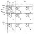
또한, 개시하는 발명의 다른 실시 형태에 따르면, 반도체 장치는 복수의 비트선과, 복수의 소스선과, 복수의 기입 워드선과, 복수의 기입-판독 워드선과, 복수의 메모리 셀을 포함하는 메모리 셀 어레이를 포함한다. 각 메모리 셀은 제1 게이트 전극, 제1 소스 영역, 제1 드레인 영역, 및 제1 채널 형성 영역을 포함하는 제1 트랜지스터와; 제2 게이트 전극, 제2 소스 전극, 제2 드레인 전극, 및 적어도 제1 소스 영역 또는 제1 드레인 영역의 일부와 중첩하도록 설치된 제2 채널 형성 영역을 포함하는 제2 트랜지스터와; 용량 소자를 포함한다. 소스선은 제1 소스 영역과 전기적으로 접속된다. 비트선은 제1 드레인 영역 및 제2 소스 전극과 전기적으로 접속된다. 기입-판독 워드선은 용량 소자의 한쪽의 전극과 전기적으로 접속된다. 기입 워드선은 제2 게이트 전극과 전기적으로 접속된다. 제1 게이트 전극과, 제2 드레인 전극과, 용량 소자의 다른 쪽 전극은 서로 전기적으로 접속되어서 전하가 유지되는 노드를 구성한다. 메모리 셀의 기입 기간에 있어서, 적어도 복수의 비트선에 정의 전위가 부여될 때에, 선택 행에 있는 복수의 기입 워드선 중 하나에 정의 전위가 부여되고, 비선택 행에 있는 복수의 기입 워드선 중 다른 하나에 부의 전위가 부여된다. 메모리 셀의 판독 기간에 있어서, 적어도 복수의 비트선에 정의 전위가 부여될 때에, 복수의 기입 워드선에 부의 전위가 부여된다.According to another embodiment of the disclosed invention, a semiconductor device includes a memory cell array including a plurality of bit lines, a plurality of source lines, a plurality of write word lines, a plurality of write-read word lines, and a plurality of memory cells . Each memory cell comprising: a first transistor including a first gate electrode, a first source region, a first drain region, and a first channel formation region; A second transistor including a second gate electrode, a second source electrode, a second drain electrode, and a second channel formation region provided so as to overlap at least a portion of the first source region or the first drain region; And a capacitive element. The source line is electrically connected to the first source region. The bit line is electrically connected to the first drain region and the second source electrode. The write-read word line is electrically connected to one electrode of the capacitive element. The write word line is electrically connected to the second gate electrode. The first gate electrode, the second drain electrode, and the other electrode of the capacitor element are electrically connected to each other to constitute a node where charge is held. When a positive potential is applied to at least a plurality of bit lines in a write period of a memory cell, a positive potential is given to one of a plurality of write word lines in a selected row, and a positive potential is applied to one of a plurality of write word lines And a negative potential is imparted to the other one. When a positive potential is applied to at least a plurality of bit lines in a read period of a memory cell, a negative potential is applied to a plurality of write word lines.
또한, 제1 채널 형성 영역과 제2 채널 형성 영역은 다른 반도체 재료를 포함하는 것이 바람직하다. 또한, 제2 채널 형성 영역은 산화물 반도체를 포함하는 것이 바람직하다.Further, it is preferable that the first channel forming region and the second channel forming region include different semiconductor materials. Further, it is preferable that the second channel formation region includes an oxide semiconductor.
상기 반도체 장치에서는 산화물 반도체 재료를 사용해서 트랜지스터를 구성하고 있지만, 본 발명의 한 실시 형태는 산화물 반도체 재료를 사용하는 것에 한정되지 않는다는 점에 주목한다. 산화물 반도체 재료와 동등한 오프 전류 특성을 실현할 수 있는 재료, 예를 들어, 탄화 실리콘을 비롯한 와이드 갭 재료(구체적으로는, 에너지 갭 Eg이 3eV보다 큰 반도체 재료) 등을 사용해도 된다.Although the above semiconductor device uses the oxide semiconductor material to construct the transistor, it is noted that one embodiment of the present invention is not limited to the use of the oxide semiconductor material. For example, a wide gap material (specifically, a semiconductor material having an energy gap Eg of greater than 3 eV) including silicon carbide, or the like, which can realize an off current characteristic equivalent to that of an oxide semiconductor material.
본 명세서 등에 있어서 "위"나 "아래" 등의 용어는, 구성 요소의 위치 관계가 반드시 "바로 위" 또는 "바로 아래"인 것을 한정하는 것이 아니라는 점에 주목한다. 예를 들어, "게이트 절연층 위의 게이트 전극"이란 표현이면, 게이트 절연층과 게이트 전극 사이에 다른 구성 요소를 포함하는 것을 배제하지 않는다.It is noted that the terms "above" or "below " in this specification and the like do not limit that the positional relationship of the components is necessarily" directly above "or" directly below ". For example, the expression "gate electrode on the gate insulating layer" does not exclude the inclusion of other components between the gate insulating layer and the gate electrode.
또한, 본 명세서 등에 있어서 "전극"이나 "배선"이라고 하는 용어는 이들 구성 요소를 기능적으로 한정하는 것이 아니다. 예를 들어, " 전극"은 " 배선"의 일부로서 사용되는 경우가 있고, 그의 반대도 또한 마찬가지이다. 또한, "전극"이나 "배선"이라고 하는 용어는, 복수의 "전극"이나 "배선"이 일체로 되어 형성되어 있는 경우 등도 포함한다.Note that the term "electrode" or "wiring" in this specification does not functionally limit these constituent elements. For example, "electrode" may be used as part of "wiring ", and vice versa. The term "electrode" or "wiring" includes the case where a plurality of "electrodes" and "wiring"
"소스" 및 "드레인"의 기능은 상이한 극성의 트랜지스터를 채용하는 경우나, 회로 동작에 있어서 전류의 방향이 변화하는 경우 등에는 서로 바뀔 때도 있다. 이로 인해, 본 명세서에 있어서는, "소스" 및 "드레인"의 용어는 각각 드레인이나 소스를지칭하는데 사용할 수 있다.The functions of "source" and "drain" may be mutually changed when transistors of different polarities are employed, or when the direction of the current changes in the circuit operation. For this reason, in this specification, the terms "source" and "drain" may be used to refer to a drain or a source, respectively.
본 명세서 등에 있어서, "전기적으로 접속"에는, 구성요소가 어떠한 전기적 작용을 갖는 물체를 개재해서 접속되어 있는 경우가 포함된다는 점에 주목한다. 여기서, 어떠한 전기적 작용을 갖는 물체는 접속 대상 간에서의 전기 신호의 수수를 가능하게 하는 것이면, 특별히 제한을 받지 않는다.Note that, in this specification and the like, "electrically connecting" includes the case where the components are connected via an object having any electrical action. Here, any object having any electrical action is not particularly limited as long as it enables the transmission of electric signals between connection objects.
예를 들어, "어떠한 전기적 작용을 갖는 물체"에는, 전극이나 배선을 비롯하여, 트랜지스터 등의 스위칭 소자, 저항 소자, 인덕터, 캐패시터, 및 각종 기능을 갖는 소자 등이 포함된다.For example, "an object having any electrical action" includes an electrode, a wiring, a switching element such as a transistor, a resistance element, an inductor, a capacitor, and an element having various functions.
산화물 반도체를 포함하는 트랜지스터는 오프 전류가 극히 작기 때문에, 이트랜지스터를 사용함으로써 극히 장기간에 걸쳐 기억된 데이터를 유지하는 것이 가능하다. 즉, 리프레시 동작이 불필요하게 되거나 또는 리프레시 동작의 빈도를 극히 낮게 하는 것이 가능하게 되기 때문에, 소비 전력을 충분히 저감할 수 있다. 또한, 전력의 공급이 중단되는 경우에도, 장기간에 걸쳐서 기억된 데이터를 유지하는 것이 가능하다.Since the transistor including the oxide semiconductor has an extremely small off current, it is possible to maintain the data stored over an extremely long period of time by using this transistor. That is, since the refresh operation becomes unnecessary or the frequency of the refresh operation can be made extremely low, the power consumption can be sufficiently reduced. Further, even when the supply of electric power is interrupted, it is possible to retain the stored data for a long period of time.
또한, 본 발명의 한 실시 형태에 따른 반도체 장치에서는, 데이터의 기입에 높은 전압을 필요로 하지 않고, 소자의 열화의 문제도 없다. 예를 들어, 종래의 불휘발성 메모리와 같이, 부유 게이트에의 전자의 주입이나, 부유 게이트로부터의 전자의 추출을 행할 필요가 없기 때문에, 게이트 절연층의 열화 문제가 발생하지 않는다. 즉, 본 발명의 한 실시 형태에 따른 반도체 장치에서는, 종래의 불휘발성 메모리에서 문제가 되고 있는 재기입 가능 횟수에 제한이 없고, 그 신뢰성이 비약적으로 향상한다. 또한, 트랜지스터의 온 상태 또는 오프 상태에 따라, 데이터의 기입이 행해지기 때문에, 고속의 동작도 용이하게 실현할 수 있다. 또한, 데이터를 소거하기 위한 동작이 불필요하다고 하는 장점도 있다.Further, in the semiconductor device according to the embodiment of the present invention, a high voltage is not required for data writing, and there is no problem of deterioration of the device. For example, since there is no need to inject electrons into the floating gate or extract electrons from the floating gate as in the conventional nonvolatile memory, the problem of deterioration of the gate insulating layer does not occur. That is, in the semiconductor device according to the embodiment of the present invention, there is no limitation on the number of rewritable times which is a problem in the conventional nonvolatile memory, and the reliability thereof is remarkably improved. In addition, because data is written in accordance with the ON or OFF state of the transistor, high-speed operation can be easily realized. There is also an advantage that an operation for erasing data is unnecessary.
산화물 반도체 이외의 재료를 포함하는 트랜지스터는 충분한 고속 동작이 가능하기 때문에, 산화물 반도체를 포함하는 트랜지스터와 조합해서 사용함으로써, 반도체 장치의 동작(예를 들어, 데이터의 판독)의 고속성을 충분히 확보할 수 있다. 또한, 산화물 반도체 이외의 재료를 포함하는 트랜지스터에 의해, 고속 동작이 요구되는 각종 회로(논리 회로 또는 구동 회로 등)를 양호하게 실현하는 것이 가능하다.Since a transistor including a material other than an oxide semiconductor can perform a sufficiently high-speed operation, by using it in combination with a transistor including an oxide semiconductor, it is possible to sufficiently secure the high quality of the operation (for example, reading of data) . In addition, it is possible to satisfactorily realize various circuits (such as a logic circuit or a drive circuit) that require high-speed operation by a transistor including a material other than an oxide semiconductor.
또한, 산화물 반도체 이외의 재료를 사용한 트랜지스터와 산화물 반도체를 사용한 트랜지스터는 적어도 일부가 서로 중첩하고, 특히, 산화물 반도체 이외의 재료를 사용한 트랜지스터의 소스 영역 또는 드레인 영역과 산화물 반도체층의 일부가 서로 중첩하도록 설치되어 있으므로, 반도체 장치의 고집적화를 도모할 수 있다. 또한, 산화물 반도체 이외의 재료를 사용한 트랜지스터를 오프 상태로 해야 할 기간에 있어서, 적어도 산화물 반도체를 사용한 트랜지스터의 소스 영역 또는 드레인 영역에 정의 전위를 부여할 때에 산화물 반도체 이외의 재료를 사용한 트랜지스터의 게이트 전극에 부의 전위를 부여하는 것에 의해, 반도체 장치의 메모리 리텐션(retention) 특성을 향상시킬 수 있다.In addition, a transistor using a material other than an oxide semiconductor and a transistor using an oxide semiconductor are at least partially overlapped with each other. Particularly, a source region or a drain region of a transistor using a material other than the oxide semiconductor and a part of the oxide semiconductor layer overlap each other So that the semiconductor device can be highly integrated. When a positive potential is applied to at least a source region or a drain region of a transistor using an oxide semiconductor in a period in which a transistor using a material other than the oxide semiconductor is to be turned off, It is possible to improve the memory retention characteristic of the semiconductor device.
산화물 반도체 이외의 재료를 포함하는 트랜지스터(보다 광의로는, 충분한 고속 동작이 가능한 트랜지스터)와 산화물 반도체를 포함하는 트랜지스터(보다 광의로는, 충분히 오프 전류가 작은 트랜지스터)를 일체로 구비함으로써 신규한 특징을 갖는 반도체 장치를 실현할 수 있다.A transistor including a material other than an oxide semiconductor (a transistor capable of performing a sufficiently high-speed operation in a broader sense) and a transistor including an oxide semiconductor (a transistor having a sufficiently small off-current in a broader sense) Can be realized.
도 1a 및 1b는 반도체 장치의 단면도 및 평면도.
도 2a 및 2b는 반도체 장치의 단면도 및 평면도.
도 3a 내지 3d는 반도체 장치의 회로도.
도 4는 반도체 장치의 회로도.
도 5는 반도체 장치의 타이밍 차트.
도 6은 반도체 장치의 타이밍 차트.
도 7의 (a) 내지 (g)는 반도체 장치의 제작 공정을 도시하는 단면도.
도 8의 (a) 내지 (e)는 반도체 장치의 제작 공정을 도시하는 단면도.
도 9의 (a) 내지 (d)는 반도체 장치의 제작 공정을 도시하는 단면도.
도 10의 (a) 내지 (d)는 반도체 장치의 제작 공정을 도시하는 단면도.
도 11의 (a) 내지 (c)는 반도체 장치의 제작 공정을 도시하는 단면도.
도 12a 및 12b는 반도체 장치의 단면도.
도 13a 내지 도 13c는 반도체 장치의 제작 공정을 도시하는 단면도.
도 14a 내지 14f는 반도체 장치를 사용한 전자 기기를 설명하기 위한 도면.
도 15a 내지 15e는 본 발명의 한 실시 형태에 따른 산화물 재료의 구조를 설명하는 도면.
도 16의 (a) 내지 (c)는 본 발명의 한 실시 형태에 따른 산화물 재료의 구조를 설명하는 도면.
도 17의 (a) 내지 (c)는 본 발명의 한 실시 형태에 따른 산화물 재료의 구조를 설명하는 도면.
도 18은 계산에 의해 얻어진 이동도의 게이트 전압 의존성을 설명하는 도면.
도 19a 내지 19c는 계산에 의해 얻어진 드레인 전류와 이동도의 게이트 전압 의존성을 설명하는 도면.
도 20a 내지 20c는 계산에 의해 얻어진 드레인 전류와 이동도의 게이트 전압 의존성을 설명하는 도면.
도 21a 내지 21c는 계산에 의해 얻어진 드레인 전류와 이동도의 게이트 전압 의존성을 설명하는 도면.
도 22a 및 22b는 계산에 사용한 트랜지스터의 단면 구조를 설명하는 도면.
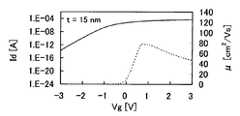
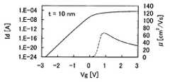
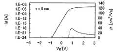
도 23a 내지 23c는 본 발명의 한 실시 형태에 따른 트랜지스터의 특성을 도시하는 도면.
도 24a 및 24b는 본 발명의 한 실시 형태에 따른 트랜지스터의 특성을 도시하는 도면.
도 25a 및 25b는 본 발명의 한 실시 형태에 따른 트랜지스터의 특성을 도시하는 도면.
도 26은 본 발명의 한 실시 형태에 따른 트랜지스터의 특성을 도시하는 도면.
도 27a 및 27b는 본 발명의 한 실시 형태에 따른 트랜지스터의 특성을 도시하는 도면.
도 28은 본 발명의 한 실시 형태에 따른 트랜지스터의 XRD 스펙트럼을 도시하는 그래프.
도 29는 본 발명의 한 실시 형태에 따른 트랜지스터의 특성을 도시하는 그래프.
도 30a 및 30b는 본 발명의 한 실시 형태에 따른 트랜지스터의 구조를 설명하는 도면.
도 31a 및 31b는 본 발명의 한 실시 형태에 따른 트랜지스터의 구조를 설명하는 도면.
도 32a 및 도 32b는 본 발명의 한 실시 형태에 따른 산화물 재료의 구조를 설명하는 도면.1A and 1B are a cross-sectional view and a plan view of a semiconductor device;
2A and 2B are a cross-sectional view and a plan view of a semiconductor device;
3A to 3D are circuit diagrams of a semiconductor device.
4 is a circuit diagram of a semiconductor device.
5 is a timing chart of a semiconductor device.
6 is a timing chart of the semiconductor device.
7 (a) to 7 (g) are cross-sectional views showing steps of manufacturing a semiconductor device.
8 (a) to 8 (e) are cross-sectional views showing a manufacturing process of a semiconductor device.
9 (a) to 9 (d) are sectional views showing steps of manufacturing a semiconductor device.
10 (a) to 10 (d) are cross-sectional views showing steps of manufacturing a semiconductor device.
11 (a) to 11 (c) are cross-sectional views showing steps of manufacturing a semiconductor device.
12A and 12B are cross-sectional views of a semiconductor device;
13A to 13C are cross-sectional views showing a manufacturing process of a semiconductor device.
14A to 14F are diagrams for explaining an electronic apparatus using a semiconductor device.
15A to 15E are diagrams illustrating the structure of an oxide material according to one embodiment of the present invention.
16A to 16C are diagrams for explaining the structure of an oxide material according to one embodiment of the present invention.
17 (a) to 17 (c) are diagrams for explaining the structure of an oxide material according to one embodiment of the present invention.
18 is a view for explaining the gate voltage dependency of mobility obtained by calculation;
19A to 19C are diagrams for explaining the gate voltage dependency of the drain current and the mobility obtained by calculation;
20A to 20C are diagrams for explaining the drain current and gate voltage dependence of mobility obtained by calculation;
21A to 21C are diagrams for explaining the gate voltage dependency of the drain current and the mobility obtained by calculation;
22A and 22B are diagrams for explaining a cross-sectional structure of a transistor used for calculation;
23A to 23C are diagrams showing the characteristics of a transistor according to an embodiment of the present invention.
24A and 24B are diagrams showing the characteristics of a transistor according to an embodiment of the present invention.
25A and 25B are diagrams showing the characteristics of a transistor according to an embodiment of the present invention.
26 is a diagram showing the characteristics of a transistor according to an embodiment of the present invention;
27A and 27B are diagrams showing the characteristics of a transistor according to an embodiment of the present invention.
28 is a graph showing an XRD spectrum of a transistor according to an embodiment of the present invention.
29 is a graph showing the characteristics of a transistor according to one embodiment of the present invention.
30A and 30B are diagrams for explaining the structure of a transistor according to an embodiment of the present invention;
31A and 31B are diagrams for explaining the structure of a transistor according to one embodiment of the present invention.
32A and 32B are diagrams illustrating the structure of an oxide material according to one embodiment of the present invention.
본 발명의 실시 형태 및 일례에 대해서, 도면을 사용해서 이하에 설명한다. 본 발명은 이하의 설명에 한정되지 않고, 본 발명의 취지 및 그 범위로부터 벗어나지 않고 그 형태 및 상세를 다양하게 변경할 수 있는 것은 당업자라면 용이하게 이해된다는 점에 주목한다. 따라서, 본 발명은 다음의 실시 형태 및 일례의 기재 내용에 한정해서 해석되지 않는다.Embodiments and examples of the present invention will be described below with reference to the drawings. It is to be noted that the present invention is not limited to the following description, and it is easily understood by those skilled in the art that various changes can be made in form and details without departing from the spirit and scope of the present invention. Therefore, the present invention is not construed as being limited to the description of the following embodiments and examples.
도면 등에 있어서 나타내는 각 구성의 위치, 크기, 범위 등은 이해의 간단화를 위하여, 실제의 위치, 크기, 범위 등을 나타내고 있지 않은 경우가 있다는 점에 주목한다. 이로 인해, 본 발명의 한 실시 형태는 반드시 도면 등에 도시된 위치, 크기, 범위 등에 한정되지 않는다.Note that the position, size, range, and the like of each configuration shown in the drawings and the like may not represent the actual position, size, range, and the like in order to simplify the understanding. For this reason, one embodiment of the present invention is not necessarily limited to the position, size, range, etc. shown in the drawings and the like.
본 명세서 등에 있어서의 "제1", "제2", 및 "제3" 등의 서수는, 구성 요소의 혼동을 피하기 위해서 사용된 것이며, 구성 요소를 수적으로 한정하는 것은 아니다.The ordinal numbers such as " first ", "second ", and" third "in the present specification are used for avoiding confusion of components and are not intended to limit the components numerically.
(실시 형태 1)(Embodiment 1)
본 실시 형태에서는, 본 발명의 한 실시 형태에 따른 반도체 장치의 구성 및 구동 방법에 대해서, 도 1a 및 1b, 도 2a 및 2b, 도 3a 내지 3d, 도 4, 도 5, 및 도 6을 참조하여 설명한다.In the present embodiment, the configuration and the driving method of the semiconductor device according to one embodiment of the present invention will be described with reference to Figs. 1A and 1B, 2A and 2B, 3A to 3D, 4, Explain.
< 반도체 장치의 단면 구성 및 평면도><Sectional Configuration and Plan of Semiconductor Device>
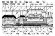
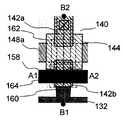
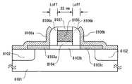
도 1a 및 1b는 반도체 장치의 구성의 일례이다. 도 1a는 반도체 장치의 단면도이다. 도 1b는 반도체 장치의 평면도이다. 도 1a는 트랜지스터의 채널 길이 방향에 수직한 단면도이며, 도 1b는 트랜지스터의 채널 길이 방향에 평행한 단면도이다. 도 1a 및 1b에 도시하는 반도체 장치는 하부에 제1 반도체 재료를 포함하는 트랜지스터(160)와, 상부에 제2 반도체 재료를 포함하는 트랜지스터(162)를 포함한다. 도 1a 및 1b에 도시하는 반도체 장치는 트랜지스터(160)와, 트랜지스터(162)와, 용량 소자(164)를 하나씩 포함하는 구성으로서 나타내고 있지만, 이 반도체 장치는 복수의 트랜지스터(160)와, 트랜지스터(162)와, 용량 소자(164)를 포함할 수 있다.1A and 1B are an example of a configuration of a semiconductor device. 1A is a cross-sectional view of a semiconductor device. 1B is a plan view of the semiconductor device. 1A is a cross-sectional view perpendicular to a channel length direction of a transistor, and FIG. 1B is a cross-sectional view parallel to a channel length direction of a transistor. The semiconductor device shown in Figs. 1A and 1B includes a
여기서, 제1 반도체 재료와 제2 반도체 재료는 상이한 재료로 하는 것이 바람직하다. 예를 들어, 제1 반도체 재료로서 산화물 반도체 이외의 반도체 재료를 사용할 수 있고, 제2 반도체 재료로서 산화물 반도체를 사용할 수 있다. 산화물 반도체 이외의 반도체 재료로서는, 예를 들어, 실리콘, 게르마늄, 실리콘 게르마늄, 탄화 실리콘, 갈륨 비소 등을 사용할 수 있고, 단결정 반도체를 사용하는 것이 바람직하다. 이외에, 유기 반도체 재료 등을 사용해도 된다. 이러한 반도체 재료를 포함하는 트랜지스터는 고속 동작이 용이하다. 한편, 산화물 반도체를 포함하는 트랜지스터는 그 특성에 의해 장기간의 전하 유지를 가능하게 한다.Here, it is preferable that the first semiconductor material and the second semiconductor material are made of different materials. For example, a semiconductor material other than an oxide semiconductor may be used as the first semiconductor material, and an oxide semiconductor may be used as the second semiconductor material. As the semiconductor material other than the oxide semiconductor, for example, silicon, germanium, silicon germanium, silicon carbide, gallium arsenide and the like can be used, and a single crystal semiconductor is preferably used. In addition, an organic semiconductor material or the like may be used. A transistor including such a semiconductor material is easy to operate at high speed. On the other hand, a transistor including an oxide semiconductor enables long-term charge retention by its characteristics.
사용하는 산화물 반도체로서는, 적어도 인듐(In) 또는 아연(Zn)을 포함하는 것이 바람직하다. 특히, In과 Zn을 포함하는 것이 바람직하다. 상기 산화물 반도체를 사용한 트랜지스터의 전기 특성의 변동을 저감시키기 위한 스테빌라이저(stabilizer)로서, 갈륨(Ga)을 부가적으로 함유하는 것이 바람직하다. 스테빌라이저로서 주석(Sn)을 함유하는 것이 바람직하다. 스테빌라이저로서 하프늄(Hf)을 함유하는 것이 바람직하다. 스테빌라이저로서 알루미늄(Al)을 함유하는 것이 바람직하다.As the oxide semiconductor to be used, it is preferable to include at least indium (In) or zinc (Zn). In particular, it is preferable to include In and Zn. As the stabilizer for reducing fluctuation of the electric characteristics of the transistor using the oxide semiconductor, it is preferable to additionally contain gallium (Ga). It is preferable that tin (Sn) is contained as a stabilizer. It is preferable that hafnium (Hf) is contained as a stabilizer. It is preferable that aluminum (Al) is contained as a stabilizer.
또한, 다른 스테빌라이저(들)로서, 란타노이드인 란탄(La), 세륨(Ce), 프라세오디뮴(Pr), 네오디뮴(Nd), 사마륨(Sm), 유로퓸(Eu), 가돌리늄(Gd), 테르븀(Tb), 디스프로슘(Dy), 홀뮴(Ho), 에르븀(Er), 툴륨(Tm), 이테르븀(Yb), 또는 루테튬(Lu) 중 하나 이상을 함유할 수 있다.As another stabilizer (s), lanthanides La, Ce, Pr, Ne, Sm, Eu, Gd, Terbium, Tb, Dys, Ho, Er, Tm, Yb, or Lu.
예를 들어, 산화물 반도체로서, 산화 인듐, 산화 주석, 산화 아연, 2원계 금속의 산화물인 In-Zn계 산화물, Sn-Zn계 산화물, Al-Zn계 산화물, Zn-Mg계 산화물, Sn-Mg계 산화물, In-Mg계 산화물, 또는 In-Ga계 산화물, 3원계 금속의 산화물인 In-Ga-Zn계 산화물(IGZO라고도 표기한다), In-Al-Zn계 산화물, In-Sn-Zn계 산화물, Sn-Ga-Zn계 산화물, Al-Ga-Zn계 산화물, Sn-Al-Zn계 산화물, In-Hf-Zn계 산화물, In-La-Zn계 산화물, In-Ce-Zn계 산화물, In-Pr-Zn계 산화물, In-Nd-Zn계 산화물, In-Sm-Zn계 산화물, In-Eu-Zn계 산화물, In-Gd-Zn계 산화물, In-Tb-Zn계 산화물, In-Dy-Zn계 산화물, In-Ho-Zn계 산화물, In-Er-Zn계 산화물, In-Tm-Zn계 산화물, In-Yb-Zn계 산화물, 또는 In-Lu-Zn계 산화물, 4원계 금속의 산화물인 In-Sn-Ga-Zn계 산화물, In-Hf-Ga-Zn계 산화물, In-Al-Ga-Zn계 산화물, In-Sn-Al-Zn계 산화물, In-Sn-Hf-Zn계 산화물, 또는 In-Hf-Al-Zn계 산화물을 사용할 수 있다.Examples of the oxide semiconductor include indium oxide, tin oxide, zinc oxide, an In-Zn-based oxide, an Sn-Zn-based oxide, an Al-Zn-based oxide, a Zn-Mg- In-Ga-Zn oxide (also referred to as IGZO), an In-Al-Zn oxide, an In-Sn-Zn oxide Zn-based oxide, In-Ce-Zn-based oxide, Sn-Ga-Zn-based oxide, Al-Ga-Zn-based oxide, Sn-Al- In-Zn-based oxide, In-Tb-Zn-based oxide, In-Nd-Zn-based oxide, In-Sm-Zn-based oxide, In- In-Zn-based oxide, In-Er-Zn-based oxide, In-Tm-Zn-based oxide, In-Yb-Zn- In-Sn-Zn-Zn oxide, In-Sn-Zn-Zn oxide, In-Sn-Zn-Zn oxide, Based oxide, or In-Hf-Al-Zn-based acid Cargo can be used.
여기에서, 예를 들어, "In-Ga-Zn-O계 산화물"이란 In, Ga, 및 Zn을 주성분으로서 함유하는 산화물을 의미하며 In: Ga: Zn의 비율은 특정하게 한정되지 않는다는 점에 주목한다. 또한, In, Ga, 및 Zn 이외의 금속 원소가 함유될 수 있다.Herein, for example, "In-Ga-Zn-O-based oxide" means an oxide containing In, Ga, and Zn as main components, and it is noted that the ratio of In: Ga: Zn is not particularly limited do. In addition, metal elements other than In, Ga, and Zn may be contained.
또한, 산화물 반도체로서, InMO3(ZnO)m (m> 0, 또한, m은 정수가 아니다)로 표기되는 재료를 사용해도 된다. M은 Ga, Fe, Mn 및 Co로부터 선택된 하나 이상의 금속 원소를 나타낸다는 점에 주목한다. 또한, 산화물 반도체로서, In3SnO5(ZnO)n(n> 0, 또한, n은 정수)로 표기되는 재료를 사용해도 된다.As the oxide semiconductor, a material represented by InMO3 (ZnO)m (m> 0, and m is not an integer) may be used. Note that M represents at least one metal element selected from Ga, Fe, Mn and Co. As the oxide semiconductor, a material expressed by In3 SnO5 (ZnO)n (n> 0, and n is an integer) may be used.
산화물 반도체로서 In-Ga-Zn계 산화물 반도체막을 스퍼터링법으로 성막하는 경우에, 바람직하게는 원자수비가 In:Ga:Zn=1:1:1, 4:2:3, 3:1:2, 1:1:2, 2:1:3, 또는 3:1:4로 나타나는 In-Ga-Zn계 산화물 타깃을 사용한다. 전술한 원자수비를 갖는 In-Ga-Zn계 산화물 타깃을 사용해서 산화물 반도체를 성막할 때, 다결정 또는 후술하는 c축 배향 결정(CAAC)이 형성되기 쉬워진다.When an In-Ga-Zn-based oxide semiconductor film is formed as an oxide semiconductor by the sputtering method, the atomic ratio is preferably in the range of In: Ga: Zn = 1: 1: 1, 4: 2: 3, 3: In-Ga-Zn-based oxide targets represented by 1: 1: 2, 2: 1: 3, or 3: 1: 4 are used. When an oxide semiconductor is formed using an In-Ga-Zn-based oxide target having the above-described atomic ratio, a polycrystal or a c-axis oriented crystal (CAAC) described later tends to be easily formed.
산화물 반도체로서 In-Sn-Zn계 산화물을 스퍼터링법으로 성막하는 경우에, 바람직하게는 원자수비가 In:Sn:Zn=1:1:1, 2:1:3, 1:2:2, 또는 20:45:35로 나타나는 In-Sn-Zn계 산화물 타깃을 사용한다. 전술한 원자수비를 갖는 In-Sn-Zn계 산화물 타깃을 사용해서 산화물 반도체를 성막할 때, 다결정 또는 후술하는 CAAC이 형성되기 쉬워진다.When the In-Sn-Zn-based oxide is formed as an oxide semiconductor by the sputtering method, the atomic ratio is preferably 1: 1: 1, 2: 1: 3, 1: 2: 2, In-Sn-Zn-based oxide target represented by 20:45:35 is used. When an oxide semiconductor is formed using an In-Sn-Zn-based oxide target having the above-described atomic ratio, a polycrystal or a CAAC described below is likely to be formed.
그러나, 조성은 상술한 것들에 한정되지 않고, 필요로 하는 반도체 특성(예를 들어, 이동도, 임계값, 및 변동)에 따라서 적절한 조성의 재료를 사용하면 된다. 필요로 하는 반도체 특성을 얻기 위해서, 캐리어 농도, 불순물 농도, 결함 밀도, 금속 원소와 산소의 원자수비, 원자간 결합 거리, 밀도 등을 적절한 것으로 설정하는 것이 바람직하다.However, the composition is not limited to those described above, and a material having an appropriate composition may be used according to the required semiconductor characteristics (for example, mobility, threshold, and variation). It is preferable to set the carrier concentration, the impurity concentration, the defect density, the atomic number ratio of the metal element and oxygen, the distance between the atoms and the bond, and the density to be appropriate in order to obtain the required semiconductor characteristics.
예를 들어, In-Sn-Zn계 산화물에서는, 비교적 용이하게 높은 이동도가 얻어질 수 있다. 그러나, In-Ga-Zn계 산화물을 사용하는 경우도, 벌크 내 결함 밀도를 저감함으로써 이동도를 올릴 수 있다.For example, in an In-Sn-Zn based oxide, a relatively high mobility can be obtained easily. However, even when the In-Ga-Zn-based oxide is used, the mobility can be increased by reducing the defect density in the bulk.
예를 들어 "In, Ga, 및 Zn의 원자수비가 In:Ga:Zn=a:b:c (a+b+c=1)인 산화물의 조성이, In, Ga, 및 Zn의 원자수비가 In:Ga:Zn=A:B:C (A+B+C=1)의 산화물의 조성의 근방이다"라고 하는 것은 a, b, 및 c가 (a-A)2+(b-B)2+(c-C)2≤r2를 만족하는 것을 의미하고, r로서는, 예를 들어, 0.05로 하면 된다는 점에 주목한다. 다른 산화물에서도 마찬가지이다.For example, when the composition of an oxide in which the atomic ratio of In, Ga and Zn is In: Ga: Zn = a: b: c (a + b + c = 1) (AA)2 + (bB)2 + (cC) where a, b, and c satisfy the following relationship: )2? R2, and it is to be noted that r may be 0.05, for example. The same is true for other oxides.
산화물 반도체는 단결정이어도 되고, 비단결정이어도 된다. 후자의 경우, 산화물 반도체는 아몰퍼스이어도 되고, 다결정이어도 된다. 또한, 산화물 반도체는 아몰퍼스 중에 결정성을 갖는 부분을 포함하는 구조도 되고, 비아몰퍼스 구조이어도 된다.The oxide semiconductor may be a single crystal or a non-crystal. In the latter case, the oxide semiconductor may be amorphous or polycrystalline. The oxide semiconductor may have a structure including a portion having crystallinity in the amorphous structure or a non-amorphous structure.
아몰퍼스 상태의 산화물 반도체에서는, 비교적 용이하게 평탄한 표면을 얻을 수 있기 때문에, 이 산화물 반도체를 사용해서 트랜지스터를 제작할 때, 계면 산란을 저감할 수 있고, 비교적 용이하게, 비교적 높은 이동도를 얻을 수 있다.In amorphous oxide semiconductors, a comparatively easily smooth surface can be obtained. Therefore, when a transistor is fabricated using this oxide semiconductor, interface scattering can be reduced, and comparatively high mobility can be obtained relatively easily.
결정성을 갖는 산화물 반도체에서는, 벌크 내 결함을 더 저감할 수 있고, 표면의 평탄성을 높이면, 아몰퍼스 상태의 산화물 반도체 이상의 이동도를 얻을 수 있다. 표면의 평탄성을 높이기 위해서는, 평탄한 표면 위에 산화물 반도체를 형성하는 것이 바람직하다. 구체적으로는, 평균면 거칠기(Ra)가 1nm 이하, 바람직하게는 0.3nm 이하, 보다 바람직하게는 0.1nm 이하의 표면 위에 산화물 반도체를 형성하면 된다.In the oxide semiconductor having crystallinity, defects in the bulk can be further reduced, and mobility higher than that of the amorphous oxide semiconductor can be obtained by increasing the flatness of the surface. In order to increase the flatness of the surface, it is preferable to form an oxide semiconductor on a flat surface. Specifically, the average surface roughness (Ra) is, more preferably 1nm or less, preferably 0.3nm or less may be formed on the surface of an oxide semiconductor less than 0.1nm.
평균면 거칠기(Ra)는 JIS B 0601로 정의되어 있는 중심선 평균 거칠기를 측정 면에 대하여 적용할 수 있도록 삼차원으로 확장한 것이라는 점에 주목한다. Ra는 "기준면으로부터 지정면까지의 편차의 절대값을 평균한 값"이라고 표현할 수 있고, 이하의 수학식으로 정의된다.Note that the average surface roughness (Ra ) isa three-dimensional extension of the center line average roughness defined in JIS B 0601 so that it can be applied to the measurement surface. Ra can be expressed as "a value obtained by averaging the absolute values of the deviations from the reference surface to the designated surface ", and is defined by the following equation.

상기 수학식에 있어서, S0은 측정면(좌표(x1,y1),(x1,y2),(x2,y1),및 (x2,y2)로 표현되는 4점에 의해 정해지는 직사각형의 영역)의 면적을 나타내고, Z0은 측정면의 평균 높이를 나타낸다. Ra는 원자간력 현미경(AFM)을 사용하여 측정가능하다.In the above equation, S0 is the measuring surface (coordinate(x 1, y 1), 4 points, represented by(x 1, y 2), (x 2, y 1), and (x2, y2) , And Z0 represents the average height of the measurement surface. Ra can be measured using an atomic force microscope (AFM).
여기서, 산화물 반도체가 결정성을 갖는 경우에는, c축 배향하고, 또한 ab면, 표면 또는 계면의 방향으로부터 보아서 삼각형 또는 육각형의 원자 배열을 갖는 결정(C-Axis Aligned Crystal(CAAC)이라고도 한다)을 포함하는 산화물에 대해서 설명한다. 결정에 있어서, c축을 따라서 금속 원자가 층상 또는 금속 원자와 산소 원자가 층상으로 배열되어 있고, ab면에 있어서는 a축 또는 b축의 방향이 다르다(결정이 c축을 중심으로 회전).Here, when the oxide semiconductor has crystallinity, crystals (also referred to as C-Axis Aligned Crystal (CAAC)) having a c-axis orientation and a triangular or hexagonal atomic arrangement as viewed from the ab plane, The oxides that will be included are described below. In the crystal, metal atoms are arranged in layers on the c-axis, or metal atoms and oxygen atoms are arranged in layers on the c-axis, and the directions of the a-axis or b-axis are different on the ab-plane (crystals are rotated around the c-axis).
광의로는, CAAC을 포함하는 산화물은 비단결정이며, 그 ab면에 수직인 방향으로부터 보아서, 삼각형, 육각형, 정삼각형, 또는 정육각형의 원자 배열을 갖고, 또한 c축 방향에 수직인 방향으로부터 보아서, 금속 원자가 층상 또는 금속 원자와 산소 원자가 층상으로 배열된 상을 포함하는 산화물을 말한다.As a matter of fact, the oxide containing CAAC is non-crystalline and has an atomic arrangement of triangular, hexagonal, regular triangular, or regular hexagonal shape when viewed from the direction perpendicular to the ab plane, Atomic layer refers to an oxide containing a layer or a phase in which metal atoms and oxygen atoms are arranged in layers.
CAAC은 단결정이 아니지만, CAAC가 비정질 성분만으로 형성되어 있는 것을 의미하지는 않는다. CAAC은 결정화한 부분(결정 부분)을 포함하지만, 1개의 결정 부분과 다른 결정 부분 간의 경계를 명확하게 판별 가능하지 않은 경우도 있다.CAAC is not a single crystal, but it does not mean that CAAC is formed of only amorphous components. The CAAC includes a crystallized part (crystal part), but there is also a case where the boundary between one crystal part and another crystal part can not be clearly discriminated.
CAAC에 산소가 포함되는 경우에, CAAC에 포함되는 산소의 일부는 질소로 치환될 수 있다. CAAC에 포함되는 개개의 결정 부분의 c축은 일정한 방향(예를 들어, CAAC가 형성되는 기판면 또는 CAAC의 표면에 수직인 방향)에 정렬될 수 있다. 또는, CAAC에 포함되는 개개의 결정 부분의 ab면의 법선은 일정한 방향(예를 들어, CAAC가 형성되는 기판면 또는 CAAC의 표면에 수직인 방향)에 정렬될 수 있다.When oxygen is included in the CAAC, some of the oxygen contained in the CAAC may be replaced by nitrogen. The c axis of each crystal part included in the CAAC can be aligned in a certain direction (for example, a direction perpendicular to the surface of the substrate or the surface of the CAAC on which the CAAC is formed). Alternatively, the ab-plane normal of each crystal portion included in the CAAC may be aligned in a certain direction (e.g., a direction perpendicular to the surface of the substrate on which the CAAC is formed or the surface of the CAAC).
CAAC은 그 조성 등에 따라 도체이거나, 반도체이거나, 절연체이거나 한다. CAAC은 그 조성 등에 따라 가시광에 대하여 투명하거나 불투명하거나 한다.CAAC should be a conductor, a semiconductor, or an insulator depending on its composition. CAAC may be transparent or opaque to visible light depending on its composition.
이러한 CAAC의 예로서, 막 형상으로 형성되어, 막 표면 또는 지지하는 기판면에 수직인 방향으로부터 관찰하면 삼각형 또는 육각형의 원자 배열이 있고, 또한 그 막 단면을 관찰하면 금속 원자가 층상으로 배열하고 또는 금속 원자 및 산소 원자(또는 질소 원자)가 층상으로 배열된 결정을 들 수 있다.As examples of such CAACs, there is a triangular or hexagonal atomic arrangement when observed from the direction perpendicular to the surface of the film or the surface of the substrate to be supported. When the surface of the film is observed, metal atoms are arranged in layers, And crystals in which atoms and oxygen atoms (or nitrogen atoms) are arranged in layers.
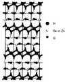
CAAC에 포함되는 결정 구조의 일례에 대해서 도 15a 내지 15e, 도 16의 (a) 내지 (c), 및 도 17의 (a) 내지 (c)를 사용해서 상세하게 설명한다. 특히 다른 표시가 없는 한, 도 15a 내지 15e, 도 16의 (a) 내지 (c), 및 도 17의 (a) 내지 (c)는 상측 방향을 c축 방향으로 하고, c축 방향과 직교하는 면을 ab면으로 한다. 간단히 "상반부" 및 "하반부"라고 할 경우, ab면을 경계로 했을 경우의 상반부 및 하반부(ab면에 대해 상반부 및 하반부)를 말한다. 또한, 도 15a 내지 15e에 있어서, 원으로 둘러싸인 O는 4 배위의 O를 나타내고, 이중 원으로 둘러싸인 O는 3 배위의 O를 나타낸다.An example of the crystal structure included in the CAAC will be described in detail with reference to Figs. 15A to 15E, Figs. 16A to 16C, and Figs. 17A to 17C. 15A to 15E, Figs. 16A to 16C, and Figs. 17A to 17C, the upper side is referred to as a c-axis direction and the other side of the c- Let ab-face be the face. Quot; upper half "and" lower half "refer to the upper half and lower half (upper half and lower half with respect to the ab plane) when the ab plane is taken as a boundary. 15A to 15E, O enclosed in a circle represents O in four coordinates, and O enclosed in a double circle represents O in three coordinates.
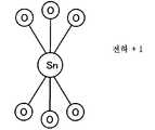
도 15a에, 1개의 6 배위의 In 원자와 In 원자에 근접한 6개의 4 배위의 산소 (이하 4 배위의 O) 원자를 포함하는 구조를 나타낸다. 여기에서는, 1개의 금속 원자와 이에 근접한 산소 원자를 포함하는 구조를 소그룹이라고 한다. 도 15a의 구조는 실제로 팔면체 구조를 취하지만, 간단화를 위하여 평면 구조로 나타내고 있다. 도 15a의 상반부 및 하반부에는 각각 3개씩 4 배위의 O 원자가 있다는 점에 주목한다. 도 15a에 나타내는 소그룹에서, 전하는 0이다.Fig. 15A shows a structure containing one six-coordinate of In atoms and six four-coordinate oxygens close to the In atoms (hereinafter referred to as four-coordinate O atoms). Herein, a structure including one metal atom and an oxygen atom adjacent thereto is referred to as a small group. The structure of Fig. 15A actually takes an octahedral structure, but is shown as a planar structure for simplification. Note that there are three O atoms in four coordinates in the upper half and the lower half of Fig. 15A, respectively. In the small group shown in Fig. 15A, the charge is zero.
도 15b에, 1개의 5 배위의 Ga 원자와, Ga 원자에 근접한 3개의 3 배위의 산소(이하 3 배위의 O) 원자와, Ga 원자에 근접한 2개의 4 배위의 O 원자를 포함하는 구조를 나타낸다. 3 배위의 O 원자는 모두 ab면에 존재한다. 도 15b의 상반부 및 하반부에는 각각 1개씩 4 배위의 O 원자가 있다. In 원자는 5 배위를 취할 수 있기 때문에 In 원자는 또한 도 15b에 나타내는 구조를 취할 수 있다. 도 15b에 나타내는 소그룹에서, 전하는 0이다.15B shows a structure including one five-coordinate Ga atom, three three-coordinate oxygen atoms adjacent to the Ga atom (hereinafter referred to as O atom) and two four-coordinate O atoms close to the Ga atom . The O atoms in the triplet are all present on the ab plane. In the upper half and lower half of Fig. 15B, there are O atoms of four coordinates each. Since the In atom can take five coordinates, the In atom can also take the structure shown in Fig. 15B. In the small group shown in Fig. 15B, the charge is zero.
도 15c에, 1개의 4 배위의 Zn 원자와 Zn 원자에 근접한 4개의 4 배위의 O 원자를 포함하는 구조를 나타낸다. 도 15c에서, 상반부에는 1개의 4 배위의 O 원자가 있고, 하반부에는 3개의 4 배위의 O 원자가 있다. 또는, 도 15c에서, 상반부에 3개의 4 배위의 O 원자가 있고, 하반부에 1개의 4 배위의 O 원자가 있어도 된다. 도 15c에 나타내는 소그룹에서, 전하는 0이다.Fig. 15 (c) shows a structure containing one Zn atom in four coordinates and four O atoms in four coordinates close to the Zn atom. In Fig. 15C, there are one four-coordinate O atom in the upper half, and three four-coordinate coordinates in the lower half. Alternatively, in Fig. 15C, there may be three O atoms of four coordinates in the upper half and one O atom of four coordinates in the lower half. In the small group shown in Fig. 15C, the charge is zero.
도 15d에, 1개의 6 배위의 Sn 원자와 Sn 원자에 근접한 6개의 4 배위의 O 원자를 포함하는 구조를 나타낸다. 도 15d에서, 상반부 및 하반부 각각에는 3개의 4 배위의 O 원자가 있다. 도 15d에 나타내는 소그룹에서, 전하는 +1이다.Fig. 15D shows a structure containing one Sn atom in six coordinates and six four-coordinate O atoms close to Sn atom. In Fig. 15D, there are three 4-coordinate O atoms in each of the upper half and the lower half. In the small group shown in Fig. 15D, the charge is +1.
도 15e에, 2개의 Zn 원자를 포함하는 소그룹을 나타낸다. 도 15e에서, 상반부 및 하반부 각각에는 1개의 4 배위의 O 원자가 있다. 도 15e에 나타내는 소그룹에서, 전하는 -1이다.Fig. 15E shows a small group containing two Zn atoms. In Fig. 15E, there are one four-coordinate O atom in each of the upper half and the lower half. In the small group shown in FIG. 15E, the charge is -1.
여기에서는, 복수의 소그룹은 중간 그룹을 형성하고, 복수의 중간 그룹은 대그룹(유닛 셀이라고도 한다)을 형성한다.Here, a plurality of small groups form an intermediate group, and a plurality of intermediate groups form a large group (also referred to as a unit cell).
이제, 이들의 소그룹끼리가 결합하는 규칙에 대해서 설명한다. 도 15a의 6 배위의 In 원자의 상반부의 3개의 O 원자는 하측 방향에 각각 3개의 근접 In 원자를 갖고, 하반부의 3개의 O 원자는 상측 방향에 각각 3개의 근접 In 원자를 갖는다. 5 배위의 Ga 원자의 상반부의 1개의 O 원자는 하측 방향에 1개의 근접 Ga 원자를 갖고, 하반부의 1개의 O 원자는 상측 방향에 1개의 근접 Ga 원자를 갖는다. 4 배위의 Zn 원자의 상반부의 1개의 O 원자는 하측 방향에 1개의 근접 Zn 원자를 갖고, 하반부의 3개의 O 원자는 상측 방향에 각각 3개의 근접 Zn 원자를 갖는다. 이와 같이, 금속 원자의 상측 방향의 4배위의 O 원자의 수는 4 배위의 O 원자 각각의 하측 방향에 있는 근접 금속 원자의 수와 동등하다. 마찬가지로, 금속 원자의 하측 방향의 4 배위의 O 원자의 수는 4 배위의 O 원자 각각의 상측 방향에 있는 근접 금속 원자의 수와 동등하다. O 원자의 배위는 4 배위이므로, O 원자의 하측 방향에 있는 근접 금속 원자의 수와 O 원자의 상측 방향에 있는 근접 금속 원자의 수의 합은 4가 된다. 따라서, 금속 원자의 상측 방향에 있는 4 배위의 O 원자의 수와 다른 금속 원자의 하측 방향에 있는 4 배위의 O 원자의 수의 합이 4일 때, 금속 원자를 포함하는 2종의 소그룹끼리는 결합할 수 있다. 예를 들어, 6 배위의 금속 (In 또는 Sn) 원자가 하반부의 3개의 4 배위의 O 원자를 개재해서 결합하는 경우에, 5 배위의 금속(Ga 또는 In) 원자 또는 4 배위의 금속(Zn) 원자와 결합하게 된다.Now, let's discuss the rules that these small groups join together. The three O atoms in the upper half of the In atom of the six coordination in Fig. 15A each have three nearby In atoms in the lower direction and the three O atoms in the lower half have three neighboring In atoms in the upper direction. One O atom in the upper half of the Ga atom in 5 coordination has one Ga atom in the lower direction and one O atom in the lower half has one Ga atom in the upper direction. One O atom in the upper half of the Zn atom in the 4-coordination has one proximal Zn atom in the lower direction and three O atoms in the lower half have three proximal Zn atoms in the upper direction. Thus, the number of O atoms in the 4-degree coordinate in the upward direction of the metal atom is equal to the number of the near-side metal atoms in the lower direction in each of the O atoms in the 4-coordinate degree. Likewise, the number of O atoms in the four coordinates in the lower direction of the metal atom is equivalent to the number of the nearby metal atoms in the upper direction of each of the O atoms in four coordinates. Since the coordination of the O atom is in four coordination, the sum of the number of the nearby metal atoms in the lower direction of the O atom and the number of the nearby metal atoms in the upper direction of the O atom is four. Therefore, when the sum of the number of O atoms in four coordinates in the upper direction of a metal atom and the number of O atoms in four coordinates in the lower direction of other metal atoms is 4, two small groups including a metal atom can do. For example, when a metal (In or Sn) atom of 6 coordination bonds through three 4-coordinate O atoms at the lower half, a metal (Ga or In) atom of 5 coordination or a metal (Zn) atom of 4 coordination Lt; / RTI >
상기 배위 수를 갖는 금속 원자는 c축 방향에 있어서 4 배위의 O 원자를 개재해서 다른 금속 원자와 결합한다. 상기 외에도, 층 구조의 합계의 전하가 0으로 되도록 복수의 소그룹을 결합해서 다른 방식으로 중간 그룹을 구성할 수 있다.The metal atom having the coordination number is bonded to another metal atom via the O atom in four coordinates in the c-axis direction. In addition to the above, a plurality of subgroups may be combined so that the total charge of the layer structure is zero to form an intermediate group in a different manner.
도 16의 (a)에, In-Sn-Zn-O계 재료의 층 구조에 포함되는 중간 그룹의 모델도를 나타낸다. 도 16의 (b)에, 3개의 중간 그룹을 포함하는 대그룹을 나타낸다. 도 16의 (c)는 도 16의 (b)의 층 구조를 c축 방향으로부터 관찰한 경우의 원자 배열을 나타낸다는 점에 주목한다.Fig. 16 (a) shows a model diagram of an intermediate group included in the layer structure of In-Sn-Zn-O-based material. FIG. 16 (b) shows a large group including three intermediate groups. 16 (c) shows that the layer structure of FIG. 16 (b) shows an atomic arrangement when observed from the c-axis direction.
도 16의 (a)에서, 간단화를 위하여 3 배위의 O 원자는 생략하고, 4 배위의 O 원자는 원으로 나타내고, 원 안의 수가 4 배위의 O 원자의 수를 나타낸다. 예를 들어, Sn 원자의 상반부 및 하반부에는 각각 3개씩 4 배위의 O 원자가 있는 것을 원으로 둘러싸인 3으로서 나타내고 있다. 마찬가지로, 도 16의 (a)에 있어서, In 원자의 상반부 및 하반부에는 각각 1개씩 4 배위의 O가 있는 것을 원으로 둘러싸인 1로서 나타내고 있다. 또한, 도 16의 (a)에서, 하반부에는 1개의 4 배위의 O 원자가 있고, 상반부에는 3개의 4 배위의 O 원자가 있는 Zn 원자와, 상반부에는 1개의 4 배위의 O 원자가 있고, 하반부에는 3개의 4 배위의 O 원자가 있는 Zn 원자를 나타내고 있다.In FIG. 16 (a), for simplification, the O atom at three coordinates is omitted, the O atom at four coordinates is represented by a circle, and the number of O atoms in the circle represents the number of O atoms at four coordinates. For example, in the upper half and lower half of the Sn atom, three O atoms each having four coordinates are shown as 3 surrounded by a circle. Similarly, in FIG. 16 (a), the upper half and the lower half of the In atoms each having O in four coordinates by one are shown as 1 surrounded by a circle. 16 (a), Zn atoms having one four-coordinated O atom in the lower half, three O atoms in three quadrants in the upper half, one O atom in four coordinates in the upper half, three Represents a Zn atom having an O atom in the 4-coordination.
도 16의 (a)에서의 In-Sn-Zn-O계 재료의 층 구조에 포함되는 중간 그룹에서, 위에서부터 순차적으로 4 배위의 O 원자가 3개씩 상반부 및 하반부에 있는 Sn 원자가, 4 배위의 O 원자가 1개씩 상반부 및 하반부에 있는 In 원자와 결합하고, In 원자가 상반부에 3개의 4 배위의 O 원자가 있는 Zn 원자와 결합하고, Zn 원자가 Zn 원자의 하반부의 1개의 4 배위의 O 원자를 개재해서 4 배위의 O 원자가 3개씩 상반부 및 하반부에 있는 In 원자와 결합하고, In 원자가 상반부에 1개의 4 배위의 O 원자가 있는 Zn 원자 2개를 포함하는 소그룹과 결합하고, 이 소그룹이 소그룹의 하반부의 1개의 4 배위의 O 원자를 개재해서 4 배위의 O 원자가 3개씩 상반부 및 하반부에 있는 Sn 원자와 결합한다. 이러한 복수의 중간 그룹이 결합해서, 대그룹을 구성한다.In the intermediate group included in the layer structure of the In-Sn-Zn-O-based material in FIG. 16 (a), Sn atoms in the upper and lower halves of three O atoms in four coordinates in order from the top sequentially, Atoms are bonded to the In atom at the upper half and the lower half of the atom by one atom, and the In atom binds to the Zn atom having three quadrature coordination O atoms at the upper half, and the Zn atom binds to 4 And the O atoms of the coordination are bonded to the In atoms at the upper and lower halves by three, and the In atoms are bonded to the small group containing two Zn atoms having one four-coordinate O atom in the upper half, and this small group is bonded to one Three O atoms of four coordination are bonded to the Sn atom in the upper half and the lower half through the O atom of the four coordination. These plural intermediate groups combine to form a large group.
여기서, 3 배위의 O 원자 및 4 배위의 O 원자의 경우, 결합 1개 당의 전하는 각각 -0.667 및 -0.5로 생각할 수 있다. 예를 들어, In 원자(6 배위 또는 5 배위), Zn 원자(4 배위), 및 Sn 원자(5 배위 또는 6 배위)의 전하는 각각 +3, +2, 및 +4이다. 따라서, Sn 원자를 포함하는 소그룹은 전하가 +1이 된다. 그로 인해, Sn 원자를 포함하는 층 구조를 형성하기 위해서는, 전하 +1을 상쇄하는 전하 -1이 필요해진다. 전하 -1을 취하는 구조로서, 도 15e에 도시한 바와 같이, 2개의 Zn 원자를 포함하는 소그룹을 들 수 있다. 예를 들어, Sn 원자를 포함하는 소그룹 1개에 대하여, 2개의 Zn 원자를 포함하는 소그룹이 1개 있으면, 전하가 상쇄되기 때문에, 층 구조의 합계의 전하를 0으로 할 수 있다.Here, in the case of O atoms of three coordinates and O atoms of four coordinates, the charge per one bond can be considered to be -0.667 and -0.5, respectively. For example, the electric charges of In atom (6 coordination or 5 coordination), Zn atom (4 coordination), and Sn atom (5 coordination or 6 coordination) are +3, +2, and +4, respectively. Thus, a small group containing Sn atoms has a charge of +1. Therefore, in order to form a layer structure including a Sn atom, a charge-1 canceling a charge + 1 is required. As a structure taking charge-1, there is a small group containing two Zn atoms, as shown in Fig. 15E. For example, if there is one small group containing two Zn atoms in one small group containing Sn atoms, since the charge is canceled, the total charge of the layer structure can be made zero.
도 16의 (b)에 나타낸 대그룹이 반복될 때, In-Sn-Zn-O계의 결정(In2SnZn3O8)을 얻을 수 있다. 얻어지는 In-Sn-Zn-O계의 결정의 층 구조는 In2SnZn2O7(ZnO)m (m은 0 또는 자연수)로 하는 조성식으로 표현할 수 있다는 점에 주목한다.When the large group shown in FIG. 16 (b) is repeated, a crystal of In-Sn-Zn-O system (In2 SnZn3 O8 ) can be obtained. Note that the layer structure of the resulting In-Sn-Zn-O system crystal can be expressed by a composition formula of In2 SnZn2 O7 (ZnO)m (m is 0 or a natural number).
상술한 규칙은, 4원계 금속의 산화물인 In-Sn-Ga-Zn계 산화물; 3원계 금속의 산화물인 In-Ga-Zn계 산화물(IGZO라고도 표기한다), In-Al-Zn계 산화물, Sn-Ga-Zn계 산화물, Al-Ga-Zn계 산화물, Sn-Al-Zn계 산화물, In-Hf-Zn계 산화물, In-La-Zn계 산화물, In-Ce-Zn계 산화물, In-Pr-Zn계 산화물, In-Nd-Zn계 산화물, In-Sm-Zn계 산화물, In-Eu-Zn계 산화물, In-Gd-Zn계 산화물, In-Tb-Zn계 산화물, In-Dy-Zn계 산화물, In-Ho-Zn계 산화물, In-Er-Zn계 산화물, In-Tm-Zn계 산화물, In-Yb-Zn계 산화물, 또는 In-Lu-Zn계 산화물; 2원계 금속의 산화물인 In-Zn계 산화물, Sn-Zn계 산화물, Al-Zn계 산화물, Zn-Mg계 산화물, Sn-Mg계 산화물, In-Mg계 산화물 또는, In-Ga계 산화물 등을 사용했을 경우도 마찬가지이다.The above-mentioned rule is that an In-Sn-Ga-Zn-based oxide which is an oxide of a quaternary metal; An In-Ga-Zn-based oxide (also referred to as IGZO), an In-Al-Zn-based oxide, a Sn-Ga-Zn-based oxide, an Al- Zn-based oxide, In-Sm-Zn-based oxide, In-Hf-Zn-based oxide, In-La-Zn-based oxide, In- Zn-based oxide, In-Zn-based oxide, In-Gd-Zn-based oxide, In-Tb-Zn-based oxide, In- Tm-Zn-based oxide, In-Yb-Zn-based oxide, or In-Lu-Zn-based oxide; An In-Zn-based oxide, an Al-Zn-based oxide, a Zn-Mg-based oxide, a Sn-Mg-based oxide, an In-Mg-based oxide, or an In- The same is true when used.
예를 들어, 도 17의 (a)에, In-Ga-Zn-O계 재료의 층 구조에 포함되는 중간 그룹의 모델도를 나타낸다.For example, Fig. 17 (a) shows a model diagram of an intermediate group included in the layer structure of the In-Ga-Zn-O-based material.
도 17의 (a)에서의 In-Ga-Zn-O계 재료의 층 구조에 포함되는 중간 그룹에서, 위에서부터 순차적으로 4 배위의 O 원자가 3개씩 상반부 및 하반부에 있는 In 원자가 4 배위의 O 원자가 1개 상반부에 있는 Zn 원자와 결합하고, Zn 원자는 Zn 원자의 하반부의 3개의 4 배위의 O 원자를 개재하여 4 배위의 O 원자가 1개씩 상반부 및 하반부에 있는 Ga 원자와 결합하고, Ga 원자는 Ga 원자의 하반부의 1개의 4 배위의 O 원자를 개재하여 4 배위의 O 원자가 3개씩 상반부 및 하반부에 있는 In 원자와 결합한다. 이러한 복수의 중간 그룹이 결합해서, 대그룹을 구성한다.In the middle group included in the layer structure of the In-Ga-Zn-O-based material in FIG. 17A, three O atoms of four coordinates in the order from the top are sequentially arranged in the upper half and the lower half, And the Zn atom is bonded to the Ga atoms in the upper half and the lower half through the O atoms of four coordinates in the lower half of the Zn atom by three O atoms in four coordinates, Through the O atom of one of the four coordinates in the lower half of the Ga atom, the O atom at four coordinates is bonded to the In atom at the upper half and the lower half by three O atoms. These plural intermediate groups combine to form a large group.
도 17의 (b)에 3개의 중간 그룹을 포함하는 대그룹을 나타낸다. 도 17의 (c)는 도 17의 (b)의 층 구조를 c축 방향으로부터 관찰한 경우의 원자 배열을 나타내고 있다는 점에 주목한다.FIG. 17 (b) shows a large group including three intermediate groups. 17 (c) shows the atomic arrangement when the layer structure of FIG. 17 (b) is observed from the c-axis direction.
여기서, In 원자(6 배위 또는 5 배위), Zn 원자(4 배위), 및 Ga 원자(5 배위)의 전하는, 각각 +3, +2, 및 +3이기 때문에, In, Zn 및 Ga 중 어느 하나를 포함하는 소그룹의 전하가 0이 된다. 그로 인해, 이러한 소그룹의 조합을 포함하는 중간 그룹의 합계의 전하는 항상 0이 된다.Since the electric charges of the In atom (6 coordination or 5 coordination), Zn atom (4 coordination) and Ga atom (5 coordination) are +3, +2 and +3, The charge of the small group including the group becomes zero. As a result, the charge of the sum of the intermediate groups including the combination of these small groups is always zero.
In-Ga-Zn-O계 재료의 층 구조를 구성하기 위해서, 대그룹은 도 17의 (a)에 나타낸 중간 그룹뿐만 아니라, In 원자, Ga 원자, 및 Zn 원자의 배열이 도 17의 (a)의 것과 다른 중간 그룹을 사용하여 구성할 수 있다.In order to form the layer structure of the In-Ga-Zn-O-based material, in the large group, not only the intermediate group shown in FIG. 17A, but also the arrangement of the In, Ga, Lt; RTI ID = 0.0 > and / or < / RTI >
도 17의 (b)에 나타낸 대그룹이 반복될 때, In-Ga-Zn-O계의 결정을 얻을 수 있다. 얻어지는 In-Ga-Zn-O계 결정의 층 구조는 InGaO3(ZnO)n (n은 자연수)로 하는 조성식으로 표현할 수 있다는 점에 주목한다.When the large group shown in Fig. 17 (b) is repeated, crystals of In-Ga-Zn-O system can be obtained. Note that the layer structure of the obtained In-Ga-Zn-O-based crystal can be expressed by a composition formula of InGaO3 (ZnO)n (n is a natural number).
n=1(InGaZnO4)의 경우에는, 예를 들어, 도 32a에 나타내는 결정 구조를 취할 수 있다. 도 32a에 나타내는 결정 구조에 있어서, 도 15b에서 설명한 바와 같이 Ga 원자 및 In 원자는 5 배위를 취하기 때문에, Ga가 In으로 치환된 구조도 취할 수 있다는 점에 주목한다.In the case of n = 1 (InGaZnO4 ), for example, the crystal structure shown in Fig. 32A can be obtained. Note that in the crystal structure shown in Fig. 32A, since Ga atoms and In atoms take five coordinates as described in Fig. 15B, it is also possible to adopt a structure in which Ga is substituted with In.
n=2(InGaZn2O5)의 경우에는, 예를 들어 도 32b에 나타내는 결정 구조를 취할 수 있다. 도 14b에 나타내는 결정 구조에 있어서, 도 32b에서 설명한 바와 같이, Ga 원자 및 In 원자는 5 배위를 취하기 때문에, Ga가 In으로 치환된 구조도 취할 수 있다는 점에 주목한다.In the case of n = 2 (InGaZn2 O5 ), for example, the crystal structure shown in FIG. 32B can be obtained. Note that in the crystal structure shown in Fig. 14B, since Ga atoms and In atoms take five coordinates as described in Fig. 32B, it is also possible to adopt a structure in which Ga is substituted with In.
트랜지스터(160) 및 트랜지스터(162)는 n 채널형 트랜지스터 또는 p 채널형 트랜지스터를 사용할 수 있다. 여기에서는, 트랜지스터(160 및 162)는 n채널형 트랜지스터로 하는 경우에 대해 설명한다. 여기에 개시하는 본 발명의 기술적인 특징은 데이터를 유지하기 위해서 산화물 반도체 등의, 오프 전류를 충분히 저감하는 것이 가능한 반도체 재료를 트랜지스터(162)에 사용한다는 점에 있다. 그러므로, 반도체 장치의 재료나 구조 등의 구체적인 조건을 여기에 주어진 것에 한정할 필요는 없다.The
트랜지스터(160)는 반도체 기판(500) 위의 반도체층에 설치된 채널 형성 영역(134)과, 채널 형성 영역(134)을 사이에 두고 설치된 불순물 영역(132)(소스 영역 또는 드레인 영역이라고도 한다)과, 채널 형성 영역(134) 위에 설치된 게이트 절연층(122a)과, 채널 형성 영역(134)과 중첩하도록 게이트 절연층(122a) 위에 설치된 게이트 전극(128a)을 포함한다. 도면에 있어서, 명시적으로는 소스 전극이나 드레인 전극을 도시하지 않는 트랜지스터를, 편의상, 트랜지스터라고 한다는 점에 주목한다. 또한, 이러한 경우, 트랜지스터의 접속 관계를 설명하기 위해서, 소스 영역이나 드레인 영역을 포함해서 "소스 전극"이나 "드레인 전극"이라고 표현하는 경우가 있다. 즉, 본 명세서에 있어서, "소스 전극"이라는 기재에는 소스 영역이 포함될 수 있다.The
또한, 반도체 기판(500) 위의 반도체층에 설치된 불순물 영역(126)에는 도전층(128b)이 접속되어 있다. 여기서, 도전층(128b)은 트랜지스터(160)의 소스 전극 또는 드레인 전극으로서 기능한다. 또한, 불순물 영역(132)과 불순물 영역 (126) 사이에는 불순물 영역(130)이 설치되어 있다. 여기서, 불순물 영역(126) 및 불순물 영역(130)도 트랜지스터(160)의 소스 영역 또는 드레인 영역으로서 기능할 수 있다. 도전층(128b)을 반드시 설치할 필요는 없다는 점에 주목한다. 그 경우, 불순물 영역(126), 불순물 영역(130), 및 불순물 영역(132)은 트랜지스터(160)의 소스 영역 또는 드레인 영역으로서 기능하는 불순물 영역으로서 하나에 통합해도 된다.A
트랜지스터(160)를 덮도록 절연층(136), 절연층(138), 및 절연층(140)이 적층되어 있다. 트랜지스터(160)를 덮는 절연층의 구조는 반드시 적층 구조일 필요는 없고, 단층 구조로 해도 된다는 점에 주목한다. 또한, 2층 이상의 적층 구조가 채용될 수 있다.An insulating
고집적화를 실현하기 위해서는, 도 1a 및 1b에 도시한 바와 같이 트랜지스터(160)가 측벽 절연층을 포함하지 않는 구성으로 하는 것이 바람직하다는 점에 주목한다. 한편, 트랜지스터(160)의 특성을 중시하는 경우에는, 게이트 전극(128a)의 측면에 측벽 절연층을 설치할 수 있고, 불순물 영역(132)은 그 측벽 절연층과 중첩하는 영역에 형성된 불순물 농도가 상이한 불순물 영역을 포함할 수 있다.Note that in order to achieve high integration, it is preferable that the
도 1a 및 1b에 도시하는 반도체 장치에 있어서는, 반도체 기판(500) 위로 산화막(512)을 개재해서 설치된 반도체층을 사용해서 트랜지스터(160)의 채널 형성 영역(134) 및 불순물 영역(126)을 형성하고 있지만, 본 발명의 한 실시 형태는 이것에 한정되지 않는다는 점에 주목한다. 예를 들어, 반도체 기판(500) 대신에, 알루미노실리케이트 유리 기판, 알루미노보로실리케이트 유리 기판, 또는 바륨 보로실리케이트 유리 기판 등의, 전자 공업용으로 사용되는 각종 유리 기판; 석영 기판; 세라믹 기판 또는 사파이어 기판을 사용할 수 있다. 또한, 질화 실리콘과 산화 알루미늄을 주성분으로 포함하고 열팽창 계수가 실리콘의 것과 가까운 세라믹 기판을 사용할 수 있다. 또한, 산화막(512) 위에 반도체층을 형성하지 않고 반도체 기판(500) 위에 채널 형성 영역이나 불순물 영역을 직접 설치할 수 있다. 그 경우, 트랜지스터(160)가 전기적으로 분리되도록, 트랜지스터(160)를 덮도록 소자 분리 절연층을 설치한다.1A and 1B, a
트랜지스터(162)는 절연층(140) 등 위에 설치된 산화물 반도체층(144)과, 산화물 반도체층(144)과 전기적으로 접속되어 있는 소스 전극(또는 드레인 전극) (142a) 및 드레인 전극(또는 소스 전극)(142b)과, 산화물 반도체층(144), 소스 전극(142a) 및 드레인 전극(142b)을 덮는 게이트 절연층(146)과, 게이트 절연층(146) 위에 산화물 반도체층(144)과 중첩하도록 설치된 게이트 전극(148a)을 포함한다. 여기서, 트랜지스터(162)의 드레인 전극(142b)은 트랜지스터(160)의 게이트 전극(128a)과 접속된다. 따라서, 트랜지스터(162)의 전하 리텐션 특성을 살리기 위해 트랜지스터(160)의 게이트 전극(128a)의 전위를 극히 장기간에 걸쳐서 유지할 수 있다. 또한, 산화물 반도체층(144)은 트랜지스터(162)의 채널 형성 영역으로서 기능하고, 적어도 트랜지스터(160)의 소스 영역 또는 드레인 영역의 일부와 중첩하도록 설치된다.The
여기서, 트랜지스터(162)에 사용되는 산화물 반도체층(144)은 수소 등의 불순물이 충분히 제거됨으로써 또는 충분한 산소가 공급됨으로써 고순도화되는 것이 바람직하다. 구체적으로는, 산화물 반도체층(144)의 수소 농도는 5×10¹⁹원자/cm3 이하, 바람직하게는 5×10¹⁸원자/cm3 이하, 보다 바람직하게는 5×10¹⁷원자/cm3 이하로 한다. 상술한 산화물 반도체층(144)의 수소 농도는 2차 이온 질량 분석법(SIMS)으로 측정된다는 점에 주목한다. 수소 농도가 충분히 저감되어서 고순도화되어, 충분한 산소의 공급에 의해 산소 결핍에 기인하는 에너지 갭 중의 결함 준위가 저감된 산화물 반도체층(144)에서는, 캐리어 농도가 1×10¹²/cm3 미만, 바람직하게는, 1×10¹¹/cm3 미만, 보다 바람직하게는 1.45×10¹⁰/cm3 미만이 된다. 예를 들어, 실온(25℃)에서의 오프 전류(여기서는, 단위 채널 폭의 마이크로미터(μm) 당의 전류)는 100zA(1zA(젭토 암페어)은 1×10-21A) 이하, 바람직하게는 10zA 이하가 된다. 이와 같이, i형화 (진성화) 산화물 반도체 또는 실질적으로 i형화된 산화물 반도체층(144)을 사용함으로써 극히 우수한 오프 전류 특성의 트랜지스터(162)를 얻을 수 있다.Here, it is preferable that the
산화물 반도체층(144)의 나트륨 농도는 5×10¹⁶원자/cm3 이하, 바람직하게는 1×10¹⁶원자/cm3 이하, 더욱 바람직하게는 1×10¹⁵원자/cm3 이하로 한다. 또한, 산화물 반도체층(144)의 리튬 농도는 5×10¹⁵원자/cm3 이하, 바람직하게는 1×10¹⁵원자/cm3 이하로 한다. 산화물 반도체층(144)의 칼륨 농도는 5×10¹⁵원자/cm3 이하, 바람직하게는 1×10¹⁵원자/cm3 이하로 한다. 상술한 산화물 반도체층(144) 중의 나트륨 농도, 리튬 농도 및 칼륨 농도는 2차 이온 질량 분석법으로 측정되는 것이다. 알칼리 금속 및 알칼리 토금속은 산화물 반도체에 있어서는 악성인 불순물이며, 가능한 한 적게 포함되는 것이 좋다. 특히, 알칼리 금속 중, 나트륨은 산화물 반도체에 접하는 절연막이 산화물인 경우, 산화물 안에 확산하고, Na+이 된다. 또한, 나트륨은 산화물 반도체 내에서 금속과 산소의 결합을 분단하고, 또는 결합에 들어간다. 그 결과, 트랜지스터 특성의 열화(예를 들어, 트랜지스터의 노멀리 온화(임계값의 부측으로의 시프트) 또는 이동도의 저하)를 초래한다. 더구나, 이것은 특성의 변동의 원인이 된다. 이러한 문제는 특히 산화물 반도체 중의 수소의 농도가 충분히 낮은 경우에 있어서 현저해진다. 따라서, 산화물 반도체 중의 수소의 농도가 5×1019cm-3 이하, 특히 5×1018cm-3 이하인 경우에는, 알칼리 금속의 농도를 상기의 값으로 하는 것이 강하게 요구된다.The concentration of sodium in the
트랜지스터(162)에는 미세화에 기인해서 소자 간에 발생하는 누설 전류를 억제하기 위해서 섬 형상으로 가공된 산화물 반도체층(144)이 포함되어 있지만, 산화물 반도체층이 섬 형상으로 가공되어 있지 않은 구성을 채용해도 된다는 점에 주목한다. 산화물 반도체층을 섬 형상으로 가공하지 않을 경우에는, 가공 시의 에칭에 의한 산화물 반도체층의 오염을 방지할 수 있다.Although the
용량 소자(164)는 드레인 전극(142b), 게이트 절연층(146), 및 도전층(148b) 을 포함한다. 즉, 드레인 전극(142b)은 용량 소자(164)의 한쪽의 전극으로서 기능하고, 도전층(148b)은 용량 소자(164)의 다른 쪽의 전극으로서 기능하게 된다. 이러한 구성으로 함으로써, 충분한 용량을 확보할 수 있다. 또한, 용량 소자(164)에서, 산화물 반도체층(144)과 게이트 절연층(146)을 적층시킴으로써, 드레인 전극(142b)과 도전층(148b) 간의 절연성을 적당히 확보할 수 있다. 또한, 용량이 불필요한 경우에는 용량 소자(164)를 생략할 수 있다.The
트랜지스터(162) 및 용량 소자(164)에 있어서, 소스 전극(142a) 및 드레인 전극(142b)의 단부는 테이퍼 형상인 것이 바람직하다는 점에 주목한다. 소스 전극(142a) 및 드레인 전극(142b)의 단부를 테이퍼 형상으로 함으로써, 게이트 절연층(146)의 피복성을 향상시켜서, 그 절단을 방지할 수 있다. 여기서, 테이퍼 각은, 예를 들어 30°이상 60°이하로 한다. 테이퍼 각은 테이퍼 형상을 갖는 층 (예를 들어, 소스 전극(142a))을 층의 단면(기판의 표면과 직교하는 면)에 수직인 방향으로부터 관찰했을 때에, 이 층의 측면과 저면이 이루는 경사각을 나타낸다는 점에 주목한다.Note that the ends of the
트랜지스터(162) 및 용량 소자(164) 위에는 절연층(150)이 설치되어 있다. 배선(154)은 절연층(150) 위에 설치되고, 게이트 절연층(146), 절연층(150) 등에 형성된 개구를 개재해서 소스 전극(142a)과 접속되어 있다. 여기서, 배선(154)은 적어도 트랜지스터(162)의 산화물 반도체층(144)의 일부와 중첩하도록 설치되는 것이 바람직하다. 또한, 배선(154) 위로 절연층(156)을 설치해도 된다. 도 1a 및 1b에서는 도전층(128b)을 통해 배선(154), 소스 전극(142a), 및 불순물 영역(126)을 서로 접속하고 있지만, 본 발명의 한 실시 형태는 이것에 한정되지 않는다는 점에 주목한다. 예를 들어, 소스 전극(142a)을 직접 불순물 영역(126)에 접촉시킬 수 있다. 또는, 배선(154)을 다른 도전층을 개재하여 소스 전극(142a)에 접촉시킬 수 있다.An insulating
도 1a 및 1b에 도시된 반도체 장치에서, 트랜지스터(160)와 트랜지스터(162)는 적어도 일부가 서로 중첩하도록 설치되어 있다. 특히, 트랜지스터(160)의 소스 영역 또는 드레인 영역과 산화물 반도체층(144)의 적어도 일부가 서로 중첩하도록 설치되어 있다. 배선(154)은 적어도 산화물 반도체층(144)의 일부와 중첩하도록 설치되어 있다. 또한, 트랜지스터(162), 용량 소자(164) 등은 트랜지스터(160)와 중첩하도록 설치되어 있다. 예를 들어, 용량 소자(164)의 도전층(148b)은 트랜지스터(160)의 게이트 전극(128a)과 적어도 일부가 중첩하도록 설치되어 있다. 이러한 평면 레이아웃을 채용함으로써, 반도체 장치의 고집적화를 도모할 수 있다. 예를 들어, 이 반도체 장치를 사용해서 메모리 셀을 구성하는 경우에, 최소 가공 치수를 F라고 하면, 메모리 셀이 차지하는 면적을 대략 15 F2 내지 25 F2로 하는 것이 가능하다.In the semiconductor device shown in Figs. 1A and 1B, the
그러나, 트랜지스터(160)와 트랜지스터(162)가 적어도 일부가 서로 중첩하도록 설치되는 경우에, 트랜지스터(160)의 소스 영역 또는 드레인 영역이 트랜지스터(162)의 백 게이트 전극으로서 기능할 수 있다. 특히, 도 1b에 도시한 바와 같이, 산화물 반도체층(144)이 트랜지스터(160)의 소스 영역 또는 드레인 영역 위에 가로질러 형성되는 경우에, 트랜지스터(160)의 소스 영역 또는 드레인 영역이 백 게이트 전극으로서 기능할 수 있다. 여기에서 백 게이트 전극이란 산화물 반도체층(144)의 채널 형성 영역을 사이에 두고 게이트 전극(148a)과는 반대측에 설치된 의사(pseudo) 게이트 전극을 말한다는 점에 주목한다. 즉, 트랜지스터(160)의 소스 영역 또는 드레인 영역에 정(positive)의 전위가 부여되고, 그 정의 전위가 백 게이트 전극에 의해 설정된 임계값 전압 Vth(back)을 초과하면, 트랜지스터(162)는 온 상태가 된다. 트랜지스터(160)의 소스 영역 또는 드레인 영역에 부여된 정의 전위가 트랜지스터(162)를 온 상태로 하지 않는 정도의 크기이어도, 트랜지스터(162)의 게이트 전극(148a)에 의해 설정된 임계값 전압 Vth은 부(트랜지스터(162)가 노멀리 온화)로 시프트된다. 예를 들어, 반도체 장치의 판독 동작 또는 기입 동작에 있어서 트랜지스터(160)의 소스 영역 또는 드레인 영역에 정의 전위가 부여될 경우, 트랜지스터(162)의 임계값 전압 Vth는 부(트랜지스터(162)가 노멀리 온화)로 시프트되고, 트랜지스터(162)의 누설 전류가 증가하여, 전하의 리텐션 특성이 저하하게 된다. 특히, 본 실시 형태에 따른 반도체 장치를 사용해서 메모리 셀 어레이 등을 구성하는 경우에, 트랜지스터(160)의 게이트 전극(128a)에 유지되어 있는 전하가 상실되는 것에 의해, 이 메모리 셀의 데이터가 변동할 수 있다. 즉, 반도체 장치의 메모리 리텐션 특성이 저하할 수 있다. 메모리 리텐션 특성이란 메모리의 데이터 유지 특성을 말한다는 점에 주목한다.However, the source region or the drain region of the
상기를 감안하여, 개시하는 발명의 한 실시 형태의 반도체 장치에 있어서는, 트랜지스터(160)의 게이트 전극(128a)에 전하를 유지해야 할 기간, 즉 트랜지스터(162)를 오프 상태로 해야 할 기간에 있어서, 적어도 트랜지스터(160)의 소스 영역 또는 드레인 영역에 정의 전위가 부여될 때에는, 게이트 전극(148a)에 부의 전위가 부여되도록 한다. 여기서, 게이트 전극(148a)에 부여되는 부의 전위의 크기는, 트랜지스터(160)의 소스 영역 또는 드레인 영역에 부여된 정의 전위가 미치는 트랜지스터(162)에의 영향을 억제할 수 있도록, 적절히 설정할 수 있다.In view of the above, in the semiconductor device according to the embodiment of the disclosed invention, in a period during which charge is to be held in the
구체적으로, 게이트 전극(148a)에 부여되는 부의 전위 Va는 트랜지스터(160)의 소스 영역 또는 드레인 영역에 부여되는 정의 전위 Vb, 트랜지스터(160)의 소스 영역 또는 드레인 영역과 산화물 반도체층(144) 사이에 설치된 절연층(도 1a 및 1b에 도시하는 반도체 장치에 있어서는, 게이트 절연층(122a), 절연층(136), 절연층(138) 및 절연층(140))의 두께 tb 및 합성 비유전율 εrb, 게이트 절연층 (146)의 두께 ta 및 비유전율 εra를 사용해서 표현한 하기의 수학식 1을 만족하는 것이 바람직하다.Specifically, the negative potential Va applied to the

즉, 부의 전위 Va는 정의 전위 Vb, 두께 tb, 합성 비유전율 εrb, 두께 ta 및 비유전율 εra에 따라 적절히 설정할 수 있다.That is, the negative potential Va can be appropriately set in accordance with the positive potential Vb , the thickness tb , the synthetic relative dielectric constant ∈rb , the thickness ta, and the relative dielectric constant ∈ra .
또한, 트랜지스터(162)를 오프 상태로 해야 할 기간에 있어서, 적어도 트랜지스터(160)의 소스 영역 또는 드레인 영역에 정의 전위가 부여될 때에는, 게이트 전극(148a)에 부의 전위가 부여된다. 예를 들어, 트랜지스터(162)가 오프 상태일 때는 항상 게이트 전극(148a)에 이 부의 전위가 부여되는 것으로 유지된다.When the positive potential is applied to at least the source region or the drain region of the
이러한 방식으로, 게이트 전극(148a)에 부의 전위가 부여되기 때문에, 트랜지스터(160)의 소스 영역 및 드레인 영역이 트랜지스터(162)의 백 게이트 전극으로서 기능하여도, 게이트 전극(148a)의 전위가 트랜지스터(162)의 임계값 전압보다 작아진다. 이에 의해, 트랜지스터(162)의 소스 전극과 드레인 전극 간에 발생한 누설 전류에 의해 메모리 셀의 데이터가 변동하는 것을 방지할 수 있다. 따라서, 본 실시 형태에 따른 반도체 장치의 메모리 리텐션 특성을 향상시킬 수 있다.In this way, even if the source region and the drain region of the
도 1a 및 1b에 도시하는 반도체 장치에 있어서는, 트랜지스터(162)로서 톱 게이트 구조의 트랜지스터를 사용했지만, 본 실시 형태에 따른 반도체 장치는 이것에 한정되는 것이 아니다. 예를 들어, 도 2a 및 2b에 도시하는 반도체 장치와 같이, 트랜지스터(162)로서 보텀 게이트 구조의 트랜지스터를 사용할 수 있다.In the semiconductor device shown in Figs. 1A and 1B, a transistor having a top gate structure is used as the
도 2a 및 2b에 도시하는 반도체 장치의 트랜지스터(162)는 게이트 전극(148a)과, 게이트 전극(148a)을 덮는 게이트 절연층(146)과, 게이트 절연층(146) 위로 게이트 전극(148a)과 중첩하도록 설치된 산화물 반도체층(144)과, 절연층(140) 등 위에 형성된, 산화물 반도체층(144)과 전기적으로 접속되어 있는 소스 전극(142a) 및 드레인 전극(142b)을 포함한다. 상세에 대해서는, 도 1a 및 1b에 도시하는 반도체 장치의 기재를 참조할 수 있다.The
또한, 도 2a 및 2b에 도시하는 반도체 장치에 있어서는, 트랜지스터(162) 위로 절연층(157)이 설치되고, 절연층(157) 위로 드레인 전극(142b)과 적어도 일부가 중첩하도록 도전층(158)이 설치된다. 즉, 도전층(158)은 용량 소자(164)의 한쪽의 전극으로서 기능한다. 여기서, 절연층(157)은 게이트 절연층(146)과 마찬가지인 재료로 형성할 수 있고, 도전층(158)은 도 1a 및 1b에 도시하는 도전층(148b)과 마찬가지인 재료로 형성할 수 있다. 상세에 대해서는, 도 1a 및 1b에 도시하는 반도체 장치의 기재를 참조할 수 있다.2A and 2B, an insulating
절연층(157) 및 도전층(158) 위에는 절연층(150)이 설치되어 있다. 배선(154)은 절연층(150) 위에 설치되고, 게이트 절연층(146), 절연층(150) 등에 형성된 개구를 개재해서 소스 전극(142a)과 접속되어 있다. 여기서, 배선(154)은 적어도 트랜지스터(162)의 산화물 반도체층(144)의 일부와 중첩하도록 설치된다. 상세에 대해서는, 도 1a 및 1b에 도시하는 반도체 장치의 기재를 참조할 수 있다.An insulating
다른 부분의 구조에 대해서는, 도 1a 및 1b에 도시하는 반도체 장치와 마찬가지이므로, 상세에 대해서는 이 반도체 장치의 기재를 참조할 수 있다는 점에 주목한다.Note that the structure of the other portions is the same as that of the semiconductor device shown in Figs. 1A and 1B, and therefore, the details of this semiconductor device can be referred to.
도 2a 및 2b에 도시하는 반도체 장치에 있어서, 트랜지스터(160)와 트랜지스터(162)는 적어도 일부가 서로 중첩하도록 설치되어 있다. 특히, 트랜지스터(160)의 소스 영역 또는 드레인 영역과 산화물 반도체층(144)의 일부가 서로 중첩하도록 설치되어 있다. 배선(154)은 적어도 산화물 반도체층(144)의 일부와 중첩하도록 설치되어 있다. 또한, 트랜지스터(162), 용량 소자(164) 등은 트랜지스터(160)와 중첩하도록 설치되어 있다. 예를 들어, 용량 소자(164)의 도전층(148b)은 트랜지스터(160)의 게이트 전극(128a)과 적어도 일부가 중첩하도록 설치되어 있다. 이러한 평면 레이아웃을 채용함으로써, 반도체 장치의 고집적화를 도모할 수 있다. 예를 들어, 이 반도체 장치를 사용해서 메모리 셀을 구성하는 경우, 최소 가공 치수를 F라고 하면, 메모리 셀이 차지하는 면적을 대략 15 F2 내지 25 F2로 하는 것이 가능하다.In the semiconductor device shown in Figs. 2A and 2B, at least a part of the
여기서, 도 2a 및 2b에 도시하는 반도체 장치에 있어서도, 트랜지스터(162)의 산화물 반도체층(144)과 배선(154)이 적어도 일부가 서로 중첩하도록 설치함으로써, 배선(154)이 트랜지스터(162)의 백 게이트 전극으로서 기능할 수 있다.2A and 2B, the
상기를 감안하여, 개시하는 발명의 한 실시 형태에 따른 반도체 장치에 있어서는, 트랜지스터(162)를 오프 상태로 해야 할 기간에 있어서, 적어도 배선(154)에 정의 전위가 부여될 때에는, 게이트 전극(148a)에 부의 전위가 부여된다. 여기서, 게이트 전극(148a)에 부여되는 부의 전위의 크기는 배선(154)에 부여된 정의 전위가 미치는 트랜지스터(162)에의 영향을 억제할 수 있도록, 적절히 설정할 수 있다.In view of the above, in a semiconductor device according to an embodiment of the disclosed invention, when a positive potential is applied to at least the
구체적으로, 게이트 전극(148a)에 부여되는 부의 전위 Va는 배선(154)에 부여되는 정의 전위 Vc, 배선(154)과 산화물 반도체층(144) 사이에 설치된 절연층(도 2a 및 2b에 도시하는 반도체 장치에 있어서는, 절연층(150) 및 절연층(157))의 두께 tc 및 합성 비유전율 εrc, 게이트 절연층(146)의 두께 ta 및 비유전율 εra를 사용해서 표현한 하기의 수학식 2를 만족하는 것이 바람직하다.Specifically, the negative potential Va applied to the

즉, 부의 전위 Va는 정의 전위 Vc, 두께 tc, 합성 비유전율εrc, 두께 ta 및 비유전율 εra에 따라 적절히 설정할 수 있다.That is, the negative potential Va can be suitably set in accordance with the positive potential Vc , the thickness tc , the synthetic relative dielectric constant ∈rc , the thickness ta, and the relative dielectric constant 竜ra .
또한, 트랜지스터(162)를 오프 상태로 해야 할 기간에 있어서, 적어도 배선 (154)에 정의 전위가 부여될 때에는, 게이트 전극(148a)에 부의 전위가 부여된다. 예를 들어, 트랜지스터(162)가 오프 상태일 때는 항상 게이트 전극 (148a)에 이 부의 전위가 부여되도록 유지된다.When the positive potential is applied to at least the
이러한 방식으로, 게이트 전극(148a)에 부의 전위가 부여되기 때문에, 배선(154)이 트랜지스터(162)의 백 게이트 전극으로서 기능하여도, 게이트 전극(148a)의 전위가 트랜지스터(162)의 임계값 전압보다 작아진다. 이에 의해, 트랜지스터(162)의 소스 전극과 드레인 전극 간에 발생하는 누설 전류에 의해 메모리 셀의 데이터가 변동하는 것을 방지할 수 있다. 따라서, 본 실시 형태에 따른 반도체 장치의 메모리 리텐션 특성을 향상시킬 수 있다.In this way, since the negative potential is given to the
도 1a 및 1b와 도 2a 및 2b에 도시하는 반도체 장치에 있어서는, 트랜지스터(162)로서 소스 전극(142a) 및 드레인 전극(142b)이 적어도 산화물 반도체층(144)의 상면과 접하는 트랜지스터를 사용했지만, 개시하는 발명의 실시 형태는 이것에 한정되지 않는다. 예를 들어, 트랜지스터(162)로서 산화물 반도체층(144)이 소스 전극(142a) 및 드레인 전극(142b)의 각 상면과 접하는 트랜지스터를 사용해도 된다.In the semiconductor device shown in Figs. 1A and 1B and Figs. 2A and 2B, a transistor in which the
< 반도체 장치의 회로 구성><Circuit Configuration of Semiconductor Device>
이어서, 도 1a 및 1b와 도 2a 및 2b에 도시하는 반도체 장치의 회로 구성 및 동작에 대해서, 도 3a 내지 3d를 참조하여 설명한다. 각 회로도에 있어서, 산화물 반도체를 포함하는 트랜지스터인 것을 나타내기 위해서, 트랜지스터 옆에 "OS"의 부호를 표시하는 경우가 있다는 점에 주목한다.Next, the circuit configuration and operation of the semiconductor device shown in Figs. 1A and 1B and Figs. 2A and 2B will be described with reference to Figs. 3A to 3D. Note that, in each of the circuit diagrams, the symbol "OS" may be displayed beside the transistor in order to indicate that the transistor includes the oxide semiconductor.
< 기본 구성><Basic Configuration>
도 3a에 나타내는 반도체 장치에 있어서, 제1 배선(1st Line)과 트랜지스터(160)의 소스 전극(또는 드레인 전극)은 전기적으로 접속된다. 제2 배선(2nd Line)과 트랜지스터(160)의 드레인 전극(또는 소스 전극)은 전기적으로 접속되어 있다. 또한, 제3 배선(3rd Line)과 트랜지스터(162)의 소스 전극(또는 드레인 전극)은 서로 전기적으로 접속되고, 제4 배선(4th Line)과 트랜지스터(162)의 게이트 전극은 서로 전기적으로 접속되어 있다. 그리고, 트랜지스터(160)의 게이트 전극과 트랜지스터(162)의 드레인 전극(또는 소스 전극)은 용량 소자(164)의 한쪽의 전극과 전기적으로 접속되고, 제5 배선(5th Line)과 용량 소자(164)의 다른 쪽의 전극은 서로 전기적으로 접속되어 있다. 또한, 도 3b에 도시한 바와 같이 제2 배선과 제3 배선이 서로 접속되어 있어도 된다.In the semiconductor device shown in Fig. 3A, the first wiring (1st Line) and the source electrode (or drain electrode) of the
도 3a 및 도 3b에 나타내는 회로 구성은 도 1a 및 1b 또는 도 2a 및 2b에 도시하는 반도체 장치에 포함되는 회로 구성에 상당한다는 점에 주목한다. 즉, 도 1a 및 1b 또는 도 2a 및 2b에 도시하는 트랜지스터(160)의 소스 영역 또는 드레인 영역의 한쪽(트랜지스터(160)의 소스 영역 및 드레인 영역이 산화물 반도체층(144)과 중첩하지 않는 측)에 전기적으로 접속되는 배선이 제1 배선에 상당한다. 도 1a 및 1b 또는 도 2a 및 2b에 도시하는 트랜지스터(160)의 소스 영역 또는 드레인 영역의 다른 쪽(트랜지스터(160)의 소스 영역 및 드레인 영역이 산화물 반도체층(144)과 중첩하는 측)에 전기적으로 접속되는 배선이 제2 배선에 상당한다. 도 1a 및 1b 또는 도 2a 및 2b에 도시하는 트랜지스터(162)의 소스 전극(142a)에 전기적으로 접속되는 배선(배선(154))이 제3 배선에 상당한다. 도 1a 및 1b 또는 도 2a 및 2b에 도시하는 트랜지스터(162)의 게이트 전극(148a)에 전기적으로 접속하는 배선이 제4 배선에 상당한다. 도 1a 및 1b 또는 도 2a 및 2b에 도시하는 도전층(148b)에 전기적으로 접속되는 배선이 제5 배선에 상당한다. 제1 배선과 제2 배선은 반대로 해도 된다는 점에 주목한다. 즉, 트랜지스터(160)의 소스 영역 및 드레인 영역의 한쪽(트랜지스터(160)의 소스 영역 및 드레인 영역이 산화물 반도체층(144)과 중첩하지 않는 측)에 전기적으로 접속되는 배선이 제2 배선에 상당할 수 있다. 트랜지스터(160)의 소스 영역 및 드레인 영역의 다른 쪽(트랜지스터(160)의 소스 영역 및 드레인 영역이 산화물 반도체층(144)과 중첩하는 측)에 전기적으로 접속되는 배선이 제1 배선에 상당할 수 있다. 여기서, 도 1a 및 1b 또는 도 2a 및에 2b에 도시하는 반도체 장치에 있어서, 도전층(128b)을 설치하지 않고 트랜지스터(160)의 소스 영역 또는 드레인 영역과 트랜지스터(162)의 소스 전극(142a)이 전기적으로 접속되지 않는 구성으로 한 경우의 회로 구성이 도 3a에 나타내는 회로 구성에 상당한다. 도 1a 및 1b 또는 도 2a 및 2b에 도시하는 반도체 장치에 있어서, 도전층(128b)을 설치해서 트랜지스터(160)의 소스 영역 또는 드레인 영역과 트랜지스터(162)의 소스 전극(142a)이 전기적으로 접속되는 구성으로 한 경우의 회로 구성이 도 3b에 나타내는 회로 구성에 상당한다.Note that the circuit configuration shown in Figs. 3A and 3B corresponds to the circuit configuration included in the semiconductor device shown in Figs. 1A and 1B or Figs. 2A and 2B. That is, one of the source region and the drain region of the transistor 160 (the side where the source region and the drain region of the
여기서, 트랜지스터(162)에는, 예를 들어 상술한 산화물 반도체를 포함하는 트랜지스터가 사용된다. 산화물 반도체를 포함하는 트랜지스터는 오프 전류가 상당히 작다고 하는 특징을 갖고 있다. 이로 인해, 트랜지스터(162)를 오프 상태로 함으로써, 트랜지스터(160)의 게이트 전극의 전위를 극히 장기간에 걸쳐서 유지하는 것이 가능하다. 용량 소자(164)를 설치함으로써, 트랜지스터(160)의 게이트 전극에 부여된 전하의 유지 및 기억된 데이터의 판독이 용이해진다.Here, as the
트랜지스터(160)의 반도체 재료에 대해서는 특별히 한정되지 않지만, 예를 들어 산화물 반도체 이외의 반도체 재료를 포함하는 트랜지스터가 사용된다는 점에주목한다. 데이터의 판독 속도를 향상시킨다는 관점에서는, 예를 들어, 단결정 실리콘을 사용하여 형성된 트랜지스터 등, 스위칭 속도가 높은 트랜지스터를 사용하는 것이 바람직하다.Note that the semiconductor material of the
도 3c에 도시한 바와 같이, 도 3a에서 용량 소자(164)를 생략할 수 있다. 도 3b에 도시된 구조로부터 용량 소자(164)를 생략할 수 있다.As shown in Fig. 3C, the
도 3a의 반도체 장치는 트랜지스터(160)의 게이트 전극의 전위가 유지될 수 있다는 장점을 이용함으로써, 이후 설명하는 바와 같이, 데이터의 기입, 유지, 및 판독이 행해질 수 있다.The semiconductor device of FIG. 3A can take advantage of the potential of the gate electrode of the
처음에, 데이터의 기입 및 유지에 대해서 설명한다. 우선, 제4 배선의 전위를 트랜지스터(162)가 온 상태로 되는 전위로 해서, 트랜지스터(162)를 온 상태로 한다. 이에 의해, 제3 배선의 전위가 트랜지스터(162)의 드레인 전극(또는 소스 전극)과, 트랜지스터(160)의 게이트 전극과, 용량 소자(164)의 한쪽의 전극이 전기적으로 접속된 노드(노드 FG라고도 표기한다)에 부여된다. 즉, 트랜지스터(160)의 게이트 전극에는 소정의 전하가 부여된다(기입 동작). 여기에서는, 2개의 다른 전위를 부여하는 전하(이하, 저전위를 부여하는 전하를 전하 QL 및 고전위를 부여하는 전하를 전하 QH라고 한다) 중 하나가 부여된다. 다른 3개 이상의 전위를 부여하는 전하를 적용하여 기억 용량을 향상시킬 수 있다는 점에 주목한다. 그 후, 제4 배선의 전위를 트랜지스터(162)가 오프 상태로 되는 전위로 해서, 트랜지스터(162)를 오프 상태로 한다. 그러므로, 트랜지스터(160)의 게이트 전극에 부여된 전하가 유지된다(유지 동작).Initially, writing and maintaining of data will be described. First, the potential of the fourth wiring is set to the potential at which the
트랜지스터(162)의 오프 전류는 상당히 작으므로, 트랜지스터(160)의 게이트 전극의 전하는 장기간에 걸쳐서 유지된다.Since the off current of the
그러나, 도 1a 및 1b에 도시하는 반도체 장치에 있어서 트랜지스터(160)와 트랜지스터(162)가 서로 적어도 일부가 중첩하도록 설치되는 경우에, 트랜지스터(160)의 소스 영역 또는 드레인 영역이 트랜지스터(162)의 백 게이트 전극으로서 기능할 수 있다. 데이터의 기입 및 유지에 있어서, 노드 FG에 전하를 유지해야 할 기간, 즉 트랜지스터(162)를 오프 상태로 해야 할 기간에 제2 배선에 정의 전위가 부여되는 구동 방법에 따르면, 트랜지스터(162)의 임계값 전압은 부로 시프트된다(노멀리 온측으로 시프트된다). 그 결과, 트랜지스터(162)의 누설 전류가 증가하여, 메모리 리텐션 특성이 낮아지게 된다. 특히, 제2 배선과 제3 배선이 서로 접속되어 있는 구조의 경우, 또한 제3 배선에 정의 전위가 부여되는 구동 방법에 따르면, 메모리 리텐션 특성이 낮아질 수 있다.However, in the semiconductor device shown in Figs. 1A and 1B, when the
여기서, 도 2a 및 2b에 도시하는 반도체 장치에 있어서도, 트랜지스터(162)의 산화물 반도체층(144)과 배선(154)이 적어도 일부가 서로 중첩하도록 설치하는 경우에, 배선(154)이 트랜지스터(162)의 백 게이트 전극으로서 기능할 수 있다. 데이터의 기입 및 유지에 있어서, 트랜지스터(162)를 오프 상태로 해야 할 기간에 제3 배선에 정의 전위가 부여되는 구동 방법에 따르면, 트랜지스터(162)의 누설 전류가 증가하여, 메모리 리텐션 특성이 낮아지게 된다. 특히 제2 배선과 제3 배선이 서로 접속되어 있는 구조의 경우, 또한 제2 배선에 정의 전위가 부여되는 구동 방법에 따르면, 메모리 리텐션 특성이 낮아질 수 있다.2A and 2B, when the
그러나, 트랜지스터(162)를 오프 상태로 해야 할 기간에 있어서, 적어도 제2 배선 또는 제3 배선에 정의 전위가 부여될 때에, 트랜지스터(162)의 게이트 전극 (148a), 즉 제4 배선에 부의 전위를 부여하여, 제4 배선의 전위가 트랜지스터(162)의 임계값 전압보다 작아진다. 결과적으로, 트랜지스터(162)의 제2 배선 또는 제3 배선이 백 게이트 전극으로서 기능하여도, 트랜지스터(162)의 소스 전극과 드레인 전극 간에 발생하는 누설 전류에 의해 메모리 셀의 데이터가 변동하는 것을 방지한다. 따라서, 본 실시 형태에 따른 반도체 장치의 메모리 리텐션 특성을 향상시킬 수 있다. 특히, 제4 배선에 가해지는 부의 전위 Va는 상술한 수학식 1 또는 수학식 2를 바람직하게 만족한다.However, when a positive potential is applied to at least the second wiring or the third wiring in the period in which the
두번째로, 데이터의 판독에 대해서 설명한다. 제1 배선에 소정의 전위(정 전위)를 부여한 상태에서 제5 배선에 적절한 전위(판독 전위)를 부여함으로써, 트랜지스터(160)의 게이트 전극에 유지된 전하량에 따라 제2 배선의 전위는 변화한다. 즉, 트랜지스터(160)의 컨덕턴스는 트랜지스터(160)의 게이트 전극(노드 FG라고도 한다)에 유지되는 전하에 의해 제어된다. 이것은 일반적으로, 트랜지스터(160)의 게이트 전극에 QH가 부여되어 있는 경우의 겉보기 임계값 전압 Vth_H은 트랜지스터(160)의 게이트 전극에 QL이 부여되어 있는 경우의 겉보기 임계값 전압 Vth_L보다 낮아지기 때문이다. 여기서, 겉보기 임계값 전압이란 트랜지스터(160)를 "오프 상태"로부터 "온 상태"로 하거나 또는 트랜지스터(160)를 "온 상태"로부터 "오프 상태"로 하기 위한 제5 배선의 전위를 말한다. 따라서, 제5 배선의 전위를 Vth_H와 Vth_L의 중간의 전위 V0로 함으로써, 트랜지스터(160)의 게이트 전극에 부여된 전하를 판별할 수 있다. 예를 들어, 트랜지스터(160)를 n채널형 트랜지스터로 하면, 기입 시에 QH가 부여되는 경우에는, 제5 배선의 전위가 V0(>Vth_H)이 되면, 트랜지스터(160)는 온 상태가 된다. 기입 시에 QL이 부여되는 경우에는, 제5 배선의 전위가 V0(<Vth_L)이 되어도, 트랜지스터(160)는 오프 상태로 유지된다. 트랜지스터(160)가 p 채널형 트랜지스터의 경우에는, QL이 부여될 때, 트랜지스터(160)는 "온 상태"가 되고, QH가 부여될 때, 트랜지스터(160)는 "오프 상태"로 유지된다는 점에 주목한다. 이로 인해, 제2 배선의 전위에 의해 기억된 데이터를 판독할 수 있다.Second, the reading of data will be described. The potential of the second wiring is changed in accordance with the amount of charge held in the gate electrode of the
그러나, 도 1a 및 1b에 도시하는 반도체 장치에 있어서 트랜지스터(160)와 트랜지스터(162)가 적어도 일부가 서로 중첩하도록 설치되는 경우에, 트랜지스터(160)의 소스 영역 또는 드레인 영역이 트랜지스터(162)의 백 게이트 전극으로서 기능할 수 있다. 데이터의 판독에 있어서, 노드 FG에 전하를 유지해야 할 기간, 즉 트랜지스터(162)를 오프 상태로 해야 할 기간에 제2 배선에 정의 전위가 부여되면, 트랜지스터(162)의 임계값 전압은 부(노멀리 온측으로 시프트된다)로 시프트된다. 그러므로, 트랜지스터(162)의 누설 전류가 증가하여, 메모리 리텐션 특성이 낮아지게 된다. 특히, 제2 배선과 제3 배선이 서로 접속되어 있는 구조의 경우, 또한 제3 배선에 정의 전위가 부여되는 구동 방법에 따르면, 메모리 리텐션 특성이 낮아질 수 있다.However, in the semiconductor device shown in Figs. 1A and 1B, when at least a part of the
도 2a 및 2b에 도시하는 반도체 장치에 있어서도, 트랜지스터(162)의 산화물 반도체층(144)과 배선(154)이 적어도 일부가 서로 중첩하도록 설치되는 경우에, 배선(154)이 트랜지스터(162)의 백 게이트 전극으로서 기능할 수 있다. 데이터의 기입 및 유지에 있어서, 트랜지스터(162)를 오프 상태로 해야 할 기간에 제3 배선에 정의 전위가 부여되는 구동 방법에 따르면, 트랜지스터(162)의 누설 전류가 증가하여, 메모리 리텐션 특성이 낮아지게 된다. 특히, 제2 배선과 제3 배선이 서로 접속되어 있는 구조의 경우, 또한 제2 배선에 정의 전위가 부여되는 구동 방법에 따르면, 메모리 리텐션 특성이 낮아질 수 있다.In the semiconductor device shown in Figs. 2A and 2B, when the
그러나, 트랜지스터(162)를 오프 상태로 해야 할 기간에 있어서, 적어도 제2 배선 또는 제3 배선에 정의 전위가 부여될 때에, 트랜지스터(162)의 게이트 전극 (148a), 즉 제4 배선에 부의 전위를 부여하여, 제4 배선의 전위가 트랜지스터(162)의 임계값 전압보다 작아진다. 결과적으로, 트랜지스터(162)의 제2 배선 또는 제3 배선이 트랜지스터(162)의 백 게이트 전극으로서 기능하여도, 트랜지스터(162)의 소스 전극과 드레인 전극 간에 발생한 누설 전류에 의해 메모리 셀의 데이터가 변동하는 것을 방지한다. 따라서, 본 실시 형태에 따른 반도체 장치의 메모리 리텐션 특성을 향상시킬 수 있다. 특히, 제4 배선에 가해지는 부의 전위 Va는 상술한 수학식 1 또는 수학식 2를 바람직하게 만족한다.However, when a positive potential is applied to at least the second wiring or the third wiring in the period in which the
메모리 셀을 어레이 형상으로 배치해서 사용하는 경우에는, 원하는 메모리 셀의 데이터만을 판독할 필요가 있다는 점에 주목한다. 이와 같이, 소정의 메모리 셀의 데이터를 판독하고, 다른 메모리 셀의 데이터를 판독하지 않기 위해서, 메모리 셀 간에 트랜지스터(160)가 병렬로 접속되어 있는 경우에는, 데이터가 판독되지 않는 메모리 셀의 제5 배선에, 게이트 전극의 상태에 관계없이 트랜지스터(160)가 "오프 상태"가 되도록 하는 전위, 즉, Vth_H보다 작은 전위를 부여하면 된다. 한편, 메모리 셀 간에 트랜지스터(160)가 직렬로 접속되어 있는 경우에는, 판독의 대상이 아닌 메모리 셀의 제5 배선에, 게이트 전극의 상태에 관계없이 트랜지스터(160)가 "온 상태"가 되도록 하는 전위, 즉, Vth_L보다 큰 전위를 부여하면 된다.Note that when the memory cells are arranged in an array, it is necessary to read only the data of the desired memory cell. When
이어서, 데이터의 재기입에 대해서 설명한다. 데이터의 재기입은 상기 데이터의 기입 및 유지와 마찬가지로 행해진다. 즉, 제4 배선의 전위를 트랜지스터(162)가 온 상태로 되는 전위로 해서, 트랜지스터(162)를 온 상태로 한다. 따라서, 제3 배선의 전위(새로운 데이터를 위한 전위)가 트랜지스터(160)의 게이트 전극 및 용량 소자(164)에 부여된다. 그 후, 제4 배선의 전위를 트랜지스터(162)가 오프 상태로 되는 전위로 해서, 트랜지스터(162)를 오프 상태로 한다. 따라서, 트랜지스터(160)의 게이트 전극에는 새로운 데이터를 위한 전하가 부여된다.Next, rewriting of data will be described. The rewriting of data is performed in the same manner as the writing and maintenance of the data. That is, the potential of the fourth wiring is set to the potential at which the
개시하는 발명의 한 실시 형태에 따른 반도체 장치에서, 상술한 바와 같이 데이터 기입 동작을 다시 하는 것에 의해 직접 데이터를 재기입할 수 있다. 그러므로, 플래시 메모리 등에서 필요한 고전압을 사용해서 플로팅 게이트로부터의 전하의 추출이 불필요하므로, 소거 동작에 기인하는 동작 속도의 저하를 억제할 수 있다. 즉, 반도체 장치의 고속 동작이 실현될 수 있다.In the semiconductor device according to one embodiment of the disclosed invention, data can be directly rewritten by performing the data write operation again as described above. Therefore, it is unnecessary to extract electric charges from the floating gate by using the high voltage necessary in the flash memory or the like, so that the lowering of the operation speed due to the erase operation can be suppressed. That is, a high-speed operation of the semiconductor device can be realized.
트랜지스터(162)의 드레인 전극(또는 소스 전극)과, 트랜지스터(160)의 게이트 전극과, 용량 소자(164)의 한쪽의 전극이 전기적으로 접속된 노드(노드 FG)는 불휘발성 메모리 소자에 사용되는 플로팅 게이트형 트랜지스터의 플로팅 게이트와 유사한 기능을 갖는다는 점에 주목한다. 트랜지스터(162)가 오프인 경우, 노드 FG는 절연체 내에 매설된 것으로 간주할 수 있으므로 노드 FG에 전하가 유지된다. 산화물 반도체를 포함하는 트랜지스터(162)의 오프 전류는 실리콘 반도체 등을 포함하는 트랜지스터의 오프 전류의 100000분의 1 이하이기 때문에, 트랜지스터(162)의 누설로 인한 노드 FG에 축적된 전하의 손실을 무시할 수 있다. 즉, 산화물 반도체를 포함하는 트랜지스터(162)에 의해, 전력의 공급이 없어도 데이터의 유지가 가능한 불휘발성의 기억 장치를 실현할 수 있다.A node (node FG) in which the drain electrode (or the source electrode) of the
예를 들어, 트랜지스터(162)의 실온(25℃)에서의 오프 전류가 10zA(1zA(젭토 암페어)은 1×10-21A) 이하이고, 용량 소자(164)의 용량값이 10fF 정도일 경우에는, 적어도 104초 이상의 데이터 유지가 가능하다. 물론 이 유지 시간은 트랜지스터 특성이나 용량값에 따라 변동한다.For example, when the off-state current of the
또한, 개시하는 발명의 실시 형태에 따른 반도체 장치는 종래의 플로팅 게이트형 트랜지스터의 문제인, 게이트 절연막(터널 절연막)의 열화라고 하는 문제를 갖지 않는다. 즉, 종래 문제가 되고 있었던, 전자를 플로팅 게이트에 주입하는 것에 의한 게이트 절연막의 열화라고 하는 문제를 해결할 수 있다. 이것은 원칙적으로 기입 횟수에 제한이 없다는 것을 의미한다. 또한, 종래의 플로팅 게이트형 트랜지스터에 있어서 기입 또는 소거를 위해 필요한 고전압도 불필요하다.Further, the semiconductor device according to the embodiment of the disclosed invention does not have a problem of deterioration of the gate insulating film (tunnel insulating film), which is a problem of the conventional floating gate type transistor. That is, the problem of deterioration of the gate insulating film by injecting electrons into the floating gate, which has been a problem in the past, can be solved. This means, in principle, that there is no limit on the number of entries. In addition, a high voltage required for writing or erasing in the conventional floating gate type transistor is also unnecessary.
도 3a에 나타내는 반도체 장치를 구성하는 트랜지스터 등의 구성요소가 저항 및 용량 소자를 포함하는 것으로서, 도 3d에 도시된 것과 같이 간주될 수 있다. 즉, 도 3d에서는, 트랜지스터(160) 및 용량 소자(164)가 각각 저항 및 용량 소자를 포함하는 것으로 간주된다. R1 및 C1은 각각 용량 소자(164)의 저항값 및 용량값이다. 저항값R1은 용량 소자(164)에 포함되는 절연층에 의한 저항값에 상당한다. R2 및 C2는 각각 트랜지스터(160)의 저항값 및 용량값이다. 저항값 R2은 트랜지스터(160)가 온 상태 시의 게이트 절연층의 저항값에 상당한다. 용량값 C2은 소위 게이트 용량값(게이트 전극과 소스 전극 또는 드레인 전극 사이에 형성되는 용량, 및 게이트 전극과 채널 형성 영역 사이에 형성되는 용량)에 상당한다.Components such as transistors constituting the semiconductor device shown in Fig. 3A include resistance and capacitive elements, and can be regarded as shown in Fig. 3D. That is, in Fig. 3D, the
트랜지스터(162)가 오프 상태에 있는 경우의 소스 전극과 드레인 전극 사이의 저항값(실효 저항이라고도 한다)을 ROS로 하면, 트랜지스터(162)의 게이트 누설 전류가 충분히 작은 조건에 있어서, R1이 ROS 이상이고, R2가 ROS 이상인 경우에는, 전하 유지 기간(데이터 유지 기간이라고도 한다)은 주로 트랜지스터(162)의 오프 전류에 의해 결정된다.Assuming that the resistance value (also referred to as an effective resistance) between the source electrode and the drain electrode when the
한편, 상기 조건을 만족하지 않는 경우에는, 트랜지스터(162)의 오프 전류가 충분히 작아도, 유지 기간을 충분히 확보하는 것이 곤란해진다. 이것은 트랜지스터(162)의 오프 전류 이외의 누설 전류(예를 들어, 소스 전극과 게이트 전극 사이에 발생하는 누설 전류)가 크기 때문이다. 따라서, 본 실시 형태에서 개시하는 반도체 장치는 R1이 ROS 이상이고, R2가 ROS 이상인 상술한 관계를 만족시키는 것이 바람직하다고 말할 수 있다.On the other hand, when the above condition is not satisfied, even if the off current of the
그런데, C1은 C2 이상인 것이 바람직하다. 이것은 C1을 크게 하면, 제5 배선에 의해 노드 FG의 전위를 제어할 때에, 제5 배선의 전위를 효율적으로 노드 FG에 부여할 수 있고, 제5 배선에 부여하는 전위(예를 들어, 판독 전위와 비 판독 전위) 간의 차를 낮게 유지할 수 있기 때문이다.However, it is preferable that C1 is C2 or more. If C1 is increased, the potential of the fifth wiring can be efficiently applied to the node FG when the potential of the node FG is controlled by the fifth wiring, and the potential given to the fifth wiring (for example, And the non-read potential) can be kept low.
상술한 관계를 만족함으로써, 보다 양호한 반도체 장치를 실현하는 것이 가능하다. R1 및 R2은 트랜지스터(160)의 게이트 절연층 및 용량 소자(164)의 절연층에 의존한다는 점에 주목한다. C1 및 C2에 대해서도 마찬가지이다. 따라서, 게이트 절연층의 재료나 두께 등을 적절히 설정하여 상술한 관계를 만족하도록 하는 것이 바람직하다.By satisfying the above-described relationship, it is possible to realize a better semiconductor device. Note that R1 and R2 depend on the gate insulating layer of
본 실시 형태에서 설명된 반도체 장치에 있어서는, 노드 FG가 플래시 메모리 등의 플로팅 게이트형 트랜지스터의 플로팅 게이트와 유사한 기능을 갖지만, 본 실시 형태의 노드 FG는 플래시 메모리 등의 플로팅 게이트와 본질적으로 다른 특징을 갖는다. 플래시 메모리의 경우에는, 제어 게이트에 인가되는 전위가 높기 때문에, 제어 게이트의 전위의 영향이 인접하는 셀의 플로팅 게이트에 미치는 것을 방지하기 위해서 셀과 셀 간의 간격을 적절히 유지할 필요가 있다. 이것은 반도체 장치의 고집적화를 저해하는 요인 중의 하나이다. 이 요인은, 고전계를 가해서 터널 전류를 발생시킨다고 하는, 플래시 메모리의 근본적인 원리에 기인하는 것이다.In the semiconductor device described in this embodiment, the node FG has a function similar to the floating gate of a floating gate type transistor such as a flash memory, but the node FG of this embodiment has a feature that is essentially different from a floating gate such as a flash memory . In the case of the flash memory, since the potential applied to the control gate is high, it is necessary to keep the cell-cell gap appropriately in order to prevent the influence of the potential of the control gate from affecting the floating gate of the adjacent cell. This is one of the factors impeding the high integration of the semiconductor device. This factor is caused by the fundamental principle of the flash memory that a tunnel current is generated by applying a high electric field.
한편, 본 실시 형태에 따른 반도체 장치는 산화물 반도체를 포함하는 트랜지스터의 스위칭에 의해 동작하고 상술한 터널 전류에 의한 전하 주입의 원리를 사용하지 않는다. 즉, 플래시 메모리와 다르게, 전하를 주입하기 위한 고전계가 불필요하다. 따라서, 인접 셀에 대한 제어 게이트로부터의 고전계의 영향을 고려할 필요가 없고, 고집적화가 용이해진다.On the other hand, the semiconductor device according to the present embodiment operates by switching the transistor including the oxide semiconductor and does not use the principle of charge injection by the tunnel current described above. In other words, unlike flash memory, there is no need for a high electric field to inject charges. Therefore, it is not necessary to consider the influence of the high electric field from the control gate on the adjacent cell, and high integration is facilitated.
또한, 본 실시 형태에 따른 반도체 장치는 고전계가 불필요하고 대형의 주변 회로(승압 회로 등)가 불필요하다는 점에 있어서도, 플래시 메모리보다 장점이 있다. 예를 들어, 본 실시 형태에 따른 메모리 셀에 인가되는 최대 전압(메모리 셀의 각 단자에 동시에 인가되는 최대 전위와 최소 전위 간의 차)은 2단계(1비트)의 데이터를 기입하는 경우 각 메모리 셀에 있어서, 5V 이하, 바람직하게는 3V 이하로 할 수 있다.In addition, the semiconductor device according to the present embodiment is advantageous over the flash memory in that a high electric field is unnecessary and a large peripheral circuit (a booster circuit, etc.) is unnecessary. For example, the maximum voltage (difference between the maximum potential and the minimum potential simultaneously applied to the respective terminals of the memory cell) applied to the memory cell according to the present embodiment is set so that, when writing data of two stages , It may be 5 V or less, preferably 3 V or less.
용량 소자(164)에 포함되는 절연층의 비유전율 εr1과 트랜지스터(160)에 포함되는 절연층의 비유전율 εr2을 상이하게 하는 경우에는, S1이 용량 소자(164)에 포함되는 절연층의 면적이고, S2가 트랜지스터(160)의 게이트 용량을 구성하는 절연층의 면적이라면, 2·S2이 S1 이상, 바람직하게는 S2는 S1 이상이면서, C1이 C2 이상이 되는 것을 쉽게 만족한다. 즉, 용량 소자(164)에 포함되는 절연층의 면적을 작게 하면서, C1이 C2 이상이 되는 것이 용이하다. 구체적으로는, 예를 들어 용량 소자(164)에 포함되는 절연층을 위해 산화 하프늄 등의 high-k 재료를 포함하는 막 또는 산화 하프늄 등의 high-k 재료를 포함하는 막과 산화물 반도체를 포함하는 막의 적층 구조를 사용하여, εr1을 10 이상, 바람직하게는 15 이상으로 하고, 게이트 용량을 구성하는 절연층을 위해 산화 실리콘을 사용하여, εr2은 3 내지 4로 할 수 있다.When the relative dielectric constant epsilonr1 of the insulating layer included in the
이와 같은 구성을 조합하여 개시하는 발명의 한 실시 형태에 따른 반도체 장치를 보다 더 고집적화할 수 있다.The semiconductor device according to one embodiment of the invention disclosed in combination with such a configuration can be further highly integrated.
반도체 장치의 기억 용량을 크게 하기 위해서는, 고집적화 이외에, 멀티레벨기술을 채용할 수 있다는 점에 주목한다. 예를 들어, 하나의 메모리 셀에 3단계 이상의 데이터를 기입하여, 2단계(1비트)의 데이터를 기입하는 경우와 비교해서 기억 용량을 증대시킬 수 있다. 예를 들어, 저전위를 부여하는 전하 QL 및 고전위를 부여하는 전하 QH 외에, 전하 Q를 제1 트랜지스터의 게이트 전극에 부여함으로써, 멀티레벨 기술을 실현할 수 있다. 이 경우에, F2이 충분히 작아지지 않는 회로 구성을 채용해도 충분한 기억 용량을 확보할 수 있다.Note that, in order to increase the storage capacity of the semiconductor device, multilevel technology can be employed in addition to high integration. For example, it is possible to increase the storage capacity as compared with the case of writing data in three stages or more in one memory cell and writing data in two stages (one bit). For example, in addition to the charge QL giving a low potential and the charge QH giving a high potential, a charge level Q can be applied to the gate electrode of the first transistor to realize a multilevel technique. In this case, a sufficient storage capacity can be ensured even if a circuit configuration in which F2 is not sufficiently small is employed.
상기 설명에서, 물론, 전자를 캐리어로 사용하는 n형 트랜지스터(n채널형 트랜지스터)를 사용하지만, n 채널형 트랜지스터 대신에, 정공을 캐리어로 사용하는 p 채널형 트랜지스터를 사용할 수 있는 점에 주목한다.In the above description, n-type transistors (n-channel transistors) using electrons as carriers are used, but it is noted that p-channel transistors using holes as carriers may be used instead of n-channel transistors .
이상과 같이, 본 실시 형태에 따른 반도체 장치는 고집적화에 적합하다. 본 발명의 한 실시 형태에 따르면, 배선의 공통화 및 콘택트 영역의 축소에 의해, 또한 집적도를 높인 반도체 장치를 제공하는 것이 가능하다.As described above, the semiconductor device according to the present embodiment is suitable for high integration. According to one embodiment of the present invention, it is possible to provide a semiconductor device with an increased degree of integration by standardization of wiring and reduction of the contact area.
< 응용예 1>≪ Application Example 1 >
이어서, 도 3a 내지 3d에 도시하는 회로를 응용하는 보다 구체적인 회로 구성 및 그 동작에 대해서 도 4, 도 5, 및 도 6을 참조하여 설명한다. 이하의 설명에 있어서는 기입용 트랜지스터(트랜지스터(162))에 n 채널형 트랜지스터를 사용하고, 판독용 트랜지스터(트랜지스터(160))에 p 채널형 트랜지스터를 사용하는 경우를 예로서 설명한다는 점에 주목한다. 도 5의 타이밍 차트 중의 사선부는 대응하는 선이 고전위 및 저전위 중 어느 하나를 가질 수 있다는 것을 의미한다는 점에 주목한다.Next, a more specific circuit configuration and operation of the circuit shown in Figs. 3A to 3D will be described with reference to Figs. 4, 5, and 6. Fig. Note that, in the following description, an n-channel transistor is used for the write transistor (transistor 162) and a p-channel transistor is used for the read transistor (transistor 160) . Note that the shaded portion in the timing chart of Fig. 5 means that the corresponding line can have either high potential or low potential.
도 4는 (m×n)개의 메모리 셀(170)을 포함하는 반도체 장치의 회로도의 일례이다. 도 4에 도시하는 반도체 장치는 m개(m은 2 이상의 정수)의 기입 워드선 OSG과, m개의 기입-판독 워드선 C과, n개(n은 2 이상의 정수)의 비트선 BL과, 소스선 SL과, 메모리 셀(170)이 m개(행)×n개(열)의 매트릭스 형상으로 배치된 메모리 셀 어레이를 포함한다. 도 4에 있어서, 복수 개의 동일 종류의 배선이 각 블럭에 포함되는 경우에, 배선은 참조 번호로 표시한다.Fig. 4 is an example of a circuit diagram of a semiconductor device including (m x n)
여기서, 메모리 셀(170)로서는, 상술한 회로 구성에 있어서 제2 배선과 제3 배선을 서로 접속시킨 구성(도 3b에 나타내는 구성)이 적용된다. 즉, 각 메모리 셀(170)은 제1 트랜지스터(160), 제2 트랜지스터(162), 및 용량 소자(164)를 포함한다. 각 메모리 셀(170)에 있어서, 제1 트랜지스터(160)의 게이트 전극과, 제2 트랜지스터(162)의 드레인 전극(또는 소스 전극)과, 용량 소자(164)의 한쪽의 전극이 서로 전기적으로 접속되고, 소스선 SL과 제1 트랜지스터(160)의 소스 전극이 서로 전기적으로 접속되어 있다. 또한, 비트선 BL과, 제1 트랜지스터(160)의 드레인 전극과, 제2 트랜지스터(162)의 소스 전극(또는 드레인 전극)은 서로 전기적으로 접속된다. 기입-판독 워드선 C과 용량 소자(164)의 다른 쪽 전극은 서로 전기적으로 접속된다. 기입 워드선 OSG과 제2 트랜지스터(162)의 게이트 전극은 서로 전기적으로 접속되어 있다. 즉, 소스선 SL이 도 3b에 나타내는 구성에 있어서의 제1 배선(1st Line)에 상당하고, 비트선 BL이 제2 배선(2nd Line) 및 제3 배선(3rd Line)에 상당하고, 기입 워드선 OSG이 제4 배선(4th Line)에 상당하고, 기입-판독 워드선 C이 제5 배선(5th Line)에 상당한다.Here, as the
도 4에 도시하는 반도체 장치에 있어서는, 각 메모리 셀(170) 당 소스선 SL을 설치했지만, 이것에 한정되지 않고, 복수의 메모리 셀에서 하나의 소스선 SL을 공유할 수 있다.In the semiconductor device shown in Fig. 4, the source line SL is provided for each
비트선 BL, 소스선 SL, 기입 워드선 OSG, 및 기입-판독 워드선 C은 메모리 셀 어레이의 주변에 형성된 구동 회로와 전기적으로 접속되어 있다. 이 구동 회로는 배선의 종류마다 독립해서 설치할 수 있거나, 또는 복수의 종류의 배선이 하나의 구동 회로에 전기적으로 접속되도록 설치해도 된다.The bit line BL, the source line SL, the write word line OSG, and the write-read word line C are electrically connected to the drive circuit formed around the memory cell array. This driving circuit may be provided independently for each kind of wiring, or may be provided so that a plurality of types of wiring are electrically connected to one driving circuit.
도 4에 도시하는 반도체 장치에서의 데이터 기입, 유지 및 판독은 기본적으로 도 3a 내지 3d의 경우의 것들과 마찬가지이다. 도 5에 도 4에서의 반도체 장치의 기입 및 판독 동작에 관한 타이밍 차트의 일례이다.Data writing, holding and reading in the semiconductor device shown in Fig. 4 are basically the same as those in Figs. 3A to 3D. Fig. 5 is an example of a timing chart related to the write and read operations of the semiconductor device in Fig.
구체적으로는, 다음의 경우가 설명된다: 제1행에의 기입에 있어서, 제1행 제1열의 메모리 셀 및 제1행 제n열의 메모리 셀에 데이터 "1" 및 데이터 "0"이 각각 기입되고, 제m행에의 기입에 있어서, 제m행 제1열의 메모리 셀 및 제m행 제n열의 메모리 셀에 데이터 "0" 및 데이터 "1"이 각각 기입되고, 그 후 기입된 전체 데이터가 판독된다. 메모리 셀의 노드 FG에 고전위(전원 전위 VDD 등)가 메모리 셀에 부여되어 메모리 셀에 데이터 "1"이 기입되고, 메모리 셀의 노드 FG에 저전위(접지 전위 GND 등)가 부여되어 메모리 셀에 데이터 "0"이 기입된다는 점에 주목한다.More specifically, the following case will be described. In writing to the first row, data "1" and data "0" are written in the memory cells in the first row first column and the first row n- Data "0" and data "1" are written in the memory cells of the m-th row and the m-th row, respectively, in the memory cell of the m-th row and the m-th row of the n-th column, . A high potential (ground potential GND or the like) is applied to the node FG of the memory cell and a high potential (power supply potential VDD or the like) is applied to the memory cell at the node FG of the memory cell to write data "1 & Data "0"
먼저, 기입 동작에 대해서 설명한다. 기입 기간에 있어서, 선택 행인 제1행의 기입 워드선 OSG1에 전위 VH를 부여하여, 트랜지스터(162)를 온 상태로 한다. 또한, 비선택 행인 제2행 내지 제m행의 기입 워드선 OSG1 내지 OSGm에 전위 VL를 부여하여, 트랜지스터(162)를 오프 상태로 한다. 여기서, 전위 VH는 전원 전위 VDD에 트랜지스터(162)의 임계값 전압을 더하여 얻어진 전위보다 높은 전위로 하는 것이 바람직하다. 결과적으로, 데이터의 기입 시에, 비트선 BL의 전위가 트랜지스터(162)의 임계값 전압만큼 강하해도 데이터 "1"에 대응하는 전원 전위 VDD를 노드 FG에 기입할 수 있다.First, the write operation will be described. In the write period, the potential VH is applied to the write word line OSG1 of the first row, which is the selected row, to turn on the
그리고, 선택 행인 제1행의 기입-판독 워드선 C1에 저전위(접지 전위 GND 등)를 부여하고, 비선택 행인 제2행 내지 제m행의 기입-판독 워드선 C2 내지 Cm에 전원 전위 VDD를 부여한다. 이와 같이, 제2행 내지 제m행의 기입-판독 워드선 C2 내지 Cm에 전원 전위 VDD를 부여함으로써, 데이터 "0" 또는 "1"이 유지되어 있는 메모리 셀에서도, 제2행 내지 제m행 각각에서 트랜지스터(160)는 오프 상태로 된다. 따라서, 제2행 내지 제m행에 있어서는, 공통 소스선 SL과 공통 비트선 BL1 내지 BLn이 서로 다른 전위이어도 전류는 흐르지 않는다.Then, a low potential (ground potential GND or the like) is applied to the write-read word line C1 of the first row, which is the selected row, and the power-supply potential VDD . Thus, by applying the power supply potential VDD to the write-read word lines C2 to Cm in the second to m-th rows, even in the memory cell in which the data "0" The
또한, 노드 FG에 접지 전위 GND가 부여되는 경우에, 비트선 BL과 소스선 SL에 전류가 흐르는 것을 방지하기 위해서 소스선 SL의 전위를 접지 전위 GND로 한다.In addition, when the ground potential GND is applied to the node FG, the potential of the source line SL is set to the ground potential GND in order to prevent the current from flowing through the bit line BL and the source line SL.
그리고, 제1열의 비트선 BL1에 전원 전위 VDD를 부여하고, 제n열의 비트선 BLn에 접지 전위 GND를 부여한다. 그 결과, 제1행 제1열의 메모리 셀(170)의 플로팅 게이트부 FG에는 전원 전위 VDD가 부여되고, 제1행 제n열의 메모리 셀(170)의 플로팅 게이트부 FG에는 접지 전위 GND가 부여된다. 즉, 제1행 제1열의 메모리 셀에 데이터 "1"이 기입되고, 제1행 제n열의 메모리 셀에 데이터 "0"이 기입된다.Then, the power supply potential VDD is applied to the bit line BL1 of the first column, and the ground potential GND is applied to the bit line BLn of the n-th column. As a result, the power supply potential VDD is applied to the floating gate portion FG of the
다음에, 제1행의 기입 워드선 OSG1을 전위 VL로 하여, 트랜지스터(162)를 오프 상태로 한다. 따라서, 기입을 완료한다. 비트선 BL의 신호 입력 기간은 제1행의 기입 워드선 OSG1과 제1행의 기입-판독 워드선 C1의 신호 입력 기간보다 길어지도록 하는데 그 이유는 다음과 같다: 비트선 BL의 신호 입력 기간이 짧으면, 메모리 셀에의 데이터의 오기입이 발생할 수 있기 때문이다. 이하, 마찬가지의 방법으로 제2행 내지 제m행의 메모리 셀에 데이터의 기입을 행할 수 있다. 예를 들어, 제m행의 데이터의 기입을 행하는 경우에는, 제1행 내지 제(m-1)행을 비선택 행으로 하고, 제m행을 선택 행으로 하여 상술한 방법과 마찬가지의 방법으로 기입 동작을 행할 수 있다.Next, the write word line OSG1 of the first row is set to the potential VL, and the
여기서, 메모리 셀(170)은 도 1a 및 1b 또는 도 2a 및 2b에 도시하는 반도체 장치를 사용해서 구성되어 있으므로, 노드 FG에 전하를 유지해야 할 기간, 즉 트랜지스터(162)를 오프 상태로 해야 할 기간에 있어서, 비트선 BL이 트랜지스터(162)의 백 게이트 전극으로서 기능할 수 있다. 예를 들어, 상술한 기입 기간에 있어서, 비선택 행의 트랜지스터(162)는 데이터를 유지하기 위해서 오프 상태로 되어야 하지만, 선택 행에 있어서 데이터 "1" 을 기입하는 열의 비트선 BL에는 전원 전위 VDD가 부여되므로, 이 열의 비트선 BL은 비선택 행에 있어서 트랜지스터(162)의 백 게이트로서 기능할 수 있다. 또한, 선택 행의 메모리 셀에 데이터 "1"의 기입을 완료할 때, 이 메모리 셀의 비트선 BL에는 전원 전위 VDD가 부여되므로, 이 비트선 BL이 백 게이트로서 기능할 수 있다. 이와 같이, 트랜지스터(162)의 백 게이트로서 기능하는 것에 의해, 트랜지스터(162)의 소스 전극과 드레인 전극 간에 발생하는 누설 전류에 의해 메모리 셀(170)의 데이터가 변동할 수 있다.Here, since the
그러나, 도 5에 도시한 바와 같이, 비트선 BL에 전원 전위 VDD가 부여되고 있는 타이밍에 맞추어 비선택 행의 기입 워드선 OSG에 전위 VL을 부여하고 선택 행의 트랜지스터(162)를 오프 상태로 할 때에 기입 워드선 OSG의 전위를 전위 VH로부터 전위 VL로 변경함으로써, 비트선 BL이 트랜지스터(162)의 백 게이트 전극으로서 기능하여도 기입 워드선 OSG의 전위가 트랜지스터(162)의 임계값 전압보다 작아진다. 즉, 트랜지스터(162)를 오프 상태로 해야 할 기간에 있어서, 적어도 비트선BL에 정의 전위가 부여될 때에, 트랜지스터(162)의 게이트 전극, 즉 기입 워드선OSG에 부의 전위(전위 VL)를 부여함으로써, 비트선 BL이 트랜지스터(162)의 백 게이트 전극으로서 기능하여도, 트랜지스터(162)의 소스 전극과 드레인 전극 간에 발생하는 누설 전류에 의해 메모리 셀(170)의 데이터가 변동하는 것을 방지한다. 따라서, 본 실시 형태에 따른 반도체 장치의 메모리 리텐션 특성을 향상시킬 수 있다. 특히, 기입 워드선 OSG에 가해지는 부의 전위(전위 VL)는 상술한 수학식 1 또는 수학식 2를 만족하는 부의 전위 Va로 하는 것이 바람직하다.However, as shown in Fig. 5, the potential VL is applied to the write word line OSG of the non-selected row and the
트랜지스터(162)를 오프 상태로 해야 할 기간에 있어서, 적어도 비트선 BL에 정의 전위가 부여될 때에는, 기입 워드선 OSG에 부의 전위가 부여되므로, 예를 들어 도 6에 도시한 바와 같이, 기입 워드선 OSG에 접지 전위 GND를 부여하지 않고, 트랜지스터(162)가 오프 상태일 때는 항상 기입 워드선 OSG에 부의 전위가 부여되되록 유지될 수 있다는 점에 주목한다.When a positive potential is applied to at least the bit line BL in a period in which the
이어서, 판독 동작에 대해서 설명한다. 판독 기간에 있어서, 선택 행 또는 비선택 행에 관계없이, 기입 워드선 OSG에 전위 VL을 부여함으로써, 트랜지스터(162)를 오프 상태로 한다.Next, the read operation will be described. In the read period, the potential VL is applied to the write word line OSG regardless of the selected row or unselected row, thereby turning off the
또한, 선택 행인 제1행의 기입-판독 워드선 C1에 저전위(접지 전위 GND 등)를 부여하고 비선택 행인 제2행 내지 제m행의 기입-판독 워드선 C2 내지 Cm에 전원 전위 VDD를 부여한다. 이와 같이, 제2행 내지 제m행의 기입-판독 워드선 C2 내지 Cm에 전원 전위 VDD를 부여함으로써, 데이터 "0" 또는 "1"이 유지되어 있는 메모리 셀에서도 제2행 내지 제m행 각각에 있어서 트랜지스터(160)는 오프 상태로 된다. 따라서, 제2행 내지 제m행에 있어서는, 공통 소스선 SL과 공통 비트선 BL1 내지 BLn이 서로 다른 전위이어도, 전류는 흐르지 않는다.Further, a low potential (ground potential GND or the like) is applied to the write-read word line C1 of the first row, which is the selected row, and the power supply potential VDD is applied to the write-read word lines C2 to Cm of the second to m- . Thus, by applying the power supply potential VDD to the write-read word lines C2 to Cm in the second to m-th rows, even in the memory cells in which the data "0" The
소스선 SL의 전위를 전원 전위 VDD 또는 전원 전위 VDD보다 어느 정도 낮은 전위(이하 전위 VR라고도 한다)로 한다. 메모리 셀에 데이터 "1"이 기입되는 경우에, 소스선 SL의 전위는 VDD보다는 전원 VR로 하는 것이 바람직한데, 왜냐하면, 데이터 "1"의 판독이 가능한 전위의 범위를 넓게 할 수 있기 때문이다.The potential of the source line SL is set to a potential (hereinafter also referred to as a potential VR) that is somewhat lower than the power supply potential VDD or the power supply potential VDD. When the data "1" is written in the memory cell, it is preferable that the potential of the source line SL is set to the power supply VR rather than VDD because the range of the potential for reading data "1 "
그 결과, 비트선 BL1과 소스선 SL 간은, 제1행 제1열의 메모리 셀(170)에는 데이터 "1"이 기입되고 제1 트랜지스터(160)가 오프 상태이기 때문에, 고저항 상태로 되어, 비트선 BL1은 저전위(접지 전위 GND)가 된다. 또한, 비트선 BLn과 소스선 SL 간은, 제1행 제n열의 메모리 셀(170)에는 데이터 "0"이 기입되고 제1 트랜지스터(160)가 온 상태이기 때문에, 저저항 상태로 되어, 비트선 BLn은 고전위(전위 VR 등)가 된다. 따라서, 비트선 BL에 전기적으로 접속되는 판독 회로는 비트선과 소스선 간의 저항의 레벨로부터 데이터를 판독할 수 있다. 이하, 마찬가지의 방법으로 제2행 내지 제m행의 메모리 셀의 데이터의 판독을 행할 수 있다. 예를 들어, 제m행의 데이터의 판독을 행하는 경우에는, 제1행 내지 제(m-1)행을 비선택 행으로 하고, 제m행을 선택 행으로 하여 상술한 방법과 마찬가지의 방법으로 판독 동작을 행할 수 있다.As a result, between the bit line BL1 and the source line SL, the data "1" is written to the
여기서, 메모리 셀(170)은 도 1a 및 1b 또는 도 2a 및 2b에 도시하는 반도체 장치를 사용해서 구성되어 있으므로, 노드 FG에 전하를 유지해야 할 기간, 즉 트랜지스터(162)를 오프 상태로 해야 할 기간에 있어서, 비트선 BL이 트랜지스터(162)의 백 게이트 전극으로서 기능할 수 있다. 예를 들어, 상술한 판독 기간에 있어서, 비선택 행의 트랜지스터(162)는 데이터를 유지하기 위해서 오프 상태로 되어야 하지만, 선택 행에 있어서 데이터 "0"이 기입된 열의 비트선 BL은 전위 VR가 되므로, 이 열의 비트선 BL은 비선택 행에 있어서 트랜지스터(162)의 백 게이트로서 기능할 수 있다. 이와 같이, 트랜지스터(162)의 백 게이트로서 기능함으로써, 트랜지스터(162)의 소스 전극과 드레인 전극 간에 발생하는 누설 전류에 의해 메모리 셀(170)의 데이터가 변동할 수 있다.Here, since the
그러나, 도 5에 도시한 바와 같이, 비트선 BL에 전위 VR가 부여되는 타이밍에 맞추어 기입 워드선 OSG에 전위 VL을 부여함으로써, 비트선 BL이 트랜지스터(162)의 백 게이트 전극으로서 기능하여도, 기입 워드선 OSG의 전위가 트랜지스터(162)의 임계값 전압보다 작아진다. 즉, 트랜지스터(162)를 오프 상태로 해야 할 기간에 있어서, 적어도 비트선 BL에 정의 전위가 부여될 때에 트랜지스터(162)의 게이트 전극, 즉 기입 워드선 OSG에 부의 전위(전위 VL)를 부여함으로써, 비트선 BL이 트랜지스터(162)의 백 게이트 전극으로서 기능하여도, 트랜지스터(162)의 소스 전극과 드레인 전극 간에 발생하는 누설 전류에 의해 메모리 셀(170)의 데이터가 변동하는 것을 방지한다. 따라서, 본 실시 형태에 따른 반도체 장치의 메모리 리텐션 특성을 향상시킬 수 있다. 특히 기입 워드선 OSG에 가해지는 부의 전위(전위 VL)를 상술한 수학식 1 또는 수학식 2를 만족하도록 부의 전위 Va로 하는 것이 바람직하다.5, by applying the potential VL to the write word line OSG in accordance with the timing at which the potential VR is applied to the bit line BL, even if the bit line BL functions as the back gate electrode of the
트랜지스터(162)를 오프 상태로 해야 할 기간에 있어서, 적어도 비트선 BL에 정의 전위가 부여될 때에는, 기입 워드선 OSG에 부의 전위가 부여되므로, 예를 들어 도 6에 도시한 바와 같이, 기입 워드선 OSG에 접지 전위 GND를 부여하지 않고, 트랜지스터(162)가 오프 상태일 때는 항상 기입 워드선 OSG에 부의 전위가 부여되도록 유지될 수 있다는 점에 주목한다.When a positive potential is applied to at least the bit line BL in a period in which the
스탠바이 및 데이터 유지 기간에 있어서는, 도 4에 도시하는 회로 중의 트랜지스터(162)가 오프 상태로 된다는 점에 주목한다.Note that in the standby and data holding period, the
도 4에 도시하는 회로 구성의 반도체 장치에 있어서는, 메모리 셀(170)의 제2 배선과 제3 배선을 서로 접속하고, 이는 비트선 BL에 대응하지만, 개시하는 발명의 반도체 장치는 이것에 한정되는 것이 아니고, 제2 배선과 제3 배선이 접속되지 않는 회로 구성이 채용될 수 있다는 점에 주목한다.In the semiconductor device having the circuit configuration shown in Fig. 4, the second wiring and the third wiring of the
또한, 도 4에 도시하는 회로 구성의 반도체 장치에 있어서는, 비트선 BL과 소스선 SL 사이의 한 열의 메모리 셀(170)에 포함되는 트랜지스터(160)와 트랜지스터(162)를 병렬로 접속했지만, 개시하는 발명의 반도체 장치는 이것에 한정되는 것이 아니다. 예를 들어, 비트선 BL과 소스선 SL 사이의 한 열의 메모리 셀(170)에 포함되는 트랜지스터(160)를 직렬로 접속하는 회로 구성이 채용될 수 있다. 또한, 비트선 BL과 소스선 SL 사이의 한 열의 메모리 셀(170)에 포함되는 트랜지스터(162)를 직렬로 접속하는 회로 구성이 채용될 수 있다.Although the
도 4에 도시하는 회로 구성의 반도체 장치에 있어서는, 기입용 트랜지스터(트랜지스터(162))에 n채널형 트랜지스터를 사용하고, 판독용 트랜지스터(트랜지스터(160))에 p 채널형 트랜지스터를 사용하였지만, 개시하는 발명의 한 실시 형태에 따른 반도체 장치는 이것에 한정되는 것이 아니라는 점에 주목한다. 기입용 트랜지스터에 p 채널형 트랜지스터를 사용할 수 있고, 판독용 트랜지스터에 n채널형 트랜지스터를 사용할 수 있다.4, an n-channel transistor is used for the writing transistor (transistor 162), and a p-channel transistor is used for the reading transistor (transistor 160). However, in the semiconductor device having the circuit structure shown in Fig. It is noted that the semiconductor device according to one embodiment of the invention is not limited to this. A p-channel transistor can be used for the writing transistor, and an n-channel transistor can be used for the reading transistor.
개시하는 발명의 실시 형태의 반도체 장치에 관한 동작 방법, 동작 전압 등에 대해서는, 상기 설명에 한정되지 않고, 반도체 장치의 동작이 실현되는 실시 형태에 따라 적절히 변경하는 것이 가능하다는 점에 주목한다.Note that the operation method, the operating voltage, and the like of the semiconductor device according to the embodiment of the disclosed invention are not limited to the above description and can be appropriately changed in accordance with the embodiment in which the operation of the semiconductor device is realized.
이상과 같이, 산화물 반도체 이외의 재료를 사용한 트랜지스터와 산화물 반도체를 사용한 트랜지스터는 적어도 일부가 서로 중첩하고, 특히, 산화물 반도체 이외의 재료를 사용한 트랜지스터의 소스 영역 또는 드레인 영역과 산화물 반도체층의 일부가 서로 중첩하도록 설치되어 있으므로, 반도체 장치의 고집적화를 도모할 수 있다. 또한, 산화물 반도체 이외의 재료를 사용한 트랜지스터를 오프 상태로 해야 할 기간에 있어서, 적어도 산화물 반도체를 사용한 트랜지스터의 소스 영역 또는 드레인 영역에 정의 전위를 부여할 때에 산화물 반도체 이외의 재료를 사용한 트랜지스터의 게이트 전극에 부의 전위를 부여하므로, 반도체 장치의 메모리 리텐션 특성을 향상시킬 수 있다.As described above, the transistor using the material other than the oxide semiconductor and the transistor using the oxide semiconductor overlap at least partly. Particularly, the source region or the drain region of the transistor using a material other than the oxide semiconductor and the oxide semiconductor layer are partially It is possible to achieve high integration of the semiconductor device. When a positive potential is applied to at least a source region or a drain region of a transistor using an oxide semiconductor in a period in which a transistor using a material other than the oxide semiconductor is to be turned off, The memory retention characteristic of the semiconductor device can be improved.
이상, 본 실시 형태에서 설명되는 구성들 및 방법들은 다른 실시 형태에서 설명되는 구성들 및 방법들 중 어느 것과 적절히 조합될 수 있다.As described above, the structures and methods described in this embodiment can be appropriately combined with any of the structures and methods described in the other embodiments.
(실시 형태 2)(Embodiment 2)
본 실시 형태에 있어서는, 도 1a 및 1b에 도시하는 반도체 장치의 제작 방법에 대해서 도 7의 (a) 내지 (g), 도 8의 (a) 내지 (e), 도 9의 (a) 내지 (d), 도 10의 (a) 내지 (d), 및 도 11의 (a) 내지 (c)를 참조하여 설명한다.In this embodiment mode, the manufacturing method of the semiconductor device shown in Figs. 1A and 1B will be described with reference to Figs. 7A to 7G, 8A to 8E, 9A to 9D, d, 10 (a) to 10 (d), and 11 (a) to 11 (c).
< SOI 기판의 제작 방법><Manufacturing Method of SOI Substrate>
우선, 상기 실시 형태에서 설명되는 반도체 장치의 제작에 사용되는 SOI 기판의 제작 방법의 일례에 대해서 도 7의 (a) 내지 (g)를 참조하여 설명한다.First, an example of a method of manufacturing an SOI substrate used in manufacturing a semiconductor device described in the above embodiment will be described with reference to Figs. 7A to 7G.
우선, 베이스 기판으로서 반도체 기판(500)을 준비한다(도 7의 (a) 참조). 반도체 기판(500)으로서는, 단결정 실리콘 기판 또는 단결정 게르마늄 기판 등의 반도체 기판을 사용할 수 있다. 또한, 반도체 기판으로서, 태양 전지급 실리콘(SOG-Si) 기판 등을 사용할 수 있다. 다결정 반도체 기판을 사용할 수 있다. SOG-Si 기판이나, 다결정 반도체 기판 등을 사용하는 경우에는, 단결정 실리콘 기판 등을 사용하는 경우보다 제조 비용을 낮게 할 수 있다.First, a
반도체 기판(500) 대신에, 알루미노실리케이트 유리, 알루미노보로실리케이트 유리, 바륨 보로실리케이트 유리로 이루어진 기판 등의, 전자 공업용으로 사용되는 각종 유리 기판; 석영 기판; 세라믹 기판, 또는 사파이어 기판을 사용할 수 있다는 점에 주목한다. 또한, 질화 실리콘과 산화 알루미늄을 주성분으로 함유하고 열팽창 계수가 실리콘에 가까운 세라믹 기판을 사용할 수 있다.Various glass substrates used for the electronic industry, such as substrates made of aluminosilicate glass, aluminoborosilicate glass, and barium borosilicate glass, instead of the
반도체 기판(500)의 표면을 미리 세정해 두는 것이 바람직하다. 구체적으로는, 반도체 기판(500)에 대하여, 염산/과산화수소수 혼합 용액(HPM), 황산/과산화수소수 혼합 용액(SPM), 암모니아 과산화수소수 혼합 용액(APM), 희불산(DHF), 불산과 과산화수소수와 순수의 혼합 용액(FPM) 등을 사용해서 세정을 행하는 것이 바람직하다.It is preferable to clean the surface of the
이어서, 본드 기판을 준비한다. 여기에서는, 본드 기판으로서 단결정 반도체 기판(510)을 사용한다(도 7의 (b) 참조). 여기에서 본드 기판으로서 결정성이 단결정인 기판을 사용하지만, 본드 기판의 결정성을 단결정에 한정할 필요는 없다는 점에 주목한다.Subsequently, a bond substrate is prepared. Here, a single
단결정 반도체 기판(510)으로서, 예를 들어, 단결정 실리콘 기판, 단결정 게르마늄 기판, 또는 단결정 실리콘 게르마늄 기판 등, 제14족 원소를 사용하여 형성되는 단결정 반도체 기판을 사용할 수 있다. 또한, 갈륨 비소, 인듐 인 등을 사용하는 화합물 반도체 기판을 사용할 수도 있다. 시판하고 있는 실리콘 기판으로서는, 직경 5인치(125mm), 직경 6인치(150mm), 직경 8인치(200mm), 직경 12인치(300mm), 및 직경 16인치(400mm) 크기의 원형의 실리콘이 대표적인 예이다. 단결정 반도체 기판(510)의 형상은 원형에 한하지 않고, 예를 들어 직사각형 등으로 가공한 것이어도 된다는 점에 주목한다. 또한, 단결정 반도체 기판(510)은 CZ(초크랄스키)법이나 플로팅 존(FZ)법을 사용해서 제작할 수 있다.As the single
단결정 반도체 기판(510)의 표면에는 산화막(512)을 형성한다(도 7의 (c) 참조). 오염물 제거의 관점에서, 산화막(512)의 형성 전에, 염산/과산화수소수 혼합 용액(HPM), 황산/과산화수소수 혼합 용액(SPM), 암모니아 과산화수소수 혼합 용액(APM), 희불산(DHF), FPM(불산, 과산화수소수, 순수의 혼합액) 등을 사용해서 단결정 반도체 기판(510)의 표면을 세정해 두는 것이 바람직하다. 희불산과 오존수를 교대로 토출해서 세정해도 된다.An
산화막(512)은, 예를 들어 산화 실리콘막, 산화 질화 실리콘막 등을 단층으로 또는 적층으로 형성할 수 있다. 산화막(512)의 제작 방법으로서는, 열 산화법, CVD법, 스퍼터링법 등이 사용될 수 있다. CVD법에 의해 산화막(512)을 형성하는 경우에, 양호한 접합을 실현하기 위해서는, 테트라에톡시실란(약칭: TEOS)(화학식:Si(OC2H5)4) 등의 유기 실란을 사용해서 산화 실리콘막을 형성하는 것이 바람직하다.As the
본 실시 형태에서는, 단결정 반도체 기판(510)에 열 산화 처리를 행함으로써 산화막(512)(여기에서는, SiOx 막)을 형성한다. 열 산화 처리는 산화성 분위기 중에 할로겐을 첨가해서 행하는 것이 바람직하다.In this embodiment, the single
예를 들어, 염소(Cl)가 첨가된 산화성 분위기 중에서 단결정 반도체 기판 (510)에 열 산화 처리를 행함으로써, 염소 산화를 통하여 산화막(512)을 형성할 수 있다. 이 경우에, 산화막(512)은 염소 원자를 함유하는 막이다. 이러한 염소 산화에 의해, 외인성의 불순물인 중금속(예를 들어, Fe, Cr, Ni, 또는 Mo)을 포집해서 금속의 염화물을 형성한 다음에 외측으로 제거하므로, 단결정 반도체 기판(510)의 오염을 저감시킬 수 있다.For example, the
산화막(512)에 함유되는 할로겐 원자는 염소 원자로 한정되지 않는다는 점에주목한다. 산화막(512)에는 불소 원자가 함유될 수 있다. 단결정 반도체 기판(510)의 표면을 불소 산화하는 방법으로서는, 단결정 반도체 기판(510)을 HF 용액에 침지시킨 후에 산화성 분위기 중에서 열 산화 처리를 행하는 방법이나, NF3을 산화성 분위기에 첨가해서 열 산화 처리를 행하는 방법 등이 있다.Note that the halogen atom contained in the
이어서, 이온을 전계에 의해 가속해서 단결정 반도체 기판(510)을 이온으로 조사하고, 단결정 반도체 기판(510)에 이온을 첨가함으로써, 단결정 반도체 기판(510)의 소정의 깊이에 결정 구조가 손상된 취화 영역(514)을 형성한다(도 7의 (d) 참조).Then, the ions are irradiated with ions by accelerating the ions with an electric field to ionize the single
취화 영역(514)이 형성되는 영역의 깊이는 이온의 운동 에너지, 이온의 질량과 전하, 또는 이온의 입사각 등에 의해 조절할 수 있다. 취화 영역(514)은 이온의 평균 침입 깊이와 거의 동일한 깊이의 영역에 형성된다. 이로 인해, 이온을 첨가하는 깊이로 단결정 반도체 기판(510)으로부터 분리되는 단결정 반도체층의 두께를 조절할 수 있다. 예를 들어, 단결정 반도체층의 두께가 10nm 이상 500nm 이하, 바람직하게는 50nm 이상 200nm 이하 정도가 되도록 평균 침입 깊이를 조절할 수 있다.The depth of the region where the
상기 이온 조사 처리는 이온 도핑 장치나 이온 주입 장치를 사용해서 행할 수 있다. 이온 도핑 장치의 대표 예로서는, 프로세스 가스를 플라즈마 여기해서 생성된 모든 이온 종을 피처리체에 조사하는 비 질량 분리형의 장치가 있다. 이 장치에서는, 플라즈마의 이온 종을 질량 분리하지 않고 피처리체에 조사하게 된다. 이에 반해, 이온 주입 장치는 질량 분리형 장치이다. 이온 주입 장치에서는, 플라즈마의 이온 종을 질량 분리하고 선정된 질량의 이온 종을 피처리체에 조사한다.The ion irradiation treatment can be performed using an ion doping apparatus or an ion implanting apparatus. As a typical example of the ion doping apparatus, there is a non-mass separation type apparatus for irradiating all the ion species generated by plasma excitation of the process gas to the object to be processed. In this apparatus, an ion species of a plasma is irradiated to a workpiece without mass separation. On the other hand, the ion implantation apparatus is a mass separation type apparatus. In the ion implantation apparatus, ion species of a plasma are mass-separated and an ion species of a predetermined mass is irradiated to an object to be processed.
본 실시 형태에서는, 이온 도핑 장치를 사용하여 수소를 단결정 반도체 기판(510)에 첨가하는 예에 대해서 설명한다. 소스 가스로서는 수소를 포함하는 가스를 사용한다. 조사를 위해 사용되는 이온에 대해서는, H3+의 비율을 높게 하는 것이 바람직하다. 구체적으로는, H+, H2+, 및 H3+의 총량에 대하여 H3+의 비율이 50% 이상(보다 바람직하게는 80% 이상)이 되도록 하는 것이 바람직하다. H3+의 비율을 높임으로써, 이온 조사의 효율을 향상시킬 수 있다.In this embodiment, an example of adding hydrogen to the single
첨가하는 이온은 수소 이온에 한정되지 않는다는 점에 주목한다. 헬륨 등의 이온을 첨가할 수 있다. 또한, 첨가하는 이온은 한 종류의 이온에 한정되지 않고, 복수 종류의 이온을 첨가할 수 있다. 예를 들어, 이온 도핑 장치를 사용해서 수소와 헬륨을 동시에 조사할 경우에는, 다른 공정에서 수소와 헬륨을 조사할 경우와 비교해서 공정 수를 저감할 수 있고, 후의 단결정 반도체층의 표면 거칠기를 억제하는 것이 가능하다.Note that the added ions are not limited to hydrogen ions. Ions such as helium may be added. Further, the added ions are not limited to one kind of ions, but plural kinds of ions can be added. For example, when hydrogen and helium are simultaneously irradiated using an ion doping apparatus, the number of steps can be reduced as compared with the case of irradiating hydrogen and helium in another step, and the surface roughness of the subsequent single crystal semiconductor layer can be suppressed It is possible to do.
이온 도핑 장치를 사용해서 취화 영역(514)을 형성하는 경우에 중금속도 동시에 첨가될 수 있지만, 할로겐 원자를 함유하는 산화막(512)을 개재해서 이온의 조사를 행함으로써, 중금속에 의한 단결정 반도체 기판(510)의 오염을 방지할 수 있다는 점에 주목한다.A heavy metal can be added at the same time when the
이어서, 반도체 기판(500)과 단결정 반도체 기판(510)을 서로 대향시켜 산화막(512)을 개재해서 서로 밀착시킨다. 이에 의해, 반도체 기판(500)과 단결정 반도체 기판(510)이 서로 접합된다(도 7의 (e) 참조). 단결정 반도체 기판(510)과 접합하는 반도체 기판(500)의 표면에 산화막 또는 질화막을 성막해도 된다는 점에 주목한다.Next, the
접합 시에는, 반도체 기판(500)의 1개소 또는 단결정 반도체 기판(510)의 1개소에 0.001N/cm2 이상 100N/cm2 이하, 예를 들어 1N/cm2 이상 20N/cm2 이하의 압력을 가하는 것이 바람직하다. 압력을 가하고, 접합면을 서로 접근시키고 서로 밀착시키면, 밀착시킨 부분에 반도체 기판(500)과 산화막(512) 사이의 접합이 발생하고, 이 부분을 시점으로 하여 자발적인 접합이 거의 전체 면에 미친다. 이 접합에는, 반데드발스 힘이나 수소 결합이 작용하고 있고, 상온에서 행할 수 있다.When joined, at least 0.001N / cm2 in one position 100N / cm2 or less, in one position or the single
단결정 반도체 기판(510)과 반도체 기판(500)을 서로 접합하기 전에는, 서로 접합되는 표면에 표면 처리를 행하는 것이 바람직하다는 점에 주목한다. 표면 처리를 행함으로써 단결정 반도체 기판(510)과 반도체 기판(500) 간의 계면에서의 접합 강도를 향상시킬 수 있다.It is noted that it is preferable to perform the surface treatment on the surfaces to be bonded to each other before bonding the single
표면 처리로서는, 웨트 처리, 드라이 처리, 또는 웨트 처리와 드라이 처리의 조합을 사용할 수 있다. 또한, 다른 웨트 처리 끼리 조합해서 사용해도 되고, 다른 드라이 처리 끼리 조합해서 사용해도 된다.As the surface treatment, a wet treatment, a dry treatment, or a combination of a wet treatment and a dry treatment may be used. Other wet treatments may be used in combination or may be used in combination with other dry treatments.
접합 후에는 접합 강도를 증가시키기 위한 열 처리를 행할 수 있다는 점에 주목한다. 이 열 처리의 온도는, 취화 영역(514)에 있어서의 분리가 발생하지 않는 온도(예를 들어, 실온 이상 400℃ 미만)으로 한다. 이 온도 범위에서 가열하면서 반도체 기판(500)과 산화막(512)을 접합시켜도 된다. 상기 열 처리에는 확산로, 저항 가열로 등의 가열로, 순간 열 어닐(RTA) 장치, 마이크로파 가열 장치 등을 사용할 수 있다. 상기 온도 조건은 단지 일례에 불과하고, 개시하는 발명의 한 실시 형태가 이것으로 한정해서 해석되는 것은 아니다.Note that after the bonding, heat treatment for increasing the bonding strength can be performed. The temperature of this heat treatment is set to a temperature at which separation in the
이어서, 열 처리를 행하여 단결정 반도체 기판(510)을 취화 영역에서 분리함으로써, 반도체 기판(500) 위에 산화막(512)을 개재해서 단결정 반도체층(516)을 형성한다(도 7의 (f) 참조).A single
분리 시의 열 처리 온도는 가능한 한 낮은 것이 바람직하다는 점에 주목한다. 이것은 분리 시의 온도가 낮을수록, 단결정 반도체층(516)의 표면 거칠기를 억제할 수 있기 때문이다. 구체적으로는, 분리 시의 열 처리 온도는 300℃ 이상 600℃ 이하로 하면 되고, 500℃ 이하(400℃ 이상)로 하면, 열 처리는 보다 효과적이다.It is noted that the heat treatment temperature at the time of separation is preferably as low as possible. This is because the lower the temperature at the time of separation, the more the surface roughness of the single
단결정 반도체 기판(510)을 분리한 후에는, 단결정 반도체층(516)에 500℃ 이상의 온도에서 열 처리를 행하여, 단결정 반도체층(516) 중에 잔존하는 수소의 농도를 저감시킨다는 점에 주목한다.Note that after the single
이어서, 단결정 반도체층(516)의 표면에 레이저광을 조사함으로써, 표면의 평탄성을 향상시키고 결함을 저감시킨 단결정 반도체층(518)을 형성한다(도 7의 (g) 참조). 레이저 광의 조사 처리 대신에, 열 처리를 행해도 된다는 점에 주목한다.Then, the surface of the single
본 실시 형태에 있어서는 단결정 반도체층(516)의 분리를 위한 열 처리 직후에 레이저광의 조사 처리를 행하지만, 본 발명의 한 실시 형태는 이것으로 한정해서 해석되지 않는다. 단결정 반도체층(516)의 분리를 위한 열 처리와 단결정 반도체층(516)의 표면에 많은 결함을 포함하는 영역을 제거하기 위한 에칭 처리가 이 순서로 행해진 후에 레이저광의 조사 처리를 행해도 된다. 또는, 단결정 반도체층(516)의 표면의 평탄성을 향상시키고 나서 레이저 광의 조사 처리를 행해도 된다. 에칭 처리는 습식 에칭 또는 건식 에칭일 수 있다는 점에 주목한다. 또한, 상술한 바와 같이 레이저광을 조사한 후, 단결정 반도체층(516)의 막 두께를 작게 하는 단계를 행할 수 있다. 단결정 반도체층(516)의 두께를 작게 하기 위해서, 건식 에칭 또는 습식 에칭 중 어느 한쪽 또는 양쪽을 사용할 수 있다.In this embodiment, the irradiation treatment of the laser beam is performed immediately after the thermal treatment for separating the single
이상의 공정을 통해, 양호한 특성의 단결정 반도체층(518)을 포함하는 SOI 기판을 얻을 수 있다(도 7의 (g) 참조).Through the above steps, an SOI substrate including the single
< 반도체 장치의 제작 방법><Manufacturing Method of Semiconductor Device>
이어서, 상기 SOI 기판을 포함하는 반도체 장치의 제작 방법에 대해서 도 8의 (a) 내지 (e), 도 9의 (a) 내지 (d), 도 10의 (a) 내지 (d), 및 도 11의 (a) 내지 (c)를 참조하여 설명한다.Next, a method of manufacturing a semiconductor device including the SOI substrate will be described with reference to FIGS. 8A to 8E, 9A to 9D, 10A to 10D, 11 (a) to 11 (c).
< 하부의 트랜지스터의 제작 방법>≪ Method of fabricating lower transistor &
먼저, 하부의 트랜지스터(160)의 제작 방법에 대해서 도 8의 (a) 내지 (e) 및 도 9의 (a) 내지 (d)를 참조하여 설명한다. 도 8의 (a) 내지 (e) 및 도 9의 (a) 내지 (d)는 도 7의 (a) 내지 (g)에 나타내는 방법에 의해 제작한 SOI 기판의 일부이며, 도 1a 및 1b 또는 도 2a 및 2b에 나타내는 하부의 트랜지스터에 상당하는 단면도라는 점에 주목한다.First, a manufacturing method of the
우선, 단결정 반도체층(518)을 섬 형상을 갖도록 패터닝하여, 반도체층(120)을 형성한다(도 8의 (a) 참조). 이 단계 전후에 있어서, 트랜지스터의 임계값 전압을 제어하기 위해서 n형의 도전성을 부여하는 불순물 원소나 p형의 도전성을 부여하는 불순물 원소를 반도체층에 첨가해도 된다는 점에 주목한다. 반도체로서 실리콘이 사용되는 경우, n형의 도전성을 부여하는 불순물 원소로서는, 예를 들어 인이나 비소 등을 사용할 수 있다. 한편, p형의 도전성을 부여하는 불순물 원소로서는, 예를 들어 붕소, 알루미늄, 또는 갈륨 등을 사용할 수 있다.First, the
이어서, 반도체층(120)을 덮도록 절연층(122)을 형성한다(도 8의 (b) 참조). 절연층(122)은 후에 게이트 절연층이 된다. 절연층(122)은, 예를 들어, 반도체층(120) 표면의 열 처리(예를 들어, 열 산화 처리나 열 질화 처리 등)에 의해 형성할 수 있다. 열 처리 대신에, 고밀도 플라즈마 처리를 적용해도 된다. 고밀도 플라즈마 처리는, 예를 들어, He, Ar, Kr, 또는 Xe 등의 희가스와, 산소, 산화 질소, 암모니아, 질소, 또는 수소 중 어느 것의 혼합 가스를 사용해서 행할 수 있다. 물론, CVD법이나 스퍼터링법 등을 사용해서 절연층을 형성할 수 있다. 이 절연층(122)은 산화 실리콘, 산화 질화 실리콘, 질화 실리콘, 산화 하프늄, 산화 알루미늄, 산화 탄탈, 산화 이트륨, 하프늄 실리케이트(HfSixOy(x> 0, y> 0)), 질소가 첨가된 하프늄 실리케이트(HfSixOy(x> 0, y> 0)), 질소가 첨가된 하프늄 알루미네이트(HfAlxOy(x> 0, y> 0)) 등 중 어느 것을 포함하는 단층 구조 또는 적층 구조로 하는 것이 바람직하다. 절연층(122)의 두께는, 예를 들어 1nm 이상 100nm 이하, 바람직하게는 10nm 이상 50nm 이하로 할 수 있다. 본 실시 형태에서는, 플라즈마 CVD법을 사용하여 산화 실리콘을 포함하는 절연층을 단층으로 형성한다.Next, an insulating
이어서, 절연층(122) 위에 마스크(124)를 형성하고 일 도전형을 부여하는 불순물 원소를 반도체층(120)에 첨가하여, 불순물 영역(126)을 형성한다(도 8의 (c) 참조). 여기에서는, 불순물 원소를 첨가한 후 마스크(124)를 제거한다는 점에 주목한다.Next, a
이어서, 절연층(122) 위에 마스크를 형성하고 절연층(122)이 불순물 영역 (126)과 중첩하는 영역의 일부를 제거함으로써, 게이트 절연층(122a)을 형성한다 (도 8의 (d) 참조). 절연층(122)의 일부는 습식 에칭 또는 건식 에칭 등의 에칭 처리에 의해 제거될 수 있다.Next, a mask is formed on the insulating
이어서, 게이트 절연층(122a) 위에 게이트 전극(게이트 전극과 동일한 층을 사용하여 형성된 배선을 포함한다)을 형성하기 위한 도전층을 형성하고 가공하여, 게이트 전극(128a) 및 도전층(128b)을 형성한다(도 8의 (e) 참조).Next, a conductive layer for forming a gate electrode (including a wiring formed using the same layer as the gate electrode) is formed and processed on the
게이트 전극(128a) 및 도전층(128b)에 사용하는 도전층은 알루미늄, 구리, 티타늄, 탄탈, 또는 텅스텐 등의 금속 재료를 사용해서 형성할 수 있다. 다결정 실리콘 등의 반도체 재료를 사용하여 도전 재료를 형성할 수 있다. 도전 재료를 포함하는 층의 형성 방법은 특별히 한정되지 않고, 증착법, CVD법, 스퍼터링법, 또는 스핀 코트법 등의 각종 성막 방법을 사용할 수 있다. 도전층의 가공은 레지스트 마스크를 사용한 에칭에 의해 행할 수 있다.The conductive layer used for the
이어서, 게이트 전극(128a) 및 도전층(128b)을 마스크로 사용하여 일 도전형을 부여하는 불순물 원소를 반도체층에 첨가하여, 채널 형성 영역(134), 불순물 영역(132), 및 불순물 영역(130)을 형성한다(도 9의 (a) 참조). 여기에서는, p 채널형 트랜지스터를 형성하기 위해서 붕소(B)나 알루미늄(Al) 등의 불순물 원소를 첨가한다. 여기에서는 p 채널형 트랜지스터를 형성하기 위해서 붕소나 알루미늄을 첨가하고 있지만, n 채널형 트랜지스터를 형성하는 경우에는, 인(P)이나 비소(As) 등의 불순물 원소를 첨가할 수 있다는 점에 주목한다. 여기서, 첨가되는 불순물 원소의 농도는 적절히 설정할 수 있다. 또한, 불순물 원소를 첨가한 후에는, 활성화를 위한 열 처리를 행한다. 여기서, 불순물 영역의 불순물 원소의 농도는 불순물 영역(126), 불순물 영역(132), 및 불순물 영역(130)의 순서대로 높아진다.Then, an impurity element imparting one conductivity type is added to the semiconductor layer using the
이어서, 게이트 절연층(122a), 게이트 전극(128a), 및 도전층(128b)을 덮도록 절연층(136), 절연층(138) 및 절연층(140)을 형성한다(도 9의 (b) 참조).Next, an insulating
절연층(136), 절연층(138), 및 절연층(140)은 산화 실리콘, 산화 질화 실리콘, 질화 산화 실리콘, 질화 실리콘, 또는 산화 알루미늄 등의 무기 절연 재료를 포함하는 재료를 사용해서 형성할 수 있다. 특히 절연층(136), 절연층(138), 및 절연층(140)은 유전율이 낮은(low-k) 재료를 사용하여 형성하는 것이 바람직한데, 왜냐하면 전극이나 배선의 겹침에 기인하는 용량을 충분히 저감할 수 있기 때문이다. 절연층(136), 절연층(138), 및 절연층(140)은 이들 재료 중 어느 것을 사용하여 형성된 다공성의 절연층일 수 있다는 점에 주목한다. 다공성의 절연층에서는 밀도가 높은 절연층과 비교해서 유전율이 저하하기 때문에, 전극이나 배선에 기인하는 용량을 더 저감하는 것이 가능하다. 또한, 절연층(136), 절연층(138), 및 절연층(140)은 폴리이미드 또는 아크릴 등의 유기 절연 재료를 사용해서 형성하는 것도 가능하다. 본 실시 형태에서는, 절연층(136)으로서 산화 질화 실리콘, 절연층(138)으로서 질화 산화 실리콘, 및 절연층(140)으로서 산화 실리콘을 사용하는 경우에 대해서 설명한다. 여기에서는 절연층(136), 절연층(138) 및 절연층(140)의 적층 구조가 사용되고 있지만, 개시하는 발명의 한 실시 형태는 이것에 한정되지 않는다. 1층 구조, 2층의 적층 구조, 또는 4층 이상의 적층 구조가 또한 사용될 수 있다.The insulating
이어서, 절연층(138) 및 절연층(140)에 화학적 기계 연마(CMP) 처리나 에칭 처리를 행함으로써, 절연층(138) 및 절연층(140)을 평탄화한다(도 9의 (c) 참조). 여기에서는, 절연층(138)이 일부 노출될 때까지 CMP 처리를 행한다. 절연층(138)에 질화 산화 실리콘을 사용하고 절연층(140)에 산화 실리콘을 사용하는 경우에, 절연층 (138)은 에칭 스토퍼로서 기능한다.Then, the insulating
이어서, 절연층(138) 및 절연층(140)에 CMP 처리나 에칭 처리를 행함으로써, 게이트 전극(128a) 및 도전층(128b)의 상면을 노출시킨다(도 9의 (d) 참조). 여기에서는, 게이트 전극(128a) 및 도전층(128b)이 일부 노출될 때까지 에칭 처리를 행한다. 에칭 처리는, 건식 에칭을 행하는 것이 바람직하지만, 습식 에칭을 행할 수 있다. 게이트 전극(128a) 및 도전층(128b)의 일부를 노출시키는 공정에 있어서, 후에 형성되는 트랜지스터(162)의 특성을 향상시키기 위해서, 절연층(136), 절연층(138), 및 절연층(140)의 표면은 가능한 한 평탄하게 해 두는 것이 바람직하다.Then, the insulating
이상의 공정을 통해, 하부의 트랜지스터(160)를 형성할 수 있다(도 9의 (d) 참조).Through the above process, the
상기 공정 전후에는, 추가적인 전극, 배선, 반도체층, 또는 절연층을 형성하는 공정이 행해질 수 있다. 예를 들어, 배선 구조로서 절연층과 도전층의 적층 구조가 사용되는 다층 배선 구조를 사용함으로써, 고도로 집적화한 반도체 장치가 제공될 수 있다.Before or after the above process, a step of forming an additional electrode, a wiring, a semiconductor layer, or an insulating layer may be performed. For example, by using a multilayer wiring structure in which a lamination structure of an insulating layer and a conductive layer is used as a wiring structure, a highly integrated semiconductor device can be provided.
< 상부의 트랜지스터의 제작 방법>≪ Manufacturing method of upper transistor >
이어서, 상부의 트랜지스터(162)의 제작 방법에 대해서, 도 10의 (a) 내지 (d) 및 도 11의 (a) 내지 (c)를 참조하여 설명한다.Next, a method of manufacturing the
우선, 게이트 전극(128a), 도전층(128b), 절연층(136), 절연층(138), 절연층 (140) 등 위에 산화물 반도체층을 형성하고 가공하여, 산화물 반도체층(144)을 형성한다(도 10의 (a) 참조). 산화물 반도체층을 형성하기 전에 절연층(136), 절연층(138), 및 절연층(140) 위에 하지로서 기능하는 절연층을 설치할 수 있다는 점에 주목한다. 이 절연층은 스퍼터링법 등의 PVD법이나 플라즈마 CVD법 등의 CVD법을 사용해서 형성할 수 있다.An oxide semiconductor layer is formed and processed on the
산화물 반도체층에 사용하는 재료로서는, 4원계 금속 산화물인 In-Sn-Ga-Zn-O계의 재료; 3원계 금속 산화물인 In-Ga-Zn-O계의 재료, In-Sn-Zn-O계의 재료, In-Al-Zn-O계의 재료, Sn-Ga-Zn-O계의 재료, Al-Ga-Zn-O계의 재료, 또는 Sn-Al-Zn-O계의 재료; 2원계 금속 산화물인 In-Zn-O계의 재료, Sn-Zn-O계의 재료, Al-Zn-O계의 재료, Zn-Mg-O계의 재료, Sn-Mg-O계의 재료, In-Mg-O계의 재료, 또는 In-Ga-O계의 재료; 또는 일원계 금속 산화물인 In-O계의 재료, Sn-O계의 재료, Zn-O계의 재료 등을 사용할 수 있다. 또한, 상기 재료에 SiO2을 포함시킬 수 있다. 여기서, 예를 들어, In-Ga-Zn-O계의 재료는 인듐(In), 갈륨(Ga), 및 아연(Zn)을 포함하는 산화물막을 의미하며, 그 조성비는 특별히 한정되지 않는다. 또한, In-Ga-Zn-O계의 재료는 In, Ga, 및 Zn 이외의 원소를 포함할 수 있다.Examples of the material used for the oxide semiconductor layer include In-Sn-Ga-Zn-O-based materials which are quaternary metal oxides; Zn-O-based materials, Sn-Ga-Zn-O-based materials, Al-Zn-O-based materials, Al- -Ga-Zn-O based materials, or Sn-Al-Zn-O based materials; Zn-O based materials, Sn-Mg-O based materials, Al-Zn-O based materials, Zn-Mg-O based materials, Sn- In-Mg-O-based materials or In-Ga-O-based materials; Or an In-O-based material, a Sn-O-based material, and a Zn-O-based material, which are single-system metal oxides. In addition, SiO2 may be included in the material. Here, for example, the In-Ga-Zn-O-based material means an oxide film containing indium (In), gallium (Ga), and zinc (Zn), and its composition ratio is not particularly limited. Further, the In-Ga-Zn-O-based material may contain elements other than In, Ga, and Zn.
산화물 반도체층으로서, 화학식 InMO3(ZnO)m (m>0)로 표기되는 재료를 포함하는 박막이 사용될 수 있다. 여기서, M은, Ga, Al, Mn 및 Co로부터 선택된 하나 이상의 금속 원소를 나타낸다. 예를 들어, M은 Ga, Ga 및 Al, Ga 및 Mn, Ga 및 Co 등일 수 있다.Oxide as a semiconductor layer, a thin film containing a material represented by the formulaInMO 3 (ZnO) m (m > 0) can be used. Here, M represents at least one metal element selected from Ga, Al, Mn and Co. For example, M may be Ga, Ga and Al, Ga and Mn, Ga and Co, and the like.
산화물 반도체층의 두께는 3nm 이상 30nm 이하로 하는 것이 바람직한데, 그 이유는, 산화물 반도체층을 너무 두껍게 하면(예를 들어, 막 두께를 50nm 이상) 트랜지스터가 노멀리 온이 될 우려가 있기 때문이다.The thickness of the oxide semiconductor layer is preferably 3 nm or more and 30 nm or less because the oxide semiconductor layer is too thick (for example, the film thickness is 50 nm or more), and the transistor may become normally on .
산화물 반도체층은 수소, 물, 수산기 또는 수소화물 등의 불순물이 혼입되기 어려운 방법으로 제작하는 것이 바람직하다. 예를 들어, 스퍼터링법을 사용할 수 있다.The oxide semiconductor layer is preferably formed by a method in which impurities such as hydrogen, water, hydroxyl groups, or hydrides are not easily mixed. For example, a sputtering method can be used.
본 실시 형태에서는, 산화물 반도체층을 In-Ga-Zn-O계의 산화물 타깃을 사용한 스퍼터링법에 의해 형성한다.In this embodiment mode, the oxide semiconductor layer is formed by a sputtering method using an In-Ga-Zn-O-based oxide target.
In-Ga-Zn-O계의 산화물 타깃으로서, 예를 들어, 조성비가 In2O3:Ga2O3:ZnO=1:1:1 [몰수비]인 산화물 타깃을 사용할 수 있다. 타깃의 재료 및 조성비를 상기에 한정할 필요가 없다는 점에 주목한다. 예를 들어, In2O3:Ga2O3:ZnO=1:1:2 [몰수비]의 조성비의 산화물 타깃을 사용할 수도 있다.An oxide target having an In2 O3 : Ga2 O3 : ZnO ratio of 1: 1: 1 [mole ratio] can be used as the In-Ga-Zn-O oxide target, for example. It is noted that the target material and composition ratio do not need to be limited to the above. For example, an oxide target having a composition ratio of In2 O3 : Ga2 O3 : ZnO = 1: 1: 2 [molar ratio] may be used.
또한, ITZO라고 불리는 In-Sn-Zn계 산화물을 형성하는 경우에, 사용하는 타깃의 조성비는 원자수비로 In:Sn:Zn=1:2:2, 2:1:3, 1:1:1 또는 20:45:35이 되는 산화물 타깃을 사용한다.In the case of forming an In-Sn-Zn-based oxide called ITZO, the composition ratio of the target to be used is In: Sn: Zn = 1: 2: 2, 2: 1: 3, 1: 1: Or 20:45:35.
산화물 타깃의 충전율은 90% 이상 100% 이하, 바람직하게는 95% 이상 99.9% 이하로 한다. 충전율이 높은 금속 산화물 타깃을 사용함으로써, 치밀한 산화물 반도체층을 형성할 수 있다.The filling rate of the oxide target is 90% or more and 100% or less, preferably 95% or more and 99.9% or less. By using a metal oxide target having a high filling rate, a dense oxide semiconductor layer can be formed.
성막의 분위기는 희가스(대표적으로는 아르곤) 분위기, 산소 분위기, 또는, 희가스와 산소를 포함하는 혼합 분위기일 수 있다. 산화물 반도체층에의 수소, 물, 수산기, 수소화물 등의 혼입을 방지하기 위해서, 수소, 물, 수산기, 수소화물 등의 불순물이 충분히 제거된 고순도 가스의 분위기가 바람직하다.The atmosphere of the film formation may be a rare gas (typically argon) atmosphere, an oxygen atmosphere, or a mixed atmosphere containing rare gas and oxygen. An atmosphere of a high-purity gas in which impurities such as hydrogen, water, hydroxyl groups, and hydrides are sufficiently removed is preferable in order to prevent the incorporation of hydrogen, water, hydroxyl groups, hydrides and the like into the oxide semiconductor layer.
예를 들어, 산화물 반도체층은 다음과 같이 형성할 수 있다.For example, the oxide semiconductor layer can be formed as follows.
우선, 감압 상태로 유지된 성막실 내에 기판을 유지하고, 다음에 기판 온도가 200℃를 초과해서 500℃ 이하, 바람직하게는 300℃를 초과해서 500℃ 이하, 보다 바람직하게는 350℃ 이상 450℃ 이하로 되도록 가열한다.First, the substrate is held in a film forming chamber maintained at a reduced pressure, and then the substrate is heated to a temperature higher than 200 deg. C and 500 deg. C or lower, preferably 300 deg. C or higher and 500 deg. C or lower, more preferably 350 deg. Or less.
이어서, 잔류 수분을 제거하면서 수소, 물, 수산기, 또는 수소화물 등의 불순물이 충분히 제거된 고순도 가스를 성막실 내로 도입하고, 상기 타깃을 사용해서 기판 위에 산화물 반도체층을 성막한다. 성막실 내의 잔류 수분을 제거하기 위해서는, 배기 수단으로서, 크라이오펌프, 이온 펌프, 또는 티타늄 서블리메이션 펌프 등의 흡착형의 진공 펌프를 사용하는 것이 바람직하다. 또한, 배기 수단은 터보 펌프에 콜드 트랩을 설치한 것일 수 있다. 크라이오펌프를 사용해서 배기한 성막실은, 예를 들어, 수소, 물, 수산기 또는 수소화물 등의 불순물(보다 바람직하게는 탄소 원자를 포함하는 화합물도) 등이 제거됨으로써, 이 성막실에서 성막한 산화물 반도체층 내의 수소, 물, 수산기 또는 수소화물 등의 불순물의 농도를 저감할 수 있다.Subsequently, a high-purity gas in which impurities such as hydrogen, water, hydroxyl groups, or hydrides are sufficiently removed is introduced into the deposition chamber while removing residual moisture, and an oxide semiconductor layer is formed on the substrate using the target. In order to remove residual moisture in the deposition chamber, it is preferable to use an adsorption type vacuum pump such as a cryo pump, an ion pump, or a titanium sublimation pump as an evacuation means. Further, the exhaust means may be a cold trap provided in the turbo pump. The film-forming chamber exhausted by using the cryo pump is removed, for example, by removing impurities such as hydrogen, water, hydroxyl, or hydride (more preferably, a compound containing a carbon atom) The concentration of impurities such as hydrogen, water, hydroxyl groups, or hydrides in the oxide semiconductor layer can be reduced.
성막 중의 기판 온도가 저온(예를 들어, 100℃ 이하)의 경우에, 산화물 반도체에 수소 원자를 포함하는 물질이 혼입될 우려가 있으므로, 기판을 상술한 범위의온도에서 가열하는 것이 바람직하다. 기판을 상술한 온도에서 가열하면서 산화물 반도체층의 성막을 행할 때, 기판 온도는 상승하여, 수소 결합은 열에 의해 절단되고 산화물 반도체층에 도입되기 어렵게 된다. 따라서, 기판이 상술한 온도에서 가열된 상태에서 산화물 반도체층의 성막을 행함으로써, 산화물 반도체층 내의 수소, 물, 수산기 또는 수소화물 등의 불순물의 농도를 충분히 저감할 수 있다. 또한, 스퍼터링에 의한 손상을 경감할 수 있다.In the case where the substrate temperature during the film formation is low (for example, 100 DEG C or less), it is preferable to heat the substrate at the temperature within the above-mentioned range because there is a possibility that a material containing hydrogen atoms is mixed into the oxide semiconductor. When the substrate is heated at the above-mentioned temperature and film formation of the oxide semiconductor layer is performed, the temperature of the substrate is increased, and the hydrogen bond is cut by heat and hardly introduced into the oxide semiconductor layer. Therefore, by forming the oxide semiconductor layer in a state in which the substrate is heated at the above-mentioned temperature, the concentration of impurities such as hydrogen, water, hydroxyl, or hydride in the oxide semiconductor layer can be sufficiently reduced. In addition, damage caused by sputtering can be reduced.
성막 조건의 일례로서, 기판과 타깃 사이의 거리를 60mm, 압력을 0.4Pa, 직류(DC) 전원을 0.5kW, 기판 온도를 400℃, 성막 분위기를 산소 분위기(산소 유량 비율은 100%)로 한다. 펄스 직류 전원을 사용하면, 성막 시에 발생하는 분말 물질(파티클 또는 먼지라고도 한다)을 경감할 수 있고 막 두께 분포도 균일해지기 때문에 바람직하다는 점에 주목한다.As an example of film forming conditions, a distance between the substrate and the target is 60 mm, a pressure is 0.4 Pa, a direct current (DC) power is 0.5 kW, a substrate temperature is 400 캜, and a film forming atmosphere is an oxygen atmosphere (oxygen flow rate is 100%) . It is noted that the use of a pulsed direct current power source is preferable because powder material (also referred to as particles or dust) generated at the time of film formation can be reduced and the film thickness distribution becomes uniform.
산화물 반도체층을 스퍼터링법에 의해 형성하기 전에, 아르곤 가스를 도입해서 플라즈마를 발생시키는 역스퍼터링에 의해 산화물 반도체층의 형성 표면에 부착되어 있는 분말 물질(파티클 또는 먼지라고도 한다)을 제거하는 것이 바람직하다는 점에 주목한다. 역스퍼터링은 기판 측에 전압을 인가하여 기판 근방에 플라즈마를 형성하고 표면을 개질하는 방법을 말한다. 아르곤 대신에, 질소, 헬륨, 산소 등의 가스를 사용할 수 있다는 점에 주목한다.It is preferable to remove powdery material (also referred to as particles or dust) attached to the surface of the oxide semiconductor layer by reverse sputtering in which an argon gas is introduced to generate a plasma before the oxide semiconductor layer is formed by sputtering Pay attention to the point. Inverse sputtering refers to a method of applying a voltage to a substrate side to form a plasma in the vicinity of the substrate and modifying the surface. It is noted that instead of argon, gases such as nitrogen, helium, and oxygen can be used.
산화물 반도체층의 가공은 원하는 형상의 마스크를 산화물 반도체층 위에 형성한 후, 산화물 반도체층을 에칭함으로써 행할 수 있다. 마스크는 포토리소그래피 또는 잉크젯법 등의 방법을 사용해서 마스크를 형성할 수 있다. 금속 산화막 등은 또한 산화물 반도체막이 처리되는 동안 처리될 수 있다. 산화물 반도체층의 에칭은 건식 에칭 또는 습식 에칭일 수 있다는 점에 주목한다. 물론, 이 둘을 조합해서 사용할 수 있다. 여기서, 가공된 산화물 반도체층(144)은 적어도 트랜지스터(160)의 소스 영역 또는 드레인 영역의 일부와 중첩하도록 설치된다. 이렇게 산화물 반도체층(144)을 설치함으로써, 반도체 장치의 고집적화를 도모할 수 있다.The oxide semiconductor layer can be formed by forming a mask having a desired shape on the oxide semiconductor layer, and then etching the oxide semiconductor layer. The mask can be formed by a method such as photolithography or inkjet method. The metal oxide film and the like can also be processed while the oxide semiconductor film is being processed. Note that the etching of the oxide semiconductor layer may be a dry etching or a wet etching. Of course, you can use them in combination. Here, the processed
그 후, 산화물 반도체층(144)에 열 처리를 행할 수 있다. 열 처리를 행함으로써, 산화물 반도체층(144)으로부터 수소 원자를 포함하는 물질 등의 불순물을 또한 제거하므로, 산화물 반도체층(144)의 구조를 정렬하고, 에너지 갭 중의 결함 준위를 저감할 수 있다. 열 처리는 불활성 가스 분위기 하에서, 250℃ 이상 700℃ 이하, 바람직하게는 450℃ 이상 600℃ 이하 또는 기판의 왜곡점 미만의 온도에서 행한다. 불활성 가스 분위기는, 질소 또는 희가스(예를 들어, 헬륨, 네온, 또는 아르곤)를 주성분으로 포함하는 분위기이며, 물, 수소 등이 포함되지 않는 분위기가 바람직하다. 예를 들어, 열 처리 장치에 도입하는 질소나, 헬륨, 네온, 또는 아르곤 등의 희가스의 순도를 6N(99.9999%) 이상, 바람직하게는 7N (99.99999%) 이상(즉, 불순물 농도가 1ppm 이하, 바람직하게는 0.1ppm 이하)로 한다.Thereafter, the
열 처리는, 예를 들어, 저항 발열체 등을 사용하고 가열하는 전기로에 피가열물을 도입하고, 질소 분위기 하에서, 450℃, 1시간의 조건에서 행할 수 있다. 열 처리 중에 산화물 반도체층(144)은 대기에 노출되지 않으므로, 물 및 수소의 혼입이 방지될 수 있다.The heat treatment can be carried out under a nitrogen atmosphere at 450 占 폚 for 1 hour by introducing an object into an electric furnace which uses a resistance heating element or the like, for example. During the heat treatment, the
상술한 열 처리에는 수소, 물 등을 제거하는 효과가 있고, 이 열 처리를 탈수화 처리, 탈수소화 처리 등이라고 할 수 있다. 이 열 처리는, 예를 들어 산화물 반도체층을 섬 형상으로 가공하기 전, 또는 게이트 절연막의 형성 후의 타이밍에서 행할 수 있다. 이러한 탈수화 처리 또는 탈수소화 처리는 1회 또는 복수회 행할 수 있다.The above-described heat treatment has an effect of removing hydrogen, water, and the like, and this heat treatment can be called a dehydration treatment, a dehydrogenation treatment or the like. This heat treatment can be performed, for example, before the oxide semiconductor layer is processed into an island shape, or at a timing after formation of the gate insulating film. Such dehydration treatment or dehydrogenation treatment can be carried out once or plural times.
이어서, 산화물 반도체층(144) 등 위에 소스 전극 및 드레인 전극(소스 전극 및 드레인 전극과 동일한 층에서 형성되는 배선을 포함한다)을 형성하기 위한 도전층을 형성하고 가공하여, 소스 전극(142a) 및 드레인 전극(142b)을 형성한다(도 10의 (b) 참조).Next, a conductive layer for forming a source electrode and a drain electrode (including a wiring formed in the same layer as the source electrode and the drain electrode) is formed and processed on the
도전층은 PVD법 또는 CVD법을 사용해서 형성할 수 있다. 도전층의 재료로서는, 알루미늄, 크롬, 구리, 탄탈, 티타늄, 몰리브덴, 및 텅스텐으로부터 선택된 원소; 이들 원소를 성분으로 포함하는 합금 등을 사용할 수 있다. 또한, 망간, 마그네슘, 지르코늄, 베릴륨, 네오디뮴, 및 스칸듐으로부터 선택된 하나 이상의 재료를 사용할 수 있다.The conductive layer can be formed by a PVD method or a CVD method. As the material of the conductive layer, an element selected from aluminum, chromium, copper, tantalum, titanium, molybdenum, and tungsten; An alloy containing these elements as a component, or the like can be used. Further, one or more materials selected from manganese, magnesium, zirconium, beryllium, neodymium, and scandium may be used.
도전층은 단층 구조 또는 2층 이상의 층을 포함하는 적층 구조를 가질 수 있다. 예를 들어, 도전층은 티타늄막이나 질화 티타늄막의 단층 구조, 실리콘을 포함하는 알루미늄막의 단층 구조, 알루미늄막 위에 티타늄막이 적층된 2층 구조, 질화 티타늄 막 위에 티타늄막이 적층된 2층 구조, 또는 티타늄막과 알루미늄막과 티타늄막이 이 순서로 적층된 3층 구조 등을 가질 수 있다. 도전층을 티타늄막이나 질화 티타늄막의 단층 구조로 하는 경우에는 테이퍼 형상을 갖는 소스 전극(142a) 및 드레인 전극(142b)으로의 가공이 용이하다는 장점이 있다는 점에 주목한다.The conductive layer may have a single-layer structure or a laminated structure including two or more layers. For example, the conductive layer may have a single-layer structure of a titanium film or a titanium nitride film, a single-layer structure of an aluminum film containing silicon, a two-layer structure of a titanium film laminated on an aluminum film, a two- A three-layer structure in which a film, an aluminum film, and a titanium film are stacked in this order, or the like. Note that when the conductive layer has a single-layer structure of a titanium film or a titanium nitride film, there is an advantage in that it can be easily processed into the
도전층은 도전성의 금속 산화물을 사용해서 형성할 수 있다. 도전성의 금속 산화물로서는, 산화 인듐(In2O3), 산화 주석(SnO2), 산화 아연(ZnO), 인듐 주석 산화물(In2O3-SnO2, ITO로 약기하는 경우가 있다), 인듐 아연 산화물(In2O3-ZnO), 또는, 실리콘 또는 산화 실리콘이 함유된 이들 금속 산화물 재료 중 어느 것을 사용할 수 있다.The conductive layer can be formed using a conductive metal oxide. Examples of the conductive metal oxide include indium oxide (In2 O3 ), tin oxide (SnO2 ), zinc oxide (ZnO), indium tin oxide (In2 O3 -SnO2 , sometimes abbreviated as ITO) Zinc oxide (In2 O3 -ZnO), or any of these metal oxide materials containing silicon or silicon oxide can be used.
도전층의 에칭은 형성되는 소스 전극(142a) 및 드레인 전극(142b)의 단부가 테이퍼 형상으로 되게 행하는 것이 바람직하다. 여기서, 테이퍼 각은, 예를 들어 30° 이상 60° 이하인 것이 바람직하다. 소스 전극(142a) 및 드레인 전극 (142b)의 단부를 테이퍼 형상으로 되도록 에칭함으로써, 후에 형성되는 게이트 절연층(146)의 피복성을 향상하고 절단을 방지할 수 있다.The etching of the conductive layer is preferably performed such that the ends of the
상부의 트랜지스터의 채널 길이(L)는 소스 전극(142a) 및 드레인 전극(142b)의 하단부 간의 간격에 의해 결정된다. 채널 길이(L)가 25nm 미만의 트랜지스터를 형성하는 경우에 사용하는 마스크 형성의 노광을 행할 때에는, 수nm 내지 수 10nm만큼 파장이 짧은 초 자외선을 사용하는 것이 바람직하다. 초 자외선에 의한 노광에서, 해상도가 높고 초점 심도가 크다. 따라서, 후에 형성되는 트랜지스터의 채널 길이(L)를 10nm 이상 1000nm(1μm) 이하의 범위로 하는 것이 가능하고, 회로의 동작 속도를 높이는 것이 가능하다. 또한, 미세화에 의해 반도체 장치의 소비 전력을 저감하는 것이 가능하다.The channel length L of the upper transistor is determined by the interval between the lower ends of the
도 10의 (b)와는 다른 일례로서, 산화물 반도체층(144)과 소스 전극 및 드레인 전극 사이에, 소스 영역 및 드레인 영역으로서 산화물 도전층을 설치할 수 있다. 산화물 도전층의 재료로서는 산화 아연을 성분으로서 포함하는 것이 바람직하고, 산화 인듐을 포함하지 않는 것이 바람직하다. 이러한 산화물 도전층으로서, 산화 아연, 산화 아연 알루미늄, 산화 질화 아연 알루미늄, 산화 아연 갈륨 등이 사용될 수 있다.As an example different from FIG. 10B, an oxide conductive layer may be provided as a source region and a drain region between the
예를 들어, 산화물 반도체층(144) 위에 산화물 도전막을 형성하고, 산화물 도전막 위에 도전층을 형성하고, 산화물 도전막 및 도전층을 하나의 포토리소그래피 공정에 의해 가공함으로써, 소스 영역 및 드레인 영역이 되는 산화물 도전층, 소스 전극(142a), 및 드레인 전극(142b)을 형성할 수 있다.For example, an oxide conductive film is formed on the
또한, 산화물 반도체막과 산화물 도전막의 적층을 형성하고, 이 적층을 하나의 포토리소그래피 공정에 의해 가공하여, 섬 형상의 산화물 반도체층(144)과 산화물 도전막을 형성할 수 있다. 소스 전극(142a) 및 드레인 전극(142b)을 형성한 후, 소스 전극(142a) 및 드레인 전극(142b)을 마스크로 사용하여 섬 형상의 산화물 도전막을 에칭함으로써, 소스 영역 및 드레인 영역이 되는 산화물 도전층을 형성할 수 있다.Further, a lamination of the oxide semiconductor film and the oxide conductive film can be formed, and this lamination can be processed by one photolithography process to form the island-shaped
산화물 도전층을 가공하기 위한 에칭 처리 시, 산화물 반도체층이 과잉으로 에칭되는 것을 방지하지 위해 에칭 조건(예를 들어, 에칭제의 종류, 농도, 및 에칭 시간)을 적절히 조정한다는 점에 주목한다.Note that the etching conditions (for example, the kind of etchant, the concentration, and the etching time) are appropriately adjusted in order to prevent the oxide semiconductor layer from being excessively etched in the etching process for processing the oxide conductive layer.
산화물 도전층을 산화물 반도체층과 소스 전극 및 드레인 전극 사이에 설치할 때, 소스 영역 및 드레인 영역의 저저항화를 도모할 수 있고 트랜지스터가 고속 동작할 수 있다. 또한, 산화물 반도체층(144), 산화물 도전층, 및 금속 재료를 사용하여 형성되는 드레인 전극을 포함하는 구성에 의해, 트랜지스터의 내압을 더 향상시킬 수 있다.When the oxide conductive layer is provided between the oxide semiconductor layer and the source electrode and the drain electrode, the resistance of the source region and the drain region can be reduced and the transistor can operate at a high speed. Further, with the structure including the
소스 영역 및 드레인 영역으로서 산화물 도전층을 사용하는 것은, 다음의 이유로, 주변 회로(구동 회로)의 주파수 특성을 향상시키기 위해서 유효하다. 금속 전극(예를 들어, 몰리브덴 또는 텅스텐)과 산화물 반도체층의 접촉의 경우에 비해, 금속 전극(예를 들어, 몰리브덴 또는 텅스텐)과 산화물 도전층의 접촉의 경우에 접촉 저항을 내릴 수 있다. 산화물 반도체층과 소스 전극층 및 드레인 전극층 사이에 산화물 도전층을 개재시킴으로써 접촉 저항을 저감할 수 있으므로, 주변 회로(구동 회로)의 주파수 특성을 향상시킬 수 있다.The use of the oxide conductive layer as the source region and the drain region is effective for improving the frequency characteristic of the peripheral circuit (driving circuit) for the following reason. The contact resistance can be lowered in the case of the contact of the oxide conductive layer with the metal electrode (for example, molybdenum or tungsten), as compared with the case of the contact of the oxide semiconductor layer with the metal electrode (for example, molybdenum or tungsten). The contact resistance can be reduced by interposing the oxide conductive layer between the oxide semiconductor layer and the source electrode layer and the drain electrode layer, so that the frequency characteristics of the peripheral circuit (driving circuit) can be improved.
이어서, 소스 전극(142a) 및 드레인 전극(142b)을 덮고, 산화물 반도체층(144)의 일부와 접하도록 게이트 절연층(146)을 형성한다(도 10의 (c) 참조).Then, a
게이트 절연층(146)은 CVD법이나 스퍼터링법 등을 사용해서 형성할 수 있다. 게이트 절연층(146)은 산화 실리콘, 질화 실리콘, 산화 질화 실리콘, 산화 알루미늄, 산화 탄탈, 산화 하프늄, 산화 이트륨, 산화 갈륨, 하프늄 실리케이트(HfSixOy(x> 0, y> 0)), 질소가 첨가된 하프늄 실리케이트(HfSixOy(x> 0, y> 0)), 질소가 첨가된 하프늄 알루미네이트(HfAlxOy(x> 0, y> 0)) 등을 포함하도록 형성하는 것이 바람직하다. 게이트 절연층(146)은 단층 구조 또는 이들 원소가 조합된 적층 구조를 가질 수 있다. 그 두께는 특별히 한정되지 않지만, 반도체 장치를 미세화할 경우에는, 트랜지스터의 동작을 확보하기 위해서 얇게 하는 것이 바람직하다. 예를 들어, 산화 실리콘을 사용하는 경우에는, 그 두께를 1nm 이상 100nm 이하, 바람직하게는 10nm 이상 50nm 이하로 할 수 있다.The
상술한 바와 같이 게이트 절연층을 얇게 하면, 터널 효과 등에 기인하는 게이트 누설의 문제가 생긴다. 게이트 누설의 문제를 해결하기 위해서는, 게이트 절연층(146)에, 산화 하프늄, 산화 탄탈, 산화 이트륨, 하프늄 실리케이트(HfSixOy(x> 0, y> 0)), 질소가 첨가된 하프늄 실리케이트(HfSixOy(x> 0, y> 0)), 질소가 첨가된 하프늄 알루미네이트(HfAlxOy(x> 0, y> 0)) 등의 고유전율(high-k) 재료를 사용하는 것이 바람직하다. high-k 재료를 게이트 절연층(146)에 사용함으로써 전기적 특성을 확보하면서 게이트 누설을 억제하기 위해서 막 두께를 크게 하는 것이 가능하게 된다. high-k 재료를 포함하는 막과, 산화 실리콘, 질화 실리콘, 산화 질화 실리콘, 질화 산화 실리콘, 산화 알루미늄 등 중 어느 하나를 포함하는 막의 적층 구조가 채용될 수 있다는 점에 주목한다.As described above, if the gate insulating layer is made thinner, there arises a problem of gate leakage due to tunnel effect and the like. In order to solve the problem of gate leakage, hafnium silicate (HfSix Oy (x> 0, y> 0)) added with hafnium oxide, tantalum oxide, yttrium oxide, hafnium silicate (High-k) material such as hafnium aluminate (HfSix Oy (x> 0, y> 0)) and nitrogen added hafnium aluminate (HfAlx Oy . By using a high-k material for the
또한, 산화물 반도체층(144)에 접하는 절연층(본 실시 형태에서는, 게이트 절연층(146))은 제13족 원소 및 산소를 포함하는 절연 재료일 수 있다. 많은 산화물 반도체 재료는 제13족 원소를 포함하고, 제13족 원소를 포함하는 절연 재료는 산화물 반도체와 호환가능하다. 이러한 절연 재료를 산화물 반도체층에 접하는 절연층에 사용함으로써, 산화물 반도체층과의 계면의 상태를 양호하게 유지할 수 있다.The insulating layer (the
제13족 원소를 포함하는 절연 재료는 절연 재료에 하나 이상의 제13족 원소를 포함하는 것을 의미한다. 제13족 원소를 포함하는 절연 재료로서는, 예를 들어 산화 갈륨, 산화 알루미늄, 산화 알루미늄 갈륨, 산화 갈륨 알루미늄 등이 있다. 여기서, 산화 알루미늄 갈륨은 원자%로 갈륨의 함유량보다 알루미늄의 함유량(원자%)이 많은 것을 나타내고, 산화 갈륨 알루미늄은 원자%로 갈륨의 함유량이 알루미늄의 함유량 이상의 것을 나타낸다.An insulating material comprising a
예를 들어, 갈륨을 포함하는 산화물 반도체층에 접해서 게이트 절연층을 형성하는 경우에, 게이트 절연층에 산화 갈륨을 포함하는 재료를 사용함으로써 산화물 반도체층과 게이트 절연층의 계면 특성을 양호하게 유지할 수 있다. 또한, 산화물 반도체층과 산화 갈륨을 포함하는 절연층을 서로 접해서 설치할 때, 산화물 반도체층과 절연층 간의 계면에서의 수소의 파일업(pileup)을 저감할 수 있다. 절연층에 산화물 반도체의 성분 원소와 동일한 족의 원소를 사용하는 경우에 마찬가지의 효과를 얻을 수 있다는 점에 주목한다. 예를 들어, 산화 알루미늄을 포함하는 재료를 사용해서 절연층을 형성하는 것이 유효하다. 산화 알루미늄은 물을 투과시키기 어렵다. 그러므로, 산화 알루미늄을 포함하는 재료를 사용하는 것은 산화물 반도체층에의 물의 침입을 방지한다는 점에 있어서 바람직하다.For example, in the case of forming the gate insulating layer in contact with the oxide semiconductor layer containing gallium, by using a material containing gallium oxide in the gate insulating layer, it is possible to maintain good interface characteristics between the oxide semiconductor layer and the gate insulating layer . Further, when the oxide semiconductor layer and the insulating layer containing gallium oxide are brought into contact with each other, the pileup of hydrogen at the interface between the oxide semiconductor layer and the insulating layer can be reduced. It is noted that the same effect can be obtained when an element of the same group as that of the oxide semiconductor is used for the insulating layer. For example, it is effective to form an insulating layer using a material containing aluminum oxide. Aluminum oxide is difficult to permeate water. Therefore, the use of a material containing aluminum oxide is preferable in that it prevents the ingress of water into the oxide semiconductor layer.
산화물 반도체층(144)에 접하는 절연층은 산소 분위기 하에서의 열 처리 또는 산소 도핑에 의해, 절연 재료를 화학양론적 조성비보다 산소를 많이 포함하는 것이 바람직하다. "산소 도핑"은 산소를 벌크에 첨가하는 것을 말한다. "벌크"라는 용어는 산소를 박층 표면뿐만 아니라 박층 내부에 첨가하는 것을 명확히 하는 취지로 사용하고 있다는 점에 주목한다. 또한, "산소 도핑"에는 플라즈마화한 산소를 벌크에 첨가하는 "산소 플라즈마 도핑"이 포함된다. 산소 도핑은 이온 주입법 또는 이온 도핑법을 사용해서 행할 수 있다.It is preferable that the insulating layer in contact with the
예를 들어, 산화물 반도체층(144)에 접하는 절연층이 산화 갈륨을 사용하여 형성하는 경우에, 산소 분위기 하에서의 열 처리 또는 산소 도핑을 행함으로써, 산화 갈륨의 조성을 Ga2Ox(x=3+α, 0 <α <1)로 할 수 있다. 또한, 산화물 반도체층(144)에 접하는 절연층이 산화 알루미늄으로 형성되는 경우에, 산소 분위기 하에서의 열 처리 또는 산소 도핑을 행함으로써, 산화 알루미늄의 조성을 Al2Ox(x=3+α, 0 <α <1)로 할 수 있다. 또한, 산화물 반도체층(144)에 접하는 절연층이 산화 갈륨 알루미늄(산화 알루미늄 갈륨)으로 형성되는 경우에, 산소 분위기 하에서의 열 처리 또는 산소 도핑을 행함으로써, 산화 갈륨 알루미늄(또는 산화 알루미늄 갈륨)의 조성을 GaxAl2-xO3+α (0 <x <2, 0 <α <1)로 할 수 있다.For example, when the insulating layer in contact with the
산소 도핑 등에 의해, 화학양론적 조성비보다 산소의 비율이 많은 영역을 포함하는 절연층을 형성할 수 있다. 이러한 영역을 갖는 절연층과 산화물 반도체층이 접할 때, 절연층 중에 과도하게 존재하는 산소가 산화물 반도체층에 공급되어, 산화물 반도체층 중 또는 산화물 반도체층과 절연층 간의 계면에서의 산소 결핍을을 저감할 수 있다.By an oxygen doping or the like, an insulating layer including a region having a larger oxygen ratio than the stoichiometric composition ratio can be formed. Oxygen excessively present in the insulating layer is supplied to the oxide semiconductor layer when the insulating layer having such a region is in contact with the oxide semiconductor layer to reduce the oxygen deficiency in the oxide semiconductor layer or at the interface between the oxide semiconductor layer and the insulating layer can do.
화학양론적 조성비보다 산소의 비율이 많은 영역을 갖는 절연층은 게이트 절연층(146) 대신에 산화물 반도체층(144)의 하지막으로 되는 절연층, 또는 게이트 절연층(146) 및 하지 절연층의 양쪽에 적용할 수 있다는 점에 주목한다.The insulating layer having a region where the ratio of oxygen is larger than the stoichiometric composition ratio is formed in the insulating layer that becomes the underlying film of the
게이트 절연층(146)의 형성 후에는, 불활성 가스 분위기 또는 산소 분위기 에서 열 처리를 행하는 것이 바람직하다. 열 처리의 온도는 200℃ 이상 450℃ 이하, 바람직하게는 250℃ 이상 350℃ 이하이다. 예를 들어, 열 처리는 질소 분위기에서 1시간 동안 250℃에서 행할 수 있다. 이 열 처리를 행함으로써, 트랜지스터의 전기적 특성의 변동을 경감할 수 있다. 게이트 절연층(146)이 산소를 포함하는 경우에, 산화물 반도체층(144)에 산소를 공급하여 산화물 반도체층(144)의 산소 결손을 보충할 수 있다. 이런 의미에서, 열 처리는 산소의 공급이라고 할 수도 있다.After the formation of the
본 실시 형태에서는, 게이트 절연층(146)의 형성 후에 산소의 공급 처리를 행하고 있지만, 산소의 공급 처리의 타이밍은 이것에 한정되지 않는다는 점에 주목한다. 예를 들어, 게이트 전극의 형성 후에 산소의 공급 처리를 위한 열 처리를 행할 수 있다. 탈수화 처리 또는 탈수소화 처리에 이어서 산소의 공급 처리를 위한 열 처리를 행할 수 있다.Note that in this embodiment, the oxygen supply process is performed after formation of the
상술한 바와 같이, 탈수화 또는 탈수소화를 위한 열 처리, 및 산소 도핑 처리 또는 산소의 공급을 위한 열 처리 처리를 행하여, 산화물 반도체층(144) 중의 수소 원자를 포함하는 물질 등의 불순물을 저감하고, 산소 결손을 보충함으로써, 산화물 반도체층(144)을 고순도화할 수 있다.As described above, heat treatment for dehydration or dehydrogenation, and heat treatment for oxygen doping treatment or oxygen supply are performed to reduce impurities such as a substance containing hydrogen atoms in the
이렇게 고순도화된, i형(진성) 또는 실질적으로 i형인 산화물 반도체층을 형성한다. 결과적으로, 매우 우수한 특성의 트랜지스터를 실현할 수 있다.Thus, an oxide semiconductor layer of high purity, i-type (intrinsic) or substantially i-type is formed. As a result, a very excellent transistor can be realized.
이어서, 게이트 전극(게이트 전극과 동일한 층을 사용하여 형성되는 배선을 포함한다)을 형성하기 위한 도전층을 형성하고 가공하여, 게이트 전극(148a) 및 도전층(148b)을 형성한다(도 10의 (d) 참조).Next, a conductive layer for forming a gate electrode (including a wiring formed using the same layer as the gate electrode) is formed and processed to form a
게이트 전극(148a) 및 도전층(148b)은 몰리브덴, 티타늄, 탄탈, 텅스텐, 알루미늄, 구리, 네오디뮴, 스칸듐 등의 금속 재료, 또는 이들 재료 중 어느 것을 주성분으로 포함하는 합금 재료를 사용해서 형성할 수 있다. 게이트 전극(148a) 및 도전층(148b)은 단층 구조 또는 적층 구조를 가질 수 있다는 점에 주목한다.The
이어서, 게이트 절연층(146), 게이트 전극(148a), 및 도전층(148b) 위에 절연층(150)을 형성한다(도 11의 (a) 참조). 절연층(150)은 PVD법이나 CVD법 등을 사용해서 형성할 수 있다. 절연층(150)은 산화 실리콘, 산화 질화 실리콘, 질화 실리콘, 산화 하프늄, 산화 갈륨, 또는 산화 알루미늄 등의 무기 절연 재료를 포함하는 재료를 사용해서 형성할 수 있다. 절연층(150)에는, 유전율이 낮은 재료가 사용되는 것이 바람직하거나, 또는 유전율이 낮은 구조(예를 들어, 다공성의 구조)를 사용하는 것이 바람직한데, 절연층(150)의 유전율을 낮게 함으로써, 배선, 전극 등의 사이에 발생하는 용량을 저감하고 동작의 고속화를 도모할 수 있기 때문이다. 본 실시 형태에서는, 절연층(150)이 단층 구조를 갖고 있지만, 개시하는 발명의 한 실시 형태는 이것에 한정되지 않는다는 점에 주목한다. 절연층(150)은 2층 이상의 층을 포함하는 적층 구조를 가질 수 있다.Then, an insulating
이어서, 게이트 절연층(146) 및 절연층(150)에 소스 전극(142a)에 도달하는 개구를 형성한다. 그 후, 절연층(150) 위에 소스 전극(142a)과 접속하는 배선(154)을 형성한다(도 11의 (b) 참조). 이 개구는 마스크 등을 사용한 선택적인 에칭에 의해 형성된다.Then, an opening is formed in the
PVD법 또는 CVD법을 사용해서 도전층을 형성한 다음 패터닝함으로써, 배선(154)이 형성된다. 도전층의 재료로서는, 알루미늄, 크롬, 구리, 탄탈, 티타늄, 몰리브덴, 및 텅스텐으로부터 선택된 원소; 이들 원소 중 어느 것을 성분으로 포함하는 합금 등을 사용할 수 있다. 또한, 망간, 마그네슘, 지르코늄, 베릴륨, 네오디뮴, 및 스칸듐으로부터 선택된 하나 이상의 재료를 사용할 수 있다. 여기서, 배선(154)은 적어도 산화물 반도체층(144)의 일부와 중첩하도록 설치된다. 이렇게 배선(154)을 설치함으로써, 반도체 장치의 고집적화를 도모할 수 있다.The conductive layer is formed by using the PVD method or the CVD method, and then patterned to form the
구체적으로는, 예를 들어, 절연층(150)의 개구를 포함하는 영역에 PVD법에 의해 티타늄막을 얇게(5nm 정도) 형성한 후에, 개구에 매립되도록 알루미늄막을 형성하는 방법을 적용할 수 있다. 여기서, PVD법에 의해 형성된 티타늄막은 티타늄막이 형성될 산화막(자연 산화막 등)을 환원하여, 하부 전극 등(여기서는, 소스 전극(142a))과의 접촉 저항을 저감시키는 기능을 갖는다. 또한, 알루미늄막의 힐록을 방지할 수 있다. 티타늄, 질화 티타늄 등의 배리어막을 형성한 후에 도금법에 의해 구리막을 형성할 수 있다.Specifically, for example, a method may be employed in which a titanium film is formed thinly (about 5 nm) in the region including the opening of the insulating
절연층(150)에 형성하는 개구는 도전층(128b)과 중첩하는 영역에 형성하는 것이 바람직하다. 이러한 영역에 개구를 형성함으로써, 전극의 콘택트 영역에 기인하는 소자 면적의 증대를 억제할 수 있다.The opening formed in the insulating
여기서, 도전층(128b)을 사용하지 않고, 불순물 영역(126)과 소스 전극(142a)이 접속되는 위치와 소스 전극(142a)과 배선(154)이 접속되는 위치가 서로 중첩하는 경우에 대해서 설명한다. 이 경우에, 불순물 영역(126) 위에 형성된 절연층(136), 절연층(138) 및 절연층(140)에 개구(하부의 콘택트라고도 한다)를 형성하고, 하부의 콘택트에 소스 전극(142a)을 형성하고, 그 후, 게이트 절연층(146) 및 절연층(150)에서 하부의 콘택트와 중첩하는 영역에 개구(상부의 콘택트라고도 한다)를 형성한 다음, 배선(154)을 형성한다. 하부의 콘택트와 중첩하는 영역에 상부의 콘택트를 형성할 때에, 에칭에 의해 하부의 콘택트에 형성된 소스 전극(142a)이 단선될 수 있다. 이 단선을 피하기 위해서 하부의 콘택트와 상부의 콘택트가 중첩하지 않도록 형성할 때, 소자 면적이 증대한다는 문제가 발생한다.A description is given of a case where the position where the
본 실시 형태에서 설명한 바와 같이, 도전층(128b)을 사용함으로써, 소스 전극(142a)을 단선시키지 않고, 상부의 콘택트의 형성이 가능하게 된다. 이에 의해, 하부의 콘택트와 상부의 콘택트를 중첩시켜서 설치할 수 있기 때문에, 콘택트 영역에 기인하는 소자 면적의 증대를 억제할 수 있다. 즉, 반도체 장치의 집적도를 높일 수 있다.As described in the present embodiment, by using the
이어서, 배선(154)을 덮도록 절연층(156)을 형성한다(도 11의 (c) 참조).Then, an insulating
상기 공정을 통해, 고순도화된 산화물 반도체층(144)을 포함하는 트랜지스터(162) 및 용량 소자(164)가 완성된다(도 11의 (c) 참조).Through the above process, the
트랜지스터(162)에서 산화물 반도체층(144)과 소스 전극(142a) 및 드레인 전극(142b) 사이에 소스 영역 및 드레인 영역으로서 기능하는 산화물 도전층을 버퍼층으로서 설치할 수 있다. 도 1a 및 1b에 도시하는 트랜지스터(162)에 산화물 도전층을 설치한 트랜지스터(162A) 및 트랜지스터(162B)를 각각 도 12a 및 12b에 나타낸다.An oxide conductive layer functioning as a source region and a drain region can be provided as a buffer layer between the
도 12a 및 12b에 도시된 트랜지스터(162a 및 162b)에서, 산화물 반도체층(144)과 소스 전극(142a) 및 드레인 전극(142b) 사이에 소스 영역 및 드레인 영역으로서 기능하는 산화물 도전층(404a 및 404b)이 형성되어 있다. 산화물 도전층(404a 및 404b)의 형상은 제작 공정에 의해 도 12a 및 12b의 트랜지스터들(162a)와 (162b) 간에 다르다.In the
도 12a의 트랜지스터(162a)에서는, 산화물 반도체막과 산화물 도전막의 적층을 형성하고, 이 적층을 동일한 포토리소그래피 공정에 의해 형상을 가공해서 섬 형상의 산화물 반도체층(144)과 섬 형상의 산화물 도전막을 형성한다. 산화물 반도체층 및 산화물 도전막 위에 소스 전극(142a) 및 드레인 전극(142b)을 형성한다. 그 후, 소스 전극(142a) 및 드레인 전극(142b)을 마스크로 사용하여 섬 형상의 산화물 도전막을 에칭하여, 소스 영역 및 드레인 영역이 되는 산화물 도전층(404a 및 404b)을 형성한다.In the
도 12b의 트랜지스터(162b)에서는, 산화물 반도체층(144) 위에 산화물 도전막을 형성하고, 그 위에 금속 도전막을 형성한다. 그 다음에, 산화물 도전막 및 금속 도전막을 동일한 포토리소그래피 공정에 의해 가공하여 소스 영역 및 드레인 영역이 되는 산화물 도전층(404a 및 404b), 소스 전극(142a), 및 드레인 전극(142b)을 형성한다.In the
산화물 도전층을 가공하기 위한 에칭 처리 시, 산화물 반도체층이 과잉으로 에칭되는 것을 방지하기 위해서 에칭 조건(예를 들어, 에칭제의 종류, 에칭제의 농도, 및 에칭 시간)을 적절히 조정한다는 점에 주목한다.(For example, the kind of the etching agent, the concentration of the etching agent, and the etching time) in order to prevent the oxide semiconductor layer from being excessively etched during the etching treatment for processing the oxide conductive layer Pay attention.
산화물 도전층(404a 및 404b)의 성막 방법으로서, 스퍼터링법, 진공 증착법(전자 빔 증착법 등), 아크 방전 이온 플레이팅법, 또는 스프레이법을 사용할 수 있다. 산화물 도전층의 재료로서는, 산화 아연, 산화 실리콘과 인듐 주석 산화물의 화합물, 산화 아연 알루미늄, 산화 질화 아연 알루미늄, 산화 아연 갈륨 등을 사용할 수 있다. 또한, 상기 재료에 산화 실리콘을 포함시킬 수 있다.As the film formation method of the oxide
소스 영역 및 드레인 영역으로서 산화물 도전층을 산화물 반도체층(144)과 소스 전극(142a) 및 드레인 전극(142b) 사이에 설치할 때, 소스 영역 및 드레인 영역의 저저항화를 도모할 수 있고, 트랜지스터(162a 및 162b)가 고속 동작을 할 수 있다.When the oxide conductive layer is provided as the source region and the drain region between the
산화물 반도체층(144), 산화물 도전층(404a 및 404b) 및 드레인 전극(142b)을 포함하는 구성으로 함으로써, 트랜지스터(162a 및 162b)의 내압을 향상시킬 수 있다.The breakdown voltage of the
본 실시 형태에서 설명되는 트랜지스터(162)에서 산화물 반도체층(144)이 고순도화되기 때문에, 그 수소 농도는 5×10¹⁹원자/cm3 이하, 바람직하게는 5×10¹⁸원자/cm3 이하, 보다 바람직하게는 5×10¹⁷원자/cm3 이하이다. 또한, 산화물 반도체층(144)의 캐리어 밀도는 일반적인 실리콘 웨이퍼에 있어서의 캐리어 밀도(1×10¹⁴/cm3 정도)와 비교하여 충분히 작은 값(예를 들어, 1×10¹²/cm3 미만, 보다 바람직하게는, 1.45×10¹⁰/cm3미만)을 취한다. 따라서, 오프 전류도 충분히 작아진다. 예를 들어, 트랜지스터(162)의 실온(25℃)에서의 오프 전류(여기서는, 단위 채널 폭(1μm) 당의 전류)는 100zA(1zA(젭토 암페어)는 1×10-21A) 이하, 바람직하게는 10zA 이하가 된다.The hydrogen concentration of the
이렇게, 고순도화된 진성 산화물 반도체층(144)을 사용함으로써, 트랜지스터의 오프 전류를 충분히 저감하는 것이 용이해진다. 또한, 이러한 트랜지스터를 사용함으로써, 극히 장기간에 걸쳐 기억된 데이터를 유지하는 것이 가능한 반도체 장치가 얻어질 수 있다.By using the high-purity intrinsic
또한, 산화물 반도체 이외의 재료를 사용한 트랜지스터와 산화물 반도체를 사용한 트랜지스터의 일부가 적어도 서로 중첩하고, 특히, 산화물 반도체 이외의 재료를 사용한 트랜지스터의 소스 영역 또는 드레인 영역과 산화물 반도체층의 일부가 서로 중첩하므로, 반도체 장치의 고집적화를 도모할 수 있다. 또한, 산화물 반도체 이외의 재료를 사용한 트랜지스터를 오프 상태로 해야 할 기간에 있어서, 적어도 산화물 반도체를 사용한 트랜지스터의 소스 영역 또는 드레인 영역에 정의 전위를 부여할 때에 산화물 반도체 이외의 재료를 사용한 트랜지스터의 게이트 전극에 부의 전위를 부여하는 것에 의해, 반도체 장치의 메모리 리텐션 특성을 향상시킬 수 있다.In addition, a transistor using a material other than an oxide semiconductor and a transistor using an oxide semiconductor overlap at least partly with each other. Particularly, since a source region or a drain region of a transistor using a material other than an oxide semiconductor overlaps with a part of the oxide semiconductor layer , High integration of the semiconductor device can be achieved. When a positive potential is applied to at least a source region or a drain region of a transistor using an oxide semiconductor in a period in which a transistor using a material other than the oxide semiconductor is to be turned off, The memory retention characteristic of the semiconductor device can be improved.
본 실시 형태에서 설명된 방법들 및 구성들은 다른 실시 형태들에서 설명된 방법들 및 구성들 중 어느 하나와 적절히 조합할 수 있다.The methods and configurations described in this embodiment may be combined with any of the methods and configurations described in other embodiments.
(실시 형태 3)(Embodiment 3)
상술한 실시 형태들에 있어서 트랜지스터(162)의 반도체층에 사용할 수 있는 산화물 반도체층의 한 실시 형태를 도 13a 내지 도 13c를 사용해서 설명한다.An embodiment of the oxide semiconductor layer usable for the semiconductor layer of the
본 실시 형태의 산화물 반도체층은 제1 결정성 산화물 반도체층 위에 제1 결정성 산화물 반도체층보다도 두꺼운 제2 결정성 산화물 반도체층을 포함하는 적층 구조를 갖는다.The oxide semiconductor layer of the present embodiment has a laminated structure including a second crystalline oxide semiconductor layer thicker than the first crystalline oxide semiconductor layer on the first crystalline oxide semiconductor layer.
절연층(400) 위에 절연층(437)을 형성한다. 본 실시 형태에서는, 절연층 (437)으로서 PCVD법 또는 스퍼터링법을 사용하여 50nm 이상 600nm 이하의 막 두께의 산화물 절연층을 형성한다. 예를 들어, 산화 실리콘막, 산화 갈륨막, 산화 알루미늄막, 산화 질화 실리콘막, 산화 질화 알루미늄막 및 질화 산화 실리콘막으로부터 선택된 단층 또는 이들 막들 중 어느 것의 적층을 사용할 수 있다.An insulating
이어서, 절연층(437) 위에 막 두께 1nm 이상 10nm 이하의 제1 산화물 반도체막을 형성한다. 제1 산화물 반도체막의 형성은 스퍼터링법을 사용하고, 스퍼터링법에 의한 성막 시에 있어서의 기판 온도는 200℃ 이상 400℃ 이하로 한다.Next, a first oxide semiconductor film having a thickness of 1 nm or more and 10 nm or less is formed on the insulating
본 실시 형태에서는, 산화물 반도체의 성막을 위한 타깃(In2O3, Ga2O3, 및 ZnO을 1:1:2[몰수비]로 포함하는 In-Ga-Zn-O계 산화물 반도체의 성막을 위한 타깃)이 사용되고, 기판과 타깃 사이의 거리를 170mm, 기판 온도 250℃, 압력 0.4Pa, 및 직류(DC) 전원 0.5kW인 조건하에서 산소 분위기, 아르곤 분위기, 또는 아르곤과 산소를 포함하는 분위기에서 막 두께 5nm의 제1 산화물 반도체막을 성막한다.In this embodiment, a film of an In-Ga-Zn-O-based oxide semiconductor containing In2 O3 , Ga2 O3 , and ZnO at a molar ratio of 1: 1: 2 for forming an oxide semiconductor is formed Under a condition that the distance between the substrate and the target is 170 mm, the substrate temperature is 250 占 폚, the pressure is 0.4 Pa, and the direct current (DC) power is 0.5 kW, an oxygen atmosphere, an argon atmosphere or an atmosphere containing argon and oxygen A first oxide semiconductor film having a thickness of 5 nm is formed.
ITZO라고 하는 In-Sn-Zn계 산화물을 형성하는 경우에, 예를 들어, 타깃의 조성비가 원자수비로 In:Sn:Zn=1:2:2, 2:1:3, 1:1:1 또는 20:45:35이 되는 산화물 타깃을 사용한다.Sn: Zn = 1: 2: 2, 2: 1: 3, and 1: 1: 1 in composition ratio of the target in the case of forming the In-Sn-Zn system oxide called ITZO Or 20:45:35.
다음에, 기판이 배치되는 챔버 분위기를 질소 또는 건조 공기로 하는 제1 열 처리를 행한다. 제1 열 처리의 온도는 400℃ 이상 750℃ 이하로 한다. 제1 열 처리에 의해, 제1 결정성 산화물 반도체층(450a)을 형성한다(도 13a 참조).Next, a first heat treatment is performed in which the atmosphere of the chamber in which the substrate is placed is nitrogen or dry air. The temperature of the first heat treatment is set to 400 ° C or higher and 750 ° C or lower. By the first heat treatment, the first crystalline
제1 열 처리의 온도에 따라, 제1 열 처리에 의해 막 표면으로부터 결정화가 일어나고, 막의 표면으로부터 막의 내부를 향해서 결정이 성장하므로, c축 배향한 결정이 얻어진다. 제1 열 처리에 의해, 아연과 산소가 막 표면에 많이 모이고, 상부면이 육각형을 이루는 아연과 산소를 포함하는 그래핀 타입의 이차원 결정이 최외곽면에 1층 이상 형성되고, 최외곽면에서의 층(들)이 막 두께 방향으로 성장하여 층의 적층이 형성된다. 열 처리의 온도를 올림으로써, 표면으로부터 내부, 그리고 내부로부터 저부로 결정 성장이 더 진행한다.Crystallization occurs from the surface of the film by the first heat treatment in accordance with the temperature of the first heat treatment and crystals grow from the surface of the film toward the inside of the film. By the first heat treatment, a graphene type two-dimensional crystal containing zinc and oxygen having a large number of zinc and oxygen on the film surface and having a hexagonal upper face is formed on the outermost surface by the first heat treatment, (S) of the layer are grown in the film thickness direction to form a laminate of layers. By increasing the temperature of the heat treatment, crystal growth progresses from the surface to the inside and from the inside to the bottom.
제1 열 처리에 의해, 산화물 절연층인 절연층(437) 중의 산소를 절연층(437)과 제1 결정성 산화물 반도체층(450a) 간의 계면 또는 그 계면의 근방(계면으로부터 ±5nm 내)으로 확산시켜서, 제1 결정성 산화물 반도체층의 산소 결손을 저감한다. 따라서, 하지 절연층으로서 사용되는 절연층(437)(의 벌크 중)에 또는 제1 결정성 산화물 반도체층(450a)과 절연층(437)의 계면에는 적어도 화학양론비를 초과하는 양의 산소가 포함되는 것이 바람직하다.The oxygen in the insulating
다음에, 제1 결정성 산화물 반도체층(450a) 위에 10nm보다 두꺼운 제2 산화물 반도체막을 형성한다. 제2 산화물 반도체막은 스퍼터링법을 사용하여 형성되고, 그 성막 시의 기판 온도는 200℃ 이상 400℃ 이하로 한다. 성막 시에 있어서의 기판 온도를 200℃ 이상 400℃ 이하로 함으로써, 제1 결정성 산화물 반도체층의 표면 위에 접해서 성막하는 산화물 반도체층에 전구체가 정렬될 수 있고, 소위, 질서성을 갖게 할 수 있다.Next, a second oxide semiconductor film thicker than 10 nm is formed on the first crystalline
본 실시 형태에서는, 산화물 반도체의 성막을 위한 타깃(In2O3, Ga2O3, 및 ZnO를 1:1:2 [몰수비]로 포함하는 In-Ga-Zn-O계 산화물 반도체의 성막을 위한 타깃)이 사용되고, 기판과 타깃 사이의 거리를 170mm, 기판 온도 400℃, 압력 0.4Pa, 직류(DC) 전원 0.5kW으로 하는 조건하에서 산소 분위기, 아르곤 분위기, 또는 아르곤과 산소를 포함하는 분위기에서 막 두께 25nm의 제2 산화물 반도체막을 성막한다.In this embodiment, a film of an In-Ga-Zn-O-based oxide semiconductor containing a target for forming an oxide semiconductor (In2 O3 , Ga2 O3 , and ZnO in a molar ratio of 1: 1: Under a condition that the distance between the substrate and the target is 170 mm, the substrate temperature is 400 占 폚, the pressure is 0.4 Pa, and the DC (direct current) power source is 0.5 kW. In an atmosphere of oxygen, argon or an atmosphere containing argon and oxygen A second oxide semiconductor film having a thickness of 25 nm is formed.
ITZO라고 불리는 In-Sn-Zn계 산화물을 형성하는 경우에, 예를 들어, 타깃의 조성비가 원자수비로 In:Sn:Zn=1:2:2, 2:1:3, 1:1:1 또는 20:45:35이 되는 산화물 타깃을 사용한다.Sn: Zn = 1: 2: 2, 2: 1: 3, and 1: 1: 1 in terms of atomic ratio, for example, when an In-Sn-Zn based oxide called ITZO is formed. Or 20:45:35.
다음에, 기판이 배치되는 챔버 분위기를 질소 또는 건조 공기로 하는 조건하에서 제2 열 처리를 행한다. 제2 열 처리의 온도는 400℃ 이상 750℃ 이하로 한다. 제2 열 처리에 의해, 제2 결정성 산화물 반도체층(450b)을 형성한다(도 13b 참조). 제2 열 처리는, 질소 분위기, 산소 분위기, 또는 질소와 산소의 혼합 분위기에서 행함으로써, 제2 결정성 산화물 반도체층의 고밀도화 및 그 안의 결함 수의 감소를 도모한다. 제2 열 처리에 의해, 제1 결정성 산화물 반도체층(450a)을 핵으로서 사용하여 막 두께 방향으로 진행하고, 즉 저부로부터 내부로 결정 성장이 진행하므로, 제2 결정성 산화물 반도체층(450b)이 형성된다.Next, the second heat treatment is performed under the condition that the atmosphere of the chamber in which the substrate is disposed is nitrogen or dry air. The temperature of the second heat treatment is set to 400 ° C or higher and 750 ° C or lower. A second crystalline oxide semiconductor layer 450b is formed by the second heat treatment (see Fig. 13B). The second heat treatment is performed in a nitrogen atmosphere, an oxygen atmosphere, or a mixed atmosphere of nitrogen and oxygen so as to increase the density of the second crystalline oxide semiconductor layer and reduce the number of defects therein. Since the crystal growth progresses from the bottom portion to the inside due to the second thermal treatment using the first crystalline
절연층(437)의 형성으로부터 제2 열 처리까지의 공정을 대기에 노출하지 않고 연속적으로 행하는 것이 바람직하다. 절연층(437)의 형성으로부터 제2 열 처리까지의 공정은 수소 및 수분을 거의 포함하지 않도록 제어된 분위기(불활성 분위기, 감압 분위기, 또는 건조 공기 분위기 등)에서 행하는 것이 바람직하고, 예를 들어, 수분에 대해서는, 노점 -40℃ 이하, 바람직하게는 노점 -50℃ 이하의 건조 질소 분위기가 적용될 수 있다.It is preferable that the steps from the formation of the insulating
다음에, 제1 결정성 산화물 반도체층(450a)과 제2 결정성 산화물 반도체층 (450b)으로 이루어지는 산화물 반도체층의 적층을 섬 형상의 산화물 반도체층의 적층을 포함하는 산화물 반도체층(453)으로 가공한다(도 13c 참조). 도면에서는, 제1 결정성 산화물 반도체층(450a)과 제2 결정성 산화물 반도체층(450b) 간의 계면을 점선으로 나타내고, 제1 결정성 산화물 반도체층(450a)과 제2 결정성 산화물 반도체층(450b)은 산화물 반도체의 적층으로 도시되지만, 명확한 계면이 실제로 존재하고 있는 것이 아니고, 이해하기 쉽게 도시하기 위한 것이다.Next, the lamination of the oxide semiconductor layers composed of the first crystalline
산화물 반도체층의 적층의 가공은 원하는 형상의 마스크를 산화물 반도체층의 적층 위에 형성한 후, 에칭함으로써 행할 수 있다. 이 마스크는 포토리소그래피 등의 방법을 사용해서 형성할 수 있다. 또는, 잉크젯법 등의 방법을 사용해서 마스크를 형성할 수 있다.The lamination of the oxide semiconductor layers can be performed by forming a mask of a desired shape on the laminate of the oxide semiconductor layers and then etching. This mask can be formed by a method such as photolithography. Alternatively, a mask can be formed by a method such as an inkjet method.
산화물 반도체층의 적층의 에칭에 대해서는, 건식 에칭 또는 습식 에칭이 사용될 수 있다는 점에 주목한다. 물론, 이 둘을 조합해서 사용할 수 있다.Note that dry etching or wet etching may be used for etching the stack of oxide semiconductor layers. Of course, you can use them in combination.
상기 제작 방법에 의해 얻어지는 제1 결정성 산화물 반도체층 및 제2 결정성 산화물 반도체층은 c축 배향을 갖는 것을 특징으로 하고 있다. 제1 결정성 산화물 반도체층 및 제2 결정성 산화물 반도체층은 단결정 구조나 비정질 구조가 아닌 구조이며, c축 배향을 갖은 결정(C-Axis Aligned Crystal(CAAC)라고도 한다)을 포함하는 산화물을 포함한다는 점에 주목한다. 제1 결정성 산화물 반도체층 및 제2 결정성 산화물 반도체층은 부분적으로 결정립계를 포함한다.The first crystalline oxide semiconductor layer and the second crystalline oxide semiconductor layer obtained by the above production method have a c-axis orientation. The first crystalline oxide semiconductor layer and the second crystalline oxide semiconductor layer have a structure that is not a single crystal structure or an amorphous structure and includes an oxide including a crystal having a c-axis orientation (also referred to as C-Axis Aligned Crystal (CAAC)) . The first crystalline oxide semiconductor layer and the second crystalline oxide semiconductor layer partially include a grain boundary system.
제1 결정성 산화물 반도체층 및 제2 결정성 산화물 반도체층은 각각 적어도 Zn을 포함하는 산화물 재료를 사용하여 형성된다는 점에 주목한다. 예를 들어, 4원계 금속 산화물인 In-Al-Ga-Zn-O계의 재료, 또는 In-Sn-Ga-Zn-O계의 재료; 3원계 금속 산화물인 In-Ga-Zn-O계의 재료, In-Al-Zn-O계의 재료, In-Sn-Zn-O계의 재료, Sn-Ga-Zn-O계의 재료, Al-Ga-Zn-O계의 재료, 또는 Sn-Al-Zn-O계의 재료; 2원계 금속 산화물인 In-Zn-O계의 재료, Sn-Zn-O계의 재료, Al-Zn-O계의 재료, 또는 Zn-Mg-O계의 재료; Zn-O계의 재료 등이 사용될 수 있다. 또한, In-Si-Ga-Zn-O계의 재료, In-Ga-B-Zn-O계의 재료, 또는 In-B-Zn-O계의 재료를 사용할 수 있다. 또한, 상기의 재료에 SiO2을 포함시킬 수 있다. 여기서, 예를 들어 In-Ga-Zn-O계의 재료는 인듐(In), 갈륨(Ga), 및 아연(Zn)을 포함하는 산화물막을 의미하며, 그 조성비는 특별히 한정되지 않는다. 또한, In-Ga-Zn-O계의 재료는 In, Ga, 및 Zn 이외의 원소를 포함할 수 있다.Note that the first crystalline oxide semiconductor layer and the second crystalline oxide semiconductor layer are each formed using an oxide material containing at least Zn. For example, the In-Al-Ga-Zn-O-based material or the In-Sn-Ga-Zn-O-based material which is a quaternary metal oxide; In-Zn-O-based materials, In-Sn-Zn-O-based materials, Sn-Ga-Zn-O-based materials, Al -Ga-Zn-O based materials, or Sn-Al-Zn-O based materials; A Zn-O-based material, an Al-Zn-O-based material, or a Zn-Mg-O-based material; Zn-O-based materials and the like can be used. In-Si-Ga-Zn-O-based materials, In-Ga-B-Zn-O-based materials, or In-B-Zn-O-based materials can also be used. Further, SiO2 may be included in the above materials. Here, for example, the In-Ga-Zn-O-based material means an oxide film containing indium (In), gallium (Ga), and zinc (Zn), and its composition ratio is not particularly limited. Further, the In-Ga-Zn-O-based material may contain elements other than In, Ga, and Zn.
제1 결정성 산화물 반도체층 위에 제2 결정성 산화물 반도체층을 형성하는 2층 구조에 한정되지 않고, 제2 결정성 산화물 반도체층의 형성 후에 제3 결정성 산화물 반도체층을 형성하기 위한 성막과 열 처리의 프로세스를 반복적으로 행함으로써 3층 이상의 층을 포함하는 적층 구조를 형성할 수 있다.The present invention is not limited to the two-layer structure in which the second crystalline oxide semiconductor layer is formed on the first crystalline oxide semiconductor layer, and the film formation and the heat treatment for forming the third crystalline oxide semiconductor layer after the formation of the second crystalline oxide semiconductor layer The lamination structure including three or more layers can be formed by repeating the process of the treatment.
상기 제작 방법으로 형성된 산화물 반도체층의 적층을 포함하는 산화물 반도체층(453)을 본 명세서에 개시하는 반도체 장치에 적용할 수 있는 트랜지스터(162)에 적절히 사용할 수 있다.The
산화물 반도체층으로서 본 실시 형태의 산화물 반도체층을 사용한 본 실시 형태 3의 트랜지스터에서, 산화물 반도체층의 한쪽 면으로부터 다른 쪽의 면에 전계가 인가되지 않고, 전류가 산화물 반도체 적층의 두께 방향(즉, 한쪽 면으로부터 다른 쪽의 면에 흐르는 방향, 구체적으로 도 1a 및 1b에서 상하 방향)으로 흐르지 않는다. 트랜지스터는 전류가 주로 산화물 반도체층의 적층의 계면을 따라 흐르는 구조를 갖기 때문에, 트랜지스터에 광조사가 행해지거나 또는 심지어 BT 스트레스가 가해져도, 트랜지스터 특성의 열화는 억제되거나 또는 저감된다.In the transistor of
산화물 반도체층(453)과 같이, 제1 결정성 산화물 반도체층과 제2 결정성 산화물 반도체층의 적층을 사용하여 트랜지스터를 형성함으로써, 안정한 전기적 특성을 갖고 신뢰성이 높은 트랜지스터를 실현할 수 있다.By forming the transistor using the lamination of the first crystalline oxide semiconductor layer and the second crystalline oxide semiconductor layer like the
본 실시 형태에서 설명된 방법들 및 구성들은 다른 실시 형태들에서 설명된 방법들 및 구성들 중 어느 하나와 적절히 조합할 수 있다.The methods and configurations described in this embodiment may be combined with any of the methods and configurations described in other embodiments.
(실시 형태 4)(Fourth Embodiment)
본 실시 형태에서는, 상술한 실시 형태들 중 어느 것에서 설명된 반도체 장치를 전자 기기에 적용하는 경우에 대해서 도 14a 내지 14d를 사용해서 설명한다. 본 실시 형태에서는, 상술한 실시 형태들 중 어느 하나에서 설명된 상기 반도체 장치가 적용된 전자 기기의 예는 컴퓨터, 휴대 전화기(휴대 전화 또는 휴대 전화 장치라고도 한다), 휴대 데이터 단말기(휴대형 게임기, 음향 재생 장치 등을 포함한다), 디지털 카메라, 디지털 비디오 카메라 등의 카메라, 전자 페이퍼, 텔레비전 장치(텔레비전 또는 텔레비전 수신기라고도 한다)를 포함한다.In the present embodiment, the case where the semiconductor device described in any of the above embodiments is applied to an electronic apparatus will be described with reference to Figs. 14A to 14D. In the present embodiment, examples of the electronic device to which the semiconductor device described in any one of the above-described embodiments is applied include a computer, a mobile phone (also referred to as a mobile phone or a mobile phone device), a portable data terminal Apparatus, and the like), a camera such as a digital camera, a digital video camera, an electronic paper, and a television apparatus (also referred to as a television or a television receiver).
도 14a는 노트북형의 퍼스널 컴퓨터이며, 하우징(701), 하우징(702), 표시부(703), 키보드(704) 등을 포함한다. 하우징(701)과 하우징(702) 중 적어도 하나에는 상술한 실시 형태들 중 어느 하나에서 설명된 반도체 장치가 설치되어 있다. 그러므로, 데이터의 기입 및 판독이 고속으로 행해지고, 데이터가 장기간에 걸쳐서 기억되고, 소비 전력이 충분히 저감된 노트북형의 퍼스널 컴퓨터가 실현될 수 있다.14A is a notebook personal computer and includes a
도 14b는 휴대 데이터 단말기(PDA)이다. 본체(711)에는 표시부(713)와, 외부 인터페이스(715)와, 조작 버튼(714) 등이 설치되어 있다. 그러므로, 데이터의 기입 및 판독이 고속으로 행해지고, 데이터가 장기간에 걸쳐서 기억되고, 소비 전력이 충분히 저감된 휴대 데이터 단말기가 실현될 수 있다.14B is a portable data terminal (PDA). The main body 711 is provided with a
도 14c는 전자 페이퍼를 실장한 전자 서적(720)이다. 전자 서적(720)은 하우징(721)과 하우징(723)의 2개의 하우징을 갖고 있다. 하우징(721) 및 하우징(723)에는 각각 표시부(725) 및 표시부(727)가 설치되어 있다. 하우징(721)과 하우징(723)은 축부(737)에 의해 접속되어 있고 상기 축부(737)를 축으로서 개폐 동작을 행할 수 있다. 하우징(721)은 전원(731), 조작 키(733), 스피커(735) 등을 구비하고 있다. 하우징(721 및 723) 중 적어도 하나에는 상술한 실시 형태들 중 어느 하나에서 설명된 반도체 장치가 설치되어 있다. 그러므로, 데이터의 기입 및 판독이 고속으로 행해지고, 데이터가 장기간에 걸쳐서 기억되고, 소비 전력이 충분히 저감된 전자 서적이 실현될 수 있다.14C is an
도 14d는 휴대 전화기이며 하우징(740)과 하우징(741)의 2개의 하우징을 포함한다. 또한, 하우징(740)과 하우징(741)은 슬라이드하여, 도 14d에 도시된 바와 같이 전개하고 있는 상태로부터 중첩된 상태로 할 수 있고, 휴대 전화기가 휴대에 적합한 소형화가 가능하다. 하우징(741)은 표시 패널(742), 스피커(743), 마이크로폰(744), 조작 키(745), 포인팅 디바이스(746), 카메라용 렌즈(747), 외부 접속 단자(748) 등을 구비하고 있다. 하우징(740)은 휴대 전화기의 충전을 행하는 태양 전지 셀(749), 외부 메모리 슬롯(750) 등을 구비하고 있다. 또한, 안테나는 하우징(741)에 내장되어 있다. 하우징(740 및 741) 중 적어도 하나에는 상술한 실시 형태들 중 어느 하나에서 설명된 반도체 장치가 설치되어 있다. 그러므로, 데이터의 기입 및 판독이 고속으로 행해지고, 데이터가 장기간에 걸쳐서 기억되고, 소비 전력이 충분히 저감된 휴대 전화기가 실현될 수 있다.14D is a portable telephone, and includes two housings, a
도 14e는 디지털 카메라이며, 본체(761), 표시부(767), 접안부(763), 조작 스위치(764), 표시부(765), 배터리(766) 등을 포함한다. 본체(761) 내에는, 상술한 실시 형태들 중 어느 하나에서 설명된 반도체 장치가 설치되어 있다. 그러므로, 데이터의 기입 및 판독이 고속으로 행해지고, 데이터가 장기간에 걸쳐서 기억되고, 소비 전력이 충분히 저감된 디지털 카메라가 실현될 수 있다.14E is a digital camera and includes a
도 14f는 텔레비전 장치이며, 하우징(771), 표시부(773), 스탠드(775) 등을 포함한다. 텔레비전 장치(770)의 조작은 하우징(771)이 구비하는 스위치나, 리모콘 조작기(780)에 의해 행할 수 있다. 하우징(771) 및 리모콘 조작기(780)에는, 상술한 실시 형태들 중 어느 하나에서 설명된 반도체 장치가 탑재되어 있다. 그러므로, 데이터의 기입 및 판독이 고속으로 행해지고, 데이터가 장기간에 걸쳐서 기억되고, 소비 전력이 충분히 저감된 텔레비전 장치가 실현될 수 있다.14F is a television device, which includes a
이상과 같이, 본 실시 형태들에서 설명되는 전자 기기에는 상술한 실시 형태에 따른 반도체 장치를 각각 포함한다. 그러므로, 소비 전력을 저감한 전자 기기가 실현될 수 있다.As described above, the electronic devices described in the embodiments include the semiconductor devices according to the above-described embodiments, respectively. Therefore, an electronic device with reduced power consumption can be realized.
(실시 형태 5)(Embodiment 5)
실제로 측정되는 절연 게이트형 트랜지스터의 전계 효과 이동도는 다양한 이유에 의해 본래의 이동도보다도 낮아지는데, 이 현상은 산화물 반도체를 사용하는 경우에만 생기는 것은 아니다. 이동도를 저하시키는 요인들 중 하나는 반도체 내부의 결함이나 반도체와 절연막 간의 계면의 결함이다. 레빈슨(Levinson) 모델을 사용하면, 반도체 내부에 결함이 없다고 가정한 경우의 전계 효과 이동도를 이론적으로 계산할 수 있다. 본 실시 형태에서는, 반도체 내부에 결함이 없는 이상적인 산화물 반도체의 전계 효과 이동도를 이론적으로 계산하고, 이러한 산화물 반도체를 사용해서 미세한 트랜지스터를 제작했을 경우의 특성의 계산 결과를 나타낸다. The field effect mobility of an insulated gate transistor actually measured is lower than the original mobility due to various reasons. This phenomenon does not occur only when an oxide semiconductor is used. One of the factors reducing the mobility is a defect in the semiconductor or a defect in the interface between the semiconductor and the insulating film. Using the Levinson model, the field effect mobility can be theoretically calculated assuming that there is no defect inside the semiconductor. In the present embodiment, the field effect mobility of an ideal oxide semiconductor without defects in the semiconductor is theoretically calculated, and the calculation results of characteristics when a minute transistor is manufactured using such oxide semiconductor are shown.
반도체의 본래의 이동도를 μ0, 측정되는 전계 효과 이동도를 μ으로 하고, 반도체 중에 포텐셜 장벽(입계 등)이 존재한다고 가정하면, 측정된 전계 효과 이동도는 이하의 수학식으로 표현할 수 있다.Assuming that the original mobility of the semiconductor is μ0, the measured field effect mobility is μ, and a potential barrier (grain boundary, etc.) exists in the semiconductor, the measured field effect mobility can be expressed by the following equation.

여기서, E는 포텐셜 장벽의 높이이며, k는 볼츠만 상수, T는 절대 온도이다. 포텐셜 장벽이 결함에 기인하는 것으로 가정하면, 포텐셜 장벽의 높이는 Levinson 모델에 따라 이하의 수학식으로 표현할 수 있다.Where E is the height of the potential barrier, k is the Boltzmann constant and T is the absolute temperature. Assuming that the potential barrier is due to a defect, the height of the potential barrier can be expressed by the following equation according to the Levinson model.

여기서, e는 기본 전하, N은 채널 내의 단위 면적당의 평균 결함 밀도, ε은 반도체의 유전율, n은 단위 면적당의 채널에 포함되는 캐리어 수, Cox는 단위 면적당의 용량, Vg는 게이트 전압, t는 채널의 두께이다. 반도체층의 두께가 30nm 이하이면, 채널의 두께는 반도체층의 두께와 동일한 것으로 간주될 수 있다. 선형 영역에서의 드레인 전류 Id는 이하의 수학식으로 표현할 수 있다.N is the number of carriers included in the channel per unit area, Cox is the capacitance per unit area, Vg is the gate voltage, t is the thickness of the channel. If the thickness of the semiconductor layer is 30 nm or less, the thickness of the channel can be considered to be equal to the thickness of the semiconductor layer. The drain current Id in the linear region can be expressed by the following equation.

여기서, L은 채널 길이, W는 채널 폭이며, L과 W는 각각 10μm이다. 또한, Vd는 드레인 전압이다. 상기 식의 양변을 Vg로 나눈 다음 양변의 대수를 취하면, 이하와 같은 수학식이 된다.Here, L is a channel length, W is a channel width, and L and W are respectively 10 μm. Vd is the drain voltage. Taking the logarithm of both sides, and then dividing the both sides of the formula V ing, are the equations as follows.

수학식 9의 우변은 Vg의 함수이다. 이 수학식으로부터, 종축을 ln(Id/Vg), 횡축을 1/Vg으로서 실측값을 플롯해서 얻어지는 그래프의 직선의 기울기로부터 결함 밀도 N이 구해질 수 있다. 즉, 트랜지스터의 Id-Vg 특성으로부터, 결함 밀도를 평가할 수 있다. 인듐(In), 주석(Sn), 및 아연(Zn)의 비율이 1:1:1인 산화물 반도체의 결함 밀도 N은 1×10¹²/cm2 정도이다.The right side of equation (9) is a function of Vg . From this equation, the defect density N can be obtained from the slope of the straight line of the graph obtained by plotting the measured value with ln (Id / Vg ) on the vertical axis and 1 / Vg on the horizontal axis. That is, the defect density can be evaluated from the Id -Vg characteristic of the transistor. The defect density N of the oxide semiconductor in which the ratio of indium (In), tin (Sn), and zinc (Zn) is 1: 1: 1 is about 1 x 10¹² / cm2 .
이와 같이 하여 구해진 결함 밀도 등을 기초로 하여 수학식 6 및 수학식 7로부터 μ0는 120cm2/Vs로 계산될 수 있다. 결함이 있는 In-Sn-Zn 산화물에서 측정되는 이동도는 35cm2/Vs 정도이다. 그러나, 반도체 내부 및 반도체와 절연막 간의 계면에 결함이 없다고 가정하면, 산화물 반도체의 이동도 μ0은 120cm2/Vs가 된다고 예상할 수 있다.From the equations (6) and (7), on the basis of the defect density and the like thus obtained,0 can be calculated as 120 cm2 / Vs. The mobility measured on the defective In-Sn-Zn oxide is on the order of 35 cm2 / Vs. However, if it is assumed that there is no defect in the inside of the semiconductor and the interface between the semiconductor and the insulating film, the mobilityo of the oxide semiconductor can be estimated to be 120 cm2 / Vs.
반도체 내부에 결함이 없어도, 채널과 게이트 절연체 간의 계면에서의 산란에 의해 트랜지스터의 수송 특성은 영향을 받는다는 점에 주목한다. 즉, 채널과 게이트 절연체 간의 계면으로부터 거리 x만큼 이격된 위치에서의 이동도 μ1은 이하의 수학식으로 표현할 수 있다.It is noted that even though there is no defect in the semiconductor, the transport characteristics of the transistor are affected by scattering at the interface between the channel and the gate insulator. That is, the mobility μ1 at a position spaced by a distance x from the interface between the channel and the gate insulator can be expressed by the following equation.

여기서, D는 게이트 방향의 전계이고, B 및 G는 상수이다. B 및 G는 실제의 측정 결과로부터 구할 수 있고, 상기의 측정 결과로부터는, B는 4.75×107cm/s, G는10nm(계면 산란 영향이 미치는 깊이)이다. D가 증가할 때(즉, 게이트 전압이 높아질 때), 수학식 10의 제2항이 증가함에 따라 이동도 μ1이 저하한다.Here, D is the electric field in the gate direction, and B and G are constants. B and G can be obtained from actual measurement results. From the above measurement results, B is 4.75 × 107 cm / s, and G is 10 nm (depth at which interface scattering is affected). As D increases (that is, when the gate voltage becomes high), the mobility μ1 decreases as the second term of Equation (10) increases.
채널이 반도체 내부의 결함이 없는 이상적인 산화물 반도체를 포함하는 트랜지스터의 이동도 μ2를 계산한 결과를 도 18에 나타낸다. 계산에는, 시놉시스사(Synopsys, Inc.)제 디바이스 시뮬레이션 소프트웨어인 Sentaurus Device를 사용하였고, 산화물 반도체의 밴드 갭, 전자 친화력, 비유전율, 및 두께를 각각, 2.8eV, 4.7eV, 15, 및 15nm로 했다. 이들 값은 스퍼터링법에 의해 형성된 박막을 측정해서 얻어졌다.The results of calculating the mobility μ2 of the transistor including the ideal oxide semiconductor in which the channel has no defects in the semiconductor are shown in FIG. The band gap, the electron affinity, the relative dielectric constant, and the thickness of the oxide semiconductor were 2.8 eV, 4.7 eV, 15, and 15 nm, respectively, using Sentaurus Device, a device simulation software made by Synopsys, Inc. did. These values were obtained by measuring the thin film formed by the sputtering method.
또한, 게이트, 소스, 및 드레인의 일함수를 각각, 5.5eV, 4.6eV, 및 4.6eV로 했다. 게이트 절연체의 두께는 100nm, 그 비유전율은 4.1로 했다. 채널 길이 및 채널 폭은 함께 10μm로 했고, 드레인 전압 Vd는 0.1V로 했다.The work functions of the gate, the source, and the drain were set to 5.5 eV, 4.6 eV, and 4.6 eV, respectively. The gate insulator had a thickness of 100 nm and a relative dielectric constant of 4.1. The channel length and the channel width were set to 10 mu m together, and the drain voltage Vd was set to 0.1 V. [
도 18에 나타낸 바와 같이, 게이트 전압 1V보다 약간 높은 게이트 전압에서 이동도는 100cm2/Vs 보다 큰 피크를 갖고 게이트 전압이 더욱 높아지면, 계면 산란이 커지기 때문에, 이동도가 저하한다. 계면 산란을 저감하기 위해서는, 반도체층의 표면을 원자 레벨에서 평탄하게 하는 것(atomic layer flatness)이 바람직하다는 점에 주목한다.As shown in Fig. 18, when the gate voltage has a peak at a gate voltage slightly higher than 1 V and the gate voltage is higher than 100 cm2 / Vs, the interface scattering becomes larger and the mobility decreases. Note that in order to reduce the interfacial scattering, it is preferable that the surface of the semiconductor layer is made to be atomic layer flatness.
이러한 이동도를 갖는 산화물 반도체를 사용해서 미세한 트랜지스터를 제작했을 경우의 특성을 계산한 결과를 도 19a 내지 19c, 도 20a 내지 20c, 및 도 21a 내지 21c에 나타낸다. 계산에 사용한 트랜지스터의 단면 구조를 도 22a 및 22b에 나타낸다. 도 22a 및 22b에 나타내는 트랜지스터는 각각 산화물 반도체층에 n+의 도전형을 나타내는 반도체 영역(8103a) 및 반도체 영역(8103c)을 포함한다. 반도체 영역(8103a) 및 반도체 영역(8103c)의 저항률은 2×10⁻³Ωcm이다.Figs. 19A to 19C, Figs. 20A to 20C, and Figs. 21A to 21C show the results of calculation of characteristics when a minute transistor is manufactured using an oxide semiconductor having such a mobility. 22A and 22B show the cross-sectional structures of the transistors used in the calculation. Each of the transistors shown in Figs. 22A and 22B includes a
도 22a에 나타내는 트랜지스터는 하지 절연층(8101)과 하지 절연층(8101)에 매립되고 산화 알루미늄으로 이루어진 매립 절연체(8102) 위에 형성된다. 트랜지스터는 반도체 영역(8103a), 반도체 영역(8103c), 이들 사이에 끼워져 채널 형성 영역이 되는 진성 반도체 영역(8103b), 및 게이트(8105)를 포함한다. 게이트(8105)의 폭은 33nm이다.The transistor shown in Fig. 22A is formed on the buried
게이트(8105)와 반도체 영역(8103b) 사이에는 게이트 절연체(8104)가 형성된다. 또한, 게이트(8105)의 양측면에는 측벽 절연체(8106a) 및 측벽 절연체(8106b)가 형성되고, 게이트(8105) 위에는 게이트(8105)와 다른 배선 간의 단락을 방지하기 위한 절연체(8107)가 형성된다. 측벽 절연체의 폭은 5nm이다. 반도체 영역(8103a) 및 반도체 영역(8103c)에 접하여 소스(8108a) 및 드레인(8108b)이 설치된다. 이 트랜지스터의 채널 폭은 40nm이라는 점에 주목한다.A
도 22b의 트랜지스터는 하지 절연층(8101)과 산화 알루미늄으로 이루어진 매립 절연체(8102) 위에 형성되고, 반도체 영역(8103a), 반도체 영역(8103c), 이들 사이에 끼워져 설치된 진성 반도체 영역(8103b), 폭 33nm의 게이트(8105), 게이트 절연체(8104), 측벽 절연체(8106a), 측벽 절연체(8106b), 절연체(8107), 소스(8108a), 및 드레인(8108b)을 포함한다는 점에서 도 22a의 트랜지스터와 동일하다.22B is formed on the lower insulating
도 22a에 나타내는 트랜지스터와 도 22b에 나타내는 트랜지스터의 상위점은 측벽 절연체(8106a) 및 측벽 절연체(8106b) 아래의 반도체 영역의 도전형이다. 도 22a에 나타내는 트랜지스터에서는, 측벽 절연체(8106a) 및 측벽 절연체(8106b) 아래의 반도체 영역은 n+의 도전형을 나타내는 반도체 영역(8103a)의 일부 및 n+의 도전형을 나타내는 반도체 영역(8103c)의 일부이지만, 도 22b에 나타내는 트랜지스터에서는, 측벽 절연체(8106a) 및 측벽 절연체(8106b) 아래의 반도체 영역은 진성 반도체 영역(8103b)의 일부이다. 즉, 도 22b의 반도체층에 있어서, 반도체 영역(8103a)(반도체 영역(8103c))이나 게이트(8105)와 겹치지 않는 Loff의 폭을 갖는 영역이 설치된다. 이 영역을 오프셋 영역이라고 하고, 그 폭 Loff를 오프셋 길이라고 한다. 도면으로부터 명백해진 바와 같이, 오프셋 길이는 측벽 절연체(8106a)(측벽 절연체(8106b))의 폭과 동일하다.The difference between the transistor shown in Fig. 22A and the transistor shown in Fig. 22B is the conductivity type of the semiconductor region below the
그 밖의 계산에 사용하는 파라미터는 상술한 바와 같다. 계산에는 시놉시스사제 디바이스 시뮬레이션 소프트웨어인 Sentaurus Device를 사용했다. 도 19a 내지 19c는 도 22a에 나타나는 구조의 트랜지스터의 드레인 전류(Id, 실선) 및 이동도(μ, 점선)의 게이트 전압(Vg: 게이트와 소스 간의 전위차) 의존성을 나타낸다. 드레인 전류 Id는 드레인 전압(드레인과 소스 간의 전위차)을 +1V로 하고, 이동도 μ은 드레인 전압을 +0.1V로 하여 계산한 것이다.The parameters used for other calculations are as described above. We used Sentaurus Device, a device simulation software from Synopsys. 19A to 19C show the dependence of the gate voltage (Vg : potential difference between gate and source) of the drain current (Id , solid line) and the mobility (μ, dotted line) of the transistor shown in FIG. The drain current Id is calculated by setting the drain voltage (the potential difference between the drain and the source) to + 1V and the mobility μ to calculate the drain voltage to + 0.1V.
도 19a는 게이트 절연층의 두께를 15nm로 한 경우의 트랜지스터의 게이트 전압 의존성을 나타내며, 도 19b는 게이트 절연층의 두께를 10nm로 한 경우의 트랜지스터의 게이트 전압 의존성을 나타내고, 도 19c는 게이트 절연층의 두께를 5nm로 한 경우의 트랜지스터의 게이트 전압 의존성을 나타낸다. 게이트 절연층이 얇아질수록, 특히 오프 상태에서의 드레인 전류 Id(오프 전류)는 현저하게 저하한다. 반면, 이동도 μ의 피크값이나 온 상태에서의 드레인 전류 Id(온 전류)에는 눈에 띄는 변화가 없다. 게이트 전압 1V 전후에서, 드레인 전류는 메모리 소자 등에서 필요한 10μA를 초과하는 것을 그래프는 보여 준다.19A shows the gate voltage dependency of the transistor when the thickness of the gate insulating layer is 15 nm, FIG. 19B shows the gate voltage dependence of the transistor when the thickness of the gate insulating layer is 10 nm, and FIG. The gate voltage dependency of the transistor when the thickness of the transistor is 5 nm. As the gate insulating layer becomes thinner, the drain current Id (off current) particularly in the off state remarkably decreases. On the other hand, there is no noticeable change in the peak value of the mobility μ or the drain current Id (on current) in the ON state. At around 1V gate voltage, the graph shows that the drain current exceeds the 10μA required for memory devices.
도 20a 내지 20c는 도 22b에 나타나는 구조의 트랜지스터에서, 오프셋 길이 Loff를 5nm로 했을 때 드레인 전류 Id(실선) 및 이동도 μ(점선)의 게이트 전압 Vg 의존성을 나타낸다. 드레인 전류 Id는 드레인 전압을 +1V로 하고 이동도 μ은 드레인 전압을 +0.1V로 하여 계산한 것이다. 도 20a는 게이트 절연층의 두께를 15nm로 한 경우의 트랜지스터의 게이트 전압 의존성을 나타내며, 도 20b는 게이트 절연층의 두께를 10nm로 한 경우의 트랜지스터의 게이트 전압 의존성을 나타내고, 도 20c는 게이트 절연층의 두께를 5nm으로 한 경우의 트랜지스터의 게이트 전압 의존성을 나타낸다.20A to 20C show the dependency of the drain current Id (solid line) and the mobility μ (dotted line) on the gate voltage Vg when the offset length Loff is 5 nm in the transistor shown in FIG. 22B. The drain current Id is calculated by setting the drain voltage to + 1V and the mobility μ to be the drain voltage + 0.1V. 20A shows the gate voltage dependency of the transistor when the thickness of the gate insulating layer is 15 nm, FIG. 20B shows the gate voltage dependence of the transistor when the thickness of the gate insulating layer is 10 nm, Shows the gate voltage dependency of the transistor when the thickness of the transistor is 5 nm.
또한, 도 21a 내지 21c는 도 22b에 나타나는 구조의 트랜지스터에서, 오프셋 길이 Loff를 15nm로 했을 때 드레인 전류 Id(실선) 및 이동도 μ(점선)의 게이트 전압 의존성을 나타낸다. 드레인 전류 Id는 드레인 전압을 +1V로 하고, 이동도 μ은 드레인 전압을 +0.1V로 하여 계산한 것이다. 도 21a는 게이트 절연층의 두께를 15nm로 한 경우의 트랜지스터의 게이트 전압 의존성을 나타내며, 도 21b는 게이트 절연층의 두께를 10nm로 한 경우의 트랜지스터의 게이트 전압 의존성을 나타내고, 도 21c는 게이트 절연층의 두께를 5nm로 한 경우의 트랜지스터의 게이트 전압 의존성을 나타낸다.21A to 21C show gate voltage dependence of the drain current Id (solid line) and mobility μ (dotted line) when the offset length Loff is 15 nm in the transistor shown in FIG. 22B. The drain current Id is calculated by setting the drain voltage to + 1V and the mobility μ to be the drain voltage + 0.1V. 21A shows the gate voltage dependency of the transistor when the thickness of the gate insulating layer is 15 nm, FIG. 21B shows the gate voltage dependency of the transistor when the thickness of the gate insulating layer is 10 nm, and FIG. The gate voltage dependency of the transistor when the thickness of the transistor is 5 nm.
어느 구조의 경우에나, 게이트 절연층이 얇아질수록, 오프 전류가 현저하게 저하하는 반면, 이동도 μ의 피크값이나 온 전류에는 눈에 띄는 변화가 없다.In any case, as the gate insulating layer becomes thinner, the off current remarkably decreases, while the peak value of the mobility μ and the on-current do not change remarkably.
이동도 μ의 피크는 도 19a 내지 19c에서는 80cm2/Vs 정도이지만, 도 20a 내지 20c에서는 60cm2/Vs 정도, 도 21a 내지 21c에서는 40cm2/Vs 정도이므로, 오프셋 길이 Loff가 증가할수록 이동도 μ의 피크는 저하한다는 점에 주목한다. 또한, 오프 전류도 마찬가지인 경향이 있다. 한편, 온 전류도 오프셋 길이 Loff의 증가에 따라 감소하지만, 오프 전류의 저하에 비교하면 훨씬 완만하다. 또한, 어느 구조에서나, 게이트 전압 1V 전후에서, 드레인 전류는 메모리 소자 등에서 필요한 10μA를 초과하는 것을 그래프는 보여 준다.Mobility μ peak in Figure 19a to 19c 80cm2 / Vs It is, however, also in 20a to 20c 60cm2 / Vs level, in Fig. 21a to 21c, so 40cm2 / Vs degree, as the offset length Loff the increased mobility Note that the peak of mu drops. The off current also tends to be the same. On the other hand, the on current also decreases with the increase of the offset length Loff , but is much slower than the decrease of the off current. Also, in any structure, the graph shows that the drain current exceeds 10 μA required for a memory device or the like, at a gate voltage of about 1 V or so.
(실시 형태 6)(Embodiment 6)
In, Sn, 및 Zn을 주성분으로 포함하는 산화물 반도체를 채널 형성 영역으로 사용하는 트랜지스터는 상기 산화물 반도체를 형성할 때에 기판을 가열해서 성막하거나 또는 산화물 반도체막을 형성한 후에 열 처리를 행함으로써 양호한 특성을 얻을 수 있다. 주성분은 조성비로 5 원자% 이상 포함되는 원소를 말한다는 점에 주목한다. 본 실시 형태에서는, 산화물 반도체막의 성막 후에 기판을 의도적으로 가열함으로써, 트랜지스터의 전계 효과 이동도를 향상시켰을 경우에 대해서 도 23a 내지 23c, 제24a 및 24b, 제25a 및 25b, 도 26, 도 27a 및 27b, 도 28, 및 도 29를 사용해서 설명한다.A transistor using an oxide semiconductor containing In, Sn, and Zn as its main components as a channel forming region can be formed by heating the substrate to form the oxide semiconductor, or after performing heat treatment after forming the oxide semiconductor film, Can be obtained. It is noted that the main component is an element containing 5 atomic% or more in composition ratio. 23A to 23C, 24A and 24B, 25A and 25B, 26A, 27A and 27B show the case where the substrate is intentionally heated after the formation of the oxide semiconductor film to improve the field effect mobility of the transistor. 27b, 28, and 29. FIG.
In, Sn, 및 Zn을 주성분으로 포함하는 산화물 반도체막의 성막 후에 기판을 의도적으로 가열함으로써, 트랜지스터의 전계 효과 이동도를 향상시키는 것이 가능하게 된다. 또한, 트랜지스터의 임계값 전압을 정으로 시프트시켜, 트랜지스터를노멀리 오프화시키는 것이 가능하게 된다.It is possible to improve the field effect mobility of the transistor by intentionally heating the substrate after the formation of the oxide semiconductor film containing In, Sn, and Zn as its main components. Further, the threshold voltage of the transistor can be shifted to the positive, and the transistor can be turned off.
예를 들어, 도 23a 내지 23c는 In, Sn, 및 Zn을 주성분으로 포함하고, 채널 길이 L이 3μm, 채널 폭 W가 10μm인 산화물 반도체막과, 두께 100nm의 게이트 절연층을 사용한 트랜지스터의 특성을 각각 도시한다. Vd는 10V로 했다는 점에 주목한다.For example, Figs. 23A to 23C show the characteristics of a transistor including In, Sn, and Zn as main components, an oxide semiconductor film having a channel length L of 3 mu m and a channel width W of 10 mu m, and a gate insulating layer having a thickness of 100 nm Respectively. Note that Vd is 10V.
도 23a는 기판을 의도적으로 가열하지 않고 스퍼터링법으로 In, Sn, 및 Zn을 주성분으로 포함하는 산화물 반도체막을 형성했을 때의 트랜지스터 특성이다. 트랜지스터의 전계 효과 이동도는 18.8cm2/Vsec이다. 한편, 기판을 의도적으로 가열하면서 In, Sn, 및 Zn을 주성분으로 포함하는 산화물 반도체막을 형성하면, 전계 효과 이동도를 향상시키는 것이 가능하게 된다. 도 23b는 기판을 200℃로 가열해서 In, Sn, 및 Zn을 주성분으로 포함하는 산화물 반도체막을 형성했을 때의 트랜지스터 특성을 나타낸다. 트랜지스터의 전계 효과 이동도는 32.2cm2/Vsec이다.23A is a transistor characteristic when an oxide semiconductor film containing In, Sn, and Zn as main components is formed by sputtering without intentionally heating the substrate. The field effect mobility of the transistor is 18.8 cm2 / Vsec. On the other hand, when an oxide semiconductor film containing In, Sn, and Zn as a main component is formed while intentionally heating the substrate, it becomes possible to improve the field effect mobility. 23B shows transistor characteristics when an oxide semiconductor film containing In, Sn, and Zn as main components is formed by heating the substrate to 200 ° C. The field effect mobility of the transistor is 32.2 cm2 / Vsec.
전계 효과 이동도는 In, Sn, 및 Zn을 주성분으로 포함하는 산화물 반도체막을 형성한 후에 열 처리를 함으로써, 더 높일 수 있다. 도 23c는 In, Sn, 및 Zn을 주성분으로 포함하는 산화물 반도체막을 200℃로 스퍼터링 성막한 후, 650℃에서 열 처리했을 때의 트랜지스터 특성을 나타낸다. 트랜지스터의 전계 효과 이동도는 34.5cm2/Vsec이다.The field effect mobility can be further increased by forming an oxide semiconductor film containing In, Sn, and Zn as main components and then performing heat treatment. 23C shows transistor characteristics when an oxide semiconductor film containing In, Sn, and Zn as a main component is sputter deposited at 200 占 폚 and then heat-treated at 650 占 폚. The field effect mobility of the transistor is 34.5 cm2 / Vsec.
기판을 의도적으로 가열함으로써 스퍼터링 성막 중에 수분이 산화물 반도체막 중에 도입되는 것을 저감하는 효과를 기대할 수 있다. 또한, 성막 후에 열 처리를 함으로써 산화물 반도체막으로부터 수소, 수산기 또는 수분을 방출시켜 제거할 수 있다. 이 방식으로, 전계 효과 이동도를 향상시킬 수 있다. 이러한 전계 효과 이동도의 향상은 탈수화 또는 탈수소화에 의한 불순물의 제거뿐만 아니라, 고밀도화에 의해 원자간 거리가 짧아지는 것에 의해 이루어지는 것으로 추정된다. 산화물 반도체로부터 불순물을 제거해서 고순도화함으로써 산화물 반도체를 결정화할 수 있다. 이렇게 고순도화된 비단결정 산화물 반도체를 사용하는 경우에, 이상적으로는 100cm2/Vsec을 초과하는 전계 효과 이동도를 실현하는 것도 가능한 것으로 추정된다.The substrate is intentionally heated so that the effect of reducing the introduction of moisture into the oxide semiconductor film during the sputtering film formation can be expected. Hydrogen, hydroxyl, or water can be released from the oxide semiconductor film by heat treatment after the film formation. In this manner, the field effect mobility can be improved. It is presumed that the improvement of the field effect mobility is achieved not only by elimination of impurities by dehydration or dehydrogenation but also by reduction of the distance between atoms by densification. The oxide semiconductor can be crystallized by removing impurities from the oxide semiconductor and increasing the purity. In the case of using such a high purity non-single crystal oxide semiconductor, it is possible to realize a field effect mobility exceeding 100 cm2 / Vsec ideally.
In, Sn, 및 Zn을 주성분으로 포함하는 산화물 반도체에 산소 이온을 주입하고, 열 처리에 의해 상기 산화물 반도체에 포함되는 수소, 수산기 또는 수분을 방출시켜, 그 열 처리를 통해 또는 그 후의 열 처리에 의해 산화물 반도체를 결정화시킬 수 있다. 이러한 결정화 처리 또는 재결정화의 처리에 의해, 결정성이 양호한 비단결정 산화물 반도체를 얻을 수 있다.Oxygen ions are implanted into an oxide semiconductor containing In, Sn, and Zn as main components, and hydrogen, hydroxyl, or moisture contained in the oxide semiconductor is released by a heat treatment, and heat treatment Whereby the oxide semiconductor can be crystallized. By this crystallization treatment or recrystallization treatment, a non-single crystal oxide semiconductor having good crystallinity can be obtained.
성막 중에 기판을 의도적으로 가열하는 것 및/또는 성막 후에 열 처리하는 것의 효과는 전계 효과 이동도의 향상뿐만 아니라, 트랜지스터의 노멀리 오프화를 도모하는 것에도 기여하고 있다. 기판을 의도적으로 가열하지 않고 형성된 In, Sn, 및 Zn을 주성분으로 포함하는 산화물 반도체막을 채널 형성 영역으로 사용한 트랜지스터에서, 임계값 전압이 부로 시프트되는 경향이 있다. 그러나, 기판을 의도적으로 가열해서 형성된 산화물 반도체막을 사용한 경우에, 이 임계값 전압의 부로의 시프트화는 해결될 수 있다. 즉, 임계값 전압은 트랜지스터가 노멀리 오프가 되도록 하는 방향으로 시프프되고, 이러한 경향은 도 23a와 도 23b의 대비로부터도 확인할 수 있다.The effect of intentionally heating the substrate during the film formation and / or performing the heat treatment after the film formation contributes not only to the improvement of the field effect mobility, but also to the prevention of the transistor being turned off. In a transistor in which an oxide semiconductor film containing In, Sn, and Zn as main components is formed as a channel forming region without intentionally heating the substrate, the threshold voltage tends to be shifted downward. However, in the case where an oxide semiconductor film formed by intentionally heating the substrate is used, shift of this threshold voltage to the negative side can be solved. That is, the threshold voltage is shifted in a direction that causes the transistor to be normally off, and this tendency can also be confirmed from the contrast of FIGS. 23A and 23B.
임계값 전압은 In, Sn 및 Zn의 비율을 바꿈으로써도 제어하는 것이 가능하고, In, Sn, 및 Zn의 조성비를 2:1:3로 할 때, 트랜지스터의 노멀리 오프화를 기대할 수 있다는 점에 주목한다. 또한, 타깃의 조성비를 In:Sn:Zn=2:1:3로 함으로써 결정성이 높은 산화물 반도체막을 얻을 수 있다.The threshold voltage can be controlled by changing the ratios of In, Sn and Zn, and when the composition ratio of In, Sn, and Zn is set to 2: 1: 3, . In addition, an oxide semiconductor film having high crystallinity can be obtained by making the composition ratio of the target In: Sn: Zn = 2: 1: 3.
의도적인 기판 가열 온도 또는 열 처리 온도는, 150℃ 이상, 바람직하게는 200℃ 이상, 보다 바람직하게는 400℃ 이상이다. 보다 고온에서 성막하거나 또는 열 처리함으로써 트랜지스터의 노멀리 오프화를 도모하는 것이 가능하게 된다.The intentional substrate heating temperature or heat treatment temperature is 150 占 폚 or higher, preferably 200 占 폚 or higher, and more preferably 400 占 폚 or higher. The film can be formed at a higher temperature or subjected to a heat treatment, whereby the transistor can be turned off.
성막 중에 의도적으로 기판을 가열하는 것 및/또는 성막 후에 열 처리를 함으로써, 게이트 바이어스-스트레스에 대한 안정성을 높일 수 있다. 예를 들어, 게이트 바이어스가 1시간 동안 150℃에서 2MV/cm의 강도로 인가될 때, 임계값 전압의 드리프트가 각각 ± 1.5V 미만, 바람직하게는 ±1.0V 미만일 수 있다.By intentionally heating the substrate during film formation and / or performing heat treatment after film formation, the stability against gate bias-stress can be enhanced. For example, when the gate bias is applied at an intensity of 2 MV / cm at 150 캜 for one hour, the drift of the threshold voltage may be less than ± 1.5 V, preferably less than ± 1.0 V, respectively.
실제로, 산화물 반도체막의 성막 후에 열 처리를 행하지 않은 시료 1과, 산화물 반도체막의 성막 후에 650℃의 열 처리를 행한 시료 2의 2개의 트랜지스터에 대하여 BT 시험을 행했다.Actually, the BT test was carried out on two transistors, that is, the
우선 기판 온도를 25℃로 하고, Vd를 10V로 하여, 트랜지스터의 Vg-Id 특성의 측정을 행했다. Vd는 드레인 전압(드레인과 소스 간의 전위차)을 나타낸다는 점에 주목한다. 이어서, 기판 온도를 150℃로 하고, Vd를 0.1V로 했다. 그 다음에, 게이트 절연층에 인가되는 전계 강도가 2MV/cm로 되도록 Vg에 20V를 인가하고, 이 조건을 1시간 유지했다. 다음에, Vg를 0V로 했다. 이어서, 기판 온도를 25℃로 하고, Vd를 10V로 하여, 트랜지스터의 Vg-Id 특성을 측정했다. 이 과정은 플러스 BT 시험이라고 부른다.First, the Vg -Id characteristic of the transistor was measured with the substrate temperature set at 25 ° C and Vd set at 10V. Note that Vd represents the drain voltage (potential difference between the drain and the source). Subsequently, the substrate temperature was set to 150 캜, and the Vd was set to 0.1 V. Then, 20 V was applied to Vg so that the electric field intensity applied to the gate insulating layer was 2 MV / cm, and this condition was maintained for 1 hour. Next, was the Vg at 0V. Subsequently, the Vg -Id characteristic of the transistor was measured with the substrate temperature set at 25 ° C and the Vd set at 10V. This process is called the Plus BT Test.
마찬가지로, 우선 기판 온도를 25℃로 하고, Vd를 10V로 하여, 트랜지스터의 Vg-Id 특성을 측정했다. 이어서, 기판 온도를 150℃로 하고, Vd를 0.1V로 했다. 그 다음, 게이트 절연층에 인가되는 전계 강도가 -2MV/cm로 되도록 Vg에 -20V를 인가하고, 이 조건을 1시간 유지했다. 다음에, Vg을 0V로 했다. 이어서, 기판 온도를 25℃로 하고, Vd를 10V로 하여, 트랜지스터의 Vg-Id 특성을 측정했다. 이 과정을 마이너스 BT 시험이라고 부른다.Similarly, the Vg -Id characteristic of the transistor was measured with the substrate temperature set at 25 ° C and Vd set at 10V. Subsequently, the substrate temperature was set to 150 캜, and the Vd was set to 0.1 V. Then, -20 V was applied to Vg so that the electric field intensity applied to the gate insulating layer was -2 MV / cm, and this condition was maintained for 1 hour. Next, was the Vg at 0V. Subsequently, the Vg -Id characteristic of the transistor was measured with the substrate temperature set at 25 ° C and the Vd set at 10V. This process is called the negative BT test.
도 24a 및 도 24b에 시료 1의 플러스 BT 시험의 결과 및 시료 1의 마이너스 BT 시험의 결과를 각각 나타낸다. 도 25a 및 도 25b에 시료 2의 플러스 BT 시험의 결과 및 시료 2의 마이너스 BT 시험의 결과를 각각 나타낸다.Figs. 24A and 24B show the results of the positive BT test of the
시료 1의 플러스 BT 시험 및 마이너스 BT 시험에 의한 임계값 전압의 시프트량은 각각 1.80V 및 -0.42V이었다. 시료 2의 플러스 BT 시험 및 마이너스 BT 시험에 의한 임계값 전압의 시프트량은 각각 0.79V 및 0.76V이었다. 시료 1 및 시료 2 각각에서, BT 시험 전후에 있어서의 임계값 전압의 시프트량이 작고, 신뢰성이 높은 것을 알 수 있다.The amount of shift of the threshold voltage by the positive BT test and the negative BT test of the
열 처리는 산소 분위기 중에서 행할 수 있고, 또는, 우선 질소 또는 불활성 가스 분위기에서 또는 감압 하에서 열 처리를 행하고 나서, 산소를 포함하는 분위기 중에서 열 처리를 행해도 된다. 최초에 탈수화 또는 탈수소화를 행하고 나서 산소를 산화물 반도체에 가함으로써, 열 처리의 효과를 보다 높일 수 있다. 탈수화 또는 탈수소화 후에 산소를 첨가하는 방법으로서는, 산소 이온을 전계에 의해 가속해서 산화물 반도체막에 주입하는 방법을 적용할 수 있다.The heat treatment may be performed in an oxygen atmosphere, or the heat treatment may be first performed in an atmosphere containing oxygen after performing a heat treatment in a nitrogen or inert gas atmosphere or under reduced pressure. By adding oxygen to the oxide semiconductor after dehydration or dehydrogenation is performed first, the effect of heat treatment can be further enhanced. As a method of adding oxygen after dehydration or dehydrogenation, a method of accelerating oxygen ions to an oxide semiconductor film by an electric field can be applied.
산화물 반도체 중 또는 상기 산화물 반도체와 접하는 산화물 반도체와 막 사이의 계면에는 산소 결손에 의한 결함이 생성되기 쉽지만, 이러한 열 처리에 의해 산화물 반도체 중에 과잉 산소를 포함시킴으로써, 정상적으로 생성되는 산소 결손을 과잉 산소로 보상하는 것이 가능하게 된다. 과잉 산소는 주로 격자 간에 존재하는 산소이다. 과잉 산소의 농도는 1×10¹⁶/cm3 이상 2×10²⁰/cm3 이하로 하면, 결정 왜곡 등을 발생하지 않고서 과잉 산소를 산화물 반도체 중에 포함시킬 수 있다.Defects due to oxygen defects are likely to be generated at the interface between the oxide semiconductor and the oxide semiconductor in contact with the oxide semiconductor. However, by including excess oxygen in the oxide semiconductor by this heat treatment, It becomes possible to compensate. The excess oxygen is mainly oxygen present between the lattices. If the concentration of excess oxygen is 1 × 10¹⁶ / cm3 or more and 2 × 10²⁰ / cm3 or less, excess oxygen can be included in the oxide semiconductor without causing crystal distortion or the like.
열 처리에 의해 산화물 반도체의 적어도 일부가 적어도 결정을 포함하도록 함으로써, 보다 안정된 산화물 반도체막을 얻을 수 있다. 예를 들어, 조성비가In:Sn:Zn=1:1:1의 타깃을 사용하여, 기판을 의도적으로 가열하지 않고 스퍼터링 성막한 산화물 반도체막은, X선 회절(XRD)에 의해 할로 패턴이 관측된다. 이 성막된 산화물 반도체막을 열 처리함으로써 결정화시킬 수 있다. 열 처리 온도는 적절히 설정될 수 있고, 예를 들어 650℃의 열 처리를 행할 때, X선 회절 분석에 의해 명확한 회절 피크를 관측할 수 있다.By making at least a part of the oxide semiconductor include at least crystal by heat treatment, a more stable oxide semiconductor film can be obtained. For example, a halo pattern is observed by X-ray diffraction (XRD) in an oxide semiconductor film in which a target having a composition ratio of In: Sn: Zn = 1: 1: 1 is used and the substrate is not intentionally heated by sputtering . The formed oxide semiconductor film can be crystallized by heat treatment. The heat treatment temperature can be appropriately set. For example, when heat treatment at 650 캜 is performed, a clear diffraction peak can be observed by X-ray diffraction analysis.
In-Sn-Zn-O막의 XRD 분석을 했다. XRD 분석에는, Bruker AXS사제 X선 회절 장치 D8 ADVANCE를 사용하고, Out-of-Plane법으로 측정했다.XRD analysis of the In-Sn-Zn-O film was carried out. For the XRD analysis, an X-ray diffraction device D8 ADVANCE manufactured by Bruker AXS was used and measured by the Out-of-Plane method.
시료 A 및 시료 B을 준비하여 그에 XRD 분석을 행하였다. 이하에 시료 A 및 시료 B의 제작 방법을 설명한다.Sample A and Sample B were prepared and subjected to XRD analysis. Hereinafter, the production methods of the sample A and the sample B will be described.
탈수소화 처리 완료된 석영 기판 위에 In-Sn-Zn-O막을 100nm의 두께로 성막했다.An In-Sn-Zn-O film was formed to a thickness of 100 nm on the dehydrogenated quartz substrate.
In-Sn-Zn-O막은 스퍼터링 장치를 사용하여, 산소 분위기에서 전력을 100W (DC)로 하여 성막했다. 타깃으로서 In:Sn:Zn=1:1:1의 원자수비를 갖는 In-Sn-Zn-O 타깃을 사용했다. 성막 시의 기판 가열 온도는 200℃로 했다는 점에 주목한다. 이와 같이 하여 제작한 시료를 시료 A로서 사용했다.The In-Sn-Zn-O film was formed by using a sputtering apparatus with an electric power of 100 W (DC) in an oxygen atmosphere. An In-Sn-Zn-O target having an atomic ratio of In: Sn: Zn = 1: 1: 1 was used as a target. It is noted that the substrate heating temperature at the time of film formation was set at 200 占 폚. A sample thus produced was used as a sample A.
이어서, 시료 A와 마찬가지의 방법으로 제작한 시료에 대하여 열 처리를 650℃의 온도에서 행했다. 열 처리로서, 처음에 질소 분위기로 1시간의 열 처리를 행하고, 온도를 낮추지 않고 산소 분위기에서 또한 1시간의 열 처리를 행하였다. 이와 같이 하여 제작한 시료를 시료 B로서 사용했다.Subsequently, the sample prepared in the same manner as in the sample A was subjected to heat treatment at a temperature of 650 ° C. As the heat treatment, a heat treatment was first conducted in a nitrogen atmosphere for 1 hour, and a heat treatment was further performed in an oxygen atmosphere for 1 hour without lowering the temperature. A sample thus produced was used as a sample B.
도 28에 시료 A 및 시료 B의 XRD 스펙트럼을 나타낸다. 시료 A에서는, 결정으로부터 유래된 피크가 관측되지 않았지만, 시료 B에서는, 2θ이 35deg. 근방 및 37deg. 내지 38deg.일 때 결정으로부터 유래된 피크가 관측되었다.Fig. 28 shows XRD spectra of samples A and B. Fig. In the sample A, no peak derived from the crystal was observed, but in the sample B, 2? And 37 deg. To < RTI ID = 0.0 > 38deg. ≪ / RTI >
상술한 바와 같이, In, Sn, 및 Zn을 주성분으로 포함하는 산화물 반도체는 성막 시에 기판을 의도적으로 가열하는 것 및/또는 성막 후에 열 처리함으로써, 트랜지스터의 특성을 향상시킬 수 있다.As described above, the characteristics of the transistor can be improved by intentionally heating the substrate at the time of film formation and / or by performing heat treatment after the film formation, in the oxide semiconductor containing In, Sn, and Zn as main components.
이들 기판 가열 및 열 처리는 산화물 반도체에 있어서 악성인 불순물인 수소 및 수산기를 막 중에 포함시키지 않도록 하는 것 또는 막으로부터 수소 및 수산기를 제거하는 작용을 갖고 있다. 즉, 산화물 반도체로부터 도너 불순물이 되는 수소를 제거함으로써 산화물 반도체의 고순도화를 도모할 수 있고, 그것에 의해서 트랜지스터의 노멀리 오프화를 도모할 수 있다. 산화물 반도체가 고순도화됨으로써 오프 전류를 1aA/μm 이하로 할 수 있다. 여기서, 상기 오프 전류의 단위는 채널 폭 1μm 당의 전류를 나타내는데 사용된다.These substrate heating and heat treatment have the function of preventing hydrogen and hydroxyl groups which are malignant impurities in the oxide semiconductor from being contained in the film or removing hydrogen and hydroxyl groups from the film. That is, by removing hydrogen which is a donor impurity from the oxide semiconductor, the oxide semiconductor can be highly purified, and thereby the transistor can be turned off. The oxide semiconductor is highly purified and the off current can be made to be 1 A / μm or less. Here, the unit of the off current is used to represent the current per 1 μm channel width.
도 29에, 트랜지스터의 오프 전류와 측정 시의 기판 온도(절대 온도)의 역수 간의 관계를 나타낸다. 여기에서는, 간단화를 위하여, 측정 시의 기판 온도의 역수에 1000을 곱한 수치(1000/T)을 횡축으로 하고 있다.Fig. 29 shows the relationship between the off current of the transistor and the reciprocal of the substrate temperature (absolute temperature) at the time of measurement. Here, for the sake of simplification, the horizontal axis represents the value (1000 / T) obtained by multiplying the reciprocal of the substrate temperature at the time of measurement by 1000.
구체적으로는, 도 29에 도시한 바와 같이, 기판 온도가 125℃, 85℃, 및 실온(27℃)의 경우에, 각각 1aA/μm (1×10-18A/μm) 이하, 100zA/μm (1×10-19A/μm) 이하, 및 1zA/μm (1×10-21A/μm) 이하로 할 수 있다. 바람직하게는, 125℃, 85℃, 및 실온의 경우에, 각각 0.1aA/μm (1×10-19A/μm) 이하, 10zA/μm (1×10-20A/μm) 이하, 및 0.1zA/μm (1×10-22A/μm) 이하로 할 수 있다. 상기 오프 전류 값들은 Si를 반도체막으로서 사용한 트랜지스터에 비하여, 훨씬 낮은 것이 명확하다.Specifically, as shown in FIG. 29, the substrate temperature is set to be 1 A / μm (1 × 10-18 A / μm) or less and 100 zA / μm or less at substrate temperatures of 125 ° C., 85 ° C., (1 × 10-19 A / μm) or less, and 1 zA / μm (1 × 10-21 A / μm) or less. (1 × 10-19 A / μm) or less, 10 zA / μm (1 × 10-20 A / μm) or less, and 0.1 or less, respectively, at 125 ° C., 85 ° C., zA / μm (1 × 10-22 A / μm) or less. It is clear that the off current values are much lower than the transistor using Si as the semiconductor film.
산화물 반도체막의 성막 시에 수소 및 수분이 막 중에 혼입하는 것을 방지하기 위해서, 성막실 외부로부터의 누설이나 성막실 내의 내벽으로부터의 탈가스를 충분히 억제함으로써, 스퍼터링 가스의 고순도화를 도모하는 것이 바람직하다. 예를 들어, 스퍼터링 가스는 수분이 막 중에 포함되는 것을 방지하기 위해서 노점 -70℃ 이하인 가스를 사용하는 것이 바람직하다. 또한, 수소나 수분 등의 불순물이 포함하지 않도록 고순도화된 타깃을 사용하는 것이 바람직하다. In, Sn, 및 Zn을 주성분으로 포함하는 산화물 반도체는 열 처리에 의해 막 중의 수분을 제거할 수 있지만, In, Ga, 및 Zn을 주성분으로 포함하는 산화물 반도체와 비교해서 수분의 방출 온도가 높기 때문에, 바람직하게는 처음부터 수분이 포함되지 않는 막을 형성해 두는 것이 바람직하다.In order to prevent hydrogen and moisture from mixing into the film at the time of forming the oxide semiconductor film, it is preferable to suppress the leakage from the outside of the deposition chamber or the degassing from the inner wall of the deposition chamber sufficiently to improve the purity of the sputtering gas . For example, in order to prevent moisture from being contained in the film, it is preferable to use a gas having a dew point of -70 DEG C or lower. In addition, it is preferable to use a high purity target so as not to contain impurities such as hydrogen and water. The oxide semiconductor containing In, Sn, and Zn as its main components can remove moisture in the film by heat treatment. However, since the discharge temperature of moisture is higher than that of an oxide semiconductor containing In, Ga, and Zn as a main component , It is preferable to form a film which does not contain moisture from the beginning.
산화물 반도체막의 성막 후에 650℃의 열 처리를 행한 시료 B를 사용한 트랜지스터에 있어서, 기판 온도와 전기적 특성 간의 관계에 대해서 평가했다.The relationship between the substrate temperature and the electrical characteristics was evaluated in the transistor using the sample B subjected to the heat treatment at 650 DEG C after the formation of the oxide semiconductor film.
측정에 사용한 트랜지스터는, 채널 길이 L이 3μm, 채널 폭 W가 10μm, Lov가 0μm, dW가 0μm이다. Vd는 10V로 했다는 점에 주목한다. 기판 온도는 -40℃, -25℃, 25℃, 75℃, 125℃, 및 150 ℃에서 행했다. 여기서, 트랜지스터에 있어서, 게이트 전극이 한 쌍의 전극 중 하나와 중첩하는 폭을 Lov라고 하고, 산화물 반도체막과 중첩하지 않는, 한 쌍의 전극의 폭을 dW라고 한다.The transistor used for the measurement has a channel length L of 3 占 퐉, channel width W of 10 占 퐉, Lov of 0 占 퐉 and dW of 0 占 퐉. Note that Vd is 10V. The substrate temperatures were -40 ° C, -25 ° C, 25 ° C, 75 ° C, 125 ° C and 150 ° C. Here, in the transistor, the width of overlapping the gate electrode with one of the pair of electrodes is Lov, and the width of the pair of electrodes not overlapping the oxide semiconductor film is denoted by dW.
도 26에 Id(실선) 및 전계 효과 이동도(점선)의 Vg 의존성을 나타낸다. 도 27a에 기판 온도와 임계값 전압 간의 관계를 나타내고, 도 27b에 기판 온도와 전계 효과 이동도 간의 관계를 나타낸다.FIG. 26 shows Vg dependence of Id (solid line) and field effect mobility (dotted line). FIG. 27A shows the relationship between the substrate temperature and the threshold voltage, and FIG. 27B shows the relationship between the substrate temperature and the electric field effect mobility.
도 27a로부터, 기판 온도가 높을수록 임계값 전압은 낮아지는 것을 알 수 있다. 임계값 전압은 -40℃ 내지 150℃의 범위에서 1.09V로부터 -0.23V로 낮아졌다는 점에 주목한다.It can be seen from FIG. 27A that the threshold voltage is lowered as the substrate temperature is higher. Note that the threshold voltage was lowered from 1.09 V to -0.23 V in the range of -40 캜 to 150 캜.
도 27b로부터, 기판 온도가 높을수록 전계 효과 이동도가 낮아지는 것을 알수 있다. 전계 효과 이동도는 -40℃ 내지 150℃의 범위에서 36cm2/Vs로부터 32cm2/Vs로 낮아졌다. 따라서, 상술한 온도 범위에 있어서 전기적 특성의 변동이 작은 것을 알 수 있다.27B, it can be seen that the higher the substrate temperature, the lower the field effect mobility. Field-effect mobility is decreased to 32cm2 / Vs from 36cm2 / Vs in the range of -40 ℃ to 150 ℃. Therefore, it can be seen that the fluctuation of the electrical characteristics is small in the temperature range described above.
상기와 같은 In, Sn, 및 Zn을 주성분으로 포함하는 산화물 반도체를 채널 형성 영역으로 사용하는 트랜지스터에서, 오프 전류를 1aA/μm 이하로 유지하면서, 전계 효과 이동도를 30cm2/Vsec 이상, 바람직하게는 40cm2/Vsec 이상, 보다 바람직하게는 60cm2/Vsec 이상으로 하여, LSI에 요구되는 온 전류를 달성할 수 있다. 예를 들어, L/W는 33nm/40nm의 FET에서, 게이트 전압이 2.7V이고 드레인 전압이 1.0V일 때 12μA 이상의 온 전류를 흘릴 수 있다. 또한, 트랜지스터의 동작을 위해 필요한 온도 범위에서도 충분한 전기적 특성을 확보할 수 있다. 이러한 특성에 의해, Si 반도체를 사용하여 형성된 집적 회로 중에 산화물 반도체를 포함하는 트랜지스터를 혼재해도, 동작 속도를 낮추지 않고 새로운 기능을 갖는 집적 회로를 실현할 수 있다.In the transistor using the oxide semiconductor containing In, Sn, and Zn as main components as the channel forming region, the field effect mobility is preferably 30 cm2 / Vsec or more while maintaining the off current at1 A / Is not less than 40 cm2 / Vsec, more preferably not less than 60 cm2 / Vsec, thereby achieving the on-current required for the LSI. For example, L / W can flow a current of 12μA or more when the gate voltage is 2.7V and the drain voltage is 1.0V in a 33nm / 40nm FET. In addition, sufficient electrical characteristics can be ensured even in the temperature range required for the operation of the transistor. According to this characteristic, an integrated circuit having a new function can be realized without lowering the operating speed even when transistors including oxide semiconductors are mixed in the integrated circuit formed using the Si semiconductor.
[실시예 1][Example 1]
본 실시예에서는, In-Sn-Zn-O막을 산화물 반도체막에 사용한 트랜지스터의 일례에 대해서 도 30a 및 30b 등을 사용해서 설명한다.In this embodiment, an example of a transistor in which an In-Sn-Zn-O film is used as an oxide semiconductor film will be described with reference to FIGS. 30A and 30B.
도 30a 및 30b는 코플래너형인 톱 게이트 톱 콘택트 구조의 트랜지스터의 상면도 및 단면도이다. 도 30a에 트랜지스터의 상면도를 나타낸다. 도 30b에 도 30a의 일점쇄선 A-B에 따르는 단면 A-B을 나타낸다.30A and 30B are a top view and a cross-sectional view of a transistor of a top gate top contact structure of a coplanar type. 30A shows a top view of the transistor. Fig. 30B shows a cross section A-B along one-dot chain line A-B in Fig. 30A.
도 30b에 나타내는 트랜지스터는 기판(100)과, 기판(100) 위에 설치된 하지 절연층(102)과, 하지 절연층(102)의 주변에 설치된 보호 절연막(104)과, 하지 절연층(102) 및 보호 절연막(104) 위에 설치되고 고저항 영역(106a) 및 저저항 영역(106b)을 포함하는 산화물 반도체막(106)과, 산화물 반도체막(106) 위에 설치된 게이트 절연층(108)과, 게이트 절연층(108)을 개재해서 산화물 반도체막(106)과 중첩하도록 설치된 게이트 전극(110)과, 게이트 전극(110)의 측면과 접해서 설치된 측벽 절연막(112)과, 적어도 저저항 영역(106b)과 접해서 설치된 한 쌍의 전극(114)과, 적어도 산화물 반도체막(106), 게이트 전극(110) 및 한 쌍의 전극(114)을 덮도록 설치된 층간 절연막(116)과, 층간 절연막(116)에 형성된 개구부를 개재해서 한 쌍의 전극(114) 중 적어도 하나과 접속해서 설치된 배선(118)을 포함한다.The transistor shown in Fig. 30B includes a
도시하지 않지만, 층간 절연막(116) 및 배선(118)을 덮도록 설치된 보호막을 설치할 수 있다. 이 보호막을 설치함으로써, 층간 절연막(116)의 표면 전도에 의해 발생하는 미소 누설 전류를 저감할 수 있고, 트랜지스터의 오프 전류를 저감할 수 있다.Although not shown, a protective film provided so as to cover the
[실시예 2][Example 2]
본 실시예에서는, In-Sn-Zn-O막을 산화물 반도체막에 사용한 트랜지스터의 다른 일례에 대해서 나타낸다.In this embodiment, another example of a transistor using an In-Sn-Zn-O film as an oxide semiconductor film is shown.
도 31a 및 31b는 본 실시 형태에서 제작한 트랜지스터의 구조를 도시하는 상면도 및 단면도이다. 도 31a는 트랜지스터의 상면도이다. 도 31b는 도 31a의 일점쇄선 A-B에 따른 단면도이다.31A and 31B are a top view and a cross-sectional view showing the structure of the transistor manufactured in this embodiment. 31A is a top view of the transistor. 31B is a cross-sectional view taken along one-dot chain line A-B in Fig. 31A.
도 31b에 나타내는 트랜지스터는 기판(600)과, 기판(600) 위에 설치된 하지 절연층(602)과, 하지 절연층(602) 위에 설치된 산화물 반도체막(606)과, 산화물 반도체막(606)과 접해서 설치된 한 쌍의 전극(614)과, 산화물 반도체막(606) 및 한 쌍의 전극(614) 위에 설치된 게이트 절연층(608)과, 게이트 절연층(608)을 개재해서 산화물 반도체막(606)과 중첩하도록 설치된 게이트 전극(610)과, 게이트 절연층(608) 및 게이트 전극(610)을 덮도록 설치된 층간 절연막(616)과, 층간 절연막(616)에 형성된 개구부를 개재해서 한 쌍의 전극(614)과 접속된 배선(618)과, 층간 절연막(616) 및 배선(618)을 덮도록 설치된 보호막(620)을 포함한다.31B includes a
기판(600)으로서는, 유리 기판을 사용할 수 있다. 하지 절연층(602)로서는 산화 실리콘막을 사용할 수 있다. 산화물 반도체막(606)으로서는 In-Sn-Zn-O막을 사용할 수 있다. 한 쌍의 전극(614)으로서는 텅스텐막을 사용할 수 있다. 게이트 절연층(608)으로서는 산화 실리콘막을 사용할 수 있다. 게이트 전극(610)은 질화 탄탈막과 텅스텐막의 적층 구조를 가질 수 있다. 층간 절연막(616)은 산화 질화 실리콘막과 폴리이미드막의 적층 구조를 가질 수 있다. 배선(618)은 각각 티타늄막, 알루미늄막, 및 티타늄막이 이 순서로 형성된 적층 구조를 가질 수 있다. 보호막(620)으로서는 폴리이미드막을 사용할 수 있다.As the
도 31a에 나타내는 구조의 트랜지스터에 있어서, 게이트 전극(610)이 한 쌍의 전극(614) 중 하나와 중첩하는 부분의 폭을 Lov라고 한다. 마찬가지로, 산화물 반도체막(606)과 중첩하지 않은 한 쌍의 전극(614)의 부분의 폭을 dW라고 한다.In the transistor having the structure shown in Fig. 31A, the width of a portion where the
본 출원은 그 전체 내용이 본 명세서에 참고로 활용되는, 2010년 9월 3일자 일본 특허청에 출원된 일본 특허 출원 번호 제2010-197404호 및 2011년 5월 12일자 일본 특허청에 출원된 일본 특허 출원 번호 제2011-107642호에 기초한 것이다.The present application is based on Japanese Patent Application No. 2010-197404 filed by the Japanese Patent Office on Sep. 3, 2010, the entire contents of which are incorporated herein by reference, and Japanese Patent Application filed with the Japanese Patent Office on May 12, 2011 No. 2011-107642.
100: 기판, 102: 하지 절연층, 104: 보호 절연막, 106a: 고저항 영역, 106b: 저저항 영역, 106: 산화물 반도체막, 108: 게이트 절연층, 110: 게이트 전극, 112 측벽 절연막, 114: 한 쌍의 전극, 116: 층간 절연막, 118: 배선, 120: 반도체층, 122: 절연층, 124: 마스크, 126: 불순물 영역, 130: 불순물 영역, 132: 불순물 영역, 134: 채널 형성 영역, 136: 절연층, 138: 절연층, 140: 절연층, 144: 산화물 반도체층, 146: 게이트 절연층, 150: 절연층, 154: 배선, 156: 절연층, 157: 절연층, 158: 도전층, 160: 트랜지스터, 162: 트랜지스터, 162a: 트랜지스터, 162b: 트랜지스터, 164: 용량 소자, 170: 메모리 셀, 400: 절연층, 437: 절연층, 453: 산화물 반도체층, 500: 반도체 기판, 510: 단결정 반도체 기판, 512: 산화막, 514: 취화 영역, 516: 단결정 반도체층, 518: 단결정 반도체층, 600: 기판, 602: 하지 절연층, 604: 한 쌍의 전극, 606: 산화물 반도체막, 608: 게이트 절연층, 610: 게이트 전극, 614: 한 쌍의 전극, 616: 층간 절연막, 618: 배선, 620: 보호막, 701: 하우징, 702: 하우징, 703: 표시부, 704: 키보드, 711: 본체, 712: 스타일러스, 713: 표시부, 714: 조작 버튼, 715: 외부 인터페이스, 720: 전자 서적, 721: 하우징, 723: 하우징, 725: 표시부, 727: 표시부, 731: 전원, 733: 조작 키, 735: 스피커, 737: 축부, 740: 하우징, 741: 하우징, 742: 표시 패널, 743: 스피커, 744: 마이크로폰, 745: 조작 키, 746: 포인팅 디바이스, 747: 카메라용 렌즈, 748: 외부 접속 단자, 749: 태양 전지 셀, 750: 외부 메모리 슬롯, 761: 본체, 763: 접안부, 764: 조작 스위치, 765: 표시부, 766: 배터리, 767: 표시부, 770: 텔레비전 장치, 771: 하우징, 773: 표시부, 775: 스탠드, 780: 리모콘 조작기, 122a: 게이트 절연층, 128a: 게이트 전극, 128b: 도전층, 142a: 소스 전극, 142b: 드레인 전극, 148a: 게이트 전극, 148b: 도전층, 404a: 산화물 도전층, 404b: 산화물 도전층, 450a: 결정성 산화물 반도체층, 450b: 결정성 산화물 반도체층, 8101: 하지 절연층, 8102: 매립 절연체, 8103a: 반도체 영역, 8103b: 반도체 영역, 8103c: 반도체 영역, 8104: 게이트 절연체, 8105: 게이트, 8106a: 측벽 절연체, 8106b: 측벽 절연체, 8107: 절연체, 8108a: 소스, 8108b: 드레인The semiconductor device according to any one of
Claims (15)
Translated fromKorean상기 반도체 장치는,
제1 게이트 전극을 포함하는 제1 트랜지스터;
절연층을 사이에 개재하여 상기 제1 트랜지스터의 소스 및 드레인 중 한쪽의 적어도 일부와 중첩하는 제2 채널 형성 영역; 및
상기 제2 채널 형성 영역 위의 제2 게이트 전극
을 포함하는 제2 트랜지스터; 및
제2 절연층을 사이에 개재하여 상기 제2 트랜지스터 위에 있는 배선을 포함하는 메모리 셀을 포함하고,
상기 제2 트랜지스터의 소스 및 드레인 중 한쪽은 상기 제1 게이트 전극과 전기적으로 접속되어서 노드를 형성하고,
상기 구동 방법은,
전하가 상기 노드에 공급되도록 상기 제2 트랜지스터를 온 상태로 하는 단계;
전하가 상기 노드에 유지되도록 상기 제2 트랜지스터를 오프 상태로 하는 단계; 및
전하가 상기 노드에 유지될 필요가 있는 기간에 적어도 제1 전위가 상기 배선에 공급될 때 제2 전위를 상기 제2 게이트 전극에 공급하는 단계
를 포함하고,
상기 제2 전위는 상기 제1 전위와 반대인 극성을 갖는, 반도체 장치의 구동 방법.A method of driving a semiconductor device,
The semiconductor device includes:
A first transistor including a first gate electrode;
A second channel forming region overlapping at least a part of one of a source and a drain of the first transistor with an insulating layer interposed therebetween; And
And a second gate electrode
A second transistor including a first transistor; And
And a memory cell including a wiring over the second transistor with a second insulating layer interposed therebetween,
One of a source and a drain of the second transistor is electrically connected to the first gate electrode to form a node,
In the driving method,
Turning on the second transistor such that charge is supplied to the node;
Turning off the second transistor such that charge is held at the node; And
Supplying a second potential to the second gate electrode when at least a first potential is supplied to the wiring while a charge needs to be held at the node
Lt; / RTI >
And the second potential has a polarity opposite to the first potential.
상기 제2 트랜지스터는 상기 제2 게이트 전극과 상기 제2 채널 형성 영역 사이에 제2 게이트 절연층을 더 포함하고,
상기 제2 전위는 하기 수학식 (1)

을 만족하고, Va는 상기 제2 전위를 나타내고, Vb는 상기 제1 전위를 나타내고, ta는 상기 제2 게이트 절연층의 두께를 나타내고, εra는 상기 제2 게이트 절연층의 비유전율을 나타내고, tb는 상기 절연층의 두께를 나타내고, εrb은 상기 절연층의 비유전율을 나타내는, 반도체 장치의 구동 방법.The method according to claim 1,
Wherein the second transistor further comprises a second gate insulating layer between the second gate electrode and the second channel forming region,
The second potential is expressed by the following equation (1)
Va represents the second potential, Vb represents the first potential, ta represents the thickness of the second gate insulating layer, and 竜ra represents a relative dielectric constant of the second gate insulating layer represents a, tb is a method of driving a represents the thickness of the insulating layer, εrb are shown the relative dielectric constant of the insulating layer, the semiconductor device.
상기 제2 트랜지스터는 상기 제2 게이트 전극과 상기 제2 채널 형성 영역 사이에 제2 게이트 절연층을 더 포함하고,
상기 반도체 장치는 상기 제2 트랜지스터의 소스 및 드레인 전극 중 한쪽, 상기 제2 게이트 절연층, 및 도전층을 포함하는 용량 소자를 더 포함하는, 반도체 장치의 구동 방법.The method according to claim 1,
Wherein the second transistor further comprises a second gate insulating layer between the second gate electrode and the second channel forming region,
Wherein the semiconductor device further comprises a capacitive element including one of a source and a drain electrode of the second transistor, the second gate insulating layer, and a conductive layer.
상기 제1 트랜지스터의 상기 소스 및 상기 드레인 중 상기 한쪽은 상기 제2 트랜지스터의 상기 소스 및 상기 드레인 중 상기 한쪽과 전기적으로 접속되는, 반도체 장치의 구동 방법.The method of claim 3,
And the one of the source and the drain of the first transistor is electrically connected to the one of the source and the drain of the second transistor.
상기 반도체 장치는,
제1 게이트 전극을 포함하는 제1 트랜지스터;
제1 절연층을 사이에 개재하여 상기 제1 트랜지스터의 소스 및 드레인 중 한쪽의 적어도 일부와 중첩하는 제2 게이트 전극; 및
상기 제2 게이트 전극 위의 제2 채널 형성 영역
을 포함하는 제2 트랜지스터; 및
제2 절연층을 사이에 개재하여 상기 제2 트랜지스터 위에 있는 배선을 포함하는 메모리 셀을 포함하고,
상기 제2 트랜지스터의 소스 및 드레인 중 한쪽은 상기 제1 게이트 전극과 전기적으로 접속되어서 노드를 형성하고,
상기 구동 방법은,
전하가 상기 노드에 공급되도록 상기 제2 트랜지스터를 온 상태로 하는 단계;
전하가 상기 노드에 유지되도록 상기 제2 트랜지스터를 오프 상태로 하는 단계; 및
전하가 상기 노드에 유지될 필요가 있는 기간에 적어도 제1 전위가 상기 배선에 공급될 때 제2 전위를 상기 제2 게이트 전극에 공급하는 단계
를 포함하고,
상기 제2 전위는 상기 제1 전위와 반대인 극성을 갖는, 반도체 장치의 구동 방법.A method of driving a semiconductor device,
The semiconductor device includes:
A first transistor including a first gate electrode;
A second gate electrode overlapping at least a part of one of a source and a drain of the first transistor with a first insulating layer interposed therebetween; And
The second channel forming region on the second gate electrode
A second transistor including a first transistor; And
And a memory cell including a wiring over the second transistor with a second insulating layer interposed therebetween,
One of a source and a drain of the second transistor is electrically connected to the first gate electrode to form a node,
In the driving method,
Turning on the second transistor such that charge is supplied to the node;
Turning off the second transistor such that charge is held at the node; And
Supplying a second potential to the second gate electrode when at least a first potential is supplied to the wiring while a charge needs to be held at the node
Lt; / RTI >
And the second potential has a polarity opposite to the first potential.
상기 제2 트랜지스터는 상기 제2 게이트 전극과 상기 제2 채널 형성 영역 사이에 제2 게이트 절연층을 더 포함하고,
상기 제2 전위는 하기 수학식 (2)

를 만족하고, Va는 상기 제2 전위를 나타내고, Vc는 상기 제1 전위를 나타내고, ta는 상기 제2 게이트 절연층의 두께를 나타내고, εra는 상기 제2 게이트 절연층의 비유전율을 나타내고, tc는 상기 제2 절연층의 두께를 나타내고, εrc는 상기 제2 절연층의 비유전율을 나타내는, 반도체 장치의 구동 방법.6. The method of claim 5,
Wherein the second transistor further comprises a second gate insulating layer between the second gate electrode and the second channel forming region,
The second potential is expressed by the following equation (2)
Va represents the second potential, Vc represents the first potential, ta represents the thickness of the second gate insulating layer, and 竜ra represents a relative dielectric constant of the second gate insulating layer Tc represents the thickness of the second insulating layer, and?Rc represents the relative dielectric constant of the second insulating layer.
상기 제2 트랜지스터는 상기 제2 게이트 전극과 상기 제2 채널 형성 영역 사이에 제2 게이트 절연층을 더 포함하고,
상기 반도체 장치는 상기 제1 트랜지스터의 소스 및 드레인 전극 중 한쪽, 상기 제2 게이트 절연층, 및 도전층을 포함하는 용량 소자를 더 포함하는, 반도체 장치의 구동 방법.6. The method of claim 5,
Wherein the second transistor further comprises a second gate insulating layer between the second gate electrode and the second channel forming region,
Wherein the semiconductor device further includes a capacitive element including one of a source and a drain electrode of the first transistor, the second gate insulating layer, and a conductive layer.
상기 제1 트랜지스터의 상기 소스 및 상기 드레인 중 상기 한쪽은 상기 제2 트랜지스터의 상기 소스 및 상기 드레인 중 상기 한쪽과 전기적으로 접속되는, 반도체 장치의 구동 방법.8. The method of claim 7,
And the one of the source and the drain of the first transistor is electrically connected to the one of the source and the drain of the second transistor.
상기 반도체 장치는,
복수의 비트선;
복수의 소스선;
복수의 기입 워드선;
복수의 기입-판독 워드선; 및
복수의 메모리 셀을 포함하는 메모리 셀 어레이를 포함하고,
상기 복수의 메모리 셀 중 하나는,
제1 게이트 전극, 제1 소스 영역, 제1 드레인 영역, 및 제1 채널 형성 영역을 포함하는 제1 트랜지스터;
제2 게이트 전극, 제2 소스 전극, 제2 드레인 전극, 및 상기 제1 소스 영역 및 상기 제1 드레인 영역 중 한쪽의 적어도 일부와 중첩하도록 제공된 제2 채널 형성 영역을 포함하는 제2 트랜지스터; 및
용량 소자를 포함하고,
상기 복수의 소스선 중 하나는 상기 제1 소스 영역과 전기적으로 접속되고,
상기 복수의 비트선 중 하나는 상기 제1 드레인 영역 및 상기 제2 소스 전극과 전기적으로 접속되고,
상기 복수의 기입-판독 워드선 중 하나는 상기 용량 소자의 한쪽의 전극과 전기적으로 접속되고,
상기 복수의 기입 워드선 중 하나는 상기 제2 게이트 전극과 전기적으로 접속되고,
상기 제1 게이트 전극, 상기 제2 드레인 전극, 및 상기 용량 소자의 다른 쪽 전극은 서로 전기적으로 접속되어서 전하가 유지되는 노드를 형성하고,
상기 구동 방법은,
상기 복수의 메모리 셀 중 상기 하나의 기입 기간에 적어도 제3 전위가 상기 복수의 비트선에 공급될 때 제1 전위를 상기 복수의 기입 워드선 중 하나에 공급하고 제2 전위를 비선택된 행에 있는 상기 복수의 기입 워드선 중 다른 기입 워드선에 공급하는 단계; 및
상기 복수의 메모리 셀 중 상기 하나의 판독 기간에 적어도 제5 전위가 상기 복수의 비트선에 공급될 때 제4 전위를 상기 복수의 기입 워드선에 공급하는 단계
를 포함하고,
상기 제1 전위, 상기 제3 전위 및 상기 제5 전위는 동일한 극성을 갖고,
상기 제2 전위 및 상기 제4 전위는 상기 제1 전위의 극성과 상반되는 동일한 극성을 갖는, 반도체 장치의 구동 방법.A method of driving a semiconductor device,
The semiconductor device includes:
A plurality of bit lines;
A plurality of source lines;
A plurality of write word lines;
A plurality of write-read word lines; And
And a memory cell array including a plurality of memory cells,
Wherein one of the plurality of memory cells comprises:
A first transistor including a first gate electrode, a first source region, a first drain region, and a first channel formation region;
A second transistor including a second gate electrode, a second source electrode, a second drain electrode, and a second channel formation region provided so as to overlap at least a part of one of the first source region and the first drain region; And
A capacitive element,
Wherein one of the plurality of source lines is electrically connected to the first source region,
One of the plurality of bit lines is electrically connected to the first drain region and the second source electrode,
One of the plurality of write-read word lines is electrically connected to one electrode of the capacitive element,
One of the plurality of write word lines is electrically connected to the second gate electrode,
Wherein the first gate electrode, the second drain electrode, and the other electrode of the capacitive element are electrically connected to each other to form a node where charges are held,
In the driving method,
A first potential is supplied to one of the plurality of write word lines when at least a third potential is supplied to the plurality of bit lines in the one write period of the plurality of memory cells and a second potential is supplied to one of the plurality of write word lines Supplying the write data to another write word line among the plurality of write word lines; And
Supplying a fourth potential to the plurality of write word lines when at least a fifth potential is supplied to the plurality of bit lines in the one readout period of the plurality of memory cells
Lt; / RTI >
The first potential, the third potential and the fifth potential have the same polarity,
Wherein the second potential and the fourth potential have the same polarity which is opposite to the polarity of the first potential.
상기 제1 트랜지스터의 채널 형성 영역과 상기 제2 채널 형성 영역은 상이한 반도체 재료를 포함하는, 반도체 장치의 구동 방법.6. The method according to claim 1 or 5,
Wherein the channel forming region of the first transistor and the second channel forming region comprise different semiconductor materials.
상기 제2 채널 형성 영역은 산화물 반도체를 포함하는, 반도체 장치의 구동 방법.10. The method according to any one of claims 1, 5 and 9,
And the second channel formation region includes an oxide semiconductor.
상기 제1 트랜지스터의 상기 제1 채널 형성 영역과 상기 제2 채널 형성 영역은 상이한 반도체 재료를 포함하는, 반도체 장치의 구동 방법.10. The method of claim 9,
Wherein the first channel forming region of the first transistor and the second channel forming region comprise different semiconductor materials.
Applications Claiming Priority (5)
| Application Number | Priority Date | Filing Date | Title |
|---|---|---|---|
| JP2010197404 | 2010-09-03 | ||
| JPJP-P-2010-197404 | 2010-09-03 | ||
| JPJP-P-2011-107642 | 2011-05-12 | ||
| JP2011107642 | 2011-05-12 | ||
| PCT/JP2011/069239WO2012029637A1 (en) | 2010-09-03 | 2011-08-19 | Semiconductor device and driving method thereof |
Publications (2)
| Publication Number | Publication Date |
|---|---|
| KR20130107292A KR20130107292A (en) | 2013-10-01 |
| KR101851817B1true KR101851817B1 (en) | 2018-04-24 |
Family
ID=45770245
Family Applications (1)
| Application Number | Title | Priority Date | Filing Date |
|---|---|---|---|
| KR1020137008419AExpired - Fee RelatedKR101851817B1 (en) | 2010-09-03 | 2011-08-19 | Semiconductor device and driving method thereof |
Country Status (5)
| Country | Link |
|---|---|
| US (1) | US8654566B2 (en) |
| JP (1) | JP5781865B2 (en) |
| KR (1) | KR101851817B1 (en) |
| TW (1) | TWI528359B (en) |
| WO (1) | WO2012029637A1 (en) |
Families Citing this family (15)
| Publication number | Priority date | Publication date | Assignee | Title |
|---|---|---|---|---|
| KR101481399B1 (en) | 2009-12-18 | 2015-01-14 | 가부시키가이샤 한도오따이 에네루기 켄큐쇼 | Semiconductor device |
| WO2011114905A1 (en)* | 2010-03-19 | 2011-09-22 | Semiconductor Energy Laboratory Co., Ltd. | Semiconductor memory device |
| US8772849B2 (en)* | 2011-03-10 | 2014-07-08 | Semiconductor Energy Laboratory Co., Ltd. | Semiconductor memory device |
| US9571103B2 (en)* | 2012-05-25 | 2017-02-14 | Semiconductor Energy Laboratory Co., Ltd. | Lookup table and programmable logic device including lookup table |
| US9054678B2 (en)* | 2012-07-06 | 2015-06-09 | Semiconductor Energy Laboratory Co., Ltd. | Semiconductor device and driving method thereof |
| US20150001533A1 (en)* | 2013-06-28 | 2015-01-01 | Semiconductor Energy Laboratory Co., Ltd. | Semiconductor device |
| CN103996717B (en)* | 2014-05-07 | 2015-08-26 | 京东方科技集团股份有限公司 | Thin-film transistor and preparation method thereof, display base plate and display unit |
| US9705004B2 (en) | 2014-08-01 | 2017-07-11 | Semiconductor Energy Laboratory Co., Ltd. | Semiconductor device |
| CN113793872A (en) | 2014-12-10 | 2021-12-14 | 株式会社半导体能源研究所 | Semiconductor device and method of manufacturing the same |
| US9653613B2 (en)* | 2015-02-27 | 2017-05-16 | Semiconductor Energy Laboratory Co., Ltd. | Semiconductor device and manufacturing method thereof |
| US10411003B2 (en) | 2016-10-14 | 2019-09-10 | Semiconductor Energy Laboratory Co., Ltd. | Semiconductor device and method for manufacturing the same |
| US10943045B2 (en) | 2018-01-31 | 2021-03-09 | Taiwan Semiconductor Manufacturing Company, Ltd. | Semiconductor device including standard-cell-adapted power grid arrangement and method for generating layout diagram of same |
| US11426818B2 (en) | 2018-08-10 | 2022-08-30 | The Research Foundation for the State University | Additive manufacturing processes and additively manufactured products |
| CN109037389B (en)* | 2018-08-22 | 2024-04-30 | 东莞理工学院 | An oxide-based thin film transistor type ultraviolet detector and its preparation method |
| JP2021108307A (en)* | 2019-12-27 | 2021-07-29 | キオクシア株式会社 | Semiconductor storage device |
Citations (3)
| Publication number | Priority date | Publication date | Assignee | Title |
|---|---|---|---|---|
| JP2002269979A (en)* | 2001-03-07 | 2002-09-20 | Hitachi Ltd | Semiconductor device |
| JP2002269976A (en)* | 2001-03-09 | 2002-09-20 | Hitachi Ltd | Semiconductor storage device |
| JP2007122758A (en)* | 2005-10-24 | 2007-05-17 | Sony Corp | Semiconductor memory device and read-out method therefor |
Family Cites Families (45)
| Publication number | Priority date | Publication date | Assignee | Title |
|---|---|---|---|---|
| JPS6034199B2 (en) | 1980-12-20 | 1985-08-07 | 株式会社東芝 | semiconductor storage device |
| EP0053878B1 (en) | 1980-12-08 | 1985-08-14 | Kabushiki Kaisha Toshiba | Semiconductor memory device |
| JPS6260191A (en)* | 1985-09-11 | 1987-03-16 | Nec Corp | semiconductor memory cell |
| JPS63268184A (en)* | 1987-04-24 | 1988-11-04 | Sony Corp | semiconductor memory device |
| JPH02168494A (en)* | 1988-12-21 | 1990-06-28 | Nec Corp | Semiconductor storage circuit |
| JP2775040B2 (en) | 1991-10-29 | 1998-07-09 | 株式会社 半導体エネルギー研究所 | Electro-optical display device and driving method thereof |
| JP4103968B2 (en) | 1996-09-18 | 2008-06-18 | 株式会社半導体エネルギー研究所 | Insulated gate type semiconductor device |
| US6016268A (en)* | 1997-02-18 | 2000-01-18 | Richard Mann | Three transistor multi-state dynamic memory cell for embedded CMOS logic applications |
| JPH1140772A (en)* | 1997-07-22 | 1999-02-12 | Mitsubishi Electric Corp | Semiconductor device and manufacturing method thereof |
| JP3276930B2 (en) | 1998-11-17 | 2002-04-22 | 科学技術振興事業団 | Transistor and semiconductor device |
| WO2000070683A1 (en)* | 1999-05-13 | 2000-11-23 | Hitachi, Ltd. | Semiconductor memory |
| JP2001093988A (en) | 1999-07-22 | 2001-04-06 | Sony Corp | Semiconductor storage |
| JP4654471B2 (en) | 1999-07-29 | 2011-03-23 | ソニー株式会社 | Semiconductor device |
| JP2001053167A (en)* | 1999-08-04 | 2001-02-23 | Sony Corp | Semiconductor storage device |
| JP2001168198A (en) | 1999-12-09 | 2001-06-22 | Sony Corp | Memory hybrid semiconductor integrated circuit and its design method |
| DE10125800B4 (en)* | 2001-05-26 | 2006-11-02 | Infineon Technologies Ag | Memory module with a memory cell and method for producing a memory module |
| WO2003040441A1 (en) | 2001-11-05 | 2003-05-15 | Japan Science And Technology Agency | Natural superlattice homologous single crystal thin film, method for preparation thereof, and device using said single crystal thin film |
| US7339187B2 (en) | 2002-05-21 | 2008-03-04 | State Of Oregon Acting By And Through The Oregon State Board Of Higher Education On Behalf Of Oregon State University | Transistor structures |
| US6982897B2 (en)* | 2003-10-07 | 2006-01-03 | International Business Machines Corporation | Nondestructive read, two-switch, single-charge-storage device RAM devices |
| US8445946B2 (en) | 2003-12-11 | 2013-05-21 | International Business Machines Corporation | Gated diode memory cells |
| US7088606B2 (en)* | 2004-03-10 | 2006-08-08 | Altera Corporation | Dynamic RAM storage techniques |
| US7285501B2 (en) | 2004-09-17 | 2007-10-23 | Hewlett-Packard Development Company, L.P. | Method of forming a solution processed device |
| US7863611B2 (en) | 2004-11-10 | 2011-01-04 | Canon Kabushiki Kaisha | Integrated circuits utilizing amorphous oxides |
| TWI445178B (en) | 2005-01-28 | 2014-07-11 | Semiconductor Energy Lab | Semiconductor device, electronic device, and method of manufacturing semiconductor device |
| US7858451B2 (en) | 2005-02-03 | 2010-12-28 | Semiconductor Energy Laboratory Co., Ltd. | Electronic device, semiconductor device and manufacturing method thereof |
| JP4849817B2 (en) | 2005-04-08 | 2012-01-11 | ルネサスエレクトロニクス株式会社 | Semiconductor memory device |
| US7402506B2 (en) | 2005-06-16 | 2008-07-22 | Eastman Kodak Company | Methods of making thin film transistors comprising zinc-oxide-based semiconductor materials and transistors made thereby |
| CN101258607B (en) | 2005-09-06 | 2011-01-05 | 佳能株式会社 | Field-effect transistor using amorphous oxide film as channel layer, method for manufacturing field-effect transistor using amorphous oxide film as channel layer, and method for manufacturing amorphous oxide film |
| JP4560502B2 (en) | 2005-09-06 | 2010-10-13 | キヤノン株式会社 | Field effect transistor |
| JP5164357B2 (en) | 2006-09-27 | 2013-03-21 | キヤノン株式会社 | Semiconductor device and manufacturing method of semiconductor device |
| KR101303578B1 (en) | 2007-01-05 | 2013-09-09 | 삼성전자주식회사 | Etching method of thin film |
| US8207063B2 (en) | 2007-01-26 | 2012-06-26 | Eastman Kodak Company | Process for atomic layer deposition |
| KR101345376B1 (en) | 2007-05-29 | 2013-12-24 | 삼성전자주식회사 | Fabrication method of ZnO family Thin film transistor |
| US8354674B2 (en) | 2007-06-29 | 2013-01-15 | Semiconductor Energy Laboratory Co., Ltd. | Semiconductor device wherein a property of a first semiconductor layer is different from a property of a second semiconductor layer |
| JP5121478B2 (en) | 2008-01-31 | 2013-01-16 | 株式会社ジャパンディスプレイウェスト | Optical sensor element, imaging device, electronic device, and memory element |
| JP5781720B2 (en) | 2008-12-15 | 2015-09-24 | ルネサスエレクトロニクス株式会社 | Semiconductor device and manufacturing method of semiconductor device |
| SG10201406869QA (en) | 2009-10-29 | 2014-12-30 | Semiconductor Energy Lab | Semiconductor device |
| KR20190124813A (en) | 2009-11-20 | 2019-11-05 | 가부시키가이샤 한도오따이 에네루기 켄큐쇼 | Semiconductor device |
| CN104332177B (en) | 2009-11-20 | 2018-05-08 | 株式会社半导体能源研究所 | Non-volatile latch circuit and logic circuit, and use its semiconductor devices |
| WO2011065183A1 (en) | 2009-11-24 | 2011-06-03 | Semiconductor Energy Laboratory Co., Ltd. | Semiconductor device including memory cell |
| WO2011065258A1 (en) | 2009-11-27 | 2011-06-03 | Semiconductor Energy Laboratory Co., Ltd. | Semiconductor device |
| KR101859361B1 (en) | 2010-07-16 | 2018-05-21 | 가부시키가이샤 한도오따이 에네루기 켄큐쇼 | Semiconductor device |
| WO2012008304A1 (en) | 2010-07-16 | 2012-01-19 | Semiconductor Energy Laboratory Co., Ltd. | Semiconductor device |
| US8422272B2 (en) | 2010-08-06 | 2013-04-16 | Semiconductor Energy Laboratory Co., Ltd. | Semiconductor device and driving method thereof |
| US8339837B2 (en) | 2010-08-26 | 2012-12-25 | Semiconductor Energy Laboratory Co., Ltd. | Driving method of semiconductor device |
- 2011
- 2011-08-19KRKR1020137008419Apatent/KR101851817B1/ennot_activeExpired - Fee Related
- 2011-08-19WOPCT/JP2011/069239patent/WO2012029637A1/enactiveApplication Filing
- 2011-08-26JPJP2011184402Apatent/JP5781865B2/ennot_activeExpired - Fee Related
- 2011-08-31USUS13/221,947patent/US8654566B2/ennot_activeExpired - Fee Related
- 2011-09-01TWTW100131477Apatent/TWI528359B/ennot_activeIP Right Cessation
Patent Citations (3)
| Publication number | Priority date | Publication date | Assignee | Title |
|---|---|---|---|---|
| JP2002269979A (en)* | 2001-03-07 | 2002-09-20 | Hitachi Ltd | Semiconductor device |
| JP2002269976A (en)* | 2001-03-09 | 2002-09-20 | Hitachi Ltd | Semiconductor storage device |
| JP2007122758A (en)* | 2005-10-24 | 2007-05-17 | Sony Corp | Semiconductor memory device and read-out method therefor |
Also Published As
| Publication number | Publication date |
|---|---|
| JP5781865B2 (en) | 2015-09-24 |
| US20120056647A1 (en) | 2012-03-08 |
| WO2012029637A1 (en) | 2012-03-08 |
| JP2012253312A (en) | 2012-12-20 |
| US8654566B2 (en) | 2014-02-18 |
| TW201232536A (en) | 2012-08-01 |
| TWI528359B (en) | 2016-04-01 |
| KR20130107292A (en) | 2013-10-01 |
Similar Documents
| Publication | Publication Date | Title |
|---|---|---|
| KR101851817B1 (en) | Semiconductor device and driving method thereof | |
| KR101960221B1 (en) | Semiconductor device and driving method thereof | |
| JP6248166B2 (en) | Semiconductor device and manufacturing method of semiconductor device | |
| KR101783051B1 (en) | Semiconductor device | |
| KR102006586B1 (en) | Semiconductor device | |
| KR101840474B1 (en) | Semiconductor device and method for driving semiconductor device | |
| EP2428959B1 (en) | Semiconductor device | |
| KR20130119421A (en) | Memory device |
Legal Events
| Date | Code | Title | Description |
|---|---|---|---|
| PA0105 | International application | St.27 status event code:A-0-1-A10-A15-nap-PA0105 | |
| E13-X000 | Pre-grant limitation requested | St.27 status event code:A-2-3-E10-E13-lim-X000 | |
| P11-X000 | Amendment of application requested | St.27 status event code:A-2-2-P10-P11-nap-X000 | |
| P13-X000 | Application amended | St.27 status event code:A-2-2-P10-P13-nap-X000 | |
| PG1501 | Laying open of application | St.27 status event code:A-1-1-Q10-Q12-nap-PG1501 | |
| A201 | Request for examination | ||
| E13-X000 | Pre-grant limitation requested | St.27 status event code:A-2-3-E10-E13-lim-X000 | |
| P11-X000 | Amendment of application requested | St.27 status event code:A-2-2-P10-P11-nap-X000 | |
| P13-X000 | Application amended | St.27 status event code:A-2-2-P10-P13-nap-X000 | |
| PA0201 | Request for examination | St.27 status event code:A-1-2-D10-D11-exm-PA0201 | |
| E902 | Notification of reason for refusal | ||
| PE0902 | Notice of grounds for rejection | St.27 status event code:A-1-2-D10-D21-exm-PE0902 | |
| P11-X000 | Amendment of application requested | St.27 status event code:A-2-2-P10-P11-nap-X000 | |
| P13-X000 | Application amended | St.27 status event code:A-2-2-P10-P13-nap-X000 | |
| E701 | Decision to grant or registration of patent right | ||
| PE0701 | Decision of registration | St.27 status event code:A-1-2-D10-D22-exm-PE0701 | |
| GRNT | Written decision to grant | ||
| PR0701 | Registration of establishment | St.27 status event code:A-2-4-F10-F11-exm-PR0701 | |
| PR1002 | Payment of registration fee | St.27 status event code:A-2-2-U10-U12-oth-PR1002 Fee payment year number:1 | |
| PG1601 | Publication of registration | St.27 status event code:A-4-4-Q10-Q13-nap-PG1601 | |
| PC1903 | Unpaid annual fee | St.27 status event code:A-4-4-U10-U13-oth-PC1903 Not in force date:20210419 Payment event data comment text:Termination Category : DEFAULT_OF_REGISTRATION_FEE | |
| PC1903 | Unpaid annual fee | St.27 status event code:N-4-6-H10-H13-oth-PC1903 Ip right cessation event data comment text:Termination Category : DEFAULT_OF_REGISTRATION_FEE Not in force date:20210419 | |
| P22-X000 | Classification modified | St.27 status event code:A-4-4-P10-P22-nap-X000 | |
| P22-X000 | Classification modified | St.27 status event code:A-4-4-P10-P22-nap-X000 |