KR101850851B1 - Transient voltage suppressor and manufacturing method thereof - Google Patents
Transient voltage suppressor and manufacturing method thereofDownload PDFInfo
- Publication number
- KR101850851B1 KR101850851B1KR1020170010686AKR20170010686AKR101850851B1KR 101850851 B1KR101850851 B1KR 101850851B1KR 1020170010686 AKR1020170010686 AKR 1020170010686AKR 20170010686 AKR20170010686 AKR 20170010686AKR 101850851 B1KR101850851 B1KR 101850851B1
- Authority
- KR
- South Korea
- Prior art keywords
- region
- element region
- epitaxial layer
- conductivity type
- substrate
- Prior art date
- Legal status (The legal status is an assumption and is not a legal conclusion. Google has not performed a legal analysis and makes no representation as to the accuracy of the status listed.)
- Active
Links
- 230000001052transient effectEffects0.000titleabstractdescription44
- 238000004519manufacturing processMethods0.000titleabstractdescription16
- 230000002093peripheral effectEffects0.000claimsabstractdescription64
- 239000000758substrateSubstances0.000claimsabstractdescription48
- 238000002955isolationMethods0.000claimsdescription62
- 238000000034methodMethods0.000claimsdescription15
- MWUXSHHQAYIFBG-UHFFFAOYSA-NNitric oxideChemical compoundO=[N]MWUXSHHQAYIFBG-UHFFFAOYSA-N0.000description24
- 239000012535impuritySubstances0.000description11
- 239000004065semiconductorSubstances0.000description9
- VYPSYNLAJGMNEJ-UHFFFAOYSA-NSilicium dioxideChemical compoundO=[Si]=OVYPSYNLAJGMNEJ-UHFFFAOYSA-N0.000description8
- 229910052814silicon oxideInorganic materials0.000description8
- ZOXJGFHDIHLPTG-UHFFFAOYSA-NBoronChemical compound[B]ZOXJGFHDIHLPTG-UHFFFAOYSA-N0.000description5
- GYHNNYVSQQEPJS-UHFFFAOYSA-NGalliumChemical compound[Ga]GYHNNYVSQQEPJS-UHFFFAOYSA-N0.000description5
- 229910052787antimonyInorganic materials0.000description5
- WATWJIUSRGPENY-UHFFFAOYSA-Nantimony atomChemical compound[Sb]WATWJIUSRGPENY-UHFFFAOYSA-N0.000description5
- 229910052785arsenicInorganic materials0.000description5
- 229910052796boronInorganic materials0.000description5
- 238000009792diffusion processMethods0.000description5
- 229910052733galliumInorganic materials0.000description5
- 229910052738indiumInorganic materials0.000description5
- APFVFJFRJDLVQX-UHFFFAOYSA-Nindium atomChemical compound[In]APFVFJFRJDLVQX-UHFFFAOYSA-N0.000description5
- 229910052698phosphorusInorganic materials0.000description5
- OAICVXFJPJFONN-UHFFFAOYSA-NPhosphorusChemical compound[P]OAICVXFJPJFONN-UHFFFAOYSA-N0.000description4
- RQNWIZPPADIBDY-UHFFFAOYSA-Narsenic atomChemical compound[As]RQNWIZPPADIBDY-UHFFFAOYSA-N0.000description4
- 230000015572biosynthetic processEffects0.000description4
- 239000011574phosphorusSubstances0.000description4
- 239000005360phosphosilicate glassSubstances0.000description4
- 230000001629suppressionEffects0.000description4
- PXHVJJICTQNCMI-UHFFFAOYSA-NNickelChemical compound[Ni]PXHVJJICTQNCMI-UHFFFAOYSA-N0.000description3
- 239000011810insulating materialSubstances0.000description3
- 229910021420polycrystalline siliconInorganic materials0.000description3
- 229920005591polysiliconPolymers0.000description3
- 238000000151depositionMethods0.000description2
- 238000010586diagramMethods0.000description2
- 239000010931goldSubstances0.000description2
- 238000005468ion implantationMethods0.000description2
- 238000002360preparation methodMethods0.000description2
- 239000005368silicate glassSubstances0.000description2
- ZOKXTWBITQBERF-UHFFFAOYSA-NMolybdenumChemical compound[Mo]ZOKXTWBITQBERF-UHFFFAOYSA-N0.000description1
- 229910052782aluminiumInorganic materials0.000description1
- XAGFODPZIPBFFR-UHFFFAOYSA-NaluminiumChemical compound[Al]XAGFODPZIPBFFR-UHFFFAOYSA-N0.000description1
- 238000001312dry etchingMethods0.000description1
- 239000007789gasSubstances0.000description1
- PCHJSUWPFVWCPO-UHFFFAOYSA-NgoldChemical compound[Au]PCHJSUWPFVWCPO-UHFFFAOYSA-N0.000description1
- 229910052737goldInorganic materials0.000description1
- 229910021478group 5 elementInorganic materials0.000description1
- 239000012212insulatorSubstances0.000description1
- 238000012986modificationMethods0.000description1
- 230000004048modificationEffects0.000description1
- 229910052750molybdenumInorganic materials0.000description1
- 239000011733molybdenumSubstances0.000description1
- 229910052759nickelInorganic materials0.000description1
- 238000001020plasma etchingMethods0.000description1
- 238000007747platingMethods0.000description1
- 238000004544sputter depositionMethods0.000description1
Images


Classifications
- H—ELECTRICITY
- H10—SEMICONDUCTOR DEVICES; ELECTRIC SOLID-STATE DEVICES NOT OTHERWISE PROVIDED FOR
- H10D—INORGANIC ELECTRIC SEMICONDUCTOR DEVICES
- H10D8/00—Diodes
- H10D8/20—Breakdown diodes, e.g. avalanche diodes
- H10D8/25—Zener diodes
- H01L29/866—
- H01L27/02—
- H01L29/861—
- H01L29/87—
- H01L29/93—
- H—ELECTRICITY
- H10—SEMICONDUCTOR DEVICES; ELECTRIC SOLID-STATE DEVICES NOT OTHERWISE PROVIDED FOR
- H10D—INORGANIC ELECTRIC SEMICONDUCTOR DEVICES
- H10D1/00—Resistors, capacitors or inductors
- H10D1/60—Capacitors
- H10D1/62—Capacitors having potential barriers
- H10D1/64—Variable-capacitance diodes, e.g. varactors
- H—ELECTRICITY
- H10—SEMICONDUCTOR DEVICES; ELECTRIC SOLID-STATE DEVICES NOT OTHERWISE PROVIDED FOR
- H10D—INORGANIC ELECTRIC SEMICONDUCTOR DEVICES
- H10D8/00—Diodes
- H—ELECTRICITY
- H10—SEMICONDUCTOR DEVICES; ELECTRIC SOLID-STATE DEVICES NOT OTHERWISE PROVIDED FOR
- H10D—INORGANIC ELECTRIC SEMICONDUCTOR DEVICES
- H10D8/00—Diodes
- H10D8/80—PNPN diodes, e.g. Shockley diodes or break-over diodes
- H—ELECTRICITY
- H10—SEMICONDUCTOR DEVICES; ELECTRIC SOLID-STATE DEVICES NOT OTHERWISE PROVIDED FOR
- H10D—INORGANIC ELECTRIC SEMICONDUCTOR DEVICES
- H10D89/00—Aspects of integrated devices not covered by groups H10D84/00 - H10D88/00
Landscapes
- Electrodes Of Semiconductors (AREA)
Abstract
Translated fromKoreanDescription
Translated fromKorean본 발명의 다양한 실시예는 과도 전압 억제 소자 및 그 제조 방법에 관한 것이다.Various embodiments of the present invention are directed to transient voltage suppression devices and methods of making the same.
도 1을 참조하면, 종래의 과도 전압 억제 소자의 동작 원리 및 회로도가 도시되어 있다.Referring to FIG. 1, the operation principle and circuit diagram of a conventional transient voltage suppressing element are shown.
도 1에 도시된 바와 같이 전원(VG)과 부하(RLOAD) 사이에 과도 전압 억제 소자(TVS)(예를 들면, 바리스터, 타이리스터, 다이오드(정류/제너))가 병렬로 연결되어 있고, 그 과도 전압 억제 소자의 일측은 접지(GND)에 연결되어 있다.As shown in FIG. 1, a transient voltage suppressing device TVS (for example, varistor, thyristor, diode (rectifier / zener)) is connected in parallel between a power source VG and a load RLOAD , And one side of the transient voltage suppressing element is connected to the ground (GND).
이와 같은 구성에 의해, 부하(RLOAD)에서 요구되는 전압 이상의 과도 전압이 입력될 경우, 이 과도 전압에 의한 과도 전류(ITV)는 과도 전압 억제 소자(TVS)를 통하여 접지(GND)쪽으로 흐르고, 클램핑되어 안정화된 저전압만이 부하(RLOAD)에 인가됨으로써, 그 부하(RLOAD)가 과도 전압으로부터 안전하게 보호된다.With this arrangement, when an excessive voltage exceeding the voltage required by the load RLOAD is input, the transient current ITV caused by the transient voltage flows toward the ground GND via the transient voltage suppressing element TVS , by applying a low voltage is clamped to stabilize only the load (RlOAD), the load (RlOAD) is protected from excess voltage.
이러한 발명의 배경이 되는 기술에 개시된 상술한 정보는 본 발명의 배경에 대한 이해도를 향상시키기 위한 것뿐이며, 따라서 종래 기술을 구성하지 않는 정보를 포함할 수도 있다.The above-described information disclosed in the background of the present invention is only for improving the understanding of the background of the present invention, and thus may include information not constituting the prior art.
본 발명의 다양한 실시예는 과도 전압 억제 소자 및 그 제조 방법을 제공한다. 즉, 본 발명의 다양한 실시예는 다이오드를 갖는 중앙 소자 영역을 중심으로 정류 다이오드 및 제너 다이오드를 갖는 둘레 소자 영역이 평면에서 보았을 때 방사상으로 배열되도록 형성함으로써, 둘레 소자 영역의 면적은 증가시키지 않아 로우 캐패시턴스(low capacitance)를 유지하면서도 전류 통로는 확장시켜 전류 특성(Ipp)을 향상시킬 수 있는 과도 전압 억제 소자 및 그 제조 방법을 제공한다.Various embodiments of the present invention provide a transient voltage suppression element and a method of manufacturing the same. That is, in various embodiments of the present invention, the peripheral element region having the rectifying diode and the zener diode is arranged to be arranged in a radial direction when viewed from the plane, with the center of the central element region having the diode, so that the area of the peripheral element region is not increased, The present invention provides a transient voltage suppressing element and a method of manufacturing the transient voltage suppressing element that can improve the current characteristics Ipp by expanding the current path while maintaining a low capacitance.
본 발명의 다양한 실시예에 따른 과도 전압 억제 소자는 제1도전형의 서브스트레이트; 상기 서브스트레이트에 매립되고 수평 방향으로 이격된 한쌍의 제2도전형의 매립층; 상기 서브스트레이트 및 한쌍의 매립층 위에 형성된 제1도전형의 에피텍셜층; 상기 한쌍의 매립층 사이의 상기 에피텍셜층의 표면에 제2도전형의 웰 영역이 형성되어 수직 방향으로 중앙 다이오드가 형성되도록 하는 중앙 소자 영역; 및 상기 한쌍의 매립층 각각과 중첩된 상기 에피텍셜층의 표면에 제1도전형 영역이 형성되어 수직 방향으로 정류 다이오드 및 제너 다이오드가 형성되도록 하는 둘레 소자 영역을 포함하고, 평면에서 보았을 때 상기 중앙 소자 영역을 중심으로 상기 둘레 소자 영역은 방사상으로 배열될 수 있다.A transient voltage suppressor according to various embodiments of the present invention includes: a substrate of a first conductivity type; A pair of second conductive buried layers buried in the substrate and horizontally spaced apart; An epitaxial layer of a first conductivity type formed over the substrate and the pair of buried layers; A central element region in which a well region of a second conductivity type is formed on a surface of the epitaxial layer between the pair of buried layers to form a center diode in a vertical direction; And a peripheral element region in which a first conductive type region is formed on a surface of the epitaxial layer superimposed on each of the pair of buried layers to form a rectifying diode and a zener diode in a vertical direction, The peripheral element region may be arranged radially around the region.
상기 중앙 소자 영역을 중심으로 상기 둘레 소자 영역이 대칭되는 형태로 형성될 수 있다.And the peripheral element region may be formed symmetrically with respect to the central element region.
상기 중앙 소자 영역을 중심으로 상기 둘레 소자 영역이 상기 중앙 소자 영역으로부터 멀어지는 수평 방향으로 연장될 수 있다.The peripheral element region may extend in a horizontal direction away from the central element region about the central element region.
평면에서 보았을 때 상기 둘레 소자 영역은 상기 중앙 소자 영역과 경계를 이루는 호 형태의 제1격리 라인; 상기 중앙 소자 영역으로부터 방사상 외측으로 연장된 제2격리 라인; 상기 중앙 소자 영역으로부터 방사상 외측으로 연장되며 상기 제2격리 라인와 이격된 제3격리 라인; 및 상기 제1격리 라인의 반대 방향인 상기 제2격리 라인 및 제3격리 라인의 단부를 연결하는 제4격리 라인를 포함할 수 있다.A first isolation line in the form of an arc, the first isolation line having a boundary with the central element region; A second isolation line extending radially outwardly from the central element region; A third isolation line extending radially outward from the central element region and spaced apart from the second isolation line; And a fourth isolation line connecting ends of the second isolation line and the third isolation line opposite to the first isolation line.
상기 제1격리 라인의 길이에 비해 상기 제4격리 라인의 길이가 더 길 수 있다.The length of the fourth isolation line may be longer than the length of the first isolation line.
상기 제1,4격리 라인의 길이에 비해 상기 제2,3격리 라인의 길이가 더 길 수 있다.The length of the second and third isolation lines may be longer than the length of the first and fourth isolation lines.
상기 방사상으로 배열된 둘레 소자 영역의 사이에는 상기 에피텍셜층이 개재될 수 있다.The epitaxial layer may be interposed between the radially arranged peripheral element regions.
평면에서 보았을 때 상기 중앙 소자 영역을 중심으로 상기 매립층 및 상기 제1도전형 영역이 방사상으로 배열될 수 있다.The buried layer and the first conductivity type region may be arranged radially about the central element region when viewed in plan view.
평면에서 보았을 때 상기 중앙 소자 영역을 중심으로 상기 매립층은 원형으로 형성되고, 상기 제1도전형 영역은 방사상으로 배열될 수 있다.When viewed in plan, the buried layer is formed in a circular shape around the central element region, and the first conductive type region can be arranged radially.
본 발명의 다양한 실시예에 따른 과도 전압 억제 소자의 제조 방법은 제1도전형의 서브스트레이트를 준비하는 단계; 상기 서브스트레이트에 수평 방향으로 이격된 한쌍의 제2도전형의 매립층을 형성하는 단계; 상기 서브스트레이트 및 매립층 위에 제1도전형의 에피텍셜층을 형성하는 단계; 상기 한쌍의 매립층 사이의 상기 에피텍셜층의 표면에 제2도전형의 웰 영역을 형성하여 수직 방향으로 중앙 다이오드가 형성되도록 하는 중앙 소자 영역 형성 단계; 및 상기 한쌍의 매립층 각각과 중첩된 상기 에피텍셜층의 표면에 제1도전형 영역을 형성하여 수직 방향으로 정류 다이오드 및 제너 다이오드가 형성되도록 하는 둘레 소자 영역 형성 단계를 포함하고, 평면에서 보았을 때 상기 중앙 소자 영역을 중심으로 상기 둘레 소자 영역은 방사상으로 배열될 수 있다.A method of fabricating a transient voltage suppression device according to various embodiments of the present invention includes: preparing a substrate of a first conductivity type; Forming a pair of horizontally spaced second conductive buried layers in the substrate; Forming an epitaxial layer of a first conductivity type over the substrate and the buried layer; Forming a central diode region in a vertical direction by forming a well region of a second conductivity type on the surface of the epitaxial layer between the pair of the buried layers; And a peripheral element region forming step of forming a rectifying diode and a zener diode in a vertical direction by forming a first conductive type region on the surface of the epitaxial layer superimposed on each of the pair of buried layers, The peripheral element region about the central element region may be arranged radially.
평면에서 보았을 때 상기 중앙 소자 영역을 중심으로 상기 매립층 및 상기 제1도전형 영역이 방사상으로 배열될 수 있다.The buried layer and the first conductivity type region may be arranged radially about the central element region when viewed in plan view.
평면에서 보았을 때 상기 중앙 소자 영역을 중심으로 상기 매립층은 원형으로 형성되고, 상기 제1도전형 영역은 방사상으로 배열될 수 있다.When viewed in plan, the buried layer is formed in a circular shape around the central element region, and the first conductive type region can be arranged radially.
본 발명의 다양한 실시예는 과도 전압 억제 소자 및 그 제조 방법을 제공한다. 즉, 본 발명의 다양한 실시예는 다이오드를 갖는 중앙 소자 영역을 중심으로 정류 다이오드 및 제너 다이오드를 갖는 둘레 소자 영역이 평면에서 보았을 때 방사상으로 배열되도록 형성함으로써, 둘레 소자 영역의 면적은 증가시키지 않아 로우 캐패시턴스를 유지하면서도 전류 통로는 확장시켜 전류 특성을 향상시킬 수 있는 과도 전압 억제 소자 및 그 제조 방법을 제공한다.Various embodiments of the present invention provide a transient voltage suppression element and a method of manufacturing the same. That is, in various embodiments of the present invention, the peripheral element region having the rectifying diode and the zener diode is arranged to be arranged in a radial direction when viewed from the plane, with the center of the central element region having the diode, so that the area of the peripheral element region is not increased, The present invention provides a transient voltage suppressing element and a method of manufacturing the transient voltage suppressing element, which can improve the current characteristics while maintaining the capacitance while enlarging the current path.
도 1은 일반적인 과도 전압 억제 소자의 동작 원리를 도시한 회로도이다.
도 2a는 본 발명의 일 실시예에 따른 과도 전압 억제 소자를 도시한 평면도이고, 도 2b 및 도 2c는 각각 도 2a의 2b-2b선 및 2c-2c선의 단면도이다.
도 3은 본 발명의 일 실시예에 따른 과도 전압 억제 소자의 제조 방법을 도시한 순서도이다.
도 4a 내지 도 4g는 본 발명의 일 실시예에 따른 과도 전압 억제 소자의 제조 방법을 도시한 단면도이다.
도 5는 본 발명의 일 실시예에 따른 과도 전압 억제 소자의 등가 회로의 일례를 도시한 것이다.1 is a circuit diagram showing the operation principle of a general transient voltage suppressing element.
FIG. 2A is a plan view showing a transient voltage suppressing element according to an embodiment of the present invention, and FIGS. 2B and 2C are sectional views of
3 is a flowchart illustrating a method of manufacturing a transient voltage suppressor according to an embodiment of the present invention.
4A to 4G are cross-sectional views illustrating a method of manufacturing a transient voltage suppressing device according to an embodiment of the present invention.
5 shows an example of an equivalent circuit of a transient voltage suppressing element according to an embodiment of the present invention.
이하, 첨부된 도면을 참조하여 본 발명의 바람직한 실시예를 상세히 설명하기로 한다.Hereinafter, preferred embodiments of the present invention will be described in detail with reference to the accompanying drawings.
본 발명의 실시예들은 당해 기술 분야에서 통상의 지식을 가진 자에게 본 발명을 더욱 완전하게 설명하기 위하여 제공되는 것이며, 하기 실시예는 여러 가지 다른 형태로 변형될 수 있으며, 본 발명의 범위가 하기 실시예에 한정되는 것은 아니다. 오히려, 이들 실시예는 본 개시를 더욱 충실하고 완전하게 하고, 당업자에게 본 발명의 사상을 완전하게 전달하기 위하여 제공되는 것이다.The embodiments of the present invention are described in order to more fully explain the present invention to those skilled in the art, and the following embodiments may be modified into various other forms, It is not limited to the embodiment. Rather, these embodiments are provided so that this disclosure will be more faithful and complete, and will fully convey the scope of the invention to those skilled in the art.
또한, 이하의 도면에서 각 층의 두께나 크기는 설명의 편의 및 명확성을 위하여 과장된 것이며, 도면상에서 동일 부호는 동일한 요소를 지칭한다. 본 명세서에서 사용된 바와 같이, 용어 "및/또는"은 해당 열거된 항목 중 어느 하나 및 하나 이상의 모든 조합을 포함한다. 또한, 본 명세서에서 "연결된다"라는 의미는 A 부재와 B 부재가 직접 연결되는 경우뿐만 아니라, A 부재와 B 부재의 사이에 C 부재가 개재되어 A 부재와 B 부재가 간접 연결되는 경우도 의미한다.In the following drawings, thickness and size of each layer are exaggerated for convenience and clarity of description, and the same reference numerals denote the same elements in the drawings. As used herein, the term "and / or" includes any and all combinations of one or more of the listed items. In the present specification, the term " connected "means not only the case where the A member and the B member are directly connected but also the case where the C member is interposed between the A member and the B member and the A member and the B member are indirectly connected do.
본 명세서에서 사용된 용어는 특정 실시예를 설명하기 위하여 사용되며, 본 발명을 제한하기 위한 것이 아니다. 본 명세서에서 사용된 바와 같이, 단수 형태는 문맥상 다른 경우를 분명히 지적하는 것이 아니라면, 복수의 형태를 포함할 수 있다. 또한, 본 명세서에서 사용되는 경우 "포함한다(comprise, include)" 및/또는 "포함하는(comprising, including)"은 언급한 형상들, 숫자, 단계, 동작, 부재, 요소 및/또는 이들 그룹의 존재를 특정하는 것이며, 하나 이상의 다른 형상, 숫자, 동작, 부재, 요소 및 /또는 그룹들의 존재 또는 부가를 배제하는 것이 아니다.The terminology used herein is for the purpose of describing particular embodiments only and is not intended to be limiting of the invention. As used herein, the singular forms "a," "an," and "the" include singular forms unless the context clearly dictates otherwise. Also, " comprise, " and / or "comprising, " when used in this specification, are intended to be interchangeable with the said forms, numbers, steps, operations, elements, elements and / And does not preclude the presence or addition of one or more other features, integers, operations, elements, elements, and / or groups.
본 명세서에서 제1, 제2 등의 용어가 다양한 부재, 부품, 영역, 층들 및/또는 부분들을 설명하기 위하여 사용되지만, 이들 부재, 부품, 영역, 층들 및/또는 부분들은 이들 용어에 의해 한정되어서는 안 됨은 자명하다. 이들 용어는 하나의 부재, 부품, 영역, 층 또는 부분을 다른 영역, 층 또는 부분과 구별하기 위하여만 사용된다. 따라서, 이하 상술할 제1부재, 부품, 영역, 층 또는 부분은 본 발명의 가르침으로부터 벗어나지 않고서도 제2부재, 부품, 영역, 층 또는 부분을 지칭할 수 있다.Although the terms first, second, etc. are used herein to describe various elements, components, regions, layers and / or portions, these members, components, regions, layers and / It is obvious that no. These terms are only used to distinguish one member, component, region, layer or section from another region, layer or section. Thus, a first member, component, region, layer or section described below may refer to a second member, component, region, layer or section without departing from the teachings of the present invention.
"하부(beneath)", "아래(below)", "낮은(lower)", "상부(above)", "위(upper)"와 같은 공간에 관련된 용어가 도면에 도시된 한 요소 또는 특징과 다른 요소 또는 특징의 용이한 이해를 위해 이용될 수 있다. 이러한 공간에 관련된 용어는 본 발명의 다양한 공정 상태 또는 사용 상태에 따라 본 발명의 용이한 이해를 위한 것이며, 본 발명을 한정하기 위한 것은 아니다. 예를 들어, 도면의 요소 또는 특징이 뒤집어지면, "하부" 또는 "아래"로 설명된 요소 또는 특징은 "상부" 또는 "위에"로 된다. 따라서, "하부"는 "상부" 또는 "아래"를 포괄하는 개념이다.It is to be understood that the terms related to space such as "beneath," "below," "lower," "above, But may be utilized for an easy understanding of other elements or features. Terms related to such a space are for easy understanding of the present invention depending on various process states or use conditions of the present invention, and are not intended to limit the present invention. For example, if an element or feature of the drawing is inverted, the element or feature described as "lower" or "below" will be "upper" or "above." Thus, "lower" is a concept encompassing "upper" or "lower ".
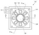
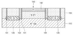
도 2a는 본 발명의 일 실시예에 따른 과도 전압 억제 소자(100)를 도시한 평면도이고, 도 2b 및 도 2c는 각각 도 2a의 2b-2b선 및 2c-2c선의 단면도이다.FIG. 2A is a plan view showing a transient
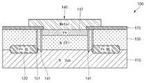
도 2a, 도 2b 및 도 2c에 도시된 바와 같이, 본 발명의 실시예에 따른 과도 전압 억제 소자(100)는 서브스트레이트(110)와, 매립층(120)과, 에피텍셜층(130)과, 중앙 소자 영역(140)과, 둘레 소자 영역(150)과, 상부 전극(140)을 포함할 수 있다.2A, 2B and 2C, a
서브스트레이트(110)는 제1도전형의 반도체일 수 있다. 즉, 서브스트레이트(110)는 대략 평평한 상면 및 대략 평평한 하면을 포함하는 판상일 수 있다. 서브스트레이트(110)는, 예를 들면, 한정하는 것은 아니지만, 진성 반도체에 5족 원소인 비소(As), 인(P) 또는 안티몬(Sb) 등의 불순물이 고고농도로 주입되어 형성된 N++형 반도체 기판일 수 있다. 여기서, 고고농도라 함은 후술할 제1도전형 영역(152)의 불순물 농도에 비해 상대적으로 농도가 크다는 의미이다.The
매립층(120)은 제2도전형의 반도체일 수 있다. 또한, 매립층(120)은 서브스트레이트(110)에 매립되고 수평 방향으로 상호간 이격된 형태일 수 있다. 실질적으로, 매립층(120)은 단면으로 보았을 때는 수평 방향으로 상호간 이격된 형태이나, 평면으로 보았을 때는 원형 또는 방사형으로 형성될 수 있다. 매립층(120)은, 예를 들면, 한정하는 것은 아니지만, 3족 원소인 갈륨(Ga), 인듐(In) 또는 붕소(B)등의 불순물과 같은 P+형 반도체를 이온 주입 또는 확산을 통해 서브스트레이트(110)에 형성할 수 있다.The buried
에피텍셜층(130)은 제1도전형의 반도체일 수 있다. 즉, 에피텍셜층(130)은 서브스트레이트(110) 및 한쌍의 매립층(120) 위에 N형의 반도체가 증착되어 형성될 수 있다. 여기서, 한쌍의 매립층(120)은 서브스트레이트(110)뿐만 아니라 에피텍셜층(130)의 내측으로 함께 확산된다.The
한편, 한쌍의 매립층(120) 사이의 영역인 에피텍셜층(130)으로부터 서브스트레이트(110)까지 중앙 격리 영역(141)이 형성되고, 또한 한쌍의 매립층(120)과 대응되는 에피텍셜층(130)으로부터 매립층(120)에까지 둘레 격리 영역(151)이 형성된다. 중앙 격리 영역(141) 및 둘레 격리 영역(151)은 각각 트렌치가 형성된 후, 트렌치에 절연체가 주입되어 형성될 수 있다. 여기서, 중앙 격리 영역(141)의 내측에는 중앙 소자 영역(140)이 형성되고, 둘레 격리 영역(151)의 내측에는 둘레 소자 영역(150)이 형성된다.A
중앙 소자 영역(140)은 한쌍의 매립층(120) 사이의 에피텍셜층(130)의 표면에 제2도전형의 웰 영역(142)이 형성되어 수직 방향으로 중앙 다이오드가 형성되도록 하여 이루어진다. 즉, 중앙의 에피텍셜층(130)의 표면으로부터 내부를 향하여 제2도전형의 웰 영역(142)이 형성된다. 보다 구체적으로, 중앙 격리 영역(141)의 내측으로서 한쌍의 매립층(120) 사이의 에피텍셜층(130) 표면으로부터 내측으로 고농도의 P+형 불순물을 이온 주입하여 웰 영역(142)이 형성될 수 있다. 이러한 웰 영역(142)의 수평 방향 폭은 중앙 격리 영역(141)의 내측 수평 방향 폭과 동일할 수 있다. 웰 영역(142)은 1차로 규소 산화막, 질소 산화막 등의 절연막(미도시)을 형성한 후, 3족 원소인 갈륨(Ga), 인듐(In) 또는 붕소(B) 등을 직접 이온주입 하거나 또는 열확산 공정을 이용함으로써, P+형인 제2도전형의 웰 영역(142)을 형성할 수 있다. 이러한 제2도전형의 웰 영역(142)과, 제1도전형의 에피텍셜층(130) 및 제1도전형의 서브스트레이트(110)에 의해 수직 방향으로 중앙 다이오드(즉, 정류 다이오드)가 형성되며, 이러한 구조에 의해 중앙 소자 영역(140)이 구비된다.The
둘레 소자 영역(150)은 한쌍의 매립층(120) 각각과 중첩된 에피텍셜층(130)의 표면에 제1도전형 영역(152)이 형성되어 수직 방향으로 정류 다이오드 및 제너 다이오드가 형성되도록 하여 이루어진다. 즉, 둘레의 에피텍셜층(130)의 표면으로부터 내부를 향하여 제1도전형 영역(152)이 형성된다. 보다 구체적으로, 둘레 격리 영역(151)의 내측으로서 한쌍의 매립층(120)과 각각 중첩하는 에피텍셜층(130)의 표면으로부터 내측으로 N+형 불순물을 이온 주입하여 제1도전형 영역(152)이 형성된다. 이러한 제1도전형 영역(152)의 수평 방향 폭은 둘레 격리 영역(151)의 내측 수평 방향 폭과 동일할 수 있다. 제1도전형 영역(152)은 규소 산화막, 질소 산화막 등의 절연막(도시하지 않음)을 형성한 후, 5족 원소인 비소(As), 인(P) 또는 안티몬(Sb) 등을 직접 이온주입 하거나 또는 열확산 공정을 이용함으로써, N+형의 고농도의 제1도전형 영역(152)을 형성할 수 있다. 여기서, 고농도라 함은 에피텍셜층(130)의 불순물 농도에 비해 상대적으로 농도가 크다는 의미이다.In the
이러한 제1도전형 영역(152)과, 제2도전형 매립층(120)에 의해 수직 방향의 정류 다이오드가 형성되고, 또한 제2도전형 매립층(120)과 제1도전형 서브스트레이트(110)에 의해 수직 방향의 제너 다이오드가 형성되며, 이러한 구조에 의해 둘레 소자 영역(150)이 구비된다.The rectifying diodes in the vertical direction are formed by the first
한편, 과도 전압 억제 소자(100)를 평면에서 보았을 때(도 2a 참조), 대략 원형의 중앙 소자 영역(140)(즉, 제2도전형의 웰 영역(142))을 중심으로 대략 직사각형의 둘레 소자 영역(150)(즉, 제1도전형 영역(152) 및/또는 매립층(120))이 방사상으로 배열될 수 있다.On the other hand, when the transient
또한, 과도 전압 억제 소자(100)를 단면에서 보았을 때(도 2b 참조)는, 중앙 소자 영역(140)을 중심으로 둘레 소자 영역(150)이 대칭되는 형태로 형성된다. 즉, 중앙 소자 영역(140)을 중심으로 좌측과 우측의 둘레 소자 영역(150)이 상호간 동일한 형태로 형성된다.When the transient
또한, 과도 전압 억제 소자(100)를 평면/단면에서 보았을 때, 중앙 소자 영역(140)을 중심으로 둘레 소자 영역(150)이 중앙 소자 영역(140)으로부터 멀어지는 수평 방향으로 일정 길이만큼 연장된 형태를 한다.When the transient
또한, 과도 전압 억제 소자(100)를 평면에서 보았을 때(도 2a 참조), 대략 원형의 중앙 소자 영역(140)은 대략 원형 링 모양의 중앙 격리 영역(141)에 의해 격리되고, 대략 직사각형의 둘레 소자 영역(150)은 대략 직사각 라인 모양의 둘레 격리 영역(151)에 의해 격리된다.2A), the substantially circular
특히, 둘레 소자 영역(150)(또는 제1도전형 영역(152) 및/또는 매립층(120))을 격리시키는 둘레 격리 영역(151)은 중앙 소자 영역(140)과 경계를 이루는 호 형태의 제1격리 라인(151a)과, 중앙 소자 영역(140)으로부터 방사상 외측으로 일정 길이 연장된 제2격리 라인(151b)과, 중앙 소자 영역(140)으로부터 방사상 외측으로 연장되며 제2격리 라인(151b)와 이격된 제3격리 라인(151c)과, 제2격리 라인(152b) 및 제3격리 라인(152c)의 단부를 연결하며 제1격리 라인(151a)과 이격된 제4격리 라인(151d)을 포함할 수 있다.In particular, the
여기서, 제1격리 라인(151a)의 길이에 비해 제4격리 라인(151d)의 길이가 더 길 수 있다. 즉, 둘레 소자 영역(150)(또는 제1도전형 영역(152) 및/또는 매립층(120))은 중앙 소자 영역(140)으로부터 멀어짐에 따라 점차 폭이 넓어질 수 있다.Here, the length of the
또한, 제1,4격리 라인(151a,151d)의 길이에 비해 상기 제2,3격리 라인(151b,151c)의 길이가 더 길 수 있다. 즉, 둘레 소자 영역(150)(또는 제1도전형 영역(152) 및/또는 매립층(120))은 중앙 소자 영역(140)으로부터 멀어짐에 따라 상대적으로 긴 대략 직사각 형태일 수 있다.Also, the lengths of the second and
여기서, 과도 전압 억제 소자(100)를 평면에서 보았을 때, 중앙 소자 영역(140)을 중심으로 매립층(120) 및 제1도전형 영역(152)이 방사상으로 배열되거나, 또는 과도 전압 억제 소자(100)를 평면에서 보았을 때, 중앙 소자 영역(140)을 중심으로 매립층(120)은 원형의 링 형태로 형성되고, 제1도전형 영역(152)은 분리되어 방사상으로 배열될 수 있다.Here, when the transient
또한, 도 2a 및 도 2b에 도시된 바와 같이, 방사상으로 배열된 둘레 소자 영역(150)의 사이에는 직접 에피텍셜층(130)이 개재될 수 있음으로써, 이부분을 통해서는 전류가 흐르지 않게 된다.In addition, as shown in FIGS. 2A and 2B, since the
한편, 상술한 중앙 소자 영역(140)(즉, 제2도전형의 웰 영역(142)) 및 둘레 소자 영역(150)(즉, 제1도전형 영역(152))에는 상부 전극(160)이 형성되고, 서브스트레이트(110)의 하면에는 하부 전극(미도시)이 형성된다. 물론, 중앙 격리 영역(141)과 둘레 격리 영역(151)의 사이에 절연막(170)이 개재되고, 또한 둘레 격리 영역(151)의 외측에도 절연막(170)이 형성됨으로써, 상부 전극(160)이 에피텍셜층(130)에 직접 콘택하지 않도록 되어 있다.The
이와 같이 하여, 본 발명의 다양한 실시예는 다이오드를 갖는 중앙 소자 영역(140)을 중심으로 정류 다이오드 및 제너 다이오드를 갖는 둘레 소자 영역(150)이 평면에서 보았을 때 방사상으로 배열되도록 형성함으로써, 둘레 소자 영역(150)의 면적은 증가시키지 않아 로우 캐패시턴스를 유지하면서도 전류 통로는 확장시켜 전류 특성(Ipp)을 향상시킬 수 있는 과도 전압 억제 소자(100)를 제공한다.Thus, in various embodiments of the present invention, the
도 3은 본 발명의 일 실시예에 따른 과도 전압 억제 소자(100)의 제조 방법을 도시한 순서도이다.3 is a flowchart showing a method of manufacturing the transient
도 3에 도시된 바와 같이 본 발명에 과도 전압 억제 소자(100)의 제조 방법은 서브스트레이트 준비 단계(S1)와, 매립층 형성 단계(S2)와, 에피텍셜층 형성 단계(S3)와, 격리 영역 형성 단계(S4)와, 웰 영역 형성 단계(S5)와, 제1도전형 영역 형성 단계(S6)와, 전극 형성 단계(S7)를 포함한다. 여기서, 웰 영역 형성 단계(S5)와 제1도전형 영역 형성 단계(S6)의 순서는 상호간 바뀔 수도 있다.3, the method for manufacturing the transient
도 4a 내지 도 4g는 본 발명의 일 실시예에 따른 과도 전압 억제 소자(100)의 제조 방법을 도시한 단면도이다. 여기서, 도 3을 함께 참조하여, 과도 전압 억제 소자(100)의 제조 방법을 설명한다.4A to 4G are cross-sectional views illustrating a method of manufacturing the transient
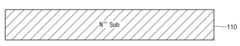
도 4a에 도시된 바와 같이, 서브스트레이트 준비 단계(S1)에서, 제1도전형의 서브스트레이트(110)가 준비된다. 서브스트레이트(110)는 상면 및 하면을 포함하는 판상의 형태로 이루어질 수 있다. 서브스트레이트(110)는, 일례로, 진성 반도체에 5족 원소인 비소(As), 인(P) 또는 안티몬(Sb) 등의 불순물이 고고농도로 주입되어 형성된 N++형 반도체 기판일 수 있다. 여기서, 고고농도라 함은 후술할 제1도전형 영역(152)의 불순물 농도에 비해 상대적으로 농도가 높다는 의미이다. 한편, 제1도전형의 서브스트레이트(110)는 진성 반도체에 3족 원소인 갈륨(Ga), 인듐(In) 또는 붕소(B)등의 불순물이 고농도로 주입된 P++형일 수도 있다. 다만, 본 발명에서는 상기 서브스트레이트(110)가 N++형으로 이루어지는 것으로 설명하도록 한다.As shown in FIG. 4A, in the substrate preparation step S1, a
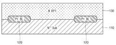
도 4b에 도시된 바와 같이, 매립층 형성 단계(S2)에서, 서브스트레이트(110)의 상면에 수평 방향으로 이격된 제2도전형의 매립층(120)이 형성된다. 여기서, 매립층(120)은 서브스트레이트(110)의 상면으로부터 내부를 향하여 일정 깊이로 형성된다. 또한, 매립층(120)은 상호간 일정 거리 이격될 수 있다.As shown in FIG. 4B, in the buried layer forming step S2, a buried
매립층(120)은 서브스트레이트(110)의 상면에 1차로 규소 산화막, 질소 산화막 등의 절연막(미도시)을 매립층(120)이 형성될 이외의 영역에 형성한 후, 3족 원소인 갈륨(Ga), 인듐(In) 또는 붕소(B)등의 불순물을 직접 이온주입 하거나 또는 열확산 공정을 이용하여 고농도 P+형인 매립층(120)을 형성할 수 있다.The buried
한편, 서브스트레이트(110)의 하면에는 하면 절연막이 형성될 수 있다. 상기 하면 절연막은 규소 산화막, 질소 산화막, 언도프트 폴리 실리콘(undoped poly silicon), PSG(Phospho-Silicate-Glass), BPSG(Boro-Phosphor-Silicate-Glass) 또는 이들의 등가물 중 선택된 어느 하나로 형성될 수 있으나, 이것으로 본 발명을 한정하는 것은 아니다. 하면 절연막은 고고농도의 제1도전형 서브스트레이트(110)의 오토도핑을 방지한다.On the other hand, a bottom insulating film may be formed on the bottom surface of the
도 4c에 도시된 바와 같이, 에피텍셜층 형성 단계(S3)에서, 서브스트레이트(110)의 상면에는 에피텍셜층(130)이 형성될 수 있다. 일례로, 600~2000℃의 고온에서 서브스트레이트(110)의 상면에 SiH4등의 가스와 5가 원소인 비소(As), 인(P) 또는 안티몬(Sb) 등이 포함된 가스를 저농도로 함께 흘려줌으로써, 상기 서브스트레이트(110) 및 매립층(120)의 표면에 N형의 에피텍셜층(130)이 증착되도록 할 수 있다. 이때, 에피텍셜층(130)이 매립층(120)의 표면에 증착되면서, 매립층(120)이 도핑 가스들에 의하여 에피텍셜층(130)으로 확산된 대략 타원형의 매립층(120)을 형성하게 된다.As shown in FIG. 4C, in the epitaxial layer forming step S3, the
도 4d에 도시된 바와 같이, 격리 영역 형성 단계(S4)에서, 중앙 격리 영역(141) 및 둘레 격리 영역(151)이 형성된다.4D, in the isolation region forming step S4, the
중앙 격리 영역(141)은 상호간 이격된 한쌍의 매립층(120) 사이의 에피텍셜층(130)에서 서브스트레이트(110)까지 트렌치가 형성되고, 이후 트렌치에 절연재가 충진되어 형성된다. 이러한 중앙 격리 영역(141)의 내측에 추후 중앙 소자 영역(140)이 형성된다.The
둘레 격리 영역(151)은 에피텍셜층(130) 및 그 하부의 매립층(120)까지 트렌치가 형성되고, 이후 트렌치에 절연재가 충진되어 형성된다. 이러한 둘레 격리 영역(151)의 내측에 추후 둘레 소자 영역(150)이 형성된다.The
여기서, 중앙 격리 영역(141) 및 둘레 격리 영역(151)은, 예를 들어, 1차로 트렌치의 위치를 확정하는 마스크(미도시) 부분만 남기고 노광되어 패턴(pattern)이 에피텍셜층(130) 위에 형성되고, 그런 다음, 마스크 개구부를 이용하여 반응성 이온 에칭(Ion etching) 또는 드라이 에칭(dry etching) 등을 통해 트렌치가 형성된다. 이후, 트렌치의 내부에 규소 산화막, 질소 산화막 등의 절연성 재료가 충진됨으로써, 중앙 격리 영역(141) 및 둘레 격리 영역(151)이 형성된다. 그러나, 본 발명에서 이러한 중앙 및 둘레 격리 영역(141,151)의 형성 방법이 한정되지 않으며, 여기에 기술되지 않은 다양한 방법이 가능하다.Here, the
도 4e에 도시된 바와 같이, 웰 영역 형성 단계(S5)에서, 에피텍셜층(130)의 표면으로부터 내부를 향하여 제2도전형의 웰 영역(142)이 형성된다. 보다 구체적으로, 중앙 격리 영역(141)의 내측으로서 한쌍의 매립층(120) 사이의 에피텍셜층(130) 표면으로부터 내측으로 이온 주입하여 웰 영역(142)이 형성된다. 이러한 웰 영역(142)의 수평 방향 폭은 중앙 격리 영역(141)의 내측 수평 방향 폭과 동일하다. 웰 영역(142)은 1차로 규소 산화막, 질소 산화막 등의 절연막(미도시)을 형성한 후, 3족 원소인 갈륨(Ga), 인듐(In) 또는 붕소(B) 등을 직접 이온주입 하거나 또는 열확산 공정을 이용함으로써 P+형인 제2도전형의 웰 영역(142)을 형성할 수 있다. 이러한 웰 영역(142)은 중앙 소자 영역(140)의 한 구성 요소가 된다.4E, in the well region formation step S5, the
도 4f에 도시된 바와 같이, 제1도전형 영역 형성 단계(S6)에서, 에피텍셜층(130)의 표면으로부터 내부를 향하여 제1도전형 영역(152)이 형성된다.As shown in FIG. 4F, in the first conductive type region forming step S6, the first
보다 구체적으로, 둘레 격리 영역(151)의 내측으로서 매립층(120) 위의 에피텍셜층(130)의 표면으로부터 내측으로 이온 주입하여 제1도전형 영역(152)이 형성된다. 이러한 제1도전형 영역(152)의 수평 방향 폭은 둘레 격리 영역(151)의 내측 수평 방향 폭과 동일하다. 이러한 제1도전형 영역(152)은 규소 산화막, 질소 산화막 등의 절연막(도시하지 않음)을 형성한 후, 5족 원소인 비소(As), 인(P) 또는 안티몬(Sb) 등을 직접 이온주입 하거나 또는 열확산 공정을 이용함으로써 N+형의 고농도의 제1도전형 영역(152)을 형성할 수 있다. 여기서, 고농도라 함은 에피텍셜층(130)의 불순물 농도에 비해 상대적으로 농도가 크다는 의미이다. 이러한 제1도전형 영역(152)은 둘레 소자 영역(150)의 한 구성 요소가 된다.More specifically, the first
도 4g에 도시된 바와 같이, 전극 형성 단계(S7)에서, 중앙 소자 영역(140) 및 둘레 소자 영역(150)의 상면에 상부 전극(160)이 형성되고, 서브스트레이트(110)의 하면에 하부 전극(미도시)이 형성된다. 이와 같이 하여 상부 전극(160)에 의해 중앙 소자 영역(140) 및 둘레 소자 영역(150)이 전기적으로 연결된다. 즉, 상부 전극(160)에 의해 중앙 소자 영역(140)의 제2도전형의 웰 영역(142)과 둘레 소자 영역(150)의 제1도전형 영역(152)이 상호간 전기적으로 연결된다.4G, the
여기서, 상부 전극(160) 및 하부 전극은 몰리브덴(Mo), 알루미늄(Al), 니켈(Ni) 및 금(Au) 또는 그 등가물 중 선택된 어느 하나를 순차 스퍼터링 또는 순차 도금하여 형성할 수 있으나, 이것으로 본 발명을 한정하는 것은 아니다.Here, the
또한, 중앙 소자 영역(140)과 둘레 소자 영역(150)의 사이, 그리고 둘레 소자 영역(150)의 외측에 절연막(170)이 형성될 수 있으며, 이는 규소 산화막, 질소 산화막, 언도프트 폴리 실리콘(undoped poly silicon), PSG(Phospho-Silicate-Glass), BPSG(Boro-Phosphor-Silicate-Glass) 또는 이들의 등가물 중 선택된 어느 하나로 형성될 수 있으나, 이것으로 본 발명을 한정하는 것은 아니다.An insulating
도 5는 본 발명의 일 실시예에 따른 과도 전압 억제 소자(100)의 등가 회로의 일례를 도시한 것이다.5 shows an example of an equivalent circuit of the transient
도 5에 도시된 바와 같이, 먼저 중앙 소자 영역(140) 중 제2도전형 웰 영역(142)과 그 하부의 제1도전형 에피텍셜층(130) 및 제1도전형 서브스트레이트(110)에 의해 정류 다이오드가 형성된다. 또한, 도 5에 도시된 바와 같이 둘레 소자 영역(150) 중 제1도전형 영역(152)과 제2도전형 매립층(120)에 의해 정류 다이오드가 형성되고, 또한 제2도전형 매립층(120)과 제1도전형 서브스트레이트(110)의 사이에 제너 다이오드가 형성된다. 여기서, 중앙의 정류 다이오드의 캐소드와 둘레의 정류 다이오드의 애노드가 상부 전극(160)에 의해 전기적으로 접속되고, 중앙의 정류 다이오드의 애노드와 둘레의 제너 다이오드의 애노드가 하부 전극에 의해 전기적으로 접속된다. 따라서, 이러한 다이오드 접속 구조에 의해 과도 전압 억제 소자(100)로서 동작하게 된다.5, the first conductive
여기서, 중앙의 다이오드를 포함하는 중앙 소자 영역은 1개가 형성된 것으로 볼 수 있고, 둘레의 상호간 직렬 연결된 정류 다이오드 및 제너 다이오드를 갖는 둘레 소자 영역은 8개로 형성된 것으로 볼 수 있다(도 2a 참조). 또한, 1개의 중앙 소자 영역을 중심으로 병렬로 그 둘레를 따라 방사상으로 8개의 둘레 소자 영역이 연결된 것으로 볼 수 있다.Here, it can be seen that one central element region including the central diode is formed, and the number of the peripheral element regions having the rectifier diodes and the zener diodes connected in series between the peripheries is eight (see FIG. 2A). Further, it can be seen that eight peripheral element regions are connected in a radial fashion around one central element region in parallel.
이와 같이 하여, 본 발명의 다양한 실시예는 다이오드를 갖는 중앙 소자 영역을 중심으로 정류 다이오드 및 제너 다이오드를 갖는 둘레 소자 영역이 평면에서 보았을 때 방사상으로 배열됨으로써, 둘레 소자 영역의 면적은 증가시키지 않아 로우 캐패시턴스를 유지하면서도 전류 통로는 확장시켜 전류(Ipp) 특성을 향상시킬 수 있는 과도 전압 억제 소자(100) 및 그 제조 방법을 제공하게 된다.Thus, the various embodiments of the present invention are arranged such that the peripheral element regions having the rectifying diodes and the zener diodes around the central element region having the diodes are arranged radially when viewed in plan, so that the area of the peripheral element region is not increased, The present invention provides a transient
일례로, 기존의 5V 0.5pF급 양방향 과도 전압 억제 소자의 경우 전류(Ipp)가 5A였으나, 상술한 구조를 채택한 5V 0.5pF급 양방향 과도 전압 억제 소자의 경우 전류(Ipp)가 6~6.5A로 증가함으로써, 본 발명의 실시예에 따른 과도 전압 억제 소자는 기존과 같은 로우 캐패시턴스를 가지면서도 전류 특성을 나타내는 Ipp는 대략 30% 증가함을 볼 수 있었다.For example, in the conventional 5V 0.5pF class bi-directional transient voltage suppressor, the current (Ipp) was 5A. However, in the case of the 5V 0.5pF class bi-directional transient voltage suppressor employing the above structure, It can be seen that the transient voltage suppressor according to the embodiment of the present invention has an Ipp which shows a current characteristic while having a low capacitance as in the prior art by about 30%.
이상에서 설명한 것은 본 발명에 따른 과도 전압 억제 소자 및 그 제조 방법을 실시하기 위한 하나의 실시예에 불과한 것으로서, 본 발명은 상기한 실시예에 한정되지 않고, 이하의 특허청구범위에서 청구하는 바와 같이 본 발명의 요지를 벗어남이 없이 당해 발명이 속하는 분야에서 통상의 지식을 가진 자라면 누구든지 다양한 변경 실시가 가능한 범위까지 본 발명의 기술적 정신이 있다고 할 것이다.It is to be understood that the present invention is not limited to the above-described embodiment, and various modifications may be made without departing from the scope of the present invention as set forth in the following claims It will be understood by those of ordinary skill in the art that various changes in form and details may be made therein without departing from the spirit and scope of the invention.
100; 본 발명의 실시예에 따른 과도 전압 억제 소자
110; 서브스트레이트120; 매립층
130; 에피텍셜층140; 중앙 소자 영역
141; 중앙 격리 영역142; 웰 영역
150; 둘레 소자 영역151; 둘레 격리 영역
152; 제1도전형 영역160; 상부 전극
170; 절연막100; The transient voltage suppressor < RTI ID = 0.0 >
110;
130; An
141; A
150; A
152; A first
170; Insulating film
Claims (12)
Translated fromKorean상기 서브스트레이트에 매립되고 수평 방향으로 이격된 한쌍의 제2도전형의 매립층;
상기 서브스트레이트 및 한쌍의 매립층 위에 형성된 제1도전형의 에피텍셜층;
상기 한쌍의 매립층 사이의 상기 에피텍셜층의 표면에 제2도전형의 웰 영역이 형성되어 수직 방향으로 중앙 다이오드가 형성되도록 하는 중앙 소자 영역; 및
상기 한쌍의 매립층 각각과 중첩된 상기 에피텍셜층의 표면에 제1도전형 영역이 형성되어 수직 방향으로 정류 다이오드 및 제너 다이오드가 형성되도록 하는 둘레 소자 영역을 포함하고,
평면에서 보았을 때 상기 중앙 소자 영역을 중심으로 상기 둘레 소자 영역은 방사상으로 배열된 것을 특징으로 하는 과도 전압 억제 소자.A substrate of a first conductivity type;
A pair of second conductive buried layers buried in the substrate and horizontally spaced apart;
An epitaxial layer of a first conductivity type formed over the substrate and the pair of buried layers;
A central element region in which a well region of a second conductivity type is formed on a surface of the epitaxial layer between the pair of buried layers to form a center diode in a vertical direction; And
And a peripheral element region in which a first conductive type region is formed on a surface of the epitaxial layer superimposed on each of the pair of buried layers to form a rectifying diode and a zener diode in a vertical direction,
Wherein the peripheral element region is arranged radially with respect to the central element region when viewed in plan.
상기 중앙 소자 영역을 중심으로 상기 둘레 소자 영역이 대칭되는 형태로 형성된 것을 특징으로 하는 과도 전압 억제 소자.The method according to claim 1,
Wherein the peripheral element region is formed symmetrically with respect to the central element region.
상기 중앙 소자 영역을 중심으로 상기 둘레 소자 영역이 상기 중앙 소자 영역으로부터 멀어지는 수평 방향으로 연장된 것을 특징으로 하는 과도 전압 억제 소자.The method according to claim 1,
And the peripheral element region extends in a horizontal direction away from the central element region, with the center element region being the center.
평면에서 보았을 때 상기 둘레 소자 영역은
상기 중앙 소자 영역과 경계를 이루는 호 형태의 제1격리 라인;
상기 중앙 소자 영역으로부터 방사상 외측으로 연장된 제2격리 라인;
상기 중앙 소자 영역으로부터 방사상 외측으로 연장되며 상기 제2격리 라인와 이격된 제3격리 라인; 및
상기 제1격리 라인의 반대 방향인 상기 제2격리 라인 및 제3격리 라인의 단부를 연결하는 제4격리 라인를 포함함을 특징으로 하는 과도 전압 억제 소자.The method according to claim 1,
When viewed in plan, the peripheral element region
A first isolation line in the form of an arc bordering the central element region;
A second isolation line extending radially outwardly from the central element region;
A third isolation line extending radially outward from the central element region and spaced apart from the second isolation line; And
And a fourth isolation line connecting the ends of the second isolation line and the third isolation line opposite to the first isolation line.
상기 제1격리 라인의 길이에 비해 상기 제4격리 라인의 길이가 더 긴 것을 특징으로 하는 과도 전압 억제 소자.5. The method of claim 4,
Wherein a length of the fourth isolation line is longer than a length of the first isolation line.
상기 제1,4격리 라인의 길이에 비해 상기 제2,3격리 라인의 길이가 더 긴 것을 특징으로 하는 과도 전압 억제 소자.5. The method of claim 4,
Wherein a length of the second and third isolation lines is longer than a length of the first and fourth isolation lines.
상기 방사상으로 배열된 둘레 소자 영역의 사이에는 상기 에피텍셜층이 개재된 것을 특징으로 하는 과도 전압 억제 소자.The method according to claim 1,
And wherein the epitaxial layer is interposed between the peripheral element regions arranged in the radial direction.
평면에서 보았을 때 상기 중앙 소자 영역을 중심으로 상기 매립층 및 상기 제1도전형 영역이 방사상으로 배열된 것을 특징으로 하는 과도 전압 억제 소자.The method according to claim 1,
Wherein said buried layer and said first conductivity type region are arranged radially about said central element region when viewed in plan.
평면에서 보았을 때 상기 중앙 소자 영역을 중심으로 상기 매립층은 원형으로 형성되고, 상기 제1도전형 영역은 방사상으로 배열된 것을 특징으로 하는 과도 전압 억제 소자.The method according to claim 1,
Wherein said buried layer is formed in a circular shape with respect to said central element region when viewed in plan, and said first conductivity type region is arranged radially.
상기 서브스트레이트에 수평 방향으로 이격된 한쌍의 제2도전형의 매립층을 형성하는 단계;
상기 서브스트레이트 및 매립층 위에 제1도전형의 에피텍셜층을 형성하는 단계;
상기 한쌍의 매립층 사이의 상기 에피텍셜층의 표면에 제2도전형의 웰 영역을 형성하여 수직 방향으로 중앙 다이오드가 형성되도록 하는 중앙 소자 영역 형성 단계; 및
상기 한쌍의 매립층 각각과 중첩된 상기 에피텍셜층의 표면에 제1도전형 영역을 형성하여 수직 방향으로 정류 다이오드 및 제너 다이오드가 형성되도록 하는 둘레 소자 영역 형성 단계를 포함하고,
평면에서 보았을 때 상기 중앙 소자 영역을 중심으로 상기 둘레 소자 영역은 방사상으로 배열된 것을 특징으로 하는 과도 전압 억제 소자의 제조 방법.Preparing a substrate of a first conductivity type;
Forming a pair of horizontally spaced second conductive buried layers in the substrate;
Forming an epitaxial layer of a first conductivity type over the substrate and the buried layer;
Forming a central diode region in a vertical direction by forming a well region of a second conductivity type on the surface of the epitaxial layer between the pair of the buried layers; And
And forming a rectifying diode and a zener diode in a vertical direction by forming a first conductive type region on a surface of the epitaxial layer overlapped with each of the pair of buried layers,
Wherein the peripheral element region is arranged radially with respect to the central element region when viewed in plan.
평면에서 보았을 때 상기 중앙 소자 영역을 중심으로 상기 매립층 및 상기 제1도전형 영역이 방사상으로 배열된 것을 특징으로 하는 과도 전압 억제 소자의 제조 방법.11. The method of claim 10,
Wherein the buried layer and the first conductive type region are arranged radially with respect to the central element region when viewed in plan.
평면에서 보았을 때 상기 중앙 소자 영역을 중심으로 상기 매립층은 원형으로 형성되고, 상기 제1도전형 영역은 방사상으로 배열된 것을 특징으로 하는 과도 전압 억제 소자의 제조 방법.11. The method of claim 10,
Wherein the buried layer is formed in a circular shape with respect to the central element region when viewed in a plane, and the first conductive type region is arranged radially.
Priority Applications (1)
| Application Number | Priority Date | Filing Date | Title |
|---|---|---|---|
| KR1020170010686AKR101850851B1 (en) | 2017-01-23 | 2017-01-23 | Transient voltage suppressor and manufacturing method thereof |
Applications Claiming Priority (1)
| Application Number | Priority Date | Filing Date | Title |
|---|---|---|---|
| KR1020170010686AKR101850851B1 (en) | 2017-01-23 | 2017-01-23 | Transient voltage suppressor and manufacturing method thereof |
Publications (1)
| Publication Number | Publication Date |
|---|---|
| KR101850851B1true KR101850851B1 (en) | 2018-04-23 |
Family
ID=62089015
Family Applications (1)
| Application Number | Title | Priority Date | Filing Date |
|---|---|---|---|
| KR1020170010686AActiveKR101850851B1 (en) | 2017-01-23 | 2017-01-23 | Transient voltage suppressor and manufacturing method thereof |
Country Status (1)
| Country | Link |
|---|---|
| KR (1) | KR101850851B1 (en) |
Cited By (1)
| Publication number | Priority date | Publication date | Assignee | Title |
|---|---|---|---|---|
| CN111180337A (en)* | 2019-12-30 | 2020-05-19 | 上海芯导电子科技有限公司 | One-way surge protection device and manufacturing method |
Citations (4)
| Publication number | Priority date | Publication date | Assignee | Title |
|---|---|---|---|---|
| US20150162743A1 (en) | 2013-12-11 | 2015-06-11 | General Electric Company | Method and system for over-voltage protection using transient voltage suppression devices |
| KR101570217B1 (en) | 2014-07-09 | 2015-11-18 | 주식회사 케이이씨 | transient voltage suppressor and manufacturing method thereof |
| KR20160086691A (en)* | 2015-01-12 | 2016-07-20 | 주식회사 케이이씨 | Transient voltage suppressor and manufacturing method thereof |
| KR101686569B1 (en) | 2015-06-18 | 2016-12-14 | 주식회사 케이이씨 | Transient Voltage Suppressor and Manufacturing Method thereof |
- 2017
- 2017-01-23KRKR1020170010686Apatent/KR101850851B1/enactiveActive
Patent Citations (4)
| Publication number | Priority date | Publication date | Assignee | Title |
|---|---|---|---|---|
| US20150162743A1 (en) | 2013-12-11 | 2015-06-11 | General Electric Company | Method and system for over-voltage protection using transient voltage suppression devices |
| KR101570217B1 (en) | 2014-07-09 | 2015-11-18 | 주식회사 케이이씨 | transient voltage suppressor and manufacturing method thereof |
| KR20160086691A (en)* | 2015-01-12 | 2016-07-20 | 주식회사 케이이씨 | Transient voltage suppressor and manufacturing method thereof |
| KR101686569B1 (en) | 2015-06-18 | 2016-12-14 | 주식회사 케이이씨 | Transient Voltage Suppressor and Manufacturing Method thereof |
Cited By (1)
| Publication number | Priority date | Publication date | Assignee | Title |
|---|---|---|---|---|
| CN111180337A (en)* | 2019-12-30 | 2020-05-19 | 上海芯导电子科技有限公司 | One-way surge protection device and manufacturing method |
Similar Documents
| Publication | Publication Date | Title |
|---|---|---|
| KR101414005B1 (en) | Transient voltage suppressor and its manufacturing method | |
| US8198703B2 (en) | Zener diode with reduced substrate current | |
| KR101570217B1 (en) | transient voltage suppressor and manufacturing method thereof | |
| KR20200019096A (en) | Semiconductor device | |
| KR100952267B1 (en) | Transient Voltage Suppression Element and Manufacturing Method Thereof | |
| KR101686569B1 (en) | Transient Voltage Suppressor and Manufacturing Method thereof | |
| US7859010B2 (en) | Bi-directional semiconductor ESD protection device | |
| KR101731587B1 (en) | Transient voltage suppressor and manufacturing method thereof | |
| KR101850851B1 (en) | Transient voltage suppressor and manufacturing method thereof | |
| KR101779588B1 (en) | Transient voltage suppressor and manufacturing method thereof | |
| KR101621145B1 (en) | Transient voltage suppressor and Integrated Circuit using the Same | |
| KR102171860B1 (en) | Uni-directional Transient Voltage Suppressor Having Snap-Back structure and manufacturing method thereof | |
| KR101893673B1 (en) | Transient voltage suppressor and manufacturing method thereof | |
| KR101686568B1 (en) | Transient Voltage Suppressor and Manufacturing Method thereof | |
| KR100945626B1 (en) | Transient voltage suppressor | |
| KR102712906B1 (en) | Asymmetric transient voltage suppressor device and methods for formation | |
| KR101607207B1 (en) | Transient voltage suppressor and manufacturing method thereof | |
| KR102171862B1 (en) | Uni-directional Transient Voltage Suppressor and manufacturing method thereof | |
| KR102187243B1 (en) | Uni-directional Transient Voltage Suppressor and manufacturing method thereof | |
| CN103178121B (en) | Pin diode and manufacturing method thereof | |
| KR102171861B1 (en) | Transient voltage suppression device and manufacturing method thereof | |
| KR102187242B1 (en) | Transient voltage suppression device and manufacturing method thereof | |
| KR101955098B1 (en) | Transient voltage suppressor and manufacturing method thereof | |
| KR102103195B1 (en) | Bidirectional Low Clamping Transient Voltage Suppression Device Using Trigger Type Schokley Diodes and manufacturing method thereof | |
| CN110504326A (en) | Schottky diode |
Legal Events
| Date | Code | Title | Description |
|---|---|---|---|
| PA0109 | Patent application | Patent event code:PA01091R01D Comment text:Patent Application Patent event date:20170123 | |
| PA0201 | Request for examination | ||
| E701 | Decision to grant or registration of patent right | ||
| PE0701 | Decision of registration | Patent event code:PE07011S01D Comment text:Decision to Grant Registration Patent event date:20180320 | |
| GRNT | Written decision to grant | ||
| PR0701 | Registration of establishment | Comment text:Registration of Establishment Patent event date:20180416 Patent event code:PR07011E01D | |
| PR1002 | Payment of registration fee | Payment date:20180417 End annual number:3 Start annual number:1 | |
| PG1601 | Publication of registration | ||
| PR1001 | Payment of annual fee | Payment date:20210310 Start annual number:4 End annual number:4 | |
| PR1001 | Payment of annual fee | Payment date:20230110 Start annual number:6 End annual number:6 | |
| PR1001 | Payment of annual fee | Payment date:20250203 Start annual number:8 End annual number:8 |