KR101850428B1 - Light emitting module, display device including the same - Google Patents
Light emitting module, display device including the sameDownload PDFInfo
- Publication number
- KR101850428B1 KR101850428B1KR1020100118022AKR20100118022AKR101850428B1KR 101850428 B1KR101850428 B1KR 101850428B1KR 1020100118022 AKR1020100118022 AKR 1020100118022AKR 20100118022 AKR20100118022 AKR 20100118022AKR 101850428 B1KR101850428 B1KR 101850428B1
- Authority
- KR
- South Korea
- Prior art keywords
- light
- light source
- sheet
- lens
- source module
- Prior art date
- Legal status (The legal status is an assumption and is not a legal conclusion. Google has not performed a legal analysis and makes no representation as to the accuracy of the status listed.)
- Expired - Fee Related
Links
Images


Classifications
- G—PHYSICS
- G02—OPTICS
- G02F—OPTICAL DEVICES OR ARRANGEMENTS FOR THE CONTROL OF LIGHT BY MODIFICATION OF THE OPTICAL PROPERTIES OF THE MEDIA OF THE ELEMENTS INVOLVED THEREIN; NON-LINEAR OPTICS; FREQUENCY-CHANGING OF LIGHT; OPTICAL LOGIC ELEMENTS; OPTICAL ANALOGUE/DIGITAL CONVERTERS
- G02F1/00—Devices or arrangements for the control of the intensity, colour, phase, polarisation or direction of light arriving from an independent light source, e.g. switching, gating or modulating; Non-linear optics
- G02F1/01—Devices or arrangements for the control of the intensity, colour, phase, polarisation or direction of light arriving from an independent light source, e.g. switching, gating or modulating; Non-linear optics for the control of the intensity, phase, polarisation or colour
- G02F1/13—Devices or arrangements for the control of the intensity, colour, phase, polarisation or direction of light arriving from an independent light source, e.g. switching, gating or modulating; Non-linear optics for the control of the intensity, phase, polarisation or colour based on liquid crystals, e.g. single liquid crystal display cells
- G02F1/133—Constructional arrangements; Operation of liquid crystal cells; Circuit arrangements
- G02F1/1333—Constructional arrangements; Manufacturing methods
- G02F1/1335—Structural association of cells with optical devices, e.g. polarisers or reflectors
- G02F1/1336—Illuminating devices
- G—PHYSICS
- G02—OPTICS
- G02B—OPTICAL ELEMENTS, SYSTEMS OR APPARATUS
- G02B26/00—Optical devices or arrangements for the control of light using movable or deformable optical elements
- G02B26/02—Optical devices or arrangements for the control of light using movable or deformable optical elements for controlling the intensity of light
- G—PHYSICS
- G02—OPTICS
- G02B—OPTICAL ELEMENTS, SYSTEMS OR APPARATUS
- G02B6/00—Light guides; Structural details of arrangements comprising light guides and other optical elements, e.g. couplings
- G02B6/0001—Light guides; Structural details of arrangements comprising light guides and other optical elements, e.g. couplings specially adapted for lighting devices or systems
- G02B6/0011—Light guides; Structural details of arrangements comprising light guides and other optical elements, e.g. couplings specially adapted for lighting devices or systems the light guides being planar or of plate-like form
- G02B6/0033—Means for improving the coupling-out of light from the light guide
- G02B6/005—Means for improving the coupling-out of light from the light guide provided by one optical element, or plurality thereof, placed on the light output side of the light guide
- G02B6/0053—Prismatic sheet or layer; Brightness enhancement element, sheet or layer
- G—PHYSICS
- G02—OPTICS
- G02B—OPTICAL ELEMENTS, SYSTEMS OR APPARATUS
- G02B6/00—Light guides; Structural details of arrangements comprising light guides and other optical elements, e.g. couplings
- G02B6/0001—Light guides; Structural details of arrangements comprising light guides and other optical elements, e.g. couplings specially adapted for lighting devices or systems
- G02B6/0011—Light guides; Structural details of arrangements comprising light guides and other optical elements, e.g. couplings specially adapted for lighting devices or systems the light guides being planar or of plate-like form
- G02B6/0033—Means for improving the coupling-out of light from the light guide
- G02B6/005—Means for improving the coupling-out of light from the light guide provided by one optical element, or plurality thereof, placed on the light output side of the light guide
- G02B6/0055—Reflecting element, sheet or layer
- G—PHYSICS
- G02—OPTICS
- G02B—OPTICAL ELEMENTS, SYSTEMS OR APPARATUS
- G02B6/00—Light guides; Structural details of arrangements comprising light guides and other optical elements, e.g. couplings
- G02B6/0001—Light guides; Structural details of arrangements comprising light guides and other optical elements, e.g. couplings specially adapted for lighting devices or systems
- G02B6/0011—Light guides; Structural details of arrangements comprising light guides and other optical elements, e.g. couplings specially adapted for lighting devices or systems the light guides being planar or of plate-like form
- G02B6/0081—Mechanical or electrical aspects of the light guide and light source in the lighting device peculiar to the adaptation to planar light guides, e.g. concerning packaging
- G02B6/0086—Positioning aspects
- G02B6/0088—Positioning aspects of the light guide or other optical sheets in the package
- G—PHYSICS
- G02—OPTICS
- G02F—OPTICAL DEVICES OR ARRANGEMENTS FOR THE CONTROL OF LIGHT BY MODIFICATION OF THE OPTICAL PROPERTIES OF THE MEDIA OF THE ELEMENTS INVOLVED THEREIN; NON-LINEAR OPTICS; FREQUENCY-CHANGING OF LIGHT; OPTICAL LOGIC ELEMENTS; OPTICAL ANALOGUE/DIGITAL CONVERTERS
- G02F1/00—Devices or arrangements for the control of the intensity, colour, phase, polarisation or direction of light arriving from an independent light source, e.g. switching, gating or modulating; Non-linear optics
- G02F1/01—Devices or arrangements for the control of the intensity, colour, phase, polarisation or direction of light arriving from an independent light source, e.g. switching, gating or modulating; Non-linear optics for the control of the intensity, phase, polarisation or colour
- G02F1/13—Devices or arrangements for the control of the intensity, colour, phase, polarisation or direction of light arriving from an independent light source, e.g. switching, gating or modulating; Non-linear optics for the control of the intensity, phase, polarisation or colour based on liquid crystals, e.g. single liquid crystal display cells
- G02F1/133—Constructional arrangements; Operation of liquid crystal cells; Circuit arrangements
- G02F1/1333—Constructional arrangements; Manufacturing methods
- G02F1/1334—Constructional arrangements; Manufacturing methods based on polymer dispersed liquid crystals, e.g. microencapsulated liquid crystals
- G—PHYSICS
- G02—OPTICS
- G02F—OPTICAL DEVICES OR ARRANGEMENTS FOR THE CONTROL OF LIGHT BY MODIFICATION OF THE OPTICAL PROPERTIES OF THE MEDIA OF THE ELEMENTS INVOLVED THEREIN; NON-LINEAR OPTICS; FREQUENCY-CHANGING OF LIGHT; OPTICAL LOGIC ELEMENTS; OPTICAL ANALOGUE/DIGITAL CONVERTERS
- G02F1/00—Devices or arrangements for the control of the intensity, colour, phase, polarisation or direction of light arriving from an independent light source, e.g. switching, gating or modulating; Non-linear optics
- G02F1/01—Devices or arrangements for the control of the intensity, colour, phase, polarisation or direction of light arriving from an independent light source, e.g. switching, gating or modulating; Non-linear optics for the control of the intensity, phase, polarisation or colour
- G02F1/13—Devices or arrangements for the control of the intensity, colour, phase, polarisation or direction of light arriving from an independent light source, e.g. switching, gating or modulating; Non-linear optics for the control of the intensity, phase, polarisation or colour based on liquid crystals, e.g. single liquid crystal display cells
- G02F1/133—Constructional arrangements; Operation of liquid crystal cells; Circuit arrangements
- G02F1/1333—Constructional arrangements; Manufacturing methods
- G02F1/1335—Structural association of cells with optical devices, e.g. polarisers or reflectors
- G02F1/1336—Illuminating devices
- G02F1/133602—Direct backlight
- G02F1/133606—Direct backlight including a specially adapted diffusing, scattering or light controlling members
- G—PHYSICS
- G02—OPTICS
- G02F—OPTICAL DEVICES OR ARRANGEMENTS FOR THE CONTROL OF LIGHT BY MODIFICATION OF THE OPTICAL PROPERTIES OF THE MEDIA OF THE ELEMENTS INVOLVED THEREIN; NON-LINEAR OPTICS; FREQUENCY-CHANGING OF LIGHT; OPTICAL LOGIC ELEMENTS; OPTICAL ANALOGUE/DIGITAL CONVERTERS
- G02F1/00—Devices or arrangements for the control of the intensity, colour, phase, polarisation or direction of light arriving from an independent light source, e.g. switching, gating or modulating; Non-linear optics
- G02F1/01—Devices or arrangements for the control of the intensity, colour, phase, polarisation or direction of light arriving from an independent light source, e.g. switching, gating or modulating; Non-linear optics for the control of the intensity, phase, polarisation or colour
- G02F1/13—Devices or arrangements for the control of the intensity, colour, phase, polarisation or direction of light arriving from an independent light source, e.g. switching, gating or modulating; Non-linear optics for the control of the intensity, phase, polarisation or colour based on liquid crystals, e.g. single liquid crystal display cells
- G02F1/133—Constructional arrangements; Operation of liquid crystal cells; Circuit arrangements
- G02F1/1333—Constructional arrangements; Manufacturing methods
- G02F1/1335—Structural association of cells with optical devices, e.g. polarisers or reflectors
- G02F1/1336—Illuminating devices
- G02F1/133602—Direct backlight
- G02F1/133611—Direct backlight including means for improving the brightness uniformity
Landscapes
- Physics & Mathematics (AREA)
- General Physics & Mathematics (AREA)
- Optics & Photonics (AREA)
- Nonlinear Science (AREA)
- Chemical & Material Sciences (AREA)
- Mathematical Physics (AREA)
- Crystallography & Structural Chemistry (AREA)
- Dispersion Chemistry (AREA)
- Planar Illumination Modules (AREA)
Abstract
Translated fromKoreanDescription
Translated fromKorean실시예는 발광소자를 포함하는 광원 모듈과 이를 포함하는 표시장치에 관한 것이다.Embodiments relate to a light source module including a light emitting element and a display device including the light source module.
반도체의 3-5족 또는 2-6족 화합물 반도체 물질을 이용한 발광다이오드(Lighit Emitting Diode; LED)나 레이저 다이오드(Laser Diode; LD)와 같은 발광 소자는 박막 성장 기술 및 소자 재료의 개발로 적색, 녹색, 청색 및 자외선 등 다양한 색을 구현할 수 있으며, 형광 물질을 이용하거나 색을 조합함으로써 효율이 좋은 백색 광선도 구현이 가능하며, 형광등, 백열등 등 기존의 광원에 비해 저소비전력, 반영구적인 수명, 빠른 응답속도, 안전성, 환경친화성의 장점을 가진다.BACKGROUND ART Light emitting devices such as a light emitting diode (LED) or a laser diode (LD) using semiconductor materials of Group 3-5 or 2-6 group semiconductors have been developed with thin film growth technology and device materials, Green, blue, and ultraviolet rays. By using fluorescent materials or combining colors, it is possible to realize white light rays with high efficiency. Also, compared to conventional light sources such as fluorescent lamps and incandescent lamps, low power consumption, It has the advantages of response speed, safety, and environmental friendliness.
따라서, 광 통신 수단의 송신 모듈, LCD(Liquid Crystal Display) 표시 장치의 백라이트를 구성하는 냉음극관(CCFL: Cold Cathode Fluorescence Lamp)을 대체하는 발광 다이오드 백라이트, 형광등이나 백열 전구를 대체할 수 있는 백색 발광 다이오드 조명 장치, 자동차 헤드 라이트 및 신호등에까지 응용이 확대되고 있다.Therefore, a transmission module of the optical communication means, a light emitting diode backlight replacing a cold cathode fluorescent lamp (CCFL) constituting a backlight of an LCD (Liquid Crystal Display) display device, a white light emitting element capable of replacing a fluorescent lamp or an incandescent lamp Diode lighting, automotive headlights, and traffic lights.
상기 발광소자는 직하형 또는 에지(edge)형 광원으로 백라이트 유닛에 구비되어, 표시장치에 사용되고 있다.The light emitting device is provided in a backlight unit as a direct-type or edge-type light source, and is used in a display device.
실시예는 백라이트 유닛에서 투사되는 광 분포를 고르게 하고자 하는 것이다.The embodiment attempts to even out the light distribution projected from the backlight unit.
실시예는 발광소자 패키지 어레이가 배치된 회로기판과, 상기 발광소자 패키지에서 방출되는 빛을 전달하고 상기 빛의 입사각이 임계각 이상인 제1 면과 임계각 미만인 제2 면이 각각 적어도 1개씩 구비된 렌즈를 포함하는 광원 모듈; 상기 광원 모듈에서 전달된 빛을 하기의 광학시트로 전달하는 반사시트; 및 상기 렌즈와 상기 반사시트로부터 전달된 빛을 투사하는 광학시트를 포함하는 백라이트 유닛을 제공한다.The present invention provides a light emitting device package comprising a circuit board on which a light emitting device package array is disposed, a lens having at least one first surface, which transmits light emitted from the light emitting device package and has a light incidence angle of more than a critical angle, A light source module including the light source module; A reflective sheet for transmitting light transmitted from the light source module to an optical sheet; And an optical sheet that projects the light transmitted from the lens and the reflective sheet.
여기서, 상기 렌즈는 굴절률이 1 이상인 고분자 물질일 수 있다.Here, the lens may be a high molecular material having a refractive index of 1 or more.
그리고, 상기 렌즈는 상기 제1 면과 제2 면이 적어도 2회 반복하여 배치될 수 있다.In addition, the lens may be arranged such that the first surface and the second surface are repeated at least twice.
그리고, 상기 회로기판은 상기 렌즈 상에 구비된 홈에 삽입되어 고정될 수 있다.The circuit board may be inserted into a groove provided on the lens and fixed.
그리고, 상기 홈은, 상기 회로기판이 상기 광학시트에 대하여 예각 또는 둔각을 이루도록 형성될 수 있다.The grooves may be formed such that the circuit board has an acute angle or an obtuse angle with respect to the optical sheet.
그리고, 상기 반사시트는 상기 광학시트에 대하여 기울어져 배치될 수 있다.The reflective sheet may be disposed to be inclined with respect to the optical sheet.
그리고, 상기 반사시트는 휘어지며 배치될 수 있다.The reflective sheet may be bent and disposed.
그리고, 상기 광학시트의 일부분 상에 구비되고, 상기 빛을 상기 반사시트로 반사하는 광반사층을 더 포함할 수 있다.The optical sheet may further include a light reflection layer provided on a part of the optical sheet and reflecting the light to the reflection sheet.
그리고, 상기 광반사층은 상기 광원 모듈으로부터 멀어질수록 밀도가 감소할수 있다.The density of the light reflecting layer may decrease as the distance from the light source module increases.
그리고, 상기 광반사층은 복수 개의 층으로 이루어지고, 상기 층은 상기 광원 모듈으로부터 멀어질수록 면적이 감소할 수 있다.In addition, the light reflecting layer may be formed of a plurality of layers, and the area may be reduced as the layer is further away from the light source module.
그리고, 상기 광반사층은 복수 개의 층으로 이루어지고, 상기 층은 상기 광원으로부터 멀어질수록 서로 멀리 이격될 수 있다.The light reflection layer may include a plurality of layers, and the layers may be spaced apart from each other as the layers are farther from the light source.
그리고, 상기 광학시트의 일부분 상에 구비되고, 상기 빛을 상기 반사시트로 산란시키는 광산란층을 더 포함할 수 있다.The optical sheet may further include a light scattering layer disposed on a part of the optical sheet and scattering the light to the reflection sheet.
그리고, 상기 광산란층은, TiO2 또는 Al2O3로 이루어질 수 있다.The light scattering layer may be made of TiO2 or Al2 O3 .
그리고, 상기 광산란층은 상기 광원 모듈으로부터 멀어질수록 밀도가 감소할 수 있다.The density of the light scattering layer may decrease as the distance from the light source module increases.
그리고, 상기 광산란층은 복수 개의 층으로 이루어지고, 상기 층은 상기 광원 모듈으로부터 멀어질수록 면적이 감소할 수 있다.The light scattering layer is formed of a plurality of layers, and the area of the light scattering layer may decrease as the layer is further away from the light source module.
또한, 상기 광산란층은 복수 개의 층으로 이루어지고, 상기 층은 상기 광원으로부터 멀어질수록 서로 멀리 이격될 수 있다.In addition, the light scattering layer may comprise a plurality of layers, and the layers may be spaced apart from each other as they are farther from the light source.
다른 실시예는 발광소자 패키지 어레이가 고정된 회로기판; 및 상기 발광소자 패키지에서 방출되는 빛을 전달하고, 상기 빛의 입사각이 임계각 이상인 제1 면과 임계각 미만인 제2 면이 각각 적어도 1개씩 구비된 렌즈를 포함하는 광원 모듈을 제공한다.Another embodiment includes a circuit board on which a light emitting device package array is fixed; And a lens that transmits light emitted from the light emitting device package and includes at least one first surface having a light incidence angle of at least a critical angle and at least one second surface having a critical angle less than the critical angle.
여기서, 상기 렌즈는 굴절률이 1 이상인 고분자 물질로 이루어지고, 상기 제1 면과 제2 면이 적어도 2회 반복하여 배치될 수 있다.Here, the lens may be made of a polymer material having a refractive index of at least 1, and the first surface and the second surface may be repeatedly arranged at least twice.
그리고, 상기 회로기판은 상기 렌즈 상에 구비된 홈에 삽입되어 고정되고, 상기 홈은 상기 회로기판이 상기 광학시트에 대하여 예각 또는 둔각을 이루도록 형성될 수 있다.The circuit board is inserted and fixed in a groove provided on the lens, and the groove may be formed such that the circuit board has an acute angle or an obtuse angle with respect to the optical sheet.
또 다른 실시예는 실시예는 발광소자 패키지 어레이가 고정된 회로기판과, 상기 발광소자 패키지에서 방출되는 빛을 전달하고 상기 빛의 입사각이 임계각 이상인 제1 면과 임계각 미만인 제2 면이 각각 적어도 1개씩 구비된 렌즈를 포함하는 광원 모듈, 상기 광원 모듈에서 전달된 빛을 하기의 광학시트로 전달하는 반사시트, 및 상기 렌즈와 상기 광학시트로부터 전달된 빛을 투사하는 광학시트를 포함하는 백라이트 유닛; 및 상기 백라이트 유닛 상에 상에 배치되고, 상기 빛에 의하여 화상을 구현하는 패널을 포함하는 표시장치를 제공한다.According to another embodiment of the present invention, there is provided a light emitting device package comprising: a circuit board on which a light emitting device package array is fixed; a first surface that transmits light emitted from the light emitting device package and has an incident angle of light greater than a critical angle, A backlight unit including a light source module including a plurality of lenses, a reflective sheet for transmitting light transmitted from the light source module to the optical sheet, and an optical sheet for projecting light transmitted from the optical sheet; And a panel disposed on the backlight unit and including a panel for realizing an image by the light.
실시예에 따른 백라이트 유닛은 광원 모듈에서 방출된 빛이 광학시트 전체로 고르게 투사되어, 패널에 전달되는 빛의 분포를 고르게 할 수 있다.The backlight unit according to the embodiment can uniformly distribute the light transmitted from the light source module to the entire optical sheet.
도 1은 실시예에 따른 표시장치의 분해 사시도이고,
도 2a는 도 1의 백라이트 모듈의 단면도이고,
도 2b는 도 2a의 A부분의 확대도이고,
도 3a 내지 도 3c는 도 2a의 광원 모듈의 실시예들의 단면도이고,
도 4a는 도 2a의 백라이트 유닛의 광분포를 나타낸 도면이고,
도 4b는 종래의 백라이트 유닛의 광분포를 나타낸 도면이고,
도 5a 내지 도 5f는 백라이트 유닛의 다른 실시예들을 나타낸 도면이고,
도 6a 및 도 6b는 백라이트 유닛의 또 다른 실시예들을 나타낸 도면이다.1 is an exploded perspective view of a display device according to an embodiment,
Figure 2a is a cross-sectional view of the backlight module of Figure 1,
FIG. 2B is an enlarged view of a portion A in FIG. 2A,
3A to 3C are sectional views of embodiments of the light source module of FIG. 2A,
FIG. 4A is a diagram showing the light distribution of the backlight unit of FIG. 2A,
4B is a view showing a light distribution of a conventional backlight unit,
5A to 5F are views showing other embodiments of the backlight unit,
6A and 6B are views showing still another embodiment of the backlight unit.
이하 상기의 목적을 구체적으로 실현할 수 있는 본 발명의 바람직한 실시예를 첨부한 도면을 참조하여 설명한다.DETAILED DESCRIPTION OF THE PREFERRED EMBODIMENTS Hereinafter, preferred embodiments of the present invention will be described with reference to the accompanying drawings.
실시예들의 설명에 있어서, 각 층(막), 영역, 패턴 또는 구조물들이 기판, 각 층(막), 영역, 패드 또는 패턴들의 "위(on)"에 또는 "아래(under)"에 형성되는 것으로 기재되는 경우에 있어, "위(on)"와 "아래(under)"는 "직접(directly)" 또는 "다른 층을 개재하여 (indirectly)" 형성되는 것을 모두 포함한다. 또한 각 층의 위 또는 아래에 대한 기준은 도면을 기준으로 설명한다.In the description of the embodiments, it is to be understood that each layer (film), region, pattern or structure is formed "on" or "under" a substrate, each layer The terms " on " and " under " encompass both being formed "directly" or "indirectly" In addition, the criteria for above or below each layer will be described with reference to the drawings.
도면에서 각층의 두께나 크기는 설명의 편의 및 명확성을 위하여 과장되거나 생략되거나 또는 개략적으로 도시되었다. 또한 각 구성요소의 크기는 실제크기를 전적으로 반영하는 것은 아니다.The thickness and size of each layer in the drawings are exaggerated, omitted, or schematically shown for convenience and clarity of explanation. Also, the size of each component does not entirely reflect the actual size.
도 1은 실시예에 따른 표시장치의 분해 사시도이다. 이하에서, 도 1을 참조하여 실시예에 따른 표시장치를 설명한다.1 is an exploded perspective view of a display device according to an embodiment. Hereinafter, a display device according to an embodiment will be described with reference to FIG.
도시된 바와 같이, 본 실시예에 따른 표시장치(100)는 광원 모듈(미도시)과 백라이트(110)와, 상기 백라이트(110)의 위에 배치되며 상기 광원 모듈에서 전달된 빛을 표시장치 전방으로 안내하는 확산시트(140)와, 상기 확산시트(140)의 전방에 배치되는 제1 프리즘시트(150)와 제2 프리즘시트(160)와, 상기 제2 프리즘시트(160)의 전방에 배치되는 패널(170)과 상기 패널(170)의 전방에 배치되는 컬러필터(180)를 포함하여 이루어진다.As shown in the figure, the
상기 광원 모듈과 이를 포함하는 백라이트(110)의 구성은 후술하기로 한다. 상기 확산시트(140)와 제1 프리즘시트(150)과 제2 프리즘시트(160)는 광학시트를 이루는데, 상기 광학시트는 다른 조합 예를 들어, 마이크로 렌즈 어레이로 이루어지거나 확산시트와 마이크로 렌즈 어레이의 조합 또는 하나의 프리즘 시트와 마이크로 렌즈 어레이의 조합 등으로 이루어질 수 있다.The structure of the light source module and the
확산시트(140)는 폴리에스터와 폴리카보네이트 계열의 재료로 이루어질 수 있으며, 백라이트로부터 입사된 빛을 굴절과 산란을 통하여 광 투사각을 최대로 넓힐 수 있다. 그리고, 상기 확산시트(140)는 광확산제를 포함하는 지지층과, 광출사면(제1 프리즘 시트 방향)과 광입사면(반사시트 방향)에 형성되며 광확산제를 포함하지 않는 제1 레이어와 제2 레이어를 포함할 수 있다.The
그리고, 상기 지지층은 메타크릴산-스틸렌 공중합체와 메타크릴산 메틸-스틸렌 공중합체가 혼합된 수지 100 중량부에 대하여, 1~10 마이크로 미터의 평균입경을 가진 실록산계 광확산제 0.1~10중량부, 1~10 마이크로 미터의 평균입경을 가진 아크릴계 광확산제 0.1~10중량부가 포함될 수 있다.The support layer is formed by mixing 100 parts by weight of a resin obtained by mixing a methacrylic acid-styrene copolymer and a methyl methacrylate-styrene copolymer with 0.1 to 10 parts by weight of a siloxane-based light diffusing agent having an average particle diameter of 1 to 10 micrometers And 0.1 to 10 parts by weight of an acrylic light-diffusing agent having an average particle diameter of 1 to 10 micrometers.
그리고, 상기 제1 레이어와 제2 레이어는 메타크릴산 메틸-스틸렌 공중합체 수지 100 중량부에 대하여, 자외선 흡수제 0.01 ~ 1 중량부, 대전 방지제 0.001 ~ 10중량부로 포함될 수 있다.The first layer and the second layer may contain 0.01 to 1 part by weight of an ultraviolet absorber and 0.001 to 10 parts by weight of an antistatic agent per 100 parts by weight of the methyl methacrylate-styrene copolymer resin.
또한, 상기 확산시트(140)에서 상기 지지층의 두께는 100~10000 마이크로 미터이고, 상기 각각의 레이어의 두께는 10~1000 마이크로 미터일 수 있다.Further, in the
그리고, 상기 제1 프리즘 시트(150)는 지지필름의 일면에, 투광성이면서 탄성을 갖는 중합체 재료로 형성되는데, 상기 중합체는 복수 개의 입체구조가 반복적으로 형성된 프리즘층을 가질 수 있다. 여기서, 상기 복수 개의 패턴은 도시된 바와 같이 마루와 골이 반복적으로 스트라이프 타입으로 구비될 수 있다.The
그리고, 상기 제2 프리즘 시트(160)에서 지지필름 일면의 마루와 골의 방향은, 상기 제1 프리즘 시트(150) 내의 지지필름 일면의 마루와 골의 방향과 수직할 수 있다. 이는 광원 모듈과 반사시트로부터 전달된 빛을 상기 패널(170)의 전방향으로 고르게 분산하기 위함이다.The direction of the floor and the valley of one side of the supporting film in the
그리고, 도시되지는 않았으나 상기 각각의 프리즘 시트 상에는 보호 시트가 구비될 수 있는데, 지지필름의 양면에 광확산성 입자와 바인더를 포함하는 보호층이 구비될 수 있다. 또한, 상기 프리즘층은 폴리우레탄, 스티렌부타디엔 공중합체, 폴리아크릴레이트, 폴리메타크릴레이트, 폴리메틸메타크릴레이트, 폴리에틸렌테레프탈레이트 엘라스토머, 폴리이소프렌, 폴리실리콘으로 구성되는 군으로부터 선택되는 중합체 재료로 이루어질 수 있다.Although not shown, a protective sheet may be provided on each of the prism sheets. A protective layer including light diffusing particles and a binder may be provided on both sides of the support film. The prism layer may be made of a polymer material selected from the group consisting of polyurethane, styrene butadiene copolymer, polyacrylate, polymethacrylate, polymethyl methacrylate, polyethylene terephthalate elastomer, polyisoprene, and polysilicon .
상기 패널(170)은 액정 표시 패널(Liquid crystal display)가 배치될 수 있는데, 액정 표시 패널(60) 외에 광원을 필요로 하는 다른 종류의 디스플레이 장치가 구비될 수 있다.A liquid crystal display (LCD) panel may be disposed on the
상기 패널(170)은, 유리 기판 사이에 액정이 위치하고 빛의 편광성을 이용하기 위해 편광판을 양 유리기판에 올린 상태로 되어있다. 여기서, 액정은 액체와 고체의 중간적인 특성을 가지는데, 액체처럼 유동성을 갖는 유기분자인 액정이 결정처럼 규칙적으로 배열된 상태를 갖는 것으로, 상기 분자 배열이 외부 전계에 의해 변화되는 성질을 이용하여 화상을 표시한다.In the
디스플레이 장치에 사용되는 액정 표시 패널은, 액티브 매트릭스(Active Matrix) 방식으로서, 각 화소에 공급되는 전압을 조절하는 스위치로서 트랜지스터를 사용한다.A liquid crystal display panel used in a display device is an active matrix type, and a transistor is used as a switch for controlling a voltage supplied to each pixel.
그리고, 상기 패널(170)의 전면에는 컬러 필터(180)가 구비되어 상기 ㅍ패(170)에서 투사된 빛을, 각각의 화소마다 적색과 녹색 및 청색의 빛만을 투과하므로 화상을 표현할 수 있다.A
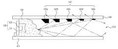
도 2a는 도 1의 백라이트 유닛의 단면도이고, 도 2b는 도 2a의 A부분의 확대도이다.FIG. 2A is a cross-sectional view of the backlight unit of FIG. 1, and FIG. 2B is an enlarged view of a portion A of FIG. 2A.
실시예에 따른 백라이트 유닛(110)은, 발광소자 패키지 어레이(125)가 고정된 회로기판(121)을 포함하는 광원 유닛(120)과 상기 발광소자 패키지에서 방출되는 빛을 전달하는 렌즈(130)를 포함하는 광원 모듈과, 상기 광원 모듈에서 전달된 빛을 확산시트(140)로 전달하는 반사시트(111)와, 상기 렌즈(130)와 반사시트(111)로부터 전달된 빛을 패널 방향으로 투사하는 확산시트(140)를 포함하여 이루어진다.The
여기서, 상기 확산시트(140)는 프리즘 시트, 마이크로 렌즈 어레이 등을 포함하는 광학시트의 일실시예임은 상술한 바와 동일하다.Here, the
상기 광원 유닛(120)은 광원(125)과 상기 광원(125)이 배열되는 회로기판(121)을 포함할 수 있다. 그리고, 상기 광원(125)은 상기 렌즈(130) 방향으로 빛을 방출할 수 있게 구비된다. 여기서, 상기 광원(125)은 광원이 복수 개 배치된 광원 어레이의 형태로 구비될 수 있으며, 발광 다이오드 패키지(Light emitting diode package)일 수 있다.The
그리고, 상기 렌즈(130)는 상기 광원 유닛(120)에서 방출되는 빛을 산란시켜 그 빛이 반사시트(111)와 확산시트(140)의 전체 영역에 걸쳐 분포되도록 한다. 따라서, 광투과율이 좋은 재료로 이루어지는데, 일 예로써 폴리메틸메타크릴레이트(PolyMethylMethAcrylate; PMMA), 폴리카보네이트(PolyCarbonate; PC), 폴리에틸렌(PolyEthylene; PE) 또는 레진 사출물로 이루어질 수 있다.The
그리고, 상기 렌즈(130)는 도시된 바와 같이 광원 유닛(120)으로부터 방출된 빛의 입사각이 임계각 이상인 제1 면(136)과 임계각 미만인 제2 면(138)이 각각 적어도 1개씩 구비될 수 있다. 그리고, 도시된 바와 같이 상기 렌즈(130)에는 상기 제1 면(136)과 제2 면(138)이 적어도 2회 반복하여 배치될 수 있다.As shown in the drawing, the
상술한 렌즈(130)의 구성으로 인하여 광원 유닛(120)으로부터 입사된 빛이 일부는 투과되고 일부는 렌즈(130) 내부로 전반사된 후 다시 투사되므로, 반사시트(111)과 확산시트(140) 방향으로 투사되는 빛이 고르고 더 멀리 분포할 수 있다.The
상세히 설명하면 아래와 같다.The details will be described below.
광학적으로 밀한 매질에서 소한 매질로 빛이 진행할 때, 임계각보다 큰 입사각으로 입사한 빛은 굴절하지 않고 내부로 100% 반사되는 현상을 전반사라고 한다. 전반사가 일어날 수 있는 입사각의 최소값을 임계각이라 한다.When light travels from an optically dense medium to a small medium, the incident light that is incident at an incident angle larger than the critical angle is not refracted but is 100% reflected internally. The minimum value of incident angle at which total internal reflection can occur is called critical angle.
실시예에서 전반사가 일어나기 위하여 상기 렌즈(130)는 공기보다 밀한 물질이어야 하며, 굴절률이 1 이상일 수 있다. 그리고, 광원 유닛(120)으로부터 방출된 빛 중 렌즈(130)의 제1 면(136)으로 입사된 빛이 렌즈의 법선과 이루는 각도(θ1)가 임계각(θc)보다 크므로 상기 빛은 렌즈(130) 내부로 전반사된다.In order to cause total reflection in the embodiment, the
그리고, 상기 광원 유닛(120)으로부터 방출된 빛 중 렌즈(130)의 제2 면(138)으로 입사된 빛이 렌즈의 법선과 이루는 각도(θ2)가 임계각(θc)보다 작으므로 상기 빛은 모두 렌즈(130) 외부로 굴절되며, 이때 굴절각도는 스넬의 법칙에 따른다.Since the angle θ2 formed by the light incident on the
본 실시예에서는 제1 면(136) 사이에 복수 개의 제2 면(138a, 138b, 138c)이 배치되어 있으며, 상기 제1 면(136)과 제2 면(138)로 입사되는 빛의 입사각은 각각 임계각(θc) 이상이거나 미만이므로, 빛이 일부는 외부로 굴절되고 일부는 내부로 전반사된다.In this embodiment, a plurality of
예를 들면 렌즈(130)를 유리로 만들면, 유리로 이루어진 렌즈(130)에서 공기로 빛이 진행한다면 임계각은 42°이고, 입사각이 이보다 크면 빛이 모두 렌즈(130) 내면으로 반사되어 공기 쪽으로는 나가지 않는다. 따라서, 상기 제1 면(136)과 제2 면(138)은 광원 유닛(120)으로부터 입사되는 빛의 입사각이 임계각 이상인 면과 미만이 되도록 이루어져서, 렌즈(130)의 성능을 조절할 수 있다. 즉, 렌즈(130)로 입사된 빛은 손실 없이 멀리까지 전달될 수 있다. For example, if the
그리고, 상기 반사시트(111)는 상기 광원 모듈에서 방출된 빛이 면광원 형태로 출사되도록 반사하여 광효율을 제고하는 역할을 한다. 여기서, 상기 반사시트(111)는 별도의 구성요소로 마련될 수도 있고, 바텀 커버의 전면에 반사도가 높은 물질로 코팅되는 형태로 마련될 수도 있다.The
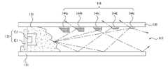
도 3a 내지 도 3c는 도 2a의 광원 모듈의 실시예들의 단면도이다.3A to 3C are cross-sectional views of embodiments of the light source module of FIG. 2A.
도 3a는 도 2a에 도시된 백라이트에 구비된 광원 모듈과 동일한 실시예가 도시되어 있으며, 도 3b에는 도 3a에 도시된 광원 모듈과 렌즈(130)가 상하 역전을 이루는 점에서 상이하다. 즉, 도 3a와 도 3b에 도시된 실시예에 따른 광원 모듈은 모두 빛의 전반사와 굴절을 통하여 백라이트 유닛(110)의 먼 위치까지 고르게 광을 전달할 수 있다.3A is the same as the light source module provided in the backlight shown in FIG. 2A, and FIG. 3B is different in that the light source module shown in FIG. 3A and the
그리고, 렌즈(130)는 광원 유닛(120)으로부터 빛이 입사되는 광입사부(135)과 광전달부(131) 및 빛을 외부로 방출하는 제1 면(136)과 제2 면(138)로 이루어진다. 또한, 상기 렌즈(130)의 지지부(132)는 상기 광원 유닛(120)을 지지할 수 있고, 고정부(134)는 상기 광원 유닛(120)에 고정되어 상기 렌즈(130)과 상기 광원 유닛(120)이 일체를 이루게 한다.The
이때, 상기 발광소자 패키지 어레이(125)가 고정된 회로기판(Printed Circuit, 121)이 상기 렌즈(130) 상에 구비된 홈(133)에 삽입되어 고정되고 있다.At this time, a printed
또한, 도 3c에 도시된 실시예에서는 상기 렌즈(130)에 구비된 홈(133)과 상기 회로기판(121)이 수직이 아니게 형성되어 있다. 이러한 구성은, 발광소자 패키지 어레이(125)로부터 방출되는 빛이 확산시트(140)에 평행하게 투사되지 않고 반사시트(111) 방향으로 기울어지게 투사되도록 하기 위함이다. 여기서, 회로기판(121)은 확산시트(140)와 직각이 아니므로 예각 또는 둔각을 이룰 수 있다.In the embodiment shown in FIG. 3C, the
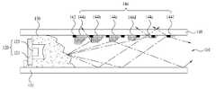
도 4a는 도 2a의 백라이트 유닛의 광분포를 나타낸 도면이고, 도 4b는 종래의 백라이트 유닛의 광분포를 나타낸 도면이다.FIG. 4A is a view showing the light distribution of the backlight unit of FIG. 2A, and FIG. 4B is a diagram showing the light distribution of the conventional backlight unit.
종래의 백라이트 유닛(110)에서는 LED 광원에서 방출된 빛은 램버시안(Lambertian) 산란 상태를 이루는데, 도 4b에 도시된 바와 같이 반사시트(111)와 확산시트(140)의 전면에 분포하지 못하고 광원 유닛(120)에서 가까운 부근에만 집중되며, 이러한 광분포의 불균일성은 표시장치의 휘도의 불균일로 이루어질 수 있다.In the
본 실시예에 따른 백라이트 유닛(110)은 상술한 구조의 렌즈(130) 내부에서 전반사를 거쳐 외부로 고르게 투사되므로, 반사시트(111)와 확산시트(140) 전체에 고르게 빛이 분포할 수 있다.Since the
실시예에 따른 백라이트 유닛(110)은 도광판을 사용하지 않으며, 렌즈(130)에서 전반사와 굴절에 따라 빛을 패널의 전면에 고르게 분포시킬 수 있다. 이때, 광원 모듈에 가까운 패널에 투사되는 빛의 양이 상대적으로 많을 수 있으므로, 빛을 패널의 전체에 고르게 투사하기 위하여 아래와 같은 구성을 가질 수 있다.The
도 5a 내지 도 5f는 백라이트 유닛의 다른 실시예들을 나타낸 도면이다. 실시예들에 따른 백라이트 유닛(110)은, 확산시트(140)의 내측면의 일부분에 광반사층(142) 또는 광산란층(144) 중 적어도 하나를 배치한다. 이때, 광원 모듈에 가까운 확산시트(140)에서 광반사층(142) 또는 광산란층(144)의 크기나 밀도를 조절할 수 있다.5A to 5F are views showing other embodiments of the backlight unit. The
도 5a에 도시된 실시예에서 확산시트(140)의 내측면에는 광반사층(142)가 배치되어 있다. 여기서, 내측면은 반사시트(111)를 향하는 방향을 뜻한다. 상기 광반사층(142)은 반사율이 높은 은(Ag)이나 알루미늄(Al) 등으로 이루어질 수 있다.In the embodiment shown in FIG. 5A, a
본 실시예에서는 광반사층(142)이 렌즈(130)에 가까운 곳에서 가장 폭이 넓으며, 각각의 광반사층(142) 간의 간격도 좁다. 즉, 렌즈(130)로부터 멀어질수록 광반사층(142a, 142b,142c, 142d, 142e, 142f, 142g)의 폭이 좁아지고 각각의 거리는 넓어지므로, 즉 밀도가 감소하므로 빛이 확산시트(140) 외부로 투과될 영역이 넓어진다.In this embodiment, the
따라서, 광량이 상대적으로 많은 렌즈(130)의 인접 영역에서 확산시트(140) 외부로 투과되는 빛의 양을 줄이므로, 전체적으로 확산시트(140) 외부로 투사되는 빛의 양을 고르게 조절할 수 있다. 이러한 구성은 광반사층(142)이 아닌 광산란층(144)의 분포를 도 5a에 같이 배치하여도 가능하다.Accordingly, since the amount of light transmitted to the outside of the
도 5b에 도시된 실시예는 광반사층(142)과 광산란층(144)이 함께 확산시트(14)의 내측면에 구비되어 있다. 이때, 광반사층(142)은 도 5a에 도시된 바와 같이 렌즈(130)로부터 멀어질수록 광반사층(142a, 142b,142c, 142d, 142e, 142f, 142g)의 폭이 좁아지고 각각의 거리는 넓어진다.In the embodiment shown in FIG. 5B, the
그리고, 광산란층(144)는 각각의 폭과 간격이 모두 동일하게 구비되어 있으며, 일부 광산란층(144)은 광반사층(142) 상에 구비되며 일부 광산란층(144)는 확산시트(140) 상에 직접 구비되어 있다. 상기 광산란층(144)은 TiO2 또는 Al2O3로 이루어질 수 있는데, 광학시트(140)의 전체 개구부를 차폐하지는 않고 있다.The
본 실시예에서는 도 5a와 같은 배치를 갖는 광반사층(142)과 동일한 배치 내지 밀도를 갖는 광산란층(144)이 구비되어, 확산시트(140) 외부로 투사되는 빛의 분포를 고르게 할 수 있다.In this embodiment, the
도 5c에 도시된 실시예에는 도 5b에 도시된 실시예와 달리 광반사층(142)이 일정한 폭과 간격으로 배치되고, 광산란층(144)이 렌즈(130)로부터 멀어질수록 밀도가 감소하게 배치된다.5c, the light reflection layers 142 are arranged at a constant width and spacing, and the
즉, 렌즈(130)로부터 멀어질수록 광반사층(144a, 144b, 144c, 144d, 144e, 144f의 폭이 좁아지고 각각의 거리는 넓어지므로, 즉 밀도가 감소하므로 빛이 확산시트(140) 외부로 투과될 영역이 넓어진다.That is, as the width of the
도 5d에 도시된 실시예에서는 광반사층(142)이 복수 개의 층(142a, 142b, 142c, 142d, 142e)으로 이루어지며, 렌즈(130)로부터 멀어질수록 상기 광반사층(142)의 밀도가 감소한다.In the embodiment shown in FIG. 5D, the
즉, 광원 유닛(120) 내지 광원 모듈로부터 멀어질수록, 광반사층(142)을 이루는 복수 개의 층(142a, 142b, 142c, 142d, 142e)이 각각 폭이 좁아지고 서로 간의 간격이 더 커지므로 확산시트(140)의 외부로 빛이 투과될 영역이 넓어진다.That is, since the plurality of
도 5e에 도시된 실시예에서는 광산란층(144)이 복수 개의 층(144a, 144b, 144c, 144d, 144e)으로 이루어지며, 렌즈(130)로부터 멀어질수록 상기 광산란층(144)의 밀도가 감소한다. In the embodiment shown in FIG. 5E, the
즉, 광원 유닛(120) 내지 광원 모듈로부터 멀어질수록, 광산란층(144)을 이루는 복수 개의 층(144a, 144b, 144c, 144d, 144e)이 각각 폭이 좁아지고 서로 간의 간격이 더 커지므로 확산시트(140)의 외부로 빛이 투과될 영역이 넓어진다.That is, since the plurality of
도 5d와 도 5e에 도시된 구성은 광반사층(142)과 광산란층(144)이 복수 개의 층으로 이루어지고, 광원 유닛(120)으로부터 가까운 거리에서 각각의 광반사층(142)과 광산란층(144)의 배열 뿐만 아니라 두께가 더 두껍게 구비되어 있다.5D and 5E show that the
즉, 확산시트(140) 전체에 광반사층(142) 또는 광산란층(144)을 형성한 후, 2회의 공정에서는 광원 유닛(120)에서 가장 먼 영역을 제외하고 광반사층(142) 또는 광산란층(144)을 형성할 수 있으며, 다음 공정에서는 상기 광원 유닛(120)에 보다 인접한 영역에만 광반사층(142) 또는 광산란층(144)을 형성할 수 있다. 따라서, 광반사층(142)과 광확산층(144)의 폭과 간격 및 두께를 통하여 밀도를 조절하고, 그에 따라 빛의 반사 정도를 조절할 수 있다.That is, after the
도 5f에 도시된 실시예에서는 광반사층(142)은 동일한 폭과 간격으로 구비되어 있으며, 광산란층(144)이 복수 개의 층(144a, 144b, 144c, 144d, 144e)으로 이루어지며, 렌즈(130)로부터 멀어질수록 상기 광산란층(144)의 밀도가 감소한다.5f, the
즉, 광산란층(144)의 매치는 도 5e에 도시된 실시예와 유사하나, 복수 개의 층으로 이루어진 광산란층(144a, 144b, 144c, 144d, 144e)에서 패턴이 일치하는 위치가 상이하다.That is, the matching of the light-
상술한 도 5a 내지 도 5f에 도시된 실시예들에서는, 광학시트(140)의 내측면에 광반사층(142)과 광산란층(144)을 배치하고, 상기 광반사층(142)과 광산란층(144)의 밀도(폭 및/또는 간격)를 조절하여 개구율이 렌즈(130)로부터 멀어질수록 증가하도록 배치하여, 광분포의 균일성을 증진시키고 있다.5A to 5F, the
도 6a 및 도 6b는 백라이트 유닛의 또 다른 실시예들을 나타낸 도면이다.6A and 6B are views showing still another embodiment of the backlight unit.
실시예들은 도 2a에 도시된 실시예와 유사하나, 도 6a에 도시된 실시예는 반사시트(111)가 기울어져 배치된다. 즉 종래에는 광학시트 내지 확산시트(140)과 반사시트(111)가 나란하나, 실시예에 따른 백라이트 유닛(110)은 반사시트(111)가 상기 광학시트 내지 확산시트(140)에 대하여 기울어진다.The embodiments are similar to the embodiment shown in Fig. 2A, but the embodiment shown in Fig. 6A is arranged such that the
이러한 반사시트(111)의 기울기는 특히 렌즈(130)와 먼 영역에서 빛의 반사를 용이하게 할 수 있다.The inclination of the
그리고, 도 6b에 도시된 실시예에서는 반사시트(111)가 직선으로 기울어지지 않고, 곡률을 가지고 휘어지며 기울어짐으로써 상술한 작용을 구현할 수 있다.In the embodiment shown in FIG. 6B, the
또한, 이상에서 실시예를 중심으로 설명하였으나 이는 단지 예시일 뿐 본 발명을 한정하는 것이 아니며, 본 발명이 속하는 분야의 통상의 지식을 가진 자라면 본 실시예의 본질적인 특성을 벗어나지 않는 범위에서 이상에 예시되지 않은 여러 가지의 변형과 응용이 가능함을 알 수 있을 것이다. 예를 들어, 실시예에 구체적으로 나타난 각 구성 요소는 변형하여 실시할 수 있는 것이다. 그리고 이러한 변형과 응용에 관계된 차이점들은 첨부된 청구 범위에서 규정하는 본 발명의 범위에 포함되는 것으로 해석되어야 할 것이다.While the present invention has been particularly shown and described with reference to exemplary embodiments thereof, it is clearly understood that the same is by way of illustration and example only and is not to be taken by way of illustration, It can be seen that various modifications and applications are possible. For example, each component specifically shown in the embodiments can be modified and implemented. It is to be understood that all changes and modifications that come within the meaning and range of equivalency of the claims are therefore intended to be embraced therein.
100 : 표시장치 110 : 백라이트 유닛
111 : 반사시트 120 : 광원 유닛
121 : 회로기판 125 : 발광소자 패키지 어레이
130 : 렌즈 131 : 광전달부
132 : 지지부 133 : 고정부
134 : 고정부 135 : 광입사부
136 : 제1 면 138 : 제2 면
140 : 확산시트 142 : 광반사층
144 : 광확산층 150, 160 : 제1, 제2 프리즘시트
170 : 패널 180 : 컬러필터100: display device 110: backlight unit
111: reflective sheet 120: light source unit
121: circuit board 125: light emitting device package array
130: lens 131:
132: support portion 133:
134: fixing part 135: light incidence part
136: first side 138: second side
140: diffusion sheet 142: light reflection layer
144:
170: Panel 180: Color filter
Claims (21)
Translated fromKorean상기 광원 모듈에서 전달된 광을 반사하는 반사시트; 및
상기 렌즈로부터 출사되거나 상기 반사시트에서 반사된 광을 전달받아 투사하는 광학시트를 포함하고,
상기 렌즈는,
상기 광원으로부터 방출된 광을 입사하는 광 입사부;
상기 입사된 광을 출사하는 광 출사면; 및
상기 광 입사부와 상기 광 출사면 사이에 배치되는 광 전달부를 포함하고,
상기 광 출사면은
상기 광 전달부로부터의 광을 전반사시키며, 상기 반사시트와 상기 광학시트 사이에서 서로 이격되어 배치된 복수의 제1 면; 및
상기 광 전달부로부터의 광을 굴절시켜 출사하고, 인접한 상기 복수의 제1 면 사이 마다 배치된 제2 면을 포함하고,
상기 제1 면과 상기 제2 면은 적어도 2회 반복하여 배치되고,
상기 광원과 상기 광 출사면 사이의 거리는 상기 광학시트로부터 상기 반사시트에 접근할수록 증가하고,
상기 광 전달부는 상기 광학시트와 평행한 상기 광원의 중심축을 기준으로 비대칭 형상을 갖는 표시 장치.A light source unit and a lens, wherein the light source unit includes a light source and a circuit board on which the light source is disposed, the lens comprising: a light source module for transmitting light emitted from the light source unit;
A reflective sheet for reflecting light transmitted from the light source module; And
And an optical sheet that transmits light projected from the lens or reflected by the reflection sheet,
The lens,
A light incident portion for emitting light emitted from the light source;
A light outgoing surface for emitting the incident light; And
And a light transmitting portion disposed between the light incidence portion and the light exit surface,
The light-
A plurality of first surfaces arranged to be spaced apart from each other between the reflective sheet and the optical sheet, for totally reflecting light from the light transmitting portion; And
And a second surface disposed between the plurality of first surfaces adjacent to each other to refract and emit light from the light transmitting portion,
Wherein the first surface and the second surface are arranged repeatedly at least twice,
Wherein a distance between the light source and the light output surface increases as the reflective sheet is approached from the optical sheet,
Wherein the light transmitting portion has an asymmetric shape with respect to a central axis of the light source parallel to the optical sheet.
상기 렌즈는 굴절률이 1 이상인 고분자 물질인 표시 장치.The method according to claim 1,
Wherein the lens is a high molecular material having a refractive index of 1 or more.
상기 회로기판은 상기 렌즈 상에 구비된 홈에 삽입되어 고정되고,
상기 홈은 상기 회로기판이 상기 광학시트에 대하여 예각 또는 둔각을 이루도록 형성된 표시 장치.The method according to claim 1,
Wherein the circuit board is inserted and fixed in a groove provided on the lens,
And the groove is formed so that the circuit board is formed at an acute angle or an obtuse angle with respect to the optical sheet.
상기 반사시트는 상기 광학시트에 대하여 기울어져 배치된 표시 장치.The method according to claim 1,
Wherein the reflective sheet is disposed obliquely with respect to the optical sheet.
상기 반사시트는 휘어지며 배치된 표시 장치.The method according to claim 6,
Wherein the reflective sheet is bent and disposed.
상기 광학시트의 일부분 상에 구비되고, 상기 광을 상기 반사시트로 반사하는 광반사층을 더 포함하고,
상기 광반사층은 상기 광원 모듈으로부터 멀어질수록 밀도가 감소하는 표시 장치.The method according to claim 1,
Further comprising a light reflecting layer which is provided on a part of the optical sheet and reflects the light to the reflection sheet,
Wherein the light reflection layer decreases in density as the distance from the light source module increases.
상기 광반사층은 서로 이격된 복수의 광반사층을 포함하고,
상기 복수의 광반사층은 상기 광원 모듈으로부터 멀어질수록 면적이 감소하고,
상기 복수의 광반사층이 서로 이격된 간격은 상기 광원 모듈로부터 멀어질수록 증가하는 표시 장치.9. The method of claim 8,
Wherein the light reflecting layer includes a plurality of light reflecting layers spaced from each other,
The plurality of light reflection layers are reduced in area as they are away from the light source module,
Wherein a spacing between the plurality of light reflection layers is increased as the distance from the light source module increases.
상기 광학시트의 일부분 상에 구비되고, 상기 광을 상기 반사시트로 산란시키는 광산란층을 더 포함하고,
상기 광산란층은 상기 광원 모듈으로부터 멀어질수록 밀도가 감소하고, TiO2 또는 Al2O3로 이루어진 표시 장치.9. The method of claim 8,
And a light scattering layer provided on a part of the optical sheet for scattering the light to the reflection sheet,
Wherein the light scattering layer is made of TiO2 or Al2 O3 , the density of which decreases with distance from the light source module.
상기 광산란층은 복수의 광산란층을 포함하고,
상기 복수의 광산란층은 상기 광원 모듈으로부터 멀어질수록 면적이 감소하고,
상기 복수의 광산란층이 서로 이격된 간격은 상기 광원 모듈로부터 멀어질수록 증가하는 표시 장치.13. The method of claim 12,
Wherein the light scattering layer comprises a plurality of light scattering layers,
Wherein the plurality of light scattering layers are reduced in area away from the light source module,
Wherein a distance between the plurality of light scattering layers is increased as the distance from the light source module increases.
13. The display device according to claim 12, wherein the density of the light scattering layer and the density of the light reflection layer are equal to each other.
Priority Applications (8)
| Application Number | Priority Date | Filing Date | Title |
|---|---|---|---|
| KR1020100118022AKR101850428B1 (en) | 2010-11-25 | 2010-11-25 | Light emitting module, display device including the same |
| TW100120223ATWI465808B (en) | 2010-11-25 | 2011-06-09 | Backlight unit and display apparatus using the same |
| US13/157,824US8556442B2 (en) | 2010-11-25 | 2011-06-10 | Backlight unit and display apparatus using the same |
| EP11169545.8AEP2458430B1 (en) | 2010-11-25 | 2011-06-10 | Backlight unit and display apparatus using the same |
| JP2011130088AJP5936824B2 (en) | 2010-11-25 | 2011-06-10 | Backlight unit and display device using the same |
| CN201110166795.XACN102478188B (en) | 2010-11-25 | 2011-06-14 | The display device of back light unit and use back light unit |
| US14/043,886US8985798B2 (en) | 2010-11-25 | 2013-10-02 | Backlight unit and display apparatus using the same |
| US14/043,891US9140426B2 (en) | 2010-11-25 | 2013-10-02 | Backlight unit and display apparatus using the same |
Applications Claiming Priority (1)
| Application Number | Priority Date | Filing Date | Title |
|---|---|---|---|
| KR1020100118022AKR101850428B1 (en) | 2010-11-25 | 2010-11-25 | Light emitting module, display device including the same |
Publications (2)
| Publication Number | Publication Date |
|---|---|
| KR20120056468A KR20120056468A (en) | 2012-06-04 |
| KR101850428B1true KR101850428B1 (en) | 2018-05-31 |
Family
ID=46608604
Family Applications (1)
| Application Number | Title | Priority Date | Filing Date |
|---|---|---|---|
| KR1020100118022AExpired - Fee RelatedKR101850428B1 (en) | 2010-11-25 | 2010-11-25 | Light emitting module, display device including the same |
Country Status (1)
| Country | Link |
|---|---|
| KR (1) | KR101850428B1 (en) |
Families Citing this family (1)
| Publication number | Priority date | Publication date | Assignee | Title |
|---|---|---|---|---|
| CN115032831B (en)* | 2022-04-29 | 2023-06-13 | 荣耀终端有限公司 | Display equipment |
Citations (5)
| Publication number | Priority date | Publication date | Assignee | Title |
|---|---|---|---|---|
| JP2004004936A (en)* | 1994-05-27 | 2004-01-08 | Canon Inc | Display device |
| JP2008300194A (en)* | 2007-05-31 | 2008-12-11 | Harison Toshiba Lighting Corp | Hollow surface lighting device |
| JP2010040236A (en)* | 2008-08-01 | 2010-02-18 | Epson Imaging Devices Corp | Lighting system, electro-optical device, and electronic device |
| JP2010073685A (en)* | 2008-09-18 | 2010-04-02 | Samsung Electronics Co Ltd | Back light assembly |
| JP2010212021A (en)* | 2009-03-09 | 2010-09-24 | Harison Toshiba Lighting Corp | Vehicular lighting system |
- 2010
- 2010-11-25KRKR1020100118022Apatent/KR101850428B1/ennot_activeExpired - Fee Related
Patent Citations (5)
| Publication number | Priority date | Publication date | Assignee | Title |
|---|---|---|---|---|
| JP2004004936A (en)* | 1994-05-27 | 2004-01-08 | Canon Inc | Display device |
| JP2008300194A (en)* | 2007-05-31 | 2008-12-11 | Harison Toshiba Lighting Corp | Hollow surface lighting device |
| JP2010040236A (en)* | 2008-08-01 | 2010-02-18 | Epson Imaging Devices Corp | Lighting system, electro-optical device, and electronic device |
| JP2010073685A (en)* | 2008-09-18 | 2010-04-02 | Samsung Electronics Co Ltd | Back light assembly |
| JP2010212021A (en)* | 2009-03-09 | 2010-09-24 | Harison Toshiba Lighting Corp | Vehicular lighting system |
Also Published As
| Publication number | Publication date |
|---|---|
| KR20120056468A (en) | 2012-06-04 |
Similar Documents
| Publication | Publication Date | Title |
|---|---|---|
| JP5936824B2 (en) | Backlight unit and display device using the same | |
| US7448787B2 (en) | Prism sheet and backlight unit employing the same | |
| US7220026B2 (en) | Optical film having a structured surface with offset prismatic structures | |
| KR100951723B1 (en) | Optical Sheet of Backlight Unit | |
| US7416309B2 (en) | Optical film having a surface with rounded structures | |
| US7320538B2 (en) | Optical film having a structured surface with concave pyramid-shaped structures | |
| KR101621013B1 (en) | Display device | |
| KR101883839B1 (en) | Light emitting device module and bcklight unit including the same | |
| US7914179B2 (en) | Optical plate with V-shaped protrusions on both sides and backlight module using the same | |
| US20060103777A1 (en) | Optical film having a structured surface with rectangular based prisms | |
| CN101344609B (en) | Back light module and optical plate | |
| US20080037281A1 (en) | Optical plate and backlight module using the same | |
| US20070024994A1 (en) | Structured optical film with interspersed pyramidal structures | |
| KR20100028039A (en) | Semi-specular components in hollow cavity light recycling backlights | |
| JP2010108919A (en) | Planar light source device, and display using the same | |
| KR20080048759A (en) | Light guide unit, backlight unit and display device employing the same | |
| JP2009170205A (en) | Light guide plate, light guide plate connector, backlight unit, and display device | |
| US20090303414A1 (en) | Optical member with a scatter layer, and backlight assembly and display device having the same | |
| US8118469B2 (en) | Surface illuminating device and image display apparatus | |
| JP5533310B2 (en) | Light guide plate, surface light source device and display device | |
| US20110032449A1 (en) | Perforated backlight | |
| KR101804407B1 (en) | Backlight unit | |
| KR20010046581A (en) | Backlight device for display | |
| KR101850428B1 (en) | Light emitting module, display device including the same | |
| KR101735673B1 (en) | Backlight unit |
Legal Events
| Date | Code | Title | Description |
|---|---|---|---|
| PA0109 | Patent application | St.27 status event code:A-0-1-A10-A12-nap-PA0109 | |
| PG1501 | Laying open of application | St.27 status event code:A-1-1-Q10-Q12-nap-PG1501 | |
| PN2301 | Change of applicant | St.27 status event code:A-3-3-R10-R13-asn-PN2301 St.27 status event code:A-3-3-R10-R11-asn-PN2301 | |
| R17-X000 | Change to representative recorded | St.27 status event code:A-3-3-R10-R17-oth-X000 | |
| A201 | Request for examination | ||
| P11-X000 | Amendment of application requested | St.27 status event code:A-2-2-P10-P11-nap-X000 | |
| P13-X000 | Application amended | St.27 status event code:A-2-2-P10-P13-nap-X000 | |
| PA0201 | Request for examination | St.27 status event code:A-1-2-D10-D11-exm-PA0201 | |
| P22-X000 | Classification modified | St.27 status event code:A-2-2-P10-P22-nap-X000 | |
| P22-X000 | Classification modified | St.27 status event code:A-2-2-P10-P22-nap-X000 | |
| R18-X000 | Changes to party contact information recorded | St.27 status event code:A-3-3-R10-R18-oth-X000 | |
| E902 | Notification of reason for refusal | ||
| PE0902 | Notice of grounds for rejection | St.27 status event code:A-1-2-D10-D21-exm-PE0902 | |
| E13-X000 | Pre-grant limitation requested | St.27 status event code:A-2-3-E10-E13-lim-X000 | |
| P11-X000 | Amendment of application requested | St.27 status event code:A-2-2-P10-P11-nap-X000 | |
| P13-X000 | Application amended | St.27 status event code:A-2-2-P10-P13-nap-X000 | |
| E701 | Decision to grant or registration of patent right | ||
| PE0701 | Decision of registration | St.27 status event code:A-1-2-D10-D22-exm-PE0701 | |
| PR0701 | Registration of establishment | St.27 status event code:A-2-4-F10-F11-exm-PR0701 | |
| PR1002 | Payment of registration fee | St.27 status event code:A-2-2-U10-U11-oth-PR1002 Fee payment year number:1 | |
| PG1601 | Publication of registration | St.27 status event code:A-4-4-Q10-Q13-nap-PG1601 | |
| R18-X000 | Changes to party contact information recorded | St.27 status event code:A-5-5-R10-R18-oth-X000 | |
| R18-X000 | Changes to party contact information recorded | St.27 status event code:A-5-5-R10-R18-oth-X000 | |
| PR1001 | Payment of annual fee | St.27 status event code:A-4-4-U10-U11-oth-PR1001 Fee payment year number:4 | |
| PN2301 | Change of applicant | St.27 status event code:A-5-5-R10-R13-asn-PN2301 St.27 status event code:A-5-5-R10-R11-asn-PN2301 | |
| PN2301 | Change of applicant | St.27 status event code:A-5-5-R10-R11-asn-PN2301 | |
| PN2301 | Change of applicant | St.27 status event code:A-5-5-R10-R14-asn-PN2301 | |
| PR1001 | Payment of annual fee | St.27 status event code:A-4-4-U10-U11-oth-PR1001 Fee payment year number:5 | |
| PC1903 | Unpaid annual fee | St.27 status event code:A-4-4-U10-U13-oth-PC1903 Not in force date:20230414 Payment event data comment text:Termination Category : DEFAULT_OF_REGISTRATION_FEE | |
| PC1903 | Unpaid annual fee | St.27 status event code:N-4-6-H10-H13-oth-PC1903 Ip right cessation event data comment text:Termination Category : DEFAULT_OF_REGISTRATION_FEE Not in force date:20230414 |