KR101847355B1 - Thin-film transistor, method of manufacturing the same, and display device - Google Patents
Thin-film transistor, method of manufacturing the same, and display deviceDownload PDFInfo
- Publication number
- KR101847355B1 KR101847355B1KR1020170126056AKR20170126056AKR101847355B1KR 101847355 B1KR101847355 B1KR 101847355B1KR 1020170126056 AKR1020170126056 AKR 1020170126056AKR 20170126056 AKR20170126056 AKR 20170126056AKR 101847355 B1KR101847355 B1KR 101847355B1
- Authority
- KR
- South Korea
- Prior art keywords
- film
- resistance
- region
- thin film
- low
- Prior art date
- Legal status (The legal status is an assumption and is not a legal conclusion. Google has not performed a legal analysis and makes no representation as to the accuracy of the status listed.)
- Active
Links
Images


Classifications
- H—ELECTRICITY
- H10—SEMICONDUCTOR DEVICES; ELECTRIC SOLID-STATE DEVICES NOT OTHERWISE PROVIDED FOR
- H10D—INORGANIC ELECTRIC SEMICONDUCTOR DEVICES
- H10D30/00—Field-effect transistors [FET]
- H10D30/60—Insulated-gate field-effect transistors [IGFET]
- H10D30/67—Thin-film transistors [TFT]
- H10D30/674—Thin-film transistors [TFT] characterised by the active materials
- H10D30/6755—Oxide semiconductors, e.g. zinc oxide, copper aluminium oxide or cadmium stannate
- H01L29/7869—
- H01L29/41733—
- H01L29/45—
- H01L29/66742—
- H01L29/78618—
- H01L29/78696—
- H—ELECTRICITY
- H10—SEMICONDUCTOR DEVICES; ELECTRIC SOLID-STATE DEVICES NOT OTHERWISE PROVIDED FOR
- H10D—INORGANIC ELECTRIC SEMICONDUCTOR DEVICES
- H10D30/00—Field-effect transistors [FET]
- H10D30/01—Manufacture or treatment
- H10D30/021—Manufacture or treatment of FETs having insulated gates [IGFET]
- H10D30/031—Manufacture or treatment of FETs having insulated gates [IGFET] of thin-film transistors [TFT]
- H—ELECTRICITY
- H10—SEMICONDUCTOR DEVICES; ELECTRIC SOLID-STATE DEVICES NOT OTHERWISE PROVIDED FOR
- H10D—INORGANIC ELECTRIC SEMICONDUCTOR DEVICES
- H10D30/00—Field-effect transistors [FET]
- H10D30/60—Insulated-gate field-effect transistors [IGFET]
- H10D30/67—Thin-film transistors [TFT]
- H10D30/6704—Thin-film transistors [TFT] having supplementary regions or layers in the thin films or in the insulated bulk substrates for controlling properties of the device
- H10D30/6713—Thin-film transistors [TFT] having supplementary regions or layers in the thin films or in the insulated bulk substrates for controlling properties of the device characterised by the properties of the source or drain regions, e.g. compositions or sectional shapes
- H—ELECTRICITY
- H10—SEMICONDUCTOR DEVICES; ELECTRIC SOLID-STATE DEVICES NOT OTHERWISE PROVIDED FOR
- H10D—INORGANIC ELECTRIC SEMICONDUCTOR DEVICES
- H10D30/00—Field-effect transistors [FET]
- H10D30/60—Insulated-gate field-effect transistors [IGFET]
- H10D30/67—Thin-film transistors [TFT]
- H10D30/6729—Thin-film transistors [TFT] characterised by the electrodes
- H—ELECTRICITY
- H10—SEMICONDUCTOR DEVICES; ELECTRIC SOLID-STATE DEVICES NOT OTHERWISE PROVIDED FOR
- H10D—INORGANIC ELECTRIC SEMICONDUCTOR DEVICES
- H10D30/00—Field-effect transistors [FET]
- H10D30/60—Insulated-gate field-effect transistors [IGFET]
- H10D30/67—Thin-film transistors [TFT]
- H10D30/6757—Thin-film transistors [TFT] characterised by the structure of the channel, e.g. transverse or longitudinal shape or doping profile
- H—ELECTRICITY
- H10—SEMICONDUCTOR DEVICES; ELECTRIC SOLID-STATE DEVICES NOT OTHERWISE PROVIDED FOR
- H10D—INORGANIC ELECTRIC SEMICONDUCTOR DEVICES
- H10D64/00—Electrodes of devices having potential barriers
- H10D64/60—Electrodes characterised by their materials
- H10D64/62—Electrodes ohmically coupled to a semiconductor
- H—ELECTRICITY
- H10—SEMICONDUCTOR DEVICES; ELECTRIC SOLID-STATE DEVICES NOT OTHERWISE PROVIDED FOR
- H10D—INORGANIC ELECTRIC SEMICONDUCTOR DEVICES
- H10D99/00—Subject matter not provided for in other groups of this subclass
Landscapes
- Thin Film Transistor (AREA)
- Liquid Crystal (AREA)
- Devices For Indicating Variable Information By Combining Individual Elements (AREA)
Abstract
Translated fromKoreanDescription
Translated fromKorean[관련 출원의 상호 참조][Cross reference of related application]
본 출원은 각각 2010년 3월 30일 및 2010년 11월 1일에 일본 특허청에 출원된 일본 특허 출원 제2010-079293호 및 제2010-245035호를 우선권 주장하며, 참조로 이의 전체 내용이 본 명세서에 원용된다.This application claims priority to Japanese Patent Application Nos. 2010-079293 and 2010-245035 filed with the Japanese Patent Office on March 30, 2010 and November 1, 2010, the entire contents of which are incorporated herein by reference .
본 발명은 산화물 반도체를 사용한 박막 트랜지스터(thin-film transistor)와, 그 제조 방법 및 박막 트랜지스터를 구비한 디스플레이 장치에 관한 것이다.The present invention relates to a thin-film transistor using an oxide semiconductor, a method of manufacturing the same, and a display device including the thin-film transistor.
액티브 구동 방식의 액정 디스플레이 장치 및 액티브 구동 방식의 유기 전계 발광(이하, 간단히 "EL(electroluminescence)" 이라 함) 디스플레이 장치에서는, 각각 박막 트랜지스터(TFT; Thin-film transistor)를 구동 소자로서 사용하며, 영상을 기입하기 위한 신호 전압에 대응하는 전하를 유지 용량에 유지시킨다. 그러나, 박막 트랜지스터의 게이트 전극과 소스 전극, 또는 박막 트랜지스터의 게이트 전극과 드레인 전극의 교차 영역에 발생하는 기생 용량이 커지면, 신호 전압이 변동하게 되어, 화질의 열화를 초래할 우려가 있다.A thin film transistor (TFT) is used as a driving element in each of an active driving type liquid crystal display device and an active driving type organic electroluminescence (hereinafter simply referred to as "EL (electroluminescence) The charge corresponding to the signal voltage for writing the image is held in the holding capacitor. However, if the parasitic capacitance generated between the gate electrode and the source electrode of the thin film transistor, or between the gate electrode and the drain electrode of the thin film transistor becomes large, the signal voltage fluctuates and the image quality may deteriorate.
특히, 유기 EL 디스플레이 장치에서, 기생 용량이 큰 경우에는 유지 용량도 크게 할 필요가 있고, 화소의 레이아웃을 배선 등이 차지하는 비율이 커진다. 그 결과, 배선간의 쇼트 등의 확률이 증가하고, 제조 수율이 저하된다는 문제가 발생한다.Particularly, in the organic EL display device, when the parasitic capacitance is large, it is necessary to increase the storage capacitance, and the ratio of the layout of the pixels occupied by the wiring or the like becomes large. As a result, there arises a problem that the probability of a short circuit or the like between the wirings increases and the manufacturing yield decreases.
이러한 문제점을 해결하기 위해서, 예를 들어 산화 아연(ZnO) 또는 산화 인듐 갈륨 아연(IGZO) 등의 산화물 반도체를 채널에 사용한 박막 트랜지스터에 있어서, 게이트 전극과 소스 전극 또는 드레인 전극과의 교차 영역에 형성되는 기생 용량을 저감하려는 시도가 이루어지고 있다.In order to solve this problem, in a thin film transistor using, for example, an oxide semiconductor such as zinc oxide (ZnO) or indium gallium gallium oxide (IGZO) as a channel, a gate electrode is formed in a crossing region with a source electrode or a drain electrode An attempt has been made to reduce the parasitic capacitance.
예를 들어 일본 미심사 특허 출원 공보 제2007-220817(JP2007-220817A)호와, J.Park 등의 "Self-aligned top-gate amorphous gallium indium zinc oxide thin film transistors", Applied Physics Letters,American Institute of Physics,2008년, 제93권,053501 (비특허 문헌 1)에는 각각 셀프 얼라인 탑 게이트(self-aligned top-gate) 박막 트랜지스터가 개시되어 있다. 각각의 상기 개시된 박막 트랜지스터들에서는, 산화물 반도체 박막층의 채널 영역 상에 게이트 전극 및 게이트 절연막을 동일 형상으로 형성한 후에, 게이트 전극 및 게이트 절연막에 의해 덮어져 있지 않은 산화물 반도체 박막층의 영역을 저-저항화하여 소스-드레인 영역을 형성한다. 또한, R. Hayashi 등의 "Improved Amorphous In-Ga-Zn-O TFTs", SID 08 DIGEST, 2008년 42. 1, 621-624 (비특허 문헌 2)에는, 게이트 전극을 마스크로 한 이면 노광에 의해 산화물 반도체막에 소스 영역 및 드레인 영역을 형성하는 셀프 얼라인 구조의 보텀(bottom)-게이트 박막 트랜지스터가 개시되어 있다.For example, Japanese Unexamined Patent Application Publication No. 2007-220817 (JP2007-220817A) and J. Park, "Self-aligned top-gate amorphous gallium indium zinc oxide thin film transistors ", Applied Physics Letters, Physics, 2008, Vol. 93, 053501 (Non-Patent Document 1) discloses a self-aligned top-gate thin film transistor. In each of the above-described thin film transistors, after the gate electrode and the gate insulating film are formed in the same shape on the channel region of the oxide semiconductor thin film layer, the region of the oxide semiconductor thin film layer not covered with the gate electrode and the gate insulating film is formed as a low- To form a source-drain region. In "Improved Amorphous In-Ga-Zn-O TFTs" by R. Hayashi et al.,
JP2007-220817A 및 비특허 문헌 2에는, 저-저항의 소스-드레인 영역이 셀프 얼라인 방식으로 형성되도록, 층간 절연막으로서 플라즈마 CVD(chemical vapor deposition) 법에 의해 실리콘 질화막을 형성하고, 이 실리콘 질화막에 포함되는 수소를 산화물 반도체 박막층에 도입하는 것이 개시되어 있다. 또한, JP2007-220817A에는, 실리콘 질화막으로부터의 수소 도입에 부가하여, 수소 가스를 이용하는 플라즈마 처리를 병용하는 것이 개시되어 있다. 또한, 비특허 문헌 1에는, 아르곤 가스를 이용하는 플라즈마 분위기에 산화물 반도체막을 노출하여 저-저항의 소스-드레인 영역을 형성하는 것이 개시되어 있다. JP2007-220817A 및 비특허 문헌 1 및 2에 개시된 이들 내용을 포함하는 기존의 교시는, 소자 특성이 변동 요인이 많은 플라즈마 공정에 의존하므로, 이들 교시를 안정적으로 양산에 적용하는 것이 어렵다는 문제가 있었다.In JP2007-220817A and Non-Patent
셀프 얼라인 구조를 가지는 박막 트랜지스터의 특성을 안정시킬 수 있는 박막 트랜지스터 및 그 제조 방법, 및 이러한 박막 트랜지스터를 구비한 디스플레이 장치를 제공하는 것이 바람직하다.It is desirable to provide a thin film transistor capable of stabilizing characteristics of a thin film transistor having a self-aligned structure, a method of manufacturing the same, and a display device having such a thin film transistor.
본 실시예에 따른 제1 박막 트랜지스터에서는, 소스 영역 및 드레인 영역 각각의 상면으로부터 깊이 방향으로 연장하는 소스 영역 및 드레인 영역 각각의 적어도 일부에, 알루미늄, 붕소, 갈륨, 인듐, 티타늄, 실리콘, 게르마늄, 주석 및 납으로 이루어지는 군 중 적어도 일종을 도펀트로서 포함하는 저-저항 영역이 제공된다. 따라서, 소자 특성이 안정화된다.In the first thin film transistor according to this embodiment, at least a portion of each of the source region and the drain region extending in the depth direction from the upper surface of each of the source region and the drain region may be formed of at least one of aluminum, boron, gallium, indium, titanium, A low-resistance region containing at least one of the group consisting of tin and lead as a dopant is provided. Therefore, the device characteristics are stabilized.
본 실시예에 따른 박막 트랜지스터는 소스 영역 및 드레인 영역 각각의 상면으로부터 깊이 방향으로 연장하는 소스 영역 및 드레인 영역 각각의 적어도 일부에, 채널 영역보다도 산소 농도가 낮은 저-저항 영역이 제공된다. 따라서, 소자 특성이 안정화된다.In the thin film transistor according to the present embodiment, at least a part of each of the source region and the drain region extending in the depth direction from the upper surface of each of the source region and the drain region is provided with a low-resistance region having a lower oxygen concentration than the channel region. Therefore, the device characteristics are stabilized.
본 발명의 일 실시예에서는 박막 트랜지스터가 제공된다. 박막 트랜지스터는 소스 영역, 드레인 영역 및 채널 영역을 포함하는 산화물 반도체층을 포함하며, 소스 및 드레인 영역들의 일부는 채널 영역보다 낮은 산소 농도를 갖는다.In one embodiment of the present invention, a thin film transistor is provided. The thin film transistor includes an oxide semiconductor layer including a source region, a drain region, and a channel region, and a part of the source and drain regions have an oxygen concentration lower than the channel region.
본 발명의 일 실시예에 있어서, 소스 및 드레인 영역들의 일부는 소스 및 드레인 영역들의 상면으로부터 깊이 방향으로 연장하는 저-저항 영역이다.In one embodiment of the present invention, a portion of the source and drain regions is a low-resistance region extending in the depth direction from the top surface of the source and drain regions.
본 발명의 일 실시예에 있어서, 저-저항 영역은 소스 및 드레인 영역들의 상면으로부터 깊이 방향으로 10nm 이내로 연장된다.In one embodiment of the present invention, the low-resistance region extends within 10 nm in the depth direction from the top surface of the source and drain regions.
본 발명의 일 실시예에 있어서, 고-저항 재료층은 소스 및 드레인 영역들의 적어도 일부에 형성된다.In one embodiment of the present invention, a high-resistance material layer is formed on at least a portion of the source and drain regions.
본 발명의 일 실시예에 있어서, 고-저항 재료층은 산화 티타늄, 산화 알루미늄 및 산화 인듐으로 이루어진 군으로부터 선택된다.In one embodiment of the present invention, the high-resistance material layer is selected from the group consisting of titanium oxide, aluminum oxide and indium oxide.
본 발명의 일 실시예에 있어서, 고-저항 재료층은 복수의 섬 형상의 금속막을 포함한다.In one embodiment of the present invention, the high-resistance material layer comprises a plurality of island-shaped metal films.
본 발명의 일 실시예에 있어서, 섬 형상의 금속막은 간극이 제공되도록 이격되어 있다.In one embodiment of the present invention, the island-like metal film is spaced apart to provide a gap.
본 발명의 일 실시예에 있어서, 소스 및 드레인 영역들의 일부는 소스 및 드레인 영역들의 상면으로부터 깊이 방향으로 연장하는 저-저항 영역이며, 상기 섬 형상의 금속막의 제1 부분은 저-저항 영역과 접촉하고, 섬 형상의 금속막의 제2 부분은 게이트 전극과 접촉한다.In one embodiment of the present invention, a portion of the source and drain regions is a low-resistance region extending in the depth direction from the top surface of the source and drain regions, and a first portion of the island- And the second portion of the island-like metal film is in contact with the gate electrode.
본 발명의 일 실시예에 있어서, 박막 트랜지스터는 절연층을 더 포함한다.In one embodiment of the present invention, the thin film transistor further comprises an insulating layer.
본 발명의 일 실시예에 있어서, 박막 트랜지스터는 소스 전극 및 드레인 전극을 더 포함한다.In one embodiment of the present invention, the thin film transistor further includes a source electrode and a drain electrode.
본 발명의 일 실시예에 있어서, 박막 트랜지스터는 탑(top) 게이트 구조와 보텀(bottom) 게이트 구조 중 어느 하나로 구성된다.In one embodiment of the present invention, the thin film transistor is composed of either a top gate structure or a bottom gate structure.
본 발명의 일 실시예에서는 박막 트랜지스터가 제공된다. 박막 트랜지스터는 소스 영역, 드레인 영역 및 채널 영역을 포함하는 산화물 반도체층을 포함하며, 소스 영역 및 드레인 영역들의 일부는 알루미늄, 붕소, 갈륨, 인듐, 티타늄, 실리콘, 게르마늄, 주석, 납 및 이들의 혼합물로 이루어진 군으로부터 선택된 도펀트를 포함한다.In one embodiment of the present invention, a thin film transistor is provided. The thin film transistor includes an oxide semiconductor layer including a source region, a drain region and a channel region, and a portion of the source region and the drain regions are formed of a material selected from the group consisting of aluminum, boron, gallium, indium, titanium, silicon, germanium, tin, lead, ≪ / RTI >
본 발명의 일 실시예에 있어서, 소스 및 드레인 영역들의 일부는 소스 및 드레인 영역들의 상면으로부터 깊이 방향으로 연장하는 저-저항 영역이다.In one embodiment of the present invention, a portion of the source and drain regions is a low-resistance region extending in the depth direction from the top surface of the source and drain regions.
본 발명의 일 실시예에 있어서, 저-저항 영역은 소스 및 드레인 영역들의 상면으로부터 깊이 방향으로 적어도 30nm 이내로 연장한다.In one embodiment of the present invention, the low-resistance region extends in the depth direction from the top surface of the source and drain regions to at least 30 nm.
본 발명의 일 실시예에 있어서, 박막 트랜지스터는 소스 및 드레인 영역들의 적어도 일부에 형성되는 고-저항 재료층을 더 포함한다.In one embodiment of the present invention, the thin film transistor further comprises a high-resistance material layer formed in at least a portion of the source and drain regions.
본 발명의 일 실시예에 있어서, 고-저항 재료층은 티타늄, 알루미늄 및 인듐으로 이루어진 군으로부터 선택된 성분과, 붕소와, 갈륨과, 실리콘과, 게르마늄과, 주석과, 납을 포함한다.In one embodiment of the present invention, the high-resistance material layer comprises a component selected from the group consisting of titanium, aluminum and indium, boron, gallium, silicon, germanium, tin and lead.
본 발명의 일 실시예에 있어서, 고-저항 재료층은 복수의 섬 형상의 금속막과 복수의 섬 형상의 비금속막 중 어느 하나를 포함한다.In one embodiment of the present invention, the high-resistance material layer includes one of a plurality of island-shaped metal films and a plurality of island-shaped non-metal films.
본 발명의 일 실시예에 있어서, 섬 형상의 금속막과 섬 형상의 비금속막 중 어느 하나는 간극을 제공하도록 이격되어 있다.In one embodiment of the present invention, one of the island-shaped metal film and the island-shaped non-metal film is spaced apart to provide a gap.
본 발명의 일 실시예에 있어서, 소스 및 드레인 영역들의 일부는 소스 및 드레인 영역들의 상면으로부터 깊이 방향으로 연장하는 저-저항 영역이며, 섬 형상의 금속막과 섬 형상의 비금속막 중 어느 하나의 제1 부분은 저-저항 영역과 접촉하고, 섬 형상의 금속막과 섬 형상의 비금속막의 어느 하나의 제2 부분은 게이트 전극과 접촉한다.In one embodiment of the present invention, a part of the source and drain regions is a low-resistance region extending in the depth direction from the upper surface of the source and drain regions, The first portion is in contact with the low-resistance region, and the second portion of the island-shaped metal film and the island-shaped non-metal film is in contact with the gate electrode.
본 발명의 일 실시예에 있어서, 박막 트랜지스터는 절연층을 더 포함한다.In one embodiment of the present invention, the thin film transistor further comprises an insulating layer.
본 발명의 일 실시예에 있어서, 박막 트랜지스터는 소스 전극 및 드레인 전극을 더 포함한다.In one embodiment of the present invention, the thin film transistor further includes a source electrode and a drain electrode.
본 발명의 일 실시예에 있어서, 박막 트랜지스터는 탑 게이트 구조와 보텀 게이트 구조 중 어느 하나로 구성된다.In one embodiment of the present invention, the thin film transistor is composed of either a top gate structure or a bottom gate structure.
본 발명의 일 실시예에서는, 박막 트랜지스터의 제조 방법이 제공된다. 이 방법은 소스 영역, 드레인 영역 및 채널 영역을 포함하는 산화물 반도체층을 형성하는 단계를 포함하며, 소스 및 드레인 영역들의 일부는 채널 영역보다 낮은 산소 농도를 포함한다.In one embodiment of the present invention, a method of manufacturing a thin film transistor is provided. The method includes forming an oxide semiconductor layer comprising a source region, a drain region and a channel region, wherein a portion of the source and drain regions comprises an oxygen concentration lower than the channel region.
본 발명의 일 실시예에 있어서, 소스 및 드레인 영역들의 일부는 저-저항 영역이다. In one embodiment of the invention, some of the source and drain regions are low-resistance regions.
발명의 일 실시예에 있어서, 상기 방법은 금속층을 형성하는 단계와, 금속층을 열처리함으로써 저-저항 영역을 형성하는 단계를 더 포함한다. In one embodiment of the invention, the method further comprises forming a metal layer and forming a low-resistance region by heat treating the metal layer.
본 발명의 일 실시예에 있어서, 금속층은 어닐링 온도로 열 처리된다.In one embodiment of the present invention, the metal layer is heat treated to an annealing temperature.
본 발명의 일 실시예에 있어서, 상기 방법은 열처리 후에 금속층을 제거하는 단계를 더 포함한다.In one embodiment of the present invention, the method further comprises removing the metal layer after the heat treatment.
본 발명의 일 실시예에 있어서, 금속층은 복수의 섬 형상의 금속막을 포함한다.In one embodiment of the present invention, the metal layer includes a plurality of island-shaped metal films.
본 발명의 일 실시예에 있어서, 금속층은 소스 및 드레인 영역들 상에 형성된다.In one embodiment of the present invention, a metal layer is formed on the source and drain regions.
본 발명의 일 실시예에 있어서, 상기 방법은 절연층을 형성하는 단계를 더 포함한다.In one embodiment of the present invention, the method further comprises forming an insulating layer.
본 발명의 일 실시예에 있어서, 상기 방법은 소스 전극 및 드레인 전극을 더 포함한다.In one embodiment of the present invention, the method further comprises a source electrode and a drain electrode.
본 발명의 일 실시예에 있어서, 박막 트랜지스터는 보텀 게이트 구조와 탑 게이트 구조 중 어느 하나로 구성된다.In one embodiment of the present invention, the thin film transistor is composed of either a bottom gate structure or a top gate structure.
본 발명의 또 다른 실시예에서는 박막 트랜지스터의 제조 방법이 제공된다. 이 방법은 소스 영역, 드레인 영역 및 채널 영역을 포함하는 산화물 반도체층을 형성하는 단계를 포함하며, 소스 및 드레인 영역들의 일부는 알루미늄, 붕소, 갈륨, 인듐, 티타늄, 실리콘, 게르마늄, 주석, 납 및 이들의 혼합물로 이루어진 군으로부터 선택된 도펀트를 포함한다.In another embodiment of the present invention, a method of manufacturing a thin film transistor is provided. The method includes forming an oxide semiconductor layer comprising a source region, a drain region and a channel region, wherein a portion of the source and drain regions comprises at least one of aluminum, boron, gallium, indium, titanium, silicon, germanium, A mixture thereof, and a mixture thereof.
본 발명의 일 실시예에 있어서, 소스 및 드레인 영역들의 일부는 저-저항 영역이다.In one embodiment of the invention, some of the source and drain regions are low-resistance regions.
본 발명의 일 실시예에 있어서, 상기 방법은 금속층 및 비금속층 중 어느 하나를 형성하는 단계와, 금속층과 비금속층 중 어느 하나를 열처리함으로써 저-저항 영역을 형성하는 단계를 더 포함한다.In one embodiment of the present invention, the method further comprises forming either a metal layer or a non-metal layer and forming a low-resistance region by heat treating either the metal layer or the non-metal layer.
본 발명의 일 실시예에 있어서, 상기 방법은 열처리 후에 금속층과 비금속층 중 어느 하나를 제거하는 단계를 더 포함한다.In one embodiment of the present invention, the method further comprises removing either the metallic layer or the non-metallic layer after the heat treatment.
본 발명의 일 실시예에 있어서, 금속층은 복수의 섬 형상의 금속막을 포함하며, 비금속층은 복수의 섬 형상의 비금속막을 포함한다.In one embodiment of the present invention, the metal layer includes a plurality of island-shaped metal films, and the non-metal layer includes a plurality of island-shaped non-metal films.
본 발명의 일 실시예에 있어서, 금속층과 비금속층의 어느 하나는 소스 및 드레인 영역들 상에 형성된다.In one embodiment of the present invention, one of the metal layer and the non-metal layer is formed on the source and drain regions.
본 발명의 일 실시예에 있어서, 상기 방법은 절연층을 형성하는 단계를 더 포함한다.In one embodiment of the present invention, the method further comprises forming an insulating layer.
본 발명의 일 실시예에 있어서, 상기 방법은 소스 전극 및 드레인 전극을 형성하는 단계를 더 포함한다.In one embodiment of the present invention, the method further comprises forming a source electrode and a drain electrode.
본 발명의 일 실시예에 있어서, 박막 트랜지스터는 보텀 게이트 구조와 탑 게이트 구조 중 어느 하나로 구성된다.In one embodiment of the present invention, the thin film transistor is composed of either a bottom gate structure or a top gate structure.
본 발명의 실시예들의 박막 트랜지스터들의 각각에 따르면, 소스 영역 및 드레인 영역 각각의 상면으로부터 깊이 방향으로 연장하는 소스 영역 및 드레인 영역 각각의 적어도 일부에, 알루미늄, 붕소, 갈륨, 인듐, 티타늄, 실리콘, 게르마늄, 주석 및 납으로 이루어지는 군 중 적어도 일종을 도펀트로서 포함하거나 채널 영역보다도 산소 농도가 낮은 저-저항 영역을 제공한다. 그래서, 셀프 얼라인 구조를 가지는 박막 트랜지스터의 특성을 안정시킬 수 있다. 따라서, 이 박막 트랜지스터를 사용해서 디스플레이 장치를 구성하면, 기생 용량이 감소된 셀프 얼라인 구조와 함께 안정된 특성을 갖는 박막 트랜지스터에 의해, 고품질의 디스플레이가 가능해진다.According to each of the thin film transistors of the embodiments of the present invention, at least a portion of each of the source region and the drain region extending in the depth direction from the upper surface of each of the source region and the drain region is formed of aluminum, boron, gallium, indium, titanium, Germanium, tin, and lead as a dopant, or a low-resistance region having a lower oxygen concentration than the channel region. Thus, the characteristics of the thin film transistor having the self-aligning structure can be stabilized. Therefore, when the display device is constituted by using the thin film transistor, a high quality display can be realized by the thin film transistor having stable characteristics together with the self-aligning structure with reduced parasitic capacitance.
본 발명의 실시예들의 박막 트랜지스터의 제조 방법들 각각에 따르면, 산화물 반도체막의 채널 영역 상에 게이트 절연막 및 게이트 전극이 이 순서대로 동일 형상으로 형성된다. 이후, 산화물 반도체막, 게이트 절연막 및 게이트 전극 상에, 도펀트 재료막으로서 역할하는 금속막 또는 비금속막을 형성한다. 이후, 열처리에 의해 도펀트 재료막으로서 역할하는 금속막 또는 비금속막을 산화시켜 고-저항막으로 하고, 소스 영역 및 드레인 영역 각각의 상면으로부터 깊이 방향으로 연장하는 소스 영역 및 드레인 영역 각각의 적어도 일부에, 알루미늄, 붕소, 갈륨, 인듐, 티타늄, 실리콘, 게르마늄, 주석 및 납으로 이루어지는 군 중 적어도 일종을 도펀트로서 포함하거나 채널 영역보다도 산소 농도가 낮은 저-저항 영역을 형성한다. 그래서, 플라즈마 등의 변동 요소가 많은 공정을 사용하지 않고, 저-저항 영역을 형성할 수 있다. 따라서, 종래 기술과는 다르게, 소자 특성의 플라즈마 공정으로의 의존을 해소하고, 안정된 소자 특성을 얻는 것이 가능해진다.According to each of the thin film transistor manufacturing methods of the embodiments of the present invention, the gate insulating film and the gate electrode are formed in the same shape in this order on the channel region of the oxide semiconductor film. Thereafter, a metal film or a non-metal film serving as a dopant material film is formed on the oxide semiconductor film, the gate insulating film, and the gate electrode. Thereafter, a metal film or a non-metal film serving as a dopant material film is oxidized to form a high-resistance film by heat treatment, and at least a part of each of the source region and the drain region extending in the depth direction from the upper surface of each of the source region and the drain region, At least one of the group consisting of aluminum, boron, gallium, indium, titanium, silicon, germanium, tin and lead is included as a dopant or a low-resistance region having a lower oxygen concentration than the channel region is formed. Thus, a low-resistance region can be formed without using a process involving many fluctuation factors such as plasma. Therefore, unlike the prior art, reliance on the plasma process of the device characteristics can be solved, and stable device characteristics can be obtained.
추가적인 특징 및 이점들은 본 명세서에서 설명되며, 이하의 상세한 설명 및 도면으로부터 명확해질 것이다.Additional features and advantages are described herein and will become apparent from the following detailed description and drawings.
도 1는 본 발명의 제1 실시예에 따른 박막 트랜지스터의 구조를 나타내는 단면도.
도 2a 내지 도 2c는 도 1에 나타낸 박막 트랜지스터의 제조 방법을 공정순으로 나타내는 단면도.
도 3a 내지 도 3c는 도 2a 내지 도 2c에 계속되는 공정을 나타내는 단면도.
도 4는 채널 영역 및 저-저항 영역의 에너지 분산형 X-선 분광법(energy-dispersive X-ray spectroscopy)의 분석 결과를 나타내는 도면.
도 5a 및 도 5b는 도 1에 나타낸 박막 트랜지스터의 특성을 종래의 박막 트랜지스터의 특성과 대비해서 나타내는 도면.
도 6은 본 발명의 제2 실시예에 따른 박막 트랜지스터의 저-저항 영역의 알루미늄 농도의 측정 결과를 나타내는 도면.
도 7은 제1 변형예에 따른 박막 트랜지스터의 구성을 나타내는 단면도.
도 8a 내지 도 8c는 도 7에 나타낸 박막 트랜지스터의 제조 방법을 공정순으로 나타내는 단면도.
도 9는 본 발명의 제2 실시예에 따른 박막 트랜지스터의 구성을 나타내는 단면도.
도 10a 내지 도 10d는 도 9에 나타낸 박막 트랜지스터의 제조 방법을 공정순으로 나타내는 단면도.
도 11a 내지 도 11c는 도 10a 내지 도 10d에 계속되는 공정을 나타내는 단면도.
도 12는 제2 변형예에 따른 박막 트랜지스터의 구조를 나타내는 단면도.
도 13a 내지 도 13c는 도 12에 나타낸 박막 트랜지스터의 제조 방법을 공정순으로 나타내는 단면도.
도 14는 본 발명의 제3 실시예에 따른 박막 트랜지스터의 구조를 나타내는 단면도.
도 15는 섬 형상의 고-저항막의 일례를 나타내는 단면도.
도 16은 섬 형상의 고-저항막의 다른 예를 나타내는 단면도.
도 17은 섬 형상의 고-저항막의 크기를 설명하기 위한 도면.
도 18a 내지 도 18c는 도 14에 나타낸 박막 트랜지스터의 제조 방법을 공정순으로 나타내는 단면도.
도 19a 내지 도 19d는 도 18a 내지 도 18c에 나타낸 공정을 상세히 설명하기 위한 단면도.
도 20은 손톤(Thornton's model)의 모델을 나타내는 도면.
도 21a 및 도 21b는 도 14에 나타낸 박막 트랜지스터의 특성을 종래의 박막 트랜지스터의 특성과 대비해서 나타내는 도면.
도 22a 및 도 22b는 각각 고-저항막의 두께를 상이하게 하였을 경우의 박막 트랜지스터의 특성을 나타내는 도면.
도 23a 및 도 23b는 제3 변형예에 따른 박막 트랜지스터의 제조 방법을 공정순으로 나타내는 단면도.
도 24a 및 도 24b는 도 23a 및 도 23b에 계속되는 공정을 나타내는 단면도.
도 25a 및 도 25b는 제4 변형예에 따른 박막 트랜지스터의 제조 방법을 공정순으로 나타내는 단면도.
도 26a 및 도 26b는 도 25a 및 도 25b에 계속되는 공정을 나타내는 단면도.
도 27은 본 발명의 제4 실시예에 따른 박막 트랜지스터의 구조를 나타내는 단면도.
도 28a 내지 도 28d는 도 27에 나타낸 박막 트랜지스터의 제조 방법을 공정순으로 나타내는 단면도.
도 29a 내지 도 29c는 도 28a 내지 도 28d에 계속되는 공정을 나타내는 단면도.
도 30은 제1 적용 예에 따른 디스플레이 장치의 회로 구성을 나타내는 도면.
도 31은 도 30에 나타낸 화소 구동 회로의 일례를 나타내는 등가 회로도.
도 32는 제2 적용예의 외관을 나타내는 사시도.
도 33a는 제3 적용예의 전방측으로부터 본 외관을 나타내는 사시도이며, 도 33b는 제3 적용예의 이면측으로부터 본 외관을 나타내는 사시도.
도 34는 제4 적용예의 외관을 나타내는 사시도.
도 35은 제5 적용예의 외관을 나타내는 사시도.
도 36a는 제6 적용예의 개방된 상태의 정면도이며, 도 36b는 그 측면도이며, 도 36c는 폐쇄된 상태의 정면도이며, 도 36d는 좌측면도이며, 도 36e는 우측면도이며, 도 36f는 상면도이며, 도 36g는 하면도.
도 37은 도 1에 나타낸 박막 트랜지스터의 변형예를 나타내는 단면도.1 is a sectional view showing a structure of a thin film transistor according to a first embodiment of the present invention;
FIGS. 2A to 2C are cross-sectional views showing the manufacturing method of the thin film transistor shown in FIG.
Figs. 3A to 3C are cross-sectional views showing the process subsequent to Figs. 2A to 2C. Fig.
FIG. 4 is a diagram showing the results of energy-dispersive X-ray spectroscopy analysis of a channel region and a low-resistance region; FIG.
FIGS. 5A and 5B are diagrams showing the characteristics of the thin film transistor shown in FIG. 1 in comparison with the characteristics of a conventional thin film transistor. FIG.
6 is a diagram showing a measurement result of aluminum concentration in a low-resistance region of a thin film transistor according to a second embodiment of the present invention.
7 is a sectional view showing a configuration of a thin film transistor according to a first modification;
8A to 8C are cross-sectional views showing the manufacturing method of the thin film transistor shown in Fig. 7 in the order of the process.
9 is a sectional view showing a configuration of a thin film transistor according to a second embodiment of the present invention.
FIGS. 10A to 10D are cross-sectional views showing the manufacturing method of the thin film transistor shown in FIG.
Figs. 11A to 11C are cross-sectional views showing the process subsequent to Figs. 10A to 10D. Fig.
12 is a sectional view showing a structure of a thin film transistor according to a second modification;
13A to 13C are cross-sectional views showing the manufacturing method of the thin film transistor shown in Fig. 12 in the order of process.
14 is a sectional view showing the structure of a thin film transistor according to a third embodiment of the present invention.
15 is a cross-sectional view showing an example of an island-shaped high-resistance film.
16 is a cross-sectional view showing another example of an island-shaped high-resistance film;
17 is a view for explaining the size of the island-shaped high-resistance film.
FIGS. 18A to 18C are cross-sectional views showing the manufacturing method of the thin film transistor shown in FIG.
19A to 19D are sectional views for explaining the process shown in Figs. 18A to 18C in detail.
20 is a diagram showing a model of Thornton's model;
21A and 21B are diagrams showing the characteristics of the thin film transistor shown in FIG. 14 in comparison with the characteristics of a conventional thin film transistor.
22A and 22B are diagrams showing the characteristics of the thin film transistor when the thickness of the high-resistance film is made different, respectively.
23A and 23B are cross-sectional views showing a method of manufacturing the thin film transistor according to the third modification in the order of the process.
24A and 24B are cross-sectional views showing the process subsequent to FIGS. 23A and 23B;
25A and 25B are cross-sectional views showing the manufacturing method of the thin film transistor according to the fourth modification in the order of the process.
Figs. 26A and 26B are cross-sectional views showing the steps subsequent to Figs. 25A and 25B. Fig.
27 is a sectional view showing the structure of a thin film transistor according to a fourth embodiment of the present invention.
28A to 28D are cross-sectional views showing the manufacturing method of the thin film transistor shown in Fig. 27 in the order of process.
29A to 29C are cross-sectional views showing the process subsequent to Figs. 28A to 28D. Fig.
30 is a circuit diagram showing a circuit configuration of a display device according to a first application example;
31 is an equivalent circuit diagram showing an example of the pixel driving circuit shown in Fig.
32 is a perspective view showing the appearance of the second application example;
Fig. 33A is a perspective view showing the appearance of the third application example from the front side, and Fig. 33B is a perspective view showing the appearance of the third application example from the back side.
34 is a perspective view showing the external appearance of the fourth application example;
35 is a perspective view showing an appearance of the fifth application example;
36A is a front view of the open state of the sixth application example, FIG. 36B is a side view thereof, FIG. 36C is a front view of the closed state, FIG. 36D is a left side view, FIG. 36E is a right side view, And Fig. 36G is a bottom view.
37 is a sectional view showing a modification of the thin film transistor shown in Fig.
본 발명의 실시예에 따른 첨부 도면들을 참조하여 본 출원을 상세하게 설명한다. 이하의 순서로 설명한다.The present application will be described in detail with reference to the accompanying drawings in accordance with an embodiment of the present invention. Will be described in the following order.
1. 제1 실시예(금속의 산화를 이용해서 저-저항 영역을 형성한 탑-게이트 박막 트랜지스터의 실시예)1. First embodiment (embodiment of top-gate thin film transistor in which low-resistance region is formed by oxidation of metal)
2. 제2 실시예(도펀트를 이용해서 저-저항 영역을 형성한 탑 게이트 박막 트랜지스터의 실시예)2. Second Embodiment (Top Gate Thin Film Transistor in which Low-resistance Region is formed Using a Dopant)
3. 제1 변형예(고-저항막을 제거한 탑 게이트 박막 트랜지스터의 변형예)3. First Modification (Modification of Top Gate Thin Film Transistor Removing High-Resistance Film)
4. 제3 실시예(고-저항막을 남긴 보텀 게이트 박막 트랜지스터의 실시예)4. Third Embodiment (Embodiment of the bottom gate thin film transistor in which the high-resistance film is left)
5. 제2 변형예(고-저항막을 제거한 보텀 게이트 박막 트랜지스터의 변형예)5. Second Modification (Modification of the bottom gate thin film transistor in which the high-resistance film is removed)
6. 제4 실시예(고-저항막을 섬 형상으로 형성한 탑 게이트 박막 트랜지스터의 실시예)6. Fourth Embodiment (Top Gate Thin Film Transistor in which High-Resistance Film is Shaped)
7. 제3 변형예(금속막을 섬 형상에 패터닝한 뒤에 산화시켜 고-저항막을 형성하는 제조 방법의 변형예)7. Modification 3 (a modification of the manufacturing method of forming a high-resistance film by oxidizing a metal film after patterning it into an island shape)
8. 제4 변형예(금속막을 산화시켜 고-저항막을 형성한 뒤에 섬 형상으로 패터닝하는 제조 방법의 변형예)8. Fourth Modification (Modification of Manufacturing Method for Patterning Island Pattern After High-Resistance Film is Formed by Oxidizing Metal Film)
9. 제5 실시예(고-저항막을 섬 형상으로 형성한 보텀 게이트 박막 트랜지스터의 실시예)9. Fifth embodiment (embodiment of bottom-gate thin film transistor in which high-resistance film is formed in island shape)
10. 적용예10. Application Examples
[제1 실시예][First Embodiment]
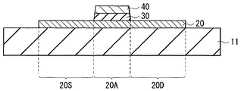
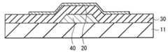
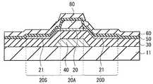
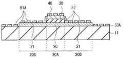
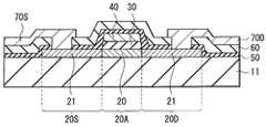
도 1은 본 발명의 제1 실시예에 따른 박막 트랜지스터(1)의 단면 구조를 나타낸다. 박막 트랜지스터(1)는 액정 디스플레이 및 유기 EL 디스플레이 등의 구동 소자로서 사용될 수 있는 것이다. 박막 트랜지스터(1)는, 예를 들어, 기판(11)에 산화물 반도체막(20), 게이트 절연막(30), 게이트 전극(40), 고-저항막(50), 층간 절연막(60), 소스 전극(70S) 및 드레인 전극(70D)이 이러한 순서대로 적층된 탑-게이트 구조(스태거(staggered) 구조)를 가질 수 있다.1 shows a sectional structure of a
기판(11)은, 예를 들어, 유리 기판, 플라스틱 필름 또는 다른 적절한 부재에 의해 구성되어도 좋다. 플라스틱 재료는, 예를 들어 PET(폴리에틸렌테레프탈레이트), PEN(폴리에틸렌나프탈레이트) 또는 다른 적절한 재료일 수 있다. 후술의 스퍼터링 공정에 있어서, 기판(11)을 가열함 없이 산화물 반도체막(20)을 성막하기 위해서 저렴한 플라스틱 필름을 사용할 수 있다. 기판(11)은 목적에 따라 스테인리스강(SUS) 등의 금속 기판이여도 좋다.The
산화물 반도체막(20)은, 기판(11) 상에 게이트 전극(40) 및 그 근방을 포함하는 섬 형상으로 설치되고, 박막 트랜지스터(1)의 활성층으로서의 기능을 갖는다. 산화물 반도체막(20)은, 두께가 50nm 정도일 수 있으며, 게이트 전극(40)에 대향하는 채널 영역(20A)을 가질 수 있다. 채널 영역(20A) 상에는, 게이트 절연막(30) 및 게이트 전극(40)이 이 순서대로 동일 형상으로 제공되어 있다. 채널 영역(20A)의 한쪽 측에는 소스 영역(20S)이 제공되며, 채널 영역(20A)의 다른 쪽의 측에는 드레인 영역(20D)이 제공되어 있다.The
채널 영역(20A)은 산화물 반도체에 의해 구성되어 있다. 본 명세서에 사용된 "산화물 반도체"란, 인듐, 갈륨, 아연, 주석 등의 일종 이상의 원소와, 산소를 포함하는 화합물을 가리킨다. 산화물 반도체는 비정질의 산화물 반도체 및 결정성의 산화물 반도체일 수 있다. 비정질의 산화물 반도체는 산화 인듐 갈륨 아연(IGZO)일 수 있다. 결정성의 산화물 반도체는 산화 아연(ZnO), 산화 인듐 아연(IZO; 등록 상표), 산화 인듐 갈륨(IGO), 산화 인듐 주석(ITO) 및 산화 인듐(InO) 일 수 있다.The
소스 영역(20S) 및 드레인 영역(20D)은, 각각, 상면으로부터 깊이 방향으로 연장하는 일부 영역에서 저-저항 영역(21)을 포함한다. 저-저항 영역(21)은, 예를 들어, 채널 영역(20A)보다 산소 농도가 낮은 것에 의해 저-저항화 되어 있다. 이에 의해, 이 박막 트랜지스터(1)는 셀프 얼라인 구조를 가지며, 특성을 안정화시킬 수 있다.The
저-저항 영역(21)의 산소 농도가 30%를 초과하면, 저항이 높아져 버리기 때문에, 저-저항 영역(21)의 산소 농도는 30% 이하인 것이 바람직하다.If the oxygen concentration in the low-
소스 영역(20S) 및 드레인 영역(20D) 각각의 저-저항 영역(21) 이외의 영역은, 채널 영역(20A)과 마찬가지로 산화물 반도체에 의해 구성되어 있다. 저-저항 영역(21)의 깊이에 대해서는 후술한다.The region other than the low-
게이트 절연막(30)은, 예를 들어, 두께가 300nm 정도이다. 게이트 절연막(30)은 실리콘 산화막, 실리콘 질화막, 실리콘 질화 산화막, 산화 알루미늄막 또는 다른 적절한 막의 단층막 또는 이들의 적층막에 의해 구성될 수 있다. 특히, 실리콘 산화막 또는 산화 알루미늄막은, 산화물 반도체막(20)을 환원시키기 어려우므로 바람직하다.The
게이트 전극(40)은, 박막 트랜지스터(1)에 게이트 전압을 인가하고, 이 게이트 전압으로 산화물 반도체막(20) 중의 전자 밀도를 제어하는 역할을 한다. 게이트 전극(40)은 기판(11) 상의 선택적인 영역에 제공된다. 예를 들어, 게이트 전극(40)은 두께가 10nm 내지 500nm, 구체적으로는 200nm 정도이며, 몰리브덴(Mo)으로 구성되어 있다. 게이트 전극(40)은 저-저항인 것이 바람직하므로, 게이트 전극(40)을 구성하는 재료로서는, 예를 들어, 알루미늄(Al), 구리(Cu) 또는 다른 적절한 금속 등의 저-저항 금속이 바람직하다. 저-저항층과 배리어층의 조합으로 이루어지는 적층막 또한 바람직하며, 이는 게이트 전극(40)의 저항을 낮추기 때문이다. 저-저항층은 알루미늄(Al), 구리(Cu) 또는 다른 적절한 성분으로 이루어질 수 있으며, 배리어층은 티타늄(Ti), 몰리브덴(Mo) 또는 다른 적절한 성분으로 이루어질 수 있다.The
고-저항막(50)은 층간 절연막(60)과 산화물 반도체막(20)과의 사이와, 층간 절연막(60)과 게이트 절연막(30)과의 사이와, 층간 절연막(60)과 게이트 전극(40)과의 사이에 제공되어 있다. 고-저항막(50)은, 후술하는 제조 공정에서 저-저항 영역(21) 내로 확산되는 금속의 공급원으로서 역할하는 금속막이 산화된 것이다. 고-저항막(50)은, 예를 들어, 산화 티타늄, 산화 알루미늄 또는 산화 인듐 또는 다른 적절한 산화물에 의해 구성될 수 있다. 산화 티타늄, 산화 알루미늄 또는 산화 인듐으로 이루어지는 고-저항막(50)은 외부 공기에 대하여 양호한 배리어성을 갖고, 산화물 반도체막(20)의 전기적 특성을 변화시키는 산소나 수분의 영향을 저감시킬 수 있다. 따라서, 고-저항막(50)을 제공함으로써, 박막 트랜지스터(1)의 전기 특성을 안정화시킬 수 있고, 층간 절연막(60)의 효과를 보다 높일 수 있다. 고-저항막(50)의 두께는, 예를 들어 20nm 이하이여도 좋다.The high-
층간 절연막(60)은, 산화물 반도체막(20), 게이트 절연막(30) 및 게이트 전극(40)의 표면에, 고-저항막(50)을 사이에 두어 제공되어 있다. 층간 절연막(60)은, 예를 들어, 두께가 300nm 정도이다. 층간 절연막(60)은 실리콘 산화막, 산화 알루미늄막 또는 다른 적절한 막일 수 있는 단층 막 또는 적층막에 의해 구성될 수 있다. 특히, 실리콘 산화막 및 산화 알루미늄 막의 적층막으로 하면, 산화물 반도체막(20)으로의 수분의 혼입이나 확산을 억제하고, 박막 트랜지스터(1)의 전기적 안정성이나 신뢰성을 더 높일 수 있다.The
소스 전극(70S) 및 드레인 전극(70D)은, 층간 절연막(60) 및 고-저항막(50)에 제공된 접속 구멍을 통해서 저-저항 영역(21)에 접속되어 있다. 소스 전극(70S) 및 드레인 전극(70D)은, 예를 들어, 각각 두께가 200nm 정도이며, 몰리브덴(Mo)에 의해 구성될 수 있다. 소스 전극(70S) 및 드레인 전극(70D)은, 게이트 전극(40)과 마찬가지로, 각각, 알루미늄(Al) 또는 구리(Cu) 또는 다른 적절한 금속의 저-저항 금속 배선에 의해 구성되어 있는 것이 바람직하다. 저-저항층과 배리어층의 조합으로 이루어지는 다층막도 바람직하다. 저-저항층은 알루미늄(Al), 구리(Cu) 또는 다른 적절한 성분으로 이루어질 수 있으며, 배리어층은 티타늄(Ti), 몰리브덴(Mo) 또는 다른 적절한 성분으로 이루어질 수 있다. 이러한 다층막을 사용함으로써, 배선 지연이 적은 구동이 가능해진다.The
또한, 소스 전극(70S) 및 드레인 전극(70D)은, 게이트 전극(40) 바로 위의 영역을 피해서 제공되는 것이 바람직하며, 이는 게이트 전극(40)과 소스 전극(70S)과의 교차 영역 및 게이트 전극(40)과 드레인 전극(70D)과의 교차 영역에 형성되는 기생 용량을 저감시킬 수 있기 때문이다.It is preferable that the
박막 트랜지스터(1)는, 예를 들어 다음과 같이 제조될 수 있다.The
도 2a 내지 도 3c는 박막 트랜지스터(1)의 제조 방법을 공정순으로 나타낸다. 우선, 기판(11)의 전체면에, 예를 들어 스퍼터링법에 의해, 상술한 재료로 이루어지는 산화물 반도체막(20)을, 50nm 정도의 두께로 형성한다. 여기서, 타깃으로서는, 형성하려고 하는 산화물 반도체막(20)과 동일한 조성의 세라믹 타깃을 사용한다. 또한, 산화물 반도체막(20) 중의 캐리어 농도는 스퍼터링 때의 산소 분압에 크게 의존하므로, 원하는 트랜지스터 특성이 얻어지도록 산소 분압을 제어한다.2A to 3C show the manufacturing method of the
이후, 도 2a에 나타낸 바와 같이, 예를 들어 포토리소그래피 및 에칭에 의해 산화물 반도체막(20)을, 채널 영역(20A)과, 그 한쪽 측의 소스 영역(20S)과, 다른 쪽 측의 드레인 영역(20D)를 포함하는 섬 형상으로 성형한다. 여기서, 인산과 질산과 아세트산의 혼합액을 사용한 습식 에칭에 의해 산화물 반도체막(20)을 처리하는 것이 바람직하다. 인산과 질산과 아세트산의 혼합액을 사용하면, 하지(underlying substrate)와의 선택비를 충분히 크게 할 수 있고, 비교적 용이하게 처리할 수 있다.2A, the
다음으로, 도 2b에 나타낸 바와 같이, 기판(11) 및 산화물 반도체막(20)의 전체면에, 예를 들어 플라즈마 CVD(chemical vapor deposition ; 화학 기상 성막)법 등에 의해, 실리콘 산화막 또는 산화 알루미늄 막 또는 다른 적절한 산화막으로 이루어질 수 있는 게이트 절연 재료막(30A)을, 300nm 정도의 두께로 형성한다. 실리콘 산화막은 상기 언급된 플라즈마 CVD법 외에, 반응성 스퍼터링법에 의해 형성되어도 좋다. 또한, 산화 알루미늄막은, 반응성 스퍼터링법, CVD법 또는 원자층 성막법에 의해 형성되어도 좋다.Next, as shown in FIG. 2B, a silicon oxide film or an aluminum oxide film (not shown) is formed on the entire surface of the
이후, 도 2b를 다시 참조하면, 게이트 절연 재료막(30A)의 전체면에, 예를 들어 스퍼터링법에 의해, 몰리브덴(Mo), 티타늄(Ti), 알루미늄(Al) 또는 다른 적절한 성분을 포함하는 단층막 또는 다층막으로 이루어질 수 있는 게이트 전극 재료막(40A)을, 200nm 정도의 두께로 형성한다.Referring again to FIG. 2B, the entire surface of the gate insulating material film 30A is covered with a film containing molybdenum (Mo), titanium (Ti), aluminum (Al) A gate
게이트 전극 재료막(40A)을 형성한 후, 도 2c에 나타낸 바와 같이, 예를 들어 포토리소그래피 및 에칭에 의해, 게이트 전극 재료막(40A)을 원하는 형상으로 성형하고, 산화물 반도체막(20)의 채널 영역(20A) 상에 게이트 전극(40)을 형성한다.After the gate
이후, 도 2c를 다시 참조하면, 게이트 전극(40)을 마스크로 하여 게이트 절연 재료막(30A)을 에칭함으로써 게이트 절연막(30)을 형성한다. 여기서, 산화물 반도체막(20)을 ZnO, IZO, IGO 등의 결정화 재료에 의해 구성한 경우에는, 게이트 절연 재료막(30A)을 에칭할 때에, 불산 등의 약액을 사용하여 매우 큰 에칭 선택비를 유지시켜 용이하게 가공할 수 있다. 이에 의해, 산화물 반도체막(20)의 채널 영역(20A) 상에 게이트 절연막(30) 및 게이트 전극(40)이 이 순서대로 동일 형상으로 형성된다.Thereafter, referring again to FIG. 2C, the
게이트 절연막(30) 및 게이트 전극(40)을 형성한 후에, 도 3a에 나타낸 바와 같이, 산화물 반도체막(20), 게이트 절연막(30) 및 게이트 전극(40)의 표면에, 예를 들어 스퍼터링법에 의해, 티타늄(Ti), 알루미늄(Al) 및 인듐(In)과 같은, 산소와 비교적 저온에서 반응하는 금속으로 구성되는 금속막(50A)을, 예를 들어 5nm 내지 10nm의 두께로 형성한다.The surface of the
금속막(50A)을 형성한 후에, 열처리를 행함으로써, 도 3b에 나타낸 바와 같이, 금속막(50A)이 산화되어 고-저항막(50)이 형성된다. 이 금속막(50A)의 산화 반응에는, 소스 영역(20S) 및 드레인 영역(20D)에 포함되는 산소의 일부가 이용된다. 그로 인해, 금속막(50A)의 산화의 진행에 수반하여, 소스 영역(20S) 및 드레인 영역(20D)의 금속막(50A)과 접촉하는 상면으로부터, 소스 영역(20S) 및 드레인 영역(20D) 중의 산소 농도가 저하되어 간다. 이에 의해, 소스 영역(20S) 및 드레인 영역(20D) 각각의 상면으로부터 깊이 방향으로 연장하는 소스 영역(20S) 및 드레인 영역(20D) 각각의 일부에, 채널 영역(20A)보다도 산소 농도가 낮은 저-저항 영역(21)이 형성된다.After the
도 4는, 상술한 제조 방법과 마찬가지로, 금속막(50A)의 열처리를 수행한 후, 채널 영역(20A)뿐만 아니라 소스 영역(20S) 및 드레인 영역(20D) 중의 산소 농도의 깊이 방향의 의존성을 EDX 법(에너지 분산형 X선 분광법)을 사용해서 조사한 결과를 나타낸 것이다. 산화물 반도체 박막(20)의 재료는 IGZO 이었고, 금속막(50A)은 두께 5nm의 알루미늄 막이었다. 열처리는 300℃의 어닐링으로 수행되었다.4 shows the dependence of the oxygen concentration in the depth direction of the
도 4에서 알 수 있는 바와 같이, 소스 영역(20S) 및 드레인 영역(20D) 내의 산소 농도는, 깊이 방향의 전체에 걸쳐, 채널 영역(20A) 내의 산소 농도보다 낮다. 이 중에서도 특히 깊이 10nm 이내의 영역에서는, 채널 영역(20A)의 산소 농도와, 소스 영역(20S) 및 드레인 영역(20D)의 산소 농도의 차가 지극히 분명하다. 즉, 저-저항 영역(21)은, 소스 영역(20S) 및 드레인 영역(20D)의 상면으로부터 깊이 방향으로 연장하는 소스 영역(20S) 및 드레인 영역(20D) 각각의 일부, 구체적으로는 소스 영역(20S) 및 드레인 영역(20D)의 상면으로부터 깊이 방향으로 10nm 이내의 영역이라는 것을 나타낸다.As can be seen from Fig. 4, the oxygen concentration in the
금속막(50A)의 열 처리로서는, 예를 들어, 상술한 바와 같이, 300℃ 정도의 온도에서 어닐링하는 것이 바람직하다. 여기서, 산소 등을 포함하는 산화성의 가스 분위기에서 어닐링을 수행한다. 이는, 저-저항 영역(21)의 산소 농도가 지나치게 낮아지는 것을 억제하고, 산화물 반도체막(20)에 충분한 산소를 공급할 수 있게 해준다. 따라서, 이는, 후공정에서 수행하는 어닐 공정을 삭감하는 것이 가능해지고, 공정의 간략화가 가능해진다.As the heat treatment of the
또한, 예를 들어, 도 3a에 나타낸 금속막(50A)을 형성하는 공정에서 기판(11)의 온도를 200℃ 정도로 비교적 높은 온도로 할 수 있다. 도 3b에 나타낸 열처리를 행하지 않고 저-저항 영역(21)을 형성하는 것도 가능하다. 이 경우에는, 산화물 반도체막(20)의 캐리어 농도를 트랜지스터에 필요한 레벨로 저감할 수 있다.Further, for example, in the step of forming the
금속막(50A)은, 상술한 바와 같이 10nm 이하의 두께로 형성되는 것이 바람직하다. 금속막(50A)의 두께를 10nm 이하로 하면, 열처리에 의해 금속막(50A)을 완전하게 산화시킬 수 있기 때문이다. 금속막(50A)이 완전하게 산화되지 않는 경우에는, 금속막(50A)을 에칭에 의해 제거하는 공정이 필요해진다. 금속막(50A)이 완전하게 산화되어 고-저항막(50)이 얻어지는 경우에는, 에칭해서 제거하는 공정은 불필요하게 되어, 제조 공정의 간략화가 가능해진다. 금속막(50A)을 10nm 이하의 두께로 형성했을 경우, 고-저항막(50)의 두께는 결과적으로 20nm 이하가 된다.The
여기서, 금속막(50A)을 산화시키는 방법으로서는, 열처리 이외에, 증기 분위기에서의 산화 및 플라즈마 산화 등의 방법에 의해 산화를 촉진시킬 수도 있다. 특히 플라즈마 산화는, 후공정에서 층간 절연막(60)을 플라즈마 CVD법에 의해 형성하기 직전에 수행하는 것이 가능하고, 특히 공정수를 늘릴 필요가 없다는 이점이 있다. 플라즈마 산화에서는, 예를 들어, 기판(11)의 온도를 200℃ 내지 400℃ 정도로 설정하여, 예컨대 산소 및 질화 산소 등의 산소를 포함하는 가스 분위기하에서 플라즈마를 발생시켜 처리하는 것이 바람하며, 이에 의해, 상술한 바와 같이 외부 공기에 대하여 양호한 배리어성을 갖는 고-저항막(50)을 형성할 수 있기 때문이다.Here, as a method of oxidizing the
또한, 고-저항막(50)은 산화물 반도체막(20)의 소스 영역(20S) 및 드레인 영역(20D) 이외에, 게이트 절연막(30) 및 게이트 전극(40) 등의 부분에도 형성된다는 것을 주목해야 한다. 그러나, 고-저항막(50)을 에칭에 의해 제거하지 않고 남겨 두어도 리크 전류의 원인이 되지는 않는다.It should be noted that the high-
저-저항 영역(21)을 형성한 후에, 도 3c에 나타낸 바와 같이, 고-저항막(50) 상에, 예를 들어 실리콘 산화막, 산화 알루미늄 막 또는 다른 적절한 막 또는 이들의 적층막으로 이루어질 수 있는 층간 절연막(60)을, 상술한 두께로 형성한다. 여기서, 실리콘 산화막은 플라즈마 CVD법에 의해 형성될 수 있다. 산화 알루미늄 막은, 알루미늄 타깃 및 DC 또는 AC 전원을 이용한 반응성 스퍼터링법에 의해 형성하는 것이 바람직하며, 이는 고속으로 성막이 가능하기 때문이다.After formation of the low-
다음으로, 도 1에 나타낸 바와 같이, 예를 들어 포토리소그래피 및 에칭에 의해, 층간 절연막(60) 및 고-저항막(50)의 각각에 접속 구멍을 형성한다. 이후, 층간 절연막(60)의 상에, 예를 들어 스퍼터링법에 의해, 예를 들어 몰리브덴(Mo) 막을 200nm 정도의 두께로 형성하고, 포토리소그래피 및 에칭에 의해 미리 정해진 형상으로 성형한다. 이에 의해, 도 1에 나타낸 바와 같이, 소스 전극(70S) 및 드레인 전극(70D)을 저-저항 영역(21)에 접속한다. 이상에 의해, 도 1에 나타낸 박막 트랜지스터(1)가 완성된다.Next, as shown in Fig. 1, a connection hole is formed in each of the
이러한 박막 트랜지스터(1)에서는, 도시하지 않은 배선층을 통해서 게이트 전극(40)에 미리 정해진 임계치 전압 이상의 전압(게이트 전압)이 인가되면, 산화물 반도체막(20)의 채널 영역(20A)에 전류(드레인 전류)가 발생한다. 여기에서는, 소스 영역(20S) 및 드레인 영역(20D) 각각의 상면으로부터 깊이 방향으로 연장하는 소스 영역(20S) 및 드레인 영역(20D) 각각의 적어도 일부에, 채널 영역(20A)보다도 산소 농도가 낮은 저-저항 영역(21)이 제공된다. 따라서, 소자 특성이 안정된다.In this
도 5b는 상술한 제조 방법에 의해 저-저항 영역(21)을 갖는 실제로 제작된 박막 트랜지스터(1)의 트랜지스터 특성을 조사한 결과를 나타낸 것이다. 금속막(50A)은 두께 5nm의 알루미늄 막을 사용하였다. 산소 분위기 하에서 300℃로 1시간 동안 어닐링을 수행하여 열처리함으로써 저-저항 영역(21)을 형성했다.Fig. 5B shows the result of examining the transistor characteristics of the actually fabricated
한편, 금속막의 형성 및 열처리를 행하지 않고 다른 박막 트랜지스터를 제작하여, 트랜지스터 특성을 조사하였고, 그 결과를 도 5a에 나타낸다. 여기서, 플라즈마 처리는 행하지 않았다.On the other hand, another thin film transistor was fabricated without forming a metal film and heat treatment, and the transistor characteristics were examined. The results are shown in Fig. 5A. Here, the plasma treatment was not performed.
도 5a 및 도 5b로부터 알 수 있는 바와 같이, 금속막(50A)의 열처리에 의해 저-저항 영역(21)을 형성한 박막 트랜지스터(1)에서는, 금속막의 형성 및 열처리를 행하지 않은 박막 트랜지스터에 비하여, 트랜지스터의 온 전류가 두자리 이상 증가되었다. 즉, 산화물 반도체막(20)의 소스 영역(20S) 및 드레인 영역(20D)의 상면으로부터 깊이 방향으로 연장하는 산화물 반도체막(20)의 소스 영역(20S) 및 드레인 영역(20D) 각각의 적어도 일부에, 알루미늄을 도펀트로서 포함하거나 채널 영역(20A)보다도 산소 농도가 낮은 저-저항 영역(21)을 제공함으로써, 셀프 얼라인 구조에 의해 기생 용량을 저감시켜 소자 특성이 안정된 박막 트랜지스터(1)를 실현할 수 있는 것을 알았다.5A and 5B, in the
이와 같이, 본 실시예에 따른 박막 트랜지스터(1)에서는, 소스 영역(20S) 및 드레인 영역(20D) 각각의 상면으로부터 깊이 방향으로 연장하는 산화물 반도체막(20)의 소스 영역(20S) 및 드레인 영역(20D) 각각의 적어도 일부에, 채널 영역(20A)보다도 산소 농도가 낮은 저-저항 영역(21)을 제공하였다. 이로써, 셀프 얼라인 구조를 가지는 탑 게이트 박막 트랜지스터의 특성을 안정시키는 것이 가능해진다. 따라서, 상술된 박막 트랜지스터(1)를 사용해서 액티브 구동 방식의 디스플레이를 구성하면, 기생 용량이 저감된 셀프 얼라인 구조와 함께 안정된 특성을 갖는 박막 트랜지스터(1)에 의해, 고품질의 디스플레이가 가능해지고, 대화면화, 고정밀화, 하이 프레임 레이트화가 가능해진다. 또한, 유지 용량이 작은 레이아웃을 적용할 수 있으며, 화소 레이아웃을 차지하는 배선 등의 비율을 줄일 수 있다. 따라서, 배선간 쇼트에 의한 결함의 발생 확률을 감소시키고, 제조 수율을 높일 수 있다.As described above, in the
본 실시예의 박막 트랜지스터(1)의 제조 방법에 따르면, 산화물 반도체막(20)의 채널 영역(20A) 상에 게이트 절연막(30) 및 게이트 전극(40)을 이 순서대로 동일 형상으로 형성한다. 이후, 산화물 반도체막(20), 게이트 절연막(30) 및 게이트 전극(40)의 상에 금속막(50A)을 형성한다. 이후, 이 금속막(50A) 상에 열처리를 행함으로써, 금속막(50A)을 산화시켜 고-저항막(50)을 형성하고, 소스 영역(20S) 및 드레인 영역(20D) 각각의 상면으로부터 깊이 방향으로 연장하는 소스 영역(20S) 및 드레인 영역(20D) 각각의 일부에, 채널 영역(20A)보다도 산소 농도가 낮은 저-저항 영역(21)을 형성하였다. 이로써, 저-저항 영역(21)을, 플라즈마 등의 변동 요소가 많은 공정을 사용하지 않고 형성할 수 있다. 따라서, 종래 기술과는 다르게, 소자 특성의 플라즈마 공정상의 의존을 해소하고, 안정된 소자 특성을 얻을 수 있다.According to the manufacturing method of the
[제2 실시예][Second Embodiment]
제2 실시예에 따른 박막 트랜지스터는, 저-저항 영역(21)의 구성 및 제조 방법이 상술된 제1 실시예와 다르다는 것을 제외하고는, 도 1에 나타낸 제1 실시예에 따른 박막 트랜지스터(1)와 마찬가지의 구성을 갖는다. 따라서, 제1 실시예와 동일하거나 동등한 구성 요소들에 대해서는 동일한 참조 부호로 나타내고, 상세히 설명하지 않는다는 것을 주목해야 한다. 또한, 제1 실시예와 대응되는 공정에 대해서는, 도 1 내지 도 3c를 참조하여 설명한다.The thin film transistor according to the second embodiment is different from the
본 실시예에 따른 박막 트랜지스터는, 저-저항 영역(21)이, 알루미늄(Al), 붕소(B), 갈륨(Ga), 인듐(In), 티타늄(Ti), 실리콘(Si), 게르마늄(Ge), 주석(Sn) 및 납(Pb)을 포함하는 군 중 적어도 일종을 도펀트로서 포함함으로써 저-저항화된다. 이에 의해, 박막 트랜지스터(1)는 셀프 얼라인 구조를 가지며 특성을 안정시킬 수 있다.The thin film transistor according to the present embodiment is characterized in that the low-
여기서, 알루미늄(Al), 붕소(B), 갈륨(Ga), 인듐(In), 티타늄(Ti), 실리콘(Si), 게르마늄(Ge), 주석(Sn) 및 납(Pb) 등의 원소가 산화물 반도체 중에 존재하는 경우에는, 이러한 원소가 도펀트로서 작용하기 때문에 산화물 반도체중의 전자 밀도를 증가시킬 수 있어, 산화물 반도체를 저-저항화할 수 있다. 이 경우에 산화물 반도체를 저-저항화하기 위해서 필요한 도펀트 농도는 1 × 1019cm-3 이상인 것이 바람직하다.Here, elements such as aluminum (Al), boron (B), gallium (Ga), indium (In), titanium (Ti), silicon (Si), germanium (Ge), tin When present in the oxide semiconductor, such an element acts as a dopant, so that the electron density in the oxide semiconductor can be increased and the oxide semiconductor can be made low-resistance. In this case, the dopant concentration necessary for making the oxide semiconductor low-resistance is preferably 1 x 1019 cm-3 or more.
저-저항 영역(21)에는, 상술한 원소의 군 중 일종 만을 포함해도 좋고, 2종 이상을 포함해도 좋다. 또한, 저-저항 영역(21)에 포함되는 일종 이상의 원소의 도펀트 농도는, 채널 영역(20A)보다도 높은 것이 바람직하다.The low-
제2 실시예에 따른 박막 트랜지스터(1)는, 예를 들어, 이하와 같이 제조될 수 있다.The
우선, 제1 실시예와 마찬가지로, 도 2a에 나타낸 공정에 의해, 산화물 반도체막(20)을 형성한다. 계속해서, 제1 실시예와 마찬가지로, 도 2b 및 도 2c에 나타낸 공정에 의해, 산화물 반도체막(20)의 채널 영역(20A) 상에 게이트 절연막(30) 및 게이트 전극(40)을 이 순서대로 동일 형상으로 형성한다.First, similarly to the first embodiment, the
이후, 소스 영역(20S) 및 드레인 영역(20D) 각각의 상면으로부터 깊이 방향으로 연장하는 소스 영역(20S) 및 드레인 영역(20D) 각각의 일부에, 알루미늄(Al), 붕소(B), 갈륨(Ga), 인듐(In), 티타늄(Ti), 실리콘(Si), 게르마늄(Ge), 주석(Sn) 및 납(Pb)을 포함하는 군 중 적어도 일종을 도펀트로서 포함하는 저-저항 영역(21)을 형성한다.Thereafter, aluminum (Al), boron (B), gallium (Ga), or the like is formed in a portion of each of the
구체적으로는, 알루미늄(Al), 인듐(In) 또는 티타늄(Ti)을 포함하는 저-저항 영역(21)의 경우에는, 제1 실시예와 마찬가지로, 도 3a 및 도 3b에 나타낸 공정에 의해 저-저항 영역(21)을 형성할 수 있다. 보다 구체적으로, 산화물 반도체막(20), 게이트 절연막(30) 및 게이트 전극(40)의 표면에, 도펀트 재료막으로서, 알루미늄(Al), 인듐(In) 또는 티타늄(Ti)으로 이루어지는 금속막(50A)을 형성한다. 이후, 금속막(50A)의 열처리를 행함으로써, 금속막(50A)이 산화되어, 산화 알루미늄, 산화 인듐 또는 산화 티타늄으로 이루어지는 고-저항막(50)이 형성된다. 이와 함께, 소스 영역(20S) 및 드레인 영역(20D)의 상면으로부터 깊이 방향으로 연장하는 소스 영역(20S) 및 드레인 영역(20D) 각각의 일부에, 알루미늄(Al), 인듐(In) 또는 티타늄(Ti)을 도펀트로서 포함하는 저-저항 영역(21)이 형성된다.More specifically, in the case of the low-
또한, 저-저항 영역(21)이 붕소(B), 갈륨(Ga), 실리콘(Si), 게르마늄(Ge), 주석(Sn) 또는 납(Pb)을 포함하는 경우에 대해서도, 알루미늄(Al), 인듐(In) 또는 티타늄(Ti)과 같은 공정에 의해 저-저항 영역(21)을 형성할 수 있다. 보다 구체적으로, 산화물 반도체막(20), 게이트 절연막(30) 및 게이트 전극(40)의 표면에, 도펀트 재료막으로서, 붕소(B), 갈륨(Ga), 실리콘(Si), 게르마늄(Ge), 주석(Sn) 또는 납(Pb)으로 구성되는 금속막 또는 비금속막(50A)을 형성한다. 이후, 금속막 또는 비금속막(50A)을 열처리함으로써, 금속막 또는 비금속막(50A)이 산화되어, 산화 붕소, 산화 갈륨, 실리콘 이산화물, 게르마늄 산화물, 산화 주석 또는 산화 납으로 구성되는 고-저항막(50)이 형성된다. 이와 함께, 소스 영역(20S) 및 드레인 영역(20D)의 상면으로부터 깊이 방향으로 연장하는 소스 영역(20S) 및 드레인 영역(20D) 각각의 일부에, 붕소(B), 갈륨(Ga), 실리콘(Si), 게르마늄(Ge), 주석(Sn) 또는 납(Pb)을 포함하는 저-저항 영역(21)이 형성된다.Even when the low-
도 6은, 실제로 상술한 제조 방법에 의해 알루미늄(Al)을 도펀트로서 포함하는 저-저항 영역(21)을 형성함으로써, 저-저항 영역(21)의 알루미늄 농도를 SIMS법(2차 이온 질량 분석법)에 의해 측정한 결과를 나타낸 것이다. 도 6으로부터는, 산화물 반도체의 표면 부근에 가장 고농도의 알루미늄이 포함되어 있고, 표면으로부터 40nm의 깊은 영역에서도 산화물 반도체중에 1×1019cm-3 이상의 알루미늄이 포함되어 있다는 것을 알 수 있다.6 is a graph showing the relationship between the aluminum concentration in the low-
저-저항 영역(21)을 형성한 후에, 제1 실시예와 마찬가지로, 도 3c에 나타낸 공정에 의해, 고-저항막(50) 상에 층간 절연막(60)을 형성한다. 이후, 도 1에 나타낸 바와 같이, 예를 들어 포토리소그래피 및 에칭 공정에 의해 각각의 층간 절연막(60) 및 고-저항막(50)에 접속 구멍을 형성한다.After forming the low-
이후, 층간 절연막(60)의 상에, 예를 들어 스퍼터링법에 의해, 몰리브덴(Mo) 막 또는 다른 적절한 막을 200nm 정도의 두께로 형성하고, 포토리소그래피 및 에칭 공정에 의해 미리 정해진 형상으로 형성한다. 이에 의해, 다시 도 1에 나타낸 바와 같이, 소스 전극(70S) 및 드레인 전극(70D)을 저-저항 영역(21)에 접속한다. 이상에 의해, 도 1에 나타낸 박막 트랜지스터(1)가 완성된다.Thereafter, a molybdenum (Mo) film or another suitable film is formed on the
이러한 박막 트랜지스터(1)에서는, 제1 실시예와 마찬가지로, 게이트 전극(40)에 미리 정해진 임계치 전압 이상의 전압(게이트 전압)이 인가되면, 산화물 반도체막(20)의 채널 영역(20A) 내에 전류(드레인 전류)가 발생한다. 여기에서는, 소스 영역(20S) 및 드레인 영역(20D) 각각의 상면으로부터 깊이 방향으로 연장하는 소스 영역(20S) 및 드레인 영역(20D) 각각의 적어도 일부에, 알루미늄(Al), 붕소(B), 갈륨(Ga), 인듐(In), 티타늄(Ti), 실리콘(Si), 게르마늄(Ge), 주석(Sn) 및 납(Pb)을 포함하는 군 중 적어도 일종을 도펀트로서 포함하는 저-저항 영역(21)이 제공된다. 따라서, 소자 특성이 안정화된다.In this
이와 같이, 제2 실시예에 따른 박막 트랜지스터(1)에는, 소스 영역(20S) 및 드레인 영역(20D) 각각의 상면으로부터 깊이 방향으로 연장하는 산화물 반도체막(20)의 소스 영역(20S) 및 드레인 영역(20D) 각각의 적어도 일부에, 알루미늄(Al), 붕소(B), 갈륨(Ga), 인듐(In), 티타늄(Ti), 실리콘(Si), 게르마늄(Ge), 주석(Sn) 및 납(Pb)을 포함하는 군 중 적어도 일종을 도펀트로서 포함하는 저-저항 영역(21)을 제공한다. 이로써, 셀프 얼라인 구조를 가지는 탑 게이트 박막 트랜지스터의 특성을 안정시킬 수 있다. 따라서, 상술된 박막 트랜지스터(1)를 사용해서 액티브 구동 방식의 디스플레이를 구성하면, 기생 용량이 저감된 셀프 얼라인 구조를 가지며 안정된 특성을 갖는 박막 트랜지스터(1)에 의해, 고품질의 디스플레이가 가능해지고, 대화면화, 고정밀화, 하이 프레임 레이트화가 가능해진다. 또한, 유지 용량이 작은 레이아웃을 적용하는 것이 가능해지고, 화소 레이아웃을 차지하는 배선 등의 비율을 줄일 수 있다. 따라서, 배선 등 간의 쇼트에 의한 결함의 발생 확률을 줄일 수 있고, 제조 수율을 높이는 것이 가능해진다.As described above, the
제2 실시예의 박막 트랜지스터(1)의 제조 방법에 따르면, 산화물 반도체막(20)의 채널 영역(20A) 상에 게이트 절연막(30) 및 게이트 전극(40)을 이 순서대로 동일 형상으로 제공한다. 이후, 산화물 반도체막(20), 게이트 절연막(30) 및 게이트 전극(40)의 상에 도펀트 재료막으로서 금속막 또는 비금속막(50A)을 형성한다. 이후, 금속막 또는 비금속막(50A) 상에 열처리를 행함으로써, 금속막 또는 비금속막(50A)을 산화에 의해 고-저항막(50)으로 함과 함께, 소스 영역(20S) 및 드레인 영역(20D) 각각의 상면으로부터 깊이 방향으로 연장하는 소스 영역(20S) 및 드레인 영역(20D) 각각의 일부에, 알루미늄(Al), 붕소(B), 갈륨(Ga), 인듐(In), 티타늄(Ti), 실리콘(Si), 게르마늄(Ge), 주석(Sn) 및 납(Pb)을 포함하는 군 중 적어도 일종을 도펀트로서 포함하는 저-저항 영역(21)을 형성한다. 이로써, 저-저항 영역(21)을, 플라즈마 공정 등의 변동 요소가 많은 공정을 사용하지 않고 형성한다. 따라서, 종래 기술과는 다르게, 소자 특성의 플라즈마 공정으로의 의존을 해소하고, 안정된 소자 특성을 얻을 수 있다.According to the manufacturing method of the
[제1 변형예][First Modification]
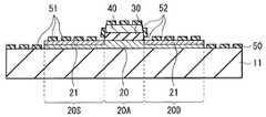
도 7은 제1 변형예에 따른 박막 트랜지스터(1A)의 단면 구성을 나타낸 것이다. 박막 트랜지스터(1A)는, 고-저항막(50)을 제공하지 않음으로써 리크 전류를 저감하도록 한 것을 제외하고는, 상술된 제1 실시예에 따른 박막 트랜지스터(1)와 마찬가지의 구성, 작용 및 효과를 갖는다.7 shows a sectional configuration of the
박막 트랜지스터(1A)는, 예를 들어, 이하와 같이 제조될 수 있다. 우선, 상기 제1 실시예와 마찬가지로, 도 2a 내지 도 3b에 나타낸 공정에 의해, 기판(11)상에, 산화물 반도체막(20), 게이트 절연막(30), 게이트 전극(40) 및 금속막(50A)을 형성하고, 금속막(50A)을 열처리하여 저-저항 영역(21) 및 고-저항막(50)을 형성한다. 이후, 도 8a에 나타낸 바와 같이, 에칭에 의해 고-저항막(50)을 제거한다. 여기서, 염소 등을 포함하는 가스를 사용한 건식 에칭법에 의해, 고-저항막(50) 및 완전하게 산화되지 않은 금속막(50A)을 용이하게 제거하는 것이 가능하다. 이후, 도 8b에 나타낸 바와 같이, 제1 실시예와 마찬가지로, 층간 절연막(60)을 형성한다. 이후, 도 8c에 나타낸 바와 같이, 제1 실시예와 마찬가지로, 층간 절연막(60)에 접속 구멍들을 제공하고, 소스 전극(70S) 및 드레인 전극(70D)을 저-저항 영역(21)에 접속한다.The
[제3 실시예][Third Embodiment]
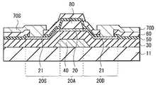
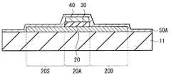
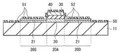
도 9는, 제3 실시예에 따른 박막 트랜지스터(1B)의 단면 구성을 나타낸 것이다. 박막 트랜지스터(1B)가, 기판(11) 상에, 게이트 전극(40), 게이트 절연막(30), 산화물 반도체막(20), 채널 보호막(80), 층간 절연막(60), 소스 전극(70S) 및 드레인 전극(70D)을 이 순서대로 적층한 보텀 게이트 박막 트랜지스터인 것을 제외하고, 박막 트랜지스터(1B)는 상술된 제1 실시예에 따른 박막 트랜지스터(1)와 마찬가지의 구성을 갖는다. 제1 실시예와 동일하거나 동등한 구성 요소에 대해서는 동일한 참조 번호로 나타내며, 상세히 설명하지 않는다는 것을 주목해야 한다.Fig. 9 shows a sectional configuration of the
채널 보호막(80)은, 산화물 반도체막(20)의 채널 영역(20A) 상에 제공된다. 채널 보호막(80)은, 예를 들어, 두께가 200nm 정도이며, 실리콘 산화막, 실리콘 질화막, 산화 알루미늄 막 또는 다른 적절한 막의 단층막 또는 이들의 적층막으로 구성될 수 있다.The channel
박막 트랜지스터(1B)는, 예를 들어 이하와 같이 제조될 수 있다. 제1 실시예와 동일한 공정에 대해서는 제1 실시예를 참조하여 설명한다.The
우선, 기판(11) 상의 전체면에, 스퍼터링법 및 성막법 등을 사용하여, 몰리브덴(Mo) 막 또는 다른 적절한 막으로 이루어지는 막을, 예를 들어 200nm 정도의 두께로 형성한다. 몰리브덴 막을, 예를 들어 포토리소그래피법을 사용해서 패터닝 함으로써, 도 10a에 나타낸 바와 같이, 게이트 전극(40)을 형성한다.First, on the entire surface of the
이후, 도 10a에 나타낸 바와 같이, 게이트 전극(40)을 형성한 기판(11)의 전체면에, 예를 들어 플라즈마 CVD법에 의해, 실리콘 산화막, 산화 알루미늄 막 또는 다른 적절한 막으로 이루어질 수 있는 게이트 절연막(30)을, 300nm 정도의 두께로 형성한다.10A, on the entire surface of the
이후, 도 10b에 나타낸 바와 같이, 게이트 절연막(30) 상에, 제1 실시예와 마찬가지로, 산화물 반도체막(20)을 형성한다.Then, as shown in Fig. 10B, the
이후, 산화물 반도체막(20) 및 게이트 절연막(30)의 전체면에, 실리콘 산화막, 실리콘 질화막, 산화 알루미늄 막 또는 다른 적절한 막의 단층막 또는 적층막으로 이루어질 수 있는 채널 보호 재료막을, 200nm 정도의 두께로 형성한다. 이후, 게이트 전극(40)을 마스크로 하는 이면 노광에 의해, 도 10c에 나타낸 바와 같이, 셀프 얼라인 방식으로 게이트 전극(40)에 가까운 위치에 채널 보호막(80)을 형성한다.Thereafter, a channel protecting material film, which may be a single layer film or a lamination film of a silicon oxide film, a silicon nitride film, an aluminum oxide film, or another suitable film, is formed on the entire surface of the
채널 보호막(80)을 형성한 후에, 도 10d에 나타낸 바와 같이, 산화물 반도체막(20) 및 채널 보호막(80) 상에, 제1 실시예와 마찬가지로, 금속막(50A)을 형성한다.10D, a
이후, 도 11a에 나타낸 바와 같이, 열처리에 의해, 금속막(50A)을 산화시켜 고-저항막(50)을 형성하고, 소스 영역(20S) 및 드레인 영역(20D) 각각의 상면으로부터 깊이 방향으로 연장하는 소스 영역(20S) 및 드레인 영역(20D) 각각의 일부에, 채널 영역(20A)보다도 산소 농도가 낮은 저-저항 영역(21)을 형성한다.Thereafter, as shown in Fig. 11A, the
저-저항 영역(21) 및 고-저항막(50)을 형성한 후에, 도 11b에 나타낸 바와 같이, 제1 실시예와 마찬가지로, 고-저항막(50) 상에 층간 절연막(60)을 형성한다.After formation of the low-
층간 절연막(60)을 형성한 후에, 도 11c에 나타낸 바와 같이, 제1 실시예와 마찬가지로, 층간 절연막(60) 및 고-저항막(50)의 각각에 접속 구멍을 설치하고, 소스 전극(70S) 및 드레인 전극(70D)을 저-저항 영역(21)에 접속한다. 이상에 의해, 도 9에 나타낸 박막 트랜지스터(1B)가 완성된다.After forming the
제3 실시예에 따른 박막 트랜지스터(1B)의 작용 및 효과는 제1 실시예와 마찬가지이다.The operation and effects of the
[제2 변형예][Second Modification]
도 12는, 제2 변형예에 따른 박막 트랜지스터(1C)의 단면 구성을 나타낸 것이다. 박막 트랜지스터(1C)는, 고-저항막(50)을 제공하지 않음으로써 리크 전류를 저감하도록 한 것을 제외하고는, 상술된 제3 실시예에 따른 박막 트랜지스터(1B)와 마찬가지의 구성, 작용 및 효과를 갖는다.12 shows a sectional configuration of the
박막 트랜지스터(1C)는, 예를 들어, 이하와 같이 제조될 수 있다. 우선, 제3 실시예와 마찬가지로, 도 10a 내지 도 10d에 나타낸 공정에 의해, 기판(11) 상에, 게이트 전극(40), 게이트 절연막(30), 산화물 반도체막(20), 채널 보호막(80) 및 금속막(50A)을 형성하고, 금속막(50A)을 열처리하여 저-저항 영역(21) 및 고-저항막(50)을 형성한다. 이후, 도 13a에 나타낸 바와 같이, 에칭에 의해 고-저항막(50)을 제거한다. 이후, 도 13b에 나타낸 바와 같이, 제3 실시예와 마찬가지로, 층간 절연막(60)을 형성한다. 이후, 도 13c에 나타낸 바와 같이, 제3 실시예와 마찬가지로, 층간 절연막(60)에 접속 구멍들을 제공하고, 소스 전극(70S) 및 드레인 전극(70D)을 저-저항 영역(21)에 접속한다.The
[제4 실시예][Fourth Embodiment]
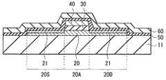
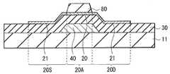
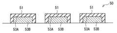
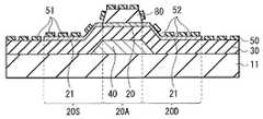
도 14는, 제4 실시예에 따른 박막 트랜지스터(1D)의 구조를 나타낸 것이다. 박막 트랜지스터(1D)는, 고-저항막(50)이 복수의 불연속인 섬 형상의 고-저항막(51)으로 구성되는 것을 제외하고는, 상술된 제1 실시예에 따른 박막 트랜지스터(1)와 마찬가지의 구성을 갖는다. 따라서, 제1 실시예와 동일하거나 동등한 구성요소에 대해서는 동일한 참조 번호로 나타내고, 상세히 설명하지 않는다는 것을 주목해야 한다.Fig. 14 shows the structure of the
각각의 섬 형상의 고-저항막(51)은, 예를 들어, 산화 알루미늄에 의해 구성되어 있다. 여기서, 섬 형상의 고-저항막(51)은, 반드시 두께 방향의 전체가 산화 알루미늄에 의해 구성될 필요는 없다. 예를 들어, 섬 형상의 고-저항막(51)은, 도 15에 나타낸 바와 같이, 이의 상면만이 산화 알루미늄으로 구성되는 산화부(53A)가 되므로, 상기 상면 이외의 부분(하부)은 금속 알루미늄으로 구성되는 미산화부(53B)이여도 좋다. 대안으로서, 섬 형상의 고-저항막(51)은, 도 16에 나타낸 바와 같이, 이의 상면 및 측면이 각각 산화 알루미늄으로 이루어지는 산화부(53A)이며, 상기 상면 및 측면 이외의 부분(중심부)은 금속 알루미늄으로 이루어지는 미산화부(53B)이여도 좋다.Each island-shaped high-
인접하는 섬 형상의 고-저항막(51)의 사이에는 간극(52)이 존재한다. 이 간극(52)에 의해 인접하는 섬 형상의 고-저항막(51)은 물리적으로 서로 분리되어, 각각의 섬 형상의 고-저항막(51)은 인접하는 섬 형상의 고-저항막(51)이 2차원적으로 서로 연결되지 않는 섬 형상의 구조로 되어 있다. 그로 인해, 섬 형상의 고-저항막(51)끼리는 면내 방향으로 전기가 도통되지 않아, 게이트 전극(40)으로부터 소스 전극(70S) 또는 게이트 전극(40)으로부터 드레인 전극(70D)으로 전류 리크를 차단하는 것이 가능해진다. 섬 형상의 고-저항막(51) 및 간극(52)의 평면 형상은 특별히 한정되지 않는다. 섬 형상의 고-저항막(51) 및 간극(52)은 각각 불규칙한 평면 형상이여도 좋다.There is a
복수의 섬 형상의 고-저항막(51)은, 게이트 전극(40)과 산화물 반도체막(20)과의 사이(게이트 절연막(30)의 측면)의 적어도 한 곳에서, 간극(52)에 의해 서로 분리되어 있는 것이 바람직하다. 바꿔 말하면, 섬 형상의 고-저항막(51)의 가장 긴 변은 게이트 절연막(30)의 두께보다 길이가 짧은 것이 바람직하다. 이는 후술하는 제조 공정에서 섬 형상의 금속막(51A)이 완전하게 산화되지 않아, 섬 형상의 고-저항막(51)의 내부에 금속으로 구성되는 미산화부(53B)가 잔존하는 경우에, 섬 형상의 고-저항막(51)의 미산화부(53B)가 게이트 전극(40)의 측면과 저-저항 영역(21)의 상면의 양쪽에 접촉함으로써, 게이트 전극(40)과 소스 전극(70S) 또는 게이트 전극(40)과 드레인 전극(70D)의 사이에서 단락이 발생될 우려를 방지한다.The plurality of island-shaped high-
박막 트랜지스터(1D)는, 예를 들어 이하와 같이 제조될 수 있다.The
도 18a 내지 도 18c는 도 14에 나타낸 박막 트랜지스터(1D)의 제조 방법을 공정순으로 나타낸 것이다. 또한, 제1 실시예와 동일한 공정에 대해서는 도 2a 내지 도 2c를 참조하여 설명한다는 것에 주목해야 한다.Figs. 18A to 18C show the manufacturing method of the
우선, 제1 실시예와 마찬가지로, 도 2a에 나타낸 공정에 의해 산화물 반도체막(20)을 형성한다. 이후, 제1 실시예와 마찬가지로, 도 2b 및 도 2c에 나타낸 공정에 의해, 산화물 반도체막(20)의 채널 영역(20A) 상에 게이트 절연막(30) 및 게이트 전극(40)을 이 순서대로 동일 형상으로 형성한다.First, similarly to the first embodiment, the
이후, 도 18a에 나타낸 바와 같이, 산화물 반도체막(20), 게이트 절연막(30) 및 게이트 전극(40)의 표면에, 알루미늄(Al)으로 이루어지는 복수의 섬 형상의 금속막(51A)으로 구성되는 금속막(50A)을 형성한다. 도 19a는, 복수의 섬 형상의 금속막(51A)으로 구성되는 금속막(50A)를 확대해서 개략적으로 나타낸 것이다. 복수의 섬 형상의 금속막(51A)의 사이에는 간극(52)이 발생한다.18A, a plurality of island-shaped
금속막(50A)의 형성 방법으로서는 진공 성막법 및 스퍼터링법과 같은 방법이 적합하다. 복수의 섬 형상의 금속막(51A)으로 구성되는 금속막(50A)를 형성하는 방법으로서 가장 적합한 것은 스퍼터링법이다. 도 20은 스퍼터링법에서의 손톤 모델(Thornton's model)을 나타내며, 여기서, T는 기판 온도이며, Tm은 재료의 융점이다. 스퍼터링법에서는, 기판의 온도 및 스퍼터링 가스로 역할하는 아르곤(Ar)의 압력을 변화시킴으로써, 형성되는 막의 결정성 및 입경 분포에 차이가 발생한다. T/Tm이 크고, 아르곤의 압력이 낮은 경우, 즉 스퍼터링되는 입자의 에너지가 지극히 크고, 또한 기판상에서 금속막이 움직이기 쉬운 조건의 경우에는, "ZONE3"라 칭하는 상태가 되어, 지극히 치밀한 막이 형성된다. 한편, T/Tm이 작고, 아르곤의 압력이 높은 조건의 경우에는, "ZONE1"라 칭하는 상태가 된다. "ZONE1"의 상태에서는, 막을 매우 두껍게 해도 거친(rough) 상태이다. 즉, 초기 형성 과정에서는 섬 형상의 막을 형성하는 것이 가능해진다. 따라서, 금속막(50A)을 성막할 때에, 기판 온도 및 아르곤의 압력을 적절하게 조정함으로써, 복수의 섬 형상의 금속막(51A)으로 구성되는 금속막(50A)을 형성하는 것이 가능하다.As the method for forming the
이후, 도 18b에 나타낸 바와 같이, 제1 실시예와 마찬가지로 열처리를 행함으로써, 금속막(50A)의 복수의 섬 형상의 금속막(51A)이 산화되어, 산화 알루미늄으로 구성되는 복수의 섬 형상의 고-저항막(51)을 갖는 고-저항막(50)이 형성된다. 이와 함께, 소스 영역(20S) 및 드레인 영역(20D)의 상면으로부터 깊이 방향으로 연장하는 소스 영역(20S) 및 드레인 영역(20D) 각각의 일부에, 알루미늄을 도펀트로서 포함하거나 채널 영역(20A)보다도 산소 농도가 낮은 저-저항 영역(21)이 형성된다.Thereafter, as shown in Fig. 18B, by performing the heat treatment in the same manner as in the first embodiment, a plurality of island-shaped
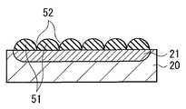
도 19b는, 금속막(50A)의 산화를 확대해서 개략적으로 나타낸 것이다. 금속막(50A)의 복수의 섬 형상의 금속막(51A)은, 분위기 중의 산소 O2 및 하지층으로서 역할하는 산화물 반도체막(20) 내의 산소 O를 흡수하여 산화된다. 여기서, 각각의 섬 형상의 금속막(51A)은 흡수된 산소의 양에 따라 체적이 증대한다. 또한, 복수의 섬 형상의 금속막(51A)으로 구성되는 금속막(50A)은, 산소와 접촉하는 표면적이 커진다. 따라서, 보다 산화가 진행하기 쉬워져, 이 점으로부터도 리크를 억제하는 것이 가능해진다. 한편, 산화물 반도체막(20)에서는, 각각의 섬 형상의 금속막(51A)의 바로 아래에 저-저항 영역(21)이 형성된다.Fig. 19B is an enlarged schematic representation of the oxidation of the
도 19c는, 금속막(50A)의 산화에 의해, 복수의 섬 형상의 고-저항막(51)으로 구성되는 고-저항막(50)이 형성되며, 산화물 반도체막(20)에 저-저항 영역(21)이 형성된 상태를 확대해서 개략적으로 나타낸 것이다. 섬 형상의 고-저항막(51)은 산화에 의해 팽창하는 한편, 간극(52)은 축소한다. 그로 인해, 섬 형상의 고-저항막(51) 중에는, 간극(52)에 의해 인접하는 섬 형상의 고-저항막(51)과 이격되는 섬 형상의 고-저항막(51)이 있을 수 있으며, 간극(52)이 소실해서 인접하는 섬 형상의 고-저항막(51)과 연결되는 섬 형상의 고-저항막(51)도 존재할 수 있다.19C shows a state in which a high-
저-저항 영역(21)을 형성한 후에, 제1 실시예와 마찬가지로, 도 18c에 나타낸 바와 같이, 고-저항막(50) 상에 층간 절연막(60)을 형성한다. 이후, 도 14에 나타낸 바와 같이, 예를 들어 포토리소그래피 및 에칭에 의해 층간 절연막(60)에 접속 구멍들을 형성한다.After forming the low-
이후, 층간 절연막(60)의 상에, 예를 들어 스퍼터링법에 의해, 몰리브덴(Mo) 막 또는 다른 적절한 막을 200nm 정도의 두께로 형성하고, 포토리소그래피 및 에칭에 의해 미리 정해진 형상으로 성형한다. 이에 의해, 도 14에 나타낸 바와 같이, 소스 전극(70S) 및 드레인 전극(70D)을 저-저항 영역(21)에 접속한다.Thereafter, a molybdenum (Mo) film or another suitable film is formed on the
도 19d는 복수의 섬 형상의 고-저항막(51) 상에 소스 전극(70S) 및 드레인 전극(70D)을 형성한 상태를 나타낸 것이다. 복수의 섬 형상의 고-저항막(51)은 간극(52)에 의해 서로 분리되어 있으므로, 이 간극(52)을 통하여 소스 전극(70S) 및 드레인 전극(70D)이 저-저항 영역(21)과 접속된다. 따라서, 소스 전극(70S)과 저-저항 영역(21)과의 콘택트 저항 및 드레인 전극(70D)과 저-저항 영역(21)과의 콘택트 저항이 작아져, 저-저항 영역(21) 상의 섬 형상의 고-저항막(51)을 제거하는 공정이 불필요하게 된다. 이상에 의해, 도 14에 나타낸 박막 트랜지스터(1D)가 완성된다.19D shows a state in which a
이러한 박막 트랜지스터(1D)에서는, 제1 실시예와 마찬가지로, 게이트 전극(40)에 미리 정해진 임계치 전압 이상의 전압(게이트 전압)이 인가되면, 산화물 반도체막(20)의 채널 영역(20A) 내에 전류(드레인 전류)가 발생한다. 여기에서는, 고-저항막(50)이 복수의 불연속인 섬 형상의 고-저항막(51)에 의해 구성되며, 인접하는 섬 형상의 고-저항막(51)은 간극(52)에 의해 물리적으로 서로 분리되어 있다. 따라서, 섬 형상의 고-저항막(51)끼리는 전기가 도통되지 않는다. 따라서, 게이트 전극(40)으로부터 소스 전극(70S) 또는 게이트 전극(40)으로부터 드레인 전극(70D)으로 전류 리크가 차단되어, 트랜지스터 특성이 향상된다.In this
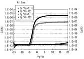
도 21a는, 상술한 제조 방법에 의해, 복수의 섬 형상의 고-저항막(51)으로 구성되는 고-저항막(50)을 갖는 실제로 제작된 박막 트랜지스터(1D)의 특성을 조사한 결과를 나타낸 것이다. 여기서, 우선, 유리 기판으로 이루어진 기판(11) 상에 버퍼층으로서 PECVD(plasma-enhanced chemical vapor deposition) 법에 의해 두께 200nm의 산화 실리콘(SiO2)막을 형성하였다. 이후, 두께 40nm의 InGaZnO막으로 이루어지는 산화물 반도체막(20)을 형성하였다. 이후, 두께 5nm의 알루미늄 막으로 이루어지는 금속막(50A)을 형성하였다. 금속막(50A)의 성막 조건은, 기판 온도 약 100℃, 아르곤 압력 약 0.5Pa이다. 이 경우, 알루미늄의 융점은 660℃ 정도이기 때문에, T/Tm = 0.15가 된다. 아르곤 압력이 낮으므로, 도 20에 나타낸 손톤 모델에서의 "ZONE T(transition)"에서 성막되었을 가능성이 높았다. 그러나, 성막 후의 금속막(50A)의 단면을 조사한 바, 복수의 불연속인 섬 형상의 금속막(51A)이 형성되어 있는 것이 확인되었다. 또한, 아르곤 압력을 좀더 높게 하는 것으로 "ZONE1"에서의 성막이 가능해지고, 금속막(50A)의 두께를 두껍게 하는 것이 가능해졌다고 생각된다. 이후, 금속막(50A)에 대한 열처리로서, 약 30%의 산소 분위기하에서, 300℃로 1시간 동안 어닐링을 행함으로써 저-저항 영역(21)을 형성하였다.21A shows a result of examining the characteristics of a
한편, 금속막의 형성 및 열처리를 행하지 않고 다른 박막 트랜지스터를 제작하여, 트랜지스터 특성을 조사하였고, 그 결과를 도 21b에 나타낸다.On the other hand, another thin film transistor was fabricated without forming a metal film and heat treatment, and the transistor characteristics were examined. The results are shown in Fig. 21B.
도 21a 및 도 21b로부터 알 수 있는 바와 같이, 복수의 섬 형상의 금속막(51A)으로 구성되는 금속막(50A)의 열처리에 의해, 저-저항 영역(21)을 형성하고 복수의 섬 형상의 고-저항막(51)으로 구성되는 고-저항막(50)을 형성한 박막 트랜지스터(1D)에서는, 금속막의 형성 및 열처리를 행하지 않은 박막 트랜지스터에 비하여, 트랜지스터의 온 전류가 두자리 이상 증가되었다. 즉, 고-저항막(50)이 복수의 섬 형상의 고-저항막(51)으로 구성되는 박막 트랜지스터(1D)라 하더라도, 제1 실시예와 마찬가지로, 셀프 얼라인 구조에 의해 기생 용량을 저감함과 함께 소자 특성이 안정된 박막 트랜지스터(1D)를 실현할 수 있는 것을 알았다.As can be seen from Figs. 21A and 21B, the low-
도 22a 및 도 22b는, 금속막(50A)의 두께를 5nm 또는 10nm로 변화시킴으로써, 고-저항막(50)의 두께가 상이한 박막 트랜지스터(1D)를 제작하고, 박막 트랜지스터(1D)에 대해서, 소스-드레인 전류(Id) 및 게이트-드레인 전류(Ig)를 조사한 결과를 나타낸 것이다. 도 22a 및 도 22b로부터 알 수 있는 바와 같이, 금속막(50A)의 두께를 10nm로 한 박막 트랜지스터(1D)의 경우에는, 금속막(50A)의 두께를 5nm로 한 박막 트랜지스터(1D)의 경우에 비해서 트랜지스터의 오프 시의 전류가 크므로, 소스 전극(70S)과 드레인 전극(70D)과의 연결이 시사되어 있다. 또한, 10nm의 금속막(50A) 두께를 가지는 박막 트랜지스터(1D)에서는, Ig로 나타낸 리크 전류가 상당히 크므로, 이는 고-저항막(50)이 리크 패스(leakage path)로 역할한다는 것이 명확하다. 즉, 금속막(50A)을 5nm 이하의 두께로 형성함으로써, 리크를 저감하여, 트랜지스터 특성을 향상시킬 수 있다는 것을 알았다.22A and 22B show a case where a
제4 실시예에 따르면, 고-저항막(50)이 복수의 섬 형상의 고-저항막(51)에 의해 구성된다. 따라서, 제1 실시예의 효과에 부가하여, 리크 전류를 저감하고, 트랜지스터 특성을 향상시킬 수 있다. 또한, 소스 전극(70S)과 저-저항 영역(21)과의 콘택트 저항 및 드레인 전극(70D)과 저-저항 영역(21)과의 콘택트 저항을 저감함으로써, 저-저항 영역(21) 상의 섬 형상의 고-저항막(51)을 제거하는 공정이 불필요하게 된다. 따라서, 제조 공정이 간소화된다.According to the fourth embodiment, the high-
[제3 변형예][Third Modification]
도 23a 내지 도 24b는 제3 변형예에 따른 박막 트랜지스터(1D)의 제조 방법을 공정순으로 나타낸 것이다. 이러한 변형예에 따른 제조 방법은 상술된 제4 실시 예와는 고-저항막(50)을 형성하는 방법이 다른 것이다. 또한, 제1 실시예와 대응되는 제조 공정에 대해서는, 도 2a 내지 도 2c를 참조하여 설명한다는 것을 주목해야 한다.23A to 24B show the manufacturing method of the
우선, 제1 실시예와 마찬가지로, 도 2a에 나타낸 공정에 의해, 산화물 반도체막(20)을 형성한다. 이후, 제1 실시예와 마찬가지로, 도 2b 및 도 2c에 나타낸 공정에 의해, 산화물 반도체막(20)의 채널 영역(20A) 상에 게이트 절연막(30) 및 게이트 전극(40)을 이 순서대로 동일 형상으로 형성한다.First, similarly to the first embodiment, the
이후, 도 23a에 나타낸 바와 같이, 산화물 반도체막(20), 게이트 절연막(30) 및 게이트 전극(40)의 표면에, 알루미늄(Al)으로 구성되는 금속막(50A)을, 균일한 연속막으로서 형성한다.23A, a
이후, 도 23b에 나타낸 바와 같이, 예를 들어 포토리소그래피 및 에칭 공정에 의해 금속막(50A)을 패터닝함으로써, 금속막(50A)을 복수의 섬 형상의 금속막(51A)으로 분할한다. 복수의 섬 형상의 금속막(51A)의 사이에는 간극(52)을 설치하고, 이 간극(52)을 이용하여 복수의 섬 형상의 금속막(51A)을 서로 물리적으로 분리한다.Thereafter, as shown in Fig. 23B, the
복수의 섬 형상의 금속막(51A)을 형성한 후에, 도 24a에 나타낸 바와 같이, 제1 실시예와 마찬가지로 열처리를 행함으로써, 금속막(50A)의 복수의 섬 형상의 금속막(51A)이 산화되어, 산화 알루미늄으로 구성되는 복수의 섬 형상의 고-저항막(51)을 갖는 고-저항막(50)이 형성된다. 이와 함께, 소스 영역(20S) 및 드레인 영역(20D)의 상면으로부터 깊이 방향으로 연장하는 소스 영역(20S) 및 드레인 영역(20D) 각각의 일부에, 알루미늄을 도펀트로서 포함하거나 채널 영역(20A)보다도 산소 농도가 낮은 저-저항 영역(21)이 형성된다.After the formation of a plurality of island-shaped
저-저항 영역(21)을 형성한 후에, 제1 실시예와 마찬가지로, 도 24b에 나타낸 바와 같이, 고-저항막(50) 상에 층간 절연막(60)을 형성한다. 이후, 도 14에 나타낸 바와 같이, 예를 들어 포토리소그래피 및 에칭에 의해 층간 절연막(60)에 접속 구멍들을 형성한다.After forming the low-
이후, 층간 절연막(60)의 상에, 예를 들어 스퍼터링법에 의해, 몰리브덴(Mo) 막 또는 다른 적절한 막을 200nm 정도의 두께로 형성하고, 포토리소그래피 및 에칭에 의해 미리 정해진 형상으로 성형한다. 이에 의해, 도 14에 나타낸 바와 같이, 소스 전극(70S) 및 드레인 전극(70D)을 저-저항 영역(21)에 접속한다. 복수의 섬 형상의 고-저항막(51)은 간극(52)에 의해 서로 분리되어 있으므로, 이 간극(52)을 통하여 소스 전극(70S)과 드레인 전극(70D)이 저-저항 영역(21)과 접속된다. 따라서, 소스 전극(70S)과 저-저항 영역(21)과의 콘택트 저항 및 드레인 전극(70D)과 저-저항 영역(21)과의 콘택트 저항이 작아져, 저-저항 영역(21) 상의 섬 형상의 고-저항막(51)을 제거하는 공정이 불필요하게 된다. 이상에 의해, 도 14에 나타낸 박막 트랜지스터(1D)가 완성된다.Thereafter, a molybdenum (Mo) film or another suitable film is formed on the
[제4 변형예][Fourth Modification]
도 25a 내지 도 26b는 제4 변형예에 따른 박막 트랜지스터(1D)의 제조 방법을 공정순으로 나타낸 것이다. 이러한 변형예에 따른 제조 방법은 상술된 제4 실시예와는 고-저항막(50)을 형성하는 방법이 다른 것이다. 제1 실시예와 대응하는 제조 공정에 대해서는, 도 2a 내지 도 2c를 참조하여 설명한다는 것을 주목해야 한다.25A to 26B show a manufacturing method of the
우선, 제1 실시예와 마찬가지로, 도 2a에 나타낸 공정에 의해, 산화물 반도체막(20)을 형성한다. 이후, 제1 실시예와 마찬가지로, 도 2b 및 도 2c에 나타낸 공정에 의해, 산화물 반도체막(20)의 채널 영역(20A) 상에 게이트 절연막(30) 및 게이트 전극(40)을 이 순서대로 동일 형상으로 형성한다.First, similarly to the first embodiment, the
이후, 도 25a에 나타낸 바와 같이, 산화물 반도체막(20), 게이트 절연막(30) 및 게이트 전극(40)의 표면에, 알루미늄(Al)으로 구성되는 금속막(50A)을, 균일한 연속막으로서 형성한다.25A, a
이후, 도 25b에 나타낸 바와 같이, 제1 실시예와 마찬가지로 열처리를 행함으로써, 금속막(50A)이 산화되어 고-저항막(50)이 형성된다. 이와 함께, 소스 영역(20S) 및 드레인 영역(20D)의 상면으로부터 깊이 방향으로 연장하는 소스 영역(20S) 및 드레인 영역(20D) 각각의 일부에, 알루미늄을 도펀트로서 포함하거나 채널 영역(20A)보다도 산소 농도가 낮은 저-저항 영역(21)이 형성된다.Thereafter, as shown in Fig. 25B, the
이후, 도 26a에 나타낸 바와 같이, 예를 들어 포토리소그래피 및 에칭 공정에 의해 고-저항막(50)을 패터닝 함으로써, 고-저항막(50)을 복수의 섬 형상의 고-저항막(51)으로 분할한다. 복수의 섬 형상의 고-저항막(51)의 사이에는 간극(52)이 설치되고, 이 간극(52)을 이용하여 복수의 섬 형상의 고-저항막(51)을 서로 물리적으로 분리한다.Thereafter, as shown in Fig. 26A, the high-
복수의 섬 형상의 고-저항막(51)을 형성한 후에, 제1 실시예와 마찬가지로, 도 26b에 나타낸 바와 같이, 고-저항막(50) 상에 층간 절연막(60)을 형성한다. 이후, 도 14에 나타낸 바와 같이, 예를 들어 포토리소그래피 및 에칭 공정에 의해 층간 절연막(60)에 접속 구멍들을 형성한다.After forming a plurality of island-shaped high-
이후, 층간 절연막(60)의 상에, 예를 들어 스퍼터링법에 의해, 몰리브덴(Mo) 막 또는 다른 적절한 막을 200nm 정도의 두께로 형성하고, 포토리소그래피 및 에칭 공정에 의해 미리 정해진 형상으로 성형한다. 이에 의해, 도 14에 나타낸 바와 같이, 소스 전극(70S) 및 드레인 전극(70D)을 저-저항 영역(21)에 접속한다. 복수의 섬 형상의 고-저항막(51)은 간극(52)에 의해 서로 분리되어 있으므로, 이 간극(52)을 통하여 소스 전극(70S)과 드레인 전극(70D)이 저-저항 영역(21)에 접속된다. 따라서, 소스 전극(70S)과 저-저항 영역(21)과의 콘택트 저항 및 드레인 전극(70D)과 저-저항 영역(21)과의 콘택트 저항이 작아져, 저-저항 영역(21) 상의 섬 형상의 고-저항막(51)을 제거하는 공정이 불필요하게 된다. 이상에 의해, 도 14에 나타낸 박막 트랜지스터(1D)가 완성된다.Thereafter, a molybdenum (Mo) film or another suitable film is formed on the
[제5 실시예][Fifth Embodiment]
도 27은 제5 실시예에 따른 박막 트랜지스터(1E)의 단면 구조를 나타낸 것이다. 박막 트랜지스터(1E)가 기판(11) 상에, 게이트 전극(40), 게이트 절연막(30), 산화물 반도체막(20), 채널 보호막(80), 층간 절연막(60), 소스 전극(70S) 및 드레인 전극(70D)을 이 순서대로 적층한 보텀 게이트 박막 트랜지스터라는 점을 제외하고, 박막 트랜지스터(1E)는 상술된 제3 및 제4 실시예에 따른 각각의 박막 트랜지스터(1B 및 1D)와 마찬가지의 구성을 갖는다. 제3 및 제4 실시예와 동일하거나 동등한 구성 요소에 대해서는 동일한 참조 번호로 나타내며, 상세히 설명하지 않는다는 것을 주목해야 한다.FIG. 27 shows a cross-sectional structure of the
박막 트랜지스터(1E)는, 예를 들어 이하와 같이 제조될 수 있다. 또한, 제1 또는 제3 실시예와 동일한 공정에 대해서는 제1 또는 제3 실시예를 참조하여 설명한다는 것을 주목해야 한다.The
우선, 제3 실시예와 마찬가지로, 도 10a에 나타낸 공정에 의해, 도 28a에 나타낸 바와 같이, 기판(11) 상에 게이트 전극(40)과 게이트 절연막(30)을 이 순서대로 형성한다.First, as in the third embodiment, the
이후, 제3 실시예와 마찬가지로, 도 10b에 나타낸 공정에 의해, 도 28b에 나타낸 바와 같이 게이트 절연막(30) 상에 산화물 반도체막(20)을 형성한다.Thereafter, as in the third embodiment, the
이후, 제3 실시예와 마찬가지로, 도 10c에 나타낸 공정에 의해 도 28c에 나타낸 바와 같이 산화물 반도체막(20) 상에 채널 보호막(80)을 형성한다.Thereafter, as in the third embodiment, the channel
이후, 제4 실시예와 마찬가지로, 도 18a에 나타낸 공정에 의해, 도 28d에 나타낸 바와 같이 산화물 반도체막(20), 채널 보호막(80) 및 게이트 절연막(30) 상에 복수의 섬 형상의 금속막(51A)으로 구성되는 금속막(50A)을 형성한다.Thereafter, as shown in Fig. 28 (d), a plurality of island-like metal films (not shown) are formed on the
이후, 제4 실시예와 마찬가지로, 도 18b에 나타낸 공정에 의해, 도 29a에 나타낸 바와 같이 열처리에 의해 금속막(50A)의 복수의 섬 형상의 금속막(51A)을 산화시켜, 복수의 섬 형상의 고-저항막(51)으로 구성되는 고-저항막(50)을 형성한다. 이와 함께, 소스 영역(20S) 및 드레인 영역(20D)의 상면으로부터 깊이 방향으로 연장하는 소스 영역(20S) 및 드레인 영역(20D) 각각의 일부 또는 전체에, 채널 영역(20A)보다도 산소 농도가 낮은 저-저항 영역(21)을 형성한다.Thereafter, as shown in Fig. 29A, the island-shaped
저-저항 영역(21) 및 고-저항막(50)을 형성한 후에, 도 29b에 나타낸 바와 같이, 제1 실시예와 마찬가지로, 고-저항막(50) 상에 층간 절연막(60)을 형성한다.After forming the low-
층간 절연막(60)을 형성한 후에, 도 29c에 나타낸 바와 같이, 제1 실시예와 마찬가지로 층간 절연막(60)에 접속 구멍들을 설치하고, 소스 전극(70S) 및 드레인 전극(70D)을 저-저항 영역(21)에 접속한다. 이상에 의해, 도 27에 나타낸 박막 트랜지스터(1E)가 완성된다.After forming the
[제1 적용예][First Application Example]
도 30은, 박막 트랜지스터들(1 내지 1E) 중의 임의의 하나를 구동 소자로서 구비한 디스플레이 장치(90)의 회로 구성을 나타내는 것이다. 디스플레이 장치(90)는, 예를 들어 액정 디스플레이 및 유기 EL 디스플레이 등의 디스플레이일 수 있다. 디스플레이 장치(90)는 구동 패널(91) 상에 매트릭스 형상으로 배치된 복수의 화소(10R, 10G, 10B)와, 이들의 화소(10R, 10G, 10B)를 구동시키기 위한 각종 구동 회로가 제공된 것이다. 화소(10R, 10G, 10B)는 각각 적색(R: Red), 녹색(G: Green) 및 청색(B: Blue)의 색을 발광하는 액정 디스플레이 소자 및 유기 EL 소자 등의 소자일 수 있으며, 색의 수 및 종류는 이들 색상으로 제한되지 않는다. 그래서, 이들 3개의 화소(10R, 10G, 10B)를 하나의 픽셀로서 집합하여 복수의 픽셀을 가지는 디스플레이 영역(110)이 구성된다. 구동 패널(91) 위에는, 구동 회로로서, 예를 들어 영상 디스플레이용의 드라이버로서 각각 역할하는 신호선 구동 회로(120) 및 주사선 구동 회로(130)와, 화소 구동 회로(150)가 제공되어 있다. 이 구동 패널(91)에는, 도시하지 않은 밀봉 패널이 부착되어 있어, 이 밀봉 패널에 의해 화소(10R, 10G, 10B) 및 상기 구동 회로가 밀봉되어 있다.30 shows a circuit configuration of a
도 31은 화소 구동 회로(150)의 등가 회로도이다. 화소 구동 회로(150)는 트랜지스터(Tr1 및 Tr2)가 배치된 액티브형의 구동 회로이다. 각각의 트랜지스터(Tr1 및 Tr2)는 상술된 박막 트랜지스터들(1 내지 1E) 중의 임의의 하나이다. 트랜지스터(Tr1 및 Tr2)의 사이에는 캐패시터(Cs)가 제공된다. 제1 전원 라인(Vcc)과 제2 전원 라인(GND)의 사이에는, 화소(10R)(또는 화소(10G 또는 10B))가 트랜지스터(Tr1)에 직렬로 접속되어 있다. 화소 구동 회로(150)에서는, 열 방향으로 신호선(120A)이 더 복수 배치되며, 행 방향으로 주사선(130A)이 더 복수 배치되어 있다. 각각의 신호선(120A)은 신호선 구동 회로(120)에 접속되어, 이 신호선 구동 회로(120)로부터 신호선(120A)을 통해서 트랜지스터(Tr2)의 소스 전극에 회로 화상 신호들이 공급되도록 되어 있다. 각각의 주사선(130A)은 주사선 구동 회로(130)에 접속되어, 이 주사선 구동 회로(130)로부터 주사선(130A)을 통해서 트랜지스터(Tr2)의 게이트 전극에 회로 주사 신호들이 순차적으로 공급되도록 되어 있다. 디스플레이 장치(90)에서는, 각각의 트랜지스터(Tr1 및 Tr2)가 상기 실시예 및 변형예에 따른 박막 트랜지스터(1 내지 1E) 중의 임의의 하나에 의해 구성된다. 따라서, 셀프 얼라인 구조에 의해 기생 용량이 감소되고 특성이 안정된 박막 트랜지스터(1 내지 1E) 중의 임의의 하나에 의해, 고품질의 디스플레이가 가능해진다. 이러한 디스플레이 장치(90)는, 예를 들어 이하의 적용예 2 내지 6에 나타낸 전자 기기에 탑재될 수 있다.Fig. 31 is an equivalent circuit diagram of the
[제2 적용예][Second Application Example]
도 32는 텔레비전 장치의 외관을 나타낸 것이다. 이 텔레비전 장치에는, 예를 들어, 프론트 패널(310) 및 필터 유리(320)를 포함하는 영상 디스플레이 화면부(300)가 제공된다.32 shows the appearance of the television apparatus. In this television apparatus, for example, an image
[제3 적용예][Third Application Example]
도 33a 내지 도 33b는 각각 디지털 스틸 카메라의 외관을 나타낸 것이다. 이 디지털 스틸 카메라에는, 예를 들어, 플래시용의 발광부(410), 디스플레이부(420), 메뉴 스위치부(430) 및 셔터 버튼(440)이 제공된다.33A to 33B show the appearance of a digital still camera, respectively. The digital still camera is provided with, for example, a
[제4 적용예][Fourth application example]
도 34는 노트북형 퍼스널 컴퓨터의 외관을 나타낸 것이다. 이 노트북형 퍼스널 컴퓨터에는, 예를 들어, 본체(510)와, 문자 등의 입력 조작을 위한 키보드(520)와, 화상을 디스플레이하는 디스플레이부(530)가 제공된다.34 shows an appearance of a notebook type personal computer. This notebook type personal computer is provided with, for example, a
[제5 적용예][Application example 5]
도 35는 비디오 카메라의 외관을 나타낸 것이다. 이 비디오 카메라에는, 예를 들어, 본체부(610)와, 본체부(610)의 전방측면에 설치된 피사체 촬영용의 렌즈(620)와, 촬영 시작/정지 스위치(630)와, 디스플레이부(640)가 제공된다.35 shows an appearance of a video camera. The video camera includes a
[제6 적용예][Application example 6]
도 36a 내지 도 36g는 각각 휴대 전화기의 외관을 나타낸 것이다. 이 휴대 전화기는, 예를 들어, 상측 하우징(710)과 하측 하우징(720)을 연결부(또는 힌지부) (730)로 연결한 것이며, 예를 들면 디스플레이(740), 서브 디스플레이(750), 픽처 라이트(picture light; 760) 및 카메라(770)를 갖는다.Figs. 36A to 36G show the appearance of the mobile phone, respectively. The portable telephone is connected to the
이상, 실시예, 변형예 및 적용예를 참조하여 본 출원을 설명했지만, 본 발명은 이들에 한정되는 것이 아니고, 다양한 변형이 가능하다. 예를 들어, 상술된 실시예 등에서는, 저-저항 영역(21)이 소스 영역(20S) 및 드레인 영역(20D) 각각의 상면으로부터 깊이 방향으로 연장하는 소스 영역(20S) 및 드레인 영역(20D) 각각의 일부에 제공되어 있는 경우에 대해서 설명하였다. 그러나, 저-저항 영역(21)은 소스 영역(20S) 및 드레인 영역(20D) 각각의 상면으로부터 깊이 방향으로 연장하는 소스 영역(20S) 및 드레인 영역(20D) 각각의 적어도 일부에 제공되어 있어도 좋다. 예를 들어, 저-저항 영역(21)은, 도 37에 나타낸 바와 같이, 소스 영역(20S) 및 드레인 영역(20D) 각각의 상면으로부터 깊이 방향으로 연장하는 소스 영역(20S) 및 드레인 영역(20D) 각각의 전체에 제공되어 있어도 좋다.Although the present application has been described with reference to the embodiments, modifications, and application examples, the present invention is not limited thereto, and various modifications are possible. For example, in the above-described embodiments and the like, the low-
또한, 상술된 실시예 등에서는, 산화물 반도체막(20)이 기판(11) 상에 직접 제공되어 있다. 그러나, 산화물 반도체막(20)은, 기판(11) 상에 실리콘 이산화막, 실리콘 질화막 및 산화 알루미늄 막 등의 절연막을 사이에 두어도 된다. 이에 의해, 기판(11)으로부터 산화물 반도체막(20) 내로, 불순물 및 수분 등의 영향을 미치는 인자들이 확산하는 것을 억제할 수 있다.In the above-described embodiments and the like, the
상술된 실시예 등에서 여러 층의 재료 및 두께와, 성막 방법과, 성막 조건은 예시를 위한 것이며 한정되는 것이 아니다. 다른 재료, 두께, 성막법 및 성막 조건을 채용해도 좋다.In the above-described embodiments and the like, the materials and thicknesses of the various layers, the film forming method, and the film forming conditions are for the purpose of illustration and are not limitative. Other materials, thicknesses, film forming methods and film forming conditions may be employed.
액정 디스플레이 및 유기 EL 디스플레이 외에, 본 출원은 무기 EL 소자, 전해 석출(electrodeposition)형 디스플레이 소자 및 전기 변색(electrochromic)형 디스플레이 소자 등의 다른 디스플레이 소자를 이용하는 디스플레이 장치에 적용될 수 있다.In addition to liquid crystal displays and organic EL displays, the present application can be applied to display devices using other display devices such as inorganic EL devices, electrodeposition type display devices and electrochromic type display devices.
본 출원은 예시적 실시예 등의 관점에서 설명되었으나, 이러한 실시예 등으로 제한되는 것은 아니다. 당업자라면, 이하의 청구 범위에 의해 규정된 바와 같이, 본 출원의 범위를 벗어남 없이, 상술된 실시예 등에서 변형이 있을 수 있다는 것을 이해할 수 있다. 청구 범위의 한정은 청구 범위에 사용된 언어에 기초하여 광의의 의미로 해석되어야 하며, 본 명세서에 설명되거나 본 출원을 실행하는 동안의 예로 제한되지 않으며, 이 예들은 비-배타적으로 이루어져야 한다. 예컨대, 이러한 개시에 있어서, "바람직한" 등의 용어는 비-배타적인 것으로, "바람직하게"를 의미하는 것이며, 이로써 한정되는 것은 아니다. 제1, 제2 등의 용어를 사용한 것은 임의의 순서 또는 중요도를 나타낸 것이 아니라, 하나의 구성요소를 다른 구성요소와 구별하기 위하여 제1, 제2 등을 사용한 것이다. 또한, 이러한 개시에서의 성분 또는 구성요소 없음(no element or component)은 성분 또는 구성요소가 이하의 청구범위에 명확히 기술되었는지에 관계없이 대중에게 헌정된다는 것을 의도한다.Although the present application has been described in terms of exemplary embodiments and the like, it is not limited to these embodiments and the like. It will be understood by those skilled in the art that variations may be made in the above-described embodiments and the like without departing from the scope of the present application, as defined by the following claims. The scope of the claims should be interpreted broadly on the basis of the language used in the claims, and are not limited to the examples described herein or during the practice of the present application, and these examples should be non-exclusive. For example, in this disclosure, the terms "preferred" and the like are meant to be non-exclusive, and "advantageously " The use of the terms first, second, etc. does not indicate any order or importance, but uses first, second, etc. to distinguish one component from another. Also, no element or component in this disclosure is intended to be dedicated to the public regardless of whether the component or component is specifically described in the following claims.
Claims (4)
Translated fromKorean채널 영역과, 알루미늄, 붕소, 갈륨, 인듐, 티타늄, 실리콘, 게르마늄, 주석, 납 및 이들의 혼합물로 이루어진 군으로부터 선택되는 도펀트를 포함하는 저-저항 영역을 갖는 소스 영역 및 드레인 영역이 형성된 산화물 반도체층과,
상기 산화물 반도체층의 위쪽에 형성된 게이트 절연막 및 게이트 전극과,
상기 저-저항 영역에 접하고, 상기 산화물 반도체층 위에 형성되고, 상기 도펀트로서 선택된 물질의 산화물로 된 고-저항 재료층과,
소스 전극 및 드레인 전극
을 구비하고,
상기 고-저항 재료층은 복수의 섬 형상의 고저항막을 포함하고, 상기 소스 전극 및 드레인 전극은 상기 복수의 섬 형상의 고저항막 사이의 간극을 통해서 상기 저-저항 영역에 전기적으로 접속되는, 박막 트랜지스터.As a thin film transistor,
A semiconductor device comprising an oxide semiconductor having a channel region and a source region and a drain region having a low-resistance region including a dopant selected from the group consisting of aluminum, boron, gallium, indium, titanium, silicon, germanium, tin, lead, Layer,
A gate insulating film and a gate electrode formed above the oxide semiconductor layer,
A high-resistance material layer in contact with the low-resistance region and formed on the oxide semiconductor layer, the high-resistance material layer being made of an oxide of a material selected as the dopant,
The source electrode and the drain electrode
And,
Wherein the high-resistance material layer includes a plurality of island-shaped high-resistance films, and the source electrode and the drain electrode are electrically connected to the low-resistance region through a gap between the plurality of island- Thin film transistor.
상기 복수의 섬 형상의 고저항막은 서로 간극을 제공하도록 이격되어 있는, 박막 트랜지스터.The method according to claim 1,
Wherein the plurality of island-shaped high-resistance films are spaced apart from each other to provide a gap therebetween.
상기 복수의 섬 형상의 고저항막의 제1 부분은 상기 저-저항 영역과 접촉하고, 상기 복수의 섬 형상의 고저항막의 제2 부분은 상기 게이트 전극의 상부와 접촉하는, 박막 트랜지스터.3. The method of claim 2,
Wherein a first portion of the plurality of island-shaped high resistance films contacts the low-resistance region, and a second portion of the plurality of island-shaped high resistance films contacts an upper portion of the gate electrode.
채널 영역과, 알루미늄, 붕소, 갈륨, 인듐, 티타늄, 실리콘, 게르마늄, 주석, 납 및 이들의 혼합물로 이루어진 군으로부터 선택되는 도펀트를 포함하는 저-저항 영역을 갖는 소스 영역 및 드레인 영역이 형성된 산화물 반도체층과,
게이트 전극과,
상기 게이트 전극 및 상기 저-저항 영역에 접하고, 상기 산화물 반도체층 위에 형성된 고-저항 재료층과,
상기 고-저항 재료층에 형성된 접속 구멍을 통해서 상기 저-저항 영역에 전기적으로 접속된 소스 전극 및 드레인 전극
을 구비하고,
상기 고-저항 재료층은 상기 도펀트로서 선택된 물질의 산화물로 되어 있는, 박막 트랜지스터.As a thin film transistor,
A semiconductor device comprising an oxide semiconductor having a channel region and a source region and a drain region having a low-resistance region including a dopant selected from the group consisting of aluminum, boron, gallium, indium, titanium, silicon, germanium, tin, lead, Layer,
A gate electrode,
A high-resistance material layer in contact with the gate electrode and the low-resistance region and formed on the oxide semiconductor layer;
A source electrode and a drain electrode electrically connected to the low-resistance region through a connection hole formed in the high-resistance material layer;
And,
Wherein the high-resistance material layer comprises an oxide of a material selected as the dopant.
Applications Claiming Priority (4)
| Application Number | Priority Date | Filing Date | Title |
|---|---|---|---|
| JP2010079293 | 2010-03-30 | ||
| JPJP-P-2010-079293 | 2010-03-30 | ||
| JPJP-P-2010-245035 | 2010-11-01 | ||
| JP2010245035AJP5708910B2 (en) | 2010-03-30 | 2010-11-01 | THIN FILM TRANSISTOR, MANUFACTURING METHOD THEREOF, AND DISPLAY DEVICE |
Related Parent Applications (1)
| Application Number | Title | Priority Date | Filing Date |
|---|---|---|---|
| KR1020110025260ADivisionKR20110109885A (en) | 2010-03-30 | 2011-03-22 | Thin film transistor, method for manufacturing same, and display device |
Publications (2)
| Publication Number | Publication Date |
|---|---|
| KR20170117928A KR20170117928A (en) | 2017-10-24 |
| KR101847355B1true KR101847355B1 (en) | 2018-04-09 |
Family
ID=44697196
Family Applications (2)
| Application Number | Title | Priority Date | Filing Date |
|---|---|---|---|
| KR1020110025260ACeasedKR20110109885A (en) | 2010-03-30 | 2011-03-22 | Thin film transistor, method for manufacturing same, and display device |
| KR1020170126056AActiveKR101847355B1 (en) | 2010-03-30 | 2017-09-28 | Thin-film transistor, method of manufacturing the same, and display device |
Family Applications Before (1)
| Application Number | Title | Priority Date | Filing Date |
|---|---|---|---|
| KR1020110025260ACeasedKR20110109885A (en) | 2010-03-30 | 2011-03-22 | Thin film transistor, method for manufacturing same, and display device |
Country Status (4)
| Country | Link |
|---|---|
| US (2) | US9859437B2 (en) |
| JP (1) | JP5708910B2 (en) |
| KR (2) | KR20110109885A (en) |
| CN (1) | CN102208452B (en) |
Families Citing this family (153)
| Publication number | Priority date | Publication date | Assignee | Title |
|---|---|---|---|---|
| JP5213421B2 (en)* | 2007-12-04 | 2013-06-19 | キヤノン株式会社 | Oxide semiconductor thin film transistor |
| WO2011145633A1 (en)* | 2010-05-21 | 2011-11-24 | Semiconductor Energy Laboratory Co., Ltd. | Semiconductor device |
| US8519387B2 (en)* | 2010-07-26 | 2013-08-27 | Semiconductor Energy Laboratory Co., Ltd. | Semiconductor device and method for manufacturing |
| WO2012020525A1 (en)* | 2010-08-07 | 2012-02-16 | シャープ株式会社 | Thin-film transistor substrate, and liquid crystal display device provided with same |
| US8797303B2 (en) | 2011-03-21 | 2014-08-05 | Qualcomm Mems Technologies, Inc. | Amorphous oxide semiconductor thin film transistor fabrication method |
| JP5490314B2 (en)* | 2011-04-18 | 2014-05-14 | シャープ株式会社 | Thin film transistor, display panel, and method of manufacturing thin film transistor |
| JP6005401B2 (en)* | 2011-06-10 | 2016-10-12 | 株式会社半導体エネルギー研究所 | Method for manufacturing semiconductor device |
| US8901554B2 (en)* | 2011-06-17 | 2014-12-02 | Semiconductor Energy Laboratory Co., Ltd. | Semiconductor device including channel formation region including oxide semiconductor |
| US8716073B2 (en)* | 2011-07-22 | 2014-05-06 | Semiconductor Energy Laboratory Co., Ltd. | Method for processing oxide semiconductor film and method for manufacturing semiconductor device |
| US9287405B2 (en) | 2011-10-13 | 2016-03-15 | Semiconductor Energy Laboratory Co., Ltd. | Semiconductor device comprising oxide semiconductor |
| US10026847B2 (en) | 2011-11-18 | 2018-07-17 | Semiconductor Energy Laboratory Co., Ltd. | Semiconductor element, method for manufacturing semiconductor element, and semiconductor device including semiconductor element |
| US9379254B2 (en)* | 2011-11-18 | 2016-06-28 | Qualcomm Mems Technologies, Inc. | Amorphous oxide semiconductor thin film transistor fabrication method |
| US8962386B2 (en)* | 2011-11-25 | 2015-02-24 | Semiconductor Energy Laboratory Co., Ltd. | Semiconductor device and method for manufacturing the same |
| WO2013089115A1 (en)* | 2011-12-15 | 2013-06-20 | Semiconductor Energy Laboratory Co., Ltd. | Semiconductor device and method for manufacturing the same |
| JP6111398B2 (en)* | 2011-12-20 | 2017-04-12 | 株式会社Joled | Display device and electronic device |
| US8969867B2 (en)* | 2012-01-18 | 2015-03-03 | Semiconductor Energy Laboratory Co., Ltd. | Semiconductor device |
| US20130187150A1 (en) | 2012-01-20 | 2013-07-25 | Semiconductor Energy Laboratory Co., Ltd. | Semiconductor device |
| US9653614B2 (en)* | 2012-01-23 | 2017-05-16 | Semiconductor Energy Laboratory Co., Ltd. | Semiconductor device and method for manufacturing the same |
| JP6080563B2 (en)* | 2012-01-23 | 2017-02-15 | 株式会社半導体エネルギー研究所 | Method for manufacturing semiconductor device |
| US8916424B2 (en)* | 2012-02-07 | 2014-12-23 | Semiconductor Energy Laboratory Co., Ltd. | Method for manufacturing semiconductor device |
| US9859114B2 (en)* | 2012-02-08 | 2018-01-02 | Semiconductor Energy Laboratory Co., Ltd. | Oxide semiconductor device with an oxygen-controlling insulating layer |
| TW201338173A (en) | 2012-02-28 | 2013-09-16 | Sony Corp | Transistor, method of manufacturing transistor, display device and electronic machine |
| JP6019331B2 (en)* | 2012-03-05 | 2016-11-02 | 株式会社Joled | Transistor, semiconductor device, display device, electronic device, and method for manufacturing semiconductor device |
| JP6142136B2 (en)* | 2012-02-28 | 2017-06-07 | 株式会社Joled | Transistor manufacturing method, display device manufacturing method, and electronic device manufacturing method |
| CN102646632B (en) | 2012-03-08 | 2014-04-02 | 京东方科技集团股份有限公司 | Array substrate, manufacturing method thereof and display device |
| JP6168795B2 (en)* | 2012-03-14 | 2017-07-26 | 株式会社半導体エネルギー研究所 | Method for manufacturing semiconductor device |
| JP6087672B2 (en)* | 2012-03-16 | 2017-03-01 | 株式会社半導体エネルギー研究所 | Semiconductor device |
| JP5995309B2 (en)* | 2012-03-28 | 2016-09-21 | 住友電工デバイス・イノベーション株式会社 | Semiconductor device and manufacturing method thereof |
| CN104205341B (en)* | 2012-04-04 | 2017-04-05 | 夏普株式会社 | Semiconductor device and its manufacture method |
| US8901556B2 (en) | 2012-04-06 | 2014-12-02 | Semiconductor Energy Laboratory Co., Ltd. | Insulating film, method for manufacturing semiconductor device, and semiconductor device |
| KR101912406B1 (en)* | 2012-04-12 | 2019-01-07 | 삼성디스플레이 주식회사 | Backplane for flat panel display apparatus, the method of manufacturing for the backplane, and organic light emitting display apparatus comprising the backplane |
| US9166054B2 (en)* | 2012-04-13 | 2015-10-20 | Semiconductor Energy Laboratory Co., Ltd. | Semiconductor device and manufacturing method thereof |
| KR20130117558A (en) | 2012-04-18 | 2013-10-28 | 삼성디스플레이 주식회사 | Thin film transistor, thin film transistor array panel and manufacturing method for a thin film transistor array panel |
| JP5838119B2 (en)* | 2012-04-24 | 2015-12-24 | 株式会社ジャパンディスプレイ | THIN FILM TRANSISTOR AND DISPLAY DEVICE USING THE SAME |
| CN104272461B (en)* | 2012-05-09 | 2017-08-08 | Imec 非营利协会 | For the method for the electrical conductivity for increasing metal oxide semiconductor layer |
| KR20130136063A (en)* | 2012-06-04 | 2013-12-12 | 삼성디스플레이 주식회사 | Thin film transistor, thin film transistor array panel including the same and manufacturing method thereof |
| KR101957972B1 (en)* | 2012-06-05 | 2019-07-04 | 엘지디스플레이 주식회사 | Thin Film Transistor Substrate And Method For Manufacturing The Same |
| KR102113160B1 (en) | 2012-06-15 | 2020-05-20 | 가부시키가이샤 한도오따이 에네루기 켄큐쇼 | Semiconductor device |
| CN108417582B (en)* | 2012-06-15 | 2022-06-07 | 索尼公司 | display device |
| KR101472219B1 (en) | 2012-09-18 | 2014-12-11 | 주식회사 엘지화학 | Transparent conductive film and method for preparing the same |
| KR102009017B1 (en)* | 2012-09-28 | 2019-10-23 | 엘지디스플레이 주식회사 | Oxide thin film transistor for display device and method for fabricating the same |
| CN102916051B (en)* | 2012-10-11 | 2015-09-02 | 京东方科技集团股份有限公司 | A kind of thin-film transistor and preparation method thereof, array base palte and display unit |
| KR102001057B1 (en)* | 2012-10-31 | 2019-07-18 | 엘지디스플레이 주식회사 | Method of fabricating array substrate |
| JP2014093433A (en)* | 2012-11-05 | 2014-05-19 | Sony Corp | Semiconductor device, display device and electronic apparatus |
| KR102072800B1 (en) | 2012-11-29 | 2020-02-04 | 삼성디스플레이 주식회사 | Method of manufacturing for thin film transistor and thin film transistor thereof, and method of manufacturing for organic luminescence display |
| US9246011B2 (en)* | 2012-11-30 | 2016-01-26 | Semiconductor Energy Laboratory Co., Ltd. | Semiconductor device |
| CN103022149B (en)* | 2012-12-14 | 2015-06-10 | 京东方科技集团股份有限公司 | Thin film transistor, array base plate, manufacturing method and display device |
| DE112013006219T5 (en) | 2012-12-25 | 2015-09-24 | Semiconductor Energy Laboratory Co., Ltd. | Semiconductor device and its manufacturing method |
| TWI607510B (en) | 2012-12-28 | 2017-12-01 | 半導體能源研究所股份有限公司 | Semiconductor device and method of manufacturing semiconductor device |
| US9466725B2 (en)* | 2013-01-24 | 2016-10-11 | Semiconductor Energy Laboratory Co., Ltd. | Semiconductor device and method for manufacturing the same |
| JP5948427B2 (en) | 2013-03-18 | 2016-07-06 | パナソニック株式会社 | Thin film semiconductor substrate, light emitting panel, and method of manufacturing thin film semiconductor substrate |
| KR102123529B1 (en) | 2013-03-28 | 2020-06-17 | 삼성디스플레이 주식회사 | Thin film transistor array panel and manufacturing method thereof |
| CN103219391B (en) | 2013-04-07 | 2016-03-02 | 京东方科技集团股份有限公司 | A kind of thin-film transistor and preparation method thereof, array base palte and display unit |
| JP6151070B2 (en)* | 2013-04-11 | 2017-06-21 | 株式会社ジャパンディスプレイ | THIN FILM TRANSISTOR AND DISPLAY DEVICE USING THE SAME |
| KR102107535B1 (en) | 2013-04-18 | 2020-05-29 | 삼성디스플레이 주식회사 | Method of manufacturing for TFT and TFT thereof, and method of manufacturing for organic luminescence display and organic luminescence display thereof |
| US9806198B2 (en)* | 2013-06-05 | 2017-10-31 | Semiconductor Energy Laboratory Co., Ltd. | Semiconductor device and method for manufacturing the same |
| US9773915B2 (en)* | 2013-06-11 | 2017-09-26 | Semiconductor Energy Laboratory Co., Ltd. | Semiconductor device and manufacturing method thereof |
| TWI506797B (en)* | 2013-06-21 | 2015-11-01 | Ye Xin Technology Consulting Co Ltd | Thin film transistor and method of manufacturing same |
| KR102080482B1 (en)* | 2013-07-23 | 2020-02-24 | 엘지디스플레이 주식회사 | Oxide Thin Film Transistor Array Board And Method Manufacturing Of The Same |
| WO2015010825A1 (en)* | 2013-07-24 | 2015-01-29 | Imec Vzw | Method for improving the electrical conductivity of metal oxide semiconductor layers |
| KR20150028449A (en)* | 2013-09-06 | 2015-03-16 | 삼성디스플레이 주식회사 | Thin-film transistor substrate and method of manufacturing thin-film transistor substrate |
| KR102225594B1 (en) | 2013-09-12 | 2021-03-09 | 삼성디스플레이 주식회사 | Thin film transistor and manufacturing method thereof |
| EP3050079A4 (en)* | 2013-09-26 | 2017-06-28 | Intel Corporation | Methods of forming low band gap source and drain structures in microelectronic devices |
| CN103500710B (en)* | 2013-10-11 | 2015-11-25 | 京东方科技集团股份有限公司 | A kind of thin-film transistor manufacture method, thin-film transistor and display device |
| KR102207916B1 (en)* | 2013-10-17 | 2021-01-27 | 삼성디스플레이 주식회사 | Thin film transistor array substrate, organic light-emitting display apparatus and manufacturing of the thin film transistor array substrate |
| KR102080484B1 (en)* | 2013-10-31 | 2020-02-24 | 엘지디스플레이 주식회사 | Array substrate for Liquid crystal display device and Method for manufacturing the same |
| KR102162885B1 (en)* | 2013-11-25 | 2020-10-08 | 엘지디스플레이 주식회사 | A array substrate and method of fabricating the same |
| JP2016027597A (en) | 2013-12-06 | 2016-02-18 | 株式会社半導体エネルギー研究所 | Semiconductor device |
| KR102841877B1 (en) | 2013-12-27 | 2025-08-05 | 가부시키가이샤 한도오따이 에네루기 켄큐쇼 | Light-emitting device |
| US9397149B2 (en) | 2013-12-27 | 2016-07-19 | Semiconductor Energy Laboratory Co., Ltd. | Semiconductor device |
| KR102345617B1 (en) | 2014-01-13 | 2022-01-03 | 삼성디스플레이 주식회사 | Display panel |
| TWI535034B (en)* | 2014-01-29 | 2016-05-21 | 友達光電股份有限公司 | Pixel structure and its making method |
| US9443876B2 (en) | 2014-02-05 | 2016-09-13 | Semiconductor Energy Laboratory Co., Ltd. | Semiconductor device, display device including the semiconductor device, display module including the display device, and electronic device including the semiconductor device, the display device, and the display module |
| JP6585354B2 (en) | 2014-03-07 | 2019-10-02 | 株式会社半導体エネルギー研究所 | Semiconductor device |
| US9640669B2 (en) | 2014-03-13 | 2017-05-02 | Semiconductor Energy Laboratory Co., Ltd. | Semiconductor device, display device including the semiconductor device, display module including the display device, and electronic appliance including the semiconductor device, the display device, and the display module |
| CN104934437B (en) | 2014-03-17 | 2019-12-13 | 松下电器产业株式会社 | Thin film transistor element substrate, manufacturing method thereof, and organic EL display device |
| JP2016025100A (en)* | 2014-07-16 | 2016-02-08 | 株式会社Joled | Semiconductor device, display device, and electronic apparatus |
| WO2016009715A1 (en)* | 2014-07-16 | 2016-01-21 | 株式会社Joled | Transistor, display device, and electronic apparatus |
| US10115830B2 (en) | 2014-07-29 | 2018-10-30 | Semiconductor Energy Laboratory Co., Ltd. | Semiconductor device, manufacturing method thereof, and electronic device |
| CN104143533B (en)* | 2014-08-07 | 2017-06-27 | 深圳市华星光电技术有限公司 | Manufacturing method of high-resolution AMOLED backplane |
| JP6519073B2 (en) | 2014-12-03 | 2019-05-29 | 株式会社Joled | THIN FILM TRANSISTOR, METHOD FOR MANUFACTURING THE SAME, AND DISPLAY DEVICE |
| JP2016111105A (en) | 2014-12-03 | 2016-06-20 | 株式会社Joled | Thin film transistor, manufacturing method thereof, and display device |
| JP6444745B2 (en) | 2015-01-22 | 2018-12-26 | 東芝メモリ株式会社 | Semiconductor device and manufacturing method thereof |
| JP6430302B2 (en)* | 2015-03-13 | 2018-11-28 | 東芝メモリ株式会社 | Nonvolatile semiconductor memory device |
| US10147823B2 (en)* | 2015-03-19 | 2018-12-04 | Semiconductor Energy Laboratory Co., Ltd. | Semiconductor device |
| JP2017017208A (en)* | 2015-07-02 | 2017-01-19 | 株式会社ジャパンディスプレイ | Semiconductor device |
| WO2017013691A1 (en) | 2015-07-17 | 2017-01-26 | 株式会社Joled | Thin film transistor and method for manufacturing thin film transistor |
| JP6851166B2 (en) | 2015-10-12 | 2021-03-31 | 株式会社半導体エネルギー研究所 | Manufacturing method of semiconductor device |
| KR102477631B1 (en) | 2015-12-09 | 2022-12-14 | 삼성디스플레이 주식회사 | Organic light emitting display and method for manufacturing the same |
| KR20170080320A (en) | 2015-12-31 | 2017-07-10 | 엘지디스플레이 주식회사 | Thin film transistor, display with the same, and method of fabricating the same |
| JP6539873B2 (en) | 2016-03-16 | 2019-07-10 | 株式会社Joled | Thin film transistor, and display device provided with thin film transistor |
| JP2017175022A (en)* | 2016-03-24 | 2017-09-28 | 株式会社Joled | Thin film transistor |
| US10109650B2 (en) | 2016-04-01 | 2018-10-23 | Joled Inc. | Semiconductor device and active matrix substrate using semiconductor device |
| CN105742240B (en)* | 2016-04-05 | 2019-09-13 | 武汉华星光电技术有限公司 | A kind of manufacturing method of LTPS array substrate |
| KR20170119801A (en)* | 2016-04-19 | 2017-10-30 | 삼성디스플레이 주식회사 | Organic light emitting display device and method of manufacturing organic light emitting display device |
| JP6563367B2 (en) | 2016-06-15 | 2019-08-21 | 株式会社Joled | Active matrix substrate, active matrix substrate manufacturing method, and display device |
| JP7007080B2 (en)* | 2016-07-19 | 2022-02-10 | 株式会社ジャパンディスプレイ | TFT circuit board |
| CN106129086B (en)* | 2016-07-21 | 2019-04-30 | 深圳市华星光电技术有限公司 | TFT substrate and preparation method thereof |
| KR102471021B1 (en) | 2016-09-29 | 2022-11-25 | 삼성디스플레이 주식회사 | Thin film transistor array panel and manufacturing method thereof |
| KR102618961B1 (en) | 2016-09-30 | 2024-01-02 | 삼성디스플레이 주식회사 | Trasistor substrate, display device, and manufacturing method of trasistor substrate |
| CN108305874B (en) | 2017-01-12 | 2022-03-08 | 株式会社日本有机雷特显示器 | Semiconductor device with a plurality of semiconductor chips |
| CN106952827A (en)* | 2017-03-16 | 2017-07-14 | 深圳市华星光电技术有限公司 | Thin film transistor, manufacturing method thereof, and display panel |
| WO2018169024A1 (en) | 2017-03-17 | 2018-09-20 | Ricoh Company, Ltd. | Field-effect transistor, method for producing same, display element, display device, and system |
| TW201901971A (en)* | 2017-05-12 | 2019-01-01 | 日商半導體能源研究所股份有限公司 | Semiconductor device and method of manufacturing semiconductor device |
| CN117116946A (en) | 2017-05-19 | 2023-11-24 | 株式会社半导体能源研究所 | Semiconductor device, display device, and method for manufacturing semiconductor device |
| JPWO2018215878A1 (en)* | 2017-05-26 | 2020-03-26 | 株式会社半導体エネルギー研究所 | Semiconductor device and method for manufacturing semiconductor device |
| JP2018206828A (en)* | 2017-05-31 | 2018-12-27 | 株式会社半導体エネルギー研究所 | Semiconductor device, and method of manufacturing the same |
| CN107293493A (en) | 2017-06-06 | 2017-10-24 | 武汉华星光电技术有限公司 | The preparation method of indium gallium zinc oxide thin film transistor (TFT) |
| WO2019003047A1 (en) | 2017-06-27 | 2019-01-03 | 株式会社半導体エネルギー研究所 | Semiconductor device, and manufacturing method for semiconductor device |
| KR101979308B1 (en)* | 2017-08-03 | 2019-08-28 | 고려대학교 산학협력단 | Oxide thin film transistor and method for manufacturing the same |
| JP7118973B2 (en) | 2017-08-04 | 2022-08-16 | 株式会社半導体エネルギー研究所 | semiconductor equipment |
| CN111033757B (en) | 2017-09-01 | 2024-04-26 | 株式会社半导体能源研究所 | Semiconductor device and display device |
| CN111052396B (en) | 2017-09-01 | 2024-03-01 | 株式会社半导体能源研究所 | Semiconductor device and display device |
| US20200266289A1 (en) | 2017-09-05 | 2020-08-20 | Semiconductor Energy Laboratory Co., Ltd. | Semiconductor device and method for manufacturing semiconductor device |
| JPWO2019048983A1 (en) | 2017-09-05 | 2020-10-15 | 株式会社半導体エネルギー研究所 | Semiconductor devices and methods for manufacturing semiconductor devices |
| CN107664889B (en)* | 2017-09-14 | 2020-05-22 | 深圳市华星光电半导体显示技术有限公司 | A TFT device and an electrostatic protection circuit for a liquid crystal display panel |
| JP7198214B2 (en) | 2017-10-20 | 2022-12-28 | 株式会社半導体エネルギー研究所 | SEMICONDUCTOR DEVICE AND METHOD FOR MANUFACTURING SEMICONDUCTOR DEVICE |
| JP7109902B2 (en)* | 2017-10-26 | 2022-08-01 | 株式会社ジャパンディスプレイ | Display device and manufacturing method thereof |
| CN111357086A (en) | 2017-11-02 | 2020-06-30 | 株式会社半导体能源研究所 | semiconductor device |
| JP6542329B2 (en)* | 2017-11-14 | 2019-07-10 | 株式会社半導体エネルギー研究所 | Semiconductor device |
| JP6896020B2 (en)* | 2017-11-14 | 2021-06-30 | 株式会社半導体エネルギー研究所 | Semiconductor device |
| KR102704499B1 (en) | 2017-12-22 | 2024-09-11 | 가부시키가이샤 한도오따이 에네루기 켄큐쇼 | semiconductor devices |
| US11322442B2 (en) | 2018-01-05 | 2022-05-03 | Semiconductor Energy Laboratory Co., Ltd. | Semiconductor device including transistor with oxide semiconductor and method for manufacturing the semiconductor device |
| KR102588958B1 (en) | 2018-01-19 | 2023-10-12 | 가부시키가이샤 한도오따이 에네루기 켄큐쇼 | Manufacturing method of semiconductor device |
| CN111742397B (en) | 2018-03-02 | 2024-06-28 | 株式会社半导体能源研究所 | Semiconductor device and method for manufacturing the same |
| JP7242633B2 (en) | 2018-03-16 | 2023-03-20 | 株式会社半導体エネルギー研究所 | SEMICONDUCTOR DEVICE AND METHOD FOR MANUFACTURING SEMICONDUCTOR DEVICE |
| US10854612B2 (en)* | 2018-03-21 | 2020-12-01 | Samsung Electronics Co., Ltd. | Semiconductor device including active region with variable atomic concentration of oxide semiconductor material and method of forming the same |
| JP2019169606A (en)* | 2018-03-23 | 2019-10-03 | シャープ株式会社 | Active matrix substrate and method of manufacturing the same |
| KR20250057083A (en) | 2018-03-23 | 2025-04-28 | 가부시키가이샤 한도오따이 에네루기 켄큐쇼 | Semiconductor device |
| JP7245230B2 (en) | 2018-03-29 | 2023-03-23 | 株式会社半導体エネルギー研究所 | SEMICONDUCTOR DEVICE AND METHOD FOR MANUFACTURING SEMICONDUCTOR DEVICE |
| KR102856765B1 (en)* | 2018-03-30 | 2025-09-08 | 가부시키가이샤 한도오따이 에네루기 켄큐쇼 | display device |
| JP7275112B2 (en) | 2018-04-20 | 2023-05-17 | 株式会社半導体エネルギー研究所 | semiconductor equipment |
| JP6795543B2 (en)* | 2018-04-27 | 2020-12-02 | 株式会社Joled | Manufacturing method of semiconductor devices |
| WO2020003055A1 (en) | 2018-06-29 | 2020-01-02 | 株式会社半導体エネルギー研究所 | Method for fabricating semiconductor device |
| US11069796B2 (en) | 2018-08-09 | 2021-07-20 | Semiconductor Energy Laboratory Co., Ltd. | Manufacturing method of semiconductor device |
| JP2020027862A (en)* | 2018-08-10 | 2020-02-20 | 株式会社ジャパンディスプレイ | Display device and manufacturing method thereof |
| KR102861219B1 (en) | 2018-11-01 | 2025-09-18 | 엘지디스플레이 주식회사 | Panel, electronic device and transistor |
| CN109860118B (en)* | 2018-12-18 | 2021-01-15 | 深圳市华星光电技术有限公司 | Array substrate and preparation method thereof |
| KR20210127183A (en) | 2019-02-15 | 2021-10-21 | 가부시키가이샤 한도오따이 에네루기 켄큐쇼 | Method of manufacturing a semiconductor device |
| WO2020202286A1 (en)* | 2019-03-29 | 2020-10-08 | シャープ株式会社 | Display device and method for manufacturing display device |
| JP7284986B2 (en)* | 2019-04-08 | 2023-06-01 | 株式会社Joled | Semiconductor device and display device |
| WO2020231398A1 (en) | 2019-05-13 | 2020-11-19 | Hewlett-Packard Development Company, L.P. | Thin-film transistors |
| US20200373431A1 (en)* | 2019-05-24 | 2020-11-26 | Sakai Display Products Corporation | Thin film transistor, method for manufacturing same, and display apparatus |
| US12224356B2 (en)* | 2019-06-04 | 2025-02-11 | Sakai Display Products Corporation | Thin film transistor and manufacturing method of same, and display device |
| CN112071915B (en)* | 2019-06-10 | 2025-07-22 | 堺显示器制品株式会社 | Thin film transistor, method of manufacturing the same, and display device |
| WO2021045759A1 (en)* | 2019-09-05 | 2021-03-11 | Hewlett-Packard Development Company, L.P. | Semiconductor composite layers |
| US11251268B2 (en)* | 2020-01-28 | 2022-02-15 | Taiwan Semiconductor Manufacturing Co., Ltd. | Semiconductor device with doped structure |
| CN114388625A (en)* | 2020-10-19 | 2022-04-22 | 华为技术有限公司 | Thin film transistor, manufacturing method thereof, driving substrate and electronic equipment |
| WO2022106953A1 (en) | 2020-11-17 | 2022-05-27 | 株式会社半導体エネルギー研究所 | Semiconductor device and method of manufacturing semiconductor device |
| US11984508B2 (en)* | 2021-02-24 | 2024-05-14 | Taiwan Semiconductor Manufacturing Company Limited | Thin film transistor including a compositionally-modulated active region and methods for forming the same |
| CN115240566A (en) | 2021-04-23 | 2022-10-25 | 川奇光电科技(扬州)有限公司 | Electronic device and its circuit structure |
| CN113809163B (en)* | 2021-09-17 | 2023-11-24 | 武汉天马微电子有限公司 | Metal oxide transistor, display panel and display device |
| KR20230044634A (en)* | 2021-09-27 | 2023-04-04 | 에스케이하이닉스 주식회사 | Semiconductor Device Having an Oxide semiconducting Channel Layer and a Method of Manufacturing the Semiconductor Device |
Citations (2)
| Publication number | Priority date | Publication date | Assignee | Title |
|---|---|---|---|---|
| JP2006100760A (en) | 2004-09-02 | 2006-04-13 | Casio Comput Co Ltd | Thin film transistor and manufacturing method thereof |
| JP2007220818A (en)* | 2006-02-15 | 2007-08-30 | Kochi Prefecture Sangyo Shinko Center | Thin film transistor and manufacturing method thereof |
Family Cites Families (27)
| Publication number | Priority date | Publication date | Assignee | Title |
|---|---|---|---|---|
| US3084300A (en)* | 1961-02-17 | 1963-04-02 | Micro Systems Inc | Semiconductor strain gauge |
| JPH02256248A (en)* | 1989-03-29 | 1990-10-17 | Canon Inc | Manufacture of thin film semiconductor element |
| US5079476A (en)* | 1990-02-09 | 1992-01-07 | Motorola, Inc. | Encapsulated field emission device |
| JPH0945925A (en)* | 1995-07-31 | 1997-02-14 | Sanyo Electric Co Ltd | Method for manufacturing transistor, method for manufacturing thin-film transistor, and display |
| US7189992B2 (en)* | 2002-05-21 | 2007-03-13 | State Of Oregon Acting By And Through The Oregon State Board Of Higher Education On Behalf Of Oregon State University | Transistor structures having a transparent channel |
| US7339187B2 (en)* | 2002-05-21 | 2008-03-04 | State Of Oregon Acting By And Through The Oregon State Board Of Higher Education On Behalf Of Oregon State University | Transistor structures |
| KR100574297B1 (en)* | 2004-09-24 | 2006-04-27 | 한국전자통신연구원 | Field effect transistor and its manufacturing method |
| US7374984B2 (en)* | 2004-10-29 | 2008-05-20 | Randy Hoffman | Method of forming a thin film component |
| JP5015471B2 (en) | 2006-02-15 | 2012-08-29 | 財団法人高知県産業振興センター | Thin film transistor and manufacturing method thereof |
| JP2007250982A (en)* | 2006-03-17 | 2007-09-27 | Canon Inc | Thin film transistor and display device using oxide semiconductor |
| KR101206033B1 (en)* | 2006-04-18 | 2012-11-28 | 삼성전자주식회사 | Fabrication method of ZnO Thin Film and ZnO Transistor, and Thin Film Transistor adopting the same |
| KR101410926B1 (en)* | 2007-02-16 | 2014-06-24 | 삼성전자주식회사 | Thin film transistor and manufacturing method thereof |
| CN102593161B (en)* | 2007-03-20 | 2014-11-05 | 出光兴产株式会社 | Semiconductor device |
| EP2153468B1 (en)* | 2007-05-31 | 2010-12-01 | Canon Kabushiki Kaisha | Manufacturing method of thin film transistor using oxide semiconductor |
| JP2009147192A (en)* | 2007-12-17 | 2009-07-02 | Fujifilm Corp | Crystalline inorganic film, method for manufacturing the same, and semiconductor device |
| WO2009093625A1 (en)* | 2008-01-23 | 2009-07-30 | Idemitsu Kosan Co., Ltd. | Field-effect transistor, method for manufacturing field-effect transistor, display device using field-effect transistor, and semiconductor device |
| JP5363009B2 (en)* | 2008-02-29 | 2013-12-11 | 株式会社ジャパンディスプレイ | Display device and manufacturing method thereof |
| KR101441542B1 (en)* | 2008-03-26 | 2014-09-18 | 삼성디스플레이 주식회사 | Thin film transistor substrate, display device including same, and method of manufacturing thin film transistor substrate |
| KR101496148B1 (en)* | 2008-05-15 | 2015-02-27 | 삼성전자주식회사 | Semiconductor device and manufacturing method thereof |
| TWI469354B (en)* | 2008-07-31 | 2015-01-11 | Semiconductor Energy Lab | Semiconductor device and method of manufacturing same |
| JP5345456B2 (en)* | 2008-08-14 | 2013-11-20 | 富士フイルム株式会社 | Thin film field effect transistor |
| JP2010056437A (en)* | 2008-08-29 | 2010-03-11 | Toshiba Corp | Method of manufacturing semiconductor device, and semiconductor device |
| US9082857B2 (en)* | 2008-09-01 | 2015-07-14 | Semiconductor Energy Laboratory Co., Ltd. | Semiconductor device comprising an oxide semiconductor layer |
| JP5504008B2 (en)* | 2009-03-06 | 2014-05-28 | 株式会社半導体エネルギー研究所 | Semiconductor device |
| JP4941507B2 (en) | 2009-05-27 | 2012-05-30 | 沖電気工業株式会社 | LOAD DISTRIBUTION CONTROL DEVICE, PROGRAM AND METHOD, LOAD DISTRIBUTION DEVICE, AND INFORMATION PROCESSING DEVICE |
| KR102148664B1 (en)* | 2009-11-06 | 2020-08-28 | 가부시키가이샤 한도오따이 에네루기 켄큐쇼 | Semiconductor device and manufacturing method thereof |
| WO2011074407A1 (en)* | 2009-12-18 | 2011-06-23 | Semiconductor Energy Laboratory Co., Ltd. | Semiconductor device and method for manufacturing the same |
- 2010
- 2010-11-01JPJP2010245035Apatent/JP5708910B2/enactiveActive
- 2011
- 2011-03-21CNCN201110067996.4Apatent/CN102208452B/enactiveActive
- 2011-03-22KRKR1020110025260Apatent/KR20110109885A/ennot_activeCeased
- 2011-03-22USUS13/053,997patent/US9859437B2/enactiveActive
- 2017
- 2017-09-28KRKR1020170126056Apatent/KR101847355B1/enactiveActive
- 2017-11-15USUS15/813,735patent/US10763371B2/enactiveActive
Patent Citations (2)
| Publication number | Priority date | Publication date | Assignee | Title |
|---|---|---|---|---|
| JP2006100760A (en) | 2004-09-02 | 2006-04-13 | Casio Comput Co Ltd | Thin film transistor and manufacturing method thereof |
| JP2007220818A (en)* | 2006-02-15 | 2007-08-30 | Kochi Prefecture Sangyo Shinko Center | Thin film transistor and manufacturing method thereof |
Also Published As
| Publication number | Publication date |
|---|---|
| CN102208452A (en) | 2011-10-05 |
| US10763371B2 (en) | 2020-09-01 |
| JP2011228622A (en) | 2011-11-10 |
| KR20170117928A (en) | 2017-10-24 |
| US20110240998A1 (en) | 2011-10-06 |
| US9859437B2 (en) | 2018-01-02 |
| KR20110109885A (en) | 2011-10-06 |
| CN102208452B (en) | 2015-07-08 |
| JP5708910B2 (en) | 2015-04-30 |
| US20180076330A1 (en) | 2018-03-15 |
Similar Documents
| Publication | Publication Date | Title |
|---|---|---|
| KR101847355B1 (en) | Thin-film transistor, method of manufacturing the same, and display device | |
| US12087865B2 (en) | Thin film transistor and thin film transistor array panel including the same | |
| TWI479662B (en) | Thin film transistor and display device | |
| US10615266B2 (en) | Thin-film transistor, manufacturing method thereof, and array substrate | |
| US9343583B2 (en) | Thin film transistor and thin film transistor array panel including the same | |
| US9209026B2 (en) | Method of fabricating a thin-film device | |
| US20110215328A1 (en) | Thin film transistor, method of manufacturing the thin film transistor, and display device | |
| CN102157558A (en) | Thin film transistor, method of manufacturing the same, and display unit | |
| JP2009272427A (en) | Thin-film transistor and method of manufacturing the same | |
| TW201145520A (en) | Thin film transistor, display device, and electronic unit | |
| JP2012169344A (en) | Thin film transistor, display device and electronic equipment | |
| TW201310646A (en) | Semiconductor device and method of manufacturing same | |
| CN103038887A (en) | Thin film semiconductor device and method for manufacturing thin film semiconductor device | |
| US20180315860A1 (en) | Vertical thin-film transistor with multiple-junction channel | |
| JP6327548B2 (en) | Thin film transistor and manufacturing method thereof | |
| KR102661549B1 (en) | Display device, and method of fabricating the same | |
| KR102779030B1 (en) | Thin film transistor and manufacturing method for improving mobility | |
| KR20240046023A (en) | Semiconductor device | |
| JP2025059540A (en) | Semiconductor device and display device | |
| JP2012191228A (en) | Thin-film semiconductor device | |
| WO2018181296A1 (en) | Method for manufacturing channel-etch-type thin film transistor |
Legal Events
| Date | Code | Title | Description |
|---|---|---|---|
| A107 | Divisional application of patent | ||
| A201 | Request for examination | ||
| PA0107 | Divisional application | St.27 status event code:A-0-1-A10-A18-div-PA0107 St.27 status event code:A-0-1-A10-A16-div-PA0107 | |
| PA0201 | Request for examination | St.27 status event code:A-1-2-D10-D11-exm-PA0201 | |
| E902 | Notification of reason for refusal | ||
| PE0902 | Notice of grounds for rejection | St.27 status event code:A-1-2-D10-D21-exm-PE0902 | |
| PG1501 | Laying open of application | St.27 status event code:A-1-1-Q10-Q12-nap-PG1501 | |
| P11-X000 | Amendment of application requested | St.27 status event code:A-2-2-P10-P11-nap-X000 | |
| P13-X000 | Application amended | St.27 status event code:A-2-2-P10-P13-nap-X000 | |
| E701 | Decision to grant or registration of patent right | ||
| PE0701 | Decision of registration | St.27 status event code:A-1-2-D10-D22-exm-PE0701 | |
| GRNT | Written decision to grant | ||
| PR0701 | Registration of establishment | St.27 status event code:A-2-4-F10-F11-exm-PR0701 | |
| PR1002 | Payment of registration fee | St.27 status event code:A-2-2-U10-U11-oth-PR1002 Fee payment year number:1 | |
| PG1601 | Publication of registration | St.27 status event code:A-4-4-Q10-Q13-nap-PG1601 | |
| PR1001 | Payment of annual fee | St.27 status event code:A-4-4-U10-U11-oth-PR1001 Fee payment year number:4 | |
| PR1001 | Payment of annual fee | St.27 status event code:A-4-4-U10-U11-oth-PR1001 Fee payment year number:5 | |
| PR1001 | Payment of annual fee | St.27 status event code:A-4-4-U10-U11-oth-PR1001 Fee payment year number:6 | |
| PN2301 | Change of applicant | St.27 status event code:A-5-5-R10-R11-asn-PN2301 | |
| PN2301 | Change of applicant | St.27 status event code:A-5-5-R10-R14-asn-PN2301 | |
| PR1001 | Payment of annual fee | St.27 status event code:A-4-4-U10-U11-oth-PR1001 Fee payment year number:7 | |
| P22-X000 | Classification modified | St.27 status event code:A-4-4-P10-P22-nap-X000 | |
| R18-X000 | Changes to party contact information recorded | St.27 status event code:A-5-5-R10-R18-oth-X000 | |
| PN2301 | Change of applicant | St.27 status event code:A-5-5-R10-R11-asn-PN2301 | |
| PN2301 | Change of applicant | St.27 status event code:A-5-5-R10-R14-asn-PN2301 |