KR101841583B1 - Mounting structure for a module in an electronic device - Google Patents
Mounting structure for a module in an electronic deviceDownload PDFInfo
- Publication number
- KR101841583B1 KR101841583B1KR1020170030680AKR20170030680AKR101841583B1KR 101841583 B1KR101841583 B1KR 101841583B1KR 1020170030680 AKR1020170030680 AKR 1020170030680AKR 20170030680 AKR20170030680 AKR 20170030680AKR 101841583 B1KR101841583 B1KR 101841583B1
- Authority
- KR
- South Korea
- Prior art keywords
- display
- area
- electronic device
- sensor
- module
- Prior art date
- Legal status (The legal status is an assumption and is not a legal conclusion. Google has not performed a legal analysis and makes no representation as to the accuracy of the status listed.)
- Active
Links
Images


Classifications
- H—ELECTRICITY
- H04—ELECTRIC COMMUNICATION TECHNIQUE
- H04M—TELEPHONIC COMMUNICATION
- H04M1/00—Substation equipment, e.g. for use by subscribers
- H04M1/02—Constructional features of telephone sets
- H04M1/0202—Portable telephone sets, e.g. cordless phones, mobile phones or bar type handsets
- H04M1/0249—Details of the mechanical connection between the housing parts or relating to the method of assembly
- G—PHYSICS
- G06—COMPUTING OR CALCULATING; COUNTING
- G06F—ELECTRIC DIGITAL DATA PROCESSING
- G06F1/00—Details not covered by groups G06F3/00 - G06F13/00 and G06F21/00
- G06F1/16—Constructional details or arrangements
- G06F1/1613—Constructional details or arrangements for portable computers
- G06F1/1626—Constructional details or arrangements for portable computers with a single-body enclosure integrating a flat display, e.g. Personal Digital Assistants [PDAs]
- G—PHYSICS
- G06—COMPUTING OR CALCULATING; COUNTING
- G06F—ELECTRIC DIGITAL DATA PROCESSING
- G06F1/00—Details not covered by groups G06F3/00 - G06F13/00 and G06F21/00
- G06F1/16—Constructional details or arrangements
- G06F1/1613—Constructional details or arrangements for portable computers
- G06F1/1633—Constructional details or arrangements of portable computers not specific to the type of enclosures covered by groups G06F1/1615 - G06F1/1626
- G06F1/1637—Details related to the display arrangement, including those related to the mounting of the display in the housing
- A—HUMAN NECESSITIES
- A61—MEDICAL OR VETERINARY SCIENCE; HYGIENE
- A61B—DIAGNOSIS; SURGERY; IDENTIFICATION
- A61B5/00—Measuring for diagnostic purposes; Identification of persons
- A61B5/117—Identification of persons
- A61B5/1171—Identification of persons based on the shapes or appearances of their bodies or parts thereof
- A61B5/1172—Identification of persons based on the shapes or appearances of their bodies or parts thereof using fingerprinting
- G—PHYSICS
- G02—OPTICS
- G02F—OPTICAL DEVICES OR ARRANGEMENTS FOR THE CONTROL OF LIGHT BY MODIFICATION OF THE OPTICAL PROPERTIES OF THE MEDIA OF THE ELEMENTS INVOLVED THEREIN; NON-LINEAR OPTICS; FREQUENCY-CHANGING OF LIGHT; OPTICAL LOGIC ELEMENTS; OPTICAL ANALOGUE/DIGITAL CONVERTERS
- G02F1/00—Devices or arrangements for the control of the intensity, colour, phase, polarisation or direction of light arriving from an independent light source, e.g. switching, gating or modulating; Non-linear optics
- G02F1/01—Devices or arrangements for the control of the intensity, colour, phase, polarisation or direction of light arriving from an independent light source, e.g. switching, gating or modulating; Non-linear optics for the control of the intensity, phase, polarisation or colour
- G02F1/13—Devices or arrangements for the control of the intensity, colour, phase, polarisation or direction of light arriving from an independent light source, e.g. switching, gating or modulating; Non-linear optics for the control of the intensity, phase, polarisation or colour based on liquid crystals, e.g. single liquid crystal display cells
- G02F1/133—Constructional arrangements; Operation of liquid crystal cells; Circuit arrangements
- G02F1/1333—Constructional arrangements; Manufacturing methods
- G02F1/133305—Flexible substrates, e.g. plastics, organic film
- G—PHYSICS
- G06—COMPUTING OR CALCULATING; COUNTING
- G06F—ELECTRIC DIGITAL DATA PROCESSING
- G06F3/00—Input arrangements for transferring data to be processed into a form capable of being handled by the computer; Output arrangements for transferring data from processing unit to output unit, e.g. interface arrangements
- G06F3/01—Input arrangements or combined input and output arrangements for interaction between user and computer
- G06F3/03—Arrangements for converting the position or the displacement of a member into a coded form
- G06F3/041—Digitisers, e.g. for touch screens or touch pads, characterised by the transducing means
- G06F3/0414—Digitisers, e.g. for touch screens or touch pads, characterised by the transducing means using force sensing means to determine a position
- G—PHYSICS
- G06—COMPUTING OR CALCULATING; COUNTING
- G06V—IMAGE OR VIDEO RECOGNITION OR UNDERSTANDING
- G06V40/00—Recognition of biometric, human-related or animal-related patterns in image or video data
- G06V40/10—Human or animal bodies, e.g. vehicle occupants or pedestrians; Body parts, e.g. hands
- G06V40/12—Fingerprints or palmprints
- G06V40/13—Sensors therefor
- G06V40/1318—Sensors therefor using electro-optical elements or layers, e.g. electroluminescent sensing
- H—ELECTRICITY
- H04—ELECTRIC COMMUNICATION TECHNIQUE
- H04M—TELEPHONIC COMMUNICATION
- H04M1/00—Substation equipment, e.g. for use by subscribers
- H04M1/02—Constructional features of telephone sets
- H04M1/0202—Portable telephone sets, e.g. cordless phones, mobile phones or bar type handsets
- H04M1/026—Details of the structure or mounting of specific components
- H04M1/0266—Details of the structure or mounting of specific components for a display module assembly
- H—ELECTRICITY
- H04—ELECTRIC COMMUNICATION TECHNIQUE
- H04M—TELEPHONIC COMMUNICATION
- H04M1/00—Substation equipment, e.g. for use by subscribers
- H04M1/02—Constructional features of telephone sets
- H04M1/0202—Portable telephone sets, e.g. cordless phones, mobile phones or bar type handsets
- H04M1/026—Details of the structure or mounting of specific components
- H04M1/0277—Details of the structure or mounting of specific components for a printed circuit board assembly
- H—ELECTRICITY
- H05—ELECTRIC TECHNIQUES NOT OTHERWISE PROVIDED FOR
- H05K—PRINTED CIRCUITS; CASINGS OR CONSTRUCTIONAL DETAILS OF ELECTRIC APPARATUS; MANUFACTURE OF ASSEMBLAGES OF ELECTRICAL COMPONENTS
- H05K1/00—Printed circuits
- H05K1/02—Details
- H05K1/0277—Bendability or stretchability details
- H05K1/028—Bending or folding regions of flexible printed circuits
- H—ELECTRICITY
- H05—ELECTRIC TECHNIQUES NOT OTHERWISE PROVIDED FOR
- H05K—PRINTED CIRCUITS; CASINGS OR CONSTRUCTIONAL DETAILS OF ELECTRIC APPARATUS; MANUFACTURE OF ASSEMBLAGES OF ELECTRICAL COMPONENTS
- H05K1/00—Printed circuits
- H05K1/18—Printed circuits structurally associated with non-printed electric components
- H05K1/189—Printed circuits structurally associated with non-printed electric components characterised by the use of a flexible or folded printed circuit
- H—ELECTRICITY
- H05—ELECTRIC TECHNIQUES NOT OTHERWISE PROVIDED FOR
- H05K—PRINTED CIRCUITS; CASINGS OR CONSTRUCTIONAL DETAILS OF ELECTRIC APPARATUS; MANUFACTURE OF ASSEMBLAGES OF ELECTRICAL COMPONENTS
- H05K3/00—Apparatus or processes for manufacturing printed circuits
- H05K3/30—Assembling printed circuits with electric components, e.g. with resistor
- H05K3/32—Assembling printed circuits with electric components, e.g. with resistor electrically connecting electric components or wires to printed circuits
- H05K3/34—Assembling printed circuits with electric components, e.g. with resistor electrically connecting electric components or wires to printed circuits by soldering
- H05K3/3452—Solder masks
- H—ELECTRICITY
- H05—ELECTRIC TECHNIQUES NOT OTHERWISE PROVIDED FOR
- H05K—PRINTED CIRCUITS; CASINGS OR CONSTRUCTIONAL DETAILS OF ELECTRIC APPARATUS; MANUFACTURE OF ASSEMBLAGES OF ELECTRICAL COMPONENTS
- H05K3/00—Apparatus or processes for manufacturing printed circuits
- H05K3/36—Assembling printed circuits with other printed circuits
- H05K3/361—Assembling flexible printed circuits with other printed circuits
- H05K3/363—Assembling flexible printed circuits with other printed circuits by soldering
- G—PHYSICS
- G02—OPTICS
- G02F—OPTICAL DEVICES OR ARRANGEMENTS FOR THE CONTROL OF LIGHT BY MODIFICATION OF THE OPTICAL PROPERTIES OF THE MEDIA OF THE ELEMENTS INVOLVED THEREIN; NON-LINEAR OPTICS; FREQUENCY-CHANGING OF LIGHT; OPTICAL LOGIC ELEMENTS; OPTICAL ANALOGUE/DIGITAL CONVERTERS
- G02F1/00—Devices or arrangements for the control of the intensity, colour, phase, polarisation or direction of light arriving from an independent light source, e.g. switching, gating or modulating; Non-linear optics
- G02F1/01—Devices or arrangements for the control of the intensity, colour, phase, polarisation or direction of light arriving from an independent light source, e.g. switching, gating or modulating; Non-linear optics for the control of the intensity, phase, polarisation or colour
- G02F1/13—Devices or arrangements for the control of the intensity, colour, phase, polarisation or direction of light arriving from an independent light source, e.g. switching, gating or modulating; Non-linear optics for the control of the intensity, phase, polarisation or colour based on liquid crystals, e.g. single liquid crystal display cells
- G02F1/133—Constructional arrangements; Operation of liquid crystal cells; Circuit arrangements
- G02F1/1333—Constructional arrangements; Manufacturing methods
- G02F1/13338—Input devices, e.g. touch panels
- G—PHYSICS
- G02—OPTICS
- G02F—OPTICAL DEVICES OR ARRANGEMENTS FOR THE CONTROL OF LIGHT BY MODIFICATION OF THE OPTICAL PROPERTIES OF THE MEDIA OF THE ELEMENTS INVOLVED THEREIN; NON-LINEAR OPTICS; FREQUENCY-CHANGING OF LIGHT; OPTICAL LOGIC ELEMENTS; OPTICAL ANALOGUE/DIGITAL CONVERTERS
- G02F1/00—Devices or arrangements for the control of the intensity, colour, phase, polarisation or direction of light arriving from an independent light source, e.g. switching, gating or modulating; Non-linear optics
- G02F1/01—Devices or arrangements for the control of the intensity, colour, phase, polarisation or direction of light arriving from an independent light source, e.g. switching, gating or modulating; Non-linear optics for the control of the intensity, phase, polarisation or colour
- G02F1/13—Devices or arrangements for the control of the intensity, colour, phase, polarisation or direction of light arriving from an independent light source, e.g. switching, gating or modulating; Non-linear optics for the control of the intensity, phase, polarisation or colour based on liquid crystals, e.g. single liquid crystal display cells
- G02F1/133—Constructional arrangements; Operation of liquid crystal cells; Circuit arrangements
- G02F1/1333—Constructional arrangements; Manufacturing methods
- G02F1/1345—Conductors connecting electrodes to cell terminals
- G02F1/13452—Conductors connecting driver circuitry and terminals of panels
- H—ELECTRICITY
- H04—ELECTRIC COMMUNICATION TECHNIQUE
- H04M—TELEPHONIC COMMUNICATION
- H04M2201/00—Electronic components, circuits, software, systems or apparatus used in telephone systems
- H04M2201/38—Displays
- H—ELECTRICITY
- H04—ELECTRIC COMMUNICATION TECHNIQUE
- H04M—TELEPHONIC COMMUNICATION
- H04M2250/00—Details of telephonic subscriber devices
- H04M2250/12—Details of telephonic subscriber devices including a sensor for measuring a physical value, e.g. temperature or motion
- H—ELECTRICITY
- H04—ELECTRIC COMMUNICATION TECHNIQUE
- H04M—TELEPHONIC COMMUNICATION
- H04M2250/00—Details of telephonic subscriber devices
- H04M2250/16—Details of telephonic subscriber devices including more than one display unit
- H—ELECTRICITY
- H05—ELECTRIC TECHNIQUES NOT OTHERWISE PROVIDED FOR
- H05K—PRINTED CIRCUITS; CASINGS OR CONSTRUCTIONAL DETAILS OF ELECTRIC APPARATUS; MANUFACTURE OF ASSEMBLAGES OF ELECTRICAL COMPONENTS
- H05K1/00—Printed circuits
- H05K1/02—Details
- H05K1/14—Structural association of two or more printed circuits
- H05K1/147—Structural association of two or more printed circuits at least one of the printed circuits being bent or folded, e.g. by using a flexible printed circuit
- H—ELECTRICITY
- H05—ELECTRIC TECHNIQUES NOT OTHERWISE PROVIDED FOR
- H05K—PRINTED CIRCUITS; CASINGS OR CONSTRUCTIONAL DETAILS OF ELECTRIC APPARATUS; MANUFACTURE OF ASSEMBLAGES OF ELECTRICAL COMPONENTS
- H05K1/00—Printed circuits
- H05K1/18—Printed circuits structurally associated with non-printed electric components
- H05K1/182—Printed circuits structurally associated with non-printed electric components associated with components mounted in the printed circuit board, e.g. insert mounted components [IMC]
- H05K1/185—Components encapsulated in the insulating substrate of the printed circuit or incorporated in internal layers of a multilayer circuit
- H05K1/188—Components encapsulated in the insulating substrate of the printed circuit or incorporated in internal layers of a multilayer circuit manufactured by mounting on or attaching to a structure having a conductive layer, e.g. a metal foil, such that the terminals of the component are connected to or adjacent to the conductive layer before embedding, and by using the conductive layer, which is patterned after embedding, at least partially for connecting the component
- H—ELECTRICITY
- H05—ELECTRIC TECHNIQUES NOT OTHERWISE PROVIDED FOR
- H05K—PRINTED CIRCUITS; CASINGS OR CONSTRUCTIONAL DETAILS OF ELECTRIC APPARATUS; MANUFACTURE OF ASSEMBLAGES OF ELECTRICAL COMPONENTS
- H05K2201/00—Indexing scheme relating to printed circuits covered by H05K1/00
- H05K2201/01—Dielectrics
- H05K2201/0137—Materials
- H05K2201/0154—Polyimide
- H—ELECTRICITY
- H05—ELECTRIC TECHNIQUES NOT OTHERWISE PROVIDED FOR
- H05K—PRINTED CIRCUITS; CASINGS OR CONSTRUCTIONAL DETAILS OF ELECTRIC APPARATUS; MANUFACTURE OF ASSEMBLAGES OF ELECTRICAL COMPONENTS
- H05K2201/00—Indexing scheme relating to printed circuits covered by H05K1/00
- H05K2201/05—Flexible printed circuits [FPCs]
- H05K2201/056—Folded around rigid support or component
- H—ELECTRICITY
- H05—ELECTRIC TECHNIQUES NOT OTHERWISE PROVIDED FOR
- H05K—PRINTED CIRCUITS; CASINGS OR CONSTRUCTIONAL DETAILS OF ELECTRIC APPARATUS; MANUFACTURE OF ASSEMBLAGES OF ELECTRICAL COMPONENTS
- H05K2201/00—Indexing scheme relating to printed circuits covered by H05K1/00
- H05K2201/09—Shape and layout
- H05K2201/09818—Shape or layout details not covered by a single group of H05K2201/09009 - H05K2201/09809
- H05K2201/099—Coating over pads, e.g. solder resist partly over pads
- H—ELECTRICITY
- H05—ELECTRIC TECHNIQUES NOT OTHERWISE PROVIDED FOR
- H05K—PRINTED CIRCUITS; CASINGS OR CONSTRUCTIONAL DETAILS OF ELECTRIC APPARATUS; MANUFACTURE OF ASSEMBLAGES OF ELECTRICAL COMPONENTS
- H05K2201/00—Indexing scheme relating to printed circuits covered by H05K1/00
- H05K2201/10—Details of components or other objects attached to or integrated in a printed circuit board
- H05K2201/10007—Types of components
- H05K2201/10128—Display
- H—ELECTRICITY
- H05—ELECTRIC TECHNIQUES NOT OTHERWISE PROVIDED FOR
- H05K—PRINTED CIRCUITS; CASINGS OR CONSTRUCTIONAL DETAILS OF ELECTRIC APPARATUS; MANUFACTURE OF ASSEMBLAGES OF ELECTRICAL COMPONENTS
- H05K2201/00—Indexing scheme relating to printed circuits covered by H05K1/00
- H05K2201/10—Details of components or other objects attached to or integrated in a printed circuit board
- H05K2201/10613—Details of electrical connections of non-printed components, e.g. special leads
- H05K2201/10621—Components characterised by their electrical contacts
- H05K2201/10628—Leaded surface mounted device
Landscapes
- Engineering & Computer Science (AREA)
- Physics & Mathematics (AREA)
- Theoretical Computer Science (AREA)
- General Physics & Mathematics (AREA)
- Signal Processing (AREA)
- Microelectronics & Electronic Packaging (AREA)
- Human Computer Interaction (AREA)
- Computer Hardware Design (AREA)
- General Engineering & Computer Science (AREA)
- Nonlinear Science (AREA)
- Life Sciences & Earth Sciences (AREA)
- Health & Medical Sciences (AREA)
- Manufacturing & Machinery (AREA)
- Chemical & Material Sciences (AREA)
- Crystallography & Structural Chemistry (AREA)
- Mathematical Physics (AREA)
- Optics & Photonics (AREA)
- Multimedia (AREA)
- Medical Informatics (AREA)
- General Health & Medical Sciences (AREA)
- Heart & Thoracic Surgery (AREA)
- Pathology (AREA)
- Molecular Biology (AREA)
- Surgery (AREA)
- Animal Behavior & Ethology (AREA)
- Biomedical Technology (AREA)
- Public Health (AREA)
- Veterinary Medicine (AREA)
- Biophysics (AREA)
- User Interface Of Digital Computer (AREA)
- Devices For Indicating Variable Information By Combining Individual Elements (AREA)
- Electroluminescent Light Sources (AREA)
Abstract
Translated fromKorean
Description
Translated fromKorean본 문서에서 개시되는 실시 예들은, 전자 장치 내에 포함되는 모듈의 배치 구조에 관한 것이다.The embodiments disclosed in this document relate to the layout structure of modules included in an electronic device.
퍼스널 컴퓨터(personal computer)의 보급에 뒤이어, 최근에는 스마트폰(smartphone), 웨어러블(wearable) 기기 등 디스플레이를 구비한 휴대용 전자 장치가 광범위하게 보급되고 있다. 상기 휴대용 전자 장치의 디스플레이는 터치 패널을 구비한 이른바 터치스크린 디스플레이로 구현될 수 있다. 상기 터치스크린 디스플레이는 시각적 표시 수단으로의 역할에 더하여 사용자로부터의 조작을 받아 들일 수 있는 입력 수단으로서의 역할도 함께 수행할 수 있다.BACKGROUND ART [0002] Following the spread of personal computers, portable electronic devices equipped with displays such as smart phones and wearable devices have become widespread in recent years. The display of the portable electronic device may be implemented as a so-called touch-screen display having a touch panel. The touch screen display may also serve as an input means capable of accepting an operation from a user in addition to a role as a visual display means.
상기 휴대용 전자 장치(예: 스마트폰)에 탑재된 터치스크린 디스플레이의 크기는 사용자들의 요구에 따라 3인치대에서 5인치 이상으로 대형화되는 경향이 있다. 상기 터치스크린 디스플레이의 대형화 경향에 따라서, 상기 전자 장치 전면의 상당 영역은 터치스크린 디스플레이가 점유할 수 있다.The size of a touch screen display mounted on the portable electronic device (e.g., a smart phone) tends to be increased from 3 inches to 5 inches or more depending on the needs of users. Depending on the increasing trend of the touch screen display, a substantial area of the front of the electronic device may be occupied by the touch screen display.
본 문서에서 개시되는 실시 예들은, 실질적으로 전자 장치의 전면 외관 전체가 터치스크린 디스플레이로 구성되는 경우, 상기 터치스크린 디스플레이 밑에(below) 모듈(예: 압력 센서, 생체 센서 등)을 배치하기 위한 구조 및 이를 포함하는 전자 장치를 제공할 수 있다.Embodiments disclosed herein provide a structure for placing a module (e.g., a pressure sensor, a biosensor, etc.) below the touch screen display when substantially the entire front exterior of the electronic device is comprised of a touch screen display And an electronic device including the same.
본 문서에 개시되는 일 실시 예에 따른 전자 장치의 디스플레이 장치는, 표시 영역 및 상기 표시 영역의 일 측으로부터 확장되는 연결 영역을 포함하는 디스플레이, 및 상기 연결 영역과 전기적으로 연결된 FPCB(flexible printed circuit board)를 포함할 수 있다. 상기 연결 영역의 일부는, 상기 FPCB의 배면이 상기 표시 영역의 배면과 이격되어 대향하도록, 상기 표시 영역의 배면을 향하여 접히고, 상기 FPCB의 배면에는 지정된 모듈이 배치(mount)될 수 있다.A display device of an electronic device according to an embodiment disclosed in this document includes a display including a display area and a connection area extending from one side of the display area, and a flexible printed circuit board (FPCB) electrically connected to the connection area ). A part of the connection area may be folded toward the back surface of the display area so that the back surface of the FPCB faces away from the back surface of the display area and the module designated on the back surface of the FPCB may be mounted.
또 다른 실시 예에 따른 전자 장치는, 디스플레이 패널, 및 상기 디스플레이 패널과 전기적으로 연결된 휘어진 영역(bent area), 및 상기 휘어진 영역과 이어진 평탄 영역(planar area)을 포함하는 FPCB를 포함할 수 있다. 상기 휘어진 영역은, 상기 평탄 영역의 배면이 상기 디스플레이 패널의 배면과 이격되어(apart from) 대향(facing)하도록, 상기 디스플레이 패널의 배면을 향하여 접히고, 상기 평탄 영역의 배면에는 지정된 모듈이 배치될 수 있다.An electronic device according to another embodiment may include a display panel and a FPCB including a bent area electrically connected to the display panel and a planar area connected to the curved area. The curved region is folded toward the backside of the display panel so that the backside of the flat region faces away from the backside of the display panel and a designated module is disposed on the backside of the flatness region .
본 문서에 개시되는 실시 예들에 따르면, 전자 장치의 전면 대부분의 영역이 디스플레이로 구비된 전자 장치에 있어서, 상기 디스플레이의 표시 및 (터치) 입력 기능을 해하지 않고, 전자 장치의 상기 디스플레이 밑에 배치된 모듈에 의한 기능을 제공받을 수 있다. 이 외에, 본 문서를 통해 직접적 또는 간접적으로 파악되는 다양한 효과들이 제공될 수 있다.According to the embodiments disclosed in this document, it is possible to provide an electronic device in which the area of the front of most of the electronic device is provided with a display, without damaging the display and (touch) input function of the display, Can be provided. In addition, various effects can be provided that are directly or indirectly understood through this document.
도 1은 다양한 실시 예에 따른 전자 장치를 나타낸다.
도 2는 다양한 실시 예에 따른 전자 장치의 블록도를 나타낸다.
도 3은 일 실시 예에 따른 전자 장치의 전면도를 나타낸다.
도 4는 일 실시 예에 따른 전자 장치의 분해 사시도를 나타낸다.
도 5a 및 도 5b는 일 실시 예에 따른 디스플레이 장치를 나타낸다.
도 6a 및 도 6b 일 실시 예에 따른, 전자 장치의 하드웨어 모듈의 배치 구조를 나타낸다.
도 7a 및 도 7b는 또 다른 실시 예에 따른, 전자 장치의 하드웨어 모듈의 배치 구조를 나타낸다.
도 8a 및 도 8b는 또 다른 실시 예에 따른, 전자 장치의 하드웨어 모듈의 배치 구조를 나타낸다.
도 9는 일 실시 예에 따른 생체 센서 및 압력 센서의 배치 구성을 나타낸다.
도 10은 다양한 실시 예에 따른 생체 센서 및 압력 센서의 배치 구성을 나타낸다.
도 11a 및 도 11b는 다양한 실시 예에 따른 생체 센서 및 압력 센서의 FPCB 배치 구조를 나타낸다.
도 12는 일 실시 예에 따른 지문 인증 방법의 흐름도를 나타낸다.
도 13은 일 실시 예에 따른 지문 인증 방법을 설명하기 위한 도면이다.Figure 1 shows an electronic device according to various embodiments.
2 shows a block diagram of an electronic device according to various embodiments.
3 shows a front view of an electronic device according to one embodiment.
4 shows an exploded perspective view of an electronic device according to one embodiment.
5A and 5B show a display device according to an embodiment.
6A and 6B show an arrangement structure of hardware modules of an electronic device according to one embodiment.
Figures 7A and 7B show an arrangement of hardware modules of an electronic device, according to yet another embodiment.
8A and 8B show an arrangement structure of hardware modules of an electronic device according to another embodiment.
9 shows a configuration of a biosensor and a pressure sensor according to an embodiment.
Fig. 10 shows the arrangement of a biosensor and a pressure sensor according to various embodiments.
11A and 11B show the FPCB arrangement structure of the biosensor and the pressure sensor according to various embodiments.
12 shows a flowchart of a fingerprint authentication method according to an embodiment.
13 is a view for explaining a fingerprint authentication method according to an embodiment.
이하, 본 발명의 다양한 실시 예가 첨부된 도면을 참조하여 기재된다. 그러나, 이는 본 발명을 특정한 실시 형태에 대해 한정하려는 것이 아니며, 본 발명의 실시 예의 다양한 변경(modification), 균등물(equivalent), 및/또는 대체물(alternative)을 포함하는 것으로 이해되어야 한다. 도면의 설명과 관련하여, 유사한 구성요소에 대해서는 유사한 참조 부호가 사용될 수 있다.Various embodiments of the invention will now be described with reference to the accompanying drawings. It should be understood, however, that the invention is not intended to be limited to the particular embodiments, but includes various modifications, equivalents, and / or alternatives of the embodiments of the invention. In connection with the description of the drawings, like reference numerals may be used for similar components.
본 문서에서, "가진다", "가질 수 있다", "포함한다", 또는 "포함할 수 있다" 등의 표현은 해당 특징(예: 수치, 기능, 동작, 또는 부품 등의 구성요소)의 존재를 가리키며, 추가적인 특징의 존재를 배제하지 않는다.In this document, the expressions "have," "may," "include," or "include" may be used to denote the presence of a feature (eg, a numerical value, a function, Quot ;, and does not exclude the presence of additional features.
본 문서에서, "A 또는 B", "A 또는/및 B 중 적어도 하나", 또는 "A 또는/및 B 중 하나 또는 그 이상" 등의 표현은 함께 나열된 항목들의 모든 가능한 조합을 포함할 수 있다. 예를 들면, "A 또는 B", "A 및 B 중 적어도 하나", 또는 "A 또는 B 중 적어도 하나"는, (1) 적어도 하나의 A를 포함, (2) 적어도 하나의 B를 포함, 또는 (3) 적어도 하나의 A 및 적어도 하나의 B 모두를 포함하는 경우를 모두 지칭할 수 있다.In this document, the expressions "A or B," "at least one of A and / or B," or "one or more of A and / or B," etc. may include all possible combinations of the listed items . For example, "A or B," "at least one of A and B," or "at least one of A or B" includes (1) at least one A, (2) Or (3) at least one A and at least one B all together.
본 문서에서 사용된 "제1", "제2", "첫째", 또는 "둘째" 등의 표현들은 다양한 구성요소들을, 순서 및/또는 중요도에 상관없이 수식할 수 있고, 한 구성요소를 다른 구성요소와 구분하기 위해 사용될 뿐 해당 구성요소들을 한정하지 않는다. 예를 들면, 제1 사용자 기기와 제2 사용자 기기는, 순서 또는 중요도와 무관하게, 서로 다른 사용자 기기를 나타낼 수 있다. 예를 들면, 본 문서에 기재된 권리 범위를 벗어나지 않으면서 제1 구성요소는 제2 구성요소로 명명될 수 있고, 유사하게 제2 구성요소도 제1 구성요소로 바꾸어 명명될 수 있다.The expressions "first," " second, "" first, " or "second ", etc. used in this document may describe various components, It is used to distinguish the components and does not limit the components. For example, the first user equipment and the second user equipment may represent different user equipment, regardless of order or importance. For example, without departing from the scope of the rights described in this document, the first component can be named as the second component, and similarly the second component can also be named as the first component.
어떤 구성요소(예: 제1 구성요소)가 다른 구성요소(예: 제2 구성요소)에 "(기능적으로 또는 통신적으로) 연결되어((operatively or communicatively) coupled with/to)" 있다거나 "접속되어(connected to)" 있다고 언급된 때에는, 상기 어떤 구성요소가 상기 다른 구성요소에 직접적으로 연결되거나, 다른 구성요소(예: 제3 구성요소)를 통하여 연결될 수 있다고 이해되어야 할 것이다. 반면에, 어떤 구성요소(예: 제1 구성요소)가 다른 구성요소(예: 제2 구성요소)에 "직접 연결되어" 있다거나 "직접 접속되어" 있다고 언급된 때에는, 상기 어떤 구성요소와 상기 다른 구성요소 사이에 다른 구성요소(예: 제3 구성요소)가 존재하지 않는 것으로 이해될 수 있다.(Or functionally or communicatively) coupled with / to "another component (eg, a second component), or a component (eg, a second component) Quot; connected to ", it is to be understood that any such element may be directly connected to the other element or may be connected through another element (e.g., a third element). On the other hand, when it is mentioned that a component (e.g., a first component) is "directly connected" or "directly connected" to another component (e.g., a second component) It can be understood that there is no other component (e.g., a third component) between other components.
본 문서에서 사용된 표현 "~하도록 구성된(또는 설정된)(configured to)"은 상황에 따라, 예를 들면, "~에 적합한(suitable for)", "~하는 능력을 가지는(having the capacity to)", "~하도록 설계된(designed to)", "~하도록 변경된(adapted to)", "~하도록 만들어진(made to)", 또는 "~를 할 수 있는(capable of)"과 바꾸어 사용될 수 있다. 용어 "~하도록 구성(또는 설정)된"은 하드웨어적으로 "특별히 설계된(specifically designed to)"것만을 반드시 의미하지 않을 수 있다. 대신, 어떤 상황에서는, "~하도록 구성된 장치"라는 표현은, 그 장치가 다른 장치 또는 부품들과 함께 "~할 수 있는" 것을 의미할 수 있다. 예를 들면, 문구 "A, B, 및 C를 수행하도록 구성(또는 설정)된 프로세서"는 해당 동작을 수행하기 위한 전용 프로세서(예: 임베디드 프로세서), 또는 메모리 장치에 저장된 하나 이상의 소프트웨어 프로그램들을 실행함으로써, 해당 동작들을 수행할 수 있는 범용 프로세서(generic-purpose processor)(예: CPU 또는 application processor)를 의미할 수 있다.As used herein, the phrase " configured to " (or set) to be "adapted to, " To be designed to, "" adapted to, "" made to, "or" capable of ". The term " configured (or set) to "may not necessarily mean " specifically designed to" Instead, in some situations, the expression "configured to" may mean that the device can "do " with other devices or components. For example, a processor configured (or configured) to perform the phrases "A, B, and C" may be a processor dedicated to performing the operation (e.g., an embedded processor), or one or more software programs To a generic-purpose processor (e.g., a CPU or an application processor) that can perform the corresponding operations.
본 문서에서 사용된 용어들은 단지 특정한 실시 예를 설명하기 위해 사용된 것으로, 다른 실시 예의 범위를 한정하려는 의도가 아닐 수 있다. 단수의 표현은 문맥상 명백하게 다르게 뜻하지 않는 한, 복수의 표현을 포함할 수 있다. 기술적이거나 과학적인 용어를 포함해서 여기서 사용되는 용어들은 본 문서에 기재된 기술 분야에서 통상의 지식을 가진 자에 의해 일반적으로 이해되는 것과 동일한 의미를 가질 수 있다. 본 문서에 사용된 용어들 중 일반적인 사전에 정의된 용어들은 관련 기술의 문맥 상 가지는 의미와 동일 또는 유사한 의미로 해석될 수 있으며, 본 문서에서 명백하게 정의되지 않는 한, 이상적이거나 과도하게 형식적인 의미로 해석되지 않는다. 경우에 따라서, 본 문서에서 정의된 용어일지라도 본 문서의 실시 예들을 배제하도록 해석될 수 없다.The terminology used herein is for the purpose of describing particular embodiments only and is not intended to limit the scope of the other embodiments. The singular expressions may include plural expressions unless the context clearly dictates otherwise. Terms used herein, including technical or scientific terms, may have the same meaning as commonly understood by one of ordinary skill in the art. The general predefined terms used in this document may be interpreted in the same or similar sense as the contextual meanings of the related art and are intended to mean either ideally or in an excessively formal sense It is not interpreted. In some cases, even the terms defined in this document can not be construed as excluding the embodiments of this document.
본 문서의 다양한 실시 예들에 따른 전자 장치는, 예를 들면, 스마트폰(smartphone), 태블릿 PC(tablet personal computer), 이동 전화기(mobile phone), 영상 전화기, 전자책 리더기(e-book reader), 데스크탑 PC (desktop PC), 랩탑 PC(laptop PC), 넷북 컴퓨터(netbook computer), 워크스테이션(workstation), 서버, PDA(personal digital assistant), PMP(portable multimedia player), MP3 플레이어, 모바일 의료기기, 카메라, 또는 웨어러블 장치(wearable device) 중 적어도 하나를 포함할 수 있다. 다양한 실시 예에 따르면 웨어러블 장치는 엑세서리 형(예: 시계, 반지, 팔찌, 발찌, 목걸이, 안경, 콘택트 렌즈, 또는 머리 착용형 장치(head-mounted-device(HMD)), 직물 또는 의류 일체 형(예: 전자 의복), 신체 부착 형(예: 스킨 패드(skin pad) 또는 문신), 또는 생체 이식 형(예: implantable circuit) 중 적어도 하나를 포함할 수 있다.An electronic device in accordance with various embodiments of the present document may be, for example, a smartphone, a tablet personal computer, a mobile phone, a video phone, an e-book reader, Such as a desktop PC, a laptop PC, a netbook computer, a workstation, a server, a personal digital assistant (PDA), a portable multimedia player (PMP) A camera, or a wearable device. According to various embodiments, the wearable device may be of the type of accessory (e.g., a watch, a ring, a bracelet, a bracelet, a necklace, a pair of glasses, a contact lens or a head-mounted-device (HMD) (E. G., Electronic apparel), a body attachment type (e. G., A skin pad or tattoo), or a bioimplantable type (e.g., implantable circuit).
어떤 실시 예들에서, 전자 장치는 가전 제품(home appliance)일 수 있다. 가전 제품은, 예를 들면, 텔레비전, DVD 플층(Digital Video Disk player), 오디오, 냉장고, 에어컨, 청소기, 오븐, 전자레인지, 세탁기, 공기 청정기, 셋톱 박스(set-top box), 홈 오토매이션 컨트롤 패널(home automation control panel), 보안 컨트롤 패널(security control panel), TV 박스(예: 삼성 HomeSync™, 애플TV™, 또는 구글 TV™), 게임 콘솔(예: Xbox™, PlayStation™), 전자 사전, 전자 키, 캠코더, 또는 전자 액자 중 적어도 하나를 포함할 수 있다.In some embodiments, the electronic device may be a home appliance. Home appliances include, for example, televisions, digital video disk players, audio, refrigerators, air conditioners, vacuum cleaners, ovens, microwaves, washing machines, air cleaners, set- (Such as a home automation control panel, a security control panel, a TV box such as Samsung HomeSync ™, Apple TV ™ or Google TV ™), a game console (eg Xbox ™, PlayStation ™) A dictionary, an electronic key, a camcorder, or an electronic frame.
다른 실시 예에서, 전자 장치는, 각종 의료기기(예: 각종 휴대용 의료측정기기(혈당 측정기, 심박 측정기, 혈압 측정기, 또는 체온 측정기 등), MRA(magnetic resonance angiography), MRI(magnetic resonance imaging), CT(computed tomography), 촬영기, 또는 초음파기 등), 네비게이션(navigation) 장치, 위성 항법 시스템(GNSS(Global Navigation Satellite System)), EDR(event data recorder), FDR(flight data recorder), 자동차 인포테인먼트(infotainment) 장치, 선박용 전자 장비(예: 선박용 항법 장치, 자이로 콤파스 등), 항공 전자기기(avionics), 보안 기기, 차량용 헤드 유닛(head unit), 산업용 또는 가정용 로봇, 금융 기관의 ATM(automatic teller's machine), 상점의 POS(point of sales), 또는 사물 인터넷 장치(internet of things)(예: 전구, 각종 센서, 전기 또는 가스 미터기, 스프링클러 장치, 화재경보기, 온도조절기(thermostat), 가로등, 토스터(toaster), 운동기구, 온수탱크, 히터, 보일러 등) 중 적어도 하나를 포함할 수 있다.In an alternative embodiment, the electronic device may be any of a variety of medical devices (e.g., various portable medical measurement devices such as a blood glucose meter, a heart rate meter, a blood pressure meter, or a body temperature meter), magnetic resonance angiography (MRA) Navigation system, global navigation satellite system (GNSS), event data recorder (EDR), flight data recorder (FDR), infotainment (infotainment) ) Automotive electronic equipment (eg marine navigation systems, gyro compass, etc.), avionics, security devices, head units for vehicles, industrial or home robots, automatic teller's machines (ATMs) Point of sale, or internet of things (eg, light bulbs, various sensors, electrical or gas meters, sprinkler devices, fire alarms, thermostats, street lights, A toaster, a fitness equipment, a hot water tank, a heater, a boiler, and the like).
어떤 실시 예에 따르면, 전자 장치는 가구(furniture) 또는 건물/구조물의 일부, 전자 보드(electronic board), 전자 사인 수신 장치(electronic signature receiving device), 프로젝터(projector), 또는 각종 계측 기기(예: 수도, 전기, 가스, 또는 전파 계측 기기 등) 중 적어도 하나를 포함할 수 있다. 다양한 실시 예에서, 전자 장치는 전술한 다양한 장치들 중 하나 또는 그 이상의 조합일 수 있다. 어떤 실시 예에 따른 전자 장치는 플렉서블 전자 장치일 수 있다. 또한, 본 문서의 실시 예에 따른 전자 장치는 전술한 기기들에 한정되지 않으며, 기술 발전에 따른 새로운 전자 장치를 포함할 수 있다.According to some embodiments, the electronic device is a piece of furniture or a part of a building / structure, an electronic board, an electronic signature receiving device, a projector, Water, electricity, gas, or radio wave measuring instruments, etc.). In various embodiments, the electronic device may be a combination of one or more of the various devices described above. An electronic device according to some embodiments may be a flexible electronic device. Further, the electronic device according to the embodiment of the present document is not limited to the above-described devices, and may include a new electronic device according to technological advancement.
이하, 첨부 도면을 참조하여, 다양한 실시 예에 따른 전자 장치가 설명된다. 본 문서에서, 사용자라는 용어는 전자 장치를 사용하는 사람 또는 전자 장치를 사용하는 장치 (예: 인공지능 전자 장치)를 지칭할 수 있다.DETAILED DESCRIPTION OF THE PREFERRED EMBODIMENTS An electronic apparatus according to various embodiments will now be described with reference to the accompanying drawings. In this document, the term user may refer to a person using an electronic device or a device using an electronic device (e.g., an artificial intelligence electronic device).
도 1은 다양한 실시 예에 따른 전자 장치를 나타낸다.Figure 1 shows an electronic device according to various embodiments.
도 1을 참조하면, 다양한 실시 예에서의 전자 장치(101, 102, 104) 또는 서버(106)가 네트워크(162) 또는 근거리 통신(164)를 통하여 서로 연결될 수 있다. 전자 장치(101)는 버스(110), 프로세서(120), 메모리(130), 입출력 인터페이스(150), 디스플레이(160), 및 통신 인터페이스(170)를 포함할 수 있다. 어떤 실시 예에서는, 전자 장치(101)는, 구성요소들 중 적어도 하나를 생략하거나 다른 구성 요소를 추가적으로 구비할 수 있다.1,
버스(110)는, 예를 들면, 구성요소들(110-170)을 서로 연결하고, 구성요소들 간의 통신(예: 제어 메시지 및/또는 데이터)을 전달하는 회로를 포함할 수 있다.The
프로세서(120)는, 중앙처리장치(central processing unit (CPU)), 어플리케이션 프로세서(application processor (AP)), 또는 커뮤니케이션 프로세서(communication processor (CP)) 중 하나 또는 그 이상을 포함할 수 있다. 프로세서(120)는, 예를 들면, 전자 장치(101)의 적어도 하나의 다른 구성요소들의 제어 및/또는 통신에 관한 연산이나 데이터 처리를 실행할 수 있다.The
메모리(130)는, 휘발성 및/또는 비휘발성 메모리를 포함할 수 있다. 메모리(130)는, 예를 들면, 전자 장치(101)의 적어도 하나의 다른 구성요소에 관계된 명령 또는 데이터를 저장할 수 있다. 한 실시 예에 따르면, 메모리(130)는 소프트웨어 및/또는 프로그램(140)을 저장할 수 있다. 프로그램(140)은, 예를 들면, 커널(141), 미들웨어(143), 어플리케이션 프로그래밍 인터페이스(Application Programming Interface (API))(145), 및/또는 어플리케이션 프로그램(또는 "어플리케이션")(147) 등을 포함할 수 있다. 커널(141), 미들웨어(143), 또는 API(145)의 적어도 일부는, 운영 시스템(Operating System (OS))으로 지칭될 수 있다.
커널(141)은, 예를 들면, 다른 프로그램들(예: 미들웨어(143), API(145), 또는 어플리케이션 프로그램(147))에 구현된 동작 또는 기능을 실행하는 데 사용되는 시스템 리소스들(예: 버스(110), 프로세서(120), 또는 메모리(130) 등)을 제어 또는 관리할 수 있다. 또한, 커널(141)은 미들웨어(143), API(145), 또는 어플리케이션 프로그램(147)에서 전자 장치(101)의 개별 구성요소에 접근함으로써, 시스템 리소스들을 제어 또는 관리할 수 있는 인터페이스를 제공할 수 있다.The
미들웨어(143)는, 예를 들면, API(145) 또는 어플리케이션 프로그램(147)이 커널(141)과 통신하여 데이터를 주고받을 수 있도록 중개 역할을 수행할 수 있다.The
또한, 미들웨어(143)는 어플리케이션 프로그램(147)으로부터 수신된 하나 이상의 작업 요청들을 우선 순위에 따라 처리할 수 있다. 예를 들면, 미들웨어(143)는 어플리케이션 프로그램(147) 중 적어도 하나에 전자 장치(101)의 시스템 리소스(예: 버스(110), 프로세서(120), 또는 메모리(130) 등)를 사용할 수 있는 우선 순위를 부여할 수 있다. 예컨대, 미들웨어(143)는 상기 적어도 하나에 부여된 우선 순위에 따라 상기 하나 이상의 작업 요청들을 처리함으로써, 상기 하나 이상의 작업 요청들에 대한 스케쥴링 또는 로드 밸런싱 등을 수행할 수 있다.In addition, the
API(145)는, 예를 들면, 어플리케이션(147)이 커널(141) 또는 미들웨어(143)에서 제공되는 기능을 제어하기 위한 인터페이스로, 예를 들면, 파일 제어, 창 제어, 영상 처리, 또는 문자 제어 등을 위한 적어도 하나의 인터페이스 또는 함수(예: 명령어)를 포함할 수 있다.The
입출력 인터페이스(150)는, 예를 들면, 사용자 또는 다른 외부 기기로부터 입력된 명령 또는 데이터를 전자 장치(101)의 다른 구성요소(들)에 전달할 수 있는 인터페이스의 역할을 할 수 있다. 또한, 입출력 인터페이스(150)는 전자 장치(101)의 다른 구성요소(들)로부터 수신된 명령 또는 데이터를 사용자 또는 다른 외부 기기로 출력할 수 있다.The input /
디스플레이(160)는, 예를 들면, 액정 디스플레이(liquid crystal display (LCD)), 발광 다이오드(light-emitting diode (LED)) 디스플레이, 유기 발광 다이오드(organic LED (OLED)) 디스플레이, 또는 마이크로 전자기계 시스템(microelectromechanical systems, MEMS) 디스플레이, 또는 전자 종이(electronic paper) 디스플레이를 포함할 수 있다. 디스플레이(160)는, 예를 들면, 사용자에게 각종 컨텐츠(예: 텍스트, 이미지, 비디오, 아이콘, 또는 심볼 등)을 표시할 수 있다. 디스플레이(160)는, 터치 스크린을 포함할 수 있으며, 예를 들면, 전자 펜 또는 사용자의 신체의 일부를 이용한 터치, 제스처, 근접, 또는 호버링(hovering) 입력을 수신할 수 있다.The
통신 인터페이스(170)는, 예를 들면, 전자 장치(101)와 외부 장치(예: 제1 외부 전자 장치(102), 제2 외부 전자 장치(104), 또는 서버(106)) 간의 통신을 설정할 수 있다. 예를 들면, 통신 인터페이스(170)는 무선 통신 또는 유선 통신을 통해서 네트워크(162)에 연결되어 상기 외부 장치 (예: 제2 외부 전자 장치(104) 또는 서버(106))와 통신할 수 있다.The
무선 통신은, 예를 들면 셀룰러 통신 프로토콜로서, 예를 들면 LTE(long-term evolution), LTE-A(LTE-advanced), CDMA(code division multiple access), WCDMA(WIdeband CDMA), UMTS(universal mobile telecommunications system), WiBro(wireless broadband), 또는 GSM(global system for mobile communications) 중 적어도 하나를 사용하는 셀룰러 통신을 포함할 수 있다. 한 실시예에 따르면, 무선 통신은, 예를 들면, Wi-Fi(wireless fidelity), 블루투스, 블루투스 저전력(BLE), 지그비(Zigbee), NFC(near field communication), 자력 시큐어 트랜스미션(MST: Magnetic Secure Transmission), 라디오 프리퀀시(RF), 또는 보디 에어리어 네트워크(BAN), 또는 GNSS 중 적어도 하나를 포함할 수 있다.Wireless communications are, for example, cellular communication protocols such as long-term evolution (LTE), LTE-advanced (LTE-A), code division multiple access (CDMA), WIdeal CDMA (WCDMA), universal mobile telecommunications system, WiBro (wireless broadband), or global system for mobile communications (GSM). According to one embodiment, the wireless communication may be implemented in a wireless communication system such as, for example, wireless fidelity (Wi-Fi), Bluetooth, Bluetooth low power (BLE), Zigbee, near field communication (NFC), Magnetic Secure Transmission, Radio Frequency (RF), or Body Area Network (BAN), or GNSS.
MST는 전자기 신호를 이용하여 전송 데이터에 따라 펄스를 생성하고, 상기 펄스는 자기장 신호를 발생시킬 수 있다. 전자 장치(101)는 상기 자기장 신호를 POS(point of sales)에 전송하고, POS는 MST 리더(MST reader)를 이용하여 상기 자기장 신호는 검출하고, 검출된 자기장 신호를 전기 신호로 변환함으로써 상기 데이터를 복원할 수 있다.The MST generates a pulse according to the transmission data using an electromagnetic signal, and the pulse can generate a magnetic field signal. The
GNSS는 사용 지역 또는 대역폭 등에 따라, 예를 들면, GPS(Global Positioning System), Glonass(Global Navigation Satellite System), Beidou Navigation Satellite System(이하 "Beidou") 또는 Galileo(the European global satellite-based navigation system) 중 적어도 하나를 포함할 수 있다. 이하, 본 문서에서는, "GPS"는 "GNSS"와 혼용되어 사용(interchangeably used)될 수 있다. 유선 통신은, 예를 들면, USB(universal serial bus), HDMI(high definition multimedia interface), RS-232(recommended standard-232), 또는 POTS(plain old telephone service) 등 중 적어도 하나를 포함할 수 있다. 네트워크(162)는 통신 네트워크(telecommunications network), 예를 들면, 컴퓨터 네트워크(computer network)(예: LAN 또는 WAN), 인터넷, 또는 전화 망(telephone network) 중 적어도 하나를 포함할 수 있다.The GNSS may be implemented by a GPS (Global Positioning System), Glonass (Global Navigation Satellite System), Beidou Navigation Satellite System (Beidou), or Galileo (European Global Satellite-based navigation system) Or the like. Hereinafter, in this document, "GPS" can be interchangeably used with "GNSS ". Wired communications may include, for example, at least one of a universal serial bus (USB), a high definition multimedia interface (HDMI), a recommended standard-232 (RS-232), or plain old telephone service (POTS) . The
제1 및 제2 외부 전자 장치(102, 104) 각각은 전자 장치(101)와 동일한 또는 다른 종류의 장치일 수 있다. 한 실시 예에 따르면, 서버(106)는 하나 또는 그 이상의 서버들의 그룹을 포함할 수 있다. 다양한 실시 예에 따르면, 전자 장치(101)에서 실행되는 동작들의 전부 또는 일부는 다른 하나 또는 복수의 전자 장치(예: 전자 장치(102,104), 또는 서버(106))에서 실행될 수 있다. 한 실시 예에 따르면, 전자 장치(101)가 어떤 기능이나 서비스를 자동으로 또는 요청에 의하여 수행해야 할 경우에, 전자 장치(101)는 기능 또는 서비스를 자체적으로 실행시키는 대신에 또는 추가적으로, 그와 연관된 적어도 일부 기능을 다른 장치(예: 전자 장치(102, 104), 또는 서버(106))에게 요청할 수 있다. 다른 전자 장치(예: 전자 장치(102, 104), 또는 서버(106))는 요청된 기능 또는 추가 기능을 실행하고, 그 결과를 전자 장치(101)로 전달할 수 있다. 전자 장치(101)는 수신된 결과를 그대로 또는 추가적으로 처리하여 요청된 기능이나 서비스를 제공할 수 있다. 이를 위하여, 예를 들면, 클라우드 컴퓨팅, 분산 컴퓨팅, 또는 클라이언트-서버 컴퓨팅 기술이 이용될 수 있다.Each of the first and second external
도 2는 다양한 실시 예에 따른 전자 장치의 블록도를 나타낸다.2 shows a block diagram of an electronic device according to various embodiments.
도 2를 참조하면, 전자 장치(201)는, 예를 들면, 도 1에 도시된 전자 장치(101)의 전체 또는 일부를 포함할 수 있다. 전자 장치(201)는 하나 이상의 프로세서(예: AP)(210), 통신 모듈(220), 가입자 식별 모듈(224), 메모리(230), 센서 모듈(240), 입력 장치(250), 디스플레이(260), 인터페이스(270), 오디오 모듈(280), 카메라 모듈(291), 전력 관리 모듈(295), 배터리(296), 인디케이터(297), 및 모터(298)를 포함할 수 있다.Referring to FIG. 2, the electronic device 201 may include all or part of the
프로세서(210)는, 예를 들면, 운영 체제 또는 응용 프로그램을 구동하여 프로세서(210)에 연결된 다수의 하드웨어 또는 소프트웨어 구성요소들을 제어할 수 있고, 각종 데이터 처리 및 연산을 수행할 수 있다. 프로세서(210)는, 예를 들면, SoC(system on chip)로 구현될 수 있다. 한 실시 예에 따르면, 프로세서(210)는 GPU(graphic processing unit) 및/또는 이미지 신호 프로세서(image signal processor)를 더 포함할 수 있다. 프로세서(210)는 도 2에 도시된 구성요소들 중 적어도 일부(예: 셀룰러 모듈(221))를 포함할 수도 있다. 프로세서(210)는 다른 구성요소들(예: 비휘발성 메모리) 중 적어도 하나로부터 수신된 명령 또는 데이터를 휘발성 메모리에 로드(load)하여 처리하고, 다양한 데이터를 비휘발성 메모리에 저장(store)할 수 있다.The
통신 모듈(220)은, 도 1의 통신 인터페이스(170)와 동일 또는 유사한 구성을 가질 수 있다. 통신 모듈(220)은, 예를 들면, 셀룰러 모듈(221), Wi-Fi 모듈(222), 블루투스 모듈(223), GNSS 모듈(224) (예: GPS 모듈, Glonass 모듈, Beidou 모듈, 또는 Galileo 모듈), NFC 모듈(225), MST 모듈(226) 및 RF(radio frequency) 모듈(227)을 포함할 수 있다.The
셀룰러 모듈(221)은, 예를 들면, 통신망을 통해서 음성 통화, 영상 통화, 문자 서비스, 또는 인터넷 서비스 등을 제공할 수 있다. 한 실시 예에 따르면, 셀룰러 모듈(221)은 가입자 식별 모듈(예: SIM 카드)(229)을 이용하여 통신 네트워크 내에서 전자 장치(201)의 구별 및 인증을 수행할 수 있다. 한 실시 예에 따르면, 셀룰러 모듈(221)은 프로세서(210)가 제공할 수 있는 기능 중 적어도 일부 기능을 수행할 수 있다. 한 실시 예에 따르면, 셀룰러 모듈(221)은 커뮤니케이션 프로세서(CP)를 포함할 수 있다.The cellular module 221 can provide voice calls, video calls, text services, or Internet services, for example, over a communication network. According to one embodiment, cellular module 221 may utilize a subscriber identity module (e.g., a SIM card) 229 to perform the identification and authentication of electronic device 201 within the communication network. According to one embodiment, the cellular module 221 may perform at least some of the functions that the
Wi-Fi 모듈(222), 블루투스 모듈(223), GNSS 모듈(224), NFC 모듈(225), 또는 MST 모듈(226) 각각은, 예를 들면, 해당하는 모듈을 통해서 송수신되는 데이터를 처리하기 위한 프로세서를 포함할 수 있다. 어떤 실시 예에 따르면, 셀룰러 모듈(221), Wi-Fi 모듈(222), 블루투스 모듈(223), GNSS 모듈(224), NFC 모듈(225), MST 모듈(226) 중 적어도 일부(예: 두 개 이상)는 하나의 IC(integrated chip) 또는 IC 패키지 내에 포함될 수 있다.Each of the Wi-
RF 모듈(227)은, 예를 들면, 통신 신호(예: RF 신호)를 송수신할 수 있다. RF 모듈(227)은, 예를 들면, 트랜시버(transceiver), PAM(power amp module), 주파수 필터(frequency filter), LNA(low noise amplifier), 또는 안테나 등을 포함할 수 있다. 다른 실시 예에 따르면, 셀룰러 모듈(221), Wi-Fi 모듈(222), 블루투스 모듈(223), GNSS 모듈(224), NFC 모듈(225), MST 모듈(226) 중 적어도 하나는 별개의 RF 모듈을 통하여 RF 신호를 송수신할 수 있다.The
가입자 식별 모듈(229)은, 예를 들면, 가입자 식별 모듈을 포함하는 카드 및/또는 내장 SIM(embedded SIM)을 포함할 수 있으며, 고유한 식별 정보(예: ICCID (integrated circuit card identifier)) 또는 가입자 정보(예: IMSI (international mobile subscriber identity))를 포함할 수 있다.The
메모리(230) (예: 메모리(130))는, 예를 들면, 내장 메모리(232) 또는 외장 메모리(234)를 포함할 수 있다. 내장 메모리(232)는, 예를 들면, 휘발성 메모리(예: DRAM(dynamic RAM), SRAM(static RAM), 또는 SDRAM(synchronous dynamic RAM) 등), 비-휘발성(non-volatile) 메모리 (예: OTPROM(one time programmable ROM), PROM(programmable ROM), EPROM(erasable and programmable ROM), EEPROM(electrically erasable and programmable ROM), 마스크(mask) ROM, 플래시(flash) ROM, 플래시 메모리(예: 낸드플래시(NAND flash) 또는 노아플래시(NOR flash) 등), 하드 드라이브, 또는 SSD(solid state drive) 중 적어도 하나를 포함할 수 있다.Memory 230 (e.g., memory 130) may include, for example, internal memory 232 or external memory 234. The internal memory 232 may be implemented as a computer program stored in memory such as volatile memory (e.g., dynamic RAM, SRAM, or synchronous dynamic RAM (SDRAM)), Such as one time programmable ROM (OTPROM), programmable ROM (PROM), erasable and programmable ROM (EPROM), electrically erasable and programmable ROM (EEPROM), mask ROM, flash ROM, (NAND flash) or NOR flash), a hard drive, or a solid state drive (SSD).
외장 메모리(234)는 플래시 드라이브(flash drive), 예를 들면, CF(compact flash), SD(secure digital), Micro-SD, Mini-SD, xD(extreme digital), MMC(MultiMediaCard), 또는 메모리 스틱(memory stick) 등을 더 포함할 수 있다. 외장 메모리(234)는 다양한 인터페이스를 통하여 전자 장치(201)와 기능적으로 및/또는 물리적으로 연결될 수 있다.The external memory 234 may be a flash drive, for example, a compact flash (CF), a secure digital (SD), a micro-SD, a mini-SD, an extreme digital (xD), a multi- A memory stick, and the like. The external memory 234 may be functionally and / or physically connected to the electronic device 201 via various interfaces.
보안 모듈(236)은 메모리(230)보다 상대적으로 보안 레벨이 높은 저장 공간을 포함하는 모듈로서, 안전한 데이터 저장 및 보호된 실행 환경을 보장해주는 회로일 수 있다. 보안 모듈(236)은 별도의 회로로 구현될 수 있으며, 별도의 프로세서를 포함할 수 있다. 보안 모듈(236)은, 예를 들면, 탈착 가능한 스마트 칩, SD(secure digital) 카드 내에 존재하거나, 또는 전자 장치(201)의 고정 칩 내에 내장된 내장형 보안 요소(embedded secure element(eSE))를 포함할 수 있다. 또한, 보안 모듈 (236)은 전자 장치(201)의 운영 체제(OS)와 다른 운영 체제로 구동될 수 있다. 예를 들면, 보안 모듈(236)은 JCOP(java card open platform) 운영 체제를 기반으로 동작할 수 있다.The
센서 모듈(240)은, 예를 들면, 물리량을 계측하거나 전자 장치(201)의 작동 상태를 감지하여, 계측 또는 감지된 정보를 전기 신호로 변환할 수 있다. 센서 모듈(240)은, 예를 들면, 제스처 센서(240A), 자이로 센서(240B), 기압 센서(240C), 마그네틱 센서(240D), 가속도 센서(240E), 그립 센서(240F), 근접 센서(240G), 컬러 센서(240H)(예: RGB 센서), 생체 센서(240I), 온/습도 센서(240J), 조도 센서(240K), 또는 UV(ultra violet) 센서(240M) 중의 적어도 하나를 포함할 수 있다. 추가적으로 또는 대체적으로, 센서 모듈(240)은, 예를 들면, 후각 센서(E-nose sensor), EMG(electromyography) 센서, EEG(electroencephalogram) 센서, ECG(electrocardiogram) 센서, IR(infrared) 센서, 홍채 센서 및/또는 지문 센서를 포함할 수 있다. 센서 모듈(240)은 그 안에 속한 적어도 하나 이상의 센서들을 제어하기 위한 제어 회로를 더 포함할 수 있다. 어떤 실시 예에서는, 전자 장치(201)는 프로세서(210)의 일부로서 또는 별도로, 센서 모듈(240)을 제어하도록 구성된 프로세서를 더 포함하여, 프로세서(210)가 슬립(sleep) 상태에 있는 동안, 센서 모듈(240)을 제어할 수 있다.The
입력 장치(250)는, 예를 들면, 터치 패널(touch panel)(252), (디지털) 펜 센서(pen sensor)(254), 키(key)(256), 또는 초음파(ultrasonic) 입력 장치(258)를 포함할 수 있다. 터치 패널(252)은, 예를 들면, 정전식, 감압식, 적외선 방식, 또는 초음파 방식 중 적어도 하나의 방식을 사용할 수 있다. 또한, 터치 패널(252)은 제어 회로를 더 포함할 수도 있다. 터치 패널(252)은 택타일 층(tactile layer)를 더 포함하여, 사용자에게 촉각 반응을 제공할 수 있다.The
(디지털) 펜 센서(254)는, 예를 들면, 터치 패널의 일부이거나, 별도의 인식용 시트(sheet)를 포함할 수 있다. 키(256)는, 예를 들면, 물리적인 버튼, 광학식 키, 또는 키패드를 포함할 수 있다. 초음파 입력 장치(258)는 마이크(예: 마이크(288))를 통해, 입력 도구에서 발생된 초음파를 감지하여, 상기 감지된 초음파에 대응하는 데이터를 확인할 수 있다. (Digital)
디스플레이(260)(예: 디스플레이(160))는 패널(262), 홀로그램 장치(264), 또는 프로젝터(266)를 포함할 수 있다. 패널(262)은, 도 1의 디스플레이(160)와 동일 또는 유사한 구성을 포함할 수 있다. 패널(262)은, 예를 들면, 유연하게(flexible), 투명하게(transparent), 또는 착용할 수 있게(wearable) 구현될 수 있다. 패널(262)은 터치 패널(252)과 하나의 모듈로 구성될 수도 있다. 홀로그램 장치(264)는 빛의 간섭을 이용하여 입체 영상을 허공에 보여줄 수 있다. 프로젝터(266)는 스크린에 빛을 투사하여 영상을 표시할 수 있다. 스크린은, 예를 들면, 전자 장치(201)의 내부 또는 외부에 위치할 수 있다. 한 실시예에 따르면, 패널(262)은 사용자의 터치에 대한 압력의 세기를 측정할 수 있는 압력 센서 (또는 포스 센서)를 포함할 수 있다. 상기 압력 센서는 상기 터치 패널(252)와 일체형으로 구현되거나, 또는 상기 터치 패널(252)와는 별도의 하나 이상의 센서로 구현될 수 있다. 한 실시 예에 따르면, 디스플레이(260)는 상기 패널(262), 상기 홀로그램 장치(264), 또는 프로젝터(266)를 제어하기 위한 제어 회로를 더 포함할 수 있다.Display 260 (e.g., display 160) may include a
인터페이스(270)는, 예를 들면, HDMI(272), USB(274), 광 인터페이스(optical interface)(276), 또는 D-sub(D-subminiature)(278)를 포함할 수 있다. 인터페이스(270)는, 예를 들면, 도 1에 도시된 통신 인터페이스(170)에 포함될 수 있다. 추가적으로 또는 대체적으로, 인터페이스(270)는, 예를 들면, MHL(mobile high-definition link) 인터페이스, SD 카드/MMC 인터페이스, 또는 IrDA(infrared data association) 규격 인터페이스를 포함할 수 있다.The
오디오 모듈(280)은, 예를 들면, 소리(sound)와 전기 신호를 쌍방향으로 변환시킬 수 있다. 오디오 모듈(280)의 적어도 일부 구성요소는, 예를 들면, 도 1에 도시된 입출력 인터페이스(150)에 포함될 수 있다. 오디오 모듈(280)은, 예를 들면, 스피커(282), 리시버(284), 이어폰(286), 또는 마이크(288) 등을 통해 입력 또는 출력되는 소리 정보를 처리할 수 있다.The audio module 280 can, for example, convert sound and electrical signals in both directions. At least some of the components of the audio module 280 may be included, for example, in the input /
카메라 모듈(291)은, 예를 들면, 정지 영상 및 동영상을 촬영할 수 있는 장치로서, 한 실시 예에 따르면, 하나 이상의 이미지 센서(예: 전면 센서 또는 후면 센서), 렌즈, ISP(image signal processor), 또는 플래시(flash)(예: LED 또는 제논 램프(xenon lamp))를 포함할 수 있다.The
전력 관리 모듈(295)은, 예를 들면, 전자 장치(201)의 전력을 관리할 수 있다. 한 실시 예에 따르면, 전력 관리 모듈(295)은 PMIC(power management integrated circuit), 충전 IC(charger integrated circuit), 또는 배터리 또는 연료 게이지(battery or fuel gauge)를 포함할 수 있다. PMIC는, 유선 및/또는 무선 충전 방식을 가질 수 있다. 무선 충전 방식은, 예를 들면, 자기공명 방식, 자기유도 방식 또는 전자기파 방식 등을 포함하며, 무선 충전을 위한 부가적인 회로, 예를 들면, 코일 루프, 공진 회로, 또는 정류기 등을 더 포함할 수 있다. 배터리 게이지는, 예를 들면, 배터리(296)의 잔량, 충전 중 전압, 전류, 또는 온도를 측정할 수 있다. 배터리(296)는, 예를 들면, 충전식 전지(rechargeable battery) 및/또는 태양 전지(solar battery)를 포함할 수 있다.The power management module 295 can, for example, manage the power of the electronic device 201. [ According to one embodiment, the power management module 295 may include a power management integrated circuit (PMIC), a charger integrated circuit, or a battery or fuel gauge. The PMIC may have a wired and / or wireless charging scheme. The wireless charging scheme may include, for example, a magnetic resonance scheme, a magnetic induction scheme, or an electromagnetic wave scheme, and may further include an additional circuit for wireless charging, for example, a coil loop, a resonant circuit, have. The battery gauge can measure, for example, the remaining amount of the
인디케이터(297)는 전자 장치(201) 혹은 그 일부(예: 프로세서(210))의 특정 상태, 예를 들면, 부팅 상태, 메시지 상태 또는 충전 상태 등을 표시할 수 있다. 모터(298)는 전기적 신호를 기계적 진동으로 변환할 수 있고, 진동(vibration), 또는 햅틱(haptic) 효과 등을 발생시킬 수 있다. 도시되지는 않았으나, 전자 장치(201)은 모바일 TV 지원을 위한 처리 장치(예: GPU)를 포함할 수 있다. 모바일 TV 지원을 위한 처리 장치는, 예를 들면, DMB(Digital Multimedia Broadcasting), DVB(Digital Video Broadcasting), 또는 미디어플로(MediaFLOTM) 등의 규격에 따른 미디어 데이터를 처리할 수 있다.The
본 문서에서 기술된 구성요소들 각각은 하나 또는 그 이상의 부품(component)으로 구성될 수 있으며, 해당 구성 요소의 명칭은 전자 장치의 종류에 따라서 달라질 수 있다. 다양한 실시 예에서, 전자 장치는 본 문서에서 기술된 구성요소 중 적어도 하나를 포함하여 구성될 수 있으며, 일부 구성요소가 생략되거나 또는 추가적인 다른 구성요소를 더 포함할 수 있다. 또한, 다양한 실시 예에 따른 전자 장치의 구성 요소들 중 일부가 결합되어 하나의 개체(entity)로 구성됨으로써, 결합되기 이전의 해당 구성 요소들의 기능을 동일하게 수행할 수 있다.Each of the components described in this document may be composed of one or more components, and the name of the component may be changed according to the type of the electronic device. In various embodiments, the electronic device may comprise at least one of the components described herein, some components may be omitted, or may further include additional other components. In addition, some of the components of the electronic device according to various embodiments may be combined into one entity, so that the functions of the components before being combined can be performed in the same manner.
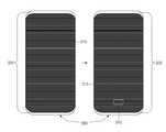
도 3은 일 실시 예에 따른 전자 장치의 전면도를 나타낸다.3 shows a front view of an electronic device according to one embodiment.
도 3을 참조하면, 일 실시 예에 따른 전자 장치(300)는 디스플레이(310) 및 하우징(320)을 포함할 수 있다. 상기 디스플레이(310)는 실질적으로 전자 장치(300)의 전면 전체를 점유할 수 있다. 상기 전자 장치(300)의 전면에는, 측면을 구성하는 하우징(320)의 일부가 노출될 수 있다.Referring to FIG. 3, an
일 실시 예에 따르면, 상기 전자 장치는, 지정된 이벤트(예: 터치, 물리 버튼의 누름, 자이로 센서/가속도 센서에서 움직임 감지 등)에 응답하여, 또는 상시에(always-on), 홈 버튼을 나타내는 가이드 이미지(315)가 디스플레이(310)의 하단에 표시될 수 있다. 예를 들면, 상기 가이드 이미지(315)에 해당하는 영역에 대응되는 내부에는 본 발명의 다양한 실시 예에 따른 모듈(예: 생체 센서, 압력 센서 등)이 배치될 수 있다.According to one embodiment, the electronic device is capable of displaying a home button in response to a specified event (e.g., touch, push of a physical button, motion detection in a gyro sensor / acceleration sensor, etc.) A
도 4는 일 실시 예에 따른 전자 장치의 분해 사시도를 나타낸다.4 shows an exploded perspective view of an electronic device according to one embodiment.
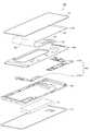
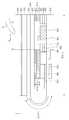
도 4를 참조하면, 일 실시 예에 따른 전자 장치(401)는 커버 글래스(410), 디스플레이 장치(420), 브래킷(430), 회로기판(440), 후면 하우징(rear housing)(450), 배터리(460), 및/또는 후면 커버(back cover)(470)를 포함할 수 있다. 다양한 실시 예에 따르면, 전자 장치(401)는 도 4에 도시된 일부 구성을 포함하지 않을 수도 있고, 도 4에 도시되지 않은 구성을 추가로 포함할 수도 있다.4, an
커버 글래스(410)는 디스플레이 장치(420)에 의해 생성된 빛을 투과시킬 수 있다. 또한, 상기 커버 글래스(410) 상에서 사용자는 신체의 일부(예: 손가락)를 접촉하여 터치(전자 펜을 이용한 접촉을 포함함)을 수행할 수 있다. 상기 커버 글래스(410)는, 예컨대, 강화 유리, 강화 플라스틱, 구부러질 수 있는(flexible) 고분자 소재 등으로 형성되어, 디스플레이 장치(420) 및 상기 전자 장치(401)에 포함된 각 구성을 외부 충격으로부터 보호할 수 있다. 다양한 실시 예에 따르면, 상기 커버 글래스(410)는 글래스 윈도우(glass window)로도 참조될 수 있다.The
디스플레이 장치(420)는 상기 커버 글래스(410) 밑에 배치 또는 결합되어, 상기 커버 글래스(410)의 적어도 일부를 통해 노출될 수 있다. 상기 디스플레이)(420)는 콘텐트(예: 텍스트, 이미지, 비디오, 아이콘, 위젯, 또는 심볼 등)를 출력하거나, 사용자로부터 터치 입력(터치, 제스처, 호버링(hovering) 포함)을 수신할 수 있다.A
일 실시 예에 따르면, 상기 디스플레이 장치(420)는 표시 영역(421) 및 상기 표시 영역(421)의 일 측(예: 상측(upper side), 하측(lower side), 좌측(left side), 우측(right side)으로부터 확장되는 연결 영역(422)을 포함할 수 있다. 상기 표시 영역(421)에는 다양한 정보를 표시하기 위한 화소들(pixels)(예: OLED 등)이 배치될 수 있다. 상기 연결 영역(422)은 상기 디스플레이 장치(420)의 배면에 배치된 FPCB(425)와 다양한 도전 패턴(배선)을 통해 전기적으로 연결될 수 있다.According to one embodiment, the
상기 연결 영역(422)의 일부는, FPCB(425)의 배면이 표시 영역(421)의 배면과 이격되어 대향하도록, 상기 표시 영역(421)의 배면을 향하여 접힐 수 있다. 다양한 실시 예에 따르면, 상기 FPCB(425)의 일부 영역(427) 상에 형성된 도전 패턴(배선)은 브래킷(430)의 측면을 지나, 지정된 커넥터를 통하여 회로 기판(440) (예: 메인 회로 기판(440m))과 전기적으로 연결될 수 있다. 다양한 실시 예에 따르면, 연결 영역(422)에는, 전자 장치(401)의 설계에 의존하여, 표시 영역(421)과 유사하게, 다양한 정보를 표시하기 위한 화소들이 배치될 수도 있다.A part of the
일 실시 예에 따르면, 상기 디스플레이 장치(420)의 디스플레이 패널은 액정 디스플레이(LCD) 패널, 발광 다이오드(LED) 디스플레이 패널, 유기 발광 다이오드(OLED) 디스플레이 패널, 또는 마이크로 전자기계 시스템(MEMS) 디스플레이 패널, 또는 전자 종이 디스플레이 패널을 포함할 수 있다. 또한 예를 들어, 상기 디스플레이 장치(420)에 포함되는 터치 패널은 정전식 터치 패널, 감압식 터치 패널, 저항식 터치 패널, 적외선 방식 터치 패널, 또는 초음파 방식 터치 패널을 포함할 수 있다. 상기 터치 패널은 디스플레이 패널 사이에 삽입되거나(애드 온(add-on) 터치 패널), 디스플레이 패널 위에 직접 형성되거나(온-셀(on-cell) 터치 패널), 또는 디스플레이 패널 내부에 포함될 수 있다(인-셀(in-cell) 터치 패널).According to one embodiment, the display panel of the
브래킷(bracket)(430)은 예를 들어, 마그네슘 합금으로 구성되어, 디스플레이 장치(420)의 아래, 및 회로기판(440) 위에 배치될 수 있다. 상기 브래킷(430)은 상기 디스플레이 장치(420) 및 상기 회로기판(440)과 결합되어 이들을 물리적으로 지지할 수 있다. 일 실시 예에 따르면, 상기 브래킷(430)에는 경년 변화에 따른 배터리(460)의 부풀어오름을 감안한 스웰링 갭(swelling gap)이 형성될 수 있다.The
회로기판(440)은 예를 들어, 메인(main) 회로기판(440m), 또는 서브(sub) 회로기판(440s)을 포함할 수 있다. 일 실시 예에 따르면, 상기 메인 회로기판(440m)과 상기 서브 회로기판(440s)은 브래킷(430) 밑에(below) 배치되고(disposed), 이들은 지정된 커넥터 또는 지정된 배선을 통해 서로 전기적으로 연결될 수 있다. 상기 회로기판들(440m, 440s)은, 예를 들어, 경성 인쇄 회로기판(rigid PCB; rigid printed circuit board)으로 구현될 수 있다. 일 실시 예에 따르면, 회로기판들(440m, 440s)에는 전자 장치(401)의 각종 전자 부품, 소자, 인쇄회로 등(예: 프로세서, 메모리, 통신 회로 등)이 배치(mount) 또는 배치(arrange)될 수 있다. 다양한 실시 예에 따르면, 회로기판(440m, 450s)은 메인보드, PBA(printed board assembly)또는, 단순히 PCB로 참조될 수 있다.The
후면 하우징(450)은 회로기판(440) 밑에 배치되어, 상기 전자 장치(401)의 각 구성을 수납할 수 있다. 후면 하우징(450)은 전자 장치(401)의 측면 외관을 형성할 수 있다. 상기 하우징(450)은 후면 케이스(rear case), 또는 리어 플레이트(rear plate) 등으로도 참조될 수 있다. 상기 후면 하우징(450)은 전자 장치(401)의 외부에 노출되지 않는 영역 및 전자 장치(401)의 외부 측면에 노출되는 영역을 포함할 수 있다. 예를 들면, 상기 전자 장치(401)의 외부에 노출되지 않는 영역은 플라스틱 사출물로 구성될 수 있다. 전자 장치(401)의 외부 측면에 노출되는 영역은, 금속으로 구성될 수 있다. 금속 소재로 이루어진 상기 측면 노출 영역은 금속 베젤(metal bezel)로도 참조될 수도 있다. 일 실시 예에 따르면, 상기 금속 베젤 중 적어도 일부는, 지정된 주파수의 신호를 송수신하기 위한 안테나 방사체로 활용될 수 있다.The
배터리(460)는 화학 에너지와 전기 에너지를 양 방향으로 변환할 수 있다. 예를 들어, 배터리(460)는 화학 에너지를 전기 에너지로 변환하여, 상기 전기 에너지를 디스플레이 장치(420) 및 회로기판(440)에 탑재된 다양한 구성 또는 모듈에 공급할 수 있다. 또는, 상기 배터리(460)는 외부로부터 공급받은 전기 에너지를 화학 에너지로 변환하여 저장할 수도 있다. 일 실시 예에 따르면, 회로기판(440)에는 배터리(460)의 충방전을 관리하기 위한 전력 관리 모듈이 포함될 수 있다.The
후면 커버(470)는 전자 장치(401)의 후면에 결합될 수 있다. 상기 후면 커버(470)는, 강화유리, 플라스틱 사출물, 및/또는 금속 등으로 형성될 수 있다. 다양한 실시예에 따르면, 후면 커버(470)는 상기 후면 하우징(450)과 일체로 구현되거나, 또는 사용자에 의해 착탈 가능(detachable)하도록 구현될 수도 있다.The
도 5a 및 도 5b는 일 실시 예에 따른 디스플레이 장치를 나타낸다.5A and 5B show a display device according to an embodiment.
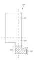
도 5a를 참조하면, 디스플레이 장치(520)는 표시 영역(521), 연결 영역(522), 및 FPCB(525)를 포함할 수 있다. 상기 디스플레이 장치(520)는 "디스플레이 모듈", 또는 "디스플레이 조립체(assembly)"로 상호교환적으로(interchangeably) 참조될 수 있다. 상기 디스플레이 장치(520)는 일 예를 들면, 도 4에 도시된 디스플레이 장치(420)에 대응할 수 있다.Referring to FIG. 5A, the
일 실시 예에 따르면, 상기 표시 영역(521)에서는 다양한 콘텐트(예: 이미지, 텍스트 등)가 출력 (또는 표시)되거나, 또는 사용자로부터의 (터치) 입력이 수신될 수 있다. 상기 연결 영역(522)은, 상기 표시 영역(521)의 일 측으로부터 확장되되, 지정된 방향으로 접히거나(fold) 휘어질(bend) 수 있다. 상기 FPCB(525)는 연결 영역(522) 상에 형성된 도전 패턴(배선)과 전기적으로 연결될 수 있다. 다양한 실시 예에 따르면, 상기 FPCB(525)의 일부 영역(527)에 형성된 도전 패턴(배선)은 지정된 커넥터를 통해 메인 회로 기판과 전기적으로 연결될 수 있다.According to one embodiment, various contents (e.g., images, text, etc.) may be output (or displayed) in the
도 5b를 참조하면, 도 5a에 도시된 보조선 x-x'에 대응하는 디스플레이(520)의 단면도가 도시되어 있다.Referring to FIG. 5B, a cross-sectional view of the
일 실시 예에 따르면, 디스플레이(520)의 표시 영역(521)에는 터치스크린 디스플레이 패널(521-1), 합성수지 필름(예: 폴리이미드(PI: polyimide) 필름)(521-2), 기타 패널/필름 층(예: 보호 필름(PF: protection film), 백 패널 등)(521-3)이 적층될 수 있다. 상기 합성수지 필름(521-2)의 제1 방향으로 향한 앞면(a front surface facing a first direction)에는 디스플레이 패널(521-1)이 배치될 수 있고, 상기 합성수지 필름(521-2)의 제2 방향으로 향한 배면(a rear surface facing a second direction)에는 기타 패널/필름 층(521-3)이 배치될 수 있다.According to one embodiment, the
일 실시 예에 따르면, 디스플레이(520)의 연결 영역(522)에는 표시 영역(521)에 포함된 다양한 층의 전부 또는 일부 층이 적층될 수 있다. 예를 들어, 상기 연결 영역(522)은 상기 표시 영역(521)의 일 측으로부터 확장된 합성수지 필름(521-2)으로 구성될 수 있다. 상기 합성수지 필름(521-2)의 제1 방향 앞면에는 하드웨어 모듈(531)(예: 디스플레이 구동 회로(DDI: display driver integrated circuit) 등)이 배치될 수 있다.According to one embodiment, all or some of the various layers included in the
일 실시 예에 따르면, FPCB(525)는 제1 방향 앞면 및/또는 제2 방향 배면에 다양한 도전 패턴(배선)을 포함할 수 있다. FPCB(525)의 앞면 및 배면 상에 형성된 도전 패턴(배선)은 상기 연결 영역(522) 상에 형성된 도전 패턴(배선)과 전기적으로 연결될 수 있다. 일 실시 예에 따르면, FPCB(525)의 제2 방향 배면 상에는 지정된 기능을 수행하는 모듈(예: 생체 센서. 또는 압력 센서)(532)이 배치될 수 있다.According to one embodiment, the
일 실시 예에 따르면, 상기 연결 영역(522)의 일부는, FPCB(525)의 제2 방향 배면이 표시 영역(521)의 배면과 이격되어 대향하도록, 상기 표시 영역(521)의 배면을 향하여 접힐 수 있다. 이에 따라서, 상기 FPCB(525)의 배면 상에 배치된 모듈(532)은, 표시 영역(521)의 밑에(below) 배치될 수 있다.A part of the
도 6a는 일 실시 예에 따른, 전자 장치의 하드웨어 모듈의 배치 구조를 나타낸다.6A illustrates an arrangement of hardware modules of an electronic device, according to one embodiment.
도 6a를 참조하면, 전자 장치는 디스플레이(610), FPCB(620), 백 패널(back panel)(630), 제1 (하드웨어) 모듈(640), 완충 부재(645), 접착층(653), 압력 센서(655), 제2 (하드웨어) 모듈(650), 및 제3 (하드웨어) 모듈(660)을 포함할 수 있다. 일 실시 예에 따르면, 상기 디스플레이(610) 및 FPCB(620)는 디스플레이 장치(601)를 구성할 수 있다. 다양한 실시 예에 따르면, 상기 전자 장치는 도 6a에 도시된 일부 구성을 포함하지 않을 수도 있고, 도 6a에 도시되지 않은 구성을 추가로 포함할 수도 있다.6A, the electronic device includes a
디스플레이(610)는 표시 영역(611) 및 상기 표시 영역(611)의 일 측으로부터 연장(extend)되는 연결 영역(612)을 포함할 수 있다. 상기 연결 영역(612)의 일부 영역(휘어진 영역)(612-1)는, FPCB(620)의 배면이 표시 영역(611)의 배면과 이격되어 대향하도록, 상기 표시 영역(611)의 배면을 향하여 접힐 수 있다.The
일 실시 예에 따르면, 상기 디스플레이(610)의 표시 영역(611)은 복수의 층을 포함할 수 있다. 예를 들면, 상기 복수의 층은 접착층(adhesive layer), 편광층(polarization layer), 디스플레이 패널, 및 합성수지 필름(예: PI 필름) 중 적어도 하나를 포함할 수 있다. 상기 표시 영역(611)에서는 상기 디스플레이 패널에 포함된 다수의 화소들(pixels)에 의하여 다양한 콘텐츠가 출력될 수 있다.According to one embodiment, the
일 실시 예에 따르면, 상기 디스플레이(610)의 연결 영역(612)은 FPCB(620) 상의 지정된 모듈(예: 제1 모듈(640))이 디스플레이(610)와 이격되어 대향하도록 휘어질 수 있다. 상기 연결 영역(612)이 휘어짐에 따라서 상기 연결 영역(612)의 적어도 일부분은 지정된 곡률(curvature)을 형성할 수 있다.According to one embodiment, the
상기 연결 영역(612)은 상기 표시 영역(611)에 포함된 복수의 층 중 적어도 하나의 층을 포함할 수 있다. 일 실시 예에 따르면, 상기 연결 영역(612)은 합성수지 필름을 적어도 포함할 수 있다. 일 예를 들어, 상기 연결 영역(612)은 디스플레이 패널(또는, 다수의 화소들)이 형성되지 않은 PI 재질로 형성될 수 있다. 또 다른 예에 따르면, 상기 연결 영역(612)에는 다수의 화소들을 포함한 디스플레이 패널의 적어도 일부가 형성될 수도 있다.The
다양한 실시 예에 따르면, 상기 연결 영역(612)의 휘어진 영역(612-1)은 휘어진 부분의 깨짐을 방지하기 위한 BPL(bending protect layer)를 더 포함할 수 있다. 또한, 상기 연결 영역(612)의 평탄 영역(612-2)의 일 면(앞면 또는 배면) 상에는 제3 모듈(660)(예: 디스플레이(610))이 배치될 수 있다.According to various embodiments, the bent region 612-1 of the
FPCB(620)는 디스플레이(610)의 연결 영역(612)과 전기적으로 연결될 수 있다. 예를 들어, 상기 FPCB(620)의 배면(제1 면; 디스플레이(610)의 표시 영역(611)과 마주보는 면)에는 제1 모듈(640)(예: 생체 센서, 압력 센서 등)이 배치될 수 있다. 또한, 예를 들면, 상기 FPCB(620)의 앞면(제2 면; 상기 제1 면의 반대 방향 표면)에는 또 다른(another) 지정된 모듈, 즉, 제2 모듈(650)이 배치될 수 있다. 상기 또 다른 지정된 모듈(예: 생체 센서 IC, 압력 센서 IC 등)은 상기 지정된 모듈의 기능과 연관되어 수행되도록 설정될 수 있다.The
백 패널(630)은 디스플레이(610)의 표시 영역(611) 밑에, 예컨대, 상기 디스플레이(610)의 배면에 형성 (혹은 배치)될 수 있다. 예를 들면, 상기 백 패널(630)은, 디스플레이(610)에서 발생한 빛을 차단하기 위한 차광층(이른바, EMBO 층), 디스플레이(610) 상에서의 사용자 입력에 의한 충격을 완화하기 위한 완충층(예: 스폰지 층), 및 방열을 위한 금속판층(예: 구리(Cu) 그래파이트(graphite) 층), 전자 펜 센서층 중 적어도 하나를 포함할 수 있다. 일 실시 예에 따르면, 상기 백 패널(630) 중 제1 모듈(640)에 대응하는 영역, 즉, 상기 제1 모듈(640)의 상방(above)에는 개구(opening)가 형성될 수 있다.The
제1 모듈(640)은 디스플레이(610) 밑에 배치될 수 있는 다양한 단수 또는 복수의 하드웨어 모듈을 포함할 수 있다. 예를 들면, 상기 제1 모듈(640)은 생체 센서(예: 지문 센서), 압력 센서, 또는 양자 모두를 포함할 수 있다. 예컨대, 상기 제1 모듈(640)이 생체 센서 및 압력 센서를 포함하는 경우, 상기 압력 센서는 상기 생체 센서에 인접하여(adjacent to) FPCB(620)의 배면(제1 면) 상에 적어도 하나 배치될 수 있다(도 9 및 도 10 참조). 이 경우, 예를 들어, 압력 센서가 지정된 값 이상의 압력을 검출하면, 생체 센서가 활성화될 수 있다(도 12 및 도 13 참조).The
완충 부재(645)는 상기 제1 모듈(640)의 표면 중, 상기 제1 모듈(640)이 디스플레이(610)에 대향하는(facing) 면에 배치될 수 있다. 상기 완충 부재(645)는 사용자로부터의 물리적인 (터치) 입력에 의해 디스플레이(610)가 휘어져 제1 모듈(640)을 압박하는 것을 방지할 수 있다. 예를 들면, 상기 완충 부재(645)는 우레탄 폼(예: 포론(Poron))으로 구성될 수 있다.The buffering
접착층(653)은 공기를 통과시키고 수분을 차단하는 방수 부재로 이루어질 수 있다. 일 실시 예에 따르면, 백 패널(630) 중 개구를 둘러싼 영역은 접착층(653)을 통하여 FPCB(620)와 부착될 수 있다. 이에 따라서, 제1 모듈(640)은 디스플레이(610), 백 패널(630)에 형성된 개구의 내측면, 접착층(653), 및 FPCB(620)에 의해 밀폐될 수 있다.The
압력 센서(655)는 접착층(653)을 통하여 백 패널(630)과 FPCB(620) 사이에 배치될 수 있다. 따라서, 상기 압력 센서(655)는, 디스플레이(610) 상에서 사용자로부터의 물리적인 (터치) 입력이 수신된 경우, 해당 물리적인 (터치) 입력의 압력을 검출할 수 있다.The
도 6b는 일 실시 예에 따른, 전자 장치의 하드웨어 모듈의 배치 구조를 나타낸다.6B illustrates an arrangement of hardware modules of an electronic device, according to one embodiment.
도 6b를 참조하면, 전자 장치는 디스플레이(610), FPCB(620), 백 패널(630), 접착층(653), 압력 센서(655), 제2 (하드웨어) 모듈(650), 및 제3 (하드웨어) 모듈(660)을 포함할 수 있다. 일 실시 예에 따르면, 상기 디스플레이(610) 및 FPCB(620)는 디스플레이 장치(601)를 구성할 수 있다. 도 6b의 설명에 있어서, 도 6a에서와 동일한 참조 부호가 부착된 동일한 구성에 대한 설명은 생략될 수 있다.6B, the electronic device includes a
도 6b에 도시된 일 실시 예에 따른 백 패널(630)에는, 도 6a에 도시된 백 패널(630)과 달리, 개구가 형성되지 않을 수 있다. 또한, 도 6b에 도시된 전자 장치에서 백 패널(630) 밑에는 도 6a의 제1 모듈(640)와 같은 구성이 생략될 수 있다. 일 실시 예에 따르면, 상기 백 패널(630) 밑에는 접착층들(653) 및 압력 센서(655)가 배치될 수 있다.In the
일 실시 예에 따르면, 압력 센서(655)는 접착층(653)들을 통하여 백 패널(630)과 FPCB(620) 사이에 배치될 수 있다. 상기 압력 센서(655)는 디스플레이(610) 상에서 사용자로부터의 물리적인 (터치) 입력이 수신된 경우, 상기 물리적인 (터치) 입력의 압력을 검출할 수 있다.According to one embodiment, the
상기 압력 센서(655)가 지정된 값 이상의 압력을 검출하면 전자 장치는 지정된 기능(전자 장치에 포함된 구성요소들의 기능, 동작의 제어)을 수행할 수 있다.When the
예를 들어, 전자 장치가 슬립 모드(디스플레이(610)를 오프하고, 저전력 상태에서 사용자의 입력을 대기하는 모드)로 동작하는 중에, 압력 센서(655)에서 지정된 값 이상의 압력이 검출되면, 상기 전자 장치는 상기 디스플레이(610)를 활성화 시키고 홈 화면(home screen) 또는 잠금 화면(lock screen)을 상기 디스플레이(610)에 출력할 수 있다. 다양한 실시 예에 따르면, 상기 전자 장치는 상기 압력 센서(655)에서 검출된 압력의 세기에 따른 UI(user interface)를 상기 디스플레이(610)에 출력할 수도 있다.For example, if a pressure greater than a specified value is detected in the
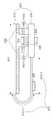
도 7a 및 도 7b는 또 다른 실시 예에 따른 하드웨어 모듈의 배치 구조를 나타낸다.7A and 7B show a layout structure of a hardware module according to another embodiment.
도 7a를 참조하면, 전자 장치는 커버 글래스(710), OCA(optical clear adhesive) 층(715), 편광층(720), 디스플레이 패널(730), PI 필름(735), 보호 필름(737), BPL(739), 백 패널(740), 지문 센서(생체 센서의 일례)(750), 완충 부재(755), 접착층(761, 765), 압력 센서(763), FPCB(770), 접착층(780), 보호 필름(785), 디스플레이 구동 회로(790)를 포함할 수 있다. 일 실시 예에 따르면, OCA층(715), 편광층(720), 디스플레이 패널(730), PI 필름(735), BPL(739), 및 FPCB(770)는 디스플레이 장치를 구성하는 것으로 이해될 수 있다. 또한, 도 7a에서는 생체 센서로서 지문 센서(750)를 예로 들고 있으나, 이에 제한되지 않는다. 예컨대, 상기 지문 센서(750)는 홍채 센서로 대체될 수도 있다.7A, the electronic device includes a
커버 글래스(710)는 디스플레이(730)에 의해 생성된 빛을 투과시킬 수 있다. 또한, 상기 커버 글래스(710) 상에서 사용자는 신체의 일부(예: 손가락)(7)를 접촉하여 터치을 수행할 수 있다.The
OCA 층(715)는 투명한 접착층으로서, 커버 글래스(710)와 편광층(720)을 접착할 수 있다.The
편광층(또는, 편광 필름)(720)은 실외같이 밝은 곳에서의 패널 시인성 개선을 위해 외광(外光)의 반사를 방지할 수 있다. 상기 편광층(720)은 PET(poly ethylene terephthalate) 필름 또는 TAC(tri-acetyl cellulose) 필름으로 구성될 수 있다.The polarizing layer (or polarizing film) 720 can prevent reflection of external light for improving the panel visibility in a bright place such as outdoors. The
디스플레이 패널(730)은, 예를 들어, 스캔 라인(scan line) 및 데이터 라인(data line), 상기 스캔 라인 및 상기 데이터 라인으로부터 공급되는 신호들에 기반하여 빛을 생성하는 발광 소자(예: OLED), 상기 발광 소자가 배치되는 기판(예: 저온 폴리실리콘(LTPS: low temperature poly silicon) 기판), 상기 발광 소자를 보호하기 위한 박막 봉지 필름(TFE: thin film encapsulation)을 포함할 수 있다.The
PI 필름(735)(플렉서블 부재의 일례)은 디스플레이 패널(730)의 밑에 배치될 수 있다. 상기 PI 필름(735)은 디스플레이 패널(730)에 전력 및/또는 신호를 공급하기 위한 배선을 포함할 수 있다. 상기 PI 필름(735)은 디스플레이 패널(730)에 접촉되는 제1 영역과, 디스플레이 패널(730)과 접촉하지 않는 제2 영역을 포함할 수 있다.The PI film 735 (an example of the flexible member) may be disposed under the
일 실시 예에 따르면, 상기 PI 필름(735)의 상기 제2 영역은 디스플레이 패널(730)의 배면을 향하여 접힐 수 있다. 상기 제2 영역은 휘어진 영역(735-1) 및 평탄 영역(735-2)으로 구분될 수 있다. 상기 휘어진 영역(735-1)으로 인해, 상기 PI 필름(735)의 평탄 영역(735-2)은 디스플레이 패널(730)과 대향할 수 있고, 지문 센서(750)는 디스플레이 패널(730)과 이격되어 대향하도록 배치될 수 있다.According to one embodiment, the second region of the
다양한 실시 예에 따르면, 상기 PI 필름(735)은 디스플레이 패널(730)의 상방에 배치되거나, 또는 디스플레이 패널(730)의 일부 구성으로 상기 디스플레이 패널(730)에 포함될 수도 있다.According to various embodiments, the
보호 필름(737)은 PI 필름(735)의 밑에 배치되어, 상기 PI 필름(735)을 지지할 수 있다.A
BPL(739)은 PI 필름(735)의 휘어진(bent) 영역(735-1) 및/또는 평탄 영역(735-2)의 적어도 일부에 부착될 수 있다. 상기 BPL(739)은 상기 휘어진 영역(735-1)에서의 깨짐을 방지할 수 있다.The
백 패널(740)은 보호 필름(737) 밑에, 예컨대, 상기 디스플레이(610)의 배면에 형성 (혹은 배치)될 수 있다. 예를 들면, 상기 백 패널(740)은, 차광층(예: EMBO 층)(741), 완충층(예: 스폰지 층)(743), 및 금속판층(예: 구리(Cu) 그래파이트(graphite) 층)(745) 중 적어도 하나를 포함할 수 있다.The
일 실시 예에 따르면, 상기 백 패널(740) 중 생체 센서(750)에 대응하는 영역, 즉, 상기 지문 센서(750)의 상방(above)에는 개구(Wopening)가 형성될 수 있다. 상기 개구(Wopening)로 인해 사용자의 손가락(7)에 형성된 지문은 지문 센서(750)에 의해 인식될 수 있다. 예를 들면, 디스플레이 패널(730)에 의해 생성된 빛은 상기 손가락(7)의 지문에서 반사되고, 상기 반사된 빛은 커버 글래스(710), OCA 층(715), 편광층(720), 디스플레이 패널(730), PI 필름(735), 및 보호 필름(737), 및 상기 개구(Wopening)를 통해 지문 센서(750)에 도달될 수 있다. 즉, 상기 지문 센서(750)는 디스플레이 패널(730)에 포함된 복수개의 픽셀들 중 적어도 하나의 픽셀을 광원으로 이용하도록 설정될 수 있다.According to one embodiment, an opening (Wopening ) may be formed in an area corresponding to the
지문 센서(750)에서는 손가락의 지문 이미지가 획득(capture)될 수 있다. 일 실시 예에 따르면, 상기 지문 센서(750)는 광학식 지문 센서에 해당할 수 있다. 상기 지문 센서(750)는 내장된 이미지 센서(예: CMOS, CCD)를 이용하여 지문 이미지를 획득(capture)할 수 있다. 상기 지문 센서(750)에서는, 예를 들어, 상기 지문 이미지로부터 지문의 유니크(unique)한 지문 특징점(fingerprint minutiae)이 추출될 수 있다. 상기 지문 특징점은, 예를 들어, 지문에 포함된 융선의 끝점(ridge ending), 크로스오버(crossover), 분기점(bifurcation), 구멍(pore) 등 다양한 특징점을 포함할 수 있다. 상기 지문 특징점은 기 등록된 지문 특징점과 대조됨으로써 사용자 인증에 이용될 수 있다.In the
완충 부재(755)는 지문 센서(750)의 표면에 배치될 수 있다. 상기 완충 부재(755)는 사용자의 손가락(7)으로부터의 물리적인 (터치) 입력에 의해 보호 필름(737)이 지문 센서(750)을 압박하는 것을 방지할 수 있다. 예를 들면, 상기 완충 부재(755)는 우레탄 폼(예: 포론(Poron))으로 구성될 수 있다.The
접착층(761, 765)은 공기를 통과시키고 수분을 차단하는 부재로 이루어질 수 있다. 일 실시 예에 따르면, 접착층(761) 및 접착층(765) 사이에는 압력 센서(763)가 배치될 수 있다. 상기 압력 센서(763)는, 커버 글래스(710), OCA 층(715), 편광층(720), 디스플레이 패널(730), PI 필름(735), 보호 필름(737), 백 패널(740), 및 접착층(761)을 통해 전달되는 사용자의 손가락(7)에 의한 압력을 감지할 수 있다.The
일 실시 예에 따르면, 백 패널(740) 중 개구를 둘러싼 영역은, 접착층(761), 압력 센서(763), 및 접착층(765)을 통하여 FPCB(770)와 부착될 수 있다. 이에 따라서, 지문 센서(750)는 보호 필름(737), 백 패널(740)에 형성된 개구의 내측면, 접착층(761), 압력 센서(763), 접착층(765), 및 FPCB(770)에 의해 밀폐될 수 있다.An area of the
FPCB(770)는 PI 필름(735)의 평탄 영역(735-2)과 전기적으로 연결될 수 있다. 예컨대, FPCB(770)는 PI 필름(735)에 형성된 도전 패턴(또는 배선)과 전기적으로 연결될 수 있다. 일 실시 예에 따르면, FPCB(770)의 일 면에는 지문 센서(750)가 배치될 수 있다. 도시하지는 않았으나, 다양한 실시 예에 따르면, FPCB(770)의 또 다른 일 면에는 상기 지문 센서(750)의 드라이버 IC가 배치될 수 있다.The
접착층(780) 및 보호 필름(785)은 백 패널(740) 및 PI 필름(735) 사이에 부착되어, 커버 글래스(710), OCA 층(715), 편광층(720), 디스플레이 패널(730), PI 필름(735), 및 보호 필름(737)을 물리적으로 지지할 수 있다.The
디스플레이 구동 회로(790)는 디스플레이 패널(730)을 제어할 수 있다. 상기 디스플레이 구동 회로(790)는 프로세서(호스트)로부터 수신한 영상 데이터에 대응하는 영상 신호를 미리 설정된 프레임수로 디스플레이 패널(730)에 공급할 수 있다. 상기 디스플레이 구동 회로(790)는 PI 필름(735)의 평탄 영역(735-2)의 일 면에 배치될 수 있다.The
도 7b를 참조하면, 또 다른 실시 예에 따른 하드웨어 모듈의 배치 구조가 도시되어 있다. 도 7b에 도시된 전자 장치는 도 7a에 도시된 전자 장치의 구성과 동일 또는 유사한 구성을 포함할 수 있다. 도 7b에 대한 설명에 있어서, 도 7a와 동일한 참조 부호가 부착된 동일한 구성에 대한 설명은 생략될 수 있다.Referring to FIG. 7B, a layout structure of a hardware module according to another embodiment is shown. The electronic device shown in Fig. 7B may have the same or similar configuration as that of the electronic device shown in Fig. 7A. In the description of FIG. 7B, description of the same configuration with the same reference numerals as in FIG. 7A can be omitted.
일 실시 예에 따르면, 백 패널(740)은, 차광층(741), 완충층(743), 금속판층(745)에 더하여 전자 펜 센서층(744)을 더 포함할 수 있다. 상기 전자 펜 센서층(744)은 전자 펜(예: 위치 지시기(position indicator), 스타일러스(stylus), 디지타이저용 펜 등)에 의한 접촉 여부 및 접촉 위치를 감지하는데 이용될 수 있다. 전자 펜 센서 층(744)은 전자 펜 센서 시트, 디지타이저층 등으로 다양하게 참조될 수 있다.According to one embodiment, the
도 7b에는, 전자 펜 센서 층(744)은 완충층(743) 및 금속판층(745) 사이에 배치된 것으로 도시되어 있으나, 이에 제한되지 않는다. 예컨대, 상기 전자 펜 센서 층(744)은 차광층(741)과 완충층(743) 사이에 배치될 수 있고, 차광층(741)과 보호 필름(737) 사이에 배치될 수도 있다.7B, the electronic
도 8a 및 도 8b는 또 다른 실시 예에 따른 하드웨어 모듈의 배치 구조를 나타낸다.8A and 8B show a layout structure of a hardware module according to another embodiment.
도 8a를 참조하면, 전자 장치는 커버 글래스(810), OCA 층(815), 편광층(820), 디스플레이 패널(830), PI 필름(835), 보호 필름(837), 백 패널(840), 지문 센서(850), 완충 부재(855), 접착층(861, 765), 압력 센서(863), FPCB(870), 접착층(880), 보호 필름(885), 디스플레이 구동 회로(890)을 포함할 수 있다. 일 실시 예에 따르면, OCA층(815), 편광층(820), 디스플레이 패널(830), PI 필름(835), 및 FPCB(870)는 디스플레이 장치를 구성하는 것으로 이해될 수 있다. 또한, 도 8a에서는 생체 센서로서 지문 센서(850)를 예로 들고 있으나, 이에 제한되지 않는다. 예컨대, 상기 지문 센서(850)는 홍채 센서로 대체될 수도 있다. 도 8a의 설명에 있어서, 도 7a에 도시된 구성과 동일한 구성에 관한 설명은 생략될 수 있다.8A, the electronic device includes a
일 실시 예에 따르면, FPCB(870)는 디스플레이 패널(830)과 전기적으로 연결될 수 있다. 예를 들면, 상기 FPCB(870)는 핫바(hot bar) 또는 납땜(soldering)을 통해 상기 디스플레이 패널(830)과 전기적으로 연결될 수 있다.According to one embodiment, the
일 실시 예에 따르면, FPCB(870)는 휘어진 영역(bent area)(870-1), 및 상기 휘어진 영역(870-1)과 이어진 평탄 영역(870-2)을 포함할 수 있다. 상기 휘어진 영역(870-1)은 상기 디스플레이 패널(830)과 연결되되 상기 디스플레이 패널(830)의 배면을 향해 접힐 수 있다. 도 7a의 경우와 달리 도 8a에서는 FPCB(870)가 접힐 수 있다.According to one embodiment, the
상기 FPCB(870)의 휘어진 영역(870-1)으로 인해 FPCB(870)의 평탄 영역(870-2)의 배면은 상기 디스플레이 패널(830)의 배면과 이격되어 대향할 수 있다. 이에 따라, 센서들(850 863)과 디스플레이 패널(830)은 서로 이격되어 대향할 수 있다.The back surface of the flat area 870-2 of the
일 실시 예에 따르면, 상기 FPCB(870)의 평탄 영역(870-2)의 배면(제1 면; 디스플레이 패널(830)과 대향하는 면) 위에는 지문 센서(850), 및 상기 지문 센서(850)에 인접하여 적어도 하나의 압력 센서(863)가 배치될 수 있다. 상기 압력 센서(863)는 접착층(865)을 통하여 상기 FPCB(870)의 평탄 영역(870-2)의 배면과 부착될 수 있다. 한편, 디스플레이 구동 회로(890)는 FPCB(870)의 평탄 영역(870-2)의 앞면(제2 면; 보호 필름(885)이 부착된 면의 반대면)에 배치될 수 있다.The
도 8b를 참조하면, 또 다른 실시 예에 따른 하드웨어 모듈의 배치 구조가 도시되어 있다. 도 8b에 도시된 전자 장치는 도 8a에 도시된 전자 장치의 구성과 동일 또는 유사한 구성을 포함할 수 있다. 도 8b에 대한 설명에 있어서, 도 8a와 동일한 참조 부호가 부착된 동일한 구성에 대한 설명은 생략될 수 있다.Referring to FIG. 8B, a layout structure of a hardware module according to another embodiment is shown. The electronic device shown in Fig. 8B may include the same or similar configuration as that of the electronic device shown in Fig. 8A. In the description of FIG. 8B, the description of the same configuration with the same reference numerals as in FIG. 8A can be omitted.
일 실시 예에 따르면, 백 패널(840)은, 차광층(841), 완충층(843), 금속판층(845)에 더하여 전자 펜 센서층(844)를 더 포함할 수 있다. 상기 전자 펜 센서층(844)은 전자 펜에 의한 접촉 여부 및 접촉 위치를 감지하는데 이용될 수 있다. 도 8b에 있어서, 전자 펜 센서 층(844)은 완충층(843) 및 금속판층(845) 사이에 배치된 것으로 도시되어 있으나, 이에 제한되지 않는다. 예컨대, 상기 전자 펜 센서 층(844)은 차광층(841)과 완충층(843) 사이에 배치될 수 있고, 차광층(841)과 보호 필름(837) 사이에 배치될 수도 있다.The
도 9는 일 실시 예에 따른 생체 센서 및 압력 센서의 배치 구성을 나타낸다.9 shows a configuration of a biosensor and a pressure sensor according to an embodiment.
도 9를 참조하면, 압력 센서(920a)는 생체 센서(예: 지문 센서)(910a)를 둘러싸도록 배치될 수 있다. 일 실시 예에 따르면, 상기 압력 센서(920a)는 제1 전극(921a), 제2 전극(925a), 및 유전층(dielectric layer)(923a)을 포함할 수 있다. 예컨대, 상기 압력 센서(920a)는 상기 터치에 의해 변화하는 상기 제1 전극(921a) 및 상기 제2 전극(925a) 사이의 정전용량에 기초하여 상기 터치의 압력을 감지할 수 있다.Referring to Fig. 9, the
일 실시 예에 따르면, 상기 제1 전극(921a) 및/또는 제2 전극(925a)은 투명 또는 불투명하게 구현될 수 있다. 예를 들어, 불투명하게 구현되는 경우, 상기 제1 전극(921a) 및/또는 제2 전극(925a)은 구리(Cu), 은(Ag), 마그네슘(Mg), 티타늄(Ti), 불투명한 그래핀(graphene)으로 구현될 수 있다. 또한, 투명하게 구현되는 경우, 상기 제1 전극(921a) 및/또는 제2 전극(925a)은 ITO(indium tin oxide), IZO(indium zinc oxide), 은 나노 와이어(Ag nanowire), 메탈 메쉬(metal mesh), 투명 고분자 전도체, 투명 그래핀으로 구현될 수 있다.According to one embodiment, the
유전층(923a)은 복원력이 있는 유전물질, 예를 들어, 실리콘 폼(foam), 실리콘 멤브레인(membrane), 스폰지, 고무, 폴리머(예: PC(polycabonate), PET(polyethylene terephthalate) 등)으로 구현될 수 있다.The
또 다른 실시 예에 따르면, 상기 압력 센서(920b)는 생체 센서(910b)를 둘러싸도록 배치되되, 복수 개(예: 4개)의 압력 센서로 구분될 수 있다. 이 경우, 상기 압력 센서(920b)는, 압력의 세기뿐만 아니라, 해당 압력이 가해진 위치의 분포를 감지할 수도 있다.According to another embodiment, the
도 10은 다양한 실시 예에 따른 생체 센서 및 압력 센서의 배치 구성을 나타낸다.Fig. 10 shows the arrangement of a biosensor and a pressure sensor according to various embodiments.
전자 장치(1001)을 참조하면, 일 실시 예에 따른 압력 센서(1012)는 생체 센서(예: 지문 센서)(1011)를 둘러싸도록 배치될 수 있다. 생체 센서(1011)는 가로변이 세로변보다 더 긴 직사각형 형상을 가질 수 있다. 상기 압력 센서(1012)는 단일의 제1 전극, 제2 전극, 및 유전층을 포함할 수 있다(도 9 참조). 전자 장치(1002)을 참조하면, 압력 센서(1022)는 생체 센서(예: 지문 센서)(1021)를 둘러싸도록 배치될 수 있다. 이때, 생체 센서(1021)는 세로변이 가로변보다 더 긴 직사각형 형상을 가질 수 있다.Referring to the
전자 장치(1003)을 참조하면, 일 실시 예에 따른 2개의 압력 센서(1032-1, 1032-2)는 각각 생체 센서(예: 지문 센서)(1031)의 상측 가로변 및 하측 가로변에 인접하게 배치될 수 있다. 전자 장치(1004)을 참조하면, 2개의 압력 센서(1042-1, 1042-2)는 각각 생체 센서(예: 지문 센서)(1041)의 좌측 세로변 및 우측 세로변에 인접하게 배치될 수 있다.Referring to the
전자 장치(1005)을 참조하면, 일 실시 예에 따른 4개의 압력 센서(1052-1, 1052-2, 1052-3, 1052-4)는 각각 생체 센서(예: 지문 센서)(1051)의 네 변에 인접하게 배치될 수 있다. 예를 들면, 사용자의 손가락(10-5a)은 생체 센서(1051)의 우측 상단 인근에 지정된 압력으로 터치(이른바, "포스 터치")할 수 있다. 이 경우, 전자 장치(1005)는 상측에 배치된 압력 센서(1052-1) 및 우측에 배치된 압력 센서(1052-2)를 통해 상기 손가락(10-5a)에 의한 포스 터치를 인식할 수 있다. 또 다른 예를 들면, 사용자의 손가락(10-5b)은 생체 센서(예: 지문 센서)(1051)의 좌측 하단 인근에 포스 터치할 수 있다. 이 경우, 전자 장치(1005)는 하측에 배치된 압력 센서(1062-3) 및 좌측에 배치된 압력 센서(1062-4)를 통해 손가락(10-5b)에 의한 포스 터치를 인식할 수 있다. 상기 전자 장치(1005)에 따르면, 손가락(10-5a)에 의한 포스 터치 및 손가락(10-5b)에 의한 포스 터치는 상이한 입력으로 인식될 수 있다. 이에 따라서, 각각의 입력에 대응하는 기능을 제공할 수 있다.Referring to the
도 11a 및 도 11b는 다양한 실시 예에 따른 생체 센서 및 압력 센서의 FPCB 배치 구조를 나타낸다.11A and 11B show the FPCB arrangement structure of the biosensor and the pressure sensor according to various embodiments.
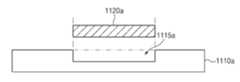
도 11a을 참조하면, 일 실시 예에 따른 생체 센서(예: 지문 센서)(1120a)는 FPCB(1110a)의 일 표면 상에 배치될 수 있다. 예를 들어, 상기 생체 센서(1120a)는 도 6a에 도시된 640, 도 7a에 도시된 750, 또는 도 8a에 도시된 850에 해당할 수 있고, 상기 FPCB(1110a)는 도 6a에 도시된 620, 도 7a에 도시된 770, 또는 도 8a에 도시된 870에 해당할 수 있다. 일 실시 예에 따르면, FPCB(1110a)의 일 표면 상에는 요부(recessed portion)(1115a)가 형성될 수 있다. 생체 센서(1120a)는 상기 요부(1115a)에 안착될 수 있다.Referring to FIG. 11A, a biosensor (e.g., a fingerprint sensor) 1120a according to an embodiment may be disposed on one surface of the
도 11b를 참조하면, 일 실시 예에 따른 생체 센서(예: 지문 센서)(1120b) 및 복수의 압력 센서(1130b)는 FPCB(1110b)의 일 표면 상에 배치될 수 있다. 예를 들어, 상기 복수의 압력 센서(1130b)는 도 6a에 도시된 655, 도 7a에 도시된 743, 또는 도 8a에 도시된 843에 대응할 수 있다. 다양한 실시 예에 따르면, 상기 복수의 압력 센서(1130b)의 앞면 및 배면에는 접착층(예: tape)이 추가로 부착될 수 있다. 일 실시 예에 따르면, FPCB(1110b)의 일 표면 상에는 요부(1115b)가 형성될 수 있다. 생체 센서(1120b) 및 복수의 압력 센서(1130b)는 FPCB(1110b)에 형성된 요부(1115b)에 안착될 수 있다.Referring to Fig. 11B, a biometric sensor (e.g., a fingerprint sensor) 1120b and a plurality of
도 11a 및 도 11b의 실시 예에 따르면, FPCB(1110a, 1110b)에 형성된 요부(1115a, 1115b)로 인해 생체 센서(1120a, 1120b)가 배치된 FPCB FPCB(1110a, 1110b)의 두께가 감소할 수 있다.11A and 11B, the thicknesses of the
도 12는 일 실시 예에 따른 지문 인증 방법의 흐름도를 나타낸다.12 shows a flowchart of a fingerprint authentication method according to an embodiment.
도 12를 참조하면, 일 실시 예에 따른 지문 인증 방법은 동작 1201내지 1213를 포함할 수 있다. 상기 동작 1201내지 1213의 각 동작은, 예를 들어, 전자 장치의 프로세서에 의해 수행(혹은, 실행)될 수 있는 인스트럭션(명령어)들로 구현될 수 있다. 상기 인스트럭션들은, 예를 들어, 컴퓨터 기록 매체 또는 전자 장치의 내장/외장 메모리에 저장될 수 있다.Referring to FIG. 12, the fingerprint authentication method according to one embodiment may include
동작 1201에서, 전자 장치는 압력 센서를 이용하여 손가락이 디스플레이(또는, 커버 글래스)의 일부(예: 도 3에 도시된, 홈 버튼을 나타내는 가이드 이미지(315)가 표시된 영역)에 가한 압력을 감지할 수 있다. 일 실시 예에 따르면, 전자 장치는 상기 디스플레이의 디스플레이 패널이 켜져(ON) 있는 상태뿐만 아니라, 꺼진(OFF) 상태에서도, 상기 손가락에 의해 가해진 압력을 감지할 수 있다.In
동작 1203에서, 전자 장치는 동작 1201에서 감지된 압력이 지정된 값 이상이면 지문 센서(생체 센서의 일례)를 활성화시킬 수 있다. 즉, 사용자로부터 포스 터치가 수신되면 지문 센서 및 이를 구동하는 지문 센서 IC가 동작하도록 트리거될 수 있다.At
동작 1205에서, 전자 장치는 활성화된 지문 센서를 이용하여 손가락의 지문(의 특징점)을 검출할 수 있다. 예를 들어, 상기 지문 센서가 광학식 지문 센서에 해당하는 경우, 지문 인식의 정확도를 높이기 위해 상기 지문 센서가 배치된 영역에 대응되는 디스플레이의 일부(예: 도 3에 도시된, 홈 버튼을 나타내는 가이드 이미지(315)가 표시된 영역)는 지정된 밝기로 빛을 방출할 수 있다.In
동작 1207에서, 전자 장치는 동작 1205에서 검출된 지문을 메모리에 저장되거나, 또는 서버에 등록된 지문과 대조할 수 있다.In
동작 1209에서, 전자 장치는 동작 1207에서 대조된 지문이 등록 지문과 매칭되었는지 판단할 수 있다. 동작 1209에서의 판단 결과 상기 검출된 지문이 상기 등록 지문과 매칭되는 경우, 동작 1211에서, 전자 장치는 지정된 제1 기능을 수행할 수 있다.In
예를 들어, 동작 1201이 수행될 때 디스플레이의 상태가 오프(OFF) 상태에 있었다면, 상기 제1 기능은 디스플레이의 상태를 온(ON) 상태로 전환시키는 기능을 포함할 수 있다. 이때, 상기 제1 기능은 잠금이 해제된 화면을 상기 디스플레이에 출력하는 기능을 더 포함할 수 있다. 또 다른 예를 들어, 동작 1202가 수행될 때 디스플레이의 상태가 온(ON) 상태에 있었고, 상기 디스플레이에 잠금 화면이 출력되고 있었다면, 상기 제1 기능은 잠금이 해제된 화면을 상기 디스플레이에 출력하는 기능을 포함할 수 있다.For example, if the state of the display was in the OFF state when the
동작 1209에서의 판단 결과 검출된 지문이 등록 지문과 매칭되지 않는 경우, 전자 장치는 동작 1213에서 지정된 제2 기능을 수행할 수 있다. 예를 들어, 전자 장치는 상기 제1 기능과 상이한 제2 기능을 수행할 수 있다.If the detected fingerprint does not match the registered fingerprint as a result of the determination at
예를 들어, 동작 1202가 수행될 때 디스플레이의 상태가 오프(OFF) 상태에 있었다면, 상기 제2 기능은 상기 디스플레이의 상기 오프 상태를 유지하는 기능을 포함할 수 있다. 또 다른 예를 들어, 동작 1202가 수행될 때 디스플레이의 상태가 온(ON) 상태에 있었고, 상기 디스플레이에 잠금 화면이 출력되고 있었다면, 상기 제2 기능은 상기 잠금 화면을 유지하는 기능을 포함할 수 있다.For example, if the state of the display was in the OFF state when the operation 1202 was performed, the second function may include the ability to maintain the OFF state of the display. As another example, if the state of the display was on when the operation 1202 was performed and the lock screen was being displayed on the display, the second function may include the ability to maintain the lock screen have.
본 발명의 일 실시 예에 따른 전자 장치는, 압력 센서에서 지정된 압력값 이상의 터치(포스 터치)가 감지되면, 지문 센서를 활성화하고 해당 터치를 수행한 손가락의 지문을 인증할 수 있다. 이를 통해, 상기 압력 센서를 실질적으로 홈 버튼으로 사용할 수 있고, 상기 압력 센서에 압력을 가한 손가락의 지문을 바로 인식할 수 있으므로 사용자의 사용 편의성을 도모할 수 있다.The electronic device according to an embodiment of the present invention activates the fingerprint sensor and authenticates the fingerprint of the finger that has performed the touch when a touch (force touch) exceeding the pressure value specified by the pressure sensor is detected. Accordingly, the pressure sensor can be substantially used as a home button, and fingerprints of a finger that applies pressure to the pressure sensor can be immediately recognized, thereby making it possible to provide a user with ease of use.
도 13은 일 실시 예에 따른 지문 인증 방법을 설명하기 위한 도면이다.13 is a view for explaining a fingerprint authentication method according to an embodiment.
도 13을 참조하면, 일 실시 예에 따른 전자 장치(1301)의 (터치스크린) 디스플레이(1310)에는 홈 버튼을 나타내는 가이드 이미지(1315)를 포함한 화면(1311)이 출력될 수 있다. 예컨대, 상기 가이드 이미지(1315)는 실질적으로 항상 상기 디스플레이(1310)에 출력될 수 있다(always-on).13, a screen 1311 including a
예를 들어, 사용자는 디스플레이(1310) 중 가이드 이미지(1315)가 출력된 영역에 대해 포스 터치(13)를 수행할 수 있다. 상기 포스 터치(13)가 상기 디스플레이(1310) 상에서 수행되면, 전자 장치(1301)는 상기 포스 터치의 압력에 기반하여 지문 센서를 활성화시킬 수 있다. 상기 활성화된 지문 센서에 의해, 상기 포스 터치(13)를 수행한 손가락의 지문이 검출될 수 있다. 전자 장치(1301)는 상기 검출된 지문을 메모리에 저장된 등록 지문과 대조할 수 있다.For example, the user can perform the
예를 들어, 전자 장치(1301)는 상기 검출된 지문이 상기 등록 지문과 매칭되면(즉, 지문 인증이 성공하면), 디스플레이(1310)의 상태를 온(ON)상태로 전환시키고, 잠금이 해제된 홈 화면(1312)를 디스플레이(1310)에 출력할 수 있다(제1 기능의 일례).For example, when the detected fingerprint matches the registered fingerprint (i.e., fingerprint authentication is successful), the
반면, 예를 들어, 상기 검출된 지문이 상기 등록 지문과 매칭되지 않으면(즉, 지문 인증이 실패하면), 전자 장치(1301)는 기존 화면(1311)을 계속하여 출력할 수 있다(제2 기능의 일례). 다양한 실시 예에 따르면, 상기 전자 장치(1301)는 상기 지문 인증이 실패하는 경우, 검출된 지문이 등록 지문과 매칭되지 않는다는 경고 안내문을 일시적으로 출력할 수도 있다.On the other hand, for example, if the detected fingerprint does not match the registered fingerprint (i.e., fingerprint authentication fails), the
일반적으로 지문 센서는 물리적인 버튼(예: 홈 버튼) 상에 배치되었다. 그러나, 본 발명의 다양한 실시 예에 따른 전자 장치의 모듈 배치 구조에 의하면, 지문 센서 및 압력 센서는 디스플레이의 표시 영역 밑에 배치될 수 있다. 이에 따라서, 상기 압력 센서에 물리 버튼의 기능을 할당하고, 지문 센서를 상기 압력 센서에 인접하여 배치하는 경우, 전자 장치의 전면 전체를 디스플레이로 구성하더라도, 기존의 홈 버튼의 기능을 유지할 수 있다.Generally, a fingerprint sensor is placed on a physical button (such as a home button). However, according to the module arrangement structure of the electronic device according to various embodiments of the present invention, the fingerprint sensor and the pressure sensor can be disposed under the display area of the display. Accordingly, when the function of the physical button is assigned to the pressure sensor and the fingerprint sensor is disposed adjacent to the pressure sensor, the function of the existing home button can be maintained even if the entire front surface of the electronic device is configured as a display.
일 실시 예에 따른 전자 장치는, 표시 영역, 및 상기 표시 영역의 일 측으로부터 연장되는 연결 영역을 포함하는 디스플레이, 상기 연결 영역과 전기적으로 연결된 FPCB, 및 상기 FPCB의 제1 면에 배치된 지정된 모듈을 포함할 수 있다. 상기 연결 영역은, 상기 지정된 모듈이 상기 디스플레이와 이격되어 대향하도록 휘어질 수 있다.An electronic device according to one embodiment includes a display including a display area and a connection area extending from one side of the display area, an FPCB electrically connected to the connection area, and a designated module disposed on a first side of the FPCB, . ≪ / RTI > The connection area can be bent such that the designated module faces away from the display.
일 실시 예에 따르면, 상기 연결 영역은 디스플레이 패널이 형성되지 않은 폴리이미드(PI) 재질로 형성될 수 있다.According to one embodiment, the connection region may be formed of a polyimide (PI) material without a display panel.
일 실시 예에 따르면, 상기 연결 영역은 디스플레이 패널의 적어도 일부가 형성될 수 있다.According to one embodiment, the connection area may be formed at least part of the display panel.
일 실시 예에 따르면, 상기 연결 영역의 적어도 일부분이 지정된 곡률을 형성하도록 휘어질 수 있다.According to one embodiment, at least a portion of the connecting region may be bent to form a specified curvature.
일 실시 예에 따르면, 상기 전자 장치는 상기 제1 면에 반대 방향의 상기 FPCB의 제2 면에 배치된 다른(another) 지정된 모듈을 더 포함할 수 있다.According to one embodiment, the electronic device may further comprise another designated module disposed on a second side of the FPCB in a direction opposite to the first side.
일 실시 예에 따르면, 상기 다른 지정된 모듈은 상기 지정된 모듈의 기능과 연관되어 수행되도록 설정될 수 있다.According to one embodiment, the other designated module may be configured to be performed in association with the function of the designated module.
일 실시 예에 따르면, 상기 전자 장치는, 상기 디스플레이의 배면에 형성된 백 패널을 더 포함하고, 상기 백 패널 중 상기 지정된 모듈에 대응하는 영역에는 개구가 형성될 수 있다.According to one embodiment, the electronic device further includes a back panel formed on a back surface of the display, and an opening may be formed in an area corresponding to the designated module of the back panel.
일 실시 예에 따르면, 상기 백 패널 중 상기 개구를 둘러싼 영역은 접착층을 통하여 상기 FPCB와 부착되고, 상기 접착층은 공기를 통과시키고 수분을 차단하는 방수 부재를 포함할 수 있다.According to one embodiment, an area of the back panel surrounding the opening may be attached to the FPCB through an adhesive layer, and the adhesive layer may include a waterproof member for passing air and blocking moisture.
일 실시 예에 따르면, 상기 디스플레이는 배면에 형성된 백 패널을 포함할 수 있다. 상기 백 패널에는 개구가 형성되어 있지 않고, 상기 지정된 모듈은 압력 센서일 수 있다.According to one embodiment, the display may include a back panel formed on the back side. The back panel is not provided with an opening, and the designated module may be a pressure sensor.
일 실시 예에 따르면, 상기 지정된 모듈은 생체 센서 또는 압력 센서를 포함할 수 있다.According to one embodiment, the designated module may comprise a biosensor or pressure sensor.
일 실시 예에 따르면, 상기 생체 센서는 상기 디스플레이에 포함된 복수개의 픽셀들 중 적어도 하나의 픽셀을 광원으로 이용하도록 설정될 수 있다.According to one embodiment, the biosensor may be configured to use at least one of the plurality of pixels included in the display as a light source.
일 실시 예에 따르면, 상기 지정된 모듈은 생체 센서이고, 상기 제1 면에, 상기 지정된 모듈에 인접하여 적어도 하나의 압력 센서가 배치될 수 있다.According to one embodiment, the designated module is a biosensor, and on the first side, at least one pressure sensor may be disposed adjacent to the designated module.
일 실시 예에 따르면, 상기 생체 센서는 상기 적어도 하나의 압력 센서가 지정된 값 이상의 압력을 검출하는 경우에 활성화되도록 설정될 수 있다.According to one embodiment, the biosensor may be set to be activated when the at least one pressure sensor detects a pressure of a predetermined value or more.
일 실시 예에 따르면, 상기 지정된 모듈의 상기 디스플레이에 대향하는 면에 완충 부재가 배치될 수 있다.According to one embodiment, a buffer member may be disposed on a surface of the designated module that faces the display.
일 실시 예에 따르면, 상기 전자 장치는, 상기 연결 영역의 일면에 배치된, 상기 디스플레이를 제어하기 위한 디스플레이 구동 회로를 더 포함할 수 있다.According to one embodiment, the electronic device may further include a display drive circuit for controlling the display, the display drive circuit being disposed on one side of the connection area.
일 실시 예에 따른 전자 장치는, 평탄 영역 및 휘어진 영역을 포함하는 FPCB, 상기 평탄 영역의 제1면에 배치된 센서, 및 상기 휘어진 영역에 연결된 디스플레이를 포함할 수 있다. 상기 휘어진 영역은, 상기 센서가 상기 디스플레이와 이격되어 대향하도록 휘어질 수 있다.An electronic device according to an embodiment may include an FPCB including a flat region and a curved region, a sensor disposed on a first side of the flat region, and a display connected to the curved region. The curved region may be curved such that the sensor faces away from the display.
일 실시 예에 따르면, 상기 전자 장치는, 상기 디스플레이의 배면에 형성된 백 패널을 더 포함할 수 있다. 상기 백 패널 중 상기 센서에 대응하는 영역에는 개구가 형성될 수 있다.According to one embodiment, the electronic device may further include a back panel formed on a back surface of the display. An opening may be formed in an area of the back panel corresponding to the sensor.
일 실시 예에 따르면, 상기 센서는 상기 디스플레이에 포함된 복수개의 픽셀들 중 적어도 하나의 픽셀을 광원으로 이용하도록 설정될 수 있다.According to one embodiment, the sensor can be configured to use at least one pixel of the plurality of pixels included in the display as a light source.
일 실시 예에 따르면, 상기 전자 장치는, 상기 평탄 영역의 일면에 상기 디스플레이를 동작시키기 위한 디스플레이 구동 회로를 더 포함할 수 있다.According to one embodiment, the electronic device may further include a display driving circuit for operating the display on one side of the flat area.
일 실시 예에 따른 전자 장치는, 컨텐츠를 표시하기 위한 복수의 픽셀들이 형성된 디스플레이 패널, 상기 디스플레이 패널의 일면에 접촉된 제1 영역, 및 상기 일 면으로부터 연장된 제2 영역을 포함하는 플렉서블 부재, 상기 플렉서블 부재의 상기 제2 영역에 배치된 디스플레이 구동 회로, 상기 제2 영역과 연결된 FPCB, 및 상기 FPCB의 일면에 배치된 생체 센서를 포함할 수 있다.An electronic device according to an embodiment includes a flexible member including a display panel formed with a plurality of pixels for displaying contents, a first area contacting one surface of the display panel, and a second area extending from the one surface, A display driving circuit disposed in the second area of the flexible member, an FPCB connected to the second area, and a biometric sensor disposed on one side of the FPCB.
일 실시 예에 따르면, 상기 생체 센서는 상기 복수의 픽셀들 중 적어도 하나의 픽셀을 광원으로 이용하도록 설정될 수 있다.According to one embodiment, the biosensor may be configured to use at least one of the plurality of pixels as a light source.
일 실시 예에 따르면, 상기 제2 영역은, 상기 생체 센서가 상기 디스플레이 패널과 이격되어 대향하도록 휘어질 수 있다.According to one embodiment, the second region may be bent such that the biosensor is spaced apart from the display panel.
일 실시 예에 따른 전자 장치는, 표시 영역 및 상기 표시 영역의 일 측으로부터 확장되는 연결 영역을 포함하는 디스플레이, 및 상기 연결 영역과 전기적으로 연결된 FPCB(flexible printed circuit board)를 포함할 수 있다. 상기 연결 영역의 일부는, 상기 FPCB의 배면이 상기 표시 영역의 배면과 이격되어 대향하도록, 상기 표시 영역의 배면을 향하여 접히고, 상기 FPCB의 배면에는 지정된 모듈이 배치(mount)되는, 전자 장치.The electronic device according to an embodiment may include a display including a display area and a connection area extending from one side of the display area, and a flexible printed circuit board (FPCB) electrically connected to the connection area. Wherein a part of the connection area is folded toward the back surface of the display area such that the back surface of the FPCB faces away from the back surface of the display area and the module designated on the back surface of the FPCB is mounted.
일 실시 예에 따르면, 전자 장치는, 디스플레이 패널, 및 상기 디스플레이 패널과 전기적으로 연결된 휘어진 영역, 및 상기 휘어진 영역과 이어진 평탄 영역을 포함하는 FPCB를 포함할 수 있다. 상기 휘어진 영역은, 상기 평탄 영역의 배면이 상기 디스플레이 패널의 배면과 이격되어 대향하도록, 상기 디스플레이 패널의 배면을 향하여 접히고, 상기 평탄 영역의 배면에는 지정된 모듈이 배치될 수 있다.According to one embodiment, the electronic device may include a display panel, and a FPCB that includes a curved area electrically connected to the display panel, and a flat area connected to the curved area. The curved area may be folded toward the back surface of the display panel so that the back surface of the flat area faces away from the back surface of the display panel, and a designated module may be disposed on the back surface of the flat area.
본 문서에서 사용된 용어 "모듈"은, 예를 들면, 하드웨어, 소프트웨어 또는 펌웨어(firmware) 중 하나 또는 둘 이상의 조합을 포함하는 단위(unit)를 의미할 수 있다. "모듈"은, 예를 들면, 유닛(unit), 로직(logic), 논리 블록(logical block), 부품(component), 또는 회로(circuit) 등의 용어와 바꾸어 사용(interchangeably use)될 수 있다. "모듈"은, 일체로 구성된 부품의 최소 단위 또는 그 일부가 될 수 있다. "모듈"은 하나 또는 그 이상의 기능을 수행하는 최소 단위 또는 그 일부가 될 수도 있다. "모듈"은 기계적으로 또는 전자적으로 구현될 수 있다. 예를 들면, "모듈"은, 알려졌거나 앞으로 개발될, 어떤 동작들을 수행하는 ASIC(application-specific integrated circuit) 칩, FPGAs(field-programmable gate arrays) 또는 프로그램 가능 논리 장치(programmable-logic device) 중 적어도 하나를 포함할 수 있다.As used in this document, the term "module" may refer to a unit comprising, for example, one or a combination of two or more of hardware, software or firmware. A "module" may be interchangeably used with terms such as, for example, unit, logic, logical block, component, or circuit. A "module" may be a minimum unit or a portion of an integrally constructed component. A "module" may be a minimum unit or a portion thereof that performs one or more functions. "Modules" may be implemented either mechanically or electronically. For example, a "module" may be an application-specific integrated circuit (ASIC) chip, field-programmable gate arrays (FPGAs) or programmable-logic devices And may include at least one.
다양한 실시 예에 따른 장치(예: 모듈들 또는 그 기능들) 또는 방법(예: 동작들)의 적어도 일부는, 예컨대, 프로그램 모듈의 형태로 컴퓨터로 읽을 수 있는 저장매체(computer-readable storage media)에 저장된 명령어로 구현될 수 있다. 상기 명령어가 프로세서(예: 프로세서(420))에 의해 실행될 경우, 상기 하나 이상의 프로세서가 상기 명령어에 해당하는 기능을 수행할 수 있다. 컴퓨터로 읽을 수 있는 저장매체는, 예를 들면, 메모리(430)가 될 수 있다.At least a portion of a device (e.g., modules or functions thereof) or a method (e.g., operations) according to various embodiments may include, for example, computer-readable storage media in the form of program modules, As shown in FIG. When the instruction is executed by a processor (e.g., processor 420), the one or more processors may perform a function corresponding to the instruction. The computer readable storage medium may be, for example, a
컴퓨터로 판독 가능한 기록 매체는, 하드디스크, 플로피디스크, 마그네틱 매체(magnetic media)(예: 자기테이프), 광기록 매체(optical media)(예: CD-ROM, DVD(digital versatile disc), 자기-광 매체(magneto-optical media)(예: 플롭티컬 디스크(floptical disk)), 하드웨어 장치(예: ROM, RAM, 또는 플래시 메모리 등) 등을 포함할 수 있다. 또한, 프로그램 명령에는 컴파일러에 의해 만들어지는 것과 같은 기계어 코드뿐만 아니라 인터프리터 등을 사용해서 컴퓨터에 의해서 실행될 수 있는 고급 언어 코드를 포함할 수 있다. 상술한 하드웨어 장치는 다양한 실시 예의 동작을 수행하기 위해 하나 이상의 소프트웨어 모듈로서 작동하도록 구성될 수 있으며, 그 역도 마찬가지다.The computer readable recording medium may be a hard disk, a floppy disk, a magnetic media (e.g., a magnetic tape), an optical media (e.g., a CD-ROM, a digital versatile disc (DVD) May include magneto-optical media (e.g., a floppy disk), a hardware device (e.g., ROM, RAM, or flash memory, etc.) Etc. The hardware devices described above may be configured to operate as one or more software modules to perform the operations of the various embodiments. And vice versa.
다양한 실시 예에 따른 모듈 또는 프로그램 모듈은 전술한 구성요소들 중 적어도 하나 이상을 포함하거나, 일부가 생략되거나, 또는 추가적인 다른 구성요소를 더 포함할 수 있다. 다양한 실시 예에 따른 모듈, 프로그램 모듈 또는 다른 구성요소에 의해 수행되는 동작들은 순차적, 병렬적, 반복적 또는 휴리스틱(heuristic)한 방법으로 실행될 수 있다. 또한, 일부 동작은 다른 순서로 실행되거나, 생략되거나, 또는 다른 동작이 추가될 수 있다.Modules or program modules according to various embodiments may include at least one or more of the elements described above, some of which may be omitted, or may further include additional other elements. Operations performed by modules, program modules, or other components in accordance with various embodiments may be performed in a sequential, parallel, iterative, or heuristic manner. Also, some operations may be performed in a different order, omitted, or other operations may be added.
그리고 본 문서에 개시된 실시 예는 개시된, 기술 내용의 설명 및 이해를 위해 제시된 것이며, 본 발명의 범위를 한정하는 것은 아니다. 따라서, 본 문서의 범위는, 본 발명의 기술적 사상에 근거한 모든 변경 또는 다양한 다른 실시 예를 포함하는 것으로 해석되어야 한다.And the embodiments disclosed in this document are provided for the explanation and understanding of the disclosed technical contents, and do not limit the scope of the present invention. Accordingly, the scope of this document should be interpreted to include all modifications based on the technical idea of the present invention or various other embodiments.
Claims (20)
Translated fromKorean표시 영역(display area), 및 상기 표시 영역의 일 측으로부터 연장되는(extended) 연결 영역(connecting area)을 포함하는 디스플레이;
상기 연결 영역과 전기적으로 연결된 FPCB(flexible printed circuit board);
상기 FPCB의 제1 면에 배치된(mounted) 지정된 모듈; 및
상기 디스플레이의 배면에 형성된 백 패널(back panel)을 포함하고,
상기 연결 영역은, 상기 지정된 모듈이 상기 디스플레이와 이격되어 대향하도록 휘어지고(bented),
상기 백 패널 중 상기 지정된 모듈에 대응하는 영역에는 개구(opening)가 형성되어 있는, 전자 장치.In an electronic device,
A display comprising: a display area; and a connecting area extending from one side of the display area;
A flexible printed circuit board (FPCB) electrically connected to the connection area;
A designated module mounted on a first side of the FPCB; And
And a back panel formed on a back surface of the display,
Wherein the connection area is bented such that the designated module faces away from the display,
Wherein an opening is formed in an area of the back panel corresponding to the designated module.
상기 연결 영역은 디스플레이 패널이 형성되지 않은 폴리이미드(PI: polyimide) 재질로 형성된, 전자 장치.The method according to claim 1,
Wherein the connection region is formed of a polyimide (PI) material in which a display panel is not formed.
상기 연결 영역은 디스플레이 패널의 적어도 일부가 형성된, 전자 장치.The method according to claim 1,
Wherein the connection area is formed at least part of the display panel.
상기 연결 영역의 적어도 일부분이 지정된 곡률을 형성하도록 휘어진 전자 장치.The method according to claim 1,
Wherein at least a portion of the connecting region is bent to form a specified curvature.
상기 제1 면에 반대 방향의 상기 FPCB의 제2 면에 배치된 다른(another) 지정된 모듈을 더 포함하는 전자 장치.The method according to claim 1,
Further comprising an another designated module disposed on a second side of the FPCB opposite the first side.
상기 백 패널은 전자 펜 센서층을 포함하는, 전자 장치.The method according to claim 1,
Wherein the back panel comprises an electronic pen sensor layer.
상기 백 패널 중 상기 개구를 둘러싼 영역은 접착층을 통하여 상기 FPCB와 부착되고,
상기 접착층은 공기를 통과시키고 수분을 차단하는 방수 부재를 포함하는, 전자 장치.The method according to claim 1,
Wherein an area of the back panel surrounding the opening is attached to the FPCB via an adhesive layer,
Wherein the adhesive layer comprises a waterproofing member for passing air and blocking moisture.
상기 지정된 모듈은 압력 센서인, 전자 장치.The method according to claim 1,
Wherein the designated module is a pressure sensor.
상기 지정된 모듈은 생체 센서 또는 압력 센서 중 적어도 하나를 포함하는, 전자 장치.The method according to claim 1,
Wherein the designated module comprises at least one of a biological sensor or a pressure sensor.
상기 생체 센서는 상기 디스플레이에 포함된 복수개의 픽셀들 중 적어도 하나의 픽셀을 광원으로 이용하도록 설정된 전자 장치.11. The method of claim 10,
Wherein the biosensor is configured to use at least one of the plurality of pixels included in the display as a light source.
상기 지정된 모듈은 생체 센서이고,
상기 제1 면에, 상기 지정된 모듈에 인접하여(adjacent to) 적어도 하나의 압력 센서가 배치된, 전자 장치.The method according to claim 1,
Wherein the designated module is a biosensor,
Wherein at least one pressure sensor is disposed on the first surface adjacent to the designated module.
상기 생체 센서는 상기 적어도 하나의 압력 센서가 지정된 값 이상의 압력을 검출하는 경우에 활성화되도록 설정된, 전자 장치.13. The method of claim 12,
The biosensor is set to be activated when the at least one pressure sensor detects a pressure of a predetermined value or more.
상기 지정된 모듈의 상기 디스플레이에 대향하는 면에 완충 부재가 배치된, 전자 장치.The method according to claim 1,
And a cushioning member is disposed on a surface of the designated module facing the display.
상기 연결 영역의 일면에 배치된, 상기 디스플레이를 제어하기 위한 디스플레이 구동 회로(display driver integrated circuit)를 더 포함하는, 전자 장치.The method according to claim 1,
Further comprising a display driver integrated circuit disposed on one side of the connection area for controlling the display.
평탄(flat) 영역 및 휘어진(bent) 영역을 포함하는 FPCB(flexible printed circuit board);
상기 평탄 영역의 제1면에 배치된(mounted) 센서;
상기 휘어진 영역에 연결된 디스플레이; 및
상기 디스플레이의 배면에 형성된 백 패널(back panel)을 포함하고,
상기 휘어진 영역은, 상기 센서가 상기 디스플레이와 이격되어 대향하도록 휘어지고(bented),
상기 백 패널 중 상기 센서에 대응하는 영역에는 개구(opening)가 형성되어 있는, 전자 장치.In an electronic device,
A flexible printed circuit board (FPCB) including a flat region and a bent region;
A sensor mounted on a first side of the flat area;
A display coupled to the curved region; And
And a back panel formed on a back surface of the display,
The curved region is bented to allow the sensor to face away from the display,
And an opening is formed in a region of the back panel corresponding to the sensor.
상기 평탄 영역의 일면에 상기 디스플레이를 동작시키기 위한 디스플레이 구동 회로(display driver integrated circuit)를 더 포함하는 전자 장치.17. The method of claim 16,
And a display driver integrated circuit for operating the display on one side of the flat area.
상기 디스플레이 패널의 일면에 접촉된 제1 영역, 및 상기 일 면으로부터 연장된 제2 영역을 포함하는 플렉서블 부재;
상기 플렉서블 부재의 상기 제2 영역에 배치된 디스플레이 구동 회로;
상기 제2 영역과 연결된 FPCB(flexible printed circuit board);
상기 FPCB의 일면에 배치된 생체 센서; 및
상기 디스플레이 패널의 배면에 형성된 백 패널(back panel)을 포함하고,
상기 백 패널 중 상기 생체 센서에 대응하는 영역에는 개구(opening)가 형성되어 있는, 디스플레이 장치.A display panel on which a plurality of pixels for displaying contents are formed;
A flexible member including a first area contacting one surface of the display panel and a second area extending from the one surface;
A display drive circuit disposed in the second area of the flexible member;
A flexible printed circuit board (FPCB) connected to the second area;
A biometric sensor disposed on one surface of the FPCB; And
And a back panel formed on a back surface of the display panel,
And an opening is formed in an area of the back panel corresponding to the biometric sensor.
상기 제2 영역은, 상기 생체 센서가 상기 디스플레이 패널과 이격되어 대향하도록 휘어질 수 있는, 디스플레이 장치.20. The method of claim 19,
Wherein the second region can be bent such that the biosensor is spaced apart from the display panel.
Priority Applications (9)
| Application Number | Priority Date | Filing Date | Title |
|---|---|---|---|
| CN202011465744.2ACN112527053B (en) | 2016-12-05 | 2017-04-21 | Electronic device and arrangement structure of modules thereof |
| CN201720429599.XUCN206848866U (en) | 2016-12-05 | 2017-04-21 | The arrangement of electronic installation and its module |
| CN201710273376.3ACN107390780B (en) | 2016-12-05 | 2017-04-21 | Electronic device and module arrangement structure thereof |
| MYPI2019002390AMY194142A (en) | 2016-12-05 | 2017-07-27 | Mounting structure for module in electronic device |
| PCT/KR2017/008125WO2018105846A1 (en) | 2016-12-05 | 2017-07-27 | Mounting structure for module in electronic device |
| US15/673,001US10306773B2 (en) | 2016-12-05 | 2017-08-09 | Mounting structure for module in electronic device |
| EP17190409.7AEP3330832B1 (en) | 2016-12-05 | 2017-09-11 | Mounting structure for module in an electronic device |
| US16/414,076US10681823B2 (en) | 2016-12-05 | 2019-05-16 | Mounting structure for module in electronic device |
| US16/895,483US11019733B2 (en) | 2016-12-05 | 2020-06-08 | Mounting structure for module in electronic device |
Applications Claiming Priority (2)
| Application Number | Priority Date | Filing Date | Title |
|---|---|---|---|
| KR20160164694 | 2016-12-05 | ||
| KR1020160164694 | 2016-12-05 |
Publications (1)
| Publication Number | Publication Date |
|---|---|
| KR101841583B1true KR101841583B1 (en) | 2018-03-26 |
Family
ID=61910869
Family Applications (1)
| Application Number | Title | Priority Date | Filing Date |
|---|---|---|---|
| KR1020170030680AActiveKR101841583B1 (en) | 2016-12-05 | 2017-03-10 | Mounting structure for a module in an electronic device |
Country Status (6)
| Country | Link |
|---|---|
| US (3) | US10306773B2 (en) |
| EP (1) | EP3330832B1 (en) |
| KR (1) | KR101841583B1 (en) |
| CN (1) | CN112527053B (en) |
| MY (1) | MY194142A (en) |
| WO (1) | WO2018105846A1 (en) |
Cited By (15)
| Publication number | Priority date | Publication date | Assignee | Title |
|---|---|---|---|---|
| KR20190115128A (en)* | 2018-03-29 | 2019-10-11 | 삼성디스플레이 주식회사 | Printed circuit board package and display device including the same |
| WO2019203598A1 (en)* | 2018-04-18 | 2019-10-24 | 삼성전자 주식회사 | Electronic device comprising polarizing member and phase delay member for blocking light reflected by sensor disposed below display |
| KR20200048286A (en)* | 2018-10-29 | 2020-05-08 | 엘지디스플레이 주식회사 | Display apparatus including untrasonic fingerprint sensor |
| US10866674B2 (en) | 2018-08-17 | 2020-12-15 | Samsung Display Co., Ltd. | Display device |
| CN112289832A (en)* | 2019-07-24 | 2021-01-29 | 三星电子株式会社 | Electronic device including optical sensor module |
| KR20210101428A (en)* | 2020-02-10 | 2021-08-19 | 삼성전자주식회사 | Electronic device including display |
| US11163374B2 (en) | 2018-08-14 | 2021-11-02 | Samsung Display Co., Ltd. | Display device |
| US11169568B2 (en) | 2018-07-31 | 2021-11-09 | Samsung Display Co., Ltd. | Display device |
| KR20210138930A (en)* | 2020-05-13 | 2021-11-22 | 삼성전자주식회사 | Electronic device including optical sensor module |
| WO2021241783A1 (en)* | 2020-05-28 | 2021-12-02 | 엘지전자 주식회사 | Mobile terminal |
| US11237661B2 (en) | 2019-06-14 | 2022-02-01 | Samsung Display Co., Ltd. | Display module and display device including the same |
| US11450837B2 (en) | 2019-09-23 | 2022-09-20 | Samsung Display Co., Ltd. | Display device |
| US11508175B2 (en) | 2018-08-17 | 2022-11-22 | Samsung Display Co., Ltd. | Electronic device |
| US11785795B2 (en) | 2020-02-14 | 2023-10-10 | Samsung Display Co., Ltd. | Display device including protective layer below substrate |
| WO2024248326A1 (en)* | 2023-05-26 | 2024-12-05 | 삼성전자 주식회사 | Wearable electronic device including battery |
Families Citing this family (23)
| Publication number | Priority date | Publication date | Assignee | Title |
|---|---|---|---|---|
| CN107093606B (en)* | 2017-03-31 | 2019-08-16 | 京东方科技集团股份有限公司 | A kind of production method of display panel, display device and display panel |
| TWI614695B (en)* | 2017-07-03 | 2018-02-11 | 敦泰電子有限公司 | High screen ratio display device with fingerprint identification |
| US10721825B2 (en)* | 2017-08-18 | 2020-07-21 | Google Llc | Bent display panel with electrical lines for a sensor |
| CN107633777A (en)* | 2017-10-12 | 2018-01-26 | 深圳市创显光电有限公司 | A kind of led display devices and its manufacture method |
| CN107909927B (en)* | 2017-12-14 | 2024-02-13 | 京东方科技集团股份有限公司 | Flexible display panel and preparation method thereof |
| CN108183982A (en)* | 2017-12-26 | 2018-06-19 | 维沃移动通信有限公司 | A kind of mobile terminal |
| TWI697019B (en)* | 2018-06-11 | 2020-06-21 | 海華科技股份有限公司 | Holder, optical component and optical module |
| KR102613054B1 (en)* | 2018-10-24 | 2023-12-15 | 삼성전자주식회사 | Electronic device including antenna connected with conductive sheet of display panel |
| US11199872B2 (en)* | 2018-10-30 | 2021-12-14 | Innolux Corporation | Foldable display device with biometric sensors and method for driving the same |
| CN109460731B (en)* | 2018-11-05 | 2021-04-20 | 京东方科技集团股份有限公司 | Display device and fingerprint module attaching method |
| KR102562034B1 (en)* | 2018-12-24 | 2023-08-02 | 삼성전자주식회사 | Flexible display module and electronic device including the same |
| CN115883702B (en)* | 2018-12-24 | 2024-03-08 | 三星电子株式会社 | Flexible display module and electronic device comprising same |
| KR102801365B1 (en)* | 2019-01-18 | 2025-05-02 | 삼성디스플레이 주식회사 | Display device |
| KR102543443B1 (en)* | 2019-03-08 | 2023-06-14 | 삼성디스플레이 주식회사 | Display device and method of manufacturing the flexible printed circuit board |
| KR102768766B1 (en) | 2019-06-26 | 2025-02-18 | 삼성전자주식회사 | Electronic device including a display |
| EP4016258B1 (en) | 2019-08-12 | 2025-10-01 | BOE Technology Group Co., Ltd. | Display apparatus and terminal |
| KR102760322B1 (en)* | 2019-12-06 | 2025-02-04 | 삼성디스플레이 주식회사 | Display device |
| KR20220030415A (en)* | 2020-08-31 | 2022-03-11 | 삼성디스플레이 주식회사 | Display device and manufacturing method for the same |
| US12041807B2 (en)* | 2020-09-09 | 2024-07-16 | Boe Technology Group Co., Ltd. | Display apparatus and method of fabricating display apparatus |
| KR20220043999A (en)* | 2020-09-29 | 2022-04-06 | 삼성디스플레이 주식회사 | Display device and driving method of display device |
| CN114982387B (en)* | 2020-12-25 | 2025-03-28 | 京东方科技集团股份有限公司 | Flexible circuit board and display device |
| EP4365686A4 (en)* | 2021-10-25 | 2024-10-30 | Samsung Electronics Co., Ltd. | ELECTRONIC DEVICE WITH SENSOR MODULE |
| JP2024095124A (en)* | 2022-12-28 | 2024-07-10 | レノボ・シンガポール・プライベート・リミテッド | Electronics |
Citations (2)
| Publication number | Priority date | Publication date | Assignee | Title |
|---|---|---|---|---|
| US20090122026A1 (en) | 2007-11-09 | 2009-05-14 | Lg Electronic Inc. | Mobile terminal |
| KR101190630B1 (en) | 2012-01-30 | 2012-10-15 | 주식회사 지앤씨에스 | Organic light emitting diode display |
Family Cites Families (15)
| Publication number | Priority date | Publication date | Assignee | Title |
|---|---|---|---|---|
| US20080166028A1 (en) | 2007-01-10 | 2008-07-10 | Turek Joseph J | Pressure actuated biometric sensor |
| KR20110051611A (en)* | 2009-11-10 | 2011-05-18 | 삼성모바일디스플레이주식회사 | Organic light emitting display |
| JP5722024B2 (en)* | 2010-12-24 | 2015-05-20 | 京セラ株式会社 | Mobile terminal, brightness control method and program |
| US9400576B2 (en) | 2011-07-19 | 2016-07-26 | Apple Inc. | Touch sensor arrangements for organic light-emitting diode displays |
| KR20130037275A (en)* | 2011-10-06 | 2013-04-16 | 주식회사 엔씰텍 | Method of fabricating an electronic device having a flexible device |
| KR101366701B1 (en)* | 2012-07-13 | 2014-02-24 | 주식회사 지앤씨에스 | Organic Light Emitting Diode Display |
| KR101736930B1 (en)* | 2012-11-19 | 2017-05-17 | 엘지디스플레이 주식회사 | Flexible organic light emitting display device |
| KR102077525B1 (en) | 2013-07-30 | 2020-02-14 | 엘지디스플레이 주식회사 | Display device and method of manufacturing the same |
| CN110764267B (en) | 2014-01-09 | 2022-04-19 | 三星电子株式会社 | wearable display device |
| KR20150115452A (en)* | 2014-04-04 | 2015-10-14 | 삼성전자주식회사 | Wearable type electronic device |
| US20150296607A1 (en) | 2014-04-11 | 2015-10-15 | Apple Inc. | Electronic Device With Flexible Printed Circuit Strain Gauge Sensor |
| JP6325879B2 (en) | 2014-04-23 | 2018-05-16 | 株式会社ブリヂストン | Golf ball contact state observation apparatus and golf ball contact state observation method |
| KR102229699B1 (en)* | 2014-05-22 | 2021-03-18 | 삼성전자주식회사 | Method and Electronic Device for Information |
| KR102377277B1 (en)* | 2015-02-27 | 2022-03-23 | 삼성전자주식회사 | Method and apparatus for supporting communication in electronic device |
| CN205532100U (en) | 2015-11-30 | 2016-08-31 | 郑臣钏 | Pressure control fingerprint identification formula safety burglary -resisting door |
- 2017
- 2017-03-10KRKR1020170030680Apatent/KR101841583B1/enactiveActive
- 2017-04-21CNCN202011465744.2Apatent/CN112527053B/enactiveActive
- 2017-07-27WOPCT/KR2017/008125patent/WO2018105846A1/ennot_activeCeased
- 2017-07-27MYMYPI2019002390Apatent/MY194142A/enunknown
- 2017-08-09USUS15/673,001patent/US10306773B2/enactiveActive
- 2017-09-11EPEP17190409.7Apatent/EP3330832B1/enactiveActive
- 2019
- 2019-05-16USUS16/414,076patent/US10681823B2/enactiveActive
- 2020
- 2020-06-08USUS16/895,483patent/US11019733B2/enactiveActive
Patent Citations (2)
| Publication number | Priority date | Publication date | Assignee | Title |
|---|---|---|---|---|
| US20090122026A1 (en) | 2007-11-09 | 2009-05-14 | Lg Electronic Inc. | Mobile terminal |
| KR101190630B1 (en) | 2012-01-30 | 2012-10-15 | 주식회사 지앤씨에스 | Organic light emitting diode display |
Cited By (24)
| Publication number | Priority date | Publication date | Assignee | Title |
|---|---|---|---|---|
| KR20190115128A (en)* | 2018-03-29 | 2019-10-11 | 삼성디스플레이 주식회사 | Printed circuit board package and display device including the same |
| KR102445562B1 (en)* | 2018-03-29 | 2022-09-21 | 삼성디스플레이 주식회사 | Printed circuit board package and display device including the same |
| WO2019203598A1 (en)* | 2018-04-18 | 2019-10-24 | 삼성전자 주식회사 | Electronic device comprising polarizing member and phase delay member for blocking light reflected by sensor disposed below display |
| KR20190121604A (en)* | 2018-04-18 | 2019-10-28 | 삼성전자주식회사 | Electronic device comprising phase retarder and polarizing element for blocking out light reflected by sensor disposed below display thereof |
| CN111954834A (en)* | 2018-04-18 | 2020-11-17 | 三星电子株式会社 | Electronic device comprising a polarizing member and a phase retardation member for blocking light reflected by a sensor disposed below a display |
| US12045087B2 (en) | 2018-04-18 | 2024-07-23 | Samsung Electronics Co., Ltd. | Electronic device comprising polarizing member and phase delay member for blocking light reflected by sensor disposed below display |
| KR102608694B1 (en)* | 2018-04-18 | 2023-12-04 | 삼성전자 주식회사 | Electronic device comprising phase retarder and polarizing element for blocking out light reflected by sensor disposed below display thereof |
| US11169568B2 (en) | 2018-07-31 | 2021-11-09 | Samsung Display Co., Ltd. | Display device |
| US11163374B2 (en) | 2018-08-14 | 2021-11-02 | Samsung Display Co., Ltd. | Display device |
| US10866674B2 (en) | 2018-08-17 | 2020-12-15 | Samsung Display Co., Ltd. | Display device |
| US11508175B2 (en) | 2018-08-17 | 2022-11-22 | Samsung Display Co., Ltd. | Electronic device |
| US11836312B2 (en) | 2018-08-17 | 2023-12-05 | Samsung Display Co., Ltd. | Display device |
| KR20200048286A (en)* | 2018-10-29 | 2020-05-08 | 엘지디스플레이 주식회사 | Display apparatus including untrasonic fingerprint sensor |
| KR102709040B1 (en)* | 2018-10-29 | 2024-09-23 | 엘지디스플레이 주식회사 | Display apparatus including untrasonic fingerprint sensor |
| US11237661B2 (en) | 2019-06-14 | 2022-02-01 | Samsung Display Co., Ltd. | Display module and display device including the same |
| CN112289832A (en)* | 2019-07-24 | 2021-01-29 | 三星电子株式会社 | Electronic device including optical sensor module |
| US11450837B2 (en) | 2019-09-23 | 2022-09-20 | Samsung Display Co., Ltd. | Display device |
| KR20210101428A (en)* | 2020-02-10 | 2021-08-19 | 삼성전자주식회사 | Electronic device including display |
| KR102765228B1 (en) | 2020-02-10 | 2025-02-07 | 삼성전자주식회사 | Electronic device including display |
| US11785795B2 (en) | 2020-02-14 | 2023-10-10 | Samsung Display Co., Ltd. | Display device including protective layer below substrate |
| KR20210138930A (en)* | 2020-05-13 | 2021-11-22 | 삼성전자주식회사 | Electronic device including optical sensor module |
| KR102762824B1 (en)* | 2020-05-13 | 2025-02-05 | 삼성전자 주식회사 | Electronic device including optical sensor module |
| WO2021241783A1 (en)* | 2020-05-28 | 2021-12-02 | 엘지전자 주식회사 | Mobile terminal |
| WO2024248326A1 (en)* | 2023-05-26 | 2024-12-05 | 삼성전자 주식회사 | Wearable electronic device including battery |
Also Published As
| Publication number | Publication date |
|---|---|
| US20180160545A1 (en) | 2018-06-07 |
| US20200305287A1 (en) | 2020-09-24 |
| CN112527053A (en) | 2021-03-19 |
| CN112527053B (en) | 2024-01-23 |
| EP3330832C0 (en) | 2024-02-14 |
| EP3330832B1 (en) | 2024-02-14 |
| MY194142A (en) | 2022-11-14 |
| WO2018105846A1 (en) | 2018-06-14 |
| US11019733B2 (en) | 2021-05-25 |
| US20190274222A1 (en) | 2019-09-05 |
| US10681823B2 (en) | 2020-06-09 |
| US10306773B2 (en) | 2019-05-28 |
| EP3330832A1 (en) | 2018-06-06 |
Similar Documents
| Publication | Publication Date | Title |
|---|---|---|
| KR101841583B1 (en) | Mounting structure for a module in an electronic device | |
| CN206848866U (en) | The arrangement of electronic installation and its module | |
| EP3410252B1 (en) | Electronic device including module mounted in sunken area of layer | |
| US10754938B2 (en) | Method for activating function using fingerprint and electronic device including touch display supporting the same | |
| EP3401772B1 (en) | Electronic device including a plurality of input devices and control method thereof | |
| KR102518477B1 (en) | Method and electronic device for outputting screen | |
| US10949012B2 (en) | Electronic device comprising force sensor | |
| KR102517354B1 (en) | Electronic device including integrated sensor and operating method thereof | |
| KR102562612B1 (en) | Electronic Device for Including Display Equipped with Force Sensor | |
| US20170336970A1 (en) | Electronic device comprising display | |
| KR20180098466A (en) | Electronic device comprising display having rounded corners | |
| KR20170122386A (en) | Fingerprint verification method and electronic device performing thereof | |
| KR102521032B1 (en) | User input processing method and electronic device performing thereof | |
| KR20180015371A (en) | Electronic device having finger print sensor | |
| KR102616430B1 (en) | Eletronic device and method for determining a selection area based on pressure input of touch | |
| KR102609476B1 (en) | Method and electronic device for obtaining touch input | |
| KR20190000522A (en) | Touch panel including conductive wire electrically coupling plurality of electrode and conductive layer having conductive area shielding noise signal and electronic device including the same | |
| KR20180109330A (en) | Electronic device and method for acquiring output value of pressure sensor corrected based on state of electronic device |
Legal Events
| Date | Code | Title | Description |
|---|---|---|---|
| PA0109 | Patent application | Patent event code:PA01091R01D Comment text:Patent Application Patent event date:20170310 | |
| PA0201 | Request for examination | Patent event code:PA02012R01D Patent event date:20170322 Comment text:Request for Examination of Application Patent event code:PA02011R01I Patent event date:20170310 Comment text:Patent Application | |
| PA0302 | Request for accelerated examination | Patent event date:20170322 Patent event code:PA03022R01D Comment text:Request for Accelerated Examination Patent event date:20170310 Patent event code:PA03021R01I Comment text:Patent Application | |
| PE0902 | Notice of grounds for rejection | Comment text:Notification of reason for refusal Patent event date:20170809 Patent event code:PE09021S01D | |
| PE0701 | Decision of registration | Patent event code:PE07011S01D Comment text:Decision to Grant Registration Patent event date:20171219 | |
| GRNT | Written decision to grant | ||
| PR0701 | Registration of establishment | Comment text:Registration of Establishment Patent event date:20180319 Patent event code:PR07011E01D | |
| PR1002 | Payment of registration fee | Payment date:20180320 End annual number:3 Start annual number:1 | |
| PG1601 | Publication of registration | ||
| PR1001 | Payment of annual fee | Payment date:20210225 Start annual number:4 End annual number:4 | |
| PR1001 | Payment of annual fee | Payment date:20240228 Start annual number:7 End annual number:7 |