KR101837648B1 - 라디칼-컴포넌트 cvd를 위한 인시츄 오존 경화 - Google Patents
라디칼-컴포넌트 cvd를 위한 인시츄 오존 경화Download PDFInfo
- Publication number
- KR101837648B1 KR101837648B1KR1020127020619AKR20127020619AKR101837648B1KR 101837648 B1KR101837648 B1KR 101837648B1KR 1020127020619 AKR1020127020619 AKR 1020127020619AKR 20127020619 AKR20127020619 AKR 20127020619AKR 101837648 B1KR101837648 B1KR 101837648B1
- Authority
- KR
- South Korea
- Prior art keywords
- silicon
- nitrogen
- substrate
- plasma
- substrate processing
- Prior art date
- Legal status (The legal status is an assumption and is not a legal conclusion. Google has not performed a legal analysis and makes no representation as to the accuracy of the status listed.)
- Active
Links
- CBENFWSGALASAD-UHFFFAOYSA-NOzoneChemical compound[O-][O+]=OCBENFWSGALASAD-UHFFFAOYSA-N0.000titleclaimsabstractdescription28
- 238000011065in-situ storageMethods0.000titledescription3
- 239000000758substrateSubstances0.000claimsabstractdescription147
- 238000012545processingMethods0.000claimsabstractdescription85
- 239000002243precursorSubstances0.000claimsabstractdescription61
- 238000000034methodMethods0.000claimsabstractdescription58
- 229910052760oxygenInorganic materials0.000claimsabstractdescription48
- 239000001301oxygenSubstances0.000claimsabstractdescription47
- 238000000151depositionMethods0.000claimsabstractdescription35
- XUIMIQQOPSSXEZ-UHFFFAOYSA-NSiliconChemical compound[Si]XUIMIQQOPSSXEZ-UHFFFAOYSA-N0.000claimsabstractdescription16
- 239000010703siliconSubstances0.000claimsabstractdescription16
- 229910052710siliconInorganic materials0.000claimsabstractdescription16
- IJGRMHOSHXDMSA-UHFFFAOYSA-NnitrogenSubstancesN#NIJGRMHOSHXDMSA-UHFFFAOYSA-N0.000claimsdescription57
- 239000007789gasSubstances0.000claimsdescription46
- 229910052757nitrogenInorganic materials0.000claimsdescription40
- 230000008021depositionEffects0.000claimsdescription23
- 229910052799carbonInorganic materials0.000claimsdescription20
- 239000001257hydrogenSubstances0.000claimsdescription15
- 229910052739hydrogenInorganic materials0.000claimsdescription15
- 229910017840NH 3Inorganic materials0.000claimsdescription5
- QGZKDVFQNNGYKY-UHFFFAOYSA-NAmmoniaChemical compoundNQGZKDVFQNNGYKY-UHFFFAOYSA-N0.000claims2
- OBNDGIHQAIXEAO-UHFFFAOYSA-N[O].[Si]Chemical compound[O].[Si]OBNDGIHQAIXEAO-UHFFFAOYSA-N0.000claims1
- 229910021529ammoniaInorganic materials0.000claims1
- QVGXLLKOCUKJST-UHFFFAOYSA-Natomic oxygenChemical compound[O]QVGXLLKOCUKJST-UHFFFAOYSA-N0.000abstractdescription36
- 238000002156mixingMethods0.000abstractdescription7
- 210000002381plasmaAnatomy0.000description60
- 238000001723curingMethods0.000description34
- 230000008569processEffects0.000description25
- VYPSYNLAJGMNEJ-UHFFFAOYSA-NSilicium dioxideChemical compoundO=[Si]=OVYPSYNLAJGMNEJ-UHFFFAOYSA-N0.000description23
- 229910052814silicon oxideInorganic materials0.000description23
- 239000012686silicon precursorSubstances0.000description15
- OKTJSMMVPCPJKN-UHFFFAOYSA-NCarbonChemical compound[C]OKTJSMMVPCPJKN-UHFFFAOYSA-N0.000description14
- 238000000137annealingMethods0.000description13
- 239000000463materialSubstances0.000description12
- 230000009969flowable effectEffects0.000description11
- 150000003254radicalsChemical class0.000description10
- 238000006243chemical reactionMethods0.000description8
- 239000003989dielectric materialSubstances0.000description8
- UFHFLCQGNIYNRP-UHFFFAOYSA-NHydrogenChemical compound[H][H]UFHFLCQGNIYNRP-UHFFFAOYSA-N0.000description7
- HMDDXIMCDZRSNE-UHFFFAOYSA-N[C].[Si]Chemical compound[C].[Si]HMDDXIMCDZRSNE-UHFFFAOYSA-N0.000description7
- 238000004519manufacturing processMethods0.000description7
- 235000012431wafersNutrition0.000description7
- 238000001157Fourier transform infrared spectrumMethods0.000description6
- 238000004590computer programMethods0.000description5
- 238000010438heat treatmentMethods0.000description5
- 125000002887hydroxy groupChemical group[H]O*0.000description5
- NJPPVKZQTLUDBO-UHFFFAOYSA-NnovaluronChemical compoundC1=C(Cl)C(OC(F)(F)C(OC(F)(F)F)F)=CC=C1NC(=O)NC(=O)C1=C(F)C=CC=C1FNJPPVKZQTLUDBO-UHFFFAOYSA-N0.000description5
- 239000011148porous materialSubstances0.000description5
- 239000004065semiconductorSubstances0.000description5
- MYMOFIZGZYHOMD-UHFFFAOYSA-NDioxygenChemical compoundO=OMYMOFIZGZYHOMD-UHFFFAOYSA-N0.000description4
- 230000015572biosynthetic processEffects0.000description4
- 239000012159carrier gasSubstances0.000description4
- 229910001882dioxygenInorganic materials0.000description4
- 238000011038discontinuous diafiltration by volume reductionMethods0.000description4
- 239000012530fluidSubstances0.000description4
- 150000002500ionsChemical class0.000description4
- LYCAIKOWRPUZTN-UHFFFAOYSA-NEthylene glycolChemical compoundOCCOLYCAIKOWRPUZTN-UHFFFAOYSA-N0.000description3
- 238000010586diagramMethods0.000description3
- 229910052734heliumInorganic materials0.000description3
- MWUXSHHQAYIFBG-UHFFFAOYSA-Nnitrogen oxideInorganic materialsO=[N]MWUXSHHQAYIFBG-UHFFFAOYSA-N0.000description3
- 230000003647oxidationEffects0.000description3
- 238000007254oxidation reactionMethods0.000description3
- 230000009257reactivityEffects0.000description3
- 230000009466transformationEffects0.000description3
- XLYOFNOQVPJJNP-UHFFFAOYSA-NwaterChemical compoundOXLYOFNOQVPJJNP-UHFFFAOYSA-N0.000description3
- XKRFYHLGVUSROY-UHFFFAOYSA-NArgonChemical compound[Ar]XKRFYHLGVUSROY-UHFFFAOYSA-N0.000description2
- MHAJPDPJQMAIIY-UHFFFAOYSA-NHydrogen peroxideChemical compoundOOMHAJPDPJQMAIIY-UHFFFAOYSA-N0.000description2
- BLRPTPMANUNPDV-UHFFFAOYSA-NSilaneChemical compound[SiH4]BLRPTPMANUNPDV-UHFFFAOYSA-N0.000description2
- 238000003848UV Light-CuringMethods0.000description2
- 229910052786argonInorganic materials0.000description2
- 238000005229chemical vapour depositionMethods0.000description2
- 238000004140cleaningMethods0.000description2
- 238000004891communicationMethods0.000description2
- 150000001875compoundsChemical class0.000description2
- PZPGRFITIJYNEJ-UHFFFAOYSA-NdisilaneChemical compound[SiH3][SiH3]PZPGRFITIJYNEJ-UHFFFAOYSA-N0.000description2
- 238000001227electron beam curingMethods0.000description2
- 230000004907fluxEffects0.000description2
- 239000001307heliumSubstances0.000description2
- SWQJXJOGLNCZEY-UHFFFAOYSA-Nhelium atomChemical compound[He]SWQJXJOGLNCZEY-UHFFFAOYSA-N0.000description2
- 150000002431hydrogenChemical class0.000description2
- QJGQUHMNIGDVPM-UHFFFAOYSA-Nnitrogen groupChemical group[N]QJGQUHMNIGDVPM-UHFFFAOYSA-N0.000description2
- 238000005192partitionMethods0.000description2
- 238000000623plasma-assisted chemical vapour depositionMethods0.000description2
- 229910000077silaneInorganic materials0.000description2
- 150000004756silanesChemical class0.000description2
- 239000007787solidSubstances0.000description2
- 239000011800void materialSubstances0.000description2
- 229910008051Si-OHInorganic materials0.000description1
- 229910052581Si3N4Inorganic materials0.000description1
- 229910004298SiO 2Inorganic materials0.000description1
- 229910006358Si—OHInorganic materials0.000description1
- BOTDANWDWHJENH-UHFFFAOYSA-NTetraethyl orthosilicateChemical compoundCCO[Si](OCC)(OCC)OCCBOTDANWDWHJENH-UHFFFAOYSA-N0.000description1
- DZPJVKXUWVWEAD-UHFFFAOYSA-N[C].[N].[Si]Chemical compound[C].[N].[Si]DZPJVKXUWVWEAD-UHFFFAOYSA-N0.000description1
- 230000003213activating effectEffects0.000description1
- 229910052782aluminiumInorganic materials0.000description1
- XAGFODPZIPBFFR-UHFFFAOYSA-NaluminiumChemical compound[Al]XAGFODPZIPBFFR-UHFFFAOYSA-N0.000description1
- 238000013459approachMethods0.000description1
- 230000000903blocking effectEffects0.000description1
- 239000000919ceramicSubstances0.000description1
- 239000000470constituentSubstances0.000description1
- 238000010276constructionMethods0.000description1
- 239000000356contaminantSubstances0.000description1
- 238000005137deposition processMethods0.000description1
- 230000009977dual effectEffects0.000description1
- 230000000694effectsEffects0.000description1
- 238000005530etchingMethods0.000description1
- 230000005281excited stateEffects0.000description1
- 238000011049fillingMethods0.000description1
- 230000006870functionEffects0.000description1
- 239000013529heat transfer fluidSubstances0.000description1
- 150000004679hydroxidesChemical class0.000description1
- 239000012535impuritySubstances0.000description1
- 238000009616inductively coupled plasmaMethods0.000description1
- 239000012212insulatorSubstances0.000description1
- 238000010030laminatingMethods0.000description1
- 239000007788liquidSubstances0.000description1
- 239000007791liquid phaseSubstances0.000description1
- 230000007246mechanismEffects0.000description1
- 229910052751metalInorganic materials0.000description1
- 239000002184metalSubstances0.000description1
- 239000000203mixtureSubstances0.000description1
- 238000012986modificationMethods0.000description1
- 230000004048modificationEffects0.000description1
- 230000007935neutral effectEffects0.000description1
- 230000000149penetrating effectEffects0.000description1
- 229920000642polymerPolymers0.000description1
- 229920001709polysilazanePolymers0.000description1
- 230000009467reductionEffects0.000description1
- FZHAPNGMFPVSLP-UHFFFAOYSA-NsilanamineChemical class[SiH3]NFZHAPNGMFPVSLP-UHFFFAOYSA-N0.000description1
- SCPYDCQAZCOKTP-UHFFFAOYSA-NsilanolChemical compound[SiH3]OSCPYDCQAZCOKTP-UHFFFAOYSA-N0.000description1
- 125000005372silanol groupChemical group0.000description1
- 150000003376siliconChemical class0.000description1
- HQVNEWCFYHHQES-UHFFFAOYSA-Nsilicon nitrideChemical compoundN12[Si]34N5[Si]62N3[Si]51N64HQVNEWCFYHHQES-UHFFFAOYSA-N0.000description1
- 238000010301surface-oxidation reactionMethods0.000description1
- 238000005496temperingMethods0.000description1
- 238000002230thermal chemical vapour depositionMethods0.000description1
- 238000007669thermal treatmentMethods0.000description1
- RTKIYFITIVXBLE-QEQCGCAPSA-Ntrichostatin AChemical compoundONC(=O)/C=C/C(/C)=C/[C@@H](C)C(=O)C1=CC=C(N(C)C)C=C1RTKIYFITIVXBLE-QEQCGCAPSA-N0.000description1
- VEDJZFSRVVQBIL-UHFFFAOYSA-NtrisilaneChemical compound[SiH3][SiH2][SiH3]VEDJZFSRVVQBIL-UHFFFAOYSA-N0.000description1
Images


Classifications
- H—ELECTRICITY
- H01—ELECTRIC ELEMENTS
- H01L—SEMICONDUCTOR DEVICES NOT COVERED BY CLASS H10
- H01L21/00—Processes or apparatus adapted for the manufacture or treatment of semiconductor or solid state devices or of parts thereof
- H01L21/02—Manufacture or treatment of semiconductor devices or of parts thereof
- H01L21/02104—Forming layers
- H01L21/02107—Forming insulating materials on a substrate
- H01L21/02109—Forming insulating materials on a substrate characterised by the type of layer, e.g. type of material, porous/non-porous, pre-cursors, mixtures or laminates
- H01L21/02112—Forming insulating materials on a substrate characterised by the type of layer, e.g. type of material, porous/non-porous, pre-cursors, mixtures or laminates characterised by the material of the layer
- H01L21/02123—Forming insulating materials on a substrate characterised by the type of layer, e.g. type of material, porous/non-porous, pre-cursors, mixtures or laminates characterised by the material of the layer the material containing silicon
- H01L21/0217—Forming insulating materials on a substrate characterised by the type of layer, e.g. type of material, porous/non-porous, pre-cursors, mixtures or laminates characterised by the material of the layer the material containing silicon the material being a silicon nitride not containing oxygen, e.g. SixNy or SixByNz
- C—CHEMISTRY; METALLURGY
- C23—COATING METALLIC MATERIAL; COATING MATERIAL WITH METALLIC MATERIAL; CHEMICAL SURFACE TREATMENT; DIFFUSION TREATMENT OF METALLIC MATERIAL; COATING BY VACUUM EVAPORATION, BY SPUTTERING, BY ION IMPLANTATION OR BY CHEMICAL VAPOUR DEPOSITION, IN GENERAL; INHIBITING CORROSION OF METALLIC MATERIAL OR INCRUSTATION IN GENERAL
- C23C—COATING METALLIC MATERIAL; COATING MATERIAL WITH METALLIC MATERIAL; SURFACE TREATMENT OF METALLIC MATERIAL BY DIFFUSION INTO THE SURFACE, BY CHEMICAL CONVERSION OR SUBSTITUTION; COATING BY VACUUM EVAPORATION, BY SPUTTERING, BY ION IMPLANTATION OR BY CHEMICAL VAPOUR DEPOSITION, IN GENERAL
- C23C16/00—Chemical coating by decomposition of gaseous compounds, without leaving reaction products of surface material in the coating, i.e. chemical vapour deposition [CVD] processes
- C23C16/22—Chemical coating by decomposition of gaseous compounds, without leaving reaction products of surface material in the coating, i.e. chemical vapour deposition [CVD] processes characterised by the deposition of inorganic material, other than metallic material
- C23C16/30—Deposition of compounds, mixtures or solid solutions, e.g. borides, carbides, nitrides
- C23C16/34—Nitrides
- C23C16/345—Silicon nitride
- C—CHEMISTRY; METALLURGY
- C23—COATING METALLIC MATERIAL; COATING MATERIAL WITH METALLIC MATERIAL; CHEMICAL SURFACE TREATMENT; DIFFUSION TREATMENT OF METALLIC MATERIAL; COATING BY VACUUM EVAPORATION, BY SPUTTERING, BY ION IMPLANTATION OR BY CHEMICAL VAPOUR DEPOSITION, IN GENERAL; INHIBITING CORROSION OF METALLIC MATERIAL OR INCRUSTATION IN GENERAL
- C23C—COATING METALLIC MATERIAL; COATING MATERIAL WITH METALLIC MATERIAL; SURFACE TREATMENT OF METALLIC MATERIAL BY DIFFUSION INTO THE SURFACE, BY CHEMICAL CONVERSION OR SUBSTITUTION; COATING BY VACUUM EVAPORATION, BY SPUTTERING, BY ION IMPLANTATION OR BY CHEMICAL VAPOUR DEPOSITION, IN GENERAL
- C23C16/00—Chemical coating by decomposition of gaseous compounds, without leaving reaction products of surface material in the coating, i.e. chemical vapour deposition [CVD] processes
- C23C16/44—Chemical coating by decomposition of gaseous compounds, without leaving reaction products of surface material in the coating, i.e. chemical vapour deposition [CVD] processes characterised by the method of coating
- C23C16/448—Chemical coating by decomposition of gaseous compounds, without leaving reaction products of surface material in the coating, i.e. chemical vapour deposition [CVD] processes characterised by the method of coating characterised by the method used for generating reactive gas streams, e.g. by evaporation or sublimation of precursor materials
- C23C16/452—Chemical coating by decomposition of gaseous compounds, without leaving reaction products of surface material in the coating, i.e. chemical vapour deposition [CVD] processes characterised by the method of coating characterised by the method used for generating reactive gas streams, e.g. by evaporation or sublimation of precursor materials by activating reactive gas streams before their introduction into the reaction chamber, e.g. by ionisation or addition of reactive species
- C—CHEMISTRY; METALLURGY
- C23—COATING METALLIC MATERIAL; COATING MATERIAL WITH METALLIC MATERIAL; CHEMICAL SURFACE TREATMENT; DIFFUSION TREATMENT OF METALLIC MATERIAL; COATING BY VACUUM EVAPORATION, BY SPUTTERING, BY ION IMPLANTATION OR BY CHEMICAL VAPOUR DEPOSITION, IN GENERAL; INHIBITING CORROSION OF METALLIC MATERIAL OR INCRUSTATION IN GENERAL
- C23C—COATING METALLIC MATERIAL; COATING MATERIAL WITH METALLIC MATERIAL; SURFACE TREATMENT OF METALLIC MATERIAL BY DIFFUSION INTO THE SURFACE, BY CHEMICAL CONVERSION OR SUBSTITUTION; COATING BY VACUUM EVAPORATION, BY SPUTTERING, BY ION IMPLANTATION OR BY CHEMICAL VAPOUR DEPOSITION, IN GENERAL
- C23C16/00—Chemical coating by decomposition of gaseous compounds, without leaving reaction products of surface material in the coating, i.e. chemical vapour deposition [CVD] processes
- C23C16/56—After-treatment
- H—ELECTRICITY
- H01—ELECTRIC ELEMENTS
- H01J—ELECTRIC DISCHARGE TUBES OR DISCHARGE LAMPS
- H01J37/00—Discharge tubes with provision for introducing objects or material to be exposed to the discharge, e.g. for the purpose of examination or processing thereof
- H01J37/32—Gas-filled discharge tubes
- H01J37/32009—Arrangements for generation of plasma specially adapted for examination or treatment of objects, e.g. plasma sources
- H01J37/32357—Generation remote from the workpiece, e.g. down-stream
- H—ELECTRICITY
- H01—ELECTRIC ELEMENTS
- H01L—SEMICONDUCTOR DEVICES NOT COVERED BY CLASS H10
- H01L21/00—Processes or apparatus adapted for the manufacture or treatment of semiconductor or solid state devices or of parts thereof
- H01L21/02—Manufacture or treatment of semiconductor devices or of parts thereof
- H01L21/02104—Forming layers
- H01L21/02107—Forming insulating materials on a substrate
- H01L21/02109—Forming insulating materials on a substrate characterised by the type of layer, e.g. type of material, porous/non-porous, pre-cursors, mixtures or laminates
- H01L21/02112—Forming insulating materials on a substrate characterised by the type of layer, e.g. type of material, porous/non-porous, pre-cursors, mixtures or laminates characterised by the material of the layer
- H01L21/02123—Forming insulating materials on a substrate characterised by the type of layer, e.g. type of material, porous/non-porous, pre-cursors, mixtures or laminates characterised by the material of the layer the material containing silicon
- H01L21/02164—Forming insulating materials on a substrate characterised by the type of layer, e.g. type of material, porous/non-porous, pre-cursors, mixtures or laminates characterised by the material of the layer the material containing silicon the material being a silicon oxide, e.g. SiO2
- H—ELECTRICITY
- H01—ELECTRIC ELEMENTS
- H01L—SEMICONDUCTOR DEVICES NOT COVERED BY CLASS H10
- H01L21/00—Processes or apparatus adapted for the manufacture or treatment of semiconductor or solid state devices or of parts thereof
- H01L21/02—Manufacture or treatment of semiconductor devices or of parts thereof
- H01L21/02104—Forming layers
- H01L21/02107—Forming insulating materials on a substrate
- H01L21/02109—Forming insulating materials on a substrate characterised by the type of layer, e.g. type of material, porous/non-porous, pre-cursors, mixtures or laminates
- H01L21/022—Forming insulating materials on a substrate characterised by the type of layer, e.g. type of material, porous/non-porous, pre-cursors, mixtures or laminates the layer being a laminate, i.e. composed of sublayers, e.g. stacks of alternating high-k metal oxides
- H—ELECTRICITY
- H01—ELECTRIC ELEMENTS
- H01L—SEMICONDUCTOR DEVICES NOT COVERED BY CLASS H10
- H01L21/00—Processes or apparatus adapted for the manufacture or treatment of semiconductor or solid state devices or of parts thereof
- H01L21/02—Manufacture or treatment of semiconductor devices or of parts thereof
- H01L21/02104—Forming layers
- H01L21/02107—Forming insulating materials on a substrate
- H01L21/02225—Forming insulating materials on a substrate characterised by the process for the formation of the insulating layer
- H01L21/0226—Forming insulating materials on a substrate characterised by the process for the formation of the insulating layer formation by a deposition process
- H01L21/02263—Forming insulating materials on a substrate characterised by the process for the formation of the insulating layer formation by a deposition process deposition from the gas or vapour phase
- H01L21/02271—Forming insulating materials on a substrate characterised by the process for the formation of the insulating layer formation by a deposition process deposition from the gas or vapour phase deposition by decomposition or reaction of gaseous or vapour phase compounds, i.e. chemical vapour deposition
- H01L21/02274—Forming insulating materials on a substrate characterised by the process for the formation of the insulating layer formation by a deposition process deposition from the gas or vapour phase deposition by decomposition or reaction of gaseous or vapour phase compounds, i.e. chemical vapour deposition in the presence of a plasma [PECVD]
- H—ELECTRICITY
- H01—ELECTRIC ELEMENTS
- H01L—SEMICONDUCTOR DEVICES NOT COVERED BY CLASS H10
- H01L21/00—Processes or apparatus adapted for the manufacture or treatment of semiconductor or solid state devices or of parts thereof
- H01L21/02—Manufacture or treatment of semiconductor devices or of parts thereof
- H01L21/02104—Forming layers
- H01L21/02107—Forming insulating materials on a substrate
- H01L21/02296—Forming insulating materials on a substrate characterised by the treatment performed before or after the formation of the layer
- H01L21/02299—Forming insulating materials on a substrate characterised by the treatment performed before or after the formation of the layer pre-treatment
- H01L21/02312—Forming insulating materials on a substrate characterised by the treatment performed before or after the formation of the layer pre-treatment treatment by exposure to a gas or vapour
- H01L21/02315—Forming insulating materials on a substrate characterised by the treatment performed before or after the formation of the layer pre-treatment treatment by exposure to a gas or vapour treatment by exposure to a plasma
- H—ELECTRICITY
- H01—ELECTRIC ELEMENTS
- H01L—SEMICONDUCTOR DEVICES NOT COVERED BY CLASS H10
- H01L21/00—Processes or apparatus adapted for the manufacture or treatment of semiconductor or solid state devices or of parts thereof
- H01L21/02—Manufacture or treatment of semiconductor devices or of parts thereof
- H01L21/02104—Forming layers
- H01L21/02107—Forming insulating materials on a substrate
- H01L21/02296—Forming insulating materials on a substrate characterised by the treatment performed before or after the formation of the layer
- H01L21/02318—Forming insulating materials on a substrate characterised by the treatment performed before or after the formation of the layer post-treatment
- H01L21/02321—Forming insulating materials on a substrate characterised by the treatment performed before or after the formation of the layer post-treatment introduction of substances into an already existing insulating layer
- H01L21/02323—Forming insulating materials on a substrate characterised by the treatment performed before or after the formation of the layer post-treatment introduction of substances into an already existing insulating layer introduction of oxygen
- H01L21/02326—Forming insulating materials on a substrate characterised by the treatment performed before or after the formation of the layer post-treatment introduction of substances into an already existing insulating layer introduction of oxygen into a nitride layer, e.g. changing SiN to SiON
- H—ELECTRICITY
- H01—ELECTRIC ELEMENTS
- H01L—SEMICONDUCTOR DEVICES NOT COVERED BY CLASS H10
- H01L21/00—Processes or apparatus adapted for the manufacture or treatment of semiconductor or solid state devices or of parts thereof
- H01L21/02—Manufacture or treatment of semiconductor devices or of parts thereof
- H01L21/02104—Forming layers
- H01L21/02107—Forming insulating materials on a substrate
- H01L21/02296—Forming insulating materials on a substrate characterised by the treatment performed before or after the formation of the layer
- H01L21/02318—Forming insulating materials on a substrate characterised by the treatment performed before or after the formation of the layer post-treatment
- H01L21/02337—Forming insulating materials on a substrate characterised by the treatment performed before or after the formation of the layer post-treatment treatment by exposure to a gas or vapour
- H01L21/0234—Forming insulating materials on a substrate characterised by the treatment performed before or after the formation of the layer post-treatment treatment by exposure to a gas or vapour treatment by exposure to a plasma
Landscapes
- Engineering & Computer Science (AREA)
- Chemical & Material Sciences (AREA)
- Physics & Mathematics (AREA)
- Condensed Matter Physics & Semiconductors (AREA)
- General Physics & Mathematics (AREA)
- Manufacturing & Machinery (AREA)
- Computer Hardware Design (AREA)
- Microelectronics & Electronic Packaging (AREA)
- Power Engineering (AREA)
- Chemical Kinetics & Catalysis (AREA)
- Plasma & Fusion (AREA)
- General Chemical & Material Sciences (AREA)
- Materials Engineering (AREA)
- Mechanical Engineering (AREA)
- Metallurgy (AREA)
- Organic Chemistry (AREA)
- Inorganic Chemistry (AREA)
- Analytical Chemistry (AREA)
- Chemical Vapour Deposition (AREA)
- Formation Of Insulating Films (AREA)
- Element Separation (AREA)
Abstract
Description
관련 출원의 상호 참조
본 출원은 "IN-SITU OZONE CURE FOR RADICAL-COMPONENT CVD"라는 명칭으로 2010년 12월 20일자로 출원된 미국 특허출원 제 12/972,711호의 PCT 출원이고, "IN-SITU OZONE CURE FOR RADICAL-COMPONENT CVD"라는 명칭으로 2010년 1월 7일자로 출원된 미국 가특허출원 제 61/293,082 호의 이익을 주장하며, 상기 출원들의 전체 내용은 모든 목적들을 위해 인용에 의해 본 명세서에 포함된다.
반도체 디바이스의 기하형상들은 수십년전 그들이 도입된 이래 그 크기가 현저히 감소되었다. 현대의 반도체 제조 설비는 45㎚, 32㎚ 및 28㎚의 피쳐 크기들(feature sizes)을 가진 디바이스들을 일상적으로 생산하며, 심지어 더 작은 기하형상들을 가진 디바이스를 제조하기 위해 새로운 설비가 개발 및 실행되고 있다. 이러한 피쳐 크기들의 감소는 공간 치수들이 감소된 디바이스상에서의 구조적 피쳐들을 초래하게 된다. 디바이스 상에서의 갭들과 트랜치들의 폭들은, 갭 깊이 대 갭 폭의 종횡비가 상당히 높아져 유전체 재료로 갭을 충진하기 어렵게 만드는 수준(point)까지 좁아졌다. 증착되는 유전체 재료는 갭이 완전히 충진되기 전에 상단(top)에서 막혀 갭의 중간에 공극(void)이나 시임(seam)을 형성하는 경향이 있다.
수년 간, 유전체 재료가 갭의 상단을 막지 않도록 하거나, 이미 형성된 공극이나 시임을 "치유(heal)"하기 위한 많은 기술들이 개발되었다. 회전하는 기판 표면에 대해 액상으로 도포될 수 있는 고 유동성의 전구체 재료들을 이용한 하나의 접근법(예컨대, SOG 증착 기술들)이 시작되었다. 이 유동성 전구체들은 공극들 또는 약한 시임들을 형성하지 않고도 매우 작은 기판 갭들 속으로 흘러들어 상기 갭들을 충진할 수 있다. 그러나, 이러한 고 유동성의 재료들이 일단 증착되면, 이들은 고형 유전체 재료로 강화되어야 할 필요가 있다.
많은 경우들에서, 강화 프로세스는 실리콘 산화물과 같은 고형 유전체를 남기기 위해 증착된 재료로부터 탄소 및 히드록실 기들을 제거하기 위한 열처리를 포함한다. 불행하게도, 출발 탄소 및 히드록실 종들(species)은 최종 재료의 품질을 저하시키는 기공들(pores)을 강화된 유전체에 종종 남긴다. 게다가, 강화 유전체는 또한 체적이 수축하는 경향이 있고, 이는 유전체와 주변 기판의 인터페이스에 균열들과 공간들을 남길 수 있다. 일부 경우들에서, 강화된 유전체의 체적은 40% 또는 그 초과만큼 감소될 수 있다.
따라서, 기판 갭들 및 트랜치들에 공극들, 시임들, 또는 이둘 모두를 발생시키지 않고, 구조화된 기판들 상에 유전체 재료들을 형성하기 위한 새로운 증착 프로세스들 및 재료들에 대한 필요성이 존재한다. 또한, 기공들이 더 적고, 체적 감소가 더 적은 유동성 유전체 재료들의 경화 방법들 및 재료들에 대한 필요성이 존재한다. 이러한 그리고 다른 필요성들이 본 출원에서 다루어진다.
유전체 층을 형성하는 방법들이 설명된다. 그러한 방법들은 실리콘-함유 전구체를 플라즈마 유출물과 혼합하는 단계, 및 실리콘-및-질소-함유 층을 기판 상에 증착하는 단계를 포함한다. 실리콘-및-질소-함유 층은 실리콘-및-질소-함유 층을 증착하기 위해서 사용된 동일한 기판 프로세싱 영역에서의 오존-함유 분위기에서의 경화에 의해 실리콘-및-산소-함유 층으로 변환된다. 다른 실리콘-및-질소-함유 층이 실리콘-및-산소-함유 층 상에 증착될 수 있고 그리고 기판 프로세싱 영역으로부터 기판을 제거하지 않고 층들의 스택(stack)이 모두 오존에서 다시 경화될 수 있다. 정수배의 증착-경화 사이클들 후에, 실리콘-및-산소-함유 층들의 스택의 변환체(conversion)가 산소-함유 환경에서 더 높은 온도에서 어닐링될 수 있다.
본 발명의 실시예들은 기판 프로세싱 챔버의 기판 프로세싱 영역에서 기판 상에 실리콘-및-산소-함유 층을 형성하는 방법들을 포함한다. 그러한 방법들은 기판 프로세싱 영역에서 기판 상에 실리콘-및-질소-함유 층을 형성하는 단계를 포함한다. 실리콘-및-질소-함유 층을 형성하는 단계는 라디칼-질소 전구체를 생성하기 위해서 질소-및-수소-함유 가스를 플라즈마 영역 내로 유동시키는 단계, 무-플라즈마(plasma-free) 기판 프로세싱 영역 내에서 무-탄소 실리콘-함유 전구체를 라디칼-질소 전구체와 조합하는 단계, 및 기판 상에 실리콘-및-질소-함유 층을 증착하는 단계를 포함한다. 그러한 방법들은 기판 프로세싱 영역 내의 오존-함유 분위기에서 실리콘-및-질소-함유 층을 경화시키는 단계를 더 포함한다.
추가적인 실시예들과 특징들이 이하 상세한 설명에 일부 개시되어 있으며, 그 일부에 대해서는 당업자들이 본 명세서를 검토함으로써 명료하게 이해할 수 있거나, 본 발명을 실시함으로써 인지될 수 있다. 본 발명의 특징들 및 장점들은 본 명세서에 개시된 수단들(instrumentalities), 조합들 및 방법들에 의해 구현되거나 또는 획득될 수 있다.
본 명세서의 나머지 부분들과 도면들에 대한 참조에 의해, 본 발명의 특성과 장점들에 대한 추가적 이해가 구현될 수 있으며, 동일한 참조번호들은 수개의 도면들에 걸쳐 유사한 컴포넌트들을 지칭하는데 사용된다. 몇몇 경우들에서, 서브라벨(sublabel)은 참조번호와 연관되며 복수의 유사한 컴포넌트들 중 하나를 표시하기 위해 하이픈이 이어진다. 기존 서브라벨에 대한 특정 설명없이 참조번호에 대한 참조가 이루어지면, 이는 그러한 복수의 유사한 컴포넌트들을 모두 지칭하고자 하는 것이다.
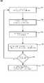
도 1은 본 발명의 실시예들에 따른 실리콘 산화물 필름을 제조하기 위해 선택된 단계들을 나타낸 흐름도이고,
도 2는 본 발명의 실시예들에 따라 기판 갭에 실리콘 산화물 필름을 형성하기 위해 선택된 단계들을 나타낸 다른 흐름도이며,
도 3은 본 발명의 실시예들에 따라 실리콘-함유 필름들로부터 획득된 FTIR 스펙트럼들의 그래프이고,
도 4는 본 발명의 실시예들에 따른 기판 프로세싱 시스템을 도시하며,
도 5a는 본 발명의 실시예들에 따른 기판 프로세싱 챔버를 도시하며,
도 5b는 본 발명의 실시예들에 따른 기판 프로세싱 챔버의 샤워헤드를 도시한다.
유전체 층을 형성하는 방법들이 설명된다. 그러한 방법들은 실리콘-함유 전구체를 플라즈마 유출물과 혼합하는 단계, 및 실리콘-및-질소-함유 층을 기판 상에 증착하는 단계를 포함한다. 실리콘-및-질소-함유 층은 실리콘-및-질소-함유 층을 증착하기 위해서 사용된 동일한 기판 프로세싱 영역에서의 오존-함유 분위기에서의 경화에 의해 실리콘-및-산소-함유 층으로 변환된다. 다른 실리콘-및-질소-함유 층이 실리콘-및-산소-함유 층 상에 증착될 수 있고 그리고 기판 프로세싱 영역으로부터 기판을 제거하지 않고도 층들의 스택이 모두 오존에서 다시 경화될 수 있다. 정수배의 증착-경화 사이클들 후에, 실리콘-및-산소-함유 층들의 스택의 변환체가 산소-함유 환경에서 더 높은 온도에서 어닐링될 수 있다.
전체적으로 정확할 수 있거나 또는 정확하지 않을 수 있는 가설적인 메커니즘들에 청구항들의 커버리지를 결합하지 않고, 일부 세부사항들에 대한 논의가 유익하다는 것이 입증될 수 있다. 비교적 낮은 기판 온도를 유지하면서 증착된 상태 그대로의(as-deposited) 실리콘-및-질소-함유 필름을 오존에 노출시키는 것은, 산소-함유 환경에서 비교적 높은 기판 온도로 기판을 어닐링만 하는 경우보다 산소 함량을 증가시킨다. 이는 라디칼-질소 전구체와 무-탄소 실리콘-및-질소-함유 전구체를 혼합함으로써 실리콘-및-질소 필름의 증착에 의해 생성되는 비교적 개방형 네트워크로 인한 것일 수 있다. 개방형 네트워크는 오존이 필름 내부로 더 깊이 침투하도록, 기판 방향으로의 산화물 변환을 연장한다. 높은 온도에서 변환을 수행하는 것은, 표면 부근에서 네트워크를 폐쇄할 수 있고, 이에 따라, 변환의 물리적 범위를 제한하게 된다.
오존의 반응성은 분자 산소의 반응성과 원자 산소의 반응성 사이에 놓인다. 분자 산소는 산화를 활성화시키기 위해 더 높은 온도를 필요로 하며, 이는 표면 부근에서 개방형 실리콘-및-질소 네트워크의 폐쇄를 초래하게 된다. 이 폐쇄는 실리콘-및-질소-함유 층의 더 깊은 부분들에서의 산화를 바람직하지 않게 제한한다. 원자 산소는 낮은 온도들에서 너무 쉽게 반응하여 마찬가지로 네트워크를 폐쇄할 수 있다. 오존은 개방형 네트워크로 깊게 침투하기 위한 안정성을 제공하는 것으로 밝혀졌으나, 산화를 촉진하기 위해 높은 온도를 필요로 하지 않는다. 이제, 실리콘 산화물 층을 형성하는 시스템들 및 방법들에 대한 추가적인 세부사항들이 설명될 것이다.
수소 및 질소를 대체할 수 있는 오존의 이론적인 능력에 비추어 볼 때, 이는 오존 경화가 증착 영역 내에서 발생할 수 있게, 적은 가열로 또는 가열 없이 오존 경화를 수행하는 것이 가능하는 것을 나타낸다. 이제, 일체화된 오존-경화를 사용하여 실리콘 산화물을 형성하는 방법들 및 시스템에 관한 추가적인 세부사항들이 설명될 것이다.
예시적 실리콘 산화물 형성 프로세스
도 1은 본 발명의 실시예들에 따른 실리콘 산화물 필름들의 제조 방법들(100)에서 선택된 단계들을 나타낸 흐름도이다. 방법(100)은 기판 프로세싱 영역에 무-탄소 실리콘 전구체를 제공하는 단계(102)를 포함한다. 무-탄소 실리콘 전구체는, 다른 부류들(classes)의 실리콘 전구체들 중, 예컨대, 실리콘-및-질소 전구체, 실리콘-및-수소 전구체, 또는 실리콘-질소-및-수소-함유 전구체일 수 있다. 실리콘 전구체는 무-탄소일 뿐만 아니라 무-산소일 수 있다. 산소의 결핍은 전구체들로부터 형성된 실리콘-및-질소 층에서 실라놀(Si-OH) 기들의 더 낮은 농도를 야기한다. 증착된 필름에서 과잉 실라놀 잔기들(moieties)은 증착된 층으로부터 히드록실(-OH) 잔기들을 제거하는 증착후 단계들 동안 공극율과 수축율의 증대를 유발할 수 있다.
무-탄소 실리콘 전구체들의 특정 예들은 다른 시릴-아민들 중 H2N(SiH3), HN(SiH3)2 및 N(SiH3)3와 같은 시릴-아민들을 포함할 수 있다. 시릴-아민의 유량들은 여러 실시예들에서 약 200sccm 또는 그 초과, 약 300sccm 또는 그 초과, 또는 약 500sccm 또는 그 초과일 수 있다. 본 명세서에서 제시된 모든 유량들은 이중 챔버 기판 프로세싱 시스템에 적용된다. 단일 웨이퍼 시스템들은 이 유량들의 절반을 필요로 할 것이며, 다른 웨이퍼 크기들은 프로세싱되는 영역에 의해 스케일링되는 유량들을 필요로 할 것이다. 이 시릴-아민들은 캐리어 가스들, 반응 가스들 또는 이둘 모두로서 작용할 수 있는 추가의 가스들과 혼합될 수 있다. 추가의 가스들의 예들은, 다른 가스들 중에서도, H2, N2, NH3, He 및 Ar을 포함할 수 있다. 또한, 무-탄소 실리콘 전구체들의 예들은 실란(SiH4) 단독, 또는 다른 실리콘-함유 가스(예컨대, N(SiH3)3), 수소-함유 가스(예컨대, H2), 및/또는 질소-함유 가스(예컨대, N2, NH3)와 혼합된 실란을 포함할 수도 있다. 또한, 무-탄소 실리콘 전구체들은 디실란, 트리실란, 보다 고차원의(higher-order) 실란들, 및 염소화된 실란들의, 이들 단독 또는 서로 간의 조합 또는 전술한 무-탄소 실리콘 전구체들과의 조합을 포함할 수 있다. 일반적으로 말해서, 무-탄소 실리콘 전구체들이 사용될 때 보다 필름들이 더 많이 수축할 것이라는 경고(caveat)와 함께, 탄소를 포함하는 실리콘 전구체들이 또한 사용될 수 있다.
또한, 기판 프로세싱 영역에 라디칼-질소 전구체가 제공될 수 있다(104). 라디칼-질소 전구체는 더 안정한 질소 전구체로부터 기판 프로세싱 영역의 외부에서 발생된 질소-라디칼-함유 전구체이다. 예컨대, NH3, H2 및/또는 N2를 함유한 안정한 질소 전구체 화합물이 프로세싱 챔버 외부의 원격 플라즈마 시스템(RPS) 또는 챔버 플라즈마 영역에서 활성화되어 라디칼-질소 전구체를 형성할 수 있으며, 그 후, 라디칼-질소 전구체는 기판 프로세싱 영역 내로 운반된다. 안정한 질소 전구체의 유량은 여러 실시예들에서 약 300sccm 또는 그 초과, 약 500sccm 또는 그 초과, 또는 약 700sccm 또는 그 초과일 수 있다. 챔버 플라즈마 영역에서 생성된 라디칼-질소 전구체는 ·N, ·NH, ·NH2 등 중 하나 또는 그 초과의 것일 수 있으며, 또한 플라즈마에서 형성된 이온화된 종들을 수반할 수도 있다.
일반적으로 말해서, 실리콘-및-질소-함유 층들을 생성하기 위해 다른 라디칼 전구체이 사용될 수 있다. 라디칼 전구체들은 질소를 포함할 수 있거나 또는 포함하지 않을 수 있다. 만약 질소가 라디칼 전구체에 존재하지 않는다면, 질소는 실리콘-함유 전구체에 의해서 공급될 것이다. 질소는, 본 발명의 실시예들에서, 양자 모두의 경우에서 존재할 수 있다. 이러한 탄력성(flexibility)의 결과로서, 라디칼 전구체는 플라즈마 유출물들로서 보다 일반적으로 지칭될 수 있다. 유사하게, (질소가 존재할 수 있거나 또는 존재하지 않을 수 있기 때문에) 플라즈마 유출물을 생성하기 위해서 플라즈마 영역 내로 유동되는 안정한 질소 전구체가 본 명세서에서 일반적으로 안정한 가스로 지칭될 수 있다.
챔버 플라즈마 영역을 채용하는 실시예들에서, 라디칼-질소 전구체는 증착 기판(예컨대, 반도체 웨이퍼) 상에 실리콘-및-질소 층을 증착하기 위해 전구체들이 혼합되고 반응하는 증착 영역으로부터 구획된 기판 프로세싱 영역의 섹션에서 발생된다. 또한, 상기 라디칼-질소 전구체는 수소(H2), 질소(N2), 헬륨 등과 같은 캐리어 가스에 의해 수반될 수 있다. 상기 기판 프로세싱 영역은, 실리콘-및-질소-함유 층의 성장 중에, 그리고 낮은 온도의 오존 경화 동안에, 본 명세서에서, "무-플라즈마"라 기재될 수 있다. "무-플라즈마"는 반드시 영역에 플라즈마가 전혀 없다는 것을 의미하지는 않는다. 챔버 플라즈마 영역에서 플라즈마 경계들을 정의하기 어렵고, 샤워헤드의 개구들을 통해 기판 프로세싱 영역으로 침범할 수 있다. 유도적으로 커플링된 플라즈마의 경우, 소량의 이온화가 기판 프로세싱 영역 내에서 직접적으로 실시될 수 있다. 또한, 형성되는 필름의 유동성 특성을 제거하지 않고, 기판 프로세싱 영역에서 낮은 세기(intensity)의 플라즈마가 생성될 수 있다. 라디칼 질소 전구체의 생성 동안 챔버 플라즈마 영역 보다 훨씬 더 낮은 세기의 이온 밀도를 가진 플라즈마에 대한 모든 내용(causes)들은 본 명세서에 사용된 바와 같이 "무-플라즈마"의 범위를 벗어나지 않는다.
기판 프로세싱 영역에서, 무-탄소 실리콘 전구체와 라디칼-질소 전구체가 혼합되고 반응하여 증착 기판 상에 실리콘-및-질소-함유 필름이 증착된다(106). 증착된 실리콘-및-질소-함유 필름은 실시예들에서 몇몇 레시피 조합으로 컨포멀하게(conformally) 증착될 수 있다. 다른 실시예들에서, 증착된 실리콘-및-질소-함유 필름은 종래의 실리콘 질화물(Si3N4) 필름 증착 기술들과는 다른 유동성 특성들을 갖는다. 형성(formation)의 유동성 특성은 필름이 기판의 증착 표면 상의 좁은 갭들, 트렌치들 및 다른 구조물로 흘러들어갈 수 있도록 한다. 일반적으로 말해서, 보다 높은 라디칼-질소 플럭스들은 컨포멀한(conformal) 증착을 초래하는 한편, 보다 낮은 플럭스들은 유동성 증착을 초래한다.
유동성은 라디칼-질소 전구체들과 무-탄소 실리콘 전구체의 혼합으로 인한 다양한 특성들 때문일 수 있다. 이 특성들은 증착된 필름에서의 상당한 수소 컴포넌트 및/또는 단쇄형(short chained) 폴리실라잔 폴리머들의 존재를 포함할 수 있다. 이러한 단쇄들이 성장하고 네트워킹되어, 필름 형성 동안 그리고 그 후에 더 치밀한 유전체 재료를 형성한다. 예를 들면, 증착된 필름은 실라잔 타입의 Si-NH-Si 백본(backbone)(즉, Si-N-H 필름)을 가질 수 있다. 실리콘 전구체와 라디칼-질소 전구체 모두가 무-탄소인 경우, 증착되는 실리콘-및-질소-함유 필름 또한 실질적으로 무-탄소이다. 물론, "무-탄소"는 반드시 필름이 소량의 탄소도 갖고 있지 않다라는 것을 의미하지는 않는다. 탄소 오염물들은 증착된 실리콘-및-질소 전구체 상태가 되는 전구체 재료들에 존재할 수 있다. 그러나, 이러한 탄소 불순물들의 양은 탄소 잔기(예컨대, TEOS, TMDSO 등)를 가진 실리콘 전구체에서 발견될 것보다 훨씬 더 적다.
실리콘-및-질소-함유 층의 증착 이후, 증착 기판은 오존-함유 분위기에서 경화될 수 있다(108). 증착-후 기판은 경화를 위해서 동일한 기판 프로세싱 영역 내에서 유지된다. 처리량을 유지하기 위해서, 기판의 경화 온도는 실리콘-및-질소-함유 필름의 형성 동안의 기판 온도와 대략적으로 동일할 수 있다. 대안적으로, 기판을 가열된 페이스플레이트 또는 샤워헤드에 보다 더 근접되게 상승시킴으로써, 경화 작업 중에 온도가 상승될 수 있다. 경화 작업 동안에 기판의 온도는 여러 실시예들에서 120℃ 미만, 100℃ 미만, 90℃ 미만, 80℃ 미만, 또는 70℃ 미만일 수 있다. 여러 실시예들에서, 기판의 온도는 증착 동안의 기판 온도 보다 더 높을 수 있고, 50℃ 보다 더 높을 수 있고, 60℃ 보다 더 높을 수 있고, 70℃ 보다 더 높을 수 있고, 또는 80℃ 보다 더 높을 수 있다. 추가적으로 개시된 실시예들에 따라, 기판 온도의 추가적인 범위들을 형성하기 위해, 임의의 상한들(upper bounds)이 임의의 하한들(lower bounds)과 조합될 수 있다.
비교적 높은 농도의 원자 산소가 생성되는 것을 방지하기 위해서, 경화 작업 동안에 기판 프로세싱 영역은 무-플라즈마일 수 있다. 원자 산소의 존재가 실리콘-및-질소-함유 층의 비교적 개방형 네트워크를 조기에 폐쇄할 수 있을 것이다. 인접 표면 네트워크를 폐쇄하고 표면 산화를 저해할 수 있는 원자 산소를 발생시키지 않도록 하기 위해, 실시예들에서, 기판 프로세싱 영역에 플라즈마가 존재하지 않는다. 경화 단계 동안 기판 프로세싱 영역 내로의 오존의 유량은 약 200sccm 또는 그 초과, 약 300sccm 또는 그 초과, 또는 500sccm 또는 그 초과일 수 있다. 경화 단계 동안의 오존의 부분 압력은 약 10Torr 또는 그 초과, 약 20Torr 또는 그 초과, 또는 약 40Torr 또는 그 초과일 수 있다. 일부 조건들(예컨대, 약 100℃ 내지 약 200℃의 기판 온도들 사이에서)하에서, 변환이 실질적으로 완료되는 것으로 밝혀졌으며, 이에 따라, 실시예들에서 산소-함유 환경에서의 비교적 높은 온도의 어닐링이 불필요할 수 있다.
동일한 기판 프로세싱 영역에서의 경화 작업을 수행하는 것은 복수의 증착-경화 사이클들을 가능하게 하여, 각 사이클 동안에 요구되는 두께를 감소시킨다. 이러한 실시예에서, 경화 작업은 실리콘-및-질소-함유 층의 감소된 두께를 변환시키기 위해서만 필요하다. 이는 오존-함유 환경에 대한 요구조건들을 완화시켜, 원자 산소의 보다 큰 농도를 허용하고 그리고 기판 온도 프로세스 윈도우(window)를 확장한다. 일부 실시예들에서 증착-경화 사이클의 경화 부분 동안에는 플라즈마가 존재한다. 다른 실시예들에서, 기판 프로세싱 영역에 플라즈마가 존재하지 않고 그리고 오존-함유 환경은 적은 농도의 원자 산소만을 포함한다. 여러 실시예들에서, 경화 이전에 실리콘-및-질소-함유 층의 층 두께는 1500Å 미만, 1000Å 미만, 750Å 미만, 또는 500Å 미만이 될 수 있다. 복수의 증착-경화 사이클들로부터 야기되는 조합된 모든 실리콘-및-산소-함유 층들의 스택의 두께는, 주로 용도에 따라서, 실시예들에서 400Å 내지 10,000Å 일 수 있다.
목표로 하는 전체 두께에 도달하였는지의 여부에 관한 결정이 이루어진다(109). 만약 목표에 도달하지 못하였으면, 실리콘-및-산소-함유 필름의 두께가 목표 두께에 다시 비교되기 전에, 다른 증착 작업(102 내지 106) 및 다른 경화 작업(108)이 순차적으로 완료된다. 목표에 도달하면, 기판은 기판 프로세싱 챔버에 남겨지거나 또는 그로부터 제거되어 실리콘 산화물에 대한 추가적인 변환을 위해 어닐링 챔버로 전달될 수 있다.
정수의 증착-경화 사이클들에 이어서, 증착 기판은 산소-함유 분위기에서 어닐링될 수 있다(110). 증착 기판은 산소-함유 분위기가 도입될 때 경화를 위해 사용되는 동일한 기판 프로세싱 영역에 남을 수 있거나, 기판은 산소-함유 분위기가 도입되는 다른 챔버로 전달될 수 있다. 산소-함유 분위기는, 다른 산소-함유 가스들 중, 분자 산소(O2), 오존(O3), 수증기(H2O), 과산화수소(H2O2) 및 질소 산화물(NO, NO2 등)과 같은 하나 또는 그 초과의 산소-함유 가스들을 포함할 수 있다. 산소-함유 분위기는 원자 산소(O), 수산화물들(OH) 등과 같은 라디칼 산소 및 히드록실 종들을 또한 포함할 수 있으며, 이들은 원격적으로 발생되어 기판 챔버로 전달될 수 있다. 또한, 산소-함유 종들의 이온들이 존재할 수 있다. 여러 실시예들에서, 기판의 산소 어닐링 온도는 약 1100℃ 또는 그 미만, 약 1000℃ 또는 그 미만, 약 900℃ 또는 그 미만, 또는 약 800℃ 또는 그 미만일 수 있다. 여러 실시예들에서, 기판의 온도는 약 500℃ 또는 그 초과, 약 600℃ 또는 그 초과, 약 700℃ 또는 그 초과, 또는 약 800℃ 또는 그 초과일 수 있다. 다시 한번, 추가적으로 개시된 실시예들에 따라, 기판 온도에 대한 추가적인 범위들을 형성하기 위해, 임의의 상한들이 임의의 하한들과 조합될 수 있다.
산소 어닐링 동안 기판 프로세싱 영역에 플라즈마가 존재하거나 또는 존재하지 않을 수 있다. CVD 챔버에 진입하는 산소-함유 가스는 기판 프로세싱 영역에 진입하기 전에 활성화된(예컨대, 라디칼화된, 이온화된, 등) 하나 또는 그 초과의 화합물들을 포함할 수 있다. 예를 들어, 산소-함유 가스는, 원격 플라즈마 소오스를 통해, 또는 샤워헤드에 의해 기판 프로세싱 영역으로부터 분리된 챔버 플라즈마 영역을 통해, 더 안정한 전구체 화합물들을 노출함으로써 활성화된, 라디칼 산소 종들, 라디칼 히드록실 종들 등을 포함할 수 있다. 더 안정한 전구체들은 히드록실(OH) 라디칼들 및 이온들을 생성하는 수증기 및 과산화수소(H2O2), 그리고 원자 산소(O) 라디칼들 및 이온들을 생성하는 분자 산소 및/또는 오존을 포함할 수 있다.
경화 및 산소 어닐링 모두의 산소-함유 분위기들은 실리콘-및-질소-함유 필름을 실리콘 산화물(SiO2) 필름으로 변환시키기 위해 산소를 제공한다. 전술한 바와 같이, 실리콘-및-질소-함유 필름에서의 탄소의 결핍은 최종 실리콘 산화물 필름에 현저히 적은 기공들이 형성되는 결과를 초래한다. 이는 또한, 실리콘 산화물로의 변환 동안 필름의 체적 감소(즉, 수축)를 적게 하는 결과를 초래한다. 예컨대, 탄소-함유 실리콘 전구체들로부터 형성되는 실리콘-질소-탄소 층이 실리콘 산화물로 변환될 때 40 vol% 또는 그 초과만큼 수축할 수 있는 경우, 실질적으로 무-탄소 실리콘-및-질소 필름들은 약 15 vol% 또는 그 미만만큼 수축할 수 있다.
이제, 도 2를 참조하면, 본 발명의 실시예들에 따라 기판 갭에 실리콘 산화물 필름을 형성하기 위한 방법들(200)에서 선택된 단계들을 나타낸 다른 흐름도가 도시되어 있다. 방법(200)은 갭을 포함한 기판을 기판 프로세싱 영역으로 전달하는 단계(작업(202))를 포함할 수 있다. 기판은 그 기판 상에 형성된 디바이스 컴포넌트들(예컨대, 트랜지스터들)의 구조와 간격에 대한 복수의 갭들을 가질 수 있다. 갭들은 1:1 보다 훨씬 더 큰 (예컨대, 5:1 또는 그 초과, 6:1 또는 그 초과, 7:1 또는 그 초과, 8:1 또는 그 초과, 9:1 또는 그 초과, 10:1 또는 그 초과, 11:1 또는 그 초과, 12:1 또는 그 초과, 등) 높이 대 폭(즉, H/W)의 종횡비(AR)를 정의하는 높이와 폭을 가질 수 있다. 많은 경우들에서, 높은 AR은 약 90㎚ 내지 약 22㎚ 또는 그 미만까지(예컨대, 약 90㎚ 또는 그 미만, 65㎚ 또는 그 미만, 45㎚ 또는 그 미만, 32㎚ 또는 그 미만, 28㎚ 또는 그 미만, 22㎚ 또는 그 미만, 16㎚ 또는 그 미만 등)의 범위의 작은 갭 폭들에 기인한다.
기판 프로세싱 영역에서 무-탄소 실리콘 전구체가 라디칼-질소 전구체와 혼합된다(작업(204)). 기판 상에 유동성 실리콘-및-질소-함유 층이 증착될 수 있다(작업(206)). 상기 층은 유동성이기 때문에, 상기 층은 충진 재료의 중앙 주변에 공극들 또는 약한 시임들을 생성하지 않고 높은 종횡비들을 갖는 갭을 충진할 수 있다. 예를 들어, 증착되는 유동성 재료는 갭이 완전히 충진되기 전에 갭의 상단을 조기에 막아 갭의 중간에 공극을 남기는 경우가 거의 없다.
이어서, 증착된 상태 그대로의 실리콘-및-질소-함유 층은, 작업들(204 내지 206)에서 수행되는 증착을 위해서 사용되는 동일한 기판 프로세싱 영역에서 경화될 수 있다(작업(208)). 도시된 실시예에서, 복수의 증착-경화 사이클들은 도시되어 있지 않지만, 도 1을 참조하여 도시되고 설명된 반복(repetition)과 유사한 방식으로 수행될 수 있다. 변환이 완료되지 않았다면, 실리콘-및-질소-함유 층을 실리콘 산화물로 변화시키기 위해서 부분적으로 변환된 실리콘-및-산소-함유 층이 산소-함유 분위기에서 어닐링된다(작업(210)). 실리콘 산화물 층을 조밀화하기 위해서, 추가적인 어닐링(미도시)이 더 높은 기판 온도에서의 불활성 분위기에서 실행될 수 있다.
산소-함유 분위기에서 증착된 상태 그대로의 실리콘-및-질소-함유 층의 경화 및 어닐링은 기판 갭을 포함하여 기판 상에 실리콘 산화물 층을 형성한다(208). 실시예들에서, 작업들(208, 210)의 프로세싱 파라미터들은 도 1의 작업들(108, 110)을 참조하여 기재된 것과 동일한 범위들을 가진다. 전술한 바와 같이, 실리콘 산화물 층은, 열처리 단계 전에 당해 층에 존재하는 상당량의 탄소를 포함하는, 탄소-함유 전구체들로 형성된 유사한 층들보다, 기공들이 더 적고 체적 감소가 더 적다. 많은 경우들에서, 체적 감소는 수축하는 실리콘 산화물의 결과로서 갭에 형성되는 공간들을 충진, 치유 또는 그렇지 않으면 제거하기 위해 사후 열처리(post heat treatment) 단계들을 피할 수 있을 정도로 충분히 작다(예컨대, 약 15 vol% 또는 그 미만).
도 3은 본 발명의 실시예들에 따른 실리콘-함유 필름들로부터 획득된 FTIR 스펙트럼들의 그래프이다. 증착된 상태 그대로의 실리콘-및-질소-함유 필름(305)은 수소 및 질소의 존재를 나타내는 908cm-1 - 933cm-1에 근접한 강한 피크 및 835cm-1 - 860cm-1에 근접한 강한 피크를 보여준다. 기판 프로세싱 영역 내부에서 경화된 실리콘-및-질소-함유 필름들에 대한 FTIR 스펙트럼(315) 및 오존 외부에서 경화된 실리콘-및-질소-함유 필름들에 대한 FTIR 스펙트럼(310)이 또한 보여진다. 양자 모두의 경우들에서, 수소와 연관된 피크가 유사하게 감소되고 그리고 다른 피크들도 또한 근접하게 매칭된다(match). 이는, 인-시츄 경화의 더 낮은 온도의 경화가 전용 챔버에서의 경화에 대해서 유사하게 효과적이라는 것을 나타낸다. FTIR 스펙트럼은 또한 8의 증착-경화 사이클들에서 프로세싱되는 실리콘 산화물에 대해 320으로 보여주고, 이는 매우 적은 수소 및 질소가 필름 내에 잔류한다는 것을 나타낸다. 복수의 증착-경화 사이클들과 연관된 FTIR 스펙트럼은 또한 Si-H-N의 실리콘 산화물로의 양호한 변환을 나타내는, 1100cm-1 부근의 매우 강한 산소 피크를 보여준다.
예시적 실리콘 산화물 증착 시스템
본 발명의 실시예들을 실행할 수 있는 증착 챔버들은, 다른 유형들의 챔버들 중에서, 고밀도 플라즈마 화학기상증착(HDP-CVD) 챔버들, 플라즈마 강화 화학기상증착(PECVD) 챔버들, 감압 화학기상증착(SACVD) 챔버들, 및 열적 화학기상증착 챔버들을 포함할 수 있다. 본 발명의 실시예들을 실행할 수 있는 CVD 시스템들의 특정한 예들은, 캘리포니아, 산타 클라라에 소재한 어플라이드 머티어리얼사로부터 입수할 수 있는, CENTURA ULTIMA®HDP-CVD 챔버들/시스템들 및 PRODUCER®RECVD 챔버들/시스템들을 포함한다.
본 발명의 예시적 방법들과 함께 사용될 수 있는 기판 프로세싱 챔버들의 예들은 "유전체 갭충진을 위한 프로세스 챔버"란 명칭으로 루보미르스키 등이 2006년 5월 30일자로 출원하여 본 출원인에게 공동 양도된 미국 가특허 출원번호 제60/803,499호에 도시되고 설명된 것들을 포함할 수 있고, 이의 전체 내용들이 모든 목적들을 위해 인용에 의해 본 명세서에 포함된다. 추가적인 예시적 시스템들은 미국특허 제6,387,207호 및 제6,830,624호에 도시되고 설명된 것들을 포함할 수 있고, 이들 또한 모든 목적들을 위해 인용에 의해 본 명세서에 포함된다.
증착 시스템들의 실시예들은 집적 회로 칩들을 생산하기 위한 대형 제조 시스템들에 통합될 수 있다. 도 4는 개시된 실시예들에 따른 증착, 베이킹(baking) 및 경화 챔버들의 그러한 하나의 시스템(400)을 도시하고 있다. 도면에서, 한 쌍의 FOUP(front opening unified pods)(402)가 기판들(예컨대, 300㎜ 직경의 웨이퍼들)을 공급하고 있으며, 이 기판들은 로봇 암들(404)에 의해 수용되며 웨이퍼 프로세싱 챔버들(408a 내지 408f) 중 하나에 위치되기 전에 낮은 압력의 홀딩 영역(406)에 위치된다. 홀딩 영역(406)으로부터 프로세싱 챔버들(408a 내지 408f)로 그리고 그 역으로 기판 웨이퍼들을 운반하기 위해 제 2 로봇 암(410)이 사용될 수 있다.
프로세싱 챔버들(408a 내지 408f)은 기판 웨이퍼 상에 유동성 유전체 필름을 증착, 어닐링, 경화 및/또는 에칭하기 위한 하나 또는 그 초과의 시스템 컴포넌트들을 포함할 수 있다. 하나의 구성에 있어서, 유동성 유전체 재료를 기판 상에 증착하기 위해 2쌍의 프로세싱 챔버들(예컨대, 408c와 408d, 및 408e와 408f)이 사용될 수 있으며, 증착된 유전체를 어닐링하기 위해 제 3 쌍의 프로세싱 챔버들(예컨대, 408a와 408b)이 사용될 수 있다. 다른 구성에 있어서, 동일한 2쌍의 프로세싱 챔버들(예컨대, 408c와 408d, 및 408e와 408f)이 기판 상에서의 유동성 유전체 필름의 증착과 어닐링 모두를 위해 구성될 수 있는 한편, 제 3 쌍의 챔버들(예컨대, 408a와 408b)이 증착된 필름의 UV 또는 E-빔 경화를 위해 사용될 수 있다. 또 다른 구성에 있어서, 모두 3쌍의 챔버들(예컨대, 408a 내지 408f)이 기판 상에서 유동성 유전체 필름을 증착 및 경화하도록 구성될 수 있고 그리고 각각은 가열된 샤워헤드를 향해서 기판을 상승시키기 위한 승강 핀들로 구성될 수 있으며, 그에 따라 "통합된" 경화 작업에서 온도를 상승시킨다. 또 다른 구성에 있어서, 2쌍의 프로세싱 챔버들(예컨대, 408c와 408d, 및 408e와 408f)은 유동성 유전체의 증착과 UV 또는 E-빔 경화 모두를 위해 사용될 수 있는 한편, 제 3 쌍의 프로세싱 챔버들(예컨대, 408a와 408b)은 유전체 필름의 어닐링을 위해 사용될 수 있다. 개시된 프로세스들 중 임의의 하나 또는 그 초과가 여러 실시예들에 도시된 제조 시스템과 분리된 챔버(들)상에서 실행될 수 있다.
또한, 프로세싱 챔버들(408a 내지 408f) 중 하나 또는 그 초과가 습식 처리 챔버로서 구성될 수 있다. 이 프로세싱 챔버들은 습기를 포함한 분위기에서 유동성 유전체 필름의 가열을 포함한다. 따라서, 시스템(400)의 실시예들은 증착된 유전체 필름에 대한 습식 및 건식 어닐링들 모두를 수행하기 위해 습식 처리 챔버들(408a와 408b)과 어닐링 프로세싱 챔버들(408c와 408d)을 포함할 수 있다.
도 5a는 개시된 실시예들에 따른 기판 프로세싱 챔버(500)이다. 원격 플라즈마 시스템(RPS)(510)은 이후 가스 유입 조립체(511)를 통해 이동하는 가스를 프로세싱할 수 있다. 2개의 분리된 가스 공급 채널들은 가스 유입 조립체(511) 내에서 볼 수 있다. 제 1 채널(512)은 원격 플라즈마 시스템 RPS(510)를 통과하는 가스를 운반하는 반면, 제 2 채널(513)은 RPS(510)를 바이패스한다. 개시된 실시예들에서, 제 1 채널(512)은 프로세스 가스를 위해 사용될 수 있고, 제 2 채널(513)은 처리 가스를 위해 사용될 수 있다. 덮개(또는 전도성 상단부)(521)와 천공된 격벽(553)이 그들 사이의 절연링(524)과 함께 도시되어 있으며, 상기 절연링(524)은 AC 전위가 천공된 격벽(553)에 대해서 덮개(521)에 인가될 수 있도록 한다. 프로세스 가스는 제 1 채널(512)을 통해 챔버 플라즈마 영역(520)으로 이동하며, 챔버 플라즈마 영역(520)에서 플라즈마에 의해 단독으로, 또는 RPS(510)와 조합하여 여기될 수 있다. 챔버 플라즈마 영역(520) 및/또는 RPS(510)의 조합은 본 명세서에서 원격 플라즈마 시스템이라 지칭될 수 있다. (또한, '샤워헤드'라고도 지칭되는) 천공된 격벽(553)은 샤워헤드(553) 아래의 기판 프로세싱 영역(570)으로부터 챔버 플라즈마 영역(520)을 분리시킨다. 샤워헤드(553)는 챔버 플라즈마 영역(520)에 존재하는 플라즈마가 기판 프로세싱 영역(570)의 가스를 직접 여기시키지 않도록 하는 한편, 여기된 종들이 챔버 플라즈마 영역(520)으로부터 기판 프로세싱 영역(570) 내로 이동할 수 있도록 한다.
샤워헤드(553)는 챔버 플라즈마 영역(520)과 기판 프로세싱 영역(570) 사이에 위치되며, 챔버 플라즈마 영역(520) 내부에 생성된 플라즈마 유출물들(전구체들 또는 다른 가스들의 여기된 유도체들)이 복수의 관통홀들(556)을 통과할 수 있도록 하며, 상기 관통홀은 판의 두께를 횡단한다. 또한, 샤워헤드(553)는 (실리콘-함유 전구체와 같이) 증기 또는 가스 형태의 전구체로 충진될 수 있는 하나 또는 그 초과의 빈 공간들(hollow volumes)(551)을 갖고, 상기 빈 공간은 작은 홀들(555)을 통해 기판 프로세싱 영역(570)으로 통과하나, 챔버 플라즈마 영역(520)으로는 직접 통과되지 않는다. 개시된 본 실시예에서, 샤워헤드(553)는 관통홀들(556)의 최소 직경(550)의 길이보다 더 두껍다. 챔버 플라즈마 영역(520)으로부터 기판 프로세싱 영역(570)으로 침투하는 여기된 종들의 상당한(significant) 농도를 유지하기 위해, 관통홀들의 최소 직경(550)의 길이(526)는 샤워헤드(553)를 관통하는 중간에 관통홀들(556)의 더 큰 직경 부분들을 형성함으로써 제한될 수 있다. 개시된 실시예들에서, 관통홀들(556)의 최소 직경(550)의 길이는 관통홀들(556)의 최소 직경과 같은 크기(same order of magnitude)와 동일하거나 또는 그보다 작을 수 있다.
도시된 실시예에서, 샤워헤드(553)는 산소, 수소 및/또는 질소를 함유한 프로세스 가스들 및/또는 챔버 플라즈마 영역(520)에서 플라즈마에 의해 여기될 때 그러한 프로세스 가스들의 플라즈마 유출물들을 (관통홀들(556)을 통해) 분배할 수 있다. 실시예들에서, 제 1 채널(512)을 통해 RPS(510) 및/또는 챔버 플라즈마 영역(520)으로 유입되는 프로세스 가스는 산소(O2), 오존(O3), N2O, NO, NO2, NH3, 그리고 N2H4를 포함하는 NxHy, 실란, 디실란, TSA 및 DSA 중 하나 또는 그 초과를 함유할 수 있다. 또한, 프로세스 가스는 헬륨, 아르곤, 질소(N2) 등과 같은 캐리어 가스를 포함할 수 있다. 또한, 제 2 채널(513)은 성장하거나 또는 증착된 상태 그대로의 필름으로부터 원하지 않는 컴포넌트를 제거하기 위해서, 사용된 프로세스 가스 및/또는 캐리어 가스, 및/또는 필름-경화 가스를 전달할 수 있다. 플라즈마 유출물들은 프로세스 가스의 이온화된 유도체들 또는 중성의 유도체들을 포함할 수 있으며, 유입된 프로세스 가스의 원자 구성성분들(constituents)을 지칭하는 라디칼-산소 전구체 및/또는 라디칼-질소 전구체로서 본 명세서에서 또한 지칭될 수 있다. 샤워헤드(553)는 챔버 플라즈마 영역(520) 내의 플라즈마로부터 간접적으로 또는 (저항식으로 또는 매립형 채널을 통과하는 열전달 유체를 사용하여) 직접적으로 가열될 수 있다. 어느 방식에서든, 가열된 샤워헤드(553)에 더 가깝게 기판을 상승시키고 일단 경화 작업이 완료되면 기판을 다시 하강시킴으로써 통합된 경화 단계 동안 기판 온도가 상승될 수 있다.
실시예들에서, 관통홀들(556)의 수는 약 60 내지 약 2000개일 수 있다. 관통홀들(556)은 다양한 형상들을 가질 수 있으나, 가장 용이하게 원형으로 제조된다. 개시된 실시예에서, 관통홀들(556)의 최소 직경(550)은 약 0.5㎜ 내지 약 20㎜ 이거나, 약 1㎜ 내지 약 6㎜일 수 있다. 또한, 관통홀들의 단면 형상을 선택하는 것은 자유이며 관통홀들의 단면 형상은 원뿔형, 원통형 또는 이 두 가지 형상들의 조합으로 제조될 수 있다. 여러 실시예에서, 가스를 기판 프로세싱 영역(570)으로 유입시키기 위해 사용되는 작은 홀들(555)의 수는 약 100 내지 약 5000개 또는 약 500 내지 약 2000개일 수 있다. 작은 홀들(555)의 직경은 약 0.1㎜ 내지 약 2㎜일 수 있다.
도 5b는 개시된 실시예들에 따른 프로세싱 챔버와 함께 사용하기 위한 샤워헤드(553)의 저면도이다. 샤워헤드(553)는 도 5a에 도시된 샤워헤드와 대응한다. 관통홀들(556)은 샤워헤드(553)의 바닥에서 더 큰 내부 직경(ID)을 갖고 상단에서 더 작은 ID을 갖는 것으로 도시되어 있다. 작은 홀들(555)이 샤워헤드의 표면에 걸쳐, 심지어는 관통홀들(556) 사이에서도, 실질적으로 균일하게 분포되어 있으며, 이는 보다 더 균일한 혼합을 제공하는 것을 돕는다.
샤워헤드(553)의 관통홀들(556)을 통해 도달하는 플라즈마 유출물들이 빈 공간들(551)로부터 기원하는 작은 홀들(555)을 통해 도달하는 실리콘-함유 전구체와 조합될 때, 기판 프로세싱 영역(570) 내부의 페데스탈(미도시)에 의해 지지된 기판 상에 예시적 필름이 생성된다. 기판 프로세싱 영역(570)이 경화와 같은 다른 프로세스들을 위해 플라즈마를 지원하도록 설비될 수 있으나, 예시적 필름의 성장 동안 플라즈마가 존재하지 않는다.
플라즈마는 샤워헤드(553) 위의 챔버 플라즈마 영역(520) 또는 샤워헤드(553) 아래의 기판 프로세싱 영역(570)에서 점화될 수 있다. 질소-및-수소-함유 가스의 유입으로부터 라디칼 질소 전구체를 생성하기 위해서 플라즈마가 챔버 플라즈마 영역(520)에 존재한다. 증착 동안 챔버 플라즈마 영역(520)에서 플라즈마를 점화하기 위해, 샤워헤드(553)와 프로세싱 챔버의 전도성 상단부(521) 사이에, 통상적으로 무선 주파수(RF) 범위인, AC 전압이 인가된다. RF 전원공급장치는 13.56㎒의 높은 RF 주파수를 발생시키지만, 또한 다른 주파수들을 단독으로 발생시키거나, 13.56㎒ 주파수와 조합하여 발생시킬 수도 있다.
기판 프로세싱 영역(570)과 접한 내부 표면들을 세척하거나 또는 필름을 경화시키기 위해 기판 프로세싱 영역(570)에서 하위 플라즈마가 턴온될 때, 상위 플라즈마는 저전력으로 유지되거나 또는 무전력으로 유지될 수 있다. 기판 프로세싱 영역(570)에서의 플라즈마는 샤워헤드(553)와 챔버의 페데스탈 또는 바닥 사이에 AC 전압을 인가함으로써 점화된다. 플라즈마가 존재할 때, 세척 가스가 기판 프로세싱 영역(570)으로 유입될 수 있다.
페데스탈은 열교환 채널을 가질 수 있으며 이 열교환 채널을 통해 열교환 유체가 흘러 기판의 온도를 제어할 수 있다. 이 구성은 기판 온도가 비교적 낮은 온도들(실온 내지 약 120℃까지)로 유지되도록 냉각 또는 가열될 수 있도록 한다. 열교환 유체는 에틸렌 글리콜과 물을 포함할 수 있다. 또한, 페데스탈(바람직하게, 알루미늄, 세라믹, 또는 이들의 조합)의 웨이퍼 지지 플래터(platter)는, 평행한 동심원들의 형태로 2개의 완전 턴들(full turns)을 만들도록 구성된 내장식 단일 루프 히터 부재를 사용하여 비교적 고온들(약 120℃ 내지 약 1100℃)을 달성하기 위해 저항식으로 가열될 수 있다. 히터 부재의 바깥 부분은 지지 플래터의 원주에 인접하여 연장될 수 있는 반면, 안쪽 부분은 더 작은 반경을 가진 동심원의 경로 상으로 연장한다. 상기 히터 부재에 대한 배선은 페데스탈의 스템을 통과한다.
기판 프로세싱 시스템은 시스템 컨트롤러에 의해 제어된다. 예시적 실시예에서, 시스템 컨트롤러는 하드 디스크 드라이브, 플로피 디스크 드라이브 및 프로세서를 포함한다. 프로세서는 단일 보드 컴퓨터(SBC), 아날로그 및 디지털 입력/출력 보드들, 인터페이스 보드들 및 스텝퍼 모터 컨트롤러 보드들을 포함한다. CVD 시스템의 다양한 부품들은 보드, 카드 케이지 및 커넥터 치수들 및 유형들을 정의하는 VME(Versa Modular European) 표준을 따른다. 또한, VME 표준은 16비트 데이타 버스와 24비트 어드레스 버스를 가진 것으로서 버스 구조를 정의한다.
시스템 컨트롤러는 CVD 기계의 모든 활동들을 제어한다. 시스템 컨트롤러는 컴퓨터-판독가능한 매체 내에 저장된 컴퓨터 프로그램인 시스템 제어 소프트웨어를 실행한다. 바람직하게, 상기 매체는 하드 디스크 드라이브이나, 그러한 매체는 또한 다른 종류들의 메모리일 수도 있다. 컴퓨터 프로그램은 타이밍, 가스들의 혼합물, 챔버 압력, 챔버 온도, RF 전력 레벨들, 서셉터 위치, 및 특정 프로세스의 다른 파라미터들을 지시하는 명령들의 세트들을 포함한다. 예를 들어, 플로피 디스크 또는 다른 또다른 적합한 드라이브를 포함하는 다른 메모리 디바이스들 상에 저장된 다른 컴퓨터 프로그램들이 시스템 컨트롤러를 명령하는데 또한 사용될 수 있다.
기판 상에 필름 스택을 적층하기 위한 프로세스 또는 챔버를 세척하기 위한 프로세스는 시스템 컨트롤러에 의해 실행되는 컴퓨터 프로그램 물건을 사용하여 구현될 수 있다. 컴퓨터 프로그램 코드는 임의의 종래의 컴퓨터 판독 가능한 프로그래밍 언어, 예를 들어 68000 어셈블리 언어, C, C++, 파스칼, 포트란 또는 기타 언어들로 기록될 수 있다. 적합한 프로그램 코드가 종래의 텍스트 에디터를 사용하여 단일 파일 또는 다중 파일들로 입력되며, 컴퓨터의 메모리 시스템과 같은 컴퓨터 사용가능한 매체에 저장 또는 내장된다. 입력된 코드 텍스트가 고차원 언어라면, 코드는 컴파일되고 그 결과적인 컴파일러 코드가 프리컴파일드 Microsoft Windows® 라이브러리 루틴들의 목적 코드와 연결된다. 연결된, 컴파일드 목적 코드를 실행하기 위해, 시스템 사용자는 목적 코드를 호출하여, 컴퓨터 시스템이 메모리에 코드를 로딩하게 한다. 그 후 CPU는 코드를 판독하고 실행하여 프로그램에서 확인된 임무들을 수행한다.
사용자와 컨트롤러 사이의 인터페이스는 평판형 터치 감응형 모니터를 통한다. 바람직한 실시예에서, 2개의 모니터들이 사용되는데, 하나는 작업자들을 위해서 클린룸 벽(clean room wall)에 장착되고 다른 하나는 서비스 기술자들을 위해서 벽의 뒤에 장착된다. 2개의 모니터들은 동일한 정보를 동시에 디스플레이할 수 있지만, 그 경우, 한번에 단지 하나만 입력을 받아들인다. 특정 스크린 또는 기능을 선택하기 위해서, 작업자는 터치 감응형 모니터의 지정된 영역을 터치한다. 터치된 영역은 그의 하이라이트된 색을 변화시키거나, 새로운 매뉴 또는 스크린이 디스플레이되어, 터치 감응형 모니터와 작업자 사이의 통신을 확인한다. 그 밖의 디바이스들, 예컨대, 키보드, 마우스, 또는 다른 포인팅 또는 통신 디바이스가 터치 감응형 모니터 대신 또는 그에 부가하여 사용되어 사용자가 시스템 컨트롤러와 통신할 수 있게 할 수 있다.
본 명세서에서 사용된 바와 같이, "기판"은 그 위에 층들이 형성되거나 또는 형성되지 않은 지지 기판일 수 있다. 지지 기판은 절연체이거나, 다양한 도핑 농도들 및 프로파일들을 가진 반도체일 수 있으며, 예컨대, 집적 회로들의 제조에 사용되는 유형의 반도체 기판일 수 있다. "실리콘 산화물"의 층은 질소, 수소, 탄소 등과 같은 다른 원소 구성성분의 마이너리티(minority) 농도들을 포함할 수 있다. 본 발명의 일부 실시예들에서, 실리콘 산화물은 본질적으로 실리콘과 산소로 구성된다. "여기된 상태"의 가스는 가스 분자들 중 적어도 일부가 진동-여기되거나, 분해되거나 그리고/또는 이온화된 상태들에 있는 가스를 나타낸다. 가스(또는 전구체)는 둘 또는 그 초과의 가스들(전구체들)의 조합일 수 있다. "트랜치"라는 용어는 에칭된 기하형상이 큰 수평적 종횡비를 갖는다는 암시 없이 전체적으로 사용되었다. 표면 위에서 봤을 때, 트랜치들은 원형, 타원형, 다각형, 직사각형, 또는 다양한 다른 형상들을 나타낼 수 있다. "비아"라는 용어는 수직한 전기적 접속을 형성하기 위해 금속으로 충진되거나 또는 충진되지 않을 수 있는 낮은 종횡비 트랜치를 지칭하기 위해 사용된다. "전구체"라는 용어는 표면으로부터 물질을 제거하거나 또는 물질을 증착하기 위한 반응의 일부에 참여하는 임의의 프로세스 가스(또는 증발된 액적(liquid droplet))를 지칭하기 위해서 사용된다.
몇 개의 실시예들을 개시하였지만, 본 발명의 사상을 벗어나지 않고 다양한 변형들, 대안적 구성들, 및 등가물들이 사용될 수 있다는 것이 당업자들에 의해 인식될 것이다. 부가적으로, 본 발명이 불필요하게 불명료해지는 것을 방지하기 위해서, 많은 수의 공지된 프로세스들 및 부재들은 설명되지는 않았다. 따라서, 상기 설명은 본 발명의 범주를 제한하는 것으로 간주되어서는 안된다.
값들의 범위가 제공될 때, 문맥에 달리 명확하게 설명되지 않는다면, 이들 범위의 상한치 및 하한치 사이에서, 하한치 유니트(unit)의 1/10 까지, 중간 값이 또한 구체적으로 개시된 것임이 이해된다. 임의의 언급된 값 또는 언급된 범위 내의 중간 값과 임의의 다른 언급된 또는 그 언급된 범위내의 중간 값들 사이의 각각의 더 작은 범위가 포함된다. 이들 작은 범위들의 상한치 및 하한치는 독립적으로 범위에 포함되거나 또는 범위에서 배제될 수 있으며, 언급된 범위에서 임의의 특별히 배제된 한계치에 따라 더 작은 범위들 내에 한계치들 중 하나 또는 둘 다가 포함되거나 또는 둘 다가 포함되지 않는 경우 각각의 범위가 또한 본 발명 내에 포함된다. 언급된 범위가 한계치들 중 하나 또는 둘 다를 포함하는 경우, 이들 포함된 한계치들 중 어느 하나 또는 둘 다를 배제하는 범위들이 또한 포함된다.
본 명세서 및 첨부되는 청구항들에서 사용되는 바와 같이, 단수 형태("a" "an" 및 "상기(the)")는 문맥에 달리 명확하게 설명되지 않는다면 복수의 대상들을 포함한다. 따라서, 예를 들어, "프로세스(process)"라는 참조는 복수의 이러한 프로세스들을 포함하며, "전구체(the precursor)"라는 참조는 당업자들에게 알려진 하나 또는 그 초과의 전구체 및 등가물들에 대한 참조를 포함하는 식이다.
또한, 본 명세서 및 하기 청구항들에서 사용되는 포함("comprise," "comprising," "include," "including," 및 "includes")이라는 단어는 언급된 피쳐들, 정수들, 컴포넌트들 또는 단계들의 존재를 특정하게 의도되나, 이는 하나 또는 그 초과의 다른 피쳐들, 정수들, 컴포넌트들, 단계들, 동작들 또는 그룹들의 존재 또는 부가를 배제하는 것은 아니다.
Claims (20)
- 기판 프로세싱 챔버의 기판 프로세싱 영역에서 기판 상에 실리콘-및-산소-함유 층을 형성하는 방법으로서,
상기 기판 프로세싱 영역에서 상기 기판 상에 실리콘-및-질소-함유 층을 형성하는 단계 ― 상기 실리콘-및-질소-함유 층을 형성하는 단계는,
플라즈마 유출물들을 생성하기 위해서 안정한 가스를 플라즈마 영역 내로 유동시키는 단계,
무-플라즈마 기판 프로세싱 영역에서 상기 플라즈마 유출물들과 실리콘-함유 전구체를 조합하는 단계 ― 상기 실리콘-함유 전구체는 무-탄소임 ―, 그리고
상기 기판 상에 실리콘-및-질소-함유 층을 증착하는 단계
를 포함함 ― ; 및
상기 실리콘-및-산소-함유 층을 형성하기 위해서, 동일한 기판 프로세싱 영역에서의 오존-함유 분위기에서 상기 실리콘-및-질소-함유 층을 경화시키는 단계
를 포함하며, 경화 작업 동안 기판의 온도는 상기 실리콘-및-질소-함유 층을 증착하는 작업 동안의 온도보다 50 ℃ 미만만큼 더 높은, 실리콘-및-산소-함유 층을 형성하는 방법. - 제 1 항에 있어서,
상기 기판 프로세싱 영역에서 상기 기판 상에 제 2 실리콘-및-질소-함유 층을 형성하는 단계 ― 상기 제 2 실리콘-및-질소-함유 층을 형성하는 단계는,
플라즈마 유출물들을 생성하기 위해서 상기 안정한 가스를 상기 플라즈마 영역 내로 유동시키는 단계,
상기 기판 프로세싱 영역에서 상기 플라즈마 유출물들과 실리콘-함유 전구체를 조합하는 단계, 및
상기 기판 프로세싱 영역에서 상기 기판 상에 상기 제 2 실리콘-및-질소-함유 층을 증착하는 단계
를 포함함 ― ; 및
상기 기판 프로세싱 영역에서의 오존-함유 분위기에서 상기 제 2 실리콘-및-질소-함유 층을 경화시키는 단계
를 더 포함하는, 실리콘-및-산소-함유 층을 형성하는 방법. - 제 1 항에 있어서,
상기 기판 프로세싱 영역은 상기 실리콘-함유 전구체의 직접적인 플라즈마-여기를 방지하기 위해서 상기 실리콘-및-질소-함유 층을 형성하는 작업 동안에 무-플라즈마인, 실리콘-및-산소-함유 층을 형성하는 방법. - 제 1 항에 있어서,
상기 기판 프로세싱 영역은 상기 실리콘-및-질소-함유 층을 경화하는 작업 동안에 무-플라즈마인, 실리콘-및-산소-함유 층을 형성하는 방법. - 제 1 항에 있어서,
상기 실리콘-및-질소-함유 층을 증착하는 작업 동안의 기판 온도는 100℃ 미만인, 실리콘-및-산소-함유 층을 형성하는 방법. - 제 1 항에 있어서,
상기 경화 작업 동안의 기판 온도는 200℃ 미만인, 실리콘-및-산소-함유 층을 형성하는 방법. - 제 1 항에 있어서,
상기 실리콘-및-질소-함유 층의 두께는 1500Å 또는 그 미만인, 실리콘-및-산소-함유 층을 형성하는 방법. - 제 1 항에 있어서,
상기 경화 작업 동안에 상기 기판을 가열하기 위해서, 상기 기판은 가열된 샤워헤드를 향해서 상승되는, 실리콘-및-산소-함유 층을 형성하는 방법. - 제 1 항에 있어서,
상기 안정한 가스는 질소-및-수소-함유 가스이고 그리고 상기 플라즈마 유출물들은 라디칼-질소 전구체를 포함하는, 실리콘-및-산소-함유 층을 형성하는 방법. - 제 9 항에 있어서,
상기 질소-및-수소-함유 가스는 암모니아를 포함하는, 실리콘-및-산소-함유 층을 형성하는 방법. - 제 1 항에 있어서,
상기 실리콘-함유 전구체는 실리콘-및-질소-함유 전구체를 포함하는, 실리콘-및-산소-함유 층을 형성하는 방법. - 제 1 항에 있어서,
상기 실리콘-함유 전구체는 N(SiH3)3를 포함하는, 실리콘-및-산소-함유 층을 형성하는 방법. - 제 1 항에 있어서,
상기 실리콘-및-질소-함유 층은 무-탄소 Si-N-H 층을 포함하는, 실리콘-및-산소-함유 층을 형성하는 방법. - 제 1 항에 있어서,
상기 기판은 패터닝되고 그리고 45nm 또는 그 미만의 폭을 가지는 트렌치를 포함하고, 상기 트렌치 내에 형성된 상기 실리콘-및-산소-함유 층은 무-공극(void-free)인, 실리콘-및-산소-함유 층을 형성하는 방법. - 제 1 항에 있어서,
상기 플라즈마 영역은 샤워헤드에 의해서 상기 무-플라즈마 기판 프로세싱 영역으로부터 분리된 상기 기판 프로세싱 챔버의 구획된 부분인, 실리콘-및-산소-함유 층을 형성하는 방법. - 삭제
- 삭제
- 삭제
- 삭제
- 삭제
Applications Claiming Priority (5)
| Application Number | Priority Date | Filing Date | Title |
|---|---|---|---|
| US29308210P | 2010-01-07 | 2010-01-07 | |
| US61/293,082 | 2010-01-07 | ||
| US12/972,711US8304351B2 (en) | 2010-01-07 | 2010-12-20 | In-situ ozone cure for radical-component CVD |
| PCT/US2010/061356WO2011084752A2 (en) | 2010-01-07 | 2010-12-20 | In-situ ozone cure for radical-component cvd |
| US12/972,711 | 2010-12-20 |
Publications (2)
| Publication Number | Publication Date |
|---|---|
| KR20120125623A KR20120125623A (ko) | 2012-11-16 |
| KR101837648B1true KR101837648B1 (ko) | 2018-04-19 |
Family
ID=44306083
Family Applications (1)
| Application Number | Title | Priority Date | Filing Date |
|---|---|---|---|
| KR1020127020619AActiveKR101837648B1 (ko) | 2010-01-07 | 2010-12-20 | 라디칼-컴포넌트 cvd를 위한 인시츄 오존 경화 |
Country Status (7)
| Country | Link |
|---|---|
| US (1) | US8304351B2 (ko) |
| JP (1) | JP2013516788A (ko) |
| KR (1) | KR101837648B1 (ko) |
| CN (1) | CN102714156A (ko) |
| SG (1) | SG182333A1 (ko) |
| TW (1) | TWI516630B (ko) |
| WO (1) | WO2011084752A2 (ko) |
Families Citing this family (64)
| Publication number | Priority date | Publication date | Assignee | Title |
|---|---|---|---|---|
| US8980382B2 (en)* | 2009-12-02 | 2015-03-17 | Applied Materials, Inc. | Oxygen-doping for non-carbon radical-component CVD films |
| US8741788B2 (en) | 2009-08-06 | 2014-06-03 | Applied Materials, Inc. | Formation of silicon oxide using non-carbon flowable CVD processes |
| US20110136347A1 (en)* | 2009-10-21 | 2011-06-09 | Applied Materials, Inc. | Point-of-use silylamine generation |
| US8449942B2 (en) | 2009-11-12 | 2013-05-28 | Applied Materials, Inc. | Methods of curing non-carbon flowable CVD films |
| US8528224B2 (en)* | 2009-11-12 | 2013-09-10 | Novellus Systems, Inc. | Systems and methods for at least partially converting films to silicon oxide and/or improving film quality using ultraviolet curing in steam and densification of films using UV curing in ammonia |
| US20110159213A1 (en)* | 2009-12-30 | 2011-06-30 | Applied Materials, Inc. | Chemical vapor deposition improvements through radical-component modification |
| JP2013516763A (ja) | 2009-12-30 | 2013-05-13 | アプライド マテリアルズ インコーポレイテッド | フレキシブルな窒素/水素比を使用して生成されるラジカルを用いる誘電体膜成長 |
| SG182336A1 (en) | 2010-01-06 | 2012-08-30 | Applied Materials Inc | Flowable dielectric using oxide liner |
| JP2013521650A (ja) | 2010-03-05 | 2013-06-10 | アプライド マテリアルズ インコーポレイテッド | ラジカル成分cvdによる共形層 |
| US9285168B2 (en) | 2010-10-05 | 2016-03-15 | Applied Materials, Inc. | Module for ozone cure and post-cure moisture treatment |
| US8664127B2 (en) | 2010-10-15 | 2014-03-04 | Applied Materials, Inc. | Two silicon-containing precursors for gapfill enhancing dielectric liner |
| US10283321B2 (en) | 2011-01-18 | 2019-05-07 | Applied Materials, Inc. | Semiconductor processing system and methods using capacitively coupled plasma |
| US8450191B2 (en) | 2011-01-24 | 2013-05-28 | Applied Materials, Inc. | Polysilicon films by HDP-CVD |
| US8716154B2 (en) | 2011-03-04 | 2014-05-06 | Applied Materials, Inc. | Reduced pattern loading using silicon oxide multi-layers |
| US8445078B2 (en) | 2011-04-20 | 2013-05-21 | Applied Materials, Inc. | Low temperature silicon oxide conversion |
| US8466073B2 (en) | 2011-06-03 | 2013-06-18 | Applied Materials, Inc. | Capping layer for reduced outgassing |
| US9404178B2 (en) | 2011-07-15 | 2016-08-02 | Applied Materials, Inc. | Surface treatment and deposition for reduced outgassing |
| US8617989B2 (en) | 2011-09-26 | 2013-12-31 | Applied Materials, Inc. | Liner property improvement |
| US8551891B2 (en) | 2011-10-04 | 2013-10-08 | Applied Materials, Inc. | Remote plasma burn-in |
| US8889566B2 (en) | 2012-09-11 | 2014-11-18 | Applied Materials, Inc. | Low cost flowable dielectric films |
| US9018108B2 (en) | 2013-01-25 | 2015-04-28 | Applied Materials, Inc. | Low shrinkage dielectric films |
| US9219006B2 (en)* | 2014-01-13 | 2015-12-22 | Applied Materials, Inc. | Flowable carbon film by FCVD hardware using remote plasma PECVD |
| US9412581B2 (en) | 2014-07-16 | 2016-08-09 | Applied Materials, Inc. | Low-K dielectric gapfill by flowable deposition |
| US9362107B2 (en) | 2014-09-30 | 2016-06-07 | Applied Materials, Inc. | Flowable low-k dielectric gapfill treatment |
| US9966240B2 (en) | 2014-10-14 | 2018-05-08 | Applied Materials, Inc. | Systems and methods for internal surface conditioning assessment in plasma processing equipment |
| US9355922B2 (en) | 2014-10-14 | 2016-05-31 | Applied Materials, Inc. | Systems and methods for internal surface conditioning in plasma processing equipment |
| US9570287B2 (en)* | 2014-10-29 | 2017-02-14 | Applied Materials, Inc. | Flowable film curing penetration depth improvement and stress tuning |
| US9777378B2 (en) | 2015-01-07 | 2017-10-03 | Applied Materials, Inc. | Advanced process flow for high quality FCVD films |
| US9508545B2 (en)* | 2015-02-09 | 2016-11-29 | Applied Materials, Inc. | Selectively lateral growth of silicon oxide thin film |
| KR102458309B1 (ko) | 2015-12-28 | 2022-10-24 | 삼성전자주식회사 | SiOCN 물질막의 형성 방법 및 반도체 소자의 제조 방법 |
| CN106908990A (zh)* | 2016-03-16 | 2017-06-30 | 宁波长阳科技股份有限公司 | 一种量子点膜及其制备方法 |
| US9986753B2 (en) | 2016-10-06 | 2018-06-05 | Alfonso Campalans | Quad apparatus, method and system |
| US10224224B2 (en) | 2017-03-10 | 2019-03-05 | Micromaterials, LLC | High pressure wafer processing systems and related methods |
| KR102688062B1 (ko) | 2017-05-13 | 2024-07-23 | 어플라이드 머티어리얼스, 인코포레이티드 | 고품질 갭 충전 솔루션들을 위한 순환식 유동성 증착 및 고-밀도 플라즈마 처리 프로세스들 |
| US10622214B2 (en) | 2017-05-25 | 2020-04-14 | Applied Materials, Inc. | Tungsten defluorination by high pressure treatment |
| US10847360B2 (en) | 2017-05-25 | 2020-11-24 | Applied Materials, Inc. | High pressure treatment of silicon nitride film |
| CN110678973B (zh) | 2017-06-02 | 2023-09-19 | 应用材料公司 | 碳化硼硬掩模的干式剥除 |
| US10269571B2 (en) | 2017-07-12 | 2019-04-23 | Applied Materials, Inc. | Methods for fabricating nanowire for semiconductor applications |
| US10234630B2 (en) | 2017-07-12 | 2019-03-19 | Applied Materials, Inc. | Method for creating a high refractive index wave guide |
| US10179941B1 (en) | 2017-07-14 | 2019-01-15 | Applied Materials, Inc. | Gas delivery system for high pressure processing chamber |
| WO2019036157A1 (en) | 2017-08-18 | 2019-02-21 | Applied Materials, Inc. | HIGH PRESSURE AND HIGH TEMPERATURE RECOVERY CHAMBER |
| US10276411B2 (en) | 2017-08-18 | 2019-04-30 | Applied Materials, Inc. | High pressure and high temperature anneal chamber |
| US10096516B1 (en) | 2017-08-18 | 2018-10-09 | Applied Materials, Inc. | Method of forming a barrier layer for through via applications |
| JP7274461B2 (ja) | 2017-09-12 | 2023-05-16 | アプライド マテリアルズ インコーポレイテッド | 保護バリア層を使用して半導体構造を製造する装置および方法 |
| US10643867B2 (en) | 2017-11-03 | 2020-05-05 | Applied Materials, Inc. | Annealing system and method |
| CN117936420A (zh) | 2017-11-11 | 2024-04-26 | 微材料有限责任公司 | 用于高压处理腔室的气体输送系统 |
| JP7330181B2 (ja) | 2017-11-16 | 2023-08-21 | アプライド マテリアルズ インコーポレイテッド | 高圧蒸気アニール処理装置 |
| KR20200075892A (ko) | 2017-11-17 | 2020-06-26 | 어플라이드 머티어리얼스, 인코포레이티드 | 고압 처리 시스템을 위한 컨덴서 시스템 |
| KR102649241B1 (ko) | 2018-01-24 | 2024-03-18 | 어플라이드 머티어리얼스, 인코포레이티드 | 고압 어닐링을 사용한 심 힐링 |
| SG11202008256WA (en) | 2018-03-09 | 2020-09-29 | Applied Materials Inc | High pressure annealing process for metal containing materials |
| US10714331B2 (en) | 2018-04-04 | 2020-07-14 | Applied Materials, Inc. | Method to fabricate thermally stable low K-FinFET spacer |
| US10950429B2 (en) | 2018-05-08 | 2021-03-16 | Applied Materials, Inc. | Methods of forming amorphous carbon hard mask layers and hard mask layers formed therefrom |
| US10566188B2 (en) | 2018-05-17 | 2020-02-18 | Applied Materials, Inc. | Method to improve film stability |
| US10704141B2 (en) | 2018-06-01 | 2020-07-07 | Applied Materials, Inc. | In-situ CVD and ALD coating of chamber to control metal contamination |
| US10748783B2 (en) | 2018-07-25 | 2020-08-18 | Applied Materials, Inc. | Gas delivery module |
| US10675581B2 (en) | 2018-08-06 | 2020-06-09 | Applied Materials, Inc. | Gas abatement apparatus |
| CN112640065B (zh) | 2018-10-30 | 2024-10-01 | 应用材料公司 | 用于蚀刻用于半导体应用的结构的方法 |
| WO2020101935A1 (en) | 2018-11-16 | 2020-05-22 | Applied Materials, Inc. | Film deposition using enhanced diffusion process |
| WO2020117462A1 (en) | 2018-12-07 | 2020-06-11 | Applied Materials, Inc. | Semiconductor processing system |
| WO2021067813A1 (en)* | 2019-10-04 | 2021-04-08 | Applied Materials, Inc. | Novel methods for gate interface engineering |
| US20210175075A1 (en)* | 2019-12-09 | 2021-06-10 | Applied Materials, Inc. | Oxygen radical assisted dielectric film densification |
| US11901222B2 (en) | 2020-02-17 | 2024-02-13 | Applied Materials, Inc. | Multi-step process for flowable gap-fill film |
| US12094709B2 (en) | 2021-07-30 | 2024-09-17 | Applied Materials, Inc. | Plasma treatment process to densify oxide layers |
| TWI850892B (zh)* | 2022-12-06 | 2024-08-01 | 中國大陸商拓荆科技股份有限公司 | 通過cvd方法形成高質量膜的方法 |
Citations (1)
| Publication number | Priority date | Publication date | Assignee | Title |
|---|---|---|---|---|
| US20090104755A1 (en) | 2007-10-22 | 2009-04-23 | Applied Materials, Inc. | High quality silicon oxide films by remote plasma cvd from disilane precursors |
Family Cites Families (280)
| Publication number | Priority date | Publication date | Assignee | Title |
|---|---|---|---|---|
| US4147571A (en) | 1977-07-11 | 1979-04-03 | Hewlett-Packard Company | Method for vapor epitaxial deposition of III/V materials utilizing organometallic compounds and a halogen or halide in a hot wall system |
| US4200666A (en) | 1978-08-02 | 1980-04-29 | Texas Instruments Incorporated | Single component monomer for silicon nitride deposition |
| FR2598520B1 (fr) | 1986-01-21 | 1994-01-28 | Seiko Epson Corp | Pellicule protectrice minerale |
| US4946593A (en) | 1987-03-31 | 1990-08-07 | Acushnet Company | Rubber composition for use with potable water |
| US4816098A (en) | 1987-07-16 | 1989-03-28 | Texas Instruments Incorporated | Apparatus for transferring workpieces |
| US4818326A (en) | 1987-07-16 | 1989-04-04 | Texas Instruments Incorporated | Processing apparatus |
| US4931354A (en) | 1987-11-02 | 1990-06-05 | Murata Manufacturing Co., Ltd. | Multilayer printed circuit board |
| JPH03257182A (ja) | 1990-03-07 | 1991-11-15 | Hitachi Ltd | 表面加工装置 |
| US5016332A (en) | 1990-04-13 | 1991-05-21 | Branson International Plasma Corporation | Plasma reactor and process with wafer temperature control |
| US5843233A (en) | 1990-07-16 | 1998-12-01 | Novellus Systems, Inc. | Exclusion guard and gas-based substrate protection for chemical vapor deposition apparatus |
| US5620525A (en) | 1990-07-16 | 1997-04-15 | Novellus Systems, Inc. | Apparatus for supporting a substrate and introducing gas flow doximate to an edge of the substrate |
| US5578532A (en) | 1990-07-16 | 1996-11-26 | Novellus Systems, Inc. | Wafer surface protection in a gas deposition process |
| US5436172A (en) | 1991-05-20 | 1995-07-25 | Texas Instruments Incorporated | Real-time multi-zone semiconductor wafer temperature and process uniformity control system |
| US5426076A (en) | 1991-07-16 | 1995-06-20 | Intel Corporation | Dielectric deposition and cleaning process for improved gap filling and device planarization |
| US5279784A (en) | 1992-05-05 | 1994-01-18 | Bandag Licensing Corporation | Method of fabrication of composite tire thread |
| US5271972A (en) | 1992-08-17 | 1993-12-21 | Applied Materials, Inc. | Method for depositing ozone/TEOS silicon oxide films of reduced surface sensitivity |
| US5393708A (en) | 1992-10-08 | 1995-02-28 | Industrial Technology Research Institute | Inter-metal-dielectric planarization process |
| US5377139A (en) | 1992-12-11 | 1994-12-27 | Motorola, Inc. | Process forming an integrated circuit |
| US5587014A (en) | 1993-12-22 | 1996-12-24 | Sumitomo Chemical Company, Limited | Method for manufacturing group III-V compound semiconductor crystals |
| US5679152A (en) | 1994-01-27 | 1997-10-21 | Advanced Technology Materials, Inc. | Method of making a single crystals Ga*N article |
| US5547703A (en) | 1994-04-11 | 1996-08-20 | Dow Corning Corporation | Method of forming si-o containing coatings |
| US5468687A (en) | 1994-07-27 | 1995-11-21 | International Business Machines Corporation | Method of making TA2 O5 thin film by low temperature ozone plasma annealing (oxidation) |
| US5576071A (en) | 1994-11-08 | 1996-11-19 | Micron Technology, Inc. | Method of reducing carbon incorporation into films produced by chemical vapor deposition involving organic precursor compounds |
| JPH08148559A (ja) | 1994-11-15 | 1996-06-07 | Fujitsu Ltd | 絶縁膜を有する半導体装置の製造方法 |
| US5530293A (en) | 1994-11-28 | 1996-06-25 | International Business Machines Corporation | Carbon-free hydrogen silsesquioxane with dielectric constant less than 3.2 annealed in hydrogen for integrated circuits |
| US5558717A (en) | 1994-11-30 | 1996-09-24 | Applied Materials | CVD Processing chamber |
| US5786263A (en) | 1995-04-04 | 1998-07-28 | Motorola, Inc. | Method for forming a trench isolation structure in an integrated circuit |
| JPH09237785A (ja) | 1995-12-28 | 1997-09-09 | Toshiba Corp | 半導体装置およびその製造方法 |
| US6070551A (en) | 1996-05-13 | 2000-06-06 | Applied Materials, Inc. | Deposition chamber and method for depositing low dielectric constant films |
| US5827783A (en) | 1996-08-23 | 1998-10-27 | Mosel Vitelic, Inc. | Stacked capacitor having improved charge storage capacity |
| US5935340A (en) | 1996-11-13 | 1999-08-10 | Applied Materials, Inc. | Method and apparatus for gettering fluorine from chamber material surfaces |
| US5873781A (en) | 1996-11-14 | 1999-02-23 | Bally Gaming International, Inc. | Gaming machine having truly random results |
| US5811325A (en) | 1996-12-31 | 1998-09-22 | Industrial Technology Research Institute | Method of making a polysilicon carbon source/drain heterojunction thin-film transistor |
| US6090723A (en) | 1997-02-10 | 2000-07-18 | Micron Technology, Inc. | Conditioning of dielectric materials |
| FR2759362B1 (fr) | 1997-02-10 | 1999-03-12 | Saint Gobain Vitrage | Substrat transparent muni d'au moins une couche mince a base de nitrure ou d'oxynitrure de silicium et son procede d'obtention |
| US5937308A (en) | 1997-03-26 | 1999-08-10 | Advanced Micro Devices, Inc. | Semiconductor trench isolation structure formed substantially within a single chamber |
| US6090442A (en) | 1997-04-14 | 2000-07-18 | University Technology Corporation | Method of growing films on substrates at room temperatures using catalyzed binary reaction sequence chemistry |
| US6551665B1 (en) | 1997-04-17 | 2003-04-22 | Micron Technology, Inc. | Method for improving thickness uniformity of deposited ozone-TEOS silicate glass layers |
| US5937323A (en) | 1997-06-03 | 1999-08-10 | Applied Materials, Inc. | Sequencing of the recipe steps for the optimal low-k HDP-CVD processing |
| US6207587B1 (en) | 1997-06-24 | 2001-03-27 | Micron Technology, Inc. | Method for forming a dielectric |
| TW416100B (en) | 1997-07-02 | 2000-12-21 | Applied Materials Inc | Control of oxygen to silane ratio in a seasoning process to improve particle performance in an HDP-CVD system |
| US6114219A (en) | 1997-09-15 | 2000-09-05 | Advanced Micro Devices, Inc. | Method of manufacturing an isolation region in a semiconductor device using a flowable oxide-generating material |
| US6024044A (en) | 1997-10-09 | 2000-02-15 | Applied Komatsu Technology, Inc. | Dual frequency excitation of plasma for film deposition |
| US6624064B1 (en) | 1997-10-10 | 2003-09-23 | Applied Materials, Inc. | Chamber seasoning method to improve adhesion of F-containing dielectric film to metal for VLSI application |
| US6087243A (en) | 1997-10-21 | 2000-07-11 | Advanced Micro Devices, Inc. | Method of forming trench isolation with high integrity, ultra thin gate oxide |
| US6017791A (en) | 1997-11-10 | 2000-01-25 | Taiwan Semiconductor Manufacturing Company | Multi-layer silicon nitride deposition method for forming low oxidation temperature thermally oxidized silicon nitride/silicon oxide (no) layer |
| JP3141827B2 (ja) | 1997-11-20 | 2001-03-07 | 日本電気株式会社 | 半導体装置の製造方法 |
| US6009830A (en) | 1997-11-21 | 2000-01-04 | Applied Materials Inc. | Independent gas feeds in a plasma reactor |
| KR100253079B1 (ko) | 1997-12-01 | 2000-04-15 | 윤종용 | 반도체 장치의 트렌치 격리 형성 방법 |
| US6054379A (en) | 1998-02-11 | 2000-04-25 | Applied Materials, Inc. | Method of depositing a low k dielectric with organo silane |
| US6156394A (en) | 1998-04-17 | 2000-12-05 | Optical Coating Laboratory, Inc. | Polymeric optical substrate method of treatment |
| US6068884A (en) | 1998-04-28 | 2000-05-30 | Silcon Valley Group Thermal Systems, Llc | Method of making low κ dielectric inorganic/organic hybrid films |
| US6165834A (en) | 1998-05-07 | 2000-12-26 | Micron Technology, Inc. | Method of forming capacitors, method of processing dielectric layers, method of forming a DRAM cell |
| US6509283B1 (en) | 1998-05-13 | 2003-01-21 | National Semiconductor Corporation | Thermal oxidation method utilizing atomic oxygen to reduce dangling bonds in silicon dioxide grown on silicon |
| US6146970A (en) | 1998-05-26 | 2000-11-14 | Motorola Inc. | Capped shallow trench isolation and method of formation |
| US6667553B2 (en) | 1998-05-29 | 2003-12-23 | Dow Corning Corporation | H:SiOC coated substrates |
| US6461970B1 (en) | 1998-06-10 | 2002-10-08 | Micron Technology, Inc. | Method of reducing defects in anti-reflective coatings and semiconductor structures fabricated thereby |
| US6302964B1 (en) | 1998-06-16 | 2001-10-16 | Applied Materials, Inc. | One-piece dual gas faceplate for a showerhead in a semiconductor wafer processing system |
| US6014979A (en) | 1998-06-22 | 2000-01-18 | Applied Materials, Inc. | Localizing cleaning plasma for semiconductor processing |
| US6406677B1 (en) | 1998-07-22 | 2002-06-18 | Eltron Research, Inc. | Methods for low and ambient temperature preparation of precursors of compounds of group III metals and group V elements |
| US6410149B1 (en) | 1998-08-27 | 2002-06-25 | Alliedsignal Inc. | Silane-based nanoporous silica thin films and precursors for making same |
| US6800571B2 (en) | 1998-09-29 | 2004-10-05 | Applied Materials Inc. | CVD plasma assisted low dielectric constant films |
| US6197658B1 (en) | 1998-10-30 | 2001-03-06 | Taiwan Semiconductor Manufacturing Company | Sub-atmospheric pressure thermal chemical vapor deposition (SACVD) trench isolation method with attenuated surface sensitivity |
| US6245690B1 (en) | 1998-11-04 | 2001-06-12 | Applied Materials, Inc. | Method of improving moisture resistance of low dielectric constant films |
| US6121130A (en) | 1998-11-16 | 2000-09-19 | Chartered Semiconductor Manufacturing Ltd. | Laser curing of spin-on dielectric thin films |
| US6583063B1 (en) | 1998-12-03 | 2003-06-24 | Applied Materials, Inc. | Plasma etching of silicon using fluorinated gas mixtures |
| US6469283B1 (en) | 1999-03-04 | 2002-10-22 | Applied Materials, Inc. | Method and apparatus for reducing thermal gradients within a substrate support |
| US6290774B1 (en) | 1999-05-07 | 2001-09-18 | Cbl Technology, Inc. | Sequential hydride vapor phase epitaxy |
| US7091605B2 (en) | 2001-09-21 | 2006-08-15 | Eastman Kodak Company | Highly moisture-sensitive electronic device element and method for fabrication |
| US6180490B1 (en) | 1999-05-25 | 2001-01-30 | Chartered Semiconductor Manufacturing Ltd. | Method of filling shallow trenches |
| US6204201B1 (en) | 1999-06-11 | 2001-03-20 | Electron Vision Corporation | Method of processing films prior to chemical vapor deposition using electron beam processing |
| US6524931B1 (en) | 1999-07-20 | 2003-02-25 | Motorola, Inc. | Method for forming a trench isolation structure in an integrated circuit |
| US6383954B1 (en) | 1999-07-27 | 2002-05-07 | Applied Materials, Inc. | Process gas distribution for forming stable fluorine-doped silicate glass and other films |
| US6602806B1 (en) | 1999-08-17 | 2003-08-05 | Applied Materials, Inc. | Thermal CVD process for depositing a low dielectric constant carbon-doped silicon oxide film |
| DE60025872T2 (de) | 1999-10-25 | 2006-08-17 | Dow Corning Corp., Midland | Lösliche Siliconharzzusammensetzungen |
| US6682659B1 (en) | 1999-11-08 | 2004-01-27 | Taiwan Semiconductor Manufacturing Company | Method for forming corrosion inhibited conductor layer |
| JP2001144325A (ja) | 1999-11-12 | 2001-05-25 | Sony Corp | 窒化物系iii−v族化合物半導体の製造方法および半導体素子の製造方法 |
| FI118804B (fi) | 1999-12-03 | 2008-03-31 | Asm Int | Menetelmä oksidikalvojen kasvattamiseksi |
| US6348420B1 (en) | 1999-12-23 | 2002-02-19 | Asm America, Inc. | Situ dielectric stacks |
| US6440860B1 (en) | 2000-01-18 | 2002-08-27 | Micron Technology, Inc. | Semiconductor processing methods of transferring patterns from patterned photoresists to materials, and structures comprising silicon nitride |
| US6541367B1 (en) | 2000-01-18 | 2003-04-01 | Applied Materials, Inc. | Very low dielectric constant plasma-enhanced CVD films |
| US6461980B1 (en) | 2000-01-28 | 2002-10-08 | Applied Materials, Inc. | Apparatus and process for controlling the temperature of a substrate in a plasma reactor chamber |
| EP1124252A2 (en) | 2000-02-10 | 2001-08-16 | Applied Materials, Inc. | Apparatus and process for processing substrates |
| EP1130633A1 (en) | 2000-02-29 | 2001-09-05 | STMicroelectronics S.r.l. | A method of depositing silicon oxynitride polimer layers |
| US7419903B2 (en) | 2000-03-07 | 2008-09-02 | Asm International N.V. | Thin films |
| US6558755B2 (en) | 2000-03-20 | 2003-05-06 | Dow Corning Corporation | Plasma curing process for porous silica thin film |
| TWI250968B (en) | 2000-04-04 | 2006-03-11 | Asahi Kasei Corp | Coating composition for use in producing a silica insulating thin film and method for producing a silica insulating thin film |
| US6387207B1 (en) | 2000-04-28 | 2002-05-14 | Applied Materials, Inc. | Integration of remote plasma generator with semiconductor processing chamber |
| US6630413B2 (en) | 2000-04-28 | 2003-10-07 | Asm Japan K.K. | CVD syntheses of silicon nitride materials |
| US6495479B1 (en) | 2000-05-05 | 2002-12-17 | Honeywell International, Inc. | Simplified method to produce nanoporous silicon-based films |
| US6553932B2 (en)* | 2000-05-12 | 2003-04-29 | Applied Materials, Inc. | Reduction of plasma edge effect on plasma enhanced CVD processes |
| US6559026B1 (en) | 2000-05-25 | 2003-05-06 | Applied Materials, Inc | Trench fill with HDP-CVD process including coupled high power density plasma deposition |
| JP4371543B2 (ja) | 2000-06-29 | 2009-11-25 | 日本電気株式会社 | リモートプラズマcvd装置及び膜形成方法 |
| US6835278B2 (en) | 2000-07-07 | 2004-12-28 | Mattson Technology Inc. | Systems and methods for remote plasma clean |
| US7183177B2 (en) | 2000-08-11 | 2007-02-27 | Applied Materials, Inc. | Silicon-on-insulator wafer transfer method using surface activation plasma immersion ion implantation for wafer-to-wafer adhesion enhancement |
| US6614181B1 (en) | 2000-08-23 | 2003-09-02 | Applied Materials, Inc. | UV radiation source for densification of CVD carbon-doped silicon oxide films |
| US6566278B1 (en) | 2000-08-24 | 2003-05-20 | Applied Materials Inc. | Method for densification of CVD carbon-doped silicon oxide films through UV irradiation |
| US6682969B1 (en) | 2000-08-31 | 2004-01-27 | Micron Technology, Inc. | Top electrode in a strongly oxidizing environment |
| US6706634B1 (en) | 2000-09-19 | 2004-03-16 | Infineon Technologies Ag | Control of separation between transfer gate and storage node in vertical DRAM |
| JP4232330B2 (ja) | 2000-09-22 | 2009-03-04 | 東京エレクトロン株式会社 | 励起ガス形成装置、処理装置及び処理方法 |
| JP3712356B2 (ja) | 2000-10-23 | 2005-11-02 | アプライド マテリアルズ インコーポレイテッド | 成膜方法および半導体装置の製造方法 |
| US20020060322A1 (en) | 2000-11-20 | 2002-05-23 | Hiroshi Tanabe | Thin film transistor having high mobility and high on-current and method for manufacturing the same |
| US6287962B1 (en) | 2000-11-30 | 2001-09-11 | Taiwan Semiconductor Manufacturing Company | Method for making a novel graded silicon nitride/silicon oxide (SNO) hard mask for improved deep sub-micrometer semiconductor processing |
| US6531413B2 (en) | 2000-12-05 | 2003-03-11 | United Microelectronics Corp. | Method for depositing an undoped silicate glass layer |
| US6930041B2 (en) | 2000-12-07 | 2005-08-16 | Micron Technology, Inc. | Photo-assisted method for semiconductor fabrication |
| US6576564B2 (en) | 2000-12-07 | 2003-06-10 | Micron Technology, Inc. | Photo-assisted remote plasma apparatus and method |
| US6538274B2 (en) | 2000-12-20 | 2003-03-25 | Micron Technology, Inc. | Reduction of damage in semiconductor container capacitors |
| US20020081817A1 (en) | 2000-12-22 | 2002-06-27 | Jayendra Bhakta | Void reduction and increased throughput in trench fill processes |
| US6660662B2 (en) | 2001-01-26 | 2003-12-09 | Applied Materials, Inc. | Method of reducing plasma charge damage for plasma processes |
| US6599839B1 (en) | 2001-02-02 | 2003-07-29 | Advanced Micro Devices, Inc. | Plasma etch process for nonhomogenous film |
| US6589868B2 (en) | 2001-02-08 | 2003-07-08 | Applied Materials, Inc. | Si seasoning to reduce particles, extend clean frequency, block mobile ions and increase chamber throughput |
| US6632478B2 (en) | 2001-02-22 | 2003-10-14 | Applied Materials, Inc. | Process for forming a low dielectric constant carbon-containing film |
| KR100364026B1 (ko) | 2001-02-22 | 2002-12-11 | 삼성전자 주식회사 | 층간 절연막 형성방법 |
| US6447651B1 (en) | 2001-03-07 | 2002-09-10 | Applied Materials, Inc. | High-permeability magnetic shield for improved process uniformity in nonmagnetized plasma process chambers |
| US6593248B2 (en) | 2001-03-23 | 2003-07-15 | Dow Corning Corporation | Method for producing hydrogenated silicon oxycarbide films having low dielectric constant |
| US6596576B2 (en) | 2001-04-10 | 2003-07-22 | Applied Materials, Inc. | Limiting hydrogen ion diffusion using multiple layers of SiO2 and Si3N4 |
| FR2824062B1 (fr) | 2001-04-27 | 2004-10-15 | Atofina | Procede de fabrication de solutions aqueuses de sels insatures d'ammonium quaternaire |
| US6528332B2 (en) | 2001-04-27 | 2003-03-04 | Advanced Micro Devices, Inc. | Method and system for reducing polymer build up during plasma etch of an intermetal dielectric |
| US6780499B2 (en) | 2001-05-03 | 2004-08-24 | International Business Machines Corporation | Ordered two-phase dielectric film, and semiconductor device containing the same |
| US6596653B2 (en) | 2001-05-11 | 2003-07-22 | Applied Materials, Inc. | Hydrogen assisted undoped silicon oxide deposition process for HDP-CVD |
| US6716770B2 (en) | 2001-05-23 | 2004-04-06 | Air Products And Chemicals, Inc. | Low dielectric constant material and method of processing by CVD |
| JP2003017556A (ja) | 2001-06-29 | 2003-01-17 | Mitsubishi Electric Corp | 半導体装置およびその製造方法 |
| KR100421046B1 (ko) | 2001-07-13 | 2004-03-04 | 삼성전자주식회사 | 반도체 장치 및 그 제조방법 |
| US6548416B2 (en) | 2001-07-24 | 2003-04-15 | Axcelis Technolgoies, Inc. | Plasma ashing process |
| US6596654B1 (en) | 2001-08-24 | 2003-07-22 | Novellus Systems, Inc. | Gap fill for high aspect ratio structures |
| US20030064154A1 (en) | 2001-08-06 | 2003-04-03 | Laxman Ravi K. | Low-K dielectric thin films and chemical vapor deposition method of making same |
| US6531412B2 (en) | 2001-08-10 | 2003-03-11 | International Business Machines Corporation | Method for low temperature chemical vapor deposition of low-k films using selected cyclosiloxane and ozone gases for semiconductor applications |
| KR100428768B1 (ko) | 2001-08-29 | 2004-04-30 | 삼성전자주식회사 | 트렌치 소자 분리형 반도체 장치 및 그 형성 방법 |
| US6756085B2 (en) | 2001-09-14 | 2004-06-29 | Axcelis Technologies, Inc. | Ultraviolet curing processes for advanced low-k materials |
| US6872323B1 (en) | 2001-11-01 | 2005-03-29 | Novellus Systems, Inc. | In situ plasma process to remove fluorine residues from the interior surfaces of a CVD reactor |
| US6770521B2 (en) | 2001-11-30 | 2004-08-03 | Texas Instruments Incorporated | Method of making multiple work function gates by implanting metals with metallic alloying additives |
| US6794290B1 (en) | 2001-12-03 | 2004-09-21 | Novellus Systems, Inc. | Method of chemical modification of structure topography |
| JP3891267B2 (ja) | 2001-12-25 | 2007-03-14 | キヤノンアネルバ株式会社 | シリコン酸化膜作製方法 |
| US20030124873A1 (en) | 2001-12-28 | 2003-07-03 | Guangcai Xing | Method of annealing an oxide film |
| JP2003204063A (ja) | 2002-01-10 | 2003-07-18 | Toshiba Corp | 半導体装置及びその製造方法 |
| AU2003238853A1 (en) | 2002-01-25 | 2003-09-02 | Applied Materials, Inc. | Apparatus for cyclical deposition of thin films |
| US6911391B2 (en) | 2002-01-26 | 2005-06-28 | Applied Materials, Inc. | Integration of titanium and titanium nitride layers |
| US6998014B2 (en) | 2002-01-26 | 2006-02-14 | Applied Materials, Inc. | Apparatus and method for plasma assisted deposition |
| TW536775B (en) | 2002-04-18 | 2003-06-11 | Nanya Technology Corp | Manufacturing method of shallow trench isolation structure |
| AU2003235305A1 (en) | 2002-04-19 | 2003-11-03 | Tokyo Electron Limited | Method of treating substrate and process for producing semiconductor device |
| KR100468729B1 (ko) | 2002-04-25 | 2005-01-29 | 삼성전자주식회사 | Hcd 소스를 이용하여 실리콘 산화막을 원자층 증착하는방법 |
| US6936551B2 (en) | 2002-05-08 | 2005-08-30 | Applied Materials Inc. | Methods and apparatus for E-beam treatment used to fabricate integrated circuit devices |
| US7307273B2 (en) | 2002-06-07 | 2007-12-11 | Amberwave Systems Corporation | Control of strain in device layers by selective relaxation |
| TWI283899B (en) | 2002-07-09 | 2007-07-11 | Applied Materials Inc | Capacitively coupled plasma reactor with magnetic plasma control |
| US6900881B2 (en) | 2002-07-11 | 2005-05-31 | Molecular Imprints, Inc. | Step and repeat imprint lithography systems |
| US7294582B2 (en) | 2002-07-19 | 2007-11-13 | Asm International, N.V. | Low temperature silicon compound deposition |
| US6734082B2 (en) | 2002-08-06 | 2004-05-11 | Chartered Semiconductor Manufacturing Ltd. | Method of forming a shallow trench isolation structure featuring a group of insulator liner layers located on the surfaces of a shallow trench shape |
| US6825097B2 (en) | 2002-08-07 | 2004-11-30 | International Business Machines Corporation | Triple oxide fill for trench isolation |
| KR100459724B1 (ko) | 2002-09-11 | 2004-12-03 | 삼성전자주식회사 | 저온 원자층증착에 의한 질화막을 식각저지층으로이용하는 반도체 소자 및 그 제조방법 |
| US7456116B2 (en) | 2002-09-19 | 2008-11-25 | Applied Materials, Inc. | Gap-fill depositions in the formation of silicon containing dielectric materials |
| US7335609B2 (en) | 2004-08-27 | 2008-02-26 | Applied Materials, Inc. | Gap-fill depositions introducing hydroxyl-containing precursors in the formation of silicon containing dielectric materials |
| JP4358492B2 (ja) | 2002-09-25 | 2009-11-04 | レール・リキード−ソシエテ・アノニム・プール・レテュード・エ・レクスプロワタシオン・デ・プロセデ・ジョルジュ・クロード | 熱化学気相成長法によるシリコン窒化物膜またはシリコンオキシ窒化物膜の製造方法 |
| US6828211B2 (en) | 2002-10-01 | 2004-12-07 | Taiwan Semiconductor Manufacturing Co., Ltd. | Shallow trench filled with two or more dielectrics for isolation and coupling or for stress control |
| US6833322B2 (en) | 2002-10-17 | 2004-12-21 | Applied Materials, Inc. | Apparatuses and methods for depositing an oxide film |
| US6819886B2 (en) | 2002-10-23 | 2004-11-16 | Nex Press Solutions Llc | Gloss/density measurement device with feedback to control gloss and density of images produced by an electrographic reproduction apparatus |
| US7080528B2 (en) | 2002-10-23 | 2006-07-25 | Applied Materials, Inc. | Method of forming a phosphorus doped optical core using a PECVD process |
| US6858532B2 (en) | 2002-12-10 | 2005-02-22 | International Business Machines Corporation | Low defect pre-emitter and pre-base oxide etch for bipolar transistors and related tooling |
| US6900067B2 (en) | 2002-12-11 | 2005-05-31 | Lumileds Lighting U.S., Llc | Growth of III-nitride films on mismatched substrates without conventional low temperature nucleation layers |
| US7972663B2 (en) | 2002-12-20 | 2011-07-05 | Applied Materials, Inc. | Method and apparatus for forming a high quality low temperature silicon nitride layer |
| US6923189B2 (en) | 2003-01-16 | 2005-08-02 | Applied Materials, Inc. | Cleaning of CVD chambers using remote source with cxfyoz based chemistry |
| US6808748B2 (en) | 2003-01-23 | 2004-10-26 | Applied Materials, Inc. | Hydrogen assisted HDP-CVD deposition process for aggressive gap-fill technology |
| US7122222B2 (en) | 2003-01-23 | 2006-10-17 | Air Products And Chemicals, Inc. | Precursors for depositing silicon containing films and processes thereof |
| US7723242B2 (en) | 2004-03-15 | 2010-05-25 | Sharp Laboratories Of America, Inc. | Enhanced thin-film oxidation process |
| US7205248B2 (en) | 2003-02-04 | 2007-04-17 | Micron Technology, Inc. | Method of eliminating residual carbon from flowable oxide fill |
| US6884685B2 (en) | 2003-02-14 | 2005-04-26 | Freescale Semiconductors, Inc. | Radical oxidation and/or nitridation during metal oxide layer deposition process |
| US7084076B2 (en) | 2003-02-27 | 2006-08-01 | Samsung Electronics, Co., Ltd. | Method for forming silicon dioxide film using siloxane |
| US7098149B2 (en) | 2003-03-04 | 2006-08-29 | Air Products And Chemicals, Inc. | Mechanical enhancement of dense and porous organosilicate materials by UV exposure |
| US7429540B2 (en) | 2003-03-07 | 2008-09-30 | Applied Materials, Inc. | Silicon oxynitride gate dielectric formation using multiple annealing steps |
| US6867086B1 (en) | 2003-03-13 | 2005-03-15 | Novellus Systems, Inc. | Multi-step deposition and etch back gap fill process |
| JP2004283065A (ja) | 2003-03-20 | 2004-10-14 | Ushio Inc | 化学走性機能制御膜の製造方法および人工材料並びに人工材料の製造方法 |
| US7176144B1 (en) | 2003-03-31 | 2007-02-13 | Novellus Systems, Inc. | Plasma detemplating and silanol capping of porous dielectric films |
| JP3976703B2 (ja) | 2003-04-30 | 2007-09-19 | エルピーダメモリ株式会社 | 半導体装置の製造方法 |
| US6830624B2 (en) | 2003-05-02 | 2004-12-14 | Applied Materials, Inc. | Blocker plate by-pass for remote plasma clean |
| US20040231590A1 (en) | 2003-05-19 | 2004-11-25 | Ovshinsky Stanford R. | Deposition apparatus for the formation of polycrystalline materials on mobile substrates |
| US6958112B2 (en) | 2003-05-27 | 2005-10-25 | Applied Materials, Inc. | Methods and systems for high-aspect-ratio gapfill using atomic-oxygen generation |
| JP2005033173A (ja) | 2003-06-16 | 2005-02-03 | Renesas Technology Corp | 半導体集積回路装置の製造方法 |
| US7399388B2 (en) | 2003-07-25 | 2008-07-15 | Applied Materials, Inc. | Sequential gas flow oxide deposition technique |
| US7192891B2 (en) | 2003-08-01 | 2007-03-20 | Samsung Electronics, Co., Ltd. | Method for forming a silicon oxide layer using spin-on glass |
| US6818517B1 (en) | 2003-08-29 | 2004-11-16 | Asm International N.V. | Methods of depositing two or more layers on a substrate in situ |
| US7361991B2 (en) | 2003-09-19 | 2008-04-22 | International Business Machines Corporation | Closed air gap interconnect structure |
| JP4285184B2 (ja) | 2003-10-14 | 2009-06-24 | 東京エレクトロン株式会社 | 成膜方法及び成膜装置 |
| DE10350752A1 (de) | 2003-10-30 | 2005-06-09 | Infineon Technologies Ag | Verfahren zum Ausbilden eines Dielektrikums auf einer kupferhaltigen Metallisierung und Kondensatoranordnung |
| US20050227017A1 (en) | 2003-10-31 | 2005-10-13 | Yoshihide Senzaki | Low temperature deposition of silicon nitride |
| CA2540039A1 (en) | 2003-12-17 | 2005-07-28 | Cedraeus Inc. | Method for a random-based decision-making process |
| US7030468B2 (en) | 2004-01-16 | 2006-04-18 | International Business Machines Corporation | Low k and ultra low k SiCOH dielectric films and methods to form the same |
| US7067438B2 (en) | 2004-02-19 | 2006-06-27 | Micron Technology, Inc. | Atomic layer deposition method of forming an oxide comprising layer on a substrate |
| US20050230350A1 (en) | 2004-02-26 | 2005-10-20 | Applied Materials, Inc. | In-situ dry clean chamber for front end of line fabrication |
| US7524735B1 (en) | 2004-03-25 | 2009-04-28 | Novellus Systems, Inc | Flowable film dielectric gap fill process |
| US20050221020A1 (en) | 2004-03-30 | 2005-10-06 | Tokyo Electron Limited | Method of improving the wafer to wafer uniformity and defectivity of a deposited dielectric film |
| US7115508B2 (en) | 2004-04-02 | 2006-10-03 | Applied-Materials, Inc. | Oxide-like seasoning for dielectric low k films |
| US7109114B2 (en) | 2004-05-07 | 2006-09-19 | Applied Materials, Inc. | HDP-CVD seasoning process for high power HDP-CVD gapfil to improve particle performance |
| US8119210B2 (en) | 2004-05-21 | 2012-02-21 | Applied Materials, Inc. | Formation of a silicon oxynitride layer on a high-k dielectric material |
| WO2005121397A2 (en) | 2004-06-04 | 2005-12-22 | Applied Microstructures, Inc. | Controlled vapor deposition of multilayered coatings adhered by an oxide layer |
| US7297608B1 (en) | 2004-06-22 | 2007-11-20 | Novellus Systems, Inc. | Method for controlling properties of conformal silica nanolaminates formed by rapid vapor deposition |
| US7521378B2 (en) | 2004-07-01 | 2009-04-21 | Micron Technology, Inc. | Low temperature process for polysilazane oxidation/densification |
| US7129187B2 (en) | 2004-07-14 | 2006-10-31 | Tokyo Electron Limited | Low-temperature plasma-enhanced chemical vapor deposition of silicon-nitrogen-containing films |
| US7642171B2 (en) | 2004-08-04 | 2010-01-05 | Applied Materials, Inc. | Multi-step anneal of thin films for film densification and improved gap-fill |
| US7294574B2 (en) | 2004-08-09 | 2007-11-13 | Applied Materials, Inc. | Sputter deposition and etching of metallization seed layer for overhang and sidewall improvement |
| JP4470023B2 (ja) | 2004-08-20 | 2010-06-02 | レール・リキード−ソシエテ・アノニム・プール・レテュード・エ・レクスプロワタシオン・デ・プロセデ・ジョルジュ・クロード | シリコン窒化物膜の製造方法 |
| US7629270B2 (en) | 2004-08-27 | 2009-12-08 | Asm America, Inc. | Remote plasma activated nitridation |
| US20060046506A1 (en) | 2004-09-01 | 2006-03-02 | Tokyo Electron Limited | Soft de-chucking sequence |
| KR100550351B1 (ko) | 2004-09-07 | 2006-02-08 | 삼성전자주식회사 | 반도체 장치의 막 형성방법 및 이를 수행하기 위한 반도체장치의 막 형성 장치 |
| US7148155B1 (en) | 2004-10-26 | 2006-12-12 | Novellus Systems, Inc. | Sequential deposition/anneal film densification method |
| KR100782369B1 (ko) | 2004-11-11 | 2007-12-07 | 삼성전자주식회사 | 반도체 제조장치 |
| US8193096B2 (en) | 2004-12-13 | 2012-06-05 | Novellus Systems, Inc. | High dose implantation strip (HDIS) in H2 base chemistry |
| US20060162661A1 (en) | 2005-01-22 | 2006-07-27 | Applied Materials, Inc. | Mixing energized and non-energized gases for silicon nitride deposition |
| JP2006261434A (ja) | 2005-03-17 | 2006-09-28 | L'air Liquide Sa Pour L'etude & L'exploitation Des Procede S Georges Claude | シリコン酸化膜の形成方法 |
| US20060228903A1 (en) | 2005-03-30 | 2006-10-12 | Mcswiney Michael L | Precursors for the deposition of carbon-doped silicon nitride or silicon oxynitride films |
| US7972441B2 (en) | 2005-04-05 | 2011-07-05 | Applied Materials, Inc. | Thermal oxidation of silicon using ozone |
| JP5091428B2 (ja) | 2005-06-14 | 2012-12-05 | 株式会社東芝 | 半導体装置の製造方法 |
| US7651955B2 (en)* | 2005-06-21 | 2010-01-26 | Applied Materials, Inc. | Method for forming silicon-containing materials during a photoexcitation deposition process |
| JP4860953B2 (ja) | 2005-07-08 | 2012-01-25 | 富士通株式会社 | シリカ系被膜形成用材料、シリカ系被膜及びその製造方法、多層配線及びその製造方法、並びに、半導体装置及びその製造方法 |
| WO2007008653A2 (en) | 2005-07-08 | 2007-01-18 | Aviza Technology, Inc. | Method for depositing silicon-containing films |
| US20070031609A1 (en) | 2005-07-29 | 2007-02-08 | Ajay Kumar | Chemical vapor deposition chamber with dual frequency bias and method for manufacturing a photomask using the same |
| US7323401B2 (en) | 2005-08-08 | 2008-01-29 | Applied Materials, Inc. | Semiconductor substrate process using a low temperature deposited carbon-containing hard mask |
| US7427570B2 (en) | 2005-09-01 | 2008-09-23 | Micron Technology, Inc. | Porous organosilicate layers, and vapor deposition systems and methods for preparing same |
| US7901743B2 (en) | 2005-09-30 | 2011-03-08 | Tokyo Electron Limited | Plasma-assisted vapor phase treatment of low dielectric constant films using a batch processing system |
| US7498270B2 (en) | 2005-09-30 | 2009-03-03 | Tokyo Electron Limited | Method of forming a silicon oxynitride film with tensile stress |
| JP5154009B2 (ja) | 2005-10-21 | 2013-02-27 | 株式会社ジャパンディスプレイイースト | 有機シロキサン系絶縁膜の製造方法、及び、この製造方法で製造した有機シロキサン系絶縁膜を層間絶縁として用いた液晶表示装置の製造方法 |
| US20070099806A1 (en) | 2005-10-28 | 2007-05-03 | Stewart Michael P | Composition and method for selectively removing native oxide from silicon-containing surfaces |
| US7884032B2 (en) | 2005-10-28 | 2011-02-08 | Applied Materials, Inc. | Thin film deposition |
| TWI332532B (en) | 2005-11-04 | 2010-11-01 | Applied Materials Inc | Apparatus and process for plasma-enhanced atomic layer deposition |
| US7521377B2 (en) | 2006-01-11 | 2009-04-21 | International Business Machines Corporation | SiCOH film preparation using precursors with built-in porogen functionality |
| JP5070702B2 (ja) | 2006-01-19 | 2012-11-14 | 富士通セミコンダクター株式会社 | 半導体装置の製造方法及び製造装置 |
| US7972954B2 (en) | 2006-01-24 | 2011-07-05 | Infineon Technologies Ag | Porous silicon dielectric |
| US7435661B2 (en) | 2006-01-27 | 2008-10-14 | Atmel Corporation | Polish stop and sealing layer for manufacture of semiconductor devices with deep trench isolation |
| JP4984558B2 (ja) | 2006-02-08 | 2012-07-25 | 富士通セミコンダクター株式会社 | 半導体装置の製造方法 |
| US7601651B2 (en) | 2006-03-31 | 2009-10-13 | Applied Materials, Inc. | Method to improve the step coverage and pattern loading for dielectric films |
| US7780865B2 (en) | 2006-03-31 | 2010-08-24 | Applied Materials, Inc. | Method to improve the step coverage and pattern loading for dielectric films |
| WO2007112780A1 (en) | 2006-04-03 | 2007-10-11 | L'air Liquide Societe Anonyme A Directoire Et Conseil De Surveillance Pour L'etude Et L'exploitation Des Procedes Georges Claude | Method for depositing silicon nitride films and/or silicon oxynitride films by chemical vapor deposition |
| US7524750B2 (en) | 2006-04-17 | 2009-04-28 | Applied Materials, Inc. | Integrated process modulation (IPM) a novel solution for gapfill with HDP-CVD |
| US7825038B2 (en) | 2006-05-30 | 2010-11-02 | Applied Materials, Inc. | Chemical vapor deposition of high quality flow-like silicon dioxide using a silicon containing precursor and atomic oxygen |
| US7790634B2 (en) | 2006-05-30 | 2010-09-07 | Applied Materials, Inc | Method for depositing and curing low-k films for gapfill and conformal film applications |
| US7498273B2 (en) | 2006-05-30 | 2009-03-03 | Applied Materials, Inc. | Formation of high quality dielectric films of silicon dioxide for STI: usage of different siloxane-based precursors for harp II—remote plasma enhanced deposition processes |
| US7902080B2 (en) | 2006-05-30 | 2011-03-08 | Applied Materials, Inc. | Deposition-plasma cure cycle process to enhance film quality of silicon dioxide |
| US20070281106A1 (en)* | 2006-05-30 | 2007-12-06 | Applied Materials, Inc. | Process chamber for dielectric gapfill |
| US8956457B2 (en) | 2006-09-08 | 2015-02-17 | Tokyo Electron Limited | Thermal processing system for curing dielectric films |
| US7629273B2 (en) | 2006-09-19 | 2009-12-08 | Taiwan Semiconductor Manufacturing Company, Ltd. | Method for modulating stresses of a contact etch stop layer |
| TWI462179B (zh) | 2006-09-28 | 2014-11-21 | Tokyo Electron Ltd | 用以形成氧化矽膜之成膜方法與裝置 |
| US7737050B2 (en) | 2006-10-30 | 2010-06-15 | International Business Machines Corporation | Method of fabricating a nitrided silicon oxide gate dielectric layer |
| US20080102223A1 (en) | 2006-11-01 | 2008-05-01 | Sigurd Wagner | Hybrid layers for use in coatings on electronic devices or other articles |
| US7749574B2 (en) | 2006-11-14 | 2010-07-06 | Applied Materials, Inc. | Low temperature ALD SiO2 |
| US7939422B2 (en) | 2006-12-07 | 2011-05-10 | Applied Materials, Inc. | Methods of thin film process |
| JP5177617B2 (ja) | 2006-12-25 | 2013-04-03 | 独立行政法人産業技術総合研究所 | 酸化シリコン薄膜形成装置 |
| US7572647B2 (en) | 2007-02-02 | 2009-08-11 | Applied Materials, Inc. | Internal balanced coil for inductively coupled high density plasma processing chamber |
| KR100800495B1 (ko) | 2007-02-27 | 2008-02-04 | 삼성전자주식회사 | 반도체 장치의 제조방법 |
| US7781352B2 (en) | 2007-06-06 | 2010-08-24 | Asm Japan K.K. | Method for forming inorganic silazane-based dielectric film |
| KR100866143B1 (ko) | 2007-08-03 | 2008-10-31 | 주식회사 하이닉스반도체 | 반도체 소자의 소자분리막 형성방법 |
| US7745352B2 (en) | 2007-08-27 | 2010-06-29 | Applied Materials, Inc. | Curing methods for silicon dioxide thin films deposited from alkoxysilane precursor with harp II process |
| CN101889331A (zh) | 2007-09-18 | 2010-11-17 | 乔治洛德方法研究和开发液化空气有限公司 | 形成含硅膜的方法 |
| US20090095714A1 (en) | 2007-10-12 | 2009-04-16 | Tokyo Electron Limited | Method and system for low pressure plasma processing |
| US7803722B2 (en)* | 2007-10-22 | 2010-09-28 | Applied Materials, Inc | Methods for forming a dielectric layer within trenches |
| US7943531B2 (en)* | 2007-10-22 | 2011-05-17 | Applied Materials, Inc. | Methods for forming a silicon oxide layer over a substrate |
| US7541297B2 (en)* | 2007-10-22 | 2009-06-02 | Applied Materials, Inc. | Method and system for improving dielectric film quality for void free gap fill |
| US8501637B2 (en) | 2007-12-21 | 2013-08-06 | Asm International N.V. | Silicon dioxide thin films by ALD |
| US7659184B2 (en) | 2008-02-25 | 2010-02-09 | Applied Materials, Inc. | Plasma immersion ion implantation process with chamber seasoning and seasoning layer plasma discharging for wafer dechucking |
| US7737052B2 (en) | 2008-03-05 | 2010-06-15 | International Business Machines Corporation | Advanced multilayer dielectric cap with improved mechanical and electrical properties |
| JP2009267366A (ja) | 2008-04-02 | 2009-11-12 | Nec Electronics Corp | 半導体記憶装置及びその製造方法 |
| US20090277587A1 (en) | 2008-05-09 | 2009-11-12 | Applied Materials, Inc. | Flowable dielectric equipment and processes |
| US8357435B2 (en)* | 2008-05-09 | 2013-01-22 | Applied Materials, Inc. | Flowable dielectric equipment and processes |
| US7622369B1 (en) | 2008-05-30 | 2009-11-24 | Asm Japan K.K. | Device isolation technology on semiconductor substrate |
| US20090325391A1 (en) | 2008-06-30 | 2009-12-31 | Asm International Nv | Ozone and teos process for silicon oxide deposition |
| US8129555B2 (en) | 2008-08-12 | 2012-03-06 | Air Products And Chemicals, Inc. | Precursors for depositing silicon-containing films and methods for making and using same |
| US20100081293A1 (en) | 2008-10-01 | 2010-04-01 | Applied Materials, Inc. | Methods for forming silicon nitride based film or silicon carbon based film |
| US7972980B2 (en) | 2009-01-21 | 2011-07-05 | Asm Japan K.K. | Method of forming conformal dielectric film having Si-N bonds by PECVD |
| US8980382B2 (en) | 2009-12-02 | 2015-03-17 | Applied Materials, Inc. | Oxygen-doping for non-carbon radical-component CVD films |
| US8741788B2 (en)* | 2009-08-06 | 2014-06-03 | Applied Materials, Inc. | Formation of silicon oxide using non-carbon flowable CVD processes |
| US7935643B2 (en) | 2009-08-06 | 2011-05-03 | Applied Materials, Inc. | Stress management for tensile films |
| US7989365B2 (en) | 2009-08-18 | 2011-08-02 | Applied Materials, Inc. | Remote plasma source seasoning |
| US20110136347A1 (en) | 2009-10-21 | 2011-06-09 | Applied Materials, Inc. | Point-of-use silylamine generation |
| US8449942B2 (en)* | 2009-11-12 | 2013-05-28 | Applied Materials, Inc. | Methods of curing non-carbon flowable CVD films |
| US20110159213A1 (en) | 2009-12-30 | 2011-06-30 | Applied Materials, Inc. | Chemical vapor deposition improvements through radical-component modification |
| JP2013516763A (ja) | 2009-12-30 | 2013-05-13 | アプライド マテリアルズ インコーポレイテッド | フレキシブルな窒素/水素比を使用して生成されるラジカルを用いる誘電体膜成長 |
| US8329262B2 (en) | 2010-01-05 | 2012-12-11 | Applied Materials, Inc. | Dielectric film formation using inert gas excitation |
| SG182336A1 (en) | 2010-01-06 | 2012-08-30 | Applied Materials Inc | Flowable dielectric using oxide liner |
| JP2013521650A (ja) | 2010-03-05 | 2013-06-10 | アプライド マテリアルズ インコーポレイテッド | ラジカル成分cvdによる共形層 |
| US8236708B2 (en) | 2010-03-09 | 2012-08-07 | Applied Materials, Inc. | Reduced pattern loading using bis(diethylamino)silane (C8H22N2Si) as silicon precursor |
| US7994019B1 (en) | 2010-04-01 | 2011-08-09 | Applied Materials, Inc. | Silicon-ozone CVD with reduced pattern loading using incubation period deposition |
| US9611544B2 (en) | 2010-04-15 | 2017-04-04 | Novellus Systems, Inc. | Plasma activated conformal dielectric film deposition |
| US8470187B2 (en) | 2010-11-05 | 2013-06-25 | Asm Japan K.K. | Method of depositing film with tailored comformality |
- 2010
- 2010-12-20KRKR1020127020619Apatent/KR101837648B1/koactiveActive
- 2010-12-20WOPCT/US2010/061356patent/WO2011084752A2/enactiveApplication Filing
- 2010-12-20JPJP2012548025Apatent/JP2013516788A/janot_activeWithdrawn
- 2010-12-20SGSG2012049169Apatent/SG182333A1/enunknown
- 2010-12-20CNCN2010800621971Apatent/CN102714156A/zhactivePending
- 2010-12-20USUS12/972,711patent/US8304351B2/enactiveActive
- 2010-12-29TWTW099146656Apatent/TWI516630B/zhactive
Patent Citations (1)
| Publication number | Priority date | Publication date | Assignee | Title |
|---|---|---|---|---|
| US20090104755A1 (en) | 2007-10-22 | 2009-04-23 | Applied Materials, Inc. | High quality silicon oxide films by remote plasma cvd from disilane precursors |
Also Published As
| Publication number | Publication date |
|---|---|
| JP2013516788A (ja) | 2013-05-13 |
| US20120003840A1 (en) | 2012-01-05 |
| WO2011084752A2 (en) | 2011-07-14 |
| KR20120125623A (ko) | 2012-11-16 |
| US8304351B2 (en) | 2012-11-06 |
| TW201134975A (en) | 2011-10-16 |
| CN102714156A (zh) | 2012-10-03 |
| WO2011084752A3 (en) | 2011-10-27 |
| TWI516630B (zh) | 2016-01-11 |
| SG182333A1 (en) | 2012-08-30 |
Similar Documents
| Publication | Publication Date | Title |
|---|---|---|
| KR101837648B1 (ko) | 라디칼-컴포넌트 cvd를 위한 인시츄 오존 경화 | |
| KR101528832B1 (ko) | 유동성 유전체 층의 형성 방법 | |
| KR101853802B1 (ko) | 라디칼성분 cvd에 의한 컨포멀 층들 | |
| US8449942B2 (en) | Methods of curing non-carbon flowable CVD films | |
| US8980382B2 (en) | Oxygen-doping for non-carbon radical-component CVD films | |
| US8741788B2 (en) | Formation of silicon oxide using non-carbon flowable CVD processes | |
| US8629067B2 (en) | Dielectric film growth with radicals produced using flexible nitrogen/hydrogen ratio | |
| KR102011079B1 (ko) | 감소된 아웃개싱을 위한 표면 처리 및 증착 | |
| US20110159213A1 (en) | Chemical vapor deposition improvements through radical-component modification | |
| US20120083133A1 (en) | Amine curing silicon-nitride-hydride films | |
| KR20130135301A (ko) | 라디칼 증기 화학 기상 증착 | |
| WO2011084532A2 (en) | Dielectric film formation using inert gas excitation |
Legal Events
| Date | Code | Title | Description |
|---|---|---|---|
| PA0105 | International application | Patent event date:20120806 Patent event code:PA01051R01D Comment text:International Patent Application | |
| PG1501 | Laying open of application | ||
| A201 | Request for examination | ||
| PA0201 | Request for examination | Patent event code:PA02012R01D Patent event date:20151221 Comment text:Request for Examination of Application | |
| E902 | Notification of reason for refusal | ||
| PE0902 | Notice of grounds for rejection | Comment text:Notification of reason for refusal Patent event date:20170816 Patent event code:PE09021S01D | |
| E701 | Decision to grant or registration of patent right | ||
| PE0701 | Decision of registration | Patent event code:PE07011S01D Comment text:Decision to Grant Registration Patent event date:20180213 | |
| GRNT | Written decision to grant | ||
| PR0701 | Registration of establishment | Comment text:Registration of Establishment Patent event date:20180306 Patent event code:PR07011E01D | |
| PR1002 | Payment of registration fee | Payment date:20180307 End annual number:3 Start annual number:1 | |
| PG1601 | Publication of registration | ||
| PR1001 | Payment of annual fee | Payment date:20220223 Start annual number:5 End annual number:5 | |
| PR1001 | Payment of annual fee | Payment date:20240226 Start annual number:7 End annual number:7 |