KR101832614B1 - Coil component and method for manufactuing same - Google Patents
Coil component and method for manufactuing sameDownload PDFInfo
- Publication number
- KR101832614B1 KR101832614B1KR1020160089438AKR20160089438AKR101832614B1KR 101832614 B1KR101832614 B1KR 101832614B1KR 1020160089438 AKR1020160089438 AKR 1020160089438AKR 20160089438 AKR20160089438 AKR 20160089438AKR 101832614 B1KR101832614 B1KR 101832614B1
- Authority
- KR
- South Korea
- Prior art keywords
- coil
- insulating layer
- support member
- mask
- coil conductor
- Prior art date
- Legal status (The legal status is an assumption and is not a legal conclusion. Google has not performed a legal analysis and makes no representation as to the accuracy of the status listed.)
- Active
Links
- 238000000034methodMethods0.000titleclaimsdescription38
- 239000004020conductorSubstances0.000claimsabstractdescription65
- 238000007789sealingMethods0.000claimsabstractdescription6
- 229910052751metalInorganic materials0.000claimsdescription18
- 239000002184metalSubstances0.000claimsdescription18
- 239000011347resinSubstances0.000claimsdescription13
- 229920005989resinPolymers0.000claimsdescription13
- 239000000463materialSubstances0.000claimsdescription11
- 239000003566sealing materialSubstances0.000claimsdescription11
- 239000000696magnetic materialSubstances0.000claimsdescription5
- 239000004642PolyimideSubstances0.000claimsdescription4
- 125000002080perylenyl groupChemical groupC1(=CC=C2C=CC=C3C4=CC=CC5=CC=CC(C1=C23)=C45)*0.000claimsdescription4
- CSHWQDPOILHKBI-UHFFFAOYSA-NperyreneNatural productsC1=CC(C2=CC=CC=3C2=C2C=CC=3)=C3C2=CC=CC3=C1CSHWQDPOILHKBI-UHFFFAOYSA-N0.000claimsdescription4
- 229920001721polyimidePolymers0.000claimsdescription4
- 230000015572biosynthetic processEffects0.000claimsdescription3
- 239000004593EpoxySubstances0.000claimsdescription2
- 239000003365glass fiberSubstances0.000claims1
- 238000004519manufacturing processMethods0.000abstractdescription10
- 229910000859α-FeInorganic materials0.000description15
- PXHVJJICTQNCMI-UHFFFAOYSA-NnickelSubstances[Ni]PXHVJJICTQNCMI-UHFFFAOYSA-N0.000description13
- 239000000843powderSubstances0.000description10
- 229910045601alloyInorganic materials0.000description9
- 239000000956alloySubstances0.000description9
- 239000010949copperSubstances0.000description9
- 229920000642polymerPolymers0.000description9
- 239000000758substrateSubstances0.000description8
- RYGMFSIKBFXOCR-UHFFFAOYSA-NCopperChemical compound[Cu]RYGMFSIKBFXOCR-UHFFFAOYSA-N0.000description6
- 229910052802copperInorganic materials0.000description6
- 229920002120photoresistant polymerPolymers0.000description6
- XEEYBQQBJWHFJM-UHFFFAOYSA-NIronChemical compound[Fe]XEEYBQQBJWHFJM-UHFFFAOYSA-N0.000description5
- 239000006247magnetic powderSubstances0.000description5
- 229910017709Ni CoInorganic materials0.000description4
- 229910003267Ni-CoInorganic materials0.000description4
- 229910003262Ni‐CoInorganic materials0.000description4
- 239000011651chromiumSubstances0.000description4
- 239000000805composite resinSubstances0.000description4
- 229910052759nickelInorganic materials0.000description4
- 239000010409thin filmSubstances0.000description4
- KDLHZDBZIXYQEI-UHFFFAOYSA-NPalladiumChemical compound[Pd]KDLHZDBZIXYQEI-UHFFFAOYSA-N0.000description3
- 239000011324beadSubstances0.000description3
- 230000000694effectsEffects0.000description3
- 238000009713electroplatingMethods0.000description3
- 239000000203mixtureSubstances0.000description3
- BASFCYQUMIYNBI-UHFFFAOYSA-NplatinumChemical compound[Pt]BASFCYQUMIYNBI-UHFFFAOYSA-N0.000description3
- 229920001187thermosetting polymerPolymers0.000description3
- VYZAMTAEIAYCRO-UHFFFAOYSA-NChromiumChemical compound[Cr]VYZAMTAEIAYCRO-UHFFFAOYSA-N0.000description2
- 229910003296Ni-MoInorganic materials0.000description2
- BQCADISMDOOEFD-UHFFFAOYSA-NSilverChemical compound[Ag]BQCADISMDOOEFD-UHFFFAOYSA-N0.000description2
- ATJFFYVFTNAWJD-UHFFFAOYSA-NTinChemical compound[Sn]ATJFFYVFTNAWJD-UHFFFAOYSA-N0.000description2
- 230000000903blocking effectEffects0.000description2
- 229910052804chromiumInorganic materials0.000description2
- 238000007772electroless platingMethods0.000description2
- 239000003822epoxy resinSubstances0.000description2
- 238000005530etchingMethods0.000description2
- 239000010408filmSubstances0.000description2
- 239000011256inorganic fillerSubstances0.000description2
- 229910003475inorganic fillerInorganic materials0.000description2
- 238000003475laminationMethods0.000description2
- 238000000206photolithographyMethods0.000description2
- 229920000647polyepoxidePolymers0.000description2
- 238000003825pressingMethods0.000description2
- 239000012779reinforcing materialSubstances0.000description2
- 239000000565sealantSubstances0.000description2
- 229910052710siliconInorganic materials0.000description2
- 239000010703siliconSubstances0.000description2
- 229910052709silverInorganic materials0.000description2
- 239000004332silverSubstances0.000description2
- 229920005992thermoplastic resinPolymers0.000description2
- 239000010936titaniumSubstances0.000description2
- WBYWAXJHAXSJNI-VOTSOKGWSA-M.beta-Phenylacrylic acidNatural products[O-]C(=O)\C=C\C1=CC=CC=C1WBYWAXJHAXSJNI-VOTSOKGWSA-M0.000description1
- 229910017082Fe-SiInorganic materials0.000description1
- 229910017133Fe—SiInorganic materials0.000description1
- 229910001030Iron–nickel alloyInorganic materials0.000description1
- 229920000106Liquid crystal polymerPolymers0.000description1
- 239000004977Liquid-crystal polymers (LCPs)Substances0.000description1
- XUIMIQQOPSSXEZ-UHFFFAOYSA-NSiliconChemical compound[Si]XUIMIQQOPSSXEZ-UHFFFAOYSA-N0.000description1
- 229910002796Si–AlInorganic materials0.000description1
- RTAQQCXQSZGOHL-UHFFFAOYSA-NTitaniumChemical compound[Ti]RTAQQCXQSZGOHL-UHFFFAOYSA-N0.000description1
- 229910052782aluminiumInorganic materials0.000description1
- XAGFODPZIPBFFR-UHFFFAOYSA-NaluminiumChemical compound[Al]XAGFODPZIPBFFR-UHFFFAOYSA-N0.000description1
- 125000003118aryl groupChemical group0.000description1
- 150000001540azidesChemical class0.000description1
- 239000010953base metalSubstances0.000description1
- 230000002902bimodal effectEffects0.000description1
- 239000003990capacitorSubstances0.000description1
- 229930016911cinnamic acidNatural products0.000description1
- 235000013985cinnamic acidNutrition0.000description1
- -1cinnamic acid esterChemical class0.000description1
- 230000006866deteriorationEffects0.000description1
- 238000007598dipping methodMethods0.000description1
- 150000002148estersChemical class0.000description1
- 239000002223garnetSubstances0.000description1
- 230000014509gene expressionEffects0.000description1
- 210000004185liverAnatomy0.000description1
- 238000010297mechanical methods and processMethods0.000description1
- 125000005395methacrylic acid groupChemical group0.000description1
- WBYWAXJHAXSJNI-UHFFFAOYSA-Nmethyl p-hydroxycinnamateNatural productsOC(=O)C=CC1=CC=CC=C1WBYWAXJHAXSJNI-UHFFFAOYSA-N0.000description1
- 238000000465mouldingMethods0.000description1
- QVEIBLDXZNGPHR-UHFFFAOYSA-Nnaphthalene-1,4-dione;diazideChemical compound[N-]=[N+]=[N-].[N-]=[N+]=[N-].C1=CC=C2C(=O)C=CC(=O)C2=C1QVEIBLDXZNGPHR-UHFFFAOYSA-N0.000description1
- 229910052763palladiumInorganic materials0.000description1
- 239000002245particleSubstances0.000description1
- 238000007747platingMethods0.000description1
- 229910052697platinumInorganic materials0.000description1
- 229920003229poly(methyl methacrylate)Polymers0.000description1
- 229920001748polybutylenePolymers0.000description1
- 239000004926polymethyl methacrylateSubstances0.000description1
- 238000009987spinningMethods0.000description1
- 238000004544sputter depositionMethods0.000description1
- 239000000126substanceSubstances0.000description1
- 150000003457sulfonesChemical class0.000description1
- 229910052719titaniumInorganic materials0.000description1
- 238000001771vacuum depositionMethods0.000description1
- 238000007740vapor depositionMethods0.000description1
Images


Classifications
- H—ELECTRICITY
- H01—ELECTRIC ELEMENTS
- H01F—MAGNETS; INDUCTANCES; TRANSFORMERS; SELECTION OF MATERIALS FOR THEIR MAGNETIC PROPERTIES
- H01F27/00—Details of transformers or inductances, in general
- H01F27/28—Coils; Windings; Conductive connections
- H01F27/2804—Printed windings
- H—ELECTRICITY
- H01—ELECTRIC ELEMENTS
- H01F—MAGNETS; INDUCTANCES; TRANSFORMERS; SELECTION OF MATERIALS FOR THEIR MAGNETIC PROPERTIES
- H01F17/00—Fixed inductances of the signal type
- H01F17/0006—Printed inductances
- H01F17/0013—Printed inductances with stacked layers
- H—ELECTRICITY
- H01—ELECTRIC ELEMENTS
- H01F—MAGNETS; INDUCTANCES; TRANSFORMERS; SELECTION OF MATERIALS FOR THEIR MAGNETIC PROPERTIES
- H01F17/00—Fixed inductances of the signal type
- H01F17/04—Fixed inductances of the signal type with magnetic core
- H—ELECTRICITY
- H01—ELECTRIC ELEMENTS
- H01F—MAGNETS; INDUCTANCES; TRANSFORMERS; SELECTION OF MATERIALS FOR THEIR MAGNETIC PROPERTIES
- H01F27/00—Details of transformers or inductances, in general
- H01F27/24—Magnetic cores
- H01F27/255—Magnetic cores made from particles
- H—ELECTRICITY
- H01—ELECTRIC ELEMENTS
- H01F—MAGNETS; INDUCTANCES; TRANSFORMERS; SELECTION OF MATERIALS FOR THEIR MAGNETIC PROPERTIES
- H01F27/00—Details of transformers or inductances, in general
- H01F27/28—Coils; Windings; Conductive connections
- H01F27/29—Terminals; Tapping arrangements for signal inductances
- H01F27/292—Surface mounted devices
- H—ELECTRICITY
- H01—ELECTRIC ELEMENTS
- H01F—MAGNETS; INDUCTANCES; TRANSFORMERS; SELECTION OF MATERIALS FOR THEIR MAGNETIC PROPERTIES
- H01F27/00—Details of transformers or inductances, in general
- H01F27/28—Coils; Windings; Conductive connections
- H01F27/32—Insulating of coils, windings, or parts thereof
- H01F27/323—Insulation between winding turns, between winding layers
- H—ELECTRICITY
- H01—ELECTRIC ELEMENTS
- H01F—MAGNETS; INDUCTANCES; TRANSFORMERS; SELECTION OF MATERIALS FOR THEIR MAGNETIC PROPERTIES
- H01F27/00—Details of transformers or inductances, in general
- H01F27/28—Coils; Windings; Conductive connections
- H01F27/32—Insulating of coils, windings, or parts thereof
- H01F27/324—Insulation between coil and core, between different winding sections, around the coil; Other insulation structures
- H—ELECTRICITY
- H01—ELECTRIC ELEMENTS
- H01F—MAGNETS; INDUCTANCES; TRANSFORMERS; SELECTION OF MATERIALS FOR THEIR MAGNETIC PROPERTIES
- H01F27/00—Details of transformers or inductances, in general
- H01F27/28—Coils; Windings; Conductive connections
- H01F27/32—Insulating of coils, windings, or parts thereof
- H01F27/327—Encapsulating or impregnating
- H—ELECTRICITY
- H01—ELECTRIC ELEMENTS
- H01F—MAGNETS; INDUCTANCES; TRANSFORMERS; SELECTION OF MATERIALS FOR THEIR MAGNETIC PROPERTIES
- H01F41/00—Apparatus or processes specially adapted for manufacturing or assembling magnets, inductances or transformers; Apparatus or processes specially adapted for manufacturing materials characterised by their magnetic properties
- H01F41/02—Apparatus or processes specially adapted for manufacturing or assembling magnets, inductances or transformers; Apparatus or processes specially adapted for manufacturing materials characterised by their magnetic properties for manufacturing cores, coils, or magnets
- H01F41/04—Apparatus or processes specially adapted for manufacturing or assembling magnets, inductances or transformers; Apparatus or processes specially adapted for manufacturing materials characterised by their magnetic properties for manufacturing cores, coils, or magnets for manufacturing coils
- H01F41/041—Printed circuit coils
- H01F41/046—Printed circuit coils structurally combined with ferromagnetic material
- H—ELECTRICITY
- H01—ELECTRIC ELEMENTS
- H01F—MAGNETS; INDUCTANCES; TRANSFORMERS; SELECTION OF MATERIALS FOR THEIR MAGNETIC PROPERTIES
- H01F41/00—Apparatus or processes specially adapted for manufacturing or assembling magnets, inductances or transformers; Apparatus or processes specially adapted for manufacturing materials characterised by their magnetic properties
- H01F41/02—Apparatus or processes specially adapted for manufacturing or assembling magnets, inductances or transformers; Apparatus or processes specially adapted for manufacturing materials characterised by their magnetic properties for manufacturing cores, coils, or magnets
- H01F41/04—Apparatus or processes specially adapted for manufacturing or assembling magnets, inductances or transformers; Apparatus or processes specially adapted for manufacturing materials characterised by their magnetic properties for manufacturing cores, coils, or magnets for manufacturing coils
- H01F41/12—Insulating of windings
- H01F41/127—Encapsulating or impregnating
- H—ELECTRICITY
- H05—ELECTRIC TECHNIQUES NOT OTHERWISE PROVIDED FOR
- H05K—PRINTED CIRCUITS; CASINGS OR CONSTRUCTIONAL DETAILS OF ELECTRIC APPARATUS; MANUFACTURE OF ASSEMBLAGES OF ELECTRICAL COMPONENTS
- H05K1/00—Printed circuits
- H05K1/02—Details
- H05K1/11—Printed elements for providing electric connections to or between printed circuits
- H05K1/115—Via connections; Lands around holes or via connections
- H—ELECTRICITY
- H01—ELECTRIC ELEMENTS
- H01F—MAGNETS; INDUCTANCES; TRANSFORMERS; SELECTION OF MATERIALS FOR THEIR MAGNETIC PROPERTIES
- H01F17/00—Fixed inductances of the signal type
- H01F17/0006—Printed inductances
- H01F17/0013—Printed inductances with stacked layers
- H01F2017/002—Details of via holes for interconnecting the layers
- H—ELECTRICITY
- H01—ELECTRIC ELEMENTS
- H01F—MAGNETS; INDUCTANCES; TRANSFORMERS; SELECTION OF MATERIALS FOR THEIR MAGNETIC PROPERTIES
- H01F17/00—Fixed inductances of the signal type
- H01F17/04—Fixed inductances of the signal type with magnetic core
- H01F2017/048—Fixed inductances of the signal type with magnetic core with encapsulating core, e.g. made of resin and magnetic powder
- H—ELECTRICITY
- H01—ELECTRIC ELEMENTS
- H01F—MAGNETS; INDUCTANCES; TRANSFORMERS; SELECTION OF MATERIALS FOR THEIR MAGNETIC PROPERTIES
- H01F27/00—Details of transformers or inductances, in general
- H01F27/28—Coils; Windings; Conductive connections
- H01F27/2804—Printed windings
- H01F2027/2809—Printed windings on stacked layers
Landscapes
- Engineering & Computer Science (AREA)
- Power Engineering (AREA)
- Manufacturing & Machinery (AREA)
- Microelectronics & Electronic Packaging (AREA)
- Coils Or Transformers For Communication (AREA)
- Manufacturing Cores, Coils, And Magnets (AREA)
Abstract
Translated fromKoreanDescription
Translated fromKorean본 발명은 코일 부품 및 그 제조방법에 관한 것이다.
The present invention relates to a coil component and a manufacturing method thereof.
코일 부품 중 하나인 인덕터(Inductor)는 저항, 커패시터와 더불어 전자회로를 이루어 노이즈(Noise)를 제거하는 대표적인 수동소자이다.
Inductor, which is one of the coil parts, is a passive element that removes noise by forming an electronic circuit together with a resistor and a capacitor.
이러한 인덕터는 권선형, 적층형, 박막형 등으로 구분될 수 있는데, 이 중에서 박막형 인덕터의 경우 상대적으로 얇게 만들기에 적합하기 때문에 최근 다양한 분야에서 활용되고 있다.
Such inductors can be classified into a wire-wound type, a laminate type, and a thin film type. Among them, thin-film type inductors are used in various fields recently because they are suitable for making them relatively thin.
그런데, 기존의 박막형 인덕터의 경우, 절연 기판 상에 코일 도체를 형성하기 때문에, 코일 부품의 전체 두께를 저감하는데 한계가 있었다.
However, in the case of the conventional thin film type inductor, since the coil conductor is formed on the insulating substrate, there is a limit in reducing the total thickness of the coil parts.
본 발명의 여러 목적 중 하나는, 코일 부품의 두께가 최소화된 코일 부품과 이를 제조하는 방법을 제공하는 것이다.
One of the objects of the present invention is to provide a coil part with minimized thickness of the coil part and a method of manufacturing the same.
본 발명을 통해서 제안하는 여러 해결 수단 중 하나는, 인쇄회로기판의 제조에 이용되는 코어리스(Coreless) 공법을 응용하여 코일부를 형성함으로써, 코일부의 두께를 저감하는 것이다.
One of various solutions proposed by the present invention is to reduce the thickness of the coil part by forming a coil part by applying a coreless method used for manufacturing a printed circuit board.
예를 들면, 본 발명의 일 실시예에 따른 코일 부품은 바디부와 상기 바디부 내에 배치된 코일부를 포함하는 코일 부품으로써, 상기 코일부는, 코일 형상의 절연층, 상기 절연층의 일면 및 이와 대향하는 타면 중 적어도 하나에 배치되고, 상기 절연층과 대응하는 코일 형상을 갖는 코일 도체, 및 상기 절연층 및 상기 코일 도체를 봉합하는 봉합재를 포함할 수 있으며,
For example, a coil part according to an embodiment of the present invention is a coil part including a body part and a coil part disposed in the body part, wherein the coil part has a coil-shaped insulating layer, one surface of the insulating layer, A coil conductor disposed on at least one of the opposite surfaces and having a coil shape corresponding to the insulating layer, and a sealing material for sealing the insulating layer and the coil conductor,
또한, 본 발명의 일 실시예에 따른 코일 부품의 제조방법은, 지지 부재를 준비하는 단계; 상기 지지 부재 상에 코일 형상의 오프닝 패턴을 갖는 제1 마스크를 형성하는 단계; 상기 제1 마스크의 오프닝 패턴에 제1 코일 도체를 형성하는 단계; 상기 코일 도체 상에 절연층을 형성하는 단계; 상기 제1 코일 패턴과 상기 지지 부재를 분리하는 단계; 상기 제1 마스크 및 상기 절연층 중 상기 제1 마스크에 대응하는 영역을 제거하는 단계; 및 상기 절연층 및 상기 제1 코일 도체를 봉합하는 봉합재를 형성하는 단계를 포함할 수 있다.
According to another aspect of the present invention, there is provided a method of manufacturing a coil component, comprising: preparing a support member; Forming a first mask having a coil-shaped opening pattern on the support member; Forming a first coil conductor in an opening pattern of the first mask; Forming an insulating layer on the coil conductor; Separating the first coil pattern and the support member; Removing a region of the first mask and the insulating layer corresponding to the first mask; And forming a sealing material for sealing the insulating layer and the first coil conductor.
본 발명의 여러 효과 중 하나로서, 코일 도체가 절연 기판이 아닌 절연층 상에 배치됨에 따라, 코일 부품의 두께를 최소화할 수 있으며, 이에 따라, 코일 부품의 소형화 및 박형화 달성이 용이한 장점이 있다.As one of various effects of the present invention, since the coil conductor is disposed on the insulating layer rather than on the insulating substrate, the thickness of the coil component can be minimized, and thus it is easy to achieve miniaturization and thinning of the coil component .
본 발명의 다양하면서도 유익한 장점과 효과는 상술한 내용에 한정되지 않으며, 본 발명의 구체적인 실시 형태를 설명하는 과정에서 보다 쉽게 이해될 수 있을 것이다.
The various and advantageous advantages and effects of the present invention are not limited to the above description, and can be more easily understood in the course of describing a specific embodiment of the present invention.
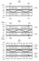
도 1은 본 발명의 일 실시예에 따른 코일 부품의 사시도이다.
도 2는 도 1의 코일 부품을 A-A'면 절단 단면도이다.
도 3은 본 발명의 다른 일 실시예에 따른 코일 부품의 절단 단면도이다.
도 4 내지 7은 도 2의 코일 부품을 제조하는 공정을 순차적으로 나타낸 도면이다.1 is a perspective view of a coil component according to an embodiment of the present invention.
Fig. 2 is a cross-sectional view taken along the line A-A 'of the coil component of Fig. 1;
3 is a cross-sectional view of a coil component according to another embodiment of the present invention.
Figs. 4 to 7 are views sequentially showing the steps of manufacturing the coil component of Fig. 2. Fig.
이하, 첨부된 도면을 참조하여 본 발명의 다양한 실시예를 상세히 설명한다. 본 실시 예들은 다른 형태로 변형되거나 여러 실시예가 서로 조합될 수 있으며, 본 발명의 범위가 이하 설명하는 실시예로 한정되는 것은 아니다. 또한, 본 실시예들은 당해 기술분야에서 평균적인 지식을 가진 자에게 본 발명을 더욱 완전하게 설명하기 위해서 제공되는 것이다. 예를 들어, 도면에서의 요소들의 형상 및 크기 등은 보다 명확한 설명을 위해 과장될 수 있다.
Hereinafter, various embodiments of the present invention will be described in detail with reference to the accompanying drawings. The embodiments may be modified in other forms or various embodiments may be combined with each other, and the scope of the present invention is not limited to the embodiments described below. Further, the embodiments are provided so that those skilled in the art can more fully understand the present invention. For example, the shape and size of the elements in the figures may be exaggerated for clarity.
한편, 본 명세서에서 사용되는 "일 실시예(one example)"라는 표현은 서로 동일한 실시예를 의미하지 않으며, 각각 서로 다른 고유한 특징을 강조하여 설명하기 위해서 제공되는 것이다. 그러나, 아래 설명에서 제시된 실시예들은 다른 실시예의 특징과 결합되어 구현되는 것을 배제하지 않는다. 예를 들어, 특정한 실시예에서 설명된 사항이 다른 실시 예에서 설명되어 있지 않더라도, 다른 실시예에서 그 사항과 반대되거나 모순되는 설명이 없는 한, 다른 실시예에 관련된 설명으로 이해될 수 있다.
The term " one example " used in this specification does not mean the same embodiment, but is provided to emphasize and describe different unique features. However, the embodiments presented in the following description do not exclude that they are implemented in combination with the features of other embodiments. For example, although the matters described in the specific embodiments are not described in the other embodiments, they may be understood as descriptions related to other embodiments unless otherwise described or contradicted by those in other embodiments.
이하에서는 본 발명의 일 실시예에 따른 코일 부품을 설명하되, 편의상 그 일 예로써 인턱터로 설명하지만, 반드시 이에 제한되는 것은 아니며, 본 발명의 내용이 다른 다양한 용도의 코일 부품에도 적용될 수 있음은 물론이다. 다른 다양한 용도의 코일 부품의 예로는, 커먼 모드 필터(Common Mode Filter), 통상의 비드(General Bead), 고주파용 비드(GHz Bead) 등을 들 수 있다.
Hereinafter, a coil component according to an embodiment of the present invention will be described as an inductor for the sake of convenience. However, the present invention is not limited thereto, and the present invention may be applied to other various coil components to be. Examples of other various uses of the coil component include a common mode filter, a general bead, and a bead for high frequency (GHz Bead).
도 1은 본 발명의 일 실시예에 따른 코일 부품의 사시도이고, 도 2는 도 1의 코일 부품을 A-A'면 절단 단면도이다. 이 경우, 도 1에 나타난 바를 기준으로 하면, 하기의 설명에서 '길이' 방향은 도 1의 'L' 방향, '폭' 방향은 'W' 방향, '두께' 방향은 'T' 방향으로 정의될 수 있다.
FIG. 1 is a perspective view of a coil component according to an embodiment of the present invention, and FIG. 2 is a cross-sectional view taken along line A-A 'of the coil component of FIG. 1, the 'length' direction is defined as the 'L' direction in FIG. 1, the 'W' direction in the 'width' direction, and the 'T' direction in the 'thickness' direction in the following description .
도 1 및 도 2를 참조하면, 본 발명의 일 실시예에 따른 코일 부품(100)은, 바디부(110), 코일부(120) 및 전극부(130)를 포함하여 구성될 수 있다.
Referring to FIGS. 1 and 2, a
바디부(110)는 코일 부품(100)의 외관을 이룬다. 바디부(110)는 길이 방향으로 마주보는 양 측면, 폭 방향으로 마주보는 양 측면, 및 두께 방향으로 마주보는 상면 및 하면으로 구성되는 대략 육면체 형상일 수 있으나, 이에 한정되는 것은 아니다.
The
바디부(110)는 자성 물질을 포함할 수 있다. 자성 물질은 자성 성질을 가지는 것이면 특별히 한정되지 않으며, 예를 들면, 순철 분말, Fe-Si계 합금 분말, Fe-Si-Al계 합금 분말, Fe-Ni계 합금 분말, Fe-Ni-Mo계 합금 분말, Fe-Ni-Mo-Cu계 합금 분말, Fe-Co계 합금 분말, Fe-Ni-Co계 합금 분말, Fe-Cr계 합금 분말, Fe-Cr-Si계 합금 분말, Fe-Ni-Cr계 합금 분말, 또는 Fe-Cr-Al계 합금 분말 등의 Fe 합금류, Fe기 비정질, Co기 비정질 등의 비정질 합금류, Mg-Zn계 페라이트, Mn-Zn계 페라이트, Mn-Mg계 페라이트, Cu-Zn계 페라이트, Mg-Mn-Sr계 페라이트, Ni-Zn계 페라이트 등의 스피넬형 페라이트류, Ba-Zn계 페라이트, Ba-Mg계 페라이트, Ba-Ni계 페라이트, Ba-Co계 페라이트, Ba-Ni-Co계 페라이트 등의 육방정형 페라이트류, Y계 페라이트 등의 가닛형 페라이트류를 들 수 있다.
The
자성 물질은 금속 자성체 분말 및 수지 혼합물을 포함하는 것일 수 있다. 금속 자성체 분말은 철(Fe), 크롬(Cr), 또는 실리콘(Si)를 주성분으로 포함할 수 있고, 예를 들면, 철(Fe)-니켈(Ni), 철(Fe), 철(Fe)-크롬(Cr)-실리콘(Si) 등을 포함할 수 있으나, 이에 한정되는 것은 아니다. 수지는 에폭시(epoxy), 폴리이미드(polyimide), 액정 결정성 폴리머(Liquid Crystal Polymer) 등을 단독 또는 혼합하여 포함할 수 있으나, 이에 한정되는 것은 아니다. 금속 자성체 분말은 2 이상의 평균 입경(D1, D2)을 갖는 금속 자성체 분말이 충진된 것일 수도 있다. 이 경우 서로 다른 크기의 바이모달(bimodal) 금속 자성체 분말를 사용하여 압착함으로써, 자성체 수지 복합체를 가득 채울 수 있어 충진율을 높일 수 있다.
The magnetic material may be one comprising a metal magnetic powder and a resin mixture. The metal magnetic material powder may include iron (Fe), chromium (Cr), or silicon (Si) as a main component. Examples of the metal magnetic powder include iron (Fe) Chromium (Cr) -silicon (Si), and the like. The resin may include, but is not limited to, epoxy, polyimide, liquid crystal polymer, etc., alone or in combination. The metal magnetic body powder may be a metal magnetic body powder having an average particle diameter (D1 , D2 ) of 2 or more. In this case, by using a bimodal metal magnetic powder of different sizes, the magnetic resin composite can be filled and the filling rate can be increased.
바디부(110)는 금속 자성체 분말 및 수지 혼합물을 포함하는 자성체 수지 복합체가 시트 형태로 성형되어 코일부(120)의 상부 및 하부에 압착 및 경화되어 형성된 것일 수 있으나, 반드시 이에 제한되는 것은 아니다. 이때, 자성체 수지 복합체의 적층 방향은 코일 부품의 실장 면에 대하여 수직할 수 있다. 여기서 수직 하다는 것은 완전한 90°뿐만 아니라 대략 90°인 경우, 즉 60~120° 정도인 것을 포함하는 개념이다.
The
전극부(130)은 코일 부품(100)이 전자 기기에 실장될 때, 코일 부품(100)을 전자 기기와 전기적으로 연결시키는 역할을 수행한다. 전극부(130)는 바디부(110) 상에 서로 이격되어 배치된 제1 및 제2 외부전극(131, 132)을 포함할 수 있다. 전극부(130)는 예를 들어, 전도성 수지층과, 전도성 수지층 상에 형성된 도체층을 포함할 수 있다. 전도성 수지층은 구리(Cu), 니켈(Ni) 및 은(Ag)으로 이루어진 군으로부터 선택된 어느 하나 이상의 도전성 금속과 열경화성 수지를 포함할 수 있다. 도체층은 니켈(Ni), 구리(Cu) 및 주석(Sn)으로 이루어진 군에서 선택된 어느 하나 이상을 포함할 수 있으며, 예를 들어, 니켈(Ni)층과 주석(Sn)층이 순차로 형성될 수 있다. 한편, 전극부(130)의 형상에 대해서는 특별히 한정하지 않으며, 예를 들어, 도 1에 도시된 바와 같이 바디부(110)의 양 측면에만 형성될 수 있고, 바디부(110)의 양 측면과 이와 연결되는 하면에 형성되어 L자 형상을 이룰 수도 있다.
The
코일부(120)는 절연층(121), 코일 도체(122) 및 봉합재(123)를 포함한다. 코일부(120)의 코어 영역(115)에는 관통 홀이 형성되어 있을 수 있으며, 이 경우, 관통 홀에는 코일 도체(122)와 동일 또는 상이한 도체 물질이 충진되어 있을 수 있다.
The
절연층(121)은 코일 형상을 가지며, 코일 부품(120)의 다른 구성요소와 코일 도체(122)를 절연시키고, 보호하는 역할을 한다. 만일 코일 도체(122)가 복수개인 경우, 이들 복수개의 코일 도체(122) 상호간을 절연시키는 역할을 수행할 수도 있다.
The
전술한 바와 같이, 기존의 박막형 인덕터에서는, 절연 기판, 예컨대, 동박 적층판(CCL, Copper Clad Laminate) 상에 코일 도체를 형성하기 때문에, 코일 부품의 전체 두께를 저감하는데 한계가 있었다. 왜냐하면, 절연 기판의 두께가 지나치게 얇아질 경우(절연 기판의 두께가 약 60μm 이하의 경우), 제조 과정에서 기판 말림이나 기판 파손 등의 불량으로 이어질 우려가 있기 때문이다. 그러나, 본 발명에서는 코일 도체가 절연 기판이 아닌 절연층 상에 배치되기 때문에, 코일부(120)의 두께를 현저히 저감할 수 있는 장점이 있으며, 이에 따라, 코일 부품(100)의 소형화 및 박형화 달성이 용이한 장점이 있다. 일 예에 따르면, 절연층(121)은 50μm 이하(0μm 제외)의 두께를 가질 수 있으며, 보다 바람직하게는 40 μm 이하(0μm 제외)의 두께를 가질 수 있으나, 반드시 이에 한정되는 것은 아니다. 한편, 절연층(121)의 두께가 얇을수록 코일 부품(100)의 소형화 및 박형화 달성에 용이한 바 그 하한에 대해서는 특별히 한정하지 않으나, 코일부에 적절한 강성을 부여하기 위한 측면에서 3μm 이상으로 할 수 있다.
As described above, in the conventional thin film type inductor, since coil conductors are formed on an insulating substrate such as a copper clad laminate (CCL), there is a limit in reducing the total thickness of the coil parts. This is because when the thickness of the insulating substrate is excessively thin (the thickness of the insulating substrate is about 60 탆 or less), there is a possibility that the substrate may be curled or the substrate may be damaged during the manufacturing process. However, in the present invention, since the coil conductor is disposed on the insulating layer, not on the insulating substrate, there is an advantage in that the thickness of the
절연층(121)의 재질은 전자의 이동을 차단하는 성질을 가진 것이라면 어느 것이든 적용될 수 있다. 예를 들면, 에폭시 수지와 같은 열경화성 수지, 폴리이미드와 같은 열가소성 수지, 또는 이들에 무기 필러와 같은 보강재가 함침된 수지, 절연 특성을 가진 고분자 등을 사용할 수 있다. 예를 들면, 시중에 상용화되고 있는 XBF, SR, PPG, PID, Perylene 등이 사용될 수 있으나, 반드시 이에 제한되는 것은 아니다.
The material of the insulating
코일 도체(122)는 절연층(121)과 대응하는 코일 형상을 가지며, 절연층(121)의 일면 및 이와 대향하는 타면 중 적어도 하나에 배치된다. 본 실시예에서는 높은 수준의 인덕턴스를 얻기 위한 측면에서 일면 및 이와 대향하는 타면 모두에 형성된 형태를 나타내었다. 즉, 절연층(121)의 일면에는 제1 코일 도체(122a)가 형성되고, 이와 대향하는 타면에는 제2 코일 도체(122b)가 형성될 수 있다. 이 경우, 제1 및 제2 코일 도체(122a, 122b)는 절연층(121)을 관통하는 비아 홀(125)을 통해 서로 연결될 수 있다.
The coil conductor 122 has a coil shape corresponding to the insulating
코일 도체(122)는 전기 전도성이 높은 금속 등의 물질로 형성될 수 있으며, 예를 들어, 은(Ag), 팔라듐(Pd), 알루미늄(Al), 니켈(Ni), 티타늄(Ti), 금(Au), 구리(Cu), 백금(Pt) 또는 이들의 합금 등으로 형성될 수 있다. 이 경우, 평면 코일 형상으로 제조하기 위한 바람직한 공정의 예로서, 전기 도금법을 이용할 수 있으며, 다만, 이와 유사한 효과를 보일 수 있는 것이라면 당 기술 분야에서 알려진 다른 공정을 이용할 수도 있을 것이다.
The coil conductor 122 may be formed of a material having high electrical conductivity such as silver, palladium (Pd), aluminum (Al), nickel (Ni), titanium (Ti) (Au), copper (Cu), platinum (Pt), an alloy thereof, or the like. In this case, electroplating may be used as an example of a preferable process for fabricating a flat coil shape, but other processes known in the art may be used as long as they can exhibit similar effects.
일 예에 따르면, 제1 및 제2 코일 도체(122a, 122b) 중 하나와 절연층(121) 사이에 형성된 시드층(123a)을 더 포함할 수 있다. 일반적으로 절연층 상에는 도금에 의한 코일 도체 형성이 어려운 바, 이를 용이하게 하기 위해 기초 금속층으로써 시드층을 형성하게 되며, 이에 모든 코일 도체는 시드층을 가지게 된다. 그러나, 후술할 바와 같이, 본 발명에서는 하나의 코일 도체는 절연층 형성에 앞서 형성하는 바, 시드층(123a)을 가지지 않는 특징을 가진다.
According to one example, the
봉합재(124)는 절연층(121) 및 코일 도체(122)를 봉합하며, 코일 부품(120)의 다른 구성요소와 이들을 절연시키고, 보호하는 역할을 한다. 봉합재(124)의 재질은 전자의 이동을 차단하는 성질을 가진 것이라면 어느 것이든 적용될 수 있다. 예를 들면, 에폭시 수지와 같은 열경화성 수지, 폴리이미드와 같은 열가소성 수지, 또는 이들에 무기 필러와 같은 보강재가 함침된 수지, 절연 특성을 가진 고분자 등을 사용할 수 있다. 예를 들면, 시중에 상용화되고 있는 XBF, SR, PPG, PID, Perylene 등이 사용될 수 있으나, 반드시 이에 제한되는 것은 아니다.
The
일 예에 따르면, 봉합재(124)는 절연층(121) 및 코일 도체(122)의 인접 패턴 사이의 공간을 충진할 수 있다. 이 경우, 바디부(110)와 코일 도체(122) 간 절연을 시킴으로써 특성 악화를 방지할 수 있을 뿐 아니라, 코일 부품의 제작 과정에서 코일 도체(122)의 변형 등의 발생을 효과적으로 방지할 수 있는 장점이 있다.
According to one example,
도 3은 본 발명의 다른 일 실시예에 따른 코일 부품의 절단 단면도이다.
3 is a cross-sectional view of a coil component according to another embodiment of the present invention.
도 3을 참조하면, 본 발명의 다른 일 실시예에 따른 코일 부품(200)은, 복수개의 절연층(221a, 221b) 및 복수개의 도체 패턴(222a, 222b, 222c)을 구비하며, 상기 복수개의 절연층(221a, 221b) 및 복수개의 도체 패턴(222a, 222b, 222c)은 서로 교대로 적층 배치된다.
3, a
도 3에는 편의상, 2개의 절연층(221a, 221b) 및 3개의 도체 패턴(222a, 222b, 222c)이 서로 교대로 적층 배치된 코일 부품(200)을 도시하였으나, 반드시 이에 제한되는 것은 아니며, 그 이상의 개수의 절연층 및 도체 패턴이 서로 교대로 적층 배치될 수도 있다고 할 것이다. 본 실시예의 경우, 인덕턴스 등 코일 특성을 보다 극대화할 수 있는 장점이 있다.
3 shows a
도 4 내지 7은 도 2의 코일 부품을 제조하는 공정을 순차적으로 나타낸 도면이다. 이하, 상술한 내용과 중복되는 설명은 생략하고, 코일 부품의 개략적인 제조 공정의 각각의 단계에 대하여 설명한다.
Figs. 4 to 7 are views sequentially showing the steps of manufacturing the coil component of Fig. 2. Fig. Hereinafter, a description overlapping with the above description will be omitted, and each step of the rough manufacturing process of the coil component will be described.
도 4를 참조하면, 먼저, 지지 부재(10)를 준비한다. 코일 부품을 제조하는 과정에서 코일부에 적절한 강성을 부여할 수 있다면 지지 부재의 구체적인 종류는 특별히 한정하지 않으나, 예를 들면, 지지 부재(10)는 동박 적층판(CCL, Copper Clad Laminate)일 수 있다. 한편, 상기 지지 부재(10)의 적어도 일면에는 금속층이 배치되어 있을 수 있으며, 이 경우, 제1 코일 도체(122a)의 형성이 용이한 장점이 있다.
Referring to FIG. 4, first, the
다음으로, 지지 부재(10)의 적어도 일면에 코일 형상의 오프닝 패턴을 갖는 제1 마스크(12)를 형성한다. 이 경우, 제1 마스크(12)는 공지의 포토리소그래피 공법을 이용하여 형성할 수 있으나, 반드시 이에 제한되는 것은 아니다. 한편, 제1 마스크(12)의 재질은 패턴 형성 후 박리가 가능하고, 빛에 의해 선택적으로 반응이 일어나는 감광성 고분자라면 어느 것이든 적용될 수 있다. 예를 들어, 제1 마스크는 네가형 포토 레지스트 혹은 포지형 포토 레지스트일 수 있다. 여기서, 네가형 포토 레지스트는 빛이 닿은 부분(노광부)의 고분자만 불용화되어 현상 후 노광부의 고분자만 잔류하게 되는 감광성 고분자로써, 이러한 네가형 포토 레지스트의 예로는, 방향족 비스아지드(bis-azide), 메타크릴산 에스테르(Methacrylic aid ester), 계피산 에스테르 등을 들 수 있으나, 반드시 이에 제한되는 것은 아니다. 한편, 포지형 포토 레지스트는 빛이 닿은 부분(노광부)의 고분자만 가용화되어 현상 후, 비노광부의 고분자만 잔류하게 되는 감광성 고분자로써, 이러한 포지형 포토 레지스트의 예로는, 폴리메타크릴산 메틸, 나프트키논디아지드, 폴리브텐-1술폰 등을 들 수 있으나, 반드시 이에 제한되는 것은 아니다.
Next, a
다음으로, 제1 마스크(12)의 오프닝 패턴에 제1 코일 도체(122a)를 형성한다. 제1 코일 도체(122a)는 당해 기술 분야에 잘 알려진 공지의 방법, 예를 들면, 드라이 필름을 이용한 무전해 도금법, 전해 도금법 등에 의해 형성할 수 있으나, 반드시 이에 제한되는 것은 아니다.
Next, the
다음으로, 제1 코일 도체(122a) 상에 절연층(121)을 형성한다. 절연층(121)은 공지의 라미네이션 공법에 의해 형성할 수 있으나, 반드시 이에 제한되는 것은 아니며, 디핑법, 기상증착법, 진공증착법 등 다양한 방식에 의해 형성할 수 있다.
Next, the insulating
도 5를 참조하면, 절연층(121)의 특정 영역에 이를 관통하는 비아을 형성한다. 비아는 추후 도체로 충진되어 비아 홀(125)을 구성하며, 이러한 비아 홀(125)은 절연층(121)의 일면 및 이에 대항하는 타면에 각각 형성된 제1 및 제2 코일 도체(122a 및 122b)을 전기적으로 연결하는 역할을 수행한다. 비아 홀(125)은 기계적 드릴/또는 레이저 드릴 등을 이용하여 형성할 수 있으나, 반드시 이에 제한되는 것은 아니며, 감광성 물질을 이용한 노광, 현상 및 박리 공정 등 다양한 방식에 희애 형성할 수 있다.
Referring to FIG. 5, a via is formed in a specific region of the insulating
다음으로, 절연층(121) 상에 시드층(123a)을 형성한다. 시드층(123a)은 후속 공정인 제2 코일 도체(122b)의 형성을 용이하게 하는 역할을 수행한다. 시드층(123a)은 스퍼터링 공법, 스핀 공법, 화학 동 공법 등을 적용하여 형성할 수 있으나, 반드시 이에 제한되는 것은 아니다.
Next, a
다음으로, 시드층(123a) 상에 코일 형상의 오프닝 패턴을 갖는 제2 마스크(13)을 형성한다. 제2 마스크(13) 역시 공지의 포토리소그래피 공법을 이용하여 형성할 수 있으나, 반드시 이에 제한되는 것은 아니다.
Next, a
도 6을 참조하면, 제2 마스크(13)의 오프닝 패턴에 제2 코일 도체(122b)를 형성한다. 제2 코일 도체(122b) 또한 당해 기술 분야에 잘 알려진 공지의 방법, 예를 들면, 드라이 필름을 이용한 무전해 도금법, 전해 도금법 등에 의해 형성할 수 있으나, 반드시 이에 제한되는 것은 아니다.
Referring to FIG. 6, a
다음으로, 제2 마스크(13)를 제거한다. 제2 마스크(13)의 제거는 당해 기술 분야에 잘 알려진 공지의 방법, 예를 들면, 박리, 에칭 등을 이용할 수 있으나, 반드시 이에 제한되는 것은 아니다.
Next, the
다음으로, 제1 코일 패턴(122a)과 지지 부재(10)를 분리한다. 만약, 지지 부재(10) 상에 금속층(11)이 배치되어 있는 경우, 제1 코일 패턴(122a)과 지지 부재(10)의 분리는, 지지 부재(10)와 그 표면에 형성된 금속층(11) 간을 분리하는 것일 수 있다.
Next, the
다음으로, 시드층(123a) 중 제2 마스크(13)에 대응하는 영역을 제거한다. 이는 당해 기술 분야에 잘 알려진 공지의 방법, 예를 들면, 에칭 등을 이용할 수 있으나, 반드시 이에 제한되는 것은 아니다. 한편, 만약 지지 부재(10) 상에 금속층(11)이 배치되어 있는 경우, 본 단계에서 금속층(11)을 함께 제거할 수 있다.
Next, a region of the
도 7을 참조하면, 제1 마스크(12) 및 절연층(121) 중 제1 마스크에 대응하는 영역을 제거한다. 이는 당해 기술 분야에 잘 알려진 공지의 방법, 예를 들면, CO2 레이저 혹은 UV 레이저에 의한 박리 등을 이용할 수 있으나, 반드시 이에 제한되는 것은 아니다.
Referring to FIG. 7, a region corresponding to the first mask of the
다음으로, 절연층(121)과 제1 및 제2 코일 도체(122a, 122b)를 봉합하는 봉합재(124)를 형성한다. 봉합재(124)의 재질은, 예를 들면, XBF, SR, PPG, PID, Perylene 등일 수 있으나, 반드시 이에 제한하지 않고 절연 특성을 지닌 타 물질로 봉합할 수 있다.
Next, a sealing
다음으로, 바디부(110)를 형성한다. 전술한 바와 같이, 바디부(110)는 시트 형태로 성형된 금속 자성체 분말 및 수지 혼합물을 포함하는 자성체 수지 복합체를 코일부(120)의 상부 및 하부에 압착 및 경화하여 형성할 수 있으나, 반드시 이에 제한되는 것은 아니다.
Next, the
한편, 본 명세서에서 제 1, 제 2 등의 표현은 한 구성요소와 다른 구성요소를 구분 짓기 위해 사용되는 것으로, 해당 구성요소들의 순서 및/또는 중요도 등을 한정하지 않는다. 경우에 따라서는 권리범위를 벗어나지 않으면서, 제 1 구성요소는 제 2 구성요소로 명명될 수도 있고, 유사하게 제 2 구성요소는 제 1 구성요소로 명명될 수도 있다.
In the present specification, the first and second expressions are used to distinguish one component from another, and do not limit the order and / or importance of the components. In some cases, without departing from the scope of the right, the first component may be referred to as a second component, and similarly, the second component may be referred to as a first component.
본 발명은 상술한 실시예 및 첨부된 도면에 의해 한정되는 것이 아니며, 첨부된 청구범위에 의해 한정하고자 한다. 따라서, 청구범위에 기재된 본 발명의 기술적 사상을 벗어나지 않는 범위 내에서 당 기술분야의 통상의 지식을 가진 자에 의해 다양한 형태의 치환, 변형 및 변경이 가능할 것이며, 이 또한 본 발명의 범위에 속한다고 할 것이다.
The present invention is not limited to the above-described embodiments and the accompanying drawings, but is intended to be limited only by the appended claims. It will be apparent to those skilled in the art that various changes in form and details may be made therein without departing from the spirit and scope of the invention as defined by the appended claims. something to do.
10: 지지 부재
11: 금속층
12, 13: 제1 및 제2 마스크
100, 200: 코일 부품
110, 210: 바디부
115, 215: 코어 영역
120, 220: 코일부
130: 전극부
131, 132: 제1 및 제2 외부 전극
121, 221a, 221b: 절연층
122a, 122b: 제1 및 제2 도체 패턴
222a, 222b, 222c: 복수의 도체 패턴
123a, 223a, 223b: 시드층
124, 224: 봉합재
125, 225a, 225b: 비아 홀10: Support member
11: metal layer
12, 13: first and second masks
100, 200: Coil parts
110, 210:
115, 215: core region
120, 220: coil part
130:
131, 132: first and second outer electrodes
121, 221a, 221b: insulating layer
122a and 122b: first and second conductor patterns
222a, 222b, 222c: a plurality of conductor patterns
123a, 223a, 223b: a seed layer
124, 224: sealing material
125, 225a, 225b: via holes
Claims (16)
Translated fromKorean상기 코일부는,
코일 형상의 절연층;
상기 절연층의 일면 및 이와 대향하는 타면 중 적어도 하나에 배치되고, 상기 절연층과 대응하는 코일 형상을 갖는 코일 도체; 및
상기 절연층 및 상기 코일 도체를 봉합하는 봉합재;를 포함하며,
상기 절연층과 상기 봉합재는 서로 독립된 공정으로 형성되어 이들 사이에는 불연속적인 계면이 형성된 코일 부품.
A coil component comprising a body part and a coil part disposed in the body part,
Wherein the coil portion includes:
A coil-shaped insulating layer;
A coil conductor disposed on at least one of the one surface of the insulating layer and the other surface facing the insulating layer, the coil conductor having a coil shape corresponding to the insulating layer; And
And a sealing material for sealing the insulating layer and the coil conductor,
Wherein the insulating layer and the sealing material are formed by processes independent of each other and a discontinuous interface is formed therebetween.
상기 봉합재는 상기 절연층 및 상기 코일 도체의 인접 패턴 사이의 공간을 충진하는 것을 특징으로 하는 코일 부품.
The method according to claim 1,
Wherein the seal material fills a space between adjacent patterns of the insulating layer and the coil conductor.
상기 코일 도체는 상기 절연층의 일면 및 타면에 각각 배치된 제1 및 제2 코일 도체를 포함하는 코일 부품.
The method according to claim 1,
Wherein the coil conductor includes first and second coil conductors disposed on one and the other sides of the insulating layer, respectively.
상기 제1 및 제2 코일 도체는 상기 절연층을 관통하는 비아 홀을 통해 서로 연결되는 코일 부품.
The method of claim 3,
Wherein the first and second coil conductors are connected to each other via via holes passing through the insulating layer.
상기 제1 및 제2 코일 도체 중 하나와 절연층 사이에 형성된 시드층을 더 포함하는 코일 부품.
The method of claim 3,
And a seed layer formed between one of said first and second coil conductors and an insulating layer.
상기 절연층 및 상기 코일 도체는 각각 복수개 구비되고, 상기 복수개의 절연층 및 코일 도체는 교대로 적층 배치되는 것을 특징으로 하는 코일 부품.
The method according to claim 1,
Wherein a plurality of the insulating layers and the coil conductors are provided, and the plurality of insulating layers and the coil conductors are alternately stacked.
상기 절연층은 40μm 이하(0μm 제외)의 두께를 갖는 코일 부품.
The method according to claim 1,
Wherein the insulating layer has a thickness of 40 탆 or less (excluding 0 탆).
상기 절연층은 페릴렌, 에폭시 및 폴리이미드로 이루어진 군으로부터 선택된 1종 이상을 포함하는 코일 부품.
The method according to claim 1,
Wherein the insulating layer comprises at least one selected from the group consisting of perylene, epoxy and polyimide.
상기 바디부는 자성 물질을 포함하는 코일 부품.
The method according to claim 1,
Wherein the body portion comprises a magnetic material.
상기 코일부의 코어 영역에는 관통 홀이 형성되고, 상기 관통 홀은 도체 물질로 충진된 코일 부품.
The method according to claim 1,
Wherein a through hole is formed in a core region of the coil portion, and the through hole is filled with a conductor material.
상기 바디부 상에 배치되고, 상기 코일 도체와 연결되는 전극부를 더 포함하는 코일 부품.
The method according to claim 1,
And an electrode portion disposed on the body portion and connected to the coil conductor.
상기 지지 부재 상에 코일 형상의 오프닝 패턴을 갖는 제1 마스크를 형성하는 단계;
상기 제1 마스크의 오프닝 패턴에 제1 코일 도체를 형성하는 단계;
상기 제1 코일 도체 상에 절연층을 형성하는 단계;
상기 제1 코일 도체와 상기 지지 부재를 분리하는 단계;
상기 제1 마스크 및 상기 절연층 중 상기 제1 마스크에 대응하는 영역을 제거하는 단계; 및
상기 절연층 및 상기 제1 코일 도체를 봉합하는 봉합재를 형성하는 단계;를 포함하며,
상기 절연층과 상기 봉합재는 서로 독립된 공정으로 형성되어 이들 사이에는 불연속적인 계면이 형성된 코일 부품의 제조방법.
Preparing a support member;
Forming a first mask having a coil-shaped opening pattern on the support member;
Forming a first coil conductor in an opening pattern of the first mask;
Forming an insulating layer on the first coil conductor;
Separating the first coil conductor and the support member;
Removing a region of the first mask and the insulating layer corresponding to the first mask; And
And forming a sealing material for sealing the insulating layer and the first coil conductor,
Wherein the insulating layer and the sealing material are formed as independent processes, and a discontinuous interface is formed therebetween.
상기 절연층 형성 후, 상기 제1 코일 도체와 상기 지지 부재를 분리하기 전,
상기 절연층 상에 시드층을 형성하는 단계;
상기 시드층 상에 코일 형상의 오프닝 패턴을 갖는 제2 마스크를 형성하는 단계;
상기 제2 마스크의 오프닝 패턴에 제2 코일 도체를 형성하는 단계;
상기 제2 마스크를 제거하는 단계;를 더 포함하고,
상기 지지 부재 분리 후,
상기 시드층 중 상기 제2 마스크에 대응하는 영역을 제거하는 단계;를 더 포함하는 코일 부품의 제조방법.
13. The method of claim 12,
After the formation of the insulating layer, before separating the first coil conductor and the support member,
Forming a seed layer on the insulating layer;
Forming a second mask having a coil-shaped opening pattern on the seed layer;
Forming a second coil conductor in an opening pattern of the second mask;
And removing the second mask,
After the support member is separated,
And removing the region of the seed layer corresponding to the second mask.
상기 지지 부재의 적어도 일면에는 금속층이 배치되고, 상기 제1 마스크는 상기 금속층 상에 형성되며,
상기 제1 코일 도체와 상기 지지 부재를 분리하는 단계는, 상기 지지 부재와 상기 금속층을 분리하는 단계인 코일 부품의 제조방법.
13. The method of claim 12,
A metal layer is disposed on at least one surface of the support member, the first mask is formed on the metal layer,
Wherein the step of separating the first coil conductor and the support member comprises separating the support member and the metal layer.
상기 지지 부재는 유리 섬유 및 절연 수지를 포함하는 코일 부품의 제조방법.
13. The method of claim 12,
Wherein the support member comprises glass fibers and an insulating resin.
상기 지지 부재의 양 면을 이용하여 2개의 코일부를 동시에 형성하는 것을 특징으로 하는 코일 부품의 제조방법.13. The method of claim 12,
Wherein the two coil parts are formed simultaneously using both surfaces of the support member.
Priority Applications (5)
| Application Number | Priority Date | Filing Date | Title |
|---|---|---|---|
| KR1020160089438AKR101832614B1 (en) | 2016-07-14 | 2016-07-14 | Coil component and method for manufactuing same |
| US15/487,987US10515754B2 (en) | 2016-07-14 | 2017-04-14 | Coil component and method of manufacturing same |
| JP2017080948AJP6361082B2 (en) | 2016-07-14 | 2017-04-14 | Coil component and manufacturing method thereof |
| CN201710406411.4ACN107622857B (en) | 2016-07-14 | 2017-06-02 | Coil assembly and method of manufacturing the same |
| US16/548,147US10566130B2 (en) | 2016-07-14 | 2019-08-22 | Coil component and method of manufacturing same |
Applications Claiming Priority (1)
| Application Number | Priority Date | Filing Date | Title |
|---|---|---|---|
| KR1020160089438AKR101832614B1 (en) | 2016-07-14 | 2016-07-14 | Coil component and method for manufactuing same |
Publications (2)
| Publication Number | Publication Date |
|---|---|
| KR20180007897A KR20180007897A (en) | 2018-01-24 |
| KR101832614B1true KR101832614B1 (en) | 2018-02-26 |
Family
ID=60941239
Family Applications (1)
| Application Number | Title | Priority Date | Filing Date |
|---|---|---|---|
| KR1020160089438AActiveKR101832614B1 (en) | 2016-07-14 | 2016-07-14 | Coil component and method for manufactuing same |
Country Status (4)
| Country | Link |
|---|---|
| US (2) | US10515754B2 (en) |
| JP (1) | JP6361082B2 (en) |
| KR (1) | KR101832614B1 (en) |
| CN (1) | CN107622857B (en) |
Cited By (1)
| Publication number | Priority date | Publication date | Assignee | Title |
|---|---|---|---|---|
| KR20210073286A (en) | 2019-12-10 | 2021-06-18 | 삼성전기주식회사 | Coil component |
Families Citing this family (10)
| Publication number | Priority date | Publication date | Assignee | Title |
|---|---|---|---|---|
| KR101862503B1 (en)* | 2017-01-06 | 2018-05-29 | 삼성전기주식회사 | Inductor and method for manufacturing the same |
| KR102080652B1 (en)* | 2018-03-14 | 2020-02-25 | 삼성전기주식회사 | Coil component |
| US10984942B2 (en) | 2018-03-14 | 2021-04-20 | Samsung Electro-Mechanics Co., Ltd. | Coil component |
| JP7553220B2 (en)* | 2018-03-20 | 2024-09-18 | 太陽誘電株式会社 | Coil parts and electronic devices |
| JP6954216B2 (en)* | 2018-04-02 | 2021-10-27 | 株式会社村田製作所 | Laminated coil parts |
| KR102064079B1 (en)* | 2018-06-04 | 2020-01-08 | 삼성전기주식회사 | Inductor |
| KR102053745B1 (en)* | 2018-07-18 | 2019-12-09 | 삼성전기주식회사 | Coil component |
| JP7056437B2 (en)* | 2018-07-25 | 2022-04-19 | 株式会社村田製作所 | Coil array parts |
| CN111524695B (en)* | 2019-02-01 | 2021-08-31 | 乾坤科技股份有限公司 | Magnetic device and method of making the same |
| KR102178528B1 (en)* | 2019-06-21 | 2020-11-13 | 삼성전기주식회사 | Coil electronic component |
Citations (2)
| Publication number | Priority date | Publication date | Assignee | Title |
|---|---|---|---|---|
| JP2004253684A (en)* | 2003-02-21 | 2004-09-09 | Tdk Corp | High density inductor and method of manufacturing the same |
| JP2016001715A (en)* | 2014-05-22 | 2016-01-07 | 新光電気工業株式会社 | Inductor, coil substrate and method for manufacturing coil substrate |
Family Cites Families (12)
| Publication number | Priority date | Publication date | Assignee | Title |
|---|---|---|---|---|
| JP3588193B2 (en)* | 1996-06-10 | 2004-11-10 | 株式会社ルネサステクノロジ | Semiconductor device and manufacturing method thereof |
| JP2005160143A (en)* | 2003-11-20 | 2005-06-16 | Toyota Motor Corp | Rotating electric machine stator |
| KR100665114B1 (en) | 2005-01-07 | 2007-01-09 | 삼성전기주식회사 | Manufacturing Method of Planar Magnetic Inductor |
| JP2007012969A (en) | 2005-07-01 | 2007-01-18 | Shinji Kudo | Laminated coil and method for manufacturing the same |
| JP2008251590A (en) | 2007-03-29 | 2008-10-16 | Matsushita Electric Ind Co Ltd | Inductance component manufacturing method |
| JP6060508B2 (en)* | 2012-03-26 | 2017-01-18 | Tdk株式会社 | Planar coil element and manufacturing method thereof |
| JP6011967B2 (en)* | 2012-10-11 | 2016-10-25 | 株式会社ケーヒン | Multilayer coil and method of manufacturing the same |
| JP5831498B2 (en)* | 2013-05-22 | 2015-12-09 | Tdk株式会社 | Coil component and manufacturing method thereof |
| KR101973410B1 (en) | 2013-08-14 | 2019-09-02 | 삼성전기주식회사 | Coil unit for thin film inductor, manufacturing method of coil unit for thin film inductor, thin film inductor and manufacturing method of thin film inductor |
| US9449753B2 (en)* | 2013-08-30 | 2016-09-20 | Qualcomm Incorporated | Varying thickness inductor |
| JP6330692B2 (en)* | 2015-02-25 | 2018-05-30 | 株式会社村田製作所 | Electronic components |
| KR102184566B1 (en)* | 2015-03-09 | 2020-12-02 | 삼성전기주식회사 | Coil electronic component and manufacturing method thereof |
- 2016
- 2016-07-14KRKR1020160089438Apatent/KR101832614B1/enactiveActive
- 2017
- 2017-04-14JPJP2017080948Apatent/JP6361082B2/enactiveActive
- 2017-04-14USUS15/487,987patent/US10515754B2/enactiveActive
- 2017-06-02CNCN201710406411.4Apatent/CN107622857B/enactiveActive
- 2019
- 2019-08-22USUS16/548,147patent/US10566130B2/enactiveActive
Patent Citations (2)
| Publication number | Priority date | Publication date | Assignee | Title |
|---|---|---|---|---|
| JP2004253684A (en)* | 2003-02-21 | 2004-09-09 | Tdk Corp | High density inductor and method of manufacturing the same |
| JP2016001715A (en)* | 2014-05-22 | 2016-01-07 | 新光電気工業株式会社 | Inductor, coil substrate and method for manufacturing coil substrate |
Cited By (2)
| Publication number | Priority date | Publication date | Assignee | Title |
|---|---|---|---|---|
| KR20210073286A (en) | 2019-12-10 | 2021-06-18 | 삼성전기주식회사 | Coil component |
| US11646146B2 (en) | 2019-12-10 | 2023-05-09 | Samsung Electro-Mechanics Co., Ltd. | Coil component |
Also Published As
| Publication number | Publication date |
|---|---|
| US10515754B2 (en) | 2019-12-24 |
| US10566130B2 (en) | 2020-02-18 |
| CN107622857A (en) | 2018-01-23 |
| JP6361082B2 (en) | 2018-07-25 |
| US20180019051A1 (en) | 2018-01-18 |
| JP2018011041A (en) | 2018-01-18 |
| KR20180007897A (en) | 2018-01-24 |
| CN107622857B (en) | 2020-03-06 |
| US20190378644A1 (en) | 2019-12-12 |
Similar Documents
| Publication | Publication Date | Title |
|---|---|---|
| KR101832614B1 (en) | Coil component and method for manufactuing same | |
| JP6562363B2 (en) | Multilayer conductive pattern inductor and manufacturing method thereof | |
| KR101659216B1 (en) | Coil electronic component and manufacturing method thereof | |
| KR101832608B1 (en) | Coil electronic part and manufacturing method thereof | |
| JP4404088B2 (en) | Coil parts | |
| JP5874199B2 (en) | Coil component and manufacturing method thereof | |
| KR101762039B1 (en) | Coil component | |
| CN108573791B (en) | Coil electronic component and method for manufacturing same | |
| KR101503144B1 (en) | Thin film type inductor and method of manufacturing the same | |
| KR102016490B1 (en) | Coil Component | |
| JP7223525B2 (en) | Inductor and inductor manufacturing method | |
| JP6460220B1 (en) | Coil component and manufacturing method thereof | |
| KR101963287B1 (en) | Coil component and method for manufacturing the same | |
| KR20180133153A (en) | Coil component and method for manufacturing the same | |
| US10636562B2 (en) | Coil electronic component and method of manufacturing the same | |
| US10395814B2 (en) | Coil electronic component and method of manufacturing the same | |
| US11017936B2 (en) | Coil electronic component | |
| US10515753B2 (en) | Coil component and method of manufacturing the same | |
| JP2000049013A (en) | Electronic components | |
| US20250022641A1 (en) | Electronic component and method for manufacturing the same |
Legal Events
| Date | Code | Title | Description |
|---|---|---|---|
| A201 | Request for examination | ||
| PA0109 | Patent application | Patent event code:PA01091R01D Comment text:Patent Application Patent event date:20160714 | |
| PA0201 | Request for examination | ||
| E902 | Notification of reason for refusal | ||
| PE0902 | Notice of grounds for rejection | Comment text:Notification of reason for refusal Patent event date:20170720 Patent event code:PE09021S01D | |
| E701 | Decision to grant or registration of patent right | ||
| PE0701 | Decision of registration | Patent event code:PE07011S01D Comment text:Decision to Grant Registration Patent event date:20171229 | |
| PG1501 | Laying open of application | ||
| GRNT | Written decision to grant | ||
| PR0701 | Registration of establishment | Comment text:Registration of Establishment Patent event date:20180220 Patent event code:PR07011E01D | |
| PR1002 | Payment of registration fee | Payment date:20180220 End annual number:3 Start annual number:1 | |
| PG1601 | Publication of registration | ||
| PR1001 | Payment of annual fee | Payment date:20210104 Start annual number:4 End annual number:4 | |
| PR1001 | Payment of annual fee | Payment date:20211221 Start annual number:5 End annual number:5 | |
| PR1001 | Payment of annual fee | Payment date:20221226 Start annual number:6 End annual number:6 | |
| PR1001 | Payment of annual fee | Payment date:20250124 Start annual number:8 End annual number:8 |