KR101830904B1 - Recessed semiconductor substrates - Google Patents
Recessed semiconductor substratesDownload PDFInfo
- Publication number
- KR101830904B1 KR101830904B1KR1020127015804AKR20127015804AKR101830904B1KR 101830904 B1KR101830904 B1KR 101830904B1KR 1020127015804 AKR1020127015804 AKR 1020127015804AKR 20127015804 AKR20127015804 AKR 20127015804AKR 101830904 B1KR101830904 B1KR 101830904B1
- Authority
- KR
- South Korea
- Prior art keywords
- semiconductor substrate
- vias
- die
- recessed
- coupled
- Prior art date
- Legal status (The legal status is an assumption and is not a legal conclusion. Google has not performed a legal analysis and makes no representation as to the accuracy of the status listed.)
- Active
Links
Images


Classifications
- H—ELECTRICITY
- H01—ELECTRIC ELEMENTS
- H01L—SEMICONDUCTOR DEVICES NOT COVERED BY CLASS H10
- H01L25/00—Assemblies consisting of a plurality of semiconductor or other solid state devices
- H01L25/03—Assemblies consisting of a plurality of semiconductor or other solid state devices all the devices being of a type provided for in a single subclass of subclasses H10B, H10D, H10F, H10H, H10K or H10N, e.g. assemblies of rectifier diodes
- H01L25/04—Assemblies consisting of a plurality of semiconductor or other solid state devices all the devices being of a type provided for in a single subclass of subclasses H10B, H10D, H10F, H10H, H10K or H10N, e.g. assemblies of rectifier diodes the devices not having separate containers
- H—ELECTRICITY
- H01—ELECTRIC ELEMENTS
- H01L—SEMICONDUCTOR DEVICES NOT COVERED BY CLASS H10
- H01L23/00—Details of semiconductor or other solid state devices
- H01L23/12—Mountings, e.g. non-detachable insulating substrates
- H01L23/13—Mountings, e.g. non-detachable insulating substrates characterised by the shape
- H—ELECTRICITY
- H01—ELECTRIC ELEMENTS
- H01L—SEMICONDUCTOR DEVICES NOT COVERED BY CLASS H10
- H01L21/00—Processes or apparatus adapted for the manufacture or treatment of semiconductor or solid state devices or of parts thereof
- H01L21/02—Manufacture or treatment of semiconductor devices or of parts thereof
- H01L21/04—Manufacture or treatment of semiconductor devices or of parts thereof the devices having potential barriers, e.g. a PN junction, depletion layer or carrier concentration layer
- H01L21/48—Manufacture or treatment of parts, e.g. containers, prior to assembly of the devices, using processes not provided for in a single one of the groups H01L21/18 - H01L21/326 or H10D48/04 - H10D48/07
- H01L21/4814—Conductive parts
- H01L21/4846—Leads on or in insulating or insulated substrates, e.g. metallisation
- H01L21/486—Via connections through the substrate with or without pins
- H—ELECTRICITY
- H01—ELECTRIC ELEMENTS
- H01L—SEMICONDUCTOR DEVICES NOT COVERED BY CLASS H10
- H01L21/00—Processes or apparatus adapted for the manufacture or treatment of semiconductor or solid state devices or of parts thereof
- H01L21/02—Manufacture or treatment of semiconductor devices or of parts thereof
- H01L21/04—Manufacture or treatment of semiconductor devices or of parts thereof the devices having potential barriers, e.g. a PN junction, depletion layer or carrier concentration layer
- H01L21/50—Assembly of semiconductor devices using processes or apparatus not provided for in a single one of the groups H01L21/18 - H01L21/326 or H10D48/04 - H10D48/07 e.g. sealing of a cap to a base of a container
- H01L21/56—Encapsulations, e.g. encapsulation layers, coatings
- H01L21/565—Moulds
- H—ELECTRICITY
- H01—ELECTRIC ELEMENTS
- H01L—SEMICONDUCTOR DEVICES NOT COVERED BY CLASS H10
- H01L21/00—Processes or apparatus adapted for the manufacture or treatment of semiconductor or solid state devices or of parts thereof
- H01L21/70—Manufacture or treatment of devices consisting of a plurality of solid state components formed in or on a common substrate or of parts thereof; Manufacture of integrated circuit devices or of parts thereof
- H01L21/71—Manufacture of specific parts of devices defined in group H01L21/70
- H01L21/768—Applying interconnections to be used for carrying current between separate components within a device comprising conductors and dielectrics
- H01L21/76838—Applying interconnections to be used for carrying current between separate components within a device comprising conductors and dielectrics characterised by the formation and the after-treatment of the conductors
- H01L21/76877—Filling of holes, grooves or trenches, e.g. vias, with conductive material
- H—ELECTRICITY
- H01—ELECTRIC ELEMENTS
- H01L—SEMICONDUCTOR DEVICES NOT COVERED BY CLASS H10
- H01L21/00—Processes or apparatus adapted for the manufacture or treatment of semiconductor or solid state devices or of parts thereof
- H01L21/70—Manufacture or treatment of devices consisting of a plurality of solid state components formed in or on a common substrate or of parts thereof; Manufacture of integrated circuit devices or of parts thereof
- H01L21/71—Manufacture of specific parts of devices defined in group H01L21/70
- H01L21/768—Applying interconnections to be used for carrying current between separate components within a device comprising conductors and dielectrics
- H01L21/76898—Applying interconnections to be used for carrying current between separate components within a device comprising conductors and dielectrics formed through a semiconductor substrate
- H—ELECTRICITY
- H01—ELECTRIC ELEMENTS
- H01L—SEMICONDUCTOR DEVICES NOT COVERED BY CLASS H10
- H01L23/00—Details of semiconductor or other solid state devices
- H01L23/12—Mountings, e.g. non-detachable insulating substrates
- H01L23/14—Mountings, e.g. non-detachable insulating substrates characterised by the material or its electrical properties
- H01L23/147—Semiconductor insulating substrates
- H—ELECTRICITY
- H01—ELECTRIC ELEMENTS
- H01L—SEMICONDUCTOR DEVICES NOT COVERED BY CLASS H10
- H01L23/00—Details of semiconductor or other solid state devices
- H01L23/48—Arrangements for conducting electric current to or from the solid state body in operation, e.g. leads, terminal arrangements ; Selection of materials therefor
- H01L23/488—Arrangements for conducting electric current to or from the solid state body in operation, e.g. leads, terminal arrangements ; Selection of materials therefor consisting of soldered or bonded constructions
- H01L23/498—Leads, i.e. metallisations or lead-frames on insulating substrates, e.g. chip carriers
- H01L23/49827—Via connections through the substrates, e.g. pins going through the substrate, coaxial cables
- H—ELECTRICITY
- H01—ELECTRIC ELEMENTS
- H01L—SEMICONDUCTOR DEVICES NOT COVERED BY CLASS H10
- H01L23/00—Details of semiconductor or other solid state devices
- H01L23/48—Arrangements for conducting electric current to or from the solid state body in operation, e.g. leads, terminal arrangements ; Selection of materials therefor
- H01L23/488—Arrangements for conducting electric current to or from the solid state body in operation, e.g. leads, terminal arrangements ; Selection of materials therefor consisting of soldered or bonded constructions
- H01L23/498—Leads, i.e. metallisations or lead-frames on insulating substrates, e.g. chip carriers
- H01L23/49833—Leads, i.e. metallisations or lead-frames on insulating substrates, e.g. chip carriers the chip support structure consisting of a plurality of insulating substrates
- H—ELECTRICITY
- H01—ELECTRIC ELEMENTS
- H01L—SEMICONDUCTOR DEVICES NOT COVERED BY CLASS H10
- H01L23/00—Details of semiconductor or other solid state devices
- H01L23/48—Arrangements for conducting electric current to or from the solid state body in operation, e.g. leads, terminal arrangements ; Selection of materials therefor
- H01L23/488—Arrangements for conducting electric current to or from the solid state body in operation, e.g. leads, terminal arrangements ; Selection of materials therefor consisting of soldered or bonded constructions
- H01L23/498—Leads, i.e. metallisations or lead-frames on insulating substrates, e.g. chip carriers
- H01L23/49838—Geometry or layout
- H—ELECTRICITY
- H01—ELECTRIC ELEMENTS
- H01L—SEMICONDUCTOR DEVICES NOT COVERED BY CLASS H10
- H01L24/00—Arrangements for connecting or disconnecting semiconductor or solid-state bodies; Methods or apparatus related thereto
- H01L24/01—Means for bonding being attached to, or being formed on, the surface to be connected, e.g. chip-to-package, die-attach, "first-level" interconnects; Manufacturing methods related thereto
- H01L24/02—Bonding areas ; Manufacturing methods related thereto
- H01L24/07—Structure, shape, material or disposition of the bonding areas after the connecting process
- H01L24/09—Structure, shape, material or disposition of the bonding areas after the connecting process of a plurality of bonding areas
- H—ELECTRICITY
- H01—ELECTRIC ELEMENTS
- H01L—SEMICONDUCTOR DEVICES NOT COVERED BY CLASS H10
- H01L24/00—Arrangements for connecting or disconnecting semiconductor or solid-state bodies; Methods or apparatus related thereto
- H01L24/01—Means for bonding being attached to, or being formed on, the surface to be connected, e.g. chip-to-package, die-attach, "first-level" interconnects; Manufacturing methods related thereto
- H01L24/10—Bump connectors ; Manufacturing methods related thereto
- H01L24/15—Structure, shape, material or disposition of the bump connectors after the connecting process
- H01L24/17—Structure, shape, material or disposition of the bump connectors after the connecting process of a plurality of bump connectors
- H—ELECTRICITY
- H01—ELECTRIC ELEMENTS
- H01L—SEMICONDUCTOR DEVICES NOT COVERED BY CLASS H10
- H01L24/00—Arrangements for connecting or disconnecting semiconductor or solid-state bodies; Methods or apparatus related thereto
- H01L24/01—Means for bonding being attached to, or being formed on, the surface to be connected, e.g. chip-to-package, die-attach, "first-level" interconnects; Manufacturing methods related thereto
- H01L24/26—Layer connectors, e.g. plate connectors, solder or adhesive layers; Manufacturing methods related thereto
- H01L24/31—Structure, shape, material or disposition of the layer connectors after the connecting process
- H01L24/33—Structure, shape, material or disposition of the layer connectors after the connecting process of a plurality of layer connectors
- H—ELECTRICITY
- H01—ELECTRIC ELEMENTS
- H01L—SEMICONDUCTOR DEVICES NOT COVERED BY CLASS H10
- H01L24/00—Arrangements for connecting or disconnecting semiconductor or solid-state bodies; Methods or apparatus related thereto
- H01L24/80—Methods for connecting semiconductor or other solid state bodies using means for bonding being attached to, or being formed on, the surface to be connected
- H01L24/81—Methods for connecting semiconductor or other solid state bodies using means for bonding being attached to, or being formed on, the surface to be connected using a bump connector
- H—ELECTRICITY
- H01—ELECTRIC ELEMENTS
- H01L—SEMICONDUCTOR DEVICES NOT COVERED BY CLASS H10
- H01L25/00—Assemblies consisting of a plurality of semiconductor or other solid state devices
- H01L25/03—Assemblies consisting of a plurality of semiconductor or other solid state devices all the devices being of a type provided for in a single subclass of subclasses H10B, H10D, H10F, H10H, H10K or H10N, e.g. assemblies of rectifier diodes
- H01L25/04—Assemblies consisting of a plurality of semiconductor or other solid state devices all the devices being of a type provided for in a single subclass of subclasses H10B, H10D, H10F, H10H, H10K or H10N, e.g. assemblies of rectifier diodes the devices not having separate containers
- H01L25/065—Assemblies consisting of a plurality of semiconductor or other solid state devices all the devices being of a type provided for in a single subclass of subclasses H10B, H10D, H10F, H10H, H10K or H10N, e.g. assemblies of rectifier diodes the devices not having separate containers the devices being of a type provided for in group H10D89/00
- H01L25/0652—Assemblies consisting of a plurality of semiconductor or other solid state devices all the devices being of a type provided for in a single subclass of subclasses H10B, H10D, H10F, H10H, H10K or H10N, e.g. assemblies of rectifier diodes the devices not having separate containers the devices being of a type provided for in group H10D89/00 the devices being arranged next and on each other, i.e. mixed assemblies
- H—ELECTRICITY
- H01—ELECTRIC ELEMENTS
- H01L—SEMICONDUCTOR DEVICES NOT COVERED BY CLASS H10
- H01L25/00—Assemblies consisting of a plurality of semiconductor or other solid state devices
- H01L25/03—Assemblies consisting of a plurality of semiconductor or other solid state devices all the devices being of a type provided for in a single subclass of subclasses H10B, H10D, H10F, H10H, H10K or H10N, e.g. assemblies of rectifier diodes
- H01L25/04—Assemblies consisting of a plurality of semiconductor or other solid state devices all the devices being of a type provided for in a single subclass of subclasses H10B, H10D, H10F, H10H, H10K or H10N, e.g. assemblies of rectifier diodes the devices not having separate containers
- H01L25/065—Assemblies consisting of a plurality of semiconductor or other solid state devices all the devices being of a type provided for in a single subclass of subclasses H10B, H10D, H10F, H10H, H10K or H10N, e.g. assemblies of rectifier diodes the devices not having separate containers the devices being of a type provided for in group H10D89/00
- H01L25/0655—Assemblies consisting of a plurality of semiconductor or other solid state devices all the devices being of a type provided for in a single subclass of subclasses H10B, H10D, H10F, H10H, H10K or H10N, e.g. assemblies of rectifier diodes the devices not having separate containers the devices being of a type provided for in group H10D89/00 the devices being arranged next to each other
- H—ELECTRICITY
- H01—ELECTRIC ELEMENTS
- H01L—SEMICONDUCTOR DEVICES NOT COVERED BY CLASS H10
- H01L25/00—Assemblies consisting of a plurality of semiconductor or other solid state devices
- H01L25/03—Assemblies consisting of a plurality of semiconductor or other solid state devices all the devices being of a type provided for in a single subclass of subclasses H10B, H10D, H10F, H10H, H10K or H10N, e.g. assemblies of rectifier diodes
- H01L25/04—Assemblies consisting of a plurality of semiconductor or other solid state devices all the devices being of a type provided for in a single subclass of subclasses H10B, H10D, H10F, H10H, H10K or H10N, e.g. assemblies of rectifier diodes the devices not having separate containers
- H01L25/065—Assemblies consisting of a plurality of semiconductor or other solid state devices all the devices being of a type provided for in a single subclass of subclasses H10B, H10D, H10F, H10H, H10K or H10N, e.g. assemblies of rectifier diodes the devices not having separate containers the devices being of a type provided for in group H10D89/00
- H01L25/0657—Stacked arrangements of devices
- H—ELECTRICITY
- H01—ELECTRIC ELEMENTS
- H01L—SEMICONDUCTOR DEVICES NOT COVERED BY CLASS H10
- H01L25/00—Assemblies consisting of a plurality of semiconductor or other solid state devices
- H01L25/03—Assemblies consisting of a plurality of semiconductor or other solid state devices all the devices being of a type provided for in a single subclass of subclasses H10B, H10D, H10F, H10H, H10K or H10N, e.g. assemblies of rectifier diodes
- H01L25/10—Assemblies consisting of a plurality of semiconductor or other solid state devices all the devices being of a type provided for in a single subclass of subclasses H10B, H10D, H10F, H10H, H10K or H10N, e.g. assemblies of rectifier diodes the devices having separate containers
- H01L25/105—Assemblies consisting of a plurality of semiconductor or other solid state devices all the devices being of a type provided for in a single subclass of subclasses H10B, H10D, H10F, H10H, H10K or H10N, e.g. assemblies of rectifier diodes the devices having separate containers the devices being integrated devices of class H10
- H—ELECTRICITY
- H01—ELECTRIC ELEMENTS
- H01L—SEMICONDUCTOR DEVICES NOT COVERED BY CLASS H10
- H01L25/00—Assemblies consisting of a plurality of semiconductor or other solid state devices
- H01L25/50—Multistep manufacturing processes of assemblies consisting of devices, the devices being individual devices of subclass H10D or integrated devices of class H10
- H—ELECTRICITY
- H01—ELECTRIC ELEMENTS
- H01L—SEMICONDUCTOR DEVICES NOT COVERED BY CLASS H10
- H01L2224/00—Indexing scheme for arrangements for connecting or disconnecting semiconductor or solid-state bodies and methods related thereto as covered by H01L24/00
- H01L2224/01—Means for bonding being attached to, or being formed on, the surface to be connected, e.g. chip-to-package, die-attach, "first-level" interconnects; Manufacturing methods related thereto
- H01L2224/02—Bonding areas; Manufacturing methods related thereto
- H01L2224/023—Redistribution layers [RDL] for bonding areas
- H01L2224/0237—Disposition of the redistribution layers
- H01L2224/02372—Disposition of the redistribution layers connecting to a via connection in the semiconductor or solid-state body
- H—ELECTRICITY
- H01—ELECTRIC ELEMENTS
- H01L—SEMICONDUCTOR DEVICES NOT COVERED BY CLASS H10
- H01L2224/00—Indexing scheme for arrangements for connecting or disconnecting semiconductor or solid-state bodies and methods related thereto as covered by H01L24/00
- H01L2224/01—Means for bonding being attached to, or being formed on, the surface to be connected, e.g. chip-to-package, die-attach, "first-level" interconnects; Manufacturing methods related thereto
- H01L2224/02—Bonding areas; Manufacturing methods related thereto
- H01L2224/04—Structure, shape, material or disposition of the bonding areas prior to the connecting process
- H01L2224/0401—Bonding areas specifically adapted for bump connectors, e.g. under bump metallisation [UBM]
- H—ELECTRICITY
- H01—ELECTRIC ELEMENTS
- H01L—SEMICONDUCTOR DEVICES NOT COVERED BY CLASS H10
- H01L2224/00—Indexing scheme for arrangements for connecting or disconnecting semiconductor or solid-state bodies and methods related thereto as covered by H01L24/00
- H01L2224/01—Means for bonding being attached to, or being formed on, the surface to be connected, e.g. chip-to-package, die-attach, "first-level" interconnects; Manufacturing methods related thereto
- H01L2224/02—Bonding areas; Manufacturing methods related thereto
- H01L2224/04—Structure, shape, material or disposition of the bonding areas prior to the connecting process
- H01L2224/05—Structure, shape, material or disposition of the bonding areas prior to the connecting process of an individual bonding area
- H01L2224/0554—External layer
- H01L2224/05599—Material
- H01L2224/056—Material with a principal constituent of the material being a metal or a metalloid, e.g. boron [B], silicon [Si], germanium [Ge], arsenic [As], antimony [Sb], tellurium [Te] and polonium [Po], and alloys thereof
- H01L2224/05617—Material with a principal constituent of the material being a metal or a metalloid, e.g. boron [B], silicon [Si], germanium [Ge], arsenic [As], antimony [Sb], tellurium [Te] and polonium [Po], and alloys thereof the principal constituent melting at a temperature of greater than or equal to 400°C and less than 950°C
- H01L2224/05624—Aluminium [Al] as principal constituent
- H—ELECTRICITY
- H01—ELECTRIC ELEMENTS
- H01L—SEMICONDUCTOR DEVICES NOT COVERED BY CLASS H10
- H01L2224/00—Indexing scheme for arrangements for connecting or disconnecting semiconductor or solid-state bodies and methods related thereto as covered by H01L24/00
- H01L2224/01—Means for bonding being attached to, or being formed on, the surface to be connected, e.g. chip-to-package, die-attach, "first-level" interconnects; Manufacturing methods related thereto
- H01L2224/02—Bonding areas; Manufacturing methods related thereto
- H01L2224/04—Structure, shape, material or disposition of the bonding areas prior to the connecting process
- H01L2224/05—Structure, shape, material or disposition of the bonding areas prior to the connecting process of an individual bonding area
- H01L2224/0554—External layer
- H01L2224/05599—Material
- H01L2224/056—Material with a principal constituent of the material being a metal or a metalloid, e.g. boron [B], silicon [Si], germanium [Ge], arsenic [As], antimony [Sb], tellurium [Te] and polonium [Po], and alloys thereof
- H01L2224/05638—Material with a principal constituent of the material being a metal or a metalloid, e.g. boron [B], silicon [Si], germanium [Ge], arsenic [As], antimony [Sb], tellurium [Te] and polonium [Po], and alloys thereof the principal constituent melting at a temperature of greater than or equal to 950°C and less than 1550°C
- H01L2224/05647—Copper [Cu] as principal constituent
- H—ELECTRICITY
- H01—ELECTRIC ELEMENTS
- H01L—SEMICONDUCTOR DEVICES NOT COVERED BY CLASS H10
- H01L2224/00—Indexing scheme for arrangements for connecting or disconnecting semiconductor or solid-state bodies and methods related thereto as covered by H01L24/00
- H01L2224/01—Means for bonding being attached to, or being formed on, the surface to be connected, e.g. chip-to-package, die-attach, "first-level" interconnects; Manufacturing methods related thereto
- H01L2224/10—Bump connectors; Manufacturing methods related thereto
- H01L2224/12—Structure, shape, material or disposition of the bump connectors prior to the connecting process
- H01L2224/13—Structure, shape, material or disposition of the bump connectors prior to the connecting process of an individual bump connector
- H01L2224/13001—Core members of the bump connector
- H01L2224/1302—Disposition
- H01L2224/13024—Disposition the bump connector being disposed on a redistribution layer on the semiconductor or solid-state body
- H—ELECTRICITY
- H01—ELECTRIC ELEMENTS
- H01L—SEMICONDUCTOR DEVICES NOT COVERED BY CLASS H10
- H01L2224/00—Indexing scheme for arrangements for connecting or disconnecting semiconductor or solid-state bodies and methods related thereto as covered by H01L24/00
- H01L2224/01—Means for bonding being attached to, or being formed on, the surface to be connected, e.g. chip-to-package, die-attach, "first-level" interconnects; Manufacturing methods related thereto
- H01L2224/10—Bump connectors; Manufacturing methods related thereto
- H01L2224/12—Structure, shape, material or disposition of the bump connectors prior to the connecting process
- H01L2224/13—Structure, shape, material or disposition of the bump connectors prior to the connecting process of an individual bump connector
- H01L2224/13001—Core members of the bump connector
- H01L2224/1302—Disposition
- H01L2224/13025—Disposition the bump connector being disposed on a via connection of the semiconductor or solid-state body
- H—ELECTRICITY
- H01—ELECTRIC ELEMENTS
- H01L—SEMICONDUCTOR DEVICES NOT COVERED BY CLASS H10
- H01L2224/00—Indexing scheme for arrangements for connecting or disconnecting semiconductor or solid-state bodies and methods related thereto as covered by H01L24/00
- H01L2224/01—Means for bonding being attached to, or being formed on, the surface to be connected, e.g. chip-to-package, die-attach, "first-level" interconnects; Manufacturing methods related thereto
- H01L2224/10—Bump connectors; Manufacturing methods related thereto
- H01L2224/12—Structure, shape, material or disposition of the bump connectors prior to the connecting process
- H01L2224/14—Structure, shape, material or disposition of the bump connectors prior to the connecting process of a plurality of bump connectors
- H01L2224/141—Disposition
- H01L2224/1418—Disposition being disposed on at least two different sides of the body, e.g. dual array
- H01L2224/14181—On opposite sides of the body
- H—ELECTRICITY
- H01—ELECTRIC ELEMENTS
- H01L—SEMICONDUCTOR DEVICES NOT COVERED BY CLASS H10
- H01L2224/00—Indexing scheme for arrangements for connecting or disconnecting semiconductor or solid-state bodies and methods related thereto as covered by H01L24/00
- H01L2224/01—Means for bonding being attached to, or being formed on, the surface to be connected, e.g. chip-to-package, die-attach, "first-level" interconnects; Manufacturing methods related thereto
- H01L2224/10—Bump connectors; Manufacturing methods related thereto
- H01L2224/15—Structure, shape, material or disposition of the bump connectors after the connecting process
- H01L2224/16—Structure, shape, material or disposition of the bump connectors after the connecting process of an individual bump connector
- H01L2224/161—Disposition
- H01L2224/16151—Disposition the bump connector connecting between a semiconductor or solid-state body and an item not being a semiconductor or solid-state body, e.g. chip-to-substrate, chip-to-passive
- H01L2224/16221—Disposition the bump connector connecting between a semiconductor or solid-state body and an item not being a semiconductor or solid-state body, e.g. chip-to-substrate, chip-to-passive the body and the item being stacked
- H01L2224/16225—Disposition the bump connector connecting between a semiconductor or solid-state body and an item not being a semiconductor or solid-state body, e.g. chip-to-substrate, chip-to-passive the body and the item being stacked the item being non-metallic, e.g. insulating substrate with or without metallisation
- H01L2224/16235—Disposition the bump connector connecting between a semiconductor or solid-state body and an item not being a semiconductor or solid-state body, e.g. chip-to-substrate, chip-to-passive the body and the item being stacked the item being non-metallic, e.g. insulating substrate with or without metallisation the bump connector connecting to a via metallisation of the item
- H—ELECTRICITY
- H01—ELECTRIC ELEMENTS
- H01L—SEMICONDUCTOR DEVICES NOT COVERED BY CLASS H10
- H01L2224/00—Indexing scheme for arrangements for connecting or disconnecting semiconductor or solid-state bodies and methods related thereto as covered by H01L24/00
- H01L2224/01—Means for bonding being attached to, or being formed on, the surface to be connected, e.g. chip-to-package, die-attach, "first-level" interconnects; Manufacturing methods related thereto
- H01L2224/10—Bump connectors; Manufacturing methods related thereto
- H01L2224/15—Structure, shape, material or disposition of the bump connectors after the connecting process
- H01L2224/16—Structure, shape, material or disposition of the bump connectors after the connecting process of an individual bump connector
- H01L2224/161—Disposition
- H01L2224/16151—Disposition the bump connector connecting between a semiconductor or solid-state body and an item not being a semiconductor or solid-state body, e.g. chip-to-substrate, chip-to-passive
- H01L2224/16221—Disposition the bump connector connecting between a semiconductor or solid-state body and an item not being a semiconductor or solid-state body, e.g. chip-to-substrate, chip-to-passive the body and the item being stacked
- H01L2224/16225—Disposition the bump connector connecting between a semiconductor or solid-state body and an item not being a semiconductor or solid-state body, e.g. chip-to-substrate, chip-to-passive the body and the item being stacked the item being non-metallic, e.g. insulating substrate with or without metallisation
- H01L2224/16238—Disposition the bump connector connecting between a semiconductor or solid-state body and an item not being a semiconductor or solid-state body, e.g. chip-to-substrate, chip-to-passive the body and the item being stacked the item being non-metallic, e.g. insulating substrate with or without metallisation the bump connector connecting to a bonding area protruding from the surface of the item
- H—ELECTRICITY
- H01—ELECTRIC ELEMENTS
- H01L—SEMICONDUCTOR DEVICES NOT COVERED BY CLASS H10
- H01L2224/00—Indexing scheme for arrangements for connecting or disconnecting semiconductor or solid-state bodies and methods related thereto as covered by H01L24/00
- H01L2224/01—Means for bonding being attached to, or being formed on, the surface to be connected, e.g. chip-to-package, die-attach, "first-level" interconnects; Manufacturing methods related thereto
- H01L2224/26—Layer connectors, e.g. plate connectors, solder or adhesive layers; Manufacturing methods related thereto
- H01L2224/31—Structure, shape, material or disposition of the layer connectors after the connecting process
- H01L2224/32—Structure, shape, material or disposition of the layer connectors after the connecting process of an individual layer connector
- H01L2224/321—Disposition
- H01L2224/32151—Disposition the layer connector connecting between a semiconductor or solid-state body and an item not being a semiconductor or solid-state body, e.g. chip-to-substrate, chip-to-passive
- H01L2224/32221—Disposition the layer connector connecting between a semiconductor or solid-state body and an item not being a semiconductor or solid-state body, e.g. chip-to-substrate, chip-to-passive the body and the item being stacked
- H01L2224/32225—Disposition the layer connector connecting between a semiconductor or solid-state body and an item not being a semiconductor or solid-state body, e.g. chip-to-substrate, chip-to-passive the body and the item being stacked the item being non-metallic, e.g. insulating substrate with or without metallisation
- H—ELECTRICITY
- H01—ELECTRIC ELEMENTS
- H01L—SEMICONDUCTOR DEVICES NOT COVERED BY CLASS H10
- H01L2224/00—Indexing scheme for arrangements for connecting or disconnecting semiconductor or solid-state bodies and methods related thereto as covered by H01L24/00
- H01L2224/01—Means for bonding being attached to, or being formed on, the surface to be connected, e.g. chip-to-package, die-attach, "first-level" interconnects; Manufacturing methods related thereto
- H01L2224/42—Wire connectors; Manufacturing methods related thereto
- H01L2224/47—Structure, shape, material or disposition of the wire connectors after the connecting process
- H01L2224/48—Structure, shape, material or disposition of the wire connectors after the connecting process of an individual wire connector
- H01L2224/481—Disposition
- H01L2224/48151—Connecting between a semiconductor or solid-state body and an item not being a semiconductor or solid-state body, e.g. chip-to-substrate, chip-to-passive
- H01L2224/48221—Connecting between a semiconductor or solid-state body and an item not being a semiconductor or solid-state body, e.g. chip-to-substrate, chip-to-passive the body and the item being stacked
- H01L2224/48225—Connecting between a semiconductor or solid-state body and an item not being a semiconductor or solid-state body, e.g. chip-to-substrate, chip-to-passive the body and the item being stacked the item being non-metallic, e.g. insulating substrate with or without metallisation
- H01L2224/48227—Connecting between a semiconductor or solid-state body and an item not being a semiconductor or solid-state body, e.g. chip-to-substrate, chip-to-passive the body and the item being stacked the item being non-metallic, e.g. insulating substrate with or without metallisation connecting the wire to a bond pad of the item
- H—ELECTRICITY
- H01—ELECTRIC ELEMENTS
- H01L—SEMICONDUCTOR DEVICES NOT COVERED BY CLASS H10
- H01L2224/00—Indexing scheme for arrangements for connecting or disconnecting semiconductor or solid-state bodies and methods related thereto as covered by H01L24/00
- H01L2224/73—Means for bonding being of different types provided for in two or more of groups H01L2224/10, H01L2224/18, H01L2224/26, H01L2224/34, H01L2224/42, H01L2224/50, H01L2224/63, H01L2224/71
- H01L2224/732—Location after the connecting process
- H01L2224/73251—Location after the connecting process on different surfaces
- H01L2224/73265—Layer and wire connectors
- H—ELECTRICITY
- H01—ELECTRIC ELEMENTS
- H01L—SEMICONDUCTOR DEVICES NOT COVERED BY CLASS H10
- H01L2224/00—Indexing scheme for arrangements for connecting or disconnecting semiconductor or solid-state bodies and methods related thereto as covered by H01L24/00
- H01L2224/80—Methods for connecting semiconductor or other solid state bodies using means for bonding being attached to, or being formed on, the surface to be connected
- H01L2224/81—Methods for connecting semiconductor or other solid state bodies using means for bonding being attached to, or being formed on, the surface to be connected using a bump connector
- H01L2224/8119—Arrangement of the bump connectors prior to mounting
- H01L2224/81193—Arrangement of the bump connectors prior to mounting wherein the bump connectors are disposed on both the semiconductor or solid-state body and another item or body to be connected to the semiconductor or solid-state body
- H—ELECTRICITY
- H01—ELECTRIC ELEMENTS
- H01L—SEMICONDUCTOR DEVICES NOT COVERED BY CLASS H10
- H01L2224/00—Indexing scheme for arrangements for connecting or disconnecting semiconductor or solid-state bodies and methods related thereto as covered by H01L24/00
- H01L2224/80—Methods for connecting semiconductor or other solid state bodies using means for bonding being attached to, or being formed on, the surface to be connected
- H01L2224/83—Methods for connecting semiconductor or other solid state bodies using means for bonding being attached to, or being formed on, the surface to be connected using a layer connector
- H01L2224/839—Methods for connecting semiconductor or other solid state bodies using means for bonding being attached to, or being formed on, the surface to be connected using a layer connector with the layer connector not providing any mechanical bonding
- H01L2224/83901—Pressing the layer connector against the bonding areas by means of another connector
- H01L2224/83904—Pressing the layer connector against the bonding areas by means of another connector by means of an encapsulation layer or foil
- H—ELECTRICITY
- H01—ELECTRIC ELEMENTS
- H01L—SEMICONDUCTOR DEVICES NOT COVERED BY CLASS H10
- H01L2225/00—Details relating to assemblies covered by the group H01L25/00 but not provided for in its subgroups
- H01L2225/03—All the devices being of a type provided for in the same main group of the same subclass of class H10, e.g. assemblies of rectifier diodes
- H01L2225/04—All the devices being of a type provided for in the same main group of the same subclass of class H10, e.g. assemblies of rectifier diodes the devices not having separate containers
- H01L2225/065—All the devices being of a type provided for in the same main group of the same subclass of class H10
- H01L2225/06503—Stacked arrangements of devices
- H01L2225/06517—Bump or bump-like direct electrical connections from device to substrate
- H—ELECTRICITY
- H01—ELECTRIC ELEMENTS
- H01L—SEMICONDUCTOR DEVICES NOT COVERED BY CLASS H10
- H01L2225/00—Details relating to assemblies covered by the group H01L25/00 but not provided for in its subgroups
- H01L2225/03—All the devices being of a type provided for in the same main group of the same subclass of class H10, e.g. assemblies of rectifier diodes
- H01L2225/04—All the devices being of a type provided for in the same main group of the same subclass of class H10, e.g. assemblies of rectifier diodes the devices not having separate containers
- H01L2225/065—All the devices being of a type provided for in the same main group of the same subclass of class H10
- H01L2225/06503—Stacked arrangements of devices
- H01L2225/06527—Special adaptation of electrical connections, e.g. rewiring, engineering changes, pressure contacts, layout
- H—ELECTRICITY
- H01—ELECTRIC ELEMENTS
- H01L—SEMICONDUCTOR DEVICES NOT COVERED BY CLASS H10
- H01L2225/00—Details relating to assemblies covered by the group H01L25/00 but not provided for in its subgroups
- H01L2225/03—All the devices being of a type provided for in the same main group of the same subclass of class H10, e.g. assemblies of rectifier diodes
- H01L2225/04—All the devices being of a type provided for in the same main group of the same subclass of class H10, e.g. assemblies of rectifier diodes the devices not having separate containers
- H01L2225/065—All the devices being of a type provided for in the same main group of the same subclass of class H10
- H01L2225/06503—Stacked arrangements of devices
- H01L2225/06541—Conductive via connections through the device, e.g. vertical interconnects, through silicon via [TSV]
- H—ELECTRICITY
- H01—ELECTRIC ELEMENTS
- H01L—SEMICONDUCTOR DEVICES NOT COVERED BY CLASS H10
- H01L2225/00—Details relating to assemblies covered by the group H01L25/00 but not provided for in its subgroups
- H01L2225/03—All the devices being of a type provided for in the same main group of the same subclass of class H10, e.g. assemblies of rectifier diodes
- H01L2225/10—All the devices being of a type provided for in the same main group of the same subclass of class H10, e.g. assemblies of rectifier diodes the devices having separate containers
- H01L2225/1005—All the devices being of a type provided for in the same main group of the same subclass of class H10, e.g. assemblies of rectifier diodes the devices having separate containers the devices being integrated devices of class H10
- H01L2225/1011—All the devices being of a type provided for in the same main group of the same subclass of class H10, e.g. assemblies of rectifier diodes the devices having separate containers the devices being integrated devices of class H10 the containers being in a stacked arrangement
- H01L2225/1017—All the devices being of a type provided for in the same main group of the same subclass of class H10, e.g. assemblies of rectifier diodes the devices having separate containers the devices being integrated devices of class H10 the containers being in a stacked arrangement the lowermost container comprising a device support
- H01L2225/1023—All the devices being of a type provided for in the same main group of the same subclass of class H10, e.g. assemblies of rectifier diodes the devices having separate containers the devices being integrated devices of class H10 the containers being in a stacked arrangement the lowermost container comprising a device support the support being an insulating substrate
- H—ELECTRICITY
- H01—ELECTRIC ELEMENTS
- H01L—SEMICONDUCTOR DEVICES NOT COVERED BY CLASS H10
- H01L2225/00—Details relating to assemblies covered by the group H01L25/00 but not provided for in its subgroups
- H01L2225/03—All the devices being of a type provided for in the same main group of the same subclass of class H10, e.g. assemblies of rectifier diodes
- H01L2225/10—All the devices being of a type provided for in the same main group of the same subclass of class H10, e.g. assemblies of rectifier diodes the devices having separate containers
- H01L2225/1005—All the devices being of a type provided for in the same main group of the same subclass of class H10, e.g. assemblies of rectifier diodes the devices having separate containers the devices being integrated devices of class H10
- H01L2225/1011—All the devices being of a type provided for in the same main group of the same subclass of class H10, e.g. assemblies of rectifier diodes the devices having separate containers the devices being integrated devices of class H10 the containers being in a stacked arrangement
- H01L2225/1047—Details of electrical connections between containers
- H01L2225/1058—Bump or bump-like electrical connections, e.g. balls, pillars, posts
- H—ELECTRICITY
- H01—ELECTRIC ELEMENTS
- H01L—SEMICONDUCTOR DEVICES NOT COVERED BY CLASS H10
- H01L23/00—Details of semiconductor or other solid state devices
- H01L23/34—Arrangements for cooling, heating, ventilating or temperature compensation ; Temperature sensing arrangements
- H01L23/36—Selection of materials, or shaping, to facilitate cooling or heating, e.g. heatsinks
- H01L23/367—Cooling facilitated by shape of device
- H01L23/3677—Wire-like or pin-like cooling fins or heat sinks
- H—ELECTRICITY
- H01—ELECTRIC ELEMENTS
- H01L—SEMICONDUCTOR DEVICES NOT COVERED BY CLASS H10
- H01L24/00—Arrangements for connecting or disconnecting semiconductor or solid-state bodies; Methods or apparatus related thereto
- H01L24/01—Means for bonding being attached to, or being formed on, the surface to be connected, e.g. chip-to-package, die-attach, "first-level" interconnects; Manufacturing methods related thereto
- H01L24/10—Bump connectors ; Manufacturing methods related thereto
- H01L24/15—Structure, shape, material or disposition of the bump connectors after the connecting process
- H01L24/16—Structure, shape, material or disposition of the bump connectors after the connecting process of an individual bump connector
- H—ELECTRICITY
- H01—ELECTRIC ELEMENTS
- H01L—SEMICONDUCTOR DEVICES NOT COVERED BY CLASS H10
- H01L24/00—Arrangements for connecting or disconnecting semiconductor or solid-state bodies; Methods or apparatus related thereto
- H01L24/01—Means for bonding being attached to, or being formed on, the surface to be connected, e.g. chip-to-package, die-attach, "first-level" interconnects; Manufacturing methods related thereto
- H01L24/42—Wire connectors; Manufacturing methods related thereto
- H01L24/47—Structure, shape, material or disposition of the wire connectors after the connecting process
- H01L24/48—Structure, shape, material or disposition of the wire connectors after the connecting process of an individual wire connector
- H—ELECTRICITY
- H01—ELECTRIC ELEMENTS
- H01L—SEMICONDUCTOR DEVICES NOT COVERED BY CLASS H10
- H01L24/00—Arrangements for connecting or disconnecting semiconductor or solid-state bodies; Methods or apparatus related thereto
- H01L24/73—Means for bonding being of different types provided for in two or more of groups H01L24/10, H01L24/18, H01L24/26, H01L24/34, H01L24/42, H01L24/50, H01L24/63, H01L24/71
- H—ELECTRICITY
- H01—ELECTRIC ELEMENTS
- H01L—SEMICONDUCTOR DEVICES NOT COVERED BY CLASS H10
- H01L2924/00—Indexing scheme for arrangements or methods for connecting or disconnecting semiconductor or solid-state bodies as covered by H01L24/00
- H01L2924/0001—Technical content checked by a classifier
- H01L2924/00014—Technical content checked by a classifier the subject-matter covered by the group, the symbol of which is combined with the symbol of this group, being disclosed without further technical details
- H—ELECTRICITY
- H01—ELECTRIC ELEMENTS
- H01L—SEMICONDUCTOR DEVICES NOT COVERED BY CLASS H10
- H01L2924/00—Indexing scheme for arrangements or methods for connecting or disconnecting semiconductor or solid-state bodies as covered by H01L24/00
- H01L2924/01—Chemical elements
- H01L2924/01078—Platinum [Pt]
- H—ELECTRICITY
- H01—ELECTRIC ELEMENTS
- H01L—SEMICONDUCTOR DEVICES NOT COVERED BY CLASS H10
- H01L2924/00—Indexing scheme for arrangements or methods for connecting or disconnecting semiconductor or solid-state bodies as covered by H01L24/00
- H01L2924/01—Chemical elements
- H01L2924/01079—Gold [Au]
- H—ELECTRICITY
- H01—ELECTRIC ELEMENTS
- H01L—SEMICONDUCTOR DEVICES NOT COVERED BY CLASS H10
- H01L2924/00—Indexing scheme for arrangements or methods for connecting or disconnecting semiconductor or solid-state bodies as covered by H01L24/00
- H01L2924/10—Details of semiconductor or other solid state devices to be connected
- H01L2924/11—Device type
- H01L2924/12—Passive devices, e.g. 2 terminal devices
- H01L2924/1204—Optical Diode
- H01L2924/12042—LASER
- H—ELECTRICITY
- H01—ELECTRIC ELEMENTS
- H01L—SEMICONDUCTOR DEVICES NOT COVERED BY CLASS H10
- H01L2924/00—Indexing scheme for arrangements or methods for connecting or disconnecting semiconductor or solid-state bodies as covered by H01L24/00
- H01L2924/10—Details of semiconductor or other solid state devices to be connected
- H01L2924/11—Device type
- H01L2924/12—Passive devices, e.g. 2 terminal devices
- H01L2924/1204—Optical Diode
- H01L2924/12044—OLED
- H—ELECTRICITY
- H01—ELECTRIC ELEMENTS
- H01L—SEMICONDUCTOR DEVICES NOT COVERED BY CLASS H10
- H01L2924/00—Indexing scheme for arrangements or methods for connecting or disconnecting semiconductor or solid-state bodies as covered by H01L24/00
- H01L2924/10—Details of semiconductor or other solid state devices to be connected
- H01L2924/11—Device type
- H01L2924/14—Integrated circuits
- H—ELECTRICITY
- H01—ELECTRIC ELEMENTS
- H01L—SEMICONDUCTOR DEVICES NOT COVERED BY CLASS H10
- H01L2924/00—Indexing scheme for arrangements or methods for connecting or disconnecting semiconductor or solid-state bodies as covered by H01L24/00
- H01L2924/15—Details of package parts other than the semiconductor or other solid state devices to be connected
- H01L2924/151—Die mounting substrate
- H01L2924/1515—Shape
- H01L2924/15153—Shape the die mounting substrate comprising a recess for hosting the device
- H01L2924/15155—Shape the die mounting substrate comprising a recess for hosting the device the shape of the recess being other than a cuboid
- H01L2924/15156—Side view
- H—ELECTRICITY
- H01—ELECTRIC ELEMENTS
- H01L—SEMICONDUCTOR DEVICES NOT COVERED BY CLASS H10
- H01L2924/00—Indexing scheme for arrangements or methods for connecting or disconnecting semiconductor or solid-state bodies as covered by H01L24/00
- H01L2924/15—Details of package parts other than the semiconductor or other solid state devices to be connected
- H01L2924/151—Die mounting substrate
- H01L2924/1515—Shape
- H01L2924/15158—Shape the die mounting substrate being other than a cuboid
- H01L2924/15159—Side view
- H—ELECTRICITY
- H01—ELECTRIC ELEMENTS
- H01L—SEMICONDUCTOR DEVICES NOT COVERED BY CLASS H10
- H01L2924/00—Indexing scheme for arrangements or methods for connecting or disconnecting semiconductor or solid-state bodies as covered by H01L24/00
- H01L2924/15—Details of package parts other than the semiconductor or other solid state devices to be connected
- H01L2924/151—Die mounting substrate
- H01L2924/153—Connection portion
- H01L2924/1531—Connection portion the connection portion being formed only on the surface of the substrate opposite to the die mounting surface
- H01L2924/15311—Connection portion the connection portion being formed only on the surface of the substrate opposite to the die mounting surface being a ball array, e.g. BGA
- H—ELECTRICITY
- H01—ELECTRIC ELEMENTS
- H01L—SEMICONDUCTOR DEVICES NOT COVERED BY CLASS H10
- H01L2924/00—Indexing scheme for arrangements or methods for connecting or disconnecting semiconductor or solid-state bodies as covered by H01L24/00
- H01L2924/15—Details of package parts other than the semiconductor or other solid state devices to be connected
- H01L2924/151—Die mounting substrate
- H01L2924/153—Connection portion
- H01L2924/1532—Connection portion the connection portion being formed on the die mounting surface of the substrate
- H01L2924/1533—Connection portion the connection portion being formed on the die mounting surface of the substrate the connection portion being formed both on the die mounting surface of the substrate and outside the die mounting surface of the substrate
- H01L2924/15331—Connection portion the connection portion being formed on the die mounting surface of the substrate the connection portion being formed both on the die mounting surface of the substrate and outside the die mounting surface of the substrate being a ball array, e.g. BGA
- H—ELECTRICITY
- H01—ELECTRIC ELEMENTS
- H01L—SEMICONDUCTOR DEVICES NOT COVERED BY CLASS H10
- H01L2924/00—Indexing scheme for arrangements or methods for connecting or disconnecting semiconductor or solid-state bodies as covered by H01L24/00
- H01L2924/15—Details of package parts other than the semiconductor or other solid state devices to be connected
- H01L2924/181—Encapsulation
- H01L2924/1815—Shape
- H01L2924/1816—Exposing the passive side of the semiconductor or solid-state body
- H01L2924/18161—Exposing the passive side of the semiconductor or solid-state body of a flip chip
- H—ELECTRICITY
- H01—ELECTRIC ELEMENTS
- H01L—SEMICONDUCTOR DEVICES NOT COVERED BY CLASS H10
- H01L2924/00—Indexing scheme for arrangements or methods for connecting or disconnecting semiconductor or solid-state bodies as covered by H01L24/00
- H01L2924/19—Details of hybrid assemblies other than the semiconductor or other solid state devices to be connected
- H01L2924/1901—Structure
- H01L2924/1904—Component type
- H01L2924/19042—Component type being an inductor
- H—ELECTRICITY
- H01—ELECTRIC ELEMENTS
- H01L—SEMICONDUCTOR DEVICES NOT COVERED BY CLASS H10
- H01L2924/00—Indexing scheme for arrangements or methods for connecting or disconnecting semiconductor or solid-state bodies as covered by H01L24/00
- H01L2924/19—Details of hybrid assemblies other than the semiconductor or other solid state devices to be connected
- H01L2924/1901—Structure
- H01L2924/1904—Component type
- H01L2924/19043—Component type being a resistor
- H—ELECTRICITY
- H01—ELECTRIC ELEMENTS
- H01L—SEMICONDUCTOR DEVICES NOT COVERED BY CLASS H10
- H01L2924/00—Indexing scheme for arrangements or methods for connecting or disconnecting semiconductor or solid-state bodies as covered by H01L24/00
- H01L2924/19—Details of hybrid assemblies other than the semiconductor or other solid state devices to be connected
- H01L2924/191—Disposition
- H01L2924/19101—Disposition of discrete passive components
- H01L2924/19105—Disposition of discrete passive components in a side-by-side arrangement on a common die mounting substrate
Landscapes
- Engineering & Computer Science (AREA)
- Microelectronics & Electronic Packaging (AREA)
- Power Engineering (AREA)
- Computer Hardware Design (AREA)
- Physics & Mathematics (AREA)
- Condensed Matter Physics & Semiconductors (AREA)
- General Physics & Mathematics (AREA)
- Manufacturing & Machinery (AREA)
- Ceramic Engineering (AREA)
- Geometry (AREA)
- Chemical & Material Sciences (AREA)
- Materials Engineering (AREA)
- Production Of Multi-Layered Print Wiring Board (AREA)
- Structures Or Materials For Encapsulating Or Coating Semiconductor Devices Or Solid State Devices (AREA)
- Internal Circuitry In Semiconductor Integrated Circuit Devices (AREA)
- Thin Film Transistor (AREA)
Abstract
Translated fromKoreanDescription
Translated fromKorean관련 출원의 상호 참조Cross reference of related application
본 개시내용은 2011년 1월 24일자 미국 특허출원 번호 제13/012,644호에 기초하여 우선권을 주장하는바, 상기 미국 특허출원 번호 제13/012,644호는 2010년 2월 3일자 미국 가특허출원 번호 제61/301,125호, 2010년 3월 22일자 미국 가특허출원 번호 제61/316,282호, 2010년 4월 5일자 미국 가특허출원 번호 제61/321,068호, 2010년 4월 16일자 미국 가특허출원 번호 제61/325,189호에 기초하여 우선권을 주장하며, 이 특허문헌의 전체 내용은, 본 명세서와 일치하지 않는 부분이 있다면 그 부분은 제외하고, 각종 목적을 위해 참조로 본 명세서에 완전히 병합된다.This application claims priority based on U.S. Patent Application Serial No. 13 / 012,644, filed January 24, 2011, which claims priority to U.S. Patent Application Serial No. 13 / 012,644, filed on February 3, 2010, U.S. Provisional Patent Application No. 61 / 316,282, filed March 22, 2010, U.S. Patent Application Serial No. 61 / 321,068, filed April 5, 2010, U.S. Patent Application, filed on April 16, 2010 No. 61 / 325,189, the entire contents of which are hereby incorporated by reference in their entirety for all purposes, except where otherwise provided herein.
본 개시내용의 실시예들은 집적 회로 분야에 관한 것으로서, 특히, 패키지 조립체(package assembly)들에 대한 리세스된 반도체 기판(recessed semiconductor substrate)들의 기술, 구조, 및 구성에 관한 것이다.Embodiments of the present disclosure relate to the field of integrated circuits, and more particularly, to the description, structure, and configuration of recessed semiconductor substrates for package assemblies.
여기서 제공되는 배경기술 설명은 본 개시내용의 상황을 일반적으로 제시하기 위한 것이다. 본 배경기술 부분에 기술된 범위에서 현재 명명된 발명자들의 작업뿐만 아니라 출원시 종래 기술로서 인정될 수 없을 수 있는 기술적 측면들은 본 개시내용에 대한 종래 기술로서 명시적으로나 암시적으로 인정되어서는 안 된다.The background description provided herein is intended to generally illustrate the context of the present disclosure. Technological aspects that may not be recognized as prior art at the time of filing, as well as the work of presently named inventors in the context of the background section, should not be explicitly or implicitly recognized as prior art to this disclosure .
트랜지스터와 같은 집적 회로 소자는 계속 작은 치수로 축소되고 있는 다이 또는 칩 상에 형성된다. 다이의 치수가 작아짐에 따라, 반도체 다이로의 또는 반도체 다이로부터의 전기적 신호들을 라우팅(routing)시키는 데 현재 사용되고 있는 종래의 기판 제조 및/또는 패키지 조립 기술에 대해 기술개발이 요구되고 있다. 예를 들어, 적층체 기판 기술은, 상호연결들 또는 다이 상에 형성되는 다른 신호-라우팅 특징부들의 보다 미세한 피치(pitches)에 부합하도록 충분히 작은 특징부를 기판 상에 생성하지 못할 수 있다.Integrated circuit elements such as transistors are formed on a die or chip that is constantly shrinking to small dimensions. As the dimensions of the die become smaller, there is a need to develop techniques for conventional substrate fabrication and / or package assembly techniques that are currently being used to route electrical signals to or from a semiconductor die. For example, laminate substrate technology may not produce features on the substrate that are small enough to match the finer pitches of interconnects or other signal-routing features formed on the die.
일 실시예에서, 본 개시내용은 장치를 제공하며, 이 장치는 반도체 기판(semiconductor substrate)과, 그리고 상기 반도체 기판에 결합되는 다이(die)를 포함하고, 상기 반도체 기판은 제 1 표면, 상기 제 1 표면의 반대편에 있는 제 2 표면, 및 하나 이상의 비아들(via)들을 구비하고, 상기 제 1 표면의 적어도 일부분은 리세스(recess)되어 상기 반도체 기판의 리세스된 영역(recessed region)을 형성하며, 상기 하나 이상의 비아들은 상기 반도체 기판의 상기 리세스된 영역에 형성되어 상기 반도체 기판의 상기 제 1 표면과 상기 제 2 표면 간에 전기적 경로 또는 열적 경로를 제공하고, 상기 다이는 상기 반도체 기판의 상기 리세스된 영역에 형성된 상기 하나 이상의 비아들에 전기적으로 결합된다.In one embodiment, the present disclosure provides an apparatus comprising: a semiconductor substrate; and a die coupled to the semiconductor substrate, wherein the semiconductor substrate has a first surface, A second surface opposite the first surface and one or more vias, at least a portion of the first surface being recessed to form a recessed region of the semiconductor substrate; Wherein the one or more vias are formed in the recessed region of the semiconductor substrate to provide an electrical or thermal path between the first surface and the second surface of the semiconductor substrate, And is electrically coupled to the one or more vias formed in the recessed region.
다른 실시예에서, 본 개시내용은 방법을 제공하며, 이 방법은 (i) 제 1 표면과, 그리고 (ii) 상기 제 1 표면의 반대편에 배치되는 제 2 표면을 갖는 반도체 기판을 제공하는 단계와, 상기 반도체 기판의 리세스된 영역(recessed region)이 형성되도록 상기 제 1 표면의 적어도 일부분을 리세스(recess)시키는 단계와, 상기 반도체 기판의 상기 제 1 표면과 상기 제 2 표면 간에 전기적 경로 또는 열적 경로를 제공하도록 상기 반도체 기판의 상기 리세스된 영역에 하나 이상의 비아들을 형성하는 단계와, 그리고 상기 반도체 기판에 다이를 결합시키는 단계를 포함하며, 상기 다이는 상기 반도체 기판의 상기 리세스된 영역에 형성된 상기 하나 이상의 비아들에 전기적으로 결합된다.In another embodiment, the present disclosure provides a method comprising providing a semiconductor substrate having (i) a first surface and (ii) a second surface disposed opposite the first surface, and Recessing at least a portion of the first surface such that a recessed region of the semiconductor substrate is formed; and forming an electrical pathway between the first surface and the second surface of the semiconductor substrate, Forming one or more vias in the recessed region of the semiconductor substrate to provide a thermal path, and bonding the die to the semiconductor substrate, wherein the die comprises a recessed region of the semiconductor substrate Lt; RTI ID = 0.0 > vias < / RTI >
본 개시내용의 실시예들은 첨부된 도면과 연계하여 다음의 상세한 설명을 통해 쉽게 이해될 것이다. 설명을 돕기 위해, 유사한 도면 부호들은 유사한 구조적 요소를 가리킨다. 본 명세서의 실시예들은 예로서 제시되는 것이며, 첨부된 도면에서 한정사항으로 제시되는 것이 아니다.Embodiments of the present disclosure will be readily understood by the following detailed description in conjunction with the accompanying drawings. For ease of explanation, like reference numerals designate like structural elements. The embodiments of the present disclosure are presented by way of example and not limitation in the accompanying drawings.
도 1 내지 도 19는 리세스된 영역이 구비된 반도체 기판을 포함하는 다양한 예시적 패키지 조립체에 대한 구성을 개략적으로 도시한다.
도 20은 리세스된 영역이 구비된 반도체 기판을 포함하는 패키지 조립체를 제조하기 위한 방법의 프로세스 순서도다.
도 21은 리세스된 영역이 구비된 반도체 기판을 포함하는 패키지 조립체를 제조하기 위한 또 다른 방법의 프로세스 순서도다.
도 22는 리세스된 영역이 구비된 반도체 기판을 포함하는 패키지 조립체를 제조하기 위한 또 다른 방법의 프로세스 순서도다.Figures 1 to 19 schematically illustrate configurations for various exemplary package assemblies including semiconductor substrates with recessed regions.
Figure 20 is a process sequence of a method for manufacturing a package assembly comprising a semiconductor substrate with a recessed region.
Figure 21 is a process sequence of another method for fabricating a package assembly comprising a semiconductor substrate with a recessed region.
22 is a process sequence of another method for fabricating a package assembly including a semiconductor substrate with recessed regions.
본 발명의 실시예는 리세스된 영역을 갖는 반도체 기판 및 관련 패키지 조립체에 대한 기술, 구조, 및 구성을 설명한다.Embodiments of the present invention describe techniques, structures, and configurations for semiconductor substrates and associated package assemblies having recessed regions.
본 상세한 설명은 위쪽/아래쪽, 위/아래, 및/또는 상부/하부와 같은 원근법에 근거하는 설명을 사용할 수 있다. 이러한 설명은 이해를 돕기 위해 사용될 뿐이며, 본 명세서에 기술되는 실시예의 응용을 어떤 특정 배향으로 한정하고자 하는 것이 아니다.This description may be based on perspective, such as up / down, up / down, and / or top / bottom. This description is used merely to aid understanding, and is not intended to limit the application of the embodiments described herein to any particular orientation.
본 개시내용에 있어서, 어구 "A/B"는 A 또는 B를 의미한다. 본 개시내용에 있어서, 어구 "A 및/또는 B"는 "(A) 또는 (B) 또는 (A 및 B)"를 의미한다. 본 개시내용에 있어서, 어구 "A, B, 및 C 중 적어도 하나"는 "(A) 또는 (B) 또는 (C) 또는 (A 및 B) 또는 (A 및 C) 또는 (B 및 C) 또는 (A 및 B 및 C)"를 의미한다. 본 개시내용에 있어서, 어구 "(A)B"는 "(B) 또는 (AB)"를 의미하는바, 즉, A는 선택적 요소다.In this disclosure, the phrase "A / B" means A or B. In this disclosure, the phrase "A and / or B" means "(A) or (B) or (A and B) ". In this disclosure, at least one of the phrases "A, B, and C" means "(A) or (B) (A and B and C) ". In this disclosure, the phrase "(A) B" means "(B) or (AB) ", i.e., A is an optional element.
다양한 동작이 본 발명을 이해함에 있어 가장 도움이 되는 방식으로 복수의 개별적인 동작으로서 차례로 설명된다. 그러나, 상세한 설명에서의 순서가 이들 동작이 반드시 이러한 순서를 따라야 한다는 것을 의미하는 것으로 해석돼서는 안 된다. 특히, 이러한 동작은 제시된 순서로 수행되지 않을 수 있다. 설명되는 동작은 기술되는 실시예와는 다른 순서로 수행될 수 있다. 다양한 추가적 동작들이 수행될 수 있고, 그리고/또는 설명된 동작이 추가적인 실시예에서 생략될 수 있다.The various operations are described in turn as a plurality of separate operations in a manner that is most helpful in understanding the present invention. However, the order in the detailed description should not be construed to mean that these operations must follow this order. In particular, such operations may not be performed in the order presented. The operations described may be performed in an order different from the embodiments described. Various additional operations may be performed, and / or the described operations may be omitted in further embodiments.
상세한 설명에서는, "일 실시예에서", "실시예에서", 또는 이와 유사한 용어들이 사용되는바, 그 각각은 동일하거나 상이한 실시예들 중 하나 이상을 나타낼 수 있다. 더욱이, 본 개시내용의 실시예와 관련하여 사용되는 바와 같은 용어 "포함하는", "구비하는", "갖는" 등은 동의어다.In the detailed description, the terms "in an embodiment", "in an embodiment", or the like are used, each of which may refer to one or more of the same or different embodiments. Furthermore, the terms "comprising", "having", "having", and the like as used in connection with the embodiments of the present disclosure are synonymous.
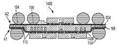
도 1 내지 도 19는 리세스된 영역(예를 들어, 영역(104) 내에 배치되는 반도체 기판(102)의 일부분, 이하에서는, 리세스된 영역(recessed region)(104)으로 지칭됨)이 구비된 반도체 기판(102)을 포함하는 다양한 예시적 패키지 조립체를 개략적으로 도시한다. 도 1은 다양한 실시예에 따른 패키지 조립체(100)의 구성을 도시한다. 패키지 조립체(100)는, 예를 들어 실리콘(Si)과 같은 반도체 물질을 상당량 포함하는 기판 또는 인터포저(interposer)인 반도체 기판(102)을 포함한다. 즉, 반도체 기판(102)의 대부분의 물질은 반도체 물질이다. 반도체 물질은 결정질 및/또는 비결정질 타입의 물질을 포함할 수 있다. 예를 들어, 실리콘의 경우에, 실리콘은 단결정 및/또는 폴리실리콘 타입을 포함할 수 있다. 다른 실시예에서, 반도체 기판(102)은, 본 명세서에서 설명되는 원리로부터 또한 혜택을 받을 수 있는, 예를 들어, 게르마늄, Ⅲ-Ⅴ족 물질, 또는 Ⅱ-Ⅵ족 물질과 같은, 다른 반도체 물질을 포함할 수 있다.1 through 19 illustrate a recessed region (e.g., a portion of a
반도체 기판(102)은 제 1 표면(A1)과, 그리고 제 1 표면(A1)의 반대편에 배치되는 제 2 표면(A2)을 포함한다. 제 1 표면(A1)과 제 2 표면(A2)은, 본 명세서에서 설명되는 다양한 구성에 대한 설명이 용이하도록 일반적으로 반도체 기판(102)의 양쪽 표면들을 의미한다.The
다양한 실시예에 따르면, 반도체 기판(102)의 리세스된 영역(104)이 형성되도록, 제 1 표면(A1)의 일부분은 제 1 표면(A1)의 다른 부분에 비해 리세스되어 있다. 리세스된 영역(104)은 일반적으로, 반도체 기판(102)을 뚫는 하나 이상의 비아들(108)의 형성이 용이하도록 반도체 기판(102)의 상대적으로 얇은 구역을 제공한다. 일부 실시예에서, 반도체 기판(102)은, 리세스된 영역(104)이 약 10 마이크로미터 내지 약 500 마이크로미터의 두께(T1)를 갖도록 리세스된다.According to various embodiments, a portion of the first surface A1 is recessed relative to another portion of the first surface A1 such that the
도 1의 반도체 기판(102)은 리세스된 영역(104) 외부의 두께가 더 두꺼운 반도체 기판(102)의 영역(106)을 포함하는바, 이 영역은 이하에서 두꺼운 영역(thicker region)(106)으로 지칭된다. 두꺼운 영역(106)에서의 반도체 기판(102)의 두께(T2)는 리세스된 영역(104)의 두께(T1)보다 크다.The
반도체 기판(102)은 다이 또는 칩 상에 집적 회로(IC) 구조물을 제조하기 위해 일반적으로 알려져 있는 기술과 유사한 기술을 이용하여 제조된다. 예를 들어, 다이 상에 IC 소자를 제조하기 위한 리소그래피/식각과 같은 잘 알려져 있는 패터닝 프로세스 및/또는 증착 프로세스가 반도체 기판(102)의 특징부를 형성하기 위해 사용될 수 있다. 반도체 제조 기술을 이용함으로써, 반도체 기판(102)은 적층체 (예를 들어, 유기질) 기판과 같은 다른 타입의 기판보다 더 작은 특징부를 포함할 수 있다. 반도체 기판(102)은 계속 크기가 축소되고 있는 현재의 다이에 대해 입력/출력(I/O) 및/또는 전력/접지 신호와 같은 전기적 신호들의 라우팅을 용이하게 한다. 예를 들어, 일부 실시예에서, 반도체 기판(102)은 정밀 피치 Si-Si 상호연결(fine pitch Si-to-Si interconnects)을 가능하게 하고, 반도체 기판(102)과 하나 이상의 다이들(112) 간의 최종 라인 라우팅(final line routing)을 가능하게 한다.The
다양한 실시예에 따르면, 반도체 기판(102)의 리세스된 영역(104)에 하나 이상의 비아들(108)이 형성된다. 하나 이상의 비아들(108)은 전기전도성 및/또는 열전도성 물질(예를 들어, 금속)로 충전된다. 하나 이상의 비아들의 금속과 반도체 기판의 반도체 물질 사이에 유전체 물질이 배치될 수 있다. 하나 이상의 비아들(108)은 일반적으로 반도체 기판(102)의 제 1 표면(A1)과 제 2 표면(A2) 간에 전기적 경로 또는 열적 경로를 제공한다. 반도체 기판(102)이 실리콘을 포함하는 실시예에서, 하나 이상의 비아들(108)은 하나 이상의 쓰루 실리콘 비아(Through-Silicon Via, TSV)들이다.According to various embodiments, one or
반도체 기판(102)에 결합된 하나 이상의 다이들(112)의 전기적 신호들을 라우팅시키기 위해, 반도체 기판(102)의 제 1 표면(A1) 및/또는 제 2 표면(A2) 상에는 하나 이상의 재분배층(redistribution layer)들(110)이 형성된다. 예를 들어, 하나 이상의 재분배층들(110)은 하나 이상의 다이들(112)과 하나 이상의 비아들(108) 간에 전기적 라우팅을 제공할 수 있음과 아울러 하나 이상의 비아들(108)과 하나 이상의 패키지 상호연결 구조물들(package interconnect structure)들(114) 간에 전기적 라우팅을 제공할 수 있다.One or more redistribution layers (not shown) may be formed on the first surface A1 and / or the second surface A2 of the
예를 들어, 하나 이상의 재분배층들(110)은, 예를 들어, 실리콘 다이옥사이드(SiO2), 실리콘 나이트라이드(SiN), 실리콘 옥시나이트라이드(SiOxNy), 또는 다른 적절한 유전체 물질을 포함하는 유전체 층을 반도체 기판(102)의 표면 상에 형성하고 이 유전체 층 상에 예를 들어, 금속(예컨대, 구리 혹은 알루미늄) 또는 도핑된 반도체 물질(예컨대, 도핑된 폴리실리콘)과 같은 전기전도성 물질을 증착 및/또는 패터닝함으로써 형성될 수 있다. 다른 실시예에서는, 하나 이상의 재분배층들(110)을 형성하기 위해 다른 적절한 전기전도성 물질이 이용될 수 있다.For example, one or more of the
하나 이상의 재분배층들(110)은 예를 들어, 패드(pad)들, 랜드(land)들, 또는 트레이스(trace)들과 같이, 전기적 신호들을 라우팅하기 위한 다양한 구조물을 포함할 수 있다. 도시되지는 않지만, 예를 들어 폴리이미드와 같은 전기절연성 물질을 포함하는 부동태화층(passivation layer)이, 하나 이상의 재분배층들(110) 상에 증착될 수 있고, 그리고 하나 이상의 다이들(112)과 하나 이상의 재분배층들(110)의 전기적 결합을 가능하게 하기 위해 부동태화층 내에 개구가 제공되도록 부동태화층이 패터닝될 수 있다.The one or
예를 들어, 도시된 바와 같은, 플립칩 구성을 포함하는 임의의 적절한 구성을 이용하여 하나 이상의 다이들(112)이 반도체 기판(102)에 결합된다. 다른 실시예에서는, 예를 들어, 와이어 본딩 구성(wire-bonding configuration)과 같은 다른 적절한 다이 부착 구성(die-attach configurations)이 사용될 수 있다. 도 1의 도시된 실시예에서, 하나 이상의 다이들(112)은 반도체 기판(102)의 리세스된 영역(104)의 제 1 표면(A1)에 결합된다.For example, one or
하나 이상의 다이들(112)은 일반적으로, 예를 들어 실리콘과 같은 반도체 물질을 포함한다. 일 실시예에서, 하나 이상의 다이들(112) 및 반도체 기판(102)은, 예를 들어 열팽창계수(Coefficients of Thermal Expansion, CTE)의 불일치와 같은, 물질의 가열/냉각 불일치 특성과 관련된 응력을 감소시키기 위해 동일한 반도체 물질을 이용하여 제조된다.The one or more dies 112 generally comprise a semiconductor material, such as, for example, silicon. In one embodiment, the one or more dies 112 and the
하나 이상의 다이들(112)은 일반적으로, 로직 및/또는 메모리를 위한 트랜지스터들과 같은 복수의 집적 회로(IC) 소자들(미도시)이 형성되는 표면을 포함하는 활성면(active side)과, 이러한 활성면의 반대편에 배치되는 비활성면(inactive side)을 갖는다. 하나 이상의 다이들(112)의 활성면은 하나 이상의 재분배층들(110)에 전기적으로 결합된다. 일부 실시예에서, 하나 이상의 다이들(112)의 활성면은, 도면에 도시된 바와 같이, 하나 이상의 범프들(bump)들(111)을 이용하여 하나 이상의 재분배층들(110)에 결합된다. 다른 실시예에서, 하나 이상의 다이들(112)의 활성면은 예를 들어, 하나 이상의 본딩 와이어(bonding wire)들과 같은 다른 구조물을 이용하여 하나 이상의 재분배층들(110)에 전기적으로 결합된다.The one or more dies 112 generally include an active side including a surface on which a plurality of integrated circuit (IC) elements (not shown), such as transistors and / or transistors for logic and / or memory, are formed, And has an inactive side disposed opposite the active surface. The active surface of one or more dies 112 is electrically coupled to one or more redistribution layers 110. In some embodiments, the active surface of one or more dies 112 is coupled to one or more redistribution layers 110 using one or
도 1의 도시된 실시예에서, 하나 이상의 범프들(111)은 하나 이상의 다이들(112) 상에 형성되어 하나 이상의 재분배층들(110)에 본딩된다. 하나 이상의 범프들(111)은 일반적으로 하나 이상의 다이들(112)의 전기적 신호들을 라우팅시키기 위해, 예를 들어, 땜납(solder) 또는 다른 금속과 같은 전기전도성 물질을 포함한다. 다양한 실시예에 따르면, 하나 이상의 범프들(111)은 납, 금, 주석, 구리, 또는 무연 물질, 또는 이들의 조합을 포함한다. 하나 이상의 범프들(111)은 구형, 원통형, 장방형, 또는 다른 형상을 포함하는 다양한 형태를 가질 수 있고, 예를 들어, 피제어 붕괴 칩 연결(Controlled Collapse Chip Connect, C4) 프로세스, 스터드 범핑(stud-bumping), 또는 다른 적절한 프로세스와 같은 범핑 프로세스(bumping process)를 이용하여 형성될 수 있다.In the depicted embodiment of FIG. 1, one or
하나 이상의 범프들(111)이 하나 이상의 다이들(112) 상에 형성될 수 있고, 이때, 하나 이상의 다이들(112)은 웨이퍼 형태 혹은 싱귤레이트(singulate)된 형태로 존재한다. 하나 이상의 다이들(112)이 반도체 기판(102)에 부착될 수 있고, 이때, 반도체 기판(102)은 웨이퍼 형태 또는 싱귤레이트된 형태로 존재한다.One or
도시되지는 않았지만, 하나 이상의 다른 능동 또는 수동 컴포넌트들이 반도체 기판(102) 상에 장착될 수 있다. 컴포넌트들은 전자 화합물(Electronic Compound)들 및 집적 회로(IC)들을 포함할 수 있다. 컴포넌트는, 예를 들어, 필터 컴포넌트, 저항, 인덕터, 전력 증폭기, 커패시터, 또는 패키징된 IC를 포함할 수 있다. 다른 실시예에서는 다른 능동 또는 수동 컴포넌트들이 반도체 기판(102)에 결합될 수 있다.Although not shown, one or more other active or passive components may be mounted on the
예를 들어, 하나 이상의 땜납 볼(solder ball)들, 금속 기둥(metal post)들, 또는 범프들과 같은 하나 이상의 패키지 상호연결 구조물들(114)이, 하나 이상의 다이들(112)의 전기적 신호들을 추가적으로 라우팅시키기 위해, 하나 이상의 재분배층들(110) 상에 형성될 수 있다. 도 1의 도시된 실시예에서, 하나 이상의 패키지 상호연결 구조물들(114)은 반도체 기판(102)의 제 2 표면(A2) 상에 형성되는 하나 이상의 재분배층들(110)에 결합된다. 하나 이상의 패키지 상호연결 구조물들(114)은 일반적으로 전기전도성 물질을 포함한다. 하나 이상의 패키지 상호연결 구조물들(114)은 구형, 평면형, 또는 다각형 형상을 포함하는 다양한 형태로 형성될 수 있고, 다양한 위치에, 예를 들어, 일 열로 또는 복수의 열로 구성된 배열로 배치될 수 있다. 하나 이상의 패키지 상호연결 구조물들(114)이 반도체 기판(102)의 주변부 상에 도시되어 있지만, 다른 실시예에서는 반도체 기판(102)의 중앙에 또는 중앙 근처에 하나 이상의 패키지 상호연결 구조물들(114)이 배치될 수 있다.For example, one or more
도 2는 다양한 실시예에 따른, 또 다른 구성의 패키지 조립체(200)를 도시한다. 패키지 조립체(200)는 반도체 기판(102)의 양쪽 표면들에 결합된 하나 이상의 다이들을 갖는다. 하나 이상의 다이들(112)은 반도체 기판(102)의 제 1 표면(A1)과 반도체 기판의 제 2 표면(A2) 상의 하나 이상의 재분배층들(110)에 결합된다. 패키지 조립체(200)에서 반도체 기판(102)의 양면에는 하나 이상의 다이들(112)이 결합될 수 있다. 도 2의 도시된 실시예에서, 제 1 표면(A1) 상의 하나 이상의 다이들(112)은 반도체 기판(102)의 동일한 리세스된 영역(104)에 결합된다.Figure 2 illustrates a further
패키지 조립체(200)는, 하나 이상의 반도체 다이들(112)의 전기적 신호들을 다른 전자 소자(250)로 추가적으로 라우팅시키기 위해, 반도체 기판(102)의 제 2 표면(A2) 상에 배치되는 하나 이상의 패키지 상호연결 구조물들(114)을 이용하여 인쇄 회로 보드(PCB)(예를 들어, 마더보드), 모듈, 또는 다른 패키지 조립체와 같은 다른 전자 소자(250)에 전기적으로 결합될 수 있다.The
도 3은 다양한 실시예에 따른, 또 다른 구성의 패키지 조립체(300)를 도시한다. 패키지 조립체(300)는, 반도체 기판(102)을 또 다른 전자 소자(250)에 전기적으로 결합시키기 위해, 반도체 기판(102)의 제 1 표면(A1) 상에 형성되는 하나 이상의 패키지 상호연결 구조물들(114)을 갖는다. 즉, 하나 이상의 패키지 상호연결 구조물들(114)은, 리세스된 영역(104)이 형성되도록 리세스된 표면과 동일한 표면(예를 들어, 도 3의 제 1 표면(A1))에 결합될 수 있다.FIG. 3 illustrates a
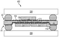
도 4는 다양한 실시예에 따른, 또 다른 구성의 패키지 조립체(400)를 도시한다. 패키지 조립체(400)는 반도체 기판(102)의 제 1 표면(A1)과 제 2 표면(A2) 상에 배치되는 하나 이상의 패키지 상호연결 구조물들(114)을 갖는다. 패키지 조립체(400)에서, 제 1 표면(A1) 상에 배치되는 하나 이상의 패키지 상호연결 구조물들(114)을 이용하여 또 다른 전자 소자(250)가 제 1 표면(A1)에 결합될 수 있고, 제 2 표면(A2) 상에 배치되는 하나 이상의 패키지 상호연결 구조물들(114)을 이용하여 또 다른 전자 소자(250)가 제 2 표면(A2)에 결합될 수 있다. 예를 들어, 일 실시예에서, 제 1 표면(A1)에 결합된 또 다른 전자 소자(250)는 인쇄 회로 보드이고, 표면 (A2)에 결합된 또 다른 전자 소자(250)는 또 다른 패키지 조립체이다. 패키지 조립체(400)는 다양한 다층 패키지-온-패키지(Package-On-Package, POP) 혹은 또 다른 3차원(3D) 패키징 구성으로 구성될 수 있다.FIG. 4 illustrates a
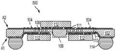
도 5는 다양한 실시예에 따른, 또 다른 구성의 패키지 조립체(500)를 도시한다. 패키지 조립체(500)는, 반도체 기판(102)의 제 1 표면(A1)에 형성되는, 제 1 리세스된 영역인 리세스된 영역(104)과, 제 2 리세스된 영역인 적어도 하나의 또 다른 리세스된 영역(504)을 갖는다. 리세스된 영역(104)은 제 1 표면(A1)의 제 1 부분을 리세스시킴으로써 형성될 수 있고, 다른 리세스된 영역(504)은 제 1 표면(A1)의 제 2 부분을 리세스시킴으로써 형성될 수 있다. 리세스된 영역(104) 및 다른 리세스된 영역(504)은 반도체 기판(102)의 두꺼운 영역(106)에 의해 분리된다. 두꺼운 영역(106)은 제조, 패키징, 및/또는 조립체 동작 동안, 패키지 조립체(500)에 대해 상대적으로 강한 기계적 지지를 제공한다.Figure 5 illustrates a further
도시된 실시예에서, 리세스된 영역(104)과 다른 리세스된 영역(504)에 하나 이상의 비아들(108)이 형성되고, 그리고 리세스된 영역(104)과 다른 리세스된 영역(504) 각각에 하나 이상의 다이들(112) 중 적어도 하나의 다이가 배치된다. 다른 실시예에서는 추가적인 리세스된 영역들이 사용될 수 있다.In the illustrated embodiment, one or
도 6은 다양한 실시예에 따른, 또 다른 구성의 패키지 조립체(600)를 도시한다. 패키지 조립체(600)의 반도체 기판(102)은 리세스된 영역(104)이 형성되도록 리세스된 제 1 표면(A1)을 갖는다. 하나 이상의 다이들(112)이 반도체 기판(102)의 제 2 표면(A2) 상에 배치된다. 도시된 실시예에서, 하나 이상의 다이들(112)은, 제 1 표면(A1)에 대해 실질적으로 평탄한, 반도체 기판(102)의 리세스된 영역(104)의 제 2 표면(A2)에 결합된다. 하나 이상의 패키지 상호연결 구조물들(114)이, 볼 그리드 어레이(Ball-Grid Array, BGA) 구성을 포함하는 다양한 구성으로 배열될 수 있다.Figure 6 illustrates a further
도 7은 다양한 실시예에 따른, 또 다른 구성의 패키지 조립체(700)를 도시한다. 패키지 조립체(700)는, 반도체 기판(102)의 제 1 표면(A1)에 형성되는, 제 1 리세스된 영역인 리세스된 영역(104)과, 제 2 리세스된 영역인 적어도 하나의 또 다른 리세스된 영역(504)을 갖는다. 리세스된 영역(104) 및 다른 리세스된 영역(504)은 반도체 기판(102)의 두꺼운 영역(106)에 의해 분리된다.Figure 7 illustrates a further
하나 이상의 다이들(112)이, 리세스된 영역(104)의 제 1 표면(A1)에 결합되고, 그리고 하나 이상의 패키지 상호연결 구조물들(114)이 다른 리세스된 영역(504)의 제 1 표면(A1)에 결합된다. 다른 리세스된 영역(504)에 결합되는 하나 이상의 패키지 상호연결 구조물들(114)을 갖는 패키지 조립체(700)는, 도시된 바와 같이, 두꺼운 영역(예를 들어, 두꺼운 영역(106))에 결합되는 하나 이상의 패키지 상호연결 구조물들을 갖는 패키지 조립체보다 더 얇은 패키지 조립체(700)를 제공한다. 도시된 실시예에서, 하나 이상의 패키지 상호연결 구조물들(114)은 반도체 기판(102)의 제 1 표면(A1) 상에 형성되는 하나 이상의 재분배층들(110)을 이용하여 하나 이상의 다이들(112)에 전기적으로 결합된다.One or more dies 112 are coupled to the first surface A1 of the recessed
도 8은 다양한 실시예에 따른, 또 다른 구성의 패키지 조립체(800)를 도시한다. 패키지 조립체(800)는 도 7의 패키지 조립체(700)와 유사하게, 리세스된 영역(104), 또 다른 리세스된 영역(504), 및 두꺼운 영역(106)을 포함한다. 패키지 조립체(800)는 또한, 하나 이상의 패키지 상호연결 구조물들(114)을 하나 이상의 다이들(112)에 전기적으로 결합시키기 위해 다른 리세스된 영역(504)에 형성되는 하나 이상의 비아들(108)을 포함한다. 다른 리세스된 영역(504)에 배치되는 하나 이상의 비아들(108)은, 도시된 바와 같이, 리세스된 영역(104)에 배치되는 하나 이상의 비아들(108)과 그리고 제 2 표면(A2) 상에 형성되는 적어도 하나 이상의 재분배층들(110)을 통해 하나 이상의 다이들(112)에 전기적으로 결합된다.Figure 8 illustrates a further
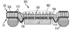
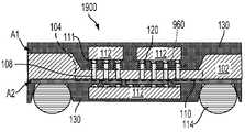
도 9는 다양한 실시예에 따른, 또 다른 구성의 패키지 조립체(900)를 도시한다. 패키지 조립체(900)는 도 7 및 도 8과 관련하여 설명된 바와 유사하게, 리세스된 영역(104), 또 다른 리세스된 영역(504), 및 두꺼운 영역(106)을 포함한다. 도 9에서, 반도체 기판(102)의 제 2 표면(A2)의 적어도 일부분은 리세스되어, 리세스된 영역(104)에 배치되는 하나 이상의 비아들(108)이 노출되고, 이에 따라, 하나 이상의 비아들(108)이 제 2 표면(A2)의 리세스된 부분 너머로 연장되어, 하나 이상의 비아들(108)의 연장된 부분(extended portion)(960)을 정의한다. 하나 이상의 비아들(108)의 연장된 부분(960)은, 하나 이상의 다이들(112)로부터의 열 제거를 용이하게 하기 위한 방열체(heat sink)의 하나 이상의 핀(fin)들로서의 기능을 할 수 있다.FIG. 9 illustrates a
도 10은 다양한 실시예에 따른, 또 다른 구성의 패키지 조립체(1000)를 도시한다. 패키지 조립체(1000)는, 반도체 기판(102)의 제 2 표면(A2)의 적어도 일부분을 리세스시킴으로써 형성되는, 하나 이상의 비아들(108)의 연장된 부분(960)을 포함한다. 예를 들어, 옥사이드를 포함하는 유전체 라이너(dielectric liner)(120) 또는 유전체 막이 하나 이상의 비아들(108)의 전기전도성 및/또는 열전도성 물질 상에 배치된다. 유전체 라이너(120)는 예를 들어, 하나 이상의 비아들(108)을 노출시키기 위해 반도체 기판의 제 2 표면(A2)을 리세스시키는 프로세스(예를 들어, 식각)로부터 하나 이상의 비아들(108)의 전기전도성 및/또는 열전도성 물질을 보호하기 위한 보호층으로서의 역할을 할 수 있다. 하나 이상의 다이들(112)이, 도시된 바와 같이, 하나 이상의 범프들(111)을 이용하여 하나 이상의 비아들(108)의 연장된 부분(960)에 전기적으로 결합될 수 있다.FIG. 10 illustrates a
도 11은 다양한 실시예에 따른, 또 다른 구성의 패키지 조립체(1100)를 도시한다. 패키지 조립체(1100)는, 도시된 바와 같이, 리세스된 영역(104) 및 두꺼운 영역(106)을 포함한다. 하나 이상의 선택적으로 리세스된 구역들(113)(예를 들어, 홀(hole)들 또는 채널(channel)들)이 두꺼운 영역(106)의 표면 상에 형성되어, 반도체 기판의 표면적을 증가시키고, 이에 따라, 패키지 조립체(1100)의 열원(heat source)들로부터의 방열(heat dissipation)을 용이하게 한다.Figure 11 illustrates a further
도 12는 다양한 실시예에 따른, 또 다른 구성의 패키지 조립체(1200)를 도시한다. 패키지 조립체(1200)는, 도시된 바와 같이, 리세스된 영역(104), 또 다른 리세스된 영역(504), 그리고 리세스된 영역(104)과 또 다른 리세스된 영역(504) 사이에 배치되는 두꺼운 영역(106)을 포함한다. 리세스된 영역(104) 및 다른 리세스된 영역(504)에 하나 이상의 비아들(108)이 형성된다. 리세스된 영역(104) 및 다른 리세스된 영역(504)의 제 1 표면(A1) 상에 하나 이상의 패키지 상호연결 구조물들(114) 중 적어도 하나의 패키지 상호연결 구조물이 배치된다. 이러한 구성은 패키지 조립체(1200)의 총 높이 또는 두께를 감소시킬 수 있다. 도시된 바와 같이, 하나 이상의 다이들(112)이 제 1 표면(A1) 및/또는 두꺼운 영역(106)의 제 2 표면(A2)에 결합된다.Figure 12 illustrates a further
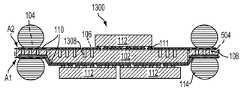
도 13은 다양한 실시예에 따른, 또 다른 구성의 패키지 조립체(1300)를 도시한다. 패키지 조립체(1300)는 반도체 기판(102)을 완전히 뚫는 하나 이상의 비아들(108)을 포함한다. 즉, 반도체 기판(102)의 제 1 표면(A1)과 제 2 표면(A2) 간의 연속적인 전기적 혹은 열적 연결부를 형성하기 위해, 하나 이상의 비아들(108)이, 리세스된 영역(104) 및 다른 리세스된 영역(504)에 형성된다. 하나 이상의 추가적인 비아들(1308)이 반도체 기판(102)의 두꺼운 영역(106)의 제 2 표면(A2)에 형성된다. 하나 이상의 추가적인 비아들(1308)은 반도체 기판(102)을 완전히 뚫지 않는다. 즉, 도시된 실시예에서, 하나 이상의 추가적인 비아들(1308)은 반도체 기판(102)의 제 2 표면(A2) 상에만 배치되고, 제 1 표면(A1)에는 도달하지 않는다. 하나 이상의 추가적인 비아들(1308)은 패키지 조립체(1300)에서 열에 대한 열적 경로를 제공함으로써 열 제거를 용이하게 하는 핑거 구조물(finger structure)들을 제공한다.Figure 13 shows a further
도 14는 다양한 실시예에 따른, 또 다른 구성의 패키지 조립체(1400)를 도시한다. 패키지 조립체(1400)는 반도체 기판(102)의 두꺼운 영역(106)의 제 1 표면(A1)에 형성되는 하나 이상의 추가적인 비아들(1308)을 포함한다. 하나 이상의 추가적인 비아들(1308)은 반도체 기판(102)을 완전히 뚫지 않는다. 즉, 도시된 실시예에서, 하나 이상의 추가적인 비아들(1308)은 반도체 기판(102)의 제 1 표면(A1) 상에만 배치되고 제 2 표면(A2)에는 도달하지 않는다. 하나 이상의 추가적인 비아들(1308)은 패키지 조립체(1400)에서 열에 대한 열적 경로를 제공함으로써 열 제거를 용이하게 하는 핑거 구조물들을 제공한다.FIG. 14 illustrates a
도 15는 다양한 실시예에 따른, 또 다른 구성의 패키지 조립체(1500)를 도시한다. 패키지 조립체(1500)는, 도시된 바와 같이, 반도체 기판(102)의 제 2 표면(A2)에 형성되는 리세스된 영역(104) 및 또 다른 리세스된 영역(504)을 포함한다. 도시된 바와 같이, 반도체 기판(102)의 제 1 표면(A1)의 적어도 일부분을 리세스시킴으로써 추가적인 리세스된 영역(1504)이 형성된다. 도시된 바와 같이, 리세스된 영역(104), 다른 리세스된 영역(504), 및 추가적인 리세스된 영역(1504)에 하나 이상의 비아들(108)이 배치된다. 리세스된 영역(104) 및 다른 리세스된 영역(504)의 제 2 표면(A2) 상에 하나 이상의 패키지 상호연결 구조물들(114)이 배치된다. 추가적인 리세스된 영역(1504)의 제 1 표면(A1) 상에 하나 이상의 다이들(112)이 배치된다. 이러한 구성은 높이 또는 두께가 감소된 패키지 조립체(1500)를 제공한다.FIG. 15 illustrates a
도 16은 다양한 실시예에 따른, 또 다른 구성의 패키지 조립체(1600)를 도시한다. 패키지 조립체(1600)는 도 15의 패키지 조립체(1500)의 반도체 기판(102)과 유사한 방식으로 구성된 반도체 기판(102)을 포함한다. 패키지 조립체(1600)는, 도시된 바와 같이, 반도체 기판(102) 상에 적층되는 또 다른 반도체 기판(1602)을 더 포함한다. 다른 반도체 기판(1602)은, 도시된 바와 같이, 다른 반도체 기판(1602)의 제 2 표면(A2)에 형성되는 리세스된 영역(104) 및 또 다른 리세스된 영역(504)을 포함한다. 도시된 바와 같이, 다른 반도체 기판(1602)의 제 1 표면(A1)에 추가적인 리세스된 영역(1504)이 형성된다. 추가적인 리세스된 영역(1504)에 하나 이상의 비아들(108)이 형성되고, 그리고 하나 이상의 반도체 다이들(112)이 추가적인 리세스된 영역(1504)에 배치되는 하나 이상의 비아들(108)에 전기적으로 결합된다.Figure 16 illustrates another
다양한 실시예에 따르면, 반도체 기판(102)의 제 2 표면(A2)은 다른 반도체 기판(1602)의 제 2 표면(A2)에 결합된다. 반도체 기판(102) 및 다른 반도체 기판(1602)은, 도시된 바와 같이, 예를 들어 하나 이상의 패키지 상호연결 구조물들(114)을 이용하여 결합될 수 있다. 다른 실시예에서는 반도체 기판(102)과 다른 반도체 기판(1602) 사이에 다른 타입의 전기적 또는 구조적 연결들이 있을 수 있다.According to various embodiments, the second surface A2 of the
도 17은 다양한 실시예에 따른, 또 다른 구성의 패키지 조립체(1700)를 도시한다. 패키지 조립체(1700)는 도 4의 패키지 조립체(400)의 반도체 기판(102)과 유사한 방식으로 구성된 반도체 기판(102)을 포함한다. 패키지 조립체(1700)는 반도체 기판(102)의 제 1 표면(A1) 및/또는 제 2 표면(A2) 상에 배치되는 몰딩 화합물(130)을 더 포함한다. 일부 실시예에서, 몰딩 화합물(130)은 하나 이상의 반도체 다이들(112)을 실질적으로 밀봉하도록 배치된다. 몰딩 화합물(130)은 일반적으로, 습기, 산화, 또는 처리와 관련된 칩핑(chipping)으로부터 하나 이상의 반도체 다이들(112)을 보호한다.Figure 17 shows a further
몰딩 화합물(130)은, 일부 실시예에서, 언더필 물질(underfill material)(미도시)과 함께 사용될 수 있다. 예를 들어, 언더필 물질은 하나 이상의 범프들(111)을 밀봉하기 위해 하나 이상의 다이들(112)과 반도체 기판(102) 사이에 배치될 수 있고, 그리고 몰딩 화합물(130)은 하나 이상의 다이들(112)을 밀봉하도록 배치될 수 있다. 일부 실시예에서, 몰딩 화합물(130)은 하나 이상의 다이들(112)로부터 방열을 용이하게 하기 위해 하나 이상의 다이들(112)의 표면이 노출되도록 형성될 수 있다. 몰딩 화합물(130)은 반도체 기판(102) 및/또는 하나 이상의 다이들(112)의 열팽창계수와 실질적으로 동일하거나 유사한 열팽창계수를 갖도록 선택될 수 있다.The
도 18은 다양한 실시예에 따른, 또 다른 구성의 패키지 조립체(1800)를 도시한다. 패키지 조립체(1800)는 반도체 기판(102)에 결합되는 하나 이상의 다이들(112)을 포함한다. 하나 이상의 다이들(112) 중 하나의 다이는, 도시된 바와 같이, 다이의 비활성 표면을 반도체 기판의 제 2 표면(A2)에 부착시키기 위해 접착제(142)를 이용하여 반도체 기판에 결합된다. 하나 이상의 본딩 와이어들(140)이, 도시된 바와 같이, 다이의 활성 표면을 하나 이상의 재분배층들(110)에 전기적으로 결합시킨다.18 illustrates a
몰딩 화합물(130)은, 도시된 바와 같이, 하나 이상의 다이들(112) 및 하나 이상의 본딩 와이어들(140)을 실질적으로 밀봉하도록 배치된다. 다양한 실시예에서는, 플립칩 구성과 와이어 본딩 구성의 다른 조합이 사용될 수 있거나 단지 와이어 본딩 구성만이 사용될 수 있다.The
도 19는 다양한 실시예에 따른, 또 다른 구성의 패키지 조립체(1900)를 도시한다. 반도체 기판(102)은 제 1 표면(A1)에 형성되는 리세스된 영역(104)과, 그리고 리세스된 영역(104)에 형성되는 하나 이상의 비아들(108)을 포함한다. 제 1 표면(A1)은 하나 이상의 비아들(108)의 연장된 부분(960)이 노출되도록 리세스된다. 유전체 라이너(120)가, 도시된 바와 같이, 하나 이상의 비아들(108)의 전기전도성 및/또는 열전도성 물질 상에 배치된다. 하나 이상의 다이들(112)이, 도시된 바와 같이, 하나 이상의 비아들(108)의 연장된 부분(960)에 결합된다. 몰딩 화합물(130)이, 도시된 바와 같이, 하나 이상의 다이들(112)을 실질적으로 밀봉함과 아울러 하나 이상의 반도체 다이들과 반도체 기판(102) 사이의 영역을 충전하도록 배치된다.19 illustrates a
본 명세서에서 설명되는 바와 같이 반도체 기판을 이용하는 패키지 조립체에 대한 구성은 여러 이점들, 즉 반도체 기판에 하나 이상의 비아들을 제조하는 것과 관련된 프로세스 복잡도 및/또는 비용을 감소시킬 수 있다는 이점, 반도체 기판의 양면 활용이 가능하다는 이점, 다층 패키지 구성이 용이하다는 이점, 패키지 조립체의 크기를 감소시킬 수 있다는 이점, 그리고/또는 방열 능력을 증가시킬 수 있다는 이점을 제공할 수 있다. 본 개시내용의 범위는 도 1 내지 도 19와 연계하여 설명된 실시예들의 임의의 적절한 조합을 포함한다.The configuration for a package assembly using a semiconductor substrate as described herein can be advantageous in that it can reduce the process complexity and / or costs associated with manufacturing one or more vias in a semiconductor substrate, The advantage of being able to be utilized, the advantage of being easy to construct a multi-layer package, the advantage of being able to reduce the size of the package assembly, and / or the ability to increase heat dissipation capability. The scope of this disclosure includes any suitable combination of embodiments described in connection with Figs. 1-19.
도 20은 리세스된 영역(예를 들어, 도 1의 리세스된 영역(104))이 구비된 반도체 기판(예를 들어, 도 1의 반도체 기판(102))을 포함하는 패키지 조립체(예를 들어, 도 1의 패키지 조립체(100))를 제조하기 위한 방법(2000)의 프로세스 순서도다. 단계(2002)에서, 방법(2000)은 반도체 기판을 제공하는 단계를 포함한다. 반도체 기판은 제 1 표면(예를 들어, 도 1의 제 1 표면(A1))과, 제 1 표면의 반대편에 배치되는 제 2 표면(예를 들어, 도 1의 제 2 표면(A2))을 갖는다. 반도체 기판은 예를 들어, 실리콘과 같은 반도체 물질을 포함한다. 반도체 기판은 예를 들어, 단결정 또는 다결정 반도체 물질의 잉곳(ingot)으로부터 절개될 수 있다. 방법(2000)과 관련하여 설명되는 프로세스 동안, 반도체 기판은 싱귤레이트된 형태나 웨이퍼 형태로 존재할 수 있다.Figure 20 illustrates a package assembly (e.g., a semiconductor package) including a semiconductor substrate (e.g.,
단계(2004)에서, 방법(2000)은 하나 이상의 리세스된 영역(예를 들어, 도 1의 리세스된 영역(104))이 형성되도록 반도체 기판을 리세스시키는 단계를 더 포함한다. 반도체 기판으로부터 반도체 물질을 제거하여 두께가 얇은 리세스된 영역이 제공되도록 반도체 기판의 표면의 적어도 일부분이 리세스되는바, 리세스된 영역의 두께가 얇기 때문에 리세스된 영역을 뚫는 하나 이상의 비아들의 형성이 용이하다. 반도체 기판의 표면은, 예를 들어, 실리콘 습식 식각 프로세스와 같은 잘 알려진 식각 프로세스를 포함하는 임의의 적절한 프로세스를 이용하여 리세스될 수 있다.In
일부 실시예에서는, 제 1 표면의 단지 일부분만이 리세스된다. 다른 실시예에서는, 본 명세서에서 설명되는 바와 같이, 복수의 리세스된 영역들을 갖는 패키지 조립체 구성을 제공하기 위해, 제 1 표면의 일부분 및/또는 제 2 표면의 일부분이 리세스된다. 다양한 실시예에 따르면, 리세스된 영역(들)의 두께는 리세스된 영역(들)의 외부에 위치한 반도체 기판의 영역(예를 들어, 도 1의 두꺼운 영역(106))의 두께보다 더 작다.In some embodiments, only a portion of the first surface is recessed. In another embodiment, a portion of the first surface and / or a portion of the second surface is recessed to provide a package assembly configuration having a plurality of recessed regions, as described herein. According to various embodiments, the thickness of the recessed region (s) is less than the thickness of the region of the semiconductor substrate located outside of the recessed region (s) (e.
단계(2006)에서, 방법(2000)은 반도체 기판에 하나 이상의 비아들(예를 들어, 도 1의 하나 이상의 비아들(108))을 형성하는 단계를 더 포함한다. 반도체 기판의 제 1 표면과 제 2 표면 간에 전기적 경로 및/또는 열적 경로를 제공하기 위해, 일반적으로 하나 이상의 비아들이, 리세스된 영역(들)에 형성된다. 다양한 실시예에 따르면, 하나 이상의 비아들은 쓰루 실리콘 비아(TSV)들을 포함한다.At
하나 이상의 비아들은 일반적으로, 반도체 기판을 뚫는 하나 이상의 채널들이 형성되도록, 리세스된 영역으로부터 반도체 물질을 제거함으로써 형성된다. 리세스된 영역으로부터 반도체 물질을 제거하는 레이저 드릴링 및/또는 식각 프로세스를 포함하는 여러 가지 적절한 프로세스들이 하나 이상의 채널들을 형성하는데 사용될 수 있다. 리세스된 영역은, 반도체 기판을 완전히 뚫는 하나 이상의 비아들의 드릴링 또는 식각이 가능한 반도체 물질의 두께를 제공함으로써, 하나 이상의 비아들의 형성을 용이하게 할 수 있다. 비아가 반도체 기판의 제 1 면이나 제 2 면으로부터 물질을 제거함으로써 형성될 수 있지만, 더 평면적인 표면 즉, 평탄한 표면(예를 들어, 도 1의 제 2 표면(A2))으로부터 물질을 제거함으로써 비아 형성 프로세스가 용이하게 수행될 수 있다.The one or more vias are typically formed by removing semiconductor material from the recessed regions such that one or more channels are formed through the semiconductor substrate. Various suitable processes may be used to form one or more channels, including laser drilling and / or etching processes to remove semiconductor material from the recessed regions. The recessed region can facilitate the formation of one or more vias by providing a thickness of a drillable or etchable semiconductor material of one or more vias that completely punch the semiconductor substrate. Although vias can be formed by removing material from the first or second side of the semiconductor substrate, by removing material from a more planar surface, i.e., a planar surface (e.g., second surface A2 in FIG. 1) The via formation process can be easily performed.
하나 이상의 채널들이 형성된 이후, 유전체 막이 하나 이상의 채널들의 표면 상에 형성될 수 있다. 유전체 막은, 예를 들어, 실리콘 다이옥사이드(SiO2), 실리콘 나이트라이드(SiN), 또는 실리콘 옥시나이트라이드(SiOxNy)(여기서 x와 y는 적절한 화학양론적 값을 나타냄)와 같은 유전체 물질이 증착되도록, 물리적 기상 증착(Physical Vapor Deposition, PVD), 화학적 기상 증착(Chemical Vapor Deposition, CVD), 및/또는 원자층 증착(Atomic Layer Deposition, ALD)과 같은 증착 기술을 이용함으로써 형성될 수 있다. 다른 실시예에서는 다른 적절한 증착 기술 및/또는 유전체 물질이 사용될 수 있다. 유전체 막은 일반적으로, 하나 이상의 비아들에 배치되는 전기전도성 물질을 전기적으로 격리시켜, 반도체 기판의 반도체 물질(예를 들어, 실리콘)과 전기전도성 물질 간의 전류 누설을 방지한다.After one or more channels are formed, a dielectric film may be formed on the surface of one or more channels. Dielectric materials such as dielectric film, for example, silicon dioxide (SiO2), (where x and y represent the appropriate stoichiometric value), silicon nitride (SiN), or silicon oxynitride (SiOx Ny) May be formed by using deposition techniques such as physical vapor deposition (PVD), chemical vapor deposition (CVD), and / or atomic layer deposition (ALD) . Other suitable deposition techniques and / or dielectric materials may be used in other embodiments. The dielectric film generally electrically isolates the electrically conductive material disposed in the one or more vias to prevent current leakage between the semiconductor material (e.g., silicon) and the electrically conductive material of the semiconductor substrate.
예를 들어, 구리 혹은 또 다른 금속과 같은 전기전도성 및/또는 열전도성 물질이 하나 이상의 채널들에 증착된다. 일 실시예에서, 전기전도성 및/또는 열전도성 물질은 하나 이상의 채널들을 실질적으로 충전하도록 증착된다. 또 다른 실시예에서, 전기전도성 및/또는 열전도성 물질은, 하나 이상의 채널들의 표면 상의 유전체 막을 코팅하기 위해 증착되며, 그리고 예를 들어, 에폭시, 수지, 또는 옥사이드와 같은 전기절연성 물질이, 하나 이상의 채널들의 나머지 부분을 충전하기 위해 증착된다.For example, electrically conductive and / or thermally conductive materials such as copper or another metal are deposited on one or more channels. In one embodiment, the electrically conductive and / or thermally conductive material is deposited to substantially fill one or more channels. In yet another embodiment, the electrically conductive and / or thermally conductive material is deposited to coat a dielectric film on the surface of one or more channels and an electrically insulating material, such as, for example, epoxy, resin, or oxide, To deposit the remaining portions of the channels.
하나 이상의 비아들은, 반도체 기판에 결합되는 하나 이상의 다이들의 전기적 신호들을 라우팅시키기 위해 사용될 수 있다. 일부 실시예에서, 방열의 용이하도록, 하나 이상의 비아들(예를 들어, 도 13의 하나 이상의 추가적인 비아들(1308))이 반도체 기판의 두꺼운 영역(예를 들어, 도 13의 두꺼운 영역(106))에 형성된다. 이러한 비아는 일반적으로, 반도체 기판의 제 1 표면과 제 2 표면 중 단지 하나의 표면 상에만 배치된다. 즉, 두꺼운 영역에 형성되는 하나 이상의 비아들은 반도체 기판을 완전히 뚫지 않는다.The one or more vias may be used to route electrical signals of one or more dies coupled to a semiconductor substrate. In some embodiments, one or more vias (e.g., one or more
일부 실시예에서, 반도체 기판의 표면은 하나 이상의 비아들의 형성 이후 리세스되는바, 이에 따라 반도체 기판의 리세스된 표면 너머로 연장되는 하나 이상의 비아들의 연장된 부분(예를 들어, 도 9의 연장된 부분(960))이 제공되게 된다. 하나 이상의 비아들의 하나 이상의 채널들의 표면 상에 배치되는 유전체 막(예를 들어, 도 10의 유전체 라이너(120))은, 연장된 부분을 노출시키는데 사용되는 식각 프로세스로부터 하나 이상의 비아들의 전기전도성 및/또는 열전도성 물질을 보호할 수 있다. 하나 이상의 비아들의 전기전도성 및/또는 열전도성 물질과 하나 이상의 다이들의 결합이 용이하도록 유전체 막의 일부분을 제거하기 위해, 스페이서 식각 프로세스(spacer etch process)와 같은 또 다른 식각 프로세스가 이용될 수 있다.In some embodiments, the surface of the semiconductor substrate is recessed after formation of one or more vias, thereby forming an extended portion of one or more vias extending beyond the recessed surface of the semiconductor substrate (e.g., Portion 960). A dielectric film (e.g.,
단계(2008)에서, 방법(2000)은 반도체 기판 상에 재분배층(예를 들어, 도 1의 하나 이상의 재분배층들(110))을 형성하는 단계를 더 포함한다. 재분배층은 일반적으로, 반도체 기판의 표면 상에 유전체 막을 증착하고 유전체 막 상에 전기전도성 물질을 증착함으로써 형성된다. 일부 실시예에서, 유전체 막은 하나 이상의 비아들을 형성하기 위한 유전체 막의 증착과 동시에 증착된다. 증착된 전기전도성 물질은, 하나 이상의 다이들의 전기적 신호들을 라우팅시키는 재분배층의 라우팅 구조를 제공하도록 패터닝 및/또는 식각될 수 있다. 전기적 신호들의 원하는 라우팅을 제공하기 위해, 복수의 재분배층들이 반도체 기판의 제 1 표면 및/또는 제 2 표면 상에 적층될 수 있다.In
단계(2010)에서, 방법(2000)은 반도체 기판에 하나 이상의 다이들을 결합시키는 단계를 더 포함한다. 하나 이상의 다이들은 예를 들어, 플립칩 구성 또는 와이어본딩 구성 또는 이들의 조합을 포함하는 다양한 구성으로 반도체 기판에 결합될 수 있다. 플립칩 구성에서, 다이의 활성 표면은 하나 이상의 범프들(예를 들어, 도 1의 하나 이상의 범프들(111))을 이용하여 재분배층에 결합된다. 와이어본딩 구성에서, 다이의 비활성 표면은 접착제(예를 들어, 도 18의 접착제(142))를 이용하여 반도체 기판에 결합되고, 다이의 활성 표면은 하나 이상의 본딩 와이어들(140)을 이용하여 재분배층에 결합된다. 하나 이상의 다이들은 반도체 기판의 리세스된 영역(들)에 형성된 하나 이상의 비아들에 전기적으로 결합된다.In
하나 이상의 다이들은 반도체 기판의 제 1 표면 및/또는 제 2 표면에 결합될 수 있다. 더욱이, 하나 이상의 다이들은 다양한 실시예에 따라, 반도체 기판의 리세스된 영역(들) 또는 두꺼운 영역(들)에 결합될 수 있다.One or more dies may be coupled to the first surface and / or the second surface of the semiconductor substrate. Moreover, the one or more dies may be coupled to the recessed region (s) or the thicker region (s) of the semiconductor substrate, according to various embodiments.
단계(2012)에서, 방법(2000)은 반도체 기판에 하나 이상의 패키지 상호연결 구조물들(예를 들어, 도 1의 하나 이상의 패키지 상호연결 구조물들(114))을 결합시키는 단계를 더 포함한다. 하나 이상의 패키지 상호연결 구조물들은 예를 들어, 스크린 인쇄(screen printing), 전기도금(electrical plating), 배선(placement), 또는, 다른 잘 알려진 방법들을 포함하는 여러 가지 적절한 프로세스들에 의해 형성될 수 있다. 하나 이상의 패키지 상호연결 구조물들이 반도체 기판의 제 1 표면과 제 2 표면 중 한 표면 혹은 양쪽 표면들 상의 재분배층(들)에 전기적으로 결합되어, 하나 이상의 다이들의 전기적 신호들이 패키지 조립체로 라우팅되거나 혹은 패키지 조립체로부터 또 다른 전자 소자(예를 들어, 도 2의 다른 전자 소자(250))로 라우팅된다.At
단계(2014)에서, 방법(2000)은 반도체 기판 상에 몰딩 화합물(예를 들어, 도 17의 몰딩 화합물(130))을 형성하는 단계를 더 포함한다. 몰딩 화합물은 반도체 기판의 제 1 표면과 제 2 표면 중 한 표면 혹은 양쪽 표면들 상에 형성될 수 있다. 몰딩 화합물은 일반적으로, 하나 이상의 다이들을 밀봉하도록 배치된다. 다양한 실시예에 따르면, 몰딩 화합물은, 몰드(mold)에 고체 형태(예를 들어, 분말(powder))의 수지(예를 들어, 열경화성 수지)를 증착하고 열 및/또는 압력을 가하여 수지를 융해시킴으로써 형성된다. 다른 실시예에서는 몰딩 화합물을 형성하기 위한 다른 잘 알려진 기술들이 사용될 수 있다.In
일부 실시예에서, 몰딩 화합물은, 하나 이상의 패키지 상호연결 구조물들이 반도체 기판에 결합된 후에 형성된다. 이러한 경우에, 몰딩 화합물은 하나 이상의 패키지 상호연결 구조물들에 대한 전기적 액세스를 제공하도록 형성될 수 있다. 예를 들어, 몰딩 화합물은, 몰딩 화합물이 하나 이상의 패키지 상호연결 구조물들을 완전히 밀봉하지 않도록, 증착될 수 있다. 또 다른 예에서, 전기적 액세스를 위해 하나 이상의 패키지 상호연결 구조물들이 노출되도록, 예를 들어, 식각 또는 레이저 프로세스에 의해, 몰딩 화합물에 개구부가 형성될 수 있는바, 여기서 하나 이상의 패키지 상호연결 구조물들은 식각/레이저 정지 물질로서의 기능을 한다. 또 다른 예에서, 몰딩 화합물은 연마되거나 아니면 리세스되어 하나 이상의 패키지 상호연결 구조물들을 노출시킬 수 있다.In some embodiments, the molding compound is formed after one or more package interconnect structures are bonded to the semiconductor substrate. In such a case, the molding compound may be formed to provide electrical access to one or more of the package interconnect structures. For example, the molding compound may be deposited such that the molding compound does not completely seal the one or more package interconnect structures. In another example, an opening may be formed in the molding compound, for example, by an etching or laser process, such that one or more package interconnect structures are exposed for electrical access, wherein one or more package interconnect structures are etched / Function as a laser stopping material. In another example, the molding compound may be polished or recessed to expose one or more package interconnect structures.
다른 실시예에서, 몰딩 화합물은, 하나 이상의 패키지 상호연결 구조물들이 반도체 기판에 결합되기 전에, 형성된다. 이러한 경우에, 몰딩 화합물은, 하나 이상의 패키지 상호연결 구조물들이 결합될 재분배층의 영역을 몰딩 화합물이 덮지 않도록, 선택적으로 형성될 수 있다. 또 다른 예에서, 재분배층을 노출시키기 위해, 예를 들어, 레이저 또는 식각 프로세스를 이용하여 몰딩 화합물에 하나 이상의 개구들이 형성될 수 있고, 그리고 이 개구들 내에 하나 이상의 패키지 상호연결 구조물들이 형성될 수 있다.In another embodiment, the molding compound is formed before one or more of the package interconnect structures are bonded to the semiconductor substrate. In this case, the molding compound may be selectively formed such that the molding compound does not cover an area of the redistribution layer to which one or more package interconnect structures are to be bonded. In another example, one or more openings may be formed in the molding compound using, for example, a laser or etch process to expose the redistribution layer, and one or more package interconnect structures may be formed within the openings have.
단계(2016)에서, 방법(2000)은 반도체 기판을 또 다른 전자 소자(예를 들어, 도 2의 다른 전자 소자(250))에 결합시키는 단계를 더 포함한다. 반도체 기판은, 하나 이상의 패키지 상호연결 구조물들을 이용하여, 예를 들어, 인쇄 회로 보드 혹은 또 다른 반도체 기판 또는 인터포저와 같은 또 다른 전자 소자에 전기적으로 결합된다. 반도체 기판은 예를 들어, 볼 그리드 어레이(BGA) 구성을 포함하는 다양한 구성을 이용하여 다른 전자 소자에 결합될 수 있다. 일 실시예에서, 반도체 기판의 일 표면은 인쇄 회로 보드에 결합되고, 반도체 기판의 반대편 표면은 또 다른 반도체 기판에 결합된다.At
도 21은 리세스된 영역이 구비된 반도체 기판을 포함하는 패키지 조립체를 제조하기 위한 또 다른 방법(2100)의 프로세스 순서도다. 방법(2100)은 일반적으로, 하나 이상의 다이들이 반도체 기판에 결합되기 전에 하나 이상의 비아들이 형성되는 기술을 설명한다. 방법(2100)은 방법(2000)과 연계하여 설명된 실시예와 유사하게 수행될 수 있다.Figure 21 is a process sequence of another
단계(2102)에서, 방법(2100)은 반도체 기판을 제공하는 단계를 포함한다. 기판은 제 1 표면과, 제 1 표면의 반대편에 배치되는 제 2 표면을 포함한다.In
단계(2104)에서, 방법(2100)은 반도체 기판에 하나 이상의 비아들을 형성하는 단계를 더 포함한다. 하나 이상의 비아들이 초기에 반도체 기판의 단지 일부분만을 뚫고 반도체 기판의 반대편 표면에는 도달하지 않도록, 하나 이상의 비아들이 반도체 기판의 표면에 형성될 수 있다. 하나 이상의 비아들은 방법(2000)과 연계하여 설명된 기술과 유사한 기술을 이용하여 형성될 수 있다.In
단계(2106)에서, 방법(2100)은 반도체 기판 상에 재분배층을 형성하는 단계를 더 포함한다. 재분배층은 방법(2000)과 연계하여 설명된 기술과 유사한 기술을 이용하여 형성될 수 있다.In
단계(2108)에서, 방법(2100)은 반도체 기판에 하나 이상의 다이들을 결합시키는 단계를 더 포함한다. 하나 이상의 다이들은 재분배층에 전기적으로 결합된다. 하나 이상의 다이들은 방법(2000)과 연계하여 설명된 기술과 유사한 기술을 이용하여 기판에 결합될 수 있다.In
단계(2110)에서, 방법(2100)은 반도체 기판 상에 몰딩 화합물을 형성하는 단계를 더 포함한다. 몰딩 화합물은 방법(2000)과 연계하여 설명된 기술과 유사한 기술을 이용하여 형성될 수 있다.In
단계(2112)에서, 방법(2100)은 하나 이상의 비아들이 노출되도록 반도체 기판의 표면을 리세스시키는 단계를 더 포함한다. 리세스되는 이 표면은, 하나 이상의 비아들이 형성되는 표면의 반대편에 있는 표면이다. 즉, 만약 하나 이상의 비아들이 반도체 기판의 제 1 표면에 형성된다면, 제 2 표면이 리세스되는 표면인바, 그 반대의 경우도 성립한다. 약 10 마이크로미터 내지 약 500 마이크로미터의 두께를 갖는 리세스된 영역이 제공되도록 연삭 프로세스(grinding process) 또는 식각 프로세스에 의해 반도체 기판은 리세스될 수 있다. 다른 실시예에서는 다른 리세스 공정 기술 및 두께가 사용될 수 있다. 다양한 실시예에 따르면, 하나 이상의 비아들을 노출시키기 위한 리세스 공정 동안 반도체 기판을 지지하기 위한 기계적 캐리어(mechanical carrier)로서 몰딩 화합물이 사용된다.In
방법(2100)은 리세스된 표면 상에 재분배층을 형성하는 단계(2114)와, 리세스된 표면에 하나 이상의 다이들을 결합시키는 단계(2116)와, 리세스된 표면 상에 몰딩 화합물을 형성하는 단계(2118)와, 그리고 재분배층(들)에 하나 이상의 패키지 상호연결 구조물들을 결합시키는 단계(2120)를 더 포함할 수 있다. 이러한 작업은 방법(2000)과 연계하여 이미 설명된 작업과 유사하게 수행될 수 있다.
도 22는 리세스된 영역이 구비된 반도체 기판을 포함하는 패키지 조립체를 제조하기 위한 또 다른 방법(2200)의 프로세스 순서도다. 방법(2200)은 일반적으로, 반도체 기판에 하나 이상의 다이들이 결합된 이후 하나 이상의 비아들이 형성되는 기술을 설명한다. 방법(2200)은 방법(2000)과 연계하여 설명된 실시예와 유사하게 수행될 수 있다.22 is a process sequence of another
단계(2202)에서, 방법(2200)은 반도체 기판을 제공하는 단계를 포함한다. 기판은 제 1 표면과, 제 1 표면의 반대편에 배치되는 제 2 표면을 포함한다.In
단계(2204)에서, 방법(2200)은 반도체 기판 상에 재분배층을 형성하는 단계를 더 포함한다. 재분배층은 방법(2000)과 연계하여 설명된 기술과 유사한 기술을 이용하여 형성될 수 있다.In
단계(2206)에서, 방법(2200)은 반도체 기판에 하나 이상의 다이들을 결합시키는 단계를 더 포함한다. 하나 이상의 다이들은 방법(2000)과 연계하여 설명된 기술과 유사한 기술을 이용하여 기판에 결합될 수 있다.In
단계(2208)에서, 방법(2200)은 반도체 기판 상에 몰딩 화합물을 형성하는 단계를 더 포함한다. 몰딩 화합물은 방법(2000)과 연계하여 설명된 기술과 유사한 기술을 이용하여 형성될 수 있다.In
단계(2210)에서, 방법(2200)은 반도체 기판의 표면을 리세스시키는 단계를 더 포함한다. 하나 이상의 다이들이 결합되는 표면의 반대편에 배치되는 표면이 리세스된다. 즉, 만약 하나 이상의 다이들이 반도체 기판의 제 1 표면에 결합된다면, 제 2 표면이 리세스된다. 약 10 마이크로미터 내지 약 500 마이크로미터의 두께를 갖는 리세스된 영역이 제공되도록 삭마 프로세스 또는 식각 프로세스에 의해 반도체 기판이 리세스될 수 있다. 이러한 두께는 반도체 기판을 완전히 뚫는 하나 이상의 비아들의 형성을 용이하게 할 수 있다. 다른 실시예에서는 다른 리세스 공정 기술 및 두께가 사용될 수 있다. 다양한 실시예에 따르면, 리세스 공정 동안 반도체 기판을 지지하기 위한 기계적 캐리어로서 몰딩 화합물이 사용된다.In
단계(2212)에서, 방법(2200)은 반도체 기판을 뚫는 하나 이상의 비아들을 형성하는 단계를 더 포함한다. 하나 이상의 비아들은 방법(2000)과 연계하여 설명된 기술과 유사한 기술을 이용하여 형성될 수 있다.In
방법(2200)은 리세스된 표면 상에 재분배층을 형성하는 단계(2214)와, 리세스된 표면에 하나 이상의 다이들을 결합시키는 단계(2216)와, 리세스된 표면 상에 몰딩 화합물을 형성하는 단계(2218)와, 그리고 하나 이상의 패키지 상호연결 구조물들을 재분배층(들)에 결합시키는 단계(2220)를 더 포함할 수 있다. 이러한 작업은 방법(2000)과 연계하여 이미 설명된 작업과 유사하게 수행될 수 있다.The
특정 실시예들이 본 명세서에 예시되고 설명되었지만, 동일한 목적 달성을 위해 고려될 수 있는 광범위한 대안적 실시예 및/또는 균등한 실시예 혹은 구현이, 본 개시내용의 범위를 벗어남이 없이, 예시 및 설명된 실시예를 대체할 수 있다. 본 개시내용은 본 명세서에서 설명되는 실시예의 임의의 변경이나 변형을 포괄하도록 의도되었다. 그러므로, 본 명세서에 설명되는 실시예는 특허청구범위와 그 균등 범위로만 제한되도록 분명하게 의도되었다.Although specific embodiments have been illustrated and described herein, it will be appreciated by those of ordinary skill in the art that a wide variety of alternative embodiments and / or equivalent embodiments or implementations that may be considered for achieving the same purpose are possible without departing from the scope of the present disclosure. It is possible to replace the embodiment. This disclosure is intended to cover any variations or modifications of the embodiments described herein. It is therefore intended that the embodiments described herein be limited only by the claims and the equivalents thereof.
Claims (50)
Translated fromKorean반도체 기판(semiconductor substrate)과, 그리고 상기 반도체 기판에 결합되는 다이(die)를 포함하고,
상기 반도체 기판은,
제 1 표면과;
상기 제 1 표면의 반대편에 배치되는 제 2 표면과, 여기서 상기 제 1 표면의 적어도 제 1 부분은 리세스(recess)되어 상기 반도체 기판의 제 1 리세스된 영역(recessed region)을 형성하고, 상기 반도체 기판의 상기 제 1 리세스된 영역은, 상기 제 1 리세스된 영역 외부에 있는 상기 반도체 기판의 영역의 제 2 두께보다 더 작은 제 1 두께를 갖고;
상기 제 1 표면의 하나 이상의 제 2 부분들을 리세스시킴으로써 형성되는 상기 반도체 기판의 하나 이상의 제 2 리세스된 영역들과, 여기서 상기 제 2 두께를 갖는 상기 반도체 기판의 영역은 상기 제 1 리세스된 영역과 상기 하나 이상의 제 2 리세스된 영역들 사이에 배치되고; 그리고
상기 반도체 기판의 상기 제 1 리세스된 영역에 형성되어 상기 반도체 기판의 상기 제 1 표면과 상기 제 2 표면 간에 전기적 경로 또는 열적 경로를 제공하는 하나 이상의 비아들을 구비하고,
상기 다이는 상기 반도체 기판의 상기 제 1 리세스된 영역에 형성된 상기 하나 이상의 비아들에 전기적으로 결합되는 것을 특징으로 하는 반도체 패키지 조립체.1. A semiconductor package assembly having a recessed semiconductor substrate, the semiconductor package assembly comprising:
A semiconductor device comprising: a semiconductor substrate; and a die coupled to the semiconductor substrate,
Wherein:
A first surface;
A second surface disposed opposite the first surface, wherein at least a first portion of the first surface is recessed to form a first recessed region of the semiconductor substrate, The first recessed region of the semiconductor substrate has a first thickness that is less than a second thickness of the region of the semiconductor substrate outside the first recessed region;
One or more second recessed regions of the semiconductor substrate formed by recessing one or more second portions of the first surface, wherein the region of the semiconductor substrate having the second thickness is recessed in the first recessed Region and the at least one second recessed regions; And
And one or more vias formed in the first recessed region of the semiconductor substrate to provide an electrical or thermal path between the first surface and the second surface of the semiconductor substrate,
Wherein the die is electrically coupled to the one or more vias formed in the first recessed region of the semiconductor substrate.
상기 다이는 상기 반도체 기판의 상기 제 1 표면에 결합되고,
상기 다이는 상기 제 1 리세스된 영역에 결합되며, 그리고
상기 다이는 플립칩 구성(flip-chip configuration)으로 상기 반도체 기판에 결합되는 것을 특징으로 하는 반도체 패키지 조립체.The method according to claim 1,
The die being coupled to the first surface of the semiconductor substrate,
The die is coupled to the first recessed region, and
Wherein the die is coupled to the semiconductor substrate in a flip-chip configuration.
(i) 상기 반도체 기판의 상기 제 2 표면 상에 형성되고 (ii) 상기 하나 이상의 비아들에 전기적으로 결합되어 상기 다이의 전기적 신호(electrical signal)들을 라우팅(routing)시키는 재분배층(redistribution layer)을 더 포함하는 것을 특징으로 하는 반도체 패키지 조립체.The method of claim 3,
(i) a redistribution layer formed on the second surface of the semiconductor substrate and (ii) electrically coupled to the one or more vias to route the electrical signals of the die ≪ / RTI >
(i) 상기 반도체 기판의 상기 제 2 표면에 결합되고 (ii) 상기 재분배층에 전기적으로 결합되어 상기 다이의 상기 전기적 신호들을 추가적으로 라우팅시키는 하나 이상의 패키지 상호연결 구조물(package interconnect structure)들을 더 포함하는 것을 특징으로 하는 반도체 패키지 조립체.5. The method of claim 4,
(i) one or more package interconnect structures coupled to the second surface of the semiconductor substrate and (ii) electrically coupled to the redistribution layer to additionally route the electrical signals of the die ≪ / RTI >
상기 하나 이상의 패키지 상호연결 구조물들은 땜납 볼(solder ball)들 또는 금속 기둥(metal post)들 중 적어도 하나를 포함하는 것을 특징으로 하는 반도체 패키지 조립체.6. The method of claim 5,
Wherein the at least one package interconnect structure comprises at least one of solder balls or metal posts.
상기 재분배층은 제 1 재분배층이고,
상기 하나 이상의 패키지 상호연결 구조물들은 제 1 세트의 패키지 상호연결 구조물들이며,
상기 반도체 패키지 조립체는,
(i) 상기 반도체 기판의 상기 제 1 표면 상에 형성되고 (ii) 상기 하나 이상의 비아들에 전기적으로 결합되어 상기 다이의 상기 전기적 신호들을 추가적으로 라우팅시키는 제 2 재분배층과; 그리고
(i) 상기 반도체 기판의 상기 제 1 표면에 결합되고 (ii) 상기 제 2 재분배층에 전기적으로 결합되어 상기 다이의 상기 전기적 신호들을 추가적으로 라우팅시키는 제 2 세트의 패키지 상호연결 구조물들을 더 포함하는 것을 특징으로 하는 반도체 패키지 조립체.6. The method of claim 5,
Wherein the redistribution layer is a first redistribution layer,
Wherein the one or more package interconnect structures are a first set of package interconnect structures,
The semiconductor package assembly comprising:
(i) a second redistribution layer formed on the first surface of the semiconductor substrate and (ii) electrically coupled to the one or more vias to additionally route the electrical signals of the die; And
(i) a second set of package interconnect structures coupled to the first surface of the semiconductor substrate and (ii) electrically coupled to the second redistribution layer to additionally route the electrical signals of the die Wherein the semiconductor package is a semiconductor package.
상기 다이는 제 1 다이이고,
상기 반도체 패키지 조립체는,
(i) 상기 제 1 리세스된 영역 및 (ii) 상기 반도체 기판의 상기 제 1 표면에 플립칩 구성으로 결합된 제 2 다이를 더 포함하고,
상기 제 2 다이는 상기 하나 이상의 비아들에 전기적으로 결합되는 것을 특징으로 하는 반도체 패키지 조립체.6. The method of claim 5,
The die is a first die,
The semiconductor package assembly comprising:
(i) the first recessed region and (ii) a second die coupled to the first surface of the semiconductor substrate in a flip chip configuration,
And wherein the second die is electrically coupled to the one or more vias.
상기 다이는 제 1 다이이고,
상기 반도체 패키지 조립체는,
(i) 상기 제 1 리세스된 영역 및 (ii) 상기 반도체 기판의 상기 제 2 표면에 플립칩 구성으로 결합된 제 2 다이를 더 포함하고,
상기 제 2 다이는 상기 하나 이상의 비아들에 전기적으로 결합되는 것을 특징으로 하는 반도체 패키지 조립체.6. The method of claim 5,
The die is a first die,
The semiconductor package assembly comprising:
(i) a second die coupled to the first recessed region and (ii) the second surface of the semiconductor substrate in a flip chip configuration,
And wherein the second die is electrically coupled to the one or more vias.
상기 하나 이상의 패키지 상호연결 구조물들을 이용하여 상기 반도체 기판에 결합되는 인쇄 회로 보드(printed circuit board)를 더 포함하는 것을 특징으로 하는 반도체 패키지 조립체.6. The method of claim 5,
≪ / RTI > further comprising a printed circuit board coupled to the semiconductor substrate using the one or more package interconnect structures.
상기 반도체 기판은 제 1 반도체 기판이고,
상기 반도체 패키지 조립체는,
상기 하나 이상의 패키지 상호연결 구조물들을 이용하여 상기 제 1 반도체 기판에 결합되는 제 2 반도체 기판을 더 포함하는 것을 특징으로 하는 반도체 패키지 조립체.6. The method of claim 5,
The semiconductor substrate is a first semiconductor substrate,
The semiconductor package assembly comprising:
Further comprising a second semiconductor substrate coupled to the first semiconductor substrate using the one or more package interconnect structures.
상기 하나 이상의 비아들은 하나 이상의 제 1 비아들이고,
상기 반도체 패키지 조립체는,
상기 하나 이상의 제 2 리세스된 영역들에 형성되어 상기 반도체 기판의 상기 제 1 표면과 상기 제 2 표면 간에 전기적 경로를 제공하는 하나 이상의 제 2 비아들을 더 포함하는 것을 특징으로 하는 반도체 패키지 조립체.The method according to claim 1,
Wherein the one or more vias are one or more first vias,
The semiconductor package assembly comprising:
Further comprising one or more second vias formed in the one or more second recessed regions to provide an electrical path between the first surface and the second surface of the semiconductor substrate.
상기 반도체 기판의 상기 제 2 표면 상에 형성되는 재분배층과, 여기서 상기 재분배층은, (i) 상기 하나 이상의 제 1 비아들 및 (ii) 상기 하나 이상의 제 2 비아들에 전기적으로 결합되어 상기 다이의 전기적 신호들을 라우팅시키며; 그리고
(i) 상기 하나 이상의 제 2 리세스된 영역들 및 (ii) 상기 반도체 기판의 상기 제 1 표면에 결합되는 하나 이상의 패키지 상호연결 구조물들을 더 포함하고,
상기 하나 이상의 패키지 상호연결 구조물들은, 상기 하나 이상의 제 2 비아들을 이용하여 상기 다이에 전기적으로 결합되는 것을 특징으로 하는 반도체 패키지 조립체.14. The method of claim 13,
A redistribution layer formed on the second surface of the semiconductor substrate, wherein the redistribution layer is electrically coupled to (i) the one or more first vias and (ii) the one or more second vias, Routing the electrical signals of; And
(i) one or more second recessed regions and (ii) one or more package interconnect structures coupled to the first surface of the semiconductor substrate,
Wherein the one or more package interconnect structures are electrically coupled to the die using the one or more second vias.
상기 다이는 상기 반도체 기판의 상기 제 2 표면에 결합되고,
상기 다이는 상기 제 1 리세스된 영역에 결합되며, 그리고
상기 다이는 플립칩 구성으로 상기 반도체 기판에 결합되는 것을 특징으로 하는 반도체 패키지 조립체.The method according to claim 1,
The die being coupled to the second surface of the semiconductor substrate,
The die is coupled to the first recessed region, and
Wherein the die is coupled to the semiconductor substrate in a flip chip configuration.
상기 제 2 표면의 일부분은 리세스되어 상기 하나 이상의 비아들을 노출시키고,
상기 하나 이상의 비아들이 상기 반도체 기판의 상기 제 2 표면의 리세스된 부분 너머로 연장되어 상기 하나 이상의 비아들의 연장된 부분이 정의되는 것을 특징으로 하는 반도체 패키지 조립체.The method according to claim 1,
A portion of the second surface is recessed to expose the one or more vias,
Wherein the one or more vias extend beyond the recessed portion of the second surface of the semiconductor substrate to define an extended portion of the one or more vias.
상기 하나 이상의 비아들의 상기 연장된 부분의 적어도 일부분 상에 배치되는 유전체 막을 더 포함하고,
상기 다이는 상기 하나 이상의 비아들의 상기 연장된 부분에 전기적으로 결합되는 것을 특징으로 하는 반도체 패키지 조립체.17. The method of claim 16,
Further comprising a dielectric film disposed on at least a portion of the extended portion of the one or more vias,
Wherein the die is electrically coupled to the extended portion of the one or more vias.
상기 다이는 상기 제 2 두께를 갖는 상기 반도체 기판의 영역에 결합되는 것을 특징으로 하는 반도체 패키지 조립체.The method according to claim 1,
Wherein the die is coupled to a region of the semiconductor substrate having the second thickness.
상기 하나 이상의 비아들은 하나 이상의 제 1 비아들을 포함하고,
상기 반도체 패키지 조립체는,
상기 제 2 두께를 갖는 상기 반도체 기판의 영역에 형성되는 하나 이상의 제 2 비아들을 더 포함하며,
상기 하나 이상의 제 2 비아들은, 상기 반도체 기판의 (i) 상기 제 1 표면과 (ii) 상기 제 2 표면 중 단지 하나의 표면 상에만 배치되는 것을 특징으로 하는 반도체 패키지 조립체.19. The method of claim 18,
Wherein the one or more vias include one or more first vias,
The semiconductor package assembly comprising:
Further comprising one or more second vias formed in a region of the semiconductor substrate having the second thickness,
Wherein said one or more second vias are disposed only on one of said (i) said first surface and (ii) said second surface of said semiconductor substrate.
상기 반도체 패키지 조립체는,
상기 반도체 기판의 상기 제 2 표면의 적어도 일부분을 리세스시킴으로써 형성되는 제 3 리세스된 영역을 더 포함하는 것을 특징으로 하는 반도체 패키지 조립체.The method according to claim 1,
The semiconductor package assembly comprising:
Further comprising a third recessed region formed by recessing at least a portion of the second surface of the semiconductor substrate.
상기 하나 이상의 비아들은 하나 이상의 제 1 비아들이고,
상기 제 3 리세스된 영역에는 하나 이상의 제 2 비아들이 형성되어 상기 반도체 기판의 상기 제 1 표면과 상기 제 2 표면 간에 전기적 경로 또는 열적 경로를 제공하는 것을 특징으로 하는 반도체 패키지 조립체.21. The method of claim 20,
Wherein the one or more vias are one or more first vias,
Wherein one or more second vias are formed in the third recessed region to provide an electrical or thermal path between the first surface and the second surface of the semiconductor substrate.
상기 반도체 기판은 제 1 반도체 기판이고, 상기 다이는 제 1 다이이며,
상기 반도체 패키지 조립체는, 제 2 반도체 기판과 그리고 상기 제 2 반도체 기판에 결합되는 제 2 다이를 더 포함하고,
상기 제 2 반도체 기판은,
제 3 표면과, 여기서 상기 제 3 표면의 적어도 일부분은 리세스되어 제 4 리세스된 영역을 형성하고;
상기 제 3 표면의 반대편에 배치되는 제 4 표면과, 여기서 상기 제 4 표면의 적어도 일부분은 리세스되어 제 5 리세스된 영역을 형성하고; 그리고
상기 제 3 리세스된 영역에 형성되어 상기 제 2 반도체 기판의 상기 제 3 표면과 상기 제 4 표면 간에 전기적 경로 또는 열적 경로를 제공하는 하나 이상의 비아들을 구비하고,
상기 제 2 다이는 상기 제 2 반도체 기판에 형성된 하나 이상의 비아들에 전기적으로 결합되고,
상기 제 2 반도체 기판의 상기 제 4 표면은 상기 제 1 반도체 기판의 상기 제 2 표면에 결합되는 것을 특징으로 하는 반도체 패키지 조립체.21. The method of claim 20,
The semiconductor substrate is a first semiconductor substrate, the die is a first die,
The semiconductor package assembly further comprising a second semiconductor substrate and a second die coupled to the second semiconductor substrate,
And the second semiconductor substrate
A third surface, wherein at least a portion of the third surface is recessed to form a fourth recessed region;
A fourth surface disposed opposite the third surface, wherein at least a portion of the fourth surface is recessed to form a fifth recessed region; And
And one or more vias formed in the third recessed region to provide an electrical or thermal path between the third surface and the fourth surface of the second semiconductor substrate,
The second die being electrically coupled to one or more vias formed in the second semiconductor substrate,
And wherein the fourth surface of the second semiconductor substrate is coupled to the second surface of the first semiconductor substrate.
상기 반도체 기판의 (i) 상기 제 1 표면과 (ii) 상기 제 2 표면 중 적어도 하나의 표면 상에 배치되는 몰딩 화합물(molding compound)을 더 포함하고,
상기 몰딩 화합물은 또한 상기 다이를 실질적으로 밀봉하도록 배치되는 것을 특징으로 하는 반도체 패키지 조립체.The method according to claim 1,
Further comprising a molding compound disposed on a surface of at least one of (i) the first surface of the semiconductor substrate and (ii) the second surface,
Wherein the molding compound is also arranged to substantially seal the die.
상기 반도체 기판은 실리콘을 포함하고,
상기 다이는 실리콘을 포함하며,
상기 하나 이상의 비아들은 쓰루 실리콘 비아(Through-Silicon Via, TSV)들을 포함하는 것을 특징으로 하는 반도체 패키지 조립체.The method according to claim 1,
Wherein the semiconductor substrate comprises silicon,
Wherein the die comprises silicon,
Wherein the one or more vias include through-silicon vias (TSVs).
상기 반도체 기판은, 상기 제 1 리세스된 영역이 10 마이크로미터 내지 500 마이크로미터의 두께를 갖도록 리세스되는 것을 특징으로 하는 반도체 패키지 조립체.The method according to claim 1,
Wherein the semiconductor substrate is recessed such that the first recessed region has a thickness of 10 micrometers to 500 micrometers.
(i) 제 1 표면과, 그리고 (ii) 상기 제 1 표면의 반대편에 배치되는 제 2 표면을 갖는 반도체 기판을 제공하는 단계와;
상기 반도체 기판의 제 1 리세스된 영역(recessed region)이 형성되도록 상기 제 1 표면의 적어도 제 1 부분을 리세스(recess)시키는 단계와, 여기서 상기 반도체 기판의 상기 제 1 리세스된 영역은, 상기 제 1 리세스된 영역 외부에 있는 상기 반도체 기판의 영역의 제 2 두께보다 더 작은 제 1 두께를 갖고;
상기 제 1 표면의 하나 이상의 제 2 부분들을 리세스시킴으로써 상기 반도체 기판의 하나 이상의 제 2 리세스된 영역들을 형성하는 단계와, 여기서 상기 제 2 두께를 갖는 상기 반도체 기판의 영역은 상기 제 1 리세스된 영역과 상기 하나 이상의 제 2 리세스된 영역들 사이에 배치되고;
상기 반도체 기판의 상기 제 1 표면과 상기 제 2 표면 간에 전기적 경로 또는 열적 경로를 제공하도록 상기 반도체 기판의 상기 제 1 리세스된 영역에 하나 이상의 비아들을 형성하는 단계와; 그리고
상기 반도체 기판에 다이를 결합시키는 단계를 포함하여 구성되며,
상기 다이는 상기 반도체 기판의 상기 제 1 리세스된 영역에 형성된 상기 하나 이상의 비아들에 전기적으로 결합되는 것을 특징으로 하는 반도체 패키지 조립체를 제조하기 위한 방법.A method for fabricating a semiconductor package assembly having a recessed semiconductor substrate,
(i) providing a semiconductor substrate having a first surface and (ii) a second surface disposed opposite the first surface;
Recessing at least a first portion of the first surface such that a first recessed region of the semiconductor substrate is formed, wherein the first recessed region of the semiconductor substrate is recessed, The first recessed region having a first thickness that is less than a second thickness of the region of the semiconductor substrate outside the first recessed region;
Forming one or more second recessed regions of the semiconductor substrate by recessing one or more second portions of the first surface, wherein the region of the semiconductor substrate having the second thickness is recessed in the first recess Disposed between said one or more second recessed regions and said at least one second recessed regions;
Forming one or more vias in the first recessed region of the semiconductor substrate to provide an electrical or thermal path between the first surface and the second surface of the semiconductor substrate; And
And bonding the die to the semiconductor substrate,
Wherein the die is electrically coupled to the one or more vias formed in the first recessed region of the semiconductor substrate.
상기 제공되는 반도체 기판은 실리콘을 포함하고,
상기 반도체 기판에 결합되는 상기 다이는 실리콘을 포함하며,
상기 제 1 리세스된 영역에 형성되는 상기 하나 이상의 비아들은 쓰루 실리콘 비아(TSV)들을 포함하는 것을 특징으로 하는 반도체 패키지 조립체를 제조하기 위한 방법.27. The method of claim 26,
Wherein the provided semiconductor substrate comprises silicon,
Wherein the die coupled to the semiconductor substrate comprises silicon,
Wherein the one or more vias formed in the first recessed region comprise trough silicon vias (TSV). ≪ RTI ID = 0.0 > 11. < / RTI >
상기 제 1 표면의 일부분은, 상기 반도체 기판의 반도체 물질을 제거하기 위해 식각 프로세스(etch process)를 이용하여 리세스되는 것을 특징으로 하는 반도체 패키지 조립체를 제조하기 위한 방법.27. The method of claim 26,
Wherein a portion of the first surface is recessed using an etch process to remove semiconductor material of the semiconductor substrate. ≪ RTI ID = 0.0 > 15. < / RTI >
상기 하나 이상의 비아들은,
상기 반도체 기판을 뚫는 하나 이상의 채널들을 형성하기 위해 식각 프로세스 또는 레이저 드릴링 프로세스(laser drilling process)를 이용하여 상기 제 1 리세스된 영역으로부터 반도체 물질을 제거하는 단계와;
상기 하나 이상의 채널들의 표면 상에 유전체 막을 형성하는 단계와; 그리고
상기 하나 이상의 채널들에 전기전도성과 열전도성 중 적어도 하나의 성질을 갖는 물질을 증착하는 단계를 수행함으로써 형성되는 것을 특징으로 하는 반도체 패키지 조립체를 제조하기 위한 방법.27. The method of claim 26,
Wherein the one or more vias are &
Removing a semiconductor material from the first recessed region using an etch process or a laser drilling process to form one or more channels to break the semiconductor substrate;
Forming a dielectric film on a surface of the one or more channels; And
Depositing a material having at least one of electrical and thermal conductivity on the one or more channels. ≪ RTI ID = 0.0 > 11. < / RTI >
상기 다이는 상기 반도체 기판의 상기 제 1 표면에 결합되고,
상기 다이는 상기 제 1 리세스된 영역에 결합되며, 그리고
상기 다이는 플립칩 구성으로 상기 반도체 기판에 결합되는 것을 특징으로 하는 반도체 패키지 조립체를 제조하기 위한 방법.27. The method of claim 26,
The die being coupled to the first surface of the semiconductor substrate,
The die is coupled to the first recessed region, and
Wherein the die is coupled to the semiconductor substrate in a flip chip configuration. ≪ Desc / Clms Page number 20 >
상기 반도체 기판의 상기 제 2 표면 상에 재분배층을 형성하는 단계를 더 포함하고,
상기 재분배층은 상기 다이의 전기적 신호들을 라우팅시키도록 상기 하나 이상의 비아들에 전기적으로 결합되는 것을 특징으로 하는 반도체 패키지 조립체를 제조하기 위한 방법.32. The method of claim 31,
Further comprising forming a redistribution layer on the second surface of the semiconductor substrate,
And wherein the redistribution layer is electrically coupled to the one or more vias to route the electrical signals of the die.
상기 반도체 기판의 상기 제 2 표면에 하나 이상의 패키지 상호연결 구조물들을 결합시키는 단계를 더 포함하고,
상기 하나 이상의 패키지 상호연결 구조물들은 상기 다이의 상기 전기적 신호들을 추가적으로 라우팅시키도록 상기 재분배층에 전기적으로 결합되는 것을 특징으로 하는 반도체 패키지 조립체를 제조하기 위한 방법.33. The method of claim 32,
Further comprising coupling one or more package interconnect structures to the second surface of the semiconductor substrate,
Wherein the one or more package interconnect structures are electrically coupled to the redistribution layer to further route the electrical signals of the die.
상기 하나 이상의 패키지 상호연결 구조물들은 상기 재분배층 상에 (i) 땜납 볼들과 (ii) 금속 기둥들 중 적어도 하나를 형성함으로써 상기 제 2 표면에 결합되는 것을 특징으로 하는 반도체 패키지 조립체를 제조하기 위한 방법.34. The method of claim 33,
Wherein the one or more package interconnect structures are coupled to the second surface by forming at least one of (i) solder balls and (ii) metal posts on the redistribution layer. .
상기 재분배층은 제 1 재분배층이고, 상기 하나 이상의 패키지 상호연결 구조물들은 제 1 세트의 패키지 상호연결 구조물들이며,
상기 방법은,
상기 반도체 기판의 상기 제 1 표면 상에 제 2 재분배층을 형성하는 단계와, 여기서 상기 제 2 재분배층은 상기 다이의 상기 전기적 신호들을 추가적으로 라우팅시키도록 상기 하나 이상의 비아들에 전기적으로 결합되며; 그리고
상기 반도체 기판의 상기 제 1 표면에 제 2 세트의 패키지 상호연결 구조물들을 결합시키는 단계를 더 포함하고,
상기 제 2 세트의 패키지 상호연결 구조물들은 상기 다이의 상기 전기적 신호들을 추가적으로 라우팅시키도록 상기 제 2 재분배층에 전기적으로 결합되는 것을 특징으로 하는 반도체 패키지 조립체를 제조하기 위한 방법.35. The method of claim 34,
Wherein the redistribution layer is a first redistribution layer and the one or more package interconnect structures are a first set of package interconnect structures,
The method comprises:
Forming a second redistribution layer on the first surface of the semiconductor substrate wherein the second redistribution layer is electrically coupled to the one or more vias to further route the electrical signals of the die; And
Further comprising coupling a second set of package interconnect structures to the first surface of the semiconductor substrate,
Wherein the second set of package interconnect structures are electrically coupled to the second redistribution layer to further route the electrical signals of the die.
상기 다이는 제 1 다이이고,
상기 방법은,
(i) 상기 제 1 리세스된 영역 및 (ii) 상기 반도체 기판의 상기 제 1 표면에 플립칩 구성으로 제 2 다이를 결합시키는 단계를 더 포함하고,
상기 제 2 다이는 상기 하나 이상의 비아들에 전기적으로 결합되는 것을 특징으로 하는 반도체 패키지 조립체를 제조하기 위한 방법.34. The method of claim 33,
The die is a first die,
The method comprises:
(i) coupling the second die in a flip chip configuration to the first recessed region and (ii) the first surface of the semiconductor substrate,
Wherein the second die is electrically coupled to the one or more vias. ≪ RTI ID = 0.0 > 11. < / RTI >
상기 다이는 제 1 다이이고,
상기 방법은,
플립칩 구성으로 상기 반도체 기판의 상기 제 2 표면에 제 2 다이를 결합시키는 단계를 더 포함하고,
상기 제 2 다이는 상기 하나 이상의 비아들에 전기적으로 결합되는 것을 특징으로 하는 반도체 패키지 조립체를 제조하기 위한 방법.34. The method of claim 33,
The die is a first die,
The method comprises:
Further comprising coupling a second die to the second surface of the semiconductor substrate in a flip chip configuration,
Wherein the second die is electrically coupled to the one or more vias. ≪ RTI ID = 0.0 > 11. < / RTI >
상기 하나 이상의 패키지 상호연결 구조물들을 이용하여 상기 반도체 기판에 인쇄 회로 보드를 결합시키는 단계를 더 포함하는 것을 특징으로 하는 반도체 패키지 조립체를 제조하기 위한 방법.34. The method of claim 33,
Further comprising coupling the printed circuit board to the semiconductor substrate using the one or more package interconnect structures. ≪ Desc / Clms Page number 21 >
상기 반도체 기판은 제 1 반도체 기판이고,
상기 방법은,
상기 하나 이상의 패키지 상호연결 구조물들을 이용하여 상기 제 1 반도체 기판에 제 2 반도체 기판을 결합시키는 단계를 더 포함하는 것을 특징으로 하는 반도체 패키지 조립체를 제조하기 위한 방법.34. The method of claim 33,
The semiconductor substrate is a first semiconductor substrate,
The method comprises:
Further comprising coupling the second semiconductor substrate to the first semiconductor substrate using the one or more package interconnect structures. ≪ RTI ID = 0.0 > 11. < / RTI >
상기 하나 이상의 비아들은 하나 이상의 제 1 비아들이고,
상기 방법은,
상기 반도체 기판의 상기 제 1 표면과 상기 제 2 표면 간에 전기적 경로를 제공하도록 상기 하나 이상의 제 2 리세스된 영역들에 하나 이상의 제 2 비아들을 형성하는 단계를 더 포함하는 것을 특징으로 하는 반도체 패키지 조립체를 제조하기 위한 방법.27. The method of claim 26,
Wherein the one or more vias are one or more first vias,
The method comprises:
Further comprising forming one or more second vias in the one or more second recessed regions to provide an electrical path between the first surface and the second surface of the semiconductor substrate. ≪ / RTI >
상기 반도체 기판의 상기 제 2 표면 상에 재분배층을 형성하는 단계와, 여기서 상기 재분배층은, 상기 다이의 전기적 신호들을 라우팅시키도록 (i) 상기 하나 이상의 제 1 비아들 및 (ii) 상기 하나 이상의 제 2 비아들에 전기적으로 결합되고; 그리고
(i) 상기 반도체 기판의 상기 제 1 표면 및 (ii) 상기 하나 이상의 제 2 리세스된 영역들에 하나 이상의 패키지 상호연결 구조물들을 결합시키는 단계를 더 포함하고,
상기 하나 이상의 패키지 상호연결 구조물들은, 상기 하나 이상의 제 2 비아들을 이용하여 상기 다이에 전기적으로 결합되는 것을 특징으로 하는 반도체 패키지 조립체를 제조하기 위한 방법.42. The method of claim 41,
Forming a redistribution layer on the second surface of the semiconductor substrate, wherein the redistribution layer comprises: (i) the one or more first vias and (ii) the one or more Electrically coupled to the second vias; And
further comprising coupling one or more package interconnect structures to (i) the first surface of the semiconductor substrate and (ii) the one or more second recessed regions,
Wherein the one or more package interconnect structures are electrically coupled to the die using the one or more second vias.
상기 다이는 상기 반도체 기판의 상기 제 2 표면에 결합되고,
상기 다이는 상기 제 1 리세스된 영역에 결합되며, 그리고
상기 다이는 플립칩 구성으로 상기 반도체 기판에 결합되는 것을 특징으로 하는 반도체 패키지 조립체를 제조하기 위한 방법.27. The method of claim 26,
The die being coupled to the second surface of the semiconductor substrate,
The die is coupled to the first recessed region, and
Wherein the die is coupled to the semiconductor substrate in a flip chip configuration. ≪ Desc / Clms Page number 20 >
상기 하나 이상의 비아들이 노출되도록 상기 제 2 표면의 일부분을 리세스시켜, 상기 하나 이상의 비아들이 상기 반도체 기판의 상기 제 2 표면의 리세스된 부분 너머로 연장되게 하는 단계를 더 포함하고,
상기 제 2 표면의 일부분을 리세스시킴으로써 상기 하나 이상의 비아들의 연장된 부분이 정의되는 것을 특징으로 하는 반도체 패키지 조립체를 제조하기 위한 방법.27. The method of claim 26,
Further comprising recessing a portion of the second surface such that the one or more vias are exposed such that the one or more vias extend beyond the recessed portion of the second surface of the semiconductor substrate,
Wherein an extended portion of the one or more vias is defined by recessing a portion of the second surface. ≪ RTI ID = 0.0 > 11. < / RTI >
상기 하나 이상의 비아들이 노출되도록 상기 제 2 표면의 일부분을 리세스시키기 전에, 상기 하나 이상의 비아들의 상기 연장된 부분의 적어도 일부분 상에 유전체 라이너(dielectric liner)를 형성하는 단계를 더 포함하고,
상기 유전체 라이너는 상기 제 2 표면의 일부분을 리세스시키는 동안 상기 하나 이상의 비아들을 보호하고, 상기 다이는 상기 하나 이상의 비아들의 상기 연장된 부분에 전기적으로 결합되는 것을 특징으로 하는 반도체 패키지 조립체를 제조하기 위한 방법.45. The method of claim 44,
Further comprising forming a dielectric liner on at least a portion of the extended portion of the one or more vias prior to recessing a portion of the second surface to expose the one or more vias,
Wherein the dielectric liner protects the one or more vias while recessing a portion of the second surface and wherein the die is electrically coupled to the extended portion of the one or more vias. Way.
상기 다이는 상기 제 2 두께를 갖는 상기 반도체 기판의 영역에 결합되는 것을 특징으로 하는 반도체 패키지 조립체를 제조하기 위한 방법.27. The method of claim 26,
Wherein the die is bonded to a region of the semiconductor substrate having the second thickness. ≪ Desc / Clms Page number 20 >
상기 하나 이상의 비아들은 하나 이상의 제 1 비아들을 포함하고,
상기 방법은,
상기 제 2 두께를 갖는 상기 반도체 기판의 영역에 하나 이상의 제 2 비아들을 형성하는 단계를 더 포함하고,
상기 하나 이상의 제 2 비아들은, 상기 반도체 기판의 (i) 상기 제 1 표면과 (ii) 상기 제 2 표면 중 단지 하나의 표면 상에만 배치되는 것을 특징으로 하는 반도체 패키지 조립체를 제조하기 위한 방법.47. The method of claim 46,
Wherein the one or more vias include one or more first vias,
The method comprises:
Further comprising forming one or more second vias in the region of the semiconductor substrate having the second thickness,
Wherein said one or more second vias are disposed only on one of said (i) said first surface and (ii) said second surface of said semiconductor substrate.
상기 방법은,
상기 반도체 기판의 상기 제 2 표면의 적어도 일부분을 리세스시킴으로써 제 3 리세스된 영역을 형성하는 단계를 더 포함하는 것을 특징으로 하는 반도체 패키지 조립체를 제조하기 위한 방법.27. The method of claim 26,
The method comprises:
Further comprising forming a third recessed region by recessing at least a portion of the second surface of the semiconductor substrate. ≪ RTI ID = 0.0 > 31. < / RTI >
상기 하나 이상의 비아들은 하나 이상의 제 1 비아들이고,
상기 방법은,
상기 반도체 기판의 상기 제 1 표면과 상기 제 2 표면 간에 전기적 경로 또는 열적 경로를 제공하도록 상기 제 3 리세스된 영역에 하나 이상의 제 2 비아들을 형성하는 단계를 더 포함하는 것을 특징으로 하는 반도체 패키지 조립체를 제조하기 위한 방법.49. The method of claim 48,
Wherein the one or more vias are one or more first vias,
The method comprises:
Further comprising forming one or more second vias in the third recessed region to provide an electrical or thermal path between the first surface and the second surface of the semiconductor substrate. ≪ / RTI >
상기 반도체 기판의 (i) 상기 제 1 표면과 (ii) 상기 제 2 표면 중 적어도 하나의 표면 상에 몰딩 화합물을 형성하는 단계를 더 포함하고,
상기 몰딩 화합물은 상기 다이를 실질적으로 밀봉하도록 배치되는 것을 특징으로 하는 반도체 패키지 조립체를 제조하기 위한 방법.27. The method of claim 26,
Further comprising forming a molding compound on at least one surface of the semiconductor substrate (i) the first surface and (ii) the second surface,
≪ / RTI > wherein the molding compound is disposed to substantially seal the die.
Applications Claiming Priority (11)
| Application Number | Priority Date | Filing Date | Title |
|---|---|---|---|
| US30112510P | 2010-02-03 | 2010-02-03 | |
| US61/301,125 | 2010-02-03 | ||
| US31628210P | 2010-03-22 | 2010-03-22 | |
| US61/316,282 | 2010-03-22 | ||
| US32106810P | 2010-04-05 | 2010-04-05 | |
| US61/321,068 | 2010-04-05 | ||
| US32518910P | 2010-04-16 | 2010-04-16 | |
| US61/325,189 | 2010-04-16 | ||
| US13/012,644US9257410B2 (en) | 2010-02-03 | 2011-01-24 | Package assembly including a semiconductor substrate in which a first portion of a surface of the semiconductor substrate is recessed relative to a second portion of the surface of the semiconductor substrate to form a recessed region in the semiconductor substrate |
| US13/012,644 | 2011-01-24 | ||
| PCT/US2011/022370WO2011097089A2 (en) | 2010-02-03 | 2011-01-25 | Recessed semiconductor substrates |
Publications (2)
| Publication Number | Publication Date |
|---|---|
| KR20120135897A KR20120135897A (en) | 2012-12-17 |
| KR101830904B1true KR101830904B1 (en) | 2018-02-22 |
Family
ID=44340876
Family Applications (1)
| Application Number | Title | Priority Date | Filing Date |
|---|---|---|---|
| KR1020127015804AActiveKR101830904B1 (en) | 2010-02-03 | 2011-01-25 | Recessed semiconductor substrates |
Country Status (5)
| Country | Link |
|---|---|
| US (6) | US20110186960A1 (en) |
| KR (1) | KR101830904B1 (en) |
| CN (3) | CN102687255B (en) |
| TW (3) | TWI451505B (en) |
| WO (1) | WO2011097089A2 (en) |
Cited By (1)
| Publication number | Priority date | Publication date | Assignee | Title |
|---|---|---|---|---|
| US11804528B2 (en) | 2020-09-11 | 2023-10-31 | Samsung Electronics Co., Ltd. | Semiconductor device |
Families Citing this family (98)
| Publication number | Priority date | Publication date | Assignee | Title |
|---|---|---|---|---|
| US7548752B2 (en) | 2004-12-22 | 2009-06-16 | Qualcomm Incorporated | Feedback to support restrictive reuse |
| US20110175218A1 (en) | 2010-01-18 | 2011-07-21 | Shiann-Ming Liou | Package assembly having a semiconductor substrate |
| US20130026609A1 (en)* | 2010-01-18 | 2013-01-31 | Marvell World Trade Ltd. | Package assembly including a semiconductor substrate with stress relief structure |
| US20110186960A1 (en) | 2010-02-03 | 2011-08-04 | Albert Wu | Techniques and configurations for recessed semiconductor substrates |
| US8188591B2 (en)* | 2010-07-13 | 2012-05-29 | International Business Machines Corporation | Integrated structures of high performance active devices and passive devices |
| US8936966B2 (en)* | 2012-02-08 | 2015-01-20 | Taiwan Semiconductor Manufacturing Company, Ltd. | Packaging methods for semiconductor devices |
| US8884431B2 (en)* | 2011-09-09 | 2014-11-11 | Taiwan Semiconductor Manufacturing Company, Ltd. | Packaging methods and structures for semiconductor devices |
| US8836433B2 (en) | 2011-05-10 | 2014-09-16 | Skyworks Solutions, Inc. | Apparatus and methods for electronic amplification |
| US8546900B2 (en)* | 2011-06-09 | 2013-10-01 | Optiz, Inc. | 3D integration microelectronic assembly for integrated circuit devices |
| US8409923B2 (en)* | 2011-06-15 | 2013-04-02 | Stats Chippac Ltd. | Integrated circuit packaging system with underfill and method of manufacture thereof |
| US9449941B2 (en) | 2011-07-07 | 2016-09-20 | Taiwan Semiconductor Manufacturing Company, Ltd. | Connecting function chips to a package to form package-on-package |
| US20130075892A1 (en)* | 2011-09-27 | 2013-03-28 | Taiwan Semiconductor Manufacturing Company, Ltd. | Method for Three Dimensional Integrated Circuit Fabrication |
| US8779599B2 (en)* | 2011-11-16 | 2014-07-15 | Taiwan Semiconductor Manufacturing Company, Ltd. | Packages including active dies and dummy dies and methods for forming the same |
| KR101346485B1 (en) | 2011-12-29 | 2014-01-10 | 주식회사 네패스 | Stacked semiconductor package and method of manufacturing the same |
| US9147670B2 (en) | 2012-02-24 | 2015-09-29 | Taiwan Semiconductor Manufacturing Company, Ltd. | Functional spacer for SIP and methods for forming the same |
| US9881894B2 (en) | 2012-03-08 | 2018-01-30 | STATS ChipPAC Pte. Ltd. | Thin 3D fan-out embedded wafer level package (EWLB) for application processor and memory integration |
| US9613917B2 (en) | 2012-03-30 | 2017-04-04 | Taiwan Semiconductor Manufacturing Company, Ltd. | Package-on-package (PoP) device with integrated passive device in a via |
| US8741691B2 (en)* | 2012-04-20 | 2014-06-03 | Taiwan Semiconductor Manufacturing Company, Ltd. | Method of fabricating three dimensional integrated circuit |
| US8810006B2 (en)* | 2012-08-10 | 2014-08-19 | Taiwan Semiconductor Manufacturing Company, Ltd. | Interposer system and method |
| US9236277B2 (en)* | 2012-08-10 | 2016-01-12 | Taiwan Semiconductor Manufacturing Company, Ltd. | Integrated circuit with a thermally conductive underfill and methods of forming same |
| US9165887B2 (en) | 2012-09-10 | 2015-10-20 | Taiwan Semiconductor Manufacturing Company, Ltd. | Semiconductor device with discrete blocks |
| US8975726B2 (en) | 2012-10-11 | 2015-03-10 | Taiwan Semiconductor Manufacturing Company, Ltd. | POP structures and methods of forming the same |
| US9391041B2 (en) | 2012-10-19 | 2016-07-12 | Taiwan Semiconductor Manufacturing Company, Ltd. | Fan-out wafer level package structure |
| US9799592B2 (en)* | 2013-11-19 | 2017-10-24 | Amkor Technology, Inc. | Semicondutor device with through-silicon via-less deep wells |
| US9087777B2 (en)* | 2013-03-14 | 2015-07-21 | United Test And Assembly Center Ltd. | Semiconductor packages and methods of packaging semiconductor devices |
| US9165878B2 (en)* | 2013-03-14 | 2015-10-20 | United Test And Assembly Center Ltd. | Semiconductor packages and methods of packaging semiconductor devices |
| CN104217967A (en)* | 2013-05-31 | 2014-12-17 | 宏启胜精密电子(秦皇岛)有限公司 | Semiconductor device and manufacturing method thereof |
| KR102094924B1 (en) | 2013-06-27 | 2020-03-30 | 삼성전자주식회사 | Semiconductor packages having through electrodes and methods for fabricating the same |
| US20150001694A1 (en)* | 2013-07-01 | 2015-01-01 | Texas Instruments Incorporated | Integrated circuit device package with thermal isolation |
| EP3058588A4 (en)* | 2013-10-15 | 2017-05-31 | Intel Corporation | Magnetic shielded integrated circuit package |
| US9373527B2 (en) | 2013-10-30 | 2016-06-21 | Taiwan Semiconductor Manufacturing Company, Ltd. | Chip on package structure and method |
| US9679839B2 (en) | 2013-10-30 | 2017-06-13 | Taiwan Semiconductor Manufacturing Company, Ltd. | Chip on package structure and method |
| CN103560090B (en)* | 2013-10-31 | 2016-06-15 | 中国科学院微电子研究所 | Manufacturing method of heat dissipation structure for PoP packaging |
| DE102013223847A1 (en)* | 2013-11-21 | 2015-05-21 | Robert Bosch Gmbh | Carrier substrate for a thermoelectric generator and electrical circuit |
| EP2881983B1 (en) | 2013-12-05 | 2019-09-18 | ams AG | Interposer-chip-arrangement for dense packaging of chips |
| EP2881753B1 (en) | 2013-12-05 | 2019-03-06 | ams AG | Optical sensor arrangement and method of producing an optical sensor arrangement |
| US20150237732A1 (en)* | 2014-02-18 | 2015-08-20 | Qualcomm Incorporated | Low-profile package with passive device |
| US9230936B2 (en) | 2014-03-04 | 2016-01-05 | Qualcomm Incorporated | Integrated device comprising high density interconnects and redistribution layers |
| JP6513966B2 (en)* | 2014-03-06 | 2019-05-15 | ローム株式会社 | Semiconductor device |
| CN105206602B (en)* | 2014-06-16 | 2020-07-24 | 联想(北京)有限公司 | Integrated module stacking structure and electronic equipment |
| US9443780B2 (en)* | 2014-09-05 | 2016-09-13 | Taiwan Semiconductor Manufacturing Company, Ltd. | Semiconductor device having recessed edges and method of manufacture |
| US9666559B2 (en)* | 2014-09-05 | 2017-05-30 | Invensas Corporation | Multichip modules and methods of fabrication |
| US9496154B2 (en) | 2014-09-16 | 2016-11-15 | Invensas Corporation | Use of underfill tape in microelectronic components, and microelectronic components with cavities coupled to through-substrate vias |
| CN105518860A (en)* | 2014-12-19 | 2016-04-20 | 英特尔Ip公司 | Stack type semiconductor device package with improved interconnection bandwidth |
| TWI562299B (en)* | 2015-03-23 | 2016-12-11 | Siliconware Precision Industries Co Ltd | Electronic package and the manufacture thereof |
| KR20180057573A (en)* | 2015-04-13 | 2018-05-30 | 로욜 코포레이션 | Support and separation of flexible substrate |
| US9613931B2 (en) | 2015-04-30 | 2017-04-04 | Taiwan Semiconductor Manufacturing Company, Ltd. | Fan-out stacked system in package (SIP) having dummy dies and methods of making the same |
| KR101672640B1 (en)* | 2015-06-23 | 2016-11-03 | 앰코 테크놀로지 코리아 주식회사 | Semiconductor device |
| KR102408841B1 (en)* | 2015-06-25 | 2022-06-14 | 인텔 코포레이션 | Integrated circuit structures with recessed conductive contacts for package on package |
| US9601405B2 (en) | 2015-07-22 | 2017-03-21 | Avago Technologies General Ip (Singapore) Pte. Ltd. | Semiconductor package with an enhanced thermal pad |
| US9449935B1 (en)* | 2015-07-27 | 2016-09-20 | Inotera Memories, Inc. | Wafer level package and fabrication method thereof |
| US9589865B2 (en) | 2015-07-28 | 2017-03-07 | Avago Technologies General Ip (Singapore) Pte. Ltd. | Power amplifier die having multiple amplifiers |
| WO2017039275A1 (en) | 2015-08-31 | 2017-03-09 | 한양대학교 산학협력단 | Semiconductor package structure and method for manufacturing same |
| KR101923659B1 (en) | 2015-08-31 | 2019-02-22 | 삼성전자주식회사 | Semiconductor package structure, and method of fabricating the same |
| JP2017073472A (en)* | 2015-10-07 | 2017-04-13 | 株式会社ディスコ | Manufacturing method of semiconductor device |
| US10887439B2 (en)* | 2015-12-22 | 2021-01-05 | Intel Corporation | Microelectronic devices designed with integrated antennas on a substrate |
| CN105514087A (en)* | 2016-01-26 | 2016-04-20 | 中芯长电半导体(江阴)有限公司 | Double-faced fan-out type wafer-level packaging method and packaging structure |
| CN105810590A (en)* | 2016-03-18 | 2016-07-27 | 中国电子科技集团公司第二十六研究所 | Acoustic surface wave filter wafer bonding and packaging technology |
| US10236245B2 (en)* | 2016-03-23 | 2019-03-19 | Dyi-chung Hu | Package substrate with embedded circuit |
| US9842818B2 (en) | 2016-03-28 | 2017-12-12 | Intel Corporation | Variable ball height on ball grid array packages by solder paste transfer |
| US10325828B2 (en)* | 2016-03-30 | 2019-06-18 | Qorvo Us, Inc. | Electronics package with improved thermal performance |
| CN109075151B (en) | 2016-04-26 | 2023-06-27 | 亚德诺半导体国际无限责任公司 | Lead frame for mechanical mating, and electrical and thermal conduction of component package circuits |
| CN109478516B (en)* | 2016-04-29 | 2023-06-13 | 库利克和索夫工业公司 | Connecting an electronic component to a substrate |
| US20170338128A1 (en)* | 2016-05-17 | 2017-11-23 | Powertech Technology Inc. | Manufacturing method of package structure |
| KR102506697B1 (en)* | 2016-05-18 | 2023-03-08 | 에스케이하이닉스 주식회사 | Semiconductor package including through mold ball connectors |
| US11355427B2 (en)* | 2016-07-01 | 2022-06-07 | Intel Corporation | Device, method and system for providing recessed interconnect structures of a substrate |
| US10727207B2 (en) | 2016-07-07 | 2020-07-28 | Agency For Science, Technology And Research | Semiconductor packaging structure and method of forming the same |
| US10319694B2 (en)* | 2016-08-10 | 2019-06-11 | Qualcomm Incorporated | Semiconductor assembly and method of making same |
| CN106298759A (en)* | 2016-09-09 | 2017-01-04 | 宜确半导体(苏州)有限公司 | A kind of radio-frequency power amplifier module and RF front-end module |
| CN106298824B (en)* | 2016-09-20 | 2019-08-20 | 上海集成电路研发中心有限公司 | A kind of CMOS image sensor chip and preparation method thereof |
| US10304799B2 (en)* | 2016-12-28 | 2019-05-28 | Intel Corporation | Land grid array package extension |
| US10438931B2 (en)* | 2017-01-16 | 2019-10-08 | Powertech Technology Inc. | Package structure and manufacturing method thereof |
| CN108400117A (en)* | 2017-02-06 | 2018-08-14 | 钰桥半导体股份有限公司 | Three-dimensional integrated heat dissipation gain type semiconductor component and manufacturing method thereof |
| CN108400118A (en)* | 2017-02-06 | 2018-08-14 | 钰桥半导体股份有限公司 | Three-dimensional integrated semiconductor assembly and manufacturing method thereof |
| US10854568B2 (en) | 2017-04-07 | 2020-12-01 | Taiwan Semiconductor Manufacturing Company, Ltd. | Packages with Si-substrate-free interposer and method forming same |
| DE102017124104B4 (en) | 2017-04-07 | 2025-05-15 | Taiwan Semiconductor Manufacturing Co., Ltd. | Packages with Si-substrate-free interposer and methods for forming the same |
| DE102017123449B4 (en) | 2017-04-10 | 2023-12-28 | Taiwan Semiconductor Manufacturing Co. Ltd. | Housing with Si-substrate-free intermediate piece and training process |
| US10522449B2 (en) | 2017-04-10 | 2019-12-31 | Taiwan Semiconductor Manufacturing Company, Ltd. | Packages with Si-substrate-free interposer and method forming same |
| MY199174A (en)* | 2017-06-29 | 2023-10-18 | Intel Corp | Multi-planar circuit board having reduced z-height |
| US10403602B2 (en) | 2017-06-29 | 2019-09-03 | Intel IP Corporation | Monolithic silicon bridge stack including a hybrid baseband die supporting processors and memory |
| US10497635B2 (en) | 2018-03-27 | 2019-12-03 | Linear Technology Holding Llc | Stacked circuit package with molded base having laser drilled openings for upper package |
| US10755979B2 (en)* | 2018-10-31 | 2020-08-25 | Ningbo Semiconductor International Corporation | Wafer-level packaging methods using a photolithographic bonding material |
| US11410977B2 (en) | 2018-11-13 | 2022-08-09 | Analog Devices International Unlimited Company | Electronic module for high power applications |
| US11195809B2 (en)* | 2018-12-28 | 2021-12-07 | Stmicroelectronics Ltd | Semiconductor package having a sidewall connection |
| CN111952268B (en)* | 2019-05-15 | 2025-03-04 | 桑迪士克科技股份有限公司 | Multi-module integrated interposer and semiconductor device formed therefrom |
| US11581289B2 (en)* | 2019-07-30 | 2023-02-14 | Stmicroelectronics Pte Ltd | Multi-chip package |
| CN113140520B (en) | 2020-01-19 | 2024-11-08 | 江苏长电科技股份有限公司 | Packaging structure and molding method thereof |
| EP3876683A1 (en)* | 2020-03-05 | 2021-09-08 | AT & S Austria Technologie & Systemtechnik Aktiengesellschaft | Heat removal mechanism for stack-based electronic device with process control component and processing components |
| US11393763B2 (en)* | 2020-05-28 | 2022-07-19 | Taiwan Semiconductor Manufacturing Company, Ltd. | Integrated fan-out (info) package structure and method |
| US11844178B2 (en) | 2020-06-02 | 2023-12-12 | Analog Devices International Unlimited Company | Electronic component |
| US11430776B2 (en) | 2020-06-15 | 2022-08-30 | Taiwan Semiconductor Manufacturing Co., Ltd. | Semiconductor devices and methods of manufacturing |
| TWI768552B (en)* | 2020-11-20 | 2022-06-21 | 力成科技股份有限公司 | Stacked semiconductor package and packaging method thereof |
| US20220216154A1 (en)* | 2021-01-06 | 2022-07-07 | Mediatek Singapore Pte. Ltd. | Semiconductor structure |
| KR20230025587A (en)* | 2021-08-13 | 2023-02-22 | 삼성전자주식회사 | Method for manufacturing semiconductor package |
| US20230060065A1 (en)* | 2021-08-18 | 2023-02-23 | Mediatek Inc. | Lidded semiconductor package |
| US20230163101A1 (en)* | 2021-11-25 | 2023-05-25 | Intel Corporation | Semiconductor package with stacked memory devices |
| US20230395443A1 (en)* | 2022-06-06 | 2023-12-07 | Taiwan Semiconductor Manufacturing Company, Ltd. | Semiconductor package and methods of manufacturing |
| CN119542321A (en)* | 2025-01-10 | 2025-02-28 | 江苏汇显显示技术有限公司 | Chip packaging structure and preparation method thereof, terminal equipment and chip packaging carrier |
Citations (4)
| Publication number | Priority date | Publication date | Assignee | Title |
|---|---|---|---|---|
| KR100827667B1 (en)* | 2007-01-16 | 2008-05-07 | 삼성전자주식회사 | A semiconductor package having a semiconductor chip in a substrate and a method of manufacturing the same |
| JP2008205145A (en)* | 2007-02-20 | 2008-09-04 | Nec Electronics Corp | Semiconductor device and its manufacturing method |
| WO2009070348A1 (en)* | 2007-11-30 | 2009-06-04 | Skyworks Solutions, Inc. | Wafer level packaging using flip chip mounting |
| US20090283899A1 (en)* | 2008-05-16 | 2009-11-19 | Kimyung Yoon | Semiconductor Device |
Family Cites Families (63)
| Publication number | Priority date | Publication date | Assignee | Title |
|---|---|---|---|---|
| US1264411A (en) | 1917-12-20 | 1918-04-30 | Kirstein Sons Company E | Opthalmic mounting. |
| US5200362A (en) | 1989-09-06 | 1993-04-06 | Motorola, Inc. | Method of attaching conductive traces to an encapsulated semiconductor die using a removable transfer film |
| US5291062A (en)* | 1993-03-01 | 1994-03-01 | Motorola, Inc. | Area array semiconductor device having a lid with functional contacts |
| US5557066A (en)* | 1993-04-30 | 1996-09-17 | Lsi Logic Corporation | Molding compounds having a controlled thermal coefficient of expansion, and their uses in packaging electronic devices |
| US5659203A (en) | 1995-06-07 | 1997-08-19 | International Business Machines Corporation | Reworkable polymer chip encapsulant |
| JP2830903B2 (en) | 1995-07-21 | 1998-12-02 | 日本電気株式会社 | Method for manufacturing semiconductor device |
| US6046499A (en) | 1996-03-27 | 2000-04-04 | Kabushiki Kaisha Toshiba | Heat transfer configuration for a semiconductor device |
| US6127460A (en) | 1997-12-02 | 2000-10-03 | Sumitomo Bakelite Co., Ltd. | Liquid epoxy resin potting material |
| US6833613B1 (en) | 1997-12-18 | 2004-12-21 | Micron Technology, Inc. | Stacked semiconductor package having laser machined contacts |
| JP3109477B2 (en)* | 1998-05-26 | 2000-11-13 | 日本電気株式会社 | Multi-chip module |
| US5977640A (en) | 1998-06-26 | 1999-11-02 | International Business Machines Corporation | Highly integrated chip-on-chip packaging |
| JP3602968B2 (en) | 1998-08-18 | 2004-12-15 | 沖電気工業株式会社 | Semiconductor device and substrate connection structure thereof |
| US6222246B1 (en)* | 1999-01-08 | 2001-04-24 | Intel Corporation | Flip-chip having an on-chip decoupling capacitor |
| DE19930308B4 (en)* | 1999-07-01 | 2006-01-12 | Infineon Technologies Ag | Multichip module with silicon carrier substrate |
| DE10004647C1 (en) | 2000-02-03 | 2001-07-26 | Infineon Technologies Ag | Method for producing a semiconductor component with a multichip module and a silicon carrier substrate |
| US6356453B1 (en) | 2000-06-29 | 2002-03-12 | Amkor Technology, Inc. | Electronic package having flip chip integrated circuit and passive chip component |
| US6525413B1 (en) | 2000-07-12 | 2003-02-25 | Micron Technology, Inc. | Die to die connection method and assemblies and packages including dice so connected |
| US20020070443A1 (en)* | 2000-12-08 | 2002-06-13 | Xiao-Chun Mu | Microelectronic package having an integrated heat sink and build-up layers |
| US6787916B2 (en)* | 2001-09-13 | 2004-09-07 | Tru-Si Technologies, Inc. | Structures having a substrate with a cavity and having an integrated circuit bonded to a contact pad located in the cavity |
| JP2003188507A (en) | 2001-12-18 | 2003-07-04 | Mitsubishi Electric Corp | Semiconductor integrated circuit and printed wiring board for mounting the same |
| JP4044769B2 (en) | 2002-02-22 | 2008-02-06 | 富士通株式会社 | Semiconductor device substrate, manufacturing method thereof, and semiconductor package |
| US7010854B2 (en) | 2002-04-10 | 2006-03-14 | Formfactor, Inc. | Re-assembly process for MEMS structures |
| US6798057B2 (en)* | 2002-11-05 | 2004-09-28 | Micron Technology, Inc. | Thin stacked ball-grid array package |
| JP4115326B2 (en) | 2003-04-15 | 2008-07-09 | 新光電気工業株式会社 | Manufacturing method of semiconductor package |
| US7518158B2 (en) | 2003-12-09 | 2009-04-14 | Cree, Inc. | Semiconductor light emitting devices and submounts |
| JP4865197B2 (en)* | 2004-06-30 | 2012-02-01 | ルネサスエレクトロニクス株式会社 | Semiconductor device and manufacturing method thereof |
| US7268012B2 (en) | 2004-08-31 | 2007-09-11 | Micron Technology, Inc. | Methods for fabrication of thin semiconductor assemblies including redistribution layers and packages and assemblies formed thereby |
| TWI249231B (en) | 2004-12-10 | 2006-02-11 | Phoenix Prec Technology Corp | Flip-chip package structure with embedded chip in substrate |
| US7271482B2 (en)* | 2004-12-30 | 2007-09-18 | Micron Technology, Inc. | Methods for forming interconnects in microelectronic workpieces and microelectronic workpieces formed using such methods |
| TWI241697B (en) | 2005-01-06 | 2005-10-11 | Siliconware Precision Industries Co Ltd | Semiconductor package and fabrication method thereof |
| DE102005014049B4 (en) | 2005-03-23 | 2010-11-25 | Diana Diehl | Holding device as well as pocket using the same ones |
| WO2007000697A2 (en) | 2005-06-29 | 2007-01-04 | Koninklijke Philips Electronics N.V. | Method of manufacturing an assembly and assembly |
| TW200707676A (en) | 2005-08-09 | 2007-02-16 | Chipmos Technologies Inc | Thin IC package for improving heat dissipation from chip backside |
| US7327029B2 (en) | 2005-09-27 | 2008-02-05 | Agere Systems, Inc. | Integrated circuit device incorporating metallurigical bond to enhance thermal conduction to a heat sink |
| US8044412B2 (en) | 2006-01-20 | 2011-10-25 | Taiwan Semiconductor Manufacturing Company, Ltd | Package for a light emitting element |
| US7808075B1 (en) | 2006-02-07 | 2010-10-05 | Marvell International Ltd. | Integrated circuit devices with ESD and I/O protection |
| WO2007115371A1 (en) | 2006-04-10 | 2007-10-18 | Epitactix Pty Ltd | Method, apparatus and resulting structures in the manufacture of semiconductors |
| KR100800478B1 (en) | 2006-07-18 | 2008-02-04 | 삼성전자주식회사 | Multilayer semiconductor package and manufacturing method thereof |
| JP5064768B2 (en) | 2006-11-22 | 2012-10-31 | 新光電気工業株式会社 | Electronic component and method for manufacturing electronic component |
| JP2008166373A (en) | 2006-12-27 | 2008-07-17 | Nec Electronics Corp | Semiconductor device and its manufacturing method |
| WO2008105535A1 (en)* | 2007-03-01 | 2008-09-04 | Nec Corporation | Semiconductor device and method for manufacturing the same |
| TWI345823B (en) | 2007-03-21 | 2011-07-21 | Powertech Technology Inc | Semiconductor package with wire-bonding connections |
| TWI351751B (en) | 2007-06-22 | 2011-11-01 | Ind Tech Res Inst | Self-aligned wafer or chip structure, self-aligned |
| US7799608B2 (en)* | 2007-08-01 | 2010-09-21 | Advanced Micro Devices, Inc. | Die stacking apparatus and method |
| KR101329355B1 (en) | 2007-08-31 | 2013-11-20 | 삼성전자주식회사 | stack-type semicondoctor package, method of forming the same and electronic system including the same |
| US7777351B1 (en) | 2007-10-01 | 2010-08-17 | Amkor Technology, Inc. | Thin stacked interposer package |
| US20090170241A1 (en)* | 2007-12-26 | 2009-07-02 | Stats Chippac, Ltd. | Semiconductor Device and Method of Forming the Device Using Sacrificial Carrier |
| US7741194B2 (en) | 2008-01-04 | 2010-06-22 | Freescale Semiconductor, Inc. | Removable layer manufacturing method |
| US20090212420A1 (en)* | 2008-02-22 | 2009-08-27 | Harry Hedler | integrated circuit device and method for fabricating same |
| JP2009231584A (en) | 2008-03-24 | 2009-10-08 | Japan Gore Tex Inc | Method of manufacturing led substrate and the led substrate |
| US20090243100A1 (en) | 2008-03-27 | 2009-10-01 | Jotaro Akiyama | Methods to Form a Three-Dimensionally Curved Pad in a Substrate and Integrated Circuits Incorporating such a Substrate |
| US7919851B2 (en) | 2008-06-05 | 2011-04-05 | Powertech Technology Inc. | Laminate substrate and semiconductor package utilizing the substrate |
| KR101481577B1 (en) | 2008-09-29 | 2015-01-13 | 삼성전자주식회사 | Semiconductor package having dam of ink jet method and manufacturing method thereof |
| US8030780B2 (en) | 2008-10-16 | 2011-10-04 | Micron Technology, Inc. | Semiconductor substrates with unitary vias and via terminals, and associated systems and methods |
| US8115292B2 (en)* | 2008-10-23 | 2012-02-14 | United Test And Assembly Center Ltd. | Interposer for semiconductor package |
| US8704350B2 (en) | 2008-11-13 | 2014-04-22 | Samsung Electro-Mechanics Co., Ltd. | Stacked wafer level package and method of manufacturing the same |
| US7858441B2 (en) | 2008-12-08 | 2010-12-28 | Stats Chippac, Ltd. | Semiconductor package with semiconductor core structure and method of forming same |
| US7786008B2 (en) | 2008-12-12 | 2010-08-31 | Stats Chippac Ltd. | Integrated circuit packaging system having through silicon vias with partial depth metal fill regions and method of manufacture thereof |
| TWI499024B (en) | 2009-01-07 | 2015-09-01 | Advanced Semiconductor Eng | Package-on-package device, semiconductor package and method for manufacturing the same |
| US8378383B2 (en)* | 2009-03-25 | 2013-02-19 | Stats Chippac, Ltd. | Semiconductor device and method of forming a shielding layer between stacked semiconductor die |
| US20110175218A1 (en) | 2010-01-18 | 2011-07-21 | Shiann-Ming Liou | Package assembly having a semiconductor substrate |
| US20110186960A1 (en) | 2010-02-03 | 2011-08-04 | Albert Wu | Techniques and configurations for recessed semiconductor substrates |
| US8378477B2 (en)* | 2010-09-14 | 2013-02-19 | Stats Chippac Ltd. | Integrated circuit packaging system with film encapsulation and method of manufacture thereof |
- 2011
- 2011-01-14USUS13/007,059patent/US20110186960A1/ennot_activeAbandoned
- 2011-01-24USUS13/012,644patent/US9257410B2/enactiveActive
- 2011-01-25KRKR1020127015804Apatent/KR101830904B1/enactiveActive
- 2011-01-25CNCN201180005381.7Apatent/CN102687255B/enactiveActive
- 2011-01-25WOPCT/US2011/022370patent/WO2011097089A2/enactiveApplication Filing
- 2011-01-28TWTW100103448Apatent/TWI451505B/ennot_activeIP Right Cessation
- 2011-01-28TWTW100103446Apatent/TWI441285B/enactive
- 2011-01-28TWTW100103443Apatent/TWI425581B/ennot_activeIP Right Cessation
- 2011-01-28USUS13/015,988patent/US9034730B2/ennot_activeExpired - Fee Related
- 2011-02-09CNCN2011100388009Apatent/CN102169841A/enactivePending
- 2011-02-09CNCN2011100388085Apatent/CN102169842A/enactivePending
- 2014
- 2014-01-13USUS14/153,892patent/US20140124961A1/ennot_activeAbandoned
- 2015
- 2015-05-18USUS14/715,170patent/US9391045B2/enactiveActive
- 2016
- 2016-02-05USUS15/017,397patent/US9768144B2/ennot_activeExpired - Fee Related
Patent Citations (4)
| Publication number | Priority date | Publication date | Assignee | Title |
|---|---|---|---|---|
| KR100827667B1 (en)* | 2007-01-16 | 2008-05-07 | 삼성전자주식회사 | A semiconductor package having a semiconductor chip in a substrate and a method of manufacturing the same |
| JP2008205145A (en)* | 2007-02-20 | 2008-09-04 | Nec Electronics Corp | Semiconductor device and its manufacturing method |
| WO2009070348A1 (en)* | 2007-11-30 | 2009-06-04 | Skyworks Solutions, Inc. | Wafer level packaging using flip chip mounting |
| US20090283899A1 (en)* | 2008-05-16 | 2009-11-19 | Kimyung Yoon | Semiconductor Device |
Cited By (1)
| Publication number | Priority date | Publication date | Assignee | Title |
|---|---|---|---|---|
| US11804528B2 (en) | 2020-09-11 | 2023-10-31 | Samsung Electronics Co., Ltd. | Semiconductor device |
Also Published As
| Publication number | Publication date |
|---|---|
| TWI441285B (en) | 2014-06-11 |
| US9768144B2 (en) | 2017-09-19 |
| TWI451505B (en) | 2014-09-01 |
| CN102687255B (en) | 2015-03-04 |
| KR20120135897A (en) | 2012-12-17 |
| US20110186960A1 (en) | 2011-08-04 |
| TW201140768A (en) | 2011-11-16 |
| US20140124961A1 (en) | 2014-05-08 |
| TW201140714A (en) | 2011-11-16 |
| US20160155732A1 (en) | 2016-06-02 |
| WO2011097089A3 (en) | 2011-11-17 |
| WO2011097089A2 (en) | 2011-08-11 |
| TWI425581B (en) | 2014-02-01 |
| US20110186992A1 (en) | 2011-08-04 |
| US20150279806A1 (en) | 2015-10-01 |
| CN102687255A (en) | 2012-09-19 |
| US9391045B2 (en) | 2016-07-12 |
| US20110186998A1 (en) | 2011-08-04 |
| TW201140713A (en) | 2011-11-16 |
| CN102169842A (en) | 2011-08-31 |
| CN102169841A (en) | 2011-08-31 |
| US9034730B2 (en) | 2015-05-19 |
| US9257410B2 (en) | 2016-02-09 |
Similar Documents
| Publication | Publication Date | Title |
|---|---|---|
| KR101830904B1 (en) | Recessed semiconductor substrates | |
| US11107798B2 (en) | Semiconductor packages and methods of forming the same | |
| US10720409B2 (en) | Semiconductor packages with thermal-electrical-mechanical chips and methods of forming the same | |
| KR102730607B1 (en) | Integrated circuit package and method | |
| US9275929B2 (en) | Package assembly having a semiconductor substrate | |
| US9735129B2 (en) | Semiconductor packages and methods of forming the same | |
| US20130026609A1 (en) | Package assembly including a semiconductor substrate with stress relief structure | |
| KR20180030147A (en) | Independent 3D stacking | |
| TWI566349B (en) | Packaging structure and method of fabricating the same | |
| TWI765455B (en) | Semiconductor packages and method of manufacturing the same | |
| US11201142B2 (en) | Semiconductor package, package on package structure and method of froming package on package structure | |
| US20230402339A1 (en) | Molding Structures for Integrated Circuit Packages and Methods of Forming the Same | |
| US20250054906A1 (en) | Semiconductor device | |
| TW202329377A (en) | Semiconductor package and method of fabricating the same |
Legal Events
| Date | Code | Title | Description |
|---|---|---|---|
| PA0105 | International application | Patent event date:20120618 Patent event code:PA01051R01D Comment text:International Patent Application | |
| PG1501 | Laying open of application | ||
| A201 | Request for examination | ||
| PA0201 | Request for examination | Patent event code:PA02012R01D Patent event date:20151222 Comment text:Request for Examination of Application | |
| E902 | Notification of reason for refusal | ||
| PE0902 | Notice of grounds for rejection | Comment text:Notification of reason for refusal Patent event date:20170727 Patent event code:PE09021S01D | |
| E701 | Decision to grant or registration of patent right | ||
| PE0701 | Decision of registration | Patent event code:PE07011S01D Comment text:Decision to Grant Registration Patent event date:20171120 | |
| PR0701 | Registration of establishment | Comment text:Registration of Establishment Patent event date:20180213 Patent event code:PR07011E01D | |
| PR1002 | Payment of registration fee | Payment date:20180214 End annual number:3 Start annual number:1 | |
| PG1601 | Publication of registration | ||
| PR1001 | Payment of annual fee | Payment date:20210205 Start annual number:4 End annual number:4 | |
| PR1001 | Payment of annual fee | Payment date:20220203 Start annual number:5 End annual number:5 | |
| PR1001 | Payment of annual fee | Payment date:20240131 Start annual number:7 End annual number:7 |