KR101830719B1 - A light emitting device - Google Patents
A light emitting deviceDownload PDFInfo
- Publication number
- KR101830719B1 KR101830719B1KR1020110088636AKR20110088636AKR101830719B1KR 101830719 B1KR101830719 B1KR 101830719B1KR 1020110088636 AKR1020110088636 AKR 1020110088636AKR 20110088636 AKR20110088636 AKR 20110088636AKR 101830719 B1KR101830719 B1KR 101830719B1
- Authority
- KR
- South Korea
- Prior art keywords
- light emitting
- layer
- conductive layers
- emitting regions
- disposed
- Prior art date
- Legal status (The legal status is an assumption and is not a legal conclusion. Google has not performed a legal analysis and makes no representation as to the accuracy of the status listed.)
- Active
Links
- 239000004065semiconductorSubstances0.000claimsabstractdescription56
- 239000010410layerSubstances0.000claimsdescription279
- 230000004888barrier functionEffects0.000claimsdescription29
- 239000000463materialSubstances0.000claimsdescription20
- 238000000034methodMethods0.000claimsdescription15
- 238000002161passivationMethods0.000claimsdescription14
- 230000000149penetrating effectEffects0.000claimsdescription10
- 239000011241protective layerSubstances0.000claimsdescription8
- 229910052751metalInorganic materials0.000abstractdescription108
- 239000002184metalSubstances0.000abstractdescription108
- 230000000903blocking effectEffects0.000description11
- 239000000758substrateSubstances0.000description11
- PXHVJJICTQNCMI-UHFFFAOYSA-NnickelSubstances[Ni]PXHVJJICTQNCMI-UHFFFAOYSA-N0.000description9
- 230000035515penetrationEffects0.000description9
- XLOMVQKBTHCTTD-UHFFFAOYSA-NZinc monoxideChemical compound[Zn]=OXLOMVQKBTHCTTD-UHFFFAOYSA-N0.000description6
- 238000009792diffusion processMethods0.000description6
- -1 Si 3 N 4Inorganic materials0.000description5
- 239000002019doping agentSubstances0.000description5
- 238000000605extractionMethods0.000description5
- 239000010931goldSubstances0.000description5
- 229910052759nickelInorganic materials0.000description5
- 239000010949copperSubstances0.000description4
- 229910052737goldInorganic materials0.000description4
- 229910052738indiumInorganic materials0.000description4
- 230000003287optical effectEffects0.000description4
- 229910052697platinumInorganic materials0.000description4
- 229910052725zincInorganic materials0.000description4
- 239000011701zincSubstances0.000description4
- 150000001875compoundsChemical class0.000description3
- 229910052802copperInorganic materials0.000description3
- 230000005684electric fieldEffects0.000description3
- 239000007769metal materialSubstances0.000description3
- 239000000203mixtureSubstances0.000description3
- BASFCYQUMIYNBI-UHFFFAOYSA-NplatinumSubstances[Pt]BASFCYQUMIYNBI-UHFFFAOYSA-N0.000description3
- 229910052710siliconInorganic materials0.000description3
- 229910052709silverInorganic materials0.000description3
- 229910052718tinInorganic materials0.000description3
- 239000011135tinSubstances0.000description3
- 229910052719titaniumInorganic materials0.000description3
- 239000010936titaniumSubstances0.000description3
- 239000011787zinc oxideSubstances0.000description3
- 229910018072Al 2 O 3Inorganic materials0.000description2
- 229910002704AlGaNInorganic materials0.000description2
- JMASRVWKEDWRBT-UHFFFAOYSA-NGallium nitrideChemical compound[Ga]#NJMASRVWKEDWRBT-UHFFFAOYSA-N0.000description2
- 239000004698PolyethyleneSubstances0.000description2
- 229910004298SiO 2Inorganic materials0.000description2
- XUIMIQQOPSSXEZ-UHFFFAOYSA-NSiliconChemical compound[Si]XUIMIQQOPSSXEZ-UHFFFAOYSA-N0.000description2
- 229910010413TiO 2Inorganic materials0.000description2
- 229910045601alloyInorganic materials0.000description2
- 239000000956alloySubstances0.000description2
- 229910052782aluminiumInorganic materials0.000description2
- PMHQVHHXPFUNSP-UHFFFAOYSA-Mcopper(1+);methylsulfanylmethane;bromideChemical compoundBr[Cu].CSCPMHQVHHXPFUNSP-UHFFFAOYSA-M0.000description2
- 230000008878couplingEffects0.000description2
- 238000010168coupling processMethods0.000description2
- 238000005859coupling reactionMethods0.000description2
- 230000000694effectsEffects0.000description2
- APFVFJFRJDLVQX-UHFFFAOYSA-Nindium atomChemical compound[In]APFVFJFRJDLVQX-UHFFFAOYSA-N0.000description2
- 239000004973liquid crystal related substanceSubstances0.000description2
- 229910052749magnesiumInorganic materials0.000description2
- 229910052750molybdenumInorganic materials0.000description2
- 229910052763palladiumInorganic materials0.000description2
- 229920003229poly(methyl methacrylate)Polymers0.000description2
- 229920000515polycarbonatePolymers0.000description2
- 239000004417polycarbonateSubstances0.000description2
- 229920000573polyethylenePolymers0.000description2
- 229920000139polyethylene terephthalatePolymers0.000description2
- 239000005020polyethylene terephthalateSubstances0.000description2
- 239000004926polymethyl methacrylateSubstances0.000description2
- 238000007789sealingMethods0.000description2
- 239000010703siliconSubstances0.000description2
- HBMJWWWQQXIZIP-UHFFFAOYSA-Nsilicon carbideChemical compound[Si+]#[C-]HBMJWWWQQXIZIP-UHFFFAOYSA-N0.000description2
- 239000002356single layerSubstances0.000description2
- SKRWFPLZQAAQSU-UHFFFAOYSA-Nstibanylidynetin;hydrateChemical compoundO.[Sn].[Sb]SKRWFPLZQAAQSU-UHFFFAOYSA-N0.000description2
- 229910052721tungstenInorganic materials0.000description2
- YVTHLONGBIQYBO-UHFFFAOYSA-Nzinc indium(3+) oxygen(2-)Chemical compound[O--].[Zn++].[In+3]YVTHLONGBIQYBO-UHFFFAOYSA-N0.000description2
- 229910000980Aluminium gallium arsenideInorganic materials0.000description1
- PIGFYZPCRLYGLF-UHFFFAOYSA-NAluminum nitrideChemical compound[Al]#NPIGFYZPCRLYGLF-UHFFFAOYSA-N0.000description1
- RYGMFSIKBFXOCR-UHFFFAOYSA-NCopperChemical compound[Cu]RYGMFSIKBFXOCR-UHFFFAOYSA-N0.000description1
- 239000004593EpoxySubstances0.000description1
- 229910002601GaNInorganic materials0.000description1
- 229910005540GaPInorganic materials0.000description1
- GYHNNYVSQQEPJS-UHFFFAOYSA-NGalliumChemical compound[Ga]GYHNNYVSQQEPJS-UHFFFAOYSA-N0.000description1
- 229910001218Gallium arsenideInorganic materials0.000description1
- 229910000846In alloyInorganic materials0.000description1
- ZOKXTWBITQBERF-UHFFFAOYSA-NMolybdenumChemical compound[Mo]ZOKXTWBITQBERF-UHFFFAOYSA-N0.000description1
- OAICVXFJPJFONN-UHFFFAOYSA-NPhosphorusChemical compound[P]OAICVXFJPJFONN-UHFFFAOYSA-N0.000description1
- 229910000577Silicon-germaniumInorganic materials0.000description1
- DZLPZFLXRVRDAE-UHFFFAOYSA-N[O--].[O--].[O--].[O--].[Al+3].[Zn++].[In+3]Chemical compound[O--].[O--].[O--].[O--].[Al+3].[Zn++].[In+3]DZLPZFLXRVRDAE-UHFFFAOYSA-N0.000description1
- 229910052788bariumInorganic materials0.000description1
- 230000005540biological transmissionEffects0.000description1
- 229910052791calciumInorganic materials0.000description1
- 230000015556catabolic processEffects0.000description1
- 230000008859changeEffects0.000description1
- 239000003795chemical substances by applicationSubstances0.000description1
- 238000005229chemical vapour depositionMethods0.000description1
- 229910052804chromiumInorganic materials0.000description1
- 239000011248coating agentSubstances0.000description1
- 238000000576coating methodMethods0.000description1
- 239000004020conductorSubstances0.000description1
- SBYXRAKIOMOBFF-UHFFFAOYSA-Ncopper tungstenChemical compound[Cu].[W]SBYXRAKIOMOBFF-UHFFFAOYSA-N0.000description1
- JAONJTDQXUSBGG-UHFFFAOYSA-Ndialuminum;dizinc;oxygen(2-)Chemical compound[O-2].[O-2].[O-2].[O-2].[O-2].[Al+3].[Al+3].[Zn+2].[Zn+2]JAONJTDQXUSBGG-UHFFFAOYSA-N0.000description1
- 239000006185dispersionSubstances0.000description1
- 239000012777electrically insulating materialSubstances0.000description1
- 238000005538encapsulationMethods0.000description1
- 238000005516engineering processMethods0.000description1
- 230000007613environmental effectEffects0.000description1
- 238000005530etchingMethods0.000description1
- 229910052733galliumInorganic materials0.000description1
- YZZNJYQZJKSEER-UHFFFAOYSA-Ngallium tinChemical compound[Ga].[Sn]YZZNJYQZJKSEER-UHFFFAOYSA-N0.000description1
- 229910052732germaniumInorganic materials0.000description1
- PCHJSUWPFVWCPO-UHFFFAOYSA-NgoldChemical compound[Au]PCHJSUWPFVWCPO-UHFFFAOYSA-N0.000description1
- 229910021478group 5 elementInorganic materials0.000description1
- 229910052735hafniumInorganic materials0.000description1
- 230000017525heat dissipationEffects0.000description1
- 238000005286illuminationMethods0.000description1
- 239000011810insulating materialSubstances0.000description1
- 238000009413insulationMethods0.000description1
- 229910052741iridiumInorganic materials0.000description1
- 229910052742ironInorganic materials0.000description1
- 230000001788irregularEffects0.000description1
- 238000002955isolationMethods0.000description1
- 238000004519manufacturing processMethods0.000description1
- QSHDDOUJBYECFT-UHFFFAOYSA-NmercuryChemical compound[Hg]QSHDDOUJBYECFT-UHFFFAOYSA-N0.000description1
- 229910052753mercuryInorganic materials0.000description1
- 229910021645metal ionInorganic materials0.000description1
- 229910044991metal oxideInorganic materials0.000description1
- 150000004706metal oxidesChemical class0.000description1
- 230000000116mitigating effectEffects0.000description1
- 238000012986modificationMethods0.000description1
- 230000004048modificationEffects0.000description1
- 239000011733molybdenumSubstances0.000description1
- 229910052758niobiumInorganic materials0.000description1
- 239000010955niobiumSubstances0.000description1
- 150000004767nitridesChemical class0.000description1
- 238000012536packaging technologyMethods0.000description1
- 239000004038photonic crystalSubstances0.000description1
- 238000007747platingMethods0.000description1
- 229920000728polyesterPolymers0.000description1
- 229920000642polymerPolymers0.000description1
- 239000002952polymeric resinSubstances0.000description1
- 229920001296polysiloxanePolymers0.000description1
- 239000002096quantum dotSubstances0.000description1
- 230000006798recombinationEffects0.000description1
- 238000005215recombinationMethods0.000description1
- 238000002310reflectometryMethods0.000description1
- 229910052594sapphireInorganic materials0.000description1
- 239000010980sapphireSubstances0.000description1
- 229910052711seleniumInorganic materials0.000description1
- 229910010271silicon carbideInorganic materials0.000description1
- 229910052814silicon oxideInorganic materials0.000description1
- 239000010944silver (metal)Substances0.000description1
- 229910052712strontiumInorganic materials0.000description1
- 239000000126substanceSubstances0.000description1
- 229920003002synthetic resinPolymers0.000description1
- 229910052714telluriumInorganic materials0.000description1
- 229910001887tin oxideInorganic materials0.000description1
- 229910052720vanadiumInorganic materials0.000description1
- 238000007740vapor depositionMethods0.000description1
Images


Classifications
- H—ELECTRICITY
- H10—SEMICONDUCTOR DEVICES; ELECTRIC SOLID-STATE DEVICES NOT OTHERWISE PROVIDED FOR
- H10H—INORGANIC LIGHT-EMITTING SEMICONDUCTOR DEVICES HAVING POTENTIAL BARRIERS
- H10H29/00—Integrated devices, or assemblies of multiple devices, comprising at least one light-emitting semiconductor element covered by group H10H20/00
- H10H29/10—Integrated devices comprising at least one light-emitting semiconductor component covered by group H10H20/00
- H10H29/14—Integrated devices comprising at least one light-emitting semiconductor component covered by group H10H20/00 comprising multiple light-emitting semiconductor components
- H10H29/142—Two-dimensional arrangements, e.g. asymmetric LED layout
- H—ELECTRICITY
- H10—SEMICONDUCTOR DEVICES; ELECTRIC SOLID-STATE DEVICES NOT OTHERWISE PROVIDED FOR
- H10H—INORGANIC LIGHT-EMITTING SEMICONDUCTOR DEVICES HAVING POTENTIAL BARRIERS
- H10H20/00—Individual inorganic light-emitting semiconductor devices having potential barriers, e.g. light-emitting diodes [LED]
- H10H20/80—Constructional details
- H10H20/83—Electrodes
- H10H20/831—Electrodes characterised by their shape
- H10H20/8314—Electrodes characterised by their shape extending at least partially onto an outer side surface of the bodies
- H—ELECTRICITY
- H10—SEMICONDUCTOR DEVICES; ELECTRIC SOLID-STATE DEVICES NOT OTHERWISE PROVIDED FOR
- H10H—INORGANIC LIGHT-EMITTING SEMICONDUCTOR DEVICES HAVING POTENTIAL BARRIERS
- H10H20/00—Individual inorganic light-emitting semiconductor devices having potential barriers, e.g. light-emitting diodes [LED]
- H10H20/80—Constructional details
- H10H20/85—Packages
- H10H20/857—Interconnections, e.g. lead-frames, bond wires or solder balls
- H—ELECTRICITY
- H01—ELECTRIC ELEMENTS
- H01L—SEMICONDUCTOR DEVICES NOT COVERED BY CLASS H10
- H01L2224/00—Indexing scheme for arrangements for connecting or disconnecting semiconductor or solid-state bodies and methods related thereto as covered by H01L24/00
- H01L2224/01—Means for bonding being attached to, or being formed on, the surface to be connected, e.g. chip-to-package, die-attach, "first-level" interconnects; Manufacturing methods related thereto
- H01L2224/42—Wire connectors; Manufacturing methods related thereto
- H01L2224/47—Structure, shape, material or disposition of the wire connectors after the connecting process
- H01L2224/48—Structure, shape, material or disposition of the wire connectors after the connecting process of an individual wire connector
- H01L2224/4805—Shape
- H01L2224/4809—Loop shape
- H01L2224/48091—Arched
- H—ELECTRICITY
- H01—ELECTRIC ELEMENTS
- H01L—SEMICONDUCTOR DEVICES NOT COVERED BY CLASS H10
- H01L2924/00—Indexing scheme for arrangements or methods for connecting or disconnecting semiconductor or solid-state bodies as covered by H01L24/00
- H01L2924/10—Details of semiconductor or other solid state devices to be connected
- H01L2924/11—Device type
- H01L2924/12—Passive devices, e.g. 2 terminal devices
- H01L2924/1203—Rectifying Diode
- H01L2924/12032—Schottky diode
- H—ELECTRICITY
- H01—ELECTRIC ELEMENTS
- H01L—SEMICONDUCTOR DEVICES NOT COVERED BY CLASS H10
- H01L2924/00—Indexing scheme for arrangements or methods for connecting or disconnecting semiconductor or solid-state bodies as covered by H01L24/00
- H01L2924/15—Details of package parts other than the semiconductor or other solid state devices to be connected
- H01L2924/181—Encapsulation
Landscapes
- Led Devices (AREA)
- Led Device Packages (AREA)
Abstract
Translated fromKoreanDescription
Translated fromKorean실시 예는 발광 소자, 발광 소자 패키지, 조명 장치, 및 표시 장치에 관한 것이다.Embodiments relate to a light emitting device, a light emitting device package, a lighting device, and a display device.
질화갈륨(GaN)의 금속 유기화학기상 증착법 및 분자선 성장법 등의 발달을 바탕으로 고휘도 및 백색광 구현이 가능한 적색, 녹색 및 청색 LED(Light Emitting Diode)가 개발되었다.Red, green, and blue LEDs (Light Emitting Diodes) have been developed that can realize high brightness and white light based on the development of gallium nitride (GaN) metal organic chemical vapor deposition method and molecular beam growth method.
이러한 LED은 백열등과 형광등 등의 기존 조명기구에 사용되는 수은(Hg)과 같은 환경 유해물질이 포함되어 있지 않아 우수한 친환경성을 가지며, 긴 수명, 저전력 소비특성 등과 같은 장점이 있기 때문에 기존의 광원들을 대체하고 있다. 이러한 LED 소자의 핵심 경쟁 요소는 고효율ㆍ고출력칩 및 패키징 기술에 의한 고휘도의 구현이다.Since these LEDs do not contain environmentally harmful substances such as mercury (Hg) used in existing lighting devices such as incandescent lamps and fluorescent lamps, they have excellent environmental friendliness, and have advantages such as long life and low power consumption characteristics. It is replacing. A core competitor of such LED devices is the implementation of high brightness by high-efficiency, high-output chip and packaging technology.
고휘도를 구현하기 위해서 광추출 효율을 높이는게 중요하다. 광 추출 효율을 높이기 위하여 플립칩(flip-chip) 구조, 표면 요철 형성(surface texturing), 요철이 형성된 사파이어 기판(patterned sapphire substrate: PSS), 광결정 (photonic crystal) 기술, 및 반사 방지막 (anti-reflection layer) 구조 등을 이용한 다양한 방법들이 연구되고 있다.It is important to increase light extraction efficiency to realize high brightness. In order to increase the light extraction efficiency, a flip-chip structure, surface texturing, patterned sapphire substrate (PSS), photonic crystal technology, and anti-reflection layer structure is being studied.
일반적으로 발광 소자는 빛을 발생하는 발광 구조물과, 전원이 공급되는 제1 전극과 제2 전극과, 전류 분산을 목적으로 하는 전류 차단층과, 발광 구조물과 오믹 접촉하는 오믹층과, 광추출 효율을 향상시키기 위한 반사층을 포함할 수 있다. 일반적인 발광 소자의 구조에 대해서는 공개번호 10-2011-0041270에 개시되어 있다.In general, a light emitting device includes a light emitting structure that generates light, a first electrode and a second electrode to which power is supplied, a current blocking layer for current dispersion, an ohmic layer that makes an ohmic contact with the light emitting structure, And a reflective layer for improving the reflectivity. The structure of a general light emitting device is disclosed in Publication No. 10-2011-0041270.
실시 예는 높은 구동 전압으로 인한 파손을 방지할 수 있는 발광 소자를 제공한다.The embodiment provides a light emitting device capable of preventing damage due to a high driving voltage.
실시 예에 따른 발광 소자는 제1 도전형 반도체층, 활성층, 및 제2 도전형 반도체층을 포함하는 복수의 발광 영역들, 및 상기 발광 영역들 사이에 위치하는 경계 영역으로 구분되는 발광 구조물; 상기 복수의 발광 영역들 각각의 상부에 배치되는 제1 전극; 상기 복수의 발광 영역들 각각의 아래에 배치되는 제1 금속층들; 상기 제1 금속층들 아래에 배치되는 금속판들; 상기 제1 금속층들 상호 간, 및 상기 제1 금속층들과 상기 금속판들 상호 간을 전기적으로 절연시키는 제1 절연층; 및 상기 제1 전극과 상기 금속판들을 연결하는 연결 전극을 포함하며, 상기 금속판들과 상기 연결 전극의 연결에 의하여 상기 발광 영역들은 직렬 연결된다.A light emitting device according to an embodiment includes a light emitting structure divided into a plurality of light emitting regions including a first conductive semiconductor layer, an active layer, and a second conductive semiconductor layer, and a boundary region located between the light emitting regions. A first electrode disposed on each of the plurality of light emitting regions; First metal layers disposed under each of the plurality of light emitting regions; Metal plates disposed under the first metal layers; A first insulation layer electrically insulating the first metal layers and between the first metal layers and the metal plates; And a connection electrode connecting the first electrode and the metal plates, wherein the light emitting regions are connected in series by connection between the metal plates and the connection electrode.
상기 제1 금속층은 상기 제2 도전형 반도체층 아래에 배치되는 오믹층; 상기 오믹층 아래에 배치되는 반사층; 및 상기 반사층 아래에 배치되는 제1 배리어층을 포함할 수 있다.The first metal layer includes an ohmic layer disposed under the second conductive semiconductor layer; A reflective layer disposed under the ohmic layer; And a first barrier layer disposed under the reflective layer.
상기 금속판들 각각은 상기 발광 영역들 중 어느 하나를 제외한 나머지 발광 영역들 각각에 대응하여 배치될 수 있다.Each of the metal plates may be disposed corresponding to each of the light emitting regions except for one of the light emitting regions.
상기 발광 소자는 상기 금속판들 아래에 배치되고, 상기 제1 금속층들 중 상기 어느 하나와 전기적으로 연결되는 제2 배리어층; 및 상기 제2 배리어층과 상기 금속판들 사이에 배치되는 제2 절연층을 더 포함할 수 있다.A second barrier layer disposed below the metal plates, the second barrier layer being electrically connected to one of the first metal layers; And a second insulating layer disposed between the second barrier layer and the metal plates.
상기 연결 전극은 인접하는 2개의 발광 영역들 중 어느 하나의 제1 전극과 나머지 다른 하나에 대응하는 금속판을 전기적으로 연결할 수 있다.The connection electrode may electrically connect any one of the two adjacent light emitting regions to the corresponding metal plate.
상기 발광 소자는 상기 발광 영역들 각각과 상기 연결 전극 사이에 배치되는 패시베이션층; 및 상기 경계 영역에 배치되는 보호층을 더 포함할 수 있다.The light emitting device includes a passivation layer disposed between each of the light emitting regions and the connection electrode; And a protective layer disposed in the boundary region.
상기 연결 전극은 상기 패시베이션층 상에 배치되고, 상기 보호층 및 상기 제1 절연층을 관통할 수 있다.The connection electrode may be disposed on the passivation layer, and may penetrate the passivation layer and the first insulating layer.
상기 금속판들 각각은 적어도 일부가 상기 제1 절연층을 관통하여 대응하는 제1 금속층과 접촉할 수 있다. 상기 금속판들의 일 부분은 인접하는 경계 영역과 수직 방향으로 오버랩될 수 있다.At least a portion of each of the metal plates may be in contact with the corresponding first metal layer through the first insulating layer. A portion of the metal plates may overlap vertically with adjacent border regions.
상기 나머지 발광 영역들 중 어느 하나의 발광 영역에 대응하여 배치되는 금속판의 적어도 일 부분은 상기 어느 하나의 발광 영역에 인접하는 다른 발광 영역과 수직 방향으로 오버랩될 수 있다.At least a portion of the metal plate disposed corresponding to one of the remaining light emitting regions may overlap with another light emitting region adjacent to the one light emitting region in a vertical direction.
상기 금속판들 각각은 판(plate) 형태를 가지며, 상기 연결 전극이 연결되는 베이스 판; 및 상기 베이스 판으로부터 돌출되며, 상기 제1 절연층을 관통하여 상기 대응하는 제1 금속층에 연결되는 관통부를 포함할 수 있다. 상기 관통부는 상기 베이스 판과 동일한 물질이고, 일체형일 수 있다. 상기 관통부의 일변의 길이는 상기 베이스 판의 일변의 길이와 동일할 수 있다.Each of the metal plates has a plate shape and is connected to the connection electrode. And a penetrating portion protruded from the base plate and connected to the corresponding first metal layer through the first insulating layer. The penetrating portion may be the same material as the base plate, and may be integrally formed. The length of one side of the penetration portion may be the same as the length of one side of the base plate.
상기 베이스 판은 적어도 하나의 관통 홈을 가질 수 있다. 상기 베이스 판의 상면 및 하면 중 적어도 하나에는 거칠기가 형성될 수 있다. 상기 베이스 판은 그물 구조(meshed structure)일 수 있다.The base plate may have at least one through-hole. At least one of the upper surface and the lower surface of the base plate may have a roughness. The base plate may be a meshed structure.
실시 예는 높은 구동 전압으로 인한 전기장의 집중을 분산시켜 발광 소자의 파손을 방지할 수 있다.Embodiments can prevent the breakdown of the light emitting device by dispersing the concentration of the electric field due to the high driving voltage.
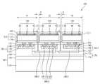
도 1은 제1 실시 예에 따른 발광 소자의 평면도를 나타낸다.
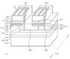
도 2는 도 1에 도시된 발광 소자의 AB 방향의 단면도를 나타낸다.
도 3은 도 1에 도시된 발광 소자를 AB 방향과 CD 방향으로 절단한 사시도를 나타낸다.
도 4는 도 2에 도시된 금속판들의 제1 실시 예를 나타낸다.
도 5는 도 2에 도시된 금속판들의 제2 실시 예를 나타낸다.
도 6은 도 2에 도시된 금속판들의 제3 실시 예를 나타낸다.
도 7은 도 2에 도시된 금속판들의 제4 실시 예를 나타낸다.
도 8은 도 2에 도시된 금속판들의 제5 실시 예를 나타낸다.
도 9는 실시 예에 따른 발광 소자를 포함하는 발광 소자 패키지를 나타낸다.
도 10은 실시 예에 따른 발광 소자 패키지를 포함하는 조명 장치의 분해 사시도이다
도 11은 실시 예에 따른 발광 소자 패키지를 포함하는 표시 장치를 나타낸다.1 is a plan view of a light emitting device according to a first embodiment.
2 is a sectional view of the light emitting device shown in Fig. 1 in the AB direction.
FIG. 3 is a perspective view of the light emitting device shown in FIG. 1 cut along the AB and CD directions.
Fig. 4 shows a first embodiment of the metal plates shown in Fig.
Fig. 5 shows a second embodiment of the metal plates shown in Fig.
6 shows a third embodiment of the metal plates shown in Fig.
Fig. 7 shows a fourth embodiment of the metal plates shown in Fig.
8 shows a fifth embodiment of the metal plates shown in Fig.
9 illustrates a light emitting device package including a light emitting device according to an embodiment.
10 is an exploded perspective view of a lighting device including a light emitting device package according to an embodiment
11 shows a display device including a light emitting device package according to an embodiment.
이하, 실시 예들은 첨부된 도면 및 실시 예들에 대한 설명을 통하여 명백하게 드러나게 될 것이다. 실시 예의 설명에 있어서, 각 층(막), 영역, 패턴 또는 구조물들이 기판, 각 층(막), 영역, 패드 또는 패턴들의 "상/위(on)"에 또는 "하/아래(under)"에 형성되는 것으로 기재되는 경우에 있어, "상/위(on)"와 "하/아래(under)"는 "직접(directly)" 또는 "다른 층을 개재하여 (indirectly)" 형성되는 것을 모두 포함한다. 또한 각 층의 상/위 또는 하/아래에 대한 기준은 도면을 기준으로 설명한다.BRIEF DESCRIPTION OF THE DRAWINGS The above and other features and advantages of the present invention will become more apparent from the following detailed description taken in conjunction with the accompanying drawings, in which: FIG. In the description of the embodiments, it is to be understood that each layer (film), region, pattern or structure may be referred to as being "on" or "under" a substrate, each layer It is to be understood that the terms " on "and " under" include both " directly "or" indirectly " do. In addition, the criteria for the top / bottom or bottom / bottom of each layer are described with reference to the drawings.
도면에서 크기는 설명의 편의 및 명확성을 위하여 과장되거나 생략되거나 또는 개략적으로 도시되었다. 또한 각 구성요소의 크기는 실제크기를 전적으로 반영하는 것은 아니다. 또한 동일한 참조번호는 도면의 설명을 통하여 동일한 요소를 나타낸다. 이하, 첨부된 도면을 참조하여 실시 예에 따른 발광 소자, 그 제조 방법, 및 발광 소자 패키지를 설명한다.In the drawings, dimensions are exaggerated, omitted, or schematically illustrated for convenience and clarity of illustration. Also, the size of each component does not entirely reflect the actual size. The same reference numerals denote the same elements throughout the description of the drawings. Hereinafter, a light emitting device, a method of manufacturing the same, and a light emitting device package according to embodiments will be described with reference to the accompanying drawings.
도 1은 제1 실시 예에 따른 발광 소자(100)의 평면도를 나타내고, 도 2는 도 1에 도시된 발광 소자(100)의 AB 방향의 단면도를 나타낸다.FIG. 1 shows a plan view of a
도 1 및 도 2를 참조하면, 발광 소자(100)는 복수의 발광 영역들(P1 내지 Pn, n>1인 자연수)로 구분되는 발광 구조물(light emitting structure, 110)과, 제1 전극(120)과, 전류 차단층(Current Blocking Layer, 130)과, 보호층(135)과, 오믹층(ohmic layer, 140), 반사층(reflective layer, 150) 및 제1 배리어층(barrier layer, 162)을 포함하는 제1 금속층들(metal layers, 101-1 내지 101-n, n>1인 자연수)과, 제1 절연층(172) 및 제2 절연층(174)을 포함하는 절연층(170)과, 금속판들(metal plates, 180-1 내지 180-j, j≥1인 자연수)과, 제2 배리어층(164), 접합층(bonding layer, 190), 및 지지층(supporter, 195)을 포함하는 제2 금속층(102)과, 패시베이션층(passivation layer, 189)과, 연결 전극(122-1 내지 122-m, m>1인 자연수)을 포함한다.1 and 2, a
발광 구조물(110)은 빛을 발생하며, 복수의 3족 내지 5족 원소의 화합물 반도체층을 포함할 수 있다. 도 2에 도시된 바와 같이, 발광 구조물(110)은 제2 도전형 반도체층(116), 활성층(114), 및 제1 도전형 반도체층(112)이 순차로 적층된 구조일 수 있다. 즉 제2 도전형 반도체층(116)은 제1 도전형 반도체층(112) 아래에 위치할 수 있으며, 활성층(144)은 제1 도전형 반도체층(112)과 제2 도전형 반도체층(114) 사이에 위치할 수 있다.The
제2 도전형 반도체층(116)은 제2 도전형 도펀트가 도핑된 3족-5족 원소의 화합물 반도체일 수 있다. 제2 도전형 반도체층(116)은 InxAlyGa1-x-yN(0≤x≤1, 0≤y≤1, 0≤x+y≤1)의 조성식을 갖는 반도체 재료, 예를 들어 GaN, AlN, AlGaN, InGaN, InN, InAlGaN, AlInN, AlGaAs, GaP, GaAs, GaAsP, AlGaInP 등에서 선택될 수 있으며, Mg, Zn, Ca, Sr, Ba 등의 p형 도펀트가 도핑될 수 있다.The second
활성층(114)은 제1 도전형 반도체층(112) 및 제2 도전형 반도체층(116)으로부터 제공되는 전자(electron)와 정공(hole)의 재결합(recombination) 과정에서 발생하는 에너지에 의해 광을 생성할 수 있다. 활성층(114)은 단일 양자 우물 구조, 다중 양자 우물 구조(MQW), 양자점 구조 또는 양자선 구조 중 어느 하나를 포함할 수 있다.The
예컨대, 활성층(114)이 양자우물구조인 경우, 활성층(114)은 InxAlyGa1-x-yN(0≤x≤1, 0≤y≤1, 0≤x+y≤1)의 조성식을 갖는 우물층과 InaAlbGa1-a-bN(0≤a≤1, 0≤b≤1, 0≤a+b≤1)의 조성식을 갖는 장벽층을 포함하는 단일 또는 다중 양자 우물 구조를 가질 수 있다. 우물층은 장벽층의 에너지 밴드 갭보다 작은 밴드 갭을 갖는 물질로 형성될 수 있다.For example, when the
제1 도전형 반도체층(112)은 제1 도전형 도펀트가 도핑된 3족-5족 원소의 화합물 반도체일 수 있다. 제1 도전형 반도체층(112)은 InxAlyGa1-x-yN(0≤x≤1, 0≤y≤1, 0≤x+y≤1)의 조성식을 갖는 반도체 재료, 예를 들어 GaN, AlN, AlGaN, InGaN, InN, InAlGaN, AlInN, AlGaAs, GaP, GaAs, GaAsP, AlGaInP 등에서 선택될 수 있으며, Si, Ge, Sn, Se, Te 등의 n형 도펀트가 도핑될 수 있다.The first
활성층(114)과 제1 도전형 반도체층(112) 사이, 또는 활성층(114)과 제2 도전형 반도체층(116) 사이에는 도전형 클래드층(clad layer)이 배치될 수도 있으며, 도전형 클래드층은 질화물 반도체(예컨대, AlGaN)로 형성될 수 있다.A conductive clad layer may be disposed between the
발광 구조물(110)은 제2 도전형 반도체층(116) 아래에 제3 도전형 반도체층(미도시)을 더 포함할 수 있으며, 제3 도전형 반도체층은 제2 도전형 반도체층(116)과 반대의 극성을 가질 수 있다. 제1 도전형 반도체층(112)은 N형 반도체층이고, 제2 도전형 반도체층(116)은 P형 반도체층으로 구현될 수 있으며, 이에 따라 발광 구조물(110)은 N-P 접합, P-N 접합, N-P-N 접합, 및 P-N-P 접합 구조 중 적어도 하나를 포함할 수 있다.The
발광 구조물(110)은 복수 개의 서로 이격하는 발광 영역들(P1 내지 Pn, n>1인 자연수) 및 경계 영역(S)을 포함할 수 있다. 이때 경계 영역(S)은 발광 영역들(P1 내지 Pn, n>1인 자연수) 사이에 위치하는 영역일 수 있다. 또는 경계 영역(S)은 발광 영역들(P1 내지 Pn, n>1인 자연수) 각각의 둘레에 위치하는 영역일 수 있다.The
하나의 칩(single chip)의 발광 구조물(110)은 경계 영역(S)에 의하여 복수 개의 발광 영역들(P1 내지 Pn, n>1인 자연수)로 구분될 수 있다.The
보호층(135)은 경계 영역(S) 상에 배치될 수 있으며, 보호층(135)에 의하여 발광 영역들(P1 내지 Pn, n>1인 자연수)이 정의될 수 있다. 보호층(135)은 발광 구조물(110)을 복수의 발광 영역들(P1 내지 Pn, n>1인 자연수)로 구분하기 위한 아이솔레이션(isolation) 식각시 발광 영역들(P1 내지 Pn, n>1인 자연수)을 보호하여 발광 소자(100)의 신뢰성이 저하되는 현상을 감소시킬 수 있다. 보호층(135)은 전류 차단층(130)과 동일한 물질로 형성될 수 있다.The protective layer 135 may be disposed on the boundary region S and the protective layer 135 may define the light emitting regions P1 to Pn and n> 1. The protective layer 135 is formed on the upper surface of the light emitting regions P1 to Pn, n > 1 in the isolation etching for separating the
예컨대, 도 1에 도시된 발광 구조물(110)은 9개의 발광 영역들(P1 내지 Pn, 예컨대, n=9), 및 발광 영역들(P1 내지 Pn, 예컨대, n=9) 사이와 발광 영역들(P1 내지 Pn, 예컨대, n=9) 각각의 둘레에 위치하는 경계 영역(S)으로 구분될 수 있다.For example, the
발광 영역들(P1 내지 Pn, 예컨대, n=9) 각각은 제2 도전형 반도체층(116), 활성층(114), 및 제1 도전형 반도체층(112)이 수직 방향으로 적층된 형태일 수 있다. 여기서 수직 방향은 제2 도전형 반도체층(116)으로부터 제1 도전형 반도체층(112)으로 향하는 방향이거나, 또는 지지층(190)과 수직인 방향일 수 있다.Each of the light emitting regions P1 to Pn (for example, n = 9) may be a stacked structure of the second conductivity
제1 전극(120)은 발광 영역들(P1 내지 Pn, 예컨대, n=9) 상에 배치된다. 즉 제1 전극(120)은 발광 영역들(P1 내지 Pn, 예컨대, n=9) 각각의 제1 도전형 반도체층(112) 상에 배치될 수 있다. 제1 전극(120)은 소정의 패턴 형상일 수 있으며, 도 1에 도시된 패턴에 한정되는 것은 아니며, 다양한 형태로 구현될 수 있다.The
제1 도전형 반도체층(112)의 상면은 광 추출 효율을 증가시키기 위해 거칠기(roughness, 112-1)가 형성될 수 있다. 또한 광 추출 효율을 증가시키기 위하여 제1 전극(120)의 표면에도 거칠기(미도시)가 형성될 수 있다.The upper surface of the first conductivity
제1 전극(120)은 발광 영역들(P1 내지 Pn, 예컨대, n=9) 각각의 제1 도전형 반도체층(112)의 상면 가장 자리를 따라 배치되는 외부 전극(92), 및 외부 전극(92)의 내부에 배치되는 내부 전극(94)을 포함할 수 있다.The
전류 차단층(130)은 발광 영역들(P1 내지 Pn, 예컨대, n=9) 각각의 제2 도전형 반도체층(116) 아래에 배치되며, 제2 도전형 반도체층(116)의 하면에 접촉할 수 있다.The
예컨대, 전류 차단층(130)은 발광 영역들(P1 내지 Pn, 예컨대, n=9) 각각의 제2 도전형 반도체층(116) 하면의 일부 영역 상에 배치될 수 있다. 전류 차단층(130)은 발광 영역들(P1 내지 Pn, 예컨대, n=9) 각각의 특정 영역에 전류가 집중되는 현상을 완화하여 발광 소자(100)의 발광 효율을 향상시킬 수 있다.For example, the
전류 차단층(130)은 제1 전극(120)에 대응하여 배치되며, 수직 방향으로 제1 전극(120)과 적어도 일부가 오버랩된다. 전류 차단층(130)은 제1 전극(120)의 패턴에 대응하는 패턴 형상을 가질 수 있다. 여기서 수직 방향은 제2 도전형 반도체층(112)으로부터 제1 도전형 반도체층(116)으로 향하는 방향일 수 있다.The
전류 차단층(130)은 반사층(150) 또는 오믹층(140)보다 전기 전도성이 낮은 물질, 제2 도전형 반도체층(116)과 쇼트키 접촉을 형성하는 물질, 또는 전기 절연성 물질을 이용하여 형성될 수 있다. 예를 들어, 전류 차단층(130)은 ZnO, SiO2, SiON,Si3N4, Al2O3 ,TiO2, Ti, Al, Cr 중 적어도 하나를 포함할 수 있다.The
제1 금속층들(101-1 내지 101-n, 예컨대, n=9) 각각은 복수의 발광 영역들(P1 내지 Pn, 예컨대,n=9) 중 대응하는 어느 하나의 제2 도전형 반도체층(116) 아래에 서로 이격하여 배치될 수 있다. 제1 금속층들(101-1 내지 101-n, 예컨대, n=9) 각각은 오믹층(140), 반사층(150), 및 제1 배리어층(162)을 포함할 수 있다.Each of the first metal layers 101-1 to 101-n, for example, n = 9 may be formed of a corresponding one of the plurality of light emitting regions P1 to Pn, for example, n = 9, 116, respectively. Each of the first metal layers 101-1 through 101-n, e.g., n = 9, may include an
오믹층(140)은 발광 영역들(P1 내지 Pn, 예컨대, n=9) 각각의 아래에 배치되며, 제2 도전형 반도체층(116)과 오믹 접촉한다. 오믹층(140)은 제2 전극층(101)으로부터 발광 구조물(240)로 전원이 원활히 공급되도록 하는 역할을 한다. 예컨대, 오믹층(140)은 In, Zn, Ag, Sn, Ni, 및 Pt 중 적어도 하나를 포함할 수 있다.The
반사층(150)은 발광 영역들(P1 내지 Pn, 예컨대, n=9) 각각의 오믹층(140) 아래에 배치되며, 발광 구조물(110)로부터 입사되는 광을 반사시켜 발광 소자(100)의 광 추출 효율을 향상시킬 수 있다. 반사층(150)은 오믹층(140)의 최외각 측면과 접하며, 오믹층(140)의 둘레를 감쌀 수 있다.The
반사층(150)은 Ag, Ni, Al, Rh, Pd, Ir, Ru, Mg, Zn, Pt, Au, Hf 중 적어도 하나를 포함하는 금속 또는 이들의 합금으로 형성될 수 있다. 또한 반사층(150)은 금속 또는 합금과 IZO(indium zinc oxide), IZTO(indium zinc tin oxide), IAZO(indium aluminum zinc oxide), IGZO(indium gallium zinc oxide), IGTO(indium gallium tin oxide), AZO(aluminum zinc oxide), ATO(antimony tin oxide) 등의 투광성 전도성 물질을 이용하여 다층으로 형성할 수 있다. 예를 들어, 반사층(150)은 IZO/Ni, AZO/Ag, IZO/Ag/Ni, AZO/Ag/Ni 등으로 형성할 수 있다.The
다른 실시 예에서는 오믹층(140)을 따로 형성하지 않고, 반사층(150)으로 사용되는 물질을 제2 도전형 반도체층(116)과 오믹 접촉을 하는 물질로 선택하여 반사층(150)이 제2 도전형 반도체층(116)과 오믹 접촉을 이루도록 할 수 있다.The
제1 배리어층(162)은 발광 영역들(P1 내지 Pn, 예컨대,n=9) 각각의 반사층(150) 아래에 배치되며, 지지층(195)의 금속 이온이 반사층(150)과 오믹층(140)으로 전달 또는 확산하는 것을 방지한다. 제1 배리어층(162)은 배리어 금속 물질, 예컨대, Pt, Ti, W, V, Fe, Mo 중 적어도 하나를 포함하며, 단일층(single layer) 또는 멀티층(multilayer)일 수 있다.The
금속판들(180-1 내지 180-j, j≥1인 자연수)은 제1 금속층들(101-1 내지 101-n, 예컨대, n=9) 아래에 서로 이격하여 배치된다. 금속판들(180-1 내지 180-j, j≥1인 자연수)은 도전 물질, 예컨대, Ti, Ni, Cu, Au, Pt, W 중 적어도 하나 또는 이들의 합금일 수 있다.The metal plates 180-1 through 180-j, where j is a natural number, are disposed apart from each other under the first metal layers 101-1 through 101-n, for example, n = 9. The metal plates 180-1 through 180-j, where j is a natural number, may be a conductive material, for example, at least one of Ti, Ni, Cu, Au, Pt and W or an alloy thereof.
금속판들(180-1 내지 180-j, j≥1인 자연수) 각각은 발광 영역들(P1 내지 Pn, 예컨대, n=9) 중 어느 하나를 제외한 나머지 발광 영역들(P2 내지 Pn, 예컨대, n=9) 각각에 대응하여 배치될 수 있다.Each of the metal plates 180-1 through 180-j, where j is a natural number, is the sum of the remaining light emitting regions P2 through Pn except for one of the light emitting regions P1 through Pn, = 9), respectively.
예컨대, 금속판들(180-1 내지 180-j, 예컨대, j=8) 각각은 제1 금속층들(101-1 내지 101-n, 예컨대,n=9) 중 어느 하나를 제외한 나머지들 각각에 대응하여 배치될 수 있으며, 대응하는 어느 하나와 전기적으로 연결될 수 있다.For example, each of the metal plates 180-1 to 180-j (e.g., j = 8) corresponds to each of the remainders except one of the first metal layers 101-1 to 101-n, e.g., n = And can be electrically connected to any corresponding one of them.
금속판들(180-1 내지 180-j, 예컨대, j=8) 각각은 제1 발광 영역(P1)을 제외한 나머지 발광 영역들(P2 내지 Pn, 예컨대, n=9) 각각의 아래에 위치하는 제1 금속층들(101-2 내지 101-n, 예컨대, n=9)에 대응하여 배치될 수 있다.Each of the metal plates 180-1 to 180-j, for example, j = 8 is formed of a metal material such as a metal oxide or the like, which is located under each of the remaining light emitting regions P2 to Pn (e.g., n = 9) except for the first light emitting region P1 1 metal layers 101-2 to 101-n, e.g., n = 9.
예컨대, 제1 금속판(180-1)은 제2 발광 영역(P2)의 제1 금속층(101-2)에 대응하여 배치될 수 있으며, 제2 발광 영역(P2)의 제1 금속층(101-2)과 전기적으로 연결될 수 있다.For example, the first metal plate 180-1 may be disposed corresponding to the first metal layer 101-2 of the second light emitting region P2, and the first metal layer 101-2 As shown in FIG.
제1 절연층(172)은 제1 금속층들(101-1 내지 101-n, 예컨대, n=9)의 둘레를 감싼다. 제1 절연층(172)은 제1 금속층들(101-1 내지 101-n, 예컨대, n=9) 사이, 및 제1 금속층들(101-1 내지 101-n, 예컨대, n=9)과 금속판들(180-1 내지 180-j, 예컨대, j=8) 사이에 배치될 수 있다.The first insulating
제1 절연층(172)은 제1 금속층들(101-1 내지 101-n, 예컨대, n=9) 상호 간을 전기적으로 절연하고, 제1 금속층들(101-1 내지 101-n, 예컨대, n=9)과 금속판들(180-1 내지 180-j, 예컨대, j=8) 상호 간을 서로 전기적으로 절연시킬 수 있다.The first insulating
제2 배리어층(164)은 제1 절연층(172) 아래에 배치되며, 발광 영역들(P1 내지 Pn, 예컨대, n=9) 중 어느 하나의 아래에 위치하는 제1 금속층(예컨대, 101-1)과 전기적으로 연결될 수 있다.The
예컨대, 제2 배리어층(164)은 제2 절연층(174) 아래에 위치하며, 제1 발광 영역(P1) 아래에 위치하는 제1 금속층(101-1)과 전기적으로 접촉할 수 있다.For example, the
후술하는 지지층(195)과 본딩되는 제2 배리어층(164)과 전기적으로 연결되는 제1 발광 영역(P1)의 제1 금속층(예컨대, 101-1)에는 제2 전원(예컨대, 양의 전원)이 공급될 수 있다.A second power source (for example, a positive power source) is connected to the first metal layer (for example, 101-1) of the first light emitting region P1, which is electrically connected to the
제2 배리어층(164)은 제1 배리어층(162)과 동일한 물질로 이루어질 수 있으며, 단일층(single layer) 또는 멀티층(multilayer)일 수 있다.The
제2 절연층(174)은 금속판들(180-1 내지 180-j, 예컨대, j=8) 사이, 및 금속판들(180-1 내지 180-j, 예컨대, j=8)과 제2 배리어층(164) 사이에 배치될 수 있다. 제1 절연층(172) 및 제2 절연층(174)은 절연 물질, 예컨대, Al2O3, SiO2,Si3N4, TiO2, AlN 중 적어도 하나일 수 있으며, 단층 또는 다층일 수 있다.The second
금속판들(180-1 내지 180-j, 예컨대, j=8) 각각은 적어도 일부가 제1 절연층(172)을 관통하여 금속판들(180-1 내지 180-j, 예컨대, j=8) 각각에 대응하는 제1 금속층(101-2 내지 101-n, 예컨대, n=9)과 접촉할 수 있다.Each of the metal plates 180-1 through 180-j, for example, j = 8, at least partially penetrates the first insulating
예컨대, 금속판들(180-1 내지 180-j, 예컨대, j=8) 각각은 적어도 일부가 제1 절연층(172)을 관통하여 제1 배리어층(162)과 접촉할 수 있다.For example, each of the metal plates 180-1 through 180-j, e.g., j = 8, may at least partially contact the
금속판들(180-1 내지 180-j, 예컨대, j=8) 각각은 발광 영역들(P1 내지 Pn, 예컨대, n=9) 중 어느 하나(예컨대, P1)를 제외한 나머지 발광 영역들(P2 내지 Pn, 예컨대, n=9)의 제1 금속층(101-2 내지 101-n, 예컨대, n=9)에 대응하여 배치될 수 있다.Each of the metal plates 180-1 to 180-j, for example, j = 8 is formed in the other light emitting regions P2 to Pn except for any one of the light emitting regions P1 to Pn, N = 9) of the first metal layer 101-2 to 101-n (e.g., Pn, e.g., n = 9).
나머지 발광 영역들(P2 내지 Pn, 예컨대, n=9) 각각에 대응하여 배치되는 금속판들(180-1 내지 180-j, 예컨대, j=8)의 일 부분은 인접하는 경계 영역(S)과 수직 방향으로 오버랩될 수 있다. 예컨대, 제2 발광 영역(P2)에 대응하여 배치되는 제1 금속판(180-1)은 제2 발광 영역(P2)에 인접하는 경계 영역(S)과 수직 방향으로 오버랩되도록 확장될 수 있다.A part of the metal plates 180-1 to 180-j (for example, j = 8) arranged corresponding to each of the remaining light emitting areas P2 to Pn, for example, n = It can be overlapped in the vertical direction. For example, the first metal plate 180-1 disposed corresponding to the second light emitting region P2 may be extended so as to overlap with the boundary region S adjacent to the second light emitting region P2 in the vertical direction.
또한 나머지 발광 영역들(P2 내지 Pn, 예컨대, n=9) 중 어느 하나의 발광 영역(예컨대, P2)에 대응하여 배치되는 금속판(예컨대, 180-1)의 적어도 일 부분은 상기 어느 하나의 발광 영역(예컨대, P2)에 인접하는 다른 발광 영역(예컨대, P1)과 수직 방향으로 오버랩될 수 있다. 여기서 수직 방향은 금속판들(180-1 내지 180-n, 예컨대, n=9)로부터 발광 영역들(101-1 내지 101-n, 예컨대, n=9)로 향하는 방향이거나, 또는 금속판들(180-1 내지 180-j, 예컨대, j=8)에 수직인 상부 방향일 수 있다.At least a part of the metal plate (for example, 180-1) arranged corresponding to any one of the light emitting regions (for example, P2) of the remaining light emitting regions (P2 to Pn, (E.g., P1) adjacent to the region (e.g., P2). Here, the vertical direction is the direction from the metal plates 180-1 to 180-n, e.g., n = 9, to the light emitting regions 101-1 to 101-n, e.g., n = 9, -1 to 180-j, e.g., j = 8).
지지층(195)은 제2 배리어층(164) 아래에 배치되며, 발광 구조물(110)을 지지하고 제1 전극(120)과 함께 발광 구조물(110)에 전원을 제공한다. 지지층(190)은 전도성이며, 예를 들어, 구리(Cu), 금(Au), 니켈(Ni), 몰리브덴(Mo), 구리-텅스텐(Cu-W)와 같은 금속 물질 또는 Si, Ge, GaAs, ZnO, SiC, 및 SiGe 중 적어도 하나를 포함하는 반도체 물질일 수 있다.A
접합층(190)은 제2 배리어층(164)과 지지층(195) 사이에 배치된다. 접합층(190)은 제2 배리어층(164)과 지지층(195) 사이에 삽입되어 양자를 접합할 수 있다. 접합층(190)은 지지층(195)을 본딩 방식으로 접합하기 위해 형성되는 것이기 때문에, 지지층(195)을 도금이나 증착 방법으로 형성하는 경우 또는 지지층(195)이 반도체층일 경우에는 접합층(190)은 생략될 수 있다. 접합층(190)은 Au, Sn, Ni, Nb, In, Cu, Ag 및 Pd 중 적어도 하나를 포함할 수 있다.The
패시베이션층(185)은 발광 영역들(P1 내지 Pn, 예컨대, n=9) 각각의 측면 및/또는 상면 상에 배치될 수 있다. 예컨대, 패시베이션층(185)은 발광 영역들(P1 내지 Pn, 예컨대, n=9) 각각에 속하는 제1 도전형 반도체층(112)의 측면, 활성층(114)의 측면, 및 제2 도전형 반도체층(116)의 측면 상에 배치될 수 있으며, 또한 패시베이션층(185)은 발광 영역들(P1 내지 Pn, 예컨대,n=9) 각각의 제1 도전형 반도체층(112)의 상면 상에 배치될 수 있다. 제1 전극(120)은 패시베이션층(185)으로부터 노출될 수 있다.The
연결 전극(122-1 내지 122-m, m>1인 자연수)은 인접하는 2개의 발광 영역들 중 어느 하나의 제1 도전형 반도체층(112) 상에 배치되는 제1 전극(120)과 나머지 다른 하나의 제1 금속층에 대응하여 배치되는 금속판을 전기적으로 연결한다.The connection electrodes 122-1 to 122-m and m> 1 are formed of a
예컨대, 제1 연결 전극(122-1)은 제1 발광 영역(P1)의 제1 전극(120)과 제2 발광 영역(P2)의 제1 금속층(101-2)에 대응하는 제1 금속판(180-1)을 전기적으로 연결할 수 있다.For example, the first connection electrode 122-1 is electrically connected to the
연결 전극(122-1 내지 122-m, m>1인 자연수)은 패시베이션층(185) 상에 배치될 수 있으며, 보호층(135) 및 제1 절연층(172)을 관통하여 인접하는 발광 영역들 중 어느 하나의 제1 전극(120)과 나머지 다른 하나의 금속판(180-1 내지 180-j 중 어느 하나, 예컨대, j=8)을 전기적으로 연결될 수 있다.The connection electrodes 122-1 to 122-m and m> 1 are disposed on the
연결 전극(122-1 내지 122-m, m>1인 자연수) 및 금속판들(180-1 내지 180-j)에 의하여 발광 영역들(P1 내지 Pn, 예컨대, n=9)은 서로 직렬 연결될 수 있다.The light emitting regions P1 to Pn, e.g., n = 9, can be connected in series by the connection electrodes 122-1 to 122-m, m> 1 and the metal plates 180-1 to 180- have.
그리고 직렬 연결되는 발광 영역들(P1 내지 pN, 예컨대, n=9) 중 어느 하나(예컨대, P9)의 제1 전극(120)은 패드부(121a, 121b)를 더 포함할 수 있다. 패드부(121a, 121b)는 제1 전원(예컨대, 음(-)의 전원)을 공급하기 위하여 와이어(wire)가 본딩되는 영역일 수 있다.The
도 3은 도 1에 도시된 발광 소자(100)를 AB 방향과 CD 방향으로 절단한 사시도를 나타내며, 도 4는 도 2에 도시된 금속판들(180-1 내지 180-j, j≥1)의 제1 실시 예(181)를 나타낸다.FIG. 3 is a perspective view of the
도 3 및 도 4를 참조하면, 금속판들(180-1 내지 180-j, 예컨대, j=8) 각각은 베이스 판(base plate, 401) 및 관통부(402)를 포함한다.3 and 4, each of the metal plates 180-1 to 180-j, for example, j = 8 includes a
베이스 판(401)은 일정한 면적(세로(L1)×가로(L2)) 및 두께(t)를 갖는 판 (plate) 형태이며, 제1 금속층들(101) 아래에 배치된다. 도 4에서 베이스 판(401)은 사각형 형상이지만, 실시 예가 이에 한정되는 것은 아니며, 베이스 판(401)은 원형, 타원형, 또는 다각형 등과 같이 다양한 형상을 가질 수 있다.The
베이스 판(401)은 제1 발광 영역(P1)을 제외한 나머지 발광 영역들(P2 내지 Pn, 예컨대, n=9)에 대응하여 제1 절연층(172) 및 제2 절연층(174) 사이에 배치되며, 베이스 판(401)의 일 영역에 연결 전극(122-1 내지 122-m, m>1인 자연수)이 전기적으로 연결될 수 있다.The
나머지 발광 영역들(P2 내지 Pn, 예컨대, n=9) 중 어느 하나의 발광 영역(예컨대, P2)에 대응하여 배치되는 베이스 판(401)의 적어도 일 부분은 인접하는 경계 영역(S) 및 인접하는 다른 발광 영역(예컨대, P1)과 수직 방향으로 오버랩될 수 있다. 예컨대, 제2 발광 영역(P2)에 대응하여 배치되는 베이스 판(401)의 적어도 일 부분은 인접하는 경계 영역(S) 및 제1 발광 영역(P1)과 수직 방향으로 오버랩될 수 있다.At least a part of the
나머지 발광 영역들(P2 내지 Pn, 예컨대, n=9) 중 어느 하나의 발광 영역(예컨대, P3)에 대응하여 배치되는 베이스 판(180)의 적어도 일 부분은 인접하는 경계 영역(S) 및 인접하는 다른 발광 영역(예컨대, P2)과 수직 방향으로 오버랩될 수 있다.At least a part of the base plate 180 disposed corresponding to one of the light emission regions (for example, P3) of the remaining light emission regions (P2 to Pn, e.g., n = 9) (For example, P2) which is different from the light emitting region (e.g.
관통부(402)는 베이스 판(401)의 일 영역과 연결되고, 베이스 판(104)으로부터 돌출된다. 관통부(402)는 제1 절연층(172)을 관통하여 대응하는 제1 금속층과 연결될 수 있다. 예컨대, 관통부(402)는 제1 절연층(172)을 관통하여 제1 배리어층(162)과 연결될 수 있다.The penetrating
관통부(402)는 베이스 판(401)과 동일한 물질이며, 베이스 판(401)과 일체형일 수 있다. 관통부(402)는 돌기 형태이며, 가로 및 세로의 길이가 금속판(401)의 가로의 길이(L2) 및 세로의 길이(L1)보다 작다.The penetrating
또한 도 4에서 관통부(402)는 베이스 판(401)의 일 측면에 접하여 배치되지만, 실시 예가 이에 한정되는 것은 아니며, 베이스 판(401)의 상면의 어느 한 부분에 배치될 수 있다.4, the through-
도 5는 도 2에 도시된 금속판들(180-1 내지 180-j, j≥1)의 제2 실시 예(182)를 나타낸다. 도 4과 동일한 도면 부호는 동일한 구성을 나타내며, 앞에서 설명한 내용과 중복되는 내용은 생략하거나 간략히 설명한다.Fig. 5 shows a
도 5를 참조하면, 금속판들(180-1 내지 180-j, j≥1) 각각은 베이스 판(401) 및 관통부(402-1)을 포함한다, 관통부(402-1)는 돌기 형태이며, 일변의 길이(예컨대, 세로의 길이(K)가 베이스 판(401)의 일변의 길이(예컨대, 세로의 길이(L1))와 동일할 수 있다(K=L1).5, each of the metal plates 180-1 to 180-j, j? 1 includes a
도 6은 도 2에 도시된 금속판들(180-1 내지 180-j, j≥1)의 제3 실시 예(183)를 나타낸다. 도 4과 동일한 도면 부호는 동일한 구성을 나타내며, 앞에서 설명한 내용과 중복되는 내용은 생략하거나 간략히 설명한다.Fig. 6 shows a
도 6을 참조하면, 금속판들(180-1 내지 180-j, j≥1) 각각은 베이스 판(501) 및 관통부(402)를 포함한다. 베이스 판(501)은 적어도 하나의 관통 홈(502)이 형성될 수 있다. 관통부(402)는 적어도 하나의 관통 홈(502)과 이격하여 배치될 수 있다.6, each of the metal plates 180-1 to 180-j, j? 1 includes a
적어도 하나의 관통 홈(502)에는 제2 절연층(174)이 채워질 수 있으며, 제2 절연층(174)은 적어도 하나의 관통 홈(502)을 통하여 제1 절연층(172)과 접촉할 수 있다. 적어도 하나의 관통 홈(502)은 제1 절연층(172)과 제2 절연층(174) 사이의 접착력(adhesion)을 향상시킬 수 있다.The at least one through-
도 6에서 관통 홈(502)은 원형이나, 실시 예는 이에 한정되는 것은 아니며, 관통 홈(502)은 원형, 타원형, 또는 다각형 등과 같이 다양한 형태일 수 있다.6, the through-
도 7은 도 2에 도시된 금속판들(180-1 내지 180-j, j≥1)의 제4 실시 예(184)를 나타낸다. 도 4과 동일한 도면 부호는 동일한 구성을 나타내며, 앞에서 설명한 내용과 중복되는 내용은 생략하거나 간략히 설명한다.Fig. 7 shows a
도 7을 참조하면, 금속판들(180-1 내지 180-j, j≥1) 각각은 베이스 판(601) 및 관통부(402)를 포함한다. 베이스 판(601)의 상면 및 하면 중 적어도 하나에는 거칠기(roughness, 602)가 형성될 수 있다. 이때 거칠기(602)는 규칙적인 요철이거나, 불규칙적인 요철일 수 있다. 거칠기(602)는 금속판들(180-1 내지 180-j, j≥1)과 제1 절연층(172) 사이의 접착력 또는/및 금속판들(180-1 내지 180-j, j≥1)과 제2 절연층(174) 사이의 접착력을 향상시킬 수 있다.Referring to Fig. 7, each of the metal plates 180-1 to 180-j, j? 1 includes a
도 8은 도 2에 도시된 금속판들(180-1 내지 180-j, j≥1)의 제5 실시 예(185)를 나타낸다. 도 5를 참조하면, 금속판들(180-1 내지 180-j, j≥1) 각각은 그물 구조(meshed structure)를 갖는 베이스 판(701) 및 베이스판(701)의 일 영역과 연결되고, 제1 절연층(172)을 관통하여 제1 금속층(101)(예컨대, 제1 배리어층(162))과 접촉하는 관통부(702)를 포함한다.Fig. 8 shows a
일반적으로 직렬 연결되는 복수의 발광 영역들을 포함하는 발광 구조물에 높은 구동 전압을 갖는 전원이 인가되는 경우, 전원이 직접 인가되는 발광 영역 및 이와 인접한 발광 영역에 가장 큰 전기장이 집중되고, 전기장이 집중된 발광 영역들은 파손될 수 있다.In general, when a power source having a high driving voltage is applied to a light emitting structure including a plurality of light emitting regions connected in series, the largest electric field is concentrated in the light emitting region to which the power is directly applied and the light emitting region adjacent thereto, Areas may be destroyed.
실시 예는 제2 금속층(102), 제2 배리어층(164), 제1 금속층(101-1)을 통하여 발광 구조물(110)에 제2 전원(예컨대, 양(+)의 전원)이 공급되며, 제9 발광 영역(P9)의 제1 전극(120) 및 패드부(121a, 121b)를 통하여 발광 구조물(110)에 제1 전원(예컨대, 음(-)의 전원)이 공급될 수 있다. 그리고 발광 영역들(P1 내지 Pn, 예컨대, n=9) 각각은 연결 전극(122-1 내지 122-m, 예컨대, m=8) 및 금속판들(180-1 내지 180-j, 예컨대, j=8)에 의하여 서로 직렬 연결될 수 있다.The second power source (for example, a positive power source) is supplied to the
발광 구조물(110)에 높은 구동 전압이 인가되는 경우, 실시 예는 발광 영역들 사이를 직렬 연결하는 금속판들(180-1 내지 180-j, j≥1)에 의하여 제1 발광 영역(P1) 및 제2 발광 영역(P2)에 집중되는 전기장(electric field)을 분산시킴으로써 발광 소자(100)가 파괴되는 것을 방지할 수 있다.In the case where a high driving voltage is applied to the
도 9는 실시 예에 따른 발광 소자를 포함하는 발광 소자 패키지를 나타낸다.9 illustrates a light emitting device package including a light emitting device according to an embodiment.
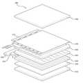
도 9를 참조하면, 실시 예에 따른 발광 소자 패키지는 패키지 몸체(610), 제1 리드 프레임(612), 제2 리드 프레임(614), 발광 소자(620), 반사판(625), 와이어(630), 및 봉지층(640)을 포함한다.9, the light emitting device package according to the embodiment includes a
패키지 몸체(610)는 일측 영역에 캐버티(cavity)가 형성된 구조이다. 이때 캐버티의 측벽은 경사지게 형성될 수 있다. 패키지 몸체(610)는 실리콘 기반의 웨이퍼 레벨 패키지(wafer level package), 실리콘 기판, 실리콘 카바이드(SiC), 질화알루미늄(aluminum nitride, AlN) 등과 같이 절연성 또는 열전도도가 좋은 기판으로 형성될 수 있으며, 복수 개의 기판이 적층되는 구조일 수 있다. 실시 예는 상술한 몸체의 재질, 구조, 및 형상으로 한정되지 않는다.The
제1 리드 프레임(612) 및 제2 리드 프레임(614)은 열 배출이나 발광 소자의 장착을 고려하여 서로 전기적으로 분리되도록 패키지 몸체(610)의 표면에 배치될 수 있다. 발광 소자(620)는 제1 리드 프레임(612) 및 제2 리드 프레임(614)과 전기적으로 연결된다. 이때 발광 소자(620)는 실시 예에 따른 발광 소자(100)일 수 있다.The
예컨대, 도 2에 도시된 발광 소자(100)의 제2 금속층(102)은 제2 리드 프레임(614)에 전기적으로 연결되고, 와이어(630)에 의하여 제9 발광 영역(P9)의 패드부(121a, 121b)는 제1 리드 프레임(612)에 본딩될 수 있다.For example, the
반사판(625)은 발광 소자(620)에서 방출된 빛을 소정의 방향으로 지향하도록 패키지 몸체(610)의 캐버티 측벽에 형성된다. 반사판(625)은 광반사 물질로 이루어지며, 예컨대, 금속 코팅이거나 금속 박편일 수 있다.The
봉지층(640)은 패키지 몸체(610)의 캐버티 내에 위치하는 발광 소자(620)를 포위하여 발광 소자(620)를 외부 환경으로부터 보호한다. 봉지층(640)은 에폭시 또는 실리콘과 같은 무색 투명한 고분자 수지 재질로 이루어진다. 봉지층(640)은 발광 소자(620)에서 방출된 광의 파장을 변화시킬 수 있도록 형광체가 포함될 수 있다. 발광 소자 패키지는 상기에 개시된 실시 예들의 발광 소자들 중 적어도 하나를 탑재할 수 있으며, 이에 대해 한정하지는 않는다.The
실시 예에 따른 발광 소자 패키지는 복수 개가 기판 상에 어레이되며, 발광 소자 패키지의 광 경로 상에 광학 부재인 도광판, 프리즘 시트, 확산 시트 등이 배치될 수 있다. 이러한 발광 소자 패키지, 기판, 광학 부재는 백라이트 유닛으로 기능할 수 있다.A plurality of light emitting device packages according to embodiments may be arranged on a substrate, and a light guide plate, a prism sheet, a diffusion sheet, and the like may be disposed on the light path of the light emitting device package. The light emitting device package, the substrate, and the optical member may function as a backlight unit.
또 다른 실시 예는 상술한 실시 예들에 기재된 발광 소자 또는 발광 소자 패키지를 포함하는 표시 장치, 지시 장치, 조명 시스템으로 구현될 수 있으며, 예를 들어, 조명 시스템은 램프, 가로등을 포함할 수 있다.Still another embodiment may be implemented as a display device, an indicating device, and a lighting system including the light emitting device or the light emitting device package described in the above embodiments. For example, the lighting system may include a lamp and a streetlight.
도 10은 실시 예에 따른 발광 소자 패키지를 포함하는 조명 장치의 분해 사시도이다. 도 10을 참조하면, 조명 장치는 광을 투사하는 광원(750)과 광원(7500)이 내장되는 하우징(700)과 광원(750)의 열을 방출하는 방열부(740) 및 광원(750)과 방열부(740)를 하우징(700)에 결합하는 홀더(760)를 포함한다.10 is an exploded perspective view of a lighting device including a light emitting device package according to an embodiment. 10, the illumination device includes a
하우징(700)은 전기 소켓(미도시)에 결합되는 소켓 결합부(710)와, 소켓 결합부(710)와 연결되고 광원(750)이 내장되는 몸체부(730)를 포함한다. 몸체부(730)에는 하나의 공기 유동구(720)가 관통하여 형성될 수 있다.The
하우징(700)의 몸체부(730) 상에 복수 개의 공기 유동구(720)가 구비되며, 공기 유동구(720)는 하나이거나, 복수 개일 수 있다. 공기 유동구(720)는 몸체부(730)에 방사상으로 배치되거나 다양한 형태로 배치될 수 있다.A plurality of air flow holes 720 are provided on the
광원(750)은 기판(754) 상에 구비되는 복수 개의 발광 소자 패키지(752)를 포함한다. 기판(754)은 하우징(700)의 개구부에 삽입될 수 있는 형상일 수 있으며, 후술하는 바와 같이 방열부(740)로 열을 전달하기 위하여 열전도율이 높은 물질로 이루어질 수 있다. 복수 개의 발광 소자 패키지는 상술한 실시 예일 수 있다.The
광원(750)의 하부에는 홀더(760)가 구비되며, 홀더(760)는 프레임 및 다른 공기 유동구를 포함할 수 있다. 또한, 도시되지는 않았으나 광원(750)의 하부에는 광학 부재가 구비되어 광원(750)의 발광 소자 패키지(752)에서 투사되는 빛을 확산, 산란 또는 수렴시킬 수 있다.A
도 11은 실시 예에 따른 발광 소자 패키지를 포함하는 표시 장치를 나타낸다.11 shows a display device including a light emitting device package according to an embodiment.
도 11을 참조하면, 표시 장치(800)는 바텀 커버(810)와, 바텀 커버(810) 상에 배치되는 반사판(820)과, 광을 방출하는 발광 모듈(830, 835)과, 반사판(820)의 전방에 배치되며 상기 발광 모듈(830,835)에서 발산되는 빛을 표시 장치 전방으로 안내하는 도광판(840)과, 도광판(840)의 전방에 배치되는 프리즘 시트들(850,860)을 포함하는 광학 시트와, 광학 시트 전방에 배치되는 디스플레이 패널(870)과, 디스플레이 패널(870)과 연결되고 디스플레이 패널(870)에 화상 신호를 공급하는 화상 신호 출력 회로(872)와, 디스플레이 패널(870)의 전방에 배치되는 컬러 필터(880)를 포함할 수 있다. 여기서 바텀 커버(810), 반사판(820), 발광 모듈(830,835), 도광판(840), 및 광학 시트는 백라이트 유닛(Backlight Unit)을 이룰 수 있다.11, the
발광 모듈은 기판(830) 상의 발광 소자 패키지(835)를 포함하여 이루어진다. 여기서, 기판(830)은 PCB 등이 사용될 수 있다. 발광 소자 패키지(835)는 실시 예에 따른 발광 소자 패키지일 수 있다.The light emitting module comprises a light emitting
바텀 커버(810)는 표시 장치(800) 내의 구성 요소들을 수납할 수 있다. 그리고, 반사판(820)은 본 도면처럼 별도의 구성요소로 마련될 수도 있으며, 도광판(840)의 후면이나, 바텀 커버(810)의 전면에 반사도가 높은 물질로 코팅되는 형태로 마련되는 것도 가능하다.The
여기서, 반사판(820)은 반사율이 높고 초박형으로 사용 가능한 소재를 사용할 수 있고, 폴리에틸렌 테레프탈레이트(PolyEthylene Terephtalate; PET)를 사용할 수 있다.Here, the
그리고, 도광판(830)은 폴리메틸메타크릴레이트(PolyMethylMethAcrylate; PMMA), 폴리카보네이트(PolyCarbonate; PC), 또는 폴리에틸렌(PolyEthylene; PE) 등으로 형성될 수 있다.The
그리고, 제1 프리즘 시트(850)는 지지 필름의 일면에, 투광성이면서 탄성을 갖는 중합체 재료로 형성될 수 있으며, 중합체는 복수 개의 입체구조가 반복적으로 형성된 프리즘층을 가질 수 있다. 여기서, 복수 개의 패턴은 도시된 바와 같이 마루와 골이 반복적으로 스트라이프 타입으로 구비될 수 있다.The
그리고, 제2 프리즘 시트(860)에서 지지 필름 일면의 마루와 골의 방향은, 제1 프리즘 시트(850) 내의 지지필름 일면의 마루와 골의 방향과 수직할 수 있다. 이는 발광 모듈과 반사 시트로부터 전달된 빛을 디스플레이 패널(1870)의 전면으로 고르게 분산하기 위함이다.In the
그리고, 도시되지는 않았으나, 도광판(840)과 제1 프리즘 시트(850) 사이에 확산 시트가 배치될 수 있다. 확산 시트는 폴리에스터와 폴리카보네이트 계열의 재료로 이루어질 수 있으며, 백라이트 유닛으로부터 입사된 빛을 굴절과 산란을 통하여 광 투사각을 최대로 넓힐 수 있다. 그리고, 확산 시트는 광확산제를 포함하는 지지층과, 광출사면(제1 프리즘 시트 방향)과 광입사면(반사시트 방향)에 형성되며 광확산제를 포함하지 않는 제1 레이어와 제2 레이어를 포함할 수 있다.Although not shown, a diffusion sheet may be disposed between the
실시 예에서 확산 시트, 제1 프리즘시트(850), 및 제2 프리즘시트(1860)가 광학 시트를 이루는데, 광학 시트는 다른 조합 예를 들어, 마이크로 렌즈 어레이로 이루어지거나 확산 시트와 마이크로 렌즈 어레이의 조합 또는 하나의 프리즘 시트와 마이크로 렌즈 어레이의 조합 등으로 이루어질 수 있다.In an embodiment, the diffusion sheet, the
디스플레이 패널(870)은 액정 표시 패널(Liquid crystal display)가 배치될 수 있는데, 액정 표시 패널(860) 외에 광원을 필요로 하는 다른 종류의 표시 장치가 구비될 수 있다.The
이상에서 실시 예들에 설명된 특징, 구조, 효과 등은 본 발명의 적어도 하나의 실시 예에 포함되며, 반드시 하나의 실시 예에만 한정되는 것은 아니다. 나아가, 각 실시 예에서 예시된 특징, 구조, 효과 등은 실시 예들이 속하는 분야의 통상의 지식을 가지는 자에 의해 다른 실시 예들에 대해서도 조합 또는 변형되어 실시 가능하다. 따라서 이러한 조합과 변형에 관계된 내용들은 본 발명의 범위에 포함되는 것으로 해석되어야 할 것이다.The features, structures, effects and the like described in the embodiments are included in at least one embodiment of the present invention and are not necessarily limited to one embodiment. Further, the features, structures, effects, and the like illustrated in the embodiments can be combined and modified by other persons having ordinary skill in the art to which the embodiments belong. Therefore, it should be understood that the present invention is not limited to these combinations and modifications.
101-1 내지 101-n: 제1 금속층들 102: 제2 금속층
110: 발광 구조물 110-1 내지 110-n: 발광 영역들
120: 제1 전극 122-1 내지 122-m: 연결 전극
130: 전류 차단층 135: 보호층 140: 오믹층 150: 반사층
162: 제1 배리어층 164: 제2 배리어층
172: 제1 절연층 174: 제2 절연층
180-1 내지 180-j: 금속판들 189: 패시베이션층
190: 접합층 195: 지지층.101-1 to 101-n: First metal layers 102: Second metal layer
110: Light-emitting structures 110-1 to 110-n:
120: first electrodes 122-1 to 122-m: connecting electrodes
130: current blocking layer 135: protective layer 140: ohmic layer 150: reflective layer
162: first barrier layer 164: second barrier layer
172: first insulating layer 174: second insulating layer
180-1 to 180-j: metal plates 189: passivation layer
190: bonding layer 195: supporting layer.
Claims (16)
Translated fromKorean상기 복수의 발광 영역들 각각의 상부에 배치되는 제1 전극;
상기 복수의 발광 영역들 각각의 아래에 배치되는 제1 도전층들;
상기 제1 도전층들 아래에 서로 이격되어 배치되고, 상기 제1 도전층들과 이격되는 제2 도전층들;
상기 제1 도전층들 사이, 및 상기 제1 도전층들과 상기 제2 도전층들 사이에 배치되는 제1 절연층; 및
상기 제1 전극과 상기 제2 도전층들을 연결하는 연결 전극을 포함하며,
상기 제1 도전층들 각각은 상기 제2 도전형 반도체층 아래에 배치되는 오믹층, 상기 오믹층 아래에 배치되는 반사층, 및 상기 반사층 아래에 배치되는 제1 배리어층을 포함하고,
상기 제2 도전층들 각각은 상기 발광 영역들 중 제1 발광 영역을 제외한 나머지 발광 영역들에 대응하여 배치되고,
상기 제2 도전층들 각각은 상기 제1 절연층을 관통하여 상기 제1 도전층들 중 대응하는 어느 하나에 연결되는 발광 소자.A light emitting structure including a plurality of light emitting regions and a boundary region located between the light emitting regions, wherein each of the plurality of light emitting regions includes a first conductive semiconductor layer, an active layer, and a second conductive semiconductor layer;
A first electrode disposed on each of the plurality of light emitting regions;
First conductive layers disposed under each of the plurality of light emitting regions;
Second conductive layers spaced below the first conductive layers and spaced apart from the first conductive layers;
A first insulating layer disposed between the first conductive layers and between the first conductive layers and the second conductive layers; And
And a connection electrode connecting the first electrode and the second conductive layer,
Wherein each of the first conductive layers includes an ohmic layer disposed under the second conductive type semiconductor layer, a reflective layer disposed under the ohmic layer, and a first barrier layer disposed under the reflective layer,
Each of the second conductive layers is disposed corresponding to the remaining light emitting regions except the first light emitting region of the light emitting regions,
Wherein each of the second conductive layers is connected to a corresponding one of the first conductive layers through the first insulating layer.
상기 제2 도전층들 아래에 배치되고, 상기 제1 도전층들 중 상기 제1 발광 영역에 대응하는 어느 하나와 전기적으로 연결되는 제2 배리어층; 및
상기 제2 배리어층과 상기 제2 도전층들 사이에 배치되는 제2 절연층을 더 포함하는 발광 소자.The method according to claim 1,
A second barrier layer disposed under the second conductive layers and electrically connected to one of the first conductive layers corresponding to the first light emitting region; And
And a second insulating layer disposed between the second barrier layer and the second conductive layers.
상기 연결 전극은 인접하는 2개의 발광 영역들 중 어느 하나의 제1 전극과 나머지 다른 하나에 대응하는 제2 도전층을 전기적으로 연결하는 발광 소자.The method according to claim 1,
Wherein the connection electrode electrically connects one of the two adjacent light emitting regions to a second conductive layer corresponding to the other of the two adjacent light emitting regions.
상기 발광 영역들 각각과 상기 연결 전극 사이에 배치되는 패시베이션층; 및
상기 경계 영역에 배치되는 보호층을 더 포함하는 발광 소자.The method according to claim 1,
A passivation layer disposed between each of the light emitting regions and the connection electrode; And
And a protective layer disposed in the boundary region.
상기 연결 전극은 상기 패시베이션층 상에 배치되고, 상기 보호층 및 상기 제1 절연층을 관통하는 발광 소자.The method according to claim 6,
Wherein the connection electrode is disposed on the passivation layer, and passes through the passivation layer and the first insulating layer.
상기 복수의 발광 영역들은 상기 연결 전극 및 상기 제2 도전층들에 의하여 서로 직렬 연결되는 발광 소자.The method according to claim 1,
Wherein the plurality of light emitting regions are connected in series to each other by the connection electrode and the second conductive layers.
상기 제2 도전층들 각각의 일 부분은 인접하는 경계 영역과 수직 방향으로 오버랩되는 발광 소자.The method according to claim 1,
And a portion of each of the second conductive layers overlaps with an adjacent boundary region in a vertical direction.
상기 나머지 발광 영역들 중 어느 하나의 발광 영역에 대응하여 배치되는 제2 도전층의 적어도 일 부분은 상기 어느 하나의 발광 영역에 인접하는 다른 발광 영역과 수직 방향으로 오버랩되는 발광 소자.10. The method of claim 9,
Wherein at least a portion of the second conductive layer disposed corresponding to one of the remaining light emitting regions overlap vertically with another light emitting region adjacent to the one of the light emitting regions.
판(plate) 형태를 가지며, 상기 연결 전극이 연결되는 베이스 판; 및
상기 베이스 판으로부터 돌출되며, 상기 제1 절연층을 관통하여 상기 대응하는 제1 도전층에 연결되는 관통부를 포함하는 발광 소자.The method as claimed in any one of claims 1 to 10, wherein each of the second conductive layers comprises:
A base plate having a plate shape and connected to the connection electrode; And
And a penetrating portion protruding from the base plate and penetrating through the first insulating layer and connected to the corresponding first conductive layer.
상기 관통부는 상기 베이스 판과 동일한 물질이고, 일체형이고,
상기 관통부의 일변의 길이는 상기 베이스 판의 일변의 길이와 동일한 발광 소자.12. The method of claim 11,
The through-hole is made of the same material as the base plate,
And a length of one side of the penetrating portion is equal to a length of one side of the base plate.
상기 베이스 판은 적어도 하나의 관통 홈을 갖는 발광 소자.12. The method of claim 11,
Wherein the base plate has at least one through-hole.
상기 베이스 판의 상면 및 하면 중 적어도 하나에는 거칠기가 형성되는 발광 소자.12. The method of claim 11,
Wherein roughness is formed on at least one of an upper surface and a lower surface of the base plate.
상기 베이스 판은 그물 구조(meshed structure)인 발광 소자.12. The method of claim 11,
Wherein the base plate is a meshed structure.
Priority Applications (5)
| Application Number | Priority Date | Filing Date | Title |
|---|---|---|---|
| KR1020110088636AKR101830719B1 (en) | 2011-09-01 | 2011-09-01 | A light emitting device |
| US13/402,619US8884506B2 (en) | 2011-09-01 | 2012-02-22 | Light emitting device capable of preventing breakage during high drive voltage and light emitting device package including the same |
| JP2012051937AJP5960452B2 (en) | 2011-09-01 | 2012-03-08 | Light emitting element |
| EP12159105.1AEP2565921B1 (en) | 2011-09-01 | 2012-03-12 | Light emitting device |
| CN201210075741.7ACN102969426B (en) | 2011-09-01 | 2012-03-19 | Luminescent device |
Applications Claiming Priority (1)
| Application Number | Priority Date | Filing Date | Title |
|---|---|---|---|
| KR1020110088636AKR101830719B1 (en) | 2011-09-01 | 2011-09-01 | A light emitting device |
Publications (2)
| Publication Number | Publication Date |
|---|---|
| KR20130025232A KR20130025232A (en) | 2013-03-11 |
| KR101830719B1true KR101830719B1 (en) | 2018-02-21 |
Family
ID=45841327
Family Applications (1)
| Application Number | Title | Priority Date | Filing Date |
|---|---|---|---|
| KR1020110088636AActiveKR101830719B1 (en) | 2011-09-01 | 2011-09-01 | A light emitting device |
Country Status (5)
| Country | Link |
|---|---|
| US (1) | US8884506B2 (en) |
| EP (1) | EP2565921B1 (en) |
| JP (1) | JP5960452B2 (en) |
| KR (1) | KR101830719B1 (en) |
| CN (1) | CN102969426B (en) |
Families Citing this family (9)
| Publication number | Priority date | Publication date | Assignee | Title |
|---|---|---|---|---|
| EP2701212B1 (en)* | 2012-08-20 | 2020-06-17 | LG Innotek Co., Ltd. | Light emitting diode |
| KR101886156B1 (en)* | 2012-08-21 | 2018-09-11 | 엘지이노텍 주식회사 | Light emitting device |
| DE102013103079A1 (en)* | 2013-03-26 | 2014-10-02 | Osram Opto Semiconductors Gmbh | Optoelectronic semiconductor chip and method for producing an optoelectronic semiconductor chip |
| JP2015173177A (en)* | 2014-03-11 | 2015-10-01 | 株式会社東芝 | Semiconductor light emitting device |
| KR102212666B1 (en) | 2014-06-27 | 2021-02-05 | 엘지이노텍 주식회사 | Light emitting device |
| KR102237152B1 (en)* | 2015-02-23 | 2021-04-07 | 엘지이노텍 주식회사 | Light emitting diode and lighting unit |
| TWI781193B (en)* | 2017-08-24 | 2022-10-21 | 日商索尼股份有限公司 | Light emitting module, light source unit, light shaping device |
| US11749790B2 (en)* | 2017-12-20 | 2023-09-05 | Lumileds Llc | Segmented LED with embedded transistors |
| DE202019000909U1 (en) | 2019-02-23 | 2019-04-05 | Makram Abdalla | Measuring device unit with a scale and a pointer with torque control |
Citations (1)
| Publication number | Priority date | Publication date | Assignee | Title |
|---|---|---|---|---|
| KR101014013B1 (en) | 2009-10-15 | 2011-02-10 | 엘지이노텍 주식회사 | Semiconductor light emitting device and manufacturing method thereof |
Family Cites Families (13)
| Publication number | Priority date | Publication date | Assignee | Title |
|---|---|---|---|---|
| JP2008523637A (en)* | 2004-12-14 | 2008-07-03 | ソウル オプト−デバイス カンパニー リミテッド | Light emitting device having a plurality of light emitting cells and package mounting the same |
| JP5059739B2 (en)* | 2005-03-11 | 2012-10-31 | ソウル セミコンダクター カンパニー リミテッド | Light emitting diode package having an array of light emitting cells connected in series |
| KR100599012B1 (en) | 2005-06-29 | 2006-07-12 | 서울옵토디바이스주식회사 | Light Emitting Diode Having Thermally Conductive Substrate And Method Of Manufacturing The Same |
| JP5992662B2 (en)* | 2008-02-29 | 2016-09-14 | オスラム オプト セミコンダクターズ ゲゼルシャフト ミット ベシュレンクテル ハフツングOsram Opto Semiconductors GmbH | Monolithic optoelectronic semiconductor body and manufacturing method thereof |
| DE102008011848A1 (en) | 2008-02-29 | 2009-09-03 | Osram Opto Semiconductors Gmbh | Optoelectronic semiconductor body and method for producing such |
| TW200947652A (en) | 2008-05-12 | 2009-11-16 | Harvatek Corp | Semiconductor chip package structure for achieving positive face electrical connection without using substrates and a wire-bonding process |
| KR100999689B1 (en)* | 2008-10-17 | 2010-12-08 | 엘지이노텍 주식회사 | Semiconductor light emitting device and manufacturing method thereof, light emitting device having same |
| KR101017395B1 (en)* | 2008-12-24 | 2011-02-28 | 서울옵토디바이스주식회사 | Light emitting device having a plurality of light emitting cells and method of manufacturing same |
| JP5304662B2 (en)* | 2009-02-18 | 2013-10-02 | 日立電線株式会社 | Light emitting element |
| KR100969126B1 (en)* | 2009-03-10 | 2010-07-09 | 엘지이노텍 주식회사 | Light emitting device |
| WO2010146783A1 (en)* | 2009-06-15 | 2010-12-23 | パナソニック株式会社 | Semiconductor light-emitting device, light-emitting module, and illumination device |
| JP2011035017A (en)* | 2009-07-30 | 2011-02-17 | Hitachi Cable Ltd | Light-emitting device |
| KR100986570B1 (en)* | 2009-08-31 | 2010-10-07 | 엘지이노텍 주식회사 | Semiconductor light emitting device and fabrication method thereof |
- 2011
- 2011-09-01KRKR1020110088636Apatent/KR101830719B1/enactiveActive
- 2012
- 2012-02-22USUS13/402,619patent/US8884506B2/enactiveActive
- 2012-03-08JPJP2012051937Apatent/JP5960452B2/enactiveActive
- 2012-03-12EPEP12159105.1Apatent/EP2565921B1/enactiveActive
- 2012-03-19CNCN201210075741.7Apatent/CN102969426B/enactiveActive
Patent Citations (1)
| Publication number | Priority date | Publication date | Assignee | Title |
|---|---|---|---|---|
| KR101014013B1 (en) | 2009-10-15 | 2011-02-10 | 엘지이노텍 주식회사 | Semiconductor light emitting device and manufacturing method thereof |
Also Published As
| Publication number | Publication date |
|---|---|
| US8884506B2 (en) | 2014-11-11 |
| EP2565921A1 (en) | 2013-03-06 |
| EP2565921B1 (en) | 2018-08-15 |
| JP5960452B2 (en) | 2016-08-02 |
| JP2013055318A (en) | 2013-03-21 |
| CN102969426B (en) | 2017-03-01 |
| KR20130025232A (en) | 2013-03-11 |
| CN102969426A (en) | 2013-03-13 |
| US20120182738A1 (en) | 2012-07-19 |
Similar Documents
| Publication | Publication Date | Title |
|---|---|---|
| US9620682B2 (en) | Light emitting device | |
| KR101888604B1 (en) | Light emitting device and light emitting device package | |
| KR101799451B1 (en) | A light emitting device | |
| KR101871372B1 (en) | Light emitting device | |
| KR101830719B1 (en) | A light emitting device | |
| KR20140057968A (en) | Light emitting device and light emitting array | |
| US20140183573A1 (en) | Light emitting device | |
| KR101799450B1 (en) | A light emitting device and a light emitting device package | |
| KR101904323B1 (en) | A light emitting device and a light emitting device package | |
| KR101827977B1 (en) | A light emitting device | |
| KR20140092037A (en) | A light emitting device package | |
| KR20130025233A (en) | A light emitting device |
Legal Events
| Date | Code | Title | Description |
|---|---|---|---|
| PA0109 | Patent application | Patent event code:PA01091R01D Comment text:Patent Application Patent event date:20110901 | |
| PG1501 | Laying open of application | ||
| A201 | Request for examination | ||
| PA0201 | Request for examination | Patent event code:PA02012R01D Patent event date:20160816 Comment text:Request for Examination of Application Patent event code:PA02011R01I Patent event date:20110901 Comment text:Patent Application | |
| E902 | Notification of reason for refusal | ||
| PE0902 | Notice of grounds for rejection | Comment text:Notification of reason for refusal Patent event date:20170822 Patent event code:PE09021S01D | |
| E701 | Decision to grant or registration of patent right | ||
| PE0701 | Decision of registration | Patent event code:PE07011S01D Comment text:Decision to Grant Registration Patent event date:20171114 | |
| GRNT | Written decision to grant | ||
| PR0701 | Registration of establishment | Comment text:Registration of Establishment Patent event date:20180213 Patent event code:PR07011E01D | |
| PR1002 | Payment of registration fee | Payment date:20180214 End annual number:3 Start annual number:1 | |
| PG1601 | Publication of registration | ||
| PR1001 | Payment of annual fee | Payment date:20210112 Start annual number:4 End annual number:4 | |
| PR1001 | Payment of annual fee | Payment date:20220207 Start annual number:5 End annual number:5 | |
| PR1001 | Payment of annual fee | Payment date:20230109 Start annual number:6 End annual number:6 | |
| PR1001 | Payment of annual fee | Payment date:20231226 Start annual number:7 End annual number:7 |