KR101830613B1 - Organic light emitting device and method for fabricating the same - Google Patents
Organic light emitting device and method for fabricating the sameDownload PDFInfo
- Publication number
- KR101830613B1 KR101830613B1KR1020120036670AKR20120036670AKR101830613B1KR 101830613 B1KR101830613 B1KR 101830613B1KR 1020120036670 AKR1020120036670 AKR 1020120036670AKR 20120036670 AKR20120036670 AKR 20120036670AKR 101830613 B1KR101830613 B1KR 101830613B1
- Authority
- KR
- South Korea
- Prior art keywords
- green
- light emitting
- organic light
- red
- substrate
- Prior art date
- Legal status (The legal status is an assumption and is not a legal conclusion. Google has not performed a legal analysis and makes no representation as to the accuracy of the status listed.)
- Active
Links
Images


Classifications
- H—ELECTRICITY
- H10—SEMICONDUCTOR DEVICES; ELECTRIC SOLID-STATE DEVICES NOT OTHERWISE PROVIDED FOR
- H10K—ORGANIC ELECTRIC SOLID-STATE DEVICES
- H10K59/00—Integrated devices, or assemblies of multiple devices, comprising at least one organic light-emitting element covered by group H10K50/00
- H10K59/80—Constructional details
- H10K59/8793—Arrangements for polarized light emission
- H—ELECTRICITY
- H10—SEMICONDUCTOR DEVICES; ELECTRIC SOLID-STATE DEVICES NOT OTHERWISE PROVIDED FOR
- H10K—ORGANIC ELECTRIC SOLID-STATE DEVICES
- H10K59/00—Integrated devices, or assemblies of multiple devices, comprising at least one organic light-emitting element covered by group H10K50/00
- H10K59/80—Constructional details
- H10K59/8791—Arrangements for improving contrast, e.g. preventing reflection of ambient light
- G—PHYSICS
- G02—OPTICS
- G02B—OPTICAL ELEMENTS, SYSTEMS OR APPARATUS
- G02B5/00—Optical elements other than lenses
- G02B5/30—Polarising elements
- G02B5/3083—Birefringent or phase retarding elements
- H—ELECTRICITY
- H10—SEMICONDUCTOR DEVICES; ELECTRIC SOLID-STATE DEVICES NOT OTHERWISE PROVIDED FOR
- H10K—ORGANIC ELECTRIC SOLID-STATE DEVICES
- H10K59/00—Integrated devices, or assemblies of multiple devices, comprising at least one organic light-emitting element covered by group H10K50/00
- H10K59/30—Devices specially adapted for multicolour light emission
- H10K59/35—Devices specially adapted for multicolour light emission comprising red-green-blue [RGB] subpixels
- H—ELECTRICITY
- H10—SEMICONDUCTOR DEVICES; ELECTRIC SOLID-STATE DEVICES NOT OTHERWISE PROVIDED FOR
- H10K—ORGANIC ELECTRIC SOLID-STATE DEVICES
- H10K59/00—Integrated devices, or assemblies of multiple devices, comprising at least one organic light-emitting element covered by group H10K50/00
- H10K59/80—Constructional details
- H10K59/805—Electrodes
- H—ELECTRICITY
- H10—SEMICONDUCTOR DEVICES; ELECTRIC SOLID-STATE DEVICES NOT OTHERWISE PROVIDED FOR
- H10K—ORGANIC ELECTRIC SOLID-STATE DEVICES
- H10K71/00—Manufacture or treatment specially adapted for the organic devices covered by this subclass
Landscapes
- Physics & Mathematics (AREA)
- Engineering & Computer Science (AREA)
- Manufacturing & Machinery (AREA)
- General Physics & Mathematics (AREA)
- Optics & Photonics (AREA)
- Electroluminescent Light Sources (AREA)
Abstract
Translated fromKoreanDescription
Translated fromKorean본 발명은 유기 발광 표시 장치에 관한 것으로, 광 투과율 및 수명을 향상시킬 수 있는 유기 발광 표시 장치 및 이의 제조 방법에 관한 것이다.BACKGROUND OF THE INVENTION 1. Field of the Invention [0002] The present invention relates to an organic light emitting diode (OLED) display device, and more particularly, to an OLED display device capable of improving light transmittance and lifetime, and a method of manufacturing the same.
다양한 정보를 화면으로 구현하는 영상 표시 장치는 정보 통신 시대의 핵심 기술로 더 얇고 더 가볍고 휴대가 가능하면서도 고성능의 방향으로 발전하고 있다. 공간성, 편리성의 추구로 구부릴 수 있는 플렉시블(Flexible) 디스플레이가 요구되면서 평판 표시 장치로 유기 발광층의 발광량을 제어하는 유기 발광 표시 장치가 근래에 각광받고 있다.The image display device that implements various information on the screen is a key technology in the era of information and communication, and it is developing thinner, lighter, more portable and higher performance. An organic light emitting display device that controls the amount of light emitted from the organic light emitting layer by using a flat panel display device has recently been spotlighted as a flexible display capable of bending due to space and convenience.
유기 발광 표시 장치는 기판과, 기판 상에 차례로 형성된 제 1 전극, 유기 발광층 및 제 2 전극을 포함하는 유기 발광 표시 패널과, 유기 발광 표시 패널 상에 형성되어 유기 발광 표시 패널을 캐핑(Capping)하는 캐핑층을 포함한다. 캐핑층은 유기 발광 표시 패널을 덮도록 형성되어 유기 발광 표시 패널로 수분 및 산소가 유입되는 것을 방지하기 위한 것으로, 일반적으로 유기물 또는 무기물로 형성되거나, 유, 무기 혼합물로 형성된다.The OLED display includes a substrate, an organic light emitting display panel including a first electrode, an organic light emitting layer, and a second electrode sequentially formed on the substrate, and a capping layer formed on the organic light emitting display panel, Capping layer. The capping layer is formed to cover the organic light emitting display panel and prevents moisture and oxygen from flowing into the organic light emitting display panel. The capping layer is generally formed of an organic material or an inorganic material, or an organic or inorganic mixture.
유기 발광 표시 패널은 유기 발광층 양단의 제 1, 제 2 전극에 전계가 형성되어, 유기 발광층 내에 전자와 정공을 주입 및 전달시켜 서로 결합할 때의 결합 에너지에 의해 발광되는 전계 발광 현상을 이용한다.The organic light emitting display panel utilizes an electroluminescence phenomenon in which an electric field is formed on the first and second electrodes at both ends of the organic light emitting layer to emit light by binding energy when electrons and holes are injected into and transported to the organic light emitting layer.
상기와 같은 유기 발광 표시 장치는 액정 표시 장치와 달리 별도의 광원을 필요로 하지 않으므로 액정 표시 장치에 비해 가볍고 두께가 얇다. 또한, 낮은 소비 전력, 높은 휘도 및 높은 반응 속도 등의 고품위 특성을 가져, 휴대용 전자 기기의 차세대 표시 장치로 주목받고 있다.Unlike the liquid crystal display device, the organic light emitting display device does not require a separate light source, so it is light and thinner than a liquid crystal display device. In addition, it has high-quality characteristics such as low power consumption, high luminance, and high reaction speed, and is attracting attention as a next generation display device for portable electronic devices.
한편, 유기 발광 표시 장치는 유기 발광층에서 발생한 광이 방출되는 방향에 따라 상부 발광 방식(Top Emission Type)과 하부 발광 방식(Bottom Emission Type)으로 나뉜다. 상부 발광 방식은 유기 발광층에서 발생한 광이 캐핑층을 통해 외부로 방출되는 방식이며, 하부 발광 방식은 유기 발광층에서 발생한 광이 기판을 통해 외부로 방출되는 방식이다.Meanwhile, the organic light emitting display device is divided into a top emission type and a bottom emission type according to a direction in which light emitted from the organic light emitting layer is emitted. In the top emission type, light generated in the organic emission layer is emitted to the outside through the capping layer. In the bottom emission type, light emitted from the organic emission layer is emitted to the outside through the substrate.
그런데, 유기 발광 표시 장치는 실외에서 사용시 실내에서보다 시인성이 현저히 떨어진다. 이는, 유기 발광 표시 장치로 입사되는 외부 광이 장치 표면에서 반사되어 콘트라스트가 크게 감소하기 때문이다. 따라서, 유기 발광 표시 장치에 반사 방지부를 구비하여 외부 광에 의한 콘트라스트의 저하를 방지함으로써 시인성을 향상시킬 수 있다.However, the organic light emitting display device has a significantly lower visibility when used outdoors than in a room. This is because the external light incident on the organic light emitting display device is reflected on the surface of the device, and the contrast is greatly reduced. Therefore, the organic light emitting display device is provided with the antireflection portion, thereby preventing deterioration of contrast caused by external light, thereby improving visibility.
이 때, 반사 방지부는 차례로 적층된 위상차 필름(Quarter Wave Plate; QWP)과 편광 필름을 포함하여 이루어진다. 그런데, 유기 발광 표시 패널에서 방출된 광의 50% 이상이 반사 방지부에 흡수되어, 유기 발광 표시 장치의 투과율이 감소하고, 휘도가 반 이상 감소한다. 따라서, 상기와 같은 일반적인 유기 발광 표시 장치는 구동 전압을 증가시켜 투과율을 향상시키므로, 소비 전력이 증가하는 문제가 발생한다.At this time, the anti-reflection portion includes a quarter wave plate (QWP) and a polarizing film sequentially stacked. However, more than 50% of the light emitted from the organic light emitting display panel is absorbed by the antireflection portion, the transmittance of the organic light emitting display decreases, and the luminance decreases by half or more. Therefore, the general organic light emitting display device as described above increases the driving voltage to improve the transmittance, thereby increasing power consumption.
본 발명은 상기와 같은 문제점을 해결하기 위한 것으로, 반사 방지부에 홀을 형성하여, 유기 발광 표시 패널에서 방출되는 광이 홀을 통해 바로 외부로 방출됨으로써, 광 투과율을 향상시키며 소비 전력을 감소시킬 수 있는 유기 발광 표시 장치 및 이의 제조 방법을 제공하는데 그 목적이 있다.SUMMARY OF THE INVENTION The present invention has been made in order to solve the above-mentioned problems, and it is an object of the present invention to provide an organic light emitting diode display panel in which holes are formed in the antireflective portion and light emitted from the organic light emitting display panel is directly emitted to the outside through the holes, thereby improving light transmittance, And a method of manufacturing the same.
상기와 같은 목적을 달성하기 위한 본 발명의 유기 발광 표시 장치는 제 1 기판; 상기 제 1 기판 상에 형성되며, 각각 제 1 전극, 상기 제 1 전극 상에 차례로 형성된 유기 발광층 및 제 2 전극을 포함하는 적색, 녹색, 청색 서브 픽셀; 상기 적색, 녹색, 청색 서브 픽셀 상에 형성되는 제 2 기판; 및 상기 제 1 기판 배면에 차례로 형성되는 위상차 필름과 편광 필름을 포함하는 반사 방지부를 포함하며, 상기 반사 방지부는 상기 적색, 녹색, 청색 서브 픽셀에서 방출되는 광을 투과시키는 홀을 포함하며, 상기 적색, 녹색, 청색 서브 픽셀마다 상기 홀의 크기가 상이하다.According to an aspect of the present invention, there is provided an organic light emitting diode display comprising: a first substrate; Red, green, and blue subpixels formed on the first substrate, each including a first electrode, an organic light emitting layer sequentially formed on the first electrode, and a second electrode; A second substrate formed on the red, green, and blue subpixels; And an antireflective portion including a retardation film and a polarizing film sequentially formed on a back surface of the first substrate, wherein the antireflective portion includes a hole for transmitting light emitted from the red, green, and blue sub-pixels, , Green, and blue subpixels.
상기 청색 서브 픽셀에 대응되는 상기 홀의 크기가 가장 크며, 상기 녹색 서브 픽셀에 대응되는 상기 홀의 크기가 가장 작다.The size of the hole corresponding to the blue sub-pixel is the largest, and the size of the hole corresponding to the green sub-pixel is the smallest.
상기 홀은 상기 R, G, B 서브 픽셀마다 복수 개 형성된다.A plurality of holes are formed for each of the R, G, and B sub-pixels.
또한, 동일 목적을 달성하기 위한 본 발명의 유기 발광 표시 장치의 제조 방법은 제 1 기판 상에 각각 제 1 전극, 상기 제 1 전극 상에 차례로 형성된 유기 발광층 및 제 2 전극을 포함하는 적색, 녹색, 청색 서브 픽셀을 형성하는 단계; 상기 적색, 녹색, 청색 서브 픽셀 상에 형성되는 제 2 기판을 형성하는 단계; 및 상기 제 1 기판 배면에 차례로 형성된 위상차 필름과 편광 필름을 포함하는 반사 방지부를 형성하는 단계를 포함하며, 상기 반사 방지부는 상기 적색, 녹색, 청색 서브 픽셀에서 방출되는 광을 투과시키는 홀을 포함하며, 상기 적색, 녹색, 청색 서브 픽셀마다 상기 홀의 크기가 상이하다.In order to achieve the same object, a method of manufacturing an organic light emitting display device according to the present invention includes: forming a first electrode on a first substrate, an organic light emitting layer sequentially formed on the first electrode, Forming a blue sub-pixel; Forming a second substrate on the red, green, and blue subpixels; And forming an antireflection portion including a retardation film and a polarizing film sequentially formed on a back surface of the first substrate, wherein the antireflection portion includes holes for transmitting light emitted from the red, green, and blue sub-pixels, , And the size of the hole differs for each of the red, green, and blue subpixels.
레이저를 이용하여 상기 홀을 형성한다.The hole is formed using a laser.
상기 레이저는 IR 레이저 또는 UV 레이저이다.The laser is an IR laser or a UV laser.
상기 홀은 상기 반사 방지부를 부착하기 전에 형성하거나, 상기 반사 방지부를 부착한 후 형성한다.The hole may be formed before or after attaching the antireflection portion.
상기 청색 서브 픽셀에 대응되는 상기 홀의 크기가 가장 크며, 상기 녹색 서브 픽셀에 대응되는 상기 홀의 크기가 가장 작다.The size of the hole corresponding to the blue sub-pixel is the largest, and the size of the hole corresponding to the green sub-pixel is the smallest.
상기 홀을 상기 R, G, B 서브 픽셀마다 복수 개 형성한다.A plurality of holes are formed for each of the R, G, and B sub-pixels.
이상에서 설명한 바와 같은 본 발명의 유기 발광 표시 장치 및 이의 제조 방법은 다음과 같은 효과가 있다.INDUSTRIAL APPLICABILITY The organic light emitting diode display of the present invention and its manufacturing method as described above have the following effects.
첫째, 반사 방지부에 홀을 형성하여 유기 발광 표시 패널의 투과율을 향상시킬 수 있다. 특히, 서브 픽셀의 효율이 낮을수록 홀을 크게 형성하여, 각 서브 픽셀이 균일한 효율을 가질 수 있다. 구체적으로, 효율이 가장 낮은 B 서브 픽셀에 대응되는 홀의 크기가 가장 크며, 효율이 가장 높은 G 서브 픽셀에 대응되는 홀의 크기가 가장 작다.First, a hole may be formed in the antireflection portion to improve the transmittance of the organic light emitting display panel. Particularly, the lower the efficiency of the subpixel is, the larger the hole is formed, and each subpixel can have a uniform efficiency. Specifically, the hole corresponding to the B sub-pixel having the lowest efficiency is the largest, and the hole corresponding to the G sub-pixel having the highest efficiency is the smallest.
둘째, 광 투과율이 향상됨에 따라, 일반적인 유기 발광 표시 장치보다 적은 구동 전류로 유기 발광 표시 장치가 구동되어 발광 효율과 수명을 향상시키고, 소비 전력을 감소시킬 수 있다.Secondly, as the light transmittance is improved, the organic light emitting display device is driven with a driving current smaller than that of a general organic light emitting display device, thereby improving luminous efficiency and lifetime, and reducing power consumption.
도 1은 본 발명의 유기 발광 표시 장치의 단면도.
도 2는 유기 발광 표시 장치로 입사된 외부 광의 진행 방향을 도시한 단면도.
도 3은 홀을 통해 유기 발광 표시 패널의 광이 외부로 방출되는 것을 도시한 단면도.
도 4a는 R, G, B 서브 픽셀 마다 하나의 홀이 형성된 것을 도시한 평면도이며, 도 4b는 R, G, B 서브 픽셀 마다 복수 개의 홀이 형성된 것을 도시한 평면도.
도 5a 내지 도 5d는 본 발명의 유기 발광 표시 장치의 제조 방법을 나타낸 공정 단면도.1 is a cross-sectional view of an organic light emitting diode display of the present invention.
2 is a cross-sectional view showing the traveling direction of external light incident on the organic light emitting diode display.
3 is a cross-sectional view illustrating that light of the organic light emitting display panel is emitted to the outside through a hole.
FIG. 4A is a plan view showing one hole formed for each R, G, and B sub-pixels, and FIG. 4B is a plan view showing a plurality of holes formed for R, G, and B sub-pixels.
FIGS. 5A to 5D are cross-sectional views illustrating a method of manufacturing the organic light emitting diode display according to the present invention.
이하, 첨부된 도면을 참조하여 본 발명의 유기 발광 표시 장치를 상세히 설명하면 다음과 같다.Hereinafter, the organic light emitting diode display of the present invention will be described in detail with reference to the accompanying drawings.
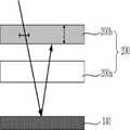
도 1은 본 발명의 유기 발광 표시 장치의 단면도이고, 도 2는 유기 발광 표시 장치로 입사된 외부 광의 진행 방향을 도시한 단면도이다. 그리고, 도 3은 홀을 통해 유기 발광 표시 패널의 광이 외부로 방출되는 것을 도시한 단면도이다.FIG. 1 is a cross-sectional view of an organic light emitting diode display according to the present invention, and FIG. 2 is a cross-sectional view illustrating the traveling direction of external light incident on the OLED display. 3 is a cross-sectional view illustrating the light emitted from the organic light emitting display panel through holes.
도 1을 참조하면, 본 발명의 유기 발광 표시 장치는 적색, 녹색, 청색 서브 픽셀을 포함하는 유기 발광 표시 패널과 유기 발광 표시 패널 하부에 부착된 반사 방지부(200)를 포함한다. 반사 방지부(200)는 유기 발광 표시 패널로 입사된 외부 광이 반사되는 것을 방지하기 위한 것으로, 외부 광에 의해 유기 발광 표시 패널의 시인성이 저하되는 것을 방지할 수 있다.Referring to FIG. 1, the organic light emitting diode display of the present invention includes an organic light emitting display panel including red, green, and blue subpixels, and an
특히, 본 발명의 반사 방지부(200)는 각 서브 픽셀에 대응되도록 형성된 홀(H1, H2, H3)을 포함하여 이루어져, 홀(H1, H2, H3)을 통해 유기 발광 표시 패널에서 방출되는 광이 손실 없이 그대로 출사되어 광 투과율을 향상시킨다. 특히, 효율이 낮은 청색(B) 서브 픽셀에 대응되는 홀(H3)의 크기가 가장 크고, 효율이 높은 녹색(G) 서브 픽셀에 대응되는 홀(H2)의 크기가 가장 작아, 서브 픽셀 별로 상이한 효율을 보상할 수 있다.In particular, the
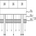
구체적으로, 유기 발광 표시 패널은 제 1 기판(100a)과 제 2 기판(100b), 제 1 기판(100a)과 제 2 기판(100b) 사이에 차례로 형성된 제 1 전극(110), 유기 발광층 및 제 2 전극(140)을 포함하는 적색(R), 녹색(G), 청색(B) 서브 픽셀을 포함한다. 적색, 녹색, 청색 서브 픽셀은 하나의 단위 픽셀을 구성하며, 단위 픽셀은 적색, 녹색, 청색, 백색(White; W) 서브 픽셀, 즉 4개의 서브 픽셀로 구성될 수도 있다.The organic light emitting display panel includes a
적색, 녹색, 청색 서브 픽셀 사이에는 뱅크(120)가 형성되어, 뱅크(120)를 경계부로 하여 적색, 녹색, 청색 서브 픽셀이 분리된다. 그리고, 적색, 녹색, 청색 서브 픽셀은 각각 적색, 녹색, 청색 유기 발광층(130R, 130G, 130B)을 포함한다. 도시하지는 않았으나, 백색(White) 유기 발광층이 전면에 형성되고, 서브 픽셀이 각각 적색, 녹색, 청색 컬러 필터를 포함하여 이루어질 수도 있다. 그리고, 적색, 녹색, 청색, 백색 서브 픽셀이 하나의 단위 픽셀을 구성하는 경우에는, 백색 서브 픽셀에 대응되는 영역에는 컬러 필터가 형성되지 않는다.
제 1, 제 2 기판(100a, 100b)은 투명한 유리 기판인 것이 바람직하며, 제 1 기판(100a) 상에는 다수의 신호 라인, 박막 트랜지스터 및 보호막을 포함하는 셀 구동부가 형성된다. 셀 구동부는 스위치용 박막 트랜지스터와 구동용 박막 트랜지스터 및 스토리지 커패시터를 포함한다. 그리고, 제 2 기판(100b)은 유기 발광 표시 패널을 캐핑(Capping)하기 위한 것이다.The first and
스위치용 박막 트랜지스터는 게이트 라인의 스캔 신호에 응답하여 데이터 라인으로부터의 데이터 신호를 공급하고, 구동용 박막 트랜지스터는 스위치용 박막 트랜지스터로부터의 데이터 신호에 응답하여 연결 전극을 통해 유기 발광 표시 패널에 흐르는 전류량을 제어한다. 그리고, 스토리지 커패시터는 스위치용 박막 트랜지스터가 턴-오프 되더라도 구동용 박막 트랜지스터를 통해 일정한 전류가 흐르게 하는 역할을 한다.The thin film transistor for switching supplies a data signal from the data line in response to a scan signal of the gate line, and the driving thin film transistor has a current amount flowing in the organic light emitting display panel through the connection electrode in response to a data signal from the thin film transistor for switch . The storage capacitor plays a role of allowing a constant current to flow through the thin film transistor for driving even if the thin film transistor for switching is turned off.
구동용 박막 트랜지스터는 제 1 전극(110)과 전기적으로 접속된다. 제 1 전극(110)은 양극(Anode)으로, 틴 옥사이드(Tin Oxide; TO), 인듐 틴 옥사이드(Indium Tin Oxide; ITO), 인듐 징크 옥사이드(Indium Zinc Oxide; IZO), 인듐 틴 징크 옥사이드(Indium Tin Zinc Oxide; ITZO) 등과 같은 투명 도전성 물질로 형성된다. 따라서, 유기 발광층(130)에서 발생된 광이 투명한 제 1 전극(410)을 통과하여 제 1 기판(100a)을 통해 하부로 방출될 수 있다.The driving thin film transistor is electrically connected to the
제 2 전극(140)은 음극(Cathode)으로, 일함수가 낮은 마그네슘(Mg), 은(Ag), 알루미늄(Al), 칼슘(Ca) 등과 같은 불투명 도전성 물질 및 이들의 합금으로 이루어진 군에서 선택된 어느 하나 이상으로 형성될 수 있다. 특히, 제 2 전극(140)은 유기 발광층(130)에서 방출된 광이 반사되어 제 1 기판(100a)을 통해 하부로 방출되도록 반사율이 높은 금속 재질로 형성되는 것이 바람직하다.The
도시하지는 않았으나, 제 1 전극(110)과 유기 발광층(130) 사이에 정공 주입층과 정공 수송층이 더 형성될 수 있으며, 정공 주입층과 정공 수송층은 유기 발광층(130)으로 정공이 잘 주입되도록 하기 위한 것이다. 또한, 유기 발광층(130)과 제 2 전극(140) 사이에 전자 주입층과 전자 수송층이 더 형성될 수 있으며, 전자 주입층과 전자 수송층은 유기 발광층(130)으로 전자가 잘 주입되도록 하기 위한 것이다.Although not shown, a hole injecting layer and a hole transporting layer may be further formed between the
그런데, 유기 발광 표시 장치는 외부 광의 세기에 따라 콘트라스트가 크게 감소하므로, 콘트라스트의 저하를 방지하여 시인성을 향상시키기 위해 반사 방지부(200)를 더 포함하여 이루어진다. 특히, 본 발명의 유기 발광 표시 장치는 상술한 바와 같이, 제 1 기판(100a)을 통해 외부로 광을 방출시키는 하부 발광 방식이므로, 제 1 기판(100a)의 배면에 반사 방지부(200)를 형성한다.However, the organic light emitting display device further includes an
반사 방지부(200)는 차례로 적층된 위상차 필름(200a)과 편광 필름(200b)을 포함한다. 도시하지는 않았으나, 위상차 필름(200a) 상에는 광의 투과를 제한하지 않는 점착성 수지의 점착층이 형성되고, 점착층 상에 편광 필름(200b)이 부착된다.The
도 2와 같이, 유기 발광 표시 장치로 입사되는 외부 광은 편광 필름(200b)의 편광 방향과 동일한 편광 방향을 갖는 광으로 선편광되고, 편광 필름(200b)의 편광 방향과 상이한 편광 방향을 갖는 광은 편광 필름(200b)에 흡수된다. 그리고, 편광 필름(200b)을 통과하며 선편광된 외부 광은 위상차 필름(200a)을 통과한다. 이 때, 위상차 필름(200a)은 편광 필름(200b)의 편광 방향에서 λ/4(±45°)정도 틀어진 광축을 가지므로, 외부 광은 진동 방향이 회전운동을 하도록 원편광된다.2, external light incident on the organic light emitting display device is linearly polarized by light having the same polarization direction as the polarization direction of the
그리고, 원편광된 외부 광은 차례로 제 1 기판(100a), 제 1 전극(110) 및 유기 발광층(130)을 통과한 후, 제 2 전극(140)에서 반사되어 외부 광의 회전방향이 역전된다. 그리고, 다시 차례로 유기 발광층(130), 제 1 전극(110) 및 제 1 기판(100a)을 통과한 후, 위상차 필름(200a)으로 입사되며, 위상차 필름(200a)을 통과한 외부 광은 선편광된다.The circularly polarized external light sequentially passes through the
이 때, 위상차 필름(200a)을 통과하여 다시 선편광된 외부 광의 편광 방향과 위상차 필름(200a)을 통과하지 않은 선편광의 편광 방향이 수직이므로, 선편광된 외부 광은 편광 필름(200b)의 편광 방향과 90°를 이룬다. 따라서, 위상차 필름(200a)을 통과하여 선편광된 외부 광은 편광 필름(200b)을 통과하지 못하므로 외부로 방출되지 못하고 편광 필름(200b)에서 흡수되어 차단된다.At this time, since the polarization direction of the external light that has passed through the
그런데, 상술한 바와 같이, 일반적인 유기 발광 표시 장치는 유기 발광 표시 패널에서 외부로 방출되는 광의 50% 이상을 반사 방지부(200)가 흡수하여 광 효율이 저하된다. 즉, 외부 광의 반사를 방지하여 야외 시인성을 향상시키기 위한 반사 방지부(200)로 인해, 유기 발광 표시 장치의 광 투과율이 저하되는 것이다.However, as described above, in general organic light emitting display devices, more than 50% of the light emitted to the outside from the organic light emitting display panel is absorbed by the
따라서, 본 발명의 유기 발광 표시 장치는 반사 방지부(200)에 제 1 기판(100a)을 노출시키는 홀(H1, H2, H3)을 형성한다. 즉, 각 서브 픽셀에 대응되는 영역에 홀(H1, H2, H3)을 형성하여, 적색, 녹색, 청색 유기 발광층(130R, 130G, 130B)에서 방출되는 광이 홀(H1, H2, H3)을 통해 외부로 바로 방출된다.Therefore, the organic light emitting display of the present invention forms holes H1, H2, and H3 for exposing the
구체적으로, 도 3과 같이, 적색, 녹색, 청색 유기 발광층(130R, 130G, 130B)에서 발생된 광은 투명한 제 1 기판(100a)과 반사 방지부(200)를 통해서 외부로 방출되는데, 반사 방지부(200)에 형성된 홀(H1, H2, H3)을 통해 외부로 방출되는 광은 광 손실 없이 그대로 출사된다. 따라서, 홀(H1, H2, H3)이 형성된 본 발명의 반사 방지부(200)는 일반적인 반사 방지부보다 투과율이 약 42% 이상 증가한다.3, the light generated from the red, green and blue organic
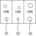
도 4a는 R, G, B 서브 픽셀 마다 하나의 홀이 형성된 것을 도시한 평면도이며, 도 4b는 R, G, B 서브 픽셀 마다 복수 개의 홀이 형성된 것을 도시한 평면도이다.FIG. 4A is a plan view showing one hole formed for each R, G, and B sub-pixels, and FIG. 4B is a plan view illustrating formation of a plurality of holes for R, G, and B sub-pixels.
도 4a와 같이, 각 적색, 녹색, 청색 서브 픽셀에 하나의 홀(H1, H2, H3)이 형성될 수 있다. 특히, 적색, 녹색, 청색 서브 픽셀의 효율이 동일하지 않으므로, 적색, 녹색, 청색 서브 픽셀마다 홀의 크기가 상이한 것이 바람직하다.As shown in FIG. 4A, one hole H1, H2, and H3 may be formed in each of the red, green, and blue subpixels. In particular, since the efficiencies of the red, green, and blue subpixels are not the same, it is preferable that the sizes of the holes are different for the red, green, and blue subpixels.
구체적으로, 청색 서브 픽셀의 효율이 가장 낮고, 녹색 서브 픽셀의 효율이 가장 높으므로, 적색, 녹색, 청색 서브 픽셀에 각각 형성된 홀(H1, H2, H3) 중 청색 서브 픽셀에 형성되는 홀(H3)의 크기가 가장 크며, 녹색 서브 픽셀에 대응되는 홀(H2)의 크기가 가장 작다. 따라서, 적색, 녹색, 청색 서브 픽셀이 균일한 효율을 가질 수 있다.Specifically, since the efficiency of the blue subpixel is the lowest and the efficiency of the green subpixel is the highest, the hole H3 (H3) formed in the blue subpixel among the holes H1, H2 and H3 formed in the red, green, And the size of the hole H2 corresponding to the green sub-pixel is the smallest. Thus, the red, green, and blue subpixels can have a uniform efficiency.
특히, 도 4b와 같이, 홀(H1, H2, H3)은 적색, 녹색, 청색 서브 픽셀에 복수 개 형성될 수 있다. 홀(H1, H2, H3)이 복수 개 형성된 경우에도, 효율이 가장 높은 녹색 서브 픽셀에 형성된 홀(H2)의 총 크기가 효율이 가장 낮은 청색 서브 픽셀에 형성된 홀(H3)의 총 크기보다 작은 것이 바람직하다.In particular, as shown in FIG. 4B, a plurality of holes H1, H2, and H3 may be formed in the red, green, and blue subpixels. Even when a plurality of holes H1, H2 and H3 are formed, the total size of the holes H2 formed in the green subpixels having the highest efficiency is smaller than the total size of the holes H3 formed in the blue subpixels having the lowest efficiency .
즉, 상기와 같은 본 발명의 유기 발광 표시 장치는 반사 방지부(200)에 홀(H1, H2, H3)을 형성하여, 유기 발광 표시 패널에서 방출되는 광의 투과율을 향상시킬 수 있다. 그리고, 광 투과율이 향상됨에 따라, 일반적인 유기 발광 표시 장치보다 적은 구동 전류로 장치를 구동시켜, 발광 효율 및 수명을 향상시키고 소비 전력을 감소시킬 수 있다. 특히, 홀(H1, H2, H3)의 크기가 적색, 녹색, 청색 서브 픽셀마다 상이하여, 적색, 녹색, 청색 서브 픽셀이 균일한 효율을 가질 수 있다.That is, the organic light emitting display of the present invention can improve the transmittance of light emitted from the organic light emitting display panel by forming the holes H1, H2, and H3 in the
이하, 첨부된 도면을 참조하여, 본 발명의 유기 발광 표시 장치의 제조 방법을 구체적으로 설명하면 다음과 같다.Hereinafter, a method of manufacturing an organic light emitting display according to an embodiment of the present invention will be described in detail with reference to the accompanying drawings.
도 5a 내지 도 5d는 본 발명의 유기 발광 표시 장치의 제조 방법을 나타낸 공정 단면도이다.5A to 5D are cross-sectional views illustrating a method of manufacturing an organic light emitting display according to an embodiment of the present invention.
구체적으로, 본 발명의 유기 발광 표시 장치의 제조 방법은 도 5a와 같이, 제 1 기판(100a) 상에 각각 제 1 전극(110), 제 1 전극(110) 상에 차례로 형성된 유기 발광층(130R, 130G, 130B) 및 제 2 전극(140)을 포함하는 적색(R), 녹색(G), 청색(B) 서브 픽셀을 형성한다. 이 때, 적색, 녹색, 청색 서브 픽셀 사이에는 뱅크(120)가 형성되며, 뱅크(120)를 경계부로 하여 적색, 녹색, 청색 서브 픽셀이 분리된다. 그리고, 도 5b와 같이, 제 2 전극(140) 상에 제 2 기판(100b)을 형성한다. 제 2 기판(100b)은 유기 발광 표시 패널을 캐핑하기 위한 것이다.5A, a
이어, 도 5c와 같이, 제 1 기판(100a) 배면에 반사 방지부(200)를 부착한다. 반사 방지부(200)는 차례로 적층된 위상차 필름(200a)과 편광 필름(200b)을 포함한다. 그리고, 도 5d와 같이, 레이저를 이용하여 반사 방지부(200)에 홀(H1, H2, H3)을 형성한다.Next, as shown in FIG. 5C, the
이 때, 위상차 필름(200a)과 편광 필름(200b)의 두께가 얇으므로, 열 데미지(Damage)가 적은 IR(Infrared Ray) 레이저 또는 UV(Ultraviolet Ray) 레이저를 이용하여 홀(H1, H2, H3)을 형성하는 것이 바람직하다. 또한, 레이저는 연속적인(Continuous) 형태가 아닌 펄스(Pulse) 형태로 조사하는 것이 바람직하다.At this time, since the thicknesses of the
반사 방지부(200)에 형성된 홀(H1, H2, H3)은 적색, 녹색, 청색 서브 픽셀에서 방출되는 광을 바로 외부로 방출시키기 위한 것으로, 적색, 녹색, 청색 서브 픽셀마다 홀(H1, H2, H3)의 크기가 상이하다. 이는, 적색, 녹색, 청색 서브 픽셀의 효율이 상이하므로, 홀(H1, H2, H3)의 크기를 다르게 형성하여, 적색, 녹색, 청색 서브 픽셀이 균일한 효율을 갖도록 하기 위함이다.The holes H1, H2, and H3 formed in the
즉, 청색 서브 픽셀의 효율이 가장 낮고, 녹색 서브 픽셀의 효율이 가장 높으므로, 청색 서브 픽셀에 형성되는 홀(H3)의 크기가 가장 크며, 녹색 서브 픽셀에 대응되는 홀(H2)의 크기가 가장 작다.That is, since the efficiency of the blue sub-pixel is the lowest and the efficiency of the green sub-pixel is the highest, the size of the hole H3 formed in the blue sub-pixel is the largest and the size of the hole H2 corresponding to the green sub- It is the smallest.
특히, 도면에서는 제 1 기판(100a) 배면에 반사 방지부(200)를 부착한 후, 레이저를 이용하여 홀(H1, H2, H3)을 형성하는 것을 도시하였으나, 먼저, 반사 방지부(200)에 홀(H1, H2, H3)을 형성하고, 홀(H1, H2, H3)이 형성된 반사 방지부(200)를 제 1 기판(100a) 배면에 부착하여도 무방하다. 그런데, 이 경우에는 반사 방지부(200)에 형성된 홀(H1, H2, H3)이 각 서브 픽셀에 대응되도록 ±10㎛ 정도의 마진이 필요하며, 반사 방지부(200)과 유기 발광 표시 패널을 얼라인하기 위한 기구가 추가로 필요하다. 따라서, 도면과 같이, 반사 방지부(200)를 부착한 후, 홀(H1, H2, H3)을 형성하는 것이 바람직하다.In particular, in the drawing, the holes H1, H2, and H3 are formed by using a laser after attaching the
즉, 상기와 같은 본 발명의 유기 발광 표시 장치는 유기 발광 표시 패널 상에 홀(H1, H2, H3)이 형성된 반사 방지부(200)를 구비하여, 유기 발광 표시 패널에서 방출되는 광이 홀(H1, H2, H3)을 통해 손실 없이 그대로 출사되므로, 유기 발광 표시 장치의 투과율을 향상시킬 수 있다. 특히, 효율이 가장 낮은 B 서브 픽셀에 대응되는 홀(H3)의 크기가 가장 크며, 효율이 가장 높은 G 서브 픽셀에 대응되는 홀(H2)의 크기가 가장 작아, R, G, B 서브 픽셀이 균일한 효율을 가질 수 있다.That is, the OLED display according to the present invention includes the OLED display panel having the holes H1, H2, and H3 formed thereon, H1, H2, and H3), so that the transmittance of the OLED display device can be improved. In particular, the size of the hole H3 corresponding to the B sub-pixel having the lowest efficiency is the largest, and the size of the hole H2 corresponding to the G sub-pixel having the highest efficiency is the smallest, And can have a uniform efficiency.
그리고, 광 투과율이 향상됨에 따라, 일반적인 유기 발광 표시 장치보다 적은 구동 전류로 유기 발광 표시 장치가 구동되어 발광 효율과 수명을 향상시키고, 소비 전력을 감소시킬 수 있다.As the light transmittance is improved, the organic light emitting display device is driven with a driving current smaller than that of a general organic light emitting display device, thereby improving luminous efficiency and lifetime and reducing power consumption.
한편, 이상에서 설명한 본 발명은 상술한 실시 예 및 첨부된 도면에 한정되는 것이 아니고, 본 발명의 기술적 사상을 벗어나지 않는 범위 내에서 여러 가지 치환, 변형 및 변경이 가능하다는 것이 본 발명이 속하는 기술분야에서 통상의 지식을 가진 자에게 있어 명백할 것이다.While the present invention has been described in connection with what is presently considered to be the most practical and preferred embodiment, it is to be understood that the invention is not limited to the disclosed embodiments, but, on the contrary, is intended to cover various modifications and equivalent arrangements included within the spirit and scope of the appended claims. Will be apparent to those of ordinary skill in the art.
100a: 제 1 기판100b: 제 2 기판
110: 제 1 전극120: 뱅크
130: 유기 발광층130R: 적색 유기 발광층
130G: 녹색 유기 발광층130B: 청색 유기 발광층
140: 제 2 전극200: 반사 방지부
200a: 위상차 필름200b: 편광 필름
H1, H2, H3: 홀100a:
110: first electrode 120: bank
130: organic
130G: green organic
140: second electrode 200: antireflection part
200a:
H1, H2, H3: Hole
Claims (9)
Translated fromKorean상기 제 1 기판 상에 형성되며, 각각 제 1 전극, 상기 제 1 전극 상에 차례로 형성된 유기 발광층 및 제 2 전극을 포함하는 적색, 녹색, 청색 서브 픽셀;
상기 적색, 녹색, 청색 서브 픽셀 상에 형성되는 제 2 기판; 및
상기 제 1 기판 배면에 차례로 형성되는 위상차 필름과 편광 필름을 포함하는 반사 방지부를 포함하며,
상기 반사 방지부는 상기 적색, 녹색, 청색 서브 픽셀에서 방출되는 광을 투과시키는 홀을 포함하며, 상기 적색, 녹색, 청색 서브 픽셀마다 상기 홀의 크기가 상이한 것을 특징으로 하는 유기 발광 표시 장치.A first substrate;
Red, green, and blue subpixels formed on the first substrate, each including a first electrode, an organic light emitting layer sequentially formed on the first electrode, and a second electrode;
A second substrate formed on the red, green, and blue subpixels; And
And an antireflection portion including a retardation film and a polarizing film sequentially formed on a back surface of the first substrate,
Wherein the reflection preventing portion includes a hole for transmitting light emitted from the red, green, and blue subpixels, and the hole size is different for each of the red, green, and blue subpixels.
상기 청색 서브 픽셀에 대응되는 상기 홀의 크기가 가장 크며, 상기 녹색 서브 픽셀에 대응되는 상기 홀의 크기가 가장 작은 것을 특징으로 하는 유기 발광 표시 장치.The method according to claim 1,
Wherein the hole corresponding to the blue subpixel is the largest and the hole corresponding to the green subpixel has the smallest hole size.
상기 홀은 상기 R, G, B 서브 픽셀마다 복수 개 형성된 것을 특징으로 하는 유기 발광 표시 장치.The method according to claim 1,
And a plurality of holes are formed for each of the R, G, and B sub-pixels.
상기 적색, 녹색, 청색 서브 픽셀 상에 형성되는 제 2 기판을 형성하는 단계; 및
상기 제 1 기판 배면에 차례로 형성된 위상차 필름과 편광 필름을 포함하는 반사 방지부를 형성하는 단계를 포함하며,
상기 반사 방지부는 상기 적색, 녹색, 청색 서브 픽셀에서 방출되는 광을 투과시키는 홀을 포함하며, 상기 적색, 녹색, 청색 서브 픽셀마다 상기 홀의 크기가 상이한 것을 특징으로 하는 유기 발광 표시 장치의 제조 방법.Forming red, green, and blue subpixels on the first substrate, the red, green, and blue subpixels including a first electrode, an organic light emitting layer sequentially formed on the first electrode, and a second electrode;
Forming a second substrate on the red, green, and blue subpixels; And
And forming an antireflection portion including a retardation film and a polarizing film sequentially formed on the back surface of the first substrate,
Wherein the reflection preventing portion includes a hole for transmitting light emitted from the red, green, and blue subpixels, and the hole size is different for each of the red, green, and blue subpixels.
레이저를 이용하여 상기 홀을 형성하는 것을 특징으로 하는 유기 발광 표시 장치의 제조 방법.5. The method of claim 4,
Wherein the hole is formed using a laser.
상기 레이저는 IR 레이저 또는 UV 레이저인 것을 특징으로 하는 유기 발광 표시 장치의 제조 방법.6. The method of claim 5,
Wherein the laser is an IR laser or a UV laser.
상기 홀은 상기 반사 방지부를 부착하기 전에 형성하거나, 상기 반사 방지부를 부착한 후 형성하는 것을 특징으로 하는 유기 발광 표시 장치의 제조 방법.5. The method of claim 4,
Wherein the hole is formed before or after attaching the antireflection portion to the organic light emitting display device.
상기 청색 서브 픽셀에 대응되는 상기 홀의 크기가 가장 크며, 상기 녹색 서브 픽셀에 대응되는 상기 홀의 크기가 가장 작은 것을 특징으로 하는 유기 발광 표시 장치의 제조 방법.5. The method of claim 4,
Wherein the hole corresponding to the blue subpixel has the largest size and the hole corresponding to the green subpixel has the smallest hole size.
상기 홀을 상기 R, G, B 서브 픽셀마다 복수 개 형성하는 것을 특징으로 하는 유기 발광 표시 장치의 제조 방법.5. The method of claim 4,
And a plurality of holes are formed for each of the R, G, and B sub-pixels.
Priority Applications (1)
| Application Number | Priority Date | Filing Date | Title |
|---|---|---|---|
| KR1020120036670AKR101830613B1 (en) | 2012-04-09 | 2012-04-09 | Organic light emitting device and method for fabricating the same |
Applications Claiming Priority (1)
| Application Number | Priority Date | Filing Date | Title |
|---|---|---|---|
| KR1020120036670AKR101830613B1 (en) | 2012-04-09 | 2012-04-09 | Organic light emitting device and method for fabricating the same |
Publications (2)
| Publication Number | Publication Date |
|---|---|
| KR20130114374A KR20130114374A (en) | 2013-10-18 |
| KR101830613B1true KR101830613B1 (en) | 2018-02-21 |
Family
ID=49634423
Family Applications (1)
| Application Number | Title | Priority Date | Filing Date |
|---|---|---|---|
| KR1020120036670AActiveKR101830613B1 (en) | 2012-04-09 | 2012-04-09 | Organic light emitting device and method for fabricating the same |
Country Status (1)
| Country | Link |
|---|---|
| KR (1) | KR101830613B1 (en) |
Cited By (1)
| Publication number | Priority date | Publication date | Assignee | Title |
|---|---|---|---|---|
| US11812649B2 (en) | 2020-05-15 | 2023-11-07 | Samsung Display Co., Ltd. | Display device that prevents deterioration due to external light |
Families Citing this family (5)
| Publication number | Priority date | Publication date | Assignee | Title |
|---|---|---|---|---|
| KR102092082B1 (en)* | 2013-11-11 | 2020-03-23 | 엘지디스플레이 주식회사 | Organic Light Emitting Display Device and Method of manufacturing the same |
| CN104659075B (en)* | 2015-03-19 | 2017-08-08 | 京东方科技集团股份有限公司 | OLED display panel and its manufacture method, display device |
| KR102742749B1 (en)* | 2018-12-11 | 2024-12-12 | 엘지디스플레이 주식회사 | Organic light emitting diode display device |
| CN110649178B (en) | 2019-09-26 | 2022-05-20 | 京东方科技集团股份有限公司 | A display panel, its manufacturing method and display device |
| KR102852675B1 (en)* | 2019-12-30 | 2025-08-28 | 엘지디스플레이 주식회사 | Display Device |
- 2012
- 2012-04-09KRKR1020120036670Apatent/KR101830613B1/enactiveActive
Cited By (1)
| Publication number | Priority date | Publication date | Assignee | Title |
|---|---|---|---|---|
| US11812649B2 (en) | 2020-05-15 | 2023-11-07 | Samsung Display Co., Ltd. | Display device that prevents deterioration due to external light |
Also Published As
| Publication number | Publication date |
|---|---|
| KR20130114374A (en) | 2013-10-18 |
Similar Documents
| Publication | Publication Date | Title |
|---|---|---|
| KR102252169B1 (en) | Display unit and electronic apparatus | |
| CN102956673B (en) | Organic light emitting diode display and its manufacture method | |
| US6900458B2 (en) | Transflective display having an OLED backlight | |
| TWI584461B (en) | display screen | |
| US20160087245A1 (en) | Organic light emitting diode device | |
| US20050088084A1 (en) | Organic polarized light emitting diode display with polarizer | |
| US9223065B2 (en) | Optical film and organic light-emitting display device including the same | |
| US20060187384A1 (en) | Display device | |
| KR101830613B1 (en) | Organic light emitting device and method for fabricating the same | |
| KR20150129551A (en) | Display apparatus and manufacturing method of the same | |
| KR20140106868A (en) | Organic light emitting display and manufactucring method of the same | |
| TW201624792A (en) | Display with gray filter | |
| CN108029178B (en) | Organic electroluminescent device, method for manufacturing organic electroluminescent device, lighting device, and display device | |
| KR20170064164A (en) | Organic light emitting diode display device | |
| JP2013038014A (en) | Display device and electronic apparatus | |
| US9721999B2 (en) | Pixel element structure, array structure and display device | |
| US20240206303A1 (en) | Display Substrate and Display Device | |
| EP2157631B1 (en) | Organic light emitting diode display | |
| US20220085326A1 (en) | Display apparatus and method of manufacturing the same | |
| EP2197061B1 (en) | Organic light emitting diode display | |
| KR20150077178A (en) | Organic light emitting device | |
| CN111200079B (en) | Organic light emitting diode display device and display device | |
| KR102603593B1 (en) | Display device having a white light emitting layer | |
| KR20160001311A (en) | Organic light emitting display panel | |
| KR101888438B1 (en) | Organic light emitting device |
Legal Events
| Date | Code | Title | Description |
|---|---|---|---|
| PA0109 | Patent application | Patent event code:PA01091R01D Comment text:Patent Application Patent event date:20120409 | |
| PG1501 | Laying open of application | ||
| A201 | Request for examination | ||
| PA0201 | Request for examination | Patent event code:PA02012R01D Patent event date:20170404 Comment text:Request for Examination of Application Patent event code:PA02011R01I Patent event date:20120409 Comment text:Patent Application | |
| E701 | Decision to grant or registration of patent right | ||
| PE0701 | Decision of registration | Patent event code:PE07011S01D Comment text:Decision to Grant Registration Patent event date:20180118 | |
| GRNT | Written decision to grant | ||
| PR0701 | Registration of establishment | Comment text:Registration of Establishment Patent event date:20180213 Patent event code:PR07011E01D | |
| PR1002 | Payment of registration fee | Payment date:20180214 End annual number:3 Start annual number:1 | |
| PG1601 | Publication of registration | ||
| PR1001 | Payment of annual fee | Payment date:20210118 Start annual number:4 End annual number:4 | |
| PR1001 | Payment of annual fee | Payment date:20220120 Start annual number:5 End annual number:5 | |
| PR1001 | Payment of annual fee | Payment date:20230116 Start annual number:6 End annual number:6 | |
| PR1001 | Payment of annual fee | Payment date:20240115 Start annual number:7 End annual number:7 | |
| PR1001 | Payment of annual fee | Payment date:20250115 Start annual number:8 End annual number:8 |