KR101829067B1 - Display device with touch detection function and electronic unit - Google Patents
Display device with touch detection function and electronic unitDownload PDFInfo
- Publication number
- KR101829067B1 KR101829067B1KR1020110084373AKR20110084373AKR101829067B1KR 101829067 B1KR101829067 B1KR 101829067B1KR 1020110084373 AKR1020110084373 AKR 1020110084373AKR 20110084373 AKR20110084373 AKR 20110084373AKR 101829067 B1KR101829067 B1KR 101829067B1
- Authority
- KR
- South Korea
- Prior art keywords
- touch detection
- electrode
- electrodes
- display device
- effective display
- Prior art date
- Legal status (The legal status is an assumption and is not a legal conclusion. Google has not performed a legal analysis and makes no representation as to the accuracy of the status listed.)
- Active
Links
Images


Classifications
- G—PHYSICS
- G06—COMPUTING OR CALCULATING; COUNTING
- G06F—ELECTRIC DIGITAL DATA PROCESSING
- G06F3/00—Input arrangements for transferring data to be processed into a form capable of being handled by the computer; Output arrangements for transferring data from processing unit to output unit, e.g. interface arrangements
- G06F3/01—Input arrangements or combined input and output arrangements for interaction between user and computer
- G06F3/03—Arrangements for converting the position or the displacement of a member into a coded form
- G06F3/041—Digitisers, e.g. for touch screens or touch pads, characterised by the transducing means
- G06F3/044—Digitisers, e.g. for touch screens or touch pads, characterised by the transducing means by capacitive means
- G06F3/0445—Digitisers, e.g. for touch screens or touch pads, characterised by the transducing means by capacitive means using two or more layers of sensing electrodes, e.g. using two layers of electrodes separated by a dielectric layer
- G—PHYSICS
- G06—COMPUTING OR CALCULATING; COUNTING
- G06F—ELECTRIC DIGITAL DATA PROCESSING
- G06F3/00—Input arrangements for transferring data to be processed into a form capable of being handled by the computer; Output arrangements for transferring data from processing unit to output unit, e.g. interface arrangements
- G06F3/01—Input arrangements or combined input and output arrangements for interaction between user and computer
- G06F3/03—Arrangements for converting the position or the displacement of a member into a coded form
- G06F3/041—Digitisers, e.g. for touch screens or touch pads, characterised by the transducing means
- G06F3/044—Digitisers, e.g. for touch screens or touch pads, characterised by the transducing means by capacitive means
- G—PHYSICS
- G02—OPTICS
- G02F—OPTICAL DEVICES OR ARRANGEMENTS FOR THE CONTROL OF LIGHT BY MODIFICATION OF THE OPTICAL PROPERTIES OF THE MEDIA OF THE ELEMENTS INVOLVED THEREIN; NON-LINEAR OPTICS; FREQUENCY-CHANGING OF LIGHT; OPTICAL LOGIC ELEMENTS; OPTICAL ANALOGUE/DIGITAL CONVERTERS
- G02F1/00—Devices or arrangements for the control of the intensity, colour, phase, polarisation or direction of light arriving from an independent light source, e.g. switching, gating or modulating; Non-linear optics
- G02F1/01—Devices or arrangements for the control of the intensity, colour, phase, polarisation or direction of light arriving from an independent light source, e.g. switching, gating or modulating; Non-linear optics for the control of the intensity, phase, polarisation or colour
- G02F1/13—Devices or arrangements for the control of the intensity, colour, phase, polarisation or direction of light arriving from an independent light source, e.g. switching, gating or modulating; Non-linear optics for the control of the intensity, phase, polarisation or colour based on liquid crystals, e.g. single liquid crystal display cells
- G02F1/133—Constructional arrangements; Operation of liquid crystal cells; Circuit arrangements
- G02F1/1333—Constructional arrangements; Manufacturing methods
- G02F1/13338—Input devices, e.g. touch panels
- G—PHYSICS
- G06—COMPUTING OR CALCULATING; COUNTING
- G06F—ELECTRIC DIGITAL DATA PROCESSING
- G06F3/00—Input arrangements for transferring data to be processed into a form capable of being handled by the computer; Output arrangements for transferring data from processing unit to output unit, e.g. interface arrangements
- G06F3/01—Input arrangements or combined input and output arrangements for interaction between user and computer
- G06F3/03—Arrangements for converting the position or the displacement of a member into a coded form
- G06F3/041—Digitisers, e.g. for touch screens or touch pads, characterised by the transducing means
- G06F3/0412—Digitisers structurally integrated in a display
- G—PHYSICS
- G06—COMPUTING OR CALCULATING; COUNTING
- G06F—ELECTRIC DIGITAL DATA PROCESSING
- G06F3/00—Input arrangements for transferring data to be processed into a form capable of being handled by the computer; Output arrangements for transferring data from processing unit to output unit, e.g. interface arrangements
- G06F3/01—Input arrangements or combined input and output arrangements for interaction between user and computer
- G06F3/03—Arrangements for converting the position or the displacement of a member into a coded form
- G06F3/041—Digitisers, e.g. for touch screens or touch pads, characterised by the transducing means
- G06F3/047—Digitisers, e.g. for touch screens or touch pads, characterised by the transducing means using sets of wires, e.g. crossed wires
- G—PHYSICS
- G09—EDUCATION; CRYPTOGRAPHY; DISPLAY; ADVERTISING; SEALS
- G09G—ARRANGEMENTS OR CIRCUITS FOR CONTROL OF INDICATING DEVICES USING STATIC MEANS TO PRESENT VARIABLE INFORMATION
- G09G3/00—Control arrangements or circuits, of interest only in connection with visual indicators other than cathode-ray tubes
- G09G3/20—Control arrangements or circuits, of interest only in connection with visual indicators other than cathode-ray tubes for presentation of an assembly of a number of characters, e.g. a page, by composing the assembly by combination of individual elements arranged in a matrix no fixed position being assigned to or needed to be assigned to the individual characters or partial characters
- G09G3/34—Control arrangements or circuits, of interest only in connection with visual indicators other than cathode-ray tubes for presentation of an assembly of a number of characters, e.g. a page, by composing the assembly by combination of individual elements arranged in a matrix no fixed position being assigned to or needed to be assigned to the individual characters or partial characters by control of light from an independent source
- G09G3/36—Control arrangements or circuits, of interest only in connection with visual indicators other than cathode-ray tubes for presentation of an assembly of a number of characters, e.g. a page, by composing the assembly by combination of individual elements arranged in a matrix no fixed position being assigned to or needed to be assigned to the individual characters or partial characters by control of light from an independent source using liquid crystals
- G09G3/3611—Control of matrices with row and column drivers
- G—PHYSICS
- G06—COMPUTING OR CALCULATING; COUNTING
- G06F—ELECTRIC DIGITAL DATA PROCESSING
- G06F2203/00—Indexing scheme relating to G06F3/00 - G06F3/048
- G06F2203/041—Indexing scheme relating to G06F3/041 - G06F3/045
- G06F2203/04101—2.5D-digitiser, i.e. digitiser detecting the X/Y position of the input means, finger or stylus, also when it does not touch, but is proximate to the digitiser's interaction surface and also measures the distance of the input means within a short range in the Z direction, possibly with a separate measurement setup
- G—PHYSICS
- G06—COMPUTING OR CALCULATING; COUNTING
- G06F—ELECTRIC DIGITAL DATA PROCESSING
- G06F2203/00—Indexing scheme relating to G06F3/00 - G06F3/048
- G06F2203/041—Indexing scheme relating to G06F3/041 - G06F3/045
- G06F2203/04111—Cross over in capacitive digitiser, i.e. details of structures for connecting electrodes of the sensing pattern where the connections cross each other, e.g. bridge structures comprising an insulating layer, or vias through substrate
- G—PHYSICS
- G09—EDUCATION; CRYPTOGRAPHY; DISPLAY; ADVERTISING; SEALS
- G09G—ARRANGEMENTS OR CIRCUITS FOR CONTROL OF INDICATING DEVICES USING STATIC MEANS TO PRESENT VARIABLE INFORMATION
- G09G2300/00—Aspects of the constitution of display devices
- G09G2300/04—Structural and physical details of display devices
- G09G2300/0421—Structural details of the set of electrodes
- G09G2300/0426—Layout of electrodes and connections
Landscapes
- Engineering & Computer Science (AREA)
- Theoretical Computer Science (AREA)
- General Engineering & Computer Science (AREA)
- Physics & Mathematics (AREA)
- General Physics & Mathematics (AREA)
- Human Computer Interaction (AREA)
- Crystallography & Structural Chemistry (AREA)
- Chemical & Material Sciences (AREA)
- Nonlinear Science (AREA)
- Computer Hardware Design (AREA)
- Optics & Photonics (AREA)
- Mathematical Physics (AREA)
- Position Input By Displaying (AREA)
- Liquid Crystal (AREA)
Abstract
Translated fromKorean
Description
Translated fromKorean본 발명은, 터치 검출 기능을 갖는 표시 장치에 관한 것으로, 특히 외부 근접 물체에 의한 정전용량의 변화에 의거하여 터치를 검출하는 터치 검출 기능이 있는 표시 장치, 및 그와 같은 터치 검출 기능이 있는 표시 장치를 구비한 전자 기기에 관한 것이다.The present invention relates to a display device having a touch detection function, and more particularly to a display device having a touch detection function for detecting a touch based on a change in capacitance due to an external proximity object, and a display device having such a touch detection function And an electronic apparatus having the apparatus.
근래, 이른바 터치 패널이라고 불리는 접촉 검출 장치를 액정 표시 장치 등의 표시 장치상에 장착하고, 또는 터치 패널과 표시 장치를 일체화하고, 그 표시 장치에 각종의 버튼 화상 등을 표시시킴에 의해, 통상의 기계식 버튼의 대용으로서 정보 입력을 가능하게 한 표시 장치가 주목받고 있다. 이와 같은 터치 패널을 갖는 표시 장치는 키보드나 마우스, 키패드와 같은 입력 장치를 필요로 하지 않기 때문에 컴퓨터 외, 휴대 전화와 같은 휴대 정보 단말 등에서도 사용이 확대하는 경향에 있다.2. Description of the Related Art In recent years, a touch detection device called a touch panel is mounted on a display device such as a liquid crystal display device, or a touch panel and a display device are integrated, and various kinds of button images and the like are displayed on the display device, A display device capable of inputting information as a substitute for a mechanical button has been attracting attention. Such a display device having a touch panel does not require an input device such as a keyboard, a mouse, and a keypad, and thus the use of such a display device tends to be expanded also in a portable information terminal such as a cellular phone.
터치 검출 방식에는 몇 가지의 방식이 존재하는데, 그 하나로서 정전용량식이 있다. 예를 들면, 특허 문헌 1에는, 표시 장치에 원래 구비되어 있는 표시용의 공통 전극을, 한 쌍의 터치 센서용 전극 중의 한쪽으로서 겸용하고, 다른쪽의 전극(터치 검출 전극)을 이 공통 전극과 교차하도록 배치한 표시 장치가 제안되어 있다. 또한, 특허 문헌 2에는, X축 방향과 Y축 방향에 따라 형성된 복수의 전극을 구비한 터치 패널이 제안되어 있다. 또한, 특허 문헌 3에는, 하나의 층에, 폭이 장소에 따라 다른 3개의 전극을 구비한 센서 장치가 제안되어 있다. 또한, 특허 문헌 4에는, X축 방향과 Y축 방향에 따라 형성된 복수의 전극을 구비하고, 터치 패널의 조작면에 미스 터치를 막기 위한 요철을 마련함과 함께, 그 요철이 있어도 정전용량이 일정하게 되도록 구성된 터치 패널이 제안되어 있다.There are several types of touch detection methods, one of which is the capacitance type. For example,
[특허 문헌][Patent Literature]
특허 문헌 1 : 일본 특개2009-244958호 공보Patent Document 1: JP-A-2009-244958
특허 문헌 2 : 일본 특개2008-217784호 공보Patent Document 2: Japanese Patent Application Laid-Open No. 2008-217784
특허 문헌 3 : 미국 특허 제7382139호 명세서Patent Document 3: U.S. Patent No. 7382139
특허 문헌 4 : 일본 특개2008-86236호 공보Patent Document 4: JP-A-2008-86236
일반적으로 터치 검출 장치에서는, 그 터치 검출면 내에서 검출 감도가 균일할 것이 요망되고 있다. 그러나 정전용량식의 터치 검출 장치에서는, 예를 들면, 터치 검출면의 끝의 영역에서의 검출 감도가, 검출면의 중앙부에서의 검출 감도보다 낮아지는 등 검출 감도의 균일성이 저하될 우려가 있다. 그러나 특허 문헌 1에 기재된 표시 장치, 특허 문헌 2에 기재된 터치 패널, 특허 문헌 3에 기재된 센서 장치에는, 검출 감도의 균일성에 관한 기재는 없다. 또한, 특허 문헌 4에 기재된 터치 패널에서는, 터치 검출면의 끝의 영역에서의 검출 감도에 관해서는 일체 언급되어 있지 않다.Generally, in the touch detection apparatus, it is desired that the detection sensitivity be uniform within the touch detection plane. However, in the capacitance type touch detection apparatus, for example, there is a fear that the detection sensitivity in the region at the end of the touch detection surface becomes lower than the detection sensitivity in the central portion of the detection surface, thereby lowering the uniformity of the detection sensitivity . However, in the display device described in
본 발명은 이러한 문제점을 감안하여 이루어진 것으로, 그 목적은, 터치에 대한 검출 감도의 균일성을 높일 수 있는 터치 검출 기능이 있는 표시 장치 및 전자 기기를 제공하는 것에 있다.SUMMARY OF THE INVENTION The present invention has been made in view of such problems, and an object of the present invention is to provide a display device and an electronic apparatus having a touch detection function capable of increasing the uniformity of detection sensitivity to a touch.
본 발명의 터치 검출 기능이 있는 표시 장치는, 표시 기능층과, 복수의 터치 검출 전극과, 복수의 구동 전극을 구비하고 있다. 복수의 터치 검출 전극은, 제 1의 방향으로 연재되도록 병설되어 있다. 복수의 구동 전극은, 제 1의 방향과 교차하는 제 2의 방향으로 연재되도록 병설되고, 터치 검출 전극의 교차 부분과 구동 전극에 정전용량을 형성하는 것이다. 상기 복수의 구동 전극은, 표시 기능층의 유효 표시 영역에 배치된 터치 검출 전극 중의 가장 외측에 위치하는 터치 검출 전극의 중심으로부터, 터치 검출 전극의 배열 피치의 반분의 거리만큼 떨어진 제 1의 위치 또는 그 외측의 제 2의 위치까지 연신(延伸)하고, 유효 표시 영역의 외연(outer edge)은, 제 1의 위치 또는 그 내측에 위치하도록 되어 있다.A display device having a touch detection function according to the present invention includes a display function layer, a plurality of touch detection electrodes, and a plurality of drive electrodes. The plurality of touch detection electrodes are juxtaposed so as to extend in the first direction. The plurality of driving electrodes are juxtaposed so as to extend in a second direction intersecting with the first direction and form a capacitance at the intersection of the touch detecting electrode and the driving electrode. The plurality of driving electrodes are arranged at a first position spaced apart from the center of the touch detection electrode located at the outermost one of the touch detection electrodes disposed in the effective display region of the display function layer by a distance of half the arrangement pitch of the touch detection electrodes, And the outer edge of the effective display area is positioned at the first position or the inside thereof.
본 발명의 전자 기기는, 상기 터치 검출 기능이 있는 표시 장치를 구비한 것이고, 예를 들면, 텔레비전 장치, 디지털 카메라, 퍼스널 컴퓨터, 비디오 카메라 또는 휴대 전화 등의 휴대 단말 장치 등이 해당한다.The electronic apparatus of the present invention is equipped with the display device having the touch detection function and corresponds to, for example, a portable terminal device such as a television device, a digital camera, a personal computer, a video camera, or a cellular phone.
본 발명의 터치 검출 기능이 있는 표시 장치 및 전자 기기에서는, 표시 기능층에서 표시가 행하여지고, 구동 전극 및 터치 검출 전극 사이의 정전용량의 변화에 의거하여 외부 근접 물체에 대한 터치 검출이 행하여진다. 이 구동 전극은, 유효 표시 영역 내의 가장 외측의 터치 검출 전극의 중심으로부터 그 배열 피치의 반분의 거리만큼 떨어진 제 1의 위치 또는 그 외측의 제 2의 위치까지 연신되도록 형성되어 있고, 이 가장 외측의 터치 검출 전극의 전기력선은, 내측의 터치 검출 전극의 전기력선과 거의 똑같이 형성된다. 또한, 유효 표시 영역의 외연은, 제 1의 위치 또는 그 내측에 위치하도록 되어 있다.In the display device and the electronic device having the touch detection function of the present invention, display is performed in the display function layer, and touch detection is performed on an external proximity object based on a change in capacitance between the drive electrode and the touch detection electrode. The driving electrode is formed so as to extend from a center of the outermost touch detection electrode in the effective display area to a first position away from the center of the outermost touch detection electrode by a half distance of the arrangement pitch or to a second position outside the first position, The line of electric force of the touch detection electrode is formed almost the same as the line of electric force of the inner touch detection electrode. The outline of the effective display area is located at the first position or the inside thereof.
본 발명의 터치 검출 기능이 있는 표시 장치에서는, 예를 들면, 복수의 구동 전극은, 제 1의 방향에서의 유효 표시 영역의 외측에 병설된 하나 이상의 구동 전극도 포함하고 있어도 좋다. 또한, 예를 들면, 복수의 터치 검출 전극은, 제 2의 방향에서의 유효 표시 영역의 외측에 병설된 하나 이상의 구동 전극도 포함하고 있어도 좋고, 적어도 가장 외측의 구동 전극의 외측에 위치한 제 3의 위치까지 연신되어 있어도 좋다.In the display device having the touch detection function of the present invention, for example, the plurality of driving electrodes may include at least one driving electrode provided outside the effective display region in the first direction. Further, for example, the plurality of touch detection electrodes may include at least one driving electrode provided outside the effective display region in the second direction, or may include at least a third Or may be stretched to the position.
예를 들면, 복수의 터치 검출 전극은, 서로 같은 전극 폭으로 형성됨과 함께, 유효 표시 영역 내에서, 외측에 배치된 터치 검출 전극의 배열 피치는, 내측에 배치된 터치 검출 전극의 배열 피치와 같게 또는 넓게 되어 있어도 좋다.For example, the plurality of touch detection electrodes are formed to have the same electrode width, and the arrangement pitch of the touch detection electrodes arranged on the outside in the effective display area is set to be equal to the arrangement pitch of the touch detection electrodes disposed on the inside Or may be wide.
또한, 복수의 터치 검출 전극은, 예를 들면, 서로 같은 배열 피치로 배치되고, 유효 표시 영역 내에서, 외측에 배치된 터치 검출 전극의 전극 폭은, 내측에 배치된 터치 검출 전극의 전극 폭과 같게 또는 좁게 되어 있어도 좋다.Further, the plurality of touch detection electrodes are arranged at the same arrangement pitch, for example, and the electrode width of the touch detection electrode disposed on the outer side in the effective display area is larger than the electrode width of the touch detection electrode disposed on the inner side May be the same or narrow.
또한, 예를 들면, 복수의 터치 검출 전극의 위에, 적어도 유효 표시 영역을 덮도록 형성된 표면층을 또한 구비하고, 제 2의 방향에서의 외측의 표면층의 두께는, 내측의 표면층의 두께와 같게 또는 얇게 되어 있어도 좋다.For example, a surface layer formed so as to cover at least the effective display region is provided on the plurality of touch detection electrodes, and the thickness of the outer surface layer in the second direction is equal to or thinner than the thickness of the inner surface layer .
또한, 예를 들면, 표시 기능층은, 액정 표시층과, 화소 전극과, 공통 전극을 갖는 것이라도 좋다. 이 경우, 예를 들면, 공통 전극은, 구동 전극과 공용하도록 하여도 좋다. 예를 들면, 공통 전극은, 액정 표시층에서 화소 전극의 반대측에 배치되고, 또는, 액정 표시층과 화소 전극의 사이에 배치되도록 하여도 좋고, 화소 전극에서 액정 표시층의 반대측에 배치되도록 하여도 좋다.For example, the display functional layer may have a liquid crystal display layer, a pixel electrode, and a common electrode. In this case, for example, the common electrode may be shared with the drive electrode. For example, the common electrode may be disposed on the opposite side of the liquid crystal display layer from the pixel electrode, or between the liquid crystal display layer and the pixel electrode, or may be disposed on the opposite side of the liquid crystal display layer from the pixel electrode good.
본 발명의 터치 검출 기능이 있는 표시 장치 및 전자 기기에 의하면, 구동 전극을, 제 1의 위치 또는 그 외측의 제 2의 위치까지 연신함과 함께, 유효 표시 영역의 외연이 제 1의 위치 또는 그 내측에 위치하도록 하였기 때문에, 가장 외측의 터치 검출 전극에 대응하는 영역에서의 검출 감도를, 내측의 터치 검출 전극에 대응하는 영역에서의 검출 감도와 동등하게 할 수 있고, 유효 표시 영역 내에서의 검출 감도의 균일성을 높일 수 있다.According to the display device and the electronic apparatus having the touch detection function of the present invention, the drive electrode is extended to the first position or the second position outside thereof, and the outline of the effective display area is extended to the first position, The detection sensitivity in the region corresponding to the outermost touch detection electrode can be made equal to the detection sensitivity in the region corresponding to the inner touch detection electrode and the detection in the effective display region The uniformity of the sensitivity can be increased.
도 1은 본 발명의 터치 검출 기능이 있는 표시 장치에서의 터치 검출 방식의 기본 원리를 설명하기 위한 도면으로, 손가락이 접촉 또는 근접하지 않은 상태를 도시하는 도면.
도 2는 본 발명의 터치 검출 기능이 있는 표시 장치에서의 터치 검출 방식의 기본 원리를 설명하기 위한 도면으로, 손가락이 접촉 또는 근접한 상태를 도시하는 도면.
도 3은 본 발명의 터치 검출 기능이 있는 표시 장치에서의 터치 검출 방식의 기본 원리를 설명하기 위한 도면으로, 구동 신호 및 터치 검출 신호의 파형의 한 예를 도시하는 도면.
도 4는 본 발명의 제 1의 실시의 형태에 관한 터치 검출 기능이 있는 표시 장치의 한 구성례를 도시하는 평면도 및 단면도.
도 5는 도 4에 도시한 터치 검출 기능이 있는 표시 장치의 개략 단면 구조를 도시하는 단면도.
도 6은 도 4에 도시한 터치 검출 기능이 있는 표시 장치의 화소 배열을 도시하는 회로도.
도 7은 도 5에 도시한 터치 검출 기능이 있는 표시 장치의 공통 전극 및 터치 검출 전극의 한 구성례를 도시하는 사시도.
도 8은 공통 전극 및 터치 검출 전극 사이의 프린지 기인의 전기력선을 도시하는 모식도.
도 9는 제 1의 실시의 형태의 변형례에 관한 터치 검출 기능이 있는 표시 장치의 한 구성례를 도시하는 평면도 및 단면도.
도 10은 제 2의 실시의 형태에 관한 터치 검출 기능이 있는 표시 장치의 한 구성례를 도시하는 평면도 및 단면도.
도 11은 전극 피치를 바꾼 때의 프린지에 의한 전기력선의 변화를 도시하는 모식도.
도 12는 전극 피치와 검출 감도와의 관계를 도시하는 특성도.
도 13은 제 3의 실시의 형태에 관한 터치 검출 기능이 있는 표시 장치의 한 구성례를 도시하는 평면도 및 단면도.
도 14는 전극 폭을 바꾼 때의 프린지에 의한 전기력선의 변화를 도시하는 모식도.
도 15는 전극 폭과 검출 감도와의 관계를 도시하는 특성도.
도 16은 제 4의 실시의 형태에 관한 터치 검출 기능이 있는 표시 장치의 한 구성례를 도시하는 평면도 및 단면도.
도 17은 표면 유리판의 두께를 바꾼 때의 프린지에 의한 전기력선의 변화를 도시하는 모식도.
도 18은 제 5의 실시의 형태에 관한 터치 검출 장치의 한 구성례를 도시하는 평면도 및 단면도.
도 19는 제 6의 실시의 형태에 관한 터치 검출 장치의 한 구성례를 도시하는 평면도 및 단면도.
도 20은 제 7의 실시의 형태에 관한 터치 검출 장치의 한 구성례를 도시하는 평면도 및 단면도이다.
도 21은 실시의 형태를 적용한 터치 검출 기능이 있는 표시 장치 등중, 적용례 1의 외관 구성을 도시하는 사시도.
도 22는 적용례 2의 외관 구성을 도시하는 사시도.
도 23은 적용례 3의 외관 구성을 도시하는 사시도.
도 24는 적용례 4의 외관 구성을 도시하는 사시도.
도 25는 적용례 5의 외관 구성을 도시하는 정면도, 측면도, 상면도 및 하면도.
도 26은 각 실시의 형태 등의 변형례에 관한 터치 검출 기능이 있는 표시 장치의 개략 단면 구조를 도시하는 단면도.BRIEF DESCRIPTION OF THE DRAWINGS Fig. 1 is a view for explaining a basic principle of a touch detection method in a display device having a touch detection function according to the present invention, and showing a state in which a finger is in contact with or not in proximity to the touch detection method. Fig.
2 is a view for explaining a basic principle of a touch detection method in a display device having a touch detection function according to the present invention, and showing a state in which a finger is in contact with or close to a finger.
3 is a diagram for explaining the basic principle of a touch detection method in a display device having a touch detection function of the present invention, and showing an example of a waveform of a drive signal and a touch detection signal;
4 is a plan view and a cross-sectional view showing one configuration example of a display device having a touch detection function according to the first embodiment of the present invention.
5 is a sectional view showing a schematic sectional structure of a display device having a touch detection function shown in Fig.
Fig. 6 is a circuit diagram showing a pixel arrangement of a display device having a touch detection function shown in Fig. 4; Fig.
Fig. 7 is a perspective view showing one configuration example of a common electrode and a touch detection electrode of a display device having a touch detection function shown in Fig. 5; Fig.
8 is a schematic diagram showing an electric line of force as a fringer between the common electrode and the touch detecting electrode.
9 is a plan view and a cross-sectional view showing one configuration example of a display device having a touch detection function according to a modification of the first embodiment;
10 is a plan view and a cross-sectional view showing one configuration example of a display device having a touch detection function according to the second embodiment.
11 is a schematic diagram showing a change of an electric force line by fringe when the electrode pitch is changed.
12 is a characteristic diagram showing the relationship between the electrode pitch and detection sensitivity.
13 is a plan view and a cross-sectional view showing one configuration example of a display device having a touch detection function according to the third embodiment;
14 is a schematic diagram showing a change of an electric force line due to fringe when the electrode width is changed.
Fig. 15 is a characteristic diagram showing the relationship between the electrode width and detection sensitivity. Fig.
Fig. 16 is a plan view and a cross-sectional view showing one configuration example of a display device having a touch detection function according to the fourth embodiment; Fig.
17 is a schematic diagram showing a change in electric force line due to fringe when the thickness of the surface glass plate is changed.
18 is a plan view and a cross-sectional view showing one configuration example of the touch detection device according to the fifth embodiment;
19 is a plan view and a cross-sectional view showing one configuration example of the touch detection device according to the sixth embodiment;
20 is a plan view and a cross-sectional view showing one configuration example of the touch detection device according to the seventh embodiment.
Fig. 21 is a perspective view showing the appearance of the application example 1 among display devices having a touch detection function and the like to which the embodiment is applied; Fig.
22 is a perspective view showing an external configuration of Application Example 2;
23 is a perspective view showing an external configuration of Application Example 3;
24 is a perspective view showing the external configuration of Application Example 4;
25 is a front view, a side view, a top view, and a bottom view showing an external configuration of Application Example 5;
26 is a cross-sectional view showing a schematic sectional structure of a display device having a touch detection function according to a modification of each embodiment or the like.
이하, 본 발명의 실시의 형태에 관해 도면을 참조하여 상세히 설명한다. 또한, 설명은 이하의 순서로 행한다.DESCRIPTION OF THE PREFERRED EMBODIMENTS Hereinafter, embodiments of the present invention will be described in detail with reference to the drawings. The description will be made in the following order.
1. 정전용량식 터치 검출의 기본 원리1. Basic principle of capacitive touch detection
2. 제 1의 실시의 형태(터치 검출 기능이 있는 표시 장치)2. First Embodiment (Display Device Having Touch Detection Function)
3. 제 2의 실시의 형태(터치 검출 기능이 있는 표시 장치)3. Second Embodiment (display device having a touch detection function)
4. 제 3의 실시의 형태(터치 검출 기능이 있는 표시 장치)4. Third Embodiment (display device having a touch detection function)
5. 제 4의 실시의 형태(터치 검출 기능이 있는 표시 장치)5. Fourth embodiment (display device having a touch detection function)
6. 제 5의 실시의 형태(터치 검출 장치)6. Fifth Embodiment (Touch Detection Apparatus)
7. 제 6의 실시의 형태(터치 검출 장치)7. Sixth Embodiment (Touch Detection Apparatus)
8. 제 7의 실시의 형태(터치 검출 장치)8. Seventh Embodiment (Touch Detection Apparatus)
9. 적용례9. Examples
<1. 정전용량식 터치 검출의 기본 원리><1. Basic principle of capacitive touch detection>
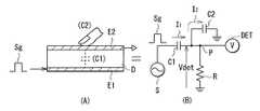
우선, 도 1 내지 도 3을 참조하여, 본 발명의 터치 검출 기능이 있는 표시 장치에서의 터치 검출의 기본 원리에 관해 설명한다. 이 터치 검출 방식은, 정전용량식의 터치 센서로서 구현화된 것이고, 예를 들면 도 1의 (A)에 도시한 바와 같이, 유전체(D)를 끼우고 서로 대향 배치된 한 쌍의 전극(구동 전극(E1) 및 터치 검출 전극(E2))을 이용하여, 용량 소자를 구성한다. 이 구조는, 도 1의 (B)에 도시한 등가 회로로서 표시된다. 구동 전극(E1), 터치 검출 전극(E2) 및 유전체(D)에 의해, 용량 소자(C1)가 구성된다. 용량 소자(C1)는, 그 일단이 교류 신호원(구동 신호원)(S)에 접속되고, 타단(P)은 저항기(R)를 통하여 접지됨과 함께, 전압 검출기(터치 검출 회로)(DET)에 접속된다. 교류 신호원(S)으로부터 구동 전극(E1)(용량 소자(C1)의 일단)에 소정의 주파수(예를 들면 수kHz 내지 수십kHz 정도)의 교류 구형파(Sg)(도 3의 (B))를 인가하면, 터치 검출 전극(E2)(용량 소자(C1)의 타단(P))에, 도 3의 (A)에 도시한 바와 같은 출력 파형(터치 검출 신호(Vdet))이 나타난다. 또한, 이 교류 구형파(Sg)는, 후술하는 구동 신호(Vcom)에 상당하는 것이다.First, the basic principle of touch detection in a display device having a touch detection function of the present invention will be described with reference to Figs. 1 to 3. Fig. This touch detection system is implemented as a capacitive touch sensor. For example, as shown in Fig. 1A, a pair of electrodes (electrodes) sandwiching a dielectric (D) and arranged opposite to each other (E1) and the touch detecting electrode (E2)). This structure is shown as an equivalent circuit shown in Fig. 1 (B). The driving electrode E1, the touch detecting electrode E2 and the dielectric D constitute a capacitive element C1. The capacitive element C1 has one end connected to the AC signal source (drive signal source) S and the other end P grounded through the resistor R and connected to a voltage detector (touch detection circuit) Respectively. An AC square wave Sg (FIG. 3 (B)) having a predetermined frequency (for example, several kHz to several tens kHz) is applied from the AC signal source S to the driving electrode E1 (one end of the capacitive element C1) An output waveform (touch detection signal Vdet) as shown in Fig. 3 (A) appears at the touch detecting electrode E2 (the other end P of the capacitance element C1). The alternating-current square wave Sg corresponds to the drive signal Vcom described later.
예를 들면, 손가락이 표시 장치에 접촉(또는 근접)하지 않는 상태에서는, 도 1에 도시한 바와 같이, 용량 소자(C1)에 대한 충ㆍ방전에 수반하여, 용량 소자(C1)의 용량치에 응한 전류(I0)가 흐른다. 이 때의 용량 소자(C1)의 타단(P)의 전위 파형은, 도 3의 (A)의 파형(V0)과 같이 되고, 이것이 전압 검출기(DET)에 의해 검출된다.For example, as shown in Fig. 1, when the finger is not in contact with (or in proximity to) the display device, the capacitance value of the capacitance element C1 A corresponding current I0 flows. The potential waveform of the other end P of the capacitive element C1 at this time becomes like the waveform V0 of Fig. 3A and is detected by the voltage detector DET.
한편, 손가락이 표시 장치에 접촉(또는 근접)한 상태에서는, 도 2에 도시한 바와 같이, 손가락에 의해 형성되는 용량 소자(C2)가 용량 소자(C1)에 직렬로 추가된 형태가 된다. 이 상태에서는, 용량 소자(C1, C2)에 대한 충ㆍ방전에 수반하여, 각각 전류(I1, I2)가 흐른다. 이 때의 용량 소자(C1)의 타단(P)의 전위 파형은, 예를 들면 도 3의 (A)의 파형(V1)과 같이 되고, 이것이 전압 검출기(DET)에 의해 검출된다. 이 때, 점(P)의 전위는, 용량 소자(C1, C2)를 흐르는 전류(I1, I2)의 값에 의해 정해지는 분압 전위가 된다. 이 때문에, 파형(V1)은, 비접촉 상태에서의 파형(V0)보다도 작은 값이 된다. 전압 검출기(DET)는, 검출한 전압을 소정의 임계치 전압(Vth)과 비교하고, 이 임계치 전압 이상이면 비접촉 상태라고 판단하는 한편, 임계치 전압 미만이면 접촉 상태라고 판단한다. 이와 같이 하여, 터치 검출이 가능해진다. 또한, 이 예에서는, 손가락의 접촉을 예로 설명하였지만, 이것으로 한정되는 것이 아니고, 예를 들면 스타일러스 등이라도 좋다.On the other hand, when the finger is in contact with (or in proximity to) the display device, as shown in Fig. 2, the capacitive element C2 formed by the finger is added in series to the capacitive element C1. In this state, the currents I1 and I2 flow through the capacitive elements C1 and C2 in response to charging / discharging. The potential waveform of the other end P of the capacitive element C1 at this time becomes, for example, the waveform V1 of FIG. 3A and is detected by the voltage detector DET. At this time, the potential of the point P becomes the divided potential determined by the values of the currents I1 and I2 flowing through the capacitive elements C1 and C2. Therefore, the waveform V1 is smaller than the waveform V0 in the non-contact state. The voltage detector DET compares the detected voltage with a predetermined threshold voltage Vth. If the detected voltage is equal to or higher than the threshold voltage, the voltage detector DET determines that it is in the non-contact state. In this way, touch detection becomes possible. In this example, the finger contact has been described as an example, but the present invention is not limited to this. For example, a stylus may be used.
<2. 제 1의 실시의 형태><2. First Embodiment>
[구성례][Configuration Example]
(전체 구성례)(Total configuration example)
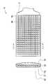
도 4는, 본 발명의 실시의 형태에 관한 터치 검출 기능이 있는 표시 장치의 한 구성례를 도시하는 것이고, 도 5는 도 4의 주요부 단면 구조의 예를 도시하는 것이다. 이 터치 검출 기능이 있는 표시 장치는, 표시 소자로서 액정 표시 소자를 이용하고 있고, 그 액정 표시 소자에 의해 구성된 액정 표시부와 정전용량식의 터치 검출부를 일체화한, 이른바 인 셀(in-cell) 타입의 장치이다.Fig. 4 shows an example of a configuration of a display device having a touch detection function according to an embodiment of the present invention, and Fig. 5 shows an example of a cross-sectional structure of a main part of Fig. This display device having a touch detection function uses a liquid crystal display element as a display element and uses a so-called in-cell type liquid crystal display element in which a liquid crystal display portion constituted by the liquid crystal display element is integrated with a capacitive touch detection portion .
터치 검출 기능이 있는 표시 장치(1)는, 화소 기판(2)과, 이 화소 기판(2)에 대향하여 배치된 대향 기판(3)과, 화소 기판(2)과 대향 기판(3)의 사이에 삽입된 액정층(6)을 구비하고 있다.A
화소 기판(2)은, 도 5에 도시한 바와 같이, 회로 기판으로서의 TFT 기판(21)과, 공통 전극(COML)과, 화소 전극(22)을 갖고 있다. TFT 기판(21)은, 각종 전극이나 배선, 박막 트랜지스터(TFTs) 등이 형성되는 회로 기판으로서 기능 한다. TFT 기판(21)은 예를 들면 유리에 의해 구성되는 것이다. TFT 기판(21)의 위에는, 공통 전극(COML)이 형성된다. 공통 전극(COML)은, 복수의 화소(Pix)(후술)에 공통의 전압을 공급하기 위한 전극이고, 투광성을 갖는 것이다. 또한, 공통 전극(COML)은, 터치 센서에서, 교류 구형파(Sg)를 인가하는 전극으로서도 사용된다. 즉, 공통 전극(COML)은, 상술한 정전용량식 터치 검출의 기본 원리에서의 구동 전극(E1)에 대응하는 것이다. 공통 전극(COML)은, 도 4에 도시한 바와 같이, 터치 검출 기능이 있는 표시 장치(1)가 표시를 행하는 영역인 유효 표시 영역(S) 내에 걸쳐서, 일방향으로 연재되도록 병설되어 있다. 그리고 공통 전극(COML)의 각각은, 이 유효 표시 영역(S)의 외측으로 연신되도록 형성되어 있다. 공통 전극(COML)의 위에는 절연막(23)이 형성되고, 그 위에 화소 전극(22)이 형성된다. 화소 전극(22)은, 표시를 행하기 위한 화소 신호를 공급하기 위한 전극이고, 투광성을 갖는 것이다. 각각의 공통 전극(COML) 및 화소 전극(22)은, 예를 들면 ITO(Indium Tin Oxide)에 의해 구성된다.The
대향 기판(3)은, 도 5에 도시한 바와 같이, 유리 기판(31)과, 컬러 필터(32)와, 터치 검출 전극(TDL)을 갖고 있다. 컬러 필터(32)는, 유리 기판(31)의 한쪽의 면에 형성되어 있다. 이 컬러 필터(32)는, 예를 들면 적(R), 녹(G), 청(B)의 3색의 컬러 필터 층을 주기적으로 배열하여 구성한 것으로, 각 표시 화소에 R, G, B의 3색이 1조로서 대응되어 있다. 또한, 유리 기판(31)의 다른 쪽의 면에는, 터치 검출 전극(TDL)이, 유효 표시 영역(S) 내에 걸쳐서, 공통 전극(COML)과 교차하는 방향으로 연재되도록 병설되어 있다. 터치 검출 전극(TDL)은, 터치 센서에서, 터치 검출 신호(Vdet)를 출력하는 전극이다. 즉, 터치 검출 전극(TDL)은, 상술한 정전용량식 터치 검출의 기본 원리에서의 터치 검출 전극(E2)에 대응하는 것이다. 터치 검출 전극(TDL)은, 예를 들면 ITO에 의해 구성되고, 투광성을 갖는 전극이다. 터치 검출 전극(TDL)은, 터치 검출 신호(Vdet)를 외부에 출력하기 위한 플렉시블 프린트 기판(FPC)(5)에 접속되어 있다. 이 터치 검출 전극(TDL)의 위에는, 편광판(35)이 배설되어 있고, 그 위에는, 표면 유리판(도시 생략)이 배치되어 있다.The
액정층(6)은, 표시 기능층으로서 기능하는 것이고, 전계(electric field)의 상태에 응하여 그곳을 통과하는 광을 변조하는 것이다. 이 전계는, 공통 전극(COML)의 전압과 화소 전극(22)의 전압의 전위차에 의해 형성된다. 액정층(6)에는, FFS(프린지 필드 스위칭)나 IPS(인 플레인 스위칭) 등의 횡전계 모드의 액정이 사용된다. 액정층(6)은, 화소 기판(2)과 대향 기판(3)의 사이에, 실(seal)(4)에 의해 밀봉되어 있다.The
또한, 액정층(6)과 화소 기판(2)의 사이, 및 액정층(6)과 대향 기판(3)의 사이에는, 각각 배향막이 배설되고, 또한, 화소 기판(2)의 하면측에는 입사측 편광판이 배치되지만, 여기서는 도시를 생략하고 있다.An alignment film is provided between the
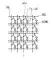
도 6은, 터치 검출 기능이 있는 표시 장치(1)에서의 화소 구조의 구성례를 도시하는 것이다. 터치 검출 기능이 있는 표시 장치(1)는, 매트릭스형상으로 배열한 복수의 화소(Pix)를 갖고 있다. 각 화소(Pix)는, TFT 소자(Tr) 및 액정 소자(LC)를 갖고 있다. TFT 소자(Tr)는, 박막 트랜지스터에 의해 구성되는 것이고, 이 예에서는, n채널의 MOS(Metal Oxide Semiconductor)형의 TFT로 구성되어 있다. TFT 소자(Tr)의 소스는 화소 신호선(SGL)에 접속되고, 게이트는 주사 신호선(GCL)에 접속되고, 드레인은 액정 소자(LC)의 일단에 접속되어 있다. 액정 소자(LC)는, 일단이 TFT 소자(Tr)의 드레인에 접속되고, 타단이 공통 전극(COML)에 접속되어 있다.Fig. 6 shows a configuration example of the pixel structure in the
각 화소(Pix)는, 주사 신호선(GCL)에 의해, 터치 검출 기능이 있는 표시 장치(1)의 같은 행에 속하는 다른 화소(Pix)와 서로 접속되어 있다. 또한, 각 화소(Pix)는, 화소 신호선(SGL)에 의해, 터치 검출 기능이 있는 표시 장치(1)의 같은 열에 속하는 다른 화소(Pix)와 서로 접속되어 있다. 또한, 각 화소(Pix)는, 공통 전극(COML)에 의해, 터치 검출 기능이 있는 표시 장치(1)의 같은 행에 속하는 다른 화소(Pix)와 서로 접속되어 있다.Each pixel Pix is connected to another pixel Pix belonging to the same row of the
도 7은, 터치 검출 기능이 있는 표시 장치(1)에서의 터치 센서의 한 구성례를 도시하는 사시도이다. 이 터치 센서는, 화소 기판(2)에 마련된 공통 전극(COML) 및 대향 기판(3)에 마련된 터치 검출 전극(TDL)에 의해 구성되어 있다. 각 공통 전극(COML)은, 도면의 좌우 방향으로 연재되는 복수의 스트라이프형상의 전극 패턴에 의해 구성되어 있다. 터치 검출 동작을 행할 때는, 각 전극 패턴에는, 구동 신호(Vcom)(상술한 정전용량식 터치 검출의 기본 원리에서의 교류 구형파(Sg)에 대응)가 순차적으로 공급되고, 시분할적으로 순차적인 주사 구동이 행하여지도록 되어 있다. 각 터치 검출 전극(TDL)은, 각 공통 전극(COML)의 전극 패턴의 연재 방향과 교차하는 방향으로 늘어나는 전극 패턴에 의해 구성되어 있다. 공통 전극(COML)과 터치 검출 전극(TDL)에 의해 서로 교차한 전극 패턴은, 각 교차 부분에 정전용량을 형성하고 있다. 터치 검출 전극(TDL)의 각 전극 패턴은, FPC(5)를 통하여 도시하지 않은 터치 검출 회로에 접속되고, 터치 검출 전극(TDL)으로부터 공급되는 터치 검출 신호(Vdet)에 의거하여 터치의 검출이 행하여지도록 되어 있다.Fig. 7 is a perspective view showing one configuration example of the touch sensor in the
도 7에 도시한 터치 센서는, 상술한 터치 검출의 기본 원리에 따라 동작하는 것이다. 즉, 공통 전극(COML)은 상술한 터치 검출의 기본 원리에서의 구동 전극(E1)에 대응하고, 터치 검출 전극(TDL)은 터치 검출 전극(E2)에 대응하는 것이다. 도 7에 도시한 바와 같이, 서로 교차한 전극 패턴은, 정전용량식 터치 센서 소자를 매트릭스형상으로 구성하고 있다. 따라서 터치 검출 기능이 있는 표시 장치(1)의 터치 검출면 전체에 걸쳐서 주사함에 의해, 외부 근접 물체의 접촉 위치 또는 근접 위치를 검출할 수 있는 것이다.The touch sensor shown in Fig. 7 operates in accordance with the basic principle of the above-described touch detection. That is, the common electrode COML corresponds to the driving electrode E1 in the basic principle of the above-described touch detection, and the touch detection electrode TDL corresponds to the touch detection electrode E2. As shown in Fig. 7, the electrode patterns intersecting each other constitute capacitive touch sensor elements in the form of a matrix. Therefore, by scanning over the entire touch-detected surface of the
여기서, 액정층(6), 공통 전극(COML), 및 화소 전극(22)은, 본 발명에서의 「표시 기능층」의 구체적인 예에 대응한다. 공통 전극(COML)은, 본 발명에서의 「구동 전극」의 구체적인 예에 대응한다.Here, the
[작용 및 효과][Operation and effect]
계속해서, 본 실시의 형태의 터치 검출 기능이 있는 표시 장치(1)의 작용 및 효과에 관해 설명한다.Next, functions and effects of the
우선, 도 4 내지 도 7을 참조하여, 터치 검출 기능이 있는 표시 장치(1)의 전체 동작 개요를 설명한다. 표시 동작에서는, 화소 전극(22) 및 공통 전극(COML)에 공급된 신호에 의거하여, 액정층(6)에 전계가 형성되고, 액정층(6)의 액정 분자 방향이 변하고, 통과하는 광이 변조됨에 의해 표시가 행하여진다. 터치 검출 동작에서는, 공통 전극(COML)에 구동 신호(Vcom)가 순차적으로 공급되고, 공통 전극(COML)과 터치 검출 전극(TDL) 사이의 정전용량을 통하여 터치 검출 전극(TDL)에 전해지고, 터치 검출 신호(Vdet)로서 출력된다. 그리고 이 터치 검출 신호(Vdet)가 FPC(5)를 통하여 외부(예를 들면 터치 검출 회로)에 공급되고, 터치의 유무나 터치 위치가 검출된다.First, with reference to Figs. 4 to 7, an outline of the entire operation of the
도 4에 도시한 바와 같이, 공통 전극(COML)은, 유효 표시 영역(S)의 외측으로 연신되도록 형성되어 있다. 이에 의해 터치 검출 기능이 있는 표시 장치(1)에서는, 유효 표시 영역(S)의 단의 부분에서의 검출 감도를, 유효 표시 영역(S)의 중앙부에서의 검출 감도와 동등하게 할 수 있고, 이에 의해, 유효 표시 영역(S)에서의 터치에 대한 검출 감도의 균일성을 높일 수 있다. 이하에, 그 상세를 설명한다.As shown in Fig. 4, the common electrode COML is formed to extend to the outside of the effective display area S. Thereby, in the
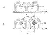
도 8은, 공통 전극(COML)과 터치 검출 전극(TDL) 사이의 프린지에 의한 전기력선을 모식적으로 도시하는 것으로, 도 8의 (A)는 공통 전극(COML)이 짧은 경우의 예(비교예)를 도시하고, 도 8의 (B)는 공통 전극(COML)이 긴 경우의 예(본 실시의 형태의 예)를 도시한다. 도 8은, 도 4에서, 터치 검출 기능이 있는 표시 장치(1)의 Ⅷ-Ⅷ화살로 본 방향의 단면도를 도시하고 있다.8A and 8B schematically show electric lines of force due to fringing between the common electrode COML and the touch detection electrode TDL. Fig. 8A shows a case where the common electrode COML is short (B) of FIG. 8 shows an example (an example of this embodiment) in which the common electrode COML is long. Fig. 8 shows a cross-sectional view of the
비교예에 관한 도 8의 (A)의 예에서는, 공통 전극(COML)은, 가장 외측의 터치 검출 전극(TDL)(도 8의 (A)의 왼쪽의 터치 검출 전극(TDL))의 중심으로부터, 터치 검출 전극(TDL)의 전극 피치(d)의 반분 미만에 대응하는 거리(de1)(<d/2)만큼 연신되어 있다. 한편, 본 실시의 형태에 관한 도 8의 (B)의 예에서는, 공통 전극(COML)은, 가장 외측의 터치 검출 전극(TDL)의 중심으로부터, 전극 피치(d)의 반분 이상에 대응하는 거리(de2)(≥d/2)만큼 연신되어 있다.In the example of Fig. 8A relating to the comparative example, the common electrode COML is connected to the center of the outermost touch detection electrode TDL (the left touch detection electrode TDL of Fig. 8A) (<D / 2) corresponding to less than half of the electrode pitch d of the touch detection electrode TDL. 8B according to the present embodiment, the common electrode COML has a distance from the center of the outermost touch detection electrode TDL to at least half of the electrode pitch d (de2) (? d / 2).
비교예에 관한 도 8의 (A)에서는, 공통 전극(COML)이 짧기 때문에, 이 가장 외측의 터치 검출 전극(TDL)의 프린지에 의한 전기력선은, 외측(부분(P1))에서 적게 되어 버린다. 즉, 이 가장 외측의 터치 검출 전극(TDL)의 프린지에 의한 전기력선의 수는, 다른 터치 검출 전극(TDL)의 것보다도 적게 되어 버린다. 이에 의해, 가장 외측의 터치 검출 전극(TDL)에 대응하는 영역에서의 검출 감도는, 다른 터치 검출 전극(TDL)에 대응하는 영역에서의 검출 감도에 비하여 낮게 되어 버린다.In Fig. 8A relating to the comparative example, since the common electrode COML is short, the electric line of force due to the fringing of the outermost touch detection electrode TDL becomes smaller at the outer side (portion P1). That is, the number of lines of electric force due to fringing of the outermost touch detection electrode TDL becomes smaller than that of the other touch detection electrodes TDL. As a result, the detection sensitivity in the region corresponding to the outermost touch detection electrode TDL becomes lower than the detection sensitivity in the region corresponding to the other touch detection electrode TDL.
한편, 본 실시의 형태에 관한 도 8의 (B)에서는, 공통 전극(COML)을 길게 함에 의해, 가장 외측의 터치 검출 전극(TDL)의 프린지에 의한 전기력선의 감소를 최소한으로 억제할 수 있다(부분(P2)). 이에 의해, 이 가장 외측의 터치 검출 전극(TDL)의 프린지에 의한 전기력선의 수를, 다른 터치 검출 전극(TDL)의 것과 동등하게 할 수 있고, 다른 터치 검출 전극(TDL)에 대응하는 영역에서의 검출 감도와 비교하고, 이 가장 외측의 터치 검출 전극(TDL)에 대응하는 영역에서의 검출 감도의 저하를 최소한으로 억제할 수 있다. 또한, 도 4에 도시한 바와 같이, 터치 검출 전극(TDL)을 유효 표시 영역(S) 내에 걸쳐서 병설하도록 하였기 때문에, 유효 표시 영역(S) 내에서, 터치에 대한 검출 감도를 균일하게 할 수 있다.On the other hand, in FIG. 8B according to the present embodiment, by decreasing the length of the common electrode COML, it is possible to minimize the reduction of the electric force lines due to fringing of the outermost touch detection electrode TDL ( Portion P2). This makes it possible to make the number of electric lines of force due to fringing of the outermost touch detection electrode TDL equal to that of the other touch detection electrodes TDL It is possible to reduce the detection sensitivity in the region corresponding to the outermost touch detection electrode TDL to a minimum. Further, as shown in Fig. 4, since the touch detection electrodes TDL are juxtaposed over the effective display area S, the detection sensitivity for touch can be made uniform in the effective display area S .
터치 검출 전극(TDL)과 FPC(5)를 통하여 접속된 터치 검출 회로에서는, 터치 검출 신호(Vdet)에 의거하여 터치의 검출이 행하여진다. 일반적으로, 터치 검출 회로는, 공급된 터치 검출 신호(Vdet)에 의거하여, 유효 표시 영역(S) 내에서 터치에 대한 검출 감도가 균일하게 되도록 보정 연산을 행하고, 그 연산 결과에 의거하여 터치 위치 등을 구한다. 터치 검출 기능이 있는 표시 장치(1)에서는, 상술한 바와 같이, 터치 검출 전극(TDL)을 연장시킴에 의해 검출 감도의 균일성을 개선하도록 하였기 때문에, 터치 검출 회로에서 보정 연산에 의한 보정량을 줄일 수 있고, 예를 들면 터치 위치의 검출 정밀도를 높일 수 있다.In the touch detection circuit connected to the touch detection electrode TDL via the
(효과)(effect)
이상과 같이, 본 실시의 형태에서는, 공통 전극을, 가장 외측의 터치 검출 전극의 중심으로부터, 터치 검출 전극의 전극 피치의 반분 이상에 대응하는 거리만큼 연신되도록 하였기 때문에, 이 가장 외측의 터치 검출 전극에 대응하는 영역에서의 검출 감도를, 보다 내측의 터치 검출 전극에 대응하는 영역에서의 검출 감도와 동등하게 할 수 있다.As described above, in the present embodiment, since the common electrode is extended from the center of the outermost touch detection electrode by a distance corresponding to at least half of the electrode pitch of the touch detection electrode, It is possible to make the detection sensitivity in the region corresponding to the inner touch detection electrode equal to the detection sensitivity in the region corresponding to the inner touch detection electrode.
또한, 본 실시의 형태에서는, 터치 검출 전극을 유효 표시 영역 내에 걸쳐서 병설하도록 하였기 때문에, 유효 표시 영역에서의 검출 감도의 균일성을 높일 수 있다. 또한, 이에 의해, 터치 검출 회로에서의 보정 연산에 의한 보정량을 줄일 수 있기 때문에, 예를 들면, 터치 위치의 검출 정밀도를 높일 수 있다.Further, in the present embodiment, since the touch detection electrodes are juxtaposed over the effective display region, the uniformity of the detection sensitivity in the effective display region can be enhanced. In this way, the amount of correction by the correction calculation in the touch detection circuit can be reduced, for example, so that the detection accuracy of the touch position can be enhanced.
[변형례 1][Modification 1]
상기 실시의 형태에서는, 공통 전극(COML) 및 터치 검출 전극(TDL)을 유효 표시 영역(S) 내에 걸쳐서 병설하였지만, 이것으로 한정되는 것이 아니고, 이에 대신하여, 예를 들면, 공통 전극(COML)을 유효 표시 영역(S) 밖에도 병설하여도 좋고, 터치 검출 전극(TDL)을 유효 표시 영역(S) 밖에도 병설하여도 좋다. 이하에, 공통 전극(COML) 및 터치 검출 전극(TDL)을 유효 표시 영역(S) 밖에 병설한 경우의 예를 나타낸다.Although the common electrode COML and the touch detection electrode TDL are disposed in the effective display region S within the effective display region S in the above embodiment, the common electrode COML is not limited thereto. Instead, for example, May be provided outside the effective display region (S), or the touch detection electrode (TDL) may be provided outside the effective display region (S). An example in which the common electrode COML and the touch detection electrode TDL are juxtaposed outside the effective display region S is shown below.
도 9는, 본 변형례에 관한 터치 검출 기능이 있는 표시 장치(1B)의 한 구성례를 도시하는 것이다. 도 9에 도시한 바와 같이, 공통 전극(COML)은, 유효 표시 영역(S)밖(도 9의 우단 및 좌단)에도 병설되어 있다. 터치 검출 전극(TDL)도 또한, 유효 표시 영역(S)밖(도 9의 상단 및 하단)에도 병설되어 있다. 또한, 터치 검출 전극(TDL)은, 유효 표시 영역(S)밖(도 9의 좌단)에서, 가장 외측의 공통 전극(COML)에 대응하는 위치까지 연신하여 형성되어 있다. 이에 의해, 터치 검출 기능이 있는 표시 장치(1B)에서는, 유효 표시 영역(S)에서 검출 감도를 균일하게 할 수 있음과 함께, 터치 검출 영역(St)을 유효 표시 영역(S)보다 넓게 할 수 있다.Fig. 9 shows an example of the configuration of the
<3. 제 2의 실시의 형태><3. Second Embodiment>
다음에, 본 발명의 제 2의 실시의 형태에 관한 터치 검출 기능이 있는 표시 장치(7)에 관해 설명한다. 본 실시의 형태는, 터치 검출 전극의 전극 피치(d)(배열 피치)가, 유효 표시 영역(S)에서 장소에 따라 다르도록 한 것이다. 그 밖의 구성은, 상기 제 1의 실시의 형태(도 4)와 마찬가지이다. 또한, 상기 제 1의 실시의 형태에 관한 터치 검출 기능이 있는 표시 장치(1)와 실질적으로 동일한 구성 부분에는 동일한 부호를 붙이고, 적절히 설명을 생략한다.Next, a
도 10은, 터치 검출 기능이 있는 표시 장치(7)의 한 구성례를 도시하는 것이다. 터치 검출 기능이 있는 표시 장치(7)에서, 터치 검출 전극(TDL)은, 도 10에 도시한 바와 같이, 그 전극 피치(d)가 장소에 따라 다르도록 병설되어 있다. 구체적으로는, 터치 검출 전극(TDL)은, 터치 검출 전극(TDL)의 연재 방향과 교차하는 방향에서, 유효 표시 영역(S)의 중앙 부근에서는 전극 피치(d)가 좁게 되도록 배치되고, 유효 표시 영역(S)의 단 부근에서는 전극 피치(d)가 넓게 되도록 배치되어 있다. 또한, 터치 검출 전극(TDL)의 배치는, 이것으로 한정되는 것이 아니고, 예를 들면, 터치 검출 전극(TDL)의 연재 방향과 교차하는 방향에서, 가장 외측의 터치 검출 전극(TDL)만, 전극 피치(d)가 넓게 되도록 하여도 좋다.Fig. 10 shows an example of the configuration of the
도 11은, 터치 검출 전극(TDL)의 전극 피치(d)를 바꾼 때의 프린지에 의한 전기력선의 변화를 모식적으로 도시하는 것이고, 도 11의 (A)는 전극 피치(d)가 좁은 경우(전극 피치(d1))를 도시하고, 도 11의 (B)는 전극 피치(d)가 넓은 경우(전극 피치(d2))를 도시한다. 이 도 11은, 설명의 편의상, 터치 검출 전극(TDL)이 2개만 병설된 경우를 나타내고 있다. 도 11에 도시한 바와 같이, 전극 피치(d)를 넓게 하면, 프린지에 의한 전기력선의 갯수가 증가한다(부분(P3)). 이에 의해, 그 전기력선이 증가한 터치 검출 전극(TDL)에 대응하는 영역에서의 검출 감도를 높일 수 있다.11A and 11B schematically show a change in the electric force line due to fringing when the electrode pitch d of the touch detection electrode TDL is changed. FIG. 11A shows a case where the electrode pitch d is narrow (Electrode pitch d1), and Fig. 11 (B) shows a case where the electrode pitch d is wide (electrode pitch d2). 11 shows a case where only two touch detection electrodes TDL are juxtaposed for convenience of explanation. As shown in Fig. 11, when the electrode pitch d is increased, the number of electric lines of force due to fringe is increased (portion P3). This makes it possible to increase the detection sensitivity in the region corresponding to the touch detection electrode TDL in which the electric line of force is increased.
도 12는, 전극 피치(d)와 검출 감도(Sens)와의 관계의 시뮬레이션 결과를 도시하는 것이다. 전극 피치(d)가 어느 값(전극 피치(da)) 이하인 경우에는, 도 12에 도시한 바와 같이, 전극 피치(d)가 넓게 됨과 함께, 검출 감도(Sens)는 높아진다. 여기서, 예를 들면, 터치 검출 전극(TDL)의 전극 폭(w)이 1㎜인 경우에 있어서, 전극 피치(da)는 3㎜ 정도이다. 이와 같이, 전극 피치의 범위(d<da)에서 전극 피치(d)를 변화시킴에 의해 검출 감도(Sens)를 조정할 수 있다.Fig. 12 shows a simulation result of the relationship between the electrode pitch d and the detection sensitivity (Sens). When the electrode pitch d is less than a certain value (the electrode pitch da), the electrode pitch d is increased and the detection sensitivity (Sens) is increased as shown in Fig. Here, for example, when the electrode width w of the touch detection electrode TDL is 1 mm, the electrode pitch da is about 3 mm. Thus, the detection sensitivity (Sens) can be adjusted by changing the electrode pitch d in the range of the electrode pitch (d <da).
도 10에 도시한 바와 같이, 터치 검출 기능이 있는 표시 장치(7)에서는, 유효 표시 영역(S)의 중앙 부근에서는 전극 피치(d)가 좁게 되도록 터치 검출 전극(TDL)을 배치하고, 유효 표시 영역(S)의 단 부근에서는 전극 피치(d)가 넓게 되도록 터치 검출 전극(TDL)을 배치하고 있다. 이에 의해, 예를 들면, 터치 검출 전극(TDL)을 일정한 전극 피치(d)로 형성한 경우에 있어서, 유효 표시 영역(S)의 단 부근에서 검출 감도(Sens)가 낮아진 때는, 그 단 부근에 배치된 터치 검출 전극(TDL)의 전극 피치(d)를 넓게 함에 의해, 그 터치 검출 전극(TDL)에 대응하는 영역의 검출 감도(Sens)를 높일 수 있고, 유효 표시 영역(S)에서의 검출 감도(Sens)를 균일하게 할 수 있다.10, in the
또한, 터치 검출 기능이 있는 표시 장치(7)에서는, 터치 검출 전극(TDL)의 전극 피치가 장소에 따라 다르기 때문에, 터치 검출 회로에서는, 이 전극 배치를 고려하여 좌표 보간을 행함에 의해 터치 위치를 구할 필요가 있다.In the
이상과 같이, 본 실시의 형태에서는, 터치 검출 전극의 전극 피치가 장소에 따라 다르도록 하였기 때문에, 터치 검출 전극에 교차하는 방향에서, 검출 감도를 자유롭게 설정할 수 있다.As described above, in the present embodiment, since the electrode pitch of the touch detection electrode is varied depending on the location, the detection sensitivity can be set freely in the direction crossing the touch detection electrode.
또한, 본 실시의 형태에서는, 유효 표시 영역 내에서, 외측에 배치한 터치 검출 전극의 전극 피치를, 보다 내측에 배치한 터치 검출 전극의 전극 피치와 같게 또는 넓게 하였기 때문에, 유효 표시 영역에서의 검출 감도의 균일성을 높일 수 있다. 또한, 이에 의해, 터치 검출 회로에서의 보정 연산에 의한 보정량을 줄일 수 있기 때문에, 예를 들면, 터치 위치의 검출 정밀도를 높일 수 있다.Further, in the present embodiment, since the electrode pitch of the touch detection electrodes arranged on the outer side in the effective display area is made equal to or wider than the electrode pitch of the touch detection electrodes arranged on the inner side, The uniformity of the sensitivity can be increased. In this way, the amount of correction by the correction calculation in the touch detection circuit can be reduced, for example, so that the detection accuracy of the touch position can be enhanced.
그 밖의 효과는, 상기 제 1의 실시의 형태의 경우와 마찬가지이다.The other effects are the same as in the case of the first embodiment.
<4. 제 3의 실시의 형태><4. Third Embodiment>
다음에, 본 발명의 제 3의 실시의 형태에 관한 터치 검출 기능이 있는 표시 장치(8)에 관해 설명한다. 본 실시의 형태는, 터치 검출 전극의 전극 폭이, 유효 표시 영역(S)에서의 장소에 따라 다르도록 한 것이다. 그 밖의 구성은, 상기 제 1의 실시의 형태(도 4)와 마찬가지이다. 또한, 상기 제 1의 실시의 형태에 관한 터치 검출 기능이 있는 표시 장치(1)와 실질적으로 동일한 구성 부분에는 동일한 부호를 붙이고, 적절히 설명을 생략한다.Next, a
도 13은, 터치 검출 기능이 있는 표시 장치(8)의 한 구성례를 도시하는 것이다. 터치 검출 기능이 있는 표시 장치(8)에서, 터치 검출 전극(TDL)은, 도 13에 도시한 바와 같이, 그 전극 폭(w)이 장소에 따라 다르도록 형성되어 있다. 구체적으로는, 터치 검출 전극(TDL)은, 터치 검출 전극(TDL)의 연재 방향과 교차하는 방향에서, 유효 표시 영역(S)의 중앙 부근에서는 전극 폭(w)이 넓게 되도록 형성되고, 유효 표시 영역(S)의 단 부근에서는 전극 폭(w)이 좁게 되도록 형성되어 있다. 또한, 터치 검출 전극(TDL)의 폭은, 이것으로 한정되는 것이 아니고, 예를 들면, 터치 검출 전극(TDL)의 연재 방향과 교차하는 방향에서, 가장 외측의 터치 검출 전극(TDL)만, 그 전극 폭(w)이 좁게 되도록 하여도 좋다.Fig. 13 shows an example of the configuration of the
도 14는, 터치 검출 전극(TDL)의 전극 폭(w)을 바꾼 때의 프린지에 의한 전기력선의 변화를 모식적으로 도시하는 것이고, 도 14의 (A)는 전극 폭(w)이 넓은 경우(전극 폭(w2))을 도시하고, 도 14의 (B)는 전극 폭(w)이 좁은 경우(전극 폭(w1))을 도시한다. 도 14는, 설명의 편의상, 터치 검출 전극(TDL)이 2개만 병설된 경우를 나타내고 있다. 도 14에 도시한 바와 같이, 전극 폭(w)을 좁게 하면, 전기력선의 갯수가 증가한다(부분(P4)). 이에 의해, 그 전기력선이 증가한 터치 검출 전극(TDL)에 대응하는 영역에서의 검출 감도를 높일 수 있다.Fig. 14 schematically shows a change in the electric force line due to fringing when the electrode width w of the touch detection electrode TDL is changed. Fig. 14 (A) shows a case where the electrode width w is wide Electrode width w2), and Fig. 14 (B) shows a case where the electrode width w is narrow (electrode width w1). Fig. 14 shows a case where only two touch detection electrodes TDL are juxtaposed for convenience of explanation. As shown in Fig. 14, when the electrode width w is narrowed, the number of electric lines of force increases (portion P4). This makes it possible to increase the detection sensitivity in the region corresponding to the touch detection electrode TDL in which the electric line of force is increased.
도 15는, 전극 폭(w)과 검출 감도(Sens)와의 관계의 시뮬레이션 결과를 도시하는 것이다. 도 15에 도시한 바와 같이, 검출 감도(Sens)는, 전극 폭(wa)일 때에 최대로 되고, 그 전극 폭으로부터 떨어짐에 따라 저하된다. 여기서, 예를 들면, 터치 검출 전극(TDL)의 전극 피치(d)가 5㎜인 경우에는, 이 전극 폭(wa)은 1㎜ 정도이다. 이 도 15의 우측에서, 전극 폭(w)이 전극 폭(wa)보다도 넓게 되면 검출 감도(Sens)가 저하되는 것은, 상술한 바와 같이, 전극 폭(w)이 넓게 됨에 의해 프린지에 의한 전기력선이 감소하기 때문이다. 한편, 이 도 15의 좌측에 도시한 바와 같이, 전극 폭(w)이 전극 폭(wa)보다도 좁게 됨에 의해 검출 감도(Sens)가 저하되는 것은, 전극 폭(w)이 좁게 됨에 의해 터치 검출 전극(TDL)의 저항치가 커지고 시정수가 커지기 때문에, 터치 검출 신호(Vdet)가 터치 검출 전극(TDL)을 통과하여 터치 검출 회로에 전해지기 어려워지는 것에 기인하고 있다. 이와 같이, 전극 폭(w)을 변화시킴에 의해, 검출 감도(Sens)을 조정할 수 있다.Fig. 15 shows the simulation result of the relationship between the electrode width w and the detection sensitivity (Sens). As shown in Fig. 15, the detection sensitivity (Sens) becomes maximum when the electrode width wa is reached, and decreases with the distance from the electrode width. Here, for example, when the electrode pitch d of the touch detection electrode TDL is 5 mm, the electrode width wa is about 1 mm. 15, when the electrode width w is wider than the electrode width wa, the detection sensitivity (Sens) is lowered because the electrode width w is widened as described above, . On the other hand, as shown in the left side of Fig. 15, the detection sensitivity (Sens) is lowered because the electrode width w is narrower than the electrode width wa because the electrode width w is narrow, The resistance value of the touch detection signal TDL is increased and the time constant is increased. This is because the touch detection signal Vdet is hardly transmitted to the touch detection circuit through the touch detection electrode TDL. Thus, the detection sensitivity (Sens) can be adjusted by changing the electrode width w.
도 13에 도시한 바와 같이, 터치 검출 기능이 있는 표시 장치(8)에서는, 유효 표시 영역(S)의 중앙 부근에서는 전극 폭(w)이 넓게 되도록 터치 검출 전극(TDL)을 배치하고, 유효 표시 영역(S)의 단 부근에서는 전극 폭(w)이 좁게 되도록 터치 검출 전극(TDL)을 배치하고 있다. 이에 의해, 예를 들면, 도 15에 도시한 바와 같이, 터치 검출 전극(TDL)을, 유효 표시 영역(S) 내에서 일정한 넓은 전극 폭(w2)로 형성하는 경우에 있어서, 유효 표시 영역(S)의 단 부근에서 검출 감도(Sens)가 낮아진 때는, 그 단 부근에 배치된 터치 검출 전극(TDL)의 전극 폭(w1)과 같이 좁게 함에 의해, 그 터치 검출 전극(TDL)에 대응하는 영역의 검출 감도(Sens)를 높일 수 있고, 유효 표시 영역(S)에서의 검출 감도(Sens)를 균일하게 할 수 있다.13, in the
이상과 같이, 본 실시의 형태에서는, 터치 검출 전극의 전극 폭이 각각 다르도록 하였기 때문에, 터치 검출 전극에 교차하는 방향에서, 검출 감도를 자유롭게 설정할 수 있다.As described above, in the present embodiment, since the electrode widths of the touch detection electrodes are set to be different from each other, the detection sensitivity can be freely set in the direction crossing the touch detection electrodes.
또한, 본 실시의 형태에서는, 유효 표시 영역 내에서, 외측에 배치한 터치 검출 전극의 전극 폭을, 보다 내측에 배치한 터치 검출 전극의 전극 폭과 같게 또는 좁게 하였기 때문에, 유효 표시 영역에서의 검출 감도의 균일성을 높일 수 있다. 또한, 이에 의해, 터치 검출 회로에서의 보정 연산에 의한 보정량을 줄일 수 있기 때문에, 예를 들면, 터치 위치의 검출 정밀도를 높일 수 있다.Further, in the present embodiment, since the electrode width of the touch detection electrode disposed on the outer side in the effective display region is made equal to or narrower than the electrode width of the touch detection electrode disposed on the inner side, The uniformity of the sensitivity can be increased. In this way, the amount of correction by the correction calculation in the touch detection circuit can be reduced, for example, so that the detection accuracy of the touch position can be enhanced.
그 밖의 효과는, 상기 제 1의 실시의 형태의 경우와 마찬가지이다.The other effects are the same as in the case of the first embodiment.
<5. 제 4의 실시의 형태><5. Fourth Embodiment >
다음에, 본 발명의 제 4의 실시의 형태에 관한 터치 검출 기능이 있는 표시 장치(9)에 관해 설명한다. 본 실시의 형태는, 표면 유리판의 두께가, 유효 표시 영역(S)에서의 장소에 따라 다르도록 한 것이다. 그 밖의 구성은 상기 제 1의 실시의 형태(도 4)와 마찬가지이다. 또한, 상기 제 1의 실시의 형태에 관한 터치 검출 기능이 있는 표시 장치(1)와 실질적으로 동일한 구성 부분에는 동일한 부호를 붙이고, 적절히 설명을 생략한다.Next, a
도 16은, 터치 검출 기능이 있는 표시 장치(9)의 한 구성례를 도시하는 것이다. 터치 검출 기능이 있는 표시 장치(9)에서, 표면 유리판(36)은, 도 16에 도시한 바와 같이, 그 두께가 장소에 따라 다르도록 형성되어 있다. 구체적으로는, 표면 유리판(36)은, 터치 검출 전극(TDL)의 연재 방향과 교차하는 방향에서, 유효 표시 영역(S)의 중앙 부근에서는 두껍게 되도록 형성되고, 유효 표시 영역(S)의 단 부근에서는 얇게 되도록 형성되어 있다.Fig. 16 shows an example of the configuration of the
도 17은, 표면 유리판(36)의 두께를 바꾼 때의 프린지에 의한 전기력선의 변화를 모식적으로 도시하는 것이고, (A)는 표면 유리판(36)이 두꺼운 경우를 도시하고, (B)는 얇은 경우를 도시한다. 도 17에 도시한 바와 같이, 표면 유리판을 얇게 하면, 손가락 등이 터치한 때에 그 손가락이 프린지에 의한 많은 수의 전기력선을 차단하게 된다(부분(P5)). 이에 의해, 그 전기력선이 차단된 터치 검출 전극(TDL)에 대응하는 영역에서의 터치의 검출 감도를 높일 수 있다.17A and 17B schematically show a change in the electric force line due to fringing when the thickness of the
도 16에 도시한 바와 같이, 터치 검출 기능이 있는 표시 장치(9)에서는, 유효 표시 영역(S)의 중앙 부근에서는 표면 유리판(36)을 두껍게 형성하고, 유효 표시 영역(S)의 단 부근에서는 얇게 형성하고 있다. 이에 의해, 예를 들면, 표면 유리판(36)의 두께를 유효 표시 영역(S)에서 일정하게 하여 형성한 경우에 있어서, 유효 표시 영역(S)의 단 부근에서 검출 감도(Sens)가 낮아진 때는, 그단 부근의 표면 유리판(36)을 얇게 함에 의해, 그 부분의 검출 감도(Sens)를 높일 수 있고, 유효 표시 영역(S)에서의 검출 감도(Sens)를 균일하게 할 수 있다.16, in the
이상과 같이, 본 실시의 형태에서는, 표면 유리판의 두께를 장소에 따라 다르도록 하였기 때문에, 검출 감도를 자유롭게 설정할 수 있다.As described above, in this embodiment, since the thickness of the surface glass plate is varied depending on the place, the detection sensitivity can be freely set.
또한, 본 실시의 형태에서는, 유효 표시 영역 내의, 터치 검출 전극에 교차하는 방향에서, 외측의 표면 유리판의 두께를, 보다 내측의 두께와 같게 또는 얇게 하였기 때문에, 유효 표시 영역에서의 검출 감도의 균일성을 높일 수 있다. 또한, 이에 의해, 터치 검출 회로에서의 보정 연산에 의한 보정량을 줄일 수 있기 때문에, 예를 들면, 터치 위치의 검출 정밀도를 높일 수 있다.In the present embodiment, since the thickness of the outer surface glass plate in the effective display area crosses the touch detection electrode is made equal to or thinner than the inner thickness, the uniformity of the detection sensitivity in the effective display area You can increase your sex. In this way, the amount of correction by the correction calculation in the touch detection circuit can be reduced, for example, so that the detection accuracy of the touch position can be enhanced.
그 밖의 효과는, 상기 제 1의 실시의 형태의 경우와 마찬가지이다.The other effects are the same as in the case of the first embodiment.
이상, 터치 검출 기능이 있는 표시 장치를 예로 실시의 형태를 설명하였지만, 이것으로 한정되는 것이 아니고, 예를 들면, 단일의 터치 검출 장치로 실시하여도 좋다. 이하에, 그 경우의 예에 관해 설명한다.The embodiment has been described above with reference to a display device having a touch detection function. However, the present invention is not limited to this. For example, a single touch detection device may be used. Hereinafter, an example of such a case will be described.
<6. 제 5의 실시의 형태><6. Fifth Embodiment>
다음에, 본 발명의 제 5의 실시의 형태에 관한 터치 검출 장치(17)에 관해 설명한다. 본 실시의 형태는, 상기 제 2의 실시의 형태에 관한 터치 검출 기능이 있는 표시 장치(7)의 주요부를 단일의 터치 검출 장치에 적용한 것이고, 터치 검출 전극의 전극 피치(d)가 장소에 따라 다르도록 한 것이다. 또한, 상기 제 2의 실시의 형태에 관한 터치 검출 기능이 있는 표시 장치(7)(도 10)와 실질적으로 동일한 구성 부분에는 동일한 부호를 붙이고, 적절히 설명을 생략한다.Next, the
도 18은, 터치 검출 장치(17)의 한 구성례를 도시하는 것이다. 터치 검출 장치(17)는, 유리 기판(37)과, 구동 전극(40)을 구비하고 있다. 구동 전극(40)은, 상술한 정전용량식 터치 검출의 기본 원리에서의 구동 전극(E1)에 대응하는 것이고, 상기 제 2의 실시의 형태 등에서의 공통 전극(COML)에 대응하는 것이다. 유리 기판(37)의 한쪽의 면에는 구동 전극(40)이 병설되고, 다른쪽의 면에는, 구동 전극(40)과 교차하는 방향에 터치 검출 전극(TDL)이 병설되어 있다. 터치 검출 전극(TDL)은, 상기 제 2의 실시의 형태에 관한 터치 검출 기능이 있는 표시 장치(7)의 경우와 마찬가지로, 그 전극 피치(d)가 다르도록 병설되어 있다. 구체적으로는, 터치 검출 전극(TDL)은, 터치 검출 전극(TDL)의 연재 방향과 교차하는 방향에서, 터치 검출 장치(17)의 중앙 부근에서는 전극 피치(d)가 좁게 되도록 배치되고, 단 부근에서는 전극 피치(d)가 넓게 되도록 배치되어 있다. 이에 의해, 상기 제 2의 실시의 형태의 경우와 완전히 마찬가지로, 터치에 대한 검출 감도(Sens)를 균일하게 할 수 있다.Fig. 18 shows an example of the configuration of the
이상과 같이, 본 실시의 형태에서는, 터치 검출 전극의 전극 피치가 각각 다르도록 하였기 때문에, 터치 검출 전극에 교차하는 방향에서, 검출 감도를 자유롭게 설정할 수 있다.As described above, in the present embodiment, since the electrode pitches of the touch detection electrodes are different from each other, the detection sensitivity can be freely set in the direction crossing the touch detection electrodes.
또한, 본 실시의 형태에서는, 외측에 배치한 터치 검출 전극의 전극 피치를, 보다 내측에 배치한 터치 검출 전극의 전극 피치와 같게 또는 크게 하였기 때문에, 검출 감도의 균일성을 높일 수 있다. 또한, 이에 의해, 터치 검출 회로에서의 보정 연산에 의한 보정량을 줄일 수 있기 때문에, 예를 들면, 터치 위치의 검출 정밀도를 높일 수 있다.Further, in the present embodiment, the electrode pitch of the touch detection electrodes disposed outside is made equal to or larger than the electrode pitch of the touch detection electrodes disposed further inside, so that the uniformity of the detection sensitivity can be enhanced. In this way, the amount of correction by the correction calculation in the touch detection circuit can be reduced, for example, so that the detection accuracy of the touch position can be enhanced.
<7. 제 6의 실시의 형태><7. Sixth Embodiment>
다음에, 본 발명의 제 6의 실시의 형태에 관한 터치 검출 장치(18)에 관해 설명한다. 본 실시의 형태는, 상기 제 3의 실시의 형태에 관한 터치 검출 기능이 있는 표시 장치(8)의 주요부를 터치 검출 장치 단체에 적용한 것이고, 터치 검출 전극의 전극 폭(w)이 장소에 따라 다르도록 한 것이다. 또한, 상기 제 3의 실시의 형태에 관한 터치 검출 기능이 있는 표시 장치(8)와 실질적으로 동일한 구성 부분에는 동일한 부호를 붙이고, 적절히 설명을 생략한다.Next, the
도 19는, 터치 검출 장치(18)의 한 구성례를 도시하는 것이다. 터치 검출 전극(TDL)은, 상기 제 3의 실시의 형태에 관한 터치 검출 기능이 있는 표시 장치(8)의 경우와 마찬가지로, 그 전극 폭(w)이 장소에 따라 다르도록 형성되어 있다. 구체적으로는, 터치 검출 전극(TDL)은, 터치 검출 전극(TDL)의 연재 방향과 교차하는 방향에서, 터치 검출 장치(18)의 중앙 부근에서는 전극 폭(w)이 넓게 되도록 형성되고, 단 부근에서는 전극 폭(w)이 좁게 되도록 형성되어 있다. 이에 의해, 상기 제 3의 실시의 형태의 경우와 완전히 마찬가지로, 터치에 대한 검출 감도(Sens)를 균일하게 할 수 있다.Fig. 19 shows an example of the configuration of the
이상과 같이, 본 실시의 형태에서는, 터치 검출 전극의 전극 폭이 각각 다르도록 하였기 때문에, 터치 검출 전극에 교차하는 방향에서, 검출 감도를 자유롭게 설정할 수 있다.As described above, in the present embodiment, since the electrode widths of the touch detection electrodes are set to be different from each other, the detection sensitivity can be freely set in the direction crossing the touch detection electrodes.
또한, 본 실시의 형태에서는, 외측에 배치한 터치 검출 전극의 전극 폭을, 보다 내측에 배치한 전극 폭과 같게 또는 좁게 하였기 때문에, 검출 감도의 균일성을 높일 수 있다. 또한, 이에 의해, 터치 검출 회로에서의 보정 연산에 의한 보정량을 줄일 수 있기 때문에, 예를 들면, 터치 위치의 검출 정밀도를 높일 수 있다.Further, in the present embodiment, the electrode width of the touch detection electrode disposed outside is made equal to or narrower than the electrode width arranged inside, thereby improving the uniformity of the detection sensitivity. In this way, the amount of correction by the correction calculation in the touch detection circuit can be reduced, for example, so that the detection accuracy of the touch position can be enhanced.
<8. 제 7의 실시의 형태><8. Seventh Embodiment >
다음에, 본 발명의 제 7의 실시의 형태에 관한 터치 검출 장치(19)에 관해 설명한다. 본 실시의 형태는, 상기 제 4의 실시의 형태에 관한 터치 검출 기능이 있는 표시 장치(9)의 주요부를 터치 검출 장치 단체에 적용한 것이고, 표면 유리판의 두께가 장소에 따라 다르도록 한 것이다. 또한, 상기 제 4의 실시의 형태에 관한 터치 검출 기능이 있는 표시 장치(9)와 실질적으로 동일한 구성 부분에는 동일한 부호를 붙이고, 적절히 설명을 생략한다.Next, a
도 20은, 터치 검출 장치(19)의 한 구성례를 도시하는 것이다. 터치 검출 장치(19)는, 평탄화층(37)을 구비하고 있다. 평탄화층(37)은, 예를 들면 절연층, 보호막, 편광판 등을 사용 가능하다. 평탄화층(37)은, 유리 기판(37)에서의 터치 검출 전극(TDL)이 형성된 면에 형성된 것이고, 그 위에 표면 유리판(36)이 배치된다. 표면 유리판(36)은, 상기 제 4의 실시의 형태에 관한 터치 검출 기능이 있는 표시 장치(9)의 경우와 마찬가지로, 그 두께가 장소에 따라 다르도록 형성되어 있다. 구체적으로는, 표면 유리판(36)은, 터치 검출 전극(TDL)의 연재 방향과 교차하는 방향에서, 터치 검출 장치(19)의 중앙 부근에서는 두껍게 되도록 형성되고, 단 부근에서는 얇게 되도록 형성되어 있다. 이에 의해, 상기 제 4의 실시의 형태의 경우와 완전히 마찬가지로, 터치에 대한 검출 감도(Sens)를 균일하게 할 수 있다.Fig. 20 shows an example of the configuration of the
이상과 같이, 본 실시의 형태에서는, 표면 유리판의 두께를 장소에 따라 다르도록 하였기 때문에, 검출 감도를 자유롭게 설정할 수 있다.As described above, in this embodiment, since the thickness of the surface glass plate is varied depending on the place, the detection sensitivity can be freely set.
또한, 본 실시의 형태에서는, 터치 검출 전극에 교차하는 방향에서, 외측의 표면 유리판의 두께를, 보다 내측의 두께와 같게 또는 얇게 하였기 때문에, 검출 감도의 균일성을 높일 수 있다. 또한, 이에 의해, 터치 검출 회로에서의 보정 연산에 의한 보정량을 줄일 수 있기 때문에, 예를 들면, 터치 위치의 검출 정밀도를 높일 수 있다.Further, in the present embodiment, since the thickness of the outer surface glass plate in the direction crossing the touch detection electrode is made equal to or thinner than the inner thickness, the uniformity of the detection sensitivity can be increased. In this way, the amount of correction by the correction calculation in the touch detection circuit can be reduced, for example, so that the detection accuracy of the touch position can be enhanced.
<9. 적용례><9. Application>
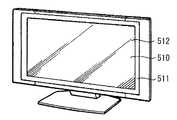
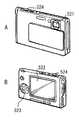
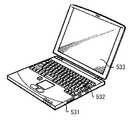
다음에, 도 21 내지 도 25를 참조하여, 상기 실시의 형태 및 변형례로 설명한 터치 검출 기능이 있는 표시 장치 및 터치 검출 장치의 적용례에 관해 설명한다. 상기 실시의 형태 등의 터치 검출 기능이 있는 표시 장치 등은, 텔레비전 장치, 디지털 카메라, 노트형 퍼스널 컴퓨터, 휴대 전화 등의 휴대 단말 장치 또는 비디오 카메라 등의 모든 분야의 전자 기기에 적용하는 것이 가능하다. 환언하면, 상기 실시의 형태 등의 터치 검출 기능이 있는 표시 장치 등은, 외부로부터 입력된 영상 신호 또는 내부에서 생성한 영상 신호를, 화상 또는 영상으로서 표시하는 모든 분야의 전자 기기에 적용하는 것이 가능하다.Next, an application example of the display device and the touch detection device having the touch detection function described in the above embodiments and modifications will be described with reference to Figs. 21 to 25. Fig. The display device having the touch detection function and the like in the above embodiments can be applied to electronic devices in all fields such as a television device, a digital camera, a portable terminal device such as a notebook type personal computer, a mobile phone, or a video camera . In other words, a display device or the like having a touch detection function, such as the above-described embodiment, can be applied to electronic devices in all fields that display a video signal input from the outside or a video signal generated internally as an image or an image Do.
(적용례 1)(Application example 1)
도 21은, 상기 실시의 형태 등의 터치 검출 기능이 있는 표시 장치 등이 적용되는 텔레비전 장치의 외관을 도시하는 것이다. 이 텔레비전 장치는, 예를 들면, 프런트 패널(511) 및 필터 유리(512)를 포함하는 영상 표시 화면부(510)를 갖고 있고, 이 영상 표시 화면부(510)는, 상기 실시의 형태 등에 관한 터치 검출 기능이 있는 표시 장치 등에 의해 구성되어 있다.Fig. 21 shows the appearance of a television apparatus to which a display device having a touch detection function or the like according to the above-described embodiments is applied. This television apparatus has, for example, a video
(적용례 2)(Application example 2)
도 22는, 상기 실시의 형태 등의 터치 검출 기능이 있는 표시 장치 등이 적용되는 디지털 카메라의 외관을 도시하는 것이다. 이 디지털 카메라는, 예를 들면, 플래시용의 발광부(521), 표시부(522), 메뉴 스위치(523) 및 셔터 버튼(524)을 갖고 있고, 그 표시부(522)는, 상기 실시의 형태 등에 관한 터치 검출 기능이 있는 표시 장치 등에 의해 구성되어 있다.Fig. 22 shows an appearance of a digital camera to which a display device having a touch detection function or the like according to the above-described embodiments is applied. This digital camera has a
(적용례 3)(Application example 3)
도 23은, 상기 실시의 형태 등의 터치 검출 기능이 있는 표시 장치 등이 적용되는 노트형 퍼스널 컴퓨터의 외관을 도시하는 것이다. 이 노트형 퍼스널 컴퓨터는, 예를 들면, 본체(531), 문자 등의 입력 조작을 위한 키보드(532) 및 화상을 표시하는 표시부(533)를 갖고 있고, 그 표시부(533)는, 상기 실시의 형태 등에 관한 터치 검출 기능이 있는 표시 장치 등에 의해 구성되어 있다.Fig. 23 shows an appearance of a notebook type personal computer to which a display device having a touch detection function or the like according to the above-described embodiments is applied. This notebook personal computer has, for example, a
(적용례 4)(Application example 4)
도 24는, 상기 실시의 형태 등의 터치 검출 기능이 있는 표시 장치 등이 적용되는 비디오 카메라의 외관을 도시하는 것이다. 이 비디오 카메라는, 예를 들면, 본체부(541), 이 본체부(541)의 전방 측면에 마련된 피사체 촬영용의 렌즈(542), 촬영시의 스타트/스톱 스위치(543) 및 표시부(544)를 갖고 있다. 그리고 그 표시부(544)는, 상기 실시의 형태 등에 관한 터치 검출 기능이 있는 표시 장치 등에 의해 구성되어 있다.Fig. 24 shows an appearance of a video camera to which a display device having a touch detection function or the like according to the above-described embodiments is applied. The video camera includes, for example, a
(적용례 5)(Application example 5)
도 25는, 상기 실시의 형태 등의 터치 검출 기능이 있는 표시 장치 등이 적용되는 휴대 전화기의 외관을 도시하는 것이다. 이 휴대 전화기는, 예를 들면, 상측 몸체(710)와 하측 몸체(720)를 연결부(힌지부)(730)로 연결한 것이고, 디스플레이(740), 서브 디스플레이(750), 픽처 라이트(760) 및 카메라(770)를 갖고 있다. 그 디스플레이(740) 또는 서브 디스플레이(750)는, 상기 실시의 형태 등에 관한 터치 검출 기능이 있는 표시 장치 등에 의해 구성되어 있다.Fig. 25 shows an appearance of a mobile phone to which a display device having a touch detection function or the like according to the above-described embodiments is applied. The
이상, 몇 가지의 실시의 형태 및 변형례, 및 전자 기기에의 적용례를 들어 본 발명을 설명하였지만, 본 발명은 이들의 실시의 형태 등으로는 한정되지 않고, 여러가지의 변형이 가능하다.While the present invention has been described with reference to several embodiments and modifications and application examples to electronic apparatuses, the present invention is not limited to these embodiments, and various modifications are possible.
예를 들면, 상기 제 1 내지 제 4의 실시의 형태 등에서는, FFS나 IPS 등의 횡전계 모드의 액정을 이용한 액정 표시 디바이스와 터치 검출 디바이스를 일체화하였지만, 이것에 대신하여, TN(트위스티드 네마틱), VA(수직 배향), ECB(전계 제어 복굴절) 등의 각종 모드의 액정을 이용한 액정 표시 디바이스와 터치 검출 디바이스를 일체화하여도 좋다. 이와 같은 액정을 이용한 경우에는, 터치 검출 기능이 있는 표시 장치를, 도 26에 제한 표지한 대로 구성 가능하다. 도 26은, 본 변형례에 관한 터치 검출 기능이 있는 표시 장치의 주요부 단면 구조의 한 예를 도시하는 것이고, 화소 기판(2B)과 대향 기판(3B)의 사이에 액정층(6B)이 협지된 상태를 나타내고 있다. 그 밖의 각 부분의 명칭이나 기능 등은 도 5의 경우와 마찬가지이므로 설명을 생략한다. 이 예에서는, 도 5의 경우와는 달리, 표시용과 터치 검출용의 쌍방에 겸용된 공통 전극(COML)은, 대향 기판(3B)에 형성되어 있다.For example, in the first to fourth embodiments described above, the liquid crystal display device using the liquid crystal of the transverse electric field mode such as FFS or IPS is integrated with the touch detection device. However, in place of the TN, ), VA (vertical alignment), ECB (electric field control birefringence), and the like may be integrated with the liquid crystal display device using the liquid crystal. In the case of using such a liquid crystal, a display device having a touch detection function can be configured as shown in Fig. 26 shows an example of a sectional structure of a main part of a display device having a touch detection function according to the present modification. In the display device in which the
또한, 예를 들면, 제 2 내지 제 4의 실시의 형태에 관한 터치 검출 기능이 있는 표시 장치(7 내지 9)를 조합시켜도 좋다. 구체적으로는, 예를 들면, 터치 검출 전극(TDL)의 전극 피치(d) 및 전극 폭(w)의 양쪽이, 유효 표시 영역(S)에서 다르도록 하여도 좋고, 터치 검출 전극(TDL)의 전극 피치(d)가 유효 표시 영역(S)에서 다르도록 하면서, 표면 유리판의 두께가 장소에 따라 다르도록 하여도 좋고, 터치 검출 전극(TDL)의 전극 폭(w)이 다르도록 하면서 표면 유리판의 두께가 장소에 따라 다르도록 하여도 좋다. 또한, 예를 들면, 터치 검출 전극(TDL)의 전극 피치(d) 및 전극 폭(w)의 양쪽이 유효 표시 영역(S)에서 다르도록 하면서, 표면 유리판의 두께가 장소에 따라 다르도록 하여도 좋다. 마찬가지로, 제 5 내지 제 7의 실시의 형태에 관한 터치 검출 장치(17 내지 19)를 조합시켜도 좋다.Further, for example, the
1, 1B, 7, 8, 9 : 터치 검출 기능이 있는 표시 장치
2, 2B : 화소 기판
3, 3B : 대향 기판
4 : 실
5 : FPC
6, 6B : 액정층
21 : TFT 기판
22 : 화소 전극
23 : 절연층
31, 37 : 유리 기판
32 : 컬러 필터
35 : 편광판
36 : 표면 유리판
38 : 평탄화층
40 : 구동 전극
COML : 공통 전극
d : 전극 피치
GCL : 주사 신호선
LC : 액정 소자
S : 유효 표시 영역
Sens : 검출 감도
St : 터치 검출 영역
SGL : 화소 신호선
Pix : 화소
TDL : 터치 검출 전극
Tr : TFT 소자
Vdet : 터치 검출 신호
w : 전극 폭1, 1B, 7, 8, 9: Display device with touch detection function
2, 2B: pixel substrate
3, 3B: opposing substrate
4: Room
5: FPC
6, 6B: liquid crystal layer
21: TFT substrate
22:
23: Insulating layer
31, 37: glass substrate
32: Color filter
35: polarizer
36: Surface glass plate
38: planarization layer
40: driving electrode
COML: common electrode
d: electrode pitch
GCL: scan signal line
LC: liquid crystal element
S: Effective display area
Sens: Detection sensitivity
St: Touch detection area
SGL: a pixel signal line
Pix: Pixel
TDL: touch detection electrode
Tr: TFT element
Vdet: touch detection signal
w: electrode width
Claims (21)
Translated fromKorean제 1의 방향으로 연재되도록 병설된 복수의 터치 검출 전극과,
상기 제 1의 방향과 교차하는 제 2의 방향으로 연재되도록 병설되고, 상기 터치 검출 전극과 구동 전극의 교차 부분에 정전용량을 형성하는 복수의 구동 전극을 구비하고,
상기 복수의 구동 전극이, 상기 표시 기능층의 유효 표시 영역에 배치된 터치 검출 전극 중의 가장 외측에 위치하는 터치 검출 전극의 중심과 상기 가장 외측에 위치하는 터치 검출 전극의 내측에 위치한 터치 검출 전극의 중심의 피치의 반이거나 또는 반 이상의 거리만큼 떨어진 제 1의 위치 또는 그 외측의 제 2의 위치까지 연신하고,
상기 유효 표시 영역의 외연이 상기 제 1의 위치 또는 그 내측에 있는 것을 특징으로 하는 터치 검출 기능이 있는 표시 장치.A display function layer,
A plurality of touch detection electrodes juxtaposed in a first direction,
And a plurality of driving electrodes which are juxtaposed in a second direction intersecting with the first direction and which form an electrostatic capacitance at an intersection of the touch detection electrode and the driving electrode,
Wherein the plurality of driving electrodes are disposed on the outer side of the center of the touch detection electrode located at the outermost one of the touch detection electrodes disposed in the effective display region of the display function layer and the center of the touch detection electrode located inside the outermost touch detection electrode Stretching to a first position spaced apart by half or more than half the pitch of the center or to a second position outside thereof,
Wherein an outline of the effective display area is located at the first position or inside thereof.
상기 복수의 구동 전극은, 상기 제 1의 방향에서의 상기 유효 표시 영역의 외측에 병설된 하나 이상의 구동 전극도 포함하는 것을 특징으로 하는 터치 검출 기능이 있는 표시 장치.The method according to claim 1,
Wherein the plurality of driving electrodes include at least one driving electrode provided outside the effective display region in the first direction.
상기 복수의 터치 검출 전극은, 상기 제 2의 방향에서의 상기 유효 표시 영역의 외측에 병설된 하나 이상의 터치 검출 전극도 포함하고, 적어도 가장 외측의 구동 전극의 외측에 위치한 제 3의 위치까지 연신되어 있는 것을 특징으로 하는 터치 검출 기능이 있는 표시 장치.The method according to claim 1,
The plurality of touch detection electrodes may include at least one touch detection electrode provided outside the effective display area in the second direction and may extend to a third position located at least outside the most outer drive electrode Wherein the display device has a touch detection function.
상기 복수의 터치 검출 전극은, 서로 같은 전극 폭으로 형성되고,
외측에 배치된 터치 검출 전극의 배열 피치는, 상기 유효 표시 영역 내에서, 내측에 배치된 터치 검출 전극의 배열 피치보다도 넓게 되어 있는 것을 특징으로 하는 터치 검출 기능이 있는 표시 장치.The method according to claim 1,
Wherein the plurality of touch detection electrodes are formed to have the same electrode width,
And the arrangement pitch of the touch detection electrodes disposed on the outside is wider than the arrangement pitch of the touch detection electrodes disposed on the inside in the effective display area.
상기 복수의 터치 검출 전극은, 서로 같은 배열 피치로 배치되고,
외측에 배치된 터치 검출 전극의 전극 폭은, 상기 유효 표시 영역 내에서, 내측에 배치된 터치 검출 전극의 전극 폭보다도 좁게 되어 있는 것을 특징으로 하는 터치 검출 기능이 있는 표시 장치.The method according to claim 1,
Wherein the plurality of touch detection electrodes are arranged at the same pitch,
Wherein the electrode width of the touch detection electrode disposed on the outer side is narrower than the electrode width of the touch detection electrode disposed on the inner side in the effective display region.
상기 복수의 터치 검출 전극의 위에, 적어도 상기 유효 표시 영역을 덮도록 형성된 표면층을 또한 구비하고, 상기 제 2의 방향에서 외측에 배치된 상기 표면층의 두께는, 상기 제 2의 방향에서 내측에 배치된 상기 표면층의 두께보다도 얇게 되어 있는 것을 특징으로 하는 터치 검출 기능이 있는 표시 장치.The method according to claim 1,
And a surface layer formed so as to cover at least the effective display area on the plurality of touch detection electrodes and the thickness of the surface layer disposed outside in the second direction is set to be larger than a thickness Wherein the thickness of the surface layer is smaller than the thickness of the surface layer.
상기 표시 기능층은, 액정 표시층과, 화소 전극과, 공통 전극을 갖는 것을 특징으로 하는 터치 검출 기능이 있는 표시 장치.The method according to claim 1,
Wherein the display function layer has a liquid crystal display layer, a pixel electrode, and a common electrode.
상기 공통 전극은, 상기 구동 전극과 공용되어 있는 것을 특징으로 하는 터치 검출 기능이 있는 표시 장치.8. The method of claim 7,
And the common electrode is shared with the driving electrode.
상기 공통 전극은, 상기 액정 표시층에서 상기 화소 전극의 반대측에 배치되고, 또는, 상기 액정 표시층과 상기 화소 전극의 사이에 배치된 것을 특징으로 하는 터치 검출 기능이 있는 표시 장치.8. The method of claim 7,
Wherein the common electrode is arranged on the opposite side of the pixel electrode in the liquid crystal display layer or between the liquid crystal display layer and the pixel electrode.
상기 공통 전극은, 상기 화소 전극에서 상기 액정 표시층의 반대측에 배치되는 것을 특징으로 하는 터치 검출 기능이 있는 표시 장치.8. The method of claim 7,
Wherein the common electrode is arranged on the opposite side of the liquid crystal display layer from the pixel electrode.
복수의 터치 검출 전극과,
상기 터치 검출 전극과 구동 전극의 교차 부분에 정전용량을 형성하는 복수의 구동 전극을 구비하고,
상기 복수의 구동 전극이, 상기 표시 기능층의 유효 표시 영역에 배치된 터치 검출 전극 중의 가장 외측에 위치하는 터치 검출 전극의 중심과 상기 가장 외측에 위치하는 터치 검출 전극의 내측에 위치한 터치 검출 전극의 중심의 피치 반이거나 또는 반 이상의 거리만큼 떨어진 제 1의 위치 또는 그 외측의 제 2의 위치까지 연신하는 것을 특징으로 하는 표시 장치.A display function layer,
A plurality of touch detection electrodes,
And a plurality of driving electrodes for forming electrostatic capacitance at intersections of the touch detection electrodes and the driving electrodes,
Wherein the plurality of driving electrodes are disposed on the outer side of the center of the touch detection electrode located at the outermost one of the touch detection electrodes disposed in the effective display region of the display function layer and the center of the touch detection electrode located inside the outermost touch detection electrode And extends to a first position at a distance of half the pitch of the center pitch or at a distance of at least half or to a second position outside the first position.
상기 유효 표시 영역의 외연이 상기 제 1의 위치 또는 그 내측에 있는 것을 특징으로 하는 표시 장치.12. The method of claim 11,
Wherein an outline of the effective display area is located at the first position or inside thereof.
상기 복수의 구동 전극은, 상기 유효 표시 영역의 외측에 병설된 하나 이상의 구동 전극도 포함하는 것을 특징으로 하는 표시 장치.12. The method of claim 11,
Wherein the plurality of driving electrodes also include at least one driving electrode provided outside the effective display region.
상기 복수의 터치 검출 전극은, 상기 유효 표시 영역의 외측에 병설된 하나 이상의 터치 검출 전극도 포함하는 것을 특징으로 하는 표시 장치.12. The method of claim 11,
Wherein the plurality of touch detection electrodes also include at least one touch detection electrode provided outside the effective display region.
외측에 배치된 터치 검출 전극의 배열 피치는, 내측에 배치된 터치 검출 전극의 배열 피치보다도 넓게 되어 있는 것을 특징으로 하는 표시 장치.12. The method of claim 11,
And the arrangement pitch of the touch detection electrodes disposed on the outer side is wider than the arrangement pitch of the touch detection electrodes disposed on the inner side.
외측에 배치된 터치 검출 전극의 전극 폭은, 내측에 배치된 터치 검출 전극의 전극 폭보다도 좁게 되어 있는 것을 특징으로 하는 표시 장치.12. The method of claim 11,
Wherein the electrode width of the touch detection electrode disposed on the outside is narrower than the electrode width of the touch detection electrode disposed on the inside.
상기 복수의 터치 검출 전극의 위에, 적어도 상기 유효 표시 영역을 덮도록 형성된 표면층을 또한 구비하고, 외측에서 상기 표면층의 두께는, 내측에서 상기 표면층의 두께보다도 얇게 되어 있는 것을 특징으로 하는 표시 장치.12. The method of claim 11,
Wherein a surface layer formed so as to cover at least the effective display region is further provided on the plurality of touch detection electrodes and the thickness of the surface layer on the outside is thinner than the thickness of the surface layer on the inside.
상기 터치 검출 기능이 있는 표시 장치를 이용한 동작 제어를 행하는 제어부를 구비하고,
상기 표시 장치는,
표시 기능층과,
제 1의 방향으로 연재되도록 병설된 복수의 터치 검출 전극과,
상기 제 1의 방향과 교차하는 제 2의 방향으로 연재되도록 병설되고, 상기 복수의 터치 검출 전극과 구동 전극의 교차 부분에 정전용량을 형성하는 복수의 구동 전극을 구비하고,
상기 복수의 구동 전극이, 유효 표시 영역에 배치된 상기 복수의 터치 검출 전극중의 가장 외측에 위치하는 터치 검출 전극의 중심과 상기 가장 외측에 위치하는 터치 검출 전극의 내측에 위치한 터치 검출 전극의 중심의 피치 반이거나 또는 반 이상의 거리만큼 떨어진 제 1의 위치 또는 그 외측의 제 2의 위치까지 연신하고,
상기 유효 표시 영역의 외연이 상기 제 1의 위치 또는 그 내측에 있는 것을 특징으로 하는 전자 기기.A display device having a touch detection function,
And a control unit for performing an operation control using the display device having the touch detection function,
The display device includes:
A display function layer,
A plurality of touch detection electrodes juxtaposed in a first direction,
And a plurality of driving electrodes which are juxtaposed in a second direction intersecting with the first direction and which form electrostatic capacitances at intersections of the plurality of touch detection electrodes and the driving electrodes,
Wherein the plurality of drive electrodes are arranged in the center of the touch detection electrode located at the outermost one of the plurality of touch detection electrodes disposed in the effective display area and the center of the touch detection electrode located inside the outermost touch detection electrode Or to a second position on the outer side of the first position,
Wherein an outline of the effective display area is located at the first position or inside thereof.
상기 복수의 구동 전극은, 상기 유효 표시 영역 밖으로 연신하는 것을 특징으로 하는 터치 검출 기능이 있는 표시 장치.The method according to claim 1,
Wherein the plurality of driving electrodes extend outside the effective display region.
상기 복수의 구동 전극은, 스트라이프 형상으로 형성되어 있는 것을 특징으로 하는 터치 검출 기능이 있는 표시 장치.The method according to claim 1,
And the plurality of drive electrodes are formed in a stripe shape.
상기 복수의 구동 전극의 형성 영역 층과, 상기 복수의 터치 검출 전극의 형성 영역 층은 구별되어 형성되는 것을 특징으로 하는 터치 검출 기능이 있는 표시 장치.The method according to claim 1,
Wherein the formation region layer of the plurality of drive electrodes and the formation region layer of the plurality of touch detection electrodes are formed separately.
Applications Claiming Priority (2)
| Application Number | Priority Date | Filing Date | Title |
|---|---|---|---|
| JPJP-P-2010-217579 | 2010-09-28 | ||
| JP2010217579AJP5616184B2 (en) | 2010-09-28 | 2010-09-28 | Display device with touch detection function and electronic device |
Publications (2)
| Publication Number | Publication Date |
|---|---|
| KR20120032409A KR20120032409A (en) | 2012-04-05 |
| KR101829067B1true KR101829067B1 (en) | 2018-02-13 |
Family
ID=45870153
Family Applications (1)
| Application Number | Title | Priority Date | Filing Date |
|---|---|---|---|
| KR1020110084373AActiveKR101829067B1 (en) | 2010-09-28 | 2011-08-24 | Display device with touch detection function and electronic unit |
Country Status (5)
| Country | Link |
|---|---|
| US (2) | US9019231B2 (en) |
| JP (1) | JP5616184B2 (en) |
| KR (1) | KR101829067B1 (en) |
| CN (1) | CN102419670B (en) |
| TW (1) | TWI448949B (en) |
Families Citing this family (77)
| Publication number | Priority date | Publication date | Assignee | Title |
|---|---|---|---|---|
| US7656393B2 (en) | 2005-03-04 | 2010-02-02 | Apple Inc. | Electronic device having display and surrounding touch sensitive bezel for user interface and control |
| US8797285B2 (en) | 2011-04-18 | 2014-08-05 | Atmel Corporation | Panel |
| JP5792534B2 (en)* | 2011-07-13 | 2015-10-14 | アルプス電気株式会社 | Capacitance type detection device |
| US9001080B2 (en)* | 2011-11-11 | 2015-04-07 | Panasonic Intellectual Property Management Co., Ltd. | Touch-panel device |
| US9262019B2 (en)* | 2011-11-22 | 2016-02-16 | Atmel Corporation | Touch sensor with conductive lines having different widths |
| GB2499388B (en) | 2012-02-13 | 2014-02-12 | Touchnetix Ltd | Touch sensor for non-uniform panels |
| US9154127B2 (en)* | 2012-03-06 | 2015-10-06 | Atmel Corporation | Touch sensor with conductive lines having portions with different widths |
| JP5770132B2 (en)* | 2012-03-23 | 2015-08-26 | 株式会社ジャパンディスプレイ | DETECTING DEVICE, DETECTING METHOD, PROGRAM, AND DISPLAY DEVICE |
| JP6004563B2 (en)* | 2012-04-19 | 2016-10-12 | 株式会社ジャパンディスプレイ | Display device |
| FR2990020B1 (en)* | 2012-04-25 | 2014-05-16 | Fogale Nanotech | CAPACITIVE DETECTION DEVICE WITH ARRANGEMENT OF CONNECTION TRACKS, AND METHOD USING SUCH A DEVICE. |
| JP2013246737A (en)* | 2012-05-28 | 2013-12-09 | Panasonic Liquid Crystal Display Co Ltd | Embedded touch screen |
| JP2014010671A (en)* | 2012-06-29 | 2014-01-20 | Mitsubishi Electric Corp | Touch screen, touch panel and display device including the same |
| JP5732172B2 (en)* | 2012-07-11 | 2015-06-10 | シャープ株式会社 | Touch panel system and electronic information device |
| JP2014032438A (en)* | 2012-08-01 | 2014-02-20 | Japan Display Inc | Input device and display device with input device |
| JP5968275B2 (en)* | 2012-08-07 | 2016-08-10 | 株式会社ジャパンディスプレイ | Display device with touch sensor and electronic device |
| US20140043278A1 (en)* | 2012-08-09 | 2014-02-13 | 3M Innovative Properties Company | Electrode configuration for large touch screen |
| EP2696264B1 (en)* | 2012-08-10 | 2018-01-10 | BlackBerry Limited | Electronic device including touch-sensitive display and method of detecting touches |
| KR101934310B1 (en) | 2012-08-24 | 2019-01-03 | 삼성디스플레이 주식회사 | touch display apparatus sensing touch force |
| KR20140032043A (en) | 2012-09-04 | 2014-03-14 | 삼성디스플레이 주식회사 | Display device |
| TWI681233B (en)* | 2012-10-12 | 2020-01-01 | 日商半導體能源研究所股份有限公司 | Liquid crystal display device, touch panel and method for manufacturing liquid crystal display device |
| JP6351947B2 (en) | 2012-10-12 | 2018-07-04 | 株式会社半導体エネルギー研究所 | Method for manufacturing liquid crystal display device |
| KR20140055444A (en)* | 2012-10-31 | 2014-05-09 | 삼성전자주식회사 | Touch sensing apparatus and manufacturing thereof |
| JP6097676B2 (en)* | 2012-12-05 | 2017-03-15 | 株式会社ジャパンディスプレイ | Display device with touch detection function and electronic device |
| KR102107576B1 (en) | 2012-12-21 | 2020-05-07 | 엘지디스플레이 주식회사 | Touch panel and display device using the same |
| JP6030453B2 (en)* | 2013-01-10 | 2016-11-24 | 株式会社ジャパンディスプレイ | Touch detection device, display device with touch detection function and electronic device including the same |
| JP5968243B2 (en) | 2013-02-07 | 2016-08-10 | 株式会社ジャパンディスプレイ | Input device, display device, and electronic device |
| JP2014157400A (en)* | 2013-02-14 | 2014-08-28 | Dainippon Printing Co Ltd | Image display device |
| JP2014174760A (en)* | 2013-03-08 | 2014-09-22 | Japan Display Inc | Display device attached with touch detection function, and electronic device |
| US10416504B2 (en) | 2013-05-21 | 2019-09-17 | Semiconductor Energy Laboratory Co., Ltd. | Liquid crystal display device |
| JP5990134B2 (en)* | 2013-06-11 | 2016-09-07 | 株式会社ジャパンディスプレイ | Display device with touch detection function and electronic device |
| US9535519B1 (en)* | 2013-06-14 | 2017-01-03 | Google Inc. | Smart housing for extending trackpad sensing |
| US9471174B2 (en)* | 2013-07-01 | 2016-10-18 | Electronics And Telecommunications Research Institute | Control apparatus and method of addressing two-dimensional signal |
| JP5943023B2 (en) | 2013-07-08 | 2016-06-29 | 凸版印刷株式会社 | Touch sensor electrode, touch panel, and display device |
| JP6255179B2 (en) | 2013-07-10 | 2017-12-27 | 株式会社ジャパンディスプレイ | Display device |
| KR101507235B1 (en)* | 2013-07-24 | 2015-03-30 | 엘지디스플레이 주식회사 | Touch sensor integrated type display device |
| TWI636309B (en) | 2013-07-25 | 2018-09-21 | 日商半導體能源研究所股份有限公司 | Liquid crystal display device and electronic device |
| KR101663763B1 (en)* | 2013-07-31 | 2016-10-07 | 엘지디스플레이 주식회사 | Display device with touch screen |
| US20150035785A1 (en)* | 2013-08-02 | 2015-02-05 | Blackberry Limited | Electronic device and method of detecting touches on a touch-sensitive display |
| JP2015084165A (en)* | 2013-10-25 | 2015-04-30 | 株式会社ジャパンディスプレイ | Display device |
| KR102086402B1 (en) | 2013-11-06 | 2020-03-09 | 엘지디스플레이 주식회사 | Touch screen panel and display apparatus |
| FR3019320B1 (en)* | 2014-03-28 | 2017-12-15 | Fogale Nanotech | BRACKET WATCH-TYPE ELECTRONIC DEVICE WITH CONTACTLESS CONTROL INTERFACE AND METHOD FOR CONTROLLING SUCH A DEVICE |
| JP2017107253A (en)* | 2014-04-14 | 2017-06-15 | シャープ株式会社 | Display device and electronic device |
| US20170024124A1 (en)* | 2014-04-14 | 2017-01-26 | Sharp Kabushiki Kaisha | Input device, and method for controlling input device |
| JP2015230400A (en)* | 2014-06-05 | 2015-12-21 | 株式会社ジャパンディスプレイ | Display device |
| JP2015230607A (en)* | 2014-06-05 | 2015-12-21 | 株式会社ジャパンディスプレイ | Display device |
| TWI552039B (en)* | 2014-06-27 | 2016-10-01 | 群創光電股份有限公司 | Touch display devices |
| JP2016051305A (en)* | 2014-08-29 | 2016-04-11 | 小島プレス工業株式会社 | On-vehicle touch panel |
| AU2014405473B2 (en) | 2014-09-03 | 2018-05-24 | Honor Device Co., Ltd. | Terminal, touch control unit, touchscreen, screen protector, and operation detection apparatus and method |
| KR102239861B1 (en)* | 2014-11-26 | 2021-04-13 | 삼성디스플레이 주식회사 | Display device including touch sensor and driving method thereof |
| TW201633092A (en)* | 2014-11-28 | 2016-09-16 | Sharp Kk | Position input device and display device fitted with position input function |
| JP6486692B2 (en)* | 2015-01-09 | 2019-03-20 | 株式会社ジャパンディスプレイ | Liquid crystal display |
| KR101598412B1 (en) | 2015-02-11 | 2016-02-29 | 주식회사 하이딥 | Electrode sheet and touch input device |
| JP6420169B2 (en)* | 2015-02-19 | 2018-11-07 | 株式会社Vtsタッチセンサー | Capacitive touch panel |
| JP6514593B2 (en)* | 2015-07-17 | 2019-05-15 | パナソニック液晶ディスプレイ株式会社 | Display unit with touch detection function |
| KR102512296B1 (en) | 2015-12-29 | 2023-03-23 | 삼성디스플레이 주식회사 | Display device |
| CN105786243A (en)* | 2016-02-03 | 2016-07-20 | 京东方科技集团股份有限公司 | Touch display panel and preparation method thereof, and display device and driving method thereof |
| CN115808825A (en) | 2016-03-15 | 2023-03-17 | 株式会社半导体能源研究所 | Display device, module, and electronic apparatus |
| KR102177570B1 (en)* | 2016-04-05 | 2020-11-11 | 주식회사 하이딥 | Pressure sensor, touch input device including same, and pressure detection method using same |
| TWI581157B (en)* | 2016-04-20 | 2017-05-01 | 群創光電股份有限公司 | Touch display device |
| KR102552294B1 (en)* | 2016-07-15 | 2023-07-10 | 삼성디스플레이 주식회사 | Pressure sensor and display device including the same |
| KR102552283B1 (en) | 2016-07-15 | 2023-07-10 | 삼성디스플레이 주식회사 | Pressure sensor and display device including the same |
| US10324620B2 (en) | 2016-09-06 | 2019-06-18 | Apple Inc. | Processing capacitive touch gestures implemented on an electronic device |
| WO2018088315A1 (en)* | 2016-11-11 | 2018-05-17 | シャープ株式会社 | Display device with touch sensor and method for driving same |
| CN106597747A (en)* | 2017-01-03 | 2017-04-26 | 京东方科技集团股份有限公司 | Backlight source, display substrate and display apparatus |
| JP2018160174A (en) | 2017-03-23 | 2018-10-11 | 株式会社ジャパンディスプレイ | Touch detection apparatus |
| CN110869895B (en) | 2017-07-27 | 2023-10-13 | 富士胶片株式会社 | Conductive member for touch panel and touch panel |
| WO2019044120A1 (en) | 2017-08-31 | 2019-03-07 | 富士フイルム株式会社 | Conductive member for touch panels, and touch panel |
| KR20190083015A (en)* | 2018-01-02 | 2019-07-11 | 삼성디스플레이 주식회사 | Fingerprint sensor, touch sensor having fingerprint sensor and display device having touch sensor |
| JP7059042B2 (en)* | 2018-01-10 | 2022-04-25 | 株式会社ワコム | Sensor panel |
| CN108509097B (en)* | 2018-03-01 | 2021-07-30 | 上海天马微电子有限公司 | Touch display panel and touch display device |
| KR102471154B1 (en)* | 2018-03-27 | 2022-11-29 | 삼성디스플레이 주식회사 | Touch sensor and display device having the same |
| JP7127802B2 (en) | 2018-04-18 | 2022-08-30 | 三国電子有限会社 | Display device with touch detection function and manufacturing method thereof |
| CN109213390B (en)* | 2018-07-26 | 2020-08-07 | 武汉华星光电技术有限公司 | Touch screen metal grid structure capable of increasing mutual capacitance |
| CN109857286B (en)* | 2019-03-21 | 2024-05-03 | 深圳曦华科技有限公司 | Touch display panel, touch detection circuit, display device, and electronic apparatus |
| JP7330049B2 (en)* | 2019-10-03 | 2023-08-21 | 株式会社ジャパンディスプレイ | Display device and touch panel |
| CN111625124A (en) | 2020-05-09 | 2020-09-04 | 惠州市华星光电技术有限公司 | Touch panel and display device |
| CN113608640A (en)* | 2021-10-08 | 2021-11-05 | 烟台正海科技股份有限公司 | Mutual capacitance type touch screen |
Citations (4)
| Publication number | Priority date | Publication date | Assignee | Title |
|---|---|---|---|---|
| JP2837285B2 (en) | 1991-05-15 | 1998-12-14 | シャープ株式会社 | Display integrated tablet |
| JP2010039602A (en) | 2008-08-01 | 2010-02-18 | Sony Corp | Touch panel, operation method thereof, electronic equipment, and operation method thereof |
| JP2010086236A (en) | 2008-09-30 | 2010-04-15 | Casio Computer Co Ltd | Touch panel |
| US20100182273A1 (en)* | 2008-03-28 | 2010-07-22 | Sony Corporation | Display device with touch sensor |
Family Cites Families (18)
| Publication number | Priority date | Publication date | Assignee | Title |
|---|---|---|---|---|
| US5581274A (en) | 1991-04-05 | 1996-12-03 | Sharp Kabushiki Kaisha | Display-integrated type tablet device |
| US5392058A (en) | 1991-05-15 | 1995-02-21 | Sharp Kabushiki Kaisha | Display-integrated type tablet device |
| DK0534643T3 (en) | 1991-09-24 | 1996-12-23 | Mitsui Shipbuilding Eng | Weight Equalizer |
| JPH05165560A (en) | 1991-12-18 | 1993-07-02 | Seiko Instr Inc | Coordinate input device |
| JP3799639B2 (en)* | 1995-12-11 | 2006-07-19 | 富士通コンポーネント株式会社 | Coordinate input device |
| JPH1139093A (en) | 1997-07-15 | 1999-02-12 | Toshiba Corp | Information processing device and pointing device |
| US7663607B2 (en)* | 2004-05-06 | 2010-02-16 | Apple Inc. | Multipoint touchscreen |
| US7382139B2 (en) | 2004-06-03 | 2008-06-03 | Synaptics Incorporated | One layer capacitive sensing apparatus having varying width sensing elements |
| TWI321288B (en)* | 2006-08-31 | 2010-03-01 | Egalax Empia Technology Inc | Apparatus and method for detecting position, and touch panel using the same |
| JP2008086236A (en) | 2006-09-29 | 2008-04-17 | Nippon Paper Industries Co Ltd | Method for producing seedling having storage process |
| US20080218487A1 (en) | 2007-03-07 | 2008-09-11 | Chun-Chung Huang | Capacitive-type touch pad having special arrangement of capacitance sensor |
| JP5108567B2 (en)* | 2008-03-11 | 2012-12-26 | アルプス電気株式会社 | Input device |
| JP4996531B2 (en)* | 2008-04-23 | 2012-08-08 | 富士通コンポーネント株式会社 | Coordinate detection device |
| JP4954154B2 (en)* | 2008-07-09 | 2012-06-13 | 株式会社 日立ディスプレイズ | Screen input type image display system |
| JP5133204B2 (en) | 2008-11-06 | 2013-01-30 | 株式会社ジャパンディスプレイイースト | Touch panel |
| WO2010075308A2 (en)* | 2008-12-26 | 2010-07-01 | Atmel Corporation | Multiple electrode touch sensitive device |
| TWI408441B (en)* | 2009-12-09 | 2013-09-11 | Au Optronics Corp | Touch display panel and touch substrate |
| CN101719038B (en)* | 2009-12-30 | 2011-06-15 | 友达光电股份有限公司 | Touch display panel and touch substrate |
- 2010
- 2010-09-28JPJP2010217579Apatent/JP5616184B2/enactiveActive
- 2011
- 2011-08-02TWTW100127452Apatent/TWI448949B/enactive
- 2011-08-08USUS13/137,338patent/US9019231B2/enactiveActive
- 2011-08-24KRKR1020110084373Apatent/KR101829067B1/enactiveActive
- 2011-09-21CNCN201110281163.8Apatent/CN102419670B/enactiveActive
- 2015
- 2015-03-25USUS14/668,580patent/US9507479B2/enactiveActive
Patent Citations (4)
| Publication number | Priority date | Publication date | Assignee | Title |
|---|---|---|---|---|
| JP2837285B2 (en) | 1991-05-15 | 1998-12-14 | シャープ株式会社 | Display integrated tablet |
| US20100182273A1 (en)* | 2008-03-28 | 2010-07-22 | Sony Corporation | Display device with touch sensor |
| JP2010039602A (en) | 2008-08-01 | 2010-02-18 | Sony Corp | Touch panel, operation method thereof, electronic equipment, and operation method thereof |
| JP2010086236A (en) | 2008-09-30 | 2010-04-15 | Casio Computer Co Ltd | Touch panel |
Also Published As
| Publication number | Publication date |
|---|---|
| CN102419670A (en) | 2012-04-18 |
| JP2012073783A (en) | 2012-04-12 |
| US9507479B2 (en) | 2016-11-29 |
| CN102419670B (en) | 2016-01-20 |
| US20150199057A1 (en) | 2015-07-16 |
| KR20120032409A (en) | 2012-04-05 |
| JP5616184B2 (en) | 2014-10-29 |
| US9019231B2 (en) | 2015-04-28 |
| US20120075238A1 (en) | 2012-03-29 |
| TWI448949B (en) | 2014-08-11 |
| TW201234244A (en) | 2012-08-16 |
Similar Documents
| Publication | Publication Date | Title |
|---|---|---|
| KR101829067B1 (en) | Display device with touch detection function and electronic unit | |
| US12340057B2 (en) | Display panel with touch detector, touch panel, and electronic unit | |
| US10386984B2 (en) | Display unit with touch detection function, and electronic device | |
| KR101907209B1 (en) | Touch detector and method of driving the same, display with touch detection function, and electronic unit | |
| JP5893697B2 (en) | Display device with touch detection function and electronic device | |
| JP5818932B2 (en) | Display device with touch detection function and electronic device |
Legal Events
| Date | Code | Title | Description |
|---|---|---|---|
| PA0109 | Patent application | St.27 status event code:A-0-1-A10-A12-nap-PA0109 | |
| PG1501 | Laying open of application | St.27 status event code:A-1-1-Q10-Q12-nap-PG1501 | |
| N231 | Notification of change of applicant | ||
| PN2301 | Change of applicant | St.27 status event code:A-3-3-R10-R13-asn-PN2301 St.27 status event code:A-3-3-R10-R11-asn-PN2301 | |
| A201 | Request for examination | ||
| PA0201 | Request for examination | St.27 status event code:A-1-2-D10-D11-exm-PA0201 | |
| E902 | Notification of reason for refusal | ||
| PE0902 | Notice of grounds for rejection | St.27 status event code:A-1-2-D10-D21-exm-PE0902 | |
| P11-X000 | Amendment of application requested | St.27 status event code:A-2-2-P10-P11-nap-X000 | |
| P13-X000 | Application amended | St.27 status event code:A-2-2-P10-P13-nap-X000 | |
| PN2301 | Change of applicant | St.27 status event code:A-3-3-R10-R13-asn-PN2301 St.27 status event code:A-3-3-R10-R11-asn-PN2301 | |
| E701 | Decision to grant or registration of patent right | ||
| PE0701 | Decision of registration | St.27 status event code:A-1-2-D10-D22-exm-PE0701 | |
| GRNT | Written decision to grant | ||
| PR0701 | Registration of establishment | St.27 status event code:A-2-4-F10-F11-exm-PR0701 | |
| PR1002 | Payment of registration fee | St.27 status event code:A-2-2-U10-U11-oth-PR1002 Fee payment year number:1 | |
| PG1601 | Publication of registration | St.27 status event code:A-4-4-Q10-Q13-nap-PG1601 | |
| PR1001 | Payment of annual fee | St.27 status event code:A-4-4-U10-U11-oth-PR1001 Fee payment year number:4 | |
| P22-X000 | Classification modified | St.27 status event code:A-4-4-P10-P22-nap-X000 | |
| PR1001 | Payment of annual fee | St.27 status event code:A-4-4-U10-U11-oth-PR1001 Fee payment year number:5 | |
| PR1001 | Payment of annual fee | St.27 status event code:A-4-4-U10-U11-oth-PR1001 Fee payment year number:6 | |
| PR1001 | Payment of annual fee | St.27 status event code:A-4-4-U10-U11-oth-PR1001 Fee payment year number:7 | |
| PN2301 | Change of applicant | St.27 status event code:A-5-5-R10-R11-asn-PN2301 | |
| PN2301 | Change of applicant | St.27 status event code:A-5-5-R10-R14-asn-PN2301 |