KR101826068B1 - Apparatus for thin layer deposition - Google Patents
Apparatus for thin layer depositionDownload PDFInfo
- Publication number
- KR101826068B1 KR101826068B1KR1020110066125AKR20110066125AKR101826068B1KR 101826068 B1KR101826068 B1KR 101826068B1KR 1020110066125 AKR1020110066125 AKR 1020110066125AKR 20110066125 AKR20110066125 AKR 20110066125AKR 101826068 B1KR101826068 B1KR 101826068B1
- Authority
- KR
- South Korea
- Prior art keywords
- alignment
- camera assembly
- alignment mark
- mark
- substrate
- Prior art date
- Legal status (The legal status is an assumption and is not a legal conclusion. Google has not performed a legal analysis and makes no representation as to the accuracy of the status listed.)
- Active
Links
- 230000008021depositionEffects0.000titleclaimsabstractdescription229
- 239000000758substrateSubstances0.000claimsabstractdescription194
- 239000012044organic layerSubstances0.000claimsabstractdescription147
- 238000001704evaporationMethods0.000claimsdescription188
- 230000008020evaporationEffects0.000claimsdescription186
- 238000000059patterningMethods0.000claimsdescription150
- 230000000903blocking effectEffects0.000claimsdescription81
- 239000000463materialSubstances0.000claimsdescription66
- 238000000034methodMethods0.000claimsdescription61
- 238000000429assemblyMethods0.000claimsdescription19
- 230000000712assemblyEffects0.000claimsdescription19
- 230000015572biosynthetic processEffects0.000claimsdescription4
- 238000000638solvent extractionMethods0.000claimsdescription2
- 238000005137deposition processMethods0.000abstractdescription5
- 238000000151depositionMethods0.000description216
- 239000010410layerSubstances0.000description53
- 239000010408filmSubstances0.000description24
- 238000004519manufacturing processMethods0.000description17
- 230000008569processEffects0.000description8
- 239000003990capacitorSubstances0.000description7
- 238000001816coolingMethods0.000description7
- 238000005530etchingMethods0.000description7
- 230000000694effectsEffects0.000description5
- 239000011229interlayerSubstances0.000description5
- 230000004048modificationEffects0.000description5
- 238000012986modificationMethods0.000description5
- 229910001111Fine metalInorganic materials0.000description4
- 239000011521glassSubstances0.000description4
- 239000011368organic materialSubstances0.000description4
- 229910052782aluminiumInorganic materials0.000description3
- 230000007547defectEffects0.000description3
- 238000010438heat treatmentMethods0.000description3
- 230000001681protective effectEffects0.000description3
- 238000004064recyclingMethods0.000description3
- 239000004065semiconductorSubstances0.000description3
- 230000001360synchronised effectEffects0.000description3
- 239000010409thin filmSubstances0.000description3
- 230000004888barrier functionEffects0.000description2
- 238000004140cleaningMethods0.000description2
- 238000007796conventional methodMethods0.000description2
- 239000002019doping agentSubstances0.000description2
- 238000003384imaging methodMethods0.000description2
- 239000011159matrix materialSubstances0.000description2
- 229910052751metalInorganic materials0.000description2
- 239000002184metalSubstances0.000description2
- 238000002161passivationMethods0.000description2
- 238000003466weldingMethods0.000description2
- YOZHUJDVYMRYDM-UHFFFAOYSA-N4-(4-anilinophenyl)-3-naphthalen-1-yl-n-phenylanilineChemical compoundC=1C=C(C=2C(=CC(NC=3C=CC=CC=3)=CC=2)C=2C3=CC=CC=C3C=CC=2)C=CC=1NC1=CC=CC=C1YOZHUJDVYMRYDM-UHFFFAOYSA-N0.000description1
- 229910052779NeodymiumInorganic materials0.000description1
- 229910052804chromiumInorganic materials0.000description1
- 239000002131composite materialSubstances0.000description1
- 150000001875compoundsChemical class0.000description1
- XCJYREBRNVKWGJ-UHFFFAOYSA-Ncopper(II) phthalocyanineChemical compound[Cu+2].C12=CC=CC=C2C(N=C2[N-]C(C3=CC=CC=C32)=N2)=NC1=NC([C]1C=CC=CC1=1)=NC=1N=C1[C]3C=CC=CC3=C2[N-]1XCJYREBRNVKWGJ-UHFFFAOYSA-N0.000description1
- 230000002950deficientEffects0.000description1
- 238000010586diagramMethods0.000description1
- 238000007599dischargingMethods0.000description1
- 238000001312dry etchingMethods0.000description1
- 230000004907fluxEffects0.000description1
- 229910052737goldInorganic materials0.000description1
- RBTKNAXYKSUFRK-UHFFFAOYSA-Nheliogen blueChemical compound[Cu].[N-]1C2=C(C=CC=C3)C3=C1N=C([N-]1)C3=CC=CC=C3C1=NC([N-]1)=C(C=CC=C3)C3=C1N=C([N-]1)C3=CC=CC=C3C1=N2RBTKNAXYKSUFRK-UHFFFAOYSA-N0.000description1
- 238000002347injectionMethods0.000description1
- 239000007924injectionSubstances0.000description1
- 229910052741iridiumInorganic materials0.000description1
- 229910052749magnesiumInorganic materials0.000description1
- 239000007769metal materialSubstances0.000description1
- 229910052759nickelInorganic materials0.000description1
- 229910052763palladiumInorganic materials0.000description1
- 238000000206photolithographyMethods0.000description1
- 229910052697platinumInorganic materials0.000description1
- 239000003507refrigerantSubstances0.000description1
- 230000004044responseEffects0.000description1
- 229910052709silverInorganic materials0.000description1
- 238000004544sputter depositionMethods0.000description1
- 239000012780transparent materialSubstances0.000description1
- TVIVIEFSHFOWTE-UHFFFAOYSA-Ktri(quinolin-8-yloxy)alumaneChemical compound[Al+3].C1=CN=C2C([O-])=CC=CC2=C1.C1=CN=C2C([O-])=CC=CC2=C1.C1=CN=C2C([O-])=CC=CC2=C1TVIVIEFSHFOWTE-UHFFFAOYSA-K0.000description1
- 238000001771vacuum depositionMethods0.000description1
- 238000007740vapor depositionMethods0.000description1
Images


Classifications
- H—ELECTRICITY
- H10—SEMICONDUCTOR DEVICES; ELECTRIC SOLID-STATE DEVICES NOT OTHERWISE PROVIDED FOR
- H10K—ORGANIC ELECTRIC SOLID-STATE DEVICES
- H10K71/00—Manufacture or treatment specially adapted for the organic devices covered by this subclass
- C—CHEMISTRY; METALLURGY
- C23—COATING METALLIC MATERIAL; COATING MATERIAL WITH METALLIC MATERIAL; CHEMICAL SURFACE TREATMENT; DIFFUSION TREATMENT OF METALLIC MATERIAL; COATING BY VACUUM EVAPORATION, BY SPUTTERING, BY ION IMPLANTATION OR BY CHEMICAL VAPOUR DEPOSITION, IN GENERAL; INHIBITING CORROSION OF METALLIC MATERIAL OR INCRUSTATION IN GENERAL
- C23C—COATING METALLIC MATERIAL; COATING MATERIAL WITH METALLIC MATERIAL; SURFACE TREATMENT OF METALLIC MATERIAL BY DIFFUSION INTO THE SURFACE, BY CHEMICAL CONVERSION OR SUBSTITUTION; COATING BY VACUUM EVAPORATION, BY SPUTTERING, BY ION IMPLANTATION OR BY CHEMICAL VAPOUR DEPOSITION, IN GENERAL
- C23C14/00—Coating by vacuum evaporation, by sputtering or by ion implantation of the coating forming material
- C23C14/06—Coating by vacuum evaporation, by sputtering or by ion implantation of the coating forming material characterised by the coating material
- C23C14/12—Organic material
- C—CHEMISTRY; METALLURGY
- C23—COATING METALLIC MATERIAL; COATING MATERIAL WITH METALLIC MATERIAL; CHEMICAL SURFACE TREATMENT; DIFFUSION TREATMENT OF METALLIC MATERIAL; COATING BY VACUUM EVAPORATION, BY SPUTTERING, BY ION IMPLANTATION OR BY CHEMICAL VAPOUR DEPOSITION, IN GENERAL; INHIBITING CORROSION OF METALLIC MATERIAL OR INCRUSTATION IN GENERAL
- C23C—COATING METALLIC MATERIAL; COATING MATERIAL WITH METALLIC MATERIAL; SURFACE TREATMENT OF METALLIC MATERIAL BY DIFFUSION INTO THE SURFACE, BY CHEMICAL CONVERSION OR SUBSTITUTION; COATING BY VACUUM EVAPORATION, BY SPUTTERING, BY ION IMPLANTATION OR BY CHEMICAL VAPOUR DEPOSITION, IN GENERAL
- C23C14/00—Coating by vacuum evaporation, by sputtering or by ion implantation of the coating forming material
- C23C14/04—Coating on selected surface areas, e.g. using masks
- C23C14/042—Coating on selected surface areas, e.g. using masks using masks
- C—CHEMISTRY; METALLURGY
- C23—COATING METALLIC MATERIAL; COATING MATERIAL WITH METALLIC MATERIAL; CHEMICAL SURFACE TREATMENT; DIFFUSION TREATMENT OF METALLIC MATERIAL; COATING BY VACUUM EVAPORATION, BY SPUTTERING, BY ION IMPLANTATION OR BY CHEMICAL VAPOUR DEPOSITION, IN GENERAL; INHIBITING CORROSION OF METALLIC MATERIAL OR INCRUSTATION IN GENERAL
- C23C—COATING METALLIC MATERIAL; COATING MATERIAL WITH METALLIC MATERIAL; SURFACE TREATMENT OF METALLIC MATERIAL BY DIFFUSION INTO THE SURFACE, BY CHEMICAL CONVERSION OR SUBSTITUTION; COATING BY VACUUM EVAPORATION, BY SPUTTERING, BY ION IMPLANTATION OR BY CHEMICAL VAPOUR DEPOSITION, IN GENERAL
- C23C14/00—Coating by vacuum evaporation, by sputtering or by ion implantation of the coating forming material
- C23C14/22—Coating by vacuum evaporation, by sputtering or by ion implantation of the coating forming material characterised by the process of coating
- C23C14/24—Vacuum evaporation
- C—CHEMISTRY; METALLURGY
- C23—COATING METALLIC MATERIAL; COATING MATERIAL WITH METALLIC MATERIAL; CHEMICAL SURFACE TREATMENT; DIFFUSION TREATMENT OF METALLIC MATERIAL; COATING BY VACUUM EVAPORATION, BY SPUTTERING, BY ION IMPLANTATION OR BY CHEMICAL VAPOUR DEPOSITION, IN GENERAL; INHIBITING CORROSION OF METALLIC MATERIAL OR INCRUSTATION IN GENERAL
- C23C—COATING METALLIC MATERIAL; COATING MATERIAL WITH METALLIC MATERIAL; SURFACE TREATMENT OF METALLIC MATERIAL BY DIFFUSION INTO THE SURFACE, BY CHEMICAL CONVERSION OR SUBSTITUTION; COATING BY VACUUM EVAPORATION, BY SPUTTERING, BY ION IMPLANTATION OR BY CHEMICAL VAPOUR DEPOSITION, IN GENERAL
- C23C14/00—Coating by vacuum evaporation, by sputtering or by ion implantation of the coating forming material
- C23C14/22—Coating by vacuum evaporation, by sputtering or by ion implantation of the coating forming material characterised by the process of coating
- C23C14/54—Controlling or regulating the coating process
- H—ELECTRICITY
- H10—SEMICONDUCTOR DEVICES; ELECTRIC SOLID-STATE DEVICES NOT OTHERWISE PROVIDED FOR
- H10K—ORGANIC ELECTRIC SOLID-STATE DEVICES
- H10K71/00—Manufacture or treatment specially adapted for the organic devices covered by this subclass
- H10K71/10—Deposition of organic active material
- H10K71/16—Deposition of organic active material using physical vapour deposition [PVD], e.g. vacuum deposition or sputtering
Landscapes
- Chemical & Material Sciences (AREA)
- Engineering & Computer Science (AREA)
- Chemical Kinetics & Catalysis (AREA)
- Materials Engineering (AREA)
- Mechanical Engineering (AREA)
- Metallurgy (AREA)
- Organic Chemistry (AREA)
- Manufacturing & Machinery (AREA)
- Physical Vapour Deposition (AREA)
- Electroluminescent Light Sources (AREA)
Abstract
Translated fromKoreanDescription
Translated fromKorean본 발명의 실시예들은 유기층 증착 장치 및 이를 이용한 유기 발광 표시장치의 제조 방법에 관한 것이다.Embodiments of the present invention relate to an organic layer deposition apparatus and a method of manufacturing an organic light emitting display using the same.
디스플레이 장치들 중, 유기 발광 표시장치는 시야각이 넓고 컨트라스트가 우수할 뿐만 아니라 응답속도가 빠르다는 장점이 있어 차세대 디스플레이 장치로서 주목을 받고 있다.Of the display devices, the organic light emitting display device has a wide viewing angle, excellent contrast, and fast response speed, and is receiving attention as a next generation display device.
유기 발광 표시장치는 서로 대향 된 제1 전극 및 제2 전극 사이에 발광층 및 이를 포함하는 중간층을 구비한다. 이때 상기 전극들 및 중간층은 여러 방법으로 형성될 수 있는데, 그 중 한 방법이 독립 증착 방식이다. 증착 방법을 이용하여 유기 발광 표시장치를 제작하기 위해서는, 박막 등이 형성될 기판 면에, 형성될 박막 등의 패턴과 동일한 패턴을 가지는 파인 메탈 마스크(fine metal mask: FMM)를 밀착시키고 박막 등의 재료를 증착하여 소정 패턴의 박막을 형성한다.The organic light emitting display includes a light emitting layer and an intermediate layer including the light emitting layer between the first electrode and the second electrode facing each other. At this time, the electrodes and the intermediate layer can be formed by various methods, one of which is the independent deposition method. In order to manufacture an organic light emitting display device using a deposition method, a fine metal mask (FMM) having the same pattern as that of a thin film to be formed is closely contacted to a substrate surface on which a thin film or the like is to be formed, A material is deposited to form a thin film of a predetermined pattern.
본 발명의 일 측면은 종래의 파인 메탈 마스크를 이용한 증착 방법의 한계를 극복하기 위한 것으로 대형 기판의 양산 공정에 더욱 적합하고, 증착 공정 중에 기판과 유기층 증착 장치의 정밀한 얼라인이 가능한 유기층 증착 장치를 제공하는 것을 목적으로 한다.One aspect of the present invention is to overcome the limitations of a conventional deposition method using a fine metal mask, which is more suitable for mass production of a large-sized substrate, and is capable of precisely aligning a substrate and an organic layer deposition apparatus during the deposition process. The purpose is to provide.
본 발명의 일 실시예에 따른 유기층 증착 장치는, 기판상에 유기층을 형성하기 위한 유기층 증착 장치에 있어서, 증착 물질을 방사하는 증착원과, 상기 증착원의 일 측에 배치되며, 제1 방향을 따라 복수 개의 증착원 노즐들이 형성된 증착원 노즐부와, 상기 증착원 노즐부와 대향되게 배치되고, 상기 제1 방향에 대해 수직인 제2방향을 따라 복수 개의 패터닝 슬릿들이 형성되는 패터닝 슬릿 시트를 구비하고, 상기 기판이 상기 유기층 증착 장치에 대하여 상기 제1방향을 따라 이동하면서 증착이 수행되고, 상기 패터닝 슬릿 시트는 서로 이격되어 배치되는 제1 얼라인 마크 및 제2 얼라인 마크를 가지며, 상기 기판은 서로 이격되어 배치되는 제1 얼라인 패턴 및 제2 얼라인 패턴을 포함하며, 상기 유기층 증착 장치는 상기 제1 얼라인 마크와 상기 제1 얼라인 패턴을 촬영하는 제1 카메라 어셈블리와, 상기 제2 얼라인 마크와 상기 제2 얼라인 패턴을 촬영하는 제2 카메라 어셈블리를 더 구비하고, 상기 제1 카메라 어셈블리에 의해 촬영된 상기 제1 얼라인 패턴의 영상들이 동일하고, 상기 제2 카메라 어셈블리에 의해 촬영된 상기 제2 얼라인 패턴의 영상들이 동일하도록 상기 기판의 이동 속도와 상기 제1 및 2 카메라 어셈블리의 촬영 속도를 동기화할 수 있다.An organic layer deposition apparatus according to an embodiment of the present invention is an organic layer deposition apparatus for forming an organic layer on a substrate. The apparatus includes an evaporation source for emitting an evaporation material, a deposition source disposed on one side of the deposition source, And a patterning slit sheet facing the deposition source nozzle unit and having a plurality of patterning slits formed along a second direction perpendicular to the first direction, Wherein the patterning slit sheet has a first alignment mark and a second alignment mark which are spaced apart from each other, and wherein the patterning slit sheet has a first alignment mark and a second alignment mark, wherein the substrate is moved along the first direction with respect to the organic layer deposition apparatus, Wherein the organic layer deposition apparatus includes a first alignment pattern and a second alignment pattern which are disposed to be spaced apart from each other, A first camera assembly for photographing the pattern, a second camera assembly for photographing the second alignment mark and the second alignment pattern, wherein the first alignment pattern photographed by the first camera assembly Can synchronize the moving speed of the substrate with the shooting speed of the first and second camera assemblies so that the images of the first and second camera assemblies are identical and the images of the second alignment pattern captured by the second camera assembly are the same.
상기 증착원, 상기 증착원 노즐부 및 상기 패터닝 슬릿 시트는 일체로 형성될 수 있다.The evaporation source, the evaporation source nozzle unit, and the patterning slit sheet may be integrally formed.
상기 증착원 및 상기 증착원 노즐부와 상기 패터닝 슬릿 시트는 상기 증착 물질의 이동 경로를 가이드 하는 연결 부재에 의해 결합되어 일체로 형성될 수 있다.The evaporation source, the evaporation source nozzle unit, and the patterning slit sheet may be integrally formed by a connection member for guiding a movement path of the evaporation material.
상기 연결 부재는 상기 증착원 및 상기 증착원 노즐부와 상기 패터닝 슬릿 시트 사이의 공간을 외부로부터 밀폐하도록 형성될 수 있다.The connecting member may be formed to seal the space between the evaporation source and the evaporation source nozzle unit and the patterning slit sheet from the outside.
상기 복수 개의 증착원 노즐들은 소정 각도 틸트 되도록 형성될 수 있다.The plurality of evaporation source nozzles may be formed to be tilted by a predetermined angle.
상기 복수 개의 증착원 노즐들은 상기 제1 방향을 따라 형성된 두 열(列)의 증착원 노즐들을 포함하며, 상기 두 열(列)의 증착원 노즐들은 서로 마주보는 방향으로 틸트될 수 있다.The plurality of evaporation source nozzles include two rows of evaporation source nozzles formed along the first direction, and the evaporation source nozzles of the two rows may be tilted in directions opposite to each other.
상기 복수 개의 증착원 노즐들은 상기 제1 방향을 따라 형성된 두 열(列)의 증착원 노즐들을 포함하며, 상기 두 열(列)의 증착원 노즐들 중 제1 측에 배치된 증착원 노즐들은 패터닝 슬릿 시트의 제2 측 단부를 바라보도록 배치되고, 상기 두 열(列)의 증착원 노즐들 중 제2 측에 배치된 증착원 노즐들은 패터닝 슬릿 시트의 제1 측 단부를 바라보도록 배치될 수 있다.Wherein the plurality of evaporation source nozzles include two rows of evaporation source nozzles formed along the first direction, and the evaporation source nozzles disposed on the first one of the evaporation source nozzles of the two rows (row) And the evaporation source nozzles disposed on the second one of the two rows of the evaporation source nozzles are arranged to face the first side edge of the patterning slit sheet .
상기 제1 얼라인 패턴은 상기 제1 방향으로 배열된 복수 개의 제1 마크로 이루어지며, 상기 제2 얼라인 패턴은 상기 제1 방향으로 배열된 복수 개의 제2 마크로 이루어지며, 상기 제1 얼라인 패턴과 상기 제2 얼라인 패턴은 상기 제2 방향으로 이격될 수 있다.Wherein the first alignment pattern is formed of a plurality of first marks arranged in the first direction and the second alignment pattern is formed of a plurality of second marks arranged in the first direction, And the second alignment pattern may be spaced apart in the second direction.
상기 제1 마크와 상기 제2 마크는 모양과 크기가 서로 동일할 수 있다.The first mark and the second mark may have the same shape and size.
상기 제1 마크들 사이의 간격과 상기 제2 마크들 사이의 간격은 서로 동일할 수 있다.The gap between the first marks and the gap between the second marks may be equal to each other.
상기 제1 마크와 상기 제2 마크는 열 십(十)자 형성을 가질 수 있다.The first mark and the second mark may have a ten-sided character.
상기 제1 마크 또는 상기 제2 마크는 다각형으로 이루어질 수 있다.The first mark or the second mark may be polygonal.
상기 제1 마크 또는 상기 제2 마크는 삼각형으로 이루어질 수 있다.The first mark or the second mark may be triangular.
상기 제1 얼라인 패턴과 상기 제2 얼라인 패턴은 톱니 형태로 이루어질 수 있다.The first alignment pattern and the second alignment pattern may be formed in a sawtooth pattern.
상기 기판은 등속도로 상기 제1방향을 따라 이동하고, 상기 제1 카메라 어셈블리와 상기 제2 카메라 어셈블리 각각은 일정한 시간 간격으로 상기 제1 얼라인 패턴과 상기 제2 얼라인 패턴을 촬영하며, 상기 제1 카메라 어셈블리는 동일한 개수의 상기 제1 얼라인 패턴들이 포함된 영상을 촬영하고, 상기 제2 카메라 어셈블리는 동일한 개수의 상기 제2 얼라인 패턴들이 포함된 영상을 촬영할 수 있다.Wherein the substrate moves along the first direction at a constant speed and each of the first camera assembly and the second camera assembly photographs the first alignment pattern and the second alignment pattern at regular time intervals, The first camera assembly may photograph an image including the same number of the first alignment patterns and the second camera assembly may photograph an image including the same number of the second alignment patterns.
상기 제1 카메라 어셈블리와 상기 제2 카메라 어셈블리 각각은 상기 제1 얼라인 마크와 상기 제2 얼라인 마크에 대응하도록 상기 기판 상에 배치될 수 있다.The first camera assembly and the second camera assembly may be disposed on the substrate so as to correspond to the first and second alignment marks.
상기 제1 카메라 어셈블리와 상기 제2 카메라 어셈블리에 의해 촬영된 정보를 이용하여 상기 기판과 상기 패터닝 슬릿 시트 사이의 얼라인 정도를 판별하는 제어부를 더 구비할 수 있다.The controller may further include a controller for determining the degree of alignment between the substrate and the patterning slit sheet using information captured by the first camera assembly and the second camera assembly.
상기 제어부는 상기 제1 카메라 어셈블리에 의해 촬영된 상기 제1 얼라인 패턴과 상기 제1 얼라인 마크 사이의 제1 간격, 및 상기 제2 카메라 어셈블리에 의해 촬영된 상기 제2 얼라인 패턴과 상기 제2 얼라인 마크 사이의 제2 간격을 비교하여, 상기 패터닝 슬릿 시트와 상기 기판의 상기 제1 방향에 수직한 제2 방향으로의 얼라인을 판별할 수 있다.Wherein the control unit controls the first camera unit so that the first interval between the first alignment pattern photographed by the first camera assembly and the first alignment mark and the second alignment pattern photographed by the second camera assembly, Alignment between the alignment mark and the alignment marks in the second direction perpendicular to the first direction can be discriminated by comparing the second intervals between the alignment mark and the alignment marks.
상기 제어부는 상기 제1 카메라 어셈블리에 의해 촬영된 상기 제1 얼라인 마크와 상기 제2 카메라 어셈블리에 의해 촬영된 상기 제2 얼라인 마크를 비교하여, 상기 제1 방향에 대하여 상기 패터닝 슬릿 시트가 기울어졌는지를 판별할 수 있다.Wherein the controller compares the first alignment mark photographed by the first camera assembly with the second alignment mark photographed by the second camera assembly to determine whether the patterning slit sheet is inclined with respect to the first direction Can be distinguished.
상기 제어부는, 상기 촬영된 제1 얼라인 마크와 상기 촬영된 제2 얼라인 마크의 상기 제1 방향에 있어서의 위치 차이를 판별하고, 상기 촬영된 제1 얼라인 마크를 기준으로 상기 촬영된 제2 얼라인 마크가 앞서 있는 경우, 상기 제1 방향을 기준으로 상기 제1 얼라인 마크 방향으로 기울어진 것으로 판별하며, 상기 촬영된 제1 얼라인 마크를 기준으로 상기 촬영된 제2 얼라인 마크가 뒤에 있는 경우, 상기 제1 방향을 기준으로 상기 촬영된 제2 얼라인 마크 방향으로 기울어진 것으로 판별할 수 있다.Wherein the control unit discriminates a positional difference between the photographed first alignment mark and the photographed second alignment mark in the first direction, When the second alignment mark is ahead of the second alignment mark, determining that the second alignment mark is inclined toward the first alignment mark with respect to the first direction, It can be determined that the second alignment mark is inclined toward the second alignment mark direction taken with respect to the first direction.
상기 제어부는 상기 제1 카메라 어셈블리에 의해 촬영된 상기 제1 얼라인 패턴과 상기 제2 카메라 어셈블리에 의해 촬영된 상기 제2 얼라인 패턴를 비교하여, 상기 제1 방향에 대하여 상기 기판이 기울어졌는지를 판별할 수 있다.The controller compares the first alignment pattern photographed by the first camera assembly and the second alignment pattern photographed by the second camera assembly to determine whether the substrate is inclined with respect to the first direction can do.
상기 제어부는, 상기 촬영된 제1 얼라인 패턴과 상기 촬영된 제2 얼라인 패턴의 상기 제1 방향에 있어서의 위치 차이를 판별하고, 상기 촬영된 제1 얼라인 패턴을 기준으로 상기 촬영된 제2 얼라인 패턴이 앞서 있는 경우, 상기 제1 방향을 기준으로 상기 제1 얼라인 패턴 방향으로 기울어진 것으로 판별하며, 상기 촬영된 제1 얼라인 패턴을 기준으로 상기 촬영된 제2 얼라인 패턴이 뒤에 있는 경우, 상기 제1 방향을 기준으로 상기 촬영된 제2 얼라인 패턴 방향으로 기울어진 것으로 판별할 수 있다.Wherein the control unit discriminates a positional difference between the photographed first alignment pattern and the photographed second alignment pattern in the first direction, When the second alignment pattern is ahead of the first alignment pattern, it is determined that the second alignment pattern is inclined in the first alignment pattern direction with respect to the first direction, It can be determined that the second alignment pattern is inclined toward the photographed second alignment pattern with respect to the first direction.
상기 제어부에 의해 판별된 상기 얼라인 정도에 따라 상기 기판 또는 상기 패터닝 슬릿 시트를 이동시켜서 상기 기판과 상기 패터닝 슬릿 시트의 얼라인 시킬 수 있다.And the substrate or the patterning slit sheet may be moved according to the degree of alignment determined by the controller to align the substrate and the patterning slit sheet.
상기 패터닝 슬릿 시트는 상기 제1 얼라인 마크에서 상기 제1 방향을 따라 이격되어 배치된 제3 얼라인 마크와, 상기 제2 얼라인 마크에서 상기 제1 방향을 따라 이격되어 배치된 제4 얼라인 마크를 더 구비할 수 있다.Wherein the patterning slit sheet includes a third alignment mark disposed at a distance from the first alignment mark in the first direction and a fourth alignment mark spaced apart from the second alignment mark in the first direction, Marks may be further provided.
상기 제1 얼라인 마크와 상기 제3 얼라인 마크 사이의 간격은 상기 제2 얼라인 마크와 상기 제4 얼라인 마크 사이의 간격과 동일할 수 있다.The distance between the first alignment mark and the third alignment mark may be the same as the distance between the second alignment mark and the fourth alignment mark.
상기 제1 얼라인 마크와 상기 제2 얼라인 마크는 상기 제2방향으로 서로 이격되어 있으며, 상기 제3 얼라인 마크와 상기 제4 얼라인 마크는 상기 제2방향으로 서로 이격될 수 있다.The first alignment mark and the second alignment mark may be spaced apart from each other in the second direction, and the third alignment mark and the fourth alignment mark may be spaced from each other in the second direction.
상기 제1 얼라인 마크와 상기 제2 얼라인 마크 사이의 간격은 상기 제3 얼라인 마크와 상기 제4 얼라인 마크 사이의 간격과 동일할 수 있다.The distance between the first alignment mark and the second alignment mark may be the same as the distance between the third alignment mark and the fourth alignment mark.
상기 유기층 증착 장치는 제3 카메라 어셈블리와 제4 카메라 어셈블리를 구비하며, 상기 제3 카메라 어셈블리와 상기 제4 카메라 어셈블리 각각은 상기 제3 얼라인 마크와 상기 제4 얼라인 마크에 대응하도록 상기 기판 상에 배치될 수 있다.Wherein the organic layer deposition apparatus includes a third camera assembly and a fourth camera assembly, and each of the third camera assembly and the fourth camera assembly includes a third alignment mark and a fourth alignment mark, As shown in FIG.
본 발명의 다른 실시예에 따른 유기층 증착 장치는, 기판상에 유기층을 형성하기 위한 유기층 증착 장치에 있어서, 증착 물질을 방사하는 증착원과, 상기 증착원의 일 측에 배치되며, 제1 방향을 따라 복수 개의 증착원 노즐들이 형성된 증착원 노즐부와, 상기 증착원 노즐부와 대향되게 배치되고, 상기 제1 방향을 따라 복수 개의 패터닝 슬릿들이 배치되는 패터닝 슬릿 시트와, 상기 증착원 노즐부와 상기 패터닝 슬릿 시트 사이에 상기 제1 방향을 따라 배치되어, 상기 증착원 노즐부와 상기 패터닝 슬릿 시트 사이의 공간을 복수 개의 증착 공간들로 구획하는 복수 개의 차단판들을 구비하는 차단판 어셈블리;를 포함하고, 상기 유기층 증착 장치는 상기 기판과 이격되도록 배치되며, 상기 유기층 증착 장치와 상기 기판은 서로 상대적으로 이동되고, 상기 기판은 서로 이격되어 배치되는 제1 얼라인 패턴 및 제2 얼라인 패턴을 포함하며, 상기 유기층 증착 장치는 상기 제1 얼라인 마크와 상기 제1 얼라인 패턴을 촬영하는 제1 카메라 어셈블리와, 상기 제2 얼라인 마크와 상기 제2 얼라인 패턴을 촬영하는 제2 카메라 어셈블리를 더 구비하고, 상기 제1 카메라 어셈블리에 의해 촬영된 상기 제1 얼라인 패턴의 영상들이 동일하고, 상기 제2 카메라 어셈블리에 의해 촬영된 상기 제2 얼라인 패턴의 영상들이 동일하도록 상기 기판의 이동 속도와 상기 제1 및 2 카메라 어셈블리의 촬영 속도를 동기화할 수 있다.An organic layer deposition apparatus according to another embodiment of the present invention is an organic layer deposition apparatus for forming an organic layer on a substrate. The apparatus includes an evaporation source for emitting an evaporation material, a first evaporation source disposed on one side of the evaporation source, A patterning slit sheet disposed opposite to the evaporation source nozzle unit and having a plurality of patterning slits arranged along the first direction, and a patterning slit sheet disposed between the evaporation source nozzle unit and the evaporation source nozzle unit, And a plurality of blocking plates disposed along the first direction between the patterning slit sheets and partitioning the space between the evaporation source nozzle portion and the patterning slit sheet into a plurality of deposition spaces , The organic layer deposition apparatus is disposed to be spaced apart from the substrate, the organic layer deposition apparatus and the substrate are relatively moved with respect to each other, Wherein the substrate includes a first alignment pattern and a second alignment pattern disposed apart from each other, the organic layer deposition apparatus comprising: a first camera assembly for photographing the first alignment mark and the first alignment pattern; Further comprising a second camera assembly for photographing a second alignment mark and the second alignment pattern, wherein images of the first alignment pattern photographed by the first camera assembly are identical, The moving speed of the substrate and the shooting speed of the first and second camera assemblies may be synchronized so that the images of the second alignment pattern captured by the first and second camera assemblies are the same.
상기 복수 개의 차단판들 각각은 상기 제1 방향과 실질적으로 수직인 제2 방향을 따라 연장되도록 형성될 수 있다.Each of the plurality of blocking plates may be formed to extend along a second direction substantially perpendicular to the first direction.
상기 차단판 어셈블리는, 복수 개의 제1 차단판들을 구비하는 제1 차단판 어셈블리와, 복수 개의 제2 차단판들을 구비하는 제2 차단판 어셈블리를 포함할 수 있다.The blocking plate assembly may include a first blocking plate assembly having a plurality of first blocking plates and a second blocking plate assembly having a plurality of second blocking plates.
상기 복수 개의 제1 차단판들 및 상기 복수 개의 제2 차단판들 각각은 상기 제1 방향과 실질적으로 수직인 제2 방향을 따라 연장되도록 형성될 수 있다.Each of the plurality of first blocking plates and the plurality of second blocking plates may be formed to extend along a second direction substantially perpendicular to the first direction.
상기 복수 개의 제1 차단판들 및 상기 복수 개의 제2 차단판들 각각은 서로 대응되도록 배치될 수 있다.The plurality of first blocking plates and the plurality of second blocking plates may be arranged to correspond to each other.
상기 제1 얼라인 패턴은 상기 제1 방향으로 배열된 복수 개의 제1 마크로 이루어지며, 상기 제2 얼라인 패턴은 상기 제1 방향으로 배열된 복수 개의 제2 마크로 이루어지며, 상기 제1 얼라인 패턴과 상기 제2 얼라인 패턴은 상기 제2 방향으로 이격될 수 있다.Wherein the first alignment pattern is formed of a plurality of first marks arranged in the first direction and the second alignment pattern is formed of a plurality of second marks arranged in the first direction, And the second alignment pattern may be spaced apart in the second direction.
상기 제1 마크와 상기 제2 마크는 모양과 크기가 서로 동일할 수 있다.The first mark and the second mark may have the same shape and size.
상기 제1 마크들 사이의 간격과 상기 제2 마크들 사이의 간격은 서로 동일할 수 있다.The gap between the first marks and the gap between the second marks may be equal to each other.
상기 제1 마크와 상기 제2 마크는 열 십(十)자 형성을 가질 수 있다.The first mark and the second mark may have a ten-sided character.
상기 제1 마크 또는 상기 제2 마크는 다각형으로 이루어질 수 있다.The first mark or the second mark may be polygonal.
상기 기판은 등속도로 상기 제1방향을 따라 이동하고, 상기 제1 카메라 어셈블리와 상기 제2 카메라 어셈블리 각각은 일정한 시간 간격으로 상기 제1 얼라인 패턴과 상기 제2 얼라인 패턴을 촬영하며, 상기 제1 카메라 어셈블리는 동일한 개수의 상기 제1 얼라인 패턴들이 포함된 영상을 촬영하고, 상기 제2 카메라 어셈블리는 동일한 개수의 상기 제2 얼라인 패턴들이 포함된 영상을 촬영할 수 있다.Wherein the substrate moves along the first direction at a constant speed and each of the first camera assembly and the second camera assembly photographs the first alignment pattern and the second alignment pattern at regular time intervals, The first camera assembly may photograph an image including the same number of the first alignment patterns and the second camera assembly may photograph an image including the same number of the second alignment patterns.
상기 제1 카메라 어셈블리와 상기 제2 카메라 어셈블리 각각은 상기 제1 얼라인 마크와 상기 제2 얼라인 마크에 대응하도록 상기 기판 상에 배치될 수 있다.The first camera assembly and the second camera assembly may be disposed on the substrate so as to correspond to the first and second alignment marks.
상기 제1 카메라 어셈블리와 상기 제2 카메라 어셈블리에 의해 촬영된 정보를 이용하여 상기 기판과 상기 패터닝 슬릿 시트 사이의 얼라인 정도를 판별하는 제어부를 더 구비할 수 있다.The controller may further include a controller for determining the degree of alignment between the substrate and the patterning slit sheet using information captured by the first camera assembly and the second camera assembly.
상기 제어부는 상기 제1 카메라 어셈블리에 의해 촬영된 상기 제1 얼라인 패턴과 상기 제1 얼라인 마크 사이의 제1 간격, 및 상기 제2 카메라 어셈블리에 의해 촬영된 상기 제2 얼라인 패턴과 상기 제2 얼라인 마크 사이의 제2 간격을 비교하여, 상기 패터닝 슬릿 시트와 상기 기판의 상기 제1 방향에 수직한 제2 방향으로의 얼라인을 판별할 수 있다.Wherein the control unit controls the first camera unit so that the first interval between the first alignment pattern photographed by the first camera assembly and the first alignment mark and the second alignment pattern photographed by the second camera assembly, Alignment between the alignment mark and the alignment marks in the second direction perpendicular to the first direction can be discriminated by comparing the second intervals between the alignment mark and the alignment marks.
상기 제어부는 상기 제1 카메라 어셈블리에 의해 촬영된 상기 제1 얼라인 마크와 상기 제2 카메라 어셈블리에 의해 촬영된 상기 제2 얼라인 마크를 비교하여, 상기 제1 방향에 대하여 상기 패터닝 슬릿 시트가 기울어졌는지를 판별할 수 있다.Wherein the controller compares the first alignment mark photographed by the first camera assembly with the second alignment mark photographed by the second camera assembly to determine whether the patterning slit sheet is inclined with respect to the first direction Can be distinguished.
상기 제어부는, 상기 촬영된 제1 얼라인 마크와 상기 촬영된 제2 얼라인 마크의 상기 제1 방향에 있어서의 위치 차이를 판별하고, 상기 촬영된 제1 얼라인 마크를 기준으로 상기 촬영된 제2 얼라인 마크가 앞서 있는 경우, 상기 제1 방향을 기준으로 상기 제1 얼라인 마크 방향으로 기울어진 것으로 판별하며, 상기 촬영된 제1 얼라인 마크를 기준으로 상기 촬영된 제2 얼라인 마크가 뒤에 있는 경우, 상기 제1 방향을 기준으로 상기 촬영된 제2 얼라인 마크 방향으로 기울어진 것으로 판별할 수 있다.Wherein the control unit discriminates a positional difference between the photographed first alignment mark and the photographed second alignment mark in the first direction, When the second alignment mark is ahead of the second alignment mark, determining that the second alignment mark is inclined toward the first alignment mark with respect to the first direction, It can be determined that the second alignment mark is inclined toward the second alignment mark direction taken with respect to the first direction.
상기 제어부는 상기 제1 카메라 어셈블리에 의해 촬영된 상기 제1 얼라인 패턴과 상기 제2 카메라 어셈블리에 의해 촬영된 상기 제2 얼라인 패턴를 비교하여, 상기 제1 방향에 대하여 상기 기판이 기울어졌는지를 판별할 수 있다.The controller compares the first alignment pattern photographed by the first camera assembly and the second alignment pattern photographed by the second camera assembly to determine whether the substrate is inclined with respect to the first direction can do.
상기 제어부는, 상기 촬영된 제1 얼라인 패턴과 상기 촬영된 제2 얼라인 패턴의 상기 제1 방향에 있어서의 위치 차이를 판별하고, 상기 촬영된 제1 얼라인 패턴을 기준으로 상기 촬영된 제2 얼라인 패턴이 앞서 있는 경우, 상기 제1 방향을 기준으로 상기 제1 얼라인 패턴 방향으로 기울어진 것으로 판별하며, 상기 촬영된 제1 얼라인 패턴을 기준으로 상기 촬영된 제2 얼라인 패턴이 뒤에 있는 경우, 상기 제1 방향을 기준으로 상기 촬영된 제2 얼라인 패턴 방향으로 기울어진 것으로 판별할 수 있다.Wherein the control unit discriminates a positional difference between the photographed first alignment pattern and the photographed second alignment pattern in the first direction, When the second alignment pattern is ahead of the first alignment pattern, it is determined that the second alignment pattern is inclined in the first alignment pattern direction with respect to the first direction, It can be determined that the second alignment pattern is inclined toward the photographed second alignment pattern with respect to the first direction.
상기 제어부에 의해 판별된 상기 얼라인 정도에 따라 상기 기판 또는 상기 패터닝 슬릿 시트를 이동시켜서 상기 기판과 상기 패터닝 슬릿 시트의 얼라인 시킬 수 있다.And the substrate or the patterning slit sheet may be moved according to the degree of alignment determined by the controller to align the substrate and the patterning slit sheet.
상기 패터닝 슬릿 시트는 상기 제1 얼라인 마크에서 상기 제1 방향을 따라 이격되어 배치된 제3 얼라인 마크와, 상기 제2 얼라인 마크에서 상기 제1 방향을 따라 이격되어 배치된 제4 얼라인 마크를 더 구비할 수 있다.Wherein the patterning slit sheet includes a third alignment mark disposed at a distance from the first alignment mark in the first direction and a fourth alignment mark spaced apart from the second alignment mark in the first direction, Marks may be further provided.
상기 유기층 증착 장치는 제3 카메라 어셈블리와 제4 카메라 어셈블리를 구비하며, 상기 제3 카메라 어셈블리와 상기 제4 카메라 어셈블리 각각은 상기 제3 얼라인 마크와 상기 제4 얼라인 마크에 대응하도록 상기 기판 상에 배치될 수 있다.Wherein the organic layer deposition apparatus includes a third camera assembly and a fourth camera assembly, and each of the third camera assembly and the fourth camera assembly includes a third alignment mark and a fourth alignment mark, As shown in FIG.
상기한 바와 같이 이루어진 본 발명의 유기층 증착 장치에 따르면, 제조가 용이하고, 대형 기판 양산 공정에 용이하게 적용될 수 있으며, 제조 수율 및 증착 효율이 향상되고, 증착 물질의 재활용이 용이하며, 증착 공정에 기판과 유기층 증착 장치의 정밀한 얼라인이 가능한 효과를 얻을 수 있다.According to the organic layer deposition apparatus of the present invention as described above, it is easy to manufacture, can be easily applied to a large-scale substrate mass production process, has improved manufacturing yield and deposition efficiency, facilitates recycling of the deposition material, The effect of precisely aligning the substrate and the organic layer deposition apparatus can be obtained.
도 1은 본 발명의 일 실시예에 관한 유기층 증착 장치를 포함하는 유기층 증착 시스템 구성도이다.
도 2는 도 1의 변형례를 도시한 시스템 구성도이다.
도 3은 본 발명의 일 실시예에 관한 유기층 증착 장치를 개략적으로 도시한 사시도이다.
도 4는 도 3의 유기층 증착 장치의 개략적인 측단면도이다.
도 5는 도 3의 유기층 증착 장치의 개략적인 평단면도이다.
도 6은 기판과 패터닝 슬릿 시트의 배열을 나타내는 평면도이다.
도 7은 기판과 본 발명의 다른 변형예에 따른 패터닝 슬릿 시트의 배열을 나타내는 평면도이다.
도 8은 카메라 어셈블리에 의해 촬영된 얼라인 패턴의 영상이다.
도 9는 기판과 패터닝 슬릿 시트가 제1 방향을 따라 얼라인된 경우의 얼라인 패턴과 얼라인 마크의 배열을 나타낸다.
도 10은 기판이 X축으로 이동된 경우의 얼라인 패턴과 얼라인 마크의 배열을 나타낸다.
도 11은 패터닝 슬릿 시트가 θ방향으로 틀어진 경우의 얼라인 패턴과 얼라인 마크의 배열을 나타낸다.
도 12는 기판이 θ방향으로 틀어진 경우의 얼라인 패턴과 얼라인 마크의 배열을 나타낸다.
도 13은 본 발명의 다른 실시예에 관한 유기층 증착 장치를 개략적으로 도시한 사시도이다.
도 14는 본 발명의 또 다른 실시예에 관한 유기층 증착 장치를 개략적으로 도시한 사시도이다.
도 15는 본 발명의 또 다른 실시예에 관한 유기층 증착 장치를 개략적으로 도시한 사시도이다.
도 16은 본 발명의 또 다른 실시예에 관한 유기층 증착 장치를 개략적으로 도시한 사시도이다.
도 17은 도 16의 유기층 증착 장치의 개략적인 측단면도이다.
도 18은 도 16의 유기층 증착 장치의 개략적인 평단면도이다.
도 19는 본 발명의 또 다른 실시예에 관한 유기층 증착 장치를 개략적으로 도시한 사시도이다.
도 20은 본 발명에 따른 유기층 증착 장치로 제조될 수 있는 유기 발광 표시장치의 단면도이다.1 is a structural view of an organic layer deposition system including an organic layer deposition apparatus according to an embodiment of the present invention.
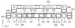
2 is a system configuration diagram showing a modification of Fig.
3 is a perspective view schematically showing an organic layer deposition apparatus according to an embodiment of the present invention.
4 is a schematic side cross-sectional view of the organic layer deposition apparatus of Fig.
5 is a schematic plan sectional view of the organic layer deposition apparatus of FIG.
6 is a plan view showing the arrangement of the substrate and the patterning slit sheet.
7 is a plan view showing the arrangement of the substrate and the patterning slit sheet according to another modification of the present invention.
8 is an image of the alignment pattern photographed by the camera assembly.
9 shows an alignment pattern and alignment of the alignment marks when the substrate and the patterning slit sheet are aligned along the first direction.
10 shows an alignment pattern and an alignment mark alignment when the substrate is moved along the X axis.
11 shows an alignment pattern and alignment of the alignment marks when the patterning slit sheet is rotated in the &thetas; direction.
12 shows an alignment pattern and alignment of the alignment marks when the substrate is rotated in the &thetas; direction.
13 is a perspective view schematically showing an organic layer deposition apparatus according to another embodiment of the present invention.
14 is a perspective view schematically showing an organic layer deposition apparatus according to another embodiment of the present invention.
15 is a perspective view schematically showing an organic layer deposition apparatus according to another embodiment of the present invention.
16 is a perspective view schematically showing an organic layer deposition apparatus according to another embodiment of the present invention.
17 is a schematic side cross-sectional view of the organic layer deposition apparatus of Fig.
18 is a schematic plan sectional view of the organic layer deposition apparatus of FIG.
19 is a perspective view schematically showing an organic layer deposition apparatus according to another embodiment of the present invention.
20 is a cross-sectional view of an organic light emitting display device that can be manufactured with an organic layer deposition apparatus according to the present invention.
이하, 첨부된 도면에 도시된 본 발명의 실시예를 참조하여 본 발명을 상세히 설명한다. 도면에서의 요소들의 형상 및 크기 등은 보다 명확한 설명을 위해 과장될 수 있으며, 도면상의 동일한 부호로 표시되는 요소는 동일한 요소이다.Hereinafter, the present invention will be described in detail with reference to embodiments of the present invention shown in the accompanying drawings. The shape and the size of the elements in the drawings may be exaggerated for clarity and the same elements are denoted by the same reference numerals in the drawings.
종래 파인 메탈 마스크를 이용하는 방법은 5G(1100mm X 1300mm) 이상의 마더 글래스(mother-glass)를 사용하는 대면적화에는 부적합하다는 한계가 있다. 즉, 대면적 마스크를 사용하면 자중에 의해 마스크의 휨 현상이 발생하는 데, 이 휨 현상에 의한 패턴의 왜곡이 발생할 수 있기 때문이다. 이는 패턴에 고정세를 요하는 현 경향과 배치되는 것이다.The conventional method using a fine metal mask has a limitation that it is unsuitable for the large-area use using a mother glass of 5G (1100 mm x 1300 mm) or more. That is, when a large-area mask is used, the mask is warped due to its own weight, and distortion of the pattern due to the warping phenomenon may occur. This is in line with the current tendency to require a fixed tax on the pattern.
도 1은 본 발명의 일 실시예에 관한 유기층 증착 장치를 포함한 유기층 증착 시스템 구성도이고, 도 2는 도 1의 변형예를 도시한 것이다.FIG. 1 is a structural view of an organic layer deposition system including an organic layer deposition apparatus according to an embodiment of the present invention, and FIG. 2 shows a modification of FIG.
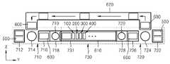
도 1을 참조하면, 본 발명의 일 실시예에 따른 유기층 증착 시스템은 로딩부(710), 증착부(730), 언로딩부(720), 제1순환부(610) 및 제2순환부(620)를 포함한다.Referring to FIG. 1, an organic layer deposition system according to an embodiment of the present invention includes a
로딩부(710)는 제1래크(712)와, 도입로봇(714)과, 도입실(716)과, 제1반전실(718)을 포함할 수 있다.The
제1래크(712)에는 증착이 이루어지기 전의 기판(500)이 다수 적재되어 있고, 도입로봇(714)은 상기 제1래크(712)로부터 기판(500)을 잡아 제2순환부(620)로부터 이송되어 온 정전척(600)에 기판(500)을 얹은 후, 기판(500)이 부착된 정전척(600)을 도입실(716)로 옮긴다.A plurality of
도입실(716)에 인접하게는 제1반전실(718)이 구비되며, 제1반전실(718)에 위치한 제1반전로봇(719)이 정전척(600)을 반전시켜 정전척(600)을 증착부(730)의 제1순환부(610)에 장착한다.A first inverting chamber 718 is provided adjacent to the introduction chamber 716 and a
도 1에서 볼 때, 도입로봇(714)은 정전척(600)의 상면에 기판(500)을 얹게 되고, 이 상태에서 정전척(600)은 도입실(716)로 이송되며, 제1반전로봇(719)이 정전척(600)을 반전시킴에 따라 증착부(730)에서는 기판(500)이 아래를 향하도록 위치하게 된다.1, the introduction robot 714 places the
언로딩부(720)의 구성은 위에서 설명한 로딩부(710)의 구성과 반대로 구성된다. 즉, 증착부(730)를 거친 기판(500) 및 정전척(600)을 제2 반전실(728)에서 제2 반전로봇(729)이 반전시켜 반출실(726)로 이송하고, 반출로봇(724)이 반출실(726)에서 기판(500) 및 정전척(600)을 꺼낸 다음 기판(500)을 정전척(600)에서 분리하여 제2래크(722)에 적재한다. 기판(500)과 분리된 정전척(600)은 제2순환부(620)를 통해 로딩부(710)로 회송된다.The configuration of the
그러나 본 발명은 반드시 이에 한정되는 것은 아니며, 기판(500)이 정전척(600)에 최초 고정될 때부터 정전척(600)의 하면에 기판(500)을 고정시켜 그대로 증착부(730)로 이송시킬 수도 있다. 이 경우, 예컨대 제1반전실(718) 및 제1 반전로봇(719)과 제2 반전실(728) 및 제2 반전로봇(729)은 필요 없게 된다.The
증착부(730)는 적어도 하나의 증착용 챔버를 구비한다. 도 1에 따른 본 발명의 바람직한 일 실시예에 따르면, 상기 증착부(730)는 제1챔버(731)를 구비하며, 이 제1챔버(731) 내에 복수의 유기층 증착 장치들(100)(200)(300)(400)이 배치된다. 도 1에 도시된 본 발명의 바람직한 일 실시예에 따르면, 상기 제1챔버(731) 내에 제1 유기층 증착 장치(100), 제2 유기층 증착 장치(200), 제3 유기층 증착 장치(300) 및 제4 유기층 증착 장치(400)의 네 개의 유기층 증착 장치들이 설치되어 있으나, 그 숫자는 증착 물질 및 증착 조건에 따라 가변 가능하다. 상기 제1챔버(731)는 증착이 진행되는 동안 진공으로 유지된다.The
또한, 도 2에 따른 본 발명의 다른 일 실시예에 따르면 상기 증착부(730)는 서로 연계된 제1챔버(731) 및 제2챔버(732)를 포함하고, 제1챔버(731)에는 제1, 2 유기층 증착 장치들(100)(200)이, 제2챔버(732)에는 제3, 4 유기층 증착 장치들(300)(400)이 배치될 수 있다. 이때, 챔버의 수가 추가될 수 있음은 물론이다.2, the
한편, 도 1에 따른 본 발명의 바람직한 일 실시예에 따르면, 상기 기판(500)이 고정된 정전척(600)은 제1순환부(610)에 의해 적어도 증착부(730)로, 바람직하게는 상기 로딩부(710), 증착부(730) 및 언로딩부(720)로 순차 이동되고, 상기 언로딩부(720)에서 기판(500)과 분리된 정전척(600)은 제2순환부(620)에 의해 상기 로딩부(710)로 환송된다.1, the
상기 제1순환부(610)는 상기 증착부(730)를 통과할 때에 상기 제1챔버(731)를 관통하도록 구비되고, 상기 제2순환부(620)는 정전 척이 이송되도록 구비된다.The
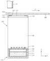
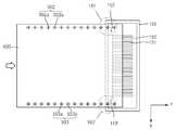
도 3은 본 발명의 유기층 증착 장치의 일 실시예를 개략적으로 도시한 사시도이고, 도 4는 도 3의 유기층 증착 장치의 개략적인 측면도이고, 도 5은 도 3의 유기층 증착 장치의 개략적인 평면도이다.FIG. 3 is a perspective view schematically showing one embodiment of the organic layer deposition apparatus of the present invention, FIG. 4 is a schematic side view of the organic layer deposition apparatus of FIG. 3, and FIG. 5 is a schematic plan view of the organic layer deposition apparatus of FIG. 3 .
도 3 내지 도 5를 참조하면, 본 발명의 일 실시예에 관한 유기층 증착 장치(100)는 증착원(110), 증착원 노즐부(120), 패터닝 슬릿 시트(150), 제1, 2 카메라 어셈블리(161, 162) 및 제어부(170)를 포함한다.3 to 5, an organic
상세히, 증착원(110)에서 방출된 증착 물질(115)이 증착원 노즐부(120) 및 패터닝 슬릿 시트(150)를 통과하여 기판(500)에 원하는 패턴으로 증착되게 하려면, 기본적으로 제1 챔버(731) 내부는 FMM 증착 방법과 동일한 고진공 상태를 유지해야 한다. 또한 패터닝 슬릿 시트(150)의 온도가 증착원(110) 온도보다 충분히 낮아야(약 100°이하) 한다. 왜냐하면, 패터닝 슬릿 시트(150)의 온도가 충분히 낮아야만 온도에 의한 패터닝 슬릿 시트(150)의 열팽창 문제를 최소화할 수 있기 때문이다.More specifically, in order for the
이러한 제1 챔버(731) 내에는 피 증착체인 기판(500)이 배치된다. 상기 기판(500)은 평판 표시장치용 기판이 될 수 있는데, 다수의 평판 표시장치를 형성할 수 있는 마더 글라스(mother glass)와 같은 대면적 기판이 적용될 수 있다.In this
여기서, 본 발명의 일 실시예에서는, 기판(500)이 유기층 증착 장치(100)에 대하여 상대적으로 이동하면서 증착이 진행되는 것을 일 특징으로 한다.Here, in one embodiment of the present invention, the deposition is progressed while the
상세히, 기존 FMM 증착 방법에서는 FMM 크기가 기판 크기와 동일하게 형성되어야 한다. 따라서, 기판 사이즈가 증가할수록 FMM도 대형화되어야 하며, 이로 인해 FMM 제작이 용이하지 않고, FMM을 인장하여 정밀한 패턴으로 얼라인(align) 하기도 용이하지 않다는 문제점이 존재하였다.Specifically, in the conventional FMM deposition method, the FMM size must be formed equal to the substrate size. Therefore, as the substrate size increases, the FMM must be made larger, which makes it difficult to fabricate the FMM, and it is not easy to align the FMM with a precise pattern by pulling the FMM.
이와 같은 문제점을 해결하기 위하여, 본 발명의 일 실시예에 관한 유기층 증착 장치(100)는, 유기층 증착 장치(100)와 기판(500)이 서로 상대적으로 이동하면서 증착이 이루어지는 것을 일 특징으로 한다. 다시 말하면, 유기층 증착 장치(100)와 마주보도록 배치된 기판(500)이 Y축 방향을 따라 이동하면서 연속적으로 증착을 수행하게 된다. 즉, 기판(500)이 도 6의 화살표 P 방향(제1 방향)으로 이동하면서 스캐닝(scanning) 방식으로 증착이 수행되는 것이다.In order to solve such a problem, the organic
본 발명의 유기층 증착 장치(100)에서는 종래의 FMM에 비하여 훨씬 작게 패터닝 슬릿 시트(150)를 만들 수 있다. 즉, 본 발명의 유기층 증착 장치(100)의 경우, 기판(500)이 Y축 방향을 따라 이동하면서 연속적으로, 즉 스캐닝(scanning) 방식으로 증착을 수행하기 때문에, 패터닝 슬릿 시트(150)의 X축 방향 및 Y축 방향의 길이는 기판(500)의 길이보다 훨씬 작게 형성될 수 있는 것이다. 이와 같이, 종래의 FMM에 비하여 훨씬 작게 패터닝 슬릿 시트(150)를 만들 수 있기 때문에, 본 발명의 패터닝 슬릿 시트(150)는 그 제조가 용이하다. 즉, 패터닝 슬릿 시트(150)의 에칭 작업이나, 그 이후의 정밀 인장 및 용접 작업, 이동 및 세정 작업 등 모든 공정에서, 작은 크기의 패터닝 슬릿 시트(150)가 FMM 증착 방법에 비해 유리하다. 또한, 이는 디스플레이 장치가 대형화될수록 더욱 유리하게 된다.The
한편, 챔버 내에서 상기 기판(500)과 대향하는 측에는, 증착 물질(115)이 수납 및 가열되는 증착원(110)이 배치된다. 상기 증착원(110) 내에 수납되어 있는 증착 물질(115)이 기화됨에 따라 기판(500)에 증착이 이루어진다.On the other hand, on the side facing the
상세히, 증착원(110)은 그 내부에 증착 물질(115)이 채워지는 도가니(112)와, 도가니(112)를 가열시켜 도가니(112) 내부에 채워진 증착 물질(115)을 도가니(112)의 일 측, 상세하게는 증착원 노즐부(120) 측으로 증발시키기 위한 냉각 블록(111)을 포함한다. 냉각 블록(111)은 도가니(112)로부터의 열이 외부, 즉, 제1챔버 내부로 발산되는 것을 최대한 억제하기 위한 것으로, 이 냉각 블록(111)에는 도가니(112)를 가열시키는 히터(미도시)가 포함되어 있다.In detail, the
증착원(110)의 일측, 상세하게는 증착원(110)에서 기판(500)을 향하는 측에는 증착원 노즐부(120)가 배치된다. 그리고, 증착원 노즐부(120)에는, Y축 방향 즉 기판(500)의 스캔 방향을 따라서 복수 개의 증착원 노즐(121)들이 형성된다. 여기서, 상기 복수 개의 증착원 노즐(121)들은 등 간격으로 형성될 수 있다. 증착원(110) 내에서 기화된 증착 물질(115)은 이와 같은 증착원 노즐부(120)를 통과하여 피 증착체인 기판(500) 쪽으로 향하게 되는 것이다. 이와 같이, 증착원 노즐부(120) 상에 Y축 방향 즉 기판(500)의 스캔 방향을 따라서 복수 개의 증착원 노즐(121)들이 형성할 경우, 패터닝 슬릿 시트(150)의 각각의 패터닝 슬릿(151)들을 통과하는 증착 물질에 의해 형성되는 패턴의 크기는 증착원 노즐(121) 하나의 크기에만 영향을 받으므로(즉, X축 방향으로는 증착원 노즐(121)이 하나만 존재하는 것에 다름 아니므로), 음영(shadow)이 발생하지 않게 된다. 또한, 다수 개의 증착원 노즐(121)들이 스캔 방향으로 존재하므로, 개별 증착원 노즐 간 플럭스(flux) 차이가 발생하여도 그 차이가 상쇄되어 증착 균일도가 일정하게 유지되는 효과를 얻을 수 있다.The evaporation
한편, 증착원(110)과 기판(500) 사이에는 패터닝 슬릿 시트(150) 및 프레임(155)이 더 구비된다. 프레임(155)은 대략 창문 틀과 같은 형태로 형성되며, 그 내측에 패터닝 슬릿 시트(150)가 결합된다. 그리고, 패터닝 슬릿 시트(150)에는 X축 방향을 따라서 복수 개의 패터닝 슬릿(151)들이 형성된다. 증착원(110) 내에서 기화된 증착 물질(115)은 증착원 노즐부(120) 및 패터닝 슬릿 시트(150)를 통과하여 피 증착체인 기판(500) 쪽으로 향하게 되는 것이다. 이때, 상기 패터닝 슬릿 시트(150)는 종래의 파인 메탈 마스크(FMM) 특히 스트라이프 타입(stripe type)의 마스크의 제조 방법과 동일한 방법인 에칭을 통해 제작될 수 있다. 이때, 증착원 노즐(121)들의 총 개수보다 패터닝 슬릿(151)들의 총 개수가 더 많게 형성될 수 있다.A
한편, 상술한 증착원(110)(및 이와 결합된 증착원 노즐부(120))과 패터닝 슬릿 시트(150)는 서로 일정 정도 이격되도록 형성될 수 있으며, 증착원(110)(및 이와 결합된 증착원 노즐부(120))과 패터닝 슬릿 시트(150)는 제1 연결 부재(135)에 의하여 서로 연결될 수 있다. 즉, 증착원(110), 증착원 노즐부(120) 및 패터닝 슬릿 시트(150)가 제1연결 부재(135)에 의해 연결되어 서로 일체로 형성될 수 있는 것이다. 여기서 제1연결 부재(135)들은 증착원 노즐(121)을 통해 배출되는 증착 물질이 분산되지 않도록 증착 물질의 이동 경로를 가이드 할 수 있다. 도면에는 제1 연결 부재(135)가 증착원(110), 증착원 노즐부(120) 및 패터닝 슬릿 시트(150)의 좌우 방향으로만 형성되어 증착 물질의 X축 방향만을 가이드 하는 것으로 도시되어 있으나, 이는 도시의 편의를 위한 것으로, 본 발명의 사상은 이에 제한되지 아니하며, 제1 연결 부재(135)가 박스 형태의 밀폐형으로 형성되어 증착 물질의 X축 방향 및 Y축 방향 이동을 동시에 가이드 할 수도 있다.The
상술한 바와 같이, 본 발명의 일 실시예에 관한 유기층 증착 장치(100)는 기판(500)에 대하여 상대적으로 이동하면서 증착을 수행하며, 이와 같이 유기층 증착 장치(100)가 기판(500)에 대하여 상대적으로 이동하기 위해서 패터닝 슬릿 시트(150)는 기판(500)으로부터 일정 정도 이격되도록 형성된다.As described above, the organic
상세히, 종래의 FMM 증착 방법에서는 기판에 음영(shadow)이 생기지 않도록 하기 위하여 기판에 마스크를 밀착시켜서 증착 공정을 진행하였다. 그러나, 이와 같이 기판에 마스크를 밀착시킬 경우, 기판과 마스크 간의 접촉에 의한 불량 문제가 발생한다는 문제점이 존재하였다. 또한, 마스크를 기판에 대하여 이동시킬 수 없기 때문에, 마스크가 기판과 동일한 크기로 형성되어야 한다. 따라서, 디스플레이 장치가 대형화됨에 따라 마스크의 크기도 커져야 하는데, 이와 같은 대형 마스크를 형성하는 것이 용이하지 아니하다는 문제점이 존재하였다.In detail, in the conventional FMM deposition method, a mask is closely adhered to a substrate to prevent a shadow from being formed on the substrate, and a deposition process is performed. However, when the mask is brought into close contact with the substrate in this manner, there is a problem that a problem of defective due to contact between the substrate and the mask occurs. Further, since the mask can not be moved relative to the substrate, the mask must be formed to have the same size as the substrate. Therefore, as the size of the display device is increased, the size of the mask must be increased. Thus, there is a problem that it is not easy to form such a large mask.
이와 같은 문제점을 해결하기 위하여, 본 발명의 일 실시예에 관한 유기층 증착 장치(100)에서는 패터닝 슬릿 시트(150)가 피 증착체인 기판(500)과 소정 간격을 두고 이격되도록 배치되도록 한다.In order to solve such a problem, in the organic
이와 같은 본 발명에 의해서 마스크를 기판보다 작게 형성한 후, 마스크를 기판에 대하여 이동시키면서 증착을 수행할 수 있게 됨으로써, 마스크 제작이 용이해지는 효과를 얻을 수 있다. 또한, 기판과 마스크 간의 접촉에 의한 불량을 방지하는 효과를 얻을 수 있다. 또한, 공정에서 기판과 마스크를 밀착시키는 시간이 불필요해지기 때문에, 제조 속도가 향상되는 효과를 얻을 수 있다.According to the present invention, after the mask is formed smaller than the substrate, the deposition can be performed while moving the mask relative to the substrate, so that it is possible to obtain an effect of facilitating the production of the mask. In addition, it is possible to obtain an effect of preventing defects due to contact between the substrate and the mask. Further, since the time required for the substrate and the mask to adhere to each other in the process becomes unnecessary, an effect of improving the manufacturing speed can be obtained.
본 발명의 일 실시예에 관한 유기층 증착 장치(100)는 기판(500)과 패터닝 슬릿 시트(150)의 얼라인을 위해 제1, 2 얼라인 패턴(502, 503), 제1, 2 얼라인 마크(152, 153), 제1, 2 카메라 어셈블리(161, 162), 및 제어부(170)를 구비할 수 있다.The organic
제1, 2 얼라인 패턴(502, 503)은 기판(500)의 이송 방향(P)을 따라 기판(500) 상에 형성된다. 제1, 2 얼라인 패턴(502, 503)은 서로 이격되어 기판(500)의 양단부에 형성될 수 있다. 제1 얼라인 패턴(502)은 기판(500)의 이송 방향(P)을 따라 배열된 복수 개의 제1 마크(502a)로 이루어지며, 제2 얼라인 패턴(503)은 상기 이송 방향(P)을 따라 배열된 복수 개의 제2 마크(503a)로 이루어질 수 있다. 제1, 2 마크(502a, 503a)는 열십자(十) 형상일 수 있다. 제1 마크(502a)들 사이의 간격을 일정하며, 제2 마크(503a)들 사이의 간격 또한 일정할 수 있다. 또한, 제1 마크(502a)들 사이의 간격과 제2 마크(503a)들 사이의 간격은 동일할 수 있다.First and
제1, 2 얼라인 마크(152, 153)는 패터닝 슬릿 시트(150)의 양단부에 형성될 수 있다. 제1, 2 얼라인 마크(152, 153)는 상기 이송 방향(P)에 수직한 방향(제2 방향)로 서로 이격되어 형성될 수 있다. 제1, 2 얼라인 마크(152, 153)는 원형일 수 있다. 본 발명은 이에 한정되는 것은 아니며, 제1, 2 얼라인 마크(152, 153)는 다각형일 수 있다. 예를 들어, 제1, 2 얼라인 마크(152, 153)가 직각 삼각형일 경우, 빗변이 패터닝 슬릿(151)을 향하도록 형성될 수 있다.The first and second alignment marks 152 and 153 may be formed at both ends of the
기판(500)과 패터닝 슬릿 시트(150)가 올바르게 얼라인된 경우 제1, 2 얼라인 마크(152, 153)는 제1 얼라인 패턴(502)과 제2 얼라인 패턴(503) 사이에 위치한다. 이에 관하여는 후술한다.The first and second alignment marks 152 and 153 are positioned between the
제1 카메라 어셈블리(161)는 제1 얼라인 마크(152)에 대응되도록 기판(500) 상에 배치되며, 제2 카메라 어셈블리(162)는 제2 얼라인 마크(153)에 대응되도록 기판(500) 상에 배치될 수 있다. 제1 카메라 어셈블리(161)는 기판(500) 상에서 제1 얼라인 패턴(502)과 제1 얼라인 마크(152)를 촬영하며, 제2 카메라 어셈블리(162)는 기판(500) 상에서 제2 얼라인 패턴(503)과 제2 얼라인 마크(153)를 촬영할 수 있다. 기판(500)은 투명하므로 제1, 2 카메라 어셈블리(161, 162)가 기판(500)을 통해 제1, 2 얼라인 마크(152, 153)을 촬영하는 것이 가능하다. 제1, 2 카메라 어셈블리(161, 162)이 배열된 방향은 상기 이송 방향(P)에 수직한 방향(제2 방향)일 수 있다.The
제어부(170)은 제1, 2 카메라 어셈블리(161, 162)에 의해 촬영된 정보를 분석하여 기판(500)과 패터닝 슬릿 시트(150) 사이의 얼라인 정도를 판별하며, 상기 얼라인 정도에 따라 기판(500) 또는 패터닝 슬릿 시트(150)를 이동시킬 수 있는 구동부(미도시)를 제어할 수 있다.The
도 6 내지 12를 참조하여 기판(500)과 패터닝 슬릿 시트(150) 사이의 얼라인을 설명한다.The alignment between the
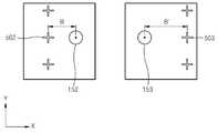
도 6은 제1, 2 카메라 어셈블리(161, 162)에서 바라본 기판(500)과 패터닝 슬릿 시트(150)의 평면도이다.6 is a plan view of the
도 6을 참조하면, 기판(500)은 Y축 방향으로 이송된다. 제1, 2 얼라인 패턴(502, 503)은 기판(500)의 이송 방향인 Y 방향과 평행하게 형성되며, 제1 얼라인 패턴(502)와 제2 얼라인 패턴(503)은 Y 방향에 수직한 방향(제2 방향)으로 서로 이격되어 기판(500)의 양단부에 배치될 수 있다.Referring to FIG. 6, the
패터닝 슬릿 시트(150) 상에 형성된 제1, 2 얼라인 마크(152, 153)는 상기 제2 방향으로 서로 이격되어 있으며, 제1 얼라인 패턴(502)과 제2 얼라인 패턴(503) 사이에 배치될 수 있다.The first and second alignment marks 152 and 153 formed on the
도 7은 본 발명의 다른 변형예에 따른 기판과 패터닝 슬릿 시트의 배열을 나타내는 평면도이다. 도 7을 참조하면, 기판(500')은 삼각형 형상을 갖는 제1, 2 얼라인 패턴(602, 603)을 가질 수 있다. 제1, 2 얼라인 패턴(602, 603)은 직각 삼각형 형성을 갖는 얼라인 마크가 연속적으로 배열되어 톱니 형태를 이룰 수 있다. 본 발명은 이에 한정되는 것은 아니며, 제1, 2 얼라인 패턴(602, 603)은 다각형의 얼라인 마크가 연속적으로 배열된 형태를 가질 수 있다.7 is a plan view showing an arrangement of a substrate and a patterning slit sheet according to another modification of the present invention. Referring to FIG. 7, the substrate 500 'may have first and
도 8은 카메라 어셈블리에 의해 촬영된 얼라인 패턴의 영상이다. 도 8을 참조하면, 왼쪽 그림은 제1 카메라 어셈블리(161)가 촬영한 제1 얼라인 패턴(502)의 영상이며, 오른쪽 그림은 제2 카메라 어셈블리(162)가 촬영한 제2 얼라인 패턴(503)의 영상이다. 제1, 2 카메라 어셈블리(161, 162)의 촬영 속도와 기판(500)의 이동 속도는 동기화되며, 이에 따라, 제1, 2 카메라 어셈블리(161, 162)는 동일한 영상의 제1, 2 얼라인 패턴(502, 503)을 촬영할 수 있다. 보다 상세하게는, 제1, 2 카메라 어셈블리(161, 162) 각각은 일정한 시간 간격으로 이동하는 기판(500)을 촬영할 수 있다. 제1, 2 카메라 어셈블리(161, 162)의 촬영 시간 동안에 일정한 속도로 기판(500)이 이동하므로 제1, 2 카메라 어셈블리(161, 162)는 도 8에 도시된 바와 같이 동일한 영상의 제1, 2 얼라인 패턴(502, 503)을 촬영할 수 있다.8 is an image of the alignment pattern photographed by the camera assembly. 8, the left image is the image of the
도 9는 기판(500)과 패터닝 슬릿 시트(150)이 올바르게 얼라인된 상태의 제1, 2 얼라인 패턴(502, 503)과 제1, 2 얼라인 마크(152, 153)를 도시한다.9 shows the first and
도 9를 참조하면, 제1 카메라 어셈블리(161)는 제1 얼라인 마크(152) 상에 배치되고, 제2 카메라 어셈블리(162)는 제2 얼라인 마크(153) 상에 배치되며, 제1 카메라 어셈블리(161)는 제1 얼라인 패턴(502)와 제1 얼라인 마크(152)를 도 9의 왼쪽 그림과 같이 촬영하고, 제2 카메라 어셈블리(162)는 제2 얼라인 패턴(503)와 제2 얼라인 마크(153)를 도 9의 오른쪽 그림과 같이 촬영할 수 있다. 기판(500)과 패터닝 슬릿 시트(150)이 올바르게 얼라인된 상태인 경우, 제1 얼라인 패턴(502)과 제1 얼라인 마크(152) 사이의 간격(A)과, 제2 얼라인 패턴(503)과 제2 얼라인 마크(153) 사이의 간격(A')이 동일하다.9, the
도 10은 기판이 X축으로 이동된 경우의 얼라인 패턴과 얼라인 마크의 배열을 나타낸다.10 shows an alignment pattern and an alignment mark alignment when the substrate is moved along the X axis.
도 10을 참조하면, 기판(500)이 X축 방향으로 이동한 경우, 제1 얼라인 패턴(502)과 제1 얼라인 마크(152) 사이의 간격(B)이 제2 얼라인 패턴(503)과 제2 얼라인 마크(153) 사이의 간격(B')보다 작게 된다.10, when the
기판(500)이 X축 방향으로 이동한 경우, 제어부(170)은 기판(500)을 X축 방향으로 (B'-B)/2 거리 만큼 이동시키도록 구동부(미도시)를 제어한다.When the
도 11은 패터닝 슬릿 시트가 θ방향으로 틀어진 경우의 얼라인 패턴과 얼라인 마크의 배열을 나타낸다. 패터닝 슬릿 시트(150)이 θ방향으로 틀어진 경우는 패터닝 슬릿 시트(150)가 Z축을 중심으로 반시계 방향(θ방향) 또는 시계 방향(-θ방향)으로 이동된 경우를 의미한다.11 shows an alignment pattern and alignment of the alignment marks when the patterning slit sheet is rotated in the &thetas; direction. When the
도 11을 참조하면, 패터닝 슬릿 시트(150)가 θ방향(반시계 방향)으로 틀어진 경우, 제2 카메라 어셈블리(162)에 의해 촬영된 제2 얼라인 마크(153)는 제1 카메라 어셈블리(161)에 의해 촬영된 제1 얼라인 마크(152)에 비해 Y축 방향으로 앞서게 된다. 즉, 제1 얼라인 마크(152)를 기준으로 보면, 제2 얼라인 마크(153)의 Y축 좌표는 제1 얼라인 마크(152)의 Y축 좌표보다 h1 만큼 크게 된다. 패터닝 슬릿 시트(150)가 틀어진 정도는 제1 얼라인 마크(152)와 제2 얼라인 마크(153) 사이의 거리(D1), 그리고 제1 얼라인 마크(152)와 제2 얼라인 마크(153)의 Y축 좌표에서의 차이(h1)로 구할 수 있다. 상세하게는 패터닝 슬릿 시트(150)가 틀어진 각도(θ1)는 Arctan(h1/D1)에 해당한다. 이와 같은 경우 제어부(170)는 패터닝 슬릿 시트(150)를 -θ1방향(시계 방향)으로 Arctan(h1/D1) 각도만큼 이동시키도록 구동부(미도시)를 제어한다.11, when the
도 12는 기판이 θ방향으로 틀어진 경우의 얼라인 패턴과 얼라인 마크의 배열을 나타낸다. 기판(500)이 θ방향으로 틀어진 경우는 기판(500)이 Z축을 중심으로 반시계 방향(θ방향) 또는 시계 방향(-θ방향)으로 이동된 경우를 의미한다.12 shows an alignment pattern and alignment of the alignment marks when the substrate is rotated in the &thetas; direction. When the
도 12를 참조하면, 기판(500)이 θ방향(반시계 방향)으로 틀어진 경우, 제2 카메라 어셈블리(162)에 의해 촬영된 제2 얼라인 패턴(503)은 제1 카메라 어셈블리(161)에 의해 촬영된 제1 얼라인 패턴(502)에 비해 Y축 방향으로 앞서게 된다. 즉, 제1 얼라인 패턴(502)을 기준으로 보면, 제2 얼라인 패턴(503)의 Y축 좌표는 제1 얼라인 패턴(502)의 Y축 좌표보다 h2 만큼 크게 된다. 기판(500)이 틀어진 정도는 제1 얼라인 패턴(502)과 제2 얼라인 패턴(503) 사이의 거리(D2), 그리고 제1 얼라인 패턴(502)와 제2 얼라인 패턴(503)의 Y축 좌표에서의 차이(h2)로 구할 수 있다. 상세하게는 기판(500)이 틀어진 각도(θ2)는 Arctan(h2/D2)에 해당한다. 이와 같은 경우 제어부(170)는 기판(500)을 -θ방향(시계 방향)으로 Arctan(h2/D2) 각도만큼 이동시키도록 구동부(미도시)를 제어한다.12, when the
이와 같이, 본 발명의 일 실시예에 따른 유기층 증착 장치(100)는 기판(500)이 이송 방향에 수직인 방향(제2 방향)으로 이동된 경우뿐만 아니라 이송 방향(제1 방향)에 대해 틀어진 경우에도 기판(500)과 얼라인 패터닝 슬릿 시트(150)의 얼라인을 제어할 수 있다.As described above, the organic
도 13은 본 발명의 다른 실시예에 관한 유기층 증착 장치를 개략적으로 도시한 사시도이다. 도 13을 참조하면, 본 발명의 다른 실시예에 관한 유기층 증착 장치(100a)는 제3 얼라인 마크(152'), 제4 얼라인 마크(153'), 제3 카메라 어셈블리(161'), 및 제4 카메라 어셈블리(162')를 더 구비한다는 점에서 도 3에 도시된 유기층 증착 장치(100)와 차이가 있다.13 is a perspective view schematically showing an organic layer deposition apparatus according to another embodiment of the present invention. Referring to FIG. 13, the organic
상세하게는, 도 13에 도시된 유기층 증착 장치(100a)의 패터닝 슬릿 시트(150')는 제3 얼라인 마크(152')와 제4 얼라인 마크(153')를 더 구비할 수 있다. 제3 얼라인 마크(152')는 제1 얼라인 마크(152)에서 제1 방향(Y축 방향)을 따라 이격되도록 배치되며, 제4 얼라인 마크(153')는 제2 얼라인 마크(153)에서 제1 방향(Y축 방향)을 따라 이격되도록 배치될 수 있다. 제1 얼라인 마크(152)와 제3 얼라인 마크(152') 사이의 간격은 제2 얼라인 마크(153)과 제4 얼라인 마크(153') 사이의 간격과 동일할 수 있다. 또한, 제1 얼라인 마크(152)와 제2 얼라인 마크(153)은 제2 방향(X축 방향)으로 서로 이격되어 있으며, 제3 얼라인 마크(152')와 제4 얼라인 마크(153') 역시 제2 방향(X축 방향)으로 서로 이격되어 있다. 제1 얼라인 마크(152)와 제2 얼라인 마크(153) 사이의 간격은 제3 얼라인 마크(152')와 제4 얼라인 마크(153') 사이의 간격과 동일할 수 있다.In detail, the patterning slit sheet 150 'of the organic
도 13에 도시된 유기층 증착 장치(100a)는 제3 카메라 어셈블리(161')와 제4 카메라 어셈블리(162')를 더 구비할 수 있다. 제1, 2, 3, 4 카메라 어셈블리(161, 162, 161', 162') 각각은 제1, 2, 3, 4 얼라인 마크(152, 153, 152', 153')에 대응되도록 기판(500) 상에 배치될 수 있다. 제3 카메라 어셈블리(161')와 제4 카메라 어셈블리(162')의 촬영 속도는 기판(500)의 이동 속도와 동기화될 수 있다. 따라서, 제3 카메라 어셈블리(161')에 의해 촬영되는 영상들은 동일한 모양과 크기를 갖는 제1 얼라인 패턴(502)을 가지며, 제4 카메라 어셈블리(162')에 의해 촬영되는 영상들은 동일한 모양과 크기를 갖는 제2 얼라인 패턴(503)을 가질 수 있다.The organic
도 14은 본 발명의 유기층 증착 장치의 다른 실시예를 나타내는 도면이다. 도면을 참조하면, 본 발명의 다른 실시예에 따른 유기층 증착 장치는 증착원(110'), 증착원 노즐부(120), 및 패터닝 슬릿 시트(150)를 포함한다. 여기서, 증착원(110')은 그 내부에 증착 물질(115)이 채워지는 도가니(112)와, 도가니(112)를 가열시켜 도가니(112) 내부에 채워진 증착 물질(115)을 증착원 노즐부(120) 측으로 증발시키기 위한 냉각 블록(111)을 포함한다. 한편, 증착원(110')의 일 측에는 증착원 노즐부(120)가 배치되고, 증착원 노즐부(120)에는 Y축 방향을 따라서 복수 개의 증착원 노즐(121)들이 형성된다. 한편, 증착원(110')과 기판(500) 사이에는 패터닝 슬릿 시트(150) 및 프레임(155)이 더 구비되고, 패터닝 슬릿 시트(150)에는 X축 방향을 따라서 복수 개의 패터닝 슬릿(151a)들이 형성된다. 그리고 증착원(110') 및 증착원 노즐부(120)와 패터닝 슬릿 시트(150)는 제2연결 부재(133)에 의해서 결합된다.14 is a view showing another embodiment of the organic layer deposition apparatus of the present invention. Referring to the drawings, an organic layer deposition apparatus according to another embodiment of the present invention includes an evaporation source 110 ', an evaporation
본 실시예에서는, 증착원 노즐부(120)에 형성된 복수 개의 증착원 노즐(121')들이 소정 각도 틸트(tilt)되어 배치된다는 점에서 도 4에 도시된 유기층 증착 장치와 구별된다. 상세히, 증착원 노즐(121')은 두 열의 증착원 노즐(121'a)(121'b)들로 이루어질 수 있으며, 상기 두 열의 증착원 노즐(121'a)(121'b)들은 서로 교번하여 배치된다. 이때, 증착원 노즐(121'a)(121'b)들은 XZ 평면상에서 소정 각도 기울어지도록 틸트(tilt)되어 형성될 수 있다.This embodiment is distinguished from the organic layer deposition apparatus shown in FIG. 4 in that a plurality of evaporation source nozzles 121 'formed in the evaporation
본 실시예에서는 증착원 노즐(121'a)(121'b)들이 소정 각도 틸트되어 배치되도록 한다. 여기서, 제1 열의 증착원 노즐(121'a)들은 제2 열의 증착원 노즐(121'b)들을 바라보도록 틸트되고, 제2 열의 증착원 노즐(121'b)들은 제1 열의 증착원 노즐(121'a)들을 바라보도록 틸트될 수 있다. 다시 말하면, 왼쪽 열에 배치된 증착원 노즐(121'a)들은 패터닝 슬릿 시트(150)의 오른쪽 단부를 바라보도록 배치되고, 오른쪽 열에 배치된 증착원 노즐(121'b)들은 패터닝 슬릿 시트(150)의 왼쪽 단부를 바라보도록 배치될 수 있는 것이다.In this embodiment, the evaporation source nozzles 121'a and 121'b are arranged to be tilted at a predetermined angle. Here, the evaporation source nozzles 121'a of the first row are tilted so as to face the evaporation source nozzles 121'b of the second row, the evaporation source nozzles 121'b of the second row are tilted so as to face the evaporation source nozzles 121'b of the first row 121'a. In other words, the evaporation source nozzles 121'a disposed in the left column are disposed to face the right end of the
이와 같은 구성에 의하여, 기판의 중앙과 끝 부분에서의 성막 두께 차이가 감소하게 되어 전체적인 증착 물질의 두께가 균일하도록 증착량을 제어할 수 있으며, 나아가서는 재료 이용 효율이 증가하는 효과를 얻을 수 있다.According to this structure, the difference in the film thickness between the center and the end of the substrate is reduced, and the deposition amount can be controlled so that the thickness of the entire deposition material can be controlled uniformly. In addition, .
도 15는 본 발명의 유기층 증착 장치의 또 다른 실시예를 나타내는 도면이다. 도면을 참조하면, 본 발명의 또 다른 실시예에 따른 유기층 증착 장치는 도 4 내지 도 6에서 설명한 유기층 증착 장치가 복수 개 구비되는 것을 일 특징으로 한다. 다시 말하면, 본 발명의 일 실시예에 관한 유기층 증착 장치는, 적색 발광층(R) 재료, 녹색 발광층(G) 재료, 청색 발광층(B) 재료가 한꺼번에 방사되는 멀티 증착원(multi source)을 구비할 수 있는 것이다.15 is a view showing still another embodiment of the organic layer deposition apparatus of the present invention. Referring to the drawings, an organic layer deposition apparatus according to another embodiment of the present invention includes a plurality of organic layer deposition apparatuses described with reference to FIGS. In other words, the organic layer deposition apparatus according to one embodiment of the present invention includes a multi source in which a red light emitting layer (R) material, a green light emitting layer (G) material, and a blue light emitting layer (B) You can.
상세히, 본 실시예는 제1 유기층 증착 장치(100), 제2 유기층 증착 장치(200) 및 제3 유기층 증착 장치(300)를 포함한다. 이와 같은 제1 유기층 증착 장치(100), 제2 유기층 증착 장치(200) 및 제3 유기층 증착 장치(300) 각각의 구성은 도 3 내지 도 5에서 설명한 유기층 증착 장치와 동일하므로 여기서는 그 상세한 설명은 생략하도록 한다.Specifically, this embodiment includes a first organic
여기서, 제1 유기층 증착 장치(100), 제2 유기층 증착 장치(200) 및 제3 유기층 증착 장치(300)의 증착원에는 서로 다른 증착 물질들이 구비될 수 있다. 예를 들어, 제1 유기층 증착 장치(100)에는 적색 발광층(R)의 재료가 되는 증착 물질이 구비되고, 제2 유기층 증착 장치(200)에는 녹색 발광층(G)의 재료가 되는 증착 물질이 구비되고, 제3 유기층 증착 장치(300)에는 청색 발광층(B)의 재료가 되는 증착 물질이 구비될 수 있다.Here, the evaporation sources of the first organic
즉, 종래의 유기 발광 디스플레이 장치의 제조 방법에서는, 각 색상 별로 별도의 챔버와 마스크를 구비하는 것이 일반적이었으나, 본 발명의 일 실시예에 관한 유기층 증착 장치를 이용하면, 하나의 멀티 소스로 적색 발광층(R), 녹색 발광층(G) 및 청색 발광층(B)을 한꺼번에 증착할 수 있는 것이다. 따라서, 유기 발광 디스플레이 장치의 생산 시간이 획기적으로 감소하는 동시에, 구비되어야 하는 챔버 수가 감소함으로써, 설비 비용 또한 현저하게 절감되는 효과를 얻을 수 있다.In other words, in the conventional method of manufacturing an organic light emitting display device, it is common to provide a separate chamber and mask for each color. However, when the organic layer deposition apparatus according to an embodiment of the present invention is used, (R), the green light-emitting layer (G), and the blue light-emitting layer (B) can be deposited all at once. Therefore, the production time of the organic light emitting display device is drastically reduced, and the number of chambers to be provided is reduced, so that the facility cost can be remarkably reduced.
이 경우, 도면에는 자세히 도시되지 않았지만, 제1 유기층 증착 장치(100), 제2 유기층 증착 장치(200) 및 제3 유기층 증착 장치(300)의 패터닝 슬릿 시트들은 서로 일정 정도 오프셋(offset) 되어 배치됨으로써, 그 증착 영역이 중첩되지 아니하도록 할 수 있다. 다시 말하면, 제1 유기층 증착 장치(100)가 적색 발광층(R)의 증착을 담당하고, 제2 유기층 증착 장치(200)가 녹색 발광층(G)의 증착을 담당하고, 제3 유기층 증착 장치(300)가 청색 발광층(B)의 증착을 담당할 경우, 제1 유기층 증착 장치(100)의 패터닝 슬릿(151a)과 제2 유기층 증착 장치(200)의 패터닝 슬릿(251)과 제3 유기층 증착 장치(300)의 패터닝 슬릿(351)이 서로 동일 선상에 위치하지 아니하도록 배치됨으로써, 기판상의 서로 다른 영역에 각각 적색 발광층(R), 녹색 발광층(G), 청색 발광층(B)이 형성되도록 할 수 있다.In this case, the patterning slit sheets of the first organic
여기서, 적색 발광층(R)의 재료가 되는 증착 물질과, 녹색 발광층(G)의 재료가 되는 증착 물질과, 청색 발광층(B)의 재료가 되는 증착 물질은 서로 기화되는 온도가 상이할 수 있으므로, 상기 제1 유기층 증착 장치(100)의 증착원(110)의 온도와 상기 제2 유기층 증착 장치(200)의 증착원의 온도와 상기 제3 유기층 증착 장치(300)의 증착원의 온도가 서로 다르도록 설정되는 것도 가능하다 할 것이다.Here, the deposition material to be the material of the red luminescent layer (R), the deposition material to be the material of the green luminescent layer (G), and the deposition material to be the material of the blue luminescent layer (B) The temperature of the
한편, 도면에는 유기층 증착 장치가 세 개 구비되는 것으로 도시되어 있으나, 본 발명의 사상은 이에 제한되지 아니한다. 즉, 본 발명의 일 실시예에 관한 유기층 증착 장치는 유기층 증착 장치를 다수 개 구비할 수 있으며, 상기 다수 개의 유기층 증착 장치 각각에 서로 다른 물질들을 구비할 수 있다. 예를 들어, 유기층 증착 장치를 다섯 개 구비하여, 각각의 유기층 증착 장치에 적색 발광층(R), 녹색 발광층(G), 청색 발광층(B) 및 적색 발광층의 보조층(R')과 녹색 발광층의 보조층(G')을 구비할 수 있다.In the meantime, although three organic deposition apparatuses are shown in the figure, the present invention is not limited thereto. That is, an organic layer deposition apparatus according to an embodiment of the present invention may include a plurality of organic layer deposition apparatuses, and each of the plurality of organic layer deposition apparatuses may have different materials. For example, five organic layer deposition apparatuses are provided, and each of the organic layer deposition apparatuses is provided with a red light emitting layer R, a green light emitting layer G, a blue light emitting layer B, an auxiliary layer R ' And an auxiliary layer G '.
이와 같이, 복수 개의 유기층 증착 장치를 구비하여, 다수 개의 유기층을 한번에 형성할 수 있도록 함으로써, 제조 수율 및 증착 효율이 향상되는 효과를 얻을 수 있다. 또한, 제조 공정이 간단해지고 제조 비용이 감소하는 효과를 얻을 수 있다.As described above, by providing a plurality of organic layer deposition apparatuses and forming a plurality of organic layers at a time, the manufacturing yield and deposition efficiency can be improved. Further, the manufacturing process can be simplified and the manufacturing cost can be reduced.
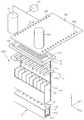
도 16은 본 발명의 유기층 증착 장치의 또 다른 실시예를 개략적으로 도시한 사시도이고, 도 17은 도 16의 유기층 증착 장치의 개략적인 측단면도이고, 도 18은 도 16의 유기층 증착 장치의 개략적인 평단면도이다.FIG. 16 is a perspective view schematically showing another embodiment of the organic layer deposition apparatus of the present invention, FIG. 17 is a schematic side sectional view of the organic layer deposition apparatus of FIG. 16, and FIG. 18 is a schematic Flat section.
도 16 내지 도 18을 참조하면, 본 발명의 또 다른 실시예에 관한 유기층 증착 장치(100")는 증착원(110"), 증착원 노즐부(120"), 차단판 어셈블리(130) 및 패터닝 슬릿(151a)을 포함한다.16 to 18, an organic layer deposition apparatus 100 '' according to another embodiment of the present invention includes an evaporation source 110 '', an evaporation source nozzle unit 120 '', a blocking
여기서, 도 16 내지 도 18에는 설명의 편의를 위해 챔버를 도시하지 않았지만, 도 16 내지 도 18의 모든 구성은 적절한 진공도가 유지되는 챔버 내에 배치되는 것이 바람직하다. 이는 증착 물질의 직진성을 확보하기 위함이다.16 to 18, chambers are not shown for the sake of convenience, but it is preferable that all the arrangements of Figs. 16 to 18 are disposed in a chamber in which an appropriate degree of vacuum is maintained. This is to ensure the straightness of the deposition material.
이러한 챔버 내에는 피 증착체인 기판(500)이 정전척(600)에 의해 이송된다. 상기 기판(500)은 평판 표시장치용 기판이 될 수 있는 데, 다수의 평판 표시장치를 형성할 수 있는 마더 글라스(mother glass)와 같은 대면적 기판이 적용될 수 있다.In this chamber, the
여기서, 본 발명의 일 실시예에서는, 기판(500)이 유기층 증착 장치(100)에 대하여 상대적으로 이동하는 데, 바람직하게는 유기층 증착 장치(100)에 대하여 기판(500)이 A방향으로 이동하도록 할 수 있다.Here, in an embodiment of the present invention, the
전술한 제1실시예와 같이 본 발명의 유기층 증착 장치(100")에서는 종래의 FMM에 비하여 훨씬 작게 패터닝 슬릿 시트(150)를 만들 수 있다. 즉, 본 발명의 유기층 증착 장치(100")의 경우, 기판(500)이 Y축 방향을 따라 이동하면서 연속적으로, 즉 스캐닝(scanning) 방식으로 증착을 수행하기 때문에, 패터닝 슬릿 시트(150)의 X축 방향으로의 폭과 기판(500)의 X축 방향으로의 폭만 실질적으로 동일하게 형성되면, 패터닝 슬릿 시트(150)의 Y축 방향의 길이는 기판(500)의 길이보다 훨씬 작게 형성되어도 무방하게 된다. 물론, 패터닝 슬릿 시트(150)의 X축 방향으로의 폭이 기판(500)의 X축 방향으로의 폭보다 작게 형성되더라도, 기판(500)과 유기층 증착 장치(100")의 상대적 이동에 의한 스캐닝 방식에 의해 충분히 기판(500) 전체에 대하여 증착을 할 수 있게 된다.The
이와 같이, 종래의 FMM에 비하여 훨씬 작게 패터닝 슬릿 시트(150)를 만들 수 있기 때문에, 본 발명의 패터닝 슬릿 시트(150)는 그 제조가 용이하다. 즉, 패터닝 슬릿 시트(150)의 에칭 작업이나, 그 이후의 정밀 인장 및 용접 작업, 이동 및 세정 작업 등 모든 공정에서, 작은 크기의 패터닝 슬릿 시트(150)가 FMM 증착 방법에 비해 유리하다. 또한, 이는 디스플레이 장치가 대형화될수록 더욱 유리하게 된다.As described above, since the
한편, 제1챔버 내에서 상기 기판(500)과 대향 하는 측에는, 증착 물질(115)이 수납 및 가열되는 증착원(110")이 배치된다.On the other hand, on the side facing the
상기 증착원(110")은 그 내부에 증착 물질(115)이 채워지는 도가니(112)와, 이 도가니(112)를 둘러싸는 냉각 블록(111)이 구비된다. 냉각 블록(111)은 도가니(112)로부터의 열이 외부, 즉, 제1챔버 내부로 발산되는 것을 최대한 억제하기 위한 것으로, 이 냉각 블록(111)에는 도가니(112)를 가열시키는 히터(미도시)가 포함되어 있다.The evaporation source 110 'is provided with a
증착원(110")의 일 측, 상세하게는 증착원(110")에서 기판(500)을 향하는 측에는 증착원 노즐부(120")가 배치된다. 그리고 증착원 노즐부(120")에는, X축 방향을 따라서 복수 개의 증착원 노즐(121")들이 형성된다. 여기서, 상기 복수 개의 증착원 노즐(121")들은 등 간격으로 형성될 수 있다. 증착원(110") 내에서 기화된 증착 물질(115)은 이와 같은 증착원 노즐부(120")의 증착원 노즐(121")들을 통과하여 피 증착체인 기판(500) 쪽으로 향하게 되는 것이다.An evaporation source nozzle unit 120 '' is disposed on one side of the evaporation source 110 '', specifically, on the evaporation source 110 '' side facing the
증착원 노즐부(120")의 일 측에는 차단판 어셈블리(130)가 구비된다. 상기 차단판 어셈블리(130)는 복수 개의 차단판(131)들과, 차단판(131)들 외측에 구비되는 차단판 프레임(132)을 포함한다. 상기 복수 개의 차단판(131)들은 X축 방향을 따라서 서로 나란하게 배치될 수 있다. 여기서, 상기 복수 개의 차단판(131)들은 등 간격으로 형성될 수 있다. 또한, 각각의 차단판(131)들은 도면에서 보았을 때 YZ평면을 따라 연장되어 있고, 바람직하게는 직사각형으로 구비될 수 있다. 이와 같이 배치된 복수 개의 차단판(131)들은 증착원 노즐부(120")와 패터닝 슬릿(151a) 사이의 공간을 복수 개의 증착 공간(S)으로 구획한다. 즉, 본 발명의 일 실시예에 관한 유기층 증착 장치(100")는 상기 차단판(131)들에 의하여, 도 17에서 볼 수 있듯이, 증착 물질이 분사되는 각각의 증착원 노즐(121") 별로 증착 공간(S)이 분리된다.A blocking
여기서, 각각의 차단판(131)들은 서로 이웃하고 있는 증착원 노즐(121")들 사이에 배치될 수 있다. 이는 다시 말하면, 서로 이웃하고 있는 차단판(131)들 사이에 하나의 증착원 노즐(121")이 배치되는 것이다. 바람직하게, 증착원 노즐(121)은 서로 이웃하고 있는 차단판(131) 사이의 정 중앙에 위치할 수 있다. 그러나 본 발명은 반드시 이에 한정되지 않으며, 서로 이웃하고 있는 차단판(131)들 사이에 복수의 증착원 노즐(121")이 배치하여도 무방하다. 다만, 이 경우에도 복수의 증착원 노즐(121")들이 서로 이웃하고 있는 차단판(131) 사이의 정 중앙에 위치하도록 하는 것이 바람직하다.Here, each of the blocking
이와 같이, 차단판(131)이 증착원 노즐부(120")와 패터닝 슬릿 시트(150) 사이의 공간을 복수 개의 증착 공간(S)으로 구획함으로써, 하나의 증착원 노즐(121")로부터 배출되는 증착 물질은 다른 증착원 노즐(121")로부터 배출된 증착 물질들과 혼합되지 않고, 패터닝 슬릿(151a)을 통과하여 기판(500)에 증착되는 것이다. 즉, 상기 차단판(131)들은 각 증착원 노즐(121")을 통해 배출되는 증착 물질이 분산되지 않고 직진성을 유지하도록 증착 물질의 Z축 방향의 이동 경로를 가이드 하는 역할을 수행한다.As described above, the blocking
이와 같이, 차단판(131)들을 구비하여 증착 물질의 직진성을 확보함으로써, 기판에 형성되는 음영(shadow)의 크기를 대폭적으로 줄일 수 있으며, 따라서 유기층 증착 장치(100)와 기판(500)을 일정 정도 이격시키는 것이 가능해진다. 이에 대하여는 뒤에서 상세히 기술하기로 한다.The size of the shadow formed on the substrate can be greatly reduced by providing the blocking
한편, 상기 복수 개의 차단판(131)들의 외 측으로는 차단판 프레임(132)이 더 구비될 수 있다. 차단판 프레임(132)은, 복수 개의 차단판(131)들의 측면에 각각 구비되어, 복수 개의 차단판(131)들의 위치를 고정하는 동시에, 증착원 노즐(121)을 통해 배출되는 증착 물질이 Y축 방향으로 분산되지 않도록 증착 물질의 Y축 방향의 이동 경로를 가이드 하는 역할을 수행한다.In addition, a blocking
상기 증착원 노즐부(120")와 차단판 어셈블리(130)는 일정 정도 이격된 것이 바람직하다. 이에 따라, 증착원(110")으로부터 발산되는 열이 차단판 어셈블리(130)에 전도되는 것을 방지할 수 있다. 그러나 본 발명의 사상은 이에 제한되지 아니한다. 즉, 증착원 노즐부(120")와 차단판 어셈블리(130) 사이에 적절한 단열 수단이 구비될 경우 증착원 노즐부(120")와 차단판 어셈블리(130)가 결합하여 접촉할 수도 있을 것이다.It is preferable that the evaporation
한편, 상기 차단판 어셈블리(130)는 유기층 증착 장치(100")로부터 착탈 가능하도록 형성될 수 있다. 본 발명의 일 실시예에 관한 유기층 증착 장치(100")에서는 차단판 어셈블리(130)를 이용하여 증착 공간을 외부 공간과 분리하였기 때문에, 기판(500)에 증착되지 않은 증착 물질은 대부분 차단판 어셈블리(130) 내에 증착된다. 따라서, 차단판 어셈블리(130)를 유기층 증착 장치(100)로부터 착탈가능하도록 형성하여, 장시간 증착 후 차단판 어셈블리(130)에 증착 물질이 많이 쌓이게 되면, 차단판 어셈블리(130)를 유기층 증착 장치(100")로부터 분리하여 별도의 증착 물질 재활용 장치에 넣어서 증착 물질을 회수할 수 있다. 이와 같은 구성을 통하여, 증착 물질 재활용률을 높임으로써 증착 효율이 향상되고 제조 비용이 절감되는 효과를 얻을 수 있다.The blocking
한편, 증착원(110")과 기판(500) 사이에는 패터닝 슬릿 시트(150) 및 프레임(155)이 더 구비된다. 상기 프레임(155)은 대략 창문 틀과 같은 형태로 형성되며, 그 내측에 패터닝 슬릿 시트(150)가 결합한다. 그리고 패터닝 슬릿 시트(150)에는 X축 방향을 따라서 복수 개의 패터닝 슬릿(151a)들이 형성된다. 각 패터닝 슬릿(151a)들은 Y축 방향을 따라 연장되어 있다. 증착원(110) 내에서 기화되어 증착원 노즐(121")을 통과한 증착 물질(115)은 패터닝 슬릿(151a)들을 통과하여 피 증착체인 기판(500) 쪽으로 향하게 된다.A
상기 패터닝 슬릿 시트(150)는 금속 박판으로 형성되고, 인장된 상태에서 프레임(155)에 고정된다. 상기 패터닝 슬릿(151a)은 스트라이프 타입(stripe type)으로 패터닝 슬릿 시트(150)에 에칭을 통해 형성된다.The
여기서, 본 발명의 일 실시예에 관한 유기층 증착 장치(100")는 증착원 노즐(121")들의 총 개수보다 패터닝 슬릿(151a)들의 총 개수가 더 많게 형성된다. 또한, 서로 이웃하고 있는 두 개의 차단판(131) 사이에 배치된 증착원 노즐(121")의 개수보다 패터닝 슬릿(151a)들의 개수가 더 많게 형성된다. 상기 패터닝 슬릿(151a)의 개수는 기판(500)에 형성될 증착 패턴의 개수에 대응되도록 하는 것이 바람직하다.Here, the total number of the patterning slits 151a is formed to be larger than the total number of the evaporation source nozzles 121 '' in the organic layer deposition apparatus 100 '' according to the embodiment of the present invention. The number of the patterning slits 151a is larger than the number of the
한편, 상술한 차단판 어셈블리(130)와 패터닝 슬릿 시트(150)는 서로 일정 정도 이격되도록 형성될 수 있으며, 차단판 어셈블리(130)와 패터닝 슬릿 시트(150)는 별도의 제2연결 부재(133)에 의하여 서로 연결될 수 있다. 상세히, 고온 상태의 증착원(110")에 의해 차단판 어셈블리(130)의 온도는 최대 100℃ 이상 상승하기 때문에, 상승한 차단판 어셈블리(130)의 온도가 패터닝 슬릿 시트(150)로 전도되지 않도록 차단판 어셈블리(130)와 패터닝 슬릿 시트(150)를 일정 정도 이격시키는 것이다.The blocking
상술한 바와 같이, 본 발명의 일 실시예에 관한 유기층 증착 장치(100")는 기판(500)에 대하여 상대적으로 이동하면서 증착을 수행하며, 이와 같이 유기층 증착 장치(100")가 기판(500)에 대하여 상대적으로 이동하기 위해서 패터닝 슬릿 시트(150)는 기판(500)으로부터 일정 정도 이격되도록 형성된다. 그리고 패터닝 슬릿 시트(150)와 기판(500)을 이격시킬 경우 발생하는 음영(shadow) 문제를 해결하기 위하여, 증착원 노즐부(120")와 패터닝 슬릿 시트(150) 사이에 차단판(131)들을 구비하여 증착 물질의 직진성을 확보함으로써, 기판에 형성되는 음영(shadow)의 크기를 대폭적으로 감소시킨 것이다.As described above, the organic
종래의 FMM 증착 방법에서는 기판에 음영(shadow)이 생기지 않도록 하기 위하여 기판에 마스크를 밀착시켜서 증착 공정을 진행하였다. 그러나 이와 같이 기판에 마스크를 밀착시킬 경우, 기판과 마스크 간의 접촉에 의해 기판에 이미 형성되어 있던 패턴들이 긁히는 등 불량 문제가 발생한다는 문제점이 존재하였다. 또한, 마스크를 기판에 대하여 이동시킬 수 없기 때문에, 마스크가 기판과 동일한 크기로 형성되어야 한다. 따라서, 디스플레이 장치가 대형화됨에 따라 마스크의 크기도 커져야 하는데, 이와 같은 대형 마스크를 형성하는 것이 용이하지 아니하다는 문제점이 존재하였다.In the conventional FMM deposition method, a mask is closely adhered to a substrate to prevent a shadow from being formed on the substrate, and a deposition process is performed. However, when the mask is brought into close contact with the substrate, there is a problem that defects such as scratched patterns already formed on the substrate due to contact between the substrate and the mask occur. Further, since the mask can not be moved relative to the substrate, the mask must be formed to have the same size as the substrate. Therefore, as the size of the display device is increased, the size of the mask must be increased. Thus, there is a problem that it is not easy to form such a large mask.
이와 같은 문제점을 해결하기 위하여, 본 발명의 일 실시예에 관한 유기층 증착 장치(100")에서는 패터닝 슬릿 시트(150)가 피 증착체인 기판(500)과 소정 간격을 두고 이격되도록 배치되도록 한다. 이것은 차단판(131)을 구비하여, 기판(500)에 생성되는 음영(shadow)이 작아지게 됨으로써 실현 가능해진다.In order to solve such a problem, in the organic
이와 같은 본 발명에 의해서 패터닝 슬릿 시트를 기판보다 작게 형성한 후, 이 패터닝 슬릿 시트가 기판에 대하여 상대 이동되도록 함으로써, 종래 FMM 방법과 같이 큰 마스크를 제작해야 할 필요가 없게 된 것이다. 또한, 기판과 패터닝 슬릿 시트 사이가 이격되어 있기 때문에, 상호 접촉에 의한 불량을 방지하는 효과를 얻을 수 있다. 또한, 공정에서 기판과 패터닝 슬릿 시트를 밀착시키는 시간이 불필요해지기 때문에, 제조 속도가 향상되는 효과를 얻을 수 있다.According to the present invention, after the patterning slit sheet is formed smaller than the substrate, the patterning slit sheet is moved relative to the substrate, thereby eliminating the need to manufacture a large mask as in the conventional FMM method. In addition, since the substrate and the patterning slit sheet are spaced apart from each other, an effect of preventing defects due to mutual contact can be obtained. In addition, since the time required for the substrate and the patterning slit sheet to adhere to each other in the process becomes unnecessary, the manufacturing speed can be improved.
도 19는 본 발명의 유기층 증착 장치의 또 다른 실시예를 개략적으로 도시한 사시도이다.19 is a perspective view schematically showing still another embodiment of the organic layer deposition apparatus of the present invention.
도 19에 도시된 실시예에 관한 유기층 증착 장치(100''')는 증착원(110"), 증착원 노즐부(120"), 제1 차단판 어셈블리(130), 제2 차단판 어셈블리(140), 패터닝 슬릿 시트(150)를 포함한다.The organic layer deposition apparatus 100 '' 'according to the embodiment shown in FIG. 19 includes an evaporation source 110' ', an evaporation source nozzle unit 120' ', a first
여기서, 도 19에는 설명의 편의를 위해 챔버를 도시하지 않았지만, 도 19의 모든 구성은 적절한 진공도가 유지되는 챔버 내에 배치되는 것이 바람직하다. 이는 증착 물질의 직진성을 확보하기 위함이다.Although the chamber is not shown in FIG. 19 for convenience of explanation, it is preferable that all of the configurations in FIG. 19 are disposed in a chamber in which an appropriate degree of vacuum is maintained. This is to ensure the straightness of the deposition material.
이러한 챔버(미도시) 내에는 피 증착체인 기판(500)이 배치된다. 그리고 챔버(미도시) 내에서 기판(500)과 대향 하는 측에는, 증착 물질(115)이 수납 및 가열되는 증착원(110")이 배치된다.In this chamber (not shown), a
증착원(110") 및 패터닝 슬릿 시트(150)의 상세한 구성은 전술한 도 16에 따른 실시예와 동일하므로 상세한 설명을 생략한다. 그리고 상기 제1차단판 어셈블리(130)는 도 16에 따른 실시예의 차단판 어셈블리와 동일하므로 역시 상세한 설명은 생략한다.The detailed structure of the evaporation source 110 '' and the
본 실시예에서는 제1 차단판 어셈블리(130)의 일 측에 제2 차단판 어셈블리(140)가 구비된다. 상기 제2 차단판 어셈블리(140)는 복수 개의 제2 차단판(141)들과, 제2 차단판(141)들 외측에 구비되는 제2 차단판 프레임(142)을 포함한다.In this embodiment, the second blocking plate assembly 140 is provided on one side of the first
상기 복수 개의 제2 차단판(141)들은 X축 방향을 따라서 서로 나란하게 구비될 수 있다. 그리고 상기 복수 개의 제2 차단판(141)들은 등 간격으로 형성될 수 있다. 또한, 각각의 제2 차단판(141)은 도면에서 보았을 때 YZ평면과 나란하도록, 다시 말하면 X축 방향에 수직이 되도록 형성된다.The plurality of second blocking plates 141 may be provided in parallel with each other along the X-axis direction. The plurality of second blocking plates 141 may be formed at regular intervals. Each second blocking plate 141 is formed so as to be parallel to the YZ plane as viewed in the drawing, that is, perpendicular to the X axis direction.
이와 같이 배치된 복수 개의 제1 차단판(131) 및 제2 차단판(141)들은 증착원 노즐부(120)과 패터닝 슬릿 시트(150) 사이의 공간을 구획하는 역할을 수행한다. 즉, 상기 제1 차단판(131) 및 제2 차단판(141)에 의하여, 증착 물질이 분사되는 각각의 증착원 노즐(121) 별로 증착 공간이 분리되는 것을 일 특징으로 한다.The plurality of
여기서, 각각의 제2 차단판(141)들은 각각의 제1 차단판(131)들과 일대일 대응하도록 배치될 수 있다. 다시 말하면, 각각의 제2 차단판(141)들은 각각의 제1 차단판(131)들과 얼라인(align) 되어 서로 나란하게 배치될 수 있다. 즉, 서로 대응하는 제1 차단판(131)과 제2 차단판(141)은 서로 동일한 평면상에 위치하게 되는 것이다. 도면에는, 제1 차단판(131)의 길이와 제2 차단판(141)의 X축 방향의 폭이 동일한 것으로 도시되어 있지만, 본 발명의 사상은 이에 제한되지 아니한다. 즉, 패터닝 슬릿(151a)과의 정밀한 얼라인(align)이 요구되는 제2 차단판(141)은 상대적으로 얇게 형성되는 반면, 정밀한 얼라인이 요구되지 않는 제1 차단판(131)은 상대적으로 두껍게 형성되어, 그 제조가 용이하도록 하는 것도 가능하다 할 것이다.Here, each of the second blocking plates 141 may be arranged to correspond one-to-one with the respective
이상 설명한 바와 같은 유기층 증착 장치(100''')는 도 1에서 볼 수 있듯이 제1챔버(731) 내에 여러 개가 연속하여 배치될 수 있다. 이 경우, 각 유기층 증착 장치(100)(200)(300)(400)는 서로 다른 증착 물질을 증착하도록 할 수 있으며, 이때, 각 유기층 증착 장치(100)(200)(300)(400)의 패터닝 슬릿의 패턴이 서로 다른 패턴이 되도록 하여, 예컨대 적, 녹, 청색의 화소를 일괄 증착하는 등의 성막 공정을 진행할 수 있다.
As shown in FIG. 1, the organic layer deposition apparatus 100 '''as described above may be continuously arranged in the
도 20은 본 발명의 증착 장치를 이용하여 제조된 액티브 매트릭스형 유기 발광 표시장치의 단면을 도시한 것이다.20 is a cross-sectional view of an active matrix type organic light emitting display device manufactured using the deposition apparatus of the present invention.
도 20은 참조하면, 상기 액티브 매트리스형의 유기 발광 표시 장치는 기판(30) 상에 형성된다. 상기 기판(30)은 투명한 소재, 예컨대 글래스재, 플라스틱재, 또는 금속재로 형성될 수 있다. 상기 기판(30)상에는 전체적으로 버퍼층과 같은 절연막(31)이 형성되어 있다.Referring to FIG. 20, the active matrix type organic light emitting diode display device is formed on a
상기 절연막(31) 상에는 도 19에서 볼 수 있는 바와 같은 TFT(40)와, 커패시터(50)와, 유기 발광 소자(60)가 형성된다.A
상기 절연막(31)의 윗면에는 소정 패턴으로 배열된 반도체 활성층(41)이 형성되어 있다. 상기 반도체 활성층(41)은 게이트 절연막(32)에 의하여 매립되어 있다. 상기 활성층(41)은 p형 또는 n형의 반도체로 구비될 수 있다.On the upper surface of the insulating
상기 게이트 절연막(32)의 윗면에는 커패시터(50)의 제1 커패시터 전극(51)과, 상기 활성층(41)과 대응되는 곳에 TFT(40)의 게이트 전극(42)이 형성된다. 그리고 상기 제1 커패시터 전극(51)과 게이트 전극(42)을 덮도록 층간 절연막(33)이 형성된다. 상기 층간 절연막(33)이 형성된 다음에는 드라이 에칭 등의 식각 공정에 의하여 상기 게이트 절연막(32)과 층간 절연막(33)을 식각하여 콘택 홀을 형성시켜서, 상기 활성층(41)의 일부를 드러나게 한다.A
그 다음으로, 상기 층간 절연막(33) 상에 제2커패시터 전극(52)과 소스/드레인 전극(43)이 형성된다. 상기 소스/드레인 전극(43)은 콘택 홀을 통해 노출된 활성층(41)에 접촉되도록 형성된다. 상기 제2커패시터 전극(52)과 소스/드레인 전극(43)을 덮도록 보호막(34)이 형성되고, 식각 공정을 통하여 상기 드레인 전극(43)의 일부가 드러나도록 한다. 상기 보호막(34) 위로는 보호막(34)의 평탄화를 위해 별도의 절연막을 더 형성할 수도 있다.Next, a
한편, 상기 유기 발광 소자(60)는 전류의 흐름에 따라 적, 녹, 청색의 빛을 발광하여 소정의 화상 정보를 표시하기 위한 것으로서, 상기 보호막(34) 상에 제1전극(61)을 형성한다. 상기 제1전극(61)은 TFT(40)의 드레인 전극(43)과 전기적으로 연결된다.The organic
그리고 상기 제1전극(61)을 덮도록 화소정의막(35)이 형성된다. 이 화소정의막(35)에 소정의 개구(64)를 형성한 후, 이 개구(64)로 한정된 영역 내에 유기 발광막(63)을 형성한다. 유기 발광막(63) 위로는 제2전극(62)을 형성한다.A
상기 화소정의막(35)은 각 화소를 구획하는 것으로, 유기물로 형성되어, 제1전극(61)이 형성되어 있는 기판의 표면, 특히, 보호막(34)의 표면을 평탄화한다.The
상기 제1전극(61)과 제2전극(62)은 서로 절연되어 있으며, 유기 발광막(63)에 서로 다른 극성의 전압을 가해 발광이 이뤄지도록 한다.The
상기 유기 발광막(63)은 저분자 또는 고분자 유기물이 사용될 수 있는 데, 저분자 유기물을 사용할 경우 홀 주입층(HIL: Hole Injection Layer), 홀 수송층(HTL: Hole Transport Layer), 발광층(EML: Emission Layer), 전자 수송층(ETL: Electron Transport Layer), 전자 주입층(EIL: Electron Injection Layer) 등이 단일 혹은 복합의 구조로 적층되어 형성될 수 있으며, 사용 가능한 유기 재료도 구리 프탈로시아닌(CuPc: copper phthalocyanine), N, N-디(나프탈렌-1-일)-N, N'-디페닐-벤지딘 (N, N'-Di(naphthalene-1-yl)-N, N'-diphenyl-benzidine: NPB), 트리스-8-하이드록시퀴놀린 알루미늄(tris-8-hydroxyquinoline aluminum)(Alq3) 등을 비롯해 다양하게 적용 가능하다. 이들 저분자 유기물은 도 1 내지 도 19에서 볼 수 있는 증착 장치 및 증착 소스 유닛(10)을 이용하여 진공증착의 방법으로 형성될 수 있다.When a low-molecular organic material is used, a hole injecting layer (HIL), a hole transporting layer (HTL), a light emitting layer (EML) An electron transport layer (ETL), and an electron injection layer (EIL) may be laminated in a single or a composite structure. The usable organic material may be copper phthalocyanine (CuPc) N-di (naphthalene-1-yl) -N, N'-diphenyl-benzidine: NPB), N, N'- Tris-8-hydroxyquinoline aluminum (Alq3), and the like. These low molecular weight organic materials can be formed by a vacuum deposition method using the deposition apparatus and the deposition source unit 10 shown in Figs. 1 to 19.
먼저, 화소정의막(35)에 개구(64)를 형성한 후, 이 기판(30)을 도 1과 같이 챔버(20)내로 이송한다. 그리고 제1증착 소스(11)와 제2증착 소스(12)에 목표 유기물을 수납한 후, 증착한다. 이때, 호스트와 도펀트를 동시에 증착시킬 경우에는 제1증착 소스(11)와 제2증착 소스(12)에 각각 호스트 물질과 도펀트 물질을 수납하여 증착도록 한다.First, an
이러한 유기 발광막을 형성한 후에는 제2전극(62)을 역시 동일한 증착 공정으로 형성할 수 있다.After the organic light emitting layer is formed, the
한편, 상기 제1전극(61)은 애노드 전극의 기능을 하고, 상기 제2전극(62)은 캐소드 전극의 기능을 할 수 있는 데, 물론, 이들 제1전극(61)과 제2전극(62)의 극성은 반대로 되어도 무방하다. 그리고 제1전극(61)은 각 화소의 영역에 대응되도록 패터닝될 수 있고, 제2전극(62)은 모든 화소를 덮도록 형성될 수 있다.The
상기 제1전극(61)은 투명 전극 또는 반사형 전극으로 구비될 수 있는 데, 투명전극으로 사용될 때에는 ITO, IZO, ZnO, 또는 In2O3로 구비될 수 있고, 반사형 전극으로 사용될 때에는 Ag, Mg, Al, Pt, Pd, Au, Ni, Nd, Ir, Cr, 및 이들의 화합물 등으로 반사층을 형성한 후, 그 위에 ITO, IZO, ZnO, 또는 In2O3로 투명전극층을 형성할 수 있다. 이러한 제1전극(61)은 스퍼터링 방법 등에 의해 성막된 후, 포토 리소그래피법 등에 의해 패터닝된다.The
한편, 상기 제2전극(62)도 투명 전극 또는 반사형 전극으로 구비될 수 있는 데, 투명전극으로 사용될 때에는 이 제2전극(62)이 캐소드 전극으로 사용되므로, 일함수가 작은 금속 즉, Li, Ca, LiF/Ca, LiF/Al, Al, Ag, Mg, 및 이들의 화합물이 유기 발광막(63)의 방향을 향하도록 증착한 후, 그 위에 ITO, IZO, ZnO, 또는 In2O3 등으로 보조 전극층이나 버스 전극 라인을 형성할 수 있다. 그리고 반사형 전극으로 사용될 때에는 위 Li, Ca, LiF/Ca, LiF/Al, Al, Ag, Mg, 및 이들의 화합물을 전면 증착하여 형성한다. 이때, 증착은 전술한 유기 발광막(63)의 경우와 마찬가지의 방법으로 행할 수 있다.When the
본 발명은 이 외에도, 유기 TFT의 유기층 또는 무기막 등의 증착에도 사용할 수 있으며, 기타, 다양한 소재의 성막 공정에 적용 가능하다.In addition, the present invention can be used for deposition of an organic layer or an inorganic film of an organic TFT, and the present invention is applicable to other various film forming processes.
본 발명은 도면에 도시된 실시예를 참고로 설명되었으나 이는 예시적인 것에 불과하며, 본 기술 분야의 통상의 지식을 가진 자라면 이로부터 다양한 변형 및 균등한 다른 실시예가 가능하다는 점을 이해할 것이다. 따라서, 본 발명의 진정한 기술적 보호 범위는 첨부된 특허청구범위의 기술적 사상에 의하여 정해져야 할 것이다.While the present invention has been described with reference to exemplary embodiments, it is to be understood that the invention is not limited to the disclosed exemplary embodiments, but, on the contrary, is intended to cover various modifications and equivalent arrangements included within the spirit and scope of the appended claims. Accordingly, the true scope of the present invention should be determined by the technical idea of the appended claims.
30: 기판31: 절연막
32: 게이트 절연막33: 층간 절연막
34: 보호막35: 화소 정의막
40: TFT50: 커패시터
60: 유기 발광 소자61: 제1 전극
62: 제2 전극63: 유기 발광막
64: 개구
100, 200, 300, 400: 유기층 증착 장치
500: 기판600: 정전척
610: 제1 순환부620: 제2 순환부
710: 로딩부712: 제1래크
718: 제1반전실719: 제1반전 로봇
722: 제2래크726: 반출실
728: 제2반전실729: 제2반전 로봇
730: 증착부731: 제1챔버
732: 제2챔버30: substrate 31: insulating film
32: gate insulating film 33: interlayer insulating film
34: protective film 35: pixel defining film
40: TFT 50: capacitor
60: organic light emitting element 61: first electrode
62: second electrode 63: organic light emitting film
64: aperture
100, 200, 300, 400: Organic layer deposition apparatus
500: substrate 600: electrostatic chuck
610: first circulation unit 620: second circulation unit
710: Loading section 712: First rack
718: first inverting chamber 719: first inverting robot
722: Second rack 726: Discharge chamber
728: second inverting chamber 729: second inverting robot
730: deposition part 731: first chamber
732: Second chamber
Claims (49)
Translated fromKorean증착 물질을 방사하는 증착원;
상기 증착원의 일 측에 배치되며, 제1 방향을 따라 복수 개의 증착원 노즐들이 형성된 증착원 노즐부; 및
상기 증착원 노즐부와 대향되게 배치되고, 상기 제1 방향에 대해 수직인 제2방향을 따라 복수 개의 패터닝 슬릿들이 형성되는 패터닝 슬릿 시트;를 구비하고,
상기 기판이 상기 유기층 증착 장치에 대하여 상기 제1방향을 따라 이동하면서 증착이 수행되고,
상기 패터닝 슬릿 시트는 서로 이격되어 배치되는 제1 얼라인 마크 및 제2 얼라인 마크를 가지며,
상기 기판은 서로 이격되어 배치되는 제1 얼라인 패턴 및 제2 얼라인 패턴을 포함하며,
상기 유기층 증착 장치는 상기 제1 얼라인 마크와 상기 제1 얼라인 패턴을 촬영하는 제1 카메라 어셈블리와, 상기 제2 얼라인 마크와 상기 제2 얼라인 패턴을 촬영하는 제2 카메라 어셈블리를 더 구비하고,
상기 제1 카메라 어셈블리에 의해 촬영된 상기 제1 얼라인 패턴의 영상들이 동일하고, 상기 제2 카메라 어셈블리에 의해 촬영된 상기 제2 얼라인 패턴의 영상들이 동일하도록 상기 기판의 이동 속도와 상기 제1 및 2 카메라 어셈블리의 촬영 속도를 동기화하는 것을 특징으로 하는 유기층 증착 장치.An organic layer deposition apparatus for forming an organic layer on a substrate,
An evaporation source for emitting a deposition material;
An evaporation source nozzle unit disposed at one side of the evaporation source and having a plurality of evaporation source nozzles formed along a first direction; And
And a patterning slit sheet disposed opposite to the evaporation source nozzle portion and having a plurality of patterning slits formed along a second direction perpendicular to the first direction,
The deposition is performed while the substrate moves along the first direction with respect to the organic layer deposition apparatus,
Wherein the patterning slit sheet has a first alignment mark and a second alignment mark spaced apart from each other,
The substrate comprising a first alignment pattern and a second alignment pattern spaced apart from each other,
The organic layer deposition apparatus further includes a first camera assembly for photographing the first alignment mark and the first alignment pattern, and a second camera assembly for photographing the second alignment mark and the second alignment pattern and,
Wherein the images of the first alignment pattern photographed by the first camera assembly are the same and the images of the second alignment pattern photographed by the second camera assembly are the same, And synchronizing the photographing speed of the two camera assemblies.
상기 증착원, 상기 증착원 노즐부 및 상기 패터닝 슬릿 시트는 일체로 형성되는 것을 특징으로 하는 유기층 증착 장치.The method according to claim 1,
Wherein the deposition source, the deposition source nozzle unit, and the patterning slit sheet are integrally formed.
상기 증착원 및 상기 증착원 노즐부와 상기 패터닝 슬릿 시트는 상기 증착 물질의 이동 경로를 가이드 하는 연결 부재에 의해 결합되어 일체로 형성되는 것을 특징으로 하는 유기층 증착 장치.The method according to claim 1,
Wherein the evaporation source, the evaporation source nozzle unit, and the patterning slit sheet are integrally formed by a connection member for guiding the movement path of the evaporation material.
상기 연결 부재는 상기 증착원 및 상기 증착원 노즐부와 상기 패터닝 슬릿 시트 사이의 공간을 외부로부터 밀폐하도록 형성되는 것을 특징으로 하는 유기층 증착 장치The method of claim 3,
Wherein the connecting member is formed to seal the space between the evaporation source and the evaporation source nozzle portion and the patterning slit sheet from the outside.
상기 복수 개의 증착원 노즐들은 소정 각도 틸트 되도록 형성되는 것을 특징으로 하는 유기층 증착 장치.The method according to claim 1,
Wherein the plurality of evaporation source nozzles are formed to be tilted by a predetermined angle.
상기 복수 개의 증착원 노즐들은 상기 제1 방향을 따라 형성된 두 열(列)의 증착원 노즐들을 포함하며, 상기 두 열(列)의 증착원 노즐들은 서로 마주보는 방향으로 틸트되어 있는 것을 특징으로 하는 유기층 증착 장치.6. The method of claim 5,
Wherein the plurality of evaporation source nozzles include two rows of evaporation source nozzles formed along the first direction and the evaporation source nozzles of the two rows are tilted in directions opposite to each other. Organic layer deposition apparatus.
상기 복수 개의 증착원 노즐들은 상기 제1 방향을 따라 형성된 두 열(列)의 증착원 노즐들을 포함하며,
상기 두 열(列)의 증착원 노즐들 중 제1 측에 배치된 증착원 노즐들은 패터닝 슬릿 시트의 제2 측 단부를 바라보도록 배치되고,
상기 두 열(列)의 증착원 노즐들 중 제2 측에 배치된 증착원 노즐들은 패터닝 슬릿 시트의 제1 측 단부를 바라보도록 배치되는 것을 특징으로 하는 유기층 증착 장치.6. The method of claim 5,
Wherein the plurality of evaporation source nozzles include two rows of evaporation source nozzles formed along the first direction,
The evaporation source nozzles disposed on the first one of the two rows of the evaporation source rows are arranged to face the second side edge of the patterning slit sheet,
Wherein the evaporation source nozzles disposed on the second side of the two rows of the evaporation source rows are arranged to face the first side end of the patterning slit sheet.
상기 제1 얼라인 패턴은 상기 제1 방향으로 배열된 복수 개의 제1 마크로 이루어지며,
상기 제2 얼라인 패턴은 상기 제1 방향으로 배열된 복수 개의 제2 마크로 이루어지며,
상기 제1 얼라인 패턴과 상기 제2 얼라인 패턴은 상기 제2 방향으로 이격된 것을 특징으로 하는 유기층 증착 장치.The method according to claim 1,
Wherein the first alignment pattern comprises a plurality of first marks arranged in the first direction,
Wherein the second alignment pattern is formed of a plurality of second marks arranged in the first direction,
Wherein the first alignment pattern and the second alignment pattern are spaced apart from each other in the second direction.
상기 제1 마크와 상기 제2 마크는 모양과 크기가 서로 동일한 것을 특징으로 하는 유기층 증착 장치.9. The method of claim 8,
Wherein the first mark and the second mark have the same shape and size.
상기 제1 마크들 사이의 간격과 상기 제2 마크들 사이의 간격은 서로 동일한 것을 특징으로 하는 유기층 증착 장치.9. The method of claim 8,
Wherein an interval between the first marks and an interval between the second marks are equal to each other.
상기 제1 마크와 상기 제2 마크는 열 십(十)자 형성을 갖는 것을 특징으로 하는 유기층 증착 장치.11. The method of claim 10,
Wherein the first mark and the second mark have a ten-sided character formation.
상기 제1 마크 또는 상기 제2 마크는 다각형으로 이루어진 것을 특징으로 하는 유기층 증착 장치.9. The method of claim 8,
Wherein the first mark or the second mark is formed of a polygonal shape.
상기 제1 마크 또는 상기 제2 마크는 삼각형으로 이루어지는 것을 특징으로 하는 유기층 증착 장치.13. The method of claim 12,
Wherein the first mark or the second mark is a triangle.
상기 제1 얼라인 패턴과 상기 제2 얼라인 패턴은 톱니 형태로 이루어지는 것을 특징으로 하는 유기층 증착 장치.13. The method of claim 12,
Wherein the first alignment pattern and the second alignment pattern are formed in a sawtooth pattern.
상기 기판은 등속도로 상기 제1방향을 따라 이동하고, 상기 제1 카메라 어셈블리와 상기 제2 카메라 어셈블리 각각은 일정한 시간 간격으로 상기 제1 얼라인 패턴과 상기 제2 얼라인 패턴을 촬영하며, 상기 제1 카메라 어셈블리는 동일한 개수의 상기 제1 얼라인 패턴들이 포함된 영상을 촬영하고, 상기 제2 카메라 어셈블리는 동일한 개수의 상기 제2 얼라인 패턴들이 포함된 영상을 촬영하는 것을 특징으로 하는 유기층 증착 장치.The method according to claim 1,
Wherein the substrate moves along the first direction at a constant speed and each of the first camera assembly and the second camera assembly photographs the first alignment pattern and the second alignment pattern at regular time intervals, 1 camera assembly photographs an image including the same number of the first alignment patterns and the second camera assembly photographs an image including the same number of the second alignment patterns. .
상기 제1 카메라 어셈블리와 상기 제2 카메라 어셈블리 각각은 상기 제1 얼라인 마크와 상기 제2 얼라인 마크에 대응하도록 상기 기판 상에 배치되는 것을 특징으로 하는 유기층 증착 장치.The method according to claim 1,
Wherein each of the first camera assembly and the second camera assembly is disposed on the substrate so as to correspond to the first alignment mark and the second alignment mark.
상기 제1 카메라 어셈블리와 상기 제2 카메라 어셈블리에 의해 촬영된 정보를 이용하여 상기 기판과 상기 패터닝 슬릿 시트 사이의 얼라인 정도를 판별하는 제어부를 더 구비한 것을 특징으로 하는 유기층 증착 장치.The method according to claim 1,
Further comprising a control unit for determining the degree of alignment between the substrate and the patterning slit sheet using information captured by the first camera assembly and the second camera assembly.
상기 제어부는 상기 제1 카메라 어셈블리에 의해 촬영된 상기 제1 얼라인 패턴과 상기 제1 얼라인 마크 사이의 제1 간격, 및 상기 제2 카메라 어셈블리에 의해 촬영된 상기 제2 얼라인 패턴과 상기 제2 얼라인 마크 사이의 제2 간격을 비교하여, 상기 패터닝 슬릿 시트와 상기 기판의 상기 제1 방향에 수직한 제2 방향으로의 얼라인을 판별하는 것을 특징으로 하는 유기층 증착 장치.18. The method of claim 17,
Wherein the control unit controls the first camera unit so that the first interval between the first alignment pattern photographed by the first camera assembly and the first alignment mark and the second alignment pattern photographed by the second camera assembly, And the second intervals between the alignment marks are compared to determine alignment in the second direction perpendicular to the first direction of the substrate and the patterning slit sheet.
상기 제어부는 상기 제1 카메라 어셈블리에 의해 촬영된 상기 제1 얼라인 마크와 상기 제2 카메라 어셈블리에 의해 촬영된 상기 제2 얼라인 마크를 비교하여, 상기 제1 방향에 대하여 상기 패터닝 슬릿 시트가 기울어졌는지를 판별하는 것을 특징으로 하는 유기층 증착 장치.18. The method of claim 17,
Wherein the controller compares the first alignment mark photographed by the first camera assembly with the second alignment mark photographed by the second camera assembly to determine whether the patterning slit sheet is inclined with respect to the first direction The organic layer deposition apparatus comprising:
상기 제어부는, 상기 촬영된 제1 얼라인 마크와 상기 촬영된 제2 얼라인 마크의 상기 제1 방향에 있어서의 위치 차이를 판별하고, 상기 촬영된 제1 얼라인 마크를 기준으로 상기 촬영된 제2 얼라인 마크가 앞서 있는 경우, 상기 제1 방향을 기준으로 상기 제1 얼라인 마크 방향으로 기울어진 것으로 판별하며, 상기 촬영된 제1 얼라인 마크를 기준으로 상기 촬영된 제2 얼라인 마크가 뒤에 있는 경우, 상기 제1 방향을 기준으로 상기 촬영된 제2 얼라인 마크 방향으로 기울어진 것으로 판별하는 것을 특징으로 하는 유기층 증착 장치.20. The method of claim 19,
Wherein the control unit discriminates a positional difference between the photographed first alignment mark and the photographed second alignment mark in the first direction, When the second alignment mark is ahead of the second alignment mark, determining that the second alignment mark is inclined toward the first alignment mark with respect to the first direction, Wherein the first alignment mark is inclined in the second alignment mark direction with respect to the first direction.
상기 제어부는 상기 제1 카메라 어셈블리에 의해 촬영된 상기 제1 얼라인 패턴과 상기 제2 카메라 어셈블리에 의해 촬영된 상기 제2 얼라인 패턴를 비교하여, 상기 제1 방향에 대하여 상기 기판이 기울어졌는지를 판별하는 것을 특징으로 하는 유기층 증착 장치.18. The method of claim 17,
The controller compares the first alignment pattern photographed by the first camera assembly and the second alignment pattern photographed by the second camera assembly to determine whether the substrate is inclined with respect to the first direction And the organic layer deposition apparatus.
상기 제어부는, 상기 촬영된 제1 얼라인 패턴과 상기 촬영된 제2 얼라인 패턴의 상기 제1 방향에 있어서의 위치 차이를 판별하고, 상기 촬영된 제1 얼라인 패턴을 기준으로 상기 촬영된 제2 얼라인 패턴이 앞서 있는 경우, 상기 제1 방향을 기준으로 상기 제1 얼라인 패턴 방향으로 기울어진 것으로 판별하며, 상기 촬영된 제1 얼라인 패턴을 기준으로 상기 촬영된 제2 얼라인 패턴이 뒤에 있는 경우, 상기 제1 방향을 기준으로 상기 촬영된 제2 얼라인 패턴 방향으로 기울어진 것으로 판별하는 것을 특징으로 하는 유기층 증착 장치.22. The method of claim 21,
Wherein the control unit discriminates a positional difference between the photographed first alignment pattern and the photographed second alignment pattern in the first direction, When the second alignment pattern is ahead of the first alignment pattern, it is determined that the second alignment pattern is inclined in the first alignment pattern direction with respect to the first direction, The second alignment pattern is inclined in the second alignment pattern direction with respect to the first direction.
상기 제어부에 의해 판별된 상기 얼라인 정도에 따라 상기 기판 또는 상기 패터닝 슬릿 시트를 이동시켜서 상기 기판과 상기 패터닝 슬릿 시트의 얼라인 시키는 것을 특징으로 하는 유기층 증착 장치.18. The method of claim 17,
Wherein the substrate or the patterning slit sheet is moved according to the degree of alignment determined by the controller to align the substrate and the patterning slit sheet.
상기 패터닝 슬릿 시트는 상기 제1 얼라인 마크에서 상기 제1 방향을 따라 이격되어 배치된 제3 얼라인 마크와, 상기 제2 얼라인 마크에서 상기 제1 방향을 따라 이격되어 배치된 제4 얼라인 마크를 더 구비하는 것을 특징으로 하는 유기층 증착 장치.The method according to claim 1,
Wherein the patterning slit sheet includes a third alignment mark disposed at a distance from the first alignment mark in the first direction and a fourth alignment mark spaced apart from the second alignment mark in the first direction, Wherein the organic layer deposition apparatus further comprises a mark.
상기 제1 얼라인 마크와 상기 제3 얼라인 마크 사이의 간격은 상기 제2 얼라인 마크와 상기 제4 얼라인 마크 사이의 간격과 동일한 것을 특징으로 하는 유기층 증착 장치.25. The method of claim 24,
Wherein an interval between the first alignment mark and the third alignment mark is the same as an interval between the second alignment mark and the fourth alignment mark.
상기 제1 얼라인 마크와 상기 제2 얼라인 마크는 상기 제2방향으로 서로 이격되어 있으며, 상기 제3 얼라인 마크와 상기 제4 얼라인 마크는 상기 제2방향으로 서로 이격되어 있는 것을 특징으로 하는 유기층 증착 장치.25. The method of claim 24,
The first alignment mark and the second alignment mark are spaced apart from each other in the second direction and the third alignment mark and the fourth alignment mark are spaced apart from each other in the second direction. Lt; / RTI >
상기 제1 얼라인 마크와 상기 제2 얼라인 마크 사이의 간격은 상기 제3 얼라인 마크와 상기 제4 얼라인 마크 사이의 간격과 동일한 것을 특징으로 하는 유기층 증착 장치.27. The method of claim 26,
Wherein an interval between the first alignment mark and the second alignment mark is equal to a distance between the third alignment mark and the fourth alignment mark.
상기 유기층 증착 장치는 제3 카메라 어셈블리와 제4 카메라 어셈블리를 구비하며, 상기 제3 카메라 어셈블리와 상기 제4 카메라 어셈블리 각각은 상기 제3 얼라인 마크와 상기 제4 얼라인 마크에 대응하도록 상기 기판 상에 배치되는 것을 특징으로 하는 유기층 증착 장치.25. The method of claim 24,
Wherein the organic layer deposition apparatus includes a third camera assembly and a fourth camera assembly, and each of the third camera assembly and the fourth camera assembly includes a third alignment mark and a fourth alignment mark, Wherein the organic layer is deposited on the substrate.
증착 물질을 방사하는 증착원;
상기 증착원의 일 측에 배치되며, 제1 방향을 따라 복수 개의 증착원 노즐들이 형성된 증착원 노즐부;
상기 증착원 노즐부와 대향되게 배치되고, 상기 제1 방향을 따라 복수 개의 패터닝 슬릿들이 배치되는 패터닝 슬릿 시트; 및
상기 증착원 노즐부와 상기 패터닝 슬릿 시트 사이에 상기 제1 방향을 따라 배치되어, 상기 증착원 노즐부와 상기 패터닝 슬릿 시트 사이의 공간을 복수 개의 증착 공간들로 구획하는 복수 개의 차단판들을 구비하는 차단판 어셈블리;를 포함하고,
상기 유기층 증착 장치는 상기 기판과 이격되도록 배치되며,
상기 유기층 증착 장치와 상기 기판은 서로 상대적으로 이동되고,
상기 기판은 서로 이격되어 배치되는 제1 얼라인 패턴 및 제2 얼라인 패턴을 포함하며,
상기 유기층 증착 장치는 상기 제1 얼라인 마크와 상기 제1 얼라인 패턴을 촬영하는 제1 카메라 어셈블리와, 상기 제2 얼라인 마크와 상기 제2 얼라인 패턴을 촬영하는 제2 카메라 어셈블리를 더 구비하고,
상기 제1 카메라 어셈블리에 의해 촬영된 상기 제1 얼라인 패턴의 영상들이 동일하고, 상기 제2 카메라 어셈블리에 의해 촬영된 상기 제2 얼라인 패턴의 영상들이 동일하도록 상기 기판의 이동 속도와 상기 제1 및 2 카메라 어셈블리의 촬영 속도를 동기화하는 것을 특징으로 하는 유기층 증착 장치.An organic layer deposition apparatus for forming an organic layer on a substrate,
An evaporation source for emitting a deposition material;
An evaporation source nozzle unit disposed at one side of the evaporation source and having a plurality of evaporation source nozzles formed along a first direction;
A patterning slit sheet disposed to face the evaporation source nozzle portion and having a plurality of patterning slits arranged along the first direction; And
And a plurality of blocking plates disposed along the first direction between the evaporation source nozzle unit and the patterning slit sheet and partitioning a space between the evaporation source nozzle unit and the patterning slit sheet into a plurality of evaporation spaces A blocking plate assembly,
Wherein the organic layer deposition apparatus is disposed to be spaced apart from the substrate,
Wherein the organic layer deposition apparatus and the substrate are relatively moved with respect to each other,
The substrate comprising a first alignment pattern and a second alignment pattern spaced apart from each other,
The organic layer deposition apparatus further includes a first camera assembly for photographing the first alignment mark and the first alignment pattern, and a second camera assembly for photographing the second alignment mark and the second alignment pattern and,
Wherein the images of the first alignment pattern photographed by the first camera assembly are the same and the images of the second alignment pattern photographed by the second camera assembly are the same, And synchronizing the photographing speed of the two camera assemblies.
상기 복수 개의 차단판들 각각은 상기 제1 방향과 수직인 제2 방향을 따라 연장되도록 형성된 것을 특징으로 하는 유기층 증착 장치.30. The method of claim 29,
Wherein each of the plurality of blocking plates is formed to extend along a second direction perpendicular to the first direction.
상기 차단판 어셈블리는, 복수 개의 제1 차단판들을 구비하는 제1 차단판 어셈블리와, 복수 개의 제2 차단판들을 구비하는 제2 차단판 어셈블리를 포함하는 것을 특징으로 하는 유기층 증착 장치.30. The method of claim 29,
Wherein the blocking plate assembly includes a first blocking plate assembly having a plurality of first blocking plates and a second blocking plate assembly having a plurality of second blocking plates.
상기 복수 개의 제1 차단판들 및 상기 복수 개의 제2 차단판들 각각은 상기 제1 방향과 수직인 제2 방향을 따라 연장되도록 형성된 것을 특징으로 하는 유기층 증착 장치.32. The method of claim 31,
Wherein the plurality of first blocking plates and the plurality of second blocking plates are formed to extend along a second direction perpendicular to the first direction.
상기 복수 개의 제1 차단판들 및 상기 복수 개의 제2 차단판들 각각은 서로 대응되도록 배치되는 것을 특징으로 하는 유기층 증착 장치.33. The method of claim 32,
Wherein the plurality of first blocking plates and the plurality of second blocking plates are arranged to correspond to each other.
상기 제1 얼라인 패턴은 상기 제1 방향으로 배열된 복수 개의 제1 마크로 이루어지며,
상기 제2 얼라인 패턴은 상기 제1 방향으로 배열된 복수 개의 제2 마크로 이루어지며,
상기 제1 얼라인 패턴과 상기 제2 얼라인 패턴은 상기 제1 방향과 수직인 제2 방향으로 이격된 것을 특징으로 하는 유기층 증착 장치.30. The method of claim 29,
Wherein the first alignment pattern comprises a plurality of first marks arranged in the first direction,
Wherein the second alignment pattern is formed of a plurality of second marks arranged in the first direction,
Wherein the first alignment pattern and the second alignment pattern are spaced apart from each other in a second direction perpendicular to the first direction.
상기 제1 마크와 상기 제2 마크는 모양과 크기가 서로 동일한 것을 특징으로 하는 유기층 증착 장치.35. The method of claim 34,
Wherein the first mark and the second mark have the same shape and size.
상기 제1 마크들 사이의 간격과 상기 제2 마크들 사이의 간격은 서로 동일한 것을 특징으로 하는 유기층 증착 장치.35. The method of claim 34,
Wherein an interval between the first marks and an interval between the second marks are equal to each other.
상기 제1 마크와 상기 제2 마크는 열 십(十)자 형성을 갖는 것을 특징으로 하는 유기층 증착 장치.37. The method of claim 36,
Wherein the first mark and the second mark have a ten-sided character formation.
상기 제1 마크 또는 상기 제2 마크는 다각형으로 이루어진 것을 특징으로 하는 유기층 증착 장치.35. The method of claim 34,
Wherein the first mark or the second mark is formed of a polygonal shape.
상기 기판은 등속도로 상기 제1방향을 따라 이동하고, 상기 제1 카메라 어셈블리와 상기 제2 카메라 어셈블리 각각은 일정한 시간 간격으로 상기 제1 얼라인 패턴과 상기 제2 얼라인 패턴을 촬영하며, 상기 제1 카메라 어셈블리는 동일한 개수의 상기 제1 얼라인 패턴들이 포함된 영상을 촬영하고, 상기 제2 카메라 어셈블리는 동일한 개수의 상기 제2 얼라인 패턴들이 포함된 영상을 촬영하는 것을 특징으로 하는 유기층 증착 장치.30. The method of claim 29,
Wherein the substrate moves along the first direction at a constant speed and each of the first camera assembly and the second camera assembly photographs the first alignment pattern and the second alignment pattern at regular time intervals, 1 camera assembly photographs an image including the same number of the first alignment patterns and the second camera assembly photographs an image including the same number of the second alignment patterns. .
상기 제1 카메라 어셈블리와 상기 제2 카메라 어셈블리 각각은 상기 제1 얼라인 마크와 상기 제2 얼라인 마크에 대응하도록 상기 기판 상에 배치되는 것을 특징으로 하는 유기층 증착 장치.30. The method of claim 29,
Wherein each of the first camera assembly and the second camera assembly is disposed on the substrate so as to correspond to the first alignment mark and the second alignment mark.
상기 제1 카메라 어셈블리와 상기 제2 카메라 어셈블리에 의해 촬영된 정보를 이용하여 상기 기판과 상기 패터닝 슬릿 시트 사이의 얼라인 정도를 판별하는 제어부를 더 구비한 것을 특징으로 하는 유기층 증착 장치.30. The method of claim 29,
Further comprising a control unit for determining the degree of alignment between the substrate and the patterning slit sheet using information captured by the first camera assembly and the second camera assembly.
상기 제어부는 상기 제1 카메라 어셈블리에 의해 촬영된 상기 제1 얼라인 패턴과 상기 제1 얼라인 마크 사이의 제1 간격, 및 상기 제2 카메라 어셈블리에 의해 촬영된 상기 제2 얼라인 패턴과 상기 제2 얼라인 마크 사이의 제2 간격을 비교하여, 상기 패터닝 슬릿 시트와 상기 기판의 상기 제1 방향에 수직한 제2 방향으로의 얼라인을 판별하는 것을 특징으로 하는 유기층 증착 장치.42. The method of claim 41,
Wherein the control unit controls the first camera unit so that the first interval between the first alignment pattern photographed by the first camera assembly and the first alignment mark and the second alignment pattern photographed by the second camera assembly, And the second intervals between the alignment marks are compared to determine alignment in the second direction perpendicular to the first direction of the substrate and the patterning slit sheet.
상기 제어부는 상기 제1 카메라 어셈블리에 의해 촬영된 상기 제1 얼라인 마크와 상기 제2 카메라 어셈블리에 의해 촬영된 상기 제2 얼라인 마크를 비교하여, 상기 제1 방향에 대하여 상기 패터닝 슬릿 시트가 기울어졌는지를 판별하는 것을 특징으로 하는 유기층 증착 장치.42. The method of claim 41,
Wherein the controller compares the first alignment mark photographed by the first camera assembly with the second alignment mark photographed by the second camera assembly to determine whether the patterning slit sheet is inclined with respect to the first direction The organic layer deposition apparatus comprising:
상기 제어부는, 상기 촬영된 제1 얼라인 마크와 상기 촬영된 제2 얼라인 마크의 상기 제1 방향에 있어서의 위치 차이를 판별하고, 상기 촬영된 제1 얼라인 마크를 기준으로 상기 촬영된 제2 얼라인 마크가 앞서 있는 경우, 상기 제1 방향을 기준으로 상기 제1 얼라인 마크 방향으로 기울어진 것으로 판별하며, 상기 촬영된 제1 얼라인 마크를 기준으로 상기 촬영된 제2 얼라인 마크가 뒤에 있는 경우, 상기 제1 방향을 기준으로 상기 촬영된 제2 얼라인 마크 방향으로 기울어진 것으로 판별하는 것을 특징으로 하는 유기층 증착 장치.44. The method of claim 43,
Wherein the control unit discriminates a positional difference between the photographed first alignment mark and the photographed second alignment mark in the first direction, When the second alignment mark is ahead of the second alignment mark, determining that the second alignment mark is inclined toward the first alignment mark with respect to the first direction, Wherein the first alignment mark is inclined in the second alignment mark direction with respect to the first direction.
상기 제어부는 상기 제1 카메라 어셈블리에 의해 촬영된 상기 제1 얼라인 패턴과 상기 제2 카메라 어셈블리에 의해 촬영된 상기 제2 얼라인 패턴를 비교하여, 상기 제1 방향에 대하여 상기 기판이 기울어졌는지를 판별하는 것을 특징으로 하는 유기층 증착 장치.42. The method of claim 41,
The controller compares the first alignment pattern photographed by the first camera assembly and the second alignment pattern photographed by the second camera assembly to determine whether the substrate is inclined with respect to the first direction And the organic layer deposition apparatus.
상기 제어부는, 상기 촬영된 제1 얼라인 패턴과 상기 촬영된 제2 얼라인 패턴의 상기 제1 방향에 있어서의 위치 차이를 판별하고, 상기 촬영된 제1 얼라인 패턴을 기준으로 상기 촬영된 제2 얼라인 패턴이 앞서 있는 경우, 상기 제1 방향을 기준으로 상기 제1 얼라인 패턴 방향으로 기울어진 것으로 판별하며, 상기 촬영된 제1 얼라인 패턴을 기준으로 상기 촬영된 제2 얼라인 패턴이 뒤에 있는 경우, 상기 제1 방향을 기준으로 상기 촬영된 제2 얼라인 패턴 방향으로 기울어진 것으로 판별하는 것을 특징으로 하는 유기층 증착 장치.46. The method of claim 45,
Wherein the control unit discriminates a positional difference between the photographed first alignment pattern and the photographed second alignment pattern in the first direction, When the second alignment pattern is ahead of the first alignment pattern, it is determined that the second alignment pattern is inclined in the first alignment pattern direction with respect to the first direction, The second alignment pattern is inclined in the second alignment pattern direction with respect to the first direction.
상기 제어부에 의해 판별된 상기 얼라인 정도에 따라 상기 기판 또는 상기 패터닝 슬릿 시트를 이동시켜서 상기 기판과 상기 패터닝 슬릿 시트의 얼라인 시키는 것을 특징으로 하는 유기층 증착 장치.42. The method of claim 41,
Wherein the substrate or the patterning slit sheet is moved according to the degree of alignment determined by the controller to align the substrate and the patterning slit sheet.
상기 패터닝 슬릿 시트는 상기 제1 얼라인 마크에서 상기 제1 방향을 따라 이격되어 배치된 제3 얼라인 마크와, 상기 제2 얼라인 마크에서 상기 제1 방향을 따라 이격되어 배치된 제4 얼라인 마크를 더 구비하는 것을 특징으로 하는 유기층 증착 장치.30. The method of claim 29,
Wherein the patterning slit sheet includes a third alignment mark disposed at a distance from the first alignment mark in the first direction and a fourth alignment mark spaced apart from the second alignment mark in the first direction, Wherein the organic layer deposition apparatus further comprises a mark.
상기 유기층 증착 장치는 제3 카메라 어셈블리와 제4 카메라 어셈블리를 구비하며, 상기 제3 카메라 어셈블리와 상기 제4 카메라 어셈블리 각각은 상기 제3 얼라인 마크와 상기 제4 얼라인 마크에 대응하도록 상기 기판 상에 배치되는 것을 특징으로 하는 유기층 증착 장치.49. The method of claim 48,
Wherein the organic layer deposition apparatus includes a third camera assembly and a fourth camera assembly, and each of the third camera assembly and the fourth camera assembly includes a third alignment mark and a fourth alignment mark, Wherein the organic layer is deposited on the substrate.
Priority Applications (5)
| Application Number | Priority Date | Filing Date | Title |
|---|---|---|---|
| KR1020110066125AKR101826068B1 (en) | 2011-07-04 | 2011-07-04 | Apparatus for thin layer deposition |
| US13/467,998US8951610B2 (en) | 2011-07-04 | 2012-05-09 | Organic layer deposition apparatus |
| TW101118074ATWI664724B (en) | 2011-07-04 | 2012-05-21 | Organic layer deposition apparatus |
| CN201210216700.5ACN102867919B (en) | 2011-07-04 | 2012-06-27 | Organic layer depositing device |
| JP2012149280AJP5992741B2 (en) | 2011-07-04 | 2012-07-03 | Organic layer deposition equipment |
Applications Claiming Priority (1)
| Application Number | Priority Date | Filing Date | Title |
|---|---|---|---|
| KR1020110066125AKR101826068B1 (en) | 2011-07-04 | 2011-07-04 | Apparatus for thin layer deposition |
Publications (2)
| Publication Number | Publication Date |
|---|---|
| KR20130004831A KR20130004831A (en) | 2013-01-14 |
| KR101826068B1true KR101826068B1 (en) | 2018-02-07 |
Family
ID=47437871
Family Applications (1)
| Application Number | Title | Priority Date | Filing Date |
|---|---|---|---|
| KR1020110066125AActiveKR101826068B1 (en) | 2011-07-04 | 2011-07-04 | Apparatus for thin layer deposition |
Country Status (5)
| Country | Link |
|---|---|
| US (1) | US8951610B2 (en) |
| JP (1) | JP5992741B2 (en) |
| KR (1) | KR101826068B1 (en) |
| CN (1) | CN102867919B (en) |
| TW (1) | TWI664724B (en) |
Families Citing this family (31)
| Publication number | Priority date | Publication date | Assignee | Title |
|---|---|---|---|---|
| US8882920B2 (en)* | 2009-06-05 | 2014-11-11 | Samsung Display Co., Ltd. | Thin film deposition apparatus |
| JP5328726B2 (en) | 2009-08-25 | 2013-10-30 | 三星ディスプレイ株式會社 | Thin film deposition apparatus and organic light emitting display device manufacturing method using the same |
| JP5677785B2 (en) | 2009-08-27 | 2015-02-25 | 三星ディスプレイ株式會社Samsung Display Co.,Ltd. | Thin film deposition apparatus and organic light emitting display device manufacturing method using the same |
| US8876975B2 (en) | 2009-10-19 | 2014-11-04 | Samsung Display Co., Ltd. | Thin film deposition apparatus |
| KR101084184B1 (en) | 2010-01-11 | 2011-11-17 | 삼성모바일디스플레이주식회사 | Thin film deposition apparatus |
| KR101193186B1 (en) | 2010-02-01 | 2012-10-19 | 삼성디스플레이 주식회사 | Apparatus for thin layer deposition, method for manufacturing of organic light emitting display apparatus using the same, and organic light emitting display apparatus manufactured by the method |
| KR101156441B1 (en) | 2010-03-11 | 2012-06-18 | 삼성모바일디스플레이주식회사 | Apparatus for thin layer deposition |
| US8894458B2 (en) | 2010-04-28 | 2014-11-25 | Samsung Display Co., Ltd. | Thin film deposition apparatus, method of manufacturing organic light-emitting display device by using the apparatus, and organic light-emitting display device manufactured by using the method |
| KR101223723B1 (en) | 2010-07-07 | 2013-01-18 | 삼성디스플레이 주식회사 | Apparatus for thin layer deposition, method for manufacturing of organic light emitting display apparatus using the same, and organic light emitting display apparatus manufactured by the method |
| KR101723506B1 (en) | 2010-10-22 | 2017-04-19 | 삼성디스플레이 주식회사 | Apparatus for organic layer deposition and method for manufacturing of organic light emitting display apparatus using the same |
| KR101738531B1 (en) | 2010-10-22 | 2017-05-23 | 삼성디스플레이 주식회사 | Method for manufacturing of organic light emitting display apparatus, and organic light emitting display apparatus manufactured by the method |
| KR20120045865A (en) | 2010-11-01 | 2012-05-09 | 삼성모바일디스플레이주식회사 | Apparatus for organic layer deposition |
| KR20120065789A (en) | 2010-12-13 | 2012-06-21 | 삼성모바일디스플레이주식회사 | Apparatus for organic layer deposition |
| KR101760897B1 (en) | 2011-01-12 | 2017-07-25 | 삼성디스플레이 주식회사 | Deposition source and apparatus for organic layer deposition having the same |
| JP2014515789A (en)* | 2011-04-20 | 2014-07-03 | コーニンクレッカ フィリップス エヌ ヴェ | Measuring apparatus and method for vapor deposition applications |
| KR101840654B1 (en) | 2011-05-25 | 2018-03-22 | 삼성디스플레이 주식회사 | Apparatus for organic layer deposition and method for manufacturing of organic light emitting display apparatus using the same |
| KR101852517B1 (en) | 2011-05-25 | 2018-04-27 | 삼성디스플레이 주식회사 | Apparatus for organic layer deposition and method for manufacturing of organic light emitting display apparatus using the same |
| KR101857249B1 (en) | 2011-05-27 | 2018-05-14 | 삼성디스플레이 주식회사 | Patterning slit sheet assembly, apparatus for organic layer deposition, method for manufacturing organic light emitting display apparatus and organic light emitting display apparatus |
| KR101826068B1 (en) | 2011-07-04 | 2018-02-07 | 삼성디스플레이 주식회사 | Apparatus for thin layer deposition |
| KR102013318B1 (en)* | 2012-09-20 | 2019-08-23 | 삼성디스플레이 주식회사 | Apparatus for thin layer deposition, method for manufacturing of organic light emitting display apparatus using the same, and organic light emitting display apparatus |
| KR102489065B1 (en)* | 2013-03-15 | 2023-01-13 | 어플라이드 머티어리얼스, 인코포레이티드 | Position and temperature monitoring of ald platen susceptor |
| KR102058515B1 (en) | 2013-04-18 | 2019-12-24 | 삼성디스플레이 주식회사 | Deposition apparatus, method for manufacturing organic light emitting display apparatus using the same, and organic light emitting display apparatus manufactured by the same |
| KR102075995B1 (en)* | 2013-04-30 | 2020-02-11 | 삼성전자주식회사 | Method of formation electrode by using metal mask |
| KR102113581B1 (en)* | 2013-05-22 | 2020-05-22 | 삼성디스플레이 주식회사 | Apparatus for deposition, method thereof and method for forming quntum-dot layer using the same |
| KR102086550B1 (en) | 2013-05-31 | 2020-03-10 | 삼성디스플레이 주식회사 | Deposition apparatus, method for manufacturing organic light emitting display apparatus using the same, and organic light emitting display apparatus manufactured by the same |
| KR102069189B1 (en)* | 2013-06-17 | 2020-01-23 | 삼성디스플레이 주식회사 | Apparatus for organic layer deposition, and method for manufacturing of organic light emitting display apparatus using the same |
| KR102366569B1 (en)* | 2015-07-01 | 2022-02-25 | 삼성디스플레이 주식회사 | Mask tension welding device for thin film deposition |
| CN105887010B (en) | 2016-05-13 | 2018-10-26 | 京东方科技集团股份有限公司 | Mask integrated framework and evaporated device |
| TWI604073B (en)* | 2016-08-09 | 2017-11-01 | 盟立自動化股份有限公司 | Mask structure capable of calibrating an image capturing module and adapted for a evaporation process of an organic light-emitting diode |
| JP7172151B2 (en)* | 2018-06-11 | 2022-11-16 | オムロン株式会社 | Control systems, controllers and programs |
| CN110597360B (en)* | 2019-10-25 | 2021-09-14 | 业成科技(成都)有限公司 | Method for bonding glass cover plate of curved display |
Citations (1)
| Publication number | Priority date | Publication date | Assignee | Title |
|---|---|---|---|---|
| WO2011034011A1 (en) | 2009-09-15 | 2011-03-24 | シャープ株式会社 | Vapor deposition method and vapor deposition apparatus |
Family Cites Families (462)
| Publication number | Priority date | Publication date | Assignee | Title |
|---|---|---|---|---|
| JPS6053745B2 (en) | 1981-07-31 | 1985-11-27 | アルバツク成膜株式会社 | Method for forming heterogeneous optical thin films by binary deposition |
| JPS5959237U (en) | 1982-10-15 | 1984-04-18 | 鐘通工業株式会社 | Switchable permanent magnetic chuck |
| KR890002747B1 (en) | 1983-11-07 | 1989-07-26 | 가부시기가이샤 히다찌세이사꾸쇼 | Film deposition method using ion beam and apparatus therefor |
| JPH0682642B2 (en) | 1985-08-09 | 1994-10-19 | 株式会社日立製作所 | Surface treatment equipment |
| US4792378A (en) | 1987-12-15 | 1988-12-20 | Texas Instruments Incorporated | Gas dispersion disk for use in plasma enhanced chemical vapor deposition reactor |
| JPH02247372A (en) | 1989-03-17 | 1990-10-03 | Mitsubishi Electric Corp | Thin film deposition method |
| JPH0827568B2 (en) | 1990-07-02 | 1996-03-21 | 三田工業株式会社 | Transfer paper separating device in image forming apparatus |
| JP3125279B2 (en) | 1991-02-25 | 2001-01-15 | 東海カーボン株式会社 | Graphite crucible for vacuum evaporation |
| JP2572861Y2 (en) | 1991-05-13 | 1998-05-25 | テイエチケー株式会社 | Slide unit for linear motion |
| JP2797233B2 (en) | 1992-07-01 | 1998-09-17 | 富士通株式会社 | Thin film growth equipment |
| FR2695943B1 (en) | 1992-09-18 | 1994-10-14 | Alsthom Cge Alcatel | Process for the vapor phase deposition of a fluorinated glass film on a substrate. |
| JP3395801B2 (en) | 1994-04-28 | 2003-04-14 | 株式会社ニコン | Catadioptric projection optical system, scanning projection exposure apparatus, and scanning projection exposure method |
| US6045671A (en) | 1994-10-18 | 2000-04-04 | Symyx Technologies, Inc. | Systems and methods for the combinatorial synthesis of novel materials |
| JP3401356B2 (en) | 1995-02-21 | 2003-04-28 | パイオニア株式会社 | Organic electroluminescent display panel and method of manufacturing the same |
| JPH1050478A (en) | 1996-04-19 | 1998-02-20 | Toray Ind Inc | Organic electroluminescent device and method of manufacturing the same |
| CH691680A5 (en) | 1996-10-15 | 2001-09-14 | Unaxis Deutschland Gmbh | Transport apparatus for workpieces in a vacuum system. |
| US6091195A (en) | 1997-02-03 | 2000-07-18 | The Trustees Of Princeton University | Displays having mesa pixel configuration |
| US6274198B1 (en) | 1997-02-24 | 2001-08-14 | Agere Systems Optoelectronics Guardian Corp. | Shadow mask deposition |
| JPH10270535A (en) | 1997-03-25 | 1998-10-09 | Nikon Corp | Moving stage device and circuit device manufacturing method using the stage device |
| KR100257219B1 (en) | 1997-10-23 | 2000-05-15 | 박용관 | Method and device for making a safety operation of a polyethylene gas pipe valve arrangement |
| JP3948082B2 (en) | 1997-11-05 | 2007-07-25 | カシオ計算機株式会社 | Method for manufacturing organic electroluminescence element |
| US6337102B1 (en) | 1997-11-17 | 2002-01-08 | The Trustees Of Princeton University | Low pressure vapor phase deposition of organic thin films |
| US6099649A (en) | 1997-12-23 | 2000-08-08 | Applied Materials, Inc. | Chemical vapor deposition hot-trap for unreacted precursor conversion and effluent removal |
| JP2000068054A (en) | 1998-08-26 | 2000-03-03 | Hokuriku Electric Ind Co Ltd | Manufacture of el element |
| KR20000019254A (en) | 1998-09-08 | 2000-04-06 | 석창길 | Device for improving thin film thickness uniformity of cvd |
| US6280821B1 (en) | 1998-09-10 | 2001-08-28 | Ppg Industries Ohio, Inc. | Reusable mask and method for coating substrate |
| US6384529B2 (en) | 1998-11-18 | 2002-05-07 | Eastman Kodak Company | Full color active matrix organic electroluminescent display panel having an integrated shadow mask |
| CA2374448A1 (en) | 1999-01-26 | 2000-08-03 | Dbs Beschichtung Und Systeme-Technik Gmbh | Method for coating the inside of pipes and coating system |
| US6610150B1 (en) | 1999-04-02 | 2003-08-26 | Asml Us, Inc. | Semiconductor wafer processing system with vertically-stacked process chambers and single-axis dual-wafer transfer system |
| JP3734239B2 (en) | 1999-04-02 | 2006-01-11 | キヤノン株式会社 | Organic film vacuum deposition mask regeneration method and apparatus |
| JP4136185B2 (en) | 1999-05-12 | 2008-08-20 | パイオニア株式会社 | Organic electroluminescent multicolor display and method for manufacturing the same |
| US6469439B2 (en) | 1999-06-15 | 2002-10-22 | Toray Industries, Inc. | Process for producing an organic electroluminescent device |
| EP1115268A1 (en) | 1999-07-07 | 2001-07-11 | Sony Corporation | Method and apparatus for manufacturing flexible organic el display |
| JP2001052862A (en) | 1999-08-04 | 2001-02-23 | Hokuriku Electric Ind Co Ltd | Manufacture of organic el element and device therefor |
| JP4352522B2 (en) | 1999-09-01 | 2009-10-28 | ソニー株式会社 | Light-emitting flat display element |
| JP4187367B2 (en) | 1999-09-28 | 2008-11-26 | 三洋電機株式会社 | ORGANIC LIGHT EMITTING ELEMENT, ITS MANUFACTURING DEVICE, AND ITS MANUFACTURING METHOD |
| KR20010050711A (en) | 1999-09-29 | 2001-06-15 | 준지 키도 | Organic electroluminescent device, group of organic electroluminescent devices and controlling method of emission spectrum in such devices |
| KR100302159B1 (en) | 1999-10-29 | 2001-09-22 | 최중호 | Scent diffusion apparatus and method therefor |
| WO2001030404A1 (en) | 1999-10-29 | 2001-05-03 | E. One Co., Ltd. | Scent diffusion apparatus and method thereof |
| KR20010039298A (en) | 1999-10-29 | 2001-05-15 | 김영남 | Field emission display |
| KR100388903B1 (en) | 1999-12-10 | 2003-06-25 | 삼성에스디아이 주식회사 | Shadow mask frame assembly for the flat CRT |
| JP2001185350A (en) | 1999-12-24 | 2001-07-06 | Sanyo Electric Co Ltd | Worn mask, its manufacturing method, electroluminescent display device and its manufacturing method |
| TW490714B (en) | 1999-12-27 | 2002-06-11 | Semiconductor Energy Lab | Film formation apparatus and method for forming a film |
| KR100653515B1 (en) | 1999-12-30 | 2006-12-04 | 주식회사 팬택앤큐리텔 | Terminal of mobile communication system |
| JP3754859B2 (en) | 2000-02-16 | 2006-03-15 | キヤノン株式会社 | Manufacturing method of image display device |
| US20030021886A1 (en) | 2000-02-23 | 2003-01-30 | Baele Stephen James | Method of printing and printing machine |
| KR20010092914A (en) | 2000-03-27 | 2001-10-27 | 윤종용 | Electrical static chuck comprising a shadow ring |
| JP3802309B2 (en) | 2000-03-28 | 2006-07-26 | 株式会社アドテックエンジニアリング | Positioning apparatus and exposure apparatus in multilayer circuit board manufacture |
| JP4053209B2 (en) | 2000-05-01 | 2008-02-27 | 三星エスディアイ株式会社 | Manufacturing method of organic EL display |
| TW593622B (en) | 2000-05-19 | 2004-06-21 | Eastman Kodak Co | Method of using predoped materials for making an organic light-emitting device |
| EP1167566B1 (en) | 2000-06-22 | 2011-01-26 | Panasonic Electric Works Co., Ltd. | Apparatus for and method of vacuum vapor deposition |
| KR20020000201A (en) | 2000-06-23 | 2002-01-05 | 최승락 | Method cleaning Liquid Chrystal Display using Laser and Vapor Phase |
| US6673386B2 (en) | 2000-06-29 | 2004-01-06 | Matsushita Electric Industrial Co., Ltd. | Method and apparatus for forming pattern onto panel substrate |
| TW451601B (en) | 2000-08-07 | 2001-08-21 | Ind Tech Res Inst | The fabrication method of full color organic electroluminescent device |
| JP2002099095A (en) | 2000-09-25 | 2002-04-05 | Orc Mfg Co Ltd | Automatic both-side exposing device and method of using the same |
| JP2002175878A (en) | 2000-09-28 | 2002-06-21 | Sanyo Electric Co Ltd | Layer forming method and color light emitting device manufacturing method |
| TW594395B (en) | 2000-09-29 | 2004-06-21 | Nippon Zeon Co | Photoresist composition for insulating film, insulating film for organic electroluminescent element, and process for producing the same |
| KR100726132B1 (en) | 2000-10-31 | 2007-06-12 | 엘지.필립스 엘시디 주식회사 | Array substrate for liquid crystal display device and manufacturing method |
| US7078070B2 (en) | 2000-11-07 | 2006-07-18 | Helix Technology Inc. | Method for fabricating an organic light emitting diode |
| JP3770074B2 (en)* | 2000-11-10 | 2006-04-26 | 三菱電機株式会社 | Metal mask alignment system |
| US6468496B2 (en) | 2000-12-21 | 2002-10-22 | Arco Chemical Technology, L.P. | Process for producing hydrogen peroxide |
| KR100625403B1 (en) | 2000-12-22 | 2006-09-18 | 주식회사 하이닉스반도체 | Virtual Channel SDRAM |
| KR100698033B1 (en) | 2000-12-29 | 2007-03-23 | 엘지.필립스 엘시디 주식회사 | Organic electroluminescent device and manufacturing method thereof |
| US6558735B2 (en) | 2001-04-20 | 2003-05-06 | Eastman Kodak Company | Reusable mass-sensor in manufacture of organic light-emitting devices |
| KR100405080B1 (en) | 2001-05-11 | 2003-11-10 | 엘지.필립스 엘시디 주식회사 | A method of crystallizing Si |
| KR100463212B1 (en) | 2001-05-19 | 2004-12-23 | 주식회사 아이엠티 | Apparatus for dry surface-cleaning of materials |
| JP4704605B2 (en) | 2001-05-23 | 2011-06-15 | 淳二 城戸 | Continuous vapor deposition apparatus, vapor deposition apparatus and vapor deposition method |
| KR20020091457A (en) | 2001-05-30 | 2002-12-06 | 주식회사 현대 디스플레이 테크놀로지 | Method for control color property of tft-lcd |
| US20020197393A1 (en) | 2001-06-08 | 2002-12-26 | Hideaki Kuwabara | Process of manufacturing luminescent device |
| KR100406059B1 (en) | 2001-06-22 | 2003-11-17 | 미래산업 주식회사 | Transfer for Tray Feeder |
| JP2003077662A (en) | 2001-06-22 | 2003-03-14 | Junji Kido | Method and device for manufacturing organic electroluminescent element |
| JP2003003250A (en) | 2001-06-22 | 2003-01-08 | Alps Electric Co Ltd | Vacuum deposition polymerization system and method for depositing organic film using the system |
| KR100732742B1 (en) | 2001-06-27 | 2007-06-27 | 주식회사 하이닉스반도체 | Focus monitoring method |
| US6483690B1 (en) | 2001-06-28 | 2002-11-19 | Lam Research Corporation | Ceramic electrostatic chuck assembly and method of making |
| US6554969B1 (en) | 2001-07-11 | 2003-04-29 | Advanced Micro Devices, Inc. | Acoustically enhanced deposition processes, and systems for performing same |
| JP3705237B2 (en) | 2001-09-05 | 2005-10-12 | ソニー株式会社 | Display device manufacturing system and method using organic electroluminescent element |
| KR200257218Y1 (en) | 2001-09-07 | 2001-12-24 | 엘지.필립스 엘시디 주식회사 | Mask apparatus for organic electro-luminescence device |
| KR100437768B1 (en) | 2001-09-13 | 2004-06-30 | 엘지전자 주식회사 | Thin Film Sputtering Device |
| US20090208754A1 (en) | 2001-09-28 | 2009-08-20 | Vitex Systems, Inc. | Method for edge sealing barrier films |
| TW591202B (en) | 2001-10-26 | 2004-06-11 | Hermosa Thin Film Co Ltd | Dynamic film thickness control device/method and ITS coating method |
| KR100730111B1 (en) | 2001-10-26 | 2007-06-19 | 삼성에스디아이 주식회사 | Frame for mask of organic EL element |
| KR100430336B1 (en) | 2001-11-16 | 2004-05-03 | 정광호 | Apparatus for manufacturing organic electro-luminescent light emitting devices for mass production |
| KR100450978B1 (en) | 2001-11-26 | 2004-10-02 | 주성엔지니어링(주) | electrostatic chuck |
| US20030101937A1 (en) | 2001-11-28 | 2003-06-05 | Eastman Kodak Company | Thermal physical vapor deposition source for making an organic light-emitting device |
| JP2003159786A (en) | 2001-11-28 | 2003-06-03 | Seiko Epson Corp | Discharge method and apparatus, electro-optical apparatus, method for manufacturing the same and apparatus for manufacturing the same, color filter, method for manufacturing the same and apparatus for manufacturing the same, device having base material, method for manufacturing the same, and apparatus for manufacturing the same |
| KR100490534B1 (en) | 2001-12-05 | 2005-05-17 | 삼성에스디아이 주식회사 | Mask frame assembly for thin layer vacuum evaporation of Organic electro luminescence device |
| SG114589A1 (en) | 2001-12-12 | 2005-09-28 | Semiconductor Energy Lab | Film formation apparatus and film formation method and cleaning method |
| TW200305773A (en) | 2001-12-26 | 2003-11-01 | Pentax Corp | Projection Aligner |
| US20090169868A1 (en) | 2002-01-29 | 2009-07-02 | Vanderbilt University | Methods and apparatus for transferring a material onto a substrate using a resonant infrared pulsed laser |
| US6897164B2 (en) | 2002-02-14 | 2005-05-24 | 3M Innovative Properties Company | Aperture masks for circuit fabrication |
| US6919139B2 (en) | 2002-02-14 | 2005-07-19 | E. I. Du Pont De Nemours And Company | Electroluminescent iridium compounds with phosphinoalkoxides and phenylpyridines or phenylpyrimidines and devices made with such compounds |
| KR100595310B1 (en) | 2002-02-22 | 2006-07-03 | 엘지.필립스 엘시디 주식회사 | Mask Fixing Device and Checking Device Using It |
| US7006202B2 (en) | 2002-02-21 | 2006-02-28 | Lg.Philips Lcd Co., Ltd. | Mask holder for irradiating UV-rays |
| US20030168013A1 (en) | 2002-03-08 | 2003-09-11 | Eastman Kodak Company | Elongated thermal physical vapor deposition source with plural apertures for making an organic light-emitting device |
| JP2003297562A (en) | 2002-03-29 | 2003-10-17 | Sanyo Electric Co Ltd | Vapor deposition method |
| KR100501306B1 (en) | 2002-04-01 | 2005-07-18 | (주) 휴네텍 | method of manufacturing a light guiding panel and an apparatus for the same, and a particle blasting apparatus for manufacturing the light guiding panel |
| KR100469252B1 (en) | 2002-04-12 | 2005-02-02 | 엘지전자 주식회사 | Shadow Mask and Full Color Organic Electroluminescence Display Device Using the same |
| US6749906B2 (en) | 2002-04-25 | 2004-06-15 | Eastman Kodak Company | Thermal physical vapor deposition apparatus with detachable vapor source(s) and method |
| ATE481982T1 (en) | 2002-05-03 | 2010-10-15 | Us Gov Health & Human Serv | DENGUE VACCINE WITH A COMMON 30 NUCLEOTIDE DELETION IN THE 3'UTR OF DENGUE TYPES 1 AND 2. |
| US20030232563A1 (en) | 2002-05-09 | 2003-12-18 | Isao Kamiyama | Method and apparatus for manufacturing organic electroluminescence device, and system and method for manufacturing display unit using organic electroluminescence devices |
| JP4292777B2 (en) | 2002-06-17 | 2009-07-08 | ソニー株式会社 | Thin film forming equipment |
| US20030221620A1 (en) | 2002-06-03 | 2003-12-04 | Semiconductor Energy Laboratory Co., Ltd. | Vapor deposition device |
| US6955726B2 (en) | 2002-06-03 | 2005-10-18 | Samsung Sdi Co., Ltd. | Mask and mask frame assembly for evaporation |
| KR100908232B1 (en) | 2002-06-03 | 2009-07-20 | 삼성모바일디스플레이주식회사 | Mask frame assembly for thin film deposition of organic electroluminescent device |
| MY164487A (en) | 2002-07-11 | 2017-12-29 | Molecular Imprints Inc | Step and repeat imprint lithography processes |
| JP2004043898A (en) | 2002-07-12 | 2004-02-12 | Canon Electronics Inc | Vapor deposition mask, and organic electroluminescence display device |
| JP2004069414A (en) | 2002-08-05 | 2004-03-04 | Nec Corp | Method for measuring gap between mask and substrate of plasma display panel |
| KR100397196B1 (en) | 2002-08-27 | 2003-09-13 | 에이엔 에스 주식회사 | Organic material point source feeding unit in organic semiconductor device and method thereof |
| JP2004103269A (en) | 2002-09-05 | 2004-04-02 | Sanyo Electric Co Ltd | Manufacture method for organic electroluminescence display device |
| TWI252706B (en) | 2002-09-05 | 2006-04-01 | Sanyo Electric Co | Manufacturing method of organic electroluminescent display device |
| JP2004103341A (en) | 2002-09-09 | 2004-04-02 | Matsushita Electric Ind Co Ltd | Method for manufacturing organic electroluminescence device |
| US20040123804A1 (en) | 2002-09-20 | 2004-07-01 | Semiconductor Energy Laboratory Co., Ltd. | Fabrication system and manufacturing method of light emitting device |
| US6911671B2 (en) | 2002-09-23 | 2005-06-28 | Eastman Kodak Company | Device for depositing patterned layers in OLED displays |
| US20040086639A1 (en) | 2002-09-24 | 2004-05-06 | Grantham Daniel Harrison | Patterned thin-film deposition using collimating heated mask asembly |
| JP4139186B2 (en) | 2002-10-21 | 2008-08-27 | 東北パイオニア株式会社 | Vacuum deposition equipment |
| JP2004143521A (en) | 2002-10-24 | 2004-05-20 | Sony Corp | Thin-film deposition device |
| KR100504477B1 (en) | 2002-11-05 | 2005-08-03 | 엘지전자 주식회사 | Heating source apparatus for Organic electron luminescence |
| KR100532657B1 (en) | 2002-11-18 | 2005-12-02 | 주식회사 야스 | Apparatus for controlling deposition zone of homogeneously mixed layer in multi source co-deposition |
| JP4072422B2 (en) | 2002-11-22 | 2008-04-09 | 三星エスディアイ株式会社 | Deposition mask structure, method for producing the same, and method for producing organic EL element using the same |
| JP2004225058A (en) | 2002-11-29 | 2004-08-12 | Sony Corp | Film deposition apparatus, display panel manufacturing apparatus, and method for the same |
| JP2004183044A (en) | 2002-12-03 | 2004-07-02 | Seiko Epson Corp | Mask evaporation method and apparatus, mask and mask manufacturing method, display panel manufacturing apparatus, display panel, and electronic equipment |
| JP2004199919A (en) | 2002-12-17 | 2004-07-15 | Tohoku Pioneer Corp | Method for manufacturing organic el display panel |
| JP2004207142A (en) | 2002-12-26 | 2004-07-22 | Seiko Epson Corp | Method of manufacturing organic electroluminescence device, organic electroluminescence device, electronic equipment |
| KR100646160B1 (en) | 2002-12-31 | 2006-11-14 | 엘지.필립스 엘시디 주식회사 | Mask for sequential side crystallization and silicon crystallization method using same |
| CN101819984B (en) | 2003-01-24 | 2014-04-30 | 株式会社半导体能源研究所 | Electronic book |
| US20040144321A1 (en) | 2003-01-28 | 2004-07-29 | Eastman Kodak Company | Method of designing a thermal physical vapor deposition system |
| US7211461B2 (en) | 2003-02-14 | 2007-05-01 | Semiconductor Energy Laboratory Co., Ltd. | Manufacturing apparatus |
| EP1458019A3 (en) | 2003-03-13 | 2005-12-28 | VenTec Gesellschaft für Venturekapital und Unternehmensberatung | Mobile transportable electrostatic substrate holders |
| JP4230258B2 (en) | 2003-03-19 | 2009-02-25 | 東北パイオニア株式会社 | Organic EL panel and organic EL panel manufacturing method |
| JP3966292B2 (en) | 2003-03-27 | 2007-08-29 | セイコーエプソン株式会社 | Pattern forming method and pattern forming apparatus, device manufacturing method, conductive film wiring, electro-optical device, and electronic apparatus |
| KR100520305B1 (en) | 2003-04-04 | 2005-10-13 | 한국전자통신연구원 | Gap measurement device for measuring a gap between a mask and a substrate using a laser displacement sensor, and measuring method thereof |
| JP3915734B2 (en) | 2003-05-12 | 2007-05-16 | ソニー株式会社 | Vapor deposition mask, display device manufacturing method using the same, and display device |
| WO2004105095A2 (en) | 2003-05-16 | 2004-12-02 | Svt Associates Inc. | Thin-film deposition evaporator |
| JP2004349101A (en) | 2003-05-22 | 2004-12-09 | Seiko Epson Corp | Film forming method, film forming apparatus, method of manufacturing organic electroluminescent device, organic electroluminescent device |
| JP2004355975A (en) | 2003-05-29 | 2004-12-16 | Sony Corp | Manufacturing method of display device |
| US6995035B2 (en) | 2003-06-16 | 2006-02-07 | Eastman Kodak Company | Method of making a top-emitting OLED device having improved power distribution |
| KR100517255B1 (en) | 2003-06-20 | 2005-09-27 | 주식회사 야스 | Linear type nozzle evaporation source for manufacturing a film of OLEDs |
| US7410919B2 (en) | 2003-06-27 | 2008-08-12 | International Business Machines Corporation | Mask and substrate alignment for solder bump process |
| KR100724478B1 (en) | 2003-06-30 | 2007-06-04 | 엘지.필립스 엘시디 주식회사 | Liquid crystal display device manufacturing method |
| JP4599871B2 (en) | 2003-06-30 | 2010-12-15 | ブラザー工業株式会社 | Droplet ejector |
| KR100832684B1 (en) | 2003-07-08 | 2008-05-27 | 가부시끼가이샤 퓨처 비전 | Substrate stage, electrode used for the substrate stage, and treating apparatus having the substrate stage and the electrode |
| JP4124046B2 (en) | 2003-07-10 | 2008-07-23 | 株式会社大阪チタニウムテクノロジーズ | Metal oxide film forming method and vapor deposition apparatus |
| US6837939B1 (en) | 2003-07-22 | 2005-01-04 | Eastman Kodak Company | Thermal physical vapor deposition source using pellets of organic material for making OLED displays |
| JP2005044592A (en) | 2003-07-28 | 2005-02-17 | Toyota Industries Corp | Vapor deposition mask, film formation method using the vapor deposition mask, and film formation apparatus using the vapor deposition mask |
| EP1505167B1 (en) | 2003-08-04 | 2014-09-17 | LG Display Co., Ltd. | Evaporation source |
| KR100656845B1 (en) | 2003-08-14 | 2006-12-13 | 엘지전자 주식회사 | Evaporation source for organic electroluminescent layer deposition |
| KR100542997B1 (en) | 2003-08-07 | 2006-01-20 | 삼성에스디아이 주식회사 | Flat panel display and manufacturing method |
| KR20050028943A (en) | 2003-09-17 | 2005-03-24 | 삼성전자주식회사 | System for controling pressure of low pressure-chemical vapor deposition equipment |
| US7339139B2 (en) | 2003-10-03 | 2008-03-04 | Darly Custom Technology, Inc. | Multi-layered radiant thermal evaporator and method of use |
| KR100889764B1 (en) | 2003-10-04 | 2009-03-20 | 삼성모바일디스플레이주식회사 | Mask frame assembly for thin film deposition of organic electroluminescent device, and thin film deposition method using same |
| US20050079418A1 (en) | 2003-10-14 | 2005-04-14 | 3M Innovative Properties Company | In-line deposition processes for thin film battery fabrication |
| JP4547599B2 (en) | 2003-10-15 | 2010-09-22 | 奇美電子股▲ふん▼有限公司 | Image display device |
| KR20050039140A (en) | 2003-10-24 | 2005-04-29 | 삼성전자주식회사 | Baratron sensor |
| KR100520159B1 (en) | 2003-11-12 | 2005-10-10 | 삼성전자주식회사 | Apparatus and method for interference cancellation of ofdm system using multiple antenna |
| CN1618716B (en) | 2003-11-12 | 2011-03-16 | 周星工程股份有限公司 | Loadlocks and loadlock chambers that use them |
| JP2005163099A (en) | 2003-12-02 | 2005-06-23 | Seiko Epson Corp | Mask, mask manufacturing method, organic EL device manufacturing method, organic EL device |
| KR200342433Y1 (en) | 2003-12-04 | 2004-02-21 | 현대엘씨디주식회사 | Crucible for deposting organic matter of high pressure spouting type |
| KR101061843B1 (en) | 2003-12-19 | 2011-09-02 | 삼성전자주식회사 | Polycrystalline Mask and Silicon Crystallization Method Using The Same |
| EP1548147A1 (en) | 2003-12-26 | 2005-06-29 | Seiko Epson Corporation | Thin film formation method |
| JP4475967B2 (en) | 2004-01-29 | 2010-06-09 | 三菱重工業株式会社 | Vacuum evaporation machine |
| JP4441282B2 (en) | 2004-02-02 | 2010-03-31 | 富士フイルム株式会社 | Vapor deposition mask and organic EL display device manufacturing method |
| US20050166844A1 (en) | 2004-02-03 | 2005-08-04 | Nicholas Gralenski | High reflectivity atmospheric pressure furnace for preventing contamination of a work piece |
| JP2005235568A (en) | 2004-02-19 | 2005-09-02 | Seiko Epson Corp | Vapor deposition apparatus and organic EL device manufacturing method |
| KR100712096B1 (en) | 2004-02-19 | 2007-04-27 | 삼성에스디아이 주식회사 | Manufacturing method of organic light emitting display device |
| JP4366226B2 (en) | 2004-03-30 | 2009-11-18 | 東北パイオニア株式会社 | Organic EL panel manufacturing method, organic EL panel film forming apparatus |
| JP2005293968A (en) | 2004-03-31 | 2005-10-20 | Sanyo Electric Co Ltd | Manufacturing method of organic electroluminescent element |
| JP2005296737A (en) | 2004-04-07 | 2005-10-27 | Mikuni Corp | Beat plate |
| US7273526B2 (en) | 2004-04-15 | 2007-09-25 | Asm Japan K.K. | Thin-film deposition apparatus |
| US20050244580A1 (en) | 2004-04-30 | 2005-11-03 | Eastman Kodak Company | Deposition apparatus for temperature sensitive materials |
| JP4455937B2 (en) | 2004-06-01 | 2010-04-21 | 東北パイオニア株式会社 | Deposition source, vacuum film formation apparatus, organic EL panel manufacturing method |
| JP4545504B2 (en) | 2004-07-15 | 2010-09-15 | 株式会社半導体エネルギー研究所 | Film forming method and light emitting device manufacturing method |
| KR20060007211A (en) | 2004-07-19 | 2006-01-24 | 삼성전자주식회사 | Exposure system |
| KR20060008602A (en) | 2004-07-21 | 2006-01-27 | 엘지전자 주식회사 | Organic Electroluminescent Layer Deposition Method |
| JP4121514B2 (en) | 2004-07-22 | 2008-07-23 | シャープ株式会社 | ORGANIC LIGHT EMITTING ELEMENT AND DISPLAY DEVICE INCLUDING THE SAME |
| US7449831B2 (en) | 2004-08-02 | 2008-11-11 | Lg Display Co., Ltd. | OLEDs having inorganic material containing anode capping layer |
| US7273663B2 (en) | 2004-08-20 | 2007-09-25 | Eastman Kodak Company | White OLED having multiple white electroluminescence units |
| JP2006057173A (en) | 2004-08-24 | 2006-03-02 | Tohoku Pioneer Corp | Film deposition source, vacuum film deposition apparatus and method for producing organic el panel |
| KR100579406B1 (en) | 2004-08-25 | 2006-05-12 | 삼성에스디아이 주식회사 | Vertically Moved Organic Material Deposition Equipment |
| KR100623696B1 (en) | 2004-08-30 | 2006-09-19 | 삼성에스디아이 주식회사 | High efficiency organic electroluminescent device and manufacturing method thereof |
| WO2006027830A1 (en) | 2004-09-08 | 2006-03-16 | Toray Industries, Inc. | Organic electroluminescent device and manufacturing method thereof |
| KR101070539B1 (en) | 2004-09-08 | 2011-10-05 | 도레이 카부시키가이샤 | Deposition mask and manufacturing method of organic electroluminescent device using the same |
| KR20060028115A (en) | 2004-09-24 | 2006-03-29 | 삼성탈레스 주식회사 | Hangul input method of communication terminal |
| KR100719991B1 (en) | 2004-09-30 | 2007-05-21 | 산요덴키가부시키가이샤 | Electroluminescence element |
| KR101121417B1 (en) | 2004-10-28 | 2012-03-15 | 주성엔지니어링(주) | Manufacturing apparatus for display device |
| KR100669757B1 (en) | 2004-11-12 | 2007-01-16 | 삼성에스디아이 주식회사 | Organic electroluminescent element |
| TWI447840B (en) | 2004-11-15 | 2014-08-01 | 尼康股份有限公司 | Substrate transport device, substrate transport method and exposure device |
| US8212269B2 (en) | 2004-11-16 | 2012-07-03 | International Business Machines Corporation | Organic light emitting device, method for producing thereof and array of organic light emitting devices |
| US20060102078A1 (en) | 2004-11-18 | 2006-05-18 | Intevac Inc. | Wafer fab |
| US8128753B2 (en) | 2004-11-19 | 2012-03-06 | Massachusetts Institute Of Technology | Method and apparatus for depositing LED organic film |
| KR20060056706A (en) | 2004-11-22 | 2006-05-25 | 주식회사 하이닉스반도체 | Method of forming a semiconductor device |
| US7748343B2 (en) | 2004-11-22 | 2010-07-06 | The Board Of Trustees Of The University Of Illinois | Electrohydrodynamic spraying system |
| KR100603403B1 (en) | 2004-11-25 | 2006-07-20 | 삼성에스디아이 주식회사 | Mask frame assembly, and method of manufacturing organic electroluminescent device using same |
| KR100700013B1 (en) | 2004-11-26 | 2007-03-26 | 삼성에스디아이 주식회사 | Organic electroluminescent device and manufacturing method thereof |
| KR100708655B1 (en) | 2004-11-27 | 2007-04-18 | 삼성에스디아이 주식회사 | Organic electroluminescent element |
| KR20060060994A (en) | 2004-12-01 | 2006-06-07 | 삼성에스디아이 주식회사 | Deposition source and deposition apparatus having the same |
| KR100700641B1 (en) | 2004-12-03 | 2007-03-27 | 삼성에스디아이 주식회사 | Laser irradiation apparatus, patterning method, laser thermal transfer patterning method using the same, and method of manufacturing organic electroluminescent device using the same |
| KR20060065978A (en) | 2004-12-11 | 2006-06-15 | 비오이 하이디스 테크놀로지 주식회사 | Slit mask |
| JP4553124B2 (en) | 2004-12-16 | 2010-09-29 | 株式会社日立ハイテクノロジーズ | Vacuum deposition method and EL display panel |
| JP4510609B2 (en) | 2004-12-21 | 2010-07-28 | 株式会社アルバック | Substrate and mask alignment method, organic thin film deposition method, and alignment apparatus |
| KR20060073367A (en) | 2004-12-24 | 2006-06-28 | 엘지전자 주식회사 | Organics Treatment Unit in Cleaning Room |
| KR101157322B1 (en) | 2004-12-31 | 2012-06-15 | 엘지디스플레이 주식회사 | Transfer unit of sputtering system |
| KR100645719B1 (en) | 2005-01-05 | 2006-11-14 | 삼성에스디아이 주식회사 | Deposition source for material deposition and deposition apparatus having same |
| JP4384109B2 (en) | 2005-01-05 | 2009-12-16 | 三星モバイルディスプレイ株式會社 | Drive shaft of vapor deposition source for vapor deposition system and vapor deposition system having the same |
| KR100600357B1 (en) | 2005-01-05 | 2006-07-18 | 삼성에스디아이 주식회사 | Drive shaft sealing device of deposition source for deposition system and deposition system having same |
| KR100796148B1 (en) | 2005-01-05 | 2008-01-21 | 삼성에스디아이 주식회사 | Vertical Moving Deposition System |
| US7538828B2 (en) | 2005-01-10 | 2009-05-26 | Advantech Global, Ltd | Shadow mask deposition system for and method of forming a high resolution active matrix liquid crystal display (LCD) and pixel structures formed therewith |
| KR101200693B1 (en) | 2005-01-11 | 2012-11-12 | 김명희 | Linear type multi-point crucible assembly for large-size oled deposition process |
| KR20060083510A (en) | 2005-01-17 | 2006-07-21 | 삼성전자주식회사 | Photomask Equipment Eliminates Defective By-Products |
| KR100666574B1 (en) | 2005-01-31 | 2007-01-09 | 삼성에스디아이 주식회사 | Vapor deposition source |
| JP4440837B2 (en) | 2005-01-31 | 2010-03-24 | 三星モバイルディスプレイ株式會社 | Evaporation source and vapor deposition apparatus employing the same |
| KR100703427B1 (en) | 2005-04-15 | 2007-04-03 | 삼성에스디아이 주식회사 | Evaporation Source and Deposition Apparatus Using the Same |
| US7918940B2 (en) | 2005-02-07 | 2011-04-05 | Semes Co., Ltd. | Apparatus for processing substrate |
| KR100661908B1 (en) | 2005-02-07 | 2006-12-28 | 세메스 주식회사 | Substrate processing equipment |
| KR100719314B1 (en) | 2005-03-31 | 2007-05-17 | 세메스 주식회사 | Substrate transfer device and device for depositing organic thin film on substrate |
| KR20060092387A (en) | 2005-02-17 | 2006-08-23 | 비오이 하이디스 테크놀로지 주식회사 | Multi Slit Mask |
| KR20060098755A (en) | 2005-03-07 | 2006-09-19 | 에스케이씨 주식회사 | Vacuum deposition apparatus and method of organic light emitting diode |
| KR100687007B1 (en) | 2005-03-22 | 2007-02-26 | 세메스 주식회사 | Organic thin film deposition apparatus used for manufacturing organic electroluminescent device |
| JP2006275433A (en) | 2005-03-29 | 2006-10-12 | National Institute Of Advanced Industrial & Technology | Absorption type cooling and refrigeration equipment |
| KR100705316B1 (en) | 2005-03-30 | 2007-04-09 | 엘지전자 주식회사 | Clamping apparatus and method of mask for organic light emitting display device |
| KR100637714B1 (en) | 2005-03-31 | 2006-10-25 | 세메스 주식회사 | Substrate processing equipment |
| JP4777682B2 (en) | 2005-04-08 | 2011-09-21 | 株式会社ブイ・テクノロジー | Scan exposure equipment |
| KR100773249B1 (en) | 2005-04-18 | 2007-11-05 | 엘지전자 주식회사 | Organic electroluminescent layer forming mask |
| EP1717339A2 (en) | 2005-04-20 | 2006-11-02 | Applied Films GmbH & Co. KG | Continuous coating apparatus |
| JP3995706B2 (en) | 2005-04-28 | 2007-10-24 | 信越エンジニアリング株式会社 | Electrostatic chuck device |
| KR100810632B1 (en) | 2005-04-29 | 2008-03-06 | 삼성에스디아이 주식회사 | Organic electroluminescent display |
| KR20060114462A (en) | 2005-04-29 | 2006-11-07 | 엘지전자 주식회사 | Clamping apparatus and method of mask for organic light emitting display device |
| KR101219036B1 (en) | 2005-05-02 | 2013-01-07 | 삼성디스플레이 주식회사 | Organic light emitting diode display |
| KR100700493B1 (en) | 2005-05-24 | 2007-03-28 | 삼성에스디아이 주식회사 | Catalytically Enhanced Chemical Vapor Deposition Equipment with Efficient Filament Array Structure |
| KR100670344B1 (en) | 2005-05-30 | 2007-01-16 | 삼성에스디아이 주식회사 | Alignment device and alignment method of substrate and mask |
| KR100797787B1 (en) | 2005-06-03 | 2008-01-24 | 주식회사 아이엠티 | Dry cleaning system using laser |
| KR20060127743A (en) | 2005-06-06 | 2006-12-13 | 스미토모덴키고교가부시키가이샤 | Nitride Semiconductor Substrate and Manufacturing Method Thereof |
| JP4591222B2 (en) | 2005-06-09 | 2010-12-01 | セイコーエプソン株式会社 | Electro-optical device and image forming apparatus |
| US7296673B2 (en) | 2005-06-10 | 2007-11-20 | Applied Materials, Inc. | Substrate conveyor system |
| KR101174154B1 (en) | 2005-06-13 | 2012-08-14 | 엘지디스플레이 주식회사 | sputtering apparatus |
| US20070017445A1 (en) | 2005-07-19 | 2007-01-25 | Takako Takehara | Hybrid PVD-CVD system |
| EP1752554B1 (en) | 2005-07-28 | 2007-10-17 | Applied Materials GmbH & Co. KG | Vaporizing device |
| CN100451838C (en)* | 2005-07-29 | 2009-01-14 | 友达光电股份有限公司 | Alignment system and alignment method |
| JP4959961B2 (en) | 2005-07-29 | 2012-06-27 | 株式会社ジャパンディスプレイセントラル | Manufacturing method of organic EL element |
| JP4655812B2 (en) | 2005-08-08 | 2011-03-23 | カシオ計算機株式会社 | Musical sound generator and program |
| JP4873399B2 (en) | 2005-08-08 | 2012-02-08 | 五鈴精工硝子株式会社 | Manufacturing method of gradient index optical element having infrared absorption ability |
| JP4785856B2 (en) | 2005-08-25 | 2011-10-05 | 日立造船株式会社 | Alignment equipment for vacuum deposition |
| JP5007949B2 (en) | 2005-08-26 | 2012-08-22 | 株式会社ニコン | HOLDING DEVICE, ASSEMBLY SYSTEM, PROCESSING METHOD, AND PROCESSING DEVICE |
| KR100729089B1 (en) | 2005-08-26 | 2007-06-14 | 삼성에스디아이 주식회사 | OLED display device and manufacturing method thereof |
| US8070145B2 (en) | 2005-08-26 | 2011-12-06 | Nikon Corporation | Holding unit, assembly system, sputtering unit, and processing method and processing unit |
| KR100711885B1 (en) | 2005-08-31 | 2007-04-25 | 삼성에스디아이 주식회사 | Organic vapor deposition source and heating source control method thereof |
| KR20070035796A (en) | 2005-09-28 | 2007-04-02 | 엘지전자 주식회사 | Device for manufacturing organic electroluminescent display device |
| KR20070037848A (en) | 2005-10-04 | 2007-04-09 | 삼성전자주식회사 | Organic light emitting display |
| KR100697663B1 (en) | 2005-10-27 | 2007-03-20 | 세메스 주식회사 | Organic material deposition apparatus |
| JP4767000B2 (en) | 2005-11-28 | 2011-09-07 | 日立造船株式会社 | Vacuum deposition equipment |
| KR101254335B1 (en) | 2005-11-29 | 2013-04-12 | 황창훈 | In-line equipment using metal-plate belt source for OLED manufacturing |
| KR100741142B1 (en) | 2005-11-29 | 2007-07-23 | 주식회사 알파로보틱스 | Linear guide device with multiple tables |
| JP4666219B2 (en) | 2005-12-02 | 2011-04-06 | セイコーエプソン株式会社 | container |
| KR100696547B1 (en) | 2005-12-09 | 2007-03-19 | 삼성에스디아이 주식회사 | Deposition method |
| KR100696550B1 (en) | 2005-12-09 | 2007-03-19 | 삼성에스디아이 주식회사 | Deposition equipment |
| US20070148337A1 (en) | 2005-12-22 | 2007-06-28 | Nichols Jonathan A | Flame-perforated aperture masks |
| KR100752321B1 (en) | 2005-12-23 | 2007-08-29 | 주식회사 두산 | White Organic Electroluminescent Device |
| KR100729097B1 (en) | 2005-12-28 | 2007-06-14 | 삼성에스디아이 주식회사 | Evaporation source and thin film deposition method using the same |
| KR101340899B1 (en) | 2006-01-06 | 2013-12-13 | 삼성디스플레이 주식회사 | Nozzle apparatus for organic light emitting device |
| US7645483B2 (en) | 2006-01-17 | 2010-01-12 | Eastman Kodak Company | Two-dimensional aperture array for vapor deposition |
| JP4692290B2 (en)* | 2006-01-11 | 2011-06-01 | セイコーエプソン株式会社 | Mask and film forming method |
| JP5064810B2 (en) | 2006-01-27 | 2012-10-31 | キヤノン株式会社 | Vapor deposition apparatus and vapor deposition method |
| US7576394B2 (en) | 2006-02-02 | 2009-08-18 | Kochi Industrial Promotion Center | Thin film transistor including low resistance conductive thin films and manufacturing method thereof |
| KR20070080635A (en) | 2006-02-08 | 2007-08-13 | 주식회사 아바코 | Organic Evaporation Boat |
| FR2897164B1 (en) | 2006-02-09 | 2008-03-14 | Commissariat Energie Atomique | REALIZING CAVITIES THAT CAN BE FILLED BY A FLUID MATERIAL IN AN OPTICAL MICROTECHNOLOGICAL COMPOUND |
| US20070190235A1 (en) | 2006-02-10 | 2007-08-16 | Semiconductor Energy Laboratory Co., Ltd. | Film forming apparatus, film forming method, and manufacturing method of light emitting element |
| KR100736218B1 (en) | 2006-02-21 | 2007-07-06 | (주)얼라이드 테크 파인더즈 | Parallel Plate Plasma Source with Transverse Multi-electrode Structure |
| KR20070084973A (en) | 2006-02-22 | 2007-08-27 | 삼성전기주식회사 | High power semiconductor laser device |
| JP2007227086A (en) | 2006-02-22 | 2007-09-06 | Tokyo Electron Ltd | Film forming apparatus and light emitting element manufacturing method |
| WO2007106076A2 (en) | 2006-03-03 | 2007-09-20 | Prasad Gadgil | Apparatus and method for large area multi-layer atomic layer chemical vapor processing of thin films |
| US8691323B2 (en) | 2006-03-06 | 2014-04-08 | Nalco Company | Method and apparatus for monitoring and controlling the application of performance enhancing materials to creping cylinders |
| KR100994505B1 (en) | 2006-03-06 | 2010-11-15 | 엘아이지에이디피 주식회사 | Electrostatic chuck with bipolar electrode pattern |
| JP2007242436A (en) | 2006-03-09 | 2007-09-20 | Seiko Epson Corp | Method for manufacturing organic electroluminescent device and organic electroluminescent device |
| KR100768212B1 (en) | 2006-03-28 | 2007-10-18 | 삼성에스디아이 주식회사 | Thin film deposition method and manufacturing method of organic light emitting display device |
| JP2007291506A (en) | 2006-03-31 | 2007-11-08 | Canon Inc | Deposition method |
| KR20070098122A (en) | 2006-03-31 | 2007-10-05 | 삼성전자주식회사 | Semiconductor manufacturing equipment |
| JP4948021B2 (en) | 2006-04-13 | 2012-06-06 | 株式会社アルバック | Catalytic chemical vapor deposition system |
| KR20070105595A (en) | 2006-04-27 | 2007-10-31 | 두산메카텍 주식회사 | Organic thin film deposition apparatus |
| KR20070112668A (en) | 2006-05-22 | 2007-11-27 | 세메스 주식회사 | Linear Evaporator for Fabrication of Organic Thin Film |
| US7835001B2 (en) | 2006-05-24 | 2010-11-16 | Samsung Mobile Display Co., Ltd. | Method of aligning a substrate, mask to be aligned with the same, and flat panel display apparatus using the same |
| KR101264329B1 (en) | 2006-07-18 | 2013-05-14 | 삼성디스플레이 주식회사 | Mask and method of aligning substrate using the same |
| KR100770653B1 (en) | 2006-05-25 | 2007-10-29 | 에이엔 에스 주식회사 | Thin film deposition equipment |
| KR101248004B1 (en) | 2006-06-29 | 2013-03-27 | 엘지디스플레이 주식회사 | A deposit system for OLED and method of fabricating of OLED using the same |
| KR100800125B1 (en) | 2006-06-30 | 2008-01-31 | 세메스 주식회사 | Source Shutter and Substrate Control Method of Organic Light-Emitting Device Deposition Equipment |
| KR100980729B1 (en) | 2006-07-03 | 2010-09-07 | 주식회사 야스 | Multi-nozzle evaporation source for deposition process |
| WO2008004792A1 (en) | 2006-07-03 | 2008-01-10 | Yas Co., Ltd. | Multiple nozzle evaporator for vacuum thermal evaporation |
| JP2008019477A (en) | 2006-07-13 | 2008-01-31 | Canon Inc | Vacuum deposition equipment |
| US7910386B2 (en) | 2006-07-28 | 2011-03-22 | General Electric Company | Method of making organic light emitting devices |
| KR100723627B1 (en) | 2006-08-01 | 2007-06-04 | 세메스 주식회사 | The evaporation source of the organic thin film deposition apparatus |
| KR100815265B1 (en) | 2006-08-28 | 2008-03-19 | 주식회사 대우일렉트로닉스 | Micro heater and crucible manufacturing method, and organic vacuum deposition apparatus provided with them |
| JP4971723B2 (en) | 2006-08-29 | 2012-07-11 | キヤノン株式会社 | Manufacturing method of organic light emitting display device |
| US7322248B1 (en) | 2006-08-29 | 2008-01-29 | Eastman Kodak Company | Pressure gauge for organic materials |
| US20080057183A1 (en) | 2006-08-31 | 2008-03-06 | Spindler Jeffrey P | Method for lithium deposition in oled device |
| KR100787457B1 (en) | 2006-08-31 | 2007-12-26 | 삼성에스디아이 주식회사 | Substrate alignment device and manufacturing apparatus for organic light emitting display device including the same |
| US20080241805A1 (en) | 2006-08-31 | 2008-10-02 | Q-Track Corporation | System and method for simulated dosimetry using a real time locating system |
| JP5063969B2 (en) | 2006-09-29 | 2012-10-31 | 東京エレクトロン株式会社 | Vapor deposition apparatus, vapor deposition apparatus control apparatus, vapor deposition apparatus control method, and vapor deposition apparatus usage method |
| KR100739309B1 (en) | 2006-10-13 | 2007-07-12 | 삼성에스디아이 주식회사 | Thin film deposition mask and organic electroluminescent display device using the same |
| KR100823508B1 (en) | 2006-10-19 | 2008-04-21 | 삼성에스디아이 주식회사 | Evaporation source and deposition apparatus having same |
| JP4809186B2 (en) | 2006-10-26 | 2011-11-09 | 京セラ株式会社 | Organic EL display and manufacturing method thereof |
| KR100836471B1 (en) | 2006-10-27 | 2008-06-09 | 삼성에스디아이 주식회사 | Mask and deposition apparatus using the same |
| KR100839380B1 (en) | 2006-10-30 | 2008-06-19 | 삼성에스디아이 주식회사 | Vacuum deposition apparatus of organic light emitting display |
| KR100823511B1 (en) | 2006-11-10 | 2008-04-21 | 삼성에스디아이 주식회사 | OLED display and manufacturing method thereof |
| JP4768584B2 (en) | 2006-11-16 | 2011-09-07 | 財団法人山形県産業技術振興機構 | Evaporation source and vacuum deposition apparatus using the same |
| KR20080045886A (en) | 2006-11-21 | 2008-05-26 | 삼성전자주식회사 | Mask for organic film deposition and manufacturing method thereof, and manufacturing method of organic light emitting display device comprising same |
| KR20080046761A (en) | 2006-11-23 | 2008-05-28 | 엘지디스플레이 주식회사 | Substrate transfer device and thin film forming device having same |
| KR20080048653A (en) | 2006-11-29 | 2008-06-03 | 엘지디스플레이 주식회사 | Mask device and manufacturing method of flat panel display device using same |
| US20080131587A1 (en) | 2006-11-30 | 2008-06-05 | Boroson Michael L | Depositing organic material onto an oled substrate |
| US8092601B2 (en) | 2006-12-13 | 2012-01-10 | Ascentool, Inc. | System and process for fabricating photovoltaic cell |
| KR20080055124A (en) | 2006-12-14 | 2008-06-19 | 엘지디스플레이 주식회사 | Deposition equipment |
| JP2008153543A (en) | 2006-12-19 | 2008-07-03 | Shinko Electric Ind Co Ltd | Electrostatic chuck |
| JP2008156686A (en) | 2006-12-22 | 2008-07-10 | Seiko Epson Corp | Mask and mask deposition equipment |
| KR20080060400A (en) | 2006-12-27 | 2008-07-02 | 엘지디스플레이 주식회사 | Manufacturing method of array substrate and manufacturing method of organic light generating device using same |
| KR20080061666A (en) | 2006-12-28 | 2008-07-03 | 세메스 주식회사 | Organic thin film deposition apparatus |
| KR20080061774A (en) | 2006-12-28 | 2008-07-03 | 엘지전자 주식회사 | Apparatus and method for aligning mask of liquid crystal display |
| KR20080061132A (en) | 2006-12-28 | 2008-07-02 | 엘지디스플레이 주식회사 | Organic film deposition apparatus |
| KR20080062212A (en) | 2006-12-29 | 2008-07-03 | 세메스 주식회사 | Organic thin film deposition apparatus |
| KR100899279B1 (en) | 2007-01-26 | 2009-05-27 | 창원대학교 산학협력단 | Cooling system of linear motor combining top plate cooler and side heat induction plate |
| JP2008196003A (en) | 2007-02-13 | 2008-08-28 | Seiko Epson Corp | DEPOSITION MASK, MASK DEPOSITION METHOD, AND METHOD FOR MANUFACTURING ORGANIC ELECTROLUMINESCENT DEVICE |
| KR101403328B1 (en) | 2007-02-16 | 2014-06-05 | 엘아이지에이디피 주식회사 | Electro-Static Chuck Having Embossing Electrode Pattern and Method for Processing Substrate Using The Same |
| KR101394922B1 (en) | 2007-03-30 | 2014-05-14 | 엘지디스플레이 주식회사 | A liquid crystal display device |
| US8222061B2 (en) | 2007-03-30 | 2012-07-17 | The Penn State Research Foundation | Mist fabrication of quantum dot devices |
| KR100830318B1 (en) | 2007-04-12 | 2008-05-16 | 삼성에스디아이 주식회사 | Light emitting display device and manufacturing method thereof |
| JP2008274373A (en) | 2007-05-02 | 2008-11-13 | Optnics Precision Co Ltd | Mask for vapor deposition |
| JP2008285719A (en) | 2007-05-17 | 2008-11-27 | Fujifilm Corp | Vacuum deposition method |
| KR20080102898A (en) | 2007-05-22 | 2008-11-26 | 삼성전자주식회사 | White-emitting organic light emitting device, method for manufacturing same, and evaporator for in-la certified deposition system |
| KR101409524B1 (en) | 2007-05-28 | 2014-06-20 | 엘지디스플레이 주식회사 | Apparatus for transferring substrates |
| KR101288599B1 (en) | 2007-05-29 | 2013-07-22 | 엘지디스플레이 주식회사 | Apparatus for transferring substrates |
| JP2008300056A (en) | 2007-05-29 | 2008-12-11 | Shinko Electric Co Ltd | Mask alignment device |
| KR20080109559A (en) | 2007-06-13 | 2008-12-17 | 주식회사 하이닉스반도체 | Masks and manufacturing methods for providing local modified illumination |
| JP5277571B2 (en) | 2007-06-18 | 2013-08-28 | セイコーエプソン株式会社 | Nozzle substrate manufacturing method and droplet discharge head manufacturing method |
| JP2010530543A (en) | 2007-06-19 | 2010-09-09 | スリーエム イノベイティブ プロパティズ カンパニー | System and method for manufacturing a displacement scale |
| JP5081516B2 (en) | 2007-07-12 | 2012-11-28 | 株式会社ジャパンディスプレイイースト | Vapor deposition method and vapor deposition apparatus |
| JP5132213B2 (en) | 2007-07-18 | 2013-01-30 | 富士フイルム株式会社 | Vapor deposition apparatus, vapor deposition method, and electronic device and organic electroluminescence device having layers patterned using the method |
| KR20090017910A (en) | 2007-08-16 | 2009-02-19 | 엘지디스플레이 주식회사 | Shadow mask and manufacturing method of organic electroluminescent device using same |
| JP2009049223A (en) | 2007-08-21 | 2009-03-05 | Seiko Epson Corp | Light emitting device |
| JP4889607B2 (en) | 2007-09-10 | 2012-03-07 | 株式会社アルバック | Supply device, vapor deposition device |
| KR101167546B1 (en) | 2007-09-10 | 2012-07-20 | 가부시키가이샤 알박 | Evaporation apparatus |
| JP4904237B2 (en) | 2007-09-25 | 2012-03-28 | ヤマハ発動機株式会社 | Substrate processing apparatus, surface mounting machine, printing machine, inspection machine, and coating machine |
| KR20090038733A (en) | 2007-10-16 | 2009-04-21 | 주식회사 실트론 | Heat treatment method for improving surface roughness of SOI wafer and heat treatment apparatus therefor |
| KR100972636B1 (en) | 2007-10-22 | 2010-07-27 | 네오뷰코오롱 주식회사 | Deposition mask unit |
| KR100790718B1 (en) | 2007-11-05 | 2008-01-02 | 삼성전기주식회사 | High power semiconductor laser device |
| KR100889872B1 (en) | 2007-11-08 | 2009-03-24 | (주)와이티에스 | Automatic Calibration of Alignment Camera Straightness of Glass Substrate Alignment System for Display |
| KR100928136B1 (en) | 2007-11-09 | 2009-11-25 | 삼성모바일디스플레이주식회사 | Organic Linear Deposition Equipment |
| KR100908658B1 (en) | 2007-11-20 | 2009-07-21 | 엘지디스플레이 주식회사 | OLED display device |
| JP5046882B2 (en) | 2007-11-21 | 2012-10-10 | 三菱重工業株式会社 | In-line deposition system |
| KR100903624B1 (en) | 2007-11-23 | 2009-06-18 | 삼성모바일디스플레이주식회사 | Mask assembly for thin film deposition of flat panel display |
| KR20090062088A (en) | 2007-12-12 | 2009-06-17 | 삼성전자주식회사 | Organic light emitting device and method for manufacturing same |
| KR100979189B1 (en) | 2007-12-20 | 2010-08-31 | 다이나믹솔라디자인 주식회사 | Continuous substrate processing system |
| US8298338B2 (en) | 2007-12-26 | 2012-10-30 | Samsung Electronics Co., Ltd. | Chemical vapor deposition apparatus |
| JP4725577B2 (en) | 2007-12-28 | 2011-07-13 | カシオ計算機株式会社 | Manufacturing method of display device |
| JP2009170200A (en) | 2008-01-15 | 2009-07-30 | Sony Corp | Method of manufacturing display device |
| KR20090079765A (en) | 2008-01-17 | 2009-07-22 | 이태환 | Power generator using gravity |
| KR101415551B1 (en) | 2008-01-25 | 2014-07-04 | (주)소슬 | Electrostatic chuck, method of manufacturing the same and apparatus for processing a substrate including the same |
| KR100964224B1 (en) | 2008-02-28 | 2010-06-17 | 삼성모바일디스플레이주식회사 | Evaporating apparatus and method for forming thin film |
| KR101352567B1 (en) | 2008-03-04 | 2014-01-24 | 삼성테크윈 주식회사 | Linear Transfer Stage Apparatus |
| KR100994114B1 (en) | 2008-03-11 | 2010-11-12 | 삼성모바일디스플레이주식회사 | Thin Film Formation Method |
| KR20090107702A (en) | 2008-04-10 | 2009-10-14 | 엘지디스플레이 주식회사 | Thin film deposition method and equipment |
| US7943202B2 (en) | 2008-05-07 | 2011-05-17 | Qualcomm Mems Technologies, Inc. | Apparatus and methods for providing a static interferometric display device |
| KR100953658B1 (en) | 2008-06-05 | 2010-04-20 | 삼성모바일디스플레이주식회사 | Organic light emitting display |
| WO2009153856A1 (en) | 2008-06-17 | 2009-12-23 | キヤノンアネルバ株式会社 | Carrier with contact preventing cover, and contact preventing cover attaching/detaching device |
| KR20100000129A (en) | 2008-06-24 | 2010-01-06 | 엘지디스플레이 주식회사 | A deposition mask unit for fabrication of organic light emitting display device |
| JP5368013B2 (en) | 2008-06-24 | 2013-12-18 | 共同印刷株式会社 | Manufacturing method of flexible organic EL display |
| KR20100000128A (en) | 2008-06-24 | 2010-01-06 | 엘지디스플레이 주식회사 | A deposition mask unit for fabrication of organic light emitting display device |
| KR20100002381A (en) | 2008-06-30 | 2010-01-07 | (주)드림젯코리아 | The flat-board printer |
| KR20100026655A (en) | 2008-09-01 | 2010-03-10 | 삼성모바일디스플레이주식회사 | Mask for thin film deposition and manufacturing method of oled using the same |
| KR100961110B1 (en) | 2008-09-02 | 2010-06-07 | 삼성엘이디 주식회사 | AC drive light emitting device |
| WO2010036805A2 (en) | 2008-09-24 | 2010-04-01 | Massachusetts Institute Of Technology | Photon processing with nanopatterned materials |
| KR101592013B1 (en) | 2008-10-13 | 2016-02-05 | 삼성디스플레이 주식회사 | Organic light emitting diode display and method for manufacturing the same |
| KR101487382B1 (en) | 2008-10-22 | 2015-01-29 | 주식회사 원익아이피에스 | In-line semiconductor manufacturing system |
| JP5157825B2 (en) | 2008-10-29 | 2013-03-06 | ソニー株式会社 | Manufacturing method of organic EL display |
| KR101017654B1 (en) | 2008-11-26 | 2011-02-25 | 세메스 주식회사 | Substrate chucking member, substrate processing apparatus having same and substrate processing method using same |
| JP5074368B2 (en)* | 2008-12-15 | 2012-11-14 | 株式会社日立ハイテクノロジーズ | Deposition equipment |
| KR101542398B1 (en) | 2008-12-19 | 2015-08-13 | 삼성디스플레이 주식회사 | Organic emitting device and method of manufacturing thereof |
| CN101510591B (en)* | 2009-01-21 | 2011-02-09 | 西安交通大学 | Template-based group printing method and printing device for three-dimensional microstructure of OLED unit |
| KR101117645B1 (en) | 2009-02-05 | 2012-03-05 | 삼성모바일디스플레이주식회사 | Mask Assembly and Deposition Apparatus using the same for Flat Panel Display |
| KR20100099806A (en) | 2009-03-04 | 2010-09-15 | 삼성전자주식회사 | Holographic exposure apparatus |
| KR20110138259A (en) | 2009-03-25 | 2011-12-26 | 비코 인스트루먼츠 인코포레이티드 | Deposition of High Vapor Pressure Materials |
| US8202671B2 (en) | 2009-04-28 | 2012-06-19 | Nikon Corporation | Protective apparatus, mask, mask forming apparatus, mask forming method, exposure apparatus, device fabricating method, and foreign matter detecting apparatus |
| KR101108151B1 (en) | 2009-04-30 | 2012-01-31 | 삼성모바일디스플레이주식회사 | Deposition equipment |
| JP5323581B2 (en) | 2009-05-08 | 2013-10-23 | 三星ディスプレイ株式會社 | Vapor deposition method and vapor deposition apparatus |
| JP5620146B2 (en) | 2009-05-22 | 2014-11-05 | 三星ディスプレイ株式會社Samsung Display Co.,Ltd. | Thin film deposition equipment |
| TWI475124B (en) | 2009-05-22 | 2015-03-01 | Samsung Display Co Ltd | Thin film deposition apparatus |
| KR101084168B1 (en) | 2009-06-12 | 2011-11-17 | 삼성모바일디스플레이주식회사 | Thin film deposition apparatus |
| KR101074790B1 (en) | 2009-05-22 | 2011-10-19 | 삼성모바일디스플레이주식회사 | Thin film deposition apparatus |
| KR101067709B1 (en) | 2009-05-28 | 2011-09-28 | 주식회사 태성기연 | Maglev plate feeder |
| KR20100130786A (en) | 2009-06-04 | 2010-12-14 | 삼성모바일디스플레이주식회사 | Evaporation apparatus and manufacturing method of organic light emitting device using same |
| US8882921B2 (en) | 2009-06-08 | 2014-11-11 | Samsung Display Co., Ltd. | Thin film deposition apparatus |
| KR101097311B1 (en) | 2009-06-24 | 2011-12-21 | 삼성모바일디스플레이주식회사 | Organic light emitting display device and organic film deposition apparatus for manufacturing same |
| KR101117719B1 (en) | 2009-06-24 | 2012-03-08 | 삼성모바일디스플레이주식회사 | Apparatus for thin layer deposition |
| KR101117720B1 (en) | 2009-06-25 | 2012-03-08 | 삼성모바일디스플레이주식회사 | Apparatus for thin layer deposition and method of manufacturing organic light emitting device using the same |
| KR101127575B1 (en) | 2009-08-10 | 2012-03-23 | 삼성모바일디스플레이주식회사 | Apparatus for thin film deposition having a deposition blade |
| US20110033621A1 (en) | 2009-08-10 | 2011-02-10 | Samsung Mobile Display Co., Ltd. | Thin film deposition apparatus including deposition blade |
| JP5676175B2 (en) | 2009-08-24 | 2015-02-25 | 三星ディスプレイ株式會社Samsung Display Co.,Ltd. | Thin film deposition apparatus and organic light emitting display device manufacturing method using the same |
| KR101127578B1 (en) | 2009-08-24 | 2012-03-23 | 삼성모바일디스플레이주식회사 | Apparatus for thin layer deposition, method for manufacturing of organic light emitting display apparatus using the same, and organic light emitting display apparatus manufactured by the method |
| JP5328726B2 (en)* | 2009-08-25 | 2013-10-30 | 三星ディスプレイ株式會社 | Thin film deposition apparatus and organic light emitting display device manufacturing method using the same |
| US8486737B2 (en) | 2009-08-25 | 2013-07-16 | Samsung Display Co., Ltd. | Thin film deposition apparatus and method of manufacturing organic light-emitting display device by using the same |
| KR20110021090A (en) | 2009-08-25 | 2011-03-04 | 엘지디스플레이 주식회사 | Shadow mask for manufacturing organic light emitting device |
| KR101174877B1 (en) | 2009-08-27 | 2012-08-17 | 삼성디스플레이 주식회사 | Apparatus for thin layer deposition and method for manufacturing of organic light emitting display apparatus using the same |
| JP5677785B2 (en)* | 2009-08-27 | 2015-02-25 | 三星ディスプレイ株式會社Samsung Display Co.,Ltd. | Thin film deposition apparatus and organic light emitting display device manufacturing method using the same |
| US8696815B2 (en) | 2009-09-01 | 2014-04-15 | Samsung Display Co., Ltd. | Thin film deposition apparatus |
| US20110052795A1 (en) | 2009-09-01 | 2011-03-03 | Samsung Mobile Display Co., Ltd. | Thin film deposition apparatus and method of manufacturing organic light-emitting display device by using the same |
| KR20110032589A (en) | 2009-09-23 | 2011-03-30 | 엘지디스플레이 주식회사 | Organic light emitting diode |
| CN102024908A (en) | 2009-09-23 | 2011-04-20 | 乐金显示有限公司 | Organic light emitting device and manufacturing method thereof |
| KR101097334B1 (en)* | 2009-10-19 | 2011-12-23 | 삼성모바일디스플레이주식회사 | Apparatus for thin layer deposition |
| US8876975B2 (en) | 2009-10-19 | 2014-11-04 | Samsung Display Co., Ltd. | Thin film deposition apparatus |
| KR101146982B1 (en) | 2009-11-20 | 2012-05-22 | 삼성모바일디스플레이주식회사 | Aapparatus for thin layer deposition and method of manufacturing organic light emitting display apparatus |
| KR101030030B1 (en) | 2009-12-11 | 2011-04-20 | 삼성모바일디스플레이주식회사 | Mask assembly |
| KR101084184B1 (en) | 2010-01-11 | 2011-11-17 | 삼성모바일디스플레이주식회사 | Thin film deposition apparatus |
| US20110262625A1 (en) | 2010-01-11 | 2011-10-27 | Hyun-Sook Park | Thin film deposition apparatus |
| KR101174875B1 (en) | 2010-01-14 | 2012-08-17 | 삼성디스플레이 주식회사 | Apparatus for thin layer deposition, method for manufacturing of organic light emitting display apparatus using the same, and organic light emitting display apparatus manufactured by the method |
| KR101193186B1 (en) | 2010-02-01 | 2012-10-19 | 삼성디스플레이 주식회사 | Apparatus for thin layer deposition, method for manufacturing of organic light emitting display apparatus using the same, and organic light emitting display apparatus manufactured by the method |
| KR101174879B1 (en) | 2010-03-09 | 2012-08-17 | 삼성디스플레이 주식회사 | Mask frame assembly for thin film deposition and the assembling method thereof |
| KR101156441B1 (en)* | 2010-03-11 | 2012-06-18 | 삼성모바일디스플레이주식회사 | Apparatus for thin layer deposition |
| KR100965416B1 (en) | 2010-03-12 | 2010-06-24 | 엘아이지에이디피 주식회사 | Electrostatic Chuck having multi-electrode pattern |
| KR20110110525A (en) | 2010-04-01 | 2011-10-07 | 삼성전자주식회사 | Wireless power transmission device and method |
| KR101801351B1 (en) | 2010-04-28 | 2017-11-27 | 삼성디스플레이 주식회사 | Apparatus for thin layer deposition and method for manufacturing of organic light emitting display apparatus using the same and organic light emitting display apparatus using the same |
| US8894458B2 (en) | 2010-04-28 | 2014-11-25 | Samsung Display Co., Ltd. | Thin film deposition apparatus, method of manufacturing organic light-emitting display device by using the apparatus, and organic light-emitting display device manufactured by using the method |
| KR101779475B1 (en) | 2010-06-22 | 2017-09-19 | 엘지디스플레이 주식회사 | Organic electro-luminescence device and method for fabricating of the same |
| KR101223723B1 (en) | 2010-07-07 | 2013-01-18 | 삼성디스플레이 주식회사 | Apparatus for thin layer deposition, method for manufacturing of organic light emitting display apparatus using the same, and organic light emitting display apparatus manufactured by the method |
| KR101146996B1 (en) | 2010-07-12 | 2012-05-23 | 삼성모바일디스플레이주식회사 | Method for manufacturing of organic light emitting display apparatus |
| KR101146997B1 (en) | 2010-07-12 | 2012-05-23 | 삼성모바일디스플레이주식회사 | A tension apparatus for patterning slit sheet |
| KR101182448B1 (en)* | 2010-07-12 | 2012-09-12 | 삼성디스플레이 주식회사 | Apparatus for thin layer deposition and method for manufacturing of organic light emitting display apparatus using the same |
| KR101673017B1 (en) | 2010-07-30 | 2016-11-07 | 삼성디스플레이 주식회사 | Apparatus for thin layer deposition and method for manufacturing of organic light emitting display apparatus using the same |
| KR20120029166A (en) | 2010-09-16 | 2012-03-26 | 삼성모바일디스플레이주식회사 | Apparatus for thin layer deposition, method for manufacturing of organic light emitting display apparatus using the same, and organic light emitting display apparatus manufactured by the method |
| KR101678056B1 (en) | 2010-09-16 | 2016-11-22 | 삼성디스플레이 주식회사 | Apparatus for thin layer deposition, method for manufacturing of organic light emitting display apparatus using the same, and organic light emitting display apparatus manufactured by the method |
| KR20120029895A (en) | 2010-09-17 | 2012-03-27 | 삼성모바일디스플레이주식회사 | Apparatus for thin layer deposition and method for manufacturing of organic light emitting display apparatus using the same |
| US8022448B1 (en) | 2010-10-05 | 2011-09-20 | Skyworks Solutions, Inc. | Apparatus and methods for evaporation including test wafer holder |
| KR101723506B1 (en) | 2010-10-22 | 2017-04-19 | 삼성디스플레이 주식회사 | Apparatus for organic layer deposition and method for manufacturing of organic light emitting display apparatus using the same |
| KR101738531B1 (en) | 2010-10-22 | 2017-05-23 | 삼성디스플레이 주식회사 | Method for manufacturing of organic light emitting display apparatus, and organic light emitting display apparatus manufactured by the method |
| KR101730498B1 (en) | 2010-10-22 | 2017-04-27 | 삼성디스플레이 주식회사 | Apparatus for organic layer deposition, method for manufacturing of organic light emitting display apparatus using the same |
| KR20120045865A (en) | 2010-11-01 | 2012-05-09 | 삼성모바일디스플레이주식회사 | Apparatus for organic layer deposition |
| KR20120057290A (en) | 2010-11-26 | 2012-06-05 | 삼성모바일디스플레이주식회사 | Apparatus for thin layer deposition |
| KR20120065789A (en) | 2010-12-13 | 2012-06-21 | 삼성모바일디스플레이주식회사 | Apparatus for organic layer deposition |
| KR101223725B1 (en) | 2011-01-10 | 2013-01-17 | 삼성디스플레이 주식회사 | Organic light emitting display device and manufacturing method thereof |
| KR101760897B1 (en) | 2011-01-12 | 2017-07-25 | 삼성디스플레이 주식회사 | Deposition source and apparatus for organic layer deposition having the same |
| US8673082B2 (en) | 2011-01-20 | 2014-03-18 | Sharp Kabushiki Kaisha | Crucible and deposition apparatus |
| US8673077B2 (en) | 2011-03-10 | 2014-03-18 | Sharp Kabushiki Kaisha | Vapor deposition device, vapor deposition method, and organic EL display device |
| US8962077B2 (en) | 2011-03-14 | 2015-02-24 | Sharp Kabushiki Kaisha | Vapor deposition particle emitting device, vapor deposition apparatus, vapor deposition method |
| JP2012211352A (en) | 2011-03-30 | 2012-11-01 | Hitachi High-Technologies Corp | Evaporation source, organic el-device manufacturing device and organic el-device manufacturing method |
| KR101840654B1 (en) | 2011-05-25 | 2018-03-22 | 삼성디스플레이 주식회사 | Apparatus for organic layer deposition and method for manufacturing of organic light emitting display apparatus using the same |
| KR20120131548A (en) | 2011-05-25 | 2012-12-05 | 삼성디스플레이 주식회사 | Apparatus for thin layer deposition |
| KR20120131543A (en) | 2011-05-25 | 2012-12-05 | 삼성디스플레이 주식회사 | Apparatus for thin layer deposition, frame sheet assembly for the same, and method for manufacturing of organic light emitting display apparatus using the same |
| KR101852517B1 (en) | 2011-05-25 | 2018-04-27 | 삼성디스플레이 주식회사 | Apparatus for organic layer deposition and method for manufacturing of organic light emitting display apparatus using the same |
| KR101857992B1 (en) | 2011-05-25 | 2018-05-16 | 삼성디스플레이 주식회사 | Patterning slit sheet assembly, apparatus for organic layer deposition, method for manufacturing organic light emitting display apparatus and organic light emitting display apparatus |
| US8614144B2 (en) | 2011-06-10 | 2013-12-24 | Kabushiki Kaisha Toshiba | Method for fabrication of interconnect structure with improved alignment for semiconductor devices |
| KR101705823B1 (en) | 2011-06-30 | 2017-02-13 | 삼성디스플레이 주식회사 | Organic light emitting display apparatus |
| KR101826068B1 (en) | 2011-07-04 | 2018-02-07 | 삼성디스플레이 주식회사 | Apparatus for thin layer deposition |
| KR20130015144A (en) | 2011-08-02 | 2013-02-13 | 삼성디스플레이 주식회사 | Deposition source, apparatus for organic layer deposition and method for manufacturing of organic light emitting display apparatus using the same |
| KR20130069037A (en) | 2011-12-16 | 2013-06-26 | 삼성디스플레이 주식회사 | Apparatus for thin layer deposition, method for manufacturing of organic light emitting display apparatus using the same, and organic light emitting display apparatus |
| KR20130095063A (en) | 2012-02-17 | 2013-08-27 | 삼성디스플레이 주식회사 | Apparatus for deposition a organic layer and the method for manufacturing of organic light emitting display apparatus using the same |
| KR102015872B1 (en) | 2012-06-22 | 2019-10-22 | 삼성디스플레이 주식회사 | Apparatus for organic layer deposition, method for manufacturing of organic light emitting display apparatus using the same, and organic light emitting display apparatus manufactured by the method |
| KR101959975B1 (en) | 2012-07-10 | 2019-07-16 | 삼성디스플레이 주식회사 | Apparatus for organic layer deposition, method for manufacturing of organic light emitting display apparatus using the same, and organic light emitting display apparatus manufactured by the method |
| KR101959974B1 (en) | 2012-07-10 | 2019-07-16 | 삼성디스플레이 주식회사 | Apparatus for organic layer deposition, method for manufacturing of organic light emitting display apparatus using the same, and organic light emitting display apparatus manufactured by the method |
| US9461277B2 (en) | 2012-07-10 | 2016-10-04 | Samsung Display Co., Ltd. | Organic light emitting display apparatus |
| US9496524B2 (en) | 2012-07-10 | 2016-11-15 | Samsung Display Co., Ltd. | Organic layer deposition apparatus, method of manufacturing organic light-emitting display apparatus using the same, and organic light-emitting display apparatus manufactured using the method |
| KR102013315B1 (en) | 2012-07-10 | 2019-08-23 | 삼성디스플레이 주식회사 | Method for manufacturing of organic light emitting display apparatus and organic light emitting display apparatus manufactured by the method |
| KR20140010303A (en) | 2012-07-16 | 2014-01-24 | 삼성디스플레이 주식회사 | Organic layer deposition apparatus, manufacturing method of organic light emitting display apparatus using the same, and organic light emitting display apparatus manufactured thereby |
| KR101944918B1 (en) | 2012-08-03 | 2019-02-08 | 삼성디스플레이 주식회사 | Organic layer deposition assembly, apparatus for organic layer deposition, organic light emitting display apparatus and method for manufacturing the same |
| KR102013318B1 (en) | 2012-09-20 | 2019-08-23 | 삼성디스플레이 주식회사 | Apparatus for thin layer deposition, method for manufacturing of organic light emitting display apparatus using the same, and organic light emitting display apparatus |
| KR101971199B1 (en) | 2012-09-21 | 2019-08-14 | 삼성디스플레이 주식회사 | Apparatus for organic layer deposition, organic light emitting display apparatus and method for manufacturing the same |
| KR101994838B1 (en) | 2012-09-24 | 2019-10-01 | 삼성디스플레이 주식회사 | Apparatus for organic layer deposition, method for manufacturing of organic light emitting display apparatus using the same, and organic light emitting display apparatus manufactured by the method |
| KR20140050994A (en) | 2012-10-22 | 2014-04-30 | 삼성디스플레이 주식회사 | Organic light emitting display apparatus and method for manufacturing the same |
| KR102052069B1 (en) | 2012-11-09 | 2019-12-05 | 삼성디스플레이 주식회사 | Apparatus for organic layer deposition, method for manufacturing of organic light emitting display apparatus using the same, and organic light emitting display apparatus manufactured by the method |
- 2011
- 2011-07-04KRKR1020110066125Apatent/KR101826068B1/enactiveActive
- 2012
- 2012-05-09USUS13/467,998patent/US8951610B2/enactiveActive
- 2012-05-21TWTW101118074Apatent/TWI664724B/enactive
- 2012-06-27CNCN201210216700.5Apatent/CN102867919B/enactiveActive
- 2012-07-03JPJP2012149280Apatent/JP5992741B2/enactiveActive
Patent Citations (1)
| Publication number | Priority date | Publication date | Assignee | Title |
|---|---|---|---|---|
| WO2011034011A1 (en) | 2009-09-15 | 2011-03-24 | シャープ株式会社 | Vapor deposition method and vapor deposition apparatus |
Also Published As
| Publication number | Publication date |
|---|---|
| JP2013014843A (en) | 2013-01-24 |
| KR20130004831A (en) | 2013-01-14 |
| US20130008379A1 (en) | 2013-01-10 |
| CN102867919A (en) | 2013-01-09 |
| CN102867919B (en) | 2016-09-28 |
| TWI664724B (en) | 2019-07-01 |
| JP5992741B2 (en) | 2016-09-14 |
| TW201304135A (en) | 2013-01-16 |
| US8951610B2 (en) | 2015-02-10 |
Similar Documents
| Publication | Publication Date | Title |
|---|---|---|
| KR101826068B1 (en) | Apparatus for thin layer deposition | |
| KR101182448B1 (en) | Apparatus for thin layer deposition and method for manufacturing of organic light emitting display apparatus using the same | |
| KR101174877B1 (en) | Apparatus for thin layer deposition and method for manufacturing of organic light emitting display apparatus using the same | |
| KR101673017B1 (en) | Apparatus for thin layer deposition and method for manufacturing of organic light emitting display apparatus using the same | |
| KR101156441B1 (en) | Apparatus for thin layer deposition | |
| KR101678056B1 (en) | Apparatus for thin layer deposition, method for manufacturing of organic light emitting display apparatus using the same, and organic light emitting display apparatus manufactured by the method | |
| KR101840654B1 (en) | Apparatus for organic layer deposition and method for manufacturing of organic light emitting display apparatus using the same | |
| KR101146996B1 (en) | Method for manufacturing of organic light emitting display apparatus | |
| JP5677785B2 (en) | Thin film deposition apparatus and organic light emitting display device manufacturing method using the same | |
| KR101738531B1 (en) | Method for manufacturing of organic light emitting display apparatus, and organic light emitting display apparatus manufactured by the method | |
| US8883259B2 (en) | Thin film deposition apparatus | |
| KR20140039607A (en) | Apparatus for organic layer deposition, method for manufacturing of organic light emitting display apparatus using the same, and organic light emitting display apparatus manufactured by the method | |
| KR20120131548A (en) | Apparatus for thin layer deposition | |
| KR20140050994A (en) | Organic light emitting display apparatus and method for manufacturing the same | |
| KR20120131543A (en) | Apparatus for thin layer deposition, frame sheet assembly for the same, and method for manufacturing of organic light emitting display apparatus using the same | |
| KR20120065789A (en) | Apparatus for organic layer deposition | |
| KR20140146448A (en) | Apparatus for organic layer deposition, and method for manufacturing of organic light emitting display apparatus using the same | |
| KR101174885B1 (en) | Apparatus for thin layer deposition and method for manufacturing of organic light emitting display apparatus using the same | |
| KR101182443B1 (en) | Apparatus for thin layer deposition and method for manufacturing of organic light emitting display apparatus using the same | |
| KR101960709B1 (en) | Apparatus for organic layer deposition, method for manufacturing of organic light emitting display apparatus using the same, and organic light emitting display apparatus manufactured by the method | |
| KR101958344B1 (en) | Apparatus for organic layer deposition, method for manufacturing of organic light emitting display apparatus using the same, and organic light emitting display apparatus manufactured by the method |
Legal Events
| Date | Code | Title | Description |
|---|---|---|---|
| PA0109 | Patent application | Patent event code:PA01091R01D Comment text:Patent Application Patent event date:20110704 | |
| N231 | Notification of change of applicant | ||
| PN2301 | Change of applicant | Patent event date:20120725 Comment text:Notification of Change of Applicant Patent event code:PN23011R01D | |
| PG1501 | Laying open of application | ||
| A201 | Request for examination | ||
| PA0201 | Request for examination | Patent event code:PA02012R01D Patent event date:20160603 Comment text:Request for Examination of Application Patent event code:PA02011R01I Patent event date:20110704 Comment text:Patent Application | |
| E902 | Notification of reason for refusal | ||
| PE0902 | Notice of grounds for rejection | Comment text:Notification of reason for refusal Patent event date:20170522 Patent event code:PE09021S01D | |
| E701 | Decision to grant or registration of patent right | ||
| PE0701 | Decision of registration | Patent event code:PE07011S01D Comment text:Decision to Grant Registration Patent event date:20171103 | |
| PR0701 | Registration of establishment | Comment text:Registration of Establishment Patent event date:20180131 Patent event code:PR07011E01D | |
| PR1002 | Payment of registration fee | Payment date:20180201 End annual number:3 Start annual number:1 | |
| PG1601 | Publication of registration | ||
| PR1001 | Payment of annual fee | Payment date:20210104 Start annual number:4 End annual number:4 | |
| PR1001 | Payment of annual fee | Payment date:20211228 Start annual number:5 End annual number:5 | |
| PR1001 | Payment of annual fee | Payment date:20221226 Start annual number:6 End annual number:6 |