KR101822318B1 - Thermal plate with planar thermal zones for semiconductor processing - Google Patents
Thermal plate with planar thermal zones for semiconductor processingDownload PDFInfo
- Publication number
- KR101822318B1 KR101822318B1KR1020167020061AKR20167020061AKR101822318B1KR 101822318 B1KR101822318 B1KR 101822318B1KR 1020167020061 AKR1020167020061 AKR 1020167020061AKR 20167020061 AKR20167020061 AKR 20167020061AKR 101822318 B1KR101822318 B1KR 101822318B1
- Authority
- KR
- South Korea
- Prior art keywords
- thermal
- diode
- substrate support
- lines
- positive voltage
- Prior art date
- Legal status (The legal status is an assumption and is not a legal conclusion. Google has not performed a legal analysis and makes no representation as to the accuracy of the status listed.)
- Active
Links
- 238000012545processingMethods0.000titleclaimsabstractdescription34
- 239000004065semiconductorSubstances0.000titleclaimsabstractdescription31
- 239000000758substrateSubstances0.000claimsabstractdescription102
- 238000000034methodMethods0.000claimsabstractdescription38
- 238000004519manufacturing processMethods0.000claimsabstractdescription7
- 239000000919ceramicSubstances0.000claimsabstractdescription4
- 238000010438heat treatmentMethods0.000claimsdescription17
- 229910052751metalInorganic materials0.000claimsdescription16
- 239000002184metalSubstances0.000claimsdescription16
- 239000004020conductorSubstances0.000claimsdescription14
- 238000001816coolingMethods0.000claimsdescription12
- 239000000843powderSubstances0.000claimsdescription10
- 239000002002slurrySubstances0.000claimsdescription8
- 239000000853adhesiveSubstances0.000claimsdescription4
- 230000001070adhesive effectEffects0.000claimsdescription4
- 238000011049fillingMethods0.000claimsdescription4
- 229920006254polymer filmPolymers0.000claimsdescription4
- 239000002131composite materialSubstances0.000claimsdescription3
- 238000005530etchingMethods0.000claimsdescription3
- 239000003365glass fiberSubstances0.000claimsdescription3
- 239000011230binding agentSubstances0.000claimsdescription2
- 238000001035dryingMethods0.000claimsdescription2
- 239000011888foilSubstances0.000claimsdescription2
- 239000007788liquidSubstances0.000claimsdescription2
- 239000000203mixtureSubstances0.000claimsdescription2
- 229920005597polymer membranePolymers0.000claimsdescription2
- 238000005245sinteringMethods0.000claimsdescription2
- 229910010293ceramic materialInorganic materials0.000claims1
- 229920001940conductive polymerPolymers0.000claims1
- 238000005553drillingMethods0.000claims1
- 238000011068loading methodMethods0.000claims1
- 239000002861polymer materialSubstances0.000claims1
- 238000003825pressingMethods0.000claims1
- 238000007650screen-printingMethods0.000claims1
- 238000005507sprayingMethods0.000claims1
- 238000005516engineering processMethods0.000abstractdescription3
- 229920000642polymerPolymers0.000abstractdescription2
- 230000008569processEffects0.000description20
- 238000012546transferMethods0.000description18
- 239000000463materialSubstances0.000description6
- 238000001020plasma etchingMethods0.000description5
- 239000010410layerSubstances0.000description4
- 238000000623plasma-assisted chemical vapour depositionMethods0.000description4
- RYGMFSIKBFXOCR-UHFFFAOYSA-NCopperChemical compound[Cu]RYGMFSIKBFXOCR-UHFFFAOYSA-N0.000description2
- 229910052782aluminiumInorganic materials0.000description2
- XAGFODPZIPBFFR-UHFFFAOYSA-NaluminiumChemical compound[Al]XAGFODPZIPBFFR-UHFFFAOYSA-N0.000description2
- 230000008859changeEffects0.000description2
- 238000005229chemical vapour depositionMethods0.000description2
- 230000007423decreaseEffects0.000description2
- 238000001312dry etchingMethods0.000description2
- 230000005611electricityEffects0.000description2
- 229910001026inconelInorganic materials0.000description2
- 238000005240physical vapour depositionMethods0.000description2
- 238000009832plasma treatmentMethods0.000description2
- 238000004544sputter depositionMethods0.000description2
- BSYNRYMUTXBXSQ-UHFFFAOYSA-NAspirinChemical compoundCC(=O)OC1=CC=CC=C1C(O)=OBSYNRYMUTXBXSQ-UHFFFAOYSA-N0.000description1
- 229910016006MoSiInorganic materials0.000description1
- ZOKXTWBITQBERF-UHFFFAOYSA-NMolybdenumChemical compound[Mo]ZOKXTWBITQBERF-UHFFFAOYSA-N0.000description1
- 239000004642PolyimideSubstances0.000description1
- VYPSYNLAJGMNEJ-UHFFFAOYSA-NSilicium dioxideChemical compoundO=[Si]=OVYPSYNLAJGMNEJ-UHFFFAOYSA-N0.000description1
- XUIMIQQOPSSXEZ-UHFFFAOYSA-NSiliconChemical compound[Si]XUIMIQQOPSSXEZ-UHFFFAOYSA-N0.000description1
- 230000004913activationEffects0.000description1
- 239000012790adhesive layerSubstances0.000description1
- 230000002411adverseEffects0.000description1
- PNEYBMLMFCGWSK-UHFFFAOYSA-Naluminium oxideInorganic materials[O-2].[O-2].[O-2].[Al+3].[Al+3]PNEYBMLMFCGWSK-UHFFFAOYSA-N0.000description1
- 238000013459approachMethods0.000description1
- 238000003491arrayMethods0.000description1
- 230000000712assemblyEffects0.000description1
- 238000000429assemblyMethods0.000description1
- 230000008901benefitEffects0.000description1
- 238000005219brazingMethods0.000description1
- 230000006835compressionEffects0.000description1
- 238000007906compressionMethods0.000description1
- 230000001276controlling effectEffects0.000description1
- 239000002826coolantSubstances0.000description1
- 229910052802copperInorganic materials0.000description1
- 239000010949copperSubstances0.000description1
- 239000011889copper foilSubstances0.000description1
- PMHQVHHXPFUNSP-UHFFFAOYSA-Mcopper(1+);methylsulfanylmethane;bromideChemical compoundBr[Cu].CSCPMHQVHHXPFUNSP-UHFFFAOYSA-M0.000description1
- 238000005137deposition processMethods0.000description1
- 238000013461designMethods0.000description1
- 238000010586diagramMethods0.000description1
- 238000004090dissolutionMethods0.000description1
- 238000009826distributionMethods0.000description1
- 230000009977dual effectEffects0.000description1
- 230000000694effectsEffects0.000description1
- 230000005684electric fieldEffects0.000description1
- 239000012777electrically insulating materialSubstances0.000description1
- 238000000313electron-beam-induced depositionMethods0.000description1
- 239000011521glassSubstances0.000description1
- 230000006872improvementEffects0.000description1
- 229910010272inorganic materialInorganic materials0.000description1
- 239000011147inorganic materialSubstances0.000description1
- 239000011810insulating materialSubstances0.000description1
- 238000005468ion implantationMethods0.000description1
- 238000012986modificationMethods0.000description1
- 230000004048modificationEffects0.000description1
- 229910052750molybdenumInorganic materials0.000description1
- 239000011733molybdenumSubstances0.000description1
- 238000007747platingMethods0.000description1
- 229920001721polyimidePolymers0.000description1
- 239000011148porous materialSubstances0.000description1
- 238000004080punchingMethods0.000description1
- 230000001105regulatory effectEffects0.000description1
- 229910052710siliconInorganic materials0.000description1
- 239000010703siliconSubstances0.000description1
- 229910052814silicon oxideInorganic materials0.000description1
- 239000013464silicone adhesiveSubstances0.000description1
- 238000005476solderingMethods0.000description1
- 239000002904solventSubstances0.000description1
- 230000002123temporal effectEffects0.000description1
- WFKWXMTUELFFGS-UHFFFAOYSA-NtungstenChemical compound[W]WFKWXMTUELFFGS-UHFFFAOYSA-N0.000description1
- 229910052721tungstenInorganic materials0.000description1
- 239000010937tungstenSubstances0.000description1
- RUDFQVOCFDJEEF-UHFFFAOYSA-Nyttrium(III) oxideInorganic materials[O-2].[O-2].[O-2].[Y+3].[Y+3]RUDFQVOCFDJEEF-UHFFFAOYSA-N0.000description1
Images


Classifications
- F—MECHANICAL ENGINEERING; LIGHTING; HEATING; WEAPONS; BLASTING
- F25—REFRIGERATION OR COOLING; COMBINED HEATING AND REFRIGERATION SYSTEMS; HEAT PUMP SYSTEMS; MANUFACTURE OR STORAGE OF ICE; LIQUEFACTION SOLIDIFICATION OF GASES
- F25B—REFRIGERATION MACHINES, PLANTS OR SYSTEMS; COMBINED HEATING AND REFRIGERATION SYSTEMS; HEAT PUMP SYSTEMS
- F25B21/00—Machines, plants or systems, using electric or magnetic effects
- F25B21/02—Machines, plants or systems, using electric or magnetic effects using Peltier effect; using Nernst-Ettinghausen effect
- F25B21/04—Machines, plants or systems, using electric or magnetic effects using Peltier effect; using Nernst-Ettinghausen effect reversible
- H—ELECTRICITY
- H01—ELECTRIC ELEMENTS
- H01L—SEMICONDUCTOR DEVICES NOT COVERED BY CLASS H10
- H01L21/00—Processes or apparatus adapted for the manufacture or treatment of semiconductor or solid state devices or of parts thereof
- H01L21/67—Apparatus specially adapted for handling semiconductor or electric solid state devices during manufacture or treatment thereof; Apparatus specially adapted for handling wafers during manufacture or treatment of semiconductor or electric solid state devices or components ; Apparatus not specifically provided for elsewhere
- H01L21/67005—Apparatus not specifically provided for elsewhere
- H01L21/67011—Apparatus for manufacture or treatment
- H01L21/67098—Apparatus for thermal treatment
- H01L21/67109—Apparatus for thermal treatment mainly by convection
- H—ELECTRICITY
- H01—ELECTRIC ELEMENTS
- H01L—SEMICONDUCTOR DEVICES NOT COVERED BY CLASS H10
- H01L21/00—Processes or apparatus adapted for the manufacture or treatment of semiconductor or solid state devices or of parts thereof
- H01L21/67—Apparatus specially adapted for handling semiconductor or electric solid state devices during manufacture or treatment thereof; Apparatus specially adapted for handling wafers during manufacture or treatment of semiconductor or electric solid state devices or components ; Apparatus not specifically provided for elsewhere
- H01L21/683—Apparatus specially adapted for handling semiconductor or electric solid state devices during manufacture or treatment thereof; Apparatus specially adapted for handling wafers during manufacture or treatment of semiconductor or electric solid state devices or components ; Apparatus not specifically provided for elsewhere for supporting or gripping
- H—ELECTRICITY
- H01—ELECTRIC ELEMENTS
- H01L—SEMICONDUCTOR DEVICES NOT COVERED BY CLASS H10
- H01L21/00—Processes or apparatus adapted for the manufacture or treatment of semiconductor or solid state devices or of parts thereof
- H01L21/02—Manufacture or treatment of semiconductor devices or of parts thereof
- H01L21/02002—Preparing wafers
- H01L21/02005—Preparing bulk and homogeneous wafers
- H01L21/02008—Multistep processes
- H01L21/0201—Specific process step
- H—ELECTRICITY
- H01—ELECTRIC ELEMENTS
- H01L—SEMICONDUCTOR DEVICES NOT COVERED BY CLASS H10
- H01L21/00—Processes or apparatus adapted for the manufacture or treatment of semiconductor or solid state devices or of parts thereof
- H01L21/02—Manufacture or treatment of semiconductor devices or of parts thereof
- H01L21/04—Manufacture or treatment of semiconductor devices or of parts thereof the devices having potential barriers, e.g. a PN junction, depletion layer or carrier concentration layer
- H01L21/18—Manufacture or treatment of semiconductor devices or of parts thereof the devices having potential barriers, e.g. a PN junction, depletion layer or carrier concentration layer the devices having semiconductor bodies comprising elements of Group IV of the Periodic Table or AIIIBV compounds with or without impurities, e.g. doping materials
- H01L21/30—Treatment of semiconductor bodies using processes or apparatus not provided for in groups H01L21/20 - H01L21/26
- H01L21/324—Thermal treatment for modifying the properties of semiconductor bodies, e.g. annealing, sintering
- H—ELECTRICITY
- H01—ELECTRIC ELEMENTS
- H01L—SEMICONDUCTOR DEVICES NOT COVERED BY CLASS H10
- H01L21/00—Processes or apparatus adapted for the manufacture or treatment of semiconductor or solid state devices or of parts thereof
- H01L21/67—Apparatus specially adapted for handling semiconductor or electric solid state devices during manufacture or treatment thereof; Apparatus specially adapted for handling wafers during manufacture or treatment of semiconductor or electric solid state devices or components ; Apparatus not specifically provided for elsewhere
- H01L21/67005—Apparatus not specifically provided for elsewhere
- H01L21/67242—Apparatus for monitoring, sorting or marking
- H01L21/67248—Temperature monitoring
- H—ELECTRICITY
- H01—ELECTRIC ELEMENTS
- H01L—SEMICONDUCTOR DEVICES NOT COVERED BY CLASS H10
- H01L21/00—Processes or apparatus adapted for the manufacture or treatment of semiconductor or solid state devices or of parts thereof
- H01L21/67—Apparatus specially adapted for handling semiconductor or electric solid state devices during manufacture or treatment thereof; Apparatus specially adapted for handling wafers during manufacture or treatment of semiconductor or electric solid state devices or components ; Apparatus not specifically provided for elsewhere
- H01L21/683—Apparatus specially adapted for handling semiconductor or electric solid state devices during manufacture or treatment thereof; Apparatus specially adapted for handling wafers during manufacture or treatment of semiconductor or electric solid state devices or components ; Apparatus not specifically provided for elsewhere for supporting or gripping
- H01L21/6831—Apparatus specially adapted for handling semiconductor or electric solid state devices during manufacture or treatment thereof; Apparatus specially adapted for handling wafers during manufacture or treatment of semiconductor or electric solid state devices or components ; Apparatus not specifically provided for elsewhere for supporting or gripping using electrostatic chucks
- H01L21/6833—Details of electrostatic chucks
- H—ELECTRICITY
- H10—SEMICONDUCTOR DEVICES; ELECTRIC SOLID-STATE DEVICES NOT OTHERWISE PROVIDED FOR
- H10N—ELECTRIC SOLID-STATE DEVICES NOT OTHERWISE PROVIDED FOR
- H10N10/00—Thermoelectric devices comprising a junction of dissimilar materials, i.e. devices exhibiting Seebeck or Peltier effects
- H10N10/01—Manufacture or treatment
- Y—GENERAL TAGGING OF NEW TECHNOLOGICAL DEVELOPMENTS; GENERAL TAGGING OF CROSS-SECTIONAL TECHNOLOGIES SPANNING OVER SEVERAL SECTIONS OF THE IPC; TECHNICAL SUBJECTS COVERED BY FORMER USPC CROSS-REFERENCE ART COLLECTIONS [XRACs] AND DIGESTS
- Y10—TECHNICAL SUBJECTS COVERED BY FORMER USPC
- Y10T—TECHNICAL SUBJECTS COVERED BY FORMER US CLASSIFICATION
- Y10T29/00—Metal working
- Y10T29/49—Method of mechanical manufacture
- Y10T29/49002—Electrical device making
- Y10T29/49082—Resistor making
- Y10T29/49083—Heater type
- Y—GENERAL TAGGING OF NEW TECHNOLOGICAL DEVELOPMENTS; GENERAL TAGGING OF CROSS-SECTIONAL TECHNOLOGIES SPANNING OVER SEVERAL SECTIONS OF THE IPC; TECHNICAL SUBJECTS COVERED BY FORMER USPC CROSS-REFERENCE ART COLLECTIONS [XRACs] AND DIGESTS
- Y10—TECHNICAL SUBJECTS COVERED BY FORMER USPC
- Y10T—TECHNICAL SUBJECTS COVERED BY FORMER US CLASSIFICATION
- Y10T29/00—Metal working
- Y10T29/49—Method of mechanical manufacture
- Y10T29/49002—Electrical device making
- Y10T29/49117—Conductor or circuit manufacturing
- Y10T29/49124—On flat or curved insulated base, e.g., printed circuit, etc.
- Y10T29/49155—Manufacturing circuit on or in base
- Y10T29/49165—Manufacturing circuit on or in base by forming conductive walled aperture in base
Landscapes
- Engineering & Computer Science (AREA)
- Manufacturing & Machinery (AREA)
- Physics & Mathematics (AREA)
- Microelectronics & Electronic Packaging (AREA)
- General Physics & Mathematics (AREA)
- Computer Hardware Design (AREA)
- Condensed Matter Physics & Semiconductors (AREA)
- Power Engineering (AREA)
- Mechanical Engineering (AREA)
- Thermal Sciences (AREA)
- General Engineering & Computer Science (AREA)
- Container, Conveyance, Adherence, Positioning, Of Wafer (AREA)
- Drying Of Semiconductors (AREA)
- Resistance Heating (AREA)
- Chemical Vapour Deposition (AREA)
Abstract
Translated fromKoreanDescription
Translated fromKorean각 반도체 기술 세대가 계속됨에 따라, 기판 직경이 증가하는 경향이고 트랜지스터의 크기는 감소하여, 기판 처리에서 어느 때보다 더 높은 정확도와 재현성에 대한 요구를 야기하였다. 실리콘 기판과 같은 반도체 기판 재료는 진공 챔버의 사용을 포함하는 기술들에 의해 처리된다. 이러한 기술들은 스퍼터 증착, 플라즈마 강화 화학 기상 증착 (PECVD), 레지스트 스트리핑 및 플라즈마 에칭과 같은 플라즈마 적용뿐만 아니라 전자빔 증착과 같은 비플라즈마 (non-plasma) 적용을 포함한다.As each semiconductor technology generation continues, the substrate diameter tends to increase and the size of the transistor decreases, leading to a need for higher accuracy and reproducibility than ever before in substrate processing. Semiconductor substrate materials, such as silicon substrates, are processed by techniques involving the use of vacuum chambers. These techniques include non-plasma applications such as electron beam deposition as well as plasma applications such as sputter deposition, plasma enhanced chemical vapor deposition (PECVD), resist stripping and plasma etching.
오늘날 입수 가능한 플라즈마 처리 시스템들은 개선된 정확도 및 재현성에 대한 증가하고 있는 요구를 받는 반도체 제조 툴들 중에 있다. 플라즈마 처리 시스템의 하나의 척도는 증가된 균일성이며, 이 균일성은 반도체 기판 표면 상의 프로세스 결과들의 균일성뿐만 아니라 명목상 동일한 입력 파라미터들로 처리된 연속하는 기판들 간의 프로세스 결과의 균일성을 포함한다. 기판-상 균일성 (on-substrate uniformity) 의 계속적인 개선은 바람직하다. 무엇보다도, 이는 개선된 균일성, 일관성, 자가 진단을 갖는 플라즈마 챔버를 필요로 한다.Plasma processing systems available today are among the semiconductor manufacturing tools that are under increasing demand for improved accuracy and reproducibility. One measure of the plasma processing system is increased uniformity, which includes the uniformity of process results on successive substrates processed with nominally identical input parameters as well as the uniformity of process results on the semiconductor substrate surface. Continual improvement of on-substrate uniformity is desirable. Above all, it requires a plasma chamber with improved uniformity, consistency, and self-diagnostics.
반도체 처리 장치 내부의 반도체 기판을 지지하는데 사용되는 기판 지지 어셈블리의 온도 제어형 베이스 플레이트 (temperature controlled base plate) 위에 놓이도록 구성된 열적 플레이트 (thermal plate) , 상기 열적 플레이트는 제 1 평면형 열적 존, 제 2 평면형 열적 존, 제 3 평면형 열적 존 및 제 4 평면형 열적 존들을 포함하는 평면형 열적 존들, 전기 절연성 플레이트를 포함한다. 각 평면형 열적 존은 열전기 엘리먼트들로서 일 이상의 펠티에 (Peltier) 디바이스들을 포함하며, 상기 평면형 열적 존들은 상기 전기 절연성 플레이트에 걸쳐서 수평으로 (laterally) 분포되고 상기 기판 상의 공간적 온도 프로파일을 튜닝하도록 동작 가능하고, 양 전압 라인들은 상기 전기 절연성 플레이트에 걸쳐서 수평으로 분포되는 제 1 전기 전도성 양 전압 라인 및 제 2 전기 전도성 양 전압 라인을 포함하며, 음 전압 라인들은 상기 전기 절연성 플레이트에 걸쳐서 수평으로 분포되는 제 1 전기 전도성 음전압 라인 및 제 2 전기 전도성 음 전압 라인들을 포함하며, 공통 라인들은 상기 전기 절연성 플레이트에 걸쳐서 수평으로 분포되는 제 1 전기 전도성 공통 라인 및 제 2 전기 전도성 공통 라인들을 포함하며, 제 1 다이오드, 제 2 다이오드, 제 3 다이오드, 제 4 다이오드, 제 5 다이오드, 제 6 다이오드, 제 7 다이오드 및 제 8 다이오드는 상기 전기 절연성 플레이트에 걸쳐서 수평으로 분포된다.A thermal plate configured to be placed on a temperature controlled base plate of a substrate support assembly used to support a semiconductor substrate within a semiconductor processing apparatus, the thermal plate comprising a first planar thermal zone, a second planar thermal zone, A planar thermal zones including a thermal zone, a third planar thermal zone and a fourth planar thermal zones, an electrically insulating plate. Each planar thermal zone comprising one or more Peltier devices as thermoelectric elements, the planar thermal zones being laterally distributed over the electrically insulating plate and being operable to tune a spatial temperature profile on the substrate, Wherein the positive voltage lines include a first electrically conductive positive voltage line and a second electrically conductive positive voltage line horizontally distributed over the electrically insulating plate and the negative voltage lines include a first electricity Conductive negative voltage lines and second electrically conductive negative voltage lines, wherein the common lines comprise a first electrically conductive common line and a second electrically conductive common line distributed horizontally across the electrically insulating plate, wherein the first diode, A second diode, a third diode , A fourth diode, a fifth diode, a sixth diode, a seventh diode, and an eighth diode are distributed horizontally across the electrically insulating plate.
상기 제 1 다이오드의 양극은 상기 제 1 양 전압 라인에 연결되고 상기 제 1 다이오드의 음극은 상기 제 1 평면형 열적 존에 연결된다.The anode of the first diode is connected to the first positive voltage line and the cathode of the first diode is connected to the first planar thermal zone.
상기 제 2 다이오드의 양극은 상기 제 1 평면형 열적 존에 연결되고 상기 제 2 다이오드의 음극은 상기 제 1 음 전압 라인에 연결된다.The anode of the second diode is connected to the first planar thermal zone and the cathode of the second diode is connected to the first negative voltage line.
상기 제 3 다이오드의 양극은 상기 제 1 양 전압 라인에 연결되고 상기 제 3 다이오드의 음극은 상기 제 2 평면형 열적 존에 연결된다.The anode of the third diode is connected to the first positive voltage line and the cathode of the third diode is connected to the second planar thermal zone.
상기 제 4 다이오드의 양극은 상기 제 2 평면형 열적 존에 연결되고 상기 제 4 다이오드의 음극은 상기 제 1 음 전압 라인에 연결된다.The anode of the fourth diode is connected to the second planar thermal zone and the cathode of the fourth diode is connected to the first negative voltage line.
상기 제 5 다이오드의 양극은 상기 제 2 양 전압 라인에 연결되고 상기 제 5 다이오드의 음극은 상기 제 3 평면형 열적 존에 연결된다.The anode of the fifth diode is connected to the second positive voltage line and the cathode of the fifth diode is connected to the third planar thermal zone.
상기 제 6 다이오드의 양극은 상기 제 3 평면형 열적 존에 연결되고 상기 제 6 다이오드의 음극은 상기 제 2 음 전압 라인에 연결된다.The anode of the sixth diode is connected to the third planar thermal zone and the cathode of the sixth diode is connected to the second negative voltage line.
상기 제 7 다이오드의 양극은 상기 제 2 양 전압 라인에 연결되고 상기 제 7 다이오드의 음극은 상기 제 4 평면형 열적 존에 연결된다.The anode of the seventh diode is connected to the second positive voltage line and the cathode of the seventh diode is connected to the fourth planar thermal zone.
상기 제 8 다이오드의 양극은 상기 제 4 평면형 열적 존에 연결되고 상기 제 8 다이오드의 음극은 상기 제 2 음 전압 라인에 연결된다.The anode of the eighth diode is connected to the fourth planar thermal zone and the cathode of the eighth diode is connected to the second negative voltage line.
상기 제 1 공통 라인은 상기 제 1 평면형 열적 존 및 제 3 평면형 열적 존에 연결된다.The first common line is connected to the first planar thermal zone and the third planar thermal zone.
상기 제 2 공통 라인은 상기 제 2 평면형 열적 존 및 제 4 평면형 열적 존에 연결된다.And the second common line is connected to the second planar thermal zone and the fourth planar thermal zone.
도 1은 본 명세서에서 기술된 열적 플레이트를 갖는 기판 지지 어셈블리를 포함할 수 있는 예시적인 플라즈마 처리 챔버의 개략도이다.
도 2는 양 전압 라인, 음 전압 라인, 및 공통 라인의 기판 지지 어셈블리 내에 포함될 수 있는 열적 플레이트 내의 펠티에 디바이스들로의 전기적 접속을 예시한다.
도 3은 제 1 실시예에 따른 열적 플레이트가 합체되는 기판 지지 어셈블리의 개략적인 단면도이다.
도 4는 제 2 실시예에 따른 열적 플레이트가 합체되는 기판 지지 어셈블리의 개략적인 단면도이다.
도 5는 제 3 실시예에 따른 열적 플레이트가 합체되는 기판 지지 어셈블리의 개략적인 단면도이다.1 is a schematic diagram of an exemplary plasma processing chamber that may include a substrate support assembly having a thermal plate as described herein.
Figure 2 illustrates electrical connections to Peltier devices in a thermal plate that may be included within a substrate support assembly of positive voltage lines, negative voltage lines, and common lines.
3 is a schematic cross-sectional view of a substrate support assembly in which a thermal plate according to the first embodiment is incorporated.
4 is a schematic cross-sectional view of a substrate support assembly incorporating a thermal plate according to a second embodiment.
5 is a schematic cross-sectional view of a substrate support assembly in which a thermal plate according to a third embodiment is incorporated.
기판 상에서 목표된 임계 치수 (critical dimension, CD) 균일성을 얻기 위한 반도체 처리 장치에서의 방사상 및 방위각의 기판 온도 제어가 점점 더 요구되고 있다. 특히 반도체 제조 공정에서 임계 치수가 sub-100nm에 접근하면서 매우 작은 온도 변화도 임계 치수에 허용할 수 없는 정도로 영향을 줄 수있다.There is a growing demand for radial and azimuthal substrate temperature control in semiconductor processing devices to achieve desired critical dimension (CD) uniformity on a substrate. Especially in the semiconductor fabrication process, very small temperature changes can have an unacceptable effect on the critical dimension as the critical dimension approaches sub-100 nm.
기판 지지 어셈블리는 처리 동안 기판을 지지하고, 기판 온도를 조절하며, 무선 주파수 전력을 공급하는 것과 같은 다양한 기능을 위해 구성될 수 있다. 기판 지지 어셈블리는 처리 동안 기판 지지 어셈블리 상에 기판을 정전기적으로 클램핑시키는데 유용한 정전 척 (electrostatic chuck, ESC) 을 포함할 수 있다. ESC는 조절가능한 ESC (tunable ESC, T-ESC) 일 수 있다. T-ESC는 본 명세서에서 참조로서 인용되는, 공동으로 양도된 미국 특허 번호 6,847,014와 6,921,724에서 설명된다. 기판 지지 어셈블리는 상부 기판 홀더, 하부 유체 냉각식 히트 싱크 (이하, 냉각 플레이트로 지칭됨) 및 이들 간에 존재하며 단계적이고 방사상의 온도 제어를 실현하는 복수의 동심 평면형 가열기 존들 (zones) 을 포함한다. 가열기들은 기판 지지 어셈블리의 지지 표면의 온도를 냉각 플레이트의 온도보다 높은 약 0°C에서 80°C 로 유지할 수 있다. 복수의 평면형 가열기 존들에서 가열기 전력을 변경함으로써, 기판 지지 온도 프로파일이 변화될 수 있다. 게다가, 평균 기판 지지 온도는 냉각 플레이트 온도보다 높은 0°C에서 80°C의 작동 범위 내에서 단계적으로 변경될 수 있다. 반도체 기술의 진보와 함께 임계 치수가 감소함에 따라서, 작은 방위각상의 온도 편차도 점점 더 큰 문제가 된다.The substrate support assembly may be configured for various functions such as supporting the substrate during processing, regulating the substrate temperature, and supplying radio frequency power. The substrate support assembly may include an electrostatic chuck (ESC) useful for electrostatically clamping a substrate on a substrate support assembly during processing. The ESC may be an adjustable ESC (tunable ESC, T-ESC). T-ESC is described in commonly assigned U.S. Patent Nos. 6,847,014 and 6,921,724, which are incorporated herein by reference. The substrate support assembly includes an upper substrate holder, a lower fluid-cooled heat sink (hereinafter referred to as a cooling plate), and a plurality of concentric heater zones that are present therebetween and provide for stepped, radial temperature control. The heaters may maintain the temperature of the support surface of the substrate support assembly at about 0 ° C to 80 ° C above the temperature of the cooling plate. By varying the heater power in a plurality of planar heater zones, the substrate support temperature profile can be varied. In addition, the average substrate support temperature may be stepped within an operating range of 0 ° C to 80 ° C above the cooling plate temperature. As critical dimensions decrease with advances in semiconductor technology, temperature deviations on small azimuths become increasingly a problem.
온도를 제어하는 것은 몇몇의 이유에서 쉽지 않은 일이다. 첫째로, 히트 소스들 (heat sources) 및 히트 싱크들의 위치, 매체의 움직임, 재료 및 형상과 같은 많은 요인들이 열 전달에 영향을 미칠 수 있다. 둘째로, 열 전달은 동적인 과정이다. 해당 시스템이 열 평형 안에 있지 않는다면, 열 전달이 발생할 것이고, 온도 프로파일 및 열 전달은 시간에 따라 변화할 수 있다. 셋째로, 물론 플라즈마 처리에서 항상 존재하는 플라즈마와 같은 비평형 현상이 임의의 실제의 플라즈마 처리 장치들의 열 전달 거동의 이론적인 예측을 불가능하지 않다면 매우 어렵게 만들 수 있다.Controlling the temperature is not easy for several reasons. First, many factors can affect heat transfer, such as the location of heat sources and heat sinks, media movement, material and shape. Second, heat transfer is a dynamic process. If the system is not in thermal equilibrium, heat transfer will occur, and the temperature profile and heat transfer may change over time. Third, the non-equilibrium phenomenon, such as a plasma that is always present in plasma processing, can make it very difficult if the theoretical prediction of the heat transfer behavior of any actual plasma processing apparatus is not impossible.
플라즈마 처리 장치에서 기판 온도 프로파일은 플라즈마 밀도 프로파일, 무선 주파수 전력 프로파일 및 척 (chuck) 내의 다양한 가열 및 냉각 엘리먼트들의 세부 구조와 같은 많은 요인들에 의해 영향을 받으므로, 기판 온도 프로파일은 종종 균일하지 않고, 적은 수의 가열 또는 냉각 엘리먼트들로 제어하기 어렵다. 이러한 문제는 기판 전체에 걸친 처리 레이트 (rate) 의 비균일성과 기판 상의 디바이스 다이들 (device dies) 의 임계 치수의 비균일성으로 이어진다.Since the substrate temperature profile in a plasma processing apparatus is affected by many factors such as the plasma density profile, the radio frequency power profile, and the detailed structure of the various heating and cooling elements within the chuck, the substrate temperature profile is often not uniform , It is difficult to control with a small number of heating or cooling elements. This problem leads to non-uniformity of the processing rate across the substrate and non-uniformity of critical dimensions of device dies on the substrate.
온도 제어의 복잡한 성질을 감안하면, 장치들이 목표 공간 및 시간적 온도 프로파일을 능동적으로 생성하고 유지하며 임계 치수 균일성에 영향을 미치는 다른 불리한 요인들을 보상하도록 기판 지지 어셈블리 내에 다수의 독립적으로 제어가능한 평면형 열적 존들을 포함시키는 것이 유리할 수 있다.Given the complex nature of temperature control, there are a number of independently controllable, planar thermal zones within the substrate support assembly to actively create and maintain target spatial and temporal temperature profiles and compensate for other adverse factors affecting critical dimension uniformity May be advantageous.
다수의 독립적으로 제어가능한 평면형 열적 존들을 갖는 반도체 처리 장치 내의 기판 지지 어셈블리용 가열 플레이트는 본 명세서에서 참조로서 인용되는, 공동 소유된 미국 특허 공개 번호 2011/0092072 및 2011/0143462에서 개시된다. 이 가열 플레이트는 평면형 가열기 존들의 스케일가능한 (scalable) 다중화 레이아웃 구성 (multiplexing layout scheme) 및 평면형 가열기 존들에 전력을 제공하기 위한 도전체 라인을 포함한다. 평면형 가열기 존들의 전력을 조절함으로써, 처리 동안 온도 프로파일은 방사상으로 그리고 방위각을 따라서 성형될 수 있다.A heating plate for a substrate support assembly in a semiconductor processing apparatus having a plurality of independently controllable planar thermal zones is disclosed in co-owned U.S. Patent Application Nos. 2011/0092072 and 2011/0143462, which are incorporated herein by reference. The heating plate includes a scalable multiplexing layout scheme of planar heater zones and a conductor line for providing power to the planar heater zones. By adjusting the power of the planar heater zones, the temperature profile during processing can be shaped radially and azimuthally.
반도체 처리 장치 내의 기판 지지 어셈블리용 열적 플레이트가 본 명세서에 기술되며, 상기 열적 플레이트는 다수의 독립적으로 제어가능한 평면형 열적 존들을 가지고, 각 열적 존은 예를 들어, 단일의 펠티에 (Peltier) 디바이스 또는, 직렬로 연결되며 전류 흐름의 방향에 따라서 가열 또는 냉각되는 상부 플레이트들 및 하부 플레이트들에 결합된 복수의 펠티에 디바이스들을 포함하는 모듈과 같은 최소 하나의 열전기 엘리먼트를 포함한다. 바람직하게는, 상기 평면형 열적 존들은 저항성 가열기 엘리먼트들을 갖지 않는다. 하나 이상의 저항성 가열기 엘리먼트들을 갖는 주 (primary) 가열기가 평균 온도 제어를 위해 기판 지지 어셈블리 안에 포함될 수 있다는 점은 이해되어야 한다.A thermal plate for a substrate support assembly in a semiconductor processing apparatus is described herein, wherein the thermal plate has a plurality of independently controllable planar thermal zones, each thermal zone including, for example, a single Peltier device, And at least one thermoelectric element such as a module comprising a plurality of Peltier devices coupled in series and coupled to the top plates and bottom plates that are heated or cooled according to the direction of current flow. Preferably, the planar thermal zones do not have resistive heater elements. It should be appreciated that a primary heater with one or more resistive heater elements may be included within the substrate support assembly for average temperature control.
평면형 열적 존들은 바람직하게는 예를 들어, 직사각형의 그리드, 육각형의 그리드, 극좌표 어레이 (polar array) , 동심원상 링 또는 임의의 목표된 패턴과 같은 규정된 패턴으로 배열된다. 각 평면형 열적 존은 임의의 적절한 크기일 수 있고, 하나 이상의 열전기 엘리먼트를 가질 수 있다. 평면형 열적 존에 전력이 공급되면, 이 존 내의 모든 열전기 엘리먼트들에 전력이 공급되며; 평면형 열적 존에 전력이 공급되지 않으면, 이 존 내의 모든 열전기 엘리먼트들에 전력이 공급되지 않는다. 평면형 열적 존들 내의 펠티에 디바이스들을 사용하여 가열 능력 및 냉각 능력 모두를 가능하게 하면서 전기적인 접속들의 수를 최소화하기 위해서, 각 양 전압 라인이 다른 그룹의 평면형 열적 존들에 연결되고 양 전압 라인이 연결되는 것과 동일한 그룹의 평면형 열적 존에 연결되는 대응하는 음 전압 라인을 가지며, 어떤 두 평면형 열적 존도 동일한 쌍의 양 전압 라인 및 음 전압 라인과 동일한 공통 라인에 연결되지 않도록 각 공통 라인이 상이한 그룹의 평면형 열적 존들에 연결되게 음 전압 라인들, 양 전압 라인들 또는 공통 라인들이 배열된다. 그러므로, 평면형 열적 존은 양 전압 라인 또는 그것의 대응하는 음 전압 라인, 및 이 특정 평면형 열적 존이 연결되는 공통 라인을 통해 전류를 향하게 함으로써 활성화될 수 있다.The planar thermal zones are preferably arranged in a defined pattern such as, for example, a rectangular grid, a hexagonal grid, a polar array, a concentric ring or any desired pattern. Each planar thermal zone can be any suitable size and can have one or more thermoelectric elements. When power is applied to the planar thermal zone, power is applied to all thermoelectric elements within the zone; If no power is supplied to the planar thermal zone, no power is supplied to all of the thermoelectric elements in this zone. In order to minimize the number of electrical connections while enabling both heating capability and cooling capability using Peltier devices in planar thermal zones, each positive voltage line is connected to the other group of planar thermal zones and the positive voltage line is connected Each common line having a corresponding negative voltage line connected to a planar thermal zone of the same group such that no two planar thermal zones are connected to the same common line as positive voltage lines and negative voltage lines of the same pair, Negative voltage lines, positive voltage lines or common lines are arranged to be connected to the zones. Therefore, a planar thermal zone can be activated by directing a current through a positive voltage line or its corresponding negative voltage line, and a common line to which this particular planar thermal zone is connected.
열전기 엘리먼트들의 전력은 바람직하게는 20 W 보다 작으며, 더 바람직하게는 5 내지 10 W 이다. 일 실시예에서, 각 평면형 열적 존은 반도체 기판 상에서 제조되는 4 개의 디바이스 다이들보다 크지 않거나, 반도체 기판 상에서 제조되는 2 개의 디바이스 다이들보다 크지 않거나, 반도체 기판 상에서 제조되는 하나의 디바이스 다이보다 크지 않거나, 기판 상의 디바이스 다이들에 대응하도록 16 내지 100 ㎠ 의 면적이거나, 1 내지 15 ㎠ 의 면적이거나, 2 내지 3 ㎠ 의 면적이거나, 0.1 내지 1 ㎠ 의 면적이다. 열전기 엘리먼트들의 두께는 1 밀리미터 내지 1센티미터의 범위일 수 있다.The power of the thermoelectric elements is preferably less than 20 W, more preferably between 5 and 10 W. In one embodiment, each planar thermal zone is not greater than four device dies fabricated on a semiconductor substrate, is not greater than two device dies fabricated on a semiconductor substrate, is not greater than one device die fabricated on a semiconductor substrate , An area of 16 to 100 cm 2, an area of 1 to 15 cm 2, an area of 2 to 3 cm 2, or an area of 0.1 to 1 cm 2 to correspond to device dies on the substrate. The thickness of the thermoelectric elements may range from 1 millimeter to 1 centimeter.
열적 플레이트는 16 내지 400 개의 평면형 열적 존들과 같은 임의의 적절한 개수의 평면형 열적 존을 포함할 수 있다. 평면형 열적 존 및/또는 양 전압 라인, 음 전압 라인 및 공통 라인 사이의 공간을 허용하기 위해, 평면형 열적 존의 전체 면적은 기판 지지 어셈블리의 상부 표면의 면적의 90%, 예를 들어 상기 면적의 50~90%, 가 될 수 있다. 다른 실시예에서는, 평면형 열적 존이 상기 면적의 95% 또는 98%를 차지할 수 있다. 평면형 열적 존이 상기 면적의 100%이 될 수 있다. 양 전압 라인들, 음 전압 라인들 또는 공통 라인들 (집합적으로, 도전체 라인들) 은 평면형 열적 들존 간의 1 내지 10 mm 까지의 갭 (gap) 내에 배열되거나 전기 절연성 층들에 의해 평면형 열적 존들 평면으로부터 분리된 별도의 평면들 내에 배열될 수 있다. 도전체 라인들은 큰 전류를 전달하고 줄열 가열 (Joule heating) 을 감소시키도록, 바람직하게는 공간이 허용하는 만큼 넓게 제조된다. 일 실시예에서는, 도전체 라인들이 평면형 열적 존들과 동일한 평면에 있으며, 도전체 라인들의 폭은 바람직하게는 0.3 mm 와 2 mm 사이이다. 또 다른 실시예에서는, 도전체 라인들이 평면형 열적 존들과 다른 평면들 상에 있으며, 도전체 라인들의 폭은 0.3부터 2 nm 까지 이거나 평면형 열적 존들의 폭까지 될 수 있으며, 예를 들어 300 mm의 척의 경우, 폭은 1부터 2 인치까지 될 수 있다. 도전체 라인들의 재료들은 바람직하게는 구리, 알루미늄, 텅스텐, Inconel® 또는 몰리브덴과 같은 저항이 낮은 재료들이 된다.The thermal plate may include any suitable number of planar thermal zones, such as 16 to 400 planar thermal zones. The total area of the planar thermal zones and / or the space between the positive voltage lines, the negative voltage lines and the common lines is 90% of the area of the upper surface of the substrate support assembly, for example 50 To 90%, respectively. In another embodiment, a planar thermal zone can account for 95% or 98% of the area. The planar thermal zone can be 100% of the area. Positive voltage lines, negative voltage lines or common lines (collectively, conductor lines) may be arranged in a gap of up to 1 to 10 mm between planar thermal energies, or may be arranged in planar thermal zones In separate planes separated from each other. The conductor lines are preferably made as wide as space permits, to deliver large currents and reduce Joule heating. In one embodiment, the conductor lines are in the same plane as the planar thermal zones, and the width of the conductor lines is preferably between 0.3 mm and 2 mm. In yet another embodiment, the conductor lines are on different planes than the planar thermal zones, the width of the conductor lines can be from 0.3 to 2 nm, or up to the width of the planar thermal zones, , The width can be from 1 to 2 inches. The materials of the conductor lines are preferably low resistivity materials such as copper, aluminum, tungsten, Inconel (R) or molybdenum.
열전기 엘리먼트들은 예를 들어 소형 저항 가열기들 (예를 들어, 폭이 2 cm 보다 작음) 의 어레이를 갖는 유사한 크기의 가열 엘리먼트들에 대해서 장점을 제공하는데, 이 가열 엘리먼트들에서는 이웃하는 평면형 열적 존들 사이의 열적 크로스토크 (crosstalk) 가 심해질 수 있으며, 이는 높은 공간적 주파수를 갖는 온도 프로파일을 생성하고/하거나 넓은 조절가능한 온도 범위를 제공할 수 있는 열적 플레이트의 능력을 제한한다. 통상적인 저항 가열기 엘리먼트들과 달리, 펠티에 디바이스들은 가열과 냉각 모두 할 수 있으므로, 열전기 엘리먼트들로서의 펠티에 디바이스들은 열적 크로스토크를 보상할 수 있다. 그러므로 열전기 엘리먼트들로서 펠티에 디바이스들을 사용하는 것은 더 많은 유연성, 더 넓은 조절가능한 온도 범위 및 높은 공간적 주파수를 갖는 온도 프로파일을 생성하는 능력을 제공할 수 있다.Thermoelectric elements provide an advantage over similar sized heating elements, for example, with arrays of small resistance heaters (e.g., less than 2 cm in width) in which heating elements are located between adjacent planar thermal zones May increase the thermal crosstalk of the thermal plate, which limits the ability of the thermal plate to create a temperature profile with a high spatial frequency and / or to provide a wide adjustable temperature range. Unlike conventional resistance heater elements, Peltier devices can both heat and cool, so that Peltier devices as thermoelectric elements can compensate for thermal crosstalk. Thus, using Peltier devices as thermoelectric elements can provide the ability to create temperature profiles with greater flexibility, a wider adjustable temperature range, and higher spatial frequencies.
도 1은 일 실시예에 따른 플라즈마 반응기 (100) 를 도시한 것이다. 플라즈마 반응기 (100) 는 일반적으로 처리하기 위해 플라즈마 (103) 가 점화되고 지속될수 있는 프로세스 챔버 (102) 를 포함한다. 프로세스 챔버 (102) 내에는 일반적으로 매칭 네트워크 (미도시) 를 거쳐 제 1 RF 전원 (106) 에 연결될 수 있는 상부 전극 (104) 이 배치된다. 제 1 RF 전원 (106) 은 일반적으로 RF 에너지를 상부 전극 (104) 에 공급하도록 구성된다. 가스 유입구 (108) 는 프로세스 가스, 예를 들면, 에천트 가스를 상부 전극 (104) 과 기판 (110) 사이의 활성 영역에 도입하기 위해 상부 전극 (104) 내에 제공된다. 또한, 프로세스 가스는 가스 인젝터, 가스 분배 플레이트 (예를 들면, 샤워헤드) , 하나 이상의 가스 링 및/또는 다른 적합한 장치와 같은 다양한 종류의 가스 공급 장치에 의해 프로세스 챔버 (102) 내로 도입될 수 있다. 예시된 실시예에서, 프로세스 챔버 (102) 는 실질적으로 원통형으로 구성되고, 챔버의 벽들은 실질적으로 수직으로 배열된다. 그러나, 프로세스 챔버 및 챔버의 벽들을 포함한 내부 구성요소들의 다양한 구성이 사용될 수 있다는 것을 알아야 한다.FIG. 1 illustrates a
기판 (110) 은 프로세스 챔버 (102) 내로 도입되며, 기판 지지부로서 기능하고 선택적으로 바람직한 실시예에서 하부 전극을 포함하는 기판 지지부 (112) 위에 배치될 수 있다. 기판 지지부 (112) 는 열 전달 시스템 (118) 의 상부 부분을 포함한다. 열 전달 부재 (114) 는 열 전달 시스템 (118) 의 하부 부분을 포함한다. 기판 지지부 (112) 는 바람직하게는 열 전달 부재 (114) 와 양호한 열적 접촉을 한다. 실리콘 접착제와 같은 접착층은 기판 지지부 (112) 를 열 전달 부재 (114) 에 결합하는데 사용될 수 있다. 또한, 기판 지지 (112) 는 솔더링 (soldering) 또는 브레이징 (brazing) 과 같은 다른 결합 기법을 사용하여 열 전달 부재 (114) 에 부착될 수 있다. 열 전달 부재 (114) 및 기판 지지 (112) 를 포함하는 열 전달 시스템 (118) 은 이하에서 상세하게 기술될 것이다.The
기판 (110) 은 예를 들어 반도체 웨이퍼가 될 수 있는, 처리될 작업 대상을 나타낸다. 반도체 웨이퍼뿐만 아니라, 기판 (110) 은 평면 디스플레이 패널로 처리될 유리 패널을 포함할 수 있다. 기판 (110) 은 처리 중에 제거 (식각) 될 하나 이상의 층을 포함하거나, 이와 달리 그 처리가 기판 상에 하나 이상의 층을 형성하는 것을 포함할 수 있다.The
배기구 (130) 는 바람직하게는 챔버 (102) 의 벽들과 열 전달 시스템 (118) 의 사이에 배치된다. 배기구 (130) 는 처리 중 형성되는 배기 하기 위해 구성되며, 일반적으로 프로세스 챔버 (102) 의 외부에 위치하는 터보분자펌프 (미도시) 에 연결된다. 대부분의 실시예들에서, 터보분자펌프는 프로세스 챔버 (102) 내부의 적합한 압력을 유지하기 위해서 배치된다. 비록 배기구 (130) 는 챔버의 벽들과 기판 지지부 사이에 배치되는 것으로 보일지라도, 배기구의 실제 배치는 플라즈마 처리 시스템의 특정 설계에 따라서 바뀔 수 있다. 예를 들어, 가스는 또한 프로세스 챔버의 벽들 내에 내장된 포트 (port) 로부터 배기될 수 있다. 추가적으로, 플라즈마 한정 링 어셈블리는 기판 (110) 위의 플라즈마 (103) 를 한정하기 위해 프로세스 챔버 (102) 내부에서 상부 전극 (104) 과 기판 지지부 (112) 사이에 배치될 수 있다. 예를 들어, 내용 전체가 참조로서 본 명세서에서 인용되는, 공동 소유된 미국 특허 번호 5,534,751, 5,569,356, 및 5,998,932를 참조할 수 있다.The
플라즈마 (103) 를 생성하기 위하여, 프로세스 가스는 통상적으로 가스 유입구 (108) 를 통과하여 프로세스 챔버 (102) 로 공급된다. 그 다음에, 하나 또는 둘 모두의 RF 전원이 에너자이징 (energize) 되면, 전기장은 하나 또는 둘 모두의 RF 전극을 통해서 프로세스 챔버 (102) 내에서 유도성 또는 용량성으로 결합된다.In order to produce the
플라즈마 반응기 (100) 가 상세하게 기술되었지만, 열 전달 시스템 그 자체는 임의 특정 타입의 기판 처리 장치로 한정되지 않고, 건식 에칭, 플라즈마 에칭, 반응성 이온 에칭 (RIE), 자기 강화 반응성 이온 에칭 (magnetically enhanced reactive ion etching:MERIE), ECR (electron cyclotron resonance) 등을 포함하는 에칭 프로세스들을 위해서 구성된 기판 처리 시스템들을 포함하지만 이에 한정되지는 않는 임의의 알려진 기판 처리 시스템들에서 사용되도록 구성될 수 있음이 주목되어야 한다. 플라즈마 처리 반응기는 본 명세서에서 참조로서 인용되는, 공동 소유된 미국 특허 번호 6,090,304에서 설명된 이중 주파수 플라즈마 식각 반응기와 같은 평행 플레이트 식각 반응기를 포함할 수 있다. 또한, 열 전달 시스템은 화학 기상 증착 (CVD), 플라즈마 강화 화학 기상 증착 (PECVD), 스퍼터링 (sputtering) 과 같은 물리 기상 증착 (PVD) 을 위해서 구성된 것들을 다수의 증착 프로세스 중 임의의 것에서 사용될 수 있다. 열 전달 시스템은 이온 주입 장치에서 사용될 수 있다.Although the
또한 여전히, 열 전달 시스템은 상기 반응기들 중 임의의 것 및 플라즈마로의 에너지가 직류 플라즈마 소스, 용량 결합형 평행 전극 플레이트, ECR 마이크로웨이브 플라즈마 소스 또는, 헬리콘 (helicon) 공진기, 헬리컬 공진기 및 RF 안테나 (평면형 또는 비평면형) 와 같은 유도 결합형 RF 소스를 통해 전달되는 지와 상관없이, 다른 적합한 플라즈마 처리 반응기들에서 실행될 수 있다는 점이 고려된다. 적합한 플라즈마 생성 장치는 전체 내용이 본 명세서에서 참조로서 인용되는, 공동 소유된 미국 특허 번호 4,340,462 (평행 플레이트), 미국 특허 번호 5,200,232 (ECR) 및 미국 특허 번호 4,948,458 (유도 결합형)에서 개시된다.Still further, the heat transfer system can be any of the above reactors and that the energy to the plasma is supplied by a direct current plasma source, a capacitively coupled parallel electrode plate, an ECR microwave plasma source or a helicon resonator, a helical resonator, Regardless of whether it is delivered via an inductively coupled RF source, such as a plasma reactor (planar or non-planar), in other suitable plasma treatment reactors. Suitable plasma generating devices are disclosed in co-owned U.S. Pat. No. 4,340,462 (parallel plate), U.S. Pat. No. 5,200,232 (ECR) and U.S. Pat. No. 4,948,458 (inductively coupled), the entire contents of which are incorporated herein by reference.
도 2는 펠티에 디바이스들 (P1,P2,P3,P4) 로의 접속을 예시하기 위해서 오직 4 개의 열적 존들 (T1,T2,T3,T4) 이 도시되고 도전체 라인들 (Y1 및 Y2) 이 공통 라인들을 나타내며 도전체 라인들 (X1+ 및 X2+) 이 양 전압 라인들을 예시하는, 열적 어레이 (thermal array) 의 개략도이다. 라인들 (X1-, X2-) 은 음 전압 라인들을 나타낸다. 라인들 (X1+, X2+, X1-, X2-) 에 양 전압 또는 음 전압을 공급하고 공통 라인 (Y1 및 Y2) 을 턴온 (turn on) 함으로써, 펠티에 디바이스들 (P1, P2, P3, P4) 의 상부 표면을 가열 또는 냉각하는 것이 가능하다. 예를 들어, 라인 (X1+) 을 통해 양의 전압을 공급하고 라인 (Y1) 을 턴온 함으로써, 펠티에 디바이스 (P1) 위의 존 (T1) 을 가열하도록 펠티에 디바이스 (P1) 가 활성화될 수 있다. 이와 달리, 펠티에 디바이스 (P1) 위의 존 (T1) 을 냉각하도록 라인 (X1+) 은 턴오프 (turn off) 될 수 있고 라인 (X1-) 이 턴온 될 수 있다. 열전기 엘리먼트들의 상기 열적 어레이는 n×n 격자 (예를 들어 4×4, 5×5, 6×6, 7×7, 8×8, 9×9, 10×10 등) , n×m 격자 (예를 들어 4×5, 6×9, 12×15 등) 또는 서로 같거나 다른 형상 및 서로 같거나 다른 단면적의 열적 존들을 갖는 다른 배열이 될 수 있다.Figure 2 shows only four thermal zones T1, T2, T3 and T4 to illustrate the connection to the Peltier devices P1, P2, P3 and P4 and the conductor lines Y1 and Y2, And conductor lines (X1+ and X2+ ) illustrate positive voltage lines. The lines X1- , X2- represent negative voltage lines. P2, P3, P4) by supplying a positive voltage or a negative voltage to the lines X1+ , X2+ , X1- , X2- and turning on the common lines Y1 and Y2 ) Can be heated or cooled. The Peltier device P1 can be activated to heat the zone T1 on the Peltier device P1, for example, by supplying a positive voltage through the line X1+ and turning on the line Y1. Alternatively, line X1+ can be turned off and line X1- can be turned on to cool the zone T1 on Peltier device P1. The thermal array of thermoelectric elements may include an nxn grid (e.g., 4x4, 5x5, 6x6, 7x7, 8x8, 9x9, 10x10, For example 4 x 5, 6 x 9, 12 x 15, etc.) or other arrangements having the same or different shapes and thermal zones of the same or different cross-sectional area.
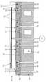
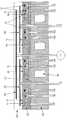
도 3은 열적 플레이트 (123) 를 갖는 가열 플레이트의 일 실시예를 포함하는 기판 지지 어셈블리 (120) 를 나타낸다. 열적 플레이트 (123) 는 폴리머 재료, 무기물 재료, 실리콘 산화물과 같은 세라믹, 알루미나, 이트리아, 알루미늄 질화물 또는 다른 적절한 재료로 만들어진 하나 이상의 층들로 구성될 수 있다. 기판 지지 어셈블리 (120) 는 DC 전압을 클램핑 전극에 가함으로써, 기판을 어셈블리 (120) 의 노출된 상부 표면으로 정전기적으로 클램핑하도록 열적 플레이트 (123) 에 합체되거나 부착된 적어도 하나의 ESC (electrostatic clamping) 전극 (124) (예를 들면, 단극성 또는 쌍극성) 을 포함하는 유전체 층을 더 포함하며, 냉각제 흐름을 위한 채널 (126) 들을 포함하는 냉각 플레이트 (105) 는 열적 플레이트 (123) 의 하부 표면에 부착된다. 냉각 플레이트는 예를 들어 -20°C 에서 +80°C의 일정한 온도로 유지될 수 있다. 또한 기판 지지 어셈블리 (120) 는 열적 플레이트 (123) 에 포함된 열적 존들 (T1, T2, T3, T4) 을 포함하며, 각 열적 존은 공통 라인 (107) , 양 전압 라인 (128) 및 음 전압 라인 (109) 에 연결된 단일 열전기 펠티에 디바이스 또는 펠티에 엘리먼트들 (P1, P2, P3, P4) 의 모듈을 포함한다. 다이오드들 (121) 은 라인 (128, 109) 과 펠티에 디바이스 (P1, P2, P3, P4) 의 사이에 제공된다. 정전기적 클램핑 전극 (124) 은 클램핑 전압 공급 라인 (111) 에 연결된다.FIG. 3 shows a
도 3에서 보듯이, 각각의 평면형 열적 존들 (T1, T2, T3, T4) 은 양 전압 라인 (128), 음 전압 라인 (109) 및 공통 라인 (107) 에 연결된다. 어떤 두 평면형 열적 존 (T1, T2) 도 동일한 쌍의 라인들 (128 / 109 및 107) 을 공유하지 않는다. 적절한 전기적 스위칭 장치들을 통해, 양 전압 라인 (128) 또는 음 전압 라인 (109) 및 공통 라인들 (107) 중 하나를 전력 공급부 (미도시) 에 연결할 수 있으며, 이로써 이 라인들의 쌍과 연결된 평면형 열적 존만이 전력을 공급 받는다. 각 평면형 열적 존의 시간 평균적 가열 전력은 시간 영역 다중화 (time-domain multiplexing) 를 통해 개별적으로 조절될 수 있다. 각 평면형 열적 존 (T1, T2, T3, T4) 과 양 전압 라인 또는 음 전압 라인 사이에 연결된 다이오드 (121) 는 평면형 열적 존으로부터 비활성화 전압 라인으로 전류 흐름을 허용하지 않는다. 다이오드들 (121) 은 열적 플레이트 또는 임의의 적절한 장소에 물리적으로 위치될 수 있다. 양 전압 라인 또는 음 전압 라인을 활성화하는 것을 통해, 펠티에 디바이스들의 반대측이 냉각 플레이트 (105) 에 의해 냉각 또는 가열되는 동안 평면형 열적 존의 상부 표면의 가열 또는 냉각이 실행될 수 있다.3, each of the planar thermal zones T1, T2, T3, and T4 is connected to a
공통 라인들 (107) , 양 전압 라인들 (128) 및 음 전압 라인들 (109) 을 포함하는 전기적인 구성요소들은 열적 플레이트 (123) 내에서 전기 절연성 재료를 통해 서로 분리된 다양한 평면들 내에 임의의 적합한 순서로 배열될 수 있다. 상기 평면들 사이의 전기적인 접속들은 적합하게 배열되고 수직하게 연장된 비아들 (vias) 을 통해 이루어 질 수 있다. 바람직하게는, 평면형 열적 존들 (T1, T2 등) 은 기판 지지 어셈블리 상부 표면과 가장 가깝게 배열된다. 버스 라인들 (125) 은 라인들 (128, 109) 을 펠티에 디바이스들 (P1-P4) 에 연결한다.Electrical components including
도 4에서 보듯이, 기판 지지 어셈블리 (120) 는 하나 이상의 추가적인 가열기들 (122) (이하, 주 가열기로 지칭됨) 을 포함할 수 있다. 바람직하게는, 주 가열기들 (122) 은 개별적으로 제어되는 고전력 (high-power) 가열기이다. 각각의 주 가열기들의 전력은 100 과 10000W 사이이며, 바람직하게는 500 과 2000W 사이이다. 이 전력은 주 가열기 공급/복귀 라인 (113) 들을 통해 전달될 수있다. 도 4에서는 오직 두 개의 주 가열기만이 도시되지만, 주 가열기들은 예를 들어 직사각형의 그리드, 동심 환형 존들, 방사상 존 또는 환형 존들과 방사상 존들의 조합과 같은 공간적인 배열로 배열된 3개 이상의 저항 가열기들을 포함할 수 있다. 주 가열기들 (122) 은 평균 온도를 변경하거나, 방사상의 온도 프로파일을 튜닝하거나, 기판상의 단계적인 온도 제어를 위해서 사용될 수 있다. 도 4에 도시된 바와 같이, 주 가열기들 (122) 은 열적 플레이트 (123) 의 평면형 열적 존들 (101) 아래에 위치되었지만, 도 5에 도시된 바와 같이 주 가열기들은 열적 플레이트 (123) 위에 위치될 수 있다.As shown in FIG. 4, the
도 3 내지 5에 도시된 바와 같이, 열적 플레이트 (123) 는: 녹색 시트들 내로 세라믹 분말, 바인더 및 액체의 혼합물을 압축하는 단계; 상기 시트들을 건조하는 단계; 상기 시트들 내에 구멍을 뚫어 상기 녹색 시트들 내에 비아들 (vias) 을 형성하는 단계; 전도성 분말 (예를 들어, W, WC, SiC 또는 MoSi2) 의 슬러리를 스크린 프린팅하거나, 사전절단 금속박 (precut metal foil) 을 압축하거나, 전도성 분말의 슬러리를 분사하거나 임의의 다른 적절한 기술을 통하여 상기 녹색시트 상에 도전체 라인들을 형성하는 단계; 상기 시트들을 정렬하는 단계; 상기 열적 플레이트를 형성하도록 접착제로써 상기 녹색시트들을 본딩하거나 상기 시트들을 함께 소결시키는 단계; 전도성 분말의 슬러리로 비아들을 충진하는 단계; 펠티에 디바이스가 도전체 라인 (107, 128, 109) 에 연결되고, 다른 평면형 열적 존에 있는 어떤 두 펠티에 디바이스도 동일한 라인 (128/109) 쌍 및 라인 (107) 을 공유하지 않도록, 상기 열적 플레이트 상에 펠티에 디바이스 (P1, P2, P3, P4) 및 다이오드 (121) 를 본딩하는 단계; 를 포함하는 예시적인 방법을 통해 제조될 수 있다. 각각의 시트들은 두께가 약 0.3 mm 일 수 있다.As shown in Figures 3-5, the
또한 도 3 내지 5에 도시된 바와 같은, 열적 플레이트 (123) 는: (a) 유리섬유 복합재 플레이트 또는 전기 절연성 폴리머 막 (예를 들어, 폴리이미드 (polyimide)) 에 의해 피복된 금속 플레이트 상에 금속 시트 (예를 들어, 알루미늄, Inconel® 또는 구리 박막) 를 본딩 (예를 들어, 가열 압축, 접착제로 접착) 하는 단계; (b) 상기 금속 시트의 표면에 패터닝된 레지스트 막을 도포하는 단계로서, 상기 패터닝된 레지스트 막 내의 개구들이 공통 라인들의 그룹의 형상들 및 위치들을 규정하는 상기 레지스트 막을 도포하는 단계; (c) 상기 패터닝된 레지스트 막 내의 개구들을 통해 노출된 금속 시트의 부분들을 화학적으로 에칭 (etching) 함으로써 공통 라인들의 그룹을 형성하는 단계; (d) (적절한 용매에서 용해 또는 건식 에칭에 의해) 레지스트 막을 제거하는 단계; (e) 금속 시트 상에 전기 절연성 폴리머 막을 도포하는 단계; (f) 선택적으로 일회 이상 (b)~(e) 단계들을 반복하는 단계; (g) 금속 시트 (들) 및 전기 절연성 폴리머 막 (들) 을 통해 구멍들을 뚫고 전도성 분말의 슬러리로 상기 구멍들을 충진하거나, 금속 도금으로써 비아들 (vias) 을 형성하는 단계; (h) 상이한 평면형 열적 존들 내의 어떠한 2 개의 펠티에 디바이스들도 동일한 양 전압 라인 및 음 전압 라인의 쌍과 공통 라인을 공유하지 않으면서 각 평면형 열적 존 내의 펠티에 디바이스들은 양 전압 라인 및 음 전압 라인의 쌍 및 하나의 공통 라인에 연결되도록, 또 다른 전기 절연성 폴리머의 노출된 표면 상에 펠티에 디바이스들과 다이오드들을 본딩하고, 선택적으로 양 전압 라인들 및 음 전압 라인들의 그룹을 형성하며, 상기 시트들을 함께 부착하는 단계;를 포함하는 또 다른 방법으로 제조될 수 있다.3 to 5, the thermal plate 123 may be formed by: (a) providing a metal plate on a metal plate coated with a glass fiber composite plate or an electrically insulating polymer film (e.g., polyimide) a sheet (e.g., aluminum, Inconel®, or the copper foil), the step of bonding (for example, heat compression, bonding by an adhesive); (b) applying a patterned resist film to the surface of the metal sheet, wherein the openings in the patterned resist film define the shapes and locations of the group of common lines; (c) chemically etching portions of the exposed metal sheet through openings in the patterned resist film to form a group of common lines; (d) removing the resist film (by dissolution or dry etching in a suitable solvent); (e) applying an electrically insulating polymer film on the metal sheet; (f) optionally repeating steps (b) - (e) one or more times; (g) punching holes through the metal sheet (s) and the electrically insulating polymer membrane (s) and filling the pores with a slurry of conductive powder, or forming vias by metal plating; (h) any two Peltier devices in different planar thermal zones do not share a common line with pairs of the same positive voltage line and negative voltage line, and Peltier devices in each planar thermal zone are connected to a pair of positive and negative voltage lines And bonding the Peltier devices and diodes on an exposed surface of another electrically insulating polymer to form a group of positive voltage lines and negative voltage lines to be connected to one common line, The method comprising the steps of:
평면형 열적 존 (T1, T2, T3, T4) 에 전력을 공급하면, 직류 전류가 평면형 열적 존의 펠티에 디바이스 (들) 를 통해 열적 존의 가열 또는 냉각을 야기하기 위해 목표된 방향으로 향한다. 이로써 직류 전류의 방향을 선택함으로써, 평면형 열적 존은 기판 지지 어셈블리 상에 지지된 반도체 기판의 수직으로 배열된 부분을 국부적으로 가열 또는 냉각시킬 수 있다.When power is applied to the planar thermal zones T1, T2, T3, T4, the direct current is directed in the desired direction to cause heating or cooling of the thermal zone through the Peltier device (s) in the planar thermal zone. By thus selecting the direction of the direct current, the planar thermal zone can locally heat or cool vertically aligned portions of the semiconductor substrate supported on the substrate support assembly.
기판 지지 어셈블리의 제조에서의 사용을 위한 적절한 절연 재료 및 전도성 재료의 예는, 본 명세서에서 그 개시가 참조로서 인용되는, 공동으로 양도된 미국 특허 번호 6,483,690 에 개시된다.Examples of suitable insulating and conductive materials for use in the manufacture of substrate support assemblies are disclosed in commonly assigned U. S. Patent No. 6,483, 690, the disclosure of which is incorporated herein by reference.
가열 플레이트, 가열 플레이트 제조 방법 및 가열 플레이트를 포함하는 기판 지지 어셈블리가 이것의 특정 실시예를 참조하여 상세히 설명되었지만, 첨부된 청구항의 범위로부터 벗어남 없이, 다양한 수정 및 변형이 이루어질 수 있고, 균등 사항이 채용될 수 있다는 것은 본 기술분야의 당업자에게 명백할 것이다.Although a substrate support assembly including a heating plate, a method of manufacturing a heating plate, and a heating plate has been described in detail with reference to specific embodiments thereof, various modifications and variations can be made without departing from the scope of the appended claims, It will be apparent to those skilled in the art that the present invention can be employed.
Claims (17)
Translated fromKorean상기 기판 지지부는,
제 1 열적 존 (thermal zone), 제 2 열적 존, 제 3 열적 존 및 제 4 열적 존을 포함하는 열적 존들로서, 상기 열적 존들 각각은 하나 이상의 열적 엘리먼트들을 포함하고, 상기 기판 지지부의 상부 표면 상의 온도 프로파일을 튜닝하도록 (tune) 동작 가능한, 상기 열적 존들;
제 1 전기 전도성 양 전압 라인 및 제 2 전기 전도성 양 전압 라인을 포함하는 양 전압 라인들;
제 1 전기 전도성 음 전압 라인 및 제 2 전기 전도성 음 전압 라인을 포함하는 음 전압 라인들;
제 1 전기 전도성 공통 라인 및 제 2 전기 전도성 공통 라인을 포함하는 공통 라인들;
제 1 다이오드, 제 2 다이오드, 제 3 다이오드, 제 4 다이오드, 제 5 다이오드, 제 6 다이오드, 제 7 다이오드 및 제 8 다이오드를 포함하고,
상기 제 1 다이오드의 양극은 상기 제 1 양 전압 라인에 연결되고 상기 제 1 다이오드의 음극은 상기 제 1 열적 존에 연결되며;
상기 제 2 다이오드의 양극은 상기 제 1 열적 존에 연결되고 상기 제 2 다이오드의 음극은 상기 제 1 음 전압 라인에 연결되며;
상기 제 3 다이오드의 양극은 상기 제 1 양 전압 라인에 연결되고 상기 제 3 다이오드의 음극은 상기 제 2 열적 존에 연결되며;
상기 제 4 다이오드의 양극은 상기 제 2 열적 존에 연결되고 상기 제 4 다이오드의 음극은 상기 제 1 음 전압 라인에 연결되며;
상기 제 5 다이오드의 양극은 상기 제 2 양 전압 라인에 연결되고 상기 제 5 다이오드의 음극은 상기 제 3 열적 존에 연결되며;
상기 제 6 다이오드의 양극은 상기 제 3 열적 존에 연결되고 상기 제 6 다이오드의 음극은 상기 제 2 음 전압 라인에 연결되며;
상기 제 7 다이오드의 양극은 상기 제 2 양 전압 라인에 연결되고 상기 제 7 다이오드의 음극은 상기 제 4 열적 존에 연결되며;
상기 제 8 다이오드의 양극은 상기 제 4 열적 존에 연결되고 상기 제 8 다이오드의 음극은 상기 제 2 음 전압 라인에 연결되며;
상기 제 1 공통 라인은 상기 제 1 열적 존 및 상기 제 3 열적 존 양자에 연결되며;
상기 제 2 공통 라인은 상기 제 2 열적 존 및 상기 제 4 열적 존 양자에 연결되는, 반도체 처리 장치 내의 반도체 기판의 지지를 위한 기판 지지부.A substrate supporting portion for supporting a semiconductor substrate in a semiconductor processing apparatus,
The substrate-
A thermal zone comprising a first thermal zone, a second thermal zone, a third thermal zone and a fourth thermal zone, wherein each of the thermal zones comprises one or more thermal elements, The thermal zones operable to tune a temperature profile;
Positive voltage lines including a first electrically conductive positive voltage line and a second electrically conductive positive voltage line;
Negative voltage lines including a first electrically conductive negative voltage line and a second electrically conductive negative voltage line;
Common lines comprising a first electrically conductive common line and a second electrically conductive common line;
A first diode, a second diode, a third diode, a fourth diode, a fifth diode, a sixth diode, a seventh diode and an eighth diode,
The anode of the first diode being connected to the first positive voltage line and the cathode of the first diode being connected to the first thermal zone;
The anode of the second diode being connected to the first thermal zone and the cathode of the second diode being connected to the first negative voltage line;
The anode of the third diode being connected to the first positive voltage line and the cathode of the third diode being connected to the second thermal zone;
The anode of the fourth diode being connected to the second thermal zone and the cathode of the fourth diode being connected to the first negative voltage line;
The anode of the fifth diode being connected to the second positive voltage line and the cathode of the fifth diode being connected to the third thermal zone;
The anode of the sixth diode is connected to the third thermal zone and the cathode of the sixth diode is connected to the second negative voltage line;
The anode of the seventh diode is connected to the second positive voltage line and the cathode of the seventh diode is connected to the fourth thermal zone;
The anode of the eighth diode is connected to the fourth thermal zone and the cathode of the eighth diode is connected to the second negative voltage line;
The first common line is connected to both the first thermal zone and the third thermal zone;
And the second common line is connected to both the second thermal zone and the fourth thermal zone.
상기 열적 엘리먼트들은 어떠한 저항성 가열기 엘리먼트들도 포함하지 않는, 반도체 처리 장치 내의 반도체 기판의 지지를 위한 기판 지지부.The method according to claim 1,
Wherein the thermal elements do not include any resistive heater elements.
(a) 상기 열적 존들은 전기 절연성 플레이트의 상부 부분에 위치하며; 상기 양 전압 라인 및 상기 음 전압 라인은 상기 열적 존들의 하측에 배치되고, 상기 전기 절연성 플레이트에 수직으로 연장된 비아들 (vias) 에 의해 상기 다이오드들에 전기적으로 연결되며; 상기 공통 라인들은 상기 양 전압 라인 및 상기 음 전압 라인의 하측에 있고, 상기 전기 절연성 플레이트에 수직으로 연장된 비아들에 의해 상기 열적 존들에 전기적으로 연결되는, 반도체 처리 장치 내의 반도체 기판의 지지를 위한 기판 지지부.The method according to claim 1,
(a) the thermal zones are located at an upper portion of the electrically insulating plate; Wherein the positive voltage line and the negative voltage line are disposed below the thermal zones and are electrically connected to the diodes by vias extending perpendicularly to the insulating plate; Wherein the common lines are below the positive voltage line and the negative voltage line and are electrically connected to the thermal zones by vias extending perpendicularly to the electrically insulating plate. A substrate support.
상기 열적 엘리먼트들은 열전기 엘리먼트들을 포함하는, 반도체 처리 장치 내의 반도체 기판의 지지를 위한 기판 지지부.The method according to claim 1,
Wherein the thermal elements comprise thermoelectric elements. ≪ Desc / Clms Page number 17 >
상기 열적 존들은,
(a) 열적 존 각각이 0.1 내지 1 ㎠이거나,
(b) 열적 존 각각이 1 내지 3 ㎠이거나,
(c) 열적 존 각각이 3 내지 15 ㎠ 이거나,
(d) 열적 존 각각이 15 내지 100 ㎠이도록,
크기가 정해지는 (sized), 반도체 처리 장치 내의 반도체 기판의 지지를 위한 기판 지지부.The method according to claim 1,
The thermal zones include,
(a) each of the thermal zones is between 0.1 and 1 cm2,
(b) each thermal zone is between 1 and 3 cm2,
(c) each of the thermal zones is between 3 and 15 cm2,
(d) each thermal zone is between 15 and 100 cm2,
A substrate support for supporting a semiconductor substrate in a semiconductor processing apparatus, the substrate support being sized.
상기 기판 지지부는 16 내지 400 개의 열적 존들을 포함하는, 반도체 처리 장치 내의 반도체 기판의 지지를 위한 기판 지지부.The method according to claim 1,
Wherein the substrate support comprises between 16 and 400 thermal zones.
상기 전기 절연성 플레이트는 폴리머 재료, 세라믹 재료, 유리섬유 복합재 또는 이들의 조합의 하나 이상의 층들을 포함하는, 반도체 처리 장치 내의 반도체 기판의 지지를 위한 기판 지지부.The method of claim 3,
Wherein the electrically insulative plate comprises one or more layers of a polymer material, a ceramic material, a glass fiber composite, or a combination thereof.
상기 양 전압 라인들의 총 개수는 상기 열적 존들의 총 개수의 절반의 이하이거나, 상기 공통 라인들의 총 개수는 상기 열적 존들의 총 개수의 절반 이하인, 반도체 처리 장치 내의 반도체 기판의 지지를 위한 기판 지지부.The method according to claim 1,
Wherein the total number of positive voltage lines is less than or equal to half of the total number of thermal zones, or the total number of common lines is less than or equal to half the total number of thermal zones.
상기 열적 존들의 총 면적이 열적 플레이트의 상부 표면의 50 % 내지 100 %인, 반도체 처리 장치 내의 반도체 기판의 지지를 위한 기판 지지부.The method according to claim 1,
Wherein the total area of the thermal zones is 50% to 100% of the upper surface of the thermal plate.
상기 열적 존들은 직사각형의 그리드, 육각형의 그리드 또는 극좌표 어레이 (polar array) 로 배열되고; 상기 열적 존들은 최소 1 밀리미터의 폭 및 최대 10 밀리미터의 폭을 갖는 갭들 (gap) 에 의해서 서로 분리되는, 반도체 처리 장치 내의 반도체 기판의 지지를 위한 기판 지지부.The method according to claim 1,
Wherein the thermal zones are arranged in a rectangular grid, a hexagonal grid or a polar array; Wherein the thermal zones are separated from each other by gaps having a width of at least 1 millimeter and a width of at most 10 millimeters.
상기 정전척을 지지하는 제 1 항에 기재된 상기 기판 지지부의 상부 측; 및
상기 기판 지지부의 하부 측에 부착되는 온도 제어형 베이스 플레이트를 포함하는, 기판 지지 어셈블리.An electrostatic chuck (ESC) comprising at least one electrostatic clamping electrode configured to electrostatically clamp a semiconductor substrate on a substrate support assembly;
An upper side of the substrate supporting unit according to claim 1 supporting the electrostatic chuck; And
And a temperature-controlled base plate attached to a lower side of the substrate support.
기판 지지 플레이트 위 또는 아래에 배치된 적어도 하나의 주 (primary) 가열기 층을 더 포함하며,
상기 주 가열기 층은 상기 열적 존들과 전기적으로 절연되며,
상기 주 가열기 층은 상기 기판 지지부의 평균 온도 제어를 제공하는 적어도 하나의 저항 가열기를 포함하는, 기판 지지 어셈블리.12. The method of claim 11,
Further comprising at least one primary heater layer disposed above or below the substrate support plate,
The primary heater layer is electrically insulated from the thermal zones,
Wherein the primary heater layer comprises at least one resistance heater that provides an average temperature control of the substrate support.
세라믹 분말, 바인더 및 액체의 혼합물을 시트들로 압축하는 단계;
상기 시트들을 건조하는 단계;
상기 시트들 내에 구멍들을 뚫어 상기 시트들 내에 비아들 (vias) 을 형성하는 단계;
상기 시트들 상에 상기 양 전압 라인들, 상기 음 전압 라인들 및 상기 공통 라인들을 형성하는 단계;
상기 시트들을 정렬하는 단계;
상기 기판 지지부를 형성하도록 접착제로서 상기 시트들을 본딩하거나 소결시키는 단계;
전도성 분말의 슬러리로 상기 비아들을 충진 (filling) 하는 단계; 및
2개의 열적 존들이 동일한 공통 라인 및 양 전압 라인들과 음 전압 라인들의 쌍을 공유하지 않도록, 상기 열적 존 각각이 상기 양 전압 라인들 및 상기 음 전압 라인들의 쌍과 상기 하나의 공통 라인에 연결되도록, 상기 기판 지지부 상에 상기 열적 엘리먼트들을 본딩하는 단계를 포함하는, 기판 지지부를 제조하는 방법.A method of manufacturing the substrate support of claim 1,
Compressing a mixture of ceramic powder, binder and liquid into sheets;
Drying the sheets;
Piercing holes in the sheets to form vias in the sheets;
Forming the positive voltage lines, the negative voltage lines and the common lines on the sheets;
Aligning the sheets;
Bonding or sintering the sheets as an adhesive to form the substrate support;
Filling the vias with a slurry of conductive powder; And
Such that each of the thermal zones is coupled to the pair of positive voltage lines and to the common line, such that the two thermal zones do not share the same common line and positive voltage line pairs with positive voltage lines. And bonding the thermal elements on the substrate support.
상기 양 전압 라인들, 상기 음 전압 라인들 및 상기 공통 라인들은, 전도성 분말의 슬러리를 스크린 프린팅하거나, 사전절단 금속박 (precut metal foil) 을 압축 (pressing) 하거나, 전도성 분말의 슬러리를 분사함으로써 형성되는, 기판 지지부를 제조하는 방법.14. The method of claim 13,
The positive voltage lines, the negative voltage lines and the common lines are formed by screen printing a slurry of the conductive powder, pressing a precut metal foil, or spraying a slurry of the conductive powder ≪ / RTI >
(a) 유리섬유 복합재 플레이트 또는 전기 절연성 폴리머 막에 의해 피복된 금속 플레이트 상에 금속 시트를 본딩하는 단계;
(b) 상기 금속 시트의 표면에 패터닝된 (patterned) 레지스트 막을 도포하는 단계로서, 상기 패터닝된 레지스트 막 내의 개구들이 양 전압 라인들, 음 전압 라인들 및 공통 라인들 중 적어도 하나에 대응하는 도전체 라인들의 그룹의 형상들 및 위치들을 규정하는, 상기 레지스트 막을 도포하는 단계;
(c) 상기 패터닝된 레지스트 막 내의 상기 개구들을 통해 노출된 상기 금속 시트의 부분들을 화학적으로 에칭함으로써 상기 도전체 라인들의 그룹을 형성하는 단계;
(d) 상기 레지스트 막을 제거하는 단계;
(e) 상기 금속 시트 상에 전기 절연성 폴리머 막을 도포하는 단계;
(f) 선택 가능하게 1회 이상 단계들 (b) 내지 (e) 를 반복하는 단계;
(g) 상기 금속 시트 및 상기 전기 절연성 폴리머 막을 통해 구멍들을 뚫고, 금속, 전도성 분말의 슬러리, 전도성 접착제 또는 전도성 폴리머 중 적어도 하나로 상기 구멍들을 충진함으로써 비아들을 형성하는 단계;
(h) 열적 존 각각 내의 하나 이상의 열적 엘리먼트들이 양 전압 라인과 음 전압 라인의 쌍 및 하나의 공통 라인에 연결되고, 상이한 열적 존들 내의 2 개의 열적 엘리먼트들이 동일한 공통 라인 및 양 전압 라인과 음 전압 라인의 쌍을 공유하지 않도록 상기 기판 지지부를 형성하기 위해서 상기 열적 엘리먼트들을 하나 이상의 전기 절연성 폴리머 막들에 본딩하고 상기 폴리머 막들을 어셈블링하는 단계를 포함하는, 기판 지지부를 제조하는 방법.A method of manufacturing the substrate support of claim 1,
(a) bonding a metal sheet onto a metal plate coated with a glass fiber composite material plate or an electrically insulating polymer film;
(b) applying a patterned resist film to the surface of the metal sheet, wherein the openings in the patterned resist film are electrically connected to at least one of positive voltage lines, negative voltage lines and common lines Applying the resist film to define shapes and locations of groups of lines;
(c) chemically etching portions of the metal sheet exposed through the openings in the patterned resist film to form a group of the conductor lines;
(d) removing the resist film;
(e) applying an electrically insulating polymer film on the metal sheet;
(f) optionally repeating steps (b) through (e) one or more times;
(g) forming vias by drilling holes through the metal sheet and the electrically insulating polymer membrane and filling the holes with at least one of a metal, a slurry of conductive powder, a conductive adhesive, or a conductive polymer;
(h) one or more thermal elements in each of the thermal zones are connected to a pair of positive voltage lines and negative voltage lines and one common line, and two thermal elements in different thermal zones are connected to the same common line, Bonding the thermal elements to one or more electrically insulating polymeric films and assembling the polymeric films to form the substrate support so as not to share a pair of polymeric films.
(a) 상기 처리 챔버 내로 상기 반도체 기판을 로딩하고 상기 기판 지지 어셈블리 상에 상기 반도체 기판을 위치시키는 단계;
(b) 임계 치수 (CD: critical dimension) 균일성에 영향을 미치는 처리 조건들을 보상하는 온도 프로파일을 결정하는 단계;
(c) 상기 기판 지지 어셈블리를 사용하여 상기 온도 프로파일에 부합하도록 상기 반도체 기판을 가열하는 단계;
(d) 상기 열적 존들의 독립적으로 제어되는 가열 또는 냉각에 의해서 상기 온도 프로파일을 제어하는 동안 플라즈마를 점화하고, 상기 반도체 기판을 처리하는 단계;
(e) 상기 반도체 기판을 상기 처리 챔버로부터 언로딩 (unloading) 하고, 상이한 반도체 기판에 대해서 상기 단계들 (a) 내지 (e) 를 반복하는 단계를 포함하는, 반도체 기판들을 플라즈마 처리하는 방법.13. A method of plasma processing semiconductor substrates in a plasma processing chamber comprising the substrate support assembly of claim 11,
(a) loading the semiconductor substrate into the processing chamber and positioning the semiconductor substrate on the substrate support assembly;
(b) determining a temperature profile that compensates for processing conditions affecting critical dimension (CD) uniformity;
(c) heating the semiconductor substrate to conform to the temperature profile using the substrate support assembly;
(d) igniting the plasma while controlling the temperature profile by independently controlled heating or cooling of the thermal zones, and processing the semiconductor substrate;
(e) unloading the semiconductor substrate from the processing chamber and repeating the steps (a) - (e) for a different semiconductor substrate.
상기 주 가열기 층이 2 개 이상의 가열기들을 포함하는, 기판 지지 어셈블리.13. The method of claim 12,
Wherein the primary heater layer comprises two or more heaters.
Applications Claiming Priority (3)
| Application Number | Priority Date | Filing Date | Title |
|---|---|---|---|
| US13/238,396US8461674B2 (en) | 2011-09-21 | 2011-09-21 | Thermal plate with planar thermal zones for semiconductor processing |
| US13/238,396 | 2011-09-21 | ||
| PCT/IB2012/054903WO2013042027A2 (en) | 2011-09-21 | 2012-09-17 | Thermal plate with planar thermal zones for semiconductor processing |
Related Parent Applications (1)
| Application Number | Title | Priority Date | Filing Date |
|---|---|---|---|
| KR1020147010282ADivisionKR101643828B1 (en) | 2011-09-21 | 2012-09-17 | Thermal plate with planar thermal zones for semiconductor processing |
Publications (2)
| Publication Number | Publication Date |
|---|---|
| KR20160091456A KR20160091456A (en) | 2016-08-02 |
| KR101822318B1true KR101822318B1 (en) | 2018-01-25 |
Family
ID=47881062
Family Applications (2)
| Application Number | Title | Priority Date | Filing Date |
|---|---|---|---|
| KR1020167020061AActiveKR101822318B1 (en) | 2011-09-21 | 2012-09-17 | Thermal plate with planar thermal zones for semiconductor processing |
| KR1020147010282AActiveKR101643828B1 (en) | 2011-09-21 | 2012-09-17 | Thermal plate with planar thermal zones for semiconductor processing |
Family Applications After (1)
| Application Number | Title | Priority Date | Filing Date |
|---|---|---|---|
| KR1020147010282AActiveKR101643828B1 (en) | 2011-09-21 | 2012-09-17 | Thermal plate with planar thermal zones for semiconductor processing |
Country Status (7)
| Country | Link |
|---|---|
| US (2) | US8461674B2 (en) |
| JP (1) | JP6144263B2 (en) |
| KR (2) | KR101822318B1 (en) |
| CN (1) | CN104471682B (en) |
| SG (3) | SG11201400623XA (en) |
| TW (2) | TWI563592B (en) |
| WO (1) | WO2013042027A2 (en) |
Families Citing this family (56)
| Publication number | Priority date | Publication date | Assignee | Title |
|---|---|---|---|---|
| SG180882A1 (en) | 2009-12-15 | 2012-07-30 | Lam Res Corp | Adjusting substrate temperature to improve cd uniformity |
| US8546732B2 (en) | 2010-11-10 | 2013-10-01 | Lam Research Corporation | Heating plate with planar heater zones for semiconductor processing |
| US9307578B2 (en) | 2011-08-17 | 2016-04-05 | Lam Research Corporation | System and method for monitoring temperatures of and controlling multiplexed heater array |
| US10388493B2 (en) | 2011-09-16 | 2019-08-20 | Lam Research Corporation | Component of a substrate support assembly producing localized magnetic fields |
| US9324589B2 (en)* | 2012-02-28 | 2016-04-26 | Lam Research Corporation | Multiplexed heater array using AC drive for semiconductor processing |
| US9157730B2 (en) | 2012-10-26 | 2015-10-13 | Applied Materials, Inc. | PECVD process |
| WO2014164910A1 (en) | 2013-03-12 | 2014-10-09 | Applied Materials, Inc. | Multi zone heating and cooling esc for plasma process chamber |
| US10332772B2 (en) | 2013-03-13 | 2019-06-25 | Applied Materials, Inc. | Multi-zone heated ESC with independent edge zones |
| US20140356985A1 (en) | 2013-06-03 | 2014-12-04 | Lam Research Corporation | Temperature controlled substrate support assembly |
| TW201518538A (en) | 2013-11-11 | 2015-05-16 | Applied Materials Inc | Pixelated cooling, temperature controlled substrate support assembly |
| US10460968B2 (en) | 2013-12-02 | 2019-10-29 | Applied Materials, Inc. | Electrostatic chuck with variable pixelated magnetic field |
| US10217615B2 (en)* | 2013-12-16 | 2019-02-26 | Lam Research Corporation | Plasma processing apparatus and component thereof including an optical fiber for determining a temperature thereof |
| US9716022B2 (en)* | 2013-12-17 | 2017-07-25 | Lam Research Corporation | Method of determining thermal stability of a substrate support assembly |
| US9622375B2 (en) | 2013-12-31 | 2017-04-11 | Applied Materials, Inc. | Electrostatic chuck with external flow adjustments for improved temperature distribution |
| US9520315B2 (en) | 2013-12-31 | 2016-12-13 | Applied Materials, Inc. | Electrostatic chuck with internal flow adjustments for improved temperature distribution |
| US20150221481A1 (en)* | 2014-01-31 | 2015-08-06 | Michael D. Willwerth | Electrostatic chuck with magnetic cathode liner for critical dimension (cd) tuning |
| US9435692B2 (en) | 2014-02-05 | 2016-09-06 | Lam Research Corporation | Calculating power input to an array of thermal control elements to achieve a two-dimensional temperature output |
| US11158526B2 (en)* | 2014-02-07 | 2021-10-26 | Applied Materials, Inc. | Temperature controlled substrate support assembly |
| US9589853B2 (en) | 2014-02-28 | 2017-03-07 | Lam Research Corporation | Method of planarizing an upper surface of a semiconductor substrate in a plasma etch chamber |
| US9472410B2 (en) | 2014-03-05 | 2016-10-18 | Applied Materials, Inc. | Pixelated capacitance controlled ESC |
| US9580360B2 (en) | 2014-04-07 | 2017-02-28 | Lam Research Corporation | Monolithic ceramic component of gas delivery system and method of making and use thereof |
| US9543171B2 (en) | 2014-06-17 | 2017-01-10 | Lam Research Corporation | Auto-correction of malfunctioning thermal control element in a temperature control plate of a semiconductor substrate support assembly that includes deactivating the malfunctioning thermal control element and modifying a power level of at least one functioning thermal control element |
| WO2016003633A1 (en) | 2014-07-02 | 2016-01-07 | Applied Materials, Inc | Apparatus, systems, and methods for temperature control of substrates using embedded fiber optics and epoxy optical diffusers |
| KR101758087B1 (en) | 2014-07-23 | 2017-07-14 | 어플라이드 머티어리얼스, 인코포레이티드 | Tunable temperature controlled substrate support assembly |
| US9872341B2 (en) | 2014-11-26 | 2018-01-16 | Applied Materials, Inc. | Consolidated filter arrangement for devices in an RF environment |
| JP6530220B2 (en)* | 2015-03-30 | 2019-06-12 | 日本特殊陶業株式会社 | Ceramic heater and control method thereof, and electrostatic chuck and control method thereof |
| US10453775B1 (en)* | 2015-06-10 | 2019-10-22 | SA Photonics, Inc. | Distributed thermoelectric cooling system |
| US10381248B2 (en) | 2015-06-22 | 2019-08-13 | Lam Research Corporation | Auto-correction of electrostatic chuck temperature non-uniformity |
| US9779974B2 (en) | 2015-06-22 | 2017-10-03 | Lam Research Corporation | System and method for reducing temperature transition in an electrostatic chuck |
| US10386821B2 (en) | 2015-06-22 | 2019-08-20 | Lam Research Corporation | Systems and methods for calibrating scalar field contribution values for a limited number of sensors including a temperature value of an electrostatic chuck and estimating temperature distribution profiles based on calibrated values |
| US10763142B2 (en) | 2015-06-22 | 2020-09-01 | Lam Research Corporation | System and method for determining field non-uniformities of a wafer processing chamber using a wafer processing parameter |
| US9864361B2 (en) | 2015-06-22 | 2018-01-09 | Lam Research Corporation | Flexible temperature compensation systems and methods for substrate processing systems |
| JP6655310B2 (en)* | 2015-07-09 | 2020-02-26 | 株式会社日立ハイテクノロジーズ | Plasma processing equipment |
| US9684754B2 (en)* | 2015-10-02 | 2017-06-20 | Arm Limited | Standard cell architecture layout |
| US9826574B2 (en)* | 2015-10-28 | 2017-11-21 | Watlow Electric Manufacturing Company | Integrated heater and sensor system |
| US9812342B2 (en)* | 2015-12-08 | 2017-11-07 | Watlow Electric Manufacturing Company | Reduced wire count heater array block |
| US10845375B2 (en)* | 2016-02-19 | 2020-11-24 | Agjunction Llc | Thermal stabilization of inertial measurement units |
| JP6226092B2 (en)* | 2016-03-14 | 2017-11-08 | Toto株式会社 | Electrostatic chuck |
| KR102062751B1 (en)* | 2016-03-29 | 2020-01-06 | 엔지케이 인슐레이터 엘티디 | Electrostatic chuck heater |
| US10973088B2 (en) | 2016-04-18 | 2021-04-06 | Applied Materials, Inc. | Optically heated substrate support assembly with removable optical fibers |
| JP6238097B1 (en)* | 2016-07-20 | 2017-11-29 | Toto株式会社 | Electrostatic chuck |
| US10685861B2 (en) | 2016-08-26 | 2020-06-16 | Applied Materials, Inc. | Direct optical heating of substrates through optical guide |
| US20180213608A1 (en)* | 2017-01-20 | 2018-07-26 | Applied Materials, Inc. | Electrostatic chuck with radio frequency isolated heaters |
| US11276590B2 (en) | 2017-05-17 | 2022-03-15 | Applied Materials, Inc. | Multi-zone semiconductor substrate supports |
| KR102434561B1 (en)* | 2017-06-29 | 2022-08-23 | 주식회사 케이씨텍 | Apparatus and Method for processing substrate |
| KR102156365B1 (en)* | 2018-07-04 | 2020-09-15 | (주)케이에스티이 | Electrostatic chuck having heater and method of manufacturing the same |
| WO2020027993A1 (en)* | 2018-08-03 | 2020-02-06 | Applied Materials, Inc. | Multizone lamp control and individual lamp control in a lamphead |
| KR20200023988A (en) | 2018-08-27 | 2020-03-06 | 삼성전자주식회사 | Electro-static chuck and wafer etching device comprising the same |
| TW202437459A (en) | 2018-12-07 | 2024-09-16 | 美商蘭姆研究公司 | Long-life extended temperature range embedded diode design for electrostatic chuck with multiplexed heaters array |
| US11564292B2 (en) | 2019-09-27 | 2023-01-24 | Applied Materials, Inc. | Monolithic modular microwave source with integrated temperature control |
| JP7316179B2 (en)* | 2019-10-04 | 2023-07-27 | 東京エレクトロン株式会社 | SUBSTRATE SUPPORT AND PLASMA PROCESSING APPARATUS |
| JP7018978B2 (en)* | 2020-01-31 | 2022-02-14 | 株式会社日立ハイテク | Plasma processing equipment |
| JP6900139B1 (en) | 2020-12-22 | 2021-07-07 | 株式会社浅野研究所 | Thermoforming equipment and thermoforming method |
| KR102768789B1 (en) | 2021-02-04 | 2025-02-14 | 엔지케이 인슐레이터 엘티디 | Components for semiconductor manufacturing devices and their manufacturing method |
| KR102654892B1 (en)* | 2021-07-28 | 2024-04-05 | 세메스 주식회사 | Support unit, heating unit and substrate processing apparatus including the same |
| CN116403943A (en)* | 2023-04-21 | 2023-07-07 | 江苏微导纳米科技股份有限公司 | A heating plate and its manufacturing method, a semiconductor device |
Citations (3)
| Publication number | Priority date | Publication date | Assignee | Title |
|---|---|---|---|---|
| JP2002299319A (en) | 2001-03-29 | 2002-10-11 | Hitachi Kokusai Electric Inc | Substrate processing equipment |
| JP2005101237A (en) | 2003-09-24 | 2005-04-14 | Tokyo Electron Ltd | Heat treatment equipment |
| US20110143462A1 (en) | 2009-12-15 | 2011-06-16 | Lam Research Corporation | Adjusting substrate temperature to improve cd uniformity |
Family Cites Families (81)
| Publication number | Priority date | Publication date | Assignee | Title |
|---|---|---|---|---|
| US3440883A (en) | 1966-12-01 | 1969-04-29 | Monsanto Co | Electronic semiconductor thermometer |
| JPS58153387A (en)* | 1982-03-08 | 1983-09-12 | Toshiba Corp | temperature control device |
| JPS59139654A (en)* | 1984-01-13 | 1984-08-10 | Hitachi Ltd | Control circuit for temperature |
| JPS61142743A (en)* | 1984-12-15 | 1986-06-30 | Nec Corp | Equipment for manufacturing semiconductor |
| JPH01152655A (en)* | 1987-12-09 | 1989-06-15 | Fujitsu Ltd | Peltier element control circuit |
| JPH0487321A (en)* | 1990-07-31 | 1992-03-19 | Japan Synthetic Rubber Co Ltd | Holding device of object to be treated in vacuum treatment apparatus |
| US5536918A (en) | 1991-08-16 | 1996-07-16 | Tokyo Electron Sagami Kabushiki Kaisha | Heat treatment apparatus utilizing flat heating elements for treating semiconductor wafers |
| FR2682253A1 (en) | 1991-10-07 | 1993-04-09 | Commissariat Energie Atomique | HEATING SOLE FOR PROVIDING THE HEATING OF AN OBJECT PROVIDED ON ITS SURFACE AND CHEMICAL PROCESSING REACTOR PROVIDED WITH SAID SOLE. |
| US5255520A (en) | 1991-12-20 | 1993-10-26 | Refir Technologies | Advanced thermoelectric heating and cooling system |
| US5414245A (en) | 1992-08-03 | 1995-05-09 | Hewlett-Packard Corporation | Thermal-ink heater array using rectifying material |
| DE4231702C2 (en) | 1992-09-22 | 1995-05-24 | Litef Gmbh | Thermoelectric, heatable cooling chamber |
| KR100290748B1 (en) | 1993-01-29 | 2001-06-01 | 히가시 데쓰로 | Plasma processing apparatus |
| US5504471A (en) | 1993-09-16 | 1996-04-02 | Hewlett-Packard Company | Passively-multiplexed resistor array |
| US5667622A (en)* | 1995-08-25 | 1997-09-16 | Siemens Aktiengesellschaft | In-situ wafer temperature control apparatus for single wafer tools |
| JPH09213781A (en) | 1996-02-01 | 1997-08-15 | Tokyo Electron Ltd | Stage structure and processor using it |
| US6095084A (en) | 1996-02-02 | 2000-08-01 | Applied Materials, Inc. | High density plasma process chamber |
| US5740016A (en) | 1996-03-29 | 1998-04-14 | Lam Research Corporation | Solid state temperature controlled substrate holder |
| US5802856A (en) | 1996-07-31 | 1998-09-08 | Stanford University | Multizone bake/chill thermal cycling module |
| JP3526184B2 (en) | 1997-03-17 | 2004-05-10 | 大日本スクリーン製造株式会社 | Substrate processing equipment |
| JP2954908B2 (en)* | 1997-09-30 | 1999-09-27 | エスエムシー株式会社 | Substrate temperature controller |
| US6222161B1 (en) | 1998-01-12 | 2001-04-24 | Tokyo Electron Limited | Heat treatment apparatus |
| US5886866A (en) | 1998-07-06 | 1999-03-23 | Applied Materials, Inc. | Electrostatic chuck having a combination electrode structure for substrate chucking, heating and biasing |
| JP3892609B2 (en) | 1999-02-16 | 2007-03-14 | 株式会社東芝 | Hot plate and method for manufacturing semiconductor device |
| DE19907497C2 (en) | 1999-02-22 | 2003-05-28 | Steag Hamatech Ag | Device and method for heat treatment of substrates |
| US6353209B1 (en) | 1999-03-04 | 2002-03-05 | Board Of Trustees Of The Leland Stanford Junior University | Temperature processing module |
| US6523493B1 (en) | 2000-08-01 | 2003-02-25 | Tokyo Electron Limited | Ring-shaped high-density plasma source and method |
| US6175175B1 (en) | 1999-09-10 | 2001-01-16 | The University Of Chicago | Levitation pressure and friction losses in superconducting bearings |
| US6740853B1 (en) | 1999-09-29 | 2004-05-25 | Tokyo Electron Limited | Multi-zone resistance heater |
| EP1199908A4 (en) | 1999-10-22 | 2003-01-22 | Ibiden Co Ltd | Ceramic heater |
| US6271459B1 (en) | 2000-04-26 | 2001-08-07 | Wafermasters, Inc. | Heat management in wafer processing equipment using thermoelectric device |
| US6475336B1 (en) | 2000-10-06 | 2002-11-05 | Lam Research Corporation | Electrostatically clamped edge ring for plasma processing |
| US7075031B2 (en) | 2000-10-25 | 2006-07-11 | Tokyo Electron Limited | Method of and structure for controlling electrode temperature |
| AU2002240261A1 (en) | 2001-03-02 | 2002-09-19 | Tokyo Electron Limited | Method and apparatus for active temperature control of susceptors |
| US6746616B1 (en) | 2001-03-27 | 2004-06-08 | Advanced Micro Devices, Inc. | Method and apparatus for providing etch uniformity using zoned temperature control |
| US6741446B2 (en) | 2001-03-30 | 2004-05-25 | Lam Research Corporation | Vacuum plasma processor and method of operating same |
| JP3582518B2 (en) | 2001-04-18 | 2004-10-27 | 住友電気工業株式会社 | Resistance heating element circuit pattern and substrate processing apparatus using the same |
| US6847014B1 (en) | 2001-04-30 | 2005-01-25 | Lam Research Corporation | Method and apparatus for controlling the spatial temperature distribution across the surface of a workpiece support |
| JP4549022B2 (en) | 2001-04-30 | 2010-09-22 | ラム リサーチ コーポレイション | Method and apparatus for controlling spatial temperature distribution across the surface of a workpiece support |
| US6795292B2 (en) | 2001-05-15 | 2004-09-21 | Dennis Grimard | Apparatus for regulating temperature of a process kit in a semiconductor wafer-processing chamber |
| US20060191637A1 (en) | 2001-06-21 | 2006-08-31 | John Zajac | Etching Apparatus and Process with Thickness and Uniformity Control |
| JP3897563B2 (en) | 2001-10-24 | 2007-03-28 | 日本碍子株式会社 | Heating device |
| JP2003133402A (en)* | 2001-10-26 | 2003-05-09 | Hitachi High-Technologies Corp | Sample holding device |
| US6739138B2 (en) | 2001-11-26 | 2004-05-25 | Innovations Inc. | Thermoelectric modules and a heating and cooling apparatus incorporating same |
| JP4087190B2 (en)* | 2002-02-12 | 2008-05-21 | 古河電気工業株式会社 | OPTICAL DEVICE, OPTICAL DEVICE START-UP METHOD AND DRIVE METHOD, AND OPTICAL COMMUNICATION DEVICE |
| US6921724B2 (en) | 2002-04-02 | 2005-07-26 | Lam Research Corporation | Variable temperature processes for tunable electrostatic chuck |
| JP3808407B2 (en) | 2002-07-05 | 2006-08-09 | 住友大阪セメント株式会社 | Electrode built-in susceptor and manufacturing method thereof |
| JP4403073B2 (en) | 2002-07-11 | 2010-01-20 | テンプトロニック コーポレイション | Workpiece chuck with thermal control assembly having interlayer spacers to create gaps for thermoelectric modules |
| US7504006B2 (en) | 2002-08-01 | 2009-03-17 | Applied Materials, Inc. | Self-ionized and capacitively-coupled plasma for sputtering and resputtering |
| US7372001B2 (en) | 2002-12-17 | 2008-05-13 | Nhk Spring Co., Ltd. | Ceramics heater |
| US6825617B2 (en) | 2003-02-27 | 2004-11-30 | Hitachi High-Technologies Corporation | Semiconductor processing apparatus |
| KR100904361B1 (en) | 2003-03-28 | 2009-06-23 | 도쿄엘렉트론가부시키가이샤 | Method and system for temperature control of a substrate |
| US6989210B2 (en) | 2003-04-23 | 2006-01-24 | Hewlett-Packard Development Company, L.P. | Fuel cartridge with thermo-degradable barrier system |
| US8974630B2 (en) | 2003-05-07 | 2015-03-10 | Sungkyunkwan University | Inductively coupled plasma processing apparatus having internal linear antenna for large area processing |
| US20050016465A1 (en) | 2003-07-23 | 2005-01-27 | Applied Materials, Inc. | Electrostatic chuck having electrode with rounded edge |
| TWI247551B (en) | 2003-08-12 | 2006-01-11 | Ngk Insulators Ltd | Method of manufacturing electrical resistance heating element |
| JP2005123286A (en) | 2003-10-15 | 2005-05-12 | Hitachi Kokusai Electric Inc | Substrate processing equipment |
| US20100257871A1 (en) | 2003-12-11 | 2010-10-14 | Rama Venkatasubramanian | Thin film thermoelectric devices for power conversion and cooling |
| JP4349952B2 (en) | 2004-03-24 | 2009-10-21 | 京セラ株式会社 | Wafer support member and manufacturing method thereof |
| US7141763B2 (en) | 2004-03-26 | 2006-11-28 | Tokyo Electron Limited | Method and apparatus for rapid temperature change and control |
| JP2005294237A (en) | 2004-04-05 | 2005-10-20 | Aun:Kk | Sheet heater |
| JP4281605B2 (en) | 2004-04-08 | 2009-06-17 | 住友電気工業株式会社 | Semiconductor heating device |
| US20050229854A1 (en) | 2004-04-15 | 2005-10-20 | Tokyo Electron Limited | Method and apparatus for temperature change and control |
| US7415312B2 (en) | 2004-05-25 | 2008-08-19 | Barnett Jr James R | Process module tuning |
| US7396431B2 (en) | 2004-09-30 | 2008-07-08 | Tokyo Electron Limited | Plasma processing system for treating a substrate |
| US7475551B2 (en) | 2004-12-23 | 2009-01-13 | Nanocoolers, Inc. | System employing temporal integration of thermoelectric action |
| JP4667158B2 (en) | 2005-08-09 | 2011-04-06 | パナソニック株式会社 | Wafer level burn-in method |
| US20070125762A1 (en) | 2005-12-01 | 2007-06-07 | Applied Materials, Inc. | Multi-zone resistive heater |
| US8168050B2 (en) | 2006-07-05 | 2012-05-01 | Momentive Performance Materials Inc. | Electrode pattern for resistance heating element and wafer processing apparatus |
| JP4394667B2 (en) | 2006-08-22 | 2010-01-06 | 日本碍子株式会社 | Manufacturing method of electrostatic chuck with heater |
| US7297894B1 (en) | 2006-09-25 | 2007-11-20 | Tokyo Electron Limited | Method for multi-step temperature control of a substrate |
| US7723648B2 (en) | 2006-09-25 | 2010-05-25 | Tokyo Electron Limited | Temperature controlled substrate holder with non-uniform insulation layer for a substrate processing system |
| US7557328B2 (en) | 2006-09-25 | 2009-07-07 | Tokyo Electron Limited | High rate method for stable temperature control of a substrate |
| JP4850664B2 (en) | 2006-11-02 | 2012-01-11 | 東京エレクトロン株式会社 | Heat treatment plate temperature setting method, program, computer-readable recording medium storing the program, and heat treatment plate temperature setting device |
| KR20080058109A (en) | 2006-12-21 | 2008-06-25 | 동부일렉트로닉스 주식회사 | Wafer Heating Equipment and Heating Method |
| US20080197015A1 (en) | 2007-02-16 | 2008-08-21 | Terry Bluck | Multiple-magnetron sputtering source with plasma confinement |
| KR100849069B1 (en) | 2007-04-20 | 2008-07-30 | 주식회사 하이닉스반도체 | Electrostatic discharge protection device |
| US20090000738A1 (en) | 2007-06-29 | 2009-01-01 | Neil Benjamin | Arrays of inductive elements for minimizing radial non-uniformity in plasma |
| JP4486135B2 (en) | 2008-01-22 | 2010-06-23 | 東京エレクトロン株式会社 | Temperature control mechanism and processing apparatus using the same |
| JP5476726B2 (en)* | 2009-01-30 | 2014-04-23 | 住友電気工業株式会社 | Wafer holder for semiconductor manufacturing apparatus and semiconductor manufacturing apparatus including the same |
| JP5239988B2 (en)* | 2009-03-24 | 2013-07-17 | 東京エレクトロン株式会社 | Mounting table structure and processing device |
| US8637794B2 (en)* | 2009-10-21 | 2014-01-28 | Lam Research Corporation | Heating plate with planar heating zones for semiconductor processing |
- 2011
- 2011-09-21USUS13/238,396patent/US8461674B2/enactiveActive
- 2012
- 2012-09-17SGSG11201400623XApatent/SG11201400623XA/enunknown
- 2012-09-17WOPCT/IB2012/054903patent/WO2013042027A2/enactiveApplication Filing
- 2012-09-17KRKR1020167020061Apatent/KR101822318B1/enactiveActive
- 2012-09-17KRKR1020147010282Apatent/KR101643828B1/enactiveActive
- 2012-09-17CNCN201280046142.0Apatent/CN104471682B/enactiveActive
- 2012-09-17SGSG10201605905TApatent/SG10201605905TA/enunknown
- 2012-09-17SGSG10201605909XApatent/SG10201605909XA/enunknown
- 2012-09-17JPJP2014531351Apatent/JP6144263B2/enactiveActive
- 2012-09-20TWTW101134516Apatent/TWI563592B/enactive
- 2012-09-20TWTW105130713Apatent/TWI598989B/enactive
- 2013
- 2013-06-07USUS13/912,907patent/US8587113B2/enactiveActive
Patent Citations (3)
| Publication number | Priority date | Publication date | Assignee | Title |
|---|---|---|---|---|
| JP2002299319A (en) | 2001-03-29 | 2002-10-11 | Hitachi Kokusai Electric Inc | Substrate processing equipment |
| JP2005101237A (en) | 2003-09-24 | 2005-04-14 | Tokyo Electron Ltd | Heat treatment equipment |
| US20110143462A1 (en) | 2009-12-15 | 2011-06-16 | Lam Research Corporation | Adjusting substrate temperature to improve cd uniformity |
Also Published As
| Publication number | Publication date |
|---|---|
| TWI563592B (en) | 2016-12-21 |
| KR20140063840A (en) | 2014-05-27 |
| TWI598989B (en) | 2017-09-11 |
| CN104471682A (en) | 2015-03-25 |
| WO2013042027A3 (en) | 2015-06-25 |
| US8587113B2 (en) | 2013-11-19 |
| US20130072035A1 (en) | 2013-03-21 |
| SG11201400623XA (en) | 2014-04-28 |
| KR20160091456A (en) | 2016-08-02 |
| US8461674B2 (en) | 2013-06-11 |
| KR101643828B1 (en) | 2016-07-29 |
| US20130269368A1 (en) | 2013-10-17 |
| WO2013042027A2 (en) | 2013-03-28 |
| TW201643993A (en) | 2016-12-16 |
| CN104471682B (en) | 2017-03-22 |
| JP6144263B2 (en) | 2017-06-07 |
| JP2015509280A (en) | 2015-03-26 |
| SG10201605909XA (en) | 2016-08-30 |
| TW201327719A (en) | 2013-07-01 |
| SG10201605905TA (en) | 2016-09-29 |
Similar Documents
| Publication | Publication Date | Title |
|---|---|---|
| KR101822318B1 (en) | Thermal plate with planar thermal zones for semiconductor processing | |
| US8624168B2 (en) | Heating plate with diode planar heater zones for semiconductor processing | |
| US8546732B2 (en) | Heating plate with planar heater zones for semiconductor processing | |
| KR101919675B1 (en) | Heating plate with planar heater zones for semiconductor processing |
Legal Events
| Date | Code | Title | Description |
|---|---|---|---|
| A107 | Divisional application of patent | ||
| A201 | Request for examination | ||
| PA0104 | Divisional application for international application | Comment text:Divisional Application for International Patent Patent event code:PA01041R01D Patent event date:20160721 Application number text:1020147010282 Filing date:20140417 | |
| PA0201 | Request for examination | ||
| PG1501 | Laying open of application | ||
| PE0902 | Notice of grounds for rejection | Comment text:Notification of reason for refusal Patent event date:20170630 Patent event code:PE09021S01D | |
| E701 | Decision to grant or registration of patent right | ||
| PE0701 | Decision of registration | Patent event code:PE07011S01D Comment text:Decision to Grant Registration Patent event date:20171030 | |
| GRNT | Written decision to grant | ||
| PR0701 | Registration of establishment | Comment text:Registration of Establishment Patent event date:20180119 Patent event code:PR07011E01D | |
| PR1002 | Payment of registration fee | Payment date:20180119 End annual number:3 Start annual number:1 | |
| PG1601 | Publication of registration | ||
| PR1001 | Payment of annual fee | Payment date:20210113 Start annual number:4 End annual number:4 | |
| PR1001 | Payment of annual fee | Payment date:20220106 Start annual number:5 End annual number:5 | |
| PR1001 | Payment of annual fee | Payment date:20230105 Start annual number:6 End annual number:6 | |
| PR1001 | Payment of annual fee | Payment date:20250107 Start annual number:8 End annual number:8 |