KR101819678B1 - Display having touch sensor and driving method thereof - Google Patents
Display having touch sensor and driving method thereofDownload PDFInfo
- Publication number
- KR101819678B1 KR101819678B1KR1020110032100AKR20110032100AKR101819678B1KR 101819678 B1KR101819678 B1KR 101819678B1KR 1020110032100 AKR1020110032100 AKR 1020110032100AKR 20110032100 AKR20110032100 AKR 20110032100AKR 101819678 B1KR101819678 B1KR 101819678B1
- Authority
- KR
- South Korea
- Prior art keywords
- touch sensor
- lines
- period
- touch
- signal
- Prior art date
- Legal status (The legal status is an assumption and is not a legal conclusion. Google has not performed a legal analysis and makes no representation as to the accuracy of the status listed.)
- Active
Links
Images


Classifications
- G—PHYSICS
- G06—COMPUTING OR CALCULATING; COUNTING
- G06F—ELECTRIC DIGITAL DATA PROCESSING
- G06F3/00—Input arrangements for transferring data to be processed into a form capable of being handled by the computer; Output arrangements for transferring data from processing unit to output unit, e.g. interface arrangements
- G06F3/01—Input arrangements or combined input and output arrangements for interaction between user and computer
- G06F3/03—Arrangements for converting the position or the displacement of a member into a coded form
- G06F3/041—Digitisers, e.g. for touch screens or touch pads, characterised by the transducing means
- G06F3/044—Digitisers, e.g. for touch screens or touch pads, characterised by the transducing means by capacitive means
- G—PHYSICS
- G06—COMPUTING OR CALCULATING; COUNTING
- G06F—ELECTRIC DIGITAL DATA PROCESSING
- G06F3/00—Input arrangements for transferring data to be processed into a form capable of being handled by the computer; Output arrangements for transferring data from processing unit to output unit, e.g. interface arrangements
- G06F3/01—Input arrangements or combined input and output arrangements for interaction between user and computer
- G06F3/03—Arrangements for converting the position or the displacement of a member into a coded form
- G06F3/041—Digitisers, e.g. for touch screens or touch pads, characterised by the transducing means
- G06F3/0416—Control or interface arrangements specially adapted for digitisers
- G06F3/04166—Details of scanning methods, e.g. sampling time, grouping of sub areas or time sharing with display driving
- G—PHYSICS
- G02—OPTICS
- G02F—OPTICAL DEVICES OR ARRANGEMENTS FOR THE CONTROL OF LIGHT BY MODIFICATION OF THE OPTICAL PROPERTIES OF THE MEDIA OF THE ELEMENTS INVOLVED THEREIN; NON-LINEAR OPTICS; FREQUENCY-CHANGING OF LIGHT; OPTICAL LOGIC ELEMENTS; OPTICAL ANALOGUE/DIGITAL CONVERTERS
- G02F1/00—Devices or arrangements for the control of the intensity, colour, phase, polarisation or direction of light arriving from an independent light source, e.g. switching, gating or modulating; Non-linear optics
- G02F1/01—Devices or arrangements for the control of the intensity, colour, phase, polarisation or direction of light arriving from an independent light source, e.g. switching, gating or modulating; Non-linear optics for the control of the intensity, phase, polarisation or colour
- G02F1/13—Devices or arrangements for the control of the intensity, colour, phase, polarisation or direction of light arriving from an independent light source, e.g. switching, gating or modulating; Non-linear optics for the control of the intensity, phase, polarisation or colour based on liquid crystals, e.g. single liquid crystal display cells
- G02F1/133—Constructional arrangements; Operation of liquid crystal cells; Circuit arrangements
- G02F1/1333—Constructional arrangements; Manufacturing methods
- G02F1/13338—Input devices, e.g. touch panels
- G—PHYSICS
- G06—COMPUTING OR CALCULATING; COUNTING
- G06F—ELECTRIC DIGITAL DATA PROCESSING
- G06F3/00—Input arrangements for transferring data to be processed into a form capable of being handled by the computer; Output arrangements for transferring data from processing unit to output unit, e.g. interface arrangements
- G06F3/01—Input arrangements or combined input and output arrangements for interaction between user and computer
- G06F3/03—Arrangements for converting the position or the displacement of a member into a coded form
- G06F3/041—Digitisers, e.g. for touch screens or touch pads, characterised by the transducing means
- G06F3/0412—Digitisers structurally integrated in a display
- G—PHYSICS
- G06—COMPUTING OR CALCULATING; COUNTING
- G06F—ELECTRIC DIGITAL DATA PROCESSING
- G06F3/00—Input arrangements for transferring data to be processed into a form capable of being handled by the computer; Output arrangements for transferring data from processing unit to output unit, e.g. interface arrangements
- G06F3/01—Input arrangements or combined input and output arrangements for interaction between user and computer
- G06F3/03—Arrangements for converting the position or the displacement of a member into a coded form
- G06F3/041—Digitisers, e.g. for touch screens or touch pads, characterised by the transducing means
- G06F3/0416—Control or interface arrangements specially adapted for digitisers
- G—PHYSICS
- G06—COMPUTING OR CALCULATING; COUNTING
- G06F—ELECTRIC DIGITAL DATA PROCESSING
- G06F3/00—Input arrangements for transferring data to be processed into a form capable of being handled by the computer; Output arrangements for transferring data from processing unit to output unit, e.g. interface arrangements
- G06F3/01—Input arrangements or combined input and output arrangements for interaction between user and computer
- G06F3/03—Arrangements for converting the position or the displacement of a member into a coded form
- G06F3/041—Digitisers, e.g. for touch screens or touch pads, characterised by the transducing means
- G06F3/044—Digitisers, e.g. for touch screens or touch pads, characterised by the transducing means by capacitive means
- G06F3/0446—Digitisers, e.g. for touch screens or touch pads, characterised by the transducing means by capacitive means using a grid-like structure of electrodes in at least two directions, e.g. using row and column electrodes
- G—PHYSICS
- G09—EDUCATION; CRYPTOGRAPHY; DISPLAY; ADVERTISING; SEALS
- G09G—ARRANGEMENTS OR CIRCUITS FOR CONTROL OF INDICATING DEVICES USING STATIC MEANS TO PRESENT VARIABLE INFORMATION
- G09G3/00—Control arrangements or circuits, of interest only in connection with visual indicators other than cathode-ray tubes
- G09G3/20—Control arrangements or circuits, of interest only in connection with visual indicators other than cathode-ray tubes for presentation of an assembly of a number of characters, e.g. a page, by composing the assembly by combination of individual elements arranged in a matrix no fixed position being assigned to or needed to be assigned to the individual characters or partial characters
- G09G3/2003—Display of colours
- G—PHYSICS
- G09—EDUCATION; CRYPTOGRAPHY; DISPLAY; ADVERTISING; SEALS
- G09G—ARRANGEMENTS OR CIRCUITS FOR CONTROL OF INDICATING DEVICES USING STATIC MEANS TO PRESENT VARIABLE INFORMATION
- G09G3/00—Control arrangements or circuits, of interest only in connection with visual indicators other than cathode-ray tubes
- G09G3/20—Control arrangements or circuits, of interest only in connection with visual indicators other than cathode-ray tubes for presentation of an assembly of a number of characters, e.g. a page, by composing the assembly by combination of individual elements arranged in a matrix no fixed position being assigned to or needed to be assigned to the individual characters or partial characters
- G09G3/34—Control arrangements or circuits, of interest only in connection with visual indicators other than cathode-ray tubes for presentation of an assembly of a number of characters, e.g. a page, by composing the assembly by combination of individual elements arranged in a matrix no fixed position being assigned to or needed to be assigned to the individual characters or partial characters by control of light from an independent source
- G09G3/36—Control arrangements or circuits, of interest only in connection with visual indicators other than cathode-ray tubes for presentation of an assembly of a number of characters, e.g. a page, by composing the assembly by combination of individual elements arranged in a matrix no fixed position being assigned to or needed to be assigned to the individual characters or partial characters by control of light from an independent source using liquid crystals
- G09G3/3607—Control arrangements or circuits, of interest only in connection with visual indicators other than cathode-ray tubes for presentation of an assembly of a number of characters, e.g. a page, by composing the assembly by combination of individual elements arranged in a matrix no fixed position being assigned to or needed to be assigned to the individual characters or partial characters by control of light from an independent source using liquid crystals for displaying colours or for displaying grey scales with a specific pixel layout, e.g. using sub-pixels
Landscapes
- Engineering & Computer Science (AREA)
- Theoretical Computer Science (AREA)
- General Engineering & Computer Science (AREA)
- Physics & Mathematics (AREA)
- General Physics & Mathematics (AREA)
- Human Computer Interaction (AREA)
- Nonlinear Science (AREA)
- Chemical & Material Sciences (AREA)
- Crystallography & Structural Chemistry (AREA)
- Computer Hardware Design (AREA)
- Mathematical Physics (AREA)
- Optics & Photonics (AREA)
- Control Of Indicators Other Than Cathode Ray Tubes (AREA)
- Liquid Crystal Display Device Control (AREA)
Abstract
Translated fromKoreanDescription
Translated fromKorean본 발명은 터치센서를 가지는 표시장치와 그 구동방법에 관한 것이다.
The present invention relates to a display device having a touch sensor and a driving method thereof.
가전기기나 휴대용 정보기기의 경량화, 슬림화 추세에 따라 유저 입력 수단이 버튼형 스위치에서 터치 스크린으로 대체되고 있다. 터치 스크린은 다수의 터치센서들을 포함하고, 디스플레이 소자의 표시패널 상에 탑재된다. 최근에는 터치 스크린이 표시패널에 내장되는 형태도 개발되고 있다.User input means has been replaced with a touch screen in a button-type switch in accordance with the trend of lightening and slimming of household appliances and portable information devices. The touch screen includes a plurality of touch sensors and is mounted on a display panel of the display device. Recently, a form in which a touch screen is embedded in a display panel is being developed.
정전 용량 방식의 터치센서들은 상호 용량(mutual capacitance) 방식으로 구현될 수 있다. 정전 용량 방식의 터치센서들은 서로 교차하는 신호 배선들의 교차부에 형성된 상호 용량을 포함한다. 손가락이 터치센서의 상호 용량에 접근하면 그 전극들 사이의 전계가 차단되어 상호 용량의 충전양이 낮아진다. 따라서, 정전 용량 방식의 터치센서들은 터치 전후의 상호 용량의 충전양 변화를 측정하여 터치를 인식할 수 있다.Capacitive touch sensors may be implemented in a mutual capacitance manner. The capacitive touch sensors include mutual capacities formed at the intersections of the signal wirings intersecting each other. When the finger approaches the mutual capacitance of the touch sensor, the electric field between the electrodes is cut off and the amount of mutual capacitance charging is lowered. Accordingly, the capacitive touch sensors can recognize the touch by measuring the change in the amount of charge in the mutual capacitance before and after the touch.
터치 스크린의 터치센서들은 표시패널에서 픽셀 어레이의 신호배선들과 기생용량을 통해 결합(coupling)될 수 있다. 이 경우에 표시패널에서 픽셀들에 연결된 신호배선들에 공급되는 픽셀 구동신호들이 터치센서들의 출력신호에 악영향을 끼칠 수 있다. 따라서, 터치센서들의 출력 신호에서 노이즈 성분으로 작용하는 픽셀 구동신호들의 영향을 줄일 수 있는 방안이 필요하다. 픽셀 어레이의 신호배선들은 픽셀들에 충전될 비디오 데이터전압이 공급되는 데이터라인들과, 데이터라인들과 교차되어 데이터전압이 충전되는 픽셀들을 선택하기 위한 스캔펄스(또는 게이트펄스)가 공급되는 스캔라인(또는 게이트라인) 등을 포함한다. 픽셀 구동신호는 상기 비디오 데이터전압, 스캔펄스 등을 포함한다.The touch sensors of the touch screen can be coupled through the parasitic capacitance with the signal lines of the pixel array in the display panel. In this case, the pixel driving signals supplied to the signal lines connected to the pixels in the display panel may adversely affect the output signals of the touch sensors. Accordingly, there is a need to reduce the influence of pixel drive signals acting as noise components in the output signals of the touch sensors. The signal lines of the pixel array are connected to data lines through which video data voltages to be charged are supplied to the pixels, scan lines (scan lines) to which scan pulses (or gate pulses) for selecting pixels to which the data voltages are charged, (Or gate line), and the like. The pixel driving signal includes the video data voltage, the scan pulse, and the like.
터치센서들의 출력신호에서 픽셀 구동신호의 영향을 줄이기 위하여, 1 프레임기간을 디스플레이 기간과 터치센서 구동기간으로 시분할하여 터치 스크린과 픽셀 어레이들을 시분할 구동할 수 있다. 디스플레이 기간 동안, 픽셀 어레이의 신호배선들에는 픽셀 구동신호가 공급되고 픽셀들에는 비디오 데이터전압이 기입되고 유지된다. 터치센서 구동기간 동안, 픽셀 어레이의 픽셀들은 디스플레이 기간에 충전하였던 비디오 데이터전압을 유지하고, 터치센서들에 터치센서 구동펄스가 공급되어 터치센서들의 출력이 독출(Read-out)된다. 터치센서 구동기간이 디스플레이 기간과 시간적으로 분리되기 때문에 터치센서의 출력신호에서 픽셀 구동시간의 영향을 배제할 수 있다. 그런데 1 프레임기간을 디스플레이 기간과 터치센서 구동기간으로 시분할하면, 터치센서 구동기간이 길어지면 디스플레이 기간이 상대적으로 줄어들고 반면네, 디스플레이 기간이 길어지면 터치센서 구동기간이 짧아진다. 따라서, 픽셀 어레이의 해상도가 증가하여 픽셀 어레이나 터치 스크린의 구동 방법 변경이나 해상도 증가에 대처하기가 곤란하다.
In order to reduce the influence of the pixel driving signal in the output signal of the touch sensors, the one-frame period may be divided into a display period and a touch sensor driving period to time-divisionally drive the touch screen and the pixel arrays. During the display period, the signal lines of the pixel array are supplied with the pixel drive signal and the pixels are written and maintained with the video data voltage. During the touch sensor driving period, the pixels of the pixel array maintain the video data voltage charged in the display period, and the touch sensor drive pulses are supplied to the touch sensors, so that the outputs of the touch sensors are read out. The influence of the pixel driving time on the output signal of the touch sensor can be excluded since the touch sensor driving period is separated temporally from the display period. However, if one frame period is divided into a display period and a touch sensor driving period, the display period is relatively reduced when the touch sensor driving period is lengthened, while the driving period of the touch sensor is shortened when the display period is long. Therefore, it is difficult to cope with a change in the driving method of the pixel array or the touch screen or an increase in resolution due to an increase in the resolution of the pixel array.
본 발명은 픽셀 어레이의 구동신호 영향을 피하고, 픽셀 어레이의 구동과 터치센서 구동에서 시간적 제약을 줄일 수 있는 터치센서를 가지는 표시장치와 그 구동방법을 제공한다.
The present invention provides a display device having a touch sensor capable of avoiding the influence of driving signals of a pixel array and reducing time limitation in driving a pixel array and driving a touch sensor, and a driving method thereof.
본 발명의 표시장치는 데이터라인들과 게이트라인들이 교차되고 픽셀들이 매트릭스 형태로 배치된 픽셀 어레이; Tx 라인들과 Rx 라인들이 교차되고 상기 Tx 라인들과 상기 Rx 라인들의 교차부에 터치센서들이 형성된 터치 스크린; 1 프레임기간 동안 1 수평기간 내의 데이터 기입기간마다 상기 픽셀들에 데이터전압을 기입하는 디스플레이 구동회로; 및 상기 Tx 라인들에 소정 시간만큼 지연된 터치센서 구동펄스를 순차적으로 공급하되, 상기 Tx 라인들 각각에 상기 터치센서 구동펄스를 2회 이상 연속으로 공급하는 터치 스크린 구동회로를 포함한다.A display device of the present invention includes a pixel array in which data lines and gate lines are crossed and pixels are arranged in a matrix form; A touch screen in which Tx lines and Rx lines intersect and touch sensors are formed at intersections of the Tx lines and the Rx lines; A display driving circuit for writing a data voltage to the pixels in each data writing period in one horizontal period during one frame period; And a touch screen driving circuit for sequentially supplying a touch sensor driving pulse delayed by a predetermined time to the Tx lines and continuously supplying the touch sensor driving pulse to each of the Tx lines two or more times.
상기 터치센서 구동펄스들 각각의 폴링 에지는 상기 1 수평기간에서 상기 데이터 기입기간을 뺀 수평 블랭크 기간 내에 존재한다.The falling edge of each of the touch sensor driving pulses is within a horizontal blank period obtained by subtracting the data writing period from the one horizontal period.
상기 터치 스크린 구동회로는 상기 Rx 라인들을 통해 수신되는 터치센서 출력신호를 상기 터치센서 구동펄스의 폴링 에지에 동기하여 샘플링한다.The touch screen driving circuit samples the touch sensor output signal received through the Rx lines in synchronization with the polling edge of the touch sensor driving pulse.
상기 터치 스크린은 상기 픽셀 어레이와 함께 표시패널 내에 배치된다.The touch screen is disposed within the display panel with the pixel array.
상기 표시장치는 상기 디스플레이 구동회로와 상기 터치 스크린 구동회로의 동작 타이밍을 제어하고 상기 디스플레이 구동회로에 디지털 비디오 데이터를 공급하는 타이밍 콘트롤러; 및 1 수평기간의 주기를 갖는 타이밍 신호를 클럭신호로 계수하여 상기 소정 시간 만큼 상기 타이밍 콘트롤러로부터 출력된 Tx 타이밍 제어신호를 지연하는 동기 제어회로를 더 포함한다.The display device includes a timing controller for controlling operation timings of the display driving circuit and the touch screen driving circuit and supplying digital video data to the display driving circuit; And a synchronization control circuit which counts a timing signal having a period of one horizontal period as a clock signal and delays the Tx timing control signal output from the timing controller by the predetermined time.
상기 터치 스크린 구동회로는 상기 지연된 Tx 타이밍 제어신호에 응답하여 상기 터치센서 구동펄스를 발생한다.The touch screen driving circuit generates the touch sensor driving pulse in response to the delayed Tx timing control signal.
상기 1 수평기간의 주기를 갖는 타이밍 신호는, 수평 동기신호, 데이터 인에이블 신호, 소스 출력 인에이블신호, 게이트 시프트 클럭, 게이트 출력 인에이블 신호 중 어느 하나를 포함한다.The timing signal having the period of one horizontal period includes any one of a horizontal synchronizing signal, a data enable signal, a source output enable signal, a gate shift clock, and a gate output enable signal.
상기 터치 스크린 구동회로는 제1 Tx 라인에 상기 터치센서 구동펄스를 2회 이상 연속으로 공급한 후에, 제2 Tx 라인에 상기 터치센서 구동펄스를 2회 이상 연속으로 공급한 다음, 제3 Tx 라인에 상기 터치센서 구동펄스를 2회 이상 연속으로 공급한다. 상기 터치 스크린 구동회로는 상기 터치센서 구동펄스 각각의 폴링 에지마다 상기 Rx 라인들을 통해 터치센서들의 출력을 샘플링한다.The touch screen driving circuit sequentially supplies the touch sensor driving pulse to the first Tx line two or more times and then continuously supplies the touch sensor driving pulse to the second Tx line two or more times, The touch sensor drive pulse is continuously supplied to the touch
상기 표시장치의 구동방법은 1 프레임기간 동안 1 수평기간 내의 데이터 기입기간마다 상기 픽셀들에 데이터전압을 기입하는 단계; 및 상기 Tx 라인들에 소정 시간만큼 지연된 터치센서 구동펄스를 순차적으로 공급하되, 상기 Tx 라인들 각각에 상기 터치센서 구동펄스를 2회 이상 연속으로 공급하는 단계를 포함한다.
The method comprising: writing a data voltage to the pixels in each data writing period in one horizontal period during one frame period; And sequentially supplying a touch sensor driving pulse delayed by a predetermined time to the Tx lines, and continuously supplying the touch sensor driving pulse to each of the Tx lines two or more times.
본 발명은 1 프레임기간 동안 반복적으로 픽셀들에 데이터를 기입하고, 픽셀 구동신호의 전압이 최대인 데이터 기입기간(최대 픽셀 구동신호 구간)을 회피하여 터치센서들의 출력신호를 샘플링함으로써 터치센서들의 출력을 샘플링할 때 픽셀 어레이의 구동신호 영향을 피하고 픽셀 어레이의 구동과 터치센서 구동에서 시간적 제약을 줄일 수 있다.
In the present invention, data is repeatedly written to pixels during one frame period, the output signal of the touch sensors is sampled by avoiding a data writing period (maximum pixel driving signal period) in which the voltage of the pixel driving signal is the maximum, It is possible to avoid the influence of the drive signal of the pixel array and to reduce the time constraint in driving the pixel array and driving the touch sensor.
도 1은 본 발명의 실시예에 따른 표시장치를 보여 주는 블록도이다.
도 2 내지 도 4는 터치 스크린과 표시패널의 다양한 실시예들을 보여 주는 도면들이다.
도 5는 본 발명의 실시예에 따른 표시장치의 구동방법을 보여 주는 파형도이다.
도 6은 도 1에 도시된 터치 스크린의 터치센서들과 터치센서 구동펄스를 보여 주는 등가 회로도이다.
도 7은 터치센서 구동펄스와 1 수평기간의 주기를 갖는 타이밍 신호를 보여 주는 파형도이다.
도 8은 도 1에 도시된 표시장치의 픽셀들에 공급되는 픽셀 구동신호들과, 터치 스크린의 터치센서들에 공급되는 터치센서 구동펄스를 보여 주는 파형도이다.
도 9는 터치센서 구동펄스가 지연되지 않은 실험 조건 파형을 보여 주는 파형도이다.
도 10은 도 9와 같은 터치센서 구동펄스를 Tx 라인들에 공급한 실험에서 측정된 터치센서들의 출력을 보여 주는 실험 결과 도면이다.
도 11은 터치센서 구동펄스의 폴링 에지가 최대 픽셀 구동신호 구간을 회피하도록 터치센서 구동펄스를 소정 시간만큼 지연한 실험 조건 파형을 보여 주는 파형도이다.
도 12는 도 11과 같은 터치센서 구동펄스를 Tx 라인들에 공급한 실험에서 측정된 터치센서들의 출력을 보여 주는 실험 결과 도면이다.1 is a block diagram showing a display device according to an embodiment of the present invention.
2 to 4 are views showing various embodiments of a touch screen and a display panel.
5 is a waveform diagram showing a driving method of a display device according to an embodiment of the present invention.
6 is an equivalent circuit diagram showing the touch sensors and the touch sensor driving pulses of the touch screen shown in FIG.
7 is a waveform diagram showing a timing signal having a period of one horizontal period and a touch sensor driving pulse.
FIG. 8 is a waveform diagram showing pixel driving signals supplied to the pixels of the display device shown in FIG. 1 and a touch sensor driving pulse supplied to the touch sensors of the touch screen.
9 is a waveform diagram showing an experimental condition waveform in which the touch sensor driving pulse is not delayed.
10 is an experimental result showing the output of the touch sensors measured in the experiment in which the touch sensor driving pulse as shown in FIG. 9 is supplied to the Tx lines.
11 is a waveform diagram showing an experiment condition waveform in which a touch sensor drive pulse is delayed by a predetermined time so that a falling edge of a touch sensor drive pulse avoids a maximum pixel drive signal interval.
FIG. 12 is an experimental result showing the output of the touch sensors measured in the experiment in which the touch sensor driving pulses as shown in FIG. 11 are supplied to the Tx lines.
이하 첨부된 도면을 참조하여 본 발명에 따른 바람직한 실시예들을 상세히 설명한다. 명세서 전체에 걸쳐서 동일한 참조번호들은 실질적으로 동일한 구성요소들을 의미한다. 이하의 설명에서, 본 발명과 관련된 공지 기능 혹은 구성에 대한 구체적인 설명이 본 발명의 요지를 불필요하게 흐릴 수 있다고 판단되는 경우, 그 상세한 설명을 생략한다.DETAILED DESCRIPTION OF THE PREFERRED EMBODIMENTS Reference will now be made in detail to the preferred embodiments of the present invention, examples of which are illustrated in the accompanying drawings. Like reference numerals throughout the specification denote substantially identical components. In the following description, a detailed description of known functions and configurations incorporated herein will be omitted when it may make the subject matter of the present invention rather unclear.
도 1 내지 도 4를 참조하면, 본 발명의 실시예에 따른 표시장치는 픽셀 어레이와 터치 스크린을 포함한 표시패널(DIS), 표시패널(DIS)의 픽셀들에 비디오 데이터를 기입하기 위한 디스플레이 구동회로, 및 터치 스크린을 구동하기 위한 터치 스크린 구동회로을 포함한다.1 to 4, a display device according to an embodiment of the present invention includes a display panel (DIS) including a pixel array and a touch screen, a display driving circuit (not shown) for writing video data to pixels of the display panel And a touch screen driving circuit for driving the touch screen.
상기 표시장치는 터치 콘트롤러(30), 타이밍 콘트롤러(20), 동기 제어회로 등을 더 포함한다.The display device further includes a
디스플레이 구동회로는 디스플레이 데이터 구동회로(12)와, 디스플레이 스캔 구동회로(14)을 포함하여 1 프레임기간 동안 비디오 데이터전압을 픽셀들에 1 수평 라인씩 순차적으로 기입한다. 비디오 데이터전압은 1 수평기간 내에서 게이트펄스가 발생되는 데이터 기입기간마다 픽셀들에 기입된다.The display driving circuit includes a display
터치 스크린 구동회로는 터치센서 구동회로(18)와, 터치센서 독출회로(Touch sensor read-out circuit, 16)를 포함하여, 터치 스크린의 Tx 라인들(T1~Tj)에 소정 시간만큼 지연된 터치센서 구동펄스(EXTP)를 순차적으로 공급한다. Tx 라인들(T1~Tj) 각각에는 터치센서 구동펄스(EXTP)가 2회 이상 연속으로 공급된다. 또한, 터치 스크린 구동회로는 Rx 라인들(R1~Ri)을 통해 터치센서들(TS)로부터 수신되는 터치센서 출력신호를 터치센서 구동펄스(EXTP)의 폴링 에지에 동기하여 샘플링한다.The touch screen driving circuit includes a touch
본 발명의 표시장치는 액정표시소자(Liquid Crystal Display, LCD), 전계방출 표시소자(Field Emission Display : FED), 플라즈마 디스플레이 패널(Plasma Display Panel, PDP), 유기발광 다이오드 표시장치(Organic Light Emitting Display, OLED), 전기영동 표시소자(Electrophoresis, EPD) 등의 평판 표시소자와, 터치 스크린을 포함한다. 이하의 실시예에서, 평판 표시소자의 일 예로서, 액정표시소자를 설명하지만 본 발명의 디스플레이 장치는 액정표시소자에 한정되지 않는다는 것에 주의하여야 한다.The display device of the present invention can be applied to a liquid crystal display (LCD), a field emission display (FED), a plasma display panel (PDP), an organic light emitting display , OLED), electrophoresis display device (Electrophoresis, EPD), and a touch screen. Note that in the following embodiments, a liquid crystal display element is described as an example of a flat display element, but the display device of the present invention is not limited to a liquid crystal display element.
표시패널(DIS)은 두 장의 유리기판들 사이에 액정층이 형성된다. 표시패널(DIS)의 하부 기판에는 다수의 데이터라인들(D1~Dm, m은 양의 정수), 데이터라인들(D1~Dm)과 교차되는 다수의 게이트라인들(G1~Gn, n은 양의 정수), 데이터라인들(D1~Dm)과 게이트라인들(G1~Gn)의 교차부들에 형성되는 다수의 TFT들(Thin Film Transistor), 액정셀들에 데이터전압을 충전시키기 위한 다수의 화소전극, 화소전극에 접속되어 액정셀의 전압을 유지시키기 위한 스토리지 커패시터(Storage Capacitor) 등을 포함한다.The display panel (DIS) has a liquid crystal layer formed between two glass substrates. A plurality of gate lines G1 to Gn, n, which intersect with the data lines D1 to Dm, are connected to the lower substrate of the display panel DIS, A plurality of thin film transistors (TFTs) formed at intersections of the data lines D1 to Dm and the gate lines G1 to Gn, a plurality of pixels An electrode, and a storage capacitor connected to the pixel electrode to maintain the voltage of the liquid crystal cell.
표시패널(DIS)의 픽셀들은 데이터라인들(D1~Dm)과 게이트라인들(G1~Gn)에 의해 정의된 픽셀 영역에 형성되어 매트릭스 형태로 배치된다. 픽셀들 각각의 액정셀은 화소전극에 인가되는 데이터전압과 공통전극에 인가되는 공통전압의 전압차에 따라 인가되는 전계에 의해 구동되어 입사광의 투과양을 조절한다. TFT들은 게이트라인(G1~Gn)으로부터의 게이트펄스에 응답하여 턴-온되어 데이터라인(D1~Dm)으로부터의 전압을 액정셀의 화소전극에 공급한다. 공통전극은 TN(Twisted Nematic) 모드와 VA(Vertical Alignment) 모드와 같은 수직전계 구동방식에서 상부 유리기판에 형성되며, IPS(In Plane Switching) 모드와 FFS(Fringe Field Switching) 모드와 같은 수평전계 구동방식에서 화소전극과 함께 하부 기판 상에 형성된다.The pixels of the display panel DIS are formed in a pixel region defined by the data lines D1 to Dm and the gate lines G1 to Gn and arranged in a matrix form. Each liquid crystal cell of the pixels is driven by an electric field applied according to a voltage difference between a data voltage applied to the pixel electrode and a common voltage applied to the common electrode to control the amount of incident light. The TFTs are turned on in response to gate pulses from the gate lines G1 to Gn to supply a voltage from the data lines D1 to Dm to the pixel electrodes of the liquid crystal cell. The common electrode is formed on the upper glass substrate in a vertical electric field driving method such as a TN (Twisted Nematic) mode and a VA (Vertical Alignment) mode and is driven by a horizontal electric field drive such as an In Plane Switching (IPS) mode and a Fringe Field Switching Type pixel electrode and the lower substrate.
표시패널(DIS)의 상부 기판에는 블랙매트릭스, 컬러필터 등을 포함할 수 있다. 표시패널(DIS)의 하부 기판은 COT(Color filter On TFT) 구조로 구현될 수 있다. 이 경우에, 블랙매트릭스와 컬러필터는 표시패널(DIS)의 하부 기판에 형성될 수 있다.The upper substrate of the display panel DIS may include a black matrix, a color filter, and the like. The lower substrate of the display panel DIS may be implemented with a COT (Color Filter On TFT) structure. In this case, the black matrix and the color filter can be formed on the lower substrate of the display panel DIS.
표시패널(DIS)의 상부 기판과 하부 기판 각각에는 편광판이 부착되고 액정과 접하는 내면에 액정의 프리틸트각을 설정하기 위한 배향막이 형성된다. 표시패널(DIS)의 상부 기판과 하부 기판 사이에는 액정셀의 셀갭(Cell gap)을 유지하기 위한 컬럼 스페이서가 형성될 수 있다.On the upper substrate and the lower substrate of the display panel DIS, a polarizing plate is attached, and an alignment film for forming a pre-tilt angle of the liquid crystal on the inner surface in contact with the liquid crystal is formed. A column spacer for maintaining a cell gap of the liquid crystal cell may be formed between the upper substrate and the lower substrate of the display panel DIS.
표시패널(DIS)의 배면에는 백라이트 유닛이 배치될 수 있다. 백라이트 유닛은 에지형(edge type) 또는 직하형(Direct type) 백라이트 유닛으로 구현되어 표시패널(DIS)에 빛을 조사한다.A backlight unit may be disposed on the back surface of the display panel DIS. The backlight unit is implemented as an edge type or direct type backlight unit, and irradiates the display panel (DIS) with light.
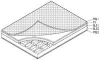
터치 스크린의 터치센서들(TS)은 도 2와 같이 표시패널(DIS)의 상부 편광판(POL1) 상에 적층되거나, 도 3과 같이 상부 편광판(POL1)과 상부 유리기판(GLS1) 사이에 형성될 수 있다.The touch sensors TS of the touch screen are stacked on the upper polarizer POL1 of the display panel DIS as shown in Fig. 2 or formed between the upper polarizer POL1 and the upper glass substrate GLS1 as shown in Fig. 3 .
터치센서들(TS)은 도 4와 같이 표시패널(DIS) 내에 픽셀 어레이와 함께 인셀(In-cell) 타입으로 하부기판에 형성될 수 있다. 도 4와 같이 터치센서들(TS)이 표시패널(DIS)에 내장되는 경우에, Tx 라인들(T1~Tj)에는 픽셀들에 비디오 데이터가 기입될 때(도 8의 WR) 공통전압(Vcom)이 인가되고, 픽셀들에 비디오 데이터가 기입되지 않을 때(도 8의 HB) 터치센서 구동펄스(EXTP)가 인가된다. 따라서, 터치센서들(TS)이 표시패널(DIS)에 내장되는 경우에 Tx 라인들(T1~Tj)에는 공통전압과 터치센서 구동펄스가 스위칭된다.The touch sensors TS may be formed on the lower substrate in an in-cell type together with the pixel array in the display panel DIS as shown in FIG. When the touch sensors TS are embedded in the display panel DIS as shown in FIG. 4, the Tx lines Tl through Tj include a common voltage Vcom ) Is applied, and when the video data is not written to the pixels (HB in Fig. 8), the touch sensor drive pulse EXTP is applied. Accordingly, when the touch sensors TS are embedded in the display panel DIS, the common voltage and the touch sensor drive pulse are switched to the Tx lines T1 to Tj.
도 4와 같이 터치센서들(TS)이 표시패널(DIS) 내에 내장되는 경우에 그 터치센서들(TS)은 픽셀 어레이와 함께 하부 기판 상에 형성될 수 있다. 도 2 내지 도 4에서 "PIX"는 액정셀의 화소전극, "GLS2"는 하부 기판, "POL2"는 하부 편광판을 각각 의미한다.As shown in FIG. 4, when the touch sensors TS are embedded in the display panel DIS, the touch sensors TS may be formed on the lower substrate together with the pixel array. 2 to 4, "PIX" means a pixel electrode of a liquid crystal cell, "GLS2" means a lower substrate, and "POL2" means a lower polarizer.
터치센서들은 정전 용량 방식으로 구현될 수 있다. 이 경우에, 터치 센서들은 게이트라인들(G1~Gn)과 나란한 Tx 라인들(T1~Tj, j는 n 보다 작은 양의 정수), Tx 라인들(T1~Tj)과 교차하고 데이터라인들(D1~Dm)과 나란한 Rx 라인들(R1~Ri, i는 m 보다 작은 양의 정수), 및 Tx 라인들(T1~Tj)과 Rx 라인들(R1~Ri)의 교차부에 형성된 상호 용량(도 6의 MC) 등을 포함한다.The touch sensors can be implemented in a capacitive manner. In this case, the touch sensors cross the Tx lines (T1 to Tj, j is a positive integer smaller than n), the Tx lines (T1 to Tj) and the data lines (T1 to Tj) side by side with the gate lines Formed at the intersection of the Rx lines (R1 to Ri, i is a positive integer smaller than m) and the Tx lines (T1 to Tj) and the Rx lines (R1 to Ri) MC in Fig. 6) and the like.
디스플레이 데이터 구동회로(12)는 다수의 소스 드라이브 IC(Integrated Circuit)을 포함한다. 소스 드라이브 IC들은 시프트 레지스터(Shift register), 래치(Latch), 디지털-아날로그 변환기(Digital to analog converter, DAC), 출력버퍼(output buffer) 등을 포함한다. 소스 드라이브 IC들은 타이밍 콘트롤러(20)으로부터 입력되는 디지털 비디오 데이터(RGB)를 래치한다. 그리고 소스 드라이브 IC들은 디지털 비디오 데이터(RGB)를 아날로그 정극성/부극성 감마보상전압으로 변환하여 아날로그 비디오 데이터전압을 출력한다. 아날로그 비디오 데이터전압은 데이터라인들(D1~Dm)에 공급된다.The display
디스플레이 스캔 구동회로(14)는 하나 이상의 스캔 드라이브 IC를 포함한다. 스캔 드라이브 IC는 레벨시프터(Level shifter), 시프트 레지스터(Shift register) 등을 포함한다. 스캔 드라이브 IC는 동안 타이밍 콘트롤러(20)의 제어 하에 아날로그 비디오 데이터전압에 동기되는 게이트펄스(또는 스캔펄스)를 게이트라인들(G1~Gn)에 순차적으로 공급하여 아날로그 비디오 데이터전압이 기입되는 표시패널(DIS)의 라인을 선택한다. 디스플레이 스캔 구동회로(14)는 게이트 인 패널(Gate in panel, GIP) 공정 기술에 의해 픽셀 어레이와 함께 하부 기판 상에 형성될 수 있다.The display
터치센서 구동회로(18)는 지연된 Tx 타이밍 제어신호(Txcon')에 응답하여 Tx 라인들(T1~Tj)에 터치센서 구동펄스(EXTP)를 순차 출력하여 Tx 라인들(T1~Tj)에 순차적으로 인가하여 터치센서들(TS)을 스캐닝한다. 터치센서 구동펄스(EXTP)는 터치센서 독출회로(16)에 의해 하나의 터치센서 출력신호가 2회 이상 반복 샘플링될 수 있도록 Tx 라인들(T1~Tj) 각각에 2 회 이상 연속 공급된다. 터치센서 구동회로(18)는 디스플레이 스캔 구동회로(14)의 스캔 드라이브 IC와 실질적으로 동일한 회로 구성을 갖는 스캔 드라이브 IC로 구현될 수 있다.The touch
제1 Tx 라인(T1)에 존재하는 터치센서들의 상호 용량(MC)에 충전된 전하들은 제1 Tx 라인(T1)에 공급되는 터치센서 구동펄스(EXTP)에 의해 Rx 라인들(R1~Ri)을 통해 터치센서 독출회로(16)에 입력된다. 제2 Tx 라인(T2)에 존재하는 터치센서들의 상호 용량(MC)에 충전된 전하들은 제2 Tx 라인(T2)에 공급되는 터치센서 구동펄스(EXTP)에 의해 Rx 라인들(R1~Ri)을 통해 터치센서 독출회로(16)에 입력된다. 터치센서 구동회로(18)는 Tx 라인들(T1~Tj) 각각에 2 회 이상 연속으로 터치센서 구동펄스(EXTP)를 공급한다. 예를 들어, 제1 Tx 라인(T1)에 터치센서 구동펄스(EXTP)가 N(여기서, N은 2 이상 20 이하의 양의 정수)회 반복 공급되어 제1 Tx 라인(T1)에 존재하는 터치센서의 출력신호가 터치센서 독출회로(16)에 의해 N회 반복 샘플링된다. 이어서, 제2 Tx 라인(T2)에 터치센서 구동펄스(EXTP)가 N회 반복 공급되어 제2 Tx 라인(T2)에 존재하는 터치센서의 출력신호가 터치센서 독출회로(16)에 의해 N회 반복 샘플링된다. 여기서, N은 터치 스크린의 라인 수와 터치센서 독출회로(16)의 샘플링 동작 특성에 따라 조절될 수 있다.Charges charged in the mutual capacitance MC of the touch sensors existing in the first Tx line T1 are supplied to the Rx lines R1 to Ri by the touch sensor drive pulse EXTP supplied to the first Tx line T1, To the touch sensor readout circuit (16). Charges charged in the mutual capacitance MC of the touch sensors existing in the second Tx line T2 are applied to the Rx lines R1 to Ri by the touch sensor drive pulse EXTP supplied to the second Tx line T2. To the touch sensor readout circuit (16). The touch
터치센서 독출회로(16)는 Rx 타이밍 제어신호(Rxcon)에 응답하여 Rx 라인들(R1~Ri)에 터치 기준전압(Vref)을 공급한다. 터치 기준전압(Vref)은 0V 보다 높고 3V 이하의 직류전압으로 설정될 수 있다. 터치센서 독출회로(16)는 Rx 라인들(R1~Ri)을 통해 입력되는 터치센서들의 아날로그 출력(상호 용량의 전압)의 변화를 샘플링 및 증폭하고, 디지털 터치 데이터로 변환하여 터치 콘트롤러(30)로 전송한다. 터치센서 독출회로(16)는 Rx 라인들(R1~Ri)을 통해 공급되는 전하를 축적하는 적분기의 커패시터를 이용하여 터치센서들의 출력을 샘플링한다. 따라서, 터치센서 독출회로(16)는 적분기의 커패시터에 전하가 충분히 축적되어야만 터치 전후의 변하량을 검출할 수 있다. 이를 위하여, 터치센서 독출회로(16)는 Tx 라인들(T1~Tj)마다 N회 연속적으로 공급되는 터치센서 구동펄스(EXTP)의 폴링에지마다 Rx 라인들(R1~Ri)을 통해 공급되는 터치센서들(TS)의 출력을 샘플링한다.The touch
터치 콘트롤러(30)는 터치센서 독출회로(16)로부터 입력되는 디지털 터치 데이터들을 미리 설정된 터치 인식 알고리즘으로 분석하여 소정의 기준값 이상의 터치 데이터들에 대한 좌표값을 산출한다. 터치 콘트롤러(30)로부터 출력된 터치 위치의 좌표값 데이터는 HID 포맷의 터치 디지털 터치 데이터로서 외부의 호스트 시스템으로 전송된다. 호스트 시스템은 터치 위치의 좌표값과 연계된 응용 프로그램을 실행한다.The
타이밍 콘트롤러(20)는 외부의 호스트 시스템으로부터 입력되는 수직 동기신호(Vsync), 수평 동기신호(Hsync), 데이터 인에이블 신호(Data Enable, DE), 메인 클럭(MCLK) 등의 타이밍신호를 입력받아 디스플레이 데이터 구동회로(12)와 디스플레이 스캔 구동회로(14)의 동작 타이밍을 제어하기 위한 디스플레이 타이밍 제어신호들을 발생한다. 디스플레이 스캔 구동회로(14)의 타이밍 제어신호는 게이트 스타트 펄스(Gate Start Pulse, GSP), 게이트 쉬프트 클럭(Gate Shift Clock, GSC(GCLK)), 게이트 출력 인에이블신호(Gate Output Enable, GOE), 쉬프트 방향 제어신호(DIR) 등을 포함한다. 디스플레이 데이터 구동회로(12)의 타이밍 제어신호는 소스 샘플링 클럭(Source Sampling Clock, SSC), 극성제어신호(Polarity, POL), 및 소스 출력 인에이블신호(Source Output Enable, SOE) 등을 포함한다.The
타이밍 콘트롤러(20)는 터치센서 구동회로(18)의 동작 타이밍을 제어하기 위한 Tx 타이밍 제어신호(Txcon)과, 터치센서 독출회로(16)의 동작 타이밍을 제어하기 위한 Rx 타이밍 제어신호들(Rxcon)을 발생한다. Tx 타이밍 제어신호(Txcon)는 터치센서 구동회로(18) 내에 형성된 시프트 레지스터의 출력을 발생하고 그 출력을 시프트하여 출력하기 위한 스타트 펄스, 시프트 레지스터, 출력 인에이블신호 등을 포함한다. Rx 타이밍 제어신호(Rxcon)는 터치센서 독출회로(16) 내에 형성된 샘플링 스위치의 타이밍 제어신호, ADC(Analog to Digital Convertor) 클럭 등을 포함한다.The
타이밍 콘트롤러(20)는 1 수평기간의 주기를 갖는 타이밍 신호(HDIS)를 동기제어회로에 공급한다. 여기서, 1 수평기간의 주기를 갖는 타이밍 신호(HDIS)는 수평 동기신호(Hsync), 데이터 인에이블 신호(DE), 소스 출력 인에이블신호(SOE), 게이트 시프트 클럭(GSC(GCLK)), 게이트 출력 인에이블 신호 중 어느 하나로 선택될 수 있다. 수평 동기신호(Hsync)는 수평 블랭크기간을 포함하여 1 수평기간의 주기를 가지는 타이밍 신호로서 타이밍 콘트롤러(20)에 입력된다. 데이터 인에이블신호(DE)는 1 수평기간의 주기를 가지며 1 라인의 데이터들과 동기되어 타이밍 콘트롤러(20)에 입력된다. 소스 출력 인에이블신호(SOE)는 1 수평기간의 주기를 가지며 1 수평기간마다 디스플레이 데이터 구동회로(12)로부터 비디오 데이터전압 출력이 발생될 수 있도록 디스플레이 데이터 구동회로(12)의 출력 타이밍을 제어한다. 게이트 시프트 클럭(GSC(GCLK))은 1 수평기간의 주기를 가지며, 디스플레이 게이트 구동회로(14)와 터치센서 구동회로(18) 내에서 1 수평기간 주기로 발생되는 시프트 동작의 타이밍을 제어한다. 게이트 출력 인에이블신호(GOE)는 1 수평기간의 주기를 가지며, 비디오 데이터전압에 동기되어 1 수평기간마다 디스플레이 게이트 구동회로(14)로부터 게이트펄스가 출력될 수 있도록 디스플레이 게이트 구동회로(14)의 출력 타이밍을 제어한다. 선택된 1 수평기간의 주기를 갖는 타이밍 신호(HDIS)는 동기 제어회로의 에지 검출기(22)에 입력된다.The
동기 제어회로는 에지 검출기(22)와 지연기(24)를 포함한다. 동기 제어회로는 타이밍 콘트롤러(20)에 내장될 수 있다.The synchronous control circuit includes an edge detector (22) and a delay (24). The synchronous control circuit may be incorporated in the
에지 검출기(22)는 1 수평기간의 주기를 갖는 타이밍 신호(HDIS)를 입력받아 그 타이밍 신호(HDIS)의 라이징 에지를 검출한다.The
지연기(24)는 에지 검출기(22)로부터 출력되는 에지 검출신호와, 타이밍 콘트롤러(20)로부터 출력되는 Tx 타이밍 제어신호(Txcon)를 입력 받는다. 지연기(24)는 에지 검출기(22)로부터 입력받은 에지 검출신호를 메인클럭(MCLK)으로 계수하고 미리 설정된 계수값만큼 Tx 타이밍 제어신호(Txcon)를 지연시킨다. 그 결과, 터치센서 구동펄스(EXTP)는 지연된 Tx 타이밍 제어신호(Txcon')에 의해 소정 시간만큼 지연되어 그 폴링 에지가 픽셀 구동신호에서 최대 전압이 나타나는 시간을 회피하는 시간에 나타난다. 메인클럭(MCLK)은 타이밍 콘트롤러(20)에 내장된 발진기의 출력 클럭 혹은, 지연기(24) 내에 내장된 발진기의 출력 클럭으로 대신될 수 있다.The
본원 발명자는 터치센서 출력신호에 가장 큰 영향을 주는 픽셀 구동신호 구간(또는 시간)을 실험을 통해 밝혀냈다. 터치센서 출력신호에 가장 큰 영향을 주는 픽셀 구동신호 구간은 픽셀 구동신호에서 게이트펄스와 비디오 데이터전압 등의 최대 전압이 발생되는 시간이다. 실험 결과, 터치센서 출력신호에 가장 큰 영향을 주는 픽셀 구동신호 구간은 게이트펄스가 발생되어 1 수평기간 내에서 픽셀들에 데이터가 충전되는 시간이다. 이하에서, 최대 픽셀 구동신호 구간은 픽셀 어레이의 픽셀들에 데이터가 기입되는 시간으로서 터치센서 출력신호에 가장 큰 영향을 주는 픽셀 구동시간을 의미한다.The inventor of the present invention has experimentally found a pixel drive signal period (or time) that has the greatest effect on the touch sensor output signal. The pixel driving signal period which has the greatest influence on the touch sensor output signal is the time when the maximum voltage such as gate pulse and video data voltage is generated in the pixel driving signal. As a result, the pixel driving signal period which has the greatest influence on the touch sensor output signal is the time when the gate pulse is generated and the data is charged to the pixels within one horizontal period. Hereinafter, the maximum pixel driving signal period refers to the pixel driving time which has the greatest influence on the touch sensor output signal as the time during which data is written to the pixels of the pixel array.
본 발명은 이하의 실시예와 같이, 1 수평기간의 주기를 갖는 타이밍 신호(HDIS)로부터 일정 시간만큼 지연된 시간에 터치센서(TS)의 출력신호를 독출함으로써 최대 픽셀 구동신호 구간을 회피하여 터치센서 출력신호를 읽어낸다. 그리고 본 발명은 터치센서들 각각의 출력을 안정되게 샘플링하기 위하여 터치센서 출력신호 각각을 N회 연속으로 반복 독출한다.The present invention avoids the maximum pixel driving signal period by reading the output signal of the touch sensor TS at a time delayed by a predetermined time from the timing signal HDIS having a period of one horizontal period, Read the output signal. In order to stably sample the output of each of the touch sensors, the present invention sequentially reads each of the touch sensor output signals N times.
도 5는 본 발명의 실시예에 따른 표시장치의 구동 방법을 보여 주는 파형도이다.5 is a waveform diagram showing a driving method of a display device according to an embodiment of the present invention.
도 5를 참조하면, 본 발명의 실시예에 따른 표시장치의 구동 방법은 1 프레임 기간을 디스플레이 기간과 터치센서 구동기간으로 시분할하지 않고 1 프레임 기간 동안 1 라인씩 순차적으로 픽셀들에 비디오 데이터를 기입하되, 최대 픽셀 구동신호 구간들(MAX)을 회피하여 터치센서들 각각의 출력신호를 N회 반복 독출한다.Referring to FIG. 5, a method of driving a display device according to an exemplary embodiment of the present invention includes sequentially writing video data to pixels one line at a time during one frame period, without time-dividing one frame period into a display period and a touch sensor driving period The maximum pixel driving signal intervals MAX are avoided and the output signals of the touch sensors are repeatedly read out N times.
최대 픽셀 구동 신호 구간들(MAX)은 게이트펄스에 의해 화소전극에 접속된 TFT가 턴-온되어 비디오 데이터전압이 화소전극에 충전되는 시간이다. 최대 픽셀 구동신호 구간들(MAX) 사이에는 수평 블랭크 시간(Horizontal blank time)을 포함한 최대 픽셀 구동 신호 구간의 회피 시간이 존재한다. 터치센서 구동펄스(EXTP)의 폴링 에지는 1 수평기간의 타이밍 신호 지연으로 인하여 수평 블랭크 시간 내에 나타난다. 터치센서 독출회로(16)는 터치센서 구동펄스(EXTP)의 폴링 에지마다 Rx 라인들(R1~Rx)을 통해 터치센서의 출력신호를 샘플링한다. 따라서, 터치센서 각각의 출력은 연속되는 N 개의 수평 블랭크 시간마다 N회 반복 샘플링된다.The maximum pixel drive signal intervals MAX are the time when the TFT connected to the pixel electrode by the gate pulse is turned on and the video data voltage is charged to the pixel electrode. There is a avoiding time of the maximum pixel driving signal interval including the horizontal blank time between the maximum pixel driving signal intervals MAX. The falling edge of the touch sensor drive pulse EXTP appears within the horizontal blank time due to the timing signal delay in one horizontal period. The touch
도 5에서 "1TStime"은 하나의 터치센서 출력신호를 안정적으로 샘플링하는데 필요한 시간이고, 이 시간(1TStime)은 N 개의 터치 스캐닝기간(Tscan1~TscanN)으로 나뉘어진다.In Fig. 5, "1TStime" is a time required to stably sample one touch sensor output signal, and this time (1TStime) is divided into N touch scanning periods (Tscan1 to TscanN).
터치 스캐닝기간(Tscan1~TscanN) 각각은 수평 블랭크 시간을 포함한다. 하나의 터치센서의 출력신호는 N회(Tscan1~TscanN) 반복 연속으로 독출된다. 예를 들어, 터치 스크린의 제1 라인에 존재하는 제1 터치센서의 출력은 터치 스캐닝기간(Tscan1~TscanN) 마다 연속으로 Rx 라인들(R1~Ri)을 통해 터치센서 독출회로(16)에 입력되어 그 터치센서 독출회로(16)의 적분기에 의해 샘플링된다. 이어서, 터치 스크린의 제2 라인에 존재하는 제2 터치센서의 출력은 터치 스캐닝기간(도시하지 않은 TscanN+1~Tscan2N) 마다 연속으로 Rx 라인들(R1~Ri)을 통해 터치센서 독출회로(16)에 입력되어 그 터치센서 독출회로(16)의 적분기에 의해 샘플링된다.Each of the touch scanning periods Tscan1 to TscanN includes a horizontal blank time. The output signal of one touch sensor is read out repeatedly N times (Tscan1 to TscanN). For example, the output of the first touch sensor existing in the first line of the touch screen is continuously supplied to the touch
도 6은 터치센서들(TS)과 터치센서 구동펄스(EXTP)를 보여 주는 등가 회로도이다.6 is an equivalent circuit diagram showing the touch sensors TS and the touch sensor driving pulse EXTP.
도 6을 참조하면, 터치센서들(TS)은 Tx 라인들(T1~T4), Tx 라인들(T1~T4)과 교차되는 Rx 라인들(R1~R5), 및 Tx 라인들(T1~T4)과 Rx 라인들(R1~R5)의 교차부에 형성된 상호 용량들(MC)을 포함한다.6, the touch sensors TS include Tx lines T1 to T4, Rx lines R1 to R5 that cross Tx lines T1 to T4, and Tx lines T1 to T4 And mutual capacitances MC formed at the intersections of the Rx lines R1 to R5.
Tx 라인들(T1~T4)에는 터치센서 구동회로(18)에 의해 터치센서 구동펄스(EXTP)가 순차적으로 공급된다. 여기서, Tx 라인들(T1~T4) 각각에 공급되는 터치센서 구동펄스(EXTP)는 N회 연속으로 공급된다. 터치센서 독출회로(16)는 Rx 라인들(R1~R5)를 통해 입력 받은 상호 용량들(MC)의 출력을 터치센서 구동펄스(EXTP)의 폴링 에지마다 샘플링한다.A touch sensor drive pulse (EXTP) is sequentially supplied to the Tx lines (T1 to T4) by the touch sensor drive circuit (18). Here, the touch sensor drive pulse EXTP supplied to each of the Tx lines T1 to T4 is supplied N times in succession. The touch
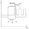
도 7은 터치센서 구동펄스(EXTP)와 1 수평기간의 주기를 갖는 타이밍 신호(HDIS)를 보여 주는 파형도이다.7 is a waveform diagram showing a timing signal HDIS having a period of one horizontal period and a touch sensor drive pulse EXTP.
도 7을 참조하면, 동기 제어회로는 1 수평기간의 주기를 갖는 타이밍 신호(HDIS)를 기준으로 소정 시간(D)만큼 Tx 타이밍 제어신호(Txcon)를 지연시킨다. 여기서, 소정 시간(D)은 1 수평기간의 주기를 갖는 타이밍 신호(HDIS)의 라이징 에지로부터 클럭신호를 계수하여 판단될 수 있다. 소정 시간(D)은 터치센서 구동펄스(EXTP)의 폴링 에지가 최대 픽셀 구동신호 구간을 회피하는 시간에 발생되도록 미리 설정된다.Referring to FIG. 7, the synchronization control circuit delays the Tx timing control signal Txcon by a predetermined time D based on the timing signal HDIS having a period of one horizontal period. Here, the predetermined time D may be determined by counting the clock signal from the rising edge of the timing signal HDIS having a period of one horizontal period. The predetermined time D is preset so that the falling edge of the touch sensor drive pulse EXTP is generated at the time of avoiding the maximum pixel drive signal period.
도 8은 도 1에 도시된 표시장치의 픽셀들에 공급되는 픽셀 구동신호들과, 터치 스크린의 터치센서들에 공급되는 터치센서 구동펄스를 보여 주는 파형도이다.FIG. 8 is a waveform diagram showing pixel driving signals supplied to the pixels of the display device shown in FIG. 1 and a touch sensor driving pulse supplied to the touch sensors of the touch screen.
도 8을 참조하면, 1 수평기간(1H)은 표시패널(DIS)의 1 수평라인을 스캐닝하는 시간이다. 1 수평기간은 데이터 기입기간(WR)과 수평 블랭크기간(HB)을 포함한다. 수평 블랭크기간(HB)은 1 수평기간(1H)에서 데이터 기입기간을 뺀 시간이다.Referring to FIG. 8, one horizontal period (1H) is a time for scanning one horizontal line of the display panel DIS. One horizontal period includes a data writing period WR and a horizontal blanking period HB. The horizontal blank period HB is a time obtained by subtracting the data writing period from one horizontal period (1H).
최대 픽셀 구동신호 구간은 데이터 기입기간(WR)을 포함한다. 데이터 기입기간(WR)에는 게이트펄스가 발생되고 그 게이트펄스에 응답하여 픽셀들의 화소전극에 비디오 데이터전압이 공급된다.The maximum pixel driving signal period includes a data writing period WR. In the data writing period WR, a gate pulse is generated and the video data voltage is supplied to the pixel electrode of the pixels in response to the gate pulse.
최대 픽셀 구동신호 구간을 회피하는 시간은 수평 블랭크기간(HB)을 포함한다. 수평 블랭크기간(HB)은 앞선 게이트펄스의 폴링에지와 그 다음 게이트펄스의 라이징 에지 사이의 기간이다. 수평 블랭크기간(HB)에는 픽셀들에 데이터전압이 기입되지 않는다.The time for avoiding the maximum pixel drive signal period includes the horizontal blank period HB. The horizontal blanking period HB is the period between the falling edge of the preceding gate pulse and the rising edge of the next gate pulse. In the horizontal blank period HB, no data voltage is written to the pixels.
Tx 라인들(T1~T3)에는 터치센서 구동펄스(EXTP)가 순차적으로 공급된다. 여기서, Tx 라인들(T1~T3) 각각에는 터치센서 구동펄스(EXTP)가 N 회 연속으로 공급되고, 그 터치센서 구동펄스(EXTP)의 폴링 에지가 수평 블랭크기간(HB) 내에 존재한다. 도 8은 Tx 라인들(T1~T3) 각각에는 터치센서 구동펄스(EXTP)가 3 회 연속으로 공급되는 예를 보여 준다. Tx 라인들(T1~T3) 각각에 연속으로 공급되는 터치센서 구동펄스(EXTP)의 횟수는 3회로로 한정되지 않는다.A touch sensor drive pulse EXTP is sequentially supplied to the Tx lines T1 to T3. Here, the touch sensor drive pulse EXTP is supplied to the Tx lines T1 to T3 successively N times, and the falling edge of the touch sensor drive pulse EXTP is present in the horizontal blank period HB. 8 shows an example in which the touch sensor drive pulse EXTP is supplied three times in succession to each of the Tx lines T1 to T3. The number of times of the touch sensor drive pulse EXTP supplied continuously to each of the Tx lines T1 to T3 is not limited to three.
제1 Tx 라인(T1)에는 제1 내지 제3 터치센서 구동펄스(EXTP)가 연속으로 공급되고, 제1 내지 제3 터치센서 구동펄스(EXTP)의 폴링 에지가 수평 블랭크기간(HB)에 존재한다. 이어서, 제2 Tx 라인(T2)에는 제4 내지 제6 터치센서 구동펄스(EXTP)가 연속으로 공급되고, 제4 내지 제6 터치센서 구동펄스(EXTP)의 폴링 에지가 수평 블랭크기간(HB)에 존재한다. 이어서, 제3 Tx 라인(T3)에는 제7 내지 제9 터치센서 구동펄스(EXTP)가 연속으로 공급되고, 제7 내지 제9 터치센서 구동펄스(EXTP)의 폴링 에지가 수평 블랭크기간(HB)에 존재한다. 터치센서 독출회로(16)는 터치센서 구동펄스(EXTP)의 폴링 에지마다 Rx 라인들(R1~Ri)을 통해 터치센서들(TS)의 출력을 샘플링한다.The first to third touch sensor drive pulses EXTP are continuously supplied to the first Tx line T1 and the falling edge of the first to third touch sensor drive pulses EXTP is present in the horizontal blank period HB do. The fourth to sixth touch sensor drive pulses EXTP are continuously supplied to the second Tx line T2 and the falling edge of the fourth to sixth touch sensor drive pulses EXTP is supplied to the horizontal blank period HB. Lt; / RTI > The seventh to ninth touch sensor drive pulses EXTP are supplied to the third Tx line T3 continuously and the falling edge of the seventh to ninth touch sensor drive pulses EXTP is supplied to the horizontal blank period HB. Lt; / RTI > The touch
본원 발명자는 본 발명의 효과를 비교 평가하기 위하여 도 1과 같은 표시장치를 도 5 내지 도 8과 같은 방법으로 구동하여 터치센서 구동펄스(EXTP)의 지연 유무에 따라 비교 평가 실험을 실시하였다.In order to comparatively evaluate the effects of the present invention, the present inventor conducted a comparative evaluation test according to the presence or absence of a delay of the touch sensor driving pulse EXTP by driving the display device as shown in FIG.
도 9는 터치센서 구동펄스(EXTP)가 지연되지 않은 실험 조건 파형을 보여 주는 파형도이고, 도 10은 도 9와 같은 터치센서 구동펄스(EXTP)를 Tx 라인들에 공급한 실험에서 측정된 터치센서들의 출력을 보여 주는 실험 결과 도면이다. 도 11은 터치센서 구동펄스(EXTP)의 폴링 에지가 최대 픽셀 구동신호 구간을 회피하도록 터치센서 구동펄스(EXTP)를 소정 시간만큼 지연한 실험 조건 파형을 보여 주는 파형도이다. 도 12는 도 11과 같은 터치센서 구동펄스(EXTP)를 Tx 라인들에 공급한 실험에서 측정된 터치센서들의 출력을 보여 주는 실험 결과 도면이다. 도 9 및 도 11에서, x축은 시간이고 y축은 전압이다. 도 10 및 도 12에서 x축은 터치 스크린의 x축을 따라 일렬로 배열된 터치센서들의 번호이고, y축은 터치센서 독출회로(16)에 의해 디지털 터치 데이터로 변환된 터치센서 출력 값들이다.9 is a waveform chart showing an experiment condition waveform in which the touch sensor drive pulse EXTP is not delayed, and FIG. 10 is a waveform diagram showing a touch test pulse in the experiment in which the touch sensor drive pulse EXTP shown in FIG. 9 is supplied to the Tx lines. The experimental results show the output of the sensors. 11 is a waveform diagram showing an experiment condition waveform in which the touch sensor drive pulse EXTP is delayed by a predetermined time so that the falling edge of the touch sensor drive pulse EXTP avoids the maximum pixel drive signal interval. 12 is an experimental result showing the output of the touch sensors measured in the experiment in which the touch sensor drive pulse EXTP shown in FIG. 11 is supplied to the Tx lines. 9 and 11, the x-axis is time and the y-axis is voltage. 10 and 12, the x-axis is the number of touch sensors arranged in a row along the x-axis of the touch screen, and the y-axis is the touch sensor output values converted into digital touch data by the touch
실험에서 사용된 표시장치는 도 1과 같은 회로 구성을 포함하고 디스플레이 스캔 구동회로(14)가 게이트 인 패널(GIP) 형태로 픽셀 어레이에 함께 하부 기판에 형성되었다. 도 9 내지 도 12의 실험에서, 터치센서 구동펄스(EXTP)의 타이밍 기준으로 적용된 1 수평기간의 주기를 갖는 타이밍 신호(HDIS)는 디스플레이 스캔 구동회로(14)와 터치센서 구동회로(18)의 게이트 쉬프트 클럭(GCLK)으로 선택되었다. 실험에서 적용된 터치센서 구동펄스(EXTP)의 1 주기는 16μsec이고, 게이트 쉬프트 클럭(GCLK)의 1 주기는 10μsec이다.The display device used in the experiment includes the circuit configuration as shown in Fig. 1, and the display
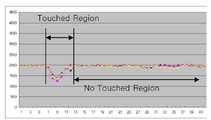
도 9와 같이, 터치센서 구동펄스(EXTP)가 지연되지 않으면 그 터치센서 구동펄스(EXTP)의 폴링 에지가 최대 픽셀 구동신호 구간 내에 발생된다. 이 경우에, 터치센서 구동펄스(EXTP)의 폴링 에지에서 터치센서들의 출력을 측정하면 도 10과 같이 최대 픽셀 구동신호 구간에서 발생되는 게이트펄스 전압과 비디오 데이터전압의 영향으로 인하여, 터치영역(Touched Region)과 비 터치영역에서 독출된 터치센서들의 전압이 매 측정마다 다르게 측정되었다. 도 10의 실험 결과와 같이, 매 측정마다 측정치가 다르게 되면, 터치 전후를 판단하기가 어렵기 때문에 터치센서의 출력신호 신뢰성이 낮아지고 터치 감도가 낮아진다.As shown in FIG. 9, if the touch sensor driving pulse EXTP is not delayed, a falling edge of the touch sensor driving pulse EXTP is generated within the maximum pixel driving signal interval. In this case, when the output of the touch sensors is measured at the polling edge of the touch sensor driving pulse EXTP, due to the influence of the gate pulse voltage and the video data voltage generated in the maximum pixel driving signal interval as shown in FIG. 10, The voltage of the touch sensor read out from the region and the non-touch region was measured differently for each measurement. As shown in the experimental result of FIG. 10, if the measurement value is different for each measurement, it is difficult to determine before and after the touch, so that the reliability of the output signal of the touch sensor is lowered and the touch sensitivity is lowered.
도 11과 같이 터치센서 구동펄스(EXTP)를 소정시간(실험에서 대략 12μsec) 만큼 지연하여 그 터치센서 구동펄스(EXTP)의 폴링 에지가 최대 픽셀 구동신호 구간을 회피하면, 도 12와 같이 터치센서들의 출력이 터치영역과 비터치영역에서 큰 차이를 보이고 매 측정치가 비슷한 결과로 측정되었다. 따라서, 터치센서 구동펄스(EXTP)를 지연시킴으로써 최대 픽셀 구동신호 구간을 회피하여 터치센서들을 샘플링하여 터치센서들의 출력신호 신뢰성을 높이고 터치 감도를 높일 수 있다는 것이 확인되었다.
When the touch sensor driving pulse EXTP is delayed by a predetermined time (about 12 microseconds in the experiment) and the falling edge of the touch sensor driving pulse EXTP avoids the maximum pixel driving signal interval, as shown in FIG. 12, The results show that there is a large difference between the touch and non - touch areas and each measurement is measured with similar results. Accordingly, it has been confirmed that by delaying the touch sensor driving pulse EXTP, the maximum pixel driving signal interval is avoided and the touch sensors are sampled to increase the output signal reliability of the touch sensors and to increase the touch sensitivity.
DIS : 표시패널TS : 터치센서
12 : 디스플레이 데이터 구동회로14 : 디스플레이 스캔 구동회로
16 : 터치센서 독출회로18 : 터치센서 구동회로
20 : 타이밍 콘트롤러22 : 에지 검출기
24 : 지연기30 : 터치 콘트롤러DIS: Display panel TS: Touch sensor
12: display data driving circuit 14: display scan driving circuit
16: touch sensor dock circuit 18: touch sensor driving circuit
20: timing controller 22: edge detector
24: Delay device 30: Touch controller
Claims (9)
Translated fromKoreanTx 라인들과 Rx 라인들이 교차되고 상기 Tx 라인들과 상기 Rx 라인들의 교차부에 터치센서들이 형성된 터치 스크린;
1 프레임기간 동안 1 수평기간 내의 데이터 기입기간마다 상기 픽셀들에 데이터전압을 기입하는 디스플레이 구동회로;
상기 Tx 라인들에 소정 시간만큼 지연된 터치센서 구동펄스를 순차적으로 공급하되, 상기 Tx 라인들 각각에 상기 터치센서 구동펄스를 2회 이상 연속으로 공급하는 터치 스크린 구동회로;
상기 디스플레이 구동회로와 상기 터치 스크린 구동회로의 동작 타이밍을 제어하고 상기 디스플레이 구동회로에 디지털 비디오 데이터를 공급하는 타이밍 콘트롤러; 및
상기 1 수평기간의 주기를 갖는 타이밍 신호를 클럭신호로 계수하여 상기 소정 시간 만큼 상기 타이밍 콘트롤러로부터 출력된 Tx 타이밍 제어신호를 지연하는 동기 제어회로를 포함하고,
상기 터치센서 구동펄스들 각각의 폴링 에지는 상기 1 수평기간에서 상기 데이터 기입기간을 뺀 수평 블랭크 기간 내에 존재하고,
상기 터치 스크린 구동회로는 상기 Rx 라인들을 통해 수신되는 터치센서 출력신호를 상기 터치센서 구동펄스의 폴링 에지에 동기하여 샘플링하며,
상기 터치 스크린 구동회로는 상기 지연된 Tx 타이밍 제어신호에 응답하여 상기 터치센서 구동펄스를 발생하는 것을 특징으로 하는 터치센서를 가지는 표시장치.
A pixel array in which data lines and gate lines are crossed and pixels are arranged in a matrix form;
A touch screen in which Tx lines and Rx lines intersect and touch sensors are formed at intersections of the Tx lines and the Rx lines;
A display driving circuit for writing a data voltage to the pixels in each data writing period in one horizontal period during one frame period;
A touch screen driving circuit for sequentially supplying a touch sensor driving pulse delayed by a predetermined time to the Tx lines and continuously supplying the touch sensor driving pulse to each of the Tx lines two or more times;
A timing controller for controlling operation timings of the display driving circuit and the touch screen driving circuit and supplying digital video data to the display driving circuit; And
And a synchronization control circuit which counts a timing signal having a period of one horizontal period as a clock signal and delays the Tx timing control signal output from the timing controller by the predetermined time,
Wherein the falling edge of each of the touch sensor driving pulses is within a horizontal blank period obtained by subtracting the data writing period from the one horizontal period,
Wherein the touch screen driving circuit samples the touch sensor output signal received through the Rx lines in synchronization with a polling edge of the touch sensor driving pulse,
Wherein the touch screen driving circuit generates the touch sensor driving pulse in response to the delayed Tx timing control signal.
상기 터치 스크린은 상기 픽셀 어레이와 함께 표시패널 내에 배치되는 것을 특징으로 하는 터치센서를 가지는 표시장치.
The method according to claim 1,
Wherein the touch screen is disposed within the display panel together with the pixel array.
상기 1 수평기간의 주기를 갖는 타이밍 신호는, 수평 동기신호, 데이터 인에이블 신호, 소스 출력 인에이블신호, 게이트 시프트 클럭, 게이트 출력 인에이블 신호 중 어느 하나를 포함하는 것을 특징으로 하는 터치센서를 가지는 표시장치.
The method according to claim 1,
Wherein the timing signal having the period of one horizontal period includes any one of a horizontal synchronizing signal, a data enable signal, a source output enable signal, a gate shift clock, and a gate output enable signal. Display device.
상기 터치 스크린 구동회로는,
제1 Tx 라인에 상기 터치센서 구동펄스를 2회 이상 연속으로 공급한 후에,
제2 Tx 라인에 상기 터치센서 구동펄스를 2회 이상 연속으로 공급한 다음,
제3 Tx 라인에 상기 터치센서 구동펄스를 2회 이상 연속으로 공급하고,
상기 터치센서 구동펄스 각각의 폴링 에지마다 상기 Rx 라인들을 통해 터치센서들의 출력을 샘플링하는 것을 특징으로 하는 터치센서를 가지는 표시장치.
The method according to claim 1,
The touch screen driving circuit includes:
After the touch sensor drive pulse is continuously supplied to the first Tx line two or more times,
The touch sensor driving pulse is continuously supplied to the second Tx line two or more times,
The touch sensor driving pulse is continuously supplied to the third Tx line two or more times,
And sampling the outputs of the touch sensors through the Rx lines for each of the falling edges of the touch sensor drive pulses.
1 프레임기간 동안 1 수평기간 내의 데이터 기입기간마다 상기 픽셀들에 데이터전압을 기입하는 단계;
상기 Tx 라인들에 소정 시간만큼 지연된 터치센서 구동펄스를 순차적으로 공급하되, 상기 Tx 라인들 각각에 상기 터치센서 구동펄스를 2회 이상 연속으로 공급하는 단계;
상기 1 수평기간의 주기를 갖는 타이밍 신호를 발생하는 단계; 및
상기 1 수평기간의 주기를 갖는 타이밍 신호를 클럭신호로 계수하여 상기 소정 시간 만큼 Tx 타이밍 제어신호를 지연하는 단계를 포함하고,
상기 터치센서 구동펄스들 각각의 폴링 에지는 상기 1 수평기간에서 상기 데이터 기입기간을 뺀 수평 블랭크 기간 내에 존재하고,
상기 Rx 라인들을 통해 수신되는 터치센서 출력신호는 상기 터치센서 구동펄스의 폴링 에지에 동기되어 샘플링되며,
상기 터치센서 구동펄스가 상기 지연된 Tx 타이밍 제어신호에 기초하여 발생되는 것을 특징으로 하는 터치센서를 가지는 표시장치의 구동방법.
A pixel array in which data lines and gate lines are crossed and pixels are arranged in a matrix form, and a touch including a touch screen in which Tx lines and Rx lines are crossed and touch sensors are formed at intersections of the Tx lines and the Rx lines A method of driving a display device having a sensor,
Writing a data voltage to the pixels in each data writing period in one horizontal period during one frame period;
Sequentially supplying a touch sensor driving pulse delayed by a predetermined time to the Tx lines, and continuously supplying the touch sensor driving pulse to each of the Tx lines at least two times;
Generating a timing signal having a period of one horizontal period; And
And delaying the Tx timing control signal by the predetermined time by counting a timing signal having a period of one horizontal period as a clock signal,
Wherein the falling edge of each of the touch sensor driving pulses is within a horizontal blank period obtained by subtracting the data writing period from the one horizontal period,
The touch sensor output signal received through the Rx lines is sampled in synchronization with the falling edge of the touch sensor driving pulse,
And the touch sensor drive pulse is generated based on the delayed Tx timing control signal.
상기 1 수평기간의 주기를 갖는 타이밍 신호는, 수평 동기신호, 데이터 인에이블 신호, 소스 출력 인에이블신호, 게이트 시프트 클럭, 게이트 출력 인에이블 신호 중 어느 하나를 포함하는 것을 특징으로 하는 터치센서를 가지는 표시장치의 구동방법.
The method according to claim 6,
Wherein the timing signal having the period of one horizontal period includes any one of a horizontal synchronizing signal, a data enable signal, a source output enable signal, a gate shift clock, and a gate output enable signal. A method of driving a display device.
상기 Tx 라인들에 소정 시간만큼 지연된 터치센서 구동펄스를 순차적으로 공급하되, 상기 Tx 라인들 각각에 상기 터치센서 구동펄스를 2회 이상 연속으로 공급하는 단계는,
제1 Tx 라인에 상기 터치센서 구동펄스를 2회 이상 연속으로 공급하는 단계;
제2 Tx 라인에 상기 터치센서 구동펄스를 2회 이상 연속으로 공급한 단계;
제3 Tx 라인에 상기 터치센서 구동펄스를 2회 이상 연속으로 공급하는 단계; 및
상기 터치센서 구동펄스 각각의 폴링 에지마다 상기 Rx 라인들을 통해 터치센서들의 출력을 샘플링하는 단계를 포함하는 것을 특징으로 하는 터치센서를 가지는 표시장치의 구동방법.The method according to claim 6,
Sequentially supplying a touch sensor driving pulse delayed by a predetermined time to the Tx lines, and continuously supplying the touch sensor driving pulse to each of the Tx lines two or more times,
Continuously supplying the touch sensor driving pulse to the first Tx line twice or more times;
Continuously supplying the touch sensor driving pulse to the second Tx line twice or more times;
Continuously supplying the touch sensor driving pulse to the third Tx line twice or more times; And
And sampling the output of the touch sensors through the Rx lines for each of the falling edges of the touch sensor drive pulses.
Priority Applications (4)
| Application Number | Priority Date | Filing Date | Title |
|---|---|---|---|
| KR1020110032100AKR101819678B1 (en) | 2011-04-07 | 2011-04-07 | Display having touch sensor and driving method thereof |
| CN201210099917.2ACN102736811B (en) | 2011-04-07 | 2012-04-06 | Display device having touch sensor and method for driving the same |
| TW101112327ATWI467434B (en) | 2011-04-07 | 2012-04-06 | Display device having touch sensor and method for driving the same |
| US13/442,548US9310942B2 (en) | 2011-04-07 | 2012-04-09 | Display device having touch sensor reducing limit in driving time of pixel array and driving time of touch sensor and method for driving the same |
Applications Claiming Priority (1)
| Application Number | Priority Date | Filing Date | Title |
|---|---|---|---|
| KR1020110032100AKR101819678B1 (en) | 2011-04-07 | 2011-04-07 | Display having touch sensor and driving method thereof |
Publications (2)
| Publication Number | Publication Date |
|---|---|
| KR20120114534A KR20120114534A (en) | 2012-10-17 |
| KR101819678B1true KR101819678B1 (en) | 2018-01-17 |
Family
ID=46965707
Family Applications (1)
| Application Number | Title | Priority Date | Filing Date |
|---|---|---|---|
| KR1020110032100AActiveKR101819678B1 (en) | 2011-04-07 | 2011-04-07 | Display having touch sensor and driving method thereof |
Country Status (4)
| Country | Link |
|---|---|
| US (1) | US9310942B2 (en) |
| KR (1) | KR101819678B1 (en) |
| CN (1) | CN102736811B (en) |
| TW (1) | TWI467434B (en) |
Families Citing this family (37)
| Publication number | Priority date | Publication date | Assignee | Title |
|---|---|---|---|---|
| JP5734805B2 (en)* | 2011-10-12 | 2015-06-17 | 株式会社ジャパンディスプレイ | Display device, driving circuit, driving method, and electronic apparatus |
| KR101908501B1 (en)* | 2011-12-07 | 2018-10-17 | 엘지디스플레이 주식회사 | Integrated Touch Screen With Organic Emitting Display Device and Method for Manufacturing the Same |
| JP2015148830A (en)* | 2012-05-28 | 2015-08-20 | シャープ株式会社 | Coordinate output device, display device, coordinate output method, and program |
| US9158405B2 (en)* | 2012-06-15 | 2015-10-13 | Blackberry Limited | Electronic device including touch-sensitive display and method of controlling same |
| JP6050728B2 (en) | 2012-07-24 | 2016-12-21 | 株式会社ジャパンディスプレイ | Liquid crystal display device with touch sensor and electronic device |
| TWI475441B (en)* | 2012-10-19 | 2015-03-01 | Au Optronics Corp | In-cell touch display panel and driving method thereof |
| KR101305924B1 (en)* | 2012-10-23 | 2013-09-09 | 엘지디스플레이 주식회사 | Display device and driving method thereof |
| KR101993220B1 (en) | 2012-10-29 | 2019-06-26 | 엘지디스플레이 주식회사 | Display device with integrated touch screen |
| KR101667078B1 (en)* | 2012-10-30 | 2016-10-18 | 엘지디스플레이 주식회사 | Touch sensing device, system and enhancement method of touch report rate thereof |
| TWI489175B (en)* | 2012-11-30 | 2015-06-21 | Au Optronics Corp | Array substrate of a display panel and the driving method thereof |
| KR102009886B1 (en)* | 2012-12-04 | 2019-08-12 | 엘지디스플레이 주식회사 | Touch sensing display divice |
| KR101682964B1 (en)* | 2012-12-09 | 2016-12-06 | 엘지디스플레이 주식회사 | Display Device and Method for touch sensing of the same |
| KR101447542B1 (en)* | 2013-01-11 | 2014-10-08 | 주식회사 하이딥 | Touch panel input apparatus and dirving method for the same |
| TWI488083B (en)* | 2013-01-11 | 2015-06-11 | Au Optronics Corp | Method using touch sensing ic to control display driving ic and system using the same |
| KR102057660B1 (en) | 2013-03-07 | 2019-12-23 | 삼성디스플레이 주식회사 | Display Device Integrated Touch Screen Panel and Driving Method Thereof |
| KR102011435B1 (en)* | 2013-03-07 | 2019-08-19 | 삼성디스플레이 주식회사 | Display Device Integrated Touch Screen Panel and Driving Method Thereof |
| KR102193997B1 (en)* | 2013-04-17 | 2020-12-22 | 삼성전자주식회사 | Coordinate measuring apparaturs which measures input position of coordinate indicating apparatus |
| CN103680410B (en)* | 2013-12-23 | 2016-01-06 | 京东方科技集团股份有限公司 | Based on the touch-control display drive method of AMOLED |
| KR102081132B1 (en)* | 2013-12-30 | 2020-02-25 | 엘지디스플레이 주식회사 | Organic Light Emitting Display |
| US9880649B2 (en) | 2014-09-29 | 2018-01-30 | Apple Inc. | Touch, pen and force sensor operation with variable refresh displays |
| CN104461138B (en)* | 2014-12-05 | 2017-07-04 | 京东方科技集团股份有限公司 | The driving method of touch-control display panel, device and touch-control display panel |
| CN104432543B (en)* | 2014-12-12 | 2018-02-13 | 卓尔悦欧洲控股有限公司 | Electronic cigarette battery device and its electronic cigarette |
| US9910533B2 (en) | 2015-06-19 | 2018-03-06 | Apple Inc. | Timing scheme for touch screen supporting variable refresh rate |
| CN104978068B (en)* | 2015-07-17 | 2019-03-01 | 京东方科技集团股份有限公司 | Touch display driving method, system, display device and application processor |
| KR102340937B1 (en)* | 2015-07-31 | 2021-12-20 | 엘지디스플레이 주식회사 | Stylus pen and touch sensing system and driving method of the same |
| TWI576738B (en)* | 2015-11-04 | 2017-04-01 | 友達光電股份有限公司 | Shift register |
| TWI588810B (en)* | 2015-11-27 | 2017-06-21 | 友達光電股份有限公司 | Display driving method and mobile apparatus thereof |
| CN106061072A (en)* | 2016-07-22 | 2016-10-26 | 肇庆市小凡人科技有限公司 | Intelligent control system of lighting device |
| KR102612735B1 (en)* | 2016-09-30 | 2023-12-13 | 엘지디스플레이 주식회사 | Display Device Having Touch Sensor |
| KR102314497B1 (en)* | 2016-10-25 | 2021-10-20 | 엘지디스플레이 주식회사 | Touch display device, active pen, touch system, touch circuit, and pen recognition method |
| US10474286B2 (en)* | 2016-10-25 | 2019-11-12 | Lg Display Co., Ltd. | Touch display device, active pen, touch system, touch circuit, and pen recognition method |
| US10088965B2 (en)* | 2016-12-16 | 2018-10-02 | Stmicroelectronics Asia Pacific Pte Ltd | Reduction of noise in touch data samples via sampling during porch time of Vsync and Hsync signals |
| TWI637371B (en)* | 2017-12-28 | 2018-10-01 | 友達光電股份有限公司 | Shift register circuit |
| TWI662455B (en)* | 2018-05-31 | 2019-06-11 | 友達光電股份有限公司 | Touch display device and control method thereof |
| JP7041035B2 (en)* | 2018-09-27 | 2022-03-23 | シャープ株式会社 | Touch panel control device, touch panel control method, and input display device |
| CN109669583B (en)* | 2019-01-04 | 2021-09-10 | 京东方科技集团股份有限公司 | Touch display device and driving method of touch display panel |
| JP7301635B2 (en)* | 2019-07-02 | 2023-07-03 | シャープ株式会社 | Touch panel control device, touch panel control method, and input display device |
Citations (2)
| Publication number | Priority date | Publication date | Assignee | Title |
|---|---|---|---|---|
| US20050162448A1 (en) | 2004-01-28 | 2005-07-28 | Seiko Epson Corporation | Electro-optical device, driving circuit of electro-optical device, driving method of electro-optical device, and electronic apparatus |
| US20110310054A1 (en) | 2010-06-21 | 2011-12-22 | Avago Technologies Ecbu Ip (Singapore) Pte. Ltd. | Capacitive Touchscreen Signal Acquisition without Panel Reset |
Family Cites Families (13)
| Publication number | Priority date | Publication date | Assignee | Title |
|---|---|---|---|---|
| JP2007163877A (en)* | 2005-12-14 | 2007-06-28 | Toshiba Matsushita Display Technology Co Ltd | Array substrate and display apparatus |
| US8040326B2 (en) | 2007-06-13 | 2011-10-18 | Apple Inc. | Integrated in-plane switching display and touch sensor |
| US8941394B2 (en)* | 2008-06-25 | 2015-01-27 | Silicon Laboratories Inc. | Capacitive sensor system with noise reduction |
| RU2451983C1 (en)* | 2008-09-02 | 2012-05-27 | Шарп Кабусики Кайся | Display device |
| KR101322957B1 (en)* | 2008-10-10 | 2013-10-29 | 엘지디스플레이 주식회사 | Touch sensor and driving method thereof |
| JP2010108501A (en)* | 2008-10-30 | 2010-05-13 | Samsung Electronics Co Ltd | Touch screen controller having increased sensing sensitivity, and display driving circuit and display device and system having the touch screen controller |
| CN102460357B (en)* | 2009-05-29 | 2016-04-27 | 3M创新有限公司 | High-speed multi-touch touch device and its controller |
| JP5513933B2 (en)* | 2009-06-30 | 2014-06-04 | 株式会社ジャパンディスプレイ | Touch sensor and display device |
| KR101552988B1 (en)* | 2009-07-10 | 2015-09-14 | 엘지디스플레이 주식회사 | Driving circuit for liquid crystal display device and method for driving the same |
| TWI395126B (en)* | 2009-07-20 | 2013-05-01 | Mstar Semiconductor Inc | Sensing apparatus and method applied to touch screen |
| TWI421820B (en)* | 2009-10-16 | 2014-01-01 | Ind Tech Res Inst | Display device, control method, and electronic system utilizing the same |
| EP2491478A4 (en)* | 2009-10-20 | 2014-07-23 | Cypress Semiconductor Corp | Method and apparatus for reducing coupled noise influence in touch screen controllers. |
| JP5382658B2 (en) | 2010-02-26 | 2014-01-08 | 株式会社ジャパンディスプレイ | Display device with touch sensor, touch panel, touch panel driving method, and electronic device |
- 2011
- 2011-04-07KRKR1020110032100Apatent/KR101819678B1/enactiveActive
- 2012
- 2012-04-06CNCN201210099917.2Apatent/CN102736811B/enactiveActive
- 2012-04-06TWTW101112327Apatent/TWI467434B/enactive
- 2012-04-09USUS13/442,548patent/US9310942B2/enactiveActive
Patent Citations (2)
| Publication number | Priority date | Publication date | Assignee | Title |
|---|---|---|---|---|
| US20050162448A1 (en) | 2004-01-28 | 2005-07-28 | Seiko Epson Corporation | Electro-optical device, driving circuit of electro-optical device, driving method of electro-optical device, and electronic apparatus |
| US20110310054A1 (en) | 2010-06-21 | 2011-12-22 | Avago Technologies Ecbu Ip (Singapore) Pte. Ltd. | Capacitive Touchscreen Signal Acquisition without Panel Reset |
Also Published As
| Publication number | Publication date |
|---|---|
| CN102736811B (en) | 2015-04-08 |
| TW201241692A (en) | 2012-10-16 |
| CN102736811A (en) | 2012-10-17 |
| TWI467434B (en) | 2015-01-01 |
| KR20120114534A (en) | 2012-10-17 |
| US20120256861A1 (en) | 2012-10-11 |
| US9310942B2 (en) | 2016-04-12 |
Similar Documents
| Publication | Publication Date | Title |
|---|---|---|
| KR101819678B1 (en) | Display having touch sensor and driving method thereof | |
| US9069425B2 (en) | Touch sensing device | |
| KR102260600B1 (en) | Touch screen device | |
| KR102559084B1 (en) | Display device | |
| KR102082936B1 (en) | Touch sensing system and driving method thereof | |
| US20160116997A1 (en) | Input system and method for detecting touch using the same | |
| CN103019434A (en) | Touch screen driver and its driving method | |
| KR101503106B1 (en) | Apparatus and method for driving touch screen | |
| KR20130033562A (en) | Apparatus and method for driving touch screen | |
| KR102390170B1 (en) | Display device and driving method thereof | |
| KR101862405B1 (en) | Touch sensor integrated type display and method for improving touch performance thereof | |
| KR20130051877A (en) | Touch sensing apparatus | |
| KR20130028360A (en) | Apparatus and method for driving touch screen | |
| KR102189480B1 (en) | Touch panel dispaly device | |
| KR101902564B1 (en) | Touch sensor integrated type display and method for improving touch performance thereof | |
| KR101398253B1 (en) | Apparatus and method for driving touch screen | |
| KR101773971B1 (en) | Touch sensing device and method for transmitting data therefrom | |
| KR102332425B1 (en) | Touch sensing apparatus | |
| KR101798662B1 (en) | Apparatus and method for driving touch screen | |
| KR20170079666A (en) | Touch sensing system | |
| KR20170015648A (en) | Stylus pen and touch sensing system and driving method of the same | |
| KR101862398B1 (en) | Display having touch sensor | |
| KR101942849B1 (en) | Electronic device having a touch sensor and driving method thereof | |
| KR20130068551A (en) | Apparatus and method for driving touch screen | |
| KR101878980B1 (en) | Touch sensing apparatus and method for filtering noise thereof |
Legal Events
| Date | Code | Title | Description |
|---|---|---|---|
| PA0109 | Patent application | Patent event code:PA01091R01D Comment text:Patent Application Patent event date:20110407 | |
| PG1501 | Laying open of application | ||
| A201 | Request for examination | ||
| PA0201 | Request for examination | Patent event code:PA02012R01D Patent event date:20160328 Comment text:Request for Examination of Application Patent event code:PA02011R01I Patent event date:20110407 Comment text:Patent Application | |
| E902 | Notification of reason for refusal | ||
| PE0902 | Notice of grounds for rejection | Comment text:Notification of reason for refusal Patent event date:20170621 Patent event code:PE09021S01D | |
| E701 | Decision to grant or registration of patent right | ||
| PE0701 | Decision of registration | Patent event code:PE07011S01D Comment text:Decision to Grant Registration Patent event date:20171226 | |
| GRNT | Written decision to grant | ||
| PR0701 | Registration of establishment | Comment text:Registration of Establishment Patent event date:20180111 Patent event code:PR07011E01D | |
| PR1002 | Payment of registration fee | Payment date:20180112 End annual number:3 Start annual number:1 | |
| PG1601 | Publication of registration | ||
| PR1001 | Payment of annual fee | Payment date:20201222 Start annual number:4 End annual number:4 | |
| PR1001 | Payment of annual fee | Payment date:20241216 Start annual number:8 End annual number:8 |