KR101816505B1 - Display method of display device - Google Patents
Display method of display deviceDownload PDFInfo
- Publication number
- KR101816505B1 KR101816505B1KR1020127021483AKR20127021483AKR101816505B1KR 101816505 B1KR101816505 B1KR 101816505B1KR 1020127021483 AKR1020127021483 AKR 1020127021483AKR 20127021483 AKR20127021483 AKR 20127021483AKR 101816505 B1KR101816505 B1KR 101816505B1
- Authority
- KR
- South Korea
- Prior art keywords
- display
- image
- oxide semiconductor
- display device
- digital data
- Prior art date
- Legal status (The legal status is an assumption and is not a legal conclusion. Google has not performed a legal analysis and makes no representation as to the accuracy of the status listed.)
- Expired - Fee Related
Links
Images


Classifications
- G—PHYSICS
- G09—EDUCATION; CRYPTOGRAPHY; DISPLAY; ADVERTISING; SEALS
- G09G—ARRANGEMENTS OR CIRCUITS FOR CONTROL OF INDICATING DEVICES USING STATIC MEANS TO PRESENT VARIABLE INFORMATION
- G09G3/00—Control arrangements or circuits, of interest only in connection with visual indicators other than cathode-ray tubes
- G09G3/20—Control arrangements or circuits, of interest only in connection with visual indicators other than cathode-ray tubes for presentation of an assembly of a number of characters, e.g. a page, by composing the assembly by combination of individual elements arranged in a matrix no fixed position being assigned to or needed to be assigned to the individual characters or partial characters
- G09G3/34—Control arrangements or circuits, of interest only in connection with visual indicators other than cathode-ray tubes for presentation of an assembly of a number of characters, e.g. a page, by composing the assembly by combination of individual elements arranged in a matrix no fixed position being assigned to or needed to be assigned to the individual characters or partial characters by control of light from an independent source
- G09G3/36—Control arrangements or circuits, of interest only in connection with visual indicators other than cathode-ray tubes for presentation of an assembly of a number of characters, e.g. a page, by composing the assembly by combination of individual elements arranged in a matrix no fixed position being assigned to or needed to be assigned to the individual characters or partial characters by control of light from an independent source using liquid crystals
- G09G3/3611—Control of matrices with row and column drivers
- G09G3/3648—Control of matrices with row and column drivers using an active matrix
- G—PHYSICS
- G09—EDUCATION; CRYPTOGRAPHY; DISPLAY; ADVERTISING; SEALS
- G09G—ARRANGEMENTS OR CIRCUITS FOR CONTROL OF INDICATING DEVICES USING STATIC MEANS TO PRESENT VARIABLE INFORMATION
- G09G2320/00—Control of display operating conditions
- G09G2320/10—Special adaptations of display systems for operation with variable images
- G—PHYSICS
- G09—EDUCATION; CRYPTOGRAPHY; DISPLAY; ADVERTISING; SEALS
- G09G—ARRANGEMENTS OR CIRCUITS FOR CONTROL OF INDICATING DEVICES USING STATIC MEANS TO PRESENT VARIABLE INFORMATION
- G09G2330/00—Aspects of power supply; Aspects of display protection and defect management
- G09G2330/02—Details of power systems and of start or stop of display operation
- G09G2330/021—Power management, e.g. power saving
- G—PHYSICS
- G09—EDUCATION; CRYPTOGRAPHY; DISPLAY; ADVERTISING; SEALS
- G09G—ARRANGEMENTS OR CIRCUITS FOR CONTROL OF INDICATING DEVICES USING STATIC MEANS TO PRESENT VARIABLE INFORMATION
- G09G2340/00—Aspects of display data processing
- G09G2340/02—Handling of images in compressed format, e.g. JPEG, MPEG
- G—PHYSICS
- G09—EDUCATION; CRYPTOGRAPHY; DISPLAY; ADVERTISING; SEALS
- G09G—ARRANGEMENTS OR CIRCUITS FOR CONTROL OF INDICATING DEVICES USING STATIC MEANS TO PRESENT VARIABLE INFORMATION
- G09G2340/00—Aspects of display data processing
- G09G2340/04—Changes in size, position or resolution of an image
- G09G2340/0407—Resolution change, inclusive of the use of different resolutions for different screen areas
- G09G2340/0435—Change or adaptation of the frame rate of the video stream
- G—PHYSICS
- G09—EDUCATION; CRYPTOGRAPHY; DISPLAY; ADVERTISING; SEALS
- G09G—ARRANGEMENTS OR CIRCUITS FOR CONTROL OF INDICATING DEVICES USING STATIC MEANS TO PRESENT VARIABLE INFORMATION
- G09G3/00—Control arrangements or circuits, of interest only in connection with visual indicators other than cathode-ray tubes
- G09G3/20—Control arrangements or circuits, of interest only in connection with visual indicators other than cathode-ray tubes for presentation of an assembly of a number of characters, e.g. a page, by composing the assembly by combination of individual elements arranged in a matrix no fixed position being assigned to or needed to be assigned to the individual characters or partial characters
- G09G3/34—Control arrangements or circuits, of interest only in connection with visual indicators other than cathode-ray tubes for presentation of an assembly of a number of characters, e.g. a page, by composing the assembly by combination of individual elements arranged in a matrix no fixed position being assigned to or needed to be assigned to the individual characters or partial characters by control of light from an independent source
- G09G3/36—Control arrangements or circuits, of interest only in connection with visual indicators other than cathode-ray tubes for presentation of an assembly of a number of characters, e.g. a page, by composing the assembly by combination of individual elements arranged in a matrix no fixed position being assigned to or needed to be assigned to the individual characters or partial characters by control of light from an independent source using liquid crystals
- G09G3/3611—Control of matrices with row and column drivers
- G09G3/3648—Control of matrices with row and column drivers using an active matrix
- G09G3/3655—Details of drivers for counter electrodes, e.g. common electrodes for pixel capacitors or supplementary storage capacitors
Landscapes
- Engineering & Computer Science (AREA)
- Theoretical Computer Science (AREA)
- Physics & Mathematics (AREA)
- Crystallography & Structural Chemistry (AREA)
- Computer Hardware Design (AREA)
- General Physics & Mathematics (AREA)
- Chemical & Material Sciences (AREA)
- Power Engineering (AREA)
- Control Of Indicators Other Than Cathode Ray Tubes (AREA)
- Liquid Crystal Display Device Control (AREA)
- Liquid Crystal (AREA)
- Devices For Indicating Variable Information By Combining Individual Elements (AREA)
- Thin Film Transistor (AREA)
Abstract
Translated fromKoreanDescription
Translated fromKorean본 발명은 표시 장치를 제어하기 위한 데이터를 포함하는 파일을 이용하는 상기 표시 장치의 표시 방법에 관한 것이다.The present invention relates to a display method of a display device using a file including data for controlling the display device.
복수의 화소들이 매트릭스형으로 배치되고 스위칭 트랜지스터 및 상기 스위칭 트랜지스터에 접속되는 표시 소자가 각각의 화소에 제공되는 액티브 매트릭스형 표시 장치들이 존재한다.There are active matrix type display devices in which a plurality of pixels are arranged in a matrix, and a switching transistor and a display element connected to the switching transistor are provided for each pixel.
상기 액티브 매트릭스형 표시 장치에 바람직한 스위칭 트랜지스터로서, 금속 산화물을 포함하는 채널 막 형성을 포함하는 트랜지스터가 주목받고 있다(특허 문헌 1 및 특허 문헌 2). 또한, 상기 액티브 매트릭스형 표시 장치에 적용 가능한 표시 소자의 예들로서, 액정 소자, 전기영동 방식을 이용한 전자 잉크 등을 들 수 있다.As a switching transistor preferred for the active matrix type display device, a transistor including a channel film including a metal oxide has been attracting attention (
액정 소자들을 이용한 액티브 매트릭스형 표시 장치들은 상기 액정 소자의 고속 동작의 이점을 취하는 동화상 표시에서부터 광범위한 그레이 레벨들을 가진 정지 화상 표시까지 광범위한 용도에 이용되었다.Active matrix type display devices using liquid crystal elements have been used in a wide range of applications from moving picture display taking advantage of the high-speed operation of the liquid crystal element to still picture display with wide gray levels.
전자 잉크를 이용한 액티브 매트릭스형 표시 장치들은 전력 공급이 정지된 후에도 표시된 화상이 유지되는 전자 잉크의 특성, 소위 메모리성들의 이점을 취하여, 매우 낮은 전력 소비의 표시 장치들에 이용되었다.Active matrix type display devices using electronic ink have been used for display devices with very low power consumption, taking advantage of the characteristics of the electronic ink in which the displayed image is held even after the power supply is stopped, so-called memory characteristics.
종래의 액티브 매트릭스형 표시 장치에 포함된 상기 스위칭 트랜지스터는 오프-상태 전류가 높고 따라서 화소에 기록되는 신호가 누출되어 상기 오프 상태에서도 소실되는 결함을 가진다. 이러한 결함이 동화상을 표시하는 경우에 문제가 되지 않지만, 정지 화상과 같은 동일 화상을 표시하는 것을 유지하는 경우에도 화소들로의 빈번한 신호 재기록이 필요하고, 이것은 전력 손실의 중단을 방해한다.The switching transistor included in the conventional active matrix display device has a defect that the off-state current is high and therefore the signal written to the pixel is leaked and is lost even in the off state. Such a defect is not a problem when the moving image is displayed. However, even if the same image as the still image is displayed, it is necessary to frequently rewrite the signal to the pixels, which interrupts the power loss.
상기에 비추어, 메모리성들을 가진 표시 소자를 상기 액티브 매트릭스형 표시 장치에 적용하여 전력 소비를 감소시키기 위한 방법이 이용되었다. 그러나, 메모리성들을 가진 많은 상기 표시 소자들은 저속 동작의 결함들을 가지고, 따라서 이들은 상기 화소에 제공되는 상기 스위칭 트랜지스터의 고속 동작을 따를 수 없고, 동화상을 표시하기가 어렵다.In view of the above, a method for reducing power consumption by applying a display device having memory properties to the active matrix display device has been used. However, many of the display elements having memory properties have defects of low-speed operation, and therefore they can not follow the high-speed operation of the switching transistor provided to the pixel, and it is difficult to display a moving image.
또한, 동화상 및 정지 화상 둘다를 표시하기 위한 표시 장치들에서, 예를 들면 표시 화상 특성들에 따라 화소로의 신호 기록들의 빈도를 제어하기 위한 방법을 이용하여 동화상 표시 및 저전력 소비 둘다를 가능하게 하는 표시 장치가 요구되었다.Also, in display devices for displaying both moving and still images, for example, a method for controlling the frequency of signal recordings to pixels in accordance with display image characteristics is used to enable both moving picture display and low power consumption A display device was requested.
또한, 정보 사회의 발전으로, 동화상들 및 정지 화상들은 디지털 데이터 파일에 의해 제공되게 되었다. 그러나, 다양한 형식들이 상기 디지털 데이터 파일에 이용되었고, 이것은 사용자들이 표시 방법을 그에 따라 선택하는 것을 매우 어렵게 한다.Further, with the development of the information society, moving images and still images are provided by digital data files. However, various formats have been used in the digital data file, which makes it very difficult for users to select the display method accordingly.
한편, 상기 표시 장치의 상태(예를 들면, 배터리 잔량)에 따라 또는 사용자의 요청시 상기 표시 장치의 사용자의 동작 선택력이 상기 표시 장치들에도 또한 요구되었다.On the other hand, in accordance with the state of the display device (for example, the remaining battery level) or at the request of the user, the operation selectivity of the user of the display device is also demanded in the display devices.
본 발명은 상술된 기술적 배경에 비추어 이루어졌다. 따라서, 본 발명의 목적은 디지털 데이터 파일에 의해 제공된 화상에 적합한 표시 방법을 제공하는 것이다.The present invention has been made in view of the above technical background. It is therefore an object of the present invention to provide a display method suitable for an image provided by a digital data file.
또한, 본 발명의 목적은 화질 및 전력 소비가 표시 장치의 상태에 따라 또는 사용자의 요청시 화상을 표시하도록 조정되는 상기 표시 장치의 표시 방법을 제공하는 것이다.It is also an object of the present invention to provide a display method of the display device in which image quality and power consumption are adjusted so as to display an image according to the state of the display device or at the user's request.
상기 목적을 달성하기 위해, 디지털 데이터 파일에 의해 제공되는 화상이 상기 디지털 데이터 파일에 의해 제공되고 표시 장치의 동작에 관련되는 데이터를 이용하여, 복수의 화소들 각각이 오프-상태 전류가 감소되는 스위칭 소자에 접속된 화소 전극을 구비하는 상기 표시 장치 상에 표시될 수 있다.In order to achieve the above object, there is provided an image processing method comprising the steps of: using an image provided by a digital data file provided by the digital data file and using data relating to the operation of a display device, And may be displayed on the display device having the pixel electrode connected to the device.
본 발명의 실시형태에 따라, 디지털 데이터 파일에 의해 제공되는 화상 및 상기 디지털 데이터 파일에 의해 제공되고 상기 표시 장치의 동작에 관련되는 데이터를 이용하여, 복수의 화소들 각각이 오프-상태 전류가 감소되는 스위칭 소자에 접속된 화소 전극을 구비하는 상기 표시 장치 상에 상기 화상이 표시된다.According to an embodiment of the present invention, using an image provided by a digital data file and data associated with the operation of the display device provided by the digital data file, each of the plurality of pixels is characterized in that the off- The image is displayed on the display device having the pixel electrode connected to the switching element.
본 발명의 실시형태에 따라, 표시 패널 및 화상 처리 회로를 포함하는 표시 장치의 표시 방법이 제공된다. 상기 표시 패널은 복수의 화소들을 포함한다. 상기 화소는 주사선 및 신호선에 접속되고, 오프-상태 전류가 감소되는 트랜지스터 및 상기 트랜지스터에 접속된 화소 전극을 구비한다. 상기 화소 전극은 액정들의 배향 상태를 제어한다. 상기 화상 처리 회로는, 디지털 데이터 파일에 의해 제공되고 상기 표시 장치의 동작에 관련되는 데이터를 보유하기 위한 메모리 회로, 및 디지털 데이터 파일에 의해 제공되고 상기 표시 장치의 동작에 관련되는 상기 데이터에 따라, 상기 표시 패널에 화상 신호 및 제어 신호를 출력하기 위한 표시 제어 회로를 포함한다.According to the embodiment of the present invention, a display method of a display device including a display panel and an image processing circuit is provided. The display panel includes a plurality of pixels. The pixel includes a transistor connected to a scan line and a signal line, the transistor having an off-state current reduced, and a pixel electrode connected to the transistor. The pixel electrode controls the alignment state of the liquid crystals. The image processing circuit comprising a memory circuit for holding data associated with the operation of the display device and provided by the digital data file and a memory circuit for storing data associated with the operation of the display device, And a display control circuit for outputting an image signal and a control signal to the display panel.
본 발명의 실시형태에 따라, 상술된 상기 표시 장치의 표시 방법에서, 디지털 데이터 파일에 의해 제공되고 상기 표시 장치의 동작에 관련되는 상기 데이터는 상기 디지털 데이터 파일의 확장자이다.According to the embodiment of the present invention, in the above-described display method of the display device, the data provided by the digital data file and related to the operation of the display device is an extension of the digital data file.
본 발명의 실시형태에 따라, 상술된 상기 표시 장치의 표시 방법에서, 디지털 데이터 파일에 의해 제공되고 상기 표시 장치의 동작에 관련되는 상기 데이터는 상기 디지털 데이터 파일의 스크립트이다.According to the embodiment of the present invention, in the above-described display method of the display device, the data provided by the digital data file and related to the operation of the display device is a script of the digital data file.
본 발명의 실시형태에 따라, 상술된 상기 표시 장치의 표시 방법에서, 디지털 데이터 파일에 의해 제공되고 상기 표시 장치의 동작에 관련되는 상기 데이터는 상기 디지털 데이터 파일의 헤더이다.According to the embodiment of the present invention, in the above-mentioned display method of the display device, the data provided by the digital data file and related to the operation of the display device is the header of the digital data file.
본 발명의 실시형태에 따라, 상술된 상기 표시 장치의 표시 방법에서, 고순도화된 산화물 반도체층을 포함하는 트랜지스터에 접속된 액정 소자는 상기 화소에 포함된다.According to the embodiment of the present invention, in the above-described display method of the display device, the liquid crystal element connected to the transistor including the highly-purified oxide semiconductor layer is included in the pixel.
이 명세서 등의 많은 경우들에서, 전압은 소정의 전위와 기준 전위(예를 들면, 그라운드 전위) 사이의 전위차를 나타낸다. 따라서, 전압, 전위, 및 전위차는 전위, 전압, 및 전압차로서 각각 칭해질 수 있다.In many cases, such as this specification, the voltage represents a potential difference between a predetermined potential and a reference potential (for example, a ground potential). Therefore, the voltage, the potential, and the potential difference can be referred to as potential, voltage, and voltage difference, respectively.
본 발명에 따라, 디지털 데이터 파일에 의해 제공된 화상에 적합한 표시 방법이 제공될 수 있다. 또한, 상기 표시 장치의 상태에 따라 또는 사용자의 요청시 화상을 표시하기 위해 화상 품질 및 전력 소비를 조정하기 위한 표시 장치의 표시 방법이 제공될 수 있다.According to the present invention, a display method suitable for an image provided by a digital data file can be provided. Furthermore, a display method of a display device for adjusting image quality and power consumption to display an image according to the state of the display device or at the request of a user can be provided.
도 1은 실시형태에 따른 표시 장치의 구조를 도시한 블록도.
조 2a는 실시형태에 따른 표시 장치의 동작 모드의 선택 방법을 도시한 도면이고, 도 2b는 확장자들이 동작 모드들에 관련되는 참조표를 도시한 도면.
도 3은 실시형태에 따른 표시 패널의 구조를 도시한 블록도.
도 4는 실시형태에 따른 표시 장치의 동작을 도시한 타이밍 차트.
도 5a는 실시형태에 따른 표시 장치의 동작을 도시한 타이밍 차트이고, 도 5b는 실시형태에 따른 표시 장치의 동작을 도시한 타이밍 차트.
도 6은 실시형태에 따른 표시 장치의 동작을 도시한 타이밍 차트.
도 7은 실시형태에 따른 화상 및 표시 장치의 동작에 관련된 데이터를 저장하기 위한 파일 구성을 도시한 도면.
도 8a 내지 도 8d는 실시형태에 따른 트랜지스터들의 단면도들.
도 9a 내지 도 9e는 실시형태에 따른 트랜지스터의 제작 공정을 도시한 단면도들.
도 10a 및 도 10b는 실시형태에 따른 표시 장치를 구비한 전자 기기의 예를 도시한 블록도들.1 is a block diagram showing a structure of a display device according to an embodiment;
2A is a diagram showing a method of selecting an operation mode of a display device according to an embodiment, and FIG. 2B is a view showing a reference table in which extensions are associated with operation modes.
3 is a block diagram showing the structure of a display panel according to the embodiment;
4 is a timing chart showing the operation of the display device according to the embodiment;
FIG. 5A is a timing chart showing the operation of the display device according to the embodiment, and FIG. 5B is a timing chart showing the operation of the display device according to the embodiment.
6 is a timing chart showing the operation of the display device according to the embodiment;
7 is a view showing a file structure for storing data related to the operation of the image and display apparatus according to the embodiment;
8A-8D are cross-sectional views of transistors according to an embodiment.
Figs. 9A to 9E are cross-sectional views illustrating a manufacturing process of a transistor according to an embodiment.
10A and 10B are block diagrams showing an example of an electronic apparatus provided with a display device according to the embodiment.
본 발명의 실시형태들은 첨부 도면들을 참조하여 하기에 기술될 것이다. 본 발명은 다음의 기술에 제한되지 않고, 본 기술분야의 통상의 기술자들은 여기에 개시된 모드들 및 상세들이 본 발명의 사상 및 범위를 벗어나지 않고 다양한 방식들로 변형될 수 있다는 것이 쉽게 이해됨을 유념한다. 따라서, 본 발명은 여기에 포함된 실시형태들의 내용에 제한되는 것으로서 해석되어서는 안 된다. 하기에 기술된 본 발명의 구조들에서, 동일한 부분들 또는 유사한 기능들을 가진 부분들은 도면들 전반에 걸쳐 동일한 참조 번호들로 표시되고, 이러한 부분들의 기술은 반복되지 않는다.Embodiments of the present invention will be described below with reference to the accompanying drawings. It is to be understood that the invention is not limited to the following description and that those skilled in the art will readily understand that the modes and details disclosed herein can be modified in various ways without departing from the spirit and scope of the invention . Therefore, the present invention should not be construed as being limited to the contents of the embodiments included herein. In the structures of the present invention described below, parts having the same or similar functions are denoted by the same reference numerals throughout the drawings, and the description of these parts is not repeated.
(실시형태 1)(Embodiment 1)
실시형태 1에서, 상기 표시 장치의 동작이 디지털 데이터 파일에 의해 제공되는 화상의 종류에 따라 결정되고 상기 화상이 표시되는 표시 장치의 구조 및 방법이 도 1, 도 2a 및 도 2b, 도 3, 도 4, 도 5a 및 도 5b, 및 도 6을 이용하여 기술될 것이다.In the first embodiment, the structure and the method of the display device in which the operation of the display device is determined according to the type of the image provided by the digital data file and the image is displayed are shown in Figs. 1, 2A, 2B, 3 4, Figs. 5A and 5B, and Fig.
이 기술의 일 실시형태에 따른 표시 장치(100)의 각각의 구조는 도 1의 블록도를 이용하여 기술된다. 이 실시형태의 상기 표시 장치(100)는 화상 처리 회로(110), 표시 패널(120), 및 조명 수단(130)을 포함한다.Each structure of the
제어 신호, 디지털 데이터 파일, 및 전원 전위가 외부 장치로부터 이 실시형태의 상기 표시 장치(100)에 공급된다. 시작 펄스 SP 및 클록 신호 CK는 제어 신호들로서 공급되고, 고전원 전위 Vdd, 저전원 전위 Vss, 및 공통 전위 Vcom이 전원 전위들로서 공급된다. 또한, 화상 및 상기 표시 장치의 동작에 관련된 데이터는 상기 디지털 데이터 파일에 의해 메모리 회로(116)에 공급된다.A control signal, a digital data file, and a power supply potential are supplied from the external apparatus to the
상기 고전원 전위 Vdd는 기준 전위보다 높은 전위이고, 저전원 전위 Vss는 상기 기준 전위 이하의 전위이다. 상기 고전원 전위 Vdd 및 상기 저전원 전위 Vss 둘다는 트랜지스터가 동작할 수 있는 전위들인 것이 바람직하다. 상기 고전원 전위 Vdd 및 상기 저전원 전위 Vss는 일부 경우들에서 집합적으로 전원 전압이라고 칭해질 수 있다.The high power source potential Vdd is a potential higher than the reference potential and the low power source potential Vss is a potential lower than the reference potential. Both the high power source potential Vdd and the low power source potential Vss are preferably potentials at which the transistor can operate. The high power source potential Vdd and the low power source potential Vss may collectively be referred to as a power source voltage in some cases.
상기 공통 전위 Vcom는 화소 전극에 공급되는 화상 신호의 전위에 대한 기준이 되는 한 임의의 전위일 수 있다; 예를 들면 그라운드 전위이다.The common potential Vcom may be any potential as long as it is a reference to the potential of the image signal supplied to the pixel electrode; For example, a ground potential.
화상은 상기 디지털 데이터 파일에 의해 제공된다. 화상의 상기 디지털 데이터 파일은 일부 경우들에서 용량을 감소시키기 위해 압축된다. 상기 디지털 데이터 파일 자체는 화상 데이터를 포함할 수 있거나 스크립트 파일일 수 있고, 이것은 외부 메모리 회로에 저장된 화상 파일의 위치 등을 명시한다. 상기 디지털 데이터 파일의 상기 용량은 상기 외부 메모리 회로에 화상 파일을 저장함으로써 감소될 수 있다.An image is provided by the digital data file. The digital data file of the image is compressed in some cases to reduce capacity. The digital data file itself may include image data or may be a script file, which specifies the location of an image file stored in an external memory circuit and the like. The capacity of the digital data file can be reduced by storing the image file in the external memory circuit.
또한, 상기 표시 장치의 동작에 관련되는 데이터는 상기 디지털 데이터 파일에 의해 제공된다. 상기 표시 장치의 상기 동작을 명시하는 한 상기 표시 장치의 동작에 관련되는 상기 데이터에 관한 특정 제한은 없다. 예를 들면, 상기 표시 장치로의 화상 기록들의 간격, 빈도, 횟수 등을 명시하는 명령 및/또는 데이터가 주어질 수 있다. 그것의 다른 예들로서, 화상이 상기 표시 장치에 표시되는 위치를 명시하는 데이터, 상기 표시 장치의 표시 화면들을 복수로 분할하여 구동하기 위한 명령 등이 주어질 수 있다.Further, data relating to the operation of the display device is provided by the digital data file. As long as the operation of the display device is specified, there is no particular restriction on the data related to the operation of the display device. For example, an instruction and / or data may be given specifying the interval, frequency, number of times, etc. of image recordings on the display device. As another example thereof, there may be given data specifying a position at which an image is displayed on the display device, a command for dividing and driving a plurality of display screens of the display device, and the like.
상기 표시 장치의 동작에 관련되는 상기 데이터를 제공하기 위한 형식은 특별히 한정되지 않는다. 예를 들면, 디지털 데이터 파일의 확장자, 디지털 데이터 파일에 기록된 스크립트, 디지털 데이터 파일의 헤더 등이 이용될 수 있다.The format for providing the data related to the operation of the display device is not particularly limited. For example, an extension of the digital data file, a script recorded in the digital data file, a header of the digital data file, or the like can be used.
상기 디지털 데이터 파일에 의해 제공되고 상기 표시 장치의 동작에 관련되는 상기 데이터는 화소가 오프-상태 전류가 감소되는 스위칭 소자를 포함하는 표시 장치에 대한 전용 데이터일 필요가 없고, 화소가 오프-상태 전류가 감소되는 스위칭 소자를 포함하는 상기 표시 장치에 대해 전용인 데이터를 포함할 수 있다.The data provided by the digital data file and associated with the operation of the display device need not be dedicated data for a display device in which the pixel includes a switching element whose off-state current is reduced, May include data that is dedicated to the display device that includes a switching element that is reduced.
상기 디지털 데이터 파일은, 상기 메모리 회로(116)로 판독된 후에, 표시 제어 회로(113)에서 화상 신호 Data로 변환된다. 상기 화상 신호 Data는 도트 반전 구동, 소스선 반전 구동, 게이트선 반전 구동, 프레임 반전 구동 등에 따라 적합하게 반전되어 상기 표시 패널(120)에 입력될 수 있다.The digital data file is read into the
다음에, 상기 화상 처리 회로(110)의 구성 및 상기 화상 처리 회로(110)에서의 신호 처리의 프로세스가 하기에 기술된다.Next, the configuration of the
상기 화상 처리 회로(110)는 상기 메모리 회로(116), 분리 회로(117), 디코더(119), 및 상기 표시 제어 회로(113)를 포함한다. 상기 화상 처리 회로(110)는 디지털 데이터 파일로부터 표시 패널 신호 및 조명 수단 신호를 생성한다. 상기 표시 패널 신호는 상기 표시 패널(120)을 제어하기 위한 신호 및 화상 신호를 포함하고, 상기 조명 수단 신호는 상기 조명 수단(130)을 제어하기 위한 신호이다. 또한, 상기 화상 처리 회로(110)는 공통 전극부(128)의 전위를 제어하기 위한 신호를 스위칭 소자(127)에 출력한다.The
상기 메모리 회로(116)는 입력 디지털 데이터 파일을 보유한다. 상기 메모리 회로(116)는 또한 디지털 데이터 파일들의 확장자들이 동작 모드들에 관련되는 참조표를 보유한다. 상기 메모리 회로는 동적 랜덤 액세스 메모리(DRAM) 또는 정적 랜덤 액세스 메모리(SRAM)와 같은 메모리 소자를 이용하여 형성될 수 있다.The
상기 분리 회로(117)는 상기 화상 처리 회로(110)의 동작을 결정한다. 예를 들면, 디지털 데이터 파일들의 확장자들이 동작 모드들에 관련되는 상기 참조표가 표시 동작을 결정하기 위해 검색될 수 있다. 또한, 상기 표시 동작은 상기 표시 장치의 사용자 또는 외부 장치에 의한 입력 수단 SW를 통한 입력값에 따라 결정될 수 있다. 특히, 상기 분리 회로(117)는 상기 디코더(119) 및 상기 표시 제어 회로(113) 중 어느 것에 상기 메모리 회로(116)에 기억된 상기 디지털 데이터 파일이 출력되는지를 선택한다. 또한, 상기 디지털 데이터 파일이 기준 프레임을 포함하는 경우에, 상기 분리 회로(117)는 1 프레임분의 화상을 생성하기 위해 상기 기준 프레임을 분리하여 디코딩하고, 상기 표시 제어 회로(113)에 출력한다.The
상기 디코더(119)는 상기 디지털 데이터 파일에 의해 제공된 압축 화상을 디코딩하고 상기 표시 제어 회로(113)에 출력한다.The
상기 표시 제어 회로(113)는 제어 회로(구체적으로, 시작 펄스 SP 또는 클록 신호 CK와 같은 제어 신호의 공급 및 중지를 전환하기 위한 신호) 및 상기 분리 회로(117) 또는 디코더(119)로부터 출력된 화상 신호를 상기 표시 패널(120)에 공급하고, 상기 조명 수단 신호(구체적으로, 상기 조명 수단(130)을 온 또는 오프하는 신호)를 상기 조명 수단(130)에 공급한다.The
상기 조명 수단(130)은 조명 수단 제어 회로 및 조명을 포함한다. 상기 조명 수단은 상기 표시 장치(100)의 용도에 대해 선택된 조합을 가질 수 있다; 예를 들면, 풀-컬러 화상이 표시되는 경우에 광의 적어도 3원색들에 대한 광원이 이용된다. 이 실시형태에서, 예를 들면, 백색 광을 방출하는 발광 소자(예를 들면, LED)가 제공된다. 투과형 액정 소자 또는 반투과형 액정 소자가 이용되는 경우에, 상기 조명 수단은 표시 소자의 후면측 상에 배치될 수 있다. 반사형 액정 소자가 이용되는 경우에, 상기 조명 유닛은 상기 표시 소자를 조사하도록 상기 표시 소자의 상기 표시면측 상의 위치에 배치될 수 있다.The lighting means 130 includes a lighting means control circuit and lighting. The lighting means may have a selected combination for the use of the
상기 조명 수단을 제어하기 위한 상기 조명 수단 신호 및 상기 전원 전위가 상기 표시 제어 회로(113)로부터 상기 조명 수단 제어 회로에 공급된다. 예를 들면, 조명 시간 기간을 제한하기 위한 신호가 전력 소비를 감소시키기 위해 상기 조명 수단 제어 회로에 공급될 수 있다.The lighting means signal for controlling the lighting means and the power source potential are supplied from the
상기 표시 패널(120)은 화소부(122) 및 상기 스위칭 소자(127)를 포함한다. 이 실시형태에서, 제 1 기판 및 제 2 기판이 상기 표시 패널(120)에 제공된다. 구동 회로부(121), 상기 화소부(122) 및 상기 스위칭 소자(127)가 상기 제 1 기판에 제공된다. 공통 접속부(또한, 커먼 콘택트(common contact)라고 칭해짐) 및 공통 전극부(또한 대향 전극부라고 칭해짐)(128)가 상기 제 2 기판에 제공된다. 상기 공통 접속부는 상기 제 1 기판을 상기 제 2 기판에 전기적으로 접속하고 상기 제 1 기판 위에 제공될 수 있다.The
복수의 게이트선들(124) 및 복수의 신호선들(125)은 상기 화소부(122)에 제공되고, 복수의 화소들(123)은 각각의 화소가 상기 게이트선(124) 및 상기 신호선(125)에 의해 둘러싸이도록 매트릭스로 배열된다. 이 실시형태에 기술된 상기 표시 패널에서, 상기 게이트선들(124)이 게이트선 구동 회로(121A)로부터 연장되고, 상기 신호선들(125)은 신호선 구동 회로(121B)로부터 연장된다.A plurality of
상기 화소(123)는 오프-상태 전류가 감소되는 트랜지스터, 상기 트랜지스터에 접속된 화소 전극, 용량 소자, 및 표시 소자를 포함한다. 상기 화소 전극은 가시광을 투과하는 속성들을 가진 영역 및 가시광을 반사하는 영역을 구비한다.The
오프-상태 전류가 감소되고 상기 화소(123)에 포함되는 상기 트랜지스터가 오프될 때, 상기 트랜지스터에 접속된 상기 표시 소자 및 상기 용량 소자에 저장된 전하가 상기 오프-상태에서 상기 트랜지스터를 통해 그다지 누설되지 않고, 상기 트랜지스터가 오프 상태가 되기 전에 기록된 상기 데이터는 장시간 동안 유지될 수 있다.When the off-state current is reduced and the transistor included in the
액정 소자는 상기 표시 소자의 예로서 주어질 수 있다. 예를 들면, 액정층이 상기 화소 전극과 상기 화소 전극에 대향하는 상기 공통 전극부 사이에 제공되는 상기 액정 소자가 형성된다. 광을 투과하는 상기 화소의 상기 영역은 상기 조명 수단의 광을 투과하고, 가시광을 반사하는 상기 화소 전극의 상기 영역은 상기 액정층을 통과하는 광을 반사한다. 광을 투과하는 상기 화소 전극의 상기 영역 및 상기 조명 수단(130)은 반드시 제공될 필요가 없다; 반사형 액정 소자는 전력 소비가 감소될 수 있도록 상기 화소 전극의 투광성들을 가진 상기 영역 및 상기 조명 수단(130)을 제공하지 않고 이용될 수 있다.The liquid crystal element can be given as an example of the display element. For example, the liquid crystal element is provided in which a liquid crystal layer is provided between the pixel electrode and the common electrode portion facing the pixel electrode. The region of the pixel that transmits light transmits the light of the illumination means and the region of the pixel electrode that reflects visible light reflects light that passes through the liquid crystal layer. The region of the pixel electrode that transmits light and the illumination means 130 need not necessarily be provided; The reflection type liquid crystal element can be used without providing the region having the light transmittances of the pixel electrode and the lighting means 130 so that the power consumption can be reduced.
액정 소자들의 예는 액정들의 광학적 변조에 의해 광의 투과 또는 비투과를 제어하는 소자이다. 상기 소자는 전극들의 쌍 및 액정층을 포함할 수 있다. 액정들의 상기 광학적 변조는 상기 액정들에 인가된 전계(즉, 수직 방향의 전계)에 의해 제어된다.An example of the liquid crystal elements is an element that controls transmission or non-transmission of light by optical modulation of liquid crystals. The device may comprise a pair of electrodes and a liquid crystal layer. The optical modulation of the liquid crystals is controlled by the electric field applied to the liquid crystals (i.e., the electric field in the vertical direction).
액정 소자에 적용되는 액정들의 예들로서, 다음이 주어질 수 있다: 네마틱 액정, 콜레스테릭 액정, 스멕틱 액정, 디스코틱 액정, 서모트로픽 액정, 레오트로픽 액정, 저분자 액정, 고분자 분산형 액정(PDLC), 강유전 액정, 반강유전 액정, 주쇄 액정, 측쇄 고분자 액정, 바나나형 액정 등.As examples of liquid crystals to be applied to a liquid crystal device, the following can be given: nematic liquid crystal, cholesteric liquid crystal, smectic liquid crystal, discotic liquid crystal, thermotropic liquid crystal, lyotropic liquid crystal, low molecular liquid crystal, polymer dispersed liquid crystal ), Ferroelectric liquid crystal, antiferroelectric liquid crystal, main chain liquid crystal, side chain polymer liquid crystal, banana liquid crystal, and the like.
또한, 액정들의 구동 방법의 예들로서, 다음이 주어질 수 있다: TN(twisted nematic) 모드, STN(super twisted nematic) 모드, OCB(optically compensated birefringence) 모드, ECB(electrically controlled birefringence) 모드, FLC(ferroelectric liquid crystal) 모드, AFLC(anti-ferroelectric liquid crystal) 모드, PDLC(polymer dispersed liquid crystal) 모드, PNLC(polymer network liquid crystal) 모드, 게스트-호스트 모드 등.As examples of driving methods of liquid crystals, the following can be given: TN (twisted nematic) mode, STN (super twisted nematic) mode, OCB (optically compensated birefringence) mode, ECB (electrically controlled birefringence) liquid crystal mode, anti-ferroelectric liquid crystal (AFLC) mode, polymer dispersed liquid crystal (PDLC) mode, polymer network liquid crystal (PNLC) mode and guest-host mode.
상기 구동 회로부(121)는 상기 게이트선 구동 회로(121A) 및 상기 신호선 구동 회로(121B)를 포함한다. 상기 게이트선 구동 회로(121A) 및 상기 신호선 구동 회로(121B)는 복수의 화소들을 포함하는 상기 화소부(122)를 구동하기 위한 구동 회로들이고 시프트 레지스터 회로(또한 시프트 레지스터라고 칭해짐)를 포함한다.The driving
상기 게이트선 구동 회로(121A) 및 상기 신호선 구동 회로(121B)는 상기 화소부(122) 또는 상기 스위칭 소자(127)와 동일한 기판 위에 형성될 수 있거나, 다른 기판 위에 형성될 수 있다.The gate
상기 고전원 전위 Vdd, 상기 저전원 전위 Vss, 상기 시작 펄스 SP, 상기 클록 신호 CK, 및 상기 화상 신호 Data는 상기 표시 제어 회로(113)에 의해 제어되고, 그 후에 상기 구동 회로부(121)에 공급된다.The high power source potential Vdd, the low power source potential Vss, the start pulse SP, the clock signal CK and the image signal Data are controlled by the
단자부(126)는 상기 화상 처리 회로(110)에 포함된 상기 표시 제어 회로(113)로부터 출력된 미리 결정된 신호들(예를 들면, 상기 고전원 전위 Vdd, 상기 저전원 전위 Vss, 상기 시작 펄스 SP, 상기 클록 신호 CK, 상기 화상 신호 Data, 상기 공통 신호 Vcom)을 상기 구동 회로부(121)에 공급하기 위한 입력 단자이다.The
상기 스위칭 소자(127)는 상기 표시 제어 회로(113)로부터 출력된 상기 제어 신호에 따라 상기 공통 전극부(128)에 상기 공통 전위 Vcom을 공급한다. 트랜지스터는 상기 스위칭 소자(127)로서 이용될 수 있다. 상기 트랜지스터의 게이트 전극은 상기 표시 제어 회로(113)에 접속될 수 있고, 상기 공통 전위 Vcom은 상기 단자부(126)를 통해 상기 트랜지스터의 소스 전극 및 드레인 전극 중 하나에 공급될 수 있고, 상기 트랜지스터의 소스 전극 및 드레인 전극 중 다른 하나는 상기 공통 전극부(128)에 접속될 수 있다. 상기 스위칭 소자(127)는 상기 구동 회로부(121) 또는 상기 화소부(122)와 동일한 기판 위에 형성될 수 있거나, 다른 기판 위에 형성될 수 있다.The switching
상기 공통 접속부는 상기 스위칭 소자(127)의 상기 소스 전극 또는 상기 드레인 전극에 접속된 단자를 통해 상기 공통 전극부(128)에 전기적으로 접속된다.The common connection portion is electrically connected to the
상기 공통 접속부의 특정 예로서, 절연성 구체(insulating sphere)가 금속 박막으로 피복되는 도전성 입자가 이용될 수 있어서, 전기적 접속이 이루어진다. 2개 이상의 공통 접속부들이 상기 제 1 기판 및 상기 제 2 기판에 제공될 수 있다.As a specific example of the common connection portion, conductive particles in which an insulating sphere is coated with a metal thin film may be used, so that electrical connection is made. Two or more common connection portions may be provided on the first substrate and the second substrate.
상기 공통 전극부(128)는 상기 화소부(122)에 제공된 상기 복수의 화소 전극들과 중첩하도록 제공되는 것이 바람직하다. 상기 공통 전극부(128) 및 상기 화소부(122)에 포함된 상기 화소 전극들은 다양한 개구부 패턴들을 가질 수 있다.The
다음에, 상기 화소부(122)에 포함된 상기 화소(123)의 구성이 도 3에 도시된 등가 회로를 이용하여 하기에 기술된다.Next, the configuration of the
상기 화소(123)는 트랜지스터(214), 표시 소자(215), 및 용량 소자(210)를 포함한다. 액정 소자는 이 실시형태에서 상기 표시 소자(215)로서 이용된다. 상기 액정 소자는 액정층이 상기 제 1 기판 위의 상기 화소 전극과 상기 제 2 기판 위의 상기 공통 전극부(128) 사이에 제공되어 형성된다.The
상기 트랜지스터(214)의 게이트 전극이 상기 화소부에 제공된 상기 복수의 게이트선들(124) 중 하나에 접속되고, 상기 트랜지스터(214)의 소스 전극 및 드레인 전극 중 하나는 상기 복수의 신호선들(125) 중 하나에 접속되고, 상기 트랜지스터(214)의 소스 전극 및 드레인 전극 중 다른 하나는 상기 용량 소자(210)의 하나의 전극 및 상기 표시 소자(215)의 하나의 전극에 접속된다.A gate electrode of the
오프-상태 전류가 감소되는 트랜지스터는 상기 트랜지스터(214)로서 이용된다. 상기 트랜지스터(214)가 오프일 때, 상기 트랜지스터(214)에 접속된 상기 표시 소자(215) 및 상기 용량 소자(210)에 저장된 전하가 상기 트랜지스터(214)를 통해 그다지 누설되지 않고, 상기 트랜지스터(214)가 오프 상태가 되기 전에 기록된 상기 데이터가 장시간 동안 유지될 수 있다.A transistor whose off-state current is reduced is used as the
이 구성으로, 상기 용량 소자(210)는 상기 표시 소자(215)에 인가된 전압을 유지할 수 있다. 상기 용량 소자(210)는 반드시 제공될 필요는 없다. 상기 용량 소자(210)의 전극은 용량선에 접속될 수 있다.With this configuration, the
본 발명의 상기 스위칭 소자의 실시형태인 상기 스위칭 소자(127)의 상기 소스 전극 및 상기 드레인 전극 중 하나는 상기 트랜지스터(214)에 접속되지 않은 상기 표시 소자(215)의 다른 전극 및 상기 용량 소자(210)의 다른 전극에 접속되고, 상기 스위칭 소자(127)의 상기 소스 전극 및 상기 드레인 전극 중 다른 하나는 상기 공통 단자부를 통해 단자(126B)에 접속된다. 상기 스위칭 소자(127)의 게이트 전극은 단자(126A)에 접속된다.One of the source electrode and the drain electrode of the
다음에, 도 3의 상기 표시 장치의 등가 회로도 및 도 4에 도시된 타이밍 차트를 이용하여 상기 화소(123)에 공급된 상기 신호들의 상태들이 하기에 기술된다.Next, states of the signals supplied to the
도 4에서, 상기 표시 제어 회로(113)로부터 상기 게이트선 구동 회로(121A)로 공급된 클록 신호 GCK 및 시작 펄스 GSP가 도시된다. 또한, 상기 표시 제어 회로(113)로부터 상기 신호선 구동 회로(121B)로 공급된 클록 신호 SCK 및 시작 펄스 SSP가 또한 도시된다. 도 4에서, 클록 신호의 파형이 상기 클록 신호의 출력 타이밍에 관한 기술을 위해 단순한 정현파의 형태로 도시된다.4, a clock signal GCK and a start pulse GSP supplied from the
또한, 상기 신호선(125)의 전위, 상기 화소 전극의 전위, 상기 단자(126A)의 전위, 상기 단자(126B)의 전위, 및 상기 공통 전극부의 전위가 도 4에 도시된다.The potential of the
도 4의 기간(301)은 화상 신호가 기록되는 동안의 기간에 대응한다. 상기 화상 신호 및 상기 공통 전위는 상기 기간(301)에서 상기 공통 전극부 및 상기 화소부(122)의 각각의 화소에 공급된다.The
또한, 기간(302)은 정지 화상이 표시되는 동안의 기간에 대응한다. 상기 기간(302)에서, 상기 화소부(122)에서의 각각의 화소로의 상기 화상 신호의 공급 및 상기 공통 전극부로의 상기 공통 전위의 공급이 중지된다. 상기 구동 회로부의 동작이 도 4에서의 상기 기간(302)에서 중지되도록 각각의 신호가 공급되지만, 상기 기간(302)의 길이 및 리프레시 레이트에 의존하여 주기적으로 화상 신호를 기록하여, 상기 정지 화상이 저하되는 것이 방지되는 것이 바람직함을 유념한다.Also, the
상기 기간(301)에서, 상기 클록 신호 GCK는 항상 공급되고, 상기 시작 펄스 GSP는 수직 동기화 주파수에 따라 공급된다. 또한, 상기 기간(301)에서, 상기 클록 신호 SCK는 항상 공급되고, 상기 시작 펄스 SSP는 하나의 게이트 선택 기간에 따라 공급된다.In the period (301), the clock signal GCK is always supplied, and the start pulse GSP is supplied in accordance with the vertical synchronization frequency. Further, in the
또한, 상기 기간(301)에서, 상기 화상 신호 Data는 상기 신호선(125)을 통해 각각의 로우의 상기 화소에 공급되고, 상기 신호선(125)의 전위는 상기 게이트선(124)의 상기 전위에 따라 상기 화소 전극에 공급된다.In the
또한, 상기 기간(301)에서, 상기 표시 제어 회로는 상기 스위칭 소자(127)가 온 상태인 전위를 상기 스위칭 소자(127)의 상기 단자(126A)에 공급하고, 상기 단자(126B)를 통해 상기 공통 전극부에 상기 공통 전위를 공급한다.In the
상기 기간(302)은 정지 화상이 표시되는 동안의 기간이다. 상기 기간(302)에서, 상기 클록 신호 GCK, 상기 시작 펄스 GSP, 상기 클록 신호 SCK, 및 상기 시작 펄스 SSP의 공급들이 중지되고, 상기 신호선(125)에 공급되는 상기 화상 신호 Data의 공급도 또한 중지된다. 상기 기간(302)에서, 상기 클록 신호 GCK 및 상기 시작 펄스 GSP의 상기 공급들이 중지되는 동안, 상기 트랜지스터(214)는 오프되고 상기 화소 전극은 플로팅 상태(floating state)가 된다.The
또한, 상기 기간(302)에서, 상기 표시 제어 회로는 상기 스위칭 소자(127)가 오프 상태인 전위를 상기 스위칭 소자(127)의 상기 단자(126A)에 공급하고, 이것은 상기 공통 전극부를 플로팅 상태가 되게 한다.In the
상기 기간(302)에서, 상기 표시 소자(215)의 상기 전극들 둘 다, 즉, 상기 화소 전극 및 상기 공통 전극부는 플로팅 상태가 될 수 있고, 임의의 다른 전위의 공급 없이 정지 화상이 표시될 수 있다.In this
상기 클록 신호들 및 상기 시작 펄스들의 상기 게이트선 구동 회로(121A) 및 상기 신호선 구동 회로(121B)로의 공급들이 중지되고, 그에 의해 저전력 소비가 달성될 수 있다.The supply of the clock signals and the start pulses to the gate
상기 트랜지스터(214) 및 상기 스위칭 소자(127)로서 오프-상태 전류가 감소되는 상기 트랜지스터들의 이용으로, 상기 표시 소자(215)의 상기 단자들에 인가된 전압의 시간의 경과에 따른 저하가 억제될 수 있다.With the use of the transistors in which the off-state current is reduced as the
다음에, 화상 기록에서 기록된 화상 유지로의 상기 동작의 전환을 위한 기간(상기 기간은 도 4의 기간(303)임)에서 및 상기 기록된 화상 유지에서 화상 기록으로의 상기 동작의 전환을 위한 기간(상기 기간은 도 4의 기간(304)임)에서 상기 표시 제어 회로의 동작들이 도 5a 및 도 5b를 이용하여 하기에 기술된다. 도 5a 및 도 5b에서, 고전원 전위 Vdd, 상기 클록 신호(여기서, GCK), 상기 시작 펄스 신호(여기서, GSP), 및 상기 표시 장치로부터 출력되는 상기 단자(126A)의 전위가 도시된다.Then, in a period for switching the operation from the image recording to the recorded image retaining (the period is the
화상 기록에서 기록된 화상 유지로의 상기 동작의 전환을 위한 상기 기간에서의 상기 표시 제어 회로의 동작이 도 5a에 도시된다. 상기 표시 제어 회로는 상기 시작 펄스 신호 GSP를 공급하는 것을 중지한다(도 5a의 E1, 제 1 단계). 다음에, 상기 시작 펄스 신호 GSP의 상기 공급이 중지되고, 펄스 출력이 상기 시프트 레지스터의 최종단에 도달한 후에, 상기 클록 신호 GCK의 공급이 중지된다(도 5a의 E2, 제 2 단계). 그 후에, 상기 전원 전압의 상기 고전원 전위 Vdd가 상기 저전원 전위 Vss로 변경된다(도 5a의 E3, 제 3 단계). 그 후에, 상기 단자(126A)의 상기 전위는 상기 스위칭 소자(127)가 오프 상태인 전위로 변한다(도 5a의 E4, 제 4 단계).The operation of the display control circuit in the period for switching the operation from image recording to recorded image retention is shown in Fig. 5A. The display control circuit stops supplying the start pulse signal GSP (E1 in FIG. 5A, first step). Next, after the supply of the start pulse signal GSP is stopped and the pulse output reaches the final stage of the shift register, the supply of the clock signal GCK is stopped (step E2 in Fig. 5A, second step). Thereafter, the high power source potential Vdd of the power source voltage is changed to the low power source potential Vss (E3 in FIG. 5A, third step). Thereafter, the potential of the terminal 126A changes to the potential at which the
상기 공정을 통해, 상기 구동 회로부(121)로의 상기 신호들의 상기 공급은 상기 구동 회로부(121)의 오동작을 유발하지 않고 중지될 수 있다. 상기 동작이 화상 기록에서 기록된 화상 유지로 전환할 때의 오동작이 화상으로 기록되어 유지되는 잡음을 유발하기 때문에, 표시 장치에 제공된 표시 제어 회로는 오동작될 가능성이 없는 것이 바람직하다.Through the above process, the supply of the signals to the
기록된 화상 유지에서 화상 기록으로의 상기 동작의 전환을 위한 상기 기간에서의 상기 표시 제어 회로의 상기 동작이 도 5b에 도시된다. 상기 표시 제어 회로는 상기 단자(126A)의 전위를 상기 스위칭 소자(127)가 온 상태인 전위로 변경한다(도 5b의 S1, 제 1 단계). 다음에, 상기 전원 전압이 상기 저전원 전위 Vss에서 상기 고전원 전위 Vdd로 변경된다(도 5b의 S2, 제 2 단계). 그 후에, 하이 레벨의 전위가 공급된 후에, 상기 클록 신호 GCK가 공급된다(도 5b의 S3, 제 3 단계). 다음에, 상기 시작 펄스 신호 GSP가 공급된다(도 5b의 S4, 제 4 단계).The above-described operation of the display control circuit in the period for switching the operation from recorded image retention to image recording is shown in Fig. 5B. The display control circuit changes the potential of the terminal 126A to the potential at which the
상기 공정을 통해, 상기 구동 회로부(121)로의 상기 구동 신호들의 상기 공급은 상기 구동 회로부(121)의 오동작을 유발하지 않고 재시작될 수 있다. 배선들의 각각의 전위들은 화상 기록시의 전위들로 다시 순차적으로 변경되고, 그에 의해 상기 구동 회로부는 오동작 없이 구동될 수 있다.Through the above process, the supply of the drive signals to the
도 6은 프레임 기간들에서, 화상들을 기록하기 위한 기간(601)에서 및 기록된 화상들을 유지하기 위한 기간(602)에서의 화상 신호들의 기록의 빈도를 개략적으로 도시하는 차트이다. 도 6에서, W는 화상 신호를 기록하기 위한 기간을 표시하고, H는 화상 신호를 유지하기 위한 기간을 표시한다. 또한, 기간(603)은 도 6의 하나의 프레임 기간이다; 그러나, 상기 기간(603)은 상이한 기간을 표시할 수 있다.6 is a chart schematically illustrating the frequency of recording of image signals in a
도 6에 도시된 바와 같이, 이 실시형태의 상기 표시 장치의 구성에 따라, 상기 기간(602)에서 표시를 위한 화상 신호는 기간(604)에서 기록되고 그 후에 상기 기간(602)에서의 다른 기간들에서 유지된다.6, an image signal for display in the
다음에, 디지털 데이터 파일에 의해 제공되고 상기 표시 장치(100)의 동작에 관련되는 데이터를 이용하여, 상기 디지털 데이터 파일에 의해 제공된 화상을 상기 표시 장치(100) 상에 표시하기 위한 방법이 도 2a 및 도 2b를 이용하여 하기에 기술된다. 이 실시형태에서, 디지털 데이터 파일의 확장자는 상기 표시 장치(100)의 동작에 관련된 데이터로서 이용된다. 파일들의 확장자들이 동작 모드들에 관련되는 참조표가 상기 메모리 회로(116)에 유지된다.Next, a method for displaying an image provided by the digital data file on the
확장자들이 동작 모드들에 관련되는 상기 참조표의 예가 도 2b이다. 도 2b의 상기 참조표 및 상기 참조표에 기술된 상기 확장자들은 예들이고, 이 실시형태의 상기 표시 장치에 적용 가능한 파일 형식을 제한하지 않는다.An example of the look-up table in which the extensions are related to the operating modes is shown in FIG. The extensions described in the reference table and the reference table in Fig. 2B are examples, and do not limit the file format applicable to the display device of this embodiment.
다음에, 이 실시형태에 기술된 상기 표시 장치의 동작 모드를 선택하기 위한 방법(동작 모드 선택 모드(60))이 도 2a에 도시된다. 디지털 데이터 파일은 제 1 단계에서 상기 표시 장치에 입력된다(데이터 입력(61)). 상기 표시 장치는 확장자들이 동작 모드에 관련되는 상기 참조표에서 상기 입력된 디지털 데이터 파일의 확장자를 검색하고, 제 2 단계에서의 동작 모드를 결정한다(확장자 판별(62)). 구체적으로, txt 또는 jpg가 확장자로서 주어지는 정지 화상의 경우에, 상기 표시 패널의 재기록의 빈도가 감소되는 정지 화상 모드(66)가 선택된다.Next, a method (operation mode selection mode 60) for selecting the operation mode of the display device described in this embodiment is shown in Fig. 2A. The digital data file is input to the display device in the first step (data input 61). The display device searches for an extension of the input digital data file in the reference table in which the extensions are related to the operation mode, and determines the operation mode in the second step (extension determination 62). Specifically, in the case of a still picture in which txt or jpg is given as an extension, the still picture
동화상 모드에서 이용되는 동작은 제 3 단계에서 사용자에 의해 선택된다(표준 또는 간이 재생(63)). 구체적으로, 동화상의 모든 프레임들이 재생되는 표준 재생 모드(64) 및 상기 프레임들 중 일부가 재생되는 간이 재생 모드(65) 중 어느 것이 선택된다. 상기 표준 재생 모드에서, 동화상은 디지털 데이터 파일에 의해 제공되는 상기 동화상의 상기 재기록 빈도(프레임 레이트)에 대한 데이터에 따라 표시된다. 상기 간이 재생 모드에서, 예를 들면, 상기 프레임들 사이의 기준 프레임들만이 디코딩되어, 상기 화상 처리 회로에 가해진 부하가 감소될 수 있고 전력 소비가 억제될 수 있다.The operation used in the moving picture mode is selected by the user in the third step (standard or simple reproduction 63). Specifically, a
통상적인 액티브 매트릭스형 표시 장치들은 누설 및 화소에 기록되는 전하의 시간의 경과에 따른 소실의 결함을 가지고, 정지 화상과 같은 동일 화상을 표시하는 것을 유지하는 경우에도 신호를 화소에 빈번하게 재기록해야 한다.Conventional active matrix type display devices have a defect of disappearance over time of leakage and charge written to a pixel and must frequently rewrite the signal to the pixel even if it keeps displaying the same image as the still image .
한편, 이 실시형태에 기술된 상기 표시 장치(100)에서의 상기 표시 패널(120)에 제공된 상기 표시 소자는 오프-상태 전류가 감소되는 상기 스위칭 소자에 접속된다. 오프-상태 전류가 감소되는 상기 트랜지스터에 접속된 상기 표시 소자 및 상기 용량 소자에 저장된 전하는 상기 오프-상태의 상기 트랜지스터를 통해 그다지 누설되지 않고, 상기 트랜지스터가 오프 상태가 되기 전에 기록된 상기 데이터는 장시간 동안 유지될 수 있다.On the other hand, the display element provided in the
결과적으로, 이 실시형태에 기술된 상기 표시 장치(100)는 상기 표시 패널(120)에 화상을 빈번히 재기록해야할 필요가 없고, 표시 화상의 내용에 따라 화상 기록 빈도를 결정할 수 있다. 구체적으로, 정지 화상을 표시하는 경우에, 정지 화상의 재기록의 빈도, 소위 리프레시들이 감소될 수 있다. 또한, 동화상을 표시하는 경우에, 기록이 기준 프레임들 외에는 수행되지 않기 때문에 상기 기록 빈도가 감소될 수 있다.As a result, the
상술된 바와 같이, 상기 화상 기록 빈도는 디지털 데이터 파일에 의해 제공된 상기 화상의 내용에 따라 제어되는 화상을 표시하기 위한 상기 방법이 이 실시형태에 기술된 상기 표시 장치(100)에 적용되고, 그에 의해 화질을 저하하지 않고 상기 표시 패널의 상기 재기록 빈도가 감소될 수 있다. 이러한 결과로, 전력 소비가 감소될 수 있다.As described above, the image recording frequency is applied to the
또한, 상기 파일 형식이 미리 상기 동작 모드에 관련되기 때문에, 사용자들이 디지털 데이터 파일의 상기 형식에 따라 동작 모드를 선택할 필요가 없는 것이 편리하다. 또한, 사용자들은 동작을 선택할 수 있어서, 사용자의 요청에 따라 동작하는 표시 장치가 제공될 수 있다.Also, since the file format is related to the operation mode in advance, it is convenient that users do not have to select an operation mode according to the format of the digital data file. Further, users can select an operation, so that a display device that operates according to a user's request can be provided.
실시형태 1은 다른 실시형태들에 기술된 임의의 다른 구성과 적합하게 조합하여 구현될 수 있다.
(실시형태 2)(Embodiment 2)
실시형태 2에는 표시 장치의 동작에 관련되고 디지털 데이터 파일에 의해 제공되는 데이터를 이용하여, 상기 디지털 데이터 파일에 의해 제공된 화상을 오프-상태 전류가 감소되는 스위칭 소자가 화소에 제공되는 상기 표시 장치 상에 표시하기 위한 방법이 기술된다. 특히, 표시 패널의 리프레시들의 상기 빈도가 감소되는 동화상의 표준 재생 모드 및 간이 재생 모드가 도 3 및 도 7을 이용하여 하기에 기술된다.In Embodiment 2, an image provided by the digital data file, which is related to the operation of the display device and provided by the digital data file, Is described. Particularly, a standard reproduction mode and a simple reproduction mode of moving pictures in which the frequency of the refreshments of the display panel are reduced will be described below with reference to Figs. 3 and 7. Fig.
이 실시형태에서, 상기 표시 장치의 동작에 관련된 상기 데이터가 스크립트 파일 또는 헤더 데이터에 의해 제공되는 예가 기술된다.In this embodiment, an example in which the data related to the operation of the display device is provided by a script file or header data is described.
이 실시형태에 기술된 상기 표시 장치에 적용된 디지털 데이터 파일의 구성이 하기에 기술된다. 이 실시형태에서 이용된 상기 디지털 데이터 파일은 이전 및 다음 프레임들로부터 독립적으로 디코딩될 수 있는 형식으로 압축된 프레임을 포함한다. 디지털 데이터 파일의 이러한 형식의 예들은 MPEG2, MPEG4, 및 H.264이다. 이전 및 다음 프레임들로부터 독립적으로 압축된 프레임, 즉 화상 데이터만이 압축되는 프레임이 기준 프레임, I 프레임, 또는 I 화상(Intra Picture)이라고 칭해진다. 이 예에서, 이전 및 다음 프레임들로부터 독립적으로 압축된 상기 프레임은 기준 프레임이라고 칭해진다. 상기 디지털 데이터 파일은 상기 프레임과 상기 프레임에 인접한 프레임 사이의 차분이 기록되는 프레임(들)을 더 포함한다.The configuration of the digital data file applied to the display device described in this embodiment will be described below. The digital data file used in this embodiment includes compressed frames in a format that can be decoded independently from previous and subsequent frames. Examples of this type of digital data file are MPEG2, MPEG4, and H.264. A frame compressed independently from previous and subsequent frames, that is, a frame in which only image data is compressed is referred to as a reference frame, an I frame, or an I picture (Intra Picture). In this example, the frames compressed independently from previous and subsequent frames are referred to as reference frames. The digital data file further includes frame (s) in which the difference between the frame and a frame adjacent to the frame is recorded.
이 실시형태에서, MP4 파일 형식에 기록된 디지털 데이터 파일은 상기 기준 프레임을 포함하는 상기 디지털 데이터 파일의 일 실시형태로서 기술의 편의를 위해 이용된다; 상기 화상 처리 회로(110)로 신호를 처리하기 위한 공정은 상기 MP4 파일 형식에 의해 제한되지 않는다.In this embodiment, the digital data file recorded in the MP4 file format is used for convenience of description as an embodiment of the digital data file including the reference frame; The process for processing the signal by the
상기 MP4 파일 형식의 상기 파일 구성의 개념도는 도 7이다. 상기 MP4 파일은 호환성 데이터를 포함하는 영역(박스 ftyp)을 포함하고, 압축된 음성 및 압축된 동화상이 저장된 영역(미디어 데이터가 저장된 컨테이너 박스 mdat), 및 상기 영역을 관리하기 위한 헤더 데이터가 저장된 영역(메타데이터가 저장된 컨테이너 박스 moov)를 포함한다.FIG. 7 is a conceptual diagram of the file structure of the MP4 file format. The MP4 file includes an area (box ftyp) including compatibility data, an area (container box mdat in which media data is stored) in which compressed speech and compressed moving pictures are stored, and an area in which header data for managing the area is stored (Container box moov in which metadata is stored).
압축된 음성 및 압축된 동화상이 저장된 상기 영역(mdat)은 분할된 비디오 데이터를 각각 포함하는 복수의 영역들(박스들 또는 청크들(chunks)) 및 분할된 오디오 데이터를 각각 포함하는 복수의 영역들(박스들 또는 청크들)을 포함한다. 비디오 데이터를 포함하는 각각의 영역(박스 또는 청크)은 적어도 하나의 기준 프레임을 포함하고, 상기 프레임과 상기 프레임에 인접한 프레임 사이의 차분이 각각에 기록되는 복수의 프레임들을 포함한다.The area mdat, in which compressed audio and compressed moving pictures are stored, is divided into a plurality of areas (boxes or chunks) each containing divided video data and a plurality of areas (Boxes or chunks). Each area (box or chunk) that contains video data includes at least one reference frame and includes a plurality of frames in which the difference between the frame and a frame adjacent to the frame is recorded in each.
상기 디지털 데이터 파일이 가변 프레임 레이트 또는 가변 비트 레이트를 이용하여 압축되는 경우에, 분할된 비디오 데이터를 포함하는 상기 영역(박스 또는 청크)에 포함된 프레임들의 수는 일정하지 않다. 특히, 순차적인 프레임들 사이에 작은 변화를 가진 화상이 기록되는 영역(박스 또는 청크)에 포함된 프레임들의 수가 크고, 반면에 순차적인 프레임들 사이에 큰 변화를 가진 화상이 기록되는 영역(박스 또는 청크)에 포함된 프레임들의 수는 작다.When the digital data file is compressed using a variable frame rate or a variable bit rate, the number of frames contained in the area (box or chunk) containing the segmented video data is not constant. In particular, an area (box or chunk) where the number of frames included in the area (box or chunk) where a picture with a small change between sequential frames is recorded, while an image with a large change between sequential frames is recorded Chunks) is small.
분할된 비디오 데이터가 저장되는 상기 영역(박스 또는 청크)을 관리하기 위한 헤더 데이터가 저장되는 상기 영역(메타데이터가 저장된 컨테이너 박스 moov)은 분할된 비디오 데이터가 저장되는 상기 영역(박스 또는 청크)에서의 프레임들의 수 N에 관한 데이터, 상기 영역(박스 또는 청크)의 프레임 레이트 R에 관한 데이터, 및 기준 프레임의 위치 S에 관한 데이터를 포함한다.The area (container box moov where metadata is stored) in which header data for managing the area (box or chunk) in which the divided video data is stored is stored in the area (box or chunk) where the divided video data is stored Data on the frame rate R of the area (box or chunk), and data on the position S of the reference frame.
예를 들면, 도 7에서, 분할된 비디오 데이터를 포함하는 제 1 영역(박스 또는 청크) BOX_1에서의 프레임들의 수 N1은 5이고, 분할된 비디오 데이터를 포함하는 제 2 영역(박스 또는 청크) BOX_2에서의 프레임들의 수 N2는 3이다. 상기 제 1 영역(박스 또는 청크)에 포함된 제 1 기준 프레임의 위치 S1은 1이고, 상기 제 2 영역(박스 또는 청크)에 포함된 제 2 기준 프레임의 위치 S2는 6이다. 상기 제 1 영역에서의 프레임들의 수 N1은 S2와 S1 사이의 차분으로부터 얻어질 수 있다.For example, in Figure 7, the first region including the divided video data (box or chunk) is the number of frames in BOX_1 N1 is 5, and the second region including the divided video data (box or chunk) the number of frames in BOX_2 N2 is 3. The position S1 of the first reference frame included in the first area (box or chunk) is 1 and the position S2 of the second reference frame included in the second area (box or chunk) is 6. The number N1 of frames in the first region can be obtained from the difference between S2 and S1 .
분할된 비디오 데이터를 포함하는 상기 제 1 영역(박스 또는 청크) BOX_1에 관한 관리 데이터는 상기 프레임들의 수 N1 및 상기 프레임 레이트 R1을 포함하고, 상기 제 1 영역에 저장된 화상의 길이는 N1을 R1로 곱하여 얻어질 수 있다. 이러한 기술 등에서, 이러한 방식으로 계산될 수 있는 분할된 비디오 데이터를 포함하는 상기 영역(박스 또는 청크)에 기록된 화상의 시간 기간은 프레임 지속시간이라고 칭해진다.Management data relating to which contains the divided video data, the first region (box or chunk) BOX_1 comprises a number of the frames N1 and the frame rate R1, and the length of the image stored in the first region is N1 By R <1 >. In such techniques and the like, the time period of an image recorded in the area (box or chunk) including divided video data that can be calculated in this way is called a frame duration.
다음에, 상기 화상 처리 회로(110)로 상기 표시 패널(120)에 화상 신호들을 출력하는 동작이 하기에 기술된다. 이 실시형태의 상기 표시 장치의 동작에서, 모든 상기 압축된 화상 신호들이 화상을 표시하기 위해 디코딩되는 동작 모드와 분할된 비디오 데이터를 포함하는 상기 영역(박스 또는 청크)에서의 기준 프레임이 화상을 표시하기 위해 상기 분리 회로(117)에 의해 분리되는 동작 모드가 존재한다; 전자는 표준 재생 모드라고 칭해지고, 후자는 간이 재생 모드라고 칭해진다. 상기 간이 재생 모드에서, 디코딩은 이 실시형태에서 상기 기준 프레임에 대해서만 수행되어, 상기 화상 처리 회로(110)에 가해진 부하가 감소될 수 있다.Next, the operation of outputting image signals to the
먼저, 상기 표준 재생 모드, 즉 상기 화상 처리 회로(110)가 압축된 화상 신호들의 모든 프레임들을 디코딩하고 상기 화상 신호들을 상기 표시 패널(120)에 출력하는 동작이 하기에 기술된다.First, in the standard reproduction mode, that is, the operation of the
사용자들은 상기 입력 수단 SW을 통해 상기 표준 재생 모드를 시작하도록 상기 분리 회로(117)에 지시한다. 그 후에, 상기 디코더(119)는 상기 압축된 화상 신호들을 디코딩하여 상기 표시 제어 회로(113)에 출력한다. 상기 표시 제어 회로(113)는 제어 신호 외에도 상기 화상 신호들을 상기 표시 패널(120)에 출력한다.The user instructs the
다음에, 상기 간이 재생 모드, 즉 상기 화상 처리 회로(110)가 상기 압축된 화상 신호들의 프레임들로부터 선택된 기준 프레임만을 디코딩하여 상기 표시 패널(120)에 출력하는 동작이 하기에 기술된다.Next, the simple reproduction mode, that is, the operation in which the
사용자들은 상기 입력 수단 SW를 통해 상기 간이 재생 모드를 시작하도록 상기 분리 회로(117)에 지시한다. 상기 분리 회로(117)는 압축된 화상 신호들의 분할된 비디오 데이터를 포함하는 상기 제 1 영역(박스 또는 청크) BOX_1로부터 상기 제 1 기준 프레임을 분리한다. 다음에, 상기 분리 회로(117)는 1프레임분의 제 1 화상을 생성하기 위해 상기 제 1 기준 프레임을 디코딩하고 상기 표시 제어 회로(113)에 출력한다. 상기 제 1 기준 프레임의 위치는 상기 제 1 기준 프레임을 분리하기 위해 상기 기준 프레임의 위치 S에 관한 관리 데이터를 이용하여 지정될 수 있다.The user instructs the
상기 표시 제어 회로(113)는 또한 상기 메모리 회로(116)에 메타데이터를 포함하는 상기 컨테이너 박스 moov를 검색하여, 분할된 비디오 데이터를 포함하는 상기 제 1 영역(박스 또는 청크)의 상기 프레임들의 수 N1과 상기 프레임 레이트 R1의 곱이 획득되고, 그에 의해 상기 제 1 영역(박스 또는 청크)에 기록된 화상의 시간 기간, 즉 제 1 프레임 지속시간을 계산한다.The
상기 표시 제어 회로(113)는 상기 제어 신호 외에도 1 프레임분의 상기 제 1 화상을 상기 표시 패널(120)에 출력하고, 상기 제 1 프레임 지속시간 동안 대기한다. 따라서, 상기 표시 패널(120)은 상기 제 1 기준 프레임으로부터 생성된 상기 제 1 화상을 상기 제 1 프레임 지속시간 동안 유지한다.The
상기 분리 회로(117)는 상기 제 1 영역(박스 또는 청크) BOX_1에 연속하는 분할된 비디오 데이터를 포함하는 상기 제 2 영역(박스 또는 청크) BOX_2로부터 상기 제 2 기준 프레임을 분리하여, 제 2 화상이 준비된다. 또한, 상기 표시 제어 회로(113)는 상기 제 2 영역(박스 또는 청크)에 기록된 화상의 시간 기간, 즉 제 2 프레임 지속시간을 계산한다.The
상기 제 1 프레임 지속시간이 경과한 후, 상기 표시 제어 회로(113)는 상기 분리 회로(117)에 의해 준비된 상기 제 2 화상을 상기 표시 패널(120)에 출력하고, 상기 제 2 프레임 지속시간 동안 대기한다. 따라서, 상기 표시 패널(120)은 상기 제 2 기준 프레임으로부터 생성된 상기 제 2 화상을 상기 제 2 프레임 지속시간 동안 유지한다.After the first frame duration has elapsed, the
기준 프레임이 압축된 화상들의 분할된 비디오 데이터를 포함하는 상기 영역(박스 또는 청크)으로부터 분리되고 상기 기준 프레임의 화상이 표시되는 동작이 반복되어, 상기 압축된 화상들은 간단히 표시될 수 있다.The operation of separating the reference frame from the area (box or chunk) containing the divided video data of the compressed pictures and displaying the picture of the reference frame is repeated so that the compressed pictures can be displayed simply.
상술된 방법에 따라, 모든 상기 압축된 화상 신호들이 디코딩될 필요는 없다. 따라서, 상기 화상 처리 회로(110)의 동작 부하가 감소되고, 상기 표시 장치(100)의 전력 소비가 감소될 수 있다.According to the above-described method, not all of the compressed image signals need be decoded. Therefore, the operation load of the
이 실시형태에 기술된 상기 화상 처리 회로는 모드-전환 기능을 가질 수 있다. 상기 모드-전환 기능은 상기 표시 장치의 사용자들이 표준 재생 모드, 간이 재생 모드, 및 표시의 중지로부터 외부 접속 장치를 이용하거나 수동으로 상기 표시 장치의 동작 모드를 선택할 수 있게 한다.The image processing circuit described in this embodiment may have a mode-switching function. The mode-switching function allows users of the display device to select an operation mode of the display device using an external connection device or manually from the standard reproduction mode, the simple reproduction mode, and the stop of display.
상기 분리 회로(117)는 상기 모드-전환 회로로부터 입력된 신호에 따라 상기 표시 제어 회로(113)에 상기 화상 신호를 출력할 수 있다.The
이 실시형태의 상기 표시 장치에 따라, 상기 화상 처리 회로에 제공된 상기 디코더의 동작 빈도가 감소될 수 있다. 결과적으로, 재기록시 상기 표시 소자의 전력 소비뿐만 아니라 상기 화상 처리 회로의 전력 소비도 감소될 수 있다.According to the display device of this embodiment, the frequency of operation of the decoder provided in the image processing circuit can be reduced. As a result, the power consumption of the image processing circuit as well as the power consumption of the display element upon rewriting can be reduced.
표시 소자들의 종류는 상기 화상 처리 회로의 상기 전력 소비의 감소의 효과에 아무런 제한을 주지 않는다; 특히, 액정 소자 대신 일렉트로루미네선스를 이용한 표시 장치에서도, 이 실시형태에 기술된 상기 화상 처리 회로의 전력 소비가 감소될 수 있다.The kind of display elements does not impose any limitation on the effect of the reduction of the power consumption of the image processing circuit; Particularly, even in a display device using electroluminescence instead of a liquid crystal device, the power consumption of the image processing circuit described in this embodiment can be reduced.
또한, 동일 화상들이 정지 화상을 표시하기 위해 복수 번 재기록되는 경우에, 화상들 사이의 전환의 시각적 지각은 눈의 피로를 유발할 수 있다. 이 실시형태의 상기 표시 장치에 따라, 화상 신호의 상기 기록 빈도가 감소되고, 이것은 또한 눈의 피로를 감소시키는 효과가 있다.Further, when the same images are rewritten a plurality of times to display still images, the visual perception of the transition between images may cause eye fatigue. According to the display device of this embodiment, the recording frequency of the image signal is reduced, which also has the effect of reducing eye fatigue.
특히, 이 실시형태의 상기 표시 장치에 따라, 오프-상태 전류가 감소되는 트랜지스터들이 화소들 및 공통 전극의 스위칭 트랜지스터에 적용되고, 그에 의해 유지 용량 소자에 의해 전압이 유지될 수 있는 동안의 시간 기간이 길어질 수 있다.Particularly, according to the display device of this embodiment, the time period during which the transistors whose off-state current is reduced are applied to the switching transistors of the pixels and the common electrode, whereby the voltage can be maintained by the storage capacitor element Can be prolonged.
실시형태 2는 다른 실시형태들에 기술된 임의의 다른 구성과 적합하게 조합하여 구현될 수 있다.Embodiment 2 can be implemented in appropriate combination with any other configuration described in the other embodiments.
(실시형태 3)(Embodiment 3)
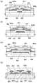
실시형태 3에서, 이 기술 등에 개시된 상기 표시 장치에 적용될 수 있는 트랜지스터의 일례가 기술될 것이다. 이 기술 등에 개시된 표시 장치에 적용될 수 있는 상기 트랜지스터의 구조에 관한 특정 제약은 없다; 예를 들면, 스태거형 또는 플래너형과 같은 톱-게이트 구조 또는 보텀-게이트 구조가 이용될 수 있다. 또한, 상기 트랜지스터는 하나의 채널 형성 영역을 포함하는 단일 게이트 구조, 2개의 채널 형성 영역들을 포함하는 이중 게이트 구조, 또는 3개의 채널 형성 영역들을 포함하는 삼중 게이트 구조를 가질 수 있다. 대안적으로, 상기 트랜지스터는 게이트 절연층을 사이에 제공하여 채널 영역 위 및 아래에 2개의 게이트 전극층들을 포함하는 듀얼 게이트 구조를 가질 수 있다. 도 8a 내지 도 8d에 도시된 트랜지스터의 단면 구조의 예들이 하기에 기술된다. 도 8a 내지 도 8d에 도시된 트랜지스터들은 반도체로서 산화물 반도체를 포함하는 트랜지스터들이다. 산화물 반도체는 높은 이동도 및 낮은 오프-상태 전류가 비교적 용이하게 저온 처리에서 얻어질 수 있는 이점을 제공한다; 그러나, 다른 반도체가 이용될 수 있음은 말할 필요가 없다.In Embodiment 3, an example of a transistor that can be applied to the display device disclosed in this technique or the like will be described. There are no particular constraints on the structure of the transistor that can be applied to the display device disclosed in this technique or the like; For example, a top-gate structure such as a staggered or planar type or a bottom-gate structure may be used. In addition, the transistor may have a single gate structure including one channel forming region, a double gate structure including two channel forming regions, or a triple gate structure including three channel forming regions. Alternatively, the transistor may have a dual gate structure including two gate electrode layers above and below the channel region by providing a gate insulating layer therebetween. Examples of the cross-sectional structures of the transistors shown in Figs. 8A to 8D are described below. The transistors shown in Figs. 8A to 8D are transistors including an oxide semiconductor as a semiconductor. Oxide semiconductors offer the advantage that high mobility and low off-state current can be obtained relatively easily in low temperature processing; However, it is needless to say that other semiconductors can be used.
도 8a에 도시된 트랜지스터(410)는 보텀 게이트형 트랜지스터의 종류이고, 또한 역 스태거형 트랜지스터라고 칭해진다.The
상기 트랜지스터(410)는 절연 표면을 가진 기판(400) 위에, 게이트 전극층(401), 게이트 절연층(402), 산화물 반도체층(403), 소스 전극층(405a), 및 드레인 전극층(405b)을 포함한다. 절연층(407)이 상기 트랜지스터(410)를 피복하도록 제공되고, 상기 산화물 반도체층(403) 위에 적층된다. 보호 절연층(409)이 상기 절연층(407) 위에 형성된다.The
도 8b에 도시된 트랜지스터(420)는 채널-보호형(채널-중지형)이라고 칭해지는 보텀-게이트형 구조의 종류이고, 또한 역 스태거형 트랜지스터라고 칭해진다.The
상기 트랜지스터(420)는, 절연 표면을 가진 기판(400) 위에, 게이트 전극층(401), 게이트 절연층(402), 산화물 반도체층(403), 상기 산화물 반도체층(403)의 채널 형성 영역을 피복하는 채널 보호층으로 기능하는 절연층(427), 소스 전극층(405a), 및 드레인 전극층(405b)을 포함한다. 보호 절연층(409)이 상기 트랜지스터(420)를 피복하도록 제공된다.The
도 8c에 도시된 트랜지스터(430)는 보텀-게이트형 트랜지스터이고, 절연 표면을 가진 기판(400) 위에, 게이트 전극층(401), 게이트 절연층(402), 소스 전극층(405a), 드레인 전극층(405b), 및 산화물 반도체층(403)을 포함한다. 절연층(407)이 상기 트랜지스터(430)를 피복하도록 제공되고, 상기 산화물 반도체층(403)과 접한다. 보호 절연층(409)이 상기 절연층(407) 위에 형성된다.A
상기 트랜지스터(430)에서, 상기 게이트 절연층(402)은 상기 기판(400) 및 상기 게이트 전극층(401) 상에 이들과 접하여 제공되고, 상기 소스 전극층(405a) 및 상기 드레인 전극층(405b)은 상기 게이트 절연층(402) 상에 이와 접하여 제공된다. 상기 산화물 반도체층(403)은 상기 게이트 절연층(402), 상기 소스 전극층(405a), 및 상기 드레인 전극층(405b) 위에 제공된다.In the
도 8d에 도시된 트랜지스터(440)는 톱-게이트형 트랜지스터의 종류이다. 상기 트랜지스터(440)는 절연 표면을 가진 기판(400) 위에, 절연층(437), 산화물 반도체층(403), 소스 전극층(405a), 드레인 전극층(405b), 게이트 절연층(402), 및 게이트 전극층(401)을 포함한다. 배선층(436a) 및 배선층(436b)이 상기 소스 전극층(405a) 및 상기 드레인 전극층(405b)에 각각 접하여 이와 전기적으로 접속되도록 제공된다.The
이 실시형태에서, 상술된 바와 같이, 상기 산화물 반도체층(403)은 반도체층으로 이용된다. 상기 산화물 반도체층(403)에 이용되는 산화물 반도체로서, 다음이 이용될 수 있다: 4원계 금속 산화물인 In-Sn-Ga-Zn-O-계 산화물 반도체; 3원계 금속 산화물인 In-Ga-Zn-O-계 산화물 반도체, In-Sn-Zn-O-계 산화물 반도체, In-Al-Zn-O-계 산화물 반도체, Sn-Ga-Zn-O-계 산화물 반도체, Al-Ga-Zn-O-계 산화물 반도체, 또는 Sn-Al-Zn-O-계 산화물 반도체; 2원계 금속 산화물인 In-Zn-O-계 산화물 반도체, Sn-Zn-O-계 산화물 반도체, Al-Zn-O-계 산화물 반도체, Zn-Mg-O-계 산화물 반도체, Sn-Mg-O-계 산화물 반도체, 또는 In-Mg-O-계 산화물 반도체; 또는 In-O-계 산화물 반도체, Sn-O-계 산화물 반도체, Zn-O-계 산화물 반도체 등. 산화 실리콘은 상기 산화물 반도체들 중 어느 것에 첨가될 수 있다. 상기 산화물 반도체층으로의 결정화를 저해하는 산화 실리콘의 첨가(SiOx (x > 0))는 제작 공정에서 상기 산화물 반도체층의 형성 후에 가열 처리가 수행될 때 상기 산화물 반도체층의 결정화를 억제할 수 있다. 이 실시형태에서, 예를 들면, 상기 In-Ga-Zn-O-계 산화물 반도체는 적어도 In, Ga, 및 Zn을 함유한 산화물을 의미하고, 상기 원소들의 조성비는 특별히 제한되지 않는다. 상기 In-Ga-Zn-O-계 산화물 반도체는 In, Ga, 및 Zn 이외의 원소를 함유할 수 있다.In this embodiment, as described above, the
상기 산화물 반도체층(403)으로서, InM03(ZnO)m(m > 0이고 m은 자연수가 아님)으로 표현된 박막이 이용될 수 있다. 이 실시형태에서, M은 Ga, Al, Mn, 및 Co로부터 선택된 하나 이상의 금속 원소들을 표현한다. 예를 들면, M은 Ga, Ga 및 Al, Ga 및 Mn, Ga 및 Co 등에 대응한다.The oxide as a semiconductor layer(403), InM0 3 (ZnO ) m has a thin film represented by (m> 0 and m is not a natural number) may be used. In this embodiment, M represents one or more metal elements selected from Ga, Al, Mn, and Co. For example, M corresponds to Ga, Ga and Al, Ga and Mn, Ga and Co, and the like.
상기 산화물 반도체층(403)을 포함하는 상기 트랜지스터들(410, 420, 430, 및 440)의 각각에서, 오프 상태의 전류(오프-상태 전류)가 작아질 수 있다. 따라서, 화상 데이터와 같은 전기 신호에 대한 유지 시간이 연장될 수 있고, 기록들 사이의 간격이 연장될 수 있다. 따라서, 리프레시 동작의 빈도가 감소될 수 있고, 이것은 전력 소비의 억제를 유발한다.In each of the
또한, 상기 산화물 반도체층(403)을 포함하는 상기 트랜지스터들(410, 420, 430, 및 440)에서, 비교적 높은 전계-효과 이동도가 얻어질 수 있고, 이것은 고속 동작을 가능하게 한다. 따라서, 상기 표시 장치의 화소부에서 상기 트랜지스터를 이용함으로써, 색 분리가 억제될 수 있고, 고품질 화상이 표시될 수 있다. 상기 트랜지스터들이 회로부 및 화소부에서 하나의 기판 위에 별도로 형성될 수 있기 때문에, 부품들의 수가 액정 표시 장치에서 감소될 수 있다.In addition, in the
절연 표면을 가진 상기 기판(400)에 이용되는 기판에 관한 특정 제약은 없지만, 바륨 보로실리케이트 유리, 알루미노보로실리케이트 유리 등의 유리 기판이 이용된다.There are no particular restrictions on the substrate used for the
상기 보텀-게이트 트랜지스터들(410, 420, 및 430)에서, 하지막의 역할을 하는 절연막이 상기 기판과 상기 게이트 전극층 사이에 제공될 수 있다. 상기 하지막은 상기 기판으로부터 불순물 원소의 확산을 방지하고, 질화 실리콘막, 산화 실리콘막, 질화산화 실리콘막, 및 산화질화 실리콘막 중 하나 이상을 이용하여 단층 구조 또는 적층 구조를 가지도록 형성될 수 있다.In the
상기 게이트 전극층(401)은 몰리브덴, 티타늄, 크롬, 탄탈, 텅스텐, 알루미늄, 구리, 네오디뮴, 또는 스칸듐과 같은 금속 재료, 또는 이들 재료들 중 어느 것을 주성분으로 함유한 합금 재료를 이용하여 단층 구조 또는 적층 구조를 가지도록 형성될 수 있다.The
상기 게이트 절연층(402)은 산화 실리콘층, 질화 실리콘층, 산화질화 실리콘층, 질화산화 실리콘층, 산화 알루미늄층, 질화 알루미늄층, 산화질화 알루미늄층, 질화산화 알루미늄층, 및 산화 하프늄층 중 하나 이상을 이용하여 플라즈마 CVD법, 스퍼터링법 등에 의해 단층 구조 또는 적층 구조를 가지도록 형성될 수 있다. 예를 들면, 플라즈마 CVD법에 의해, 50nm 이상 200nm 이하의 두께를 가진 질화 실리콘층(SiNy(y > 0))이 제 1 게이트 절연층으로 형성되고, 5nm 이상 300nm 이하의 두께를 가진 산화 실리콘층(SiOx(x > 0))이 상기 제 1 게이트 절연층 위에 제 2 게이트 절연층으로 형성되어, 200nm의 총 두께를 가진 게이트 절연층이 형성된다.The
상기 소스 전극층(405a) 및 상기 드레인 전극층(405b)에 이용되는 도전막으로서, 예를 들면, Al, Cr, Cu, Ta, Ti, Mo, 및 W로부터 선택된 원소막, 이들 원소들 중 어느 것을 성분으로 함유한 합금막, 이들 원소들을 조합하여 함유한 합금막 등이 이용될 수 있다. 대안적으로, Ti, Mo, W 등의 고융점 금속층이 Al, Cu 등의 금속층 위에 및/또는 아래에 적층되는 구조가 이용될 수 있다. 또한, Al막에서 힐록 또는 위스커의 발생을 방지하는 원소(Si, Nd, Sc 등)가 첨가되는 Al 재료를 이용하여 내열성이 개선될 수 있다.As the conductive film used for the
상기 소스 전극층(405a) 및 상기 드레인 전극층(405b)의 재료와 유사한 재료가 상기 소스 전극층(405a) 및 상기 드레인 전극층(405b)에 각각 접속된 상기 배선층(436a) 및 상기 배선층(436b)과 같은 도전막에 이용될 수 있다.A material similar to the material of the
대안적으로, 상기 소스 전극층(405a) 및 상기 드레인 전극층(405b)(상기 소스 전극층(405a) 및 상기 드레인 전극층(405b)과 동일한 층을 이용하여 형성된 배선을 포함)의 역할을 하는 상기 도전막은 도전성 금속 산화물을 이용하여 형성될 수 있다. 상기 도전성 금속 산화물로서, 산화 인듐(In2O3), 산화 주석(SnO2), 산화 아연(ZnO), 산화 인듐-산화 주석 합금(In2O3-SnO2, ITO로 약기함), 산화 인듐-산화 아연 합금(In2O3-ZnO), 또는 산화 실리콘이 함유된 이들 금속 재료들 중 어느 것이 이용될 수 있다.Alternatively, the conductive film serving as the
상기 절연층들(407, 427, 및 437)로서, 통상적으로, 산화 실리콘막, 산화질화 실리콘막, 산화 알루미늄막, 또는 산화질화 알루미늄막과 같은 무기 절연막이 이용될 수 있다.As the insulating
상기 보호 절연층(409)으로서, 질화 실리콘막, 질화 알루미늄막, 질화산화 실리콘막, 또는 질화산화 알루미늄막이 이용될 수 있다.As the protective insulating
트랜지스터로 인한 표면 거칠기를 감소시키기 위해 평탄화 절연막이 상기 보호 절연층(409) 위에 형성될 수 있다. 상기 평탄화 절연막으로서, 폴리이미드, 아크릴, 또는 벤조사이클로부텐과 같은 유기 재료가 이용될 수 있다. 이러한 유기 재료들과 마찬가지로, 저유전률 재료(low-k 재료) 등을 이용하는 것이 가능하다. 상기 평탄화 절연막은 이들 재료들로부터 형성된 복수의 절연막들을 적층하여 형성될 수 있다.A planarization insulating film may be formed on the protective insulating
따라서, 이 실시형태에서, 산화물 반도체층을 포함하는 트랜지스터를 이용함으로써, 고성능 표시 장치가 제공될 수 있다.Therefore, in this embodiment, by using the transistor including the oxide semiconductor layer, a high-performance display device can be provided.
오프-상태 전류가 감소되고 산화물 반도체층을 포함하는 상기 트랜지스터로, 상기 트랜지스터 및 상기 용량 소자에 접속되는 상기 표시 소자에 저장된 전하는 상기 오프-상태의 트랜지스터를 통해 그다지 누설되지 않고, 상기 트랜지스터가 오프 상태가 되기 전에 기록된 상기 데이터가 장시간 동안 유지될 수 있다.State transistor, wherein the off-state current is reduced and the transistor including the oxide semiconductor layer, the charge stored in the display element connected to the transistor and the capacitor element does not leak much through the off-state transistor, The recorded data can be maintained for a long time.
(실시형태 4)(Fourth Embodiment)
실시형태 4에서, 산화물 반도체층을 포함하는 트랜지스터의 예, 및 그 제작 방법의 예가 도 9a 내지 도 9e를 이용하여 상세히 기술될 것이다. 상기 실시형태들은 상기 실시형태들에서와 동일한 부분들 또는 유사한 기능들을 가진 부분들 또는 단계들에 적용될 수 있고, 반복 기술은 생략된다.In Embodiment 4, an example of a transistor including an oxide semiconductor layer and an example of a manufacturing method thereof will be described in detail with reference to Figs. 9A to 9E. The embodiments may be applied to parts or steps having the same parts or similar functions as those in the above embodiments, and the repetition description is omitted.
도 9a 내지 도 9e는 트랜지스터의 단면 구조예를 도시한다. 도 9a 내지 도 9e에 도시된 트랜지스터(510)는 도 8a에 도시된 상기 트랜지스터(410)와 유사한 보텀-게이트 역-스태거형 트랜지스터이다.9A to 9E show examples of the cross-sectional structure of the transistor. The
이 실시형태에서 반도체층에 이용된 산화물 반도체는 i형(진성) 산화물 반도체 또는 실질적으로 i형(진성) 산화물 반도체이고, 이것은 n형 불순물인 수소가 산화물 반도체로부터 제거되는 방식으로 획득되고, 상기 산화물 반도체는 상기 산화물 반도체의 주성분들이 아닌 불순물들을 가능한 적게 함유하도록 고순도화된다. 즉, 본 발명에 따른 상기 산화물 반도체는 불순물의 첨가에 의해서가 아니라 수소 또는 수분과 같은 불순물의 가능한 많은 제거에 의해 고순도화에 의해 i형(진성) 반도체가 되거나 또는 그에 근접하게 되는 특징이 있다. 따라서, 상기 트랜지스터(510)에 포함된 상기 산화물 반도체층은 고순도화되고 전기적으로 i형(진성)이 되는 산화물 반도체층이다.In this embodiment, the oxide semiconductor used for the semiconductor layer is an i-type (intrinsic) oxide semiconductor or a substantially i-type (intrinsic) oxide semiconductor, which is obtained in such a manner that hydrogen as an n-type impurity is removed from the oxide semiconductor, The semiconductor is highly purified so as to contain as few impurities as possible than the main components of the oxide semiconductor. That is, the oxide semiconductor according to the present invention is characterized not only by the addition of impurities, but also by iodine (intrinsic) semiconductors due to high purity by as much as possible removal of impurities such as hydrogen or moisture, or to become close to them. Accordingly, the oxide semiconductor layer included in the
상기 고순도화된 산화물 반도체에서의 캐리어들의 수가 매우 작고(0에 근접함), 상기 캐리어 농도는 1 × 10¹⁴/cm3 미만, 바람직하게 1 × 10¹²/cm3 미만, 더욱 바람직하게 1 × 10¹¹/cm3 미만이다.The number of carriers in the high-purity oxide semiconductor is very small (approaching 0), the carrier concentration is less than 1 x 10¹⁴ / cm3 , preferably less than 1 x 10¹² / cm3 ,11 / cm <3 & gt ;.
상기 산화물 반도체층에서의 상기 캐리어들의 수가 극히 작기 때문에, 상기 트랜지스터의 오프-상태 전류가 감소될 수 있다. 오프-상태 전류량이 적을수록 양호하다.Since the number of carriers in the oxide semiconductor layer is extremely small, the off-state current of the transistor can be reduced. The smaller the off-state current amount is, the better.
특히, 상기 산화물 반도체층을 포함하는 상기 트랜지스터에서, 실온에서의 채널 폭에서 마이크로미터 당 오프-상태 전류 밀도가 10aA/㎛(1 × 10-17A/㎛) 이하, 바람직하게는 1aA/㎛(1 × 10-18A/㎛) 이하, 더욱 바람직하게는 10zA/㎛(1 × 10-20A/㎛) 이하일 수 있다.Particularly, in the transistor including the oxide semiconductor layer, the off-state current density per micrometer in the channel width at room temperature is 10 A / μm (1 × 10-17 A / μm) or less, preferably 1 A / 1 × 10-18 A / ㎛) is less, and more preferably may be less than10zA / ㎛ (1 × 10 -20 A / ㎛).
실시형태 2의 상기 화소부에서의 트랜지스터로서 이용되는 오프-상태에서의 전류값(오프-상태-전류값)이 매우 적은 상기 트랜지스터로, 정지 화상 영역에서의 리프레시 동작은 화상 데이터의 적은 기록 횟수로 수행될 수 있다.(The off-state-current value) in the off-state, which is used as the transistor in the pixel portion of the embodiment 2, the refresh operation in the still image area is performed with a small number of times of recording of the image data .
또한, 상기 산화물 반도체층을 포함하는 상기 트랜지스터(510)에서, 온-상태 전류의 온도 의존성이 거의 관찰되지 않고, 오프-상태 전류가 극히 적게 남아있다.Further, in the
기판(505) 위의 상기 트랜지스터(510)를 제작하는 단계들이 도 9a 내지 도 9e를 이용하여 하기에 기술된다.The steps of fabricating the
먼저, 절연 표면을 가진 상기 기판(505) 위에 도전막이 형성되고, 그 후에 제 1 포토리소그래피 단계가 수행되어, 게이트 전극층(511)이 형성된다. 레지스트 마스크가 잉크젯법에 의해 형성될 수 있다. 잉크젯법에 의한 상기 레지스트 마스크의 형성은 포토마스크를 필요로 하지 않는다; 따라서, 제작 비용이 감소될 수 있다.First, a conductive film is formed on the
절연 표면을 가진 상기 기판(505)으로서, 실시형태 3에 기술된 상기 기판(400)과 유사한 기판이 이용될 수 있다. 이 실시형태에서, 유리 기판이 상기 기판(505)으로서 이용된다.As the
하지막의 역할을 하는 절연막이 상기 기판(505)과 상기 게이트 전극층(511) 사이에 제공될 수 있다. 상기 하지막은 상기 기판(505)으로부터 불순물 원소의 확산을 방지하고, 질화 실리콘막, 산화 실리콘막, 질화산화 실리콘막, 및 산화질화 실리콘막 중 하나 이상을 이용하여 단층 구조 또는 적층 구조를 가지도록 형성될 수 있다.An insulating film serving as a base film may be provided between the
또한, 상기 게이트 전극층(511)은 몰리브덴, 티타늄, 탄탈, 텅스텐, 알루미늄, 구리, 네오디뮴, 또는 스칸듐과 같은 금속 재료, 또는 이들 재료들 중 어느 것을 주성분으로 함유한 합금 재료를 이용하여 단층 구조 또는 적층 구조를 가지도록 형성될 수 있다.The
다음에, 게이트 절연층(507)이 상기 게이트 전극층(511) 위에 형성된다. 상기 게이트 절연층(507)은 산화 실리콘층, 질화 실리콘층, 산화질화 실리콘층, 질화산화 실리콘층, 산화 알루미늄층, 질화 알루미늄층, 산화질화 알루미늄층, 질화산화 알루미늄층, 및 산화 하프늄층 중 하나 이상을 이용하여 플라즈마 CVD법, 스퍼터링법 등에 의해 단층 구조 또는 적층 구조를 가지도록 형성될 수 있다.Next, a
이 실시형태에서의 상기 산화물 반도체로서, 불순물들을 제거하여 만들어지는 i형 또는 실질적으로 i형 산화물 반도체가 이용된다. 이러한 고순도화된 산화물 반도체는 계면 상태 및 계면 전하에 매우 민감하다; 따라서, 상기 산화물 반도체층과 상기 게이트 절연층 사이의 계면이 중요하다. 그러한 이유로, 상기 고순도화된 산화물 반도체와 접하는 상기 게이트 절연층이 고품질을 가져야 한다.As the oxide semiconductor in this embodiment, an i-type or substantially i-type oxide semiconductor made by removing impurities is used. Such high purity oxide semiconductors are very sensitive to interfacial states and interface charge; Therefore, the interface between the oxide semiconductor layer and the gate insulating layer is important. For this reason, the gate insulating layer in contact with the high-purity oxide semiconductor must have high quality.
예를 들면, 절연층이 조밀하게 형성될 수 있고 높은 내전압 및 고품질을 가지기 때문에, 마이크로파들(예를 들면, 2.45GHz의 주파수)을 이용한 고밀도 플라즈마 CVD법이 채택되는 것이 바람직하다. 이것은 상기 고순도화된 산화물 반도체 및 상기 고품질 게이트 절연층이 서로 근접하게 접하기 때문이고, 그에 의해 높은 계면 특성들을 제공하기 위해 계면 상태 밀도가 감소될 수 있다.For example, a high-density plasma CVD method using microwaves (for example, a frequency of 2.45 GHz) is preferably adopted because the insulating layer can be formed densely and has high withstand voltage and high quality. This is because the high-purity oxide semiconductor and the high-quality gate insulating layer are in close contact with each other, whereby the interface state density can be reduced to provide high interface characteristics.
말할 필요도 없이, 스퍼터링법 또는 플라즈마 CVD법과 같은 다른 성막 방법이 게이트 절연층으로서 고품질 절연층의 형성을 가능하게 하는 한 상기 방법이 채용될 수 있다. 대안적으로, 또는 부가적으로, 상기 절연층과 산화물 반도체 사이의 상기 계면의 막 품질 및 특성이 상기 절연층의 형성 후에 수행되는 가열 처리에 의해 개선되는 절연층이 게이트 절연층으로서 이용될 수 있다. 어떠한 경우든, 절연층이 산화물 반도체와의 상기 계면의 계면 상태 밀도를 감소시킬 수 있고 게이트 절연층으로서 높은 막 품질을 가지는 것 외에도 양호한 계면을 형성할 수 있는 한 임의의 절연층이 이용될 수 있다.Needless to say, the above method can be employed as long as other film forming methods such as the sputtering method or the plasma CVD method can form a high-quality insulating layer as the gate insulating layer. Alternatively or additionally, an insulating layer may be used as the gate insulating layer, wherein the film quality and characteristics of the interface between the insulating layer and the oxide semiconductor are improved by a heat treatment performed after formation of the insulating layer . In any case, any insulating layer can be used so long as the insulating layer can reduce the interface state density of the interface with the oxide semiconductor and can form a good interface in addition to having a high film quality as the gate insulating layer .
또한, 수소, 수산기, 및 습기가 상기 게이트 절연층(507) 및 산화물 반도체막(530)에 가능한 적게 함유될 수 있기 위해, 상기 기판(505)에 흡착된 수소 및 습기와 같은 불순물들이 제거되고 배기가 수행되도록, 상기 게이트 전극층(511)이 구비된 상기 기판(505) 또는 상기 게이트 절연층(507)까지 이를 포함하는 소자들이 구비된 상기 기판(505)은 상기 산화물 반도체막(530)의 성막을 위한 전처리로서 스퍼터링 장치의 예비 가열실에서 예비 가열되는 것이 바람직하다. 상기 예비 가열실에 제공된 배기 수단으로서, 크라이오펌프가 바람직하다. 이 예비 가열 처리는 반드시 수행될 필요는 없다. 이 예비 가열 처리는 절연층(516)을 성막하기 전에 소스 전극층(515a) 및 드레인 전극층(515b)까지 이를 포함하는 소자들이 구비된 상기 기판(505)에 대해 유사하게 수행될 수 있다.In addition, since hydrogen, hydroxyl, and moisture can be contained as little as possible in the
다음에, 2nm 이상 200nm 이하, 바람직하게 5nm 이상 30nm 이하의 두께를 가진 상기 산화물 반도체막(530)이 상기 게이트 절연층(507) 위에 형성된다(도 9a 참조).Next, the
상기 산화물 반도체막(530)이 스퍼터링법에 의해 형성되기 전에, 상기 게이트 절연층(507)의 표면 상에 부착된 가루 물질들(또한 입자들 또는 먼지라고 칭해짐)은 아르곤 가스가 도입되고 플라즈마가 생성되는 역 스퍼터링에 의해 제거되는 것이 바람직함을 유념한다. 상기 역 스퍼터링은 타겟측에 대한 전압의 인가 없이, RF 전원이 표면을 개질하기 위해 아르곤 분위기에서 기판측에 대한 전압의 인가를 위해 이용되는 방법을 나타낸다. 아르곤 분위기 대신에, 질소 분위기, 헬륨 분위기, 산소 분위기 등이 이용될 수 있다.Before the
상기 산화물 반도체막(530)에 이용되는 산화물 반도체로서, 4원계 금속 산화물, 3원계 금속 산화물, 2원계 금속 산화물, In-O-계 산화물 반도체, Sn-O-계 산화물 반도체, 또는 Zn-O-계 산화물 반도체와 같은 실시형태 3에 기술된 임의의 산화물 반도체가 이용될 수 있다. 또한, SiO2는 상기 산화물 반도체에 함유될 수 있다. 이 실시형태에서, 상기 산화물 반도체막(530)은 In-Ga-Zn-O-계 산화물 반도체 타겟을 이용하여 스퍼터링법에 의해 성막된다. 이 단계에서의 단면도는 도 9a이다. 상기 산화물 반도체막(530)은 희가스(통상적으로, 아르곤) 분위기, 산소 분위기, 또는 희가스와 산소의 혼합 분위기에서 스퍼터링법에 의해 형성될 수 있다.A ternary metal oxide, a ternary metal oxide, a binary metal oxide, an In-O-based oxide semiconductor, a Sn-O-based oxide semiconductor, or a Zn-O- Any of the oxide semiconductors described in Embodiment Mode 3, such as a system oxide semiconductor, may be used. Further, SiO2 can be contained in the oxide semiconductor. In this embodiment, the
스퍼터링법에 의해 상기 산화물 반도체막(530)을 성막하기 위한 타겟으로서, 예를 들면, In2O3 : Ga2O3 : ZnO = 1 : 1 : 1 [mol %] (즉, In : Ga : Zn = 1 : 1 : 0.5 [atom %]) 등의 조성비를 가진 타겟이 이용될 수 있다. 대안적으로, In : Ga : Zn = 1 : 1 : 1 [atom %] 또는 In : Ga : Zn = 1 : 1 : 2 [atom %]의 조성비를 가진 타겟이 이용될 수 있다. 상기 금속 산화물 타겟의 충전률은 90% 이상 100% 이하, 바람직하게 95% 이상 99.9% 이하이다. 높은 충전률을 가진 금속 산화물 타겟을 이용하여, 상기 성막된 산화물 반도체막은 고밀도를 가진다.For example, In2 O3 : Ga2 O3 : ZnO = 1: 1: 1 [mol%] (that is, In: Ga: Zn = 1: 1: 0.5 [atom%]) may be used. Alternatively, a target having a composition ratio of In: Ga: Zn = 1: 1: 1 [atom%] or In: Ga: Zn = 1: 1: 2 [atom%] may be used. The filling rate of the metal oxide target is 90% or more and 100% or less, preferably 95% or more and 99.9% or less. Using the metal oxide target having a high filling factor, the deposited oxide semiconductor film has high density.
수소, 수분, 수산기, 또는 수소화물과 같은 불순물이 제거되는 고순도 가스가 상기 산화물 반도체막(530)의 성막을 위해 상기 스퍼터링 가스로서 이용되는 것이 바람직하다.It is preferable that a high purity gas from which impurities such as hydrogen, moisture, hydroxyl groups, or hydrides are removed is used as the sputtering gas for forming the
상기 기판은 감압 하의 성막실에 배치되고, 기판 온도는 100℃ 이상 600℃ 이하, 바람직하게 200℃ 이상 400℃ 이하의 온도로 설정된다. 상기 기판이 가열되는 동안 상기 산화물 반도체막을 성막함으로써, 상기 산화물 반도체막에 포함된 불순물들의 농도가 감소될 수 있다. 또한, 스퍼터링에 의한 손상이 감소될 수 있다. 그 후에, 상기 성막실 내의 잔여 습기가 제거되고, 수소 및 습기가 제거되는 스퍼터링 가스가 도입되고, 상술된 타겟이 이용되어, 상기 산화물 반도체막(530)이 상기 기판(505) 위에 형성된다. 상기 성막실 내의 상기 잔여 습기를 제거하기 위해, 흡착형 진공 펌프, 예를 들면, 크라이오펌프, 이온 펌프, 또는 티타늄 서브리메이션 펌프(titanium sublimation pump)가 이용되는 것이 바람직하다. 상기 배기 수단은 콜드 트랩이 구비된 터보 펌프일 수 있다. 상기 크라이오펌프로 배기되는 상기 성막실에서, 수소 원자, 물(H2O)과 같은 수소 원자를 함유한 화합물(더욱 바람직하게, 또한 탄소 원자를 함유한 화합물) 등이 제거되고, 그에 의해 상기 성막실에서 성막된 상기 산화물 반도체막에서의 불순물의 농도가 감소될 수 있다.The substrate is placed in a deposition chamber under a reduced pressure, and the substrate temperature is set to a temperature of 100 ° C or more and 600 ° C or less, preferably 200 ° C or more and 400 ° C or less. By forming the oxide semiconductor film while the substrate is heated, the concentration of the impurities contained in the oxide semiconductor film can be reduced. In addition, damage due to sputtering can be reduced. Thereafter, the residual moisture in the deposition chamber is removed, a sputtering gas for removing hydrogen and moisture is introduced, and the above-described target is used so that the
상기 성막 조건의 일례로서, 상기 기판과 상기 타겟 사이의 거리는 100mm이고, 압력은 0.6Pa이고, 직류(DC) 전력은 0.5kW이고, 분위기는 산소 분위기(산소 유량비가 100%임)이다. 상기 성막시 생성된 가루 물질들(또한 입자들 또는 먼지라고 칭해짐)이 감소될 수 있고 막 두께가 균일해질 수 있기 때문에, 펄스 직류 전원을 이용하는 것이 바람직하다.As an example of the film forming conditions, the distance between the substrate and the target is 100 mm, the pressure is 0.6 Pa, the direct current (DC) power is 0.5 kW, and the atmosphere is an oxygen atmosphere (oxygen flow ratio is 100%). It is preferable to use a pulsed direct current power source because the powdery materials (also referred to as particles or dust) generated during the film formation can be reduced and the film thickness can be made uniform.
다음에, 상기 산화물 반도체막(530)이 제 2 포토리소그래피 단계에 의해 섬형 산화물 반도체층으로 가공된다. 상기 섬형 산화물 반도체층을 형성하기 위한 레지스트 마스크가 잉크젯법에 의해 형성될 수 있다. 잉크젯법에 의한 상기 레지스트 마스크의 형성은 포토마스크를 필요로 하지 않는다; 따라서, 제작 비용이 감소될 수 있다.Next, the
콘택트 홀이 상기 게이트 절연층(507)에 형성되는 경우에, 상기 콘택트 홀을 형성하는 단계는 상기 산화물 반도체막(530)의 가공과 동시에 수행될 수 있다.In the case where a contact hole is formed in the
이 실시형태에서 상기 산화물 반도체막(530)의 에칭을 위해, 습식 에칭 및 건식 에칭 중 하나 또는 둘다가 이용될 수 있다. 상기 산화물 반도체막(530)의 습식 에칭을 위해 이용된 에천트로서, 예를 들면, 인산, 아세트산, 및 질산의 혼합 용액 등이 이용될 수 있다. ITO07N(KANTO CHEMICAL CO., INC.에 의해 생산됨)이 마찬가지로 이용될 수 있다.In this embodiment, for etching the
다음에, 상기 산화물 반도체층이 제 1 가열 처리된다. 상기 산화물 반도체층은 이 제 1 가열 처리에 의해 탈수화 또는 탈수소화될 수 있다. 상기 제 1 가열 처리의 온도는 400℃ 이상 750℃ 이하, 또는 400℃ 이상 상기 기판의 변형점 이하이다. 이 실시형태에서, 상기 기판은 가열 처리 장치의 일종인 전기로에 넣어지고, 질소 분위기에서 1시간 동안 450℃에서 상기 산화물 반도체층에 대한 가열 처리가 수행된 다음, 상기 산화물 반도체층은 수분 또는 수소가 상기 산화물 반도체층에 혼입되는 것이 방지되도록 대기에 노출되는 것이 방지된다; 이러한 방식으로, 산화물 반도체층(531)이 획득된다(도 9b 참조).Next, the oxide semiconductor layer is subjected to the first heat treatment. The oxide semiconductor layer may be dehydrated or dehydrogenated by the first heat treatment. The temperature of the first heat treatment is not less than 400 ° C and not more than 750 ° C, or not more than 400 ° C not more than the strain points of the substrate. In this embodiment, the substrate is placed in an electric furnace which is a kind of a heat treatment apparatus, and a heat treatment is performed on the oxide semiconductor layer at 450 DEG C for one hour in a nitrogen atmosphere, Is prevented from being exposed to the atmosphere so as to be prevented from being mixed into the oxide semiconductor layer; In this manner, an
상기 가열 처리 장치는 전기로에 제한되지 않고, 저항 발열체와 같이 가열 소자로부터 열전도 또는 열복사에 의해 대상을 가열하기 위한 장치를 가질 수 있다. 예를 들면, GRTA(gas rapid thermal anneal) 장치 또는 LRTA(lamp rapid thermal anneal) 장치와 같은 RTA(rapid thermal anneal) 장치가 이용될 수 있다. LRTA 장치는 할로겐 램프, 금속 할로겐화물 램프, 크세논 아크 램프, 카본 아크 램프, 고압 나트륨 램프는 고압 수은 램프와 같은 램프로부터 방출된 광(전자파)의 복사에 의해 대상을 가열하기 위한 장치이다. GRTA 장치는 고온 가스를 이용하는 가열 처리를 위한 장치이다. 상기 고온 가스로서, 질소 또는 아르곤과 같은 희가스 등과 같은 가열 처리에 의해 대상과 반응하지 않는 불활성 가스가 이용된다.The heat treatment apparatus is not limited to an electric furnace but may have a device for heating an object by heat conduction or thermal radiation from a heating element such as a resistance heating element. For example, a rapid thermal anneal (RTA) device such as a gas rapid thermal annealing (GRTA) device or a lamp rapid thermal annealing (LRTA) device may be used. The LRTA device is a device for heating a target by radiation of light (electromagnetic waves) emitted from a lamp such as a halogen lamp, a metal halide lamp, a xenon arc lamp, a carbon arc lamp, and a high pressure sodium lamp. The GRTA apparatus is a device for heat treatment using a hot gas. As the high-temperature gas, inert gas that does not react with the object by heat treatment such as nitrogen or rare gas such as argon is used.
예를 들면, 상기 제 1 가열 처리로서, 상기 기판이 650℃ 내지 700℃ 정도의 온도로 가열된 불활성 가스로 이동되고, 수분 동안 가열되고, 고온으로 가열된 상기 불활성 가스로부터 이동되는 GRTA가 수행될 수 있다.For example, as the first heat treatment, the substrate is moved to an inert gas heated to a temperature of about 650 DEG C to 700 DEG C, heated for a few minutes, and moved from the inert gas heated to a high temperature, .
상기 제 1 가열 처리에서, 수분, 수소 등은 질소 또는 헬륨, 네온, 또는 아르곤과 같은 희가스의 분위기에 함유되지 않는 것이 바람직하다. 가열 처리 장치에 도입되는 질소 또는 헬륨, 네온, 또는 아르곤과 같은 상기 희가스의 순도는 6N(99.9999 %) 이상, 더욱 바람직하게 7N(99.99999 %) 이상으로 설정되는 것이 바람직하다(즉, 상기 불순물 농도는 1ppm 이하가 바람직하고 0.1ppm 이하가 더욱 바람직하다).In the first heat treatment, moisture, hydrogen, and the like are preferably not contained in an atmosphere of rare gas such as nitrogen or helium, neon, or argon. It is preferable that the purity of the rare gas introduced into the heat treatment apparatus such as nitrogen or helium, neon or argon is set to 6N (99.9999%) or more, more preferably 7N (99.99999% More preferably 1 ppm or less, and even more preferably 0.1 ppm or less).
또한, 상기 산화물 반도체층이 상기 제 1 가열 처리에서 가열된 후에, 고순도 산소 가스, 고순도 N2O 가스, 또는 초건조 공기(이슬점이 -40℃ 이하이고, 바람직하게는 -60℃ 이하임)는 동일 노에 도입될 수 있다. 수분, 수소 등이 상기 산소 가스 또는 N2O 가스에 함유되지 않는 것이 바람직하다. 상기 가열 처리 장치에 도입되는 상기 산소 가스 또는 상기 N2O 가스의 순도는 6N 이상, 더욱 바람직하게 7N 이상이 바람직하다(즉, 상기 산소 가스 또는 상기 N2O 가스의 불순물 농도는 1ppm 이하가 바람직하고 0.1ppm 이하가 더욱 바람직하다). 상기 산소 가스 또는 상기 N2O 가스는 상기 산화물 반도체의 주성분인 산소를 공급하도록 작용하고 탈수화 또는 탈수소화에 의해 불순물들을 제거하는 단계에 의해 감소되어, 상기 산화물 반도체층은 고순도화 및 전기적으로 i형(진성) 산화물 반도체가 되게 된다.Further, after the oxide semiconductor layer is heated in the first heat treatment, a high-purity oxygen gas, a high-purity N2 O gas, or super-dry air (the dew point is -40 ° C or lower, preferably -60 ° C or lower) Can be introduced into the same furnace. Moisture, hydrogen or the like is not contained in the oxygen gas or the N2 O gas. The purity of the oxygen gas or the N2 O gas introduced into the heat treatment apparatus is preferably 6N or more, more preferably 7N or more (that is, the impurity concentration of the oxygen gas or the N2 O gas is preferably 1 ppm or less And more preferably 0.1 ppm or less). The oxygen gas or the N2 O gas is reduced by the step of acting to supply oxygen which is a main component of the oxide semiconductor and removing impurities by dehydration or dehydrogenation so that the oxide semiconductor layer is highly purified and electrically Type (intrinsic) oxide semiconductor.
상기 산화물 반도체층의 상기 제 1 가열 처리는 상기 섬형 산화물 반도체층으로 가공되기 전에 상기 산화물 반도체막(530)에 대해 수행될 수 있다. 그 경우, 상기 기판은 상기 제 1 가열 처리 후에 상기 가열 장치로부터 꺼내어지고, 그 후에 그것에 대해 포토리소그래피 단계가 수행된다.The first heat treatment of the oxide semiconductor layer may be performed on the
상기 제 1 가열 처리는 상기 산화물 반도체층의 성막 후라면, 상기 타이밍에 제한되지 않고 다음의 타이밍들 중 어느 것에서 수행될 수 있다: 소스 전극층 및 드레인 전극층이 상기 산화물 반도체층 위에 형성된 후; 절연층이 상기 소스 전극층 및 상기 드레인 전극층 위에 형성된 후.The first heat treatment may be performed at any one of the following timings after the formation of the oxide semiconductor layer, without being limited to the above timing: after the source electrode layer and the drain electrode layer are formed on the oxide semiconductor layer; After the insulating layer is formed on the source electrode layer and the drain electrode layer.
또한, 콘택트 홀이 상기 게이트 절연층(507)에서 형성되는 경우에, 상기 제 1 가열 처리가 상기 산화물 반도체막(530)에 대해 수행되기 전 또는 후에 상기 콘택트 홀을 형성하는 단계가 수행될 수 있다.Further, in the case where a contact hole is formed in the
또한, 상기 산화물 반도체층으로서, 상기 막의 표면에 수직인 c-축 배향된 결정 영역을 가진 산화물 반도체층이 하지 부재의 재료에 상관없이 2회의 성막 및 2회의 가열 처리를 수행하여 형성될 수 있다. 예를 들면, 3nm 이상 15nm 이하의 두께를 가진 제 1 산화물 반도체막이 성막되고, 제 1 가열 처리가 질소, 산소, 희가스, 또는 건조 대기 분위기에서 450℃ 이상 850℃ 이하, 바람직하게 550℃ 이상 750℃ 이하의 온도에서 수행되어, 표면을 포함하는 영역에 결정 영역(판형 결정)을 가진 제 1 산화물 반도체막이 형성된다. 그 후에, 상기 제 1 산화물 반도체막보다 두꺼운 두께를 가진 제 2 산화물 반도체막이 형성되고, 450℃ 이상 850℃ 이하, 바람직하게는 600℃ 이상 700℃ 이하의 온도에서 제 2 가열 처리가 수행되어, 결정 성장이 상기 결정 성장의 시드로서 상기 제 1 산화물 반도체막을 이용하여 상향으로 진행하고, 전체의 제 2 산화물 반도체막이 결정화된다. 이러한 방식으로, 두꺼운 두께를 가진 결정 영역을 가진 상기 산화물 반도체층이 형성될 수 있다.Further, as the oxide semiconductor layer, an oxide semiconductor layer having a crystal region oriented in the c-axis perpendicular to the surface of the film can be formed by performing the film formation twice and the heat treatment twice, irrespective of the material of the base member. For example, a first oxide semiconductor film having a thickness of 3 nm or more and 15 nm or less is formed, and the first heat treatment is performed at 450 占 폚 or higher and 850 占 폚 or lower, preferably 550 占 폚 or higher and 750 占 폚 (A plate-like crystal) in the region including the surface is formed. Thereafter, a second oxide semiconductor film having a thickness larger than that of the first oxide semiconductor film is formed, and a second heat treatment is performed at a temperature of 450 캜 or higher and 850 캜 or lower, preferably 600 캜 or higher and 700 캜 or lower, The growth progresses upward by using the first oxide semiconductor film as a seed of crystal growth, and the entire second oxide semiconductor film is crystallized. In this way, the oxide semiconductor layer having a crystal region with a large thickness can be formed.
다음에, 상기 소스 및 드레인 전극층들(상기 소스 및 드레인 전극층들과 동일한 층으로 형성된 배선을 포함)의 역할을 하는 도전막이 상기 게이트 절연층(507) 및 상기 산화물 반도체층(531) 위에 형성된다. 상기 소스 및 드레인 전극층들의 역할을 하는 상기 도전막으로서, 실시형태 3에 기술된 상기 소스 전극층(405a) 및 상기 드레인 전극층(405b)에 이용되는 재료가 이용될 수 있다.Next, a conductive film serving as the source and drain electrode layers (including wirings formed of the same layer as the source and drain electrode layers) is formed on the
제 3 포토리소그래피 단계에 의해 상기 도전막 위에 레지스트 마스크가 형성되고, 상기 소스 전극층(515a) 및 상기 드레인 전극층(515b)을 형성하기 위해 선택적으로 에칭된 다음, 상기 레지스트 마스크가 제거된다(도 9c 참조).A resist mask is formed on the conductive film by a third photolithography step and is selectively etched to form the
상기 제 3 포토리소그래피 단계에서 상기 레지스트 마스크의 형성시의 노광은 자외선, KrF 레이저 광, 또는 ArF 레이저 광을 이용하여 수행될 수 있다. 트랜지스터의 채널 길이 L이 상기 소스 전극층 및 상기 드레인 전극층의 하단부들 사이의 피치에 의해 결정되고, 이것은 상기 산화물 반도체층(531) 위에 서로 인접한다. 노광이 25nm 미만의 채널 길이 L에 대해 수행되는 경우, 상기 제 3 포토리소그래피 단계에서의 상기 레지스트 마스크의 형성시의 상기 노광은 수 나노미터 내지 수십 나노미터의 초단파장을 가진 초자외선을 이용하여 수행되는 것이 바람직하다. 초자외선에 의한 노광에서, 해상도가 높고 초점 심도가 크다. 따라서, 상기 트랜지스터의 채널 길이 L은 10nm 이상 1000nm 이하일 수 있고, 이것은 회로의 동작 속도를 증가시킬 수 있고, 상기 오프-상태 전류가 극히 작기 때문에, 전력 소비가 감소될 수 있다. 포토리소그래피 단계에서 이용된 포토마스크들의 수를 감소시키고 포토리소그래피 단계들의 수를 감소시키기 위해, 상기 에칭 단계는 복수의 강도들을 가지도록 광이 투과되는 포토마스크인 다계조 마스크를 이용하여 수행될 수 있다. 다계조 마스크를 이용하여 형성된 레지스트 마스크는 복수의 두께들을 가지고, 또한 에칭에 의해 형상이 변경될 수 있다; 따라서, 상기 레지스트 마스크는 상이한 패턴들로 가공하기 위한 복수의 에칭 단계들에서 이용될 수 있다. 따라서, 적어도 2 종류의 상이한 패턴들에 대응하는 레지스트 마스크는 하나의 다계조 마스크에 의해 형성될 수 있다. 따라서, 포토마스크들의 수가 감소될 수 있고, 포토리소그래피 단계들의 수가 따라서 감소될 수 있고, 이것은 제작 공정의 간략화를 가능하게 한다.The exposure in forming the resist mask in the third photolithography step may be performed using ultraviolet light, KrF laser light, or ArF laser light. The channel length L of the transistor is determined by the pitch between the source electrode layer and the lower end portions of the drain electrode layer and is adjacent to each other on the
상기 도전막이 에칭될 때, 상기 산화물 반도체층(531)을 에칭하지 않고 분할하지 않도록 에칭 조건들이 최적화되는 것이 바람직함을 유념한다. 그러나, 상기 도전막만 에칭되고 상기 산화물 반도체층(531)이 전혀 에칭되지 않는 에칭 조건들을 획득하는 것은 어렵다; 일부 경우들에서, 오목부가 되도록 상기 도전막의 에칭에 의해 상기 산화물 반도체층(531)의 일부만 에칭된다.It is noted that when the conductive film is etched, the etching conditions are preferably optimized such that the
이 실시형태에서, Ti막이 상기 도전막으로서 이용되고 상기 In-Ga-Zn-O-계 산화물 반도체가 상기 산화물 반도체층(531)으로서 이용되기 때문에, 상기 도전막을 에칭하기 위한 에천트로서 암모니아과수(암모니아, 물 및 과산화 수소수의 혼합 용액)가 이용된다.In this embodiment, since the Ti film is used as the conductive film and the In-Ga-Zn-O-based oxide semiconductor is used as the
다음에, N2O, N2, 또는 Ar을 이용한 플라즈마 처리는 상기 산화물 반도체층의 노출된 부분의 표면에 흡착되는 수분들을 제거하기 위해 수행될 수 있다. 상기 플라즈마 처리가 수행되는 경우에, 상기 절연층(516)은 상기 산화물 반도체층의 일부와 접하여 대기에 노출되지 않고 보호 절연막으로서 형성된다.Next, a plasma treatment using N2 O, N2 , or Ar may be performed to remove moisture adsorbed on the surface of the exposed portion of the oxide semiconductor layer. When the plasma treatment is performed, the insulating
상기 절연층(516)은 스퍼터링법과 같이 수분 또는 수소와 같은 불순물이 상기 절연층(516)에 혼입하지 않는 방법에 의해 적어도 1nm의 두께로 적합하게 형성될 수 있다. 수소가 상기 절연층(516)에 함유될 때, 상기 수소의 상기 산화물 반도체층으로의 혼입, 또는 수소에 의한 상기 산화물 반도체층에서의 산소의 추출이 발생할 수 있고, 그에 의해 상기 산화물 반도체층의 백채널에 저저항화(n형화)를 유발하여, 기생 채널이 형성될 수 있다. 따라서, 가능한 수소를 적게 함유하는 상기 절연층(516)을 형성하기 위해 수소가 이용되지 않는 성막 방법이 이용되는 것이 중요하다.The insulating
이 실시형태에서, 산화 실리콘막이 200nm의 두께로 스퍼터링법에 의해 상기 절연층(516)으로서 형성된다. 상기 성막시 기판 온도는 실온 이상 300℃ 이하일 수 있고, 이 실시형태에서는 100℃이다. 상기 산화 실리콘막은 희가스(통상적으로, 아르곤) 분위기, 산소 분위기, 또는 희가스 및 산소를 함유한 혼합 분위기에서 스퍼터링법에 의해 성막될 수 있다. 타겟으로서, 산화 실리콘 타겟 또는 실리콘 타겟이 이용될 수 있다. 예를 들면, 상기 산화 실리콘막이 산소를 함유한 분위기에서 스퍼터링법에 의해 실리콘 타겟을 이용하여 형성될 수 있다. 상기 산화물 반도체층과 접하여 형성되는 상기 절연층(516)으로서, 습기, 수소 이온 및 OH-와 같은 불순물들을 포함하지 않고 외부로부터 이들의 혼입을 방지하는 무기 절연막이 이용된다; 통상적으로, 산화 실리콘막, 산화질화 실리콘막, 산화 알루미늄막, 산화질화 알루미늄막 등이 이용된다.In this embodiment, a silicon oxide film is formed as the insulating
상기 산화물 반도체막(530)의 성막과 동시에 상기 절연층(516)의 성막실 내의 잔여 습기를 제거하기 위해, 흡착형 진공 펌프(크라이오펌프와 같은)가 이용되는 것이 바람직하다. 상기 절연층(516)이 크라이오펌프를 이용하여 배기된 성막실에서 성막될 때, 상기 절연층(516)에서의 불순물 농도가 감소될 수 있다. 또한, 상기 절연층(516)의 상기 성막실 내의 잔여 습기를 제거하기 위한 배기 수단으로서, 콜드 트랩이 구비된 터보 펌프가 이용될 수 있다.A suction type vacuum pump (such as a cryopump) is preferably used to remove remaining moisture in the deposition chamber of the insulating
수소, 수분, 수산기, 또는 수소화물과 같은 불순물이 제거된 고순도 가스가 상기 절연층(516)의 성막을 위한 스퍼터링 가스로서 이용되는 것이 바람직하다.It is preferable that a high purity gas from which impurities such as hydrogen, moisture, hydroxyl groups, or hydrides are removed is used as a sputtering gas for forming the insulating
다음에, 불활성 가스 분위기 또는 산소 가스 분위기에서 제 2 가열 처리가 수행된다(바람직하게, 200℃ 이상 400℃ 이하, 예를 들면, 250℃ 이상 350℃ 이하의 온도에서). 예를 들면, 상기 제 2 가열 처리는 한 시간 동안 250℃에서 질소 분위기에서 수행된다. 상기 제 2 가열 처리에서, 상기 산화물 반도체층(채널 형성 영역)의 부분은 상기 절연층(516)과 접하여 가열된다.Next, the second heat treatment is performed in an inert gas atmosphere or an oxygen gas atmosphere (preferably at a temperature of 200 ° C to 400 ° C, for example, 250 ° C to 350 ° C). For example, the second heat treatment is performed in a nitrogen atmosphere at 250 캜 for one hour. In the second heat treatment, a portion of the oxide semiconductor layer (channel forming region) is heated by being in contact with the insulating
상기 공정을 통해, 수소, 습기, 수산기, 또는 수소화물(또한 수소 화합물이라고 칭해짐)과 같은 불순물이 상기 산화물 반도체층으로부터 제거되도록 상기 산화물 반도체막에 대해 상기 제 1 가열 처리가 수행되고, 산화물 반도체의 주성분들 중 하나이고 불순물들을 제거하는 단계에서 감소되는 산소가 공급될 수 있다. 따라서, 상기 산화물 반도체층은 고순도화되어 실질적으로 i형(진성) 반도체가 된다.Through the above process, the first heat treatment is performed on the oxide semiconductor film such that impurities such as hydrogen, moisture, a hydroxyl group, or a hydride (also referred to as a hydrogen compound) are removed from the oxide semiconductor layer, And reducing oxygen in the step of removing impurities can be supplied. Therefore, the oxide semiconductor layer becomes highly pure and substantially becomes an i-type (intrinsic) semiconductor.
상기 공정을 통해 상기 트랜지스터(510)가 형성된다(도 9d).The
많은 결함들을 가진 산화 실리콘층이 상기 산화물 절연층으로서 이용될 때, 상기 산화 실리콘층의 형성 후에 가열 처리에 의해, 상기 산화물 반도체층에 포함된 수소, 습기, 수산기, 또는 수소화물과 같은 불순물은 상기 산화물 절연층에 확산되어, 상기 산화물 반도체층에서의 불순물이 더 감소될 수 있다.When a silicon oxide layer having many defects is used as the oxide insulating layer, impurities such as hydrogen, moisture, hydroxyl groups, or hydrides contained in the oxide semiconductor layer are removed by heat treatment after formation of the silicon oxide layer, The oxide semiconductor layer is diffused into the oxide insulating layer, so that impurities in the oxide semiconductor layer can be further reduced.
보호 절연층(506)은 상기 절연층(516) 위에 형성될 수 있다. 예를 들면, 질화 실리콘막이 RF 스퍼터링법에 의해 형성된다. RF 스퍼터링법이 높은 생산성을 가지기 때문에, 상기 보호 절연층의 성막 방법으로서 이용되는 것이 바람직하다. 상기 보호 절연층으로서, 질화 실리콘막 또는 질화 알루미늄막과 같이, 습기와 같은 불순물을 포함하지 않고 외부로부터 이들의 혼입을 방지하는 무기 절연막이 이용된다. 이 실시형태에서, 상기 보호 절연층(506)은 보호 절연층으로서 질화 실리콘막을 이용하여 형성된다(도 9e 참조).A protective insulating
이 실시형태에서, 상기 보호 절연층(506)으로서, 상기 절연층(516)까지 이를 포함하는 소자들이 구비된 상기 기판(505)을 100℃ 내지 400℃로 가열하고, 수소 및 습기가 제거된 고순도 질소를 함유한 스퍼터링 가스를 도입하고, 실리콘 반도체의 타겟을 이용함으로써 질화 실리콘막이 형성된다. 그 경우에 또한, 상기 보호 절연층(506)은 상기 절연층(516)과 유사하게 처리실 내의 잔여 습기를 제거하여 성막하는 것이 바람직하다.In this embodiment, as the protective insulating
상기 보호 절연층의 형성 후에, 가열 처리는 또한 1시간 이상 30시간 이하의 기간 동안 대기에서 100℃ 이상 200℃ 이하의 온도로 수행될 수 있다. 이 가열 처리는 일정한 가열 온도에서 수행될 수 있다. 대안적으로, 상기 가열 온도의 다음의 변화가 복수 번 반복적으로 행해질 수 있다: 상기 가열 온도는 실온에서 100℃ 이상 200℃ 이하의 온도로 증가된 다음 실온으로 감소된다.After the formation of the protective insulating layer, the heat treatment may also be performed at a temperature of 100 ° C or more and 200 ° C or less in the air for a period of time of 1 hour to 30 hours or less. This heat treatment can be performed at a constant heating temperature. Alternatively, the following change of the heating temperature can be repeatedly performed a plurality of times: the heating temperature is increased from room temperature to a temperature of from 100 DEG C to 200 DEG C, and then decreased to room temperature.
이러한 방식으로, 이 실시형태를 이용하여 제작된 고순도화된 산화물 반도체층을 포함하는 상기 트랜지스터를 이용하여, 오프 상태에서의 전류값(오프-상태 전류)이 더 감소될 수 있다. 따라서, 화상 데이터와 같은 전기 신호에 대한 유지 시간이 연장될 수 있고, 기록들 사이의 간격이 연장될 수 있다. 따라서, 리프레싱들의 빈도가 감소될 수 있고, 이것은 전력 소비의 더 많은 억제를 유발한다.In this manner, the current value (off-state current) in the OFF state can be further reduced by using the transistor including the highly-purified oxide semiconductor layer manufactured using this embodiment. Thus, the holding time for an electric signal such as image data can be extended, and the interval between the writings can be extended. Thus, the frequency of refreshes can be reduced, which causes more suppression of power consumption.
또한, 고순도화된 산화물 반도체층을 포함하는 상기 트랜지스터는 높은 전계-효과 이동도를 가지고, 이것은 고속 동작을 가능하게 한다. 따라서, 표시 장치의 화소부에 상기 트랜지스터를 이용함으로써, 고품질 화상이 표시될 수 있다. 상기 트랜지스터들이 회로부 및 화소부에서 하나의 기판 위에 별도로 형성되기 때문에, 상기 표시 장치에서 부품들의 수가 감소될 수 있다.In addition, the transistor comprising a high-purity oxide semiconductor layer has a high field-effect mobility, which enables high-speed operation. Therefore, by using the transistor in the pixel portion of the display device, a high-quality image can be displayed. Since the transistors are separately formed on one substrate in the circuit portion and the pixel portion, the number of parts in the display device can be reduced.
실시형태 4는 다른 실시형태들에 기술된 임의의 다른 구성과 적합하게 조합하여 구현될 수 있다.Embodiment 4 can be implemented in appropriate combination with any other configuration described in the other embodiments.
(실시형태 5)(Embodiment 5)
실시형태 5에서, 상기 실시형태에 기술된 상기 표시 장치를 각각 포함하는 전자 기기들의 예들이 기술될 것이다.In Embodiment 5, examples of electronic devices each including the display device described in the above embodiment will be described.
도 10a는, 하우징들(9630), 표시부(9631), 조작 키들(9632), 태양 전지(9633), 및 충전 및 방전 제어 회로(9634)를 포함하는 전자 서적 리더(electronic book reader)(또한 e-book 리더라고 칭해짐)을 도시한다. 도 10a에 도시된 상기 전자 서적 리더는 다양한 종류의 정보(예를 들면, 정지 화상, 동화상, 및 텍스트 화상)를 상기 표시부 상에 표시하는 기능, 달력, 날짜, 시간 등을 상기 표시부 상에 표시하는 기능, 상기 표시부 상에 표시된 상기 데이터를 조작하거나 편집하는 기능, 다양한 종류의 소프트웨어(프로그램들)에 의해 처리를 제어하는 기능 등을 가진다. 도 10a는 배터리(9635) 및 DCDC 컨버터(이후 컨버터(9636)라고 약기함)를 상기 충전 및 방전 제어 회로(9634)의 예로서 포함하는 구조를 도시한다.10A shows an electronic book reader (also referred to as e (e)) including
도 10a에 도시된 상기 구조로, 반투과형 액정 표시 장치가 상기 표시부(9631)로서 이용되는 경우에, 비교적 밝은 상태 하에서의 이용이 예상되고, 이것은 상기 태양 전지(9633)로의 발전 및 상기 배터리(9635)로의 충전이 효율적으로 수행될 수 있다는 점에서 바람직하다. 상기 배터리(9635)를 효율적으로 충전하기 위해서는 상기 태양 전지(9633)가 상기 하우징(9630)의 표면 및 후면의 각각에 제공되는 구조가 바람직함을 유념한다. 리튬 이온 전지가 상기 배터리(9635)로서 이용될 수 있고, 이것은 소형화하는 등의 이점이 있다.10A, when the transflective liquid crystal display device is used as the
도 10a에 도시된 상기 충전 및 방전 제어 회로(9634)의 구조 및 동작이 도 10b의 블록도를 참조하여 기술된다. 상기 태양 전지(9633), 상기 배터리(9635), 상기 컨버터(9636), 상기 컨버터(9637), 스위치들(SW1 내지 SW3), 및 표시부(9631)가 도 10b에 도시되고, 상기 배터리(9635), 상기 컨버터(9636), 상기 컨버터(9637), 스위치들(SW1 내지 SW3)이 상기 충전 및 방전 제어 회로(9634)에 포함된다.The structure and operation of the charge and
먼저, 외부 광을 이용하여 상기 태양 전지(9633)로 발전이 되는 경우의 동작예가 기술된다. 상기 태양 전지로의 상기 발전은 상기 컨버터(9636)에 의해 승압 또는 강압되어, 상기 전력은 상기 배터리(9635)를 충전하기 위한 전압을 가진다. 그 후에, 상기 태양 전지(9633)로부터의 상기 전력이 상기 표시부(9631)의 동작에 이용될 때, 상기 스위치 SW1이 온 상태가 되고, 상기 전력의 전압은 상기 컨버터(9637)에 의해 상기 표시부(9631)에 필요한 전압으로 승압 또는 강압된다. 또한, 상기 표시부(9631) 상의 표시가 수행되지 않을 때, 상기 스위치 SW1은 오프 상태가 되고 상기 스위치 SW2는 온 상태가 되어 상기 배터리(9635)의 충전이 수행된다.First, an example of operation in the case of generating electricity to the
다음에, 외부 광을 이용하여 상기 태양 전지(9633)로 발전이 되지 않는 경우의 동작이 기술된다. 상기 배터리(9635)에 축전된 전력은 상기 스위치 SW3을 온 상태로 함으로써 상기 컨버터(9637)에 의해 승압 또는 강압된다. 그 후에, 상기 배터리(9635)로부터의 전력은 상기 표시부(9631)의 동작에 이용된다.Next, an operation in the case where power is not generated by the
상기 태양 전지(9633)가 충전을 위한 수단의 예로서 기술되었지만, 상기 배터리(9635)는 다른 수단으로 충전될 수 있음을 유념한다. 상기 태양 전지(9633)와 충전을 위한 다른 수단의 조합이 이용될 수 있다.Note that although the
실시형태 5는 다른 실시형태들에 기술된 임의의 다른 구성과 적합하게 조합하여 구현될 수 있다.Embodiment 5 can be implemented in appropriate combination with any other configuration described in the other embodiments.
이 출원은 2010년 1월 20일에 일본 특허청에 출원된 일본 특허 출원 일련번호 제2010-010186호에 기초하고, 그 전체 내용들은 본 명세서에 참조로서 포함된다.This application is based on Japanese Patent Application Serial No. 2010-010186 filed with the Japanese Patent Office on Jan. 20, 2010, the entire contents of which are incorporated herein by reference.
60; 동작 모드 선택 모드: 61; 데이터 입력: 62; 확장자 판별: 63; 표준 또는 간이 재생?: 64; 표준 재생 모드: 65; 간이 재생 모드: 66; 정지 화상 모드: 100; 표시 장치: 110; 화상 처리 회로: 113; 표시 제어 회로: 116; 메모리 회로: 117; 분리 회로: 119; 디코더: 120; 표시 패널: 121; 구동 회로부: 121A; 게이트선 구동 회로: 121B:신호선 구동 회로: 122; 화소부: 123; 화소: 124; 게이트선: 125; 신호선: 126; 단자부: 126A; 단자: 126B; 단자: 127; 스위칭 소자: 128; 공통 전극부: 130; 조명 수단: 210; 용량 소자: 214; 트랜지스터: 215; 표시 소자: 301; 기간: 302; 기간: 303; 기간: 304; 기간: 400; 기판: 401; 게이트 전극층: 402; 게이트 절연층: 403; 산화물 반도체층: 405a; 소스 전극층: 405b; 드레인 전극층: 407; 절연층: 409; 보호 절연층: 410; 트랜지스터: 420; 트랜지스터: 427; 절연층: 430; 트랜지스터: 436a; 배선층: 436b; 배선층: 437; 절연층: 440; 트랜지스터: 450; 질소 분위기: 505; 기판: 506; 보호 절연층: 507; 게이트 절연층: 510; 트랜지스터: 511; 게이트 전극층: 515a; 소스 전극층: 515b; 드레인 전극층: 516; 절연층: 530; 산화물 반도체막: 531; 산화물 반도체층: 601; 기간: 602; 기간: 603; 기간: 604; 기간: 9630; 하우징: 9631; 표시부: 9632; 조작 키: 9633; 태양 전지: 9634; 충전 및 방전 제어 회로: 9635; 배터리: 9636; 컨버터: 9637; 컨버터60; Operation mode selection mode: 61; Data input: 62; Extension determination: 63; Standard or simple playback ?: 64; Standard Playback Mode: 65; Simple playback mode: 66; Still image mode: 100; Display device: 110; Image processing circuit: 113; Display control circuit: 116; Memory circuitry: 117; Separation circuit: 119; Decoder 120; Display panel: 121; Driving circuit portion 121A; Gate line driving circuit: 121B: signal line driving circuit: 122; A pixel portion 123; Pixel: 124; Gate line: 125; Signal line: 126; Terminal portion: 126A; Terminal: 126B; Terminal: 127; Switching element: 128; A common electrode section 130; Lighting means: 210; Capacitive element: 214; Transistor: 215; Display element: 301; Duration: 302; Duration: 303; Duration: 304; Duration: 400; Substrate: 401; A gate electrode layer 402; Gate insulating layer: 403; An oxide semiconductor layer: 405a; Source electrode layer: 405b; Drain electrode layer: 407; Insulating layer: 409; Protective insulating layer: 410; Transistor: 420; Transistor: 427; Insulating layer: 430; Transistor: 436a; Wiring layer: 436b; Wiring layer: 437; Insulating layer: 440; Transistor: 450; Nitrogen atmosphere: 505; Substrate: 506; Protective insulating layer: 507; Gate insulating layer: 510; Transistor: 511; A gate electrode layer 515a; Source electrode layer 515b; Drain electrode layer: 516; Insulating layer: 530; Oxide semiconductor film: 531; Oxide semiconductor layer: 601; Duration: 602; Duration: 603; Duration: 604; Duration: 9630; Housing: 9631; Display portion: 9632; Operation keys: 9633; Solar cells: 9634; Charge and discharge control circuit: 9635; Battery: 9636; Converter: 9637; Converter
Claims (17)
Translated fromKorean상기 표시 장치는:
디지털 데이터 파일을 저장하는 메모리 회로;
상기 디지털 데이터 파일에 의해 제공된 데이터와 외부로부터 분리 회로에 입력된 값에 따라 표시 모드를 선택하는 상기 분리 회로로서, 상기 데이터는 상기 표시 모드와 관련되는, 상기 분리 회로;
상기 분리 회로에 기능적으로 접속된 표시 제어 회로로서, 상기 디지털 데이터 파일이 기준 프레임을 포함하는 경우에, 상기 분리 회로는 상기 기준 프레임을 분리하고, 하나의 프레임의 화상를 생성하기 위해 상기 기준 프레임을 디코딩하고, 상기 하나의 프레임의 화상을 상기 표시 제어 회로에 출력하는, 상기 표시 제어 회로; 및
상기 표시 제어 회로에 기능적으로 접속된 표시 패널로서, 상기 표시 패널은 화소 전극을 포함하는 화소와 스위칭 소자를 포함하는, 상기 표시 패널을 포함하고,
상기 표시 모드는 적어도 표준 재생 모드, 간이 재생 모드, 및 정지 화상 모드 중에서 선택되는, 표시 장치의 표시 방법.A display method of a display device comprising:
The display device comprises:
A memory circuit for storing a digital data file;
The separation circuit for selecting a display mode according to data provided by the digital data file and a value input to an isolation circuit from the outside, the data being related to the display mode;
Wherein the separation circuit separates the reference frame and decodes the reference frame to generate an image of one frame when the digital data file includes a reference frame And outputs the image of said one frame to said display control circuit; And
A display panel operatively connected to the display control circuit, wherein the display panel includes a pixel including a pixel electrode and a switching element,
Wherein the display mode is selected from at least a standard reproduction mode, a simple reproduction mode, and a still picture mode.
상기 데이터는 상기 디지털 데이터 파일의 확장자인, 표시 장치의 표시 방법.The method according to claim 1,
Wherein the data is an extension of the digital data file.
상기 데이터는 상기 디지털 데이터 파일의 스크립트(script)인, 표시 장치의 표시 방법.The method according to claim 1,
Wherein the data is a script of the digital data file.
상기 데이터는 상기 디지털 데이터 파일의 헤더인, 표시 장치의 표시 방법.The method according to claim 1,
Wherein the data is a header of the digital data file.
상기 스위칭 소자는 채널 형성 영역을 포함하는 산화물 반도체층을 포함하는, 표시 장치의 표시 방법.The method according to claim 1,
Wherein the switching element includes an oxide semiconductor layer including a channel forming region.
상기 산화물 반도체층의 캐리어 농도는 1 × 10¹⁴/cm3 미만인, 표시 장치의 표시 방법.The method according to claim 6,
Wherein a carrier concentration of the oxide semiconductor layer is less than 1 x 10 <14 > / cm <3 >.
표시 패널; 및
화상 처리 회로를 포함하고,
상기 표시 패널은 복수의 화소들을 포함하고, 상기 화소들의 각각은 주사선 및 신호선에 접속되고, 트랜지스터 및 상기 트랜지스터에 접속되고 액정들의 배향을 제어하는 화소 전극을 포함하고,
상기 화상 처리 회로는, 디지털 데이터 파일에 의해 제공되고 상기 표시 장치의 동작에 관련되는 데이터를 보유하는 메모리 회로 및 상기 데이터에 따라 상기 표시 패널에 화상 신호 및 제어 신호를 출력하는 표시 제어 회로를 포함하고,
상기 화상 신호는 표준 재생 모드, 간이 재생 모드, 및 정지 화상 모드 중에서 하나를 선택하여 형성되고,
프레임들 중 기준 프레임들은 상기 간이 재생 모드에서 디코딩되고,
실온에서의 채널 폭에서 상기 트랜지스터의 마이크로미터 당 오프-상태 전류는 1 × 10-17A 이하인, 표시 장치.A display device comprising:
Display panel; And
An image processing circuit,
Wherein the display panel includes a plurality of pixels, each of the pixels is connected to a scanning line and a signal line, and includes a transistor and a pixel electrode connected to the transistor and controlling the orientation of the liquid crystals,
The image processing circuit includes a memory circuit which is provided by a digital data file and holds data related to the operation of the display device and a display control circuit which outputs an image signal and a control signal to the display panel in accordance with the data ,
Wherein the image signal is formed by selecting one of a standard reproduction mode, a simple reproduction mode, and a still picture mode,
Among the frames, the reference frames are decoded in the simple reproduction mode,
Off per micrometer of the transistor in the channel width at the room temperature-state current is displayed, not more than 1 × 10-17 A device.
상기 전자 기기는 전자 서적 리더(electronic book reader) 및 태양 전지로 구성된 그룹으로부터 선택되는, 전자 기기.12. An electronic device including the display device according to claim 11,
Wherein the electronic device is selected from the group consisting of an electronic book reader and a solar cell.
디지털 데이터 파일을 저장하는 메모리 회로;
적어도 표준 재생 모드, 간이 재생 모드, 및 정지 화상 모드 중에서 표시 모드를 선택하는 분리 회로;
상기 분리 회로에 기능적으로 접속된 표시 제어 회로로서, 상기 디지털 데이터 파일이 기준 프레임을 포함하는 경우에, 상기 분리 회로는 상기 기준 프레임을 분리하고, 하나의 프레임의 화상를 생성하기 위해 상기 기준 프레임을 디코딩하고, 상기 하나의 프레임의 화상을 상기 표시 제어 회로에 출력하는, 상기 표시 제어 회로;
상기 분리 회로에 기능적으로 접속된 디코더로서, 상기 표시 모드에 따라 상기 분리 회로는 상기 디코더 또는 상기 표시 제어 회로에 상기 디지털 데이터 파일을 출력하는, 상기 디코더; 및
상기 표시 제어 회로 및 상기 디코더에 기능적으로 접속된 표시 패널로서, 상기 표시 패널은 화소 전극을 포함하는 화소와 스위칭 소자를 포함하는, 상기 표시 패널을 포함하는, 표시 장치.A display device comprising:
A memory circuit for storing a digital data file;
A separation circuit for selecting a display mode from at least a standard reproduction mode, a simple reproduction mode, and a still picture mode;
Wherein the separation circuit separates the reference frame and decodes the reference frame to generate an image of one frame when the digital data file includes a reference frame And outputs the image of said one frame to said display control circuit;
A decoder functionally connected to the demultiplexing circuit, wherein the demultiplexing circuit outputs the digital data file to the decoder or the display control circuit in accordance with the display mode; And
And a display panel operatively connected to the display control circuit and the decoder, wherein the display panel includes a pixel including a pixel electrode and a switching element.
상기 스위칭 소자는 채널 형성 영역을 포함하는 산화물 반도체층을 포함하는, 표시 장치.16. The method of claim 15,
Wherein the switching element includes an oxide semiconductor layer including a channel forming region.
실온에서의 채널 폭에서 상기 스위칭 소자의 마이크로미터 당 오프-상태 전류는 1 × 10-17A 이하인, 표시 장치.17. The method of claim 16,
Off per micrometer of the switching element in the channel width at the room temperature-state current is displayed, not more than 1 × 10-17 A device.
Applications Claiming Priority (3)
| Application Number | Priority Date | Filing Date | Title |
|---|---|---|---|
| JP2010010186 | 2010-01-20 | ||
| JPJP-P-2010-010186 | 2010-01-20 | ||
| PCT/JP2011/050902WO2011090087A1 (en) | 2010-01-20 | 2011-01-13 | Display method of display device |
Publications (2)
| Publication Number | Publication Date |
|---|---|
| KR20120107014A KR20120107014A (en) | 2012-09-27 |
| KR101816505B1true KR101816505B1 (en) | 2018-01-09 |
Family
ID=44306887
Family Applications (1)
| Application Number | Title | Priority Date | Filing Date |
|---|---|---|---|
| KR1020127021483AExpired - Fee RelatedKR101816505B1 (en) | 2010-01-20 | 2011-01-13 | Display method of display device |
Country Status (6)
| Country | Link |
|---|---|
| US (1) | US8947406B2 (en) |
| JP (6) | JP5631759B2 (en) |
| KR (1) | KR101816505B1 (en) |
| CN (1) | CN102714029B (en) |
| TW (1) | TWI573119B (en) |
| WO (1) | WO2011090087A1 (en) |
Families Citing this family (12)
| Publication number | Priority date | Publication date | Assignee | Title |
|---|---|---|---|---|
| KR20190093706A (en) | 2010-01-24 | 2019-08-09 | 가부시키가이샤 한도오따이 에네루기 켄큐쇼 | Display device and manufacturing method thereof |
| US8988409B2 (en) | 2011-07-22 | 2015-03-24 | Qualcomm Mems Technologies, Inc. | Methods and devices for voltage reduction for active matrix displays using variability of pixel device capacitance |
| US20130021309A1 (en)* | 2011-07-22 | 2013-01-24 | Qualcomm Mems Technologies, Inc. | Methods and devices for driving a display using both an active matrix addressing scheme and a passive matrix addressing scheme |
| US10416504B2 (en)* | 2013-05-21 | 2019-09-17 | Semiconductor Energy Laboratory Co., Ltd. | Liquid crystal display device |
| KR102087967B1 (en)* | 2013-07-30 | 2020-04-16 | 삼성디스플레이 주식회사 | Liquid crystal display and driving method thereof |
| KR102207220B1 (en)* | 2013-09-05 | 2021-01-25 | 삼성디스플레이 주식회사 | Display driver, method for driving display driver and image display system |
| KR102485165B1 (en)* | 2015-08-21 | 2023-01-09 | 삼성디스플레이 주식회사 | Display device and method for driving thereof |
| CN105388646B (en)* | 2015-12-14 | 2019-02-12 | 深圳市华星光电技术有限公司 | The color offset compensating method of liquid crystal display and liquid crystal display |
| CN105654052A (en)* | 2015-12-31 | 2016-06-08 | 田雪松 | Dot matrix file segmentation method |
| US10347174B2 (en)* | 2017-01-03 | 2019-07-09 | Solomon Systech Limited | System of compressed frame scanning for a display and a method thereof |
| JP6375016B1 (en)* | 2017-04-26 | 2018-08-15 | 住友化学株式会社 | SUBSTRATE WITH ELECTRODE, LAMINATED SUBSTRATE, AND METHOD FOR MANUFACTURING ORGANIC DEVICE |
| CN107318048B (en)* | 2017-06-06 | 2019-12-10 | 深圳市创维软件有限公司 | A voltage acquisition method, device and storage medium |
Citations (5)
| Publication number | Priority date | Publication date | Assignee | Title |
|---|---|---|---|---|
| JP2003076349A (en)* | 2001-08-30 | 2003-03-14 | Denon Ltd | Data reproducing device |
| JP2007078878A (en)* | 2005-09-12 | 2007-03-29 | Canon Inc | Image display device and image display method |
| JP2008065225A (en)* | 2006-09-11 | 2008-03-21 | Toppan Printing Co Ltd | Thin film transistor array, image display device using the same, and driving method thereof |
| JP2009044438A (en)* | 2007-08-08 | 2009-02-26 | Nec Electronics Corp | Television receiver |
| US20100011315A1 (en)* | 2008-07-14 | 2010-01-14 | Sony Corporation | Information processing method, display control method, and program |
Family Cites Families (153)
| Publication number | Priority date | Publication date | Assignee | Title |
|---|---|---|---|---|
| JPS60198861A (en) | 1984-03-23 | 1985-10-08 | Fujitsu Ltd | Thin film transistor |
| JPH0244256B2 (en) | 1987-01-28 | 1990-10-03 | Kagaku Gijutsucho Mukizaishitsu Kenkyushocho | INGAZN2O5DESHIMESARERUROTSUHOSHOKEINOSOJOKOZOOJUSURUKAGOBUTSUOYOBISONOSEIZOHO |
| JPH0244260B2 (en) | 1987-02-24 | 1990-10-03 | Kagaku Gijutsucho Mukizaishitsu Kenkyushocho | INGAZN5O8DESHIMESARERUROTSUHOSHOKEINOSOJOKOZOOJUSURUKAGOBUTSUOYOBISONOSEIZOHO |
| JPS63210023A (en) | 1987-02-24 | 1988-08-31 | Natl Inst For Res In Inorg Mater | Compound having a hexagonal layered structure represented by InGaZn↓4O↓7 and its manufacturing method |
| JPH0244258B2 (en) | 1987-02-24 | 1990-10-03 | Kagaku Gijutsucho Mukizaishitsu Kenkyushocho | INGAZN3O6DESHIMESARERUROTSUHOSHOKEINOSOJOKOZOOJUSURUKAGOBUTSUOYOBISONOSEIZOHO |
| JPH0244262B2 (en) | 1987-02-27 | 1990-10-03 | Kagaku Gijutsucho Mukizaishitsu Kenkyushocho | INGAZN6O9DESHIMESARERUROTSUHOSHOKEINOSOJOKOZOOJUSURUKAGOBUTSUOYOBISONOSEIZOHO |
| JPH0244263B2 (en) | 1987-04-22 | 1990-10-03 | Kagaku Gijutsucho Mukizaishitsu Kenkyushocho | INGAZN7O10DESHIMESARERUROTSUHOSHOKEINOSOJOKOZOOJUSURUKAGOBUTSUOYOBISONOSEIZOHO |
| JPH05224626A (en) | 1992-02-14 | 1993-09-03 | Fujitsu Ltd | Liquid crystal display |
| JPH05251705A (en) | 1992-03-04 | 1993-09-28 | Fuji Xerox Co Ltd | Thin-film transistor |
| JPH05265961A (en)* | 1992-03-19 | 1993-10-15 | Idemitsu Kosan Co Ltd | Electronic book |
| JP3479375B2 (en) | 1995-03-27 | 2003-12-15 | 科学技術振興事業団 | Metal oxide semiconductor device in which a pn junction is formed with a thin film transistor made of a metal oxide semiconductor such as cuprous oxide, and methods for manufacturing the same |
| KR100394896B1 (en) | 1995-08-03 | 2003-11-28 | 코닌클리케 필립스 일렉트로닉스 엔.브이. | A semiconductor device including a transparent switching element |
| JP3625598B2 (en) | 1995-12-30 | 2005-03-02 | 三星電子株式会社 | Manufacturing method of liquid crystal display device |
| US6219381B1 (en)* | 1997-05-26 | 2001-04-17 | Kabushiki Kaisha Toshiba | Image processing apparatus and method for realizing trick play |
| JP4170454B2 (en) | 1998-07-24 | 2008-10-22 | Hoya株式会社 | Article having transparent conductive oxide thin film and method for producing the same |
| JP2000150861A (en) | 1998-11-16 | 2000-05-30 | Tdk Corp | Oxide thin film |
| JP3276930B2 (en) | 1998-11-17 | 2002-04-22 | 科学技術振興事業団 | Transistor and semiconductor device |
| JP3413118B2 (en)* | 1999-02-02 | 2003-06-03 | 株式会社東芝 | Liquid crystal display |
| TW460731B (en)* | 1999-09-03 | 2001-10-21 | Ind Tech Res Inst | Electrode structure and production method of wide viewing angle LCD |
| CN1220098C (en)* | 2000-04-28 | 2005-09-21 | 夏普株式会社 | Display device, display device driving method, and electronic equipment incorporating display device |
| JP4137394B2 (en)* | 2000-10-05 | 2008-08-20 | シャープ株式会社 | Display device drive method, display device using the same, and portable device equipped with the display device |
| JP3766926B2 (en) | 2000-04-28 | 2006-04-19 | シャープ株式会社 | Display device driving method, display device using the same, and portable device |
| JP4040826B2 (en)* | 2000-06-23 | 2008-01-30 | 株式会社東芝 | Image processing method and image display system |
| JP4089858B2 (en) | 2000-09-01 | 2008-05-28 | 国立大学法人東北大学 | Semiconductor device |
| JP2008233925A (en) | 2000-10-05 | 2008-10-02 | Sharp Corp | Display device drive method, display device using the same, and portable device equipped with the display device |
| KR20020038482A (en)* | 2000-11-15 | 2002-05-23 | 모리시타 요이찌 | Thin film transistor array, method for producing the same, and display panel using the same |
| JP2002158893A (en)* | 2000-11-22 | 2002-05-31 | Minolta Co Ltd | Image correction apparatus, image correction method, and recording medium |
| JP3730159B2 (en)* | 2001-01-12 | 2005-12-21 | シャープ株式会社 | Display device driving method and display device |
| JP2002223291A (en)* | 2001-01-26 | 2002-08-09 | Olympus Optical Co Ltd | Radio portable information display |
| JP3997731B2 (en)* | 2001-03-19 | 2007-10-24 | 富士ゼロックス株式会社 | Method for forming a crystalline semiconductor thin film on a substrate |
| JP2002289859A (en) | 2001-03-23 | 2002-10-04 | Minolta Co Ltd | Thin film transistor |
| JP3749147B2 (en)* | 2001-07-27 | 2006-02-22 | シャープ株式会社 | Display device |
| JP3925839B2 (en) | 2001-09-10 | 2007-06-06 | シャープ株式会社 | Semiconductor memory device and test method thereof |
| JP4090716B2 (en) | 2001-09-10 | 2008-05-28 | 雅司 川崎 | Thin film transistor and matrix display device |
| JP4164562B2 (en) | 2002-09-11 | 2008-10-15 | 独立行政法人科学技術振興機構 | Transparent thin film field effect transistor using homologous thin film as active layer |
| WO2003040441A1 (en) | 2001-11-05 | 2003-05-15 | Japan Science And Technology Agency | Natural superlattice homologous single crystal thin film, method for preparation thereof, and device using said single crystal thin film |
| JP4083486B2 (en) | 2002-02-21 | 2008-04-30 | 独立行政法人科学技術振興機構 | Method for producing LnCuO (S, Se, Te) single crystal thin film |
| CN1445821A (en)* | 2002-03-15 | 2003-10-01 | 三洋电机株式会社 | Forming method of ZnO film and ZnO semiconductor layer, semiconductor element and manufacturing method thereof |
| JP3933591B2 (en)* | 2002-03-26 | 2007-06-20 | 淳二 城戸 | Organic electroluminescent device |
| US7339187B2 (en)* | 2002-05-21 | 2008-03-04 | State Of Oregon Acting By And Through The Oregon State Board Of Higher Education On Behalf Of Oregon State University | Transistor structures |
| JP2004022625A (en)* | 2002-06-13 | 2004-01-22 | Murata Mfg Co Ltd | Semiconductor device and method of manufacturing the semiconductor device |
| US7105868B2 (en) | 2002-06-24 | 2006-09-12 | Cermet, Inc. | High-electron mobility transistor with zinc oxide |
| US7067843B2 (en)* | 2002-10-11 | 2006-06-27 | E. I. Du Pont De Nemours And Company | Transparent oxide semiconductor thin film transistors |
| JP4186767B2 (en)* | 2002-10-31 | 2008-11-26 | セイコーエプソン株式会社 | Electro-optical device and electronic apparatus |
| JP4166105B2 (en) | 2003-03-06 | 2008-10-15 | シャープ株式会社 | Semiconductor device and manufacturing method thereof |
| JP2004273732A (en) | 2003-03-07 | 2004-09-30 | Sharp Corp | Active matrix substrate and manufacturing method thereof |
| JP4108633B2 (en) | 2003-06-20 | 2008-06-25 | シャープ株式会社 | THIN FILM TRANSISTOR, MANUFACTURING METHOD THEREOF, AND ELECTRONIC DEVICE |
| US7262463B2 (en)* | 2003-07-25 | 2007-08-28 | Hewlett-Packard Development Company, L.P. | Transistor including a deposited channel region having a doped portion |
| US7282782B2 (en) | 2004-03-12 | 2007-10-16 | Hewlett-Packard Development Company, L.P. | Combined binary oxide semiconductor device |
| US7297977B2 (en) | 2004-03-12 | 2007-11-20 | Hewlett-Packard Development Company, L.P. | Semiconductor device |
| US7145174B2 (en)* | 2004-03-12 | 2006-12-05 | Hewlett-Packard Development Company, Lp. | Semiconductor device |
| CN1998087B (en) | 2004-03-12 | 2014-12-31 | 独立行政法人科学技术振兴机构 | Amorphous oxide and thin film transistor |
| US7211825B2 (en) | 2004-06-14 | 2007-05-01 | Yi-Chi Shih | Indium oxide-based thin film transistors and circuits |
| JP4877873B2 (en)* | 2004-08-03 | 2012-02-15 | 株式会社半導体エネルギー研究所 | Display device and manufacturing method thereof |
| JP2006100760A (en) | 2004-09-02 | 2006-04-13 | Casio Comput Co Ltd | Thin film transistor and manufacturing method thereof |
| US7285501B2 (en)* | 2004-09-17 | 2007-10-23 | Hewlett-Packard Development Company, L.P. | Method of forming a solution processed device |
| JP2006098765A (en)* | 2004-09-29 | 2006-04-13 | Seiko Epson Corp | Image display device, image display system, image output device, and refresh rate setting method for image display device |
| JP4754798B2 (en)* | 2004-09-30 | 2011-08-24 | 株式会社半導体エネルギー研究所 | Method for manufacturing display device |
| JP4698998B2 (en)* | 2004-09-30 | 2011-06-08 | 株式会社半導体エネルギー研究所 | Method for manufacturing liquid crystal display device |
| US7298084B2 (en)* | 2004-11-02 | 2007-11-20 | 3M Innovative Properties Company | Methods and displays utilizing integrated zinc oxide row and column drivers in conjunction with organic light emitting diodes |
| US7791072B2 (en)* | 2004-11-10 | 2010-09-07 | Canon Kabushiki Kaisha | Display |
| US7863611B2 (en)* | 2004-11-10 | 2011-01-04 | Canon Kabushiki Kaisha | Integrated circuits utilizing amorphous oxides |
| JP5126729B2 (en) | 2004-11-10 | 2013-01-23 | キヤノン株式会社 | Image display device |
| US7829444B2 (en)* | 2004-11-10 | 2010-11-09 | Canon Kabushiki Kaisha | Field effect transistor manufacturing method |
| KR100953596B1 (en)* | 2004-11-10 | 2010-04-21 | 캐논 가부시끼가이샤 | Light emitting device |
| EP2453481B1 (en)* | 2004-11-10 | 2017-01-11 | Canon Kabushiki Kaisha | Field effect transistor with amorphous oxide |
| US7453065B2 (en)* | 2004-11-10 | 2008-11-18 | Canon Kabushiki Kaisha | Sensor and image pickup device |
| AU2005302964B2 (en)* | 2004-11-10 | 2010-11-04 | Canon Kabushiki Kaisha | Field effect transistor employing an amorphous oxide |
| US7579224B2 (en)* | 2005-01-21 | 2009-08-25 | Semiconductor Energy Laboratory Co., Ltd. | Method for manufacturing a thin film semiconductor device |
| TWI505473B (en)* | 2005-01-28 | 2015-10-21 | Semiconductor Energy Lab | Semiconductor device, electronic device, and method of manufacturing semiconductor device |
| TWI445178B (en)* | 2005-01-28 | 2014-07-11 | Semiconductor Energy Lab | Semiconductor device, electronic device, and method of manufacturing semiconductor device |
| US7858451B2 (en)* | 2005-02-03 | 2010-12-28 | Semiconductor Energy Laboratory Co., Ltd. | Electronic device, semiconductor device and manufacturing method thereof |
| US7948171B2 (en)* | 2005-02-18 | 2011-05-24 | Semiconductor Energy Laboratory Co., Ltd. | Light emitting device |
| US20060197092A1 (en)* | 2005-03-03 | 2006-09-07 | Randy Hoffman | System and method for forming conductive material on a substrate |
| US8681077B2 (en)* | 2005-03-18 | 2014-03-25 | Semiconductor Energy Laboratory Co., Ltd. | Semiconductor device, and display device, driving method and electronic apparatus thereof |
| US7544967B2 (en)* | 2005-03-28 | 2009-06-09 | Massachusetts Institute Of Technology | Low voltage flexible organic/transparent transistor for selective gas sensing, photodetecting and CMOS device applications |
| US7645478B2 (en)* | 2005-03-31 | 2010-01-12 | 3M Innovative Properties Company | Methods of making displays |
| US8300031B2 (en)* | 2005-04-20 | 2012-10-30 | Semiconductor Energy Laboratory Co., Ltd. | Semiconductor device comprising transistor having gate and drain connected through a current-voltage conversion element |
| JP2006344849A (en)* | 2005-06-10 | 2006-12-21 | Casio Comput Co Ltd | Thin film transistor |
| US7402506B2 (en) | 2005-06-16 | 2008-07-22 | Eastman Kodak Company | Methods of making thin film transistors comprising zinc-oxide-based semiconductor materials and transistors made thereby |
| US7691666B2 (en)* | 2005-06-16 | 2010-04-06 | Eastman Kodak Company | Methods of making thin film transistors comprising zinc-oxide-based semiconductor materials and transistors made thereby |
| US7507618B2 (en)* | 2005-06-27 | 2009-03-24 | 3M Innovative Properties Company | Method for making electronic devices using metal oxide nanoparticles |
| KR100711890B1 (en)* | 2005-07-28 | 2007-04-25 | 삼성에스디아이 주식회사 | OLED display and manufacturing method thereof |
| JP2007059128A (en)* | 2005-08-23 | 2007-03-08 | Canon Inc | Organic EL display device and manufacturing method thereof |
| JP4850457B2 (en) | 2005-09-06 | 2012-01-11 | キヤノン株式会社 | Thin film transistor and thin film diode |
| JP2007073705A (en)* | 2005-09-06 | 2007-03-22 | Canon Inc | Oxide semiconductor channel thin film transistor and method for manufacturing the same |
| JP4280736B2 (en)* | 2005-09-06 | 2009-06-17 | キヤノン株式会社 | Semiconductor element |
| JP5116225B2 (en)* | 2005-09-06 | 2013-01-09 | キヤノン株式会社 | Manufacturing method of oxide semiconductor device |
| JP5078246B2 (en) | 2005-09-29 | 2012-11-21 | 株式会社半導体エネルギー研究所 | Semiconductor device and manufacturing method of semiconductor device |
| JP5064747B2 (en) | 2005-09-29 | 2012-10-31 | 株式会社半導体エネルギー研究所 | Semiconductor device, electrophoretic display device, display module, electronic device, and method for manufacturing semiconductor device |
| EP1770788A3 (en)* | 2005-09-29 | 2011-09-21 | Semiconductor Energy Laboratory Co., Ltd. | Semiconductor device having oxide semiconductor layer and manufacturing method thereof |
| JP5037808B2 (en)* | 2005-10-20 | 2012-10-03 | キヤノン株式会社 | Field effect transistor using amorphous oxide, and display device using the transistor |
| CN101577231B (en)* | 2005-11-15 | 2013-01-02 | 株式会社半导体能源研究所 | Semiconductor device and method of manufacturing the same |
| JP5395994B2 (en)* | 2005-11-18 | 2014-01-22 | 出光興産株式会社 | Semiconductor thin film, manufacturing method thereof, and thin film transistor |
| TWI292281B (en)* | 2005-12-29 | 2008-01-01 | Ind Tech Res Inst | Pixel structure of active organic light emitting diode and method of fabricating the same |
| US7867636B2 (en)* | 2006-01-11 | 2011-01-11 | Murata Manufacturing Co., Ltd. | Transparent conductive film and method for manufacturing the same |
| JP4977478B2 (en)* | 2006-01-21 | 2012-07-18 | 三星電子株式会社 | ZnO film and method of manufacturing TFT using the same |
| US7576394B2 (en)* | 2006-02-02 | 2009-08-18 | Kochi Industrial Promotion Center | Thin film transistor including low resistance conductive thin films and manufacturing method thereof |
| US7977169B2 (en)* | 2006-02-15 | 2011-07-12 | Kochi Industrial Promotion Center | Semiconductor device including active layer made of zinc oxide with controlled orientations and manufacturing method thereof |
| JP5015473B2 (en)* | 2006-02-15 | 2012-08-29 | 財団法人高知県産業振興センター | Thin film transistor array and manufacturing method thereof |
| US8599111B2 (en)* | 2006-03-10 | 2013-12-03 | Canon Kabushiki Kaisha | Driving circuit of display element and image display apparatus |
| CN101047814A (en)* | 2006-03-30 | 2007-10-03 | 南京Lg同创彩色显示系统有限责任公司 | Captions display device of radio TV receiver |
| JP5508664B2 (en)* | 2006-04-05 | 2014-06-04 | 株式会社半導体エネルギー研究所 | Semiconductor device, display device and electronic apparatus |
| KR20070101595A (en)* | 2006-04-11 | 2007-10-17 | 삼성전자주식회사 | ZnO TFT |
| US20070252928A1 (en)* | 2006-04-28 | 2007-11-01 | Toppan Printing Co., Ltd. | Structure, transmission type liquid crystal display, reflection type display and manufacturing method thereof |
| JP5028033B2 (en)* | 2006-06-13 | 2012-09-19 | キヤノン株式会社 | Oxide semiconductor film dry etching method |
| JP4347322B2 (en)* | 2006-07-14 | 2009-10-21 | ソニー株式会社 | Receiving apparatus and method, and program |
| JP4404881B2 (en)* | 2006-08-09 | 2010-01-27 | 日本電気株式会社 | Thin film transistor array, manufacturing method thereof, and liquid crystal display device |
| JP4609797B2 (en)* | 2006-08-09 | 2011-01-12 | Nec液晶テクノロジー株式会社 | Thin film device and manufacturing method thereof |
| JP4999400B2 (en)* | 2006-08-09 | 2012-08-15 | キヤノン株式会社 | Oxide semiconductor film dry etching method |
| JP5227502B2 (en)* | 2006-09-15 | 2013-07-03 | 株式会社半導体エネルギー研究所 | Liquid crystal display device driving method, liquid crystal display device, and electronic apparatus |
| JP4332545B2 (en) | 2006-09-15 | 2009-09-16 | キヤノン株式会社 | Field effect transistor and manufacturing method thereof |
| JP5164357B2 (en)* | 2006-09-27 | 2013-03-21 | キヤノン株式会社 | Semiconductor device and manufacturing method of semiconductor device |
| JP4274219B2 (en)* | 2006-09-27 | 2009-06-03 | セイコーエプソン株式会社 | Electronic devices, organic electroluminescence devices, organic thin film semiconductor devices |
| US7622371B2 (en)* | 2006-10-10 | 2009-11-24 | Hewlett-Packard Development Company, L.P. | Fused nanocrystal thin film semiconductor and method |
| JP2008108985A (en)* | 2006-10-26 | 2008-05-08 | Kochi Prefecture Sangyo Shinko Center | Manufacturing method of semiconductor elements |
| US7772021B2 (en)* | 2006-11-29 | 2010-08-10 | Samsung Electronics Co., Ltd. | Flat panel displays comprising a thin-film transistor having a semiconductive oxide in its channel and methods of fabricating the same for use in flat panel displays |
| JP2008140684A (en)* | 2006-12-04 | 2008-06-19 | Toppan Printing Co Ltd | Color EL display and manufacturing method thereof |
| KR101303578B1 (en)* | 2007-01-05 | 2013-09-09 | 삼성전자주식회사 | Etching method of thin film |
| JP5508662B2 (en)* | 2007-01-12 | 2014-06-04 | 株式会社半導体エネルギー研究所 | Display device |
| US8207063B2 (en)* | 2007-01-26 | 2012-06-26 | Eastman Kodak Company | Process for atomic layer deposition |
| JP5121254B2 (en)* | 2007-02-28 | 2013-01-16 | キヤノン株式会社 | Thin film transistor and display device |
| KR100851215B1 (en)* | 2007-03-14 | 2008-08-07 | 삼성에스디아이 주식회사 | Thin film transistor and organic light emitting display device using same |
| JP2008225353A (en)* | 2007-03-15 | 2008-09-25 | Ricoh Co Ltd | Image display system, image display method, and program |
| JP4727684B2 (en)* | 2007-03-27 | 2011-07-20 | 富士フイルム株式会社 | Thin film field effect transistor and display device using the same |
| US7795613B2 (en)* | 2007-04-17 | 2010-09-14 | Toppan Printing Co., Ltd. | Structure with transistor |
| KR101325053B1 (en)* | 2007-04-18 | 2013-11-05 | 삼성디스플레이 주식회사 | Thin film transistor substrate and manufacturing method thereof |
| KR20080094300A (en)* | 2007-04-19 | 2008-10-23 | 삼성전자주식회사 | Thin film transistors and methods of manufacturing the same and flat panel displays comprising thin film transistors |
| KR101334181B1 (en)* | 2007-04-20 | 2013-11-28 | 삼성전자주식회사 | Thin Film Transistor having selectively crystallized channel layer and method of manufacturing the same |
| CN101663762B (en)* | 2007-04-25 | 2011-09-21 | 佳能株式会社 | Oxynitride semiconductor |
| KR101345376B1 (en)* | 2007-05-29 | 2013-12-24 | 삼성전자주식회사 | Fabrication method of ZnO family Thin film transistor |
| US7903107B2 (en)* | 2007-06-18 | 2011-03-08 | Sony Ericsson Mobile Communications Ab | Adaptive refresh rate features |
| JP2009031750A (en)* | 2007-06-28 | 2009-02-12 | Fujifilm Corp | Organic EL display device and manufacturing method thereof |
| KR20090002841A (en)* | 2007-07-04 | 2009-01-09 | 삼성전자주식회사 | Oxide semiconductor, thin film transistor comprising same, and method of manufacturing |
| WO2009051050A1 (en)* | 2007-10-19 | 2009-04-23 | Semiconductor Energy Laboratory Co., Ltd. | Display device and method for driving thereof |
| CN101897031B (en)* | 2007-12-13 | 2013-04-17 | 出光兴产株式会社 | Field-effect transistor using oxide semiconductor and manufacturing method thereof |
| US8202365B2 (en)* | 2007-12-17 | 2012-06-19 | Fujifilm Corporation | Process for producing oriented inorganic crystalline film, and semiconductor device using the oriented inorganic crystalline film |
| JP2009206508A (en)* | 2008-01-31 | 2009-09-10 | Canon Inc | Thin film transistor and display |
| JP2009224595A (en)* | 2008-03-17 | 2009-10-01 | Fujifilm Corp | Organic electroluminescent display device and method of producing the same |
| JP2009231664A (en)* | 2008-03-25 | 2009-10-08 | Idemitsu Kosan Co Ltd | Field-effect transistor, and manufacturing method thereof |
| JP2009246775A (en)* | 2008-03-31 | 2009-10-22 | Canon Inc | Image reproducing device |
| JP2009253204A (en)* | 2008-04-10 | 2009-10-29 | Idemitsu Kosan Co Ltd | Field-effect transistor using oxide semiconductor, and its manufacturing method |
| KR101468591B1 (en)* | 2008-05-29 | 2014-12-04 | 삼성전자주식회사 | Oxide semiconductor and thin film transistor comprising the same |
| JP4623179B2 (en)* | 2008-09-18 | 2011-02-02 | ソニー株式会社 | Thin film transistor and manufacturing method thereof |
| JP5451280B2 (en)* | 2008-10-09 | 2014-03-26 | キヤノン株式会社 | Wurtzite crystal growth substrate, manufacturing method thereof, and semiconductor device |
| US20100166383A1 (en)* | 2008-12-31 | 2010-07-01 | Nxp B.V. | System and method for providing trick modes |
| US20100198582A1 (en)* | 2009-02-02 | 2010-08-05 | Gregory Walker Johnson | Verbal command laptop computer and software |
| KR101717460B1 (en)* | 2009-10-16 | 2017-03-17 | 가부시키가이샤 한도오따이 에네루기 켄큐쇼 | Liquid crystal display device and electronic device including the liquid crystal display device |
| KR101840623B1 (en)* | 2009-12-04 | 2018-03-21 | 가부시키가이샤 한도오따이 에네루기 켄큐쇼 | Display device and electronic device including the same |
| KR102257564B1 (en)* | 2009-12-18 | 2021-05-31 | 가부시키가이샤 한도오따이 에네루기 켄큐쇼 | Driving method of display device and display device |
| KR101763660B1 (en)* | 2009-12-18 | 2017-08-01 | 가부시키가이샤 한도오따이 에네루기 켄큐쇼 | Liquid crystal display device and driving method thereof |
| CN105353551A (en)* | 2009-12-28 | 2016-02-24 | 株式会社半导体能源研究所 | Liquid crystal display device and electronic device |
| WO2011081011A1 (en)* | 2009-12-28 | 2011-07-07 | Semiconductor Energy Laboratory Co., Ltd. | Liquid crystal display device and manufacturing method thereof |
- 2011
- 2011-01-13KRKR1020127021483Apatent/KR101816505B1/ennot_activeExpired - Fee Related
- 2011-01-13CNCN201180006612.6Apatent/CN102714029B/enactiveActive
- 2011-01-13WOPCT/JP2011/050902patent/WO2011090087A1/enactiveApplication Filing
- 2011-01-18USUS13/008,233patent/US8947406B2/ennot_activeExpired - Fee Related
- 2011-01-19TWTW100101965Apatent/TWI573119B/ennot_activeIP Right Cessation
- 2011-01-20JPJP2011009493Apatent/JP5631759B2/enactiveActive
- 2014
- 2014-10-08JPJP2014206929Apatent/JP2015045872A/ennot_activeWithdrawn
- 2016
- 2016-07-05JPJP2016133085Apatent/JP2016181005A/ennot_activeWithdrawn
- 2017
- 2017-03-28JPJP2017062448Apatent/JP2017120446A/ennot_activeWithdrawn
- 2017-12-19JPJP2017242406Apatent/JP2018060225A/ennot_activeWithdrawn
- 2019
- 2019-06-24JPJP2019116414Apatent/JP2019174839A/ennot_activeWithdrawn
Patent Citations (5)
| Publication number | Priority date | Publication date | Assignee | Title |
|---|---|---|---|---|
| JP2003076349A (en)* | 2001-08-30 | 2003-03-14 | Denon Ltd | Data reproducing device |
| JP2007078878A (en)* | 2005-09-12 | 2007-03-29 | Canon Inc | Image display device and image display method |
| JP2008065225A (en)* | 2006-09-11 | 2008-03-21 | Toppan Printing Co Ltd | Thin film transistor array, image display device using the same, and driving method thereof |
| JP2009044438A (en)* | 2007-08-08 | 2009-02-26 | Nec Electronics Corp | Television receiver |
| US20100011315A1 (en)* | 2008-07-14 | 2010-01-14 | Sony Corporation | Information processing method, display control method, and program |
Also Published As
| Publication number | Publication date |
|---|---|
| WO2011090087A1 (en) | 2011-07-28 |
| JP2018060225A (en) | 2018-04-12 |
| TWI573119B (en) | 2017-03-01 |
| JP2015045872A (en) | 2015-03-12 |
| US8947406B2 (en) | 2015-02-03 |
| JP2011170343A (en) | 2011-09-01 |
| KR20120107014A (en) | 2012-09-27 |
| JP2019174839A (en) | 2019-10-10 |
| US20110181802A1 (en) | 2011-07-28 |
| JP2016181005A (en) | 2016-10-13 |
| CN102714029A (en) | 2012-10-03 |
| JP2017120446A (en) | 2017-07-06 |
| CN102714029B (en) | 2016-03-23 |
| JP5631759B2 (en) | 2014-11-26 |
| TW201137846A (en) | 2011-11-01 |
Similar Documents
| Publication | Publication Date | Title |
|---|---|---|
| KR101816505B1 (en) | Display method of display device | |
| JP7702463B2 (en) | liquid crystal display device | |
| JP7065226B2 (en) | Display device | |
| TWI522983B (en) | Method for driving display device | |
| WO2011081008A1 (en) | Liquid crystal display device and electronic device | |
| WO2011081010A1 (en) | Liquid crystal display device and electronic device |
Legal Events
| Date | Code | Title | Description |
|---|---|---|---|
| PA0105 | International application | St.27 status event code:A-0-1-A10-A15-nap-PA0105 | |
| PG1501 | Laying open of application | St.27 status event code:A-1-1-Q10-Q12-nap-PG1501 | |
| A201 | Request for examination | ||
| P11-X000 | Amendment of application requested | St.27 status event code:A-2-2-P10-P11-nap-X000 | |
| P13-X000 | Application amended | St.27 status event code:A-2-2-P10-P13-nap-X000 | |
| PA0201 | Request for examination | St.27 status event code:A-1-2-D10-D11-exm-PA0201 | |
| P22-X000 | Classification modified | St.27 status event code:A-2-2-P10-P22-nap-X000 | |
| P22-X000 | Classification modified | St.27 status event code:A-2-2-P10-P22-nap-X000 | |
| E902 | Notification of reason for refusal | ||
| PE0902 | Notice of grounds for rejection | St.27 status event code:A-1-2-D10-D21-exm-PE0902 | |
| E13-X000 | Pre-grant limitation requested | St.27 status event code:A-2-3-E10-E13-lim-X000 | |
| P11-X000 | Amendment of application requested | St.27 status event code:A-2-2-P10-P11-nap-X000 | |
| P13-X000 | Application amended | St.27 status event code:A-2-2-P10-P13-nap-X000 | |
| E701 | Decision to grant or registration of patent right | ||
| PE0701 | Decision of registration | St.27 status event code:A-1-2-D10-D22-exm-PE0701 | |
| GRNT | Written decision to grant | ||
| PR0701 | Registration of establishment | St.27 status event code:A-2-4-F10-F11-exm-PR0701 | |
| PR1002 | Payment of registration fee | St.27 status event code:A-2-2-U10-U12-oth-PR1002 Fee payment year number:1 | |
| PG1601 | Publication of registration | St.27 status event code:A-4-4-Q10-Q13-nap-PG1601 | |
| PC1903 | Unpaid annual fee | St.27 status event code:A-4-4-U10-U13-oth-PC1903 Not in force date:20210104 Payment event data comment text:Termination Category : DEFAULT_OF_REGISTRATION_FEE | |
| PC1903 | Unpaid annual fee | St.27 status event code:N-4-6-H10-H13-oth-PC1903 Ip right cessation event data comment text:Termination Category : DEFAULT_OF_REGISTRATION_FEE Not in force date:20210104 |