KR101813166B1 - Light emitting device module and lighting system including the same - Google Patents
Light emitting device module and lighting system including the sameDownload PDFInfo
- Publication number
- KR101813166B1 KR101813166B1KR1020110064717AKR20110064717AKR101813166B1KR 101813166 B1KR101813166 B1KR 101813166B1KR 1020110064717 AKR1020110064717 AKR 1020110064717AKR 20110064717 AKR20110064717 AKR 20110064717AKR 101813166 B1KR101813166 B1KR 101813166B1
- Authority
- KR
- South Korea
- Prior art keywords
- light emitting
- emitting device
- dam
- conductive layer
- disposed
- Prior art date
- Legal status (The legal status is an assumption and is not a legal conclusion. Google has not performed a legal analysis and makes no representation as to the accuracy of the status listed.)
- Expired - Fee Related
Links
Images


Classifications
- H—ELECTRICITY
- H10—SEMICONDUCTOR DEVICES; ELECTRIC SOLID-STATE DEVICES NOT OTHERWISE PROVIDED FOR
- H10H—INORGANIC LIGHT-EMITTING SEMICONDUCTOR DEVICES HAVING POTENTIAL BARRIERS
- H10H20/00—Individual inorganic light-emitting semiconductor devices having potential barriers, e.g. light-emitting diodes [LED]
- H10H20/80—Constructional details
- H10H20/85—Packages
- H10H20/852—Encapsulations
- H—ELECTRICITY
- H10—SEMICONDUCTOR DEVICES; ELECTRIC SOLID-STATE DEVICES NOT OTHERWISE PROVIDED FOR
- H10H—INORGANIC LIGHT-EMITTING SEMICONDUCTOR DEVICES HAVING POTENTIAL BARRIERS
- H10H20/00—Individual inorganic light-emitting semiconductor devices having potential barriers, e.g. light-emitting diodes [LED]
- H10H20/80—Constructional details
- H10H20/85—Packages
- H10H20/851—Wavelength conversion means
- H10H20/8515—Wavelength conversion means not being in contact with the bodies
- H—ELECTRICITY
- H10—SEMICONDUCTOR DEVICES; ELECTRIC SOLID-STATE DEVICES NOT OTHERWISE PROVIDED FOR
- H10H—INORGANIC LIGHT-EMITTING SEMICONDUCTOR DEVICES HAVING POTENTIAL BARRIERS
- H10H20/00—Individual inorganic light-emitting semiconductor devices having potential barriers, e.g. light-emitting diodes [LED]
- H10H20/80—Constructional details
- H10H20/85—Packages
- H10H20/852—Encapsulations
- H10H20/853—Encapsulations characterised by their shape
- H—ELECTRICITY
- H10—SEMICONDUCTOR DEVICES; ELECTRIC SOLID-STATE DEVICES NOT OTHERWISE PROVIDED FOR
- H10H—INORGANIC LIGHT-EMITTING SEMICONDUCTOR DEVICES HAVING POTENTIAL BARRIERS
- H10H20/00—Individual inorganic light-emitting semiconductor devices having potential barriers, e.g. light-emitting diodes [LED]
- H10H20/80—Constructional details
- H10H20/85—Packages
- H10H20/855—Optical field-shaping means, e.g. lenses
- H—ELECTRICITY
- H10—SEMICONDUCTOR DEVICES; ELECTRIC SOLID-STATE DEVICES NOT OTHERWISE PROVIDED FOR
- H10H—INORGANIC LIGHT-EMITTING SEMICONDUCTOR DEVICES HAVING POTENTIAL BARRIERS
- H10H20/00—Individual inorganic light-emitting semiconductor devices having potential barriers, e.g. light-emitting diodes [LED]
- H10H20/80—Constructional details
- H10H20/85—Packages
- H10H20/857—Interconnections, e.g. lead-frames, bond wires or solder balls
- H—ELECTRICITY
- H10—SEMICONDUCTOR DEVICES; ELECTRIC SOLID-STATE DEVICES NOT OTHERWISE PROVIDED FOR
- H10H—INORGANIC LIGHT-EMITTING SEMICONDUCTOR DEVICES HAVING POTENTIAL BARRIERS
- H10H20/00—Individual inorganic light-emitting semiconductor devices having potential barriers, e.g. light-emitting diodes [LED]
- H10H20/80—Constructional details
- H10H20/85—Packages
- H10H20/858—Means for heat extraction or cooling
- H10H20/8583—Means for heat extraction or cooling not being in contact with the bodies
- H—ELECTRICITY
- H01—ELECTRIC ELEMENTS
- H01L—SEMICONDUCTOR DEVICES NOT COVERED BY CLASS H10
- H01L2224/00—Indexing scheme for arrangements for connecting or disconnecting semiconductor or solid-state bodies and methods related thereto as covered by H01L24/00
- H01L2224/01—Means for bonding being attached to, or being formed on, the surface to be connected, e.g. chip-to-package, die-attach, "first-level" interconnects; Manufacturing methods related thereto
- H01L2224/42—Wire connectors; Manufacturing methods related thereto
- H01L2224/47—Structure, shape, material or disposition of the wire connectors after the connecting process
- H01L2224/48—Structure, shape, material or disposition of the wire connectors after the connecting process of an individual wire connector
- H01L2224/4805—Shape
- H01L2224/4809—Loop shape
- H01L2224/48091—Arched
- H—ELECTRICITY
- H01—ELECTRIC ELEMENTS
- H01L—SEMICONDUCTOR DEVICES NOT COVERED BY CLASS H10
- H01L2224/00—Indexing scheme for arrangements for connecting or disconnecting semiconductor or solid-state bodies and methods related thereto as covered by H01L24/00
- H01L2224/73—Means for bonding being of different types provided for in two or more of groups H01L2224/10, H01L2224/18, H01L2224/26, H01L2224/34, H01L2224/42, H01L2224/50, H01L2224/63, H01L2224/71
- H01L2224/732—Location after the connecting process
- H01L2224/73251—Location after the connecting process on different surfaces
- H01L2224/73265—Layer and wire connectors
- H—ELECTRICITY
- H01—ELECTRIC ELEMENTS
- H01L—SEMICONDUCTOR DEVICES NOT COVERED BY CLASS H10
- H01L2924/00—Indexing scheme for arrangements or methods for connecting or disconnecting semiconductor or solid-state bodies as covered by H01L24/00
- H01L2924/15—Details of package parts other than the semiconductor or other solid state devices to be connected
- H01L2924/181—Encapsulation
Landscapes
- Planar Illumination Modules (AREA)
Abstract
Translated fromKoreanDescription
Translated fromKorean실시예는 발광소자 패키지에 관한 것으로서, 발광소자 패키지의 광효율을 향상시킨 것이다.The embodiment relates to a light emitting device package, which improves the light efficiency of the light emitting device package.
반도체의 3-5족 또는 2-6족 화합물 반도체 물질을 이용한 발광 다이오드(Light Emitting Diode; LED)나 레이저 다이오드(Laser Diode; LD)와 같은 발광 소자는 박막 성장 기술 및 소자 재료의 개발로 적색, 녹색, 청색 및 자외선 등 다양한 색을 구현할 수 있으며, 형광 물질을 이용하거나 색을 조합함으로써 효율이 좋은 백색 광선도 구현이 가능하며, 형광등, 백열등 등 기존의 광원에 비해 저소비전력, 반영구적인 수명, 빠른 응답속도, 안전성, 환경친화성의 장점을 가진다.BACKGROUND ART Light emitting devices such as a light emitting diode (LED) or a laser diode (LD) using a semiconductor material of Group 3-5 or 2-6 group semiconductors have been developed with thin film growth technology and device materials, Green, blue, and ultraviolet rays. By using fluorescent materials or combining colors, it is possible to realize white light rays with high efficiency. Also, compared to conventional light sources such as fluorescent lamps and incandescent lamps, low power consumption, It has the advantages of response speed, safety, and environmental friendliness.
따라서, 발광 다이오드는 광 통신 수단의 송신 모듈, LCD(Liquid Crystal Display) 표시 장치의 백라이트를 구성하는 냉음극관(CCFL: Cold Cathode Fluorescence Lamp)을 대체하는 발광 다이오드 백라이트, 형광등이나 백열 전구를 대체할 수 있는 백색 발광 다이오드 조명 장치, 자동차 헤드 라이트 및 신호등에까지 응용이 확대되고 있다.Therefore, the light emitting diode can be replaced with a transmission module of an optical communication means, a light emitting diode backlight replacing a cold cathode fluorescent lamp (CCFL) constituting a backlight of an LCD (Liquid Crystal Display) display device, White LED lightings, automotive headlights and traffic lights.
발광소자 모듈에서 방출된 빛의 주변으로 산란되지 않고 직진하여야 광효율이 향상될 수 있다.The light efficiency can be improved by straightening the light emitted from the light emitting device module without scattering to the periphery of the light emitted from the light emitting module.
실시예는 발광소자 모듈의 광효율을 향상시키고자 한다.The embodiment attempts to improve the light efficiency of the light emitting device module.
실시예는 서로 전기적으로 분리되는 제1 도전층과 제2 도전층; 상기 제1 도전층 및 제2 도전층과 전기적으로 연결되는 발광소자; 상기 발광소자의 주변 영역에 배치되는 댐; 상기 발광소자를 둘러싸고, 상기 댐 내에 배치되는 몰딩부; 및 상기 댐의 주변 영역에 배치되고, 내측벽이 경사면으로 형성된 반사부재를 포함하는 발광소자 패키지를 제공한다.An embodiment includes a first conductive layer and a second conductive layer that are electrically isolated from each other; A light emitting element electrically connected to the first conductive layer and the second conductive layer; A dam disposed in a peripheral region of the light emitting element; A molding part surrounding the light emitting device and disposed in the dam; And a reflecting member which is disposed in a peripheral region of the dam and whose inner wall is formed as an inclined surface.
제1 도전층과 제2 도전층의 적어도 일부 영역 위에 배치되는 전극 패드를 더 포함할 수 있다.And an electrode pad disposed on at least a part of the first conductive layer and the second conductive layer.
전극 패드는 은(Ag)으로 이루어질 수 있다.The electrode pad may be made of silver (Ag).
댐은 상기 발광소자 둘레에 원형으로 배치될 수 있다.The dam may be arranged circularly around the light emitting element.
수평 단면은 상기 발광소자의 둘레에서 타원을 이룰 수 있다.The horizontal cross section may be elliptical around the light emitting element.
댐은 40 내지 60 마이크로 미터의 높이를 가질 수 있다.The dam may have a height of 40 to 60 micrometers.
댐은 상부에 단차를 적어도 하나의 단차를 가지고, 상기 단차에 상기 몰딩부의 가장 자리가 고정될 수 있다.The dam has at least one step on the upper part, and the edge of the molding part can be fixed to the step.
댐은 상부에 홈이 형성되고, 상기 홈에 상기 몰딩부의 가장 자리가 고정될 수 있다.The dam may have a groove formed thereon, and the edge of the molding part may be fixed to the groove.
발광소자 모듈은 제1 도전층과 제2 도전층의 사이에 PSR층을 더 포함할 수 있다.The light emitting device module may further include a PSR layer between the first conductive layer and the second conductive layer.
댐은 상기 PSR층 상에 인쇄되어 형성될 수 있다.The dam may be printed and formed on the PSR layer.
제1 도전층과 제2 도전층은, 절연층을 사이에 두고 방열층과 접촉할 수 있다.The first conductive layer and the second conductive layer can be in contact with the heat dissipation layer with the insulating layer interposed therebetween.
반사 부재는 상기 PSR층 상에 배치될 수 있다.A reflective member may be disposed on the PSR layer.
반사 부재와 상기 PSR층은 고정부재로 결합될 수 있다.The reflective member and the PSR layer may be combined with a fixing member.
고정 부재는 양면 접착제 또는 양면 접착 테이프일 수 있다.The fixing member may be a double-sided adhesive or a double-sided adhesive tape.
반사 부재의 경사면의 최상단의 폭은 상기 댐에 고정된 몰딩부의 폭의 1.5 내지 2 배로 형성될 수 있다.The width of the upper end of the inclined surface of the reflecting member may be 1.5 to 2 times the width of the molding portion fixed to the dam.
다른 실시예는 상기의 발광소자 모듈을 포함하는 조명 시스템을 제공한다.Another embodiment provides an illumination system comprising the above light emitting device module.
조명 시스템은 발광소자 모듈로부터 방출되는 빛을 전달하는 도광판을 더 포함하고, 상기 도광판은 상기 발광소자 모듈과 대응하여 홈이 형성될 수 있다.The illumination system may further include a light guide plate for transmitting light emitted from the light emitting element module, and the light guide plate may have a groove corresponding to the light emitting element module.
도광판의 홈에는 형광체층이 배치될 수 있다.A phosphor layer may be disposed in the groove of the light guide plate.
실시예에 따른 발광소자 모듈은, 발광소자 모듈의 가장 자리에 배치된 반사 부재가 발광소자로부터 방출된 빛을 반사하여 지향각을 조절할 수 있다.In the light emitting device module according to the embodiment, the reflecting member disposed at the edge of the light emitting device module can reflect the light emitted from the light emitting device to adjust the directing angle.
도 1은 발광소자 모듈의 일실시예의 단면도이고,
도 2 내지 도 7은 도 1의 발광소자 모듈의 제조공정을 나타낸 도면이고,
도 8 내지 도 11은 발광소자 모듈의 다른 실시예의 단면도이고,
도 12는 도 1의 'A' 부분의 발광소자의 배선 구조의 일실시예를 나타낸 도면이고,
도 13은 발광소자 모듈의 또 다른 실시예를 나타낸 도면이고,
도 14는 발광소자 모듈 어레이와 도광판의 배치를 나타낸 도면이고,
도 15 내지 도 16은 상술한 발광소자 모듈이 배치된 어레이를 나타낸 도면이고,
도 17은 발광소자 모듈이 배치된 조명 장치의 일실시예를 나타낸 도면이고,
도 18은 발광소자 모듈이 배치된 표시 장치의 일실시예를 나타낸 도면이고,
도 19는 도 18의 표시 장치에서 발광소자 모듈의 구동의 일실시예를 나타낸 도면이다.1 is a sectional view of an embodiment of a light emitting device module,
2 to 7 are views showing a manufacturing process of the light emitting device module of FIG. 1,
8 to 11 are sectional views of another embodiment of the light emitting device module,
12 is a view showing an embodiment of a wiring structure of a light emitting device in a portion 'A' of FIG. 1,
13 is a view showing another embodiment of the light emitting element module,
14 is a view showing the arrangement of the light emitting device module array and the light guide plate,
15 to 16 are views showing an array in which the above-described light emitting device module is disposed,
17 is a view showing an embodiment of a lighting apparatus in which a light emitting element module is disposed,
18 is a view showing an embodiment of a display device in which a light emitting element module is disposed,
19 is a diagram showing an embodiment of driving the light emitting device module in the display device of FIG.
이하 상기의 목적을 구체적으로 실현할 수 있는 본 발명의 바람직한 실시예를 첨부한 도면을 참조하여 설명한다.DETAILED DESCRIPTION OF THE PREFERRED EMBODIMENTS Hereinafter, preferred embodiments of the present invention will be described with reference to the accompanying drawings.
본 발명에 따른 실시 예의 설명에 있어서, 각 element의 " 상(위) 또는 하(아래)(on or under)"에 형성되는 것으로 기재되는 경우에 있어, 상(위) 또는 하(아래)(on or under)는 두개의 element가 서로 직접(directly)접촉되거나 하나 이상의 다른 element가 상기 두 element사이에 배치되어(indirectly) 형성되는 것을 모두 포함한다. 또한 “상(위) 또는 하(아래)(on or under)”으로 표현되는 경우 하나의 element를 기준으로 위쪽 방향 뿐만 아니라 아래쪽 방향의 의미도 포함할 수 있다.In the description of the embodiment according to the present invention, in the case of being described as being formed "on or under" of each element, the upper (upper) or lower (lower) or under are all such that two elements are in direct contact with each other or one or more other elements are indirectly formed between the two elements. Also, when expressed as "on or under", it may include not only an upward direction but also a downward direction with respect to one element.
도면에서 각층의 두께나 크기는 설명의 편의 및 명확성을 위하여 과장되거나 생략되거나 또는 개략적으로 도시되었다. 또한 각 구성요소의 크기는 실제크기를 전적으로 반영하는 것은 아니다.The thickness and size of each layer in the drawings are exaggerated, omitted, or schematically shown for convenience and clarity of explanation. Also, the size of each component does not entirely reflect the actual size.
도 1은 발광소자 모듈의 일실시예의 단면도이다.1 is a cross-sectional view of an embodiment of a light emitting device module.
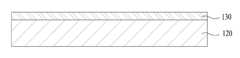
본 실시예에 따른 발광소자 모듈(200)은 한 쌍의 제1,2 도전층(140)이 서로 전기적으로 분리되어 배치되고, 상기 제1,2 도전층(140)과 전기적으로 연결되며 발광소자(100)가 배치되고 있다. 제1, 2 도전층(140)은 절연층(130)을 통하여 방열층(120)과 접촉하고 있다.The light
방열층(120)은 알루미늄(Al) 등 열전도성이 우수한 물질로 이루어질 수 있고, 절연층(130)은 제1,2 도전층(140)으로부터 방출되는 열을 방열층(120)으로 전달하므로 열전도성이 우수한 재료로 이루어질 수 있다.The
방열층(120)의 두께(t1)은 0.6 밀리미터일 수 있고, 절연층(130)의 두께(t2)는 0.1 밀리미터일 수 있는데, 각각의 수치는 10%의 공차를 가질 수 있다.The thickness t1 of the
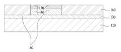
제1,2 도전층(140)의 사이에는 절연층(130) 상에서 PSR층(160)이 배치될 수 있는데, 상기 PSR층(160, Printed Solder Resister)은 발광 소자 모듈의 휘도를 향상시킬 수 있다. 상기 PSR층(160)은 제1,2 도전층(140)의 단락을 막기 위하여 절연성 물질로 이루어질 수 있다.A
제1,2 도전층(140)의 상부에는 전극 패드(150)가 각각 배치될 수 있는데, 전극 패드(150)는 은(Ag)으로 이루어질 수 있다. 도 1에서 전극 패드(150)가 제1, 2 도전층(140)과 동일한 영역에 배치되고 있으나, 전극 패드(150)은 제1,2 도전층(140)의 적어도 일부 영역에 배치될 수 있다.The
제1,2 도전층(140)은 0.05 밀리미터의 두께를 가지고 전극 패드(150)는 0.01 밀리미터의 두께를 가질 수 있는데, 제1,2 도전층(140)의 두께가 전극 패드(150)의 두께의 5배일 수 있으며, 상술한 수치들은 10%의 공차를 가질 수 있다.The first and second
상기 제1, 2 도전층(140)은 상기 발광 소자(100)에서 발생된 광을 반사시켜 광 효율을 증가시킬 수 있는데, 은(Ag)으로 이루어진 전극 패드(150)가 광 반사를 증가시킬 수 있다.The first and second
발광소자(100)는 제1,2 도전층(140)과 전기적으로 연결될 수 있는데, 수직형 발광소자와 수평형 발광소자 또는 플립형 발광소자가 배치될 수 있다. 본 실시예에서 발광소자(100)은 접착층(110)을 통하여 하나의 도전층(140)과 전기적으로 접촉하고, 와이어(105)를 통하여 다른 하나의 도전층과 전기적으로 접촉하고 있다.The
상기 몰딩부(180)는 상기 발광 소자(100)를 둘러싸며 보호할 수 있다. 또한, 상기 몰딩부(180)에는 형광체(185)가 포함되어 상기 발광 소자(100)에서 방출된 광의 파장을 변화시킬 수 있다. 상기 몰딩부(180)는 적어도 발광소자(100)와 와이어(105)를 덮으며 형성될 수 있다.The
그리고, 상기 발광소자(100)에서 방출된 제1 파장 영역의 광이 상기 형광체(185)에 의하여 여기되어 제2 파장 영역의 광으로 변환되고, 상기 제2 파장 영역의 광은 렌즈(미도시) 등의 광 경로 변환 유닛을 통과하면서 광경로가 변경될 수 있다.The light of the first wavelength range emitted from the
렌즈는 발광소자(100)에서 방출되어, 형광체에서 파장이 변환된 빛의 굴절 등을 통하여 광경로를 변환시킬 수 있으며, 특히 백라이트 유닛 내에서 발광소자 모듈이 사용될 때 지향각을 조절할 수 있다.The lens may be emitted from the
렌즈는 광투과율이 좋은 재료로 이루어지는데, 일 예로써 폴리메틸메타크릴레이트(PolyMethylMethAcrylate; PMMA), 폴리카보네이트(PolyCarbonate; PC), 폴리에틸렌(PolyEthylene; PE) 또는 레진 사출물로 이루어질 수 있다.The lens is made of a material having a high light transmittance. For example, the lens may be made of polymethyl methacrylate (PMMA), polycarbonate (PC), polyethylene (PE), or resin injection molding.
그리고, 발광소자(100)의 주변 영역에 댐(170)이 형성될 수 있는데, 댐(170)은 몰딩부(180)의 가장 자리를 고정할 수 있다. 즉, 몰딩부(180)가 발광소자(100)를 둘러싸며 형성된 후, 몰딩부(180)의 가장 자리가 댐(170)에서 고정되어, 몰딩부(180)가 댐(170) 내에 배치되고 있다. 댐(170)은 몰딩부(180)의 둘레를 고정하도록 원형 또는 타원형으로 배치될 수 있다.A
댐(170)의 높이는 40 내지 60 마이크로 미터일 수 있는데, 댐(170)의 높이가 너무 낮으면 몰딩부(180)의 고정에 충분하지 않을 수 있고, 댐(170)의 높이가 너무 높으면 발광소자(100)로부터 수평 방향으로 방출된 빛의 진행에 영향을 미칠 수 있다.If the height of the
그리고, 상기 댐(170)으로부터 기설정된 간격 만큼 이격되어 반사부재(190)가 배치될 수 있다. 본 실시예에서 발광소자(100)의 둘레에 캐비티가 형성되지 않아서 발광소자(100)로부터 방출되는 빛이 발광소자 모듈(200)의 측면으로도 많이 방출될 수 있으므로, 반사 부재(190)가 측면으로 향하는 빛을 반사시켜 발광소자 모듈의 지향각을 조절할 수 있다.The reflecting
반사 부재(190)는 반사율이 뛰어난 물질을 사용할 수 있는데, 도시된 바와 같이 내측벽에 경사면이 형성되어 발광소자(100)로부터 방출된 빛의 반사 효율을 증가시킬 수 있다. 반사 부재(190)를 PSR층(160) 등에 고정할 때, 고정 부재(195)로는 양면 접착제 또는 양면 접착 테이프 등을 사용할 수 있다.As shown in the figure, an inclined surface may be formed on the inner wall of the
반사 부재(190)의 경사면의 최상단의 폭(WR)이 발광소자 모듈로부터 빛이 방출되는 개구부가 되며, 상기 개구부의 폭(WR)은 댐(170)에 고정된 몰딩부(180)의 폭(WV)의 1.5 내지 2 배일 수 있는데, 반사 부재(190)가 타원형을 이루므로 큰 범위를 가지고 있다.The width WR of the top end of the inclined surface of the
본 실시예에서 하나의 발광소자 모듈 내에 하나의 발광소자가 배치되고 있으나, 복수 개의 발광소자가 배치될 수도 있으며 3개의 발광소자가 배치될 때 적색과 녹색 및 청색의 빛을 방출하는 발광소자를 각각 배치할 수도 있다.In the present embodiment, one light emitting element is disposed in one light emitting element module, but a plurality of light emitting elements may be disposed. When three light emitting elements are arranged, the light emitting elements emitting red, green, It can also be deployed.
도 2 내지 도 7은 도 1의 발광소자 모듈의 제조공정을 나타낸 도면이다.2 to 7 are views showing a manufacturing process of the light emitting device module of FIG.
먼저, 도 2에 도시된 바와 같이 방열층(120) 위에 절연층(130)을 준비한다. 방열층(120)은 알루미늄 등으로 이루어질 수 있고, 절연층(130)도 열전도성이 우수한 절연물질로 이루어질 수 있다.First, an insulating
그리고, 도 3에 도시된 바와 같이 절연층(130) 위에 제1,2 도전층(140)과 전극 패드(150)를 형성할 수 있다. 제1,2 도전층(140)은 구리(Cu) 등 전기 전도도가 우수한 물질을 절연층(130)의 표면에 마스크를 씌우고 패터닝하여 형성할 수 있다.The first and second
전극 패드(150)는 제1,2 도전층(140)과 동일한 면적 또는 보다 좁은 면적으로 패터닝하여 형성할 수 있다. 전극 패드(150)는 제1,2 전극층(150)의 반사율을 높일 뿐만 아니라, 제1,2 전극층(150)의 변색을 방지할 수도 있다. 전극 패드(150)는 코팅의 방법으로 형성할 수 있으며, SiO2 또는 TiO2 등으로 복수 개의 층으로 형성할 수도 있다.The
그리고, 도 4에 도시된 바와 같이 제1,2 도전층(140)의 사이를 PSR층(160)로 채워서, 반사 부재나 몰딩부 등이 형성될 영역을 준비하고, 제1,2 도전층(140)의 전기적 단락을 방지할 수 있다.4, the first and second
그리고, 도 5에 도시된 바와 같이 하나의 도전층(140)과 전극 패드(150)에 접착층(110)을 통하여 발광소자(100)를 고정하고, 상기 발광소자(100)를 다른 도전층(140)과 전극 패드(150)에 와이어(105)를 통하여 전기적으로 연결한다.5, the
그리고, 발광소자(100)의 주변 영역에 댐(170)를 형성한다. 상기 댐(170)은 몰딩부를 고정하기 위한 것으로서, PSR층(160) 상에 실크 스크린법 등의 인쇄법으로 형성될 수 있다.A
그리고, 도 6에 도시된 바와 같이 발광소자(100)의 둘레에 몰딩부(180)를 도포하고 경화하여 몰딩부(180)를 형성할 수 있다. 몰딩부(180)는 형광체(185)를 포함할 수 있으며, 몰딩부(180)의 가장 자리는 댐(170)에 고정되어 원형 내지 타원형을 이룰 수 있다.As shown in FIG. 6, the
그리고, 도 7에 도시된 바와 같이 반사 부재(190)를 고정 부재(195)를 통하여, PSR층(160) 위에 고정시킬 수 있다. 상기 PSR층(160)과 반사 부재(190)가 이루는 캐비티가 반사컵으로 작용할 수 있다. 반사 부재(190)는 내측벽이 경사를 이룰 수 있으며, 내습 코팅을 통하여 외부로부터 이물질의 침투를 방지할 수 있다.7, the
도 8 내지 도 11은 발광소자 모듈의 다른 실시예의 단면도이다.8 to 11 are sectional views of another embodiment of the light emitting device module.
도 8에 도시된 실시예에서는 댐(170)의 상부에 'V'자 또는 'U'자 형상의 홈이 형성되고 있으며, 상기 홈에 몰딩부(180)의 가장 자리가 고정되고 있다. 이때, 상기 홈을 통하여 몰딩부(180)의 가장 자리의 고정이 용이할 수 있다.In the embodiment shown in FIG. 8, a 'V' groove or a 'U' groove is formed in the upper part of the
도 9에 도시된 실시예에서는 댐(170)의 상부가 라운드 형상을 하고 있으며, 라운드 형상에 몰딩부(180)의 가장 자리가 고정되고 있다.In the embodiment shown in FIG. 9, the upper part of the
도 10에 도시된 실시예와 도 11에 도시된 실시예에서는 댐(170)의 상부에 단차 내지 홈이 형성되어, 몰딩부(180)의 고정을 용이하게 하고 있다. 도 10에 도시된 실시예에서는 댐(170)의 상부에 단차가 형성되며, 단차는 댐(170)의 가장 자리가 더 높게 배치되고 있다. 그리고, 도 11에 도시된 실시예에서는 댐(170)의 상부에 단차 내지 홈이 형성되어, 몰딩부(180의 가장 자리를 고정시키고 있다.In the embodiment shown in FIG. 10 and the embodiment shown in FIG. 11, a step or a groove is formed on the upper part of the
도 12는 도 1의 'A' 부분의 발광소자의 배선 구조의 일실시예를 나타낸 도면이다.12 is a view showing an embodiment of a wiring structure of a light emitting device in a portion 'A' in FIG.
도 1에서 수평형 발광소자(100)가 배치되고 있으며, 제1 전극(100a)은 제1 도전층(140a)에 와이어(105)로 연결되고 있으며, 제2 전극(100b)은 제2 도전층(140b)에 와이어(105)로 연결되고 있다. 이때, 제1 도전층(140a)과 제2 도전층(140b)의 표면에는 전극 패드가 배치될 수 있다.In FIG. 1, the horizontal
본 실시예에서 수평형 발광소자(100)의 주변에 제1 도전층(140a)과 제2 도전층(140b)이 대각선 방향에 배치되어, 발광소자 모듈 내에서 제1,2 도전층(140a, 140b)의 배치 면적을 줄일 수 있다.The first
도 13은 발광소자 모듈의 또 다른 실시예를 나타낸 도면이다.13 is a view showing another embodiment of the light emitting element module.
본 실시예는 상술한 실시예들과 달리 댐(170)이 생략되고 있으며, 반사 부재(190)가 몰딩부(180)의 가장 자리를 고정시키고 있다. 몰딩부(180)의 높이가 반사 부재(190)의 높이보다 낮게 배치되어 있으나, 더 높게 배치될 수도 있다.In this embodiment, the
도 14는 발광소자 모듈 어레이와 도광판의 배치를 나타낸 도면이다. 도 14에 도시된 실시예와 같이 몰딩부의 높이가 반사 부재의 높이보다 높게 배치되거나, 몰딩부 위에 렌즈가 배치되어 렌즈의 높이가 반사 부재의 높이보다 높게 배치될 때, 발광소자 모듈이 백라이트 유닛에서 사용될 때 아래와 같이 도광판이 배치될 수 있다.14 is a view showing the arrangement of the light emitting element module array and the light guide plate. 14, when the height of the molding part is higher than the height of the reflection member, or when the lens is arranged on the molding part and the height of the lens is higher than the height of the reflection member, When used, the light guide plate can be arranged as follows.
도 14에서 도광판의 한 쪽 모서리에 복수 개의 홈이 형성되어 있으며, 상기 홈에는 발광소자 모듈(200)이 각각 배치되고 있다. 즉, 발광소자 모듈(200)에서 몰딩부나 렌즈의 높이가 가장 높을 때 도광판과 발광소자 모듈(200)이 직접 접촉하면 몰딩부나 렌즈가 손상될 수 있으므로, 도광판에 홈을 형성하여 상술한 몰딩부나 렌즈가 도광판과 직접 접촉하는 것을 방지할 수 있다.14, a plurality of grooves are formed at one edge of the light guide plate, and the light emitting
그리고, 도광판에 형성된 홈의 내측면에 형광체층을 코팅할 수 있는데, 이때 발광소자 모듈의 몰딩부 내의 형광체를 생략할 수 있다.The phosphor layer may be coated on the inner surface of the groove formed in the light guide plate. In this case, the phosphor in the molding portion of the light emitting device module may be omitted.
도 15 내지 도 16은 상술한 발광소자 모듈이 배치된 어레이를 나타낸 도면이다. 15 to 16 are views showing an array in which the above-described light emitting device module is disposed.
제1 도전층(140a)은 발광소자에 구동 신호를 공급할 수 있으므로 각각의 발광소자에 공통될 수 있고 애노드(anode) 전극일 수 있고, 제2 도전층(140b)은 각각의 발광소자 별로 연결될 수 있으며 캐소드(cathode) 전극일 수 있다.The first
도 15에서 발광소자가 배치될 영역의 가장 자리에 댐이 배치될 영역(B)이 도시되어 있고, 제1 도전층(140a) 위에 발광소자가 배치될 영역에 전극 패드(a)가 배치되어 있고, 제2 도전층(140b)이 발광소자와 연결될 영역에 다른 전극 패드(b)가 배치될 수 있다. 이러한 전극 패드의 배치는 수직형 발광소자에 적용될 수 있다. 그리고, 제1,2 도전층(140a, 140b)이 배치되고 다른 영역에는 PSR층(160)이 노출되고 있다.In Fig. 15, a region B in which the dam is to be arranged is shown at the edge of the region where the light emitting element is to be arranged, and the electrode pad a is arranged in the region where the light emitting element is to be placed on the first
도 16에서는 도 15에서 제1 전극층(140a)의 전극 패드(150a) 위에 발광소자(100)가 배치되고, 발광소자(100)가 와이어(105)를 통하여 제2 전극층(140b)와 연결되고 있으며, 댐이 형성된 영역(B)의 가장 자리에 반사 부재(190)가 배치되고 있다.16, the
반사 부재(190)의 형상은 발광소자로부터 방출되는 빛의 투사 영역에 큰 영향을 미치는데, 본 실시예에서는 반사 부재(190)가 타원형으로 배치되고 있는데, 반사 부재(190)의 수평 단면 즉, 제1 도전층과 제2 도전층의 배열과 나란한 방향으로 반사 부재(190)를 절개하였을 때 반사 부재(190)와 상기 반사 부재(190)의 내측면의 경사면의 단면은 타원형을 이루고 있다. 이때, 반사 부재(190)의 내측면의 경사면이 이루는 타원은 장반경이 단반경의 180 내지 220%일 수 있다.The shape of the reflecting
실시 예에 따른 발광소자 모듈은 복수 개가 기판 상에 어레이되고, 상기 발광소자 모듈의 광 경로 상에 광학 부재인 도광판, 프리즘 시트, 확산 시트 등이 배치될 수 있다. 이러한 발광소자 모듈, 기판, 광학 부재는 라이트 유닛으로 기능할 수 있다. 또 다른 실시 예는 상술한 실시 예들에 기재된 반도체 발광소자 또는 발광소자 모듈을 포함하는 표시 장치, 지시 장치, 조명 시스템으로 구현될 수 있으며, 예를 들어, 조명 시스템은 램프, 가로등을 포함할 수 있다.이하에서는 상술한 발광소자 모듈이 배치된 조명 시스템의 일실시예로서, 조명장치와 백라이트 유닛을 설명한다.A light guide plate, a prism sheet, a diffusion sheet, and the like, which are optical members, may be disposed on the light path of the light emitting device module. Such a light emitting element module, substrate, and optical member can function as a light unit. Still another embodiment may be implemented as a display device, an indicating device, and a lighting system including the semiconductor light emitting device or the light emitting device module described in the above embodiments. For example, the lighting system may include a lamp, a streetlight . [0054] Hereinafter, the illumination device and the backlight unit will be described as an embodiment of the illumination system in which the above-described light emitting element module is disposed.
도 17은 발광소자 모듈이 배치된 조명 장치의 일실시예를 나타낸 도면이다.17 is a view showing an embodiment of a lighting apparatus in which a light emitting element module is disposed.
실시예에 따른 조명 장치는 광을 투사하는 광원(600)과 상기 광원(600)이 내장되는 하우징(400)과 상기 광원(600)의 열을 방출하는 방열부(500) 및 상기 광원(600)과 방열부(500)를 상기 하우징(400)에 결합하는 홀더(700)를 포함하여 이루어진다.The illumination device according to the embodiment includes a
상기 하우징(400)은 전기 소켓(미도시)에 결합되는 소켓 결합부(410)와, 상기 소켓결합부(410)와 연결되고 광원(600)이 내장되는 몸체부(420)를 포함한다. 몸체부(420)에는 하나의 공기유동구(430)가 관통하여 형성될 수 있다.The
상기 하우징(400)의 몸체부(420) 상에 복수 개의 공기유동구(430)가 구비되어 있는데, 상기 공기유동구(430)는 하나의 공기유동구로 이루어지거나, 복수 개의 유동구를 도시된 바와 같은 방사상 배치 이외의 다양한 배치도 가능하다.A plurality of
상기 광원(600)은 기판(610) 상에 복수 개의 발광소자 모듈(650)이 구비된다. 여기서, 상기 기판(610)은 상기 하우징(400)의 개구부에 삽입될 수 있는 형상일 수 있으며, 후술하는 바와 같이 방열부(500)로 열을 전달하기 위하여 열전도율이 높은 물질로 이루어질 수 있다.The
상기 광원의 하부에는 홀더(700)가 구비되는데 상기 홀더(700)는 프레임과 또 다른 공기 유동구를 포함할 수 있다. 또한, 도시되지는 않았으나 상기 광원(600)의 하부에는 광학 부재가 구비되어 상기 광원(600)의 발광소자 모듈(650)에서 투사되는 빛을 확산, 산란 또는 수렴시킬 수 있다.A
도 18은 발광소자 모듈을 포함하는 백라이트를 나타낸 도면이다.18 is a view showing a backlight including a light emitting element module.
도시된 바와 같이, 본 실시예에 따른 표시장치(800)는 광원 모듈과, 바텀 커버(820) 상의 반사판(820)과, 상기 반사판(820)의 전방에 배치되며 상기 광원모듈에서 방출되는 빛을 표시장치 전방으로 가이드하는 도광판(840)과, 상기 도광판(840)의 전방에 배치되는 제1 프리즘시트(850)와 제2 프리즘시트(860)와, 상기 제2 프리즘시트(860)의 전방에 배치되는 패널(870)과 상기 패널(870)의 전반에 배치되는 컬러필터(880)를 포함하여 이루어진다.As shown in the figure, the
광원 모듈은 기판(830) 상의 발광소자 모듈(835)을 포함하여 이루어진다. 여기서, 기판(830)은 PCB 등이 사용될 수 있고, 발광소자 모듈(835)은 상술한 바와 같다.The light source module comprises a light emitting
상기 바텀 커버(810)는 표시 장치(800) 내의 구성 요소들을 수납할 수 있다.상기 반사판(820)은 본 도면처럼 별도의 구성요소로 마련될 수도 있고, 상기 도광판(840)의 후면이나, 상기 바텀 커버(810)의 전면에 반사도가 높은 물질로 코팅되는 형태로 마련되는 것도 가능하다.The
여기서, 반사판(820)은 반사율이 높고 초박형으로 사용 가능한 소재를 사용할 수 있고, 폴리에틸렌 테레프탈레이트(PolyEthylene Terephtalate; PET)를 사용할 수 있다.Here, the
도광판(430)은 발광소자 모듈에서 방출되는 빛을 산란시켜 그 빛이 액정 표시 장치의 화면 전영역에 걸쳐 균일하게 분포되도록 한다. 따라서, 도광판(830)은 굴절률과 투과율이 좋은 재료로 이루어지는데, 폴리메틸메타크릴레이트(PolyMethylMethAcrylate; PMMA), 폴리카보네이트(PolyCarbonate; PC), 또는 폴리에틸렌(PolyEthylene; PE) 등으로 형성될 수 있다.The
상기 제1 프리즘 시트(850)는 지지필름의 일면에, 투광성이면서 탄성을 갖는 중합체 재료로 형성되는데, 상기 중합체는 복수 개의 입체구조가 반복적으로 형성된 프리즘층을 가질 수 있다. 여기서, 상기 복수 개의 패턴은 도시된 바와 같이 마루와 골이 반복적으로 스트라이프 타입으로 구비될 수 있다.The
상기 제2 프리즘 시트(860)에서 지지필름 일면의 마루와 골의 방향은, 상기 제1 프리즘 시트(850) 내의 지지필름 일면의 마루와 골의 방향과 수직할 수 있다. 이는 광원 모듈과 반사시트로부터 전달된 빛을 상기 패널(870)의 전방향으로 고르게 분산하기 위함이다.In the
본 실시예에서 상기 제1 프리즘시트(850)과 제2 프리즘시트(860)가 광학시트를 이루는데, 상기 광학시트는 다른 조합 예를 들어, 마이크로 렌즈 어레이로 이루어지거나 확산시트와 마이크로 렌즈 어레이의 조합 또는 하나의 프리즘 시트와 마이크로 렌즈 어레이의 조합 등으로 이루어질 수 있다.In the present embodiment, the
상기 패널(870)은 액정 표시 패널(Liquid crystal display)가 배치될 수 있는데, 액정 표시 패널(860) 외에 광원을 필요로 하는 다른 종류의 디스플레이 장치가 구비될 수 있다.A liquid crystal display (LCD) panel may be disposed on the
상기 패널(870)은, 유리 바디 사이에 액정이 위치하고 빛의 편광성을 이용하기 위해 편광판을 양 유리바디에 올린 상태로 되어있다. 여기서, 액정은 액체와 고체의 중간적인 특성을 가지는데, 액체처럼 유동성을 갖는 유기분자인 액정이 결정처럼 규칙적으로 배열된 상태를 갖는 것으로, 상기 분자 배열이 외부 전계에 의해 변화되는 성질을 이용하여 화상을 표시한다.In the
표시장치에 사용되는 액정 표시 패널은, 액티브 매트릭스(Active Matrix) 방식으로서, 각 화소에 공급되는 전압을 조절하는 스위치로서 트랜지스터를 사용한다.A liquid crystal display panel used in a display device is an active matrix type, and a transistor is used as a switch for controlling a voltage supplied to each pixel.
상기 패널(870)의 전면에는 컬러 필터(880)가 구비되어 상기 패널(870)에서 투사된 빛을, 각각의 화소마다 적색과 녹색 및 청색의 빛만을 투과하므로 화상을 표현할 수 있다.A
도 19는 도 18의 표시 장치에서 발광소자 모듈의 구동의 일실시예를 나타낸 도면이다.19 is a diagram showing an embodiment of driving the light emitting device module in the display device of FIG.
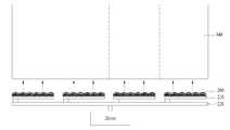
발광소자 모듈의 구동 유닛(Driver)은 기판(220)과 커텍터(Connector)를 통하여 각각의 스트링(210)으로 구동 신호 내지 전류를 공급하는데, 각각의 스트링(210)에는 6개 내지 8개의 발광소자 모듈(200)이 배치되어 있다. 이때, 각각의 스트링(210)에 배치된 발광소자 모듈(200)마다 구동 신호를 달리 공급하면 도광판(840)에서 점선으로 구분된 영역마다 분할하여 빛을 공급할 수 있다.The driving unit driver of the light emitting device module supplies driving signals or currents to the
이상에서 실시예를 중심으로 설명하였으나 이는 단지 예시일 뿐 본 발명을 한정하는 것이 아니며, 본 발명이 속하는 분야의 통상의 지식을 가진 자라면 본 실시예의 본질적인 특성을 벗어나지 않는 범위에서 이상에 예시되지 않은 여러 가지의 변형과 응용이 가능함을 알 수 있을 것이다. 예를 들어, 실시예에 구체적으로 나타난 각 구성 요소는 변형하여 실시할 수 있는 것이다. 그리고 이러한 변형과 응용에 관계된 차이점들은 첨부된 청구 범위에서 규정하는 본 발명의 범위에 포함되는 것으로 해석되어야 할 것이다.While the present invention has been particularly shown and described with reference to exemplary embodiments thereof, it is to be understood that the invention is not limited to the disclosed exemplary embodiments, but, on the contrary, It will be understood that various modifications and applications are possible. For example, each component specifically shown in the embodiments can be modified and implemented. It is to be understood that all changes and modifications that come within the meaning and range of equivalency of the claims are therefore intended to be embraced therein.
100 : 발광소자 105 : 와이어
110 : 접착층 120 : 방열층
130 : 절연층 140 : 제1,2 도전층
150 : 전극 패드 160 : PSR층
170 : 댐 180 : 몰딩부
185 : 형광체 190 : 반사 부재
195 : 고정 부재 200 : 발광소자 모듈
210 : 스트링 220 : 기판
400 : 하우징 500 : 방열부
600 : 광원 700 : 홀더
800 : 표시장치 810 : 바텀 커버
820 : 반사판 830 : 회로 기판 모듈
840 : 도광판 850, 860 : 제1,2 프리즘 시트
870 : 패널 880 : 컬러필터100: light emitting element 105: wire
110: adhesive layer 120: heat radiation layer
130: insulating layer 140: first and second conductive layers
150: electrode pad 160: PSR layer
170: dam 180: molding part
185: phosphor 190: reflective member
195: fixing member 200: light emitting element module
210: string 220: substrate
400: housing 500:
600: light source 700: holder
800: Display device 810: Bottom cover
820: reflector 830: circuit board module
840:
870: Panel 880: Color filter
Claims (18)
Translated fromKorean상기 발광소자 모듈로부터 방출되는 빛을 전달하는 도광판을 포함하고,
상기 복수의 발광소자 모듈 각각은,
서로 전기적으로 분리되는 제1 도전층과 제2 도전층;
상기 제1 도전층과 제2 도전층의 적어도 일부 영역 위에 배치되는 전극 패드;
상기 제1 도전층과 제2 도전층의 사이에 배치되는 PSR층;
상기 제1 도전층 및 제2 도전층과 전기적으로 연결되는 발광소자;
상기 발광소자의 주변 영역에 배치되는 댐;
상기 발광소자를 둘러싸고, 상기 댐 내에 배치되는 몰딩부; 및
상기 댐의 주변 영역에 배치되고, 내측벽 경사면으로 형성된 반사부재를 포함하고,
상기 도광판은,
상기 복수 개의 발광소자 모듈 각각과 대응하여 형성된 복수 개의 홈; 및
상기 홈의 내측면에 배치되어, 상기 몰딩부와 상기 도광판을 이격시키는 형광체층을 포함하는 조명 시스템.A plurality of light emitting device modules; And
And a light guide plate for transmitting light emitted from the light emitting device module,
Wherein each of the plurality of light emitting device modules includes:
A first conductive layer and a second conductive layer electrically separated from each other;
An electrode pad disposed on at least a portion of the first conductive layer and the second conductive layer;
A PSR layer disposed between the first conductive layer and the second conductive layer;
A light emitting element electrically connected to the first conductive layer and the second conductive layer;
A dam disposed in a peripheral region of the light emitting element;
A molding part surrounding the light emitting device and disposed in the dam; And
And a reflecting member disposed in a peripheral region of the dam and formed of an inner wall inclined surface,
The light-
A plurality of grooves formed corresponding to each of the plurality of light emitting device modules; And
And a phosphor layer disposed on an inner surface of the groove to separate the molding portion from the light guide plate.
상기 전극 패드는 은(Ag)으로 이루어지고,
상기 댐은 상기 PSR층 상에 인쇄되어 형성된 조명 시스템.The method according to claim 1,
Wherein the electrode pad is made of silver (Ag)
Wherein the dam is printed on the PSR layer.
상기 댐은 상기 발광소자 둘레에 원형으로 배치되고,
상기 경사면의 수평 단면은 상기 발광소자의 둘레에서 타원을 이루는 조명 시스템.The method according to claim 1,
Wherein the dam is circularly arranged around the light emitting element,
Wherein the horizontal cross section of the slope forms an ellipse around the light emitting element.
상기 댐은 상부에 적어도 하나의 단차를 가지고, 상기 단차에 상기 몰딩부의 가장 자리가 고정되는 조명 시스템.The method according to claim 1 or 4,
Wherein the dam has at least one step in its upper part, the edge of the molding part being fixed to the step.
상기 댐은 상부에 홈이 형성되고, 상기 홈에 상기 몰딩부의 가장 자리가 고정되는 조명 시스템.The method according to claim 1 or 4,
Wherein the dam is formed with a groove on an upper portion thereof and the edge of the molding portion is fixed to the groove.
상기 제1 도전층과 제2 도전층은, 절연층을 사이에 두고 방열층과 접촉하는 조명 시스템.The method according to claim 1 or 4,
Wherein the first conductive layer and the second conductive layer are in contact with the heat dissipation layer with an insulating layer therebetween.
상기 반사 부재는 상기 PSR층 상에 배치되고,
상기 반사 부재와 상기 PSR층은 고정부재로 결합되고,
상기 고정 부재는 양면 접착제 또는 양면 접착 테이프인 조명 시스템.The method according to claim 1 or 4,
Wherein the reflective member is disposed on the PSR layer,
Wherein the reflective member and the PSR layer are coupled by a fixing member,
Wherein the fixing member is a double-sided adhesive or a double-sided adhesive tape.
상기 반사 부재의 경사면의 최상단의 폭은 상기 댐에 고정된 몰딩부의 폭의 1.5 내지 2 배로 형성된 조명 시스템.
The method according to claim 1 or 4,
Wherein the width of the uppermost end of the inclined surface of the reflecting member is 1.5 to 2 times the width of the molding part fixed to the dam.
Priority Applications (8)
| Application Number | Priority Date | Filing Date | Title |
|---|---|---|---|
| KR1020110064717AKR101813166B1 (en) | 2011-06-30 | 2011-06-30 | Light emitting device module and lighting system including the same |
| US13/412,820US8878215B2 (en) | 2011-06-22 | 2012-03-06 | Light emitting device module |
| JP2012051938AJP2013008941A (en) | 2011-06-22 | 2012-03-08 | Light emitting device module |
| TW101108092ATWI546984B (en) | 2011-06-22 | 2012-03-09 | Light-emitting element module |
| EP12160221.3AEP2538462B1 (en) | 2011-06-22 | 2012-03-19 | Light emitting device module |
| CN201210100153.4ACN102842670B (en) | 2011-06-22 | 2012-04-06 | Light emitting device module |
| US14/505,362US9705054B2 (en) | 2011-06-22 | 2014-10-02 | Light emitting device module |
| JP2016224526AJP6339161B2 (en) | 2011-06-22 | 2016-11-17 | Light emitting device package |
Applications Claiming Priority (1)
| Application Number | Priority Date | Filing Date | Title |
|---|---|---|---|
| KR1020110064717AKR101813166B1 (en) | 2011-06-30 | 2011-06-30 | Light emitting device module and lighting system including the same |
Publications (2)
| Publication Number | Publication Date |
|---|---|
| KR20130007242A KR20130007242A (en) | 2013-01-18 |
| KR101813166B1true KR101813166B1 (en) | 2018-01-30 |
Family
ID=47837851
Family Applications (1)
| Application Number | Title | Priority Date | Filing Date |
|---|---|---|---|
| KR1020110064717AExpired - Fee RelatedKR101813166B1 (en) | 2011-06-22 | 2011-06-30 | Light emitting device module and lighting system including the same |
Country Status (1)
| Country | Link |
|---|---|
| KR (1) | KR101813166B1 (en) |
Families Citing this family (1)
| Publication number | Priority date | Publication date | Assignee | Title |
|---|---|---|---|---|
| KR102385941B1 (en)* | 2015-06-15 | 2022-04-13 | 쑤저우 레킨 세미컨덕터 컴퍼니 리미티드 | Light Emitting Device Package |
Citations (3)
| Publication number | Priority date | Publication date | Assignee | Title |
|---|---|---|---|---|
| JP2006108606A (en)* | 2004-10-05 | 2006-04-20 | Samsung Electronics Co Ltd | White light generation unit, backlight assembly having the same, and liquid crystal display device having the same |
| JP2008227166A (en)* | 2007-03-13 | 2008-09-25 | Sharp Corp | Semiconductor light emitting device, multiple lead frame for semiconductor light emitting device |
| JP2010003994A (en)* | 2008-06-23 | 2010-01-07 | Sharp Corp | Lighting device, backlight device, and method of manufacturing lighting device |
- 2011
- 2011-06-30KRKR1020110064717Apatent/KR101813166B1/ennot_activeExpired - Fee Related
Patent Citations (3)
| Publication number | Priority date | Publication date | Assignee | Title |
|---|---|---|---|---|
| JP2006108606A (en)* | 2004-10-05 | 2006-04-20 | Samsung Electronics Co Ltd | White light generation unit, backlight assembly having the same, and liquid crystal display device having the same |
| JP2008227166A (en)* | 2007-03-13 | 2008-09-25 | Sharp Corp | Semiconductor light emitting device, multiple lead frame for semiconductor light emitting device |
| JP2010003994A (en)* | 2008-06-23 | 2010-01-07 | Sharp Corp | Lighting device, backlight device, and method of manufacturing lighting device |
Also Published As
| Publication number | Publication date |
|---|---|
| KR20130007242A (en) | 2013-01-18 |
Similar Documents
| Publication | Publication Date | Title |
|---|---|---|
| JP6339161B2 (en) | Light emitting device package | |
| US8899811B2 (en) | Light emitting device module and backlight unit including the same | |
| KR101850434B1 (en) | Light emitting device module and lighting system including the same | |
| US8816512B2 (en) | Light emitting device module | |
| KR101824434B1 (en) | Light emitting device package, lighting system and image display device including the same | |
| KR20130006823A (en) | Light emitting device package and lighting system including the same | |
| KR101813166B1 (en) | Light emitting device module and lighting system including the same | |
| KR101813167B1 (en) | Light emitting device module and lighting system including the same | |
| KR101894349B1 (en) | Light emitting device package and lighting system including the same | |
| KR101830721B1 (en) | Light emitting device module | |
| KR101820694B1 (en) | Light emitting device package and lighting system including the same | |
| KR101928358B1 (en) | Light emitting device package | |
| KR101797596B1 (en) | Light emitting device package and lighting apparatus including the same | |
| KR101861634B1 (en) | Light emitting device package | |
| KR101874903B1 (en) | Light emitting device module and lighting system including the same | |
| KR101863868B1 (en) | Light emitting device module and illumination system including the same | |
| KR20120130927A (en) | Light emitting device package and light system including the same | |
| KR101804406B1 (en) | Light emitting device package and lighting system including the same | |
| KR101797600B1 (en) | Light emitting device module | |
| KR20150140027A (en) | Light emitting device package | |
| CN102842670B (en) | Light emitting device module | |
| KR102220504B1 (en) | Light Emitting Module | |
| KR101838018B1 (en) | light emitting device package and lighting system including the same | |
| KR20130013508A (en) | Light emitting device module and lighting system including the same | |
| KR20120006171A (en) | Driving method of backlight unit and light emitting device package array |
Legal Events
| Date | Code | Title | Description |
|---|---|---|---|
| PA0109 | Patent application | St.27 status event code:A-0-1-A10-A12-nap-PA0109 | |
| PG1501 | Laying open of application | St.27 status event code:A-1-1-Q10-Q12-nap-PG1501 | |
| PN2301 | Change of applicant | St.27 status event code:A-3-3-R10-R13-asn-PN2301 St.27 status event code:A-3-3-R10-R11-asn-PN2301 | |
| R17-X000 | Change to representative recorded | St.27 status event code:A-3-3-R10-R17-oth-X000 | |
| A201 | Request for examination | ||
| E13-X000 | Pre-grant limitation requested | St.27 status event code:A-2-3-E10-E13-lim-X000 | |
| P11-X000 | Amendment of application requested | St.27 status event code:A-2-2-P10-P11-nap-X000 | |
| P13-X000 | Application amended | St.27 status event code:A-2-2-P10-P13-nap-X000 | |
| PA0201 | Request for examination | St.27 status event code:A-1-2-D10-D11-exm-PA0201 | |
| R18-X000 | Changes to party contact information recorded | St.27 status event code:A-3-3-R10-R18-oth-X000 | |
| E902 | Notification of reason for refusal | ||
| PE0902 | Notice of grounds for rejection | St.27 status event code:A-1-2-D10-D21-exm-PE0902 | |
| E13-X000 | Pre-grant limitation requested | St.27 status event code:A-2-3-E10-E13-lim-X000 | |
| P11-X000 | Amendment of application requested | St.27 status event code:A-2-2-P10-P11-nap-X000 | |
| P13-X000 | Application amended | St.27 status event code:A-2-2-P10-P13-nap-X000 | |
| E701 | Decision to grant or registration of patent right | ||
| PE0701 | Decision of registration | St.27 status event code:A-1-2-D10-D22-exm-PE0701 | |
| GRNT | Written decision to grant | ||
| PR0701 | Registration of establishment | St.27 status event code:A-2-4-F10-F11-exm-PR0701 | |
| PR1002 | Payment of registration fee | St.27 status event code:A-2-2-U10-U11-oth-PR1002 Fee payment year number:1 | |
| PG1601 | Publication of registration | St.27 status event code:A-4-4-Q10-Q13-nap-PG1601 | |
| R18-X000 | Changes to party contact information recorded | St.27 status event code:A-5-5-R10-R18-oth-X000 | |
| R18-X000 | Changes to party contact information recorded | St.27 status event code:A-5-5-R10-R18-oth-X000 | |
| PR1001 | Payment of annual fee | St.27 status event code:A-4-4-U10-U11-oth-PR1001 Fee payment year number:4 | |
| PN2301 | Change of applicant | St.27 status event code:A-5-5-R10-R13-asn-PN2301 St.27 status event code:A-5-5-R10-R11-asn-PN2301 | |
| PN2301 | Change of applicant | St.27 status event code:A-5-5-R10-R11-asn-PN2301 | |
| PN2301 | Change of applicant | St.27 status event code:A-5-5-R10-R14-asn-PN2301 | |
| PR1001 | Payment of annual fee | St.27 status event code:A-4-4-U10-U11-oth-PR1001 Fee payment year number:5 | |
| PR1001 | Payment of annual fee | St.27 status event code:A-4-4-U10-U11-oth-PR1001 Fee payment year number:6 | |
| PR1001 | Payment of annual fee | St.27 status event code:A-4-4-U10-U11-oth-PR1001 Fee payment year number:7 | |
| PC1903 | Unpaid annual fee | St.27 status event code:A-4-4-U10-U13-oth-PC1903 Not in force date:20241222 Payment event data comment text:Termination Category : DEFAULT_OF_REGISTRATION_FEE | |
| P22-X000 | Classification modified | St.27 status event code:A-4-4-P10-P22-nap-X000 | |
| PC1903 | Unpaid annual fee | St.27 status event code:N-4-6-H10-H13-oth-PC1903 Ip right cessation event data comment text:Termination Category : DEFAULT_OF_REGISTRATION_FEE Not in force date:20241222 |