KR101812761B1 - Light emitting diode package - Google Patents
Light emitting diode packageDownload PDFInfo
- Publication number
- KR101812761B1 KR101812761B1KR1020110018519AKR20110018519AKR101812761B1KR 101812761 B1KR101812761 B1KR 101812761B1KR 1020110018519 AKR1020110018519 AKR 1020110018519AKR 20110018519 AKR20110018519 AKR 20110018519AKR 101812761 B1KR101812761 B1KR 101812761B1
- Authority
- KR
- South Korea
- Prior art keywords
- lead frame
- light emitting
- emitting diode
- hole cup
- region
- Prior art date
- Legal status (The legal status is an assumption and is not a legal conclusion. Google has not performed a legal analysis and makes no representation as to the accuracy of the status listed.)
- Active
Links
Images


Classifications
- H—ELECTRICITY
- H10—SEMICONDUCTOR DEVICES; ELECTRIC SOLID-STATE DEVICES NOT OTHERWISE PROVIDED FOR
- H10H—INORGANIC LIGHT-EMITTING SEMICONDUCTOR DEVICES HAVING POTENTIAL BARRIERS
- H10H20/00—Individual inorganic light-emitting semiconductor devices having potential barriers, e.g. light-emitting diodes [LED]
- H10H20/80—Constructional details
- H10H20/85—Packages
- H10H20/857—Interconnections, e.g. lead-frames, bond wires or solder balls
- H—ELECTRICITY
- H10—SEMICONDUCTOR DEVICES; ELECTRIC SOLID-STATE DEVICES NOT OTHERWISE PROVIDED FOR
- H10H—INORGANIC LIGHT-EMITTING SEMICONDUCTOR DEVICES HAVING POTENTIAL BARRIERS
- H10H29/00—Integrated devices, or assemblies of multiple devices, comprising at least one light-emitting semiconductor element covered by group H10H20/00
- H10H29/80—Constructional details
- H10H29/85—Packages
- H10H29/857—Interconnections
- H—ELECTRICITY
- H01—ELECTRIC ELEMENTS
- H01L—SEMICONDUCTOR DEVICES NOT COVERED BY CLASS H10
- H01L25/00—Assemblies consisting of a plurality of semiconductor or other solid state devices
- H01L25/03—Assemblies consisting of a plurality of semiconductor or other solid state devices all the devices being of a type provided for in a single subclass of subclasses H10B, H10D, H10F, H10H, H10K or H10N, e.g. assemblies of rectifier diodes
- H01L25/04—Assemblies consisting of a plurality of semiconductor or other solid state devices all the devices being of a type provided for in a single subclass of subclasses H10B, H10D, H10F, H10H, H10K or H10N, e.g. assemblies of rectifier diodes the devices not having separate containers
- H01L25/075—Assemblies consisting of a plurality of semiconductor or other solid state devices all the devices being of a type provided for in a single subclass of subclasses H10B, H10D, H10F, H10H, H10K or H10N, e.g. assemblies of rectifier diodes the devices not having separate containers the devices being of a type provided for in group H10H20/00
- H01L25/0753—Assemblies consisting of a plurality of semiconductor or other solid state devices all the devices being of a type provided for in a single subclass of subclasses H10B, H10D, H10F, H10H, H10K or H10N, e.g. assemblies of rectifier diodes the devices not having separate containers the devices being of a type provided for in group H10H20/00 the devices being arranged next to each other
- H—ELECTRICITY
- H10—SEMICONDUCTOR DEVICES; ELECTRIC SOLID-STATE DEVICES NOT OTHERWISE PROVIDED FOR
- H10H—INORGANIC LIGHT-EMITTING SEMICONDUCTOR DEVICES HAVING POTENTIAL BARRIERS
- H10H29/00—Integrated devices, or assemblies of multiple devices, comprising at least one light-emitting semiconductor element covered by group H10H20/00
- H10H29/20—Assemblies of multiple devices comprising at least one light-emitting semiconductor device covered by group H10H20/00
- H10H29/24—Assemblies of multiple devices comprising at least one light-emitting semiconductor device covered by group H10H20/00 comprising multiple light-emitting semiconductor devices
- H—ELECTRICITY
- H10—SEMICONDUCTOR DEVICES; ELECTRIC SOLID-STATE DEVICES NOT OTHERWISE PROVIDED FOR
- H10H—INORGANIC LIGHT-EMITTING SEMICONDUCTOR DEVICES HAVING POTENTIAL BARRIERS
- H10H29/00—Integrated devices, or assemblies of multiple devices, comprising at least one light-emitting semiconductor element covered by group H10H20/00
- H10H29/80—Constructional details
- H10H29/85—Packages
- H10H29/8506—Containers
- H—ELECTRICITY
- H01—ELECTRIC ELEMENTS
- H01L—SEMICONDUCTOR DEVICES NOT COVERED BY CLASS H10
- H01L2224/00—Indexing scheme for arrangements for connecting or disconnecting semiconductor or solid-state bodies and methods related thereto as covered by H01L24/00
- H01L2224/01—Means for bonding being attached to, or being formed on, the surface to be connected, e.g. chip-to-package, die-attach, "first-level" interconnects; Manufacturing methods related thereto
- H01L2224/42—Wire connectors; Manufacturing methods related thereto
- H01L2224/47—Structure, shape, material or disposition of the wire connectors after the connecting process
- H01L2224/48—Structure, shape, material or disposition of the wire connectors after the connecting process of an individual wire connector
- H01L2224/4805—Shape
- H01L2224/4809—Loop shape
- H01L2224/48091—Arched
- H—ELECTRICITY
- H01—ELECTRIC ELEMENTS
- H01L—SEMICONDUCTOR DEVICES NOT COVERED BY CLASS H10
- H01L2224/00—Indexing scheme for arrangements for connecting or disconnecting semiconductor or solid-state bodies and methods related thereto as covered by H01L24/00
- H01L2224/01—Means for bonding being attached to, or being formed on, the surface to be connected, e.g. chip-to-package, die-attach, "first-level" interconnects; Manufacturing methods related thereto
- H01L2224/42—Wire connectors; Manufacturing methods related thereto
- H01L2224/47—Structure, shape, material or disposition of the wire connectors after the connecting process
- H01L2224/48—Structure, shape, material or disposition of the wire connectors after the connecting process of an individual wire connector
- H01L2224/481—Disposition
- H01L2224/48151—Connecting between a semiconductor or solid-state body and an item not being a semiconductor or solid-state body, e.g. chip-to-substrate, chip-to-passive
- H01L2224/48221—Connecting between a semiconductor or solid-state body and an item not being a semiconductor or solid-state body, e.g. chip-to-substrate, chip-to-passive the body and the item being stacked
- H01L2224/48245—Connecting between a semiconductor or solid-state body and an item not being a semiconductor or solid-state body, e.g. chip-to-substrate, chip-to-passive the body and the item being stacked the item being metallic
- H01L2224/48247—Connecting between a semiconductor or solid-state body and an item not being a semiconductor or solid-state body, e.g. chip-to-substrate, chip-to-passive the body and the item being stacked the item being metallic connecting the wire to a bond pad of the item
- H—ELECTRICITY
- H01—ELECTRIC ELEMENTS
- H01L—SEMICONDUCTOR DEVICES NOT COVERED BY CLASS H10
- H01L2224/00—Indexing scheme for arrangements for connecting or disconnecting semiconductor or solid-state bodies and methods related thereto as covered by H01L24/00
- H01L2224/01—Means for bonding being attached to, or being formed on, the surface to be connected, e.g. chip-to-package, die-attach, "first-level" interconnects; Manufacturing methods related thereto
- H01L2224/42—Wire connectors; Manufacturing methods related thereto
- H01L2224/47—Structure, shape, material or disposition of the wire connectors after the connecting process
- H01L2224/48—Structure, shape, material or disposition of the wire connectors after the connecting process of an individual wire connector
- H01L2224/481—Disposition
- H01L2224/48151—Connecting between a semiconductor or solid-state body and an item not being a semiconductor or solid-state body, e.g. chip-to-substrate, chip-to-passive
- H01L2224/48221—Connecting between a semiconductor or solid-state body and an item not being a semiconductor or solid-state body, e.g. chip-to-substrate, chip-to-passive the body and the item being stacked
- H01L2224/48245—Connecting between a semiconductor or solid-state body and an item not being a semiconductor or solid-state body, e.g. chip-to-substrate, chip-to-passive the body and the item being stacked the item being metallic
- H01L2224/48257—Connecting between a semiconductor or solid-state body and an item not being a semiconductor or solid-state body, e.g. chip-to-substrate, chip-to-passive the body and the item being stacked the item being metallic connecting the wire to a die pad of the item
- H—ELECTRICITY
- H01—ELECTRIC ELEMENTS
- H01L—SEMICONDUCTOR DEVICES NOT COVERED BY CLASS H10
- H01L2224/00—Indexing scheme for arrangements for connecting or disconnecting semiconductor or solid-state bodies and methods related thereto as covered by H01L24/00
- H01L2224/01—Means for bonding being attached to, or being formed on, the surface to be connected, e.g. chip-to-package, die-attach, "first-level" interconnects; Manufacturing methods related thereto
- H01L2224/42—Wire connectors; Manufacturing methods related thereto
- H01L2224/47—Structure, shape, material or disposition of the wire connectors after the connecting process
- H01L2224/49—Structure, shape, material or disposition of the wire connectors after the connecting process of a plurality of wire connectors
- H01L2224/491—Disposition
- H01L2224/49105—Connecting at different heights
- H01L2224/49109—Connecting at different heights outside the semiconductor or solid-state body
- H—ELECTRICITY
- H01—ELECTRIC ELEMENTS
- H01L—SEMICONDUCTOR DEVICES NOT COVERED BY CLASS H10
- H01L25/00—Assemblies consisting of a plurality of semiconductor or other solid state devices
- H01L25/16—Assemblies consisting of a plurality of semiconductor or other solid state devices the devices being of types provided for in two or more different subclasses of H10B, H10D, H10F, H10H, H10K or H10N, e.g. forming hybrid circuits
- H01L25/167—Assemblies consisting of a plurality of semiconductor or other solid state devices the devices being of types provided for in two or more different subclasses of H10B, H10D, H10F, H10H, H10K or H10N, e.g. forming hybrid circuits comprising optoelectronic devices, e.g. LED, photodiodes
- H—ELECTRICITY
- H10—SEMICONDUCTOR DEVICES; ELECTRIC SOLID-STATE DEVICES NOT OTHERWISE PROVIDED FOR
- H10H—INORGANIC LIGHT-EMITTING SEMICONDUCTOR DEVICES HAVING POTENTIAL BARRIERS
- H10H20/00—Individual inorganic light-emitting semiconductor devices having potential barriers, e.g. light-emitting diodes [LED]
- H10H20/80—Constructional details
- H10H20/85—Packages
- H10H20/8506—Containers
Landscapes
- Engineering & Computer Science (AREA)
- Power Engineering (AREA)
- Microelectronics & Electronic Packaging (AREA)
- Physics & Mathematics (AREA)
- Condensed Matter Physics & Semiconductors (AREA)
- General Physics & Mathematics (AREA)
- Computer Hardware Design (AREA)
- Led Device Packages (AREA)
Abstract
Translated fromKoreanDescription
Translated fromKorean본 발명은 발광다이오드 패키지에 관한 것이며, 더 상세하게는, 신뢰성이 좋은 발광다이오드 패키지에 관한 것이다.The present invention relates to a light emitting diode package, and more particularly, to a light emitting diode package having a high reliability.
일반적으로, 발광다이오드 패키지는 발광다이오드 칩과 발광다이오드 칩에 전력을 인가하기 위한 리드프레임들을 포함한다. 리드프레임들은 패키지 몸체에 의해 지지되며, 발광다이오드 칩은 본딩와이어에 의해 리드프레임들과 전기적으로 연결된다. 패키지 몸체는 리드프레임들을 지지하는 역할 외에 발광다이오드 칩을 내부에 수용하여 보호하는 역할도 한다.Generally, the light emitting diode package includes a light emitting diode chip and lead frames for applying power to the light emitting diode chip. The lead frames are supported by the package body, and the light emitting diode chip is electrically connected to the lead frames by a bonding wire. The package body also serves to support the lead frames and to receive and protect the LED chips.
종래에는 한 쌍의 발광다이오드 칩을 서로 대향된 한 쌍의 리드프레임 각각에 실장한 구조의 발광다이오드 패키지가 개발되었다.A light emitting diode package having a structure in which a pair of light emitting diode chips are mounted on each of a pair of lead frames facing each other has been developed.
도 1은 종래의 발광다이오드 패키지를 도시한 평면도이다.1 is a plan view showing a conventional light emitting diode package.
도 1을 참조하면, 한 쌍의 리드프레임(2a, 2b)이 일자형의 갭에 의해 서로 이격되도록 배치되며, 이 한 쌍의 리드프레임(2a, 2b)은 플라스틱 소재의 패키지 몸체(4)에 의해 지지된다. 한 쌍의 리드프레임(2a, 2b) 각각의 대응되게 한 쌍의 발광다이오드 칩(6a, 6b)이 실장된다. 패키지 몸체(4)는 한 쌍의 발광다이오드 칩(6a, 6b)을 노출시키는 캐비티를 포함하며, 캐비티 내에는 발광다이오드 칩(6a, 6b)으로부터 광을 투과할 수 있는 투광성의 봉지재가 충전된다.Referring to Fig. 1, a pair of
종래의 발광다이오드 패키지에 있어서, 하나의 본딩와이어(w1)가 제1 리드프레임(2a) 상에 있는 제1 발광다이오드 칩(6a)과 이웃하는 제2 리드프레임(2b) 사이를 연결하고, 다른 본딩와이어(w2)가 제2 리드프레임(2b) 상에 있는 제2 발광다이오드 칩(6b)과 제1 리드프레임(2a) 사이를 연결한다.In the conventional light emitting diode package, one bonding wire w1 connects between the first light
발광다이오드 칩(6a 또는 6b)과 리드프레임(2a 또는 2b)의 내측 단부 사이에는 충분한 와이어 본딩 영역이 확보되어야 하며, 이는 제1 발광다이오드 칩(6a)과 제2 발광다이오드 칩(6b) 사이의 거리를 좁히는 설계에 있어서 많은 제한을 야기한다. 또한, 발광다이오드 칩(6a 또는 6b)과 리드프레임(2a 또는 2b)의 내측 단부 사이에 충분한 영역이 확보되지 않은 경우, 제너다이오드(7)의 설치 위치를 정하는데 있어서도 많은 제한을 야기한다.A sufficient wire bonding area must be ensured between the light
발광다이오드 칩을 수용하는 홀컵을 리드프레임에 형성하는 기술을 발광다이오드 패키지에 적용하면, 발광다이오드 패키지의 광 효율과 방열 성능을 향상시킬 수 있다. 그러나, 이 기술을 전술한 종래의 발광다이오드 패키지에 적용하는 것은 쉽지 않은데, 이는 충분치 않은 리드프레임의 와이어 본딩 영역으로 인해 홀컵의 크기가 제한되기 때문이다.When a technique of forming a hole cup for accommodating a light emitting diode chip in a lead frame is applied to the light emitting diode package, the light efficiency and heat dissipation performance of the light emitting diode package can be improved. However, it is not easy to apply this technique to the above-described conventional light emitting diode package because the size of the hole cup is limited due to the wire bonding area of the insufficient lead frame.
본 발명이 해결하려는 하나의 과제는, 이웃하는 리드프레임들에 설치된 발광다이오드 칩 사이의 거리를 늘리지 않고도, 리드프레임들의 와이어 본딩 영역 또는 제너다이오드 설치 영역을 증가시킬 수 있는 발광다이오드 패키지를 제공하는 것이다.One object to be solved by the present invention is to provide a light emitting diode package capable of increasing a wire bonding region of lead frames or a zener diode mounting region without increasing the distance between light emitting diode chips mounted on neighboring lead frames .
본 발명이 해결하려는 다른 과제는, 이웃하는 리드프레임들 각각에 홀컵을 적용하되, 홀컵의 크기 감소 없이도, 리드프레임들의 와이어 본딩 영역 및/또는 제너다이오드 설치 영역을 증가시킬 수 있는 발광다이오드 패키지를 제공하는 것이다.Another object of the present invention is to provide a light emitting diode package capable of increasing the wire bonding area and / or the zener diode mounting area of the lead frames, without applying a size reduction to the hole cup, by applying a hole cup to each of the neighboring lead frames .
본 발명의 일 측면에 따른 발광다이오드 패키지는, 제1 홀컵이 형성된 제1 리드프레임과; 제2 홀컵이 형성되되, 상기 제1 리드프레임과 갭을 두고 대향되게 배치된 제2 리드프레임과; 상기 제1 홀컵 내에 배치되는 제1 발광다이오드 칩과; 상기 제2 홀컵 내에 배치되는 제2 발광다이오드 칩을 포함하며, 상기 제1 리드프레임과 상기 제2 리드프레임 각각은 상기 갭과 상기 제1 홀컵과의 사이 그리고 상기 갭과 상기 제2 홀컵 사이에 인접 영역보다 넓은 제1 확장 영역 및 제2 확장 영역을 각각 포함한다.A light emitting diode package according to an aspect of the present invention includes: a first lead frame having a first hole cup; A second lead frame having a second hole cup formed therein, the second lead frame being opposed to the first lead frame with a gap therebetween; A first light emitting diode chip disposed in the first hole cup; And a second light emitting diode chip disposed in the second hole cup, wherein each of the first lead frame and the second lead frame is disposed between the gap and the first hole cup, and between the gap and the second hole cup Area and a second extended area wider than the first extended area and the second extended area, respectively.
일 실시예에 따라, 상기 제1 확장 영역과 상기 제2 확장 영역은 상기 갭의 굴곡진 모양 또는 사선 모양에 의해 형성될 수 있다.According to an embodiment, the first extension region and the second extension region may be formed by a curved shape or an oblique shape of the gap.
일 실시예에 따라, 상기 제1 발광다이오드 칩으로부터 이어진 본딩와이어의 일단부가 상기 제2 확장 영역에 본딩되고 상기 제2 발광다이오드 칩으로부터 이어진 본딩와이어의 일단부가 상기 제1 확장 영역에 본딩될 수 있다.According to an embodiment, one end of the bonding wire extending from the first LED chip is bonded to the second extension region, and one end of the bonding wire extended from the second LED chip may be bonded to the first extension region .
일 실시예에 따라, 상기 제1 확장 영역 또는 상기 제2 확장 영역에는 제너다이오드가 설치될 수 있다.According to one embodiment, a zener diode may be provided in the first extension region or the second extension region.
일 실시예에 따라, 상기 제1 확장 영역과 상기 제2 확장 영역은 상기 갭을 사이에 두고 대각선 방향으로 마주할 수 있다.According to an embodiment, the first extension region and the second extension region may face diagonally with the gap therebetween.
본 발명의 다른 측면에 따른 발광다이오드 패키지는, 갭을 사이에 두고 내측 단부들끼리 서로 인접하게 배치된 제1 리드프레임 및 제2 리드프레임과; 상기 제1 리드프레임 및 상기 제2 리드프레임 각각에 실장되는 제1 발광다이오드 칩 및 제2 발광다이오드 칩을 포함하며, 상기 내측 단부들 각각은 와이어 본딩 영역을 확장시키는 선행 단부와 그와 연결된 후행 단부를 포함하며, 상기 제1 발광다이오드 칩 및 상기 제2 발광다이오드 칩으로부터 이어진 본딩와이어 각각은 상기 선행 단부 부근의 확장된 영역에 본딩된다.According to another aspect of the present invention, there is provided a light emitting diode package including: a first lead frame and a second lead frame, the first lead frame and the second lead frame being disposed adjacent to each other at inner ends with a gap therebetween; And a first light emitting diode chip and a second light emitting diode chip mounted on each of the first lead frame and the second lead frame, wherein each of the inner ends has a leading end extending a wire bonding region and a trailing end And each of the bonding wires extending from the first light emitting diode chip and the second light emitting diode chip is bonded to the extended region near the leading end.
일 실시예 따라, 상기 제1 리드프레임과 상기 제2 리드프레임 각각에는 상기 제1 발광다이오드 칩 및 상기 제2 발광다이오드 칩이 수용되는 제1 홀컵과 제2 홀컵이 형성될 수 있다.According to one embodiment, the first lead frame and the second lead frame may include a first hole cup and a second hole cup, respectively, in which the first light emitting diode chip and the second light emitting diode chip are received.
일 실시예에 따라, 상기 제1 홀컵과 상기 제1 리드프레임의 선행 단부 사이에 제1 확장 영역이 형성되고 상기 제2 홀컵과 상기 제2 리드프레임의 선행 단부 사이에 제2 확장 영역이 형성되며, 상기 제1 발광다이오드 칩으로부터 이어진 본딩와이어의 일단부는 상기 제2 확장 영역에 본딩되고, 상기 제2 발광다이오드 칩으로부터 이어진 본딩와이어의 일단부는 상기 제1 확장 영역에 본딩될 수 있다.According to one embodiment, a first extension region is formed between the first hole cup and the leading end of the first lead frame, and a second extension region is formed between the second hole cup and the leading end of the second lead frame , One end of the bonding wire extending from the first LED chip is bonded to the second extension region, and one end of the bonding wire extending from the second LED chip may be bonded to the first extension region.
일 실시예에 따라, 상기 제1 확장 영역 또는 상기 제2 확장 영역에 제너다이오드가 설치될 수 있다.According to an embodiment, a zener diode may be installed in the first extension region or the second extension region.
본 발명에 따르면, 이웃하는 리드프레임들에 설치된 발광다이오드 칩 사이의 거리를 늘리지 않고도, 리드프레임들의 와이어 본딩 영역 또는 제너다이오드 설치 영역을 증가시킬 수 있는 발광다이오드 패키지가 구현된다. 또한, 본 발명에 따르면, 이웃하는 리드프레임들 각각에 홀컵을 적용한 발광다이오드 패키지에 있어서, 홀컵의 크기 감소 없이도, 리드프레임들의 와이어 본딩 영역 및/또는 제너다이오드 설치 영역을 증가시킬 수 있는 장점을 제공한다.According to the present invention, a light emitting diode package is realized which can increase the wire bonding area of the lead frames or the zener diode mounting area without increasing the distance between the light emitting diode chips installed in the neighboring lead frames. In addition, according to the present invention, in a light emitting diode package in which a hole cup is applied to each of neighboring lead frames, a wire bonding region and / or a zener diode mounting region of the lead frames can be increased without reducing the size of the hole cup do.
도 1은 종래의 발광다이오드 패키지를 도시한 평면도.
도 2는 본 발명의 일 실시예에 따른 발광다이오드 패키지를 도시한 평면도.
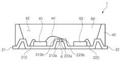
도 3은 도 2의 I-I를 따라 도시한 본 발명의 일 실시예에 따른 발광다이오드 패키지의 단면도.
도 4는 본 발명의 다른 실시예에 따른 발광다이오드 패키지를 도시한 평면도.1 is a plan view showing a conventional light emitting diode package.
2 is a plan view of a light emitting diode package according to an embodiment of the present invention;
3 is a cross-sectional view of a light emitting diode package according to an embodiment of the present invention, taken along II of FIG.
4 is a plan view illustrating a light emitting diode package according to another embodiment of the present invention.
이하, 첨부한 도면들을 참조하여 본 발명의 실시예를 상세히 설명하기로 한다. 다음에 소개되는 실시예는 당업자에게 본 발명의 사상이 충분히 전달될 수 있도록 하기 위해 예로서 제공되는 것이다. 따라서, 본 발명은 이하 설명되는 실시예들에 한정되지 않고 다른 형태로 구체화될 수도 있다. 그리고, 도면들에 있어서, 동일한 참조번호는 동일한 구성요소를 나타내며, 구성요소의 폭, 길이, 두께 등은 편의를 위하여 과장되어 표현될 수 있다.Hereinafter, embodiments of the present invention will be described in detail with reference to the accompanying drawings. The following embodiments are provided by way of example so that those skilled in the art can fully understand the spirit of the present invention. Therefore, the present invention is not limited to the embodiments described below, but may be embodied in other forms. In the drawings, the same reference numerals denote the same elements, and the width, length, thickness, and the like of the elements may be exaggerated for convenience.
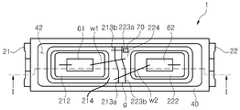
도 2는 본 발명의 일 실시예에 따른 발광다이오드 패키지를 도시한 평면도이고, 도 3은 도 2의 I-I를 따라 취해진 발광다이오드 패키지의 단면도이다.FIG. 2 is a plan view showing a light emitting diode package according to an embodiment of the present invention, and FIG. 3 is a sectional view of a light emitting diode package taken along line I-I of FIG.
도 2 및 도 3에 도시된 바와 같이, 본 실시예에 따른 발광다이오드 패키지(1)는 제1 및 제2 리드프레임(21, 22)과, 상기 제1 및 제2 리드프레임(21, 22)을 지지하는 대략 장방형의 패키지 몸체(40)와, 상기 제1 및 제2 리드프레임(21, 22)을 통해 전력을 인가받아 발광 동작되는 제1 및 제2 발광다이오드 칩(61, 62)을 포함한다.2 and 3, the
상기 패키지 몸체(40)는, 상기 제1 및 제2 리드프레임(21, 22)을 지지하도록, PPA와 같은 플라스틱 수지를 원료로 하는 사출 성형에 의해 만들어질 수 있다. 본 실시예에 있어서, 상기 패키지 몸체(40)의 상부에는 기다란 장방형의 캐비티(42)가 형성된다. 상기 캐비티(42)를 통해 상기 제1 및 제2 리드프레임(21, 22)의 상부 표면이 영역적으로 노출된다. 상기 캐비티(42) 내에서 상기 제1 및 제2 발광다이오드 칩(61, 62)이 상기 제1 및 제2 리드프레임(21, 22) 각각에 실장되어 있다. 투광성의 봉지재(80; 도 3에만 도시함)는 상기 제1 및 제2 발광다이오드 칩(61, 62)의 보호를 위해 상기 캐비티(42) 내에 채워져 형성된다.The
상기 제1 및 제2 리드프레임(21, 22) 각각은 패키지 몸체(40)의 내부로부터 양 측면으로 돌출 연장되어 발광 다이오드 패키지(1)의 외부 단자들을 형성한다. 이때, 외부 단자들을 구성하는 제1 및 제2 리드프레임(21, 22)의 외측 부분들 일부는 절곡된 구조에 의해 패키지 몸체(40)의 저면과 거의 동일 평면 상에 있게 된다.Each of the first and
상기 패키지 몸체(40)의 내측 캐비티(42) 영역에서는, 상기 제1 리드프레임(21)과 상기 제2 리드프레임(22)이 서로 이격되어 그들 사이에 하나의 갭(g)을 형성한다. 또한, 상기 제1 리드프레임(21)과 상기 제2 리드프레임(22)에는 제1 홀컵(212)과 제2 홀컵(222)이 각각 형성된다. 상기 제1 발광다이오드 칩(61)은 상기 제1 홀컵(212) 내에 위치하고 상기 제2 발광다이오드 칩(62)은 상기 제2 홀컵(222) 내에 위치한다. 상기 제1 홀컵(212)과 상기 제2 홀컵(222) 각각은 전술한 캐비티(42)의 길이 방향을 따라 기다란, 즉, 대략 직선인 짧은 변과 긴 변을 포함하는 대략 장방형의 형상을 갖는다. 또한, 상기 제1 및 제2 홀컵(212, 222)의 내측 벽면들은 반사 특성을 높이도록 경사면으로 이루어져 있다. 또한, 상기 제1 및 제2 홀컵(212, 222)의 저면은 상기 패키지 몸체(40)의 저면과 대략 동일 평면을 이루면서 외부로 노출된다.In the region of the
한편, 전술한 갭(g)은 대략 번개 모양으로 굴곡진 형상을 가지며, 이 굴곡진 형상에 의해, 상기 제1 및 제2 리드프레임(21, 22)의 내측 단부들 각각은 선행 단부(213a 또는 223a)와 그와 연결된 채 뒤로 처져 있는 후행 단부(213b 또는 223b)로 구분된다. 상기 선행 단부(213a 또는 223a)는 해당 리드프레임(21 또는 22)으로부터 이웃하는 다른 리드프레임(21 또는 22)을 향해 상기 후행 단부(213b 또는 223b)에 비해 더 돌출되어 있다. 제1 리드프레임(21)의 선행 단부(213a)는 제2 리드프레임(22)의 후행 단부(223b)와 인접하게 마주하며, 상기 제1 리드프레임(21)의 후행 단부(213b)는 상기 제2 리드프레임(22)의 선행 단부(223a)와 인접하게 마주한다.On the other hand, the above-mentioned gap g has a substantially curved shape, and the curved shape allows each of the inner ends of the first and
상기 선행 단부(213a 또는 223a)로 인해 그 부근 영역의 면적이 다른 단부 영역의 면적보다 확장되어 있다. 본 실시예에서, 이와 같이 확장된 영역은 발광다이오드 칩(61 또는 62)으로부터 이어진 본딩와이어(W1 또는 W2)가 본딩되는 와이어 본딩 영역으로 정해진다. 이에 따라, 전술한 제1 발광다이오드 칩(61)과 제2 발광다이오드 칩(62) 사이의 거리를 크게 늘리지 않고도, 제1 리드프레임(21)과 제2 리드프레임(22)의 내측 단부 부근에 충분히 확장된 와이어 본딩 영역을 보장할 수 있다.The area of the vicinity region extends beyond the area of the other end region due to the leading
전술한 구조에 의해, 상기 제1 및 제2 리드프레임(21, 22) 각각은 제1 홀컵(212)과 상기 갭(g) 사이 및 상기 제2 홀컵(222)과 상기 갭(g) 사이 각각에 인접 영역에 비해 더 큰 면적을 갖는 제1 확장 영역(214)과 제2 확장 영역(224)을 포함한다. 더 구체적으로, 상기 제1 리드프레임(21)의 제1 홀컵(212)과 상기 제1 리드프레임(21)의 선행 단부(213a) 사이에는 제1 확장 영역(214)이 제공되고, 상기 제2 리드프레임(22)의 제2 홀컵(222)과 상기 제2 리드프레임(22)의 선행 단부(223b) 사이에 제2 확장 영역(224)이 제공된다. 상기 제1 확장 영역(214)에는 상기 제2 리드프레임(22) 상의 제2 발광다이오드 칩(62)으로부터 이어진 본딩와이어(W2)의 일단부가 본딩되며, 상기 제2 확장 영역(224)에는 상기 제1 리드프레임(21) 상의 제1 발광다이오드 칩(61)으로부터 이어진 본딩와이어(W1)의 일단부가 본딩된다. 본 실시예에 있어서, 상기 제2 확장 영역(224)에는 제너다이오드(70)기 설치된다.The first and
리드프레임 상에 본딩와이어가 본딩되는 영역이 충분하지 못한 경우, 신뢰성 있는 와이어 본딩 작업을 할 수 없는데, 본 발명의 실시예에 따르면, 와이어 본딩을 할 수 없는 홀컵(212 또는 222)의 영역이 리드프레임(21 또는 22)에 큰 면적으로 존재함에도 불구하고, 전술한 제1 및 제2 확장 영역(214, 224)의 제공에 의해 충분한 면적의 와이어 본딩 영역을 보장한다. 또한, 상기 제1 및 제2 확장 영역(212, 214)의 제공을 통해, 상기 제1 및 제2 홀컵(212, 222)의 크기를 기존에 비해 증가시킬 수 있다. 홀컵의 크기 증가는 발광다이오드 패키지의 발광 효율을 높이는데 기여할 수 있다.A reliable wire bonding operation can not be performed when the area where the bonding wire is bonded on the lead frame is insufficient. According to the embodiment of the present invention, the area of the
상기 제1 확장 영역(214)과 상기 제2 확장 영역(224)의 다양한 배치가 고려될 수 있으나, 도 2에 잘 도시된 바와 같이, 상기 제1 확장 영역(214)과 상기 제2 확장 영역(224)은 대각선 방향으로 배치된다.As shown in FIG. 2, the
도 4는 본 발명의 다른 실시예에 따른 발광다이오드 패키지를 도시한 단면도이다.4 is a cross-sectional view illustrating a light emitting diode package according to another embodiment of the present invention.
도 4를 참조하면, 제1 리드프레임(21)과 제2 리드프레임(22)이 서로 이격되어 그들 사이에 하나의 갭(g)이 형성되되, 상기 갭(g)은 앞선 실시예와 달리 사선(inclined line) 형태를 갖는다. 사선 모양의 갭(g)에 의해 상기 제1 및 제2 리드프레임(21, 22)의 내측 단부들 각각은 선행 단부(213a 또는 223a)와 후행 단부(213b 또는 223b)를 갖지만, 상기 갭(g)과 상기 내측 단부들이 연속적인 직선 상에 있으므로 구분되지 않는다. 편의를 위해, 발광다이오드 패키지(1)의 중앙을 횡으로 가로지르는 가상의 기준선(L)을 기준으로 하여, 선행 단부(213a 또는 223a)와 후행 단부(213b 또는 223b)를 구분하기로 한다.Referring to FIG. 4, the
앞선 실시예와 마찬가지로, 상기 선행 단부(213a 또는 223a)는 해당 리드프레임(21 또는 22)으로부터 이웃하는 다른 리드프레임(21 또는 22)을 향해 상기 후행 단부(213b 또는 223b)에 비해 더 돌출되어 있다. 제1 리드프레임(21)의 선행 단부(213a)는 제2 리드프레임(22)의 후행 단부(223b)와 인접하게 마주하며, 상기 제1 리드프레임(21)의 후행 단부(213b)는 상기 제2 리드프레임(22)의 선행 단부(223a)와 인접하게 마주한다.The
또한, 상기 기준선(L)을 기준으로 하면, 상기 제1 리드프레임(21)의 제1 홀컵(212)과 상기 제1 리드프레임(21)의 선행 단부(213a) 사이에는 제1 확장 영역(214)이 제공되고, 상기 제2 리드프레임(22)의 제2 홀컵(222)과 상기 제2 리드프레임(22)의 선행 단부(223b) 사이에는 제2 확장 영역(224)이 제공된다. 상기 제1 확장 영역(214)에는 상기 제2 리드프레임(22) 상의 제2 발광다이오드 칩(62)으로부터 이어진 본딩와이어(W2)의 일단부가 본딩되며, 상기 제2 확장 영역(224)에는 상기 제1 리드프레임(21) 상의 제1 발광다이오드 칩(61)으로부터 이어진 본딩와이어(W1)의 일단부가 본딩된다. 본 실시예에 있어서, 상기 제2 확장 영역(224)에는 제너다이오드(70)가 설치된다.A
21: 제1 리드프레임 22: 제2 리드프레임
40: 패키지 몸체 42: 캐비티
61: 제1 발광다이오드 칩 62: 제2 발광다이오드 칩
212: 제1 홀컵 222: 제2 홀컵
214: 제1 확장 영역 224: 제2 확장 영역
213a, 223a: 선행 단부 213b, 223b: 후행 단부21: first lead frame 22: second lead frame
40: package body 42: cavity
61: first light emitting diode chip 62: second light emitting diode chip
212: first hole cup 222: second hole cup
214: first extended area 224: second extended area
213a, 223a: leading
Claims (15)
Translated fromKorean제2 홀컵이 형성되되, 상기 제1 리드프레임과 갭을 두고 대향되게 배치된 제2 리드프레임;
상기 제1 리드프레임 및 제2 리드프레임을 지지하는 패키지 몸체;
상기 제1 리드프레임 및 제2 리드프레임 각각으로부터 연장되어 상기 패키지 몸체의 측면으로부터 돌출되며, 상기 패키지 몸체의 저면과 동일 평면상에 위치하는 외부 단자들;
상기 제1 홀컵 내에 배치되는 제1 발광다이오드 칩; 및
상기 제2 홀컵 내에 배치되는 제2 발광다이오드 칩을 포함하며,
상기 제1 리드프레임은 상기 갭과 상기 제1 홀컵 사이에 인접 영역보다 넓으며, 와이어가 본딩되는 제1 확장 영역을 포함하고,
상기 제2 리드프레임은 상기 갭과 상기 제2 홀컵 사이에 인접 영역보다 넓으며, 와이어가 본딩되는 제2 확장 영역을 포함하고,
상기 제1 홀컵의 저면을 이루는 제1 리드프레임의 영역 및 제2 홀컵의 저면을 이루는 제2 리드프레임들의 영역은 상기 패키지 몸체의 저면과 동일 평면상에 위치하되, 외부로 노출되고,
상기 제1 확장 영역 및 제2 확장 영역은 각각 상기 제1 홀컵의 저면을 이루는 제1 리드프레임 영역 및 상기 제2 홀컵의 저면을 이루는 제2 리드프레임 영역보다 높은 곳에 배치되는 발광다이오드 패키지.
A first lead frame having a first hole cup formed therein;
A second lead frame having a second hole cup formed therein, the second lead frame facing the first lead frame with a gap therebetween;
A package body supporting the first lead frame and the second lead frame;
External terminals extending from each of the first lead frame and the second lead frame and protruding from a side surface of the package body, the external terminals being coplanar with the bottom surface of the package body;
A first light emitting diode chip disposed in the first hole cup; And
And a second light emitting diode chip disposed in the second hole cup,
Wherein the first lead frame includes a first extension region that is wider than an adjacent region between the gap and the first hole cup and to which the wire is bonded,
Wherein the second lead frame includes a second extension region that is wider than an adjacent region between the gap and the second hole cup and to which the wire is bonded,
The first lead frame region forming the bottom face of the first hole cup and the second lead frame region forming the bottom face of the second hole cup are positioned on the same plane as the bottom face of the package body,
Wherein the first extension region and the second extension region are disposed at a higher position than a first lead frame region forming the bottom surface of the first hole cup and a second lead frame region forming the bottom surface of the second hole cup, respectively.
상기 제1 리드프레임 및 제2 리드프레임을 지지하는 패키지 몸체;
상기 제1 리드프레임 및 제2 리드프레임 각각으로부터 연장되어 상기 패키지 몸체의 측면으로부터 돌출되며, 상기 패키지 몸체의 저면과 동일 평면상에 위치하는 외부 단자들; 및
상기 제1 리드프레임의 제1 홀컵에 실장되는 제1 발광다이오드 칩 및 상기 제2 리드프레임의 제2 홀컵에 실장되는 제2 발광다이오드 칩을 포함하며,
상기 내측 단부들 각각은 와이어 본딩 영역을 확장시키는 선행 단부와 그와 연결된 후행 단부를 포함하며,
상기 제1 발광다이오드 칩 및 상기 제2 발광다이오드 칩으로부터 이어진 본딩와이어 각각은 상기 선행 단부 부근의 확장된 영역에 본딩되고,
상기 제1 홀컵의 저면을 이루는 제1 리드프레임의 영역 및 제2 홀컵의 저면을 이루는 제2 리드프레임들의 영역은 상기 패키지 몸체의 저면과 동일 평면 상에 위치하되, 외부로 노출되고,
상기 선행 단부 부근의 확장된 영역은 제1 홀컵의 저면을 이루는 제1 리드프레임 영역 및 상기 제2 홀컵의 저면을 이루는 제2 리드프레임 영역보다 높은 곳에 배치되는 발광다이오드 패키지.
A second lead frame including a first lead frame and a second hole cup disposed adjacent to each other with the gap therebetween, the first lead frame including a first hole cup;
A package body supporting the first lead frame and the second lead frame;
External terminals extending from each of the first lead frame and the second lead frame and protruding from a side surface of the package body, the external terminals being coplanar with the bottom surface of the package body; And
A first light emitting diode chip mounted on a first hole cup of the first lead frame and a second light emitting diode chip mounted on a second hole cup of the second lead frame,
Each of the inner ends including a leading end extending a wire bonding region and a trailing end connected thereto,
Each of the bonding wires extending from the first light emitting diode chip and the second light emitting diode chip is bonded to the extended region near the leading end,
The first lead frame region forming the bottom face of the first hole cup and the second lead frame region forming the bottom face of the second hole cup are positioned on the same plane as the bottom face of the package body,
Wherein the extended region in the vicinity of the leading end is disposed at a higher level than a first lead frame region forming the bottom surface of the first hole cup and a second lead frame region forming the bottom surface of the second hole cup.
각각의 외부 단자는 상기 제1 리드프레임 및 제2 리드프레임의 절곡된 구조에 의해 상기 패키지 몸체의 저면과 동일 평면 상에 위치하는 발광다이오드 패키지.The method according to claim 1,
Wherein each of the external terminals is located on the same plane as the bottom surface of the package body by the bent structure of the first lead frame and the second lead frame.
각각의 외부 단자는 상기 제1 리드프레임 및 제2 리드프레임의 절곡된 구조에 의해 상기 패키지 몸체의 저면과 동일 평면상에 위치하는 발광다이오드 패키지.
The method of claim 6,
Wherein each of the external terminals is located on the same plane as the bottom surface of the package body by the bent structure of the first lead frame and the second lead frame.
Priority Applications (4)
| Application Number | Priority Date | Filing Date | Title |
|---|---|---|---|
| KR1020110018519AKR101812761B1 (en) | 2011-03-02 | 2011-03-02 | Light emitting diode package |
| TW101106630ATWI517458B (en) | 2011-03-02 | 2012-03-01 | LED package |
| US13/410,399US8994061B2 (en) | 2011-03-02 | 2012-03-02 | Light emitting diode package |
| CN201210052644.6ACN102655142B (en) | 2011-03-02 | 2012-03-02 | Light emission diode package member |
Applications Claiming Priority (1)
| Application Number | Priority Date | Filing Date | Title |
|---|---|---|---|
| KR1020110018519AKR101812761B1 (en) | 2011-03-02 | 2011-03-02 | Light emitting diode package |
Publications (2)
| Publication Number | Publication Date |
|---|---|
| KR20120099963A KR20120099963A (en) | 2012-09-12 |
| KR101812761B1true KR101812761B1 (en) | 2017-12-28 |
Family
ID=46730740
Family Applications (1)
| Application Number | Title | Priority Date | Filing Date |
|---|---|---|---|
| KR1020110018519AActiveKR101812761B1 (en) | 2011-03-02 | 2011-03-02 | Light emitting diode package |
Country Status (4)
| Country | Link |
|---|---|
| US (1) | US8994061B2 (en) |
| KR (1) | KR101812761B1 (en) |
| CN (1) | CN102655142B (en) |
| TW (1) | TWI517458B (en) |
Families Citing this family (18)
| Publication number | Priority date | Publication date | Assignee | Title |
|---|---|---|---|---|
| CN102403306B (en)* | 2010-09-10 | 2015-09-02 | 展晶科技(深圳)有限公司 | Package structure for LED |
| USD689029S1 (en)* | 2011-05-24 | 2013-09-03 | Lg Innotek Co., Ltd. | Portion of substrate for LED package |
| USD689030S1 (en)* | 2011-05-24 | 2013-09-03 | Lg Innotek Co., Ltd. | Portion of substrate for LED package |
| KR101957884B1 (en)* | 2012-05-14 | 2019-03-13 | 엘지이노텍 주식회사 | Light emitting device, manufactured method of the light emitting deviceand lighting apparatus |
| KR101886157B1 (en)* | 2012-08-23 | 2018-08-08 | 엘지이노텍 주식회사 | Light emitting deviceand lighting system |
| KR101896691B1 (en)* | 2012-10-11 | 2018-09-07 | 엘지이노텍 주식회사 | Light emitting device and lighting system |
| JP6102187B2 (en)* | 2012-10-31 | 2017-03-29 | 日亜化学工業株式会社 | Light emitting device package and light emitting device using the same |
| JP6107136B2 (en)* | 2012-12-29 | 2017-04-05 | 日亜化学工業株式会社 | LIGHT EMITTING DEVICE PACKAGE, LIGHT EMITTING DEVICE INCLUDING THE SAME, AND LIGHTING DEVICE EQUIPPED WITH THE LIGHT EMITTING DEVICE |
| JP6081229B2 (en)* | 2013-03-01 | 2017-02-15 | 株式会社東芝 | Semiconductor device, wireless device, and storage device |
| TWI506822B (en)* | 2013-03-25 | 2015-11-01 | I Chiun Precision Ind Co Ltd | Supporting base with asymmetrical circle wall for light-emitting diode chip |
| KR101976547B1 (en)* | 2013-04-29 | 2019-05-09 | 엘지이노텍 주식회사 | Light emitting device and lighting system |
| JP6261720B2 (en)* | 2013-05-17 | 2018-01-17 | オスラム オプト セミコンダクターズ ゲゼルシャフト ミット ベシュレンクテル ハフツングOsram Opto Semiconductors GmbH | Optoelectronic device and method of manufacturing optoelectronic device |
| CN104425694A (en)* | 2013-08-29 | 2015-03-18 | 展晶科技(深圳)有限公司 | Light emitting diode packaging structure and method for manufacturing thereof |
| JP6413412B2 (en)* | 2014-07-11 | 2018-10-31 | 日亜化学工業株式会社 | Semiconductor light emitting device and manufacturing method thereof |
| CN106876555A (en)* | 2017-04-17 | 2017-06-20 | 惠州雷曼光电科技有限公司 | Surface mount type LED support and adopting surface mounted LED device |
| JP6652117B2 (en)* | 2017-11-29 | 2020-02-19 | 日亜化学工業株式会社 | Resin package and light emitting device |
| KR20190127218A (en)* | 2018-05-04 | 2019-11-13 | 엘지이노텍 주식회사 | Semiconductor device package and light irradiation apparatus including the same |
| KR102816747B1 (en) | 2018-07-13 | 2025-06-10 | 듀폰스페셜티머터리얼스코리아 유한회사 | A plurality of host materials and organic electroluminescent device comprising the same |
Citations (1)
| Publication number | Priority date | Publication date | Assignee | Title |
|---|---|---|---|---|
| JP2009135381A (en)* | 2007-10-31 | 2009-06-18 | Sharp Corp | Chip component type LED and manufacturing method thereof |
Family Cites Families (4)
| Publication number | Priority date | Publication date | Assignee | Title |
|---|---|---|---|---|
| US6054716A (en)* | 1997-01-10 | 2000-04-25 | Rohm Co., Ltd. | Semiconductor light emitting device having a protecting device |
| KR101273083B1 (en)* | 2007-06-21 | 2013-06-10 | 엘지이노텍 주식회사 | Light Emitting device |
| KR101007131B1 (en)* | 2008-11-25 | 2011-01-10 | 엘지이노텍 주식회사 | Light emitting device package |
| US7923739B2 (en)* | 2009-06-05 | 2011-04-12 | Cree, Inc. | Solid state lighting device |
- 2011
- 2011-03-02KRKR1020110018519Apatent/KR101812761B1/enactiveActive
- 2012
- 2012-03-01TWTW101106630Apatent/TWI517458B/enactive
- 2012-03-02USUS13/410,399patent/US8994061B2/enactiveActive
- 2012-03-02CNCN201210052644.6Apatent/CN102655142B/enactiveActive
Patent Citations (1)
| Publication number | Priority date | Publication date | Assignee | Title |
|---|---|---|---|---|
| JP2009135381A (en)* | 2007-10-31 | 2009-06-18 | Sharp Corp | Chip component type LED and manufacturing method thereof |
Also Published As
| Publication number | Publication date |
|---|---|
| CN102655142B (en) | 2017-06-23 |
| CN102655142A (en) | 2012-09-05 |
| KR20120099963A (en) | 2012-09-12 |
| TW201238104A (en) | 2012-09-16 |
| TWI517458B (en) | 2016-01-11 |
| US8994061B2 (en) | 2015-03-31 |
| US20120223343A1 (en) | 2012-09-06 |
Similar Documents
| Publication | Publication Date | Title |
|---|---|---|
| KR101812761B1 (en) | Light emitting diode package | |
| JP5538233B2 (en) | Slim LED package | |
| CN103098217A (en) | LED Package with Efficient, Thermally Insulated Path | |
| TWI505519B (en) | Light-emitting diode light bar and manufacturing method thereof | |
| JP4976168B2 (en) | Light emitting device | |
| KR20110128592A (en) | LED Package | |
| US9159893B2 (en) | Light emitting device including lead having terminal part and exposed part, and method for manufacturing the same | |
| JP2009177112A (en) | Light emitting diode package | |
| JP2014049764A (en) | Side emission type light-emitting diode package and manufacturing method therefor | |
| JP3185994U (en) | Light emitting diode device and lead frame plate | |
| TWI509834B (en) | Light-emitting diode package structure and manufacturing method thereof | |
| KR101049487B1 (en) | Light emitting diode package | |
| KR101670951B1 (en) | Light emitting device | |
| KR101078028B1 (en) | Light emitting diode and lead frame thereof | |
| TWI531096B (en) | Side-emitting type light emitting diode package structure and manufacturing method thereof | |
| CN103682028A (en) | Light emitting diode package structure and manufacture method thereof | |
| CN102903825A (en) | Light emitting device | |
| KR101186649B1 (en) | Side view light emitting diode package | |
| TW201349600A (en) | Light-emitting diode and packaging method thereof | |
| KR20100003332A (en) | Led package with heat radiating structure | |
| TWI492424B (en) | Light emitting diode package structure | |
| KR20110080902A (en) | LED Package | |
| CN104425680A (en) | Light-emitting diode-packaging structure | |
| KR102436128B1 (en) | Light emitting diode package and manufacturing method of the same | |
| KR101380386B1 (en) | Light emitting diode package with high reliability |
Legal Events
| Date | Code | Title | Description |
|---|---|---|---|
| PA0109 | Patent application | St.27 status event code:A-0-1-A10-A12-nap-PA0109 | |
| P11-X000 | Amendment of application requested | St.27 status event code:A-2-2-P10-P11-nap-X000 | |
| P13-X000 | Application amended | St.27 status event code:A-2-2-P10-P13-nap-X000 | |
| R15-X000 | Change to inventor requested | St.27 status event code:A-3-3-R10-R15-oth-X000 | |
| R16-X000 | Change to inventor recorded | St.27 status event code:A-3-3-R10-R16-oth-X000 | |
| PG1501 | Laying open of application | St.27 status event code:A-1-1-Q10-Q12-nap-PG1501 | |
| PN2301 | Change of applicant | St.27 status event code:A-3-3-R10-R13-asn-PN2301 St.27 status event code:A-3-3-R10-R11-asn-PN2301 | |
| R18-X000 | Changes to party contact information recorded | St.27 status event code:A-3-3-R10-R18-oth-X000 | |
| A201 | Request for examination | ||
| PA0201 | Request for examination | St.27 status event code:A-1-2-D10-D11-exm-PA0201 | |
| P22-X000 | Classification modified | St.27 status event code:A-2-2-P10-P22-nap-X000 | |
| P22-X000 | Classification modified | St.27 status event code:A-2-2-P10-P22-nap-X000 | |
| E902 | Notification of reason for refusal | ||
| PE0902 | Notice of grounds for rejection | St.27 status event code:A-1-2-D10-D21-exm-PE0902 | |
| AMND | Amendment | ||
| E13-X000 | Pre-grant limitation requested | St.27 status event code:A-2-3-E10-E13-lim-X000 | |
| P11-X000 | Amendment of application requested | St.27 status event code:A-2-2-P10-P11-nap-X000 | |
| P13-X000 | Application amended | St.27 status event code:A-2-2-P10-P13-nap-X000 | |
| E601 | Decision to refuse application | ||
| PE0601 | Decision on rejection of patent | St.27 status event code:N-2-6-B10-B15-exm-PE0601 | |
| AMND | Amendment | ||
| E13-X000 | Pre-grant limitation requested | St.27 status event code:A-2-3-E10-E13-lim-X000 | |
| P11-X000 | Amendment of application requested | St.27 status event code:A-2-2-P10-P11-nap-X000 | |
| P13-X000 | Application amended | St.27 status event code:A-2-2-P10-P13-nap-X000 | |
| PX0901 | Re-examination | St.27 status event code:A-2-3-E10-E12-rex-PX0901 | |
| PX0701 | Decision of registration after re-examination | St.27 status event code:A-3-4-F10-F13-rex-PX0701 | |
| X701 | Decision to grant (after re-examination) | ||
| GRNT | Written decision to grant | ||
| PR0701 | Registration of establishment | St.27 status event code:A-2-4-F10-F11-exm-PR0701 | |
| PR1002 | Payment of registration fee | St.27 status event code:A-2-2-U10-U11-oth-PR1002 Fee payment year number:1 | |
| PG1601 | Publication of registration | St.27 status event code:A-4-4-Q10-Q13-nap-PG1601 | |
| PR1001 | Payment of annual fee | St.27 status event code:A-4-4-U10-U11-oth-PR1001 Fee payment year number:4 | |
| PR1001 | Payment of annual fee | St.27 status event code:A-4-4-U10-U11-oth-PR1001 Fee payment year number:5 | |
| PR1001 | Payment of annual fee | St.27 status event code:A-4-4-U10-U11-oth-PR1001 Fee payment year number:6 | |
| PR1001 | Payment of annual fee | St.27 status event code:A-4-4-U10-U11-oth-PR1001 Fee payment year number:7 | |
| PR1001 | Payment of annual fee | St.27 status event code:A-4-4-U10-U11-oth-PR1001 Fee payment year number:8 | |
| P22-X000 | Classification modified | St.27 status event code:A-4-4-P10-P22-nap-X000 | |
| P22-X000 | Classification modified | St.27 status event code:A-4-4-P10-P22-nap-X000 | |
| PR1001 | Payment of annual fee | St.27 status event code:A-4-4-U10-U11-oth-PR1001 Fee payment year number:9 |