KR101811663B1 - 후속 열처리 공정을 이용한 반도체 소자 제조 방법 및 그에 의해 제조된 반도체 소자 - Google Patents
후속 열처리 공정을 이용한 반도체 소자 제조 방법 및 그에 의해 제조된 반도체 소자Download PDFInfo
- Publication number
- KR101811663B1 KR101811663B1KR1020160039061AKR20160039061AKR101811663B1KR 101811663 B1KR101811663 B1KR 101811663B1KR 1020160039061 AKR1020160039061 AKR 1020160039061AKR 20160039061 AKR20160039061 AKR 20160039061AKR 101811663 B1KR101811663 B1KR 101811663B1
- Authority
- KR
- South Korea
- Prior art keywords
- layer
- semiconductor
- dielectric layer
- semiconductor layer
- metal
- Prior art date
- Legal status (The legal status is an assumption and is not a legal conclusion. Google has not performed a legal analysis and makes no representation as to the accuracy of the status listed.)
- Active
Links
- 239000004065semiconductorSubstances0.000titleclaimsabstractdescription149
- 238000000034methodMethods0.000titleclaimsdescription50
- 230000008569processEffects0.000titleclaimsdescription41
- 238000000137annealingMethods0.000titledescription14
- 238000004519manufacturing processMethods0.000titledescription8
- 229910052751metalInorganic materials0.000claimsabstractdescription43
- 239000002184metalSubstances0.000claimsabstractdescription43
- 239000001257hydrogenSubstances0.000claimsabstractdescription27
- 229910052739hydrogenInorganic materials0.000claimsabstractdescription27
- 239000007789gasSubstances0.000claimsabstractdescription8
- 125000004435hydrogen atomChemical class[H]*0.000claimsabstract3
- 229910052732germaniumInorganic materials0.000claimsdescription19
- GNPVGFCGXDBREM-UHFFFAOYSA-Ngermanium atomChemical group[Ge]GNPVGFCGXDBREM-UHFFFAOYSA-N0.000claimsdescription19
- QVGXLLKOCUKJST-UHFFFAOYSA-Natomic oxygenChemical compound[O]QVGXLLKOCUKJST-UHFFFAOYSA-N0.000claimsdescription8
- 239000001301oxygenSubstances0.000claimsdescription8
- 229910052760oxygenInorganic materials0.000claimsdescription8
- 238000000231atomic layer depositionMethods0.000claimsdescription7
- 238000000151depositionMethods0.000claimsdescription7
- 239000012535impuritySubstances0.000claimsdescription4
- 238000010438heat treatmentMethods0.000description22
- UFHFLCQGNIYNRP-UHFFFAOYSA-NHydrogenChemical compound[H][H]UFHFLCQGNIYNRP-UHFFFAOYSA-N0.000description20
- 239000000463materialSubstances0.000description12
- XLOMVQKBTHCTTD-UHFFFAOYSA-NZinc monoxideChemical compound[Zn]=OXLOMVQKBTHCTTD-UHFFFAOYSA-N0.000description9
- 229910010413TiO 2Inorganic materials0.000description7
- XUIMIQQOPSSXEZ-UHFFFAOYSA-NSiliconChemical compound[Si]XUIMIQQOPSSXEZ-UHFFFAOYSA-N0.000description6
- GWEVSGVZZGPLCZ-UHFFFAOYSA-NTitan oxideChemical compoundO=[Ti]=OGWEVSGVZZGPLCZ-UHFFFAOYSA-N0.000description6
- 229910052710siliconInorganic materials0.000description6
- 239000010703siliconSubstances0.000description6
- 239000010936titaniumSubstances0.000description6
- 230000004888barrier functionEffects0.000description5
- 238000005229chemical vapour depositionMethods0.000description5
- 230000007547defectEffects0.000description5
- 238000005516engineering processMethods0.000description4
- 150000002431hydrogenChemical class0.000description4
- 239000011787zinc oxideSubstances0.000description4
- 238000004458analytical methodMethods0.000description3
- 230000008859changeEffects0.000description3
- 230000000694effectsEffects0.000description3
- 150000002500ionsChemical class0.000description3
- 238000010030laminatingMethods0.000description3
- 239000000758substrateSubstances0.000description3
- 230000005641tunnelingEffects0.000description3
- 230000005428wave functionEffects0.000description3
- IJGRMHOSHXDMSA-UHFFFAOYSA-NAtomic nitrogenChemical compoundN#NIJGRMHOSHXDMSA-UHFFFAOYSA-N0.000description2
- 238000001505atmospheric-pressure chemical vapour depositionMethods0.000description2
- 238000000277atomic layer chemical vapour depositionMethods0.000description2
- 150000001875compoundsChemical class0.000description2
- 230000008021depositionEffects0.000description2
- 230000005669field effectEffects0.000description2
- 238000009413insulationMethods0.000description2
- 238000004518low pressure chemical vapour depositionMethods0.000description2
- CPLXHLVBOLITMK-UHFFFAOYSA-Nmagnesium oxideInorganic materials[Mg]=OCPLXHLVBOLITMK-UHFFFAOYSA-N0.000description2
- 239000000395magnesium oxideSubstances0.000description2
- AXZKOIWUVFPNLO-UHFFFAOYSA-Nmagnesium;oxygen(2-)Chemical compound[O-2].[Mg+2]AXZKOIWUVFPNLO-UHFFFAOYSA-N0.000description2
- 230000035515penetrationEffects0.000description2
- 238000000623plasma-assisted chemical vapour depositionMethods0.000description2
- 229910021332silicideInorganic materials0.000description2
- FVBUAEGBCNSCDD-UHFFFAOYSA-Nsilicide(4-)Chemical compound[Si-4]FVBUAEGBCNSCDD-UHFFFAOYSA-N0.000description2
- 229910018072Al 2 O 3Inorganic materials0.000description1
- 229910002616GeOxInorganic materials0.000description1
- 229910004298SiO 2Inorganic materials0.000description1
- VYPSYNLAJGMNEJ-UHFFFAOYSA-NSilicium dioxideChemical compoundO=[Si]=OVYPSYNLAJGMNEJ-UHFFFAOYSA-N0.000description1
- 230000005540biological transmissionEffects0.000description1
- 230000015556catabolic processEffects0.000description1
- 230000000295complement effectEffects0.000description1
- 238000006731degradation reactionMethods0.000description1
- 238000005530etchingMethods0.000description1
- 238000002474experimental methodMethods0.000description1
- 239000003574free electronSubstances0.000description1
- YBMRDBCBODYGJE-UHFFFAOYSA-Ngermanium dioxideChemical compoundO=[Ge]=OYBMRDBCBODYGJE-UHFFFAOYSA-N0.000description1
- 230000005484gravityEffects0.000description1
- CJNBYAVZURUTKZ-UHFFFAOYSA-Nhafnium(iv) oxideChemical compoundO=[Hf]=OCJNBYAVZURUTKZ-UHFFFAOYSA-N0.000description1
- MRELNEQAGSRDBK-UHFFFAOYSA-Nlanthanum(3+);oxygen(2-)Chemical compound[O-2].[O-2].[O-2].[La+3].[La+3]MRELNEQAGSRDBK-UHFFFAOYSA-N0.000description1
- 150000002739metalsChemical class0.000description1
- 230000000116mitigating effectEffects0.000description1
- 238000012986modificationMethods0.000description1
- 230000004048modificationEffects0.000description1
- 229910052757nitrogenInorganic materials0.000description1
- TWNQGVIAIRXVLR-UHFFFAOYSA-Noxo(oxoalumanyloxy)alumaneChemical compoundO=[Al]O[Al]=OTWNQGVIAIRXVLR-UHFFFAOYSA-N0.000description1
- SIWVEOZUMHYXCS-UHFFFAOYSA-Noxo(oxoyttriooxy)yttriumChemical compoundO=[Y]O[Y]=OSIWVEOZUMHYXCS-UHFFFAOYSA-N0.000description1
- UFQXGXDIJMBKTC-UHFFFAOYSA-NoxostrontiumChemical compound[Sr]=OUFQXGXDIJMBKTC-UHFFFAOYSA-N0.000description1
- RVTZCBVAJQQJTK-UHFFFAOYSA-Noxygen(2-);zirconium(4+)Chemical compound[O-2].[O-2].[Zr+4]RVTZCBVAJQQJTK-UHFFFAOYSA-N0.000description1
- 238000000206photolithographyMethods0.000description1
- CHWRSCGUEQEHOH-UHFFFAOYSA-Npotassium oxideChemical compound[O-2].[K+].[K+]CHWRSCGUEQEHOH-UHFFFAOYSA-N0.000description1
- 229910001950potassium oxideInorganic materials0.000description1
- 229910052814silicon oxideInorganic materials0.000description1
- 238000012995silicone-based technologyMethods0.000description1
- 238000001228spectrumMethods0.000description1
- OGIDPMRJRNCKJF-UHFFFAOYSA-Ntitanium oxideInorganic materials[Ti]=OOGIDPMRJRNCKJF-UHFFFAOYSA-N0.000description1
- 238000007740vapor depositionMethods0.000description1
- 239000011701zincSubstances0.000description1
- 229910001928zirconium oxideInorganic materials0.000description1
Images


Classifications
- H—ELECTRICITY
- H01—ELECTRIC ELEMENTS
- H01L—SEMICONDUCTOR DEVICES NOT COVERED BY CLASS H10
- H01L21/00—Processes or apparatus adapted for the manufacture or treatment of semiconductor or solid state devices or of parts thereof
- H01L21/70—Manufacture or treatment of devices consisting of a plurality of solid state components formed in or on a common substrate or of parts thereof; Manufacture of integrated circuit devices or of parts thereof
- H01L21/71—Manufacture of specific parts of devices defined in group H01L21/70
- H01L21/768—Applying interconnections to be used for carrying current between separate components within a device comprising conductors and dielectrics
- H01L21/76801—Applying interconnections to be used for carrying current between separate components within a device comprising conductors and dielectrics characterised by the formation and the after-treatment of the dielectrics, e.g. smoothing
- H01L21/76822—Modification of the material of dielectric layers, e.g. grading, after-treatment to improve the stability of the layers, to increase their density etc.
- H01L21/76828—Modification of the material of dielectric layers, e.g. grading, after-treatment to improve the stability of the layers, to increase their density etc. thermal treatment
- H—ELECTRICITY
- H01—ELECTRIC ELEMENTS
- H01L—SEMICONDUCTOR DEVICES NOT COVERED BY CLASS H10
- H01L21/00—Processes or apparatus adapted for the manufacture or treatment of semiconductor or solid state devices or of parts thereof
- H01L21/02—Manufacture or treatment of semiconductor devices or of parts thereof
- H01L21/02104—Forming layers
- H01L21/02107—Forming insulating materials on a substrate
- H01L21/02225—Forming insulating materials on a substrate characterised by the process for the formation of the insulating layer
- H01L21/02227—Forming insulating materials on a substrate characterised by the process for the formation of the insulating layer formation by a process other than a deposition process
- H01L21/02255—Forming insulating materials on a substrate characterised by the process for the formation of the insulating layer formation by a process other than a deposition process formation by thermal treatment
- H—ELECTRICITY
- H01—ELECTRIC ELEMENTS
- H01L—SEMICONDUCTOR DEVICES NOT COVERED BY CLASS H10
- H01L21/00—Processes or apparatus adapted for the manufacture or treatment of semiconductor or solid state devices or of parts thereof
- H01L21/02—Manufacture or treatment of semiconductor devices or of parts thereof
- H01L21/02104—Forming layers
- H01L21/02107—Forming insulating materials on a substrate
- H01L21/02225—Forming insulating materials on a substrate characterised by the process for the formation of the insulating layer
- H01L21/0226—Forming insulating materials on a substrate characterised by the process for the formation of the insulating layer formation by a deposition process
- H01L21/02263—Forming insulating materials on a substrate characterised by the process for the formation of the insulating layer formation by a deposition process deposition from the gas or vapour phase
- H01L21/02271—Forming insulating materials on a substrate characterised by the process for the formation of the insulating layer formation by a deposition process deposition from the gas or vapour phase deposition by decomposition or reaction of gaseous or vapour phase compounds, i.e. chemical vapour deposition
- H01L21/0228—Forming insulating materials on a substrate characterised by the process for the formation of the insulating layer formation by a deposition process deposition from the gas or vapour phase deposition by decomposition or reaction of gaseous or vapour phase compounds, i.e. chemical vapour deposition deposition by cyclic CVD, e.g. ALD, ALE, pulsed CVD
- H—ELECTRICITY
- H01—ELECTRIC ELEMENTS
- H01L—SEMICONDUCTOR DEVICES NOT COVERED BY CLASS H10
- H01L21/00—Processes or apparatus adapted for the manufacture or treatment of semiconductor or solid state devices or of parts thereof
- H01L21/02—Manufacture or treatment of semiconductor devices or of parts thereof
- H01L21/04—Manufacture or treatment of semiconductor devices or of parts thereof the devices having potential barriers, e.g. a PN junction, depletion layer or carrier concentration layer
- H01L21/18—Manufacture or treatment of semiconductor devices or of parts thereof the devices having potential barriers, e.g. a PN junction, depletion layer or carrier concentration layer the devices having semiconductor bodies comprising elements of Group IV of the Periodic Table or AIIIBV compounds with or without impurities, e.g. doping materials
- H01L21/28—Manufacture of electrodes on semiconductor bodies using processes or apparatus not provided for in groups H01L21/20 - H01L21/268
- H01L21/28008—Making conductor-insulator-semiconductor electrodes
- H01L21/28017—Making conductor-insulator-semiconductor electrodes the insulator being formed after the semiconductor body, the semiconductor being silicon
- H01L21/28158—Making the insulator
- H01L21/28167—Making the insulator on single crystalline silicon, e.g. using a liquid, i.e. chemical oxidation
- H01L21/28194—Making the insulator on single crystalline silicon, e.g. using a liquid, i.e. chemical oxidation by deposition, e.g. evaporation, ALD, CVD, sputtering, laser deposition
- H—ELECTRICITY
- H01—ELECTRIC ELEMENTS
- H01L—SEMICONDUCTOR DEVICES NOT COVERED BY CLASS H10
- H01L21/00—Processes or apparatus adapted for the manufacture or treatment of semiconductor or solid state devices or of parts thereof
- H01L21/02—Manufacture or treatment of semiconductor devices or of parts thereof
- H01L21/04—Manufacture or treatment of semiconductor devices or of parts thereof the devices having potential barriers, e.g. a PN junction, depletion layer or carrier concentration layer
- H01L21/18—Manufacture or treatment of semiconductor devices or of parts thereof the devices having potential barriers, e.g. a PN junction, depletion layer or carrier concentration layer the devices having semiconductor bodies comprising elements of Group IV of the Periodic Table or AIIIBV compounds with or without impurities, e.g. doping materials
- H01L21/30—Treatment of semiconductor bodies using processes or apparatus not provided for in groups H01L21/20 - H01L21/26
- H01L21/324—Thermal treatment for modifying the properties of semiconductor bodies, e.g. annealing, sintering
- H—ELECTRICITY
- H01—ELECTRIC ELEMENTS
- H01L—SEMICONDUCTOR DEVICES NOT COVERED BY CLASS H10
- H01L21/00—Processes or apparatus adapted for the manufacture or treatment of semiconductor or solid state devices or of parts thereof
- H01L21/67—Apparatus specially adapted for handling semiconductor or electric solid state devices during manufacture or treatment thereof; Apparatus specially adapted for handling wafers during manufacture or treatment of semiconductor or electric solid state devices or components ; Apparatus not specifically provided for elsewhere
- H01L21/67005—Apparatus not specifically provided for elsewhere
- H01L21/67011—Apparatus for manufacture or treatment
- H01L21/67098—Apparatus for thermal treatment
- H—ELECTRICITY
- H01—ELECTRIC ELEMENTS
- H01L—SEMICONDUCTOR DEVICES NOT COVERED BY CLASS H10
- H01L2924/00—Indexing scheme for arrangements or methods for connecting or disconnecting semiconductor or solid-state bodies as covered by H01L24/00
- H01L2924/01—Chemical elements
- H01L2924/01001—Hydrogen [H]
Landscapes
- Engineering & Computer Science (AREA)
- Manufacturing & Machinery (AREA)
- Physics & Mathematics (AREA)
- Condensed Matter Physics & Semiconductors (AREA)
- General Physics & Mathematics (AREA)
- Computer Hardware Design (AREA)
- Microelectronics & Electronic Packaging (AREA)
- Power Engineering (AREA)
- Chemical Kinetics & Catalysis (AREA)
- Chemical & Material Sciences (AREA)
- Crystallography & Structural Chemistry (AREA)
- General Chemical & Material Sciences (AREA)
- Insulated Gate Type Field-Effect Transistor (AREA)
- Thin Film Transistor (AREA)
Abstract
Description
본 발명은 반도체 구조와, 이를 포함하는 반도체 소자 및 그 제조방법에 관한 것으로, 보다 구체적으로 반도체층 위에 형성되는 유전체층을 수소(H2)로 열처리하여 낮은 접촉 저항을 구현하는 반도체 구조와, 이를 포함하는 반도체 소자 및 그 제조방법에 관한 것이다.
반도체 CMOS(Complementary metal-oxide-semiconductor) 기술의 기본 소자가 되는 FET(Field Effect Transistor)는 스위칭 소자로서 온-오프를 위한 게이트(gate)와 전류 전달을 위한 소스(source) 및 드레인(drain)으로 구성된다.
상기 FET 소자가 동작할 때, 높은 성능과 낮은 전력 특성을 동시에 확보하기 위해서는 소스 및 드레인이 가지는 금속 전극과 반도체 사이의 접촉 저항(Contact Resistance)을 감소시키는 것이 중요하다.
소스 및 드레인 영역은 일반적으로 금속-반도체(metal-semiconductor) 형태로 구성되어 있으며 현재 CMOS 기술에서 주로 사용되고 있는 반도체 물질인 실리콘 (Si)의 경우 금속과 반도체의 화합물 형태인 실리사이드(silicide) 공정을 사용하여 소스/드레인의 접촉 저항을 낮출 수 있다.
그러나 실리사이드 공정은 비교적 높은 공정 온도와 고온에서의 상변화(phase change) 문제 등으로 인해 차세대 반도체 기술인 3차원 집적회로 기술이나 저마늄(Ge) 등의 차세대 채널 물질과의 공정 호환성이 좋지 않다.
또한, 반도체 CMOS 기술에서 현재 사용되고 있는 채널 물질인 실리콘 기반 기술의 경우, 소자의 지속적인 소형화에 따라 물리적 한계에 직면하였으며, 이를 대체할 차세대 채널 물질로 실리콘에 비해 높은 전자/정공 이동도(carrier mobility)와 실리콘 공정과의 호환성이 높은 저마늄이 각광받고 있다.
그러나 저마늄 FET는 n형 소스/드레인 영역의 금속-반도체 접합에서 발생하는 극심한 페르미 레벨 피닝 현상으로 인하여 높은 소스/드레인 접촉 저항을 갖는 문제점이 있다.
저마늄과 같은 반도체 물질에서 페르미 레벨 피닝 현상을 일으키는 요인은 크게 두 가지로 분류할 수 있는데 금속과의 접합 과정에서 발생하는 MIGS(Metal-Induced Gap States)와 금속-반도체 또는 유전체-반도체 계면에 존재하는 결함에 의해 생기는 경계면 상태(interface states)이다.
따라서, 저마늄 기반의 CMOS 공정에서 MIGS 및 경계면 상태(interface states)를 감소시키고 접촉 저항을 감소시킬 수 있는 기술이 요구된다.
본 발명의 목적은 소스 및 드레인이 형성되는 반도체층에 유전체층을 형성하고, 유전체층을 수소 열처리하여 낮은 접촉 저항을 구현하는 반도체 구조와, 이를 포함하는 반도체 소자 및 그 제조방법을 제공하는 것이다.
본 발명의 실시 예에 따른 반도체 구조는 반도체층; 상기 반도체층의 상부에 형성된 유전체층; 및 상기 유전체층 상부에 형성된 금속층;을 포함하고, 상기 반도체층에서 상기 유전체층과 접합되는 표면 및 상기 유전체층이 수소(H2) 가스를 이용하여 열처리된 것을 특징으로 한다.
본 발명의 실시 예에 따른 반도체 소자는 제1 반도체층; 상기 제1 반도체층의 표면의 소스 및 드레인 영역에 형성된 제2 반도체층; 상기 제2 반도체층 위에 형성된 유전체층; 및 상기 유전체층 위에 형성된 금속층;을 포함하고, 상기 제2 반도체층에서 상기 유전체층과 접합되는 표면 및 상기 유전체층이 수소(H2) 가스를 이용하여 열처리된 것을 특징으로 한다.
본 발명의 실시 예에 따른 반도체 소자 제조 방법은 반도체층을 마련하는 단계; 상기 반도체층의 표면에 소스 및 드레인을 형성하는 단계; 상기 소스 및 드레인의 상부에 유전체층을 형성하는 단계; 상기 소스 및 상기 드레인의 표면 및 상기 유전체층을 수소 열처리하는 단계; 및 상기 수소 열처리된 상기 유전체층의 상부에 금속층을 증착하는 단계;를 포함한다.
본 발명의 일 실시예에 따르면, 반도체층 표면 및 반도체층 위에 존재하는 유전체층 내부를 수소 열처리하여 낮은 접촉 저항을 구현하는 반도체 구조를 제공할 수 있다.
또한, 본 발명의 일 실시예에 따르면, 수소 열처리 공정을 반도체층 위에 유전체층을 증착한 후, 유전체층 위에 금속층을 증착하기 전에 수행함으로써, 반도체층(특히, 소스 및 드레인)의 표면에 존재하는 표면 결함을 감소시키고 유전체층-반도체층 계면에 존재하는 경계면 상태(interface states)를 줄여, 페르미 레벨 피닝을 완화하여 접촉 저항을 낮춤으로써 반도체 소자의 특성을 향상시킬 수 있다.
또한, 동일한 공정을 통해 유전체층의 전기전도도를 향상하여 반도체 소자의 접촉 저항을 낮출 수 있는 효과가 있다.
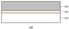
도 1은 본 발명의 일 실시예에 따른 반도체 구조를 개략적으로 도시한 단면도이다.
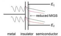
도 2는 금속과 반도체 사이의 MIGS(Metal Induced Gap States) 효과를 나타낸 것이다.
도 3은 금속, 유전체층, 및 반도체 구조에서의 MIGS(Metal Induced Gap States) 효과의 변화를 나타낸 것이다.
도 4는 후속 수소 열처리한 것과 후속 수소 열처리하지 않았을 때의 유전체층 및 반도체층의 XPS 분석결과를 비교하여 도시한 그래프이다.
도 5는 본 발명의 다른 실시예에 따른 반도체 소자를 개략적으로 도시한 단면도이다.
도 6은 본 발명의 일 실시예에 따른 반도체 구조 제조방법을 개략적으로 도시한 흐름도이다.
도 7은 후속 수소 열처리한 것과 후속 수소 열처리하지 않았을 때의 전압에 따른 전류 밀도의 변화를 비교하여 도시한 그래프이다.
도 8은 후속 수소 열처리한 것과 후속 수소 열처리하지 않았을 때의 접촉 저항 변화를 비교하여 도시한 그래프이다.
본 발명에 관한 구체적인 내용의 설명에 앞서 이해의 편의를 위해 본 발명이 해결하고자 하는 과제의 해결 방안의 개요 혹은 기술적 사상의 핵심을 우선 제시한다.
이하 첨부된 도면을 참조하여 본 발명이 속하는 기술 분야에서 통상의 지식을 가진 자가 본 발명을 용이하게 실시할 수 있는 실시 예를 상세히 설명한다. 그러나 이들 실시예는 본 발명을 보다 구체적으로 설명하기 위한 것으로, 본 발명의 범위가 이에 의하여 제한되지 않는다는 것은 당업계의 통상의 지식을 가진 자에게 자명할 것이다.
본 발명이 해결하고자 하는 과제의 해결 방안을 명확하게 하기 위한 발명의 구성을 본 발명의 바람직한 실시예에 근거하여 첨부 도면을 참조하여 상세히 설명하되, 당해 도면에 대한 설명시 필요한 경우 다른 도면의 구성요소를 인용할 수 있음을 미리 밝혀둔다. 아울러 본 발명의 바람직한 실시 예에 대한 동작 원리를 상세하게 설명함에 있어 본 발명과 관련된 공지 기능 혹은 구성에 대한 구체적인 설명 그리고 그 이외의 제반 사항이 본 발명의 요지를 불필요하게 흐릴 수 있다고 판단되는 경우, 그 상세한 설명을 생략한다.
도 1은 본 발명의 일 실시예에 따른 반도체 구조를 개략적으로 도시한 단면도이다.
도 1을 참조하면, 본 발명의 일 실시예에 따른 반도체 구조는 반도체층(110), 유전체층(120), 및 금속층(130)을 포함한다.
반도체층(110)은 4족 화합물(예를 들어, 실리콘, 저마늄 등)로 형성될 수 있다. 바람직하게는 반도체층(110)은 저마늄(Ge)으로 형성될 수 있다.
금속층(130)은 반도체 소자의 소스 또는 드레인을 형성할 수 있다.
유전체층(120)은 반도체층(110)과 금속층(130) 사이에 형성되며, 유전체층(120)은 원자층 증착 공정(ALD)을 통해 형성될 수 있다. 원자층 증착 공정의 경우, 복잡한 형상의 3차원 구조에서도 뛰어난 균일도를 가지는 나노 두께의 박막 증착이 가능하기 때문에 나노급 반도체 소자 제조의 적합하다. 유전체층(120)의 두께는 1nm 내지 2nm일 수 있다.
금속층(130)과 반도체층(110) 사이에 유전체층(120)을 형성함으로써 금속층(130)과 반도체층(110)이 직접 접촉할 때 발생하는 문제점을 해결할 수 있다.
반도체층(110)에 금속층(130)을 직접 접촉하는 경우, 금속의 일함수 (workfunction)과 관계없이 금속의 페르미 레벨(Fermi level)이 반도체 밴드갭 (bandgap) 내의 특정 에너지 준위 근처에 고정되는 페르미 레벨 피닝(Fermi-level pinning) 현상이 발생한다.
도 2a를 참조하면, 예를 들어, 저마늄 반도체층(110)의 경우 페르미 레벨 피닝 현상이 심하게 발생하여 금속-저마늄 접촉에서 금속의 페르미 레벨이 저마늄의 가전자대(valence band) 끝에 고정되고, 0.55eV의 큰 전자 쇼트키 장벽(electron Schottky barrier)이 형성되어 접촉저항이 증가하는 문제점이 발생한다. 즉, 실리콘, 저마늄과 같은 반도체에서 페르미 레벨 피닝 현상에 의해 생성된 큰 쇼트키 장벽은 n형 FET의 소스/드레인 접합에서 쇼트키 접합을 형성하여 높은 소스/드레인 접촉 저항과 성능 열화를 초래한다.
도 2b는 금속-반도체 접촉에서 페르미 레벨 피닝 현상을 일으키는 금속 내 전자들의 파동 함수 침투로 인해 반도체 밴드갭 내에 생기는 MIGS(metal-induced gap states)를 도시한다.
본 발명에 따른 금속-유전체-반도체(MIS, Metal-Inter layer-Semiconductor) 구조는 실리콘, 저마늄과 같은 반도체 물질에서 페르미 레벨 피닝 현상을 일으키는 금속 내 전자들의 파동 함수 침투로 인해 반도체 밴드갭 내에 생기는 MIGS(metal-induced gap states)를 물리적으로 감소시켜 페르미 레벨 피닝 현상을 완화할 수 있는 구조이다.
도 3a를 참조하면, 반도체층(110)과 금속층(130) 사이에 수 nm의 두께를 갖는 유전체층(120)을 형성하는 경우, 금속 내부에 존재하는 전자의 파동 함수가 미치는 영향을 물리적으로 감소시킴으로써 MIGS를 줄이고 페르미 레벨 피닝 현상을 감소시킬 수 있다.
유전체층(120)은 산화물층일 수 있다. 예를 들어, 유전체층(120)은 티타늄옥사이드(TiO2), 징크옥사이드(ZnO), 지르코늄옥사이드(ZrO2), 실리콘옥사이드(SiO2), 하프늄옥사이드(HfO2), 란타늄옥사이드(La2O3), 알루미늄옥사이드(Al2O3), 이트륨옥사이드(Y2O3), 마그네슘옥사이드(MgO), 게르마늄옥사이드(GeO2), 스트론튬옥사이드(SrO) 및 루테슘옥사이드(Lu2O3) 중에서 어느 하나의 산화물로 이루어질 수 있다.
바람직하게는 유전체층(120)은 반도체층(110)과의 전자 친화도(electron affinity) 값이 비슷한 물질로 구성될 수 있다. 예를 들어, 반도체층(110)이 저마늄(Ge, 전자친화도 ~4.0eV)으로 형성된 경우, 유전체층(120)은 저마늄과 전자친화도가 비슷한 물질인 티타늄옥사이드(TiO2, 전자친화도 ~4.2eV) 또는 징크옥사이드(ZnO, 전자친화도 ~4.2eV) 등으로 형성할 수 있다.
도 3b를 참조하면, 실리콘, 저마늄과의 전자 친화도 값이 비슷한 물질로 유전체층(120)을 형성하는 경우, 페르미 레벨 피닝 현상을 완화하여 쇼트키 장벽을 효과적으로 낮출 수 있을 뿐만 아니라 전자의 터널링 장벽(tunneling barrier)를 최소화하여 접촉 저항을 크게 낮출 수 있다.
또한, 유전체층(120)은 전기 전도도가 높은 물질로 구성될 수 있다. 예를 들어, 산화막 유전체층(120)은 산소 공백(oxygen vacancy)을 포함하는 산화물층일 수 있다. 즉, 유전체층(120)은 산소 공백을 포함하는 물질(예를 들어, TiO2-x, Zn1+yO 등)을 포함할 수 있다.
도 3c를 참조하면, 유전체층(120)의 전기 전도도가 증가할 경우, 도 3b에 비해 유전체층(120)의 터널링 두께가 현저하게 감소하는 효과가 있으며, 따라서 접촉 저항을 크게 낮출 수 있다. 또한, 유전체층(120) 내부에 발생하는 전기적 포텐셜(potential)에 의해 추가적인 쇼트키 장벽의 감소를 가져와 해당 구조의 접촉 저항을 더욱 낮출 수 있는 효과가 있다.
유전체층(120)은 후속 수소 열처리(post H2 thermal annealing) 공정이 수행될 수 있다. 구체적으로 반도체층(110)에 유전체층(120, 예를 들어, TiO2)을 증착하고, 350℃ 내지 450℃, 바람직하게는 400℃에서 수소 열처리 공정을 진행할 경우, 유전체층(120)의 전기전도도가 증가하고, 유전체층(120)과 반도체층(110) 사이에 존재하는 경계면 상태(interface state)가 감소하는 효과가 있으며, 따라서 매우 낮은 접촉 저항을 구현할 수 있다.
H2의 경우 수 nm 수준으로 매우 얇은 산화막 유전체층(120, 예를 들어, TiO2, ZnO 등)에 침투하여 층 내부에 산소 공백(oxygen vacancy)을 만드는데, 이는 산화막 유전체층(120)에서 도너 준위(donor level)로 작용하게 된다. 도너 준위 역할을 하는 산소 공백에 의해 산화막 유전체층(120) 내부에 자유 전자가 생기게 되고 이는 유전체의 전기 전도도를 높이는 역할을 한다.
도 4a는 후속 H2 열처리 공정 전과 후의 TiO2 층의 XPS 분석 결과를 비교하여 도시한 그래프이다. 도 4a를 참조하면, H2 열처리 공정 이후 Ti 2p 스팩트럼의 음성 편이(negative shift)를 통해 산소와의 결합이 일부 끊어진 Ti3+의 비중이 증가하는 것을 확인할 수 있으며 도너 역할을 하는 산소 공백의 존재를 확인할 수 있다.
반도체 표면에서 경계면 상태(interface states)를 만드는 요인은 반도체의 댕글링 본드(dangling bond) 등과 같은 표면 결함이나 산화막 형태의 유전체와 접합했을 때 형성되는 불완전한 반도체 산화막(예를 들어, GeOx) 등이 있다. 후속 H2 열처리 공정에서 H2는 유전체 층을 뚫고 들어가 유전체-반도체 사이에 존재하는 불완전한 산화 결합을 끊고 반도체 표면과 결합함으로써 유전체-반도체 계면의 경계면 상태(interface states)가 효과적으로 감소하는 효과가 있다.
도 4b는 후속 H2 열처리 공정 전과 후의 반도체층(Ge 기판)의 XPS 분석 결과를 비교하여 도시한 그래프이다. 도 4b를 참조하면, H2 열처리 공정 이후 반도체층(Ge)과 유전체층(TiO2) 사이에 존재하던 Ge-O의 결합이 상당 부분 사라지는 것을 볼 수 있으며, 이를 통해 H2 열처리 공정이 유전체-반도체 계면에 존재하는 경계면 상태(interface states)를 효과적으로 감소시키는 것을 확인할 수 있다.
반도체 FET (특히, 저마늄 기반의 n형 FET)의 소스/드레인 공정에 본 발명에서 제안하는 금속-유전체-반도체 구조 및 후속 수소 열처리 공정을 도입할 경우 MIGS 및 경계면 상태(interface states)를 효과적으로 감소시켜 페르미 레벨 피닝 현상을 감소시킬 뿐만 아니라 유전체의 전기 전도도를 향상시켜 전자의 터널링 확률을 증가시킴으로써 저저항의 오믹 소스/드레인 형성이 가능하다.
도 5는 소스와 드레인에 본 발명에 따른 금속-유전체-반도체 구조를 도입한 반도체 소자(예를 들어, MOSFET)를 개략적으로 도시한 단면도이다.
본 발명의 실시예에 따른 금속-유전체-반도체 구조는 일반적인 MOSFET(metal-oxide-semiconductor field-effect transistor) 구조에 국한하는 것이 아니라, 소스와 드레인이 필요한 반도체 소자 (예를 들면 FinFET, HEMT, JFET과 같은 트랜지스터)에 적용이 가능하다.
도 5를 참조하면, 본 실시예에 따른 반도체 소자는, 제1 반도체층(211) 및 제2 반도체층(212)을 포함하는 반도체층(210), 제1 반도체층 위에 형성되는 유전체층(220), 유전체층(220) 위에 형성되는 금속 전극(230), 제2 반도체층의 사이를 덮도록 형성되는 게이트 및 게이트 전극을 포함한다.
제2 반도체층(212)은 이온이 고농도로 도핑된 소스/드레인 영역으로, 반도체층(210)의 종류 및 반도체 소자의 종류 등에 따라 다양한 불순물 이온이 도핑되어 형성될 수 있다. 본 실시예에 따른 반도체 소자의 반도체층(210)은 저마늄(Ge)을 이용할 수 있으며, 또한, 소스 및 드레인(제2 반도체층, 212)은 n형의 불순물을 주입하여 형성될 수 있다.
금속 전극(230)은 반도체층(210)의 상부에 절연층을 형성한 후, 일부를 식각하고 유전체층(220)을 형성한 후, 금속을 증착하여 형성될 수 있다.
MOSFET, FinFET 등과 같은 반도체 스위칭 소자의 소스/드레인 영역에 금속-유전체-반도체 구조를 적용하고 후속 수소 열처리 공정을 도입하여, 유전체층의 전기 전도도를 향상시키고 유전체-반도체 계면의 결함을 줄임으로써 페르미 레벨 피닝 현상을 완화하고 접촉 저항을 개선할 수 있다.
도 6은 본 발명의 일 실시예에 따른 반도체 구조 제조 방법을 도시한 흐름도이다. 도 1 내지 도 5의 상세한 설명과 중복되는 설명은 생략한다.
S110 단계는 반도체층 상에 유전체층을 적층하는 단계이다.
보다 구체적으로, 반도체층 상에 소스 또는 드레인을 형성하는 위치에 유전체층을 적층하는 단계이다. 구체적으로, 하드마스크 패턴 등을 통해 불순물 이온이 고도핑된 반도체층(소스, 드레인 영역) 위에, ALD (atomic layer deposition) 공정을 통해 반도체 위에 TiO2, ZnO와 같은 유전체층을 수 nm 수준으로 매우 얇게 증착할 수 있다.
유전체층은 반도체층과 전자 친화도가 비슷한 물질로 형성될 수 있다. 또한, 유전체층은 임계치 이상의 전기 전도도를 갖는 물질로 형성될 수 있다. 유전체층은 접촉 저항이 최소가 되는 두께로 형성될 수 있으며, 상기 유전체층은 0.5 ~ 2 ㎚의 두께로 형성될 수 있다.
상기 증착 방법 외 CVD(chemical cpor deposition), LPCVD(low presure CVD), APCVD(atmospheric Pressure CVD), LTCVD(low temperature CVD), PECVD(plasma enhanced CVD), ALCVD(atomic layer CVD) 또는 PVD(physical vapor deposition) 등 다양한 증착 방법을 이용하여 유전체층을 형성할 수 있다.
S120 단계는 상기 유전체층에 후속 수소 열처리 공정을 수행하는 단계이다.
퍼니스 또는 RTA 장비 등을 이용하여 H2 가스를 흘러주면서 열처리 공정을 수행한다. 공정 온도는 300℃ 내지 500℃일 수 있다. 바람직하게 공정 온도는 350℃ 내지 450℃일 수 있으며, 보다 바람직하게는 400℃의 공정 온도에서 열처리 공정을 수행할 수 있다. 수소 열처리 공정 시간은 25분 내지 35분일 수 있으며, 바람직하게는 30분일 수 있다. 본 실시예에서는 상기 범위 내에서 수소 열처리를 함으로써 유전체 층의 전기 전도도를 향상시키고 유전체-반도체 계면의 결함을 줄일 수 있으며, 따라서, 페르미 레벨 피닝 현상을 완화하고 접촉 저항을 개선시킬 수 있다.
상기 열 처리 공정에 주입되는 가스는 수소에 한정되지 아니하며, 질소 등의 다른 가스를 이용하여 상기 열처리 공정을 수행할 수 있다.
S130 단계는 상기 후속 후소 열처리 공정이 수행된 유전체층 상에 소스 또는 드레인을 형성하는 금속층을 적층하는 단계이다.
보다 구체적으로, 수소 열처리 공정이 수행된 유전체층 상에 소스 또는 드레인을 형성하는 금속층을 적층하여 반도체 소자의 소스 또는 드레인을 형성한다. 후속 H2 열처리 공정 이후 전자빔 증착기(e-beam evaporator), 스퍼터(sputter), CVD(chemical vapor deposition) 장비와 같은 증착 장비를 이용하여 금속층을 증착할 수 있다. 상기 금속층은 소스/드레인 전극일 수 있다.
후속 수소 열처리가 MIS 구조의 전기적 특성 및 접촉 저항에 미치는 영향을 실험하기 위해 포토리쏘그래피 공정을 통해 반도체층(110)의 상부에 형성된 유전체층(120) 및 금속층을 패터닝한 후, 금속층에 전압을 인가하였다.
도 7은 금속-반도체 구조, 후속 수소 열처리 공정을 수행하지 않은 금속-유전체 반도체 구조, 및 후속 수소 열처리 공정을 수행한 금속-유전체 반도체 구조의 전압에 따른 전류 밀도의 변화를 비교한 그래프이다. 도 7을 참조하면, 후속 H2 열처리 공정이 금속-유전체-반도체 구조의 역방향 전류(reverse current)를 증가시켜 오믹 접합에 가까운 특성을 나타내는 것을 확인할 수 있다.
도 8은 금속-반도체 구조 및 후속 수소 열처리 공정을 수행한 금속-유전체-반도체 구조의 접촉 저항을 비교한 그래프이다. 실험에 사용된 반도체 기판은 n형 Ge 기판 (도핑 농도: 1017cm-3)으로, Ti/n-Ge는 금속(Ti)과 반도체(n-Ge)가 직접 접합한 구조, Ti/TiO2/n-Ge w/ H2 annealing 은 금속(Ti)-유전체(TiO2)-반도체(n-Ge) 구조에 H2 annealing을 적용한 구조를 의미한다. 도 8을 참조하면, 금속층 형성 전에 유전체층을 형성하고, 수소 열처리 공정을 수행하여, 금속과 저마늄 반도체층의 접합의 높은 접촉 저항 문제를 효과적으로 개선하였음을 확인할 수 있다.
위와 같이 본 발명에서는 구체적인 구성 요소 등과 같은 특정 사항들과 한정된 실시예 및 도면에 의해 설명되었으나 이는 본 발명의 보다 전반적인 이해를 돕기 위해서 제공된 것일 뿐, 본 발명은 상기의 실시예에 한정되는 것은 아니며, 본 발명이 속하는 분야에서 통상적인 지식을 가진 자라면 이러한 기재로부터 다양한 수정 및 변형이 가능하다.
따라서, 본 발명의 사상은 설명된 실시예에 국한되어 정해져서는 아니되며, 후술하는 특허청구범위뿐 아니라 이 특허청구범위와 균등하거나 등가적 변형이 있는 모든 것들은 본 발명 사상의 범주에 속한다고 할 것이다.
100: 반도체 구조110: 반도체층
120: 유전체층130: 금속층
200: 반도체 소자211: 제1 반도체층
212: 제2 반도체층220: 유전체층
230: 소스/드레인 전극
120: 유전체층130: 금속층
200: 반도체 소자211: 제1 반도체층
212: 제2 반도체층220: 유전체층
230: 소스/드레인 전극
Claims (11)
- 반도체층;
상기 반도체층의 상부에 형성된 유전체층; 및
상기 유전체층 상부에 형성된 금속층;을 포함하고,
상기 반도체층에서 상기 유전체층과 접합되는 표면 및 상기 유전체층이 수소(H2) 가스를 이용하여 열처리된 것을 특징으로 하고,
상기 유전체층은 상기 반도체층에 형성된 소스 영역과 드레인 영역의 상부에 형성된,
반도체 구조. - 제1항에 있어서,
상기 반도체층이 저마늄(Ge)인 것을 특징으로 하는 반도체 구조. - 제1항에 있어서,
상기 반도체층이 n형인 것을 특징으로 하는 반도체 구조. - 제1항에 있어서,
상기 유전체층은 산화물층인 것을 특징으로 하는 반도체 구조. - 제4항에 있어서,
상기 유전체층은 산소 공백(oxygen vacancy)을 포함하는 산화물층인 것을 특징으로 하는 반도체 구조. - 제1 반도체층;
상기 제1 반도체층의 표면의 소스 및 드레인 영역에 형성된 제2 반도체층;
상기 제2 반도체층 위에 형성된 유전체층; 및
상기 유전체층 위에 형성된 금속층;을 포함하고,
상기 제2 반도체층에서 상기 유전체층과 접합되는 표면 및 상기 유전체층이 수소(H2) 가스를 이용하여 열처리된 것을 특징으로 하는 반도체 소자. - 제6항에 있어서,
상기 제1 반도체층 및 상기 제2 반도체층은 저마늄(Ge)이며,
상기 제2 반도체층은 n형의 불순물을 주입하여 형성된 것을 특징으로 하는 반도체 소자. - 제6항에 있어서,
상기 유전체층은 산소 공백(oxygen vacancy)을 포함하는 산화물층인 것을 특징으로 하는 반도체 소자. - 반도체층을 마련하는 단계;
상기 반도체층의 표면에 소스 및 드레인을 형성하는 단계;
상기 소스 및 드레인의 상부에 유전체층을 형성하는 단계;
상기 소스 및 상기 드레인의 표면 및 상기 유전체층을 수소 열처리하는 단계; 및
상기 수소 열처리된 상기 유전체층의 상부에 금속층을 증착하는 단계;를 포함하는 반도체 소자의 제조 방법. - 삭제
- 제9항에 있어서,
상기 유전체층을 형성하는 단계는 원자층 증착 공정(ALD)을 통해 형성되는 것을 특징으로 하는 반도체 소자의 제조 방법.
Priority Applications (1)
| Application Number | Priority Date | Filing Date | Title |
|---|---|---|---|
| KR1020160039061AKR101811663B1 (ko) | 2016-03-31 | 2016-03-31 | 후속 열처리 공정을 이용한 반도체 소자 제조 방법 및 그에 의해 제조된 반도체 소자 |
Applications Claiming Priority (1)
| Application Number | Priority Date | Filing Date | Title |
|---|---|---|---|
| KR1020160039061AKR101811663B1 (ko) | 2016-03-31 | 2016-03-31 | 후속 열처리 공정을 이용한 반도체 소자 제조 방법 및 그에 의해 제조된 반도체 소자 |
Publications (2)
| Publication Number | Publication Date |
|---|---|
| KR20170112254A KR20170112254A (ko) | 2017-10-12 |
| KR101811663B1true KR101811663B1 (ko) | 2017-12-26 |
Family
ID=60140528
Family Applications (1)
| Application Number | Title | Priority Date | Filing Date |
|---|---|---|---|
| KR1020160039061AActiveKR101811663B1 (ko) | 2016-03-31 | 2016-03-31 | 후속 열처리 공정을 이용한 반도체 소자 제조 방법 및 그에 의해 제조된 반도체 소자 |
Country Status (1)
| Country | Link |
|---|---|
| KR (1) | KR101811663B1 (ko) |
Families Citing this family (1)
| Publication number | Priority date | Publication date | Assignee | Title |
|---|---|---|---|---|
| KR20210117005A (ko) | 2020-03-18 | 2021-09-28 | 삼성전자주식회사 | 수소가 함유된 산화물층을 포함하는 반도체 소자 및 커패시터 |
Citations (1)
| Publication number | Priority date | Publication date | Assignee | Title |
|---|---|---|---|---|
| JP2010093247A (ja)* | 2008-09-16 | 2010-04-22 | Imec | 非シリコンチャネルmosデバイス中のフェルミレベルピンニングの低減方法 |
- 2016
- 2016-03-31KRKR1020160039061Apatent/KR101811663B1/koactiveActive
Patent Citations (1)
| Publication number | Priority date | Publication date | Assignee | Title |
|---|---|---|---|---|
| JP2010093247A (ja)* | 2008-09-16 | 2010-04-22 | Imec | 非シリコンチャネルmosデバイス中のフェルミレベルピンニングの低減方法 |
Non-Patent Citations (1)
| Title |
|---|
| 2007 IEEE International Electron Devices Meeting(IEDM 2007), pp.341-344(2007.12.)* |
Also Published As
| Publication number | Publication date |
|---|---|
| KR20170112254A (ko) | 2017-10-12 |
Similar Documents
| Publication | Publication Date | Title |
|---|---|---|
| JP7471787B2 (ja) | 電子素子及びその製造方法 | |
| US9768030B2 (en) | Method for forming tunnel MOSFET with ferroelectric gate stack | |
| TWI453820B (zh) | 半導體裝置及其方法 | |
| KR101282343B1 (ko) | 금속게이트를 갖는 반도체장치 및 그 제조 방법 | |
| CN1828937B (zh) | 单一金属闸极互补式金氧半导体元件 | |
| US8865543B2 (en) | Ge-based NMOS device and method for fabricating the same | |
| US7700438B2 (en) | MOS device with nano-crystal gate structure | |
| CN102222687B (zh) | 一种锗基nmos器件及其制备方法 | |
| US9929239B2 (en) | Semiconductor device and method of fabricating the same | |
| US20120289004A1 (en) | Fabrication method of germanium-based n-type schottky field effect transistor | |
| TWI597844B (zh) | Field effect transistor | |
| US11430889B2 (en) | Junctionless field-effect transistor having metal-interlayer-semiconductor structure and manufacturing method thereof | |
| JP2012160723A (ja) | 半導体メモリ装置 | |
| US9099336B2 (en) | Semiconductor device and fabricating method thereof | |
| US8729639B2 (en) | Semiconductor device and method for producing the same | |
| KR101811663B1 (ko) | 후속 열처리 공정을 이용한 반도체 소자 제조 방법 및 그에 의해 제조된 반도체 소자 | |
| WO2021249179A1 (zh) | 半导体器件及其制造方法 | |
| KR101794714B1 (ko) | 반도체 소자 및 그 제조방법 | |
| CN101325158B (zh) | 半导体器件及形成其栅极的方法 | |
| Takenaka et al. | MOS interface engineering for high-mobility Ge CMOS | |
| CN103794561A (zh) | 半导体器件的制造方法 | |
| KR100860471B1 (ko) | 반도체 소자 및 그의 제조방법 | |
| Chen et al. | Multi-V T of Stacked GeSn Nanosheets by ALD WN x C y Work Function Metal | |
| CN116072717B (zh) | 半导体结构及其制造方法、晶体管及其制造方法 | |
| Kakushima et al. | Lanthanum oxide for gate dielectric insulator |
Legal Events
| Date | Code | Title | Description |
|---|---|---|---|
| A201 | Request for examination | ||
| PA0109 | Patent application | Patent event code:PA01091R01D Comment text:Patent Application Patent event date:20160331 | |
| PA0201 | Request for examination | ||
| E902 | Notification of reason for refusal | ||
| PE0902 | Notice of grounds for rejection | Comment text:Notification of reason for refusal Patent event date:20170208 Patent event code:PE09021S01D | |
| E90F | Notification of reason for final refusal | ||
| PE0902 | Notice of grounds for rejection | Comment text:Final Notice of Reason for Refusal Patent event date:20170828 Patent event code:PE09021S02D | |
| PG1501 | Laying open of application | ||
| E701 | Decision to grant or registration of patent right | ||
| PE0701 | Decision of registration | Patent event code:PE07011S01D Comment text:Decision to Grant Registration Patent event date:20171212 | |
| GRNT | Written decision to grant | ||
| PR0701 | Registration of establishment | Comment text:Registration of Establishment Patent event date:20171218 Patent event code:PR07011E01D | |
| PR1002 | Payment of registration fee | Payment date:20171218 End annual number:3 Start annual number:1 | |
| PG1601 | Publication of registration | ||
| PR1001 | Payment of annual fee | Payment date:20201126 Start annual number:4 End annual number:4 | |
| PR1001 | Payment of annual fee | Payment date:20211213 Start annual number:5 End annual number:5 | |
| PR1001 | Payment of annual fee | Payment date:20230125 Start annual number:6 End annual number:6 |