KR101811315B1 - Magnetic memory devices and methods of fabricating the same - Google Patents
Magnetic memory devices and methods of fabricating the sameDownload PDFInfo
- Publication number
- KR101811315B1 KR101811315B1KR1020110048963AKR20110048963AKR101811315B1KR 101811315 B1KR101811315 B1KR 101811315B1KR 1020110048963 AKR1020110048963 AKR 1020110048963AKR 20110048963 AKR20110048963 AKR 20110048963AKR 101811315 B1KR101811315 B1KR 101811315B1
- Authority
- KR
- South Korea
- Prior art keywords
- pattern
- magnetic
- tunnel barrier
- capping
- film
- Prior art date
- Legal status (The legal status is an assumption and is not a legal conclusion. Google has not performed a legal analysis and makes no representation as to the accuracy of the status listed.)
- Active
Links
Images


Classifications
- H—ELECTRICITY
- H10—SEMICONDUCTOR DEVICES; ELECTRIC SOLID-STATE DEVICES NOT OTHERWISE PROVIDED FOR
- H10N—ELECTRIC SOLID-STATE DEVICES NOT OTHERWISE PROVIDED FOR
- H10N50/00—Galvanomagnetic devices
- H10N50/10—Magnetoresistive devices
- G—PHYSICS
- G11—INFORMATION STORAGE
- G11C—STATIC STORES
- G11C11/00—Digital stores characterised by the use of particular electric or magnetic storage elements; Storage elements therefor
- G11C11/02—Digital stores characterised by the use of particular electric or magnetic storage elements; Storage elements therefor using magnetic elements
- G11C11/16—Digital stores characterised by the use of particular electric or magnetic storage elements; Storage elements therefor using magnetic elements using elements in which the storage effect is based on magnetic spin effect
- H—ELECTRICITY
- H10—SEMICONDUCTOR DEVICES; ELECTRIC SOLID-STATE DEVICES NOT OTHERWISE PROVIDED FOR
- H10B—ELECTRONIC MEMORY DEVICES
- H10B61/00—Magnetic memory devices, e.g. magnetoresistive RAM [MRAM] devices
- H—ELECTRICITY
- H10—SEMICONDUCTOR DEVICES; ELECTRIC SOLID-STATE DEVICES NOT OTHERWISE PROVIDED FOR
- H10N—ELECTRIC SOLID-STATE DEVICES NOT OTHERWISE PROVIDED FOR
- H10N50/00—Galvanomagnetic devices
- H10N50/01—Manufacture or treatment
- H—ELECTRICITY
- H10—SEMICONDUCTOR DEVICES; ELECTRIC SOLID-STATE DEVICES NOT OTHERWISE PROVIDED FOR
- H10N—ELECTRIC SOLID-STATE DEVICES NOT OTHERWISE PROVIDED FOR
- H10N50/00—Galvanomagnetic devices
- H10N50/80—Constructional details
- H—ELECTRICITY
- H10—SEMICONDUCTOR DEVICES; ELECTRIC SOLID-STATE DEVICES NOT OTHERWISE PROVIDED FOR
- H10D—INORGANIC ELECTRIC SEMICONDUCTOR DEVICES
- H10D48/00—Individual devices not covered by groups H10D1/00 - H10D44/00
- H10D48/40—Devices controlled by magnetic fields
Landscapes
- Engineering & Computer Science (AREA)
- Computer Hardware Design (AREA)
- Manufacturing & Machinery (AREA)
- Hall/Mr Elements (AREA)
- Mram Or Spin Memory Techniques (AREA)
Abstract
Translated fromKoreanDescription
Translated fromKorean본 발명은 반도체 소자 및 그 제조 방법에 관한 것으로, 특히, 자기 기억 소자 및 그 제조 방법에 관한 것이다.BACKGROUND OF THE
전자 기기의 고속화, 저 소비전력화에 따라 이에 내장되는 반도체 기억 소자 역시 빠른 읽기/쓰기 동작, 낮은 동작 전압이 요구되고 있다. 이러한 요구들을 충족시키기 일 방안으로 자기 기억 소자가 제안된 바 있다. 자기 기억 소자는 고속으로 동작할 수 있으며, 또한 비휘발성 특성을 가질 수 있어, 차세대 기억 소자로서 각광 받고 있다.As the speed of electronic devices is reduced and the power consumption is lowered, a semiconductor memory device embedded therein is also required to have a fast read / write operation and a low operating voltage. Magnetic memory devices have been proposed as a way to meet these needs. The magnetic memory element can operate at a high speed and can have nonvolatile characteristics, and has been popular as a next generation memory element.
일반적으로, 자기 기억 소자의 기억 셀은 2개의 자성체들을 포함할 수 있다. 2개의 자성체들의 자화 방향들에 의하여, 2개의 자성체들 간의 저항값이 달라질 수 있다. 예컨대, 2개의 자성체들의 자화 방향들이 평행한 경우에, 2개의 자성체들은 상대적으로 작은 저항값을 가질 수 있다. 이와는 달리, 2개의 자성체들의 자화 방향들이 반평행한(anti-parallel) 경우에, 2개의 자성체들은 상대적으로 큰 저항값을 가질 수 있다. 자기 기억 소자의 기억 셀은 이러한 저항값들의 차이를 이용하여 논리 데이터를 저장할 수 있다.In general, the memory cell of the magnetic memory element may include two magnetic bodies. By the magnetization directions of the two magnetic bodies, the resistance value between the two magnetic bodies can be changed. For example, when the magnetization directions of the two magnetic bodies are parallel, the two magnetic bodies may have a relatively small resistance value. Alternatively, when the magnetization directions of the two magnetic bodies are anti-parallel, the two magnetic bodies may have a relatively large resistance value. The memory cell of the magnetic memory element can store the logic data using the difference of these resistance values.
본 발명이 이루고자 하는 일 기술적 과제는 우수한 신뢰성을 갖는 자기 기억 소자 및 그 제조 방법을 제공하는 데 있다.SUMMARY OF THE INVENTION The present invention provides a magnetic memory device having excellent reliability and a method of manufacturing the same.
본 발명이 이루고자 하는 다른 기술적 과제는 소비전력을 최소화시킬 수 있는 자기 기억 소자 및 그 제조 방법을 제공하는 데 있다.It is another object of the present invention to provide a magnetic memory device capable of minimizing power consumption and a manufacturing method thereof.
본 발명이 이루고자 하는 또 다른 기술적 과제는 고집적화에 최적화된 자기 기억 소자 및 그 제조 방법을 제공하는 데 있다.Another object of the present invention is to provide a magnetic memory device optimized for high integration and a manufacturing method thereof.
상술된 기술적 과제들을 해결하기 위한 자기 기억 소자를 제공한다. 이 소자는, 기판 상에 배치된 제1 자성 패턴 및 제2 자성 패턴; 및 상기 제1 자성 패턴 및 제2 자성 패턴 사이에 개재된 터널 배리어 패턴을 포함한다. 상기 터널 배리어 패턴의 가장자리부는 상기 터널 배리어 패턴의 중앙부 보다 두껍고, 상기 터널 배리어 패턴의 중앙부는 실질적으로 균일한 두께를 갖는다.There is provided a magnetic storage element for solving the above-mentioned technical problems. The device includes: a first magnetic pattern and a second magnetic pattern disposed on a substrate; And a tunnel barrier pattern sandwiched between the first magnetic pattern and the second magnetic pattern. The edge portion of the tunnel barrier pattern is thicker than the central portion of the tunnel barrier pattern, and the central portion of the tunnel barrier pattern has a substantially uniform thickness.
일 실시예에 따르면, 상기 소자는 상기 터널 배리어 패턴의 중앙부와 상기 제2 자성 패턴 사이에 개재된 잔여 캐핑 패턴을 더 포함할 수 있다.According to an embodiment, the device may further include a remaining capping pattern sandwiched between a central portion of the tunnel barrier pattern and the second magnetic pattern.
일 실시예에 따르면, 상기 잔여 캐핑 패턴은 금속으로 형성될 수 있으며, 상기 터널 배리어 패턴은 금속 산화물을 포함할 수 있다. 상기 터널 배리어 패턴 내 금속 산화물은, 상기 잔여 캐핑 패턴과 동일한 금속을 포함할 수 있다.According to one embodiment, the residual capping pattern may be formed of a metal, and the tunnel barrier pattern may include a metal oxide. The metal oxide in the tunnel barrier pattern may comprise the same metal as the remaining capping pattern.
일 실시예에 따르면, 상기 제1 자성 패턴, 터널 배리어 패턴 및 제2 자성 패턴은 상기 기판 상에 차례로 적층될 수 있다. 상기 터널 배리어 패턴의 가장자리부의 상부면은 터널 배리어 패턴의 중앙부의 상부면 보다 높은 레벨에 위치할 수 있다. 상기 터널 배리어 패턴의 가장자리부의 하부면은 상기 터널 배리어 패턴의 중앙부의 하부면과 실질적으로 공면(coplanar)을 이룰 수 있다.According to an embodiment, the first magnetic pattern, the tunnel barrier pattern, and the second magnetic pattern may be sequentially stacked on the substrate. The upper surface of the edge portion of the tunnel barrier pattern may be located at a higher level than the upper surface of the central portion of the tunnel barrier pattern. The lower surface of the edge portion of the tunnel barrier pattern may be substantially coplanar with the lower surface of the central portion of the tunnel barrier pattern.
일 실시예에 따르면, 상기 터널 배리어 패턴의 가장자리부의 최대 두께는, 상기 터널 배리어 패턴의 중앙부의 두께의 약 5배와 같거나 작을 수 있다.According to an embodiment, the maximum thickness of the edge portion of the tunnel barrier pattern may be equal to or less than about five times the thickness of the center portion of the tunnel barrier pattern.
일 실시예에 따르면, 상기 제1 및 제2 자성 패턴들 중에서 어느 하나는 일 방향으로 고정된 자화 방향을 가질 수 있으며, 상기 제1 및 제2 자성 패턴들 중에서 다른 하나는 상기 고정된 자화 방향에 대하여 평행 또는 반평행하게 변경 가능하도록 설정될 수 있다.According to an embodiment, any one of the first and second magnetic patterns may have a fixed magnetization direction in one direction, and the other one of the first and second magnetic patterns may be magnetized in the fixed magnetization direction Parallel or antiparallel to each other.
일 실시예에 따르면, 상기 제1 및 제2 자성 패턴들의 자화방향들은, 상기 제1 자성 패턴에 인접한 상기 터널 배리어 패턴의 일면에 실질적으로 수평(horizontal)일 수 있다.According to one embodiment, the magnetization directions of the first and second magnetic patterns may be substantially horizontal on one side of the tunnel barrier pattern adjacent to the first magnetic pattern.
일 실시예에 따르면, 상기 제1 및 제2 자성 패턴들의 자화방향들은, 상기 제1 자성 패턴에 인접한 상기 터널 배리어 패턴의 일면에 실질적으로 수직(perpendicular)할 수 있다.According to one embodiment, the magnetization directions of the first and second magnetic patterns may be substantially perpendicular to one surface of the tunnel barrier pattern adjacent to the first magnetic pattern.
상술된 기술적 과제들을 해결하기 위한 자기 기억 소자의 제조 방법을 제공한다. 이 방법은, 기판 상에 제1 자성막을 형성하는 것; 상기 제1 자성막 상에 기초 배리어막을 형성하는 것; 상기 기초 배리어막 상에 캐핑막 및 제2 자성막을 차례로 형성하는 것; 상기 제2 자성막, 캐핑막, 기초 배리어막 및 제1 자성막을 연속적으로 패터닝하여, 차례로 적층된 제1 자성 패턴, 기초 배리어 패턴, 캐핑 패턴 및 제2 자성 패턴을 형성하는 것; 및 상기 캐핑 패턴의 가장자리부를 산화시켜, 터널 배리어 패턴을 형성하는 것을 포함한다.There is provided a method of manufacturing a magnetic memory device to solve the above-described technical problems. The method includes forming a first magnetic film on a substrate; Forming a base barrier film on the first magnetic film; Forming a capping layer and a second magnetic layer in this order on the base barrier layer; Continuously patterning the second magnetic film, the capping film, the base barrier film, and the first magnetic film to form a first magnetic pattern, a base barrier pattern, a capping pattern, and a second magnetic pattern sequentially stacked; And oxidizing the edge portion of the capping pattern to form a tunnel barrier pattern.
일 실시예에 따르면, 상기 캐핑 패턴의 가장자리부 옆에 위치한 상기 캐핑 패턴의 중앙부는 산화되지 않을 수 있다. 상기 터널 배리어 패턴은 상기 기초 배리어 패턴 및 상기 캐핑 패턴의 산화된 가장자리부를 포함할 수 있다.According to one embodiment, the central portion of the capping pattern located beside the edge of the capping pattern may not be oxidized. The tunnel barrier pattern may include an oxidized edge portion of the underlying barrier pattern and the capping pattern.
일 실시예에 따르면, 상기 기초 배리어막을 형성하는 것은, 상기 제1 자성막 상에 기초-금속막을 형성하는 것; 및 상기 기초-금속막을 산화시키는 것을 포함할 수 있다.According to one embodiment, forming the base barrier film includes: forming a base-metal film on the first magnetic film; And oxidizing the base-metal film.
일 실시예에 따르면, 상기 기초 배리어막은 화학기상 증착 공정 및 원자층 증착 공정 중에서 적어도 하나에 의해 형성될 수 있다.According to one embodiment, the underlying barrier film may be formed by at least one of a chemical vapor deposition process and an atomic layer deposition process.
상술된 바와 같이, 터널 배리어 패턴의 가장자리부가 상기 터널 배리어 패턴의 중앙부 보다 두껍다. 이로써, 상기 터널 배리어 패턴의 가장자리부를 통과하는 전자들의 량을 최소화시킬 수 있다. 그 결과, 우수한 신뢰성을 갖는 자기 기억 소자를 구현할 수 있다. 또한, 전자들이 터널링하는 면적을 실질적으로 중앙부로 한정함으로써, 프로그램 전류량을 감소시킬 수 있다. 그 결과, 소비전력이 최소화되고 고집적화에 최적화된 자기 기억 소자를 구현할 수 있다.As described above, the edge portion of the tunnel barrier pattern is thicker than the center portion of the tunnel barrier pattern. Thus, the amount of electrons passing through the edge of the tunnel barrier pattern can be minimized. As a result, a magnetic storage element having excellent reliability can be realized. In addition, the amount of program current can be reduced by limiting the area tunneled by electrons to a substantially central portion. As a result, it is possible to realize a magnetic memory device in which power consumption is minimized and optimized for high integration.
도 1은 본 발명의 실시예에 따른 자기 기억 소자를 나타내는 단면도.
도 2는 본 발명의 실시예에 따른 자기 기억 소자의 일 변형예를 나타내는 단면도.
도 3은 본 발명의 실시예에 따른 자기 기억 소자의 다른 변형예를 나타내는 단면도.
도 4는 본 발명의 실시예에 따른 자기 기억 소자의 또 다른 변형예를 나타내는 단면도.
도 5 내지 도 9는 본 발명의 실시예에 따른 자기 기억 소자의 제조 방법을 설명하기 위한 단면도들.
도 10 내지 도 12는 본 발명의 실시예에 따른 자기 기억 소자의 제조 방법의 일 변형예를 설명하기 위한 단면도들.
도 13 및 도 14는 본 발명의 실시예에 따른 자기 기억 소자의 제조 방법의 다른 변형예를 설명하기 위한 단면도들.
도 15 및 도 16은 본 발명의 실시예에 따른 자기 기억 소자의 제조 방법의 또 다른 변형예를 설명하기 위한 단면도들.1 is a cross-sectional view showing a magnetic memory element according to an embodiment of the present invention;
2 is a cross-sectional view showing a modification of the magnetic memory element according to the embodiment of the present invention.
3 is a cross-sectional view showing another modification of the magnetic memory element according to the embodiment of the present invention.
4 is a cross-sectional view showing still another modification of the magnetic memory element according to the embodiment of the present invention.
5 to 9 are cross-sectional views illustrating a method of manufacturing a magnetic memory device according to an embodiment of the present invention.
FIGS. 10 to 12 are cross-sectional views for explaining a modification of the method of manufacturing the magnetic memory element according to the embodiment of the present invention. FIG.
13 and 14 are sectional views for explaining another modification of the manufacturing method of the magnetic memory element according to the embodiment of the present invention.
15 and 16 are cross-sectional views for explaining still another modification of the method of manufacturing the magnetic memory element according to the embodiment of the present invention.
이상의 본 발명의 목적들, 다른 목적들, 특징들 및 이점들은 첨부된 도면과 관련된 이하의 바람직한 실시예들을 통해서 쉽게 이해될 것이다. 그러나, 본 발명은 여기서 설명되는 실시예들에 한정되지 않고 다른 형태로 구체화될 수도 있다. 오히려, 여기서 소개되는 실시예는 개시된 내용이 철저하고 완전해질 수 있도록 그리고 당업자에게 본 발명의 사상이 충분히 전달될 수 있도록 하기 위해 제공되는 것이다.BRIEF DESCRIPTION OF THE DRAWINGS The above and other objects, features, and advantages of the present invention will become more readily apparent from the following description of preferred embodiments with reference to the accompanying drawings. However, the present invention is not limited to the embodiments described herein but may be embodied in other forms. Rather, the embodiments disclosed herein are provided so that the disclosure can be thorough and complete, and will fully convey the scope of the invention to those skilled in the art.
본 명세서에서, 어떤 막(또는 층)이 다른 막(또는 층) 또는 기판 상에 있다고 언급되는 경우에 그것은 다른 막(또는 층) 또는 기판 상에 직접 형성될 수 있거나 또는 그들 사이에 제 3의 막(또는 층)이 개재될 수도 있다 또한, 도면들에 있어서, 구성들의 크기 및 두께 등은 명확성을 위하여 과장된 것이다. 또한, 본 명세서의 다양한 실시예들에서 제1, 제2, 제3 등의 용어가 다양한 영역, 막들(또는 층들) 등을 기술하기 위해서 사용되었지만, 이들 영역, 막들이 이 같은 용어들에 의해서 한정되어서는 안 된다. 이들 용어들은 단지 어느 소정 영역 또는 막(또는 층)을 다른 영역 또는 막(또는 층)과 구별시키기 위해서 사용되었을 뿐이다. 따라서, 어느 한 실시예에의 제1막질로 언급된 막질이 다른 실시예에서는 제2막질로 언급될 수도 있다. 여기에 설명되고 예시되는 각 실시예는 그것의 상보적인 실시예도 포함한다. 본 명세서에서 '및/또는' 이란 표현은 전후에 나열된 구성요소들 중 적어도 하나를 포함하는 의미로 사용된다. 명세서 전체에 걸쳐서 동일한 참조번호로 표시된 부분들은 동일한 구성요소들을 나타낸다.In this specification, when it is mentioned that a film (or layer) is on another film (or layer) or substrate, it may be formed directly on another film (or layer) or substrate, or a third film (Or layer) may be interposed. In the drawings, the sizes and thicknesses of the structures and the like are exaggerated for the sake of clarity. It should also be understood that although the terms first, second, third, etc. have been used in various embodiments herein to describe various regions, films (or layers), etc., It should not be. These terms are merely used to distinguish any given region or film (or layer) from another region or film (or layer). Thus, the membrane referred to as the first membrane in one embodiment may be referred to as the second membrane in another embodiment. Each embodiment described and exemplified herein also includes its complementary embodiment. The expression " and / or " is used herein to mean including at least one of the elements listed before and after. Like numbers refer to like elements throughout the specification.
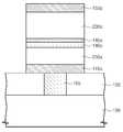
도 1은 본 발명의 실시예에 따른 자기 기억 소자를 나타내는 단면도이다.1 is a cross-sectional view showing a magnetic memory element according to an embodiment of the present invention.
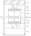
도 1을 참조하면, 기판(100) 상에 하부 층간 유전막(103)이 배치될 수 있다. 상기 기판(100)은 스위칭 요소(switching component, 미도시함)를 포함할 수 있다. 예컨대, 상기 스위칭 요소는 트랜지스터 또는 다이오드 등일 수 있다. 상기 하부 층간 유전막(103)은 상기 스위칭 요소 상에 배치될 수 있다. 상기 하부 층간 유전막(103)은 산화물, 질화물 및/또는 산화질화물 등을 포함할 수 있다. 하부 콘택 플러그(105)가 상기 하부 층간 유전막(103)을 관통할 수 있다. 상기 하부 콘택 플러그(105)는 상기 스위칭 요소의 일 단자(one terminal)에 전기적으로 접속될 수 있다. 예컨대, 상기 하부 콘택 플러그(105)는, 도펀트로 도핑된 반도체(ex, doped silicon 등), 금속(ex, 텅스텐 등), 도전성 금속 질화물 (ex, 질화 티타늄, 질화 탄탈늄 등), 금속-반도체 화합물(ex, 금속 실리사이드 등) 및 전이 금속(ex, 티타늄, 탄탈늄 등) 중에서 적어도 하나를 포함할 수 있다.Referring to FIG. 1, a lower interlayer
기준 자성 패턴(130a, reference magnetic pattern) 및 자유 자성 패턴(150a, free magnetic pattern)이 상기 하부 층간 유전막(103) 상에 배치될 수 있다. 터널 배리어 패턴(140b, tunnel barrier pattern)이 상기 기준 자성 패턴(130a) 및 자유 자성 패턴(150a) 사이에 개재될 수 있다. 상기 기준 자성 패턴(130a), 터널 배리어 패턴(140b) 및 자유 자성 패턴(150a)은 자기터널 접합 패턴(Magnetic tunnel junction pattern)에 포함될 수 있다. 일 실시예에 따르면, 도 1에 개시된 바와 같이, 상기 기준 자성 패턴(130a), 터널 배리어 패턴(140b) 및 자유 자성 패턴(150a)이 차례로 적층될 수 있다. 상기 기준 자성 패턴(130a)은 일 방향으로 고정된 자화 방향을 가질 수 있다. 상기 자유 자성 패턴(150a)은 상기 기준 자성 패턴(130a)의 고정된 자화 방향에 대하여 평행(parallel) 또는 반평행(anti-parallel)하게 변경 가능하도록 설정된다(configured). 상기 자유 자성 패턴(150a)은 상기 기준 자성 패턴(130a)의 측벽에 자기정렬된 측벽을 가질 수 있다.A reference
상기 터널 배리어 패턴(140b)은 중앙부(CP, central portion) 및 가장자리부(EP, edge portion)를 포함한다. 이때, 상기 터널 배리어 패턴(140b)의 가장자리부(EP)는 상기 터널 배리어 패턴(140b)의 중앙부(CP) 보다 두꺼운 것이 바람직하다. 일 실시예에 따르면, 상기 터널 배리어 패턴(140b)의 상기 중앙부(CP)는 실질적으로 균일한 두께를 가질 수 있다. 이와는 다르게, 상기 가장자리부(EP)의 외측벽으로부터 상기 중앙부(CP)를 향하여, 상기 가장자리부(EP)의 두께는 감소될 수 있다. 이때, 상기 가장자리부(EP)의 최소 두께는 상기 중앙부(CP)의 두께 보다 두껍다.The
일 실시예에 따르면, 상기 가장자리부(EP)의 상부면은 상기 중앙부(CP)의 상부면 보다 높은 레벨에 위치할 수 있다. 이때, 상기 가장자리부(EP)의 하부면은 상기 중앙부(CP)의 하부면과 실질적으로 공면(coplanar)을 이룰 수 있다.According to one embodiment, the upper surface of the edge portion EP may be located at a higher level than the upper surface of the central portion CP. At this time, the lower surface of the edge portion EP may be substantially coplanar with the lower surface of the central portion CP.
일 실시예에 따르면, 상기 터널 배리어 패턴(140b)의 중앙부(CP)의 두께(T1)는 스핀 확산 길이(spin diffusion distance) 보다 작을 수 있다. 상기 스핀 확산 길이는, 전자의 스핀 방향의 변경 없이 전자가 확산될 수 있는 길이를 의미할 수 있다. 예컨대, 상기 터널 배리어 패턴(140b)의 중앙부(CP)의 두께(T1)는 약 1 옹스트롬(angstrom) 내지 약 10 옹스트롬일 수 있다. 하지만, 본 발명은 여기에 한정되지 않는다.According to one embodiment, the thickness T1 of the central portion CP of the
상술된 바와 같이, 상기 터널 배리어 패턴(140b)의 가장자리부(EP)의 두께는 상기 중앙부(CP)의 두께 보다 두껍다. 일 실시예에 따르면, 상기 터널 배리어 패턴(140b)의 가장자리부(EP)의 두께는 상기 스핀 확산 길이 보다 클 수 있다. 상기 터널 배리어 패턴(140b)의 가장자리부(EP)의 최대 두께(T2)는 상기 터널 배리어 패턴(140b)의 중앙부(CP)의 두께(T1)의 약 5배와 같거나 작을 수 있다. 하지만, 본 발명은 여기에 한정되지 않는다.As described above, the thickness of the edge portion EP of the
상기 터널 배리어 패턴(140b)은 금속 산화물을 포함할 수 있다. 예컨대, 상기 터널 배리어 패턴(140b)은 산화마그네슘(magnesium oxide), 산화티타늄(titanium oxide), 산화알루미늄(aluminum oxide) 및 산화마그네슘아연(magnesium-zinc oxide) 중에서 적어도 하나를 포함할 수 있다.The
잔여 캐핑 패턴(145r, residual capping pattern)이 상기 터널 배리어 패턴(140b)의 중앙부(CP)와, 상기 자유 자성 패턴(150a) 사이에 개재될 수 있다. 상기 잔여 캐핑 패턴(145r)은 상기 터널 배리어 패턴(140b)의 중앙부(CP)의 상부면과 접촉될 수 있다. 일 실시예에 따르면, 상기 잔여 캐핑 패턴(145r)은 상기 자유 자성 패턴(150a)의 하부면과 접촉될 수도 있다. 상기 가장자리부(EP)의 상부면은 상기 잔여 캐핑 패턴(145r)의 상부면 보다 높은 레벨에 위치할 수 있다. 상기 터널 배리어 패턴(140b) 상에 배치된 상기 자유 자성 패턴(150a)의 하부면은 제1 부분 및 제2 부분을 포함할 수 있다. 상기 자유 자성 패턴(150a)의 하부면의 제1 부분은 상기 중앙부(CP) 상에 배치될 수 있으며, 상기 자유 자성 패턴(150a)의 하부면의 제2 부분은 상기 가장자리부(EP) 상에 배치될 수 있다. 이때, 상기 자유 자성 패턴(150a)의 하부면의 제2 부분은 상기 자유 자성 패턴(150a)의 하부면의 제1 부분 보다 높은 레벨에 위치할 수 있다.A
상기 잔여 캐핑 패턴(145r)은 금속으로 형성될 수 있다. 일 실시예에 따르면, 상기 잔여 캐핑 패턴(145r)의 금속 원소는 상기 터널 배리어 패턴(140b)의 금속 산화물 내 금속 원소와 동일할 수 있다. 예컨대, 상기 터널 배리어 패턴(140b)이 산화마그네슘을 포함하는 경우에, 상기 잔여 캐핑 패턴(145r)은 마그네슘으로 형성될 수 있다.The remaining
계속해서, 도 1을 참조하면, 상기 기준 자성 패턴(130a) 및 상기 자유 자성 패턴(150a)의 자화방향들은, 상기 터널 배리어 패턴(140a)의 하부면에 실질적으로 수평(horizontal)할 수 있다. 피닝 패턴(115a, pinning pattern)이 상기 기준 자성 패턴(130a)과 상기 하부 층간 유전막(103) 사이에 배치될 수 있다. 기준 보조 자성 패턴(120a)이 상기 피닝 패턴(115a)과 상기 기준 자성 패턴(130a) 사이에 개재될 수 있다. 교환 결합 패턴(125a, exchange couple pattern)이 상기 기준 보조 자성 패턴(120a) 및 상기 기준 자성 패턴(130a) 사이에 개재될 수 있다. 상기 피닝 패턴(115a), 기준 보조 자성 패턴(120a), 교환 결합 패턴(125a), 기준 자성 패턴(130a), 터널 배리어 패턴(140b), 잔여 캐핑 패턴(145r) 및 자유 자성 패턴(150a)이 상기 하부 층간 유전막(103) 상에 차례로 적층될 수 있다.Referring to FIG. 1, the magnetization directions of the reference
상기 피닝 패턴(115a)에 의하여, 상기 기준 자성 패턴(130a)의 자화방향이 상기 일 방향으로 고정될 수 있다. 예컨대, 상기 기준 보조 자성 패턴(120a)의 자화방향은 상기 피닝 패턴(115a)에 의하여 고정될 수 있다. 상기 기준 자성 패턴(120a)의 자화방향은 상기 교환 결합 패턴(125a)에 의하여 상기 기준 보조 자성 패턴(120a)의 지화방향과 반평행하게 고정될 수 있다. 상기 피닝 패턴(115a)은 반강자성체를 포함할 수 있다. 예컨대, 상기 피닝 패턴(115a)은 백금망간(PtMn), 이리듐망간(IrMn), 산화망간(MnO), 황화망간(MnS), 망간텔레륨(MnTe) 및 불화망간(MnF)에서 적어도 하나를 포함할 수 있다. 상기 교환 결합 패턴(125a)은 희유 금속(rare metal)을 포함할 수 있다. 예컨대, 상기 교환 결합 패턴(125a)은 루테늄(Ru), 이리듐(Ir) 및 로듐(Rh) 중에서 적어도 하나를 포함할 수 있다.The magnetization direction of the reference
상기 기준 자성 패턴(130a)은 강자성체를 포함할 수 있다. 예컨대, 상기 기준 자성 패턴(130a)은 코발트철붕소(CoFeB), 코발트철(CoFe), 니켈철(NiFe) 및 코발트철니켈(CoFeNi) 중에서 적어도 하나를 포함할 수 있다. 상기 자유 자성 패턴(150a)도 강자성체를 포함할 수 있다. 예컨대, 상기 자유 자성 패턴(150a)은 코발트철붕소(CoFeB), 코발트철(CoFe) 및 니켈철(NiFe), 코발트철니켈(CoFeNi) 중에서 적어도 하나를 포함할 수 있다. 이와 마찬가지로, 상기 기준 보조 자성 패턴(120a)도 강자성체를 포함할 수 있다. 예컨대, 상기 기준 보조 자성 패턴(120a)은 코발트철붕소(CoFeB), 코발트철(CoFe) 및 니켈철(NiFe), 코발트철니켈(CoFeNi) 중에서 적어도 하나를 포함할 수 있다. 일 실시예에 따르면, 상기 기준 자성 패턴(130a), 자유 자성 패턴(150a) 및 기준 보조 자성 패턴(120a)은 서로 동일한 강자성체를 포함하거나, 서로 다른 강자성체를 포함할 수 있다.The reference
일 실시예에 따르면, 상기 기준 보조 자성 패턴(120a) 및 교환 결합 패턴(125a)이 생략될 수 있다. 이 경우에, 상기 기준 자성 패턴(130a)은 상기 피닝 패턴(115a)과 직접 접촉될 수 있다.According to one embodiment, the reference auxiliary
제1 전극(110a)이 상기 피닝 패턴(115a) 및 하부 층간 유전막(103) 사이에 개재될 수 있다. 상기 제1 전극(110a)은 상기 하부 콘택 플러그(105)와 접속될 수 있다. 제2 전극(155a)이 상기 자유 자성 패턴(150a) 상에 배치될 수 있다. 상기 제1 및 제2 전극들(110a, 155a)은 도전 물질로 형성될 수 있다. 예컨대, 상기 제1 및 제2 전극들(110a, 155a)은 도전성 금속 질화물(ex, 질화 티타늄, 질화 탄탈늄 등)을 포함할 수 있다. 상기 제1 및 제2 전극들(110a, 155a)은 서로 동일한 도전 물질을 포함하거나, 서로 다른 도전 물질을 포함할 수 있다.The
상부 층간 유전막(160)이, 상기 제2 전극(155a)을 포함하는 상기 기판(100) 전면 상에 배치될 수 있다. 상부 콘택 플러그(165)가 상기 상부 층간 유전막(160)을 관통하여, 상기 제2 전극(155a)에 접속될 수 있다. 배선(170)이 상기 상부 층간 유전막(160) 상에 배치되어, 상기 상부 콘택 플러그(165)와 접속될 수 있다. 상기 배선(170)은 비트 라인에 해당할 수 있다.An
다음으로, 상술된 자기 기억 소자의 동작 방법을 설명한다. 상기 자유 자성 패턴(150a)의 자화방향은, 상기 자기터널 접합 패턴을 관통하는 프로그램 전류 내 전자들의 스핀 전송 토크(spin transfer torque)에 의하여 변경될 수 있다. 예컨대, 상기 자유 자성 패턴(150a)의 자화방향이 상기 기준 자성 패턴(130a)의 자화방향과 반평행한 경우에, 프로그램 전류는 상기 자유 자성 패턴(150a)으로부터 상기 기준 자성 패턴(130a)을 향하여 공급될 수 있다. 즉, 상기 프로그램 전류 내 전자들은 상기 기준 자성 패턴(130a)으로부터 상기 자유 자성 패턴(150a)을 향하여 공급될 수 있다. 상기 기준 자성 패턴(130a)을 통과한 전자들은 제1 전자들 및 제2 전자들을 포함할 수 있다. 상기 제1 전자들은 상기 기준 자성 패턴(130a)의 자화방향과 평행한 스핀들을 가질 수 있으며, 상기 제2 전자들은 상기 기준 자성 패턴(130a)의 자화방향과 반평행한 스핀들을 가질 수 있다. 상기 제1 전자들은 상기 자유 자성 패턴(150a) 내에 축적될 수 있다. 상기 자유 자성 패턴(150a) 내에 축적된 제1 전자들의 스핀 토크에 의하여, 상기 자유 자성 패턴(150a)의 자화방향이 상기 기준 자성 패턴(130a)의 자화방향과 평행하도록 변경될 수 있다.Next, a method of operating the above-described magnetic memory element will be described. The magnetization direction of the free
이와는 다르게, 상기 자유 자성 패턴(150a)의 자화방향이 상기 기준 자성 패턴(130a)의 자화방향과 평행할 수 있다. 이 경우에, 프로그램 전류는 상기 기준 자성 패턴(130a)으로부터 상기 자유 자성 패턴(150a)을 향하여 공급될 수 있다. 즉, 상기 프로그램 전류 내 전자들은 상기 자유 자성 패턴(150a)으로부터 상기 기준 자성 패턴(130a)을 향하여 공급될 수 있다. 상기 기준 자성 패턴(130a)의 자화방향과 평행한 스핀들을 갖는 제1 전자들은 상기 기준 자성 패턴(130a)을 통과할 수 있다. 상기 기준 자성 패턴(130a)의 자화방향과 반평행한 제2 전자들은, 상기 기준 자성 패턴(130a)의 자화방향에 기인하여 반사될 수 있다. 상기 반사된 제2 전자들은 상기 자유 자성 패턴(150a) 내에 축적될 수 있다. 상기 자유 자성 패턴(150a) 내에 축적된 제2 전자들의 스핀 토크에 의하여, 상기 자유 자성 패턴(150a)의 자화방향은 상기 기준 자성 패턴(130a)의 자화방향에 반평행 하게 변경될 수 있다.Alternatively, the magnetization direction of the free
상술된 자기 기억 소자에 따르면, 상기 터널 배리어 패턴(140b)의 가장자리부(EP)는 중앙부(CP) 보다 두껍다. 이에 따라, 상기 터널 배리어 패턴(140b)의 가장자리부(EP)를 통하여 흐르는 프로그램 전류 내 전자들 및/또는 판독 전류의 전자들의 량을 최소화시킬 수 있다. 그 결과, 우수한 신뢰성을 갖는 자기 기억 소자를 구현할 수 있다.According to the above-described magnetic memory element, the edge portion EP of the
패터닝 공정 등의 요인으로 인하여, 자기터널 접합 패턴의 가장자리 영역(edge domain)이 거칠어질 수 있다. 이에 따라, 자기터널 접합 패턴의 가장자리 영역을 통과하는 전자들의 스핀 방향들을 제어하는 것이 어려워질 수 있다. 예컨대, 상기 가장자리 영역을 통과하는 전자들의 스핀 방향들은 기준 및 자유 자성 패턴들의 자화방향들에 대하여 비평행(non parallel) 및 비반평행(non anti-parallel)할 수 있다. 이로 인하여, 자기터널 접합 패턴의 자기 저항비가 감소되거나, 요구되는 프로그램 전류량이 증가될 수 있다. 하지만, 상술된 바와 같이, 본 발명의 실시예에 따르면, 상기 터널 배리어 패턴(140b)의 가장자리부(EP)가 중앙부(CP) 보다 두꺼움으로써, 상기 터널 배리어 패턴(140b)의 가장자리부(EP)를 통과하는 전자들의 량을 최소화시킬 수 있다. 그 결과, 우수한 신뢰성을 갖는 자기 기억 소자를 구현할 수 있다.The edge domain of the magnetic tunnel junction pattern may be roughened due to factors such as the patterning process. Thus, it may be difficult to control the spin directions of electrons passing through the edge region of the magnetic tunnel junction pattern. For example, the spin directions of electrons passing through the edge region may be non-parallel and non-parallel to the magnetization directions of the reference and free magnetic patterns. As a result, the magnetoresistance ratio of the magnetic tunnel junction pattern can be reduced or the required amount of program current can be increased. However, as described above, according to the embodiment of the present invention, since the edge portion EP of the
또한, 프로그램 전류 내 전자들은 실질적으로 상기 터널 배리어 패턴(140b)의 중앙부(CP)를 통과할 수 있다. 이에 따라, 프로그램 전류 내 전자들의 터널링 면적이 감소되어, 프로그램 전류 내 전자 밀도가 증가될 수 있다. 그 결과, 프로그램 전류량을 감소시킬 수 있다. 이로써, 소비전력이 최소화되고 고집적화에 최적화된 자기 기억 소자를 구현할 수 있다.In addition, electrons in the program current can pass substantially through the central portion (CP) of the
다음으로, 실시예에 따른 자기 기억 소자의 변형예들을 설명한다. 변형예들에서 동일한 구성 요소들은 동일한 참조부호를 사용한다.Next, modified examples of the magnetic memory element according to the embodiment will be described. In the variations, the same components use the same reference numerals.
도 1에 개시된 자기 기억 소자에 따르면, 상기 기준 자성 패턴(130a)이 상기 터널 배리어 패턴(140b) 아래에 배치될 수 있으며, 상기 자유 자성 패턴(150a)이 상기 터널 배리어 패턴(140b) 위에 배치될 수 있다. 이와는 다르게, 상기 자유 자성 패턴(150a) 및 기준 자성 패턴(130a)이 각각 상기 터널 배리어 패턴(140b) 아래 및 위에 배치될 수도 있다. 이를 도면을 참조하여 설명한다.1, the reference
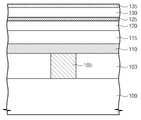
도 2는 본 발명의 실시예에 따른 자기 기억 소자의 일 변형예를 나타내는 단면도이다.2 is a cross-sectional view showing a modification of the magnetic memory element according to the embodiment of the present invention.
도 2를 참조하면, 변경 가능한 자화방향을 갖는 자유 자성 패턴(150a)이 터널 배리어 패턴(140b)의 하부면과, 제1 전극(110a)의 상부면 사이에 배치될 수 있다. 즉, 상기 자유 자성 패턴(150a)은 상기 터널 배리어 패턴(140b) 아래에 배치될 수 있다. 일 방향으로 고정된 자화방향을 갖는 기준 자성 패턴(130a)이 상기 터널 배리어 패턴(140b)의 상부면 상에 배치될 수 있다. 이 경우에, 잔여 캐핑 패턴(145r)은 상기 터널 배리어 패턴(140b)의 중앙부(CP)의 상부면과 상기 기준 자성 패턴(130a) 사이에 배치될 수 있다. 본 변형예에 따르면, 상기 잔여 캐핑 패턴(145r)은 상기 터널 배리어 패턴(140b)의 중앙부(CP)의 상부면, 및 상기 기준 자성 패턴(130a)의 하부면과 접촉될 수 있다.Referring to FIG. 2, a free
상기 터널 배리어 패턴(140b)의 가장자리부의 상부면은 상기 잔여 캐핑 패턴(145r)의 상부면 보다 높은 레벨에 위치할 수 있다. 상기 기준 자성 패턴(130a)의 하부면은, 제1 부분 및 제2 부분을 포함할 수 있다. 상기 기준 자성 패턴(130a)의 하부면의 제1 부분은 상기 잔여 캐핑 패턴(145r) 상에 배치될 수 있다. 상기 기준 자성 패턴(130a)의 하부면의 제2 부분은 상기 터널 배리어 패턴(140b)의 가장자리부(EP) 상에 배치될 수 있다. 이때, 상기 기준 자성 패턴(130a)의 하부면의 제2 부분은, 상기 기준 자성 패턴(130a)의 하부면의 제1 부분 보다 높은 레벨에 위치할 수 있다. 본 변형예에서도, 상기 터널 배리어 패턴(140b)의 중앙부(CP)의 하부면은 가장자리부(EP)의 하부면과 실질적으로 공면을 이룰 수 있다.The upper surface of the edge portion of the
상기 터널 배리어 패턴(140b) 상에 배치된 상기 자유 자성 패턴(150a)의 하부면은 제1 부분 및 제2 부분을 포함할 수 있다. 상기 자유 자성 패턴(150a)의 하부면의 제1 부분은 상기 중앙부(CP) 상에 배치될 수 있으며, 상기 자유 자성 패턴(150a)의 하부면의 제2 부분은 상기 가장자리부(EP) 상에 배치될 수 있다.The lower surface of the free
한편, 상술된 도 1 및 도 2의 기준 및 자유 자성 패턴들(130a, 150a)의 자화 방향들은, 상기 터널 배리어 패턴(140b)의 일면(예컨대, 중앙부(CP)의 하부면)에 대하여 실질적으로 수평(horizontal)할 수 있다. 하지만, 본 발명은 여기에 한정되지 않는다. 기준 및 자유 자성 패턴들의 자화 방향들은 터널 배리어 패턴의 일 면에 수직(perpendicular)할 수도 있다. 이를 도면들을 참조하여 설명한다.On the other hand, the magnetization directions of the reference and free
도 3은 본 발명의 실시예에 따른 자기 기억 소자의 다른 변형예를 나타내는 단면도이다.3 is a cross-sectional view showing another modification of the magnetic memory element according to the embodiment of the present invention.
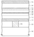
도 3을 참조하면, 기준 수직 자성 패턴(230a, reference perpendicular magnetic pattern), 터널 배리어 패턴(140b) 및 자유 수직 자성 패턴(250a, free perpendicular magnetic pattern)이 제1 전극(110a) 상에 차례로 적층될 수 있다. 제2 전극(155a)이 상기 자유 수직 자성 패턴(250a) 상에 배치될 수 있다.Referring to FIG. 3, a reference perpendicular
상기 기준 수직 자성 패턴(230a)은 일 방향으로 고정된 자화방향을 갖는다. 이때, 상기 기준 수직 자성 패턴(230a)의 고정된 자화방향은 상기 터널 배리어 패턴(140b)의 하부면에 실질적으로 수직(perpendicular)할 수 있다. 상기 자유 수직 자성 패턴(250a)의 자화 방향은, 상기 기준 수직 자성 패턴(230a)의 고정된 자화방향에 평행 또는 반평행 하게 변경 가능하도록 설정(configured)될 수 있다. 이에 따라, 상기 자유 수직 자성 패턴(250a)의 자화 방향도 상기 터널 배리어 패턴(140b)의 하부면에 실질적으로 수직할 수 있다.The reference perpendicular
상기 기준 수직 자성 패턴(230a)은 제1 임계 전류량을 가질 수 있으며, 상기 자유 수직 자성 패턴(250a)은 제2 임계 전류량을 가질 수 있다. 상기 제1 임계 전류량은 상기 기준 수직 자성 패턴(230a)의 자화 방향을 변경하는데 요구되는 전류량을 의미하고, 상기 제2 임계 전류량은 상기 자유 수직 자성 패턴(250a)의 자화 반향을 변경하는데 요구되는 전류량을 의미한다. 이때, 상기 기준 수직 자성 패턴(230a)의 제1 임계 전류량은, 상기 자유 수직 자성 패턴(250a)의 제2 임계 전류량 보다 크다. 이때, 프로그램 전류량은 상기 제1 임계 전류량 보다 작고 상기 제2 임계 전류량 보다 크다. 이로써, 상기 기준 수직 자성 패턴(230a)의 자화방향은 고정될 수 있으며, 상기 자유 수직 자성 패턴(230a)의 자화방향은 프로그램 동작에 의하여 변경 가능하다.The reference vertical
일 실시예에 따르면, 상기 기준 수직 자성 패턴(230a)이 상기 자유 수직 자성 패턴(250a) 보다 두꺼울 수 있다. 이로써, 상기 제1 임계 전류량이 상기 제2 임계 전류량 보다 클 수 있다. 일 실시예에 따르면, 상기 기준 수직 자성 패턴(230a)의 보자력이 상기 자유 수직 자성 패턴(230a)의 보자력 보다 클 수 있다. 이로써, 상기 제1 임계 전류량이 상기 제2 임계 전류량 보다 클 수 있다.According to one embodiment, the reference vertical
예컨대, 상기 기준 수직 자성 패턴(230a)은 수직 자성 물질(예컨대, CoFeTb, CoFeGd, L10 구조의 FePt, L10 구조의 FePd, L10 구조의 CoPd, L10 구조의 CoPt, 및/또는 조밀육방격자(Hexagonal Close Packed Lattice)를 갖는 CoPt 등), 및 수직 자성 구조체(예컨대, (Co/Pt)n, (CoFe/Pt)n, (CoFe/Pd)n, (Co/Pd)n, (Co/Ni)n, (CoNi/Pt)n, (CoCr/Pt)n 및/또는 (CoCr/Pd)n 등, n은 적층횟수) 중에서 적어도 하나를 포함할 수 있다. 상기 자유 수직 자성 패턴(250a)은 수직 자성 물질(예컨대, CoFeTb, CoFeGd, L10 구조의 FePt, L10 구조의 FePd, L10 구조의 CoPd, L10 구조의 CoPt, 및/또는 조밀육방격자(Hexagonal Close Packed Lattice)를 갖는 CoPt 등), 및 수직 자성 구조체(예컨대, (Co/Pt)m, (CoFe/Pt)m, (CoFe/Pd)m, (Co/Pd)m, (Co/Ni)m, (CoNi/Pt)m, (CoCr/Pt)m 및/또는 (CoCr/Pd)m 등, m은 적층횟수) 중에서 적어도 하나를 포함할 수 있다. 이때, 상기 기준 및 자유 수직 자성 패턴들(230a, 250a)은 상기 제1 임계 전류량 및 상기 제2 임계 전류량의 관계가 충족되도록 형성될 수 있다.For example, the reference perpendicular magnetic pattern (230a) is perpendicular to the magnetic material (for example, CoFeTb, CoFeGd, CoPt, and / or the dense hexagonal of CoPd, L10 structure of FePd, L10 structure of FePt, L10 structure of L10 structure (CoPt / Pd) n, (Co / Pd) n, (Co / Pt) n, (CoFe / Pt) n, / Ni) n, (CoNi / Pt) n, (CoCr / Pt) n and / or (CoCr / Pd) n and n is the number of stacking. The free vertical magnetic pattern (250a) is perpendicular to the magnetic material (for example, CoFeTb, CoPt, and / or the dense hexagonal lattice of CoFeGd, L10 structure of FePt, L10 structure of FePd, L10 structure of the CoPd, L10 structure ( (Co / Pt) m, (CoFe / Pd) m, (Co / Pd) m, (Co / Pt) m, ) m, (CoNi / Pt) m, (CoCr / Pt) m and / or (CoCr / Pd) m, and m is the number of lamination. At this time, the reference and free vertical
캐핑 잔여 패턴(145r)이 상기 터널 배리어 패턴(140b)의 중앙부(CP)의 상부면, 및 상기 자유 수직 자성 패턴(250a) 사이에 개재될 수 있다. 상기 캐핑 잔여 패턴(145r)은 상기 터널 배리어 패턴(140b)의 중앙부(CP)의 상부면, 및 상기 자유 수직 자성 패턴(250a)의 하부면과 접촉될 수 있다.The capping
도 4는 본 발명의 실시예에 따른 자기 기억 소자의 또 다른 변형예를 나타내는 단면도이다.4 is a cross-sectional view showing still another modification of the magnetic memory element according to the embodiment of the present invention.
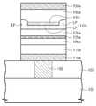
도 4를 참조하면, 제1 전극(110a) 상에 자유 수직 자성 패턴(250a), 터널 배리어 패턴(140b) 및 기준 수직 자성 패턴(230a)이 차례로 적층될 수 있다. 즉, 상기 자유 수직 자성 패턴(250a)이 상기 터널 배리어 패턴(140b) 아래에 위치할 수 있으며, 상기 기준 수직 자성 패턴(230a)이 상기 터널 배리어 패턴(140b) 위에 배치될 수 있다.Referring to FIG. 4, a free vertical
변 변형예에 따르면, 상기 잔여 캐핑 패턴(145r)은 상기 터널 배리어 패턴(140b)의 중앙부(CP)의 상부면, 및 상기 기준 수직 자성 패턴(230a) 사이에 배치될 수 있다. 상기 잔여 캐핑 패턴(145r)은 상기 터널 배리어 패턴(140b)의 중앙부(CP)의 상부면, 및 상기 기준 수직 자성 패턴(230a)의 하부면과 접촉될 수 있다.The
본 변형예에 따르면, 상기 제2 전극(155a)은 상기 기준 수직 자성 패턴(230a)의 상부면 상에 배치될 수 있다.According to this modification, the
다음으로, 본 발명의 실시예에 따른 자기 기억 소자의 제조 방법을 도면들을 참조하여 설명한다.Next, a method of manufacturing a magnetic memory element according to an embodiment of the present invention will be described with reference to the drawings.
도 5 내지 도 9는 본 발명의 실시예에 따른 자기 기억 소자의 제조 방법을 설명하기 위한 단면도들이다.5 to 9 are cross-sectional views illustrating a method of manufacturing a magnetic memory device according to an embodiment of the present invention.
도 5를 참조하면, 기판(100) 상에 하부 층간 유전막(103)을 형성할 수 있다. 상기 하부 층간 유전막(103)을 관통하는 하부 콘택 플러그(105)를 형성할 수 있다.Referring to FIG. 5, a lower
상기 하부 층간 유전막(103) 상에 제1 도전막(110), 피닝막(115), 기준 보조 자성막(120) 및 교환 결합막(125)을 차례로 형성할 수 있다. 상기 교환 결합막(125) 상에 기준 자성막(130)을 형성할 수 있다. 상기 제1 도전막(110)은 도전성 금속 질화막(ex, 티타늄 질화막 및/또는 탄탈늄 질화막 등)으로 형성될 수 있다. 상기 피닝막(115)은 반강자성체막(ex, 백금망간(PtMn)막, 이리듐망간(IrMn)막, 산화망간(MnO)막, 황화망간(MnS)막, 망간텔레륨(MnTe)막 및/또는 불화망간(MnF)막 등)으로 형성될 수 있다. 상기 기준 보조 자성막(120)은 강자성체막(ex, 코발트철붕소(CoFeB)막, 코발트철(CoFe)막, 니켈철(NiFe)막 및/또는 코발트철니켈(CoFeNi)막 등)으로 형성될 수 있다. 상기 교환 결합막(125)은 희유 금속막(ex, 루테늄(Ru)막, 이리듐(Ir)막 및/또는 로듐(Rh)막 등)으로 형성될 수 있다. 상기 기준 자성막(130)은 강자성체막(ex, 코발트철붕소(CoFeB)막, 코발트철(CoFe)막, 니켈철(NiFe)막 및/또는 코발트철니켈(CoFeNi)막 등)으로 형성될 수 있다.The first
상기 기준 자성막(130) 상에 기초-금속막(135)을 형성할 수 있다. 상기 기초-금속막(135)은 마그네슘(Mg), 알루미늄(Al), 티타늄(Ti) 및 마그네슘-아연(Mg-Zn) 중에 적어도 하나를 포함할 수 있다.The
도 6을 참조하면, 상기 기초-금속막(135)에 제1 산화 공정을 수행할 수 있다. 이에 따라, 상기 기초-금속막(135)이 산화되어, 기초-배리어막(140)이 형성될 수 있다. 상기 기초-배리어막(140)은 금속 산화막으로 형성될 수 있다. 예컨대, 상기 기초-배리어막(140)은 마그네슘 산화막, 알루미늄 산화막, 티타늄 산화막 및 마그네슘-아연 산화막 중에 적어도 하나를 포함할 수 있다. 일 실시예에 따르면, 상기 기초-금속막(135)은 상기 제1 산화 공정에 의하여 완전히 산화될 수 있다. 상기 제1 산화 공정은 열 산화 공정, 플라즈마 산화 공정 또는 열/플라즈마 산화 공정 등으로 수행할 수 있다.Referring to FIG. 6, a first oxidation process may be performed on the base-
이와는 달리, 상기 기초-배리어막(140)은 다른 방법으로 형성될 수도 있다. 일 실시예에 따르면, 상기 기초-배리어막(140)은 상기 기준 자성막(130) 상에 화학기상 증착 공정 및 원자층 증착 공정 중에서 적어도 하나에 의하여 형성될 수도 있다. 이 경우에도, 상기 기초-배리어막(140)은 금속 산화막(ex, 마그네슘 산화막, 알루미늄 산화막, 티타늄 산화막 및/또는 마그네슘-아연 산화막)으로 형성될 수 있다.Alternatively, the base-
상기 기초-배리어막(140)은 실질적으로 균일한 두께로 형성될 수 있다. 일 실시예에 따르면, 상기 기초-배리어막(140)은 약 1 옹스트롬 내지 약 10 옹스트롬의 두께로 형성될 수 있다. 하지만, 본 발명은 이 수치에 한정되지 않는다.The base-
도 7을 참조하면, 상기 기초-배리어막(140) 상에 캐핑막(145)을 형성할 수 있다. 상기 캐핑막(145)은 금속을 포함할 수 있다. 일 실시예에 따르면, 상기 캐핑막(145)의 금속은 상기 기초-배리어막(140) 내 금속과 동일한 금속을 포함할 수 있다. 예컨대, 상기 캐핑막(145)은 마그네슘(Mg), 알루미늄(Al), 티타늄(Ti) 및 마그네슘-아연(Mg-Zn) 중에 적어도 하나를 포함할 수 있다. 상기 캐핑막(145)은 상기 기초-배리어막(140) 바로 위(directly on)에 형성될 수 있다.Referring to FIG. 7, a
상기 캐핑막(145) 상에 자유 자성막(150) 및 제2 도전막(155)을 차례로 형성할 수 있다. 상기 자유 자성막(150)은 강자성체막(ex, 코발트철붕소(CoFeB)막, 코발트철(CoFe)막, 니켈철(NiFe)막 및/또는 코발트철니켈(CoFeNi)막 등)으로 형성될 수 있다. 상기 제2 도전막(155)은 도전성 금속 질화막(ex, 티타늄 질화막, 탄탈늄 질화막 등)으로 형성될 수 있다.A free
도 8 및 도 9를 참조하면, 상기 제2 도전막(155), 자유 자성막(150), 캐핑막(145), 기초-배리어막(140), 기준 자성막(130), 교환 결합막(125), 기준 보조 자성막(120), 피닝막(115) 및 제1 도전막(110)을 연속적으로 패터닝할 수 있다. 이로 인하여, 상기 하부 층간 유전막(103) 상에 차례로 적층된 제1 전극(110a), 피닝 패턴(115a), 기준 보조 자성 패턴(120a), 교환 결합 패턴(125a), 기준 자성 패턴(130a), 기초-배리어 패턴(140a), 캐핑 패턴(145a), 자유 자성 패턴(150a) 및 제2 전극(155a)이 차례로 형성될 수 있다. 상기 패턴들(110a, 115a, 120a, 125a, 130a, 140a, 145a, 150a, 155a)의 측벽들은 서로 자기 정렬될 수 있다.8 and 9, the second
상기 캐핑 패턴(145a)에 제2 산화 공정을 수행할 수 있다. 이에 따라, 상기 캐핑 패턴(145a)의 노출된 측벽을 통하여, 상기 캐핑 패턴(145a)의 가장자리부가 산화된다. 이에 따라, 터널 배리어 패턴(140b)이 형성된다. 이때, 상기 캐핑 패턴(145a)의 중앙부는 산화되지 않는 것이 바람직하다. 이에 따라, 상기 제2 산화 공정을 수행한 후에, 잔여 캐핑 패턴(145r)이 형성될 수 있다. 상기 제2 산화 공정은 열 산화 공정, 플라즈마 산화 공정 또는 열/플라즈마 산화 공정 등으로 수행할 수 있다.A second oxidation process may be performed on the
상기 터널 배리어 패턴(140b)은 상기 기초-배리어 패턴(140a) 및 상기 캐핑 패턴(145a)의 산화된 가장자리부를 포함한다. 이로써, 상기 터널 배리어 패턴(140b)는 중앙부(CP) 및 상기 중앙부(CP) 보다 두꺼운 가장자리부(EP)를 포함한다. 상기 잔여 캐핑 패턴(145r)은 상기 터널 배리어 패턴(140b)의 중앙부(CP) 상에 형성된다. 상기 터널 배리어 패턴(140b)의 중앙부(CP)는 상기 기초-배리어막(140a)의 중앙부에 해당할 수 있으며, 상기 터널 배리어 패턴(140b)의 가장자리부(EP)는, 상기 기초-배리어막(140a)의 가장자리부 및 상기 캐핑 패턴(145a)의 산화된 가장자리부를 포함할 수 있다. 상기 캐핑 패턴(145a)은 상기 기초-배리어막(140a) 내 금속과 동일한 금속을 포함함으로써, 상기 캐핑 패턴(145a)의 산화된 가장자리부는 상기 기초-배리어막(140a)과 동일한 금속 산화물을 포함할 수 있다.The
일 실시예에 따르면, 상기 제2 산화 공정에 의하여 상기 터널 배리어 패턴(140b)의 가장자리부(EP)가 형성됨으로써, 상기 터널 배리어 패턴(140b)의 가장자리부(EP)의 상부면은 상기 잔여 캐핑 패턴(145r)의 상부면 보다 높은 레벨에 위치할 수 있다.The edge portion EP of the
이어서, 도 1의 상부 층간 유전막(160), 상부 콘택 플러그(165) 및 배선(170)을 차례로 형성할 수 있다.Then, the
상술된 자기 기억 소자의 제조 방법에 따르면, 상기 기초-배리어막(140) 상에 상기 캐핑막(145)을 형성하고, 이들(145, 140)을 패터닝하여, 기초-배리어 패턴(140a) 및 캐핑 패턴(145a)을 형성할 수 있다. 이어서 캐핑 패턴(145a)의 가장자리부를 산화시켜, 상기 터널 배리어 패턴(140b)을 형성할 수 있다. 이때, 상기 캐핑 패턴(145a)의 중앙부는 산화되지 않아서, 잔여 캐핑 패턴(145r)이 형성된다. 이로 인하여, 중앙부(CP) 보다 두꺼운 가장자리부(EP)를 갖는 상기 터널 배리어 패턴(140b)을 구현할 수 있다.According to the above-described method for manufacturing a magnetic memory element, the
다음으로, 도 2에 개시된 자기 기억 소자의 제조 방법을 도면들을 참조하여 설명한다.Next, a method of manufacturing the magnetic memory element shown in Fig. 2 will be described with reference to the drawings.
도 10 내지 도 12는 본 발명의 실시예에 따른 자기 기억 소자의 제조 방법의 일 변형예를 설명하기 위한 단면도들이다.10 to 12 are cross-sectional views for explaining a modification of the method of manufacturing a magnetic memory device according to an embodiment of the present invention.
도 10을 참조하면, 하부 층간 유전막(103) 상에 제1 도전막(110), 자유 자성막(150) 및 기초-배리어막(140)을 차례로 형성할 수 있다. 도 5 및 도 6을 참조하여 설명한 바와 같이, 상기 기초-배리어막(140)은 기초-도전막(135)의 형성 공정 및 제1 산화 공정을 차례로 수행하여 형성되거나, 화학기상 증착 공정 및/또는 원자층 증착 공정으로 형성될 수 있다.10, the first
상기 기초-배리어막(140) 상에 캐핑막(145)을 형성할 수 있다. 상기 캐핑막(145) 상에 기준 자성막(130), 교환 결합막(125), 기준 보조 자성막(120), 피닝막(115) 및 제2 도전막(155)을 차례로 형성할 수 있다.The
도 11을 참조하면, 상기 제2 도전막(155), 피닝막(115), 기준 보조 자성막(120), 교환 결합막(125), 기준 자성막(130), 캐핑막(145), 기초-배리어막(140), 자유 자성막(150) 및 제1 도전막(110)을 연속적으로 패터닝할 수 있다. 이로써, 상기 하부 층간 유전막(103) 상에 차례로 적층된, 제1 전극(110a), 자유 자성 패턴(150), 기초-배리어 패턴(140a), 캐핑 패턴(145a), 기준 자성 패턴(130a), 교환 결합 패턴(125a), 기준 보조 자성 패턴(120a), 피닝 패턴(115a) 및 제2 전극(155a)이 차례로 형성될 수 있다.Referring to FIG. 11, the second
도 12를 참조하면, 상기 캐핑 패턴(145a)의 가장자리부를 산화시키어, 터널 배리어 패턴(140b)을 형성할 수 있다. 이때, 상기 캐핑 패턴(145a)의 중앙부는 산화되지 않는다. 이로써, 잔여 캐핑 패턴(145r)이 상기 터널 배리어 패턴(140b)의 중앙부(CP)의 상부면 및 기준 자성 패턴(130a)의 하부면 사이에 형성될 수 있다. 상기 잔여 캐핑 패턴(145r)은 상기 캐핑 패턴(145a)의 산화되지 않은 중앙부에 해당한다. 이어서, 도 2의 상부 층간 유전막(160), 상부 콘택 플러그(165) 및 배선(170)을 차례로 형성할 수 있다.Referring to FIG. 12, the edge portion of the
다음으로, 도 3에 개시된 자기 기억 소자의 제조 방법을 설명한다.Next, the manufacturing method of the magnetic memory element shown in Fig. 3 will be described.
도 13 및 도 14는 본 발명의 실시예에 따른 자기 기억 소자의 제조 방법의 다른 변형예를 설명하기 위한 단면도들이다.13 and 14 are cross-sectional views for explaining another modification of the manufacturing method of the magnetic memory device according to the embodiment of the present invention.
도 13을 참조하면, 하부 층간 유전막(103) 상에 제1 도전막, 기준 수직 자성막, 기초-배리어막, 캐핑막, 자유 수직 자성막 및 제2 도전막을 차례로 형성할 수 있다. 상기 기준 수직 자성막은 상기 자유 수직 자성막 보다 두껍게 형성될 수 있다. 및/또는 상기 기준 수직 자성막의 보자력이 상기 자유 수직 자성막의 보자력 보다 클 수 있다. 상기 기준 수직 자성막은 수직 자성 물질 및 수직 자성 구조체 중에서 적어도 하나를 포함할 수 있다. 상기 자유 수직 자성막은 수직 자성 물질 및 수직 자성 구조체 중에서 적어도 하나를 포함할 수 있다.Referring to FIG. 13, a first conductive film, a reference vertical magnetic film, a base-barrier film, a capping film, a free vertical magnetic film, and a second conductive film may be sequentially formed on the lower
상기 제2 도전막, 자유 수직 자성막, 캐핑막, 기초-배리어막, 기준 수직 자성막 및 제1 도전막을 연속적으로 패터닝할 수 있다. 이로써, 차례로 적층된 제1 전극(110a), 기준 수직 자성 패턴(230a), 기초-배리어 패턴(140a), 캐핑 패턴(145a), 자유 수직 자성 패턴(250a) 및 제2 전극(155a)이 상기 하부 층간 유전막(103) 상에 형성될 수 있다. The second conductive layer, the free vertical magnetic layer, the capping layer, the base-barrier layer, the reference vertical magnetic layer, and the first conductive layer may be patterned successively. Thus, the
도 14를 참조하면, 이어서, 상기 캐핑 패턴(145a)의 가장자리부를 산화시키어, 터널 배리어 패턴(140b)을 형성할 수 있다. 이때, 상기 캐핑 패턴(145a)의 중앙부는 산화되지 않는다. 이로써, 잔여 캐핑 패턴(145r)이 상기 터널 배리어 패턴(140b)의 중앙부(CP)의 상부면 및 자유 수직 자성 패턴(250a)의 하부면 사이에 형성될 수 있다. 이어서, 도 3의 상부 층간 유전막(160), 상부 콘택 플러그(165) 및 배선(170)을 차례로 형성할 수 있다.Referring to FIG. 14, the edge portion of the
다음으로, 도 4에 개시된 자기 기억 소자의 제조 방법을 설명한다.Next, a manufacturing method of the magnetic memory element shown in Fig. 4 will be described.
도 15 및 도 16은 본 발명의 실시예에 따른 자기 기억 소자의 제조 방법의 또 다른 변형예를 설명하기 위한 단면도들이다.15 and 16 are cross-sectional views for explaining still another modification of the method for manufacturing a magnetic memory device according to the embodiment of the present invention.
도 15를 참조하면, 하부 층간 유전막(103) 상에 제1 도전막, 자유 수직 자성막, 기초-배리어막, 캐핑막, 기준 수직 자성막 및 제2 도전막을 차례로 형성할 수 있다. 상기 제2 도전막, 기준 수직 자성막, 캐핑막, 기초-배리어막, 자유 수직 자성막 및 제1 도전막을 연속적으로 패터닝할 수 있다. 이로써, 차례로 적층된 제1 전극(110a), 자유 수직 자성 패턴(250a), 기초-배리어 패턴(140a), 캐핑 패턴(145a), 기준 수직 자성 패턴(230a) 및 제2 전극(155a)이 상기 하부 층간 유전막(103) 상에 형성될 수 있다.Referring to FIG. 15, a first conductive layer, a free vertical magnetic layer, a base-barrier layer, a capping layer, a reference vertical magnetic layer, and a second conductive layer may be sequentially formed on the lower
도 16을 참조하면, 이어서, 상기 캐핑 패턴(145a)의 가장자리부를 산화시키어, 터널 배리어 패턴(140b)을 형성할 수 있다. 이때, 상기 캐핑 패턴(145a)의 중앙부는 산화되지 않는다. 이로써, 잔여 캐핑 패턴(145r)이 상기 터널 배리어 패턴(140b)의 중앙부(CP)의 상부면 및 기준 수직 자성 패턴(230a)의 하부면 사이에 형성될 수 있다. 이어서, 도 3의 상부 층간 유전막(160), 상부 콘택 플러그(165) 및 배선(170)을 차례로 형성할 수 있다.Referring to FIG. 16, the edge portion of the
상술된 실시예들에서 개시된 자기 기억 소자들은 다양한 형태들의 반도체 패키지(semiconductor package)로 구현될 수 있다. 예를 들면, 본 발명의 실시예들에 따른 자기 기억 소자들은 PoP(Package on Package), Ball grid arrays(BGAs), Chip scale packages(CSPs), Plastic Leaded Chip Carrier(PLCC), Plastic Dual In-Line Package(PDIP), Die in Waffle Pack, Die in Wafer Form, Chip On Board(COB), Ceramic Dual In-Line Package(CERDIP), Plastic Metric Quad Flat Pack(MQFP), Thin Quad Flatpack(TQFP), Small Outline(SOIC), Shrink Small Outline Package(SSOP), Thin Small Outline(TSOP), Thin Quad Flatpack(TQFP), System In Package(SIP), Multi Chip Package(MCP), Wafer-level Fabricated Package(WFP), Wafer-Level Processed Stack Package(WSP) 등의 방식으로 패키징될 수 있다.The magnetic storage elements disclosed in the above embodiments can be implemented in various types of semiconductor packages. For example, the magnetic storage elements according to embodiments of the present invention may be implemented as a package on package (PoP), ball grid arrays (BGAs), chip scale packages (CSPs), plastic leaded chip carriers Die in Wafer Form, Chip On Board (COB), Ceramic Dual In-Line Package (CERDIP), Plastic Metric Quad Flat Pack (MQFP), Thin Quad Flatpack (TQFP), Small Outline (SOIC), Shrink Small Outline Package (SSOP), Thin Small Outline (TSOP), Thin Quad Flatpack (TQFP), System In Package (SIP), Multi Chip Package (MCP), Wafer-level Fabricated Package -Level Processed Stack Package (WSP) or the like.
본 발명의 실시예들에 따른 자기 기억 소자가 실장된 패키지는 상기 자기 기억 소자를 제어하는 컨트롤러 및/또는 논리 소자 등을 더 포함할 수도 있다.The package on which the magnetic storage element according to the embodiments of the present invention is mounted may further include a controller and / or a logic element for controlling the magnetic storage element.
이상, 첨부된 도면들을 참조하여 본 발명의 실시예들을 설명하였지만, 본 발명은 그 기술적 사상이나 필수적인 특징을 변경하지 않고서 다른 구체적인 형태로 실시될 수도 있다. 그러므로 이상에서 기술한 실시예들에는 모든 면에서 예시적인 것이며 한정적이 아닌 것으로 이해해야만 한다.Although the embodiments of the present invention have been described with reference to the accompanying drawings, the present invention may be embodied in other specific forms without departing from the spirit or essential characteristics thereof. It is therefore to be understood that the above-described embodiments are illustrative and non-restrictive in every respect.
Claims (10)
Translated fromKorean상기 제1 자성 패턴 및 제2 자성 패턴 사이에 개재된 터널 배리어 패턴; 및
상기 터널 배리어 패턴의 중앙부와 상기 제2 자성 패턴 사이의 잔여 캐핑 패턴을 포함하되,
상기 터널 배리어 패턴의 가장자리부는 상기 터널 배리어 패턴의 상기 중앙부 보다 두껍고, 상기 터널 배리어 패턴의 상기 중앙부는 균일한 두께를 가지고,
상기 제2 자성 패턴의 하면은 상기 잔여 캐핑 패턴의 상면 및 상기 터널 배리어 패턴의 상기 가장자리부의 상면과 접하는 자기 기억 소자.A first magnetic pattern and a second magnetic pattern disposed on a substrate;
A tunnel barrier pattern interposed between the first magnetic pattern and the second magnetic pattern; And
And a residual capping pattern between a central portion of the tunnel barrier pattern and the second magnetic pattern,
The edge portion of the tunnel barrier pattern is thicker than the central portion of the tunnel barrier pattern, the central portion of the tunnel barrier pattern has a uniform thickness,
And the lower surface of the second magnetic pattern is in contact with the upper surface of the remaining capping pattern and the upper surface of the edge portion of the tunnel barrier pattern.
상기 잔여 캐핑 패턴은 금속으로 형성되고,
상기 터널 배리어 패턴은 금속 산화물을 포함하는 자기 기억 소자.The method according to claim 1,
The remaining capping pattern is formed of a metal,
Wherein the tunnel barrier pattern comprises a metal oxide.
상기 터널 배리어 패턴 내 금속 산화물은, 상기 잔여 캐핑 패턴과 동일한 금속을 포함하는 자기 기억 소자.The method of claim 3,
Wherein the metal oxide in the tunnel barrier pattern comprises the same metal as the remaining capping pattern.
상기 제1 자성 패턴, 상기 터널 배리어 패턴, 및 상기 제2 자성 패턴은 상기 기판 상에 차례로 적층되고,
상기 터널 배리어 패턴의 상기 가장자리부의 상기 상면은, 상기 터널 배리어 패턴의 상기 중앙부의 상기 상면 보다 높은 레벨에 위치하고,
상기 터널 배리어 패턴의 상기 가장자리부의 하면은 상기 터널 배리어 패턴의 상기 중앙부의 하면과 공면(coplanar)을 이루는 자기 기억 소자.The method according to claim 1,
Wherein the first magnetic pattern, the tunnel barrier pattern, and the second magnetic pattern are sequentially stacked on the substrate,
The upper surface of the edge portion of the tunnel barrier pattern is located at a higher level than the upper surface of the central portion of the tunnel barrier pattern,
And a bottom surface of said edge portion of said tunnel barrier pattern coplanar with a bottom surface of said central portion of said tunnel barrier pattern.
상기 터널 배리어 패턴의 상기 가장자리부의 최대 두께는, 상기 터널 배리어 패턴의 상기 중앙부의 두께의 5배와 같거나 작은 자기 기억 소자.The method according to claim 1,
Wherein the maximum thickness of the edge portion of the tunnel barrier pattern is equal to or less than five times the thickness of the center portion of the tunnel barrier pattern.
상기 제1 및 제2 자성 패턴들 중에서 어느 하나는, 일 방향으로 고정된 자화 방향을 갖고,
상기 제1 및 제2 자성 패턴들 중에서 다른 하나는, 상기 고정된 자화 방향에 대하여 평행 또는 반평행하게 변경 가능하도록 설정된 자기 기억 소자.The method according to claim 1,
Wherein one of the first and second magnetic patterns has a magnetization direction fixed in one direction,
And the other of the first and second magnetic patterns is changeable in parallel or antiparallel with respect to the fixed magnetization direction.
상기 제1 자성막 상에 기초 배리어막을 형성하는 것;
상기 기초 배리어막 상에 캐핑막 및 제2 자성막을 차례로 형성하는 것;
상기 제2 자성막, 캐핑막, 기초 배리어막 및 제1 자성막을 연속적으로 패터닝하여, 차례로 적층된 제1 자성 패턴, 기초 배리어 패턴, 캐핑 패턴 및 제2 자성 패턴을 형성하는 것; 및
상기 캐핑 패턴의 가장자리부를 산화시켜, 터널 배리어 패턴을 형성하는 것을 포함하되,
상기 제2 자성 패턴은 상기 캐핑 패턴의 중앙부의 상면, 및 상기 캐핑 패턴의 산화된 가장자리부의 상면과 접하는 자기 기억 소자의 제조 방법.Forming a first magnetic film on the substrate;
Forming a base barrier film on the first magnetic film;
Forming a capping layer and a second magnetic layer in this order on the base barrier layer;
Continuously patterning the second magnetic film, the capping film, the base barrier film, and the first magnetic film to form a first magnetic pattern, a base barrier pattern, a capping pattern, and a second magnetic pattern sequentially stacked; And
Oxidizing the edge portion of the capping pattern to form a tunnel barrier pattern,
Wherein the second magnetic pattern is in contact with the upper surface of the central portion of the capping pattern and the upper surface of the oxidized edge portion of the capping pattern.
상기 캐핑 패턴의 상기 가장자리부 옆에 위치한 상기 캐핑 패턴의 상기 중앙부는 산화되지 않고,
상기 터널 배리어 패턴은 상기 기초 배리어 패턴 및 상기 캐핑 패턴의 상기 산화된 가장자리부를 포함하는 자기 기억 소자의 제조 방법.The method of claim 8,
The central portion of the capping pattern located beside the edge portion of the capping pattern is not oxidized,
Wherein the tunnel barrier pattern includes the base barrier pattern and the oxidized edge portions of the capping pattern.
상기 터널 배리어 패턴의 가장자리부는 상기 터널 배리어 패턴의 중앙부 보다 두껍고, 상기 터널 배리어 패턴의 중앙부는 균일한 두께를 갖는 자기 기억 소자의 제조 방법.The method of claim 9,
Wherein an edge portion of the tunnel barrier pattern is thicker than a center portion of the tunnel barrier pattern and a central portion of the tunnel barrier pattern has a uniform thickness.
Priority Applications (2)
| Application Number | Priority Date | Filing Date | Title |
|---|---|---|---|
| KR1020110048963AKR101811315B1 (en) | 2011-05-24 | 2011-05-24 | Magnetic memory devices and methods of fabricating the same |
| US13/479,337US8853807B2 (en) | 2011-05-24 | 2012-05-24 | Magnetic devices and methods of fabricating the same |
Applications Claiming Priority (1)
| Application Number | Priority Date | Filing Date | Title |
|---|---|---|---|
| KR1020110048963AKR101811315B1 (en) | 2011-05-24 | 2011-05-24 | Magnetic memory devices and methods of fabricating the same |
Publications (2)
| Publication Number | Publication Date |
|---|---|
| KR20120130903A KR20120130903A (en) | 2012-12-04 |
| KR101811315B1true KR101811315B1 (en) | 2017-12-27 |
Family
ID=47218679
Family Applications (1)
| Application Number | Title | Priority Date | Filing Date |
|---|---|---|---|
| KR1020110048963AActiveKR101811315B1 (en) | 2011-05-24 | 2011-05-24 | Magnetic memory devices and methods of fabricating the same |
Country Status (2)
| Country | Link |
|---|---|
| US (1) | US8853807B2 (en) |
| KR (1) | KR101811315B1 (en) |
Families Citing this family (84)
| Publication number | Priority date | Publication date | Assignee | Title |
|---|---|---|---|---|
| US9064589B2 (en)* | 2011-11-09 | 2015-06-23 | Qualcomm Incorporated | Three port MTJ structure and integration |
| JP2013232497A (en)* | 2012-04-27 | 2013-11-14 | Renesas Electronics Corp | Magnetic material device and manufacturing method thereof |
| KR20140112628A (en)* | 2013-03-12 | 2014-09-24 | 에스케이하이닉스 주식회사 | Semiconductor device and method for manufacturing the same, and micro processor, processor, system, data storage system and memory system including the semiconductor device |
| CN108320769A (en) | 2013-03-15 | 2018-07-24 | 英特尔公司 | Include the logic chip of inserted magnetic tunnel knot |
| KR102105078B1 (en) | 2013-05-30 | 2020-04-27 | 삼성전자주식회사 | Magnetic memory devices |
| US20150279904A1 (en)* | 2014-04-01 | 2015-10-01 | Spin Transfer Technologies, Inc. | Magnetic tunnel junction for mram device |
| US9263667B1 (en)* | 2014-07-25 | 2016-02-16 | Spin Transfer Technologies, Inc. | Method for manufacturing MTJ memory device |
| US9337412B2 (en) | 2014-09-22 | 2016-05-10 | Spin Transfer Technologies, Inc. | Magnetic tunnel junction structure for MRAM device |
| US9728712B2 (en) | 2015-04-21 | 2017-08-08 | Spin Transfer Technologies, Inc. | Spin transfer torque structure for MRAM devices having a spin current injection capping layer |
| US10468590B2 (en) | 2015-04-21 | 2019-11-05 | Spin Memory, Inc. | High annealing temperature perpendicular magnetic anisotropy structure for magnetic random access memory |
| US9853206B2 (en) | 2015-06-16 | 2017-12-26 | Spin Transfer Technologies, Inc. | Precessional spin current structure for MRAM |
| US9773974B2 (en) | 2015-07-30 | 2017-09-26 | Spin Transfer Technologies, Inc. | Polishing stop layer(s) for processing arrays of semiconductor elements |
| US10163479B2 (en) | 2015-08-14 | 2018-12-25 | Spin Transfer Technologies, Inc. | Method and apparatus for bipolar memory write-verify |
| US9705071B2 (en)* | 2015-11-24 | 2017-07-11 | International Business Machines Corporation | Structure and method to reduce shorting and process degradation in STT-MRAM devices |
| US9515252B1 (en)* | 2015-12-29 | 2016-12-06 | International Business Machines Corporation | Low degradation MRAM encapsulation process using silicon-rich silicon nitride film |
| US9741926B1 (en) | 2016-01-28 | 2017-08-22 | Spin Transfer Technologies, Inc. | Memory cell having magnetic tunnel junction and thermal stability enhancement layer |
| US10991410B2 (en) | 2016-09-27 | 2021-04-27 | Spin Memory, Inc. | Bi-polar write scheme |
| US10628316B2 (en) | 2016-09-27 | 2020-04-21 | Spin Memory, Inc. | Memory device with a plurality of memory banks where each memory bank is associated with a corresponding memory instruction pipeline and a dynamic redundancy register |
| US11119910B2 (en) | 2016-09-27 | 2021-09-14 | Spin Memory, Inc. | Heuristics for selecting subsegments for entry in and entry out operations in an error cache system with coarse and fine grain segments |
| US10437491B2 (en) | 2016-09-27 | 2019-10-08 | Spin Memory, Inc. | Method of processing incomplete memory operations in a memory device during a power up sequence and a power down sequence using a dynamic redundancy register |
| US10460781B2 (en) | 2016-09-27 | 2019-10-29 | Spin Memory, Inc. | Memory device with a dual Y-multiplexer structure for performing two simultaneous operations on the same row of a memory bank |
| US10366774B2 (en) | 2016-09-27 | 2019-07-30 | Spin Memory, Inc. | Device with dynamic redundancy registers |
| US11119936B2 (en) | 2016-09-27 | 2021-09-14 | Spin Memory, Inc. | Error cache system with coarse and fine segments for power optimization |
| US10360964B2 (en) | 2016-09-27 | 2019-07-23 | Spin Memory, Inc. | Method of writing contents in memory during a power up sequence using a dynamic redundancy register in a memory device |
| US10818331B2 (en) | 2016-09-27 | 2020-10-27 | Spin Memory, Inc. | Multi-chip module for MRAM devices with levels of dynamic redundancy registers |
| US10446210B2 (en) | 2016-09-27 | 2019-10-15 | Spin Memory, Inc. | Memory instruction pipeline with a pre-read stage for a write operation for reducing power consumption in a memory device that uses dynamic redundancy registers |
| US11151042B2 (en) | 2016-09-27 | 2021-10-19 | Integrated Silicon Solution, (Cayman) Inc. | Error cache segmentation for power reduction |
| US10546625B2 (en) | 2016-09-27 | 2020-01-28 | Spin Memory, Inc. | Method of optimizing write voltage based on error buffer occupancy |
| US10437723B2 (en) | 2016-09-27 | 2019-10-08 | Spin Memory, Inc. | Method of flushing the contents of a dynamic redundancy register to a secure storage area during a power down in a memory device |
| KR102615694B1 (en)* | 2016-11-02 | 2023-12-21 | 삼성전자주식회사 | Data storage devices and a method for manufacturing the same |
| US10665777B2 (en) | 2017-02-28 | 2020-05-26 | Spin Memory, Inc. | Precessional spin current structure with non-magnetic insertion layer for MRAM |
| US10672976B2 (en) | 2017-02-28 | 2020-06-02 | Spin Memory, Inc. | Precessional spin current structure with high in-plane magnetization for MRAM |
| US10032978B1 (en) | 2017-06-27 | 2018-07-24 | Spin Transfer Technologies, Inc. | MRAM with reduced stray magnetic fields |
| US10656994B2 (en) | 2017-10-24 | 2020-05-19 | Spin Memory, Inc. | Over-voltage write operation of tunnel magnet-resistance (“TMR”) memory device and correcting failure bits therefrom by using on-the-fly bit failure detection and bit redundancy remapping techniques |
| US10481976B2 (en) | 2017-10-24 | 2019-11-19 | Spin Memory, Inc. | Forcing bits as bad to widen the window between the distributions of acceptable high and low resistive bits thereby lowering the margin and increasing the speed of the sense amplifiers |
| US10529439B2 (en) | 2017-10-24 | 2020-01-07 | Spin Memory, Inc. | On-the-fly bit failure detection and bit redundancy remapping techniques to correct for fixed bit defects |
| US10489245B2 (en) | 2017-10-24 | 2019-11-26 | Spin Memory, Inc. | Forcing stuck bits, waterfall bits, shunt bits and low TMR bits to short during testing and using on-the-fly bit failure detection and bit redundancy remapping techniques to correct them |
| US10679685B2 (en) | 2017-12-27 | 2020-06-09 | Spin Memory, Inc. | Shared bit line array architecture for magnetoresistive memory |
| US10395711B2 (en) | 2017-12-28 | 2019-08-27 | Spin Memory, Inc. | Perpendicular source and bit lines for an MRAM array |
| US10516094B2 (en) | 2017-12-28 | 2019-12-24 | Spin Memory, Inc. | Process for creating dense pillars using multiple exposures for MRAM fabrication |
| US10360962B1 (en) | 2017-12-28 | 2019-07-23 | Spin Memory, Inc. | Memory array with individually trimmable sense amplifiers |
| US10395712B2 (en) | 2017-12-28 | 2019-08-27 | Spin Memory, Inc. | Memory array with horizontal source line and sacrificial bitline per virtual source |
| US10424726B2 (en) | 2017-12-28 | 2019-09-24 | Spin Memory, Inc. | Process for improving photoresist pillar adhesion during MRAM fabrication |
| US10811594B2 (en) | 2017-12-28 | 2020-10-20 | Spin Memory, Inc. | Process for hard mask development for MRAM pillar formation using photolithography |
| US10891997B2 (en) | 2017-12-28 | 2021-01-12 | Spin Memory, Inc. | Memory array with horizontal source line and a virtual source line |
| US10367139B2 (en) | 2017-12-29 | 2019-07-30 | Spin Memory, Inc. | Methods of manufacturing magnetic tunnel junction devices |
| US10840436B2 (en) | 2017-12-29 | 2020-11-17 | Spin Memory, Inc. | Perpendicular magnetic anisotropy interface tunnel junction devices and methods of manufacture |
| US10840439B2 (en) | 2017-12-29 | 2020-11-17 | Spin Memory, Inc. | Magnetic tunnel junction (MTJ) fabrication methods and systems |
| US10199083B1 (en) | 2017-12-29 | 2019-02-05 | Spin Transfer Technologies, Inc. | Three-terminal MRAM with ac write-assist for low read disturb |
| US10360961B1 (en) | 2017-12-29 | 2019-07-23 | Spin Memory, Inc. | AC current pre-charge write-assist in orthogonal STT-MRAM |
| US10236047B1 (en) | 2017-12-29 | 2019-03-19 | Spin Memory, Inc. | Shared oscillator (STNO) for MRAM array write-assist in orthogonal STT-MRAM |
| US10236048B1 (en) | 2017-12-29 | 2019-03-19 | Spin Memory, Inc. | AC current write-assist in orthogonal STT-MRAM |
| US10546624B2 (en) | 2017-12-29 | 2020-01-28 | Spin Memory, Inc. | Multi-port random access memory |
| US10886330B2 (en) | 2017-12-29 | 2021-01-05 | Spin Memory, Inc. | Memory device having overlapping magnetic tunnel junctions in compliance with a reference pitch |
| US10270027B1 (en) | 2017-12-29 | 2019-04-23 | Spin Memory, Inc. | Self-generating AC current assist in orthogonal STT-MRAM |
| US10424723B2 (en) | 2017-12-29 | 2019-09-24 | Spin Memory, Inc. | Magnetic tunnel junction devices including an optimization layer |
| US10784439B2 (en) | 2017-12-29 | 2020-09-22 | Spin Memory, Inc. | Precessional spin current magnetic tunnel junction devices and methods of manufacture |
| US10339993B1 (en) | 2017-12-30 | 2019-07-02 | Spin Memory, Inc. | Perpendicular magnetic tunnel junction device with skyrmionic assist layers for free layer switching |
| US10229724B1 (en) | 2017-12-30 | 2019-03-12 | Spin Memory, Inc. | Microwave write-assist in series-interconnected orthogonal STT-MRAM devices |
| US10319900B1 (en) | 2017-12-30 | 2019-06-11 | Spin Memory, Inc. | Perpendicular magnetic tunnel junction device with precessional spin current layer having a modulated moment density |
| US10141499B1 (en) | 2017-12-30 | 2018-11-27 | Spin Transfer Technologies, Inc. | Perpendicular magnetic tunnel junction device with offset precessional spin current layer |
| US10255962B1 (en) | 2017-12-30 | 2019-04-09 | Spin Memory, Inc. | Microwave write-assist in orthogonal STT-MRAM |
| US10236439B1 (en) | 2017-12-30 | 2019-03-19 | Spin Memory, Inc. | Switching and stability control for perpendicular magnetic tunnel junction device |
| US10468588B2 (en) | 2018-01-05 | 2019-11-05 | Spin Memory, Inc. | Perpendicular magnetic tunnel junction device with skyrmionic enhancement layers for the precessional spin current magnetic layer |
| US10438995B2 (en) | 2018-01-08 | 2019-10-08 | Spin Memory, Inc. | Devices including magnetic tunnel junctions integrated with selectors |
| US10438996B2 (en) | 2018-01-08 | 2019-10-08 | Spin Memory, Inc. | Methods of fabricating magnetic tunnel junctions integrated with selectors |
| US10388861B1 (en) | 2018-03-08 | 2019-08-20 | Spin Memory, Inc. | Magnetic tunnel junction wafer adaptor used in magnetic annealing furnace and method of using the same |
| US10446744B2 (en) | 2018-03-08 | 2019-10-15 | Spin Memory, Inc. | Magnetic tunnel junction wafer adaptor used in magnetic annealing furnace and method of using the same |
| US11107978B2 (en) | 2018-03-23 | 2021-08-31 | Spin Memory, Inc. | Methods of manufacturing three-dimensional arrays with MTJ devices including a free magnetic trench layer and a planar reference magnetic layer |
| US11107974B2 (en) | 2018-03-23 | 2021-08-31 | Spin Memory, Inc. | Magnetic tunnel junction devices including a free magnetic trench layer and a planar reference magnetic layer |
| US10784437B2 (en) | 2018-03-23 | 2020-09-22 | Spin Memory, Inc. | Three-dimensional arrays with MTJ devices including a free magnetic trench layer and a planar reference magnetic layer |
| US20190296220A1 (en) | 2018-03-23 | 2019-09-26 | Spin Transfer Technologies, Inc. | Magnetic Tunnel Junction Devices Including an Annular Free Magnetic Layer and a Planar Reference Magnetic Layer |
| US10411185B1 (en) | 2018-05-30 | 2019-09-10 | Spin Memory, Inc. | Process for creating a high density magnetic tunnel junction array test platform |
| US10692569B2 (en) | 2018-07-06 | 2020-06-23 | Spin Memory, Inc. | Read-out techniques for multi-bit cells |
| US10559338B2 (en) | 2018-07-06 | 2020-02-11 | Spin Memory, Inc. | Multi-bit cell read-out techniques |
| US10593396B2 (en) | 2018-07-06 | 2020-03-17 | Spin Memory, Inc. | Multi-bit cell read-out techniques for MRAM cells with mixed pinned magnetization orientations |
| US10600478B2 (en) | 2018-07-06 | 2020-03-24 | Spin Memory, Inc. | Multi-bit cell read-out techniques for MRAM cells with mixed pinned magnetization orientations |
| US10650875B2 (en) | 2018-08-21 | 2020-05-12 | Spin Memory, Inc. | System for a wide temperature range nonvolatile memory |
| US10699761B2 (en) | 2018-09-18 | 2020-06-30 | Spin Memory, Inc. | Word line decoder memory architecture |
| US11621293B2 (en) | 2018-10-01 | 2023-04-04 | Integrated Silicon Solution, (Cayman) Inc. | Multi terminal device stack systems and methods |
| US10971680B2 (en) | 2018-10-01 | 2021-04-06 | Spin Memory, Inc. | Multi terminal device stack formation methods |
| US10580827B1 (en) | 2018-11-16 | 2020-03-03 | Spin Memory, Inc. | Adjustable stabilizer/polarizer method for MRAM with enhanced stability and efficient switching |
| US11107979B2 (en) | 2018-12-28 | 2021-08-31 | Spin Memory, Inc. | Patterned silicide structures and methods of manufacture |
| CN114497268A (en)* | 2020-10-26 | 2022-05-13 | Tdk株式会社 | Photodetector and receiving device |
Citations (1)
| Publication number | Priority date | Publication date | Assignee | Title |
|---|---|---|---|---|
| US20100304185A1 (en)* | 2005-11-16 | 2010-12-02 | Headway Technologies, Inc. | Low resistance tunneling magnetoresistive sensor with natural oxidized double MgO barrier |
Family Cites Families (5)
| Publication number | Priority date | Publication date | Assignee | Title |
|---|---|---|---|---|
| JP3496215B2 (en) | 1999-06-16 | 2004-02-09 | 日本電気株式会社 | Manufacturing method of ferromagnetic tunnel junction device |
| US6281538B1 (en)* | 2000-03-22 | 2001-08-28 | Motorola, Inc. | Multi-layer tunneling device with a graded stoichiometry insulating layer |
| JP4504273B2 (en) | 2005-07-06 | 2010-07-14 | 株式会社東芝 | Magnetoresistive element and magnetic memory |
| JP4537981B2 (en) | 2006-07-11 | 2010-09-08 | 株式会社東芝 | Magnetic storage |
| US20100219492A1 (en) | 2009-02-27 | 2010-09-02 | Jannier Maximo Roiz Wilson | Low switching field low shape sensitivity mram cell |
- 2011
- 2011-05-24KRKR1020110048963Apatent/KR101811315B1/enactiveActive
- 2012
- 2012-05-24USUS13/479,337patent/US8853807B2/ennot_activeExpired - Fee Related
Patent Citations (1)
| Publication number | Priority date | Publication date | Assignee | Title |
|---|---|---|---|---|
| US20100304185A1 (en)* | 2005-11-16 | 2010-12-02 | Headway Technologies, Inc. | Low resistance tunneling magnetoresistive sensor with natural oxidized double MgO barrier |
Also Published As
| Publication number | Publication date |
|---|---|
| KR20120130903A (en) | 2012-12-04 |
| US8853807B2 (en) | 2014-10-07 |
| US20120299133A1 (en) | 2012-11-29 |
Similar Documents
| Publication | Publication Date | Title |
|---|---|---|
| KR101811315B1 (en) | Magnetic memory devices and methods of fabricating the same | |
| US10522746B1 (en) | Dual magnetic tunnel junction devices for magnetic random access memory (MRAM) | |
| US8587043B2 (en) | Magnetoresistive random access memory and method of manufacturing the same | |
| KR102399342B1 (en) | Memory device and method for manufacturing the same | |
| US10128433B2 (en) | Magnetic memory device | |
| US8736004B2 (en) | Magnetic tunnel junction for MRAM applications | |
| JP3906139B2 (en) | Magnetic random access memory | |
| KR101870873B1 (en) | Method for fabricating magnetic tunnel junction device | |
| KR102406722B1 (en) | Magnetic memory device and method for manufacturing the same | |
| US9876165B2 (en) | Method for forming patterns and method for manufacturing magnetic memory device using the same | |
| US8995181B2 (en) | Magnetoresistive element | |
| US9159908B2 (en) | Composite free layer within magnetic tunnel junction for MRAM applications | |
| JP2010103303A (en) | Magnetoresistive element and method of manufacturing the same | |
| US8772845B2 (en) | Technique for smoothing an interface between layers of a semiconductor device | |
| KR102338319B1 (en) | Magnetic memory device and method for manufacturing the same | |
| KR20150081634A (en) | Semiconductor, magnetic memory device and method of forming the same | |
| US10396275B2 (en) | Magnetic memory device | |
| KR20180135149A (en) | Magnetic memory device and method of fabricating the same | |
| KR20150124533A (en) | Semiconductor, magnetic memory device and method of forming the same | |
| JP2005515625A (en) | Resistive memory device having reduced roughness | |
| KR20100076556A (en) | Method for manufacturing magnetic tunnel junction device | |
| KR20190052492A (en) | Magnetic memory device | |
| KR20130016827A (en) | Semiconductor device and method for fabricating the same | |
| KR102665796B1 (en) | Resistance variable memory device and method for fabricating the same |
Legal Events
| Date | Code | Title | Description |
|---|---|---|---|
| PA0109 | Patent application | Patent event code:PA01091R01D Comment text:Patent Application Patent event date:20110524 | |
| PG1501 | Laying open of application | ||
| A201 | Request for examination | ||
| PA0201 | Request for examination | Patent event code:PA02012R01D Patent event date:20160307 Comment text:Request for Examination of Application Patent event code:PA02011R01I Patent event date:20110524 Comment text:Patent Application | |
| E902 | Notification of reason for refusal | ||
| PE0902 | Notice of grounds for rejection | Comment text:Notification of reason for refusal Patent event date:20170614 Patent event code:PE09021S01D | |
| E701 | Decision to grant or registration of patent right | ||
| PE0701 | Decision of registration | Patent event code:PE07011S01D Comment text:Decision to Grant Registration Patent event date:20171129 | |
| PR0701 | Registration of establishment | Comment text:Registration of Establishment Patent event date:20171215 Patent event code:PR07011E01D | |
| PR1002 | Payment of registration fee | Payment date:20171218 End annual number:3 Start annual number:1 | |
| PG1601 | Publication of registration | ||
| PR1001 | Payment of annual fee | Payment date:20201130 Start annual number:4 End annual number:4 | |
| PR1001 | Payment of annual fee | Payment date:20211124 Start annual number:5 End annual number:5 | |
| PR1001 | Payment of annual fee | Payment date:20221123 Start annual number:6 End annual number:6 | |
| PR1001 | Payment of annual fee | Payment date:20241126 Start annual number:8 End annual number:8 |