KR101810532B1 - Atomic layer deposition chamber with multi inject - Google Patents
Atomic layer deposition chamber with multi injectDownload PDFInfo
- Publication number
- KR101810532B1 KR101810532B1KR1020127026518AKR20127026518AKR101810532B1KR 101810532 B1KR101810532 B1KR 101810532B1KR 1020127026518 AKR1020127026518 AKR 1020127026518AKR 20127026518 AKR20127026518 AKR 20127026518AKR 101810532 B1KR101810532 B1KR 101810532B1
- Authority
- KR
- South Korea
- Prior art keywords
- gas
- channel
- annular
- disposed
- insert
- Prior art date
- Legal status (The legal status is an assumption and is not a legal conclusion. Google has not performed a legal analysis and makes no representation as to the accuracy of the status listed.)
- Active
Links
Images


Classifications
- C—CHEMISTRY; METALLURGY
- C23—COATING METALLIC MATERIAL; COATING MATERIAL WITH METALLIC MATERIAL; CHEMICAL SURFACE TREATMENT; DIFFUSION TREATMENT OF METALLIC MATERIAL; COATING BY VACUUM EVAPORATION, BY SPUTTERING, BY ION IMPLANTATION OR BY CHEMICAL VAPOUR DEPOSITION, IN GENERAL; INHIBITING CORROSION OF METALLIC MATERIAL OR INCRUSTATION IN GENERAL
- C23C—COATING METALLIC MATERIAL; COATING MATERIAL WITH METALLIC MATERIAL; SURFACE TREATMENT OF METALLIC MATERIAL BY DIFFUSION INTO THE SURFACE, BY CHEMICAL CONVERSION OR SUBSTITUTION; COATING BY VACUUM EVAPORATION, BY SPUTTERING, BY ION IMPLANTATION OR BY CHEMICAL VAPOUR DEPOSITION, IN GENERAL
- C23C16/00—Chemical coating by decomposition of gaseous compounds, without leaving reaction products of surface material in the coating, i.e. chemical vapour deposition [CVD] processes
- C23C16/44—Chemical coating by decomposition of gaseous compounds, without leaving reaction products of surface material in the coating, i.e. chemical vapour deposition [CVD] processes characterised by the method of coating
- C23C16/455—Chemical coating by decomposition of gaseous compounds, without leaving reaction products of surface material in the coating, i.e. chemical vapour deposition [CVD] processes characterised by the method of coating characterised by the method used for introducing gases into reaction chamber or for modifying gas flows in reaction chamber
- C23C16/45523—Pulsed gas flow or change of composition over time
- C23C16/45525—Atomic layer deposition [ALD]
- C23C16/45544—Atomic layer deposition [ALD] characterized by the apparatus
- C—CHEMISTRY; METALLURGY
- C23—COATING METALLIC MATERIAL; COATING MATERIAL WITH METALLIC MATERIAL; CHEMICAL SURFACE TREATMENT; DIFFUSION TREATMENT OF METALLIC MATERIAL; COATING BY VACUUM EVAPORATION, BY SPUTTERING, BY ION IMPLANTATION OR BY CHEMICAL VAPOUR DEPOSITION, IN GENERAL; INHIBITING CORROSION OF METALLIC MATERIAL OR INCRUSTATION IN GENERAL
- C23C—COATING METALLIC MATERIAL; COATING MATERIAL WITH METALLIC MATERIAL; SURFACE TREATMENT OF METALLIC MATERIAL BY DIFFUSION INTO THE SURFACE, BY CHEMICAL CONVERSION OR SUBSTITUTION; COATING BY VACUUM EVAPORATION, BY SPUTTERING, BY ION IMPLANTATION OR BY CHEMICAL VAPOUR DEPOSITION, IN GENERAL
- C23C16/00—Chemical coating by decomposition of gaseous compounds, without leaving reaction products of surface material in the coating, i.e. chemical vapour deposition [CVD] processes
- C23C16/44—Chemical coating by decomposition of gaseous compounds, without leaving reaction products of surface material in the coating, i.e. chemical vapour deposition [CVD] processes characterised by the method of coating
- C23C16/4401—Means for minimising impurities, e.g. dust, moisture or residual gas, in the reaction chamber
- C23C16/4408—Means for minimising impurities, e.g. dust, moisture or residual gas, in the reaction chamber by purging residual gases from the reaction chamber or gas lines
- C—CHEMISTRY; METALLURGY
- C23—COATING METALLIC MATERIAL; COATING MATERIAL WITH METALLIC MATERIAL; CHEMICAL SURFACE TREATMENT; DIFFUSION TREATMENT OF METALLIC MATERIAL; COATING BY VACUUM EVAPORATION, BY SPUTTERING, BY ION IMPLANTATION OR BY CHEMICAL VAPOUR DEPOSITION, IN GENERAL; INHIBITING CORROSION OF METALLIC MATERIAL OR INCRUSTATION IN GENERAL
- C23C—COATING METALLIC MATERIAL; COATING MATERIAL WITH METALLIC MATERIAL; SURFACE TREATMENT OF METALLIC MATERIAL BY DIFFUSION INTO THE SURFACE, BY CHEMICAL CONVERSION OR SUBSTITUTION; COATING BY VACUUM EVAPORATION, BY SPUTTERING, BY ION IMPLANTATION OR BY CHEMICAL VAPOUR DEPOSITION, IN GENERAL
- C23C16/00—Chemical coating by decomposition of gaseous compounds, without leaving reaction products of surface material in the coating, i.e. chemical vapour deposition [CVD] processes
- C23C16/44—Chemical coating by decomposition of gaseous compounds, without leaving reaction products of surface material in the coating, i.e. chemical vapour deposition [CVD] processes characterised by the method of coating
- C23C16/455—Chemical coating by decomposition of gaseous compounds, without leaving reaction products of surface material in the coating, i.e. chemical vapour deposition [CVD] processes characterised by the method of coating characterised by the method used for introducing gases into reaction chamber or for modifying gas flows in reaction chamber
- C23C16/45502—Flow conditions in reaction chamber
- C23C16/45504—Laminar flow
- C—CHEMISTRY; METALLURGY
- C23—COATING METALLIC MATERIAL; COATING MATERIAL WITH METALLIC MATERIAL; CHEMICAL SURFACE TREATMENT; DIFFUSION TREATMENT OF METALLIC MATERIAL; COATING BY VACUUM EVAPORATION, BY SPUTTERING, BY ION IMPLANTATION OR BY CHEMICAL VAPOUR DEPOSITION, IN GENERAL; INHIBITING CORROSION OF METALLIC MATERIAL OR INCRUSTATION IN GENERAL
- C23C—COATING METALLIC MATERIAL; COATING MATERIAL WITH METALLIC MATERIAL; SURFACE TREATMENT OF METALLIC MATERIAL BY DIFFUSION INTO THE SURFACE, BY CHEMICAL CONVERSION OR SUBSTITUTION; COATING BY VACUUM EVAPORATION, BY SPUTTERING, BY ION IMPLANTATION OR BY CHEMICAL VAPOUR DEPOSITION, IN GENERAL
- C23C16/00—Chemical coating by decomposition of gaseous compounds, without leaving reaction products of surface material in the coating, i.e. chemical vapour deposition [CVD] processes
- C23C16/44—Chemical coating by decomposition of gaseous compounds, without leaving reaction products of surface material in the coating, i.e. chemical vapour deposition [CVD] processes characterised by the method of coating
- C23C16/455—Chemical coating by decomposition of gaseous compounds, without leaving reaction products of surface material in the coating, i.e. chemical vapour deposition [CVD] processes characterised by the method of coating characterised by the method used for introducing gases into reaction chamber or for modifying gas flows in reaction chamber
- C23C16/45561—Gas plumbing upstream of the reaction chamber
- C—CHEMISTRY; METALLURGY
- C23—COATING METALLIC MATERIAL; COATING MATERIAL WITH METALLIC MATERIAL; CHEMICAL SURFACE TREATMENT; DIFFUSION TREATMENT OF METALLIC MATERIAL; COATING BY VACUUM EVAPORATION, BY SPUTTERING, BY ION IMPLANTATION OR BY CHEMICAL VAPOUR DEPOSITION, IN GENERAL; INHIBITING CORROSION OF METALLIC MATERIAL OR INCRUSTATION IN GENERAL
- C23C—COATING METALLIC MATERIAL; COATING MATERIAL WITH METALLIC MATERIAL; SURFACE TREATMENT OF METALLIC MATERIAL BY DIFFUSION INTO THE SURFACE, BY CHEMICAL CONVERSION OR SUBSTITUTION; COATING BY VACUUM EVAPORATION, BY SPUTTERING, BY ION IMPLANTATION OR BY CHEMICAL VAPOUR DEPOSITION, IN GENERAL
- C23C16/00—Chemical coating by decomposition of gaseous compounds, without leaving reaction products of surface material in the coating, i.e. chemical vapour deposition [CVD] processes
- C23C16/44—Chemical coating by decomposition of gaseous compounds, without leaving reaction products of surface material in the coating, i.e. chemical vapour deposition [CVD] processes characterised by the method of coating
- C23C16/455—Chemical coating by decomposition of gaseous compounds, without leaving reaction products of surface material in the coating, i.e. chemical vapour deposition [CVD] processes characterised by the method of coating characterised by the method used for introducing gases into reaction chamber or for modifying gas flows in reaction chamber
- C23C16/45563—Gas nozzles
- C23C16/45574—Nozzles for more than one gas
- C—CHEMISTRY; METALLURGY
- C23—COATING METALLIC MATERIAL; COATING MATERIAL WITH METALLIC MATERIAL; CHEMICAL SURFACE TREATMENT; DIFFUSION TREATMENT OF METALLIC MATERIAL; COATING BY VACUUM EVAPORATION, BY SPUTTERING, BY ION IMPLANTATION OR BY CHEMICAL VAPOUR DEPOSITION, IN GENERAL; INHIBITING CORROSION OF METALLIC MATERIAL OR INCRUSTATION IN GENERAL
- C23C—COATING METALLIC MATERIAL; COATING MATERIAL WITH METALLIC MATERIAL; SURFACE TREATMENT OF METALLIC MATERIAL BY DIFFUSION INTO THE SURFACE, BY CHEMICAL CONVERSION OR SUBSTITUTION; COATING BY VACUUM EVAPORATION, BY SPUTTERING, BY ION IMPLANTATION OR BY CHEMICAL VAPOUR DEPOSITION, IN GENERAL
- C23C16/00—Chemical coating by decomposition of gaseous compounds, without leaving reaction products of surface material in the coating, i.e. chemical vapour deposition [CVD] processes
- C23C16/44—Chemical coating by decomposition of gaseous compounds, without leaving reaction products of surface material in the coating, i.e. chemical vapour deposition [CVD] processes characterised by the method of coating
- C23C16/455—Chemical coating by decomposition of gaseous compounds, without leaving reaction products of surface material in the coating, i.e. chemical vapour deposition [CVD] processes characterised by the method of coating characterised by the method used for introducing gases into reaction chamber or for modifying gas flows in reaction chamber
- C23C16/45587—Mechanical means for changing the gas flow
- C23C16/45591—Fixed means, e.g. wings, baffles
- H—ELECTRICITY
- H01—ELECTRIC ELEMENTS
- H01J—ELECTRIC DISCHARGE TUBES OR DISCHARGE LAMPS
- H01J37/00—Discharge tubes with provision for introducing objects or material to be exposed to the discharge, e.g. for the purpose of examination or processing thereof
- H01J37/32—Gas-filled discharge tubes
- H01J37/32431—Constructional details of the reactor
- H01J37/3244—Gas supply means
- H01J37/32449—Gas control, e.g. control of the gas flow
- C—CHEMISTRY; METALLURGY
- C23—COATING METALLIC MATERIAL; COATING MATERIAL WITH METALLIC MATERIAL; CHEMICAL SURFACE TREATMENT; DIFFUSION TREATMENT OF METALLIC MATERIAL; COATING BY VACUUM EVAPORATION, BY SPUTTERING, BY ION IMPLANTATION OR BY CHEMICAL VAPOUR DEPOSITION, IN GENERAL; INHIBITING CORROSION OF METALLIC MATERIAL OR INCRUSTATION IN GENERAL
- C23C—COATING METALLIC MATERIAL; COATING MATERIAL WITH METALLIC MATERIAL; SURFACE TREATMENT OF METALLIC MATERIAL BY DIFFUSION INTO THE SURFACE, BY CHEMICAL CONVERSION OR SUBSTITUTION; COATING BY VACUUM EVAPORATION, BY SPUTTERING, BY ION IMPLANTATION OR BY CHEMICAL VAPOUR DEPOSITION, IN GENERAL
- C23C16/00—Chemical coating by decomposition of gaseous compounds, without leaving reaction products of surface material in the coating, i.e. chemical vapour deposition [CVD] processes
- C23C16/44—Chemical coating by decomposition of gaseous compounds, without leaving reaction products of surface material in the coating, i.e. chemical vapour deposition [CVD] processes characterised by the method of coating
- C23C16/455—Chemical coating by decomposition of gaseous compounds, without leaving reaction products of surface material in the coating, i.e. chemical vapour deposition [CVD] processes characterised by the method of coating characterised by the method used for introducing gases into reaction chamber or for modifying gas flows in reaction chamber
- C23C16/45523—Pulsed gas flow or change of composition over time
- C23C16/45525—Atomic layer deposition [ALD]
- H—ELECTRICITY
- H01—ELECTRIC ELEMENTS
- H01L—SEMICONDUCTOR DEVICES NOT COVERED BY CLASS H10
- H01L21/00—Processes or apparatus adapted for the manufacture or treatment of semiconductor or solid state devices or of parts thereof
- H01L21/02—Manufacture or treatment of semiconductor devices or of parts thereof
- H01L21/02104—Forming layers
- H01L21/02107—Forming insulating materials on a substrate
- H01L21/02225—Forming insulating materials on a substrate characterised by the process for the formation of the insulating layer
- H01L21/0226—Forming insulating materials on a substrate characterised by the process for the formation of the insulating layer formation by a deposition process
- H01L21/02263—Forming insulating materials on a substrate characterised by the process for the formation of the insulating layer formation by a deposition process deposition from the gas or vapour phase
- H01L21/02271—Forming insulating materials on a substrate characterised by the process for the formation of the insulating layer formation by a deposition process deposition from the gas or vapour phase deposition by decomposition or reaction of gaseous or vapour phase compounds, i.e. chemical vapour deposition
- H01L21/0228—Forming insulating materials on a substrate characterised by the process for the formation of the insulating layer formation by a deposition process deposition from the gas or vapour phase deposition by decomposition or reaction of gaseous or vapour phase compounds, i.e. chemical vapour deposition deposition by cyclic CVD, e.g. ALD, ALE, pulsed CVD
- H—ELECTRICITY
- H01—ELECTRIC ELEMENTS
- H01L—SEMICONDUCTOR DEVICES NOT COVERED BY CLASS H10
- H01L21/00—Processes or apparatus adapted for the manufacture or treatment of semiconductor or solid state devices or of parts thereof
- H01L21/02—Manufacture or treatment of semiconductor devices or of parts thereof
- H01L21/04—Manufacture or treatment of semiconductor devices or of parts thereof the devices having potential barriers, e.g. a PN junction, depletion layer or carrier concentration layer
- H01L21/18—Manufacture or treatment of semiconductor devices or of parts thereof the devices having potential barriers, e.g. a PN junction, depletion layer or carrier concentration layer the devices having semiconductor bodies comprising elements of Group IV of the Periodic Table or AIIIBV compounds with or without impurities, e.g. doping materials
- H01L21/28—Manufacture of electrodes on semiconductor bodies using processes or apparatus not provided for in groups H01L21/20 - H01L21/268
- H01L21/28008—Making conductor-insulator-semiconductor electrodes
- H01L21/28017—Making conductor-insulator-semiconductor electrodes the insulator being formed after the semiconductor body, the semiconductor being silicon
- H01L21/28158—Making the insulator
- H01L21/28167—Making the insulator on single crystalline silicon, e.g. using a liquid, i.e. chemical oxidation
- H01L21/28194—Making the insulator on single crystalline silicon, e.g. using a liquid, i.e. chemical oxidation by deposition, e.g. evaporation, ALD, CVD, sputtering, laser deposition
Landscapes
- Chemical & Material Sciences (AREA)
- Engineering & Computer Science (AREA)
- Chemical Kinetics & Catalysis (AREA)
- General Chemical & Material Sciences (AREA)
- Organic Chemistry (AREA)
- Materials Engineering (AREA)
- Mechanical Engineering (AREA)
- Metallurgy (AREA)
- Physics & Mathematics (AREA)
- Analytical Chemistry (AREA)
- Plasma & Fusion (AREA)
- Fluid Mechanics (AREA)
- Manufacturing & Machinery (AREA)
- General Physics & Mathematics (AREA)
- Condensed Matter Physics & Semiconductors (AREA)
- Computer Hardware Design (AREA)
- Microelectronics & Electronic Packaging (AREA)
- Power Engineering (AREA)
- Crystallography & Structural Chemistry (AREA)
- Chemical Vapour Deposition (AREA)
Abstract
Translated fromKoreanDescription
Translated fromKorean본 발명의 실시예들은 일반적으로 원자 층 증착을 위한 장치 및 방법들에 관한 것이다. 보다 구체적으로, 본 발명의 실시예들은 원자 층 증착을 위한 개선된 가스 전달 장치 및 방법들에 관한 것이다.Embodiments of the present invention generally relate to apparatus and methods for atomic layer deposition. More specifically, embodiments of the present invention are directed to improved gas delivery apparatus and methods for atomic layer deposition.
서브미크론 및 더 작은 피쳐들(features)을 신뢰성 있게 생산하는 것은 반도체 디바이스들의 차세대 초대규모 집적 회로(VLSI) 및 극초대규모 집적 회로(ULSI)를 위한 주요 기술들 중 하나이다. 그러나 회로 기술의 부수적인 것들(fringes)이 강조됨에 따라, VLSI 및 ULSI 기술에서의 상호연결부들의 축소되는 크기들이 프로세싱 능력들에 대해 추가로 요구되었다. 이러한 기술의 중심에 놓이는 멀티 레벨 상호연결부들은 비아들 및 다른 상호연결부들과 같은 고종횡비 피쳐들의 정밀한 프로세싱을 요구한다. 이들 상호연결부들의 신뢰성 있는 형성은 VLSI 및 ULSI의 성공에 있어서 그리고 개별적인 기판들의 회로 밀도 및 품질을 높이기 위한 계속적인 노력에 있어서 매우 중요하다.Reliable production of submicrons and smaller features is one of the key technologies for next-generation very large scale integrated circuits (VLSI) and ultra-large scale integrated circuits (ULSI) of semiconductor devices. However, as the fringes of circuit technology have been emphasized, the reduced sizes of interconnects in VLSI and ULSI technologies have been further demanded for their processing capabilities. Multilevel interconnects at the heart of this technology require precise processing of high aspect ratio features such as vias and other interconnects. The reliable formation of these interconnects is very important in the success of VLSI and ULSI and in the continued efforts to increase the circuit density and quality of individual substrates.
회로 밀도들이 높아짐에 따라, 상호연결부들, 예컨대, 비아들, 트렌치들, 콘택들, 및 기타 피쳐들뿐만 아니라, 그들 사이의 유전체 물질들의 폭들이 45 nm 및 32 nm 크기들로 감소되는 반면, 유전체 층들의 두께는 실질적으로 일정하게 유지되고, 그 결과로 피쳐들의 종횡비들이 증가한다. 많은 전통적인 증착 프로세스들은 종횡비가 4:1을 초과하는, 그리고 특히 종횡비가 10:1을 초과하는 서브미크론 구조물들을 충진하는데 있어서 어려움이 있다. 그에 따라, 실질적으로 공극이 없고(void-free) 시임이 없는(seam-free) 고종횡비들을 갖는 서브미크론 피쳐들의 형성을 겨냥한 수많은 계속 진행중인 노력이 존재한다.As circuit densities increase, the widths of dielectric materials between interconnects, such as vias, trenches, contacts, and other features, as well as between them, are reduced to 45 nm and 32 nm sizes, The thickness of the layers remains substantially constant, resulting in increased aspect ratios of the features. Many conventional deposition processes have difficulties in filling submicron structures with aspect ratios exceeding 4: 1 and especially aspect ratios exceeding 10: 1. Accordingly, there are numerous ongoing efforts aimed at forming sub-micron features with substantially void-free, seam-free, and high aspect ratios.
원자 층 증착(ALD)은 고종횡비들을 가지는 피쳐들 위에 물질 층들을 증착하기 위해서 개발된 증착 기술이다. ALD 프로세스의 일 예는 가스들의 펄스들의 순차적인 도입을 포함한다. 예를 들어, 가스들의 펄스들의 순차적인 도입을 위한 하나의 사이클은 제 1 반응제 가스(reactant gas)의 펄스, 이어지는 펌프 배기 및/또는 퍼지 가스의 펄스, 이어지는 제 2 반응제 가스의 펄스, 및 이어지는 펌프 배기 및/또는 퍼지 가스의 펄스를 포함할 수 있다. 본원에서 사용된 바와 같은 "가스"라는 용어는 단일 가스 또는 복수의 가스들을 포함하는 것으로 규정된다. 제 1 반응제와 제 2 반응제의 개별적 펄스들의 순차적인 도입은 기판의 표면 상에서의 반응제들의 단일 층들의 교호적인(alternating) 자체-제한(self-limiting) 흡수를 초래할 수 있고, 그에 따라, 각각의 사이클 동안 물질의 단일 층을 형성한다. 증착된 물질의 원하는 두께까지 사이클이 반복될 수 있다. 제 1 반응제 가스의 펄스들과 제 2 반응제 가스의 펄스들 사이의 펌프 배기 및/또는 퍼지 가스의 펄스는, 챔버 내에 잔류하는 반응제들의 과다량들로 인한 반응제들의 가스 상 반응들의 가능성을 줄이는 역할을 한다.Atomic layer deposition (ALD) is a deposition technique developed to deposit material layers on features with high aspect ratios. One example of an ALD process involves the sequential introduction of pulses of gases. For example, one cycle for sequential introduction of the pulses of gases may include a pulse of a first reactant gas, a pulse of subsequent pump exhaust and / or purge gas, followed by a pulse of a second reactant gas, Followed by a pulse of pump exhaust and / or purge gas. The term "gas" as used herein is defined to include a single gas or a plurality of gases. Sequential introduction of the individual pulses of the first reactant and the second reactant may result in alternating self-limiting absorption of single layers of reactants on the surface of the substrate, Forming a single layer of material for each cycle. The cycle may be repeated to the desired thickness of the deposited material. The pulses of pump exhaust and / or purge gas between the pulses of the first reactant gas and the pulses of the second reactant gas are mixed with the pulses of the first reactant gas and the second reactant gas until the possibility of gas phase reactions of the reactants due to excess amounts of reactants remaining in the chamber .
제 1 반응제 및 제 2 반응제들의 단일 층들은 층의 형성에 있어서 필수적이기 때문에, ALD 프로세싱을 위한 일부 챔버 디자인들에서, 종래의 ALD 챔버 인젝션 프로세스로부터의 가스 유동이 균일한 환형 가스 유동을 제공하지 않고, 그 결과로 기판 표면 상에 국소화된 얇은 스폿들(spots)을 초래한다는 것이 관찰되었다.In some chamber designs for ALD processing, the gas flow from the conventional ALD chamber injection process provides a uniform annular gas flow, since monolayers of the first and second reactants are essential in forming the layers , Resulting in localized thin spots on the surface of the substrate.
따라서, 보다 균일한 가스 유동들로 ALD 프로세스들 동안에 필름들을 증착하기 위해서 사용되는 장치들 및 방법들에 대한 필요성이 존재한다.Thus, there is a need for apparatus and methods that are used to deposit films during ALD processes with more uniform gas flows.
본원 발명의 실시예들은 원자 층 증착(ALD) 프로세스 동안에 기판 상에 물질들을 균일하게 증착하기 위한 장치 및 방법들에 관한 것이다. 일 실시예에서, 챔버 리드(lid) 조립체는: 상부 부분 및 하부 부분을 가지며, 중앙 축을 따라서 연장하는 채널; 내측 구역을 가지고 그리고 둘 또는 그 초과의 환형 채널들을 적어도 부분적으로 형성하는 하우징; 상기 내측 구역 내에 배치되고 그리고 상기 상부 부분을 형성하는 삽입체(insert)로서, 상기 상부 부분이 상기 둘 또는 그 초과의 환형 채널들과 유체적으로 커플링되는, 삽입체; 및 상기 채널의 하단 부분으로부터 상기 챔버 리드 조립체의 주변(peripheral) 부분까지 연장하는 테이퍼형(tapered) 하단 표면;을 포함한다.Embodiments of the present invention are directed to apparatus and methods for uniformly depositing materials on a substrate during an atomic layer deposition (ALD) process. In one embodiment, the chamber lid assembly includes: a channel having an upper portion and a lower portion, the channel extending along a central axis; A housing having an inner zone and at least partially defining two or more annular channels; An insert disposed within the inner region and forming the upper portion, the upper portion fluidly coupled with the two or more annular channels; And a tapered lower surface extending from a lower portion of the channel to a peripheral portion of the chamber lid assembly.
일 실시예에서, 기판들을 프로세싱하기 위한 방법은: 하나 또는 그 초과의 유체 소오스들로부터 챔버 리드 조립체의 유체 전달 라인들을 통해서 둘 또는 그 초과의 프로세스 가스들을 유동시키는 단계; 내측 구역을 구비하는, 상기 챔버 리드 조립체의 하우징에 의해서 적어도 부분적으로 형성되는 둘 또는 그 초과의 환형 채널들을 통해서 유체 전달 라인들로부터 둘 또는 그 초과의 프로세스 가스들을 유동시키는 단계; 상기 둘 또는 그 초과의 환형 채널들로부터 상기 내측 구역 내에 배치되고 상기 채널의 상부 부분을 형성하는 삽입체를 통해서 그리고 상기 챔버 리드 조립체 내의 채널의 상부 부분으로 둘 또는 그 초과의 프로세스 가스들을 유동시키는 단계; 및 상기 채널을 통해서 그리고 기판 지지부 상에 배치된 기판 위의 반응 존으로 하나 또는 그 초과의 프로세스 가스들을 유동시키는 단계;를 포함한다.In one embodiment, a method for processing substrates includes: flowing two or more process gases from one or more fluid sources through fluid delivery lines of a chamber lid assembly; Flowing two or more process gases from the fluid delivery lines through two or more annular channels that are at least partially formed by the housing of the chamber lid assembly, Flowing two or more process gases from the two or more annular channels through an insert disposed within the inner zone and forming an upper portion of the channel and into an upper portion of the channel in the chamber lid assembly ; And flowing one or more process gases through the channel and into a reaction zone on a substrate disposed on the substrate support.
본원 발명의 전술된 특징들이 상세히 이해될 수 있고 달성되는 방식으로, 앞서 간략하게 요약한 본원 발명의 보다 구체적인 설명이 첨부된 도면들에 예증된 본원 발명의 실시예들을 참조하여 이루어진다.
그러나 첨부 도면들은 본원 발명의 전형적인 실시예들만을 예증한 것이므로 본원 발명의 범위를 제한하는 것으로 간주되지 않아야 한다는 것이 주목되어야 하는데, 이는 본원 발명이 다른 균등하게 유효한 실시예들을 허용할 수 있기 때문이다.
도 1a는 본원의 일 실시예에서 설명된 바와 같이 원자 층 증착을 위해서 구성된 리드 조립체 및 가스 전달 장치를 포함하는 프로세스 챔버의 개략적인 단면도를 도시한다.
도 1b는 본원의 일 실시예에서 설명된 바와 같이 원자 층 증착을 위해서 구성된 리드 조립체 및 가스 전달 장치의 개략적인 단면도를 도시한다.
도 1c는 본원의 일 실시예에서 설명된 바와 같이 원자 층 증착을 위해서 구성된 리드 조립체 및 가스 전달 장치의 상단 부분의 사시도를 도시한다.
도 1d는 본원의 일 실시예에서 설명된 바와 같이 원자 층 증착을 위해서 구성된 리드 조립체 및 가스 전달 장치의 개략적인 단면도를 도시한다.
도 2a는 본원의 일 실시예에서 설명된 바와 같이 원자 층 증착을 위해서 구성된 가스 전달 장치 및 리드 조립체를 위한 하우징의 일 실시예의 사시도를 도시한다.
도 2b는 도 2a로부터의 가스 전달 장치 및 리드 조립체를 위한 하우징의 일 실시예의 평면도를 도시한다.
도 2c는 도 2a로부터의 가스 전달 장치 및 리드 조립체의 일 실시예의 개략적인 단면도를 도시한다.
도 2d는 도 2a로부터의 가스 전달 장치 및 리드 조립체의 일 실시예의 개략적인 단면도를 도시한다.
도 2e는 도 1a로부터의 가스 전달 장치 및 리드 조립체의 일 실시예의 단면 사시도를 도시한다.
도 2f는 가스 전달 장치 및 리드 조립체의 일 실시예의 개략적인 단면도를 도시한다.
도 2g는 도 2f로부터의 가스 전달 장치 및 리드 조립체의 일 실시예의 단면 사시도를 도시한다.
도 3a는 본원의 일 실시예에서 설명된 바와 같이 원자 층 증착을 위해서 구성된 가스 전달 장치 및 리드 조립체를 위한 삽입체의 일 실시예의 사시도를 도시한다.
도 3b는 도 3a의 가스 전달 장치 및 리드 조립체의 개략적인 단면도를 도시한다.
도 3c는 도 3b의 가스 전달 장치 및 리드 조립체의 개략적인 단면도를 도시한다.In the manner in which the above-recited features of the present invention can be understood and achieved in detail, a more particular description of the invention, briefly summarized above, may be had by reference to embodiments of the invention illustrated in the accompanying drawings.
It is to be noticed, however, that the appended drawings illustrate only typical embodiments of this invention and are therefore not to be considered limiting of its scope, as this invention may permit other equally effective embodiments.
1A shows a schematic cross-sectional view of a process chamber including a lid assembly and a gas delivery device configured for atomic layer deposition as described in one embodiment herein.
1B shows a schematic cross-sectional view of a lid assembly and gas delivery device configured for atomic layer deposition as described in one embodiment herein.
1C shows a perspective view of a top portion of a gas delivery apparatus and a lid assembly configured for atomic layer deposition as described in one embodiment herein.
1D shows a schematic cross-sectional view of a lid assembly and gas delivery device configured for atomic layer deposition as described in one embodiment herein.
Figure 2a illustrates a perspective view of an embodiment of a housing for a gas delivery device and lid assembly configured for atomic layer deposition as described in one embodiment herein.
Figure 2b shows a top view of an embodiment of a housing for a gas delivery device and lid assembly from Figure 2a.
Figure 2c shows a schematic cross-sectional view of one embodiment of a gas delivery device and lid assembly from Figure 2a.
Figure 2d shows a schematic cross-sectional view of one embodiment of a gas delivery apparatus and lid assembly from Figure 2a.
Figure 2e shows a cross-sectional perspective view of one embodiment of the gas delivery device and lid assembly from Figure la.
Figure 2f shows a schematic cross-sectional view of one embodiment of a gas delivery device and lid assembly.
Figure 2g shows a cross-sectional perspective view of one embodiment of the gas delivery device and lid assembly from Figure 2f.
Figure 3a shows a perspective view of one embodiment of an insert for a gas delivery device and a lid assembly configured for atomic layer deposition as described in one embodiment herein.
Figure 3b shows a schematic cross-sectional view of the gas delivery apparatus and lid assembly of Figure 3a.
Figure 3c shows a schematic cross-sectional view of the gas delivery device and lid assembly of Figure 3b.
본원 발명의 실시예들은 원자 층 증착(ALD) 프로세스 동안에 물질들을 증착하기 위해서 사용될 수 있는 장치 및 방법들을 제공한다. 실시예들은 복수의 인젝션 리드 조립체를 포함하는 가스 전달 시스템들 및 ALD 프로세스 챔버들을 포함한다. 다른 실시예들은 ALD 프로세스들 동안에 이들 가스 전달 시스템들을 이용하여 물질들을 증착하기 위한 방법들을 제공한다. 본원에 설명된 장치들의 통합에 적합한 프로세싱 챔버들의 예들은 캘리포니아 산타 클라라에 소재하는 Applied Materials, Inc.로부터 입수가 가능한 하이(high) k 유전 상수 및 금속 ALD 증착 챔버들을 포함한다. 이하의 프로세스 챔버의 설명은 문맥을 위해 그리고 예시적인 목적들을 위해서 제공되며, 그리고 본원 발명의 범위를 제한하는 것으로 해석되거나 이해되지 않아야 한다.Embodiments of the present invention provide apparatus and methods that can be used to deposit materials during an atomic layer deposition (ALD) process. Embodiments include gas delivery systems and ALD process chambers comprising a plurality of injection lead assemblies. Other embodiments provide methods for depositing materials using these gas delivery systems during ALD processes. Examples of processing chambers suitable for integrating the devices described herein include high k dielectric constants and metal ALD deposition chambers available from Applied Materials, Inc. of Santa Clara, California. The following description of the process chamber is provided for context and for illustrative purposes only, and should not be construed or interpreted as limiting the scope of the invention.
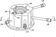
도 1a-1c는 ALD 프로세스들을 위해서 구성된 가스 전달 시스템(130)을 포함하는 프로세스 챔버(100)의 일 실시예의 개략도들이다. 도 1d는 가스 전달 시스템(130)의 다른 실시예를 포함하는 프로세스 챔버(100)의 개략도이다. 프로세스 챔버(100)는 측벽들(104) 및 하단부(106)를 가지는 챔버 바디(102)를 포함한다. 프로세스 챔버(100) 내의 슬릿 밸브(108)는 200 mm 또는 300 mm 반도체 웨이퍼 또는 유리 기판과 같은 기판(110)을 프로세스 챔버(100)로 전달하고 프로세스 챔버(100)로부터 회수(retrieve)하기 위해 로봇(미도시)에 대한 액세스를 제공한다.1A-1C are schematic diagrams of one embodiment of a
기판 지지부(112)는 프로세스 챔버(100) 내의 기판 수용 표면(111) 상에서 기판(110)을 지지한다. 기판 지지부(112)는 기판 지지부(112) 및 그 상부에 배치된 기판(110)을 상승 및 하강시키기 위한 리프트 모터(114)에 장착된다. 리프트 모터(118)에 연결된 리프트 플레이트(116)가 프로세스 챔버(100) 내에 장착되고 그리고 기판 지지부(112)를 통해서 이동가능하게 배치된 리프트 핀들(120)을 상승 및 하강시킨다. 리프트 핀들(120)은 기판 지지부(112)의 표면 위에서 기판(110)을 상승 및 하강시킨다. 기판 지지부(112)는 증착 프로세스 동안에 기판(110)을 기판 지지부(112)에 고정하기 위한 진공 척(미도시), 정전 척(미도시), 또는 클램프 링(미도시)을 포함할 수 있다.The
기판 지지부(112)의 온도는 기판 지지부(112) 상에 배치된 기판(110)의 온도를 제어하기 위해서 조정될 수 있다. 예를 들어, 기판 지지부(112)는 저항성 히터(미도시)와 같은 매립형 가열 엘리먼트를 이용하여 가열될 수 있고, 또는 기판 지지부(112) 위에 배치된 가열 램프들(미도시)과 같은 복사열을 이용하여 가열될 수 있다. 퍼지 링(122)은 기판 지지부(112) 상에 배치되어 퍼지 채널(124)을 형성할 수 있고, 그러한 퍼지 채널은 기판(110)의 주변 부분으로 퍼지 가스를 제공하여 그 주변 부분 상의 증착을 방지한다.The temperature of the
가스 전달 시스템(130)은 프로세스 가스 및/또는 퍼지 가스와 같은 가스를 프로세스 챔버(100)로 제공하기 위해서 챔버 바디(102)의 상부 부분에 배치된다. 도 1a-1d는 기판(110)을 적어도 2개의 가스 소오스들 또는 화학물질 전구체들에 노출시키도록 구성된 가스 전달 시스템(130)을 도시한다. 도 1b는 도 1a의 라인(1B)을 따른 단면도이다. 진공 시스템(178)은 펌핑 채널(179)과 소통하여, 임의의 희망 가스들을 프로세스 챔버(100)로부터 배기하고 그리고 프로세스 챔버(100)의 펌핑 존(166) 내부에서 희망 압력 또는 희망 압력 범위를 유지하는 것을 돕는다.The
일 실시예에서, 가스 전달 시스템(130)은 챔버 리드 조립체(132)의 중앙 부분을 통해서 연장하는 가스 분산 채널(134)을 가지는 챔버 리드 조립체(132)를 포함한다. 가스 분산 채널(134)은 기판 수용 표면(111)을 향해서 수직으로 연장하고 그리고 또한 가스 분산 채널(134)의 중앙 축(133)을 따라서, 리드 플레이트(170)를 통해서, 그리고 하부 표면(160)으로 연장한다. 일 예에서, 가스 분산 채널(134)의 일부는 상부 부분(350) 내에서 중앙 축(133)을 따라서 실질적으로 원통형이고 그리고 가스 분산 채널(134)의 일부는 상기 가스 분산 채널(134)의 하부 부분(135) 내에서 중앙 축(133)으로부터 테이퍼링된다. 가스 분산 채널(134)은 하부 표면(160)을 지나 그리고 반응 존(164)으로 더 연장한다. 하부 표면(160)은 가스 분산 채널(134)의 하부 부분(135)으로부터 초크(162)까지 연장한다. 하부 표면(160)은 기판 지지부(112)의 기판 수용 표면(111) 상에 배치된 기판(110)을 실질적으로 커버하도록 크기 설정되고 형상화된다.In one embodiment, the
프로세싱 가스들은 가스 분산 채널(134)의 중앙 축(133) 주위에서 강제로 회전하게 되는 한편, 분산 채널을 통해서 통과하게 된다. 분산 채널을 통한 프로세스 가스들의 유동을 예증하는 원형 가스 유동들(174)은 소용돌이(vortex) 패턴, 나사선(helix) 패턴, 나선형 패턴, 또는 이들의 파생형 패턴과 같은 여러 가지 타입들의 유동 패턴들을 포함할 수 있다. 원형 가스 유동들(174)은 가스 분산 채널(134)의 중앙 축(133) 주위로 적어도 약 1 회전, 바람직하게는 적어도 약 1.5 회전, 보다 바람직하게는 적어도 약 2 회전, 보다 바람직하게는 적어도 약 3 회전, 및 보다 바람직하게는 약 4 회전 또는 그 초과의 회전으로 연장될 수 있다.The processing gases are forced to rotate about the
상부 부분(350)을 포함하는 가스 분산 채널(134)은 함께 및/또는 별도로 제공될 수 있는 밸브들(142A/152A, 142B/152B)의 2개의 유사한 쌍들로부터 가스 유동들을 제공하기 위한 가스 유입구들(340, 345)을 구비한다. 하나의 구성에서, 밸브(142A) 및 밸브(142B)는 독립적인 반응제 가스 소오스들에 커플링되지만, 바람직하게는 동일한 퍼지 가스 소오스에 커플링된다. 예를 들어, 밸브(142A)는 반응제 가스 소오스(138)에 커플링되고, 그리고 밸브(142B)는 반응제 가스 소오스(139)에 커플링되고, 그리고 양 밸브들(142A, 142B)은 퍼지 가스 소오스(140)에 커플링된다. 각각의 밸브(142A, 142B)는 밸브 시트 조립체(144A, 144B)를 가지는 전달 라인(143A, 143B)을 포함하고, 각각의 밸브(152A, 152B)는 밸브 시트 조립체(146A, 146B)를 가지는 퍼지 라인(145A, 145B)을 포함한다. 전달 라인(143A, 143B)은 반응제 가스 소오스들(138 및 139)과 유체 소통하고 그리고 가스 분산 채널(134)의 가스 유입구들(340, 345)과 유체 소통한다. 전달 라인(143A, 143B)의 밸브 시트 조립체(144A, 144B)는 반응제 가스 소오스들(138 및 139)로부터 가스 분산 채널(134)로의 반응제 가스의 유동을 제어한다. 퍼지 라인(145A, 145B)은 퍼지 가스 소오스(140)와 소통하고 그리고 전달 라인(143A, 143B)의 밸브 시트 조립체(144A, 144B) 하류에서 전달 라인(143A, 143B)과 교차한다. 퍼지 라인(145A, 145B)의 밸브 시트 조립체(146A, 146B)는 퍼지 가스 소오스(140)로부터 가스 분산 채널(134)로의 퍼지 가스의 유동을 제어한다. 만약 반응제 가스 소오스들(138 및 139)로부터 반응제 가스들을 전달하기 위해서 캐리어 가스가 이용된다면, 바람직하게 동일한 가스가 캐리어 가스 및 퍼지 가스로서 이용된다(예를 들어, 아르곤 가스가 캐리어 가스 및 퍼지 가스로서 이용됨).The
각각의 밸브 시트 조립체(144A, 144B, 146A, 146B)는 다이아프램(diaphragm)(미도시) 및 밸브 시트(미도시)를 포함할 수 있다. 그러한 다이아프램은 개방 또는 폐쇄 상태로 바이어스될 수 있고 그리고 각각 폐쇄 또는 개방 상태로 작동될 수 있다. 다이아프램들은 공압식으로 작동될 수 있거나 또는 전기적으로 작동될 수 있다. 공압식으로 작동되는 밸브들은 Fujikin, Inc. 및 Veriflo Division, Parker Hannifin, Corp. 로부터 입수가능한 공압식으로 작동되는 밸브들을 포함한다. 전기적으로 작동되는 밸브들은 Fujikin, Inc. 로부터 입수가능한 전기적으로 작동되는 밸브들을 포함한다. 예를 들어, 이용될 수 있는 ALD 밸브는 Fujikin Model No. FPR-UDDFAT-21-6.35-PI-ASN 또는 Fujikin Model No. FPR-NHDT-21-6.35-PA-AYT이다. 프로그램 가능한 로직 제어기들(148A, 148B)은 밸브들(142A, 142B)에 커플링되어 밸브들(142A, 142B)의 밸브 시트 조립체들(144A, 144B, 146A, 146B)의 다이아프램들의 작동(actuation)을 제어할 수 있다. 공압식으로 작동되는 밸브들은 약 0.020초 만큼 짧은 시간 기간들에 가스들의 펄스들을 제공할 수 있다. 전기적으로 작동되는 밸브들은 약 0.005초만큼 짧은 시간 기간들에 가스들의 펄스들을 제공할 수 있다. 전기적으로 작동되는 밸브는 통상적으로 밸브와 프로그램가능한 로직 제어기 사이에 커플링된 드라이버의 이용을 필요로 한다.Each
밸브 시트 조립체(144A, 144B)가 폐쇄될 때 전달 라인(143A, 143B)으로부터의 반응제 가스의 플러싱(flushing)을 가능하게 하기 위해서 각각의 밸브(142A, 142B)는 제로 데드 부피(zero dead volume; 사공간이 없는) 밸브일 수 있다. 예를 들어, 퍼지 라인(145A, 145B)은 전달 라인(143A, 143B)의 밸브 시트 조립체(144A, 144B) 근처에 위치설정될 수 있다. 밸브 시트 조립체(144A, 144B)가 폐쇄될 때, 퍼지 라인(145A, 145B)이 전달 라인(143A, 143B)을 플러싱하기 위해서 퍼지 가스를 제공할 수 있다. 일 실시예에서, 퍼지 라인(145A, 145B)이 전달 라인(143A, 143B)의 밸브 시트 조립체(144A, 144B)로부터 약간 이격되어 위치설정되어, 개방되었을 때 퍼지 가스가 밸브 시트 조립체(144A, 144B) 내로 직접적으로 전달되지 않는다. 본원에서 사용되는 바와 같은 제로 데드 부피 밸브는 무시할만한 데드 부피를 가지는 밸브로서 규정된다(즉, 반드시 제로 데드 부피인 것은 아니다).To enable flushing of the reactant gases from the
각각의 밸브 쌍(142A/152A, 142B/152B)이 반응제 가스 및 퍼지 가스의 조합된 가스 유동 및/또는 분리된 가스 유동들을 제공하도록 구성될 수 있다. 밸브 쌍(142A/152A)에 관하여, 반응제 가스와 퍼지 가스의 조합된 가스 유동의 일 예가 퍼지 가스 소오스(140)로부터 퍼지 라인(145A)을 통한 퍼지 가스의 연속적인 유동 및 반응제 가스 소오스(138)로부터 전달 라인(143A)을 통한 반응제 가스의 펄스들을 포함한다. 퍼지 가스의 연속적인 유동은 퍼지 라인(145A)의 밸브 시트 조립체(146A)의 다이아프램을 개방된 상태로 놓아둠으로써 제공될 수 있다. 반응제 가스 소오스(138)로부터의 반응제 가스의 펄스들은 전달 라인(143A)의 밸브 시트 조립체(144A)의 다이아프램을 개방 및 폐쇄함으로써 제공될 수 있다. 밸브 쌍(142A/152A)에 관하여, 반응제 가스 및 퍼지 가스의 분리된 가스 유동들의 일 예는 퍼지 가스 소오스(140)로부터 퍼지 라인(145A)을 통한 퍼지 가스의 펄스들 및 반응제 가스 소오스(138)로부터 전달 라인(143A)을 통한 반응제 가스의 펄스들을 포함한다. 퍼지 가스의 펄스들은 퍼지 라인(145A)의 밸브 시트 조립체(146A)의 다이아프램을 개방 및 폐쇄함으로써 제공될 수 있다. 반응제 가스 소오스(138)로부터의 반응제 가스의 펄스들은 전달 라인(143A)의 밸브 시트 조립체(144A)의 다이아프램을 개방 및 폐쇄함으로써 제공될 수 있다.Each
밸브들(142A, 142B)의 전달 라인들(143A, 143B)이 유체 전달 라인들(210, 220) 및 환형 채널들(260, 265)을 통해서 가스 유입구들(340, 345)과 커플링될 수 있다. 유체 전달 라인들(210, 220)은 밸브들(142A, 142B)과 통합될 수 있거나 또는 밸브들로부터 분리될 수 있을 것이며, 그에 따라 하나 또는 그 초과의 유체 소오스들에 연결된다. 일 양상에서, 밸브들(142A, 142B)과 가스 유입구들(340, 345) 사이의 유체 전달 라인들(210, 220) 및 전달 라인(143A, 143B)의 임의의 불필요한 부피를 줄이기 위해서, 밸브들(142A, 142B)이 가스 분산 채널(134)에 가까이 근접하여 커플링된다.The
이론에 의해서 제한되질 않기 바라면서, 가스 분산 채널(134)의 상부 부분(350)으로부터 중앙 축(133)을 따른 어떤 포인트까지 일정하고 그리고 상기 포인트로부터 가스 분산 채널(134)의 하부 부분(135)까지 증가하는 가스 분산 채널(134)의 지름은, 가스 분산 채널(134)을 통한 가스의 적은(less of) 단열(adiabatic) 팽창을 허용하고, 이는 원형 가스 유동(174) 내에 포함된 프로세스 가스의 온도를 제어하는데 도움이 되는 것으로 여겨진다. 예를 들어, 가스 분산 채널(134) 내로 전달된 가스의 갑작스런 단열 팽창은 가스의 온도의 강하를 초래할 수 있고 이는 가스의 응결 및 액적들(droplets)의 형성을 야기할 수 있다. 다른 한편으로, 점진적으로 테이퍼링되는 가스 분산 채널(134)은 가스의 적은 단열 팽창을 제공하는 것으로 여겨진다. 그에 따라, 가스로 그리고 가스로부터 보다 많은 열이 전달될 수 있고, 그에 따라 챔버 리드 조립체(132)의 온도를 제어함으로써 가스의 온도가 더 용이하게 제어될 수 있다. 가스 분산 채널(134)은 점진적으로 테이퍼링될 수 있고 테이퍼형의 직선형 표면, 오목한 표면, 볼록한 표면, 또는 이들의 조합들과 같은 하나 또는 그 초과의 테이퍼형 내측 표면들을 포함할 수 있거나, 또는 하나 또는 그 초과의 테이퍼형 내측 표면들의 섹션들(즉, 테이퍼형 부분 및 비-테이퍼형 부분)을 포함할 수 있다.It is desired that the
도 1d는 도 1b에 도시된 바와 같은 프로세스 챔버(100)와 유사한 도면이고, 그리고 유사한 특징부들 및 컴포넌트들(components)을 포함할 수 있다. 도 1d는 전술한 것과 유사한 밸브들의 쌍들로부터 가스 유동들을 제공하기 위해서 분산 채널(134)의 가스 유입구들(340, 345, 370, 375)과 커플링된 4개의 유체 전달 라인들(210, 215, 220, 225)을 포함하는 가스 전달 시스템(130)의 실시예를 예증한다. 이러한 실시예에서, 상부 부분(350)을 포함하는 가스 분산 채널(134)은 함께 및/또는 독립적으로 제공될 수 있는 밸브들의 쌍들로부터의 가스 유동들을 제공하기 위해서 가스 유입구들(340, 345, 370, 375)의 4개의 세트를 가진다. 밸브들의 전달 라인들은 유체 전달 라인들(210, 215, 220, 225) 및 환형 채널들(260, 265, 270, 275)을 통해서 가스 유입구들(340, 345, 370, 375)과 커플링될 수 있다.FIG. 1D is a view similar to the
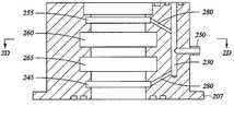
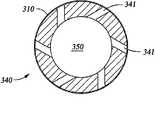
챔버 리드 조립체는 그러한 챔버 리드 조립체의 일부에서 중앙 축을 따라서 연장하고 확장되는 채널(134)을 포함한다. 채널(134)의 상부 부분(350)은 하우징(200) 내에 배치된 삽입체(300)에 의해서 형성된다. 캡(400)이 하우징(200) 및 삽입체(300) 상에 배치될 수 있다.The chamber lid assembly includes a
하우징(200)은 베이스(207) 상에 배치된 환형 매니폴드(205)를 포함할 수 있다. 도 2a-2g에 도시된 바와 같은 실시예들에서, 환형 매니폴드(205)는 내측 구역(290)을 형성하고 상기 내측 구역(290) 주위에 배치된 둘 또는 그 초과의 환형 채널들을 적어도 부분적으로 형성한다. 도 2c는 도 2a의 라인(2C)을 따른 단면도이다. 도 2d는 도 2c의 라인(2D)을 따른 단면도이다. 대안적 실시예에서, 환형 매니폴드(205)는 내측 구역(290)을 형성하고 그리고 상기 내측 구역(290) 주위에 배치된 환형 채널을 포함한다. 도 2f는 3개의 유체 전달 라인들 및 2개의 환형 채널들을 보여주는 다른 실시예이다. 도 2g는 도 2f의 라인(2G)을 따른 단면도이다.The
둘 또는 그 초과의 환형 채널들이 환형 매니폴드(205)의 중앙 축(133)을 따라서 서로로부터 수직으로 이격된 방식으로 배치된다. 환형 채널(260)과 같은 환형 채널은 내부에서 유체를 유동시키도록 구성된 채널을 포함하고, 그리고 내측 구역(290)을 부분적으로 또는 전체적으로 둘러싼다. 환형 채널은 내측 구역에 대해서 360°까지의 유체 소통, 예를 들어 내측 구역 주위로 270°내지 360°의 유체 소통을 제공할 수 있다. 각각의 환형 채널은 환형 매니폴드(205)와 커플링된 삽입체(300) 내에 형성된 개구들을 통해서 유체들을 분산시키기 위해, 프로세싱 가스와 같은 유체가 유체 소오스(예를 들어, 가스 소오스)로부터 내측 구역으로 전달될 수 있게 한다. 각각의 환형 채널들은 여러 가지 단면 형상들 및 디자인들을 가질 수 있다. 예를 들어, 환형 채널은 원형, 반원형, 직사각형, 또는 타원형 단면 디자인일 수 있다. 바람직하게, 단면 디자인은 환형 채널로부터 상기 환형 채널과 커플링된 개구들로 프로세싱 가스와 같은 유체의 효과적인 유동을 제공하도록 구성된다. 예를 들어, 환형 채널은 직사각형 단면의 3개의 면들(sides)을 포함할 수 있고 그리고 제 4 면은 삽입체(300)의 수직 바디(330)일 수 있다. 이러한 방식에서, 3개의 직사각형 횡단면 면들 및 삽입체(300)의 수직 바디(330)의 제 4 면이 함께 환형 채널을 형성한다.Two or more annular channels are disposed in a manner such that they are vertically spaced from each other along the
일 실시예에서, 도 2d 및 2e에 도시된 바와 같이, 각각의 환형 채널은 환형 채널(260)과 같이 내측 구역(290)에 원주방향으로 걸쳐지고(span), 그리고 내측 구역의 360°의 유체 소통을 제공한다. 대안적 실시예에서, 환형 채널들 중 하나가 360°의 유체 소통을 가질 수 있고, 그리고 적어도 제 2 환형 채널이 360°미만의 유체 소통을 가질 수 있다. 일 실시예에서, 제 1 환형 채널(260) 및 제 2 환형 채널(265)이 내측 구역(290) 주위에 배치된다.In one embodiment, as shown in Figures 2d and 2e, each annular channel spans circumferentially in the
하나 또는 그 초과의 카트리지 히터들(240)이 환형 매니폴드(205) 내에 배치될 수 있다. 하우징(200)이 스테인리스 스틸로 제조될 수 있다. 캡(400)이 또한 스테인리스 스틸로 제조될 수 있다.One or
도 1d, 2a, 및 2f에 도시된 바와 같이, 환형 채널들의 각각이 유체 전달 라인들(210, 215, 220, 225)과 같은 각각의 유체 전달 라인과 커플링된다. 대안적으로, 환형 채널들의 각각이, 환형 채널들을 통해서 유동하는 가스들 또는 대안적 가스들의 혼합물을 제공할 수 있는, 도 2f 및 2g에 도시된 바와 같은, 둘 또는 그 초과의 유체 전달 라인들과 커플링될 수 있다. 유체 전달 라인들(210, 215, 및 220)은 환형 채널들(260, 265)과 커플링된다. 도 2g는 환형 채널(265)에 각각 커플링된 유체 전달 라인들(210 및 215)을 도시한다.Each of the annular channels is coupled with a respective fluid delivery line such as
유체 라인들의 각각이 가스 소오스와 같은 유체 소오스와 커플링된다. 대안적으로, 각각의 유체 라인들은 환형 채널들을 통해서 유동하는 가스들 또는 대안적 가스들의 혼합물을 제공할 수 있는 둘 또는 그 초과의 가스 소오스들과 커플링될 수 있다. 복수의 환형 채널들의 이용은, 하프늄 산화물 증착 프로세스에 대해 하프늄 클로라이드 및 물과 같은 상이한 전구체들의 공급을 허용할 수 있고, 및/또는 상이한 농도들을 갖는 동일한 전구체를 허용할 수 있다. 부가적으로, 플레넘(plenum)이 혼합 전구체들 또는 전구체들의 교호적인 전달을 포함하여 상이한 전구체들을 공급할 수 있다.Each of the fluid lines is coupled with a fluid source, such as a gas source. Alternatively, each of the fluid lines may be coupled with two or more gas sources that can provide a mixture of gases or alternate gases flowing through the annular channels. The use of a plurality of annular channels may allow for the supply of different precursors such as hafnium chloride and water for the hafnium oxide deposition process, and / or may allow the same precursor with different concentrations. Additionally, a plenum can supply different precursors, including alternating delivery of mixed precursors or precursors.
퍼지 라인(250)과 같은 하나 이상의 퍼지 라인이 또한 환형 매니폴드(205) 내에 형성될 수 있다. 퍼지 라인은 환형 매니폴드(205)의 수직 부분 내로 도입된다. 퍼지 라인은 하나 또는 그 초과의 갭 퍼지 라인들(280)과 커플링된 수평 가스 수송(transport) 라인을 포함하며, 이는 일련의 환형 채널들의 위와 아래에서 내측 구역(290)과 접촉하도록 배치된다. 내측 구역에서 갭 퍼지 라인들(280)의 각각은 내측 구역 근처에 배치된 환형 매니폴드(205)의 표면에 형성된, 원주방향으로 형성된 환형 채널(245, 255)과 같은, 연장하는 환형 채널을 구비할 수 있다. 퍼지 라인(250)은 또한 환형 매니폴드(205) 내에 배치된 수직으로 배치된 라인(230)과 커플링된다. 하나 또는 그 초과의 갭 퍼지 라인들은 삽입체(300)의 수직 바디(330)를 따라서 근처의 가스 분산 채널(134)을 형성하는 리드 캡(172)의 물질과 삽입체(300) 사이의 물질 교차부(380)까지 퍼지 가스의 유동을 또한 제공한다. 하우징과 삽입체 사이에 배치된, o-링들(385)과 같은 임의의 구조적 밀봉 물질들과 프로세싱 가스들이 반응하는 것을 퍼지 가스가 추가적으로 방지할 것이며, 리드 캡(172)의 하부 물질과 리드 플레이트 조립체는 근처의 가스 분산 채널(134)을 형성한다.One or more purge lines, such as
퍼지 라인(250)은 프로세싱 챔버에 대해서 앞서 설명한 바와 같은 퍼지 가스 소오스들 중 하나에 연결될 수 있고, 그리고 퍼지 가스는 질소 또는 희가스와 같은 비-반응성 가스를 포함할 수 있다. 퍼지 라인은 삽입체들과 환형 매니폴드(205) 사이에 퍼지 가스를 제공하여 그들 영역들(areas) 내에서 원치않는 프로세싱 가스들을 제거한다. 그에 따라, 퍼지 가스는, 금속 할라이드 전구체들과 같은 반응성 프로세싱 가스들에 노출될 때 시간 경과에 따라 열화(degrade)될 수 있는, o-링 물질들과 같은 민감한 물질들을 프로세싱 가스들로부터 보호한다.The
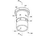
도 3a-3c를 참조하면, 삽입체(300)는 내측 구역(290) 내에 배치되고 그리고 채널(134)의 상부 부분(350)을 형성한다. 삽입체는 하우징(200)의 상단 부분에 커플링되도록 구성된 절두형(truncated) 부분(320)을 가지는 커플링 리드(310), 및 환형 매니폴드(205)의 내에 배치되도록 그리고 그 내부에 대해 플러싱되도록(flushed) 구성된 수직 바디(330)를 포함한다. 바디(330)는 상부 부분(350)을 형성한다. 상부 부분은 원통형 형상 또는 실질적으로 원통형인 형상을 포함할 수 있다. 일 예에서, 도 3b에 도시된 바와 같이, 상부 부분(350)은 원통형 상부 부분(351) 및 확장하는 하단 부분(352)을 포함하고, 상기 확장하는 하단 부분(352)은 복수의 개구들(346)의 하단부 세트 아래에 배치된다.3A-3C, the
하나 또는 그 초과의 가스 유입구들(340, 345)이 삽입체(300)의 수직 바디 내에 배치될 수 있다. 유입구들(340, 345)은 수직 바디(330)의 부분에서 수평 평면을 따라 복수의 개구들(341, 346)을 포함할 수 있으며, 그에 따라 다중-개구 유입구들(340, 345)을 형성할 수 있다. 각각의 수평 평면을 따른 개구들(341, 346)의 개수는 2 내지 10 개의 개구들, 예를 들어, 도 3a-3c에 도시된 바와 같은 6개의 개구들일 수 있다. 복수의 개구들 중 하나 또는 그 초과의 세트들이 삽입체(300)를 따라서 형성될 수 있다. 개구들(341, 346)은 수직 바디(330)의 수평 평면 주위에서 서로로부터 등변으로(equilterally) 배치될 수 있다. 대안적으로, 개구들(341, 346)은 상부 부분(350) 내로 희망하는 가스 유동 특성을 제공하도록 이격되고 및/또는 그룹화될 수 있다. 상부 부분(350)과 협력하여 수직 바디(330)의 수평 평면 주위에서 서로로부터 등변으로 배치된 개구들이 균등(equalization) 홈(groove)들을 형성하여, 각각의 개구들(341, 346)을 통해서 동일한 또는 실질적으로 동일한 압력 및 가스 유량들을 허용함으로써 기판 표면에서 프로세스 가스들의 보다 균일한 유동을 제공하는 것으로 여겨진다.One or
개구들(341, 346)은 중앙 축(133)에 대한 임의의 각도로, 예컨대 수직 바디(330)를 통해서 그리고 중앙 축(133) 또는 가스 분산 채널(134)에 대해서 대략적으로 접선으로 배치될 수 있다. 개구들(341, 346)은 방사상 및 수직 방향들에 대해서 상이한 각도들로 배향될 수 있다. 바람직하게, 개구들(341, 346)은 수평 및/또는 수직 방식으로 0°내지 90°로 각도를 이루어, 원하는 유동 특성을 제공한다. 일 실시예에서, 개구들(341 및 346)은 상부 부분(350)에 대해서 접선을 이루는 각도로, 예컨대, 약 0°내지 약 90°, 바람직하게는 약 0°내지 약 60°, 바람직하게는 약 0°내지 약 45°, 그리고 보다 바람직하게는 약 0°내지 약 20°의 범위 내로 위치설정된다.The
개구들(341, 346)은 환형 매니폴드(205)의 둘 또는 그 초과의 환형 채널들(260, 265)과 유체적으로 커플링되도록 배치된다. 복수의 개구들의 복수의 세트들이 환형 매니폴드(205) 내에 형성된 환형 채널에 대응하는 각각의 유입구와 함께 이용될 수 있다. 개구들은 임의의 단면 형상, 예를 들어, 직사각형 형상, 원통형 튜브 형상, 또는 눈물방울(tear drop) 형상일 수 있다. 복수의 개구들을 가지는 유입구들 및 환형 채널들의 조합이 기판 표면에서 프로세스 가스들의 보다 균일한 유동을 제공하는 것으로 여겨진다.The
삽입체(300)는 금속 할라이드 전구체 가스들과 같은 프로세싱 가스들과 비-반응성인 물질로 제조될 수 있다. 하나의 그러한 물질은 석영이다. 도면들에 도시된 구성에서, 석영 삽입체는 증가된 물질 양립성(compatibility)을 가지는 것으로 관찰되고, 즉 석영 삽입체는 스테인리스 스틸 또는 알루미늄과 같은 다른 물질들보다 할라이드 전구체들, 및 물과 같은 프로세싱 가스들과 더 적은 반응성을 가진다. 추가적으로, 삽입체 물질은 또한 삽입체(300)가 접촉할 수 있는 챔버의 다른 구조적 컴포넌트들과 보다 더 양립적일 수 있다. 예를 들어, 가스 분산 채널(134)을 둘러싸는 리드 플레이트(170)의 부분들 및 리드 캡(172)은 통상적으로 석영으로 제조되고, 석영 삽입체(300)는 양호한 물질 양립성을 가질 것이고 그리고 제조 및 조립에 대해서 더 구조적으로 양립성일 것이다.The
유입구를 형성하는 복수의 개구들(복수의 입구 포인트들)을 가지는 본원에서 설명된 리드 캡은 기판 표면에 걸쳐 프로세싱 가스들의 보다 균일한 유동을 제공하고, 그에 따라 단일 입구 포인트/단일 입구 유입구에 비교하여 환형 방향으로 보다 균일한 두께를 제공하는 것으로 여겨진다. 단일 입구 포인트/단일 입구 유입구와 비교하여, 2 인치 링 분석, 4 인치 링 분석에 따라서 그리고 기판 엣지로부터 3mm에서, 본원에 설명된 리드 캡(172) 조립체의 다중-환형 채널로 개선된 두께 균일성을 갖는 더 얇은(lower) 웨이퍼-인-웨이퍼(WiW) 두께가 달성될 수 있음이 관찰되었다. 앞서, 단일 입구 포인트/단일 입구 유입구에 대해, 기판 엣지로부터 3 mm에서의 기판 부분은 바람직하지 못한 증착 두께 및 균일성을 가지는 침체 존(stagnant zone)이 될 것으로 관찰되었다. 추가적으로, 본원에서 설명된 다중-환형 채널은, 단일 입구 포인트/단일 입구 유입구에 비교하여, 후방 확산 위험을 보다 낮추고, 독립적인 라인들을 통한 프로세싱 가스의 독립적인 제어를 허용하고, 그리고 단일 입구 포인트/단일 입구 유입구에 비교하여 o-링들을 보호하기 위한 가열된 불활성 가스 퍼지를 제공하는 것으로 관찰되었다. 추가적으로, 다중-환형 채널은 부식에 대한 보호를 개선하기 위한 PVD 밸브들의 사용을 허용하고, VCR 피팅들로 대체된 면(face) 밀봉들과 같은 단순화된 하드웨어 디자인을 제공하며, 그리고 단일 입구 포인트/단일 입구 유입구에 대해 필수적인 컴포넌트들을 제거하며, 이는 단일 입구 포인트/단일 입구 유입구에 비교하여 개선된 편리(serviceability)를 허용한다.The lead cap described herein having a plurality of openings (a plurality of inlet points) defining an inlet provides a more uniform flow of the processing gases across the substrate surface, thereby providing a single inlet point / Thereby providing a more uniform thickness in the annular direction. Improved thickness uniformity to a multiple-annular channel of the
도 1a-1b는 본원의 실시예들에서 설명된 바와 같은 가스 분산 채널(134)로의 경로 가스들의 이동을 도시한다. 프로세스 가스들은 유체 전달 라인들(210 및 220)로부터 가스 환형 채널들(260 및 265) 내로, 가스 유입구들(340, 345)을 통해서, 그리고 상부 부분(350) 내로 그리고 가스 분산 채널(134)을 통해서 전달된다. 도 2d, 3b, 및 3c는 프로세스 가스 또는 전구체 가스가 이동하는 경로 즉, 유체 전달 라인(210)으로부터 가스 환형 채널들(265) 내로, 유입구(340)를 통해서, 그리고 상부 부분(350) 내로의 경로를 예증한다. 도 1b, 2d, 3b, 및 3c에 도시된 바와 같이, 제 2 경로는 유체 전달 라인(220)으로부터 가스 환형 채널(260) 내로, 유입구(345)를 통해서, 그리고 상부 부분(350) 내로 연장한다.1A-1B illustrate the movement of path gases into the
도 1b는 통과 가스 유동들의 단순화된 표상들을 도시하는, 챔버 리드 조립체(132)의 가스 분산 채널(134) 및 가스 분산 채널(134)의 상부 부분(350)의 단면도이다. 가스 분산 채널(134)을 통한 정확한 유동 패턴이 알려져 있지는 않지만, 원형 가스 유동(174)(도 1b)이 유입구들(340, 345)로부터 가스 분산 채널(134)을 통해서 소용돌이 유동, 나사선 유동, 나선형 유동, 회전(swirl) 유동, 돌림(twirl) 유동, 트위스트 유동, 코일 유동, 코르크스크류 유동, 컬(curl) 유동, 월풀(whirlpool) 유동, 이들의 파생형 유동들, 또는 이들의 조합들과 같은 원형 유동 패턴으로 이동할 수 있는 것으로 여겨진다. 도 1b에 도시된 바와 같이, 원형 유동은 기판(110)으로부터 분리된 격실 내와 반대되는 것으로서 "프로세싱 구역" 내에 제공될 수 있다. 일 양상에서, 원형 가스 유동(174)은 가스 분산 채널(134)의 내측 표면에 걸친 소용돌이 유동 패턴의 스위핑(sweeping) 작용으로 인한 가스 분산 채널(134)의 보다 효율적인 퍼지를 설정하는 것을 도울 수 있다.1B is a cross-sectional view of the
일 실시예에서, 도 1b는 기판(110)의 표면에서의 포인트(176a)와 가스 분산 채널(134)의 원통형 상부 부분(351)에서의 포인트(176b) 사이의 거리(175)를 도시한다. 기판(110)의 표면에 걸친 나선형 유동이 바람직하지 않을 수 있기 때문에, 원형 가스 유동(174)이 하향 유동으로 소산(dissipate)될 수 있을 정도로 거리(175)가 충분히 길다. 원형 가스 유동(174)이 기판(110) 및 챔버 리드 조립체(132)의 표면을 효율적으로 퍼징하는 층류(laminar) 방식으로 진행하는 것으로 여겨진다. 다른 실시예에서, 중앙 축(133)을 따라서 연장하는 가스 분산 채널(134) 또는 거리(175)가 약 3 인치 내지 약 9 인치, 바람직하게는 약 3.5 인치 내지 약 7 인치, 그리고 보다 바람직하게는 약 4 인치 내지 약 6 인치의 범위 내의 길이, 예를 들어 약 5 인치의 길이를 가진다.1B shows the
도 1a는, 기판(110)의 표면에 걸친(즉, 기판의 중심으로부터 기판의 엣지까지) 가스 분산 채널(134)로부터의 가스 유동의 개선된 속도 프로파일을 제공하는 것을 돕기 위해서, 챔버 리드 조립체(132)의 하부 표면(160)의 적어도 일부가 가스 분산 채널(134)로부터 챔버 리드 조립체(132)의 주변 부분까지 테이퍼링될 수 있다는 것을 도시한다. 하부 표면(160)은 직선형 표면, 오목 표면, 볼록 표면, 또는 이들의 조합들과 같은 하나 또는 그 초과의 테이퍼형 표면들을 포함할 수 있다. 일 실시예에서, 하부 표면(160)은 깔대기 형상으로 테이퍼링된다.1A illustrates a chamber lid assembly (not shown) to assist in providing an improved velocity profile of gas flow from a
일 예에서, 하부 표면(160)은, 반응제 가스에 대한 기판(110)의 표면의 균일한 노출을 제공하는 것을 도우면서, 기판(110)과 챔버 리드 조립체(132)의 하부 표면(160) 사이에서 이동하는 프로세스 가스들의 속도 변동을 줄이는 것을 돕기 위해서 하향 경사진다. 일 실시예에서, 기판(110)의 표면과 챔버 리드 조립체(132)의 하향 경사 하부 표면(160) 사이의 유동 섹션의 최소 영역(area)에 대한 유동 섹션의 최대 영역의 비율은 약 2 미만, 바람직하게는 약 1.5 미만, 보다 바람직하게는 약 1.3 미만, 그리고 보다 바람직하게는 약 1 이다.In one example, the
이론에 의해서 제한되질 않기 바라면서, 기판(110)의 표면에 걸쳐 더욱 균일한 속도로 이동하는 가스 유동이 기판(110) 상에서의 가스의 보다 균일한 증착을 제공하는 것을 돕는 것으로 여겨진다. 가스의 속도는 가스의 농도에 직접적으로 비례하고, 그러한 가스의 농도는 또한 기판(110) 표면 상의 가스의 증착 레이트에 직접적으로 비례하는 것으로 여겨진다. 따라서, 기판(110)의 표면의 제 2 영역에 대비한(versus) 기판(110)의 표면의 제 1 영역에서의 가스의 보다 높은 속도가 제 1 영역 상에서 가스의 보다 빠른(higher) 증착을 제공하는 것으로 여겨진다. 하향 경사진 하부 표면(160)을 가지는 챔버 리드 조립체(132)가 기판(110)의 표면에 걸친 가스의 보다 균일한 증착을 제공하는 것으로 믿어지는데, 이는 하부 표면(160)이 기판(110)의 표면에 걸친 가스의 보다 균일한 속도 및 그에 따라 보다 균일한 농도를 제공하기 때문이다.It is believed that a gas flow that moves at a more uniform rate across the surface of the
또한, 본원 발명의 실시예들에 따라서 기판을 프로세싱하기 위한 여러 가지 방법들이 채용될 수 있다. 일 실시예에서, 기판을 프로세싱하는 방법은 가스 소오스들(138, 139)과 같은 하나 또는 그 초과의 유체 소오스들로부터 챔버 리드 조립체(132)의 유체 전달 라인들(210, 220)을 통해서 둘 또는 그 초과의 프로세스 가스들을 유동시키는 단계, 및 유체 전달 라인들(210, 220)로부터 챔버 리드 조립체(132)의 하우징(200)에 의해서 적어도 부분적으로 형성되는 둘 또는 그 초과의 환형 채널들(260, 265)을 통해서 둘 또는 그 초과의 프로세스 가스들을 유동시키는 단계를 포함한다. 하우징은 내측 구역(290)을 가진다. 둘 또는 그 초과의 프로세스 가스들이 둘 또는 그 초과의 환형 채널들(260, 265)로부터 내측 구역(290) 내에 배치된 삽입체(300)를 통해서 그리고 챔버 리드 조립체(132) 내의 채널(134)의 상부 부분(350) 내로 유동된다. 삽입체(300)는 채널(134)의 상부 부분(350)을 형성한다. 하나 또는 그 초과의 프로세스 가스들이 채널(134)을 통해서 그리고 기판 지지부(112) 상에 배치된 기판(110) 위의 반응 존(164) 내로 유동된다.In addition, various methods for processing substrates in accordance with embodiments of the present invention may be employed. In one embodiment, a method of processing a substrate may be performed from one or more fluid sources, such as
도 1a는 기판(110)의 주변부 근처의 챔버 리드 조립체(132)의 주변 부분에 위치된 쵸크(162)를 도시한다. 쵸크(162)는, 챔버 리드 조립체(132)가 조립되어 기판(110) 주위의 프로세싱 존을 형성할 때, 기판(110)의 주변부 근처의 영역에서 가스가 통과하여 유동하는 것을 제한하는 임의의 부재를 포함한다.1A shows a
하나의 특정 실시예에서, 쵸크(162)와 기판 지지부(112) 사이의 간격은 약 0.04 인치 내지 약 2.0 인치이고, 그리고 바람직하게 0.04 인치 내지 약 0.2 인치이다. 간격은 증착 동안의 프로세스 조건들 및 전달되는 가스들에 따라서 달라질 수 있다. 쵸크(162)는 반응 존(164)을 펌핑 존(166)(도 1a)의 불균일 압력 분포로부터 격리시킴으로써 챔버 리드 조립체(132)와 기판(110) 사이에 형성된 부피 또는 반응 존(164) 내의 보다 균일한 압력 분포를 제공하는데 도움이 된다.In one particular embodiment, the spacing between the
도 1a를 참조하면, 일 양상에서, 반응 존(164)이 펌핑 존(166)으로부터 격리되기 때문에, 반응제 가스 또는 퍼지 가스에 대한 기판(110)의 충분한 노출을 보장하기 위해서 반응제 가스 또는 퍼지 가스는 반응 존(164)을 단지 적절하게만 채울 필요가 있다. 종래의 화학 기상 증착에서, 종래 기술의 챔버들은, 기판(110)의 표면에 걸쳐 반응제들의 상호-반응(co-reaction)이 균일하게 발생하도록 보장하기 위해서, 기판의 전체 표면에 대해서 동시적으로 그리고 균일하게 반응제들의 조합된 유동을 제공하도록 요구된다. 원자 층 증착에서, 프로세스 챔버(100)는 기판(110)의 표면으로 순차적으로 반응제들을 도입하여, 기판(110)의 표면 상으로 반응제들의 교호적인 얇은 층들의 흡수를 제공한다. 결과적으로, 원자 층 증착은 기판(110)의 표면에 동시에 도달하는 반응제의 유동을 필요로 하지 않는다. 그 대신에, 기판(110)의 표면 상에서 반응제의 얇은 층을 흡착하기에 충분한 양으로 반응제의 유동이 제공될 필요가 있다.Referring to FIG. 1A, in one aspect, the reactive gas or purge
반응 존(164)이 종래의 CVD 챔버의 내측 부피와 비교하여, 보다 작은 부피를 포함할 수 있기 때문에, 원자 층 증착 시퀀스에서의 특정 프로세스를 위해서 반응 존(164)을 채우는데 있어서 보다 적은 양의 가스가 요구된다. 예를 들어, 일 실시예에서, 200 mm 지름의 기판들을 프로세싱하도록 구성된 챔버에 대해 반응 존(164)의 부피는 약 1,000 cm3 또는 그 미만, 바람직하게 500 cm3 또는 그 미만, 그리고 보다 바람직하게 200 cm3 또는 그 미만이다. 일 실시예에서, 300 mm 지름의 기판들을 프로세싱하도록 구성된 챔버에 대해 반응 존(164)의 부피는 약 3,000 cm3 또는 그 미만, 바람직하게 1,500 cm3 또는 그 미만, 그리고 보다 바람직하게 600 cm3 또는 그 미만이다. 일 실시예에서, 기판 지지부(112)는 증착을 위한 반응 존(164)의 부피를 조정하기 위해서 상승되거나 하강될 수 있다. 반응 존(164)의 보다 적은 부피로 인해서, 증착 가스이든지 또는 퍼지 가스이든지 간에, 보다 적은 가스가 프로세스 챔버(100) 내로 유동될 필요가 있다. 따라서, 이용되는 가스의 양이 더 적기 때문에 프로세스 챔버(100)의 수율이 보다 커지고 그리고 폐기물이 최소화될 수 있어, 운영 비용이 감소된다.Because the
리드 캡(172) 및 리드 플레이트(170)를 포함하는 것으로서 챔버 리드 조립체(132)가 도 1a-1b에 도시되어 있으며, 여기에서 리드 캡(172) 및 리드 플레이트(170)가 가스 분산 채널(134)을 형성한다. 일 실시예에서, 프로세스 챔버(100)는 도 1a-1b에 도시된 바와 같이 가스 환형 채널들(260 및 265)을 구비하는 하우징(200)을 포함하는 리드 캡(172)을 포함한다. 부가적인 플레이트가 리드 플레이트(170)와 리드 캡(172)(미도시) 사이에 선택적으로 배치될 수 있다. 부가적인 플레이트는 리드 캡(172)과 리드 플레이트(170) 사이의 거리를 조정하는(예를 들어, 증가시키는)데 사용될 수 있어, 그에 따라 관통하여 형성된 분산 채널(134)의 길이를 각각 변화시킬 수 있다. 다른 실시예에서, 리드 플레이트(170)와 리드 캡(172) 사이에 배치된 선택적인 부가적 플레이트는 스테인리스 스틸을 포함한다. 다른 실시예들에서, 가스 분산 채널(134)은 단일 피스의 물질로 일체로 제조될 수 있다.1A-1B in which a
챔버 리드 조립체(132)는 관통하여 전달되는 특정 가스에 따라 냉각 엘리먼트들 및/또는 가열 엘리먼트들을 포함할 수 있다. 챔버 리드 조립체(132) 상에서의 가스 분해, 증착 또는 응결을 방지하기 위해서, 챔버 리드 조립체(132)의 온도를 제어하는 것이 이용될 수 있다. 예를 들어, 챔버 리드 조립체(132)를 냉각시키기 위해서 물 채널들(미도시)이 챔버 리드 조립체(132) 내에 형성될 수 있다. 다른 예에서, 챔버 리드 조립체(132)를 가열하기 위해서 가열 엘리먼트들(미도시)이 챔버 리드 조립체(132)의 컴포넌트들을 둘러쌀 수 있거나 그 내부에 매립될 수 있다. 일 실시예에서, 챔버 리드 조립체(132)의 컴포넌트들이 개별적으로 가열 또는 냉각될 수 있다. 예를 들어, 도 1a를 참조하면, 챔버 리드 조립체(132)는 리드 플레이트(170) 및 리드 캡(172)을 포함할 수 있고, 여기에서 리드 플레이트(170) 및 리드 캡(172)은 가스 분산 채널(134)을 형성한다. 리드 캡(172)은 하나의 온도 범위에서 유지될 수 있고, 그리고 리드 플레이트(170)는 다른 온도 범위에서 유지될 수 있다. 예를 들어, 반응제 가스들의 응결을 방지하기 위해서 리드 캡(172)은 히터 테입 내에서 랩핑됨으로써 또는 다른 가열 디바이스를 이용함으로써 가열될 수 있고, 그리고 리드 플레이트(170)는 상온(ambient temperature)에서 유지될 수 있다. 다른 예에서, 리드 캡(172)은 가열될 수 있고 그리고 리드 플레이트(170) 상에서 반응제 가스들의 열적 분해를 방해하기 위해서 관통하여 형성된 물 채널들을 이용하여 리드 플레이트(170)가 냉각될 수 있다.The
챔버 리드 조립체(132)의 컴포넌트들 및 부분들은 스테인리스 스틸, 알루미늄, 니켈-도금된 알루미늄, 니켈, 이들의 합금들, 또는 다른 적합한 물질들과 같은 물질들을 포함할 수 있다. 일 실시예에서, 리드 캡(172) 및 리드 플레이트(170)는 알루미늄, 알루미늄 합금, 스틸, 스테인리스 스틸, 이들의 합금들, 또는 이들의 조합들과 같은 금속으로부터 독립적으로 제조되고, 기계가공되고, 단조(forge)되고, 또는 다르게 만들어질 수 있다.The components and portions of
일 실시예에서, 챔버 리드 조립체(132)의 하부 표면(160) 및 가스 분산 채널(134)을 따른 가스의 층류 유동을 생성하는 것을 돕기 위해서, 가스 분산 채널(134)의 내측 표면(131)(리드 캡(172) 및 리드 플레이트(170)의 내측 표면들 모두를 포함) 및 챔버 리드 조립체(132)의 하부 표면(160)은 거울 연마된(mirror polished) 표면을 포함할 수 있다. 다른 실시예에서, 유체 전달 라인들(210 및 220)의 내측 표면은 관통하는 가스의 층류 유동을 생성하는 것을 돕기 위해서 전기연마될 수 있다.In one embodiment, to assist in creating a laminar flow of gas along the
대안적 실시예에서, 표면들에 걸쳐서 보다 큰 표면 영역을 생성하기 위해서, 가스 분산 채널(134)의 내측 표면(131)(리드 캡(172) 및 리드 플레이트(170)의 내측 표면들 모두를 포함) 및 챔버 리드 조립체(132)의 하부 표면(160)은 거칠어진 표면 또는 기계가공된 표면들을 포함할 수 있다. 거칠어진 표면들은 내측 표면(131) 및 하부 표면(160) 상에서 원치 않는 축적된 물질들의 보다 우수한 부착을 제공한다. 일반적으로, 원치 않는 필름들은 기상 증착 프로세스 실시의 결과로서 형성되고, 그리고 내측 표면(131) 및 하부 표면(160)으로부터 벗겨지거나 박편되어, 기판(110)을 오염시킬 수 있다. 일 예에서, 하부 표면(160) 및/또는 내측 표면(131)의 평균 조도(Ra)가 적어도 약 10 μin, 예컨대, 약 10 μin (약 0.254 ㎛) 내지 약 200 μin (약 5.08 ㎛), 바람직하게 약 20 μin (약 0.508 ㎛) 내지 약 100 μin (약 2.54 ㎛), 그리고 보다 바람직하게 약 30 μin (약 0.762 ㎛) 내지 약 80 μin (약 2.032 ㎛) 이내일 수 있다. 다른 예에서, 하부 표면(160) 및/또는 내측 표면(131)의 평균 조도는 적어도 약 100 μin (약 2.54 ㎛), 바람직하게 약 200 μin (약 5.08 ㎛) 내지 약 500 μin (약 12.7 ㎛) 범위 이내일 수 있다.In an alternative embodiment, the
도 1a는 프로세싱 조건들을 제어하기 위해서 프로세스 챔버(100)에 커플링된 프로그램된 개인용 컴퓨터, 또는 워크 스테이션 컴퓨터 등과 같은 제어 유닛(180)을 도시한다. 예를 들어, 제어 유닛(180)은 기판 프로세스 시퀀스의 상이한 스테이지들 동안에 가스 소오스들(138, 139 및 140)로부터 밸브들(142A 및 142B)을 통해서 여러 가지 프로세스 가스들 및 퍼지 가스들의 유동을 제어하도록 구성될 수 있다. 예시적으로, 제어 유닛(180)은 중앙처리유닛(CPU)(182), 지원 회로(184), 및 연관된 제어 소프트웨어(183)를 포함하는 메모리(186)를 포함한다.Figure 1A illustrates a
제어 유닛(180)은 여러 가지 챔버들 및 하위-프로세서들을 제어하기 위한 산업적인 셋팅에서 사용될 수 있는 임의의 형태의 범용 컴퓨터 프로세서 중 하나일 수 있다. CPU(182)는, 근거리 또는 원거리의, 랜덤 액세스 메모리, 리드 온리 메모리, 플로피 디스크 드라이브, 하드 디스크, 또는 임의의 다른 형태의 디지털 저장장치와 같은 임의의 적합한 메모리(186)를 이용할 수 있다. 다양한 지원 회로들이 프로세스 챔버(100)를 지원하기 위해 CPU(182)에 커플링될 수 있다. 제어 유닛(180)이 밸브들(142A, 142B)의 프로그램가능한 로직 제어기들(148A, 148B)과 같은 개별적인 챔버 컴포넌트들 근처에 위치된 다른 제어기에 커플링될 수 있다. 제어 유닛(180)과 프로세스 챔버(100)의 다양한 다른 컴포넌트들 사이의 양-방향 통신들은 도 1a에 그 중 일부가 예증된 신호 버스들(188)로서 집합적으로 지칭되는 많은 수의 신호 케이블들을 통해서 핸들링된다. 밸브들(142A, 142B)의 프로그램가능한 로직 제어기들(148A, 148B)로부터 그리고 가스 소오스들(138, 139, 140)로부터의 프로세스 가스들 및 퍼지 가스들을 제어하는 것에 더하여, 제어 유닛(180)은 웨이퍼 프로세싱에서 이용되는 다른 동작들, 예컨대, 다른 동작들 중에서도, 웨이퍼 이송, 온도 제어, 챔버 배기의 자동화된 제어를 책임지도록 구성될 수 있으며, 상기 동작들 중 일부는 본 명세서의 다른 부분에서 설명된다.The
도 1a-1b를 참조하면, 작업 중에, 기판(110)은 로봇(미도시)에 의해서 슬릿 밸브(108)를 통해서 프로세스 챔버(100)로 전달된다. 기판(110)은 리프트 핀들(120)과 로봇의 협력을 통해서 기판 지지부(112) 상에 위치설정된다. 기판 지지부(112)는 기판(110)을 챔버 리드 조립체(132)의 하부 표면(160)에 대해서 근접하여 대향되도록 상승시킨다. 제 2 가스 유동이 밸브(142B)에 의해서 프로세스 챔버(100) 내로 인젝트되는 것과 함께 또는 그와 독립적으로(즉, 펄스들), 제 1 가스 유동은 밸브(142A)에 의해서 프로세스 챔버(100)의 가스 분산 채널(134) 내로 인젝트될 수 있다. 제 1 가스 유동은 퍼지 가스 소오스(140)로부터의 퍼지 가스의 연속적인 유동 및 반응제 가스 소오스(138)로부터의 반응제 가스의 펄스들을 포함할 수 있거나, 또는 반응제 가스 소오스(138)로부터의 반응제 가스의 펄스들 및 퍼지 가스 소오스(140)로부터의 퍼지 가스의 펄스들을 포함할 수 있다. 제 2 가스 유동은 퍼지 가스 소오스(140)로부터의 퍼지 가스의 연속적인 유동 및 반응제 가스 소오스(139)로부터의 반응제 가스의 펄스들을 포함할 수 있거나, 또는 반응제 가스 소오스(139)로부터의 반응제 가스의 펄스들 및 퍼지 가스 소오스(140)로부터의 퍼지 가스의 펄스들을 포함할 수 있다.1A-1B, during operation, the
원형 가스 유동(174)은 소용돌이 유동으로서 가스 분산 채널(134)을 통해서 이동하고, 이는 가스 분산 채널(134)의 내측 표면을 가로지르는 스위핑 작용을 제공한다. 원형 가스 유동(174)은 기판(110)의 표면을 향한 하향 유동으로 소산된다. 가스 유동이 가스 분산 채널(134)을 통해서 이동함에 따라서, 가스 유동의 속도는 감소된다. 이어서, 가스 유동은 기판(110)의 표면을 가로질러 그리고 챔버 리드 조립체(132)의 하부 표면(160)을 가로질러 이동한다. 하향 경사진 챔버 리드 조립체(132)의 하부 표면(160)은 기판(110)의 표면에 걸친 가스 유동의 속도의 변동을 감소시키는데 도움이 된다. 이어서, 가스 유동은 쵸크(162)에 의하여 프로세스 챔버(100)의 펌핑 존(166) 내로 이동한다. 과다 가스, 부산물 등은 펌핑 채널(179) 내로 유동하고, 그리고 이어서 진공 시스템(178)에 의해서 프로세스 챔버(100)로부터 배기된다. 일 양상에서, 가스 유동은 가스 분산 채널(134)을 통해서 그리고 기판(110)의 표면과 챔버 리드 조립체(132)의 하부 표면(160) 사이로 층류 방식으로 진행하고, 그러한 층류 방식은 기판(110)의 표면에 대한 반응제 가스의 균일한 노출을 돕고 그리고 챔버 리드 조립체(132)의 내측 표면들의 효율적인 퍼징을 돕는다.The
도 1a-1b에 예증된 바와 같이, 프로세스 챔버(100)는 특징들의 조합을 가지는 것으로서 여기에서 설명되었다. 일 양상에서, 프로세스 챔버(100)는 종래의 CVD 챔버에 비교하여 작은 부피를 가지는 반응 존(164)을 제공한다. 프로세스 챔버(100)는 특정 프로세스를 위해서 반응 존(164)을 채우기 위한 반응제 가스 또는 퍼지 가스와 같은 가스의 보다 적은 양을 필요로 한다. 다른 양상에서, 프로세스 챔버(100)는 기판(110)과 챔버 리드 조립체(132)의 하단 표면 사이에서 이동하는 가스 유동의 속도 프로파일의 변동을 줄이기 위해서 하향 경사진 또는 깔대기 형상의 하부 표면(160)을 가지는 챔버 리드 조립체(132)를 제공한다. 또 다른 양상에서, 프로세스 챔버(100)는 관통하여 도입되는 가스 유동의 속도를 줄이기 위해서 가스 분산 채널(134)을 제공한다. 또 다른 양상에서, 프로세스 챔버(100)는 가스 분산 채널(134)의 중심으로부터 각도(α)로 유체 전달 라인들을 제공한다. 프로세스 챔버(100)는 본원 명세서의 다른 부분에서 설명된 바와 같은 다른 특징들을 제공한다. 원자 층 증착을 위해 구성된 챔버의 다른 실시예들은 하나 또는 그 초과의 이러한 특징들을 포함한다.1A-1B, the
전술한 내용은 본원 발명의 바람직한 실시예와 관련된 것이지만, 본원 발명의 다른 실시예들 및 추가적인 실시예들은 본원 발명의 기본적인 범위로부터 벗어나지 않고도 안출될 수 있을 것이고, 본원 발명의 범위는 이어지는 청구항들에 의해서 결정된다.While the foregoing is directed to preferred embodiments of the present invention, other and further embodiments of the invention may be devised without departing from the basic scope thereof, and the scope of the present invention is to be defined by the following claims .
Claims (18)
Translated fromKorean리드 및 삽입체(insert)를 포함하며, 상기 리드는:
상부 부분 및 하부 부분을 가지며 상기 리드의 중앙 축을 따라서 연장하는 채널;
내측 구역을 가지고 그리고 상기 채널을 둘러싸는 둘 또는 셋 이상의 환형 채널을 적어도 부분적으로 형성하는 하우징; 및
상기 채널의 하부 부분으로부터 상기 챔버 리드 조립체의 주변 부분까지 연장하는 테이퍼형(tapered) 하단 표면;을 포함하고,
상기 삽입체는, 절두형(truncated) 부분을 갖는 커플링 리드를 포함하며, 상기 삽입체는 상기 채널의 상부 부분 내로 원하는 가스 유동 특성을 제공하기 위해 상기 채널의 상부 부분을 형성하도록 구성되고, 상기 삽입체는 상기 삽입체의 내부에 형성되는 복수의 개구를 가지고, 상기 삽입체는 상기 내측 구역 내에 배치되며, 상기 복수의 개구는 상기 둘 또는 셋 이상의 환형 채널과 유체적으로 커플링되는,
챔버 리드 조립체.A chamber lid assembly comprising:
A lead and an insert, the lead comprising:
A channel having an upper portion and a lower portion and extending along a central axis of the lead;
A housing at least partially defining two or more annular channels with an inner zone and surrounding the channel; And
And a tapered bottom surface extending from a lower portion of the channel to a peripheral portion of the chamber lid assembly,
Wherein the insert comprises a coupling lead having a truncated portion and the insert is configured to form an upper portion of the channel to provide a desired gas flow characteristic into the upper portion of the channel, Wherein the insert has a plurality of openings formed in the interior of the insert, the insert is disposed within the inner region, and the plurality of openings are fluidly coupled with the two or more annular channels.
Chamber lid assembly.
상기 하우징은 베이스 상에 배치된 환형 매니폴드를 더 포함하고, 상기 환형 매니폴드는 상기 내측 구역을 형성하는, 챔버 리드 조립체.The method according to claim 1,
Wherein the housing further comprises an annular manifold disposed on the base, the annular manifold defining the inner section.
상기 둘 또는 셋 이상의 환형 채널은 상기 중앙 축을 따라 수직으로 이격된 방식으로 배치되는, 챔버 리드 조립체.3. The method of claim 2,
Wherein the two or more annular channels are disposed in a vertically spaced manner along the central axis.
상기 환형 매니폴드 내에 배치된 퍼지 라인을 더 포함하는, 챔버 리드 조립체.3. The method of claim 2,
Further comprising a purge line disposed within the annular manifold.
상기 퍼지 라인은 상기 내측 구역과 유체적으로 커플링되는 하나 또는 둘 이상의 갭 퍼지 라인과 커플링된 수평 가스 이송 라인을 포함하는, 챔버 리드 조립체.5. The method of claim 4,
Wherein the purge line comprises a horizontal gas transfer line coupled with one or more gap purge lines that are fluidly coupled to the inner zone.
하나 이상의 갭 퍼지 라인은 상기 둘 또는 셋 이상의 환형 채널 위에서 상기 내측 구역과 커플링되고, 하나 이상의 갭 퍼지 라인은 상기 둘 또는 셋 이상의 환형 채널 아래에서 상기 내측 구역과 커플링되는, 챔버 리드 조립체.6. The method of claim 5,
Wherein one or more gap purge lines are coupled with the inner zone over the two or more annular channels and one or more gap purge lines are coupled with the inner zone below the two or more annular channels.
각각의 갭 퍼지 라인은 상기 내측 구역에 걸쳐지는(span) 원주방향으로 형성된 환형 채널을 더 포함하는, 챔버 리드 조립체.6. The method of claim 5,
Wherein each gap purge line further comprises a circumferentially formed annular channel spanning the inner zone.
상기 퍼지 라인은 상기 환형 매니폴드 내에 배치되는 수직으로 배치된 라인을 더 포함하는, 챔버 리드 조립체.6. The method of claim 5,
Wherein the purge line further comprises a vertically disposed line disposed within the annular manifold.
상기 절두형 부분을 가지는 상기 커플링 리드는 상기 하우징의 상단 부분에 커플링되도록 구성되며, 상기 삽입체는 상기 환형 매니폴드의 내부에 배치되도록 그리고 상기 환형 매니폴드의 내부에 대해 플러싱하도록(flush) 구성되고 상기 채널의 상부 부분을 적어도 부분적으로 형성하는 수직 바디를 더 포함하는, 챔버 리드 조립체.3. The method of claim 2,
Wherein the coupling lead having the truncated portion is configured to be coupled to an upper portion of the housing, the insert being configured to be disposed within the annular manifold and to flush against the interior of the annular manifold, Further comprising a vertical body constructed and at least partially defining an upper portion of the channel.
상기 삽입체는 각각의 환형 채널과 커플링되도록 그리고 각각의 환형 채널과 상기 상부 부분 사이에 다중-개구 유입구를 제공하도록 상기 수직 바디를 통해 수평 평면을 따라 배치된 상기 복수의 개구의 하나 또는 둘 이상의 세트를 더 포함하는, 챔버 리드 조립체.10. The method of claim 9,
Wherein the insert has one or more of the plurality of openings disposed along the horizontal plane through the vertical body to couple with the respective annular channel and to provide a multi-aperture inlet between each annular channel and the upper section. The chamber lid assembly further comprising:
상기 복수의 개구의 세트 각각이 상기 중앙 축을 따라 서로 수직으로 배치되는, 챔버 리드 조립체.11. The method of claim 10,
Each of the plurality of sets of apertures being disposed perpendicular to one another along the central axis.
상기 채널의 상부 부분은 상기 수직 바디에 의해서 원통형 형상을 포함하도록 형성되는, 챔버 리드 조립체.10. The method of claim 9,
Wherein an upper portion of the channel is formed to include a cylindrical shape by the vertical body.
상기 삽입체의 수직 바디는 원통형 상부 부분 및 확장형 하단 부분을 더 포함하고, 상기 확장형 하단 부분은 복수의 개구의 하단부 세트 아래에 배치되는, 챔버 리드 조립체.13. The method of claim 12,
Wherein the vertical body of the insert further comprises a cylindrical upper portion and an expandable lower portion, wherein the expandable lower portion is disposed below a lower set of the plurality of openings.
상기 복수의 개구의 하단부 세트는 2 내지 10개의 개구를 포함하는, 챔버 리드 조립체.14. The method of claim 13,
Wherein the lower set of the plurality of openings comprises 2 to 10 openings.
각각의 개구는 상기 수직 바디로부터 수평으로 0° 내지 60°로 배치되고 상기 수직 바디로부터 수직으로 0° 내지 60°로 배치되는, 챔버 리드 조립체.10. The method of claim 9,
Each opening being disposed horizontally 0 to 60 degrees from the vertical body and 0 to 60 degrees vertically from the vertical body.
각각의 환형 채널은 유체 전달 라인과 커플링되고, 각각의 유체 전달 라인은 하나 또는 둘 이상의 유체 소오스에 커플링되는, 챔버 리드 조립체.The method according to claim 1,
Wherein each annular channel is coupled to a fluid delivery line, and wherein each fluid delivery line is coupled to one or more fluid sources.
각각의 환형 채널은 상기 내측 구역에 원주방향으로 걸쳐지고, 360°의 유체 연통을 제공하는, 챔버 리드 조립체.The method according to claim 1,
Each annular channel spanning circumferentially in the inner zone and providing 360 ° fluid communication.
각각의 개구는 직사각형 형상, 원통형 튜브 형상, 또는 눈물방울(tear drop) 형상인, 챔버 리드 조립체.The method according to claim 1,
Each opening having a rectangular shape, a cylindrical tube shape, or a tear drop shape.
Applications Claiming Priority (3)
| Application Number | Priority Date | Filing Date | Title |
|---|---|---|---|
| US31357310P | 2010-03-12 | 2010-03-12 | |
| US61/313,573 | 2010-03-12 | ||
| PCT/US2011/027599WO2011112617A2 (en) | 2010-03-12 | 2011-03-08 | Atomic layer deposition chamber with multi inject |
Publications (2)
| Publication Number | Publication Date |
|---|---|
| KR20130030745A KR20130030745A (en) | 2013-03-27 |
| KR101810532B1true KR101810532B1 (en) | 2017-12-19 |
Family
ID=44560249
Family Applications (1)
| Application Number | Title | Priority Date | Filing Date |
|---|---|---|---|
| KR1020127026518AActiveKR101810532B1 (en) | 2010-03-12 | 2011-03-08 | Atomic layer deposition chamber with multi inject |
Country Status (8)
| Country | Link |
|---|---|
| US (1) | US9175394B2 (en) |
| EP (1) | EP2545197B1 (en) |
| JP (1) | JP5889806B2 (en) |
| KR (1) | KR101810532B1 (en) |
| CN (1) | CN102762767B (en) |
| SG (2) | SG183536A1 (en) |
| TW (1) | TWI576460B (en) |
| WO (1) | WO2011112617A2 (en) |
Families Citing this family (423)
| Publication number | Priority date | Publication date | Assignee | Title |
|---|---|---|---|---|
| US8291857B2 (en) | 2008-07-03 | 2012-10-23 | Applied Materials, Inc. | Apparatuses and methods for atomic layer deposition |
| US10378106B2 (en) | 2008-11-14 | 2019-08-13 | Asm Ip Holding B.V. | Method of forming insulation film by modified PEALD |
| US9394608B2 (en) | 2009-04-06 | 2016-07-19 | Asm America, Inc. | Semiconductor processing reactor and components thereof |
| US8802201B2 (en) | 2009-08-14 | 2014-08-12 | Asm America, Inc. | Systems and methods for thin-film deposition of metal oxides using excited nitrogen-oxygen species |
| US9312155B2 (en) | 2011-06-06 | 2016-04-12 | Asm Japan K.K. | High-throughput semiconductor-processing apparatus equipped with multiple dual-chamber modules |
| US10854498B2 (en) | 2011-07-15 | 2020-12-01 | Asm Ip Holding B.V. | Wafer-supporting device and method for producing same |
| US20130023129A1 (en) | 2011-07-20 | 2013-01-24 | Asm America, Inc. | Pressure transmitter for a semiconductor processing environment |
| US9017481B1 (en) | 2011-10-28 | 2015-04-28 | Asm America, Inc. | Process feed management for semiconductor substrate processing |
| US9574268B1 (en) | 2011-10-28 | 2017-02-21 | Asm America, Inc. | Pulsed valve manifold for atomic layer deposition |
| US9659799B2 (en) | 2012-08-28 | 2017-05-23 | Asm Ip Holding B.V. | Systems and methods for dynamic semiconductor process scheduling |
| US9132436B2 (en) | 2012-09-21 | 2015-09-15 | Applied Materials, Inc. | Chemical control features in wafer process equipment |
| US10714315B2 (en) | 2012-10-12 | 2020-07-14 | Asm Ip Holdings B.V. | Semiconductor reaction chamber showerhead |
| US20160376700A1 (en) | 2013-02-01 | 2016-12-29 | Asm Ip Holding B.V. | System for treatment of deposition reactor |
| US10256079B2 (en) | 2013-02-08 | 2019-04-09 | Applied Materials, Inc. | Semiconductor processing systems having multiple plasma configurations |
| CN106304597B (en)* | 2013-03-12 | 2019-05-10 | 应用材料公司 | Multi-zone gas injection assembly with azimuthal and radial distribution control |
| WO2014149200A1 (en)* | 2013-03-15 | 2014-09-25 | Applied Materials, Inc. | Plasma reactor with highly symmetrical four-fold gas injection |
| KR102156795B1 (en)* | 2013-05-15 | 2020-09-17 | 에이에스엠 아이피 홀딩 비.브이. | Deposition apparatus |
| US20150004798A1 (en)* | 2013-06-28 | 2015-01-01 | Lam Research Corporation | Chemical deposition chamber having gas seal |
| US10781516B2 (en) | 2013-06-28 | 2020-09-22 | Lam Research Corporation | Chemical deposition chamber having gas seal |
| WO2015047832A1 (en)* | 2013-09-26 | 2015-04-02 | Veeco Ald Inc. | Printing of colored pattern using atommic layer deposition |
| US10683571B2 (en)* | 2014-02-25 | 2020-06-16 | Asm Ip Holding B.V. | Gas supply manifold and method of supplying gases to chamber using same |
| US10167557B2 (en) | 2014-03-18 | 2019-01-01 | Asm Ip Holding B.V. | Gas distribution system, reactor including the system, and methods of using the same |
| US11015245B2 (en) | 2014-03-19 | 2021-05-25 | Asm Ip Holding B.V. | Gas-phase reactor and system having exhaust plenum and components thereof |
| DE102014106523A1 (en) | 2014-05-09 | 2015-11-12 | Aixtron Se | Apparatus and method for supplying a CVD or PVD coating device with a process gas mixture |
| US20150345019A1 (en)* | 2014-05-30 | 2015-12-03 | Applied Materials, Inc. | Method and apparatus for improving gas flow in a substrate processing chamber |
| US10487399B2 (en)* | 2014-06-26 | 2019-11-26 | Applied Materials, Inc. | Atomic layer deposition chamber with counter-flow multi inject |
| US10858737B2 (en) | 2014-07-28 | 2020-12-08 | Asm Ip Holding B.V. | Showerhead assembly and components thereof |
| JP5792364B1 (en)* | 2014-07-31 | 2015-10-07 | 株式会社日立国際電気 | Substrate processing apparatus, chamber lid assembly, semiconductor device manufacturing method, program, and recording medium |
| US10113232B2 (en) | 2014-07-31 | 2018-10-30 | Lam Research Corporation | Azimuthal mixer |
| US9890456B2 (en) | 2014-08-21 | 2018-02-13 | Asm Ip Holding B.V. | Method and system for in situ formation of gas-phase compounds |
| US10407771B2 (en)* | 2014-10-06 | 2019-09-10 | Applied Materials, Inc. | Atomic layer deposition chamber with thermal lid |
| US10941490B2 (en) | 2014-10-07 | 2021-03-09 | Asm Ip Holding B.V. | Multiple temperature range susceptor, assembly, reactor and system including the susceptor, and methods of using the same |
| US9657845B2 (en) | 2014-10-07 | 2017-05-23 | Asm Ip Holding B.V. | Variable conductance gas distribution apparatus and method |
| US9355922B2 (en) | 2014-10-14 | 2016-05-31 | Applied Materials, Inc. | Systems and methods for internal surface conditioning in plasma processing equipment |
| US9966240B2 (en) | 2014-10-14 | 2018-05-08 | Applied Materials, Inc. | Systems and methods for internal surface conditioning assessment in plasma processing equipment |
| US11637002B2 (en) | 2014-11-26 | 2023-04-25 | Applied Materials, Inc. | Methods and systems to enhance process uniformity |
| US9951421B2 (en)* | 2014-12-10 | 2018-04-24 | Lam Research Corporation | Inlet for effective mixing and purging |
| KR102263121B1 (en) | 2014-12-22 | 2021-06-09 | 에이에스엠 아이피 홀딩 비.브이. | Semiconductor device and manufacuring method thereof |
| US10529542B2 (en) | 2015-03-11 | 2020-01-07 | Asm Ip Holdings B.V. | Cross-flow reactor and method |
| US10276355B2 (en) | 2015-03-12 | 2019-04-30 | Asm Ip Holding B.V. | Multi-zone reactor, system including the reactor, and method of using the same |
| US10954597B2 (en)* | 2015-03-17 | 2021-03-23 | Asm Ip Holding B.V. | Atomic layer deposition apparatus |
| JP6487747B2 (en)* | 2015-03-26 | 2019-03-20 | 株式会社Screenホールディングス | Substrate processing apparatus and processing gas supply nozzle |
| JP5961297B1 (en)* | 2015-03-26 | 2016-08-02 | 株式会社日立国際電気 | Substrate processing apparatus, semiconductor device manufacturing method, and program |
| JP6545053B2 (en)* | 2015-03-30 | 2019-07-17 | 東京エレクトロン株式会社 | Processing apparatus and processing method, and gas cluster generating apparatus and generating method |
| WO2016158054A1 (en)* | 2015-03-30 | 2016-10-06 | 東京エレクトロン株式会社 | Treatment device and treatment method, and gas cluster generation device and generation method |
| US11384432B2 (en)* | 2015-04-22 | 2022-07-12 | Applied Materials, Inc. | Atomic layer deposition chamber with funnel-shaped gas dispersion channel and gas distribution plate |
| US10458018B2 (en) | 2015-06-26 | 2019-10-29 | Asm Ip Holding B.V. | Structures including metal carbide material, devices including the structures, and methods of forming same |
| US10600673B2 (en) | 2015-07-07 | 2020-03-24 | Asm Ip Holding B.V. | Magnetic susceptor to baseplate seal |
| US9741593B2 (en) | 2015-08-06 | 2017-08-22 | Applied Materials, Inc. | Thermal management systems and methods for wafer processing systems |
| US9691645B2 (en) | 2015-08-06 | 2017-06-27 | Applied Materials, Inc. | Bolted wafer chuck thermal management systems and methods for wafer processing systems |
| US10504700B2 (en) | 2015-08-27 | 2019-12-10 | Applied Materials, Inc. | Plasma etching systems and methods with secondary plasma injection |
| US9960072B2 (en) | 2015-09-29 | 2018-05-01 | Asm Ip Holding B.V. | Variable adjustment for precise matching of multiple chamber cavity housings |
| US10211308B2 (en) | 2015-10-21 | 2019-02-19 | Asm Ip Holding B.V. | NbMC layers |
| KR102678733B1 (en)* | 2015-12-04 | 2024-06-26 | 어플라이드 머티어리얼스, 인코포레이티드 | Advanced coating methods and materials to prevent HDP-CVD chamber arcing |
| US11139308B2 (en) | 2015-12-29 | 2021-10-05 | Asm Ip Holding B.V. | Atomic layer deposition of III-V compounds to form V-NAND devices |
| US10468251B2 (en) | 2016-02-19 | 2019-11-05 | Asm Ip Holding B.V. | Method for forming spacers using silicon nitride film for spacer-defined multiple patterning |
| US10529554B2 (en) | 2016-02-19 | 2020-01-07 | Asm Ip Holding B.V. | Method for forming silicon nitride film selectively on sidewalls or flat surfaces of trenches |
| US10343920B2 (en) | 2016-03-18 | 2019-07-09 | Asm Ip Holding B.V. | Aligned carbon nanotubes |
| US10865475B2 (en) | 2016-04-21 | 2020-12-15 | Asm Ip Holding B.V. | Deposition of metal borides and silicides |
| US10190213B2 (en) | 2016-04-21 | 2019-01-29 | Asm Ip Holding B.V. | Deposition of metal borides |
| US10367080B2 (en) | 2016-05-02 | 2019-07-30 | Asm Ip Holding B.V. | Method of forming a germanium oxynitride film |
| US10032628B2 (en) | 2016-05-02 | 2018-07-24 | Asm Ip Holding B.V. | Source/drain performance through conformal solid state doping |
| US10504754B2 (en) | 2016-05-19 | 2019-12-10 | Applied Materials, Inc. | Systems and methods for improved semiconductor etching and component protection |
| US11453943B2 (en) | 2016-05-25 | 2022-09-27 | Asm Ip Holding B.V. | Method for forming carbon-containing silicon/metal oxide or nitride film by ALD using silicon precursor and hydrocarbon precursor |
| US10662527B2 (en) | 2016-06-01 | 2020-05-26 | Asm Ip Holding B.V. | Manifolds for uniform vapor deposition |
| JP6756853B2 (en)* | 2016-06-03 | 2020-09-16 | アプライド マテリアルズ インコーポレイテッドApplied Materials,Incorporated | Effective and new design for low particle count and better wafer quality by diffusing the flow inside the chamber |
| KR102553629B1 (en)* | 2016-06-17 | 2023-07-11 | 삼성전자주식회사 | Plasma processing apparatus |
| JP6696322B2 (en)* | 2016-06-24 | 2020-05-20 | 東京エレクトロン株式会社 | Gas processing apparatus, gas processing method and storage medium |
| US10388509B2 (en) | 2016-06-28 | 2019-08-20 | Asm Ip Holding B.V. | Formation of epitaxial layers via dislocation filtering |
| US9865484B1 (en) | 2016-06-29 | 2018-01-09 | Applied Materials, Inc. | Selective etch using material modification and RF pulsing |
| US10612137B2 (en) | 2016-07-08 | 2020-04-07 | Asm Ip Holdings B.V. | Organic reactants for atomic layer deposition |
| US9859151B1 (en) | 2016-07-08 | 2018-01-02 | Asm Ip Holding B.V. | Selective film deposition method to form air gaps |
| US10714385B2 (en) | 2016-07-19 | 2020-07-14 | Asm Ip Holding B.V. | Selective deposition of tungsten |
| KR102532607B1 (en) | 2016-07-28 | 2023-05-15 | 에이에스엠 아이피 홀딩 비.브이. | Substrate processing apparatus and method of operating the same |
| US9812320B1 (en) | 2016-07-28 | 2017-11-07 | Asm Ip Holding B.V. | Method and apparatus for filling a gap |
| US10395919B2 (en) | 2016-07-28 | 2019-08-27 | Asm Ip Holding B.V. | Method and apparatus for filling a gap |
| US9887082B1 (en) | 2016-07-28 | 2018-02-06 | Asm Ip Holding B.V. | Method and apparatus for filling a gap |
| US10629473B2 (en) | 2016-09-09 | 2020-04-21 | Applied Materials, Inc. | Footing removal for nitride spacer |
| US10546729B2 (en) | 2016-10-04 | 2020-01-28 | Applied Materials, Inc. | Dual-channel showerhead with improved profile |
| US10410943B2 (en) | 2016-10-13 | 2019-09-10 | Asm Ip Holding B.V. | Method for passivating a surface of a semiconductor and related systems |
| US10643826B2 (en) | 2016-10-26 | 2020-05-05 | Asm Ip Holdings B.V. | Methods for thermally calibrating reaction chambers |
| US11532757B2 (en) | 2016-10-27 | 2022-12-20 | Asm Ip Holding B.V. | Deposition of charge trapping layers |
| US10435790B2 (en) | 2016-11-01 | 2019-10-08 | Asm Ip Holding B.V. | Method of subatmospheric plasma-enhanced ALD using capacitively coupled electrodes with narrow gap |
| US10714350B2 (en) | 2016-11-01 | 2020-07-14 | ASM IP Holdings, B.V. | Methods for forming a transition metal niobium nitride film on a substrate by atomic layer deposition and related semiconductor device structures |
| US10229833B2 (en) | 2016-11-01 | 2019-03-12 | Asm Ip Holding B.V. | Methods for forming a transition metal nitride film on a substrate by atomic layer deposition and related semiconductor device structures |
| US10643904B2 (en) | 2016-11-01 | 2020-05-05 | Asm Ip Holdings B.V. | Methods for forming a semiconductor device and related semiconductor device structures |
| US10134757B2 (en) | 2016-11-07 | 2018-11-20 | Asm Ip Holding B.V. | Method of processing a substrate and a device manufactured by using the method |
| US10163696B2 (en) | 2016-11-11 | 2018-12-25 | Applied Materials, Inc. | Selective cobalt removal for bottom up gapfill |
| US10026621B2 (en) | 2016-11-14 | 2018-07-17 | Applied Materials, Inc. | SiN spacer profile patterning |
| KR102546317B1 (en) | 2016-11-15 | 2023-06-21 | 에이에스엠 아이피 홀딩 비.브이. | Gas supply unit and substrate processing apparatus including the same |
| US10340135B2 (en) | 2016-11-28 | 2019-07-02 | Asm Ip Holding B.V. | Method of topologically restricted plasma-enhanced cyclic deposition of silicon or metal nitride |
| KR102762543B1 (en) | 2016-12-14 | 2025-02-05 | 에이에스엠 아이피 홀딩 비.브이. | Substrate processing apparatus |
| US11447861B2 (en) | 2016-12-15 | 2022-09-20 | Asm Ip Holding B.V. | Sequential infiltration synthesis apparatus and a method of forming a patterned structure |
| US11581186B2 (en) | 2016-12-15 | 2023-02-14 | Asm Ip Holding B.V. | Sequential infiltration synthesis apparatus |
| KR102700194B1 (en) | 2016-12-19 | 2024-08-28 | 에이에스엠 아이피 홀딩 비.브이. | Substrate processing apparatus |
| US10269558B2 (en) | 2016-12-22 | 2019-04-23 | Asm Ip Holding B.V. | Method of forming a structure on a substrate |
| US10867788B2 (en) | 2016-12-28 | 2020-12-15 | Asm Ip Holding B.V. | Method of forming a structure on a substrate |
| US11390950B2 (en) | 2017-01-10 | 2022-07-19 | Asm Ip Holding B.V. | Reactor system and method to reduce residue buildup during a film deposition process |
| RU172394U1 (en)* | 2017-01-13 | 2017-07-06 | Федеральное государственное автономное образовательное учреждение высшего образования "Национальный исследовательский университет "Московский институт электронной техники" | ATOMIC LAYER DEPOSITION DEVICE |
| US10431429B2 (en) | 2017-02-03 | 2019-10-01 | Applied Materials, Inc. | Systems and methods for radial and azimuthal control of plasma uniformity |
| US10655221B2 (en) | 2017-02-09 | 2020-05-19 | Asm Ip Holding B.V. | Method for depositing oxide film by thermal ALD and PEALD |
| US10468261B2 (en) | 2017-02-15 | 2019-11-05 | Asm Ip Holding B.V. | Methods for forming a metallic film on a substrate by cyclical deposition and related semiconductor device structures |
| US10943834B2 (en) | 2017-03-13 | 2021-03-09 | Applied Materials, Inc. | Replacement contact process |
| US10529563B2 (en) | 2017-03-29 | 2020-01-07 | Asm Ip Holdings B.V. | Method for forming doped metal oxide films on a substrate by cyclical deposition and related semiconductor device structures |
| USD876504S1 (en) | 2017-04-03 | 2020-02-25 | Asm Ip Holding B.V. | Exhaust flow control ring for semiconductor deposition apparatus |
| KR102457289B1 (en) | 2017-04-25 | 2022-10-21 | 에이에스엠 아이피 홀딩 비.브이. | Method for depositing a thin film and manufacturing a semiconductor device |
| US10770286B2 (en) | 2017-05-08 | 2020-09-08 | Asm Ip Holdings B.V. | Methods for selectively forming a silicon nitride film on a substrate and related semiconductor device structures |
| US10446393B2 (en) | 2017-05-08 | 2019-10-15 | Asm Ip Holding B.V. | Methods for forming silicon-containing epitaxial layers and related semiconductor device structures |
| US10892156B2 (en) | 2017-05-08 | 2021-01-12 | Asm Ip Holding B.V. | Methods for forming a silicon nitride film on a substrate and related semiconductor device structures |
| US11276559B2 (en) | 2017-05-17 | 2022-03-15 | Applied Materials, Inc. | Semiconductor processing chamber for multiple precursor flow |
| US11276590B2 (en) | 2017-05-17 | 2022-03-15 | Applied Materials, Inc. | Multi-zone semiconductor substrate supports |
| JP7176860B6 (en) | 2017-05-17 | 2022-12-16 | アプライド マテリアルズ インコーポレイテッド | Semiconductor processing chamber to improve precursor flow |
| US10504742B2 (en) | 2017-05-31 | 2019-12-10 | Asm Ip Holding B.V. | Method of atomic layer etching using hydrogen plasma |
| US10886123B2 (en) | 2017-06-02 | 2021-01-05 | Asm Ip Holding B.V. | Methods for forming low temperature semiconductor layers and related semiconductor device structures |
| US10920320B2 (en) | 2017-06-16 | 2021-02-16 | Applied Materials, Inc. | Plasma health determination in semiconductor substrate processing reactors |
| US12040200B2 (en) | 2017-06-20 | 2024-07-16 | Asm Ip Holding B.V. | Semiconductor processing apparatus and methods for calibrating a semiconductor processing apparatus |
| US11306395B2 (en) | 2017-06-28 | 2022-04-19 | Asm Ip Holding B.V. | Methods for depositing a transition metal nitride film on a substrate by atomic layer deposition and related deposition apparatus |
| US10685834B2 (en) | 2017-07-05 | 2020-06-16 | Asm Ip Holdings B.V. | Methods for forming a silicon germanium tin layer and related semiconductor device structures |
| US10727080B2 (en) | 2017-07-07 | 2020-07-28 | Applied Materials, Inc. | Tantalum-containing material removal |
| KR20190009245A (en) | 2017-07-18 | 2019-01-28 | 에이에스엠 아이피 홀딩 비.브이. | Methods for forming a semiconductor device structure and related semiconductor device structures |
| US10541333B2 (en) | 2017-07-19 | 2020-01-21 | Asm Ip Holding B.V. | Method for depositing a group IV semiconductor and related semiconductor device structures |
| US11018002B2 (en) | 2017-07-19 | 2021-05-25 | Asm Ip Holding B.V. | Method for selectively depositing a Group IV semiconductor and related semiconductor device structures |
| US11374112B2 (en) | 2017-07-19 | 2022-06-28 | Asm Ip Holding B.V. | Method for depositing a group IV semiconductor and related semiconductor device structures |
| US10590535B2 (en) | 2017-07-26 | 2020-03-17 | Asm Ip Holdings B.V. | Chemical treatment, deposition and/or infiltration apparatus and method for using the same |
| US10605530B2 (en) | 2017-07-26 | 2020-03-31 | Asm Ip Holding B.V. | Assembly of a liner and a flange for a vertical furnace as well as the liner and the vertical furnace |
| TWI815813B (en) | 2017-08-04 | 2023-09-21 | 荷蘭商Asm智慧財產控股公司 | Showerhead assembly for distributing a gas within a reaction chamber |
| US10297458B2 (en) | 2017-08-07 | 2019-05-21 | Applied Materials, Inc. | Process window widening using coated parts in plasma etch processes |
| US10692741B2 (en) | 2017-08-08 | 2020-06-23 | Asm Ip Holdings B.V. | Radiation shield |
| US10770336B2 (en) | 2017-08-08 | 2020-09-08 | Asm Ip Holding B.V. | Substrate lift mechanism and reactor including same |
| US11139191B2 (en) | 2017-08-09 | 2021-10-05 | Asm Ip Holding B.V. | Storage apparatus for storing cassettes for substrates and processing apparatus equipped therewith |
| US10249524B2 (en) | 2017-08-09 | 2019-04-02 | Asm Ip Holding B.V. | Cassette holder assembly for a substrate cassette and holding member for use in such assembly |
| US11769682B2 (en) | 2017-08-09 | 2023-09-26 | Asm Ip Holding B.V. | Storage apparatus for storing cassettes for substrates and processing apparatus equipped therewith |
| USD900036S1 (en) | 2017-08-24 | 2020-10-27 | Asm Ip Holding B.V. | Heater electrical connector and adapter |
| US11830730B2 (en) | 2017-08-29 | 2023-11-28 | Asm Ip Holding B.V. | Layer forming method and apparatus |
| US11056344B2 (en) | 2017-08-30 | 2021-07-06 | Asm Ip Holding B.V. | Layer forming method |
| KR102491945B1 (en) | 2017-08-30 | 2023-01-26 | 에이에스엠 아이피 홀딩 비.브이. | Substrate processing apparatus |
| US11295980B2 (en) | 2017-08-30 | 2022-04-05 | Asm Ip Holding B.V. | Methods for depositing a molybdenum metal film over a dielectric surface of a substrate by a cyclical deposition process and related semiconductor device structures |
| KR102401446B1 (en) | 2017-08-31 | 2022-05-24 | 에이에스엠 아이피 홀딩 비.브이. | Substrate processing apparatus |
| US10607895B2 (en) | 2017-09-18 | 2020-03-31 | Asm Ip Holdings B.V. | Method for forming a semiconductor device structure comprising a gate fill metal |
| KR102630301B1 (en) | 2017-09-21 | 2024-01-29 | 에이에스엠 아이피 홀딩 비.브이. | Method of sequential infiltration synthesis treatment of infiltrateable material and structures and devices formed using same |
| US10844484B2 (en) | 2017-09-22 | 2020-11-24 | Asm Ip Holding B.V. | Apparatus for dispensing a vapor phase reactant to a reaction chamber and related methods |
| US10658205B2 (en) | 2017-09-28 | 2020-05-19 | Asm Ip Holdings B.V. | Chemical dispensing apparatus and methods for dispensing a chemical to a reaction chamber |
| US10403504B2 (en) | 2017-10-05 | 2019-09-03 | Asm Ip Holding B.V. | Method for selectively depositing a metallic film on a substrate |
| US10319588B2 (en) | 2017-10-10 | 2019-06-11 | Asm Ip Holding B.V. | Method for depositing a metal chalcogenide on a substrate by cyclical deposition |
| US10923344B2 (en) | 2017-10-30 | 2021-02-16 | Asm Ip Holding B.V. | Methods for forming a semiconductor structure and related semiconductor structures |
| CN107699865B (en)* | 2017-11-10 | 2024-04-19 | 西安鑫垚陶瓷复合材料股份有限公司 | Device for uniformly feeding air for vapor deposition furnace |
| US10910262B2 (en) | 2017-11-16 | 2021-02-02 | Asm Ip Holding B.V. | Method of selectively depositing a capping layer structure on a semiconductor device structure |
| KR102443047B1 (en) | 2017-11-16 | 2022-09-14 | 에이에스엠 아이피 홀딩 비.브이. | Method of processing a substrate and a device manufactured by the same |
| US11022879B2 (en) | 2017-11-24 | 2021-06-01 | Asm Ip Holding B.V. | Method of forming an enhanced unexposed photoresist layer |
| CN111344522B (en) | 2017-11-27 | 2022-04-12 | 阿斯莫Ip控股公司 | Including clean mini-environment device |
| WO2019103613A1 (en) | 2017-11-27 | 2019-05-31 | Asm Ip Holding B.V. | A storage device for storing wafer cassettes for use with a batch furnace |
| US10903054B2 (en) | 2017-12-19 | 2021-01-26 | Applied Materials, Inc. | Multi-zone gas distribution systems and methods |
| US11328909B2 (en) | 2017-12-22 | 2022-05-10 | Applied Materials, Inc. | Chamber conditioning and removal processes |
| US10854426B2 (en) | 2018-01-08 | 2020-12-01 | Applied Materials, Inc. | Metal recess for semiconductor structures |
| US10872771B2 (en) | 2018-01-16 | 2020-12-22 | Asm Ip Holding B. V. | Method for depositing a material film on a substrate within a reaction chamber by a cyclical deposition process and related device structures |
| TWI799494B (en) | 2018-01-19 | 2023-04-21 | 荷蘭商Asm 智慧財產控股公司 | Deposition method |
| KR102695659B1 (en) | 2018-01-19 | 2024-08-14 | 에이에스엠 아이피 홀딩 비.브이. | Method for depositing a gap filling layer by plasma assisted deposition |
| USD903477S1 (en) | 2018-01-24 | 2020-12-01 | Asm Ip Holdings B.V. | Metal clamp |
| US11018047B2 (en) | 2018-01-25 | 2021-05-25 | Asm Ip Holding B.V. | Hybrid lift pin |
| USD880437S1 (en) | 2018-02-01 | 2020-04-07 | Asm Ip Holding B.V. | Gas supply plate for semiconductor manufacturing apparatus |
| US10535516B2 (en) | 2018-02-01 | 2020-01-14 | Asm Ip Holdings B.V. | Method for depositing a semiconductor structure on a surface of a substrate and related semiconductor structures |
| US11081345B2 (en) | 2018-02-06 | 2021-08-03 | Asm Ip Holding B.V. | Method of post-deposition treatment for silicon oxide film |
| US10896820B2 (en) | 2018-02-14 | 2021-01-19 | Asm Ip Holding B.V. | Method for depositing a ruthenium-containing film on a substrate by a cyclical deposition process |
| WO2019158960A1 (en) | 2018-02-14 | 2019-08-22 | Asm Ip Holding B.V. | A method for depositing a ruthenium-containing film on a substrate by a cyclical deposition process |
| US10731249B2 (en) | 2018-02-15 | 2020-08-04 | Asm Ip Holding B.V. | Method of forming a transition metal containing film on a substrate by a cyclical deposition process, a method for supplying a transition metal halide compound to a reaction chamber, and related vapor deposition apparatus |
| US10679870B2 (en) | 2018-02-15 | 2020-06-09 | Applied Materials, Inc. | Semiconductor processing chamber multistage mixing apparatus |
| US10964512B2 (en) | 2018-02-15 | 2021-03-30 | Applied Materials, Inc. | Semiconductor processing chamber multistage mixing apparatus and methods |
| US10658181B2 (en) | 2018-02-20 | 2020-05-19 | Asm Ip Holding B.V. | Method of spacer-defined direct patterning in semiconductor fabrication |
| KR102636427B1 (en) | 2018-02-20 | 2024-02-13 | 에이에스엠 아이피 홀딩 비.브이. | Substrate processing method and apparatus |
| US10975470B2 (en) | 2018-02-23 | 2021-04-13 | Asm Ip Holding B.V. | Apparatus for detecting or monitoring for a chemical precursor in a high temperature environment |
| TWI766433B (en) | 2018-02-28 | 2022-06-01 | 美商應用材料股份有限公司 | Systems and methods to form airgaps |
| US11473195B2 (en) | 2018-03-01 | 2022-10-18 | Asm Ip Holding B.V. | Semiconductor processing apparatus and a method for processing a substrate |
| US10593560B2 (en) | 2018-03-01 | 2020-03-17 | Applied Materials, Inc. | Magnetic induction plasma source for semiconductor processes and equipment |
| US11629406B2 (en) | 2018-03-09 | 2023-04-18 | Asm Ip Holding B.V. | Semiconductor processing apparatus comprising one or more pyrometers for measuring a temperature of a substrate during transfer of the substrate |
| US10319600B1 (en) | 2018-03-12 | 2019-06-11 | Applied Materials, Inc. | Thermal silicon etch |
| US11114283B2 (en) | 2018-03-16 | 2021-09-07 | Asm Ip Holding B.V. | Reactor, system including the reactor, and methods of manufacturing and using same |
| KR102646467B1 (en) | 2018-03-27 | 2024-03-11 | 에이에스엠 아이피 홀딩 비.브이. | Method of forming an electrode on a substrate and a semiconductor device structure including an electrode |
| US10510536B2 (en) | 2018-03-29 | 2019-12-17 | Asm Ip Holding B.V. | Method of depositing a co-doped polysilicon film on a surface of a substrate within a reaction chamber |
| US11088002B2 (en) | 2018-03-29 | 2021-08-10 | Asm Ip Holding B.V. | Substrate rack and a substrate processing system and method |
| US11230766B2 (en) | 2018-03-29 | 2022-01-25 | Asm Ip Holding B.V. | Substrate processing apparatus and method |
| KR102501472B1 (en) | 2018-03-30 | 2023-02-20 | 에이에스엠 아이피 홀딩 비.브이. | Substrate processing method |
| KR102535194B1 (en)* | 2018-04-03 | 2023-05-22 | 주성엔지니어링(주) | Apparatus for Processing Substrate |
| KR102600229B1 (en) | 2018-04-09 | 2023-11-10 | 에이에스엠 아이피 홀딩 비.브이. | Substrate supporting device, substrate processing apparatus including the same and substrate processing method |
| US10699879B2 (en) | 2018-04-17 | 2020-06-30 | Applied Materials, Inc. | Two piece electrode assembly with gap for plasma control |
| US10886137B2 (en) | 2018-04-30 | 2021-01-05 | Applied Materials, Inc. | Selective nitride removal |
| US12025484B2 (en) | 2018-05-08 | 2024-07-02 | Asm Ip Holding B.V. | Thin film forming method |
| TWI811348B (en) | 2018-05-08 | 2023-08-11 | 荷蘭商Asm 智慧財產控股公司 | Methods for depositing an oxide film on a substrate by a cyclical deposition process and related device structures |
| US12272527B2 (en) | 2018-05-09 | 2025-04-08 | Asm Ip Holding B.V. | Apparatus for use with hydrogen radicals and method of using same |
| KR20190129718A (en) | 2018-05-11 | 2019-11-20 | 에이에스엠 아이피 홀딩 비.브이. | Methods for forming a doped metal carbide film on a substrate and related semiconductor device structures |
| KR102596988B1 (en) | 2018-05-28 | 2023-10-31 | 에이에스엠 아이피 홀딩 비.브이. | Method of processing a substrate and a device manufactured by the same |
| TWI840362B (en) | 2018-06-04 | 2024-05-01 | 荷蘭商Asm Ip私人控股有限公司 | Wafer handling chamber with moisture reduction |
| US11718913B2 (en) | 2018-06-04 | 2023-08-08 | Asm Ip Holding B.V. | Gas distribution system and reactor system including same |
| US11286562B2 (en) | 2018-06-08 | 2022-03-29 | Asm Ip Holding B.V. | Gas-phase chemical reactor and method of using same |
| KR102568797B1 (en) | 2018-06-21 | 2023-08-21 | 에이에스엠 아이피 홀딩 비.브이. | Substrate processing system |
| US10797133B2 (en) | 2018-06-21 | 2020-10-06 | Asm Ip Holding B.V. | Method for depositing a phosphorus doped silicon arsenide film and related semiconductor device structures |
| TWI873894B (en) | 2018-06-27 | 2025-02-21 | 荷蘭商Asm Ip私人控股有限公司 | Cyclic deposition methods for forming metal-containing material and films and structures including the metal-containing material |
| KR102854019B1 (en) | 2018-06-27 | 2025-09-02 | 에이에스엠 아이피 홀딩 비.브이. | Periodic deposition method for forming a metal-containing material and films and structures comprising the metal-containing material |
| KR102686758B1 (en) | 2018-06-29 | 2024-07-18 | 에이에스엠 아이피 홀딩 비.브이. | Method for depositing a thin film and manufacturing a semiconductor device |
| US10612136B2 (en) | 2018-06-29 | 2020-04-07 | ASM IP Holding, B.V. | Temperature-controlled flange and reactor system including same |
| US10388513B1 (en) | 2018-07-03 | 2019-08-20 | Asm Ip Holding B.V. | Method for depositing silicon-free carbon-containing film as gap-fill layer by pulse plasma-assisted deposition |
| US10755922B2 (en) | 2018-07-03 | 2020-08-25 | Asm Ip Holding B.V. | Method for depositing silicon-free carbon-containing film as gap-fill layer by pulse plasma-assisted deposition |
| US10872778B2 (en) | 2018-07-06 | 2020-12-22 | Applied Materials, Inc. | Systems and methods utilizing solid-phase etchants |
| US10755941B2 (en) | 2018-07-06 | 2020-08-25 | Applied Materials, Inc. | Self-limiting selective etching systems and methods |
| US10767789B2 (en) | 2018-07-16 | 2020-09-08 | Asm Ip Holding B.V. | Diaphragm valves, valve components, and methods for forming valve components |
| US10672642B2 (en) | 2018-07-24 | 2020-06-02 | Applied Materials, Inc. | Systems and methods for pedestal configuration |
| US10483099B1 (en) | 2018-07-26 | 2019-11-19 | Asm Ip Holding B.V. | Method for forming thermally stable organosilicon polymer film |
| US11053591B2 (en) | 2018-08-06 | 2021-07-06 | Asm Ip Holding B.V. | Multi-port gas injection system and reactor system including same |
| US10883175B2 (en) | 2018-08-09 | 2021-01-05 | Asm Ip Holding B.V. | Vertical furnace for processing substrates and a liner for use therein |
| US10829852B2 (en) | 2018-08-16 | 2020-11-10 | Asm Ip Holding B.V. | Gas distribution device for a wafer processing apparatus |
| US11430674B2 (en) | 2018-08-22 | 2022-08-30 | Asm Ip Holding B.V. | Sensor array, apparatus for dispensing a vapor phase reactant to a reaction chamber and related methods |
| KR102707956B1 (en) | 2018-09-11 | 2024-09-19 | 에이에스엠 아이피 홀딩 비.브이. | Method for deposition of a thin film |
| US11024523B2 (en) | 2018-09-11 | 2021-06-01 | Asm Ip Holding B.V. | Substrate processing apparatus and method |
| US11049755B2 (en) | 2018-09-14 | 2021-06-29 | Applied Materials, Inc. | Semiconductor substrate supports with embedded RF shield |
| US11049751B2 (en) | 2018-09-14 | 2021-06-29 | Asm Ip Holding B.V. | Cassette supply system to store and handle cassettes and processing apparatus equipped therewith |
| US10892198B2 (en) | 2018-09-14 | 2021-01-12 | Applied Materials, Inc. | Systems and methods for improved performance in semiconductor processing |
| US11062887B2 (en) | 2018-09-17 | 2021-07-13 | Applied Materials, Inc. | High temperature RF heater pedestals |
| US11417534B2 (en) | 2018-09-21 | 2022-08-16 | Applied Materials, Inc. | Selective material removal |
| CN109306470A (en)* | 2018-09-29 | 2019-02-05 | 北京北方华创微电子装备有限公司 | Air inlet device and atomic layer deposition device for atomic layer deposition process |
| CN110970344B (en) | 2018-10-01 | 2024-10-25 | Asmip控股有限公司 | Substrate holding apparatus, system comprising the same and method of using the same |
| US11232963B2 (en) | 2018-10-03 | 2022-01-25 | Asm Ip Holding B.V. | Substrate processing apparatus and method |
| KR102592699B1 (en) | 2018-10-08 | 2023-10-23 | 에이에스엠 아이피 홀딩 비.브이. | Substrate support unit and apparatuses for depositing thin film and processing the substrate including the same |
| US11682560B2 (en) | 2018-10-11 | 2023-06-20 | Applied Materials, Inc. | Systems and methods for hafnium-containing film removal |
| US10847365B2 (en) | 2018-10-11 | 2020-11-24 | Asm Ip Holding B.V. | Method of forming conformal silicon carbide film by cyclic CVD |
| US10811256B2 (en) | 2018-10-16 | 2020-10-20 | Asm Ip Holding B.V. | Method for etching a carbon-containing feature |
| US11261522B2 (en)* | 2018-10-18 | 2022-03-01 | Diamond Foundry Inc. | Axisymmetric material deposition from plasma assisted by angled gas flow |
| KR102546322B1 (en) | 2018-10-19 | 2023-06-21 | 에이에스엠 아이피 홀딩 비.브이. | Substrate processing apparatus and substrate processing method |
| KR102605121B1 (en) | 2018-10-19 | 2023-11-23 | 에이에스엠 아이피 홀딩 비.브이. | Substrate processing apparatus and substrate processing method |
| USD948463S1 (en) | 2018-10-24 | 2022-04-12 | Asm Ip Holding B.V. | Susceptor for semiconductor substrate supporting apparatus |
| US11121002B2 (en) | 2018-10-24 | 2021-09-14 | Applied Materials, Inc. | Systems and methods for etching metals and metal derivatives |
| US10381219B1 (en) | 2018-10-25 | 2019-08-13 | Asm Ip Holding B.V. | Methods for forming a silicon nitride film |
| US12378665B2 (en) | 2018-10-26 | 2025-08-05 | Asm Ip Holding B.V. | High temperature coatings for a preclean and etch apparatus and related methods |
| US11087997B2 (en) | 2018-10-31 | 2021-08-10 | Asm Ip Holding B.V. | Substrate processing apparatus for processing substrates |
| KR102748291B1 (en) | 2018-11-02 | 2024-12-31 | 에이에스엠 아이피 홀딩 비.브이. | Substrate support unit and substrate processing apparatus including the same |
| US11572620B2 (en) | 2018-11-06 | 2023-02-07 | Asm Ip Holding B.V. | Methods for selectively depositing an amorphous silicon film on a substrate |
| US11031242B2 (en) | 2018-11-07 | 2021-06-08 | Asm Ip Holding B.V. | Methods for depositing a boron doped silicon germanium film |
| US10818758B2 (en) | 2018-11-16 | 2020-10-27 | Asm Ip Holding B.V. | Methods for forming a metal silicate film on a substrate in a reaction chamber and related semiconductor device structures |
| US10847366B2 (en) | 2018-11-16 | 2020-11-24 | Asm Ip Holding B.V. | Methods for depositing a transition metal chalcogenide film on a substrate by a cyclical deposition process |
| US10559458B1 (en) | 2018-11-26 | 2020-02-11 | Asm Ip Holding B.V. | Method of forming oxynitride film |
| US11437242B2 (en) | 2018-11-27 | 2022-09-06 | Applied Materials, Inc. | Selective removal of silicon-containing materials |
| US12040199B2 (en) | 2018-11-28 | 2024-07-16 | Asm Ip Holding B.V. | Substrate processing apparatus for processing substrates |
| US11217444B2 (en) | 2018-11-30 | 2022-01-04 | Asm Ip Holding B.V. | Method for forming an ultraviolet radiation responsive metal oxide-containing film |
| KR102636428B1 (en) | 2018-12-04 | 2024-02-13 | 에이에스엠 아이피 홀딩 비.브이. | A method for cleaning a substrate processing apparatus |
| US11158513B2 (en) | 2018-12-13 | 2021-10-26 | Asm Ip Holding B.V. | Methods for forming a rhenium-containing film on a substrate by a cyclical deposition process and related semiconductor device structures |
| TWI874340B (en) | 2018-12-14 | 2025-03-01 | 荷蘭商Asm Ip私人控股有限公司 | Method of forming device structure, structure formed by the method and system for performing the method |
| KR102610827B1 (en)* | 2018-12-20 | 2023-12-07 | 어플라이드 머티어리얼스, 인코포레이티드 | Method and apparatus for providing improved gas flow to the processing volume of a processing chamber |
| US11721527B2 (en) | 2019-01-07 | 2023-08-08 | Applied Materials, Inc. | Processing chamber mixing systems |
| US10920319B2 (en) | 2019-01-11 | 2021-02-16 | Applied Materials, Inc. | Ceramic showerheads with conductive electrodes |
| TWI866480B (en) | 2019-01-17 | 2024-12-11 | 荷蘭商Asm Ip 私人控股有限公司 | Methods of forming a transition metal containing film on a substrate by a cyclical deposition process |
| KR102727227B1 (en) | 2019-01-22 | 2024-11-07 | 에이에스엠 아이피 홀딩 비.브이. | Semiconductor processing device |
| CN111524788B (en) | 2019-02-01 | 2023-11-24 | Asm Ip私人控股有限公司 | Method for forming topologically selective films of silicon oxide |
| KR102626263B1 (en) | 2019-02-20 | 2024-01-16 | 에이에스엠 아이피 홀딩 비.브이. | Cyclical deposition method including treatment step and apparatus for same |
| TWI838458B (en) | 2019-02-20 | 2024-04-11 | 荷蘭商Asm Ip私人控股有限公司 | Apparatus and methods for plug fill deposition in 3-d nand applications |
| TWI845607B (en) | 2019-02-20 | 2024-06-21 | 荷蘭商Asm Ip私人控股有限公司 | Cyclical deposition method and apparatus for filling a recess formed within a substrate surface |
| TWI873122B (en) | 2019-02-20 | 2025-02-21 | 荷蘭商Asm Ip私人控股有限公司 | Method of filling a recess formed within a surface of a substrate, semiconductor structure formed according to the method, and semiconductor processing apparatus |
| TWI842826B (en) | 2019-02-22 | 2024-05-21 | 荷蘭商Asm Ip私人控股有限公司 | Substrate processing apparatus and method for processing substrate |
| KR102858005B1 (en) | 2019-03-08 | 2025-09-09 | 에이에스엠 아이피 홀딩 비.브이. | Method for Selective Deposition of Silicon Nitride Layer and Structure Including Selectively-Deposited Silicon Nitride Layer |
| US11742198B2 (en) | 2019-03-08 | 2023-08-29 | Asm Ip Holding B.V. | Structure including SiOCN layer and method of forming same |
| KR102782593B1 (en) | 2019-03-08 | 2025-03-14 | 에이에스엠 아이피 홀딩 비.브이. | Structure Including SiOC Layer and Method of Forming Same |
| US11492701B2 (en) | 2019-03-19 | 2022-11-08 | Asm Ip Holding B.V. | Reactor manifolds |
| JP2020167398A (en) | 2019-03-28 | 2020-10-08 | エーエスエム・アイピー・ホールディング・ベー・フェー | Door openers and substrate processing equipment provided with door openers |
| KR102809999B1 (en) | 2019-04-01 | 2025-05-19 | 에이에스엠 아이피 홀딩 비.브이. | Method of manufacturing semiconductor device |
| KR20200123380A (en) | 2019-04-19 | 2020-10-29 | 에이에스엠 아이피 홀딩 비.브이. | Layer forming method and apparatus |
| KR20200125453A (en) | 2019-04-24 | 2020-11-04 | 에이에스엠 아이피 홀딩 비.브이. | Gas-phase reactor system and method of using same |
| KR20200130121A (en) | 2019-05-07 | 2020-11-18 | 에이에스엠 아이피 홀딩 비.브이. | Chemical source vessel with dip tube |
| US11289326B2 (en) | 2019-05-07 | 2022-03-29 | Asm Ip Holding B.V. | Method for reforming amorphous carbon polymer film |
| KR20200130652A (en) | 2019-05-10 | 2020-11-19 | 에이에스엠 아이피 홀딩 비.브이. | Method of depositing material onto a surface and structure formed according to the method |
| JP7598201B2 (en) | 2019-05-16 | 2024-12-11 | エーエスエム・アイピー・ホールディング・ベー・フェー | Wafer boat handling apparatus, vertical batch furnace and method |
| JP7612342B2 (en) | 2019-05-16 | 2025-01-14 | エーエスエム・アイピー・ホールディング・ベー・フェー | Wafer boat handling apparatus, vertical batch furnace and method |
| USD947913S1 (en) | 2019-05-17 | 2022-04-05 | Asm Ip Holding B.V. | Susceptor shaft |
| USD975665S1 (en) | 2019-05-17 | 2023-01-17 | Asm Ip Holding B.V. | Susceptor shaft |
| USD935572S1 (en) | 2019-05-24 | 2021-11-09 | Asm Ip Holding B.V. | Gas channel plate |
| TWI838240B (en) | 2019-05-28 | 2024-04-01 | 美商應用材料股份有限公司 | Thermal process chamber lid with backside pumping |
| USD922229S1 (en) | 2019-06-05 | 2021-06-15 | Asm Ip Holding B.V. | Device for controlling a temperature of a gas supply unit |
| KR20200141002A (en) | 2019-06-06 | 2020-12-17 | 에이에스엠 아이피 홀딩 비.브이. | Method of using a gas-phase reactor system including analyzing exhausted gas |
| KR20200141931A (en) | 2019-06-10 | 2020-12-21 | 에이에스엠 아이피 홀딩 비.브이. | Method for cleaning quartz epitaxial chambers |
| KR20200143254A (en) | 2019-06-11 | 2020-12-23 | 에이에스엠 아이피 홀딩 비.브이. | Method of forming an electronic structure using an reforming gas, system for performing the method, and structure formed using the method |
| USD944946S1 (en) | 2019-06-14 | 2022-03-01 | Asm Ip Holding B.V. | Shower plate |
| USD931978S1 (en) | 2019-06-27 | 2021-09-28 | Asm Ip Holding B.V. | Showerhead vacuum transport |
| KR20210005515A (en) | 2019-07-03 | 2021-01-14 | 에이에스엠 아이피 홀딩 비.브이. | Temperature control assembly for substrate processing apparatus and method of using same |
| JP7499079B2 (en) | 2019-07-09 | 2024-06-13 | エーエスエム・アイピー・ホールディング・ベー・フェー | Plasma device using coaxial waveguide and substrate processing method |
| CN112216646A (en) | 2019-07-10 | 2021-01-12 | Asm Ip私人控股有限公司 | Substrate supporting assembly and substrate processing device comprising same |
| KR20210010307A (en) | 2019-07-16 | 2021-01-27 | 에이에스엠 아이피 홀딩 비.브이. | Substrate processing apparatus |
| KR102860110B1 (en) | 2019-07-17 | 2025-09-16 | 에이에스엠 아이피 홀딩 비.브이. | Methods of forming silicon germanium structures |
| KR20210010816A (en) | 2019-07-17 | 2021-01-28 | 에이에스엠 아이피 홀딩 비.브이. | Radical assist ignition plasma system and method |
| US11643724B2 (en) | 2019-07-18 | 2023-05-09 | Asm Ip Holding B.V. | Method of forming structures using a neutral beam |
| KR20210010817A (en) | 2019-07-19 | 2021-01-28 | 에이에스엠 아이피 홀딩 비.브이. | Method of Forming Topology-Controlled Amorphous Carbon Polymer Film |
| TWI839544B (en) | 2019-07-19 | 2024-04-21 | 荷蘭商Asm Ip私人控股有限公司 | Method of forming topology-controlled amorphous carbon polymer film |
| TWI851767B (en) | 2019-07-29 | 2024-08-11 | 荷蘭商Asm Ip私人控股有限公司 | Methods for selective deposition utilizing n-type dopants and/or alternative dopants to achieve high dopant incorporation |
| CN112309899A (en) | 2019-07-30 | 2021-02-02 | Asm Ip私人控股有限公司 | Substrate processing apparatus |
| US12169361B2 (en) | 2019-07-30 | 2024-12-17 | Asm Ip Holding B.V. | Substrate processing apparatus and method |
| CN112309900A (en) | 2019-07-30 | 2021-02-02 | Asm Ip私人控股有限公司 | Substrate processing apparatus |
| US11587815B2 (en) | 2019-07-31 | 2023-02-21 | Asm Ip Holding B.V. | Vertical batch furnace assembly |
| US11587814B2 (en) | 2019-07-31 | 2023-02-21 | Asm Ip Holding B.V. | Vertical batch furnace assembly |
| US11227782B2 (en) | 2019-07-31 | 2022-01-18 | Asm Ip Holding B.V. | Vertical batch furnace assembly |
| CN112323048B (en) | 2019-08-05 | 2024-02-09 | Asm Ip私人控股有限公司 | Liquid level sensor for chemical source container |
| KR102738105B1 (en)* | 2019-08-07 | 2024-12-04 | 주성엔지니어링(주) | Apparatus for supplying gas and apparatus for processing substrate using the same |
| CN112342526A (en) | 2019-08-09 | 2021-02-09 | Asm Ip私人控股有限公司 | Heater assembly including cooling device and method of using same |
| USD965044S1 (en) | 2019-08-19 | 2022-09-27 | Asm Ip Holding B.V. | Susceptor shaft |
| USD965524S1 (en) | 2019-08-19 | 2022-10-04 | Asm Ip Holding B.V. | Susceptor support |
| JP2021031769A (en) | 2019-08-21 | 2021-03-01 | エーエスエム アイピー ホールディング ビー.ブイ. | Production apparatus of mixed gas of film deposition raw material and film deposition apparatus |
| KR20210024423A (en) | 2019-08-22 | 2021-03-05 | 에이에스엠 아이피 홀딩 비.브이. | Method for forming a structure with a hole |
| USD949319S1 (en) | 2019-08-22 | 2022-04-19 | Asm Ip Holding B.V. | Exhaust duct |
| USD979506S1 (en) | 2019-08-22 | 2023-02-28 | Asm Ip Holding B.V. | Insulator |
| USD930782S1 (en) | 2019-08-22 | 2021-09-14 | Asm Ip Holding B.V. | Gas distributor |
| USD940837S1 (en) | 2019-08-22 | 2022-01-11 | Asm Ip Holding B.V. | Electrode |
| KR20210024420A (en) | 2019-08-23 | 2021-03-05 | 에이에스엠 아이피 홀딩 비.브이. | Method for depositing silicon oxide film having improved quality by peald using bis(diethylamino)silane |
| US11286558B2 (en) | 2019-08-23 | 2022-03-29 | Asm Ip Holding B.V. | Methods for depositing a molybdenum nitride film on a surface of a substrate by a cyclical deposition process and related semiconductor device structures including a molybdenum nitride film |
| KR102806450B1 (en) | 2019-09-04 | 2025-05-12 | 에이에스엠 아이피 홀딩 비.브이. | Methods for selective deposition using a sacrificial capping layer |
| KR102733104B1 (en) | 2019-09-05 | 2024-11-22 | 에이에스엠 아이피 홀딩 비.브이. | Substrate processing apparatus |
| US11562901B2 (en) | 2019-09-25 | 2023-01-24 | Asm Ip Holding B.V. | Substrate processing method |
| CN112593212B (en) | 2019-10-02 | 2023-12-22 | Asm Ip私人控股有限公司 | Method for forming topologically selective silicon oxide film by cyclic plasma enhanced deposition process |
| TWI846953B (en) | 2019-10-08 | 2024-07-01 | 荷蘭商Asm Ip私人控股有限公司 | Substrate processing device |
| TW202128273A (en) | 2019-10-08 | 2021-08-01 | 荷蘭商Asm Ip私人控股有限公司 | Gas injection system, reactor system, and method of depositing material on surface of substratewithin reaction chamber |
| KR20210042810A (en) | 2019-10-08 | 2021-04-20 | 에이에스엠 아이피 홀딩 비.브이. | Reactor system including a gas distribution assembly for use with activated species and method of using same |
| TWI846966B (en) | 2019-10-10 | 2024-07-01 | 荷蘭商Asm Ip私人控股有限公司 | Method of forming a photoresist underlayer and structure including same |
| US12009241B2 (en) | 2019-10-14 | 2024-06-11 | Asm Ip Holding B.V. | Vertical batch furnace assembly with detector to detect cassette |
| TWI834919B (en) | 2019-10-16 | 2024-03-11 | 荷蘭商Asm Ip私人控股有限公司 | Method of topology-selective film formation of silicon oxide |
| US11637014B2 (en) | 2019-10-17 | 2023-04-25 | Asm Ip Holding B.V. | Methods for selective deposition of doped semiconductor material |
| KR102845724B1 (en) | 2019-10-21 | 2025-08-13 | 에이에스엠 아이피 홀딩 비.브이. | Apparatus and methods for selectively etching films |
| KR20210048408A (en) | 2019-10-22 | 2021-05-03 | 에이에스엠 아이피 홀딩 비.브이. | Semiconductor deposition reactor manifolds |
| KR20210050453A (en) | 2019-10-25 | 2021-05-07 | 에이에스엠 아이피 홀딩 비.브이. | Methods for filling a gap feature on a substrate surface and related semiconductor structures |
| US11646205B2 (en) | 2019-10-29 | 2023-05-09 | Asm Ip Holding B.V. | Methods of selectively forming n-type doped material on a surface, systems for selectively forming n-type doped material, and structures formed using same |
| KR20210054983A (en) | 2019-11-05 | 2021-05-14 | 에이에스엠 아이피 홀딩 비.브이. | Structures with doped semiconductor layers and methods and systems for forming same |
| US11501968B2 (en) | 2019-11-15 | 2022-11-15 | Asm Ip Holding B.V. | Method for providing a semiconductor device with silicon filled gaps |
| KR102861314B1 (en) | 2019-11-20 | 2025-09-17 | 에이에스엠 아이피 홀딩 비.브이. | Method of depositing carbon-containing material on a surface of a substrate, structure formed using the method, and system for forming the structure |
| CN112951697B (en) | 2019-11-26 | 2025-07-29 | Asmip私人控股有限公司 | Substrate processing apparatus |
| US11450529B2 (en) | 2019-11-26 | 2022-09-20 | Asm Ip Holding B.V. | Methods for selectively forming a target film on a substrate comprising a first dielectric surface and a second metallic surface |
| CN120432376A (en) | 2019-11-29 | 2025-08-05 | Asm Ip私人控股有限公司 | Substrate processing apparatus |
| CN112885692B (en) | 2019-11-29 | 2025-08-15 | Asmip私人控股有限公司 | Substrate processing apparatus |
| JP7527928B2 (en) | 2019-12-02 | 2024-08-05 | エーエスエム・アイピー・ホールディング・ベー・フェー | Substrate processing apparatus and substrate processing method |
| KR20210070898A (en) | 2019-12-04 | 2021-06-15 | 에이에스엠 아이피 홀딩 비.브이. | Substrate processing apparatus |
| CN110904438A (en)* | 2019-12-04 | 2020-03-24 | 沈阳拓荆科技有限公司 | Gas distribution device for multiple chemical sources |
| KR20210078405A (en) | 2019-12-17 | 2021-06-28 | 에이에스엠 아이피 홀딩 비.브이. | Method of forming vanadium nitride layer and structure including the vanadium nitride layer |
| KR20210080214A (en) | 2019-12-19 | 2021-06-30 | 에이에스엠 아이피 홀딩 비.브이. | Methods for filling a gap feature on a substrate and related semiconductor structures |
| JP7636892B2 (en) | 2020-01-06 | 2025-02-27 | エーエスエム・アイピー・ホールディング・ベー・フェー | Channeled Lift Pins |
| JP7730637B2 (en) | 2020-01-06 | 2025-08-28 | エーエスエム・アイピー・ホールディング・ベー・フェー | Gas delivery assembly, components thereof, and reactor system including same |
| US11993847B2 (en) | 2020-01-08 | 2024-05-28 | Asm Ip Holding B.V. | Injector |
| KR20210093163A (en) | 2020-01-16 | 2021-07-27 | 에이에스엠 아이피 홀딩 비.브이. | Method of forming high aspect ratio features |
| KR102675856B1 (en) | 2020-01-20 | 2024-06-17 | 에이에스엠 아이피 홀딩 비.브이. | Method of forming thin film and method of modifying surface of thin film |
| TWI889744B (en) | 2020-01-29 | 2025-07-11 | 荷蘭商Asm Ip私人控股有限公司 | Contaminant trap system, and baffle plate stack |
| TW202513845A (en) | 2020-02-03 | 2025-04-01 | 荷蘭商Asm Ip私人控股有限公司 | Semiconductor structures and methods for forming the same |
| KR20210100010A (en) | 2020-02-04 | 2021-08-13 | 에이에스엠 아이피 홀딩 비.브이. | Method and apparatus for transmittance measurements of large articles |
| US11776846B2 (en) | 2020-02-07 | 2023-10-03 | Asm Ip Holding B.V. | Methods for depositing gap filling fluids and related systems and devices |
| KR20210103956A (en) | 2020-02-13 | 2021-08-24 | 에이에스엠 아이피 홀딩 비.브이. | Substrate processing apparatus including light receiving device and calibration method of light receiving device |
| TW202146691A (en) | 2020-02-13 | 2021-12-16 | 荷蘭商Asm Ip私人控股有限公司 | Gas distribution assembly, shower plate assembly, and method of adjusting conductance of gas to reaction chamber |
| TWI855223B (en) | 2020-02-17 | 2024-09-11 | 荷蘭商Asm Ip私人控股有限公司 | Method for growing phosphorous-doped silicon layer |
| CN113410160A (en) | 2020-02-28 | 2021-09-17 | Asm Ip私人控股有限公司 | System specially used for cleaning parts |
| KR20210113043A (en) | 2020-03-04 | 2021-09-15 | 에이에스엠 아이피 홀딩 비.브이. | Alignment fixture for a reactor system |
| KR20210116240A (en) | 2020-03-11 | 2021-09-27 | 에이에스엠 아이피 홀딩 비.브이. | Substrate handling device with adjustable joints |
| US11876356B2 (en) | 2020-03-11 | 2024-01-16 | Asm Ip Holding B.V. | Lockout tagout assembly and system and method of using same |
| KR102775390B1 (en) | 2020-03-12 | 2025-02-28 | 에이에스엠 아이피 홀딩 비.브이. | Method for Fabricating Layer Structure Having Target Topological Profile |
| US12173404B2 (en) | 2020-03-17 | 2024-12-24 | Asm Ip Holding B.V. | Method of depositing epitaxial material, structure formed using the method, and system for performing the method |
| KR102755229B1 (en) | 2020-04-02 | 2025-01-14 | 에이에스엠 아이피 홀딩 비.브이. | Thin film forming method |
| TWI887376B (en) | 2020-04-03 | 2025-06-21 | 荷蘭商Asm Ip私人控股有限公司 | Method for manufacturing semiconductor device |
| TWI888525B (en) | 2020-04-08 | 2025-07-01 | 荷蘭商Asm Ip私人控股有限公司 | Apparatus and methods for selectively etching silcon oxide films |
| US11821078B2 (en) | 2020-04-15 | 2023-11-21 | Asm Ip Holding B.V. | Method for forming precoat film and method for forming silicon-containing film |
| KR20210128343A (en) | 2020-04-15 | 2021-10-26 | 에이에스엠 아이피 홀딩 비.브이. | Method of forming chromium nitride layer and structure including the chromium nitride layer |
| US11996289B2 (en) | 2020-04-16 | 2024-05-28 | Asm Ip Holding B.V. | Methods of forming structures including silicon germanium and silicon layers, devices formed using the methods, and systems for performing the methods |
| KR20210130646A (en) | 2020-04-21 | 2021-11-01 | 에이에스엠 아이피 홀딩 비.브이. | Method for processing a substrate |
| KR20210132612A (en) | 2020-04-24 | 2021-11-04 | 에이에스엠 아이피 홀딩 비.브이. | Methods and apparatus for stabilizing vanadium compounds |
| KR102866804B1 (en) | 2020-04-24 | 2025-09-30 | 에이에스엠 아이피 홀딩 비.브이. | Vertical batch furnace assembly comprising a cooling gas supply |
| TW202208671A (en) | 2020-04-24 | 2022-03-01 | 荷蘭商Asm Ip私人控股有限公司 | Methods of forming structures including vanadium boride and vanadium phosphide layers |
| KR20210132600A (en) | 2020-04-24 | 2021-11-04 | 에이에스엠 아이피 홀딩 비.브이. | Methods and systems for depositing a layer comprising vanadium, nitrogen, and a further element |
| CN113555279A (en) | 2020-04-24 | 2021-10-26 | Asm Ip私人控股有限公司 | Methods of forming vanadium nitride-containing layers and structures comprising the same |
| KR102783898B1 (en) | 2020-04-29 | 2025-03-18 | 에이에스엠 아이피 홀딩 비.브이. | Solid source precursor vessel |
| KR20210134869A (en) | 2020-05-01 | 2021-11-11 | 에이에스엠 아이피 홀딩 비.브이. | Fast FOUP swapping with a FOUP handler |
| JP7726664B2 (en) | 2020-05-04 | 2025-08-20 | エーエスエム・アイピー・ホールディング・ベー・フェー | Substrate processing system for processing a substrate |
| KR102788543B1 (en) | 2020-05-13 | 2025-03-27 | 에이에스엠 아이피 홀딩 비.브이. | Laser alignment fixture for a reactor system |
| TW202146699A (en) | 2020-05-15 | 2021-12-16 | 荷蘭商Asm Ip私人控股有限公司 | Method of forming a silicon germanium layer, semiconductor structure, semiconductor device, method of forming a deposition layer, and deposition system |
| KR20210143653A (en) | 2020-05-19 | 2021-11-29 | 에이에스엠 아이피 홀딩 비.브이. | Substrate processing apparatus |
| KR20210145079A (en) | 2020-05-21 | 2021-12-01 | 에이에스엠 아이피 홀딩 비.브이. | Flange and apparatus for processing substrates |
| KR102795476B1 (en) | 2020-05-21 | 2025-04-11 | 에이에스엠 아이피 홀딩 비.브이. | Structures including multiple carbon layers and methods of forming and using same |
| TWI873343B (en) | 2020-05-22 | 2025-02-21 | 荷蘭商Asm Ip私人控股有限公司 | Reaction system for forming thin film on substrate |
| KR20210146802A (en) | 2020-05-26 | 2021-12-06 | 에이에스엠 아이피 홀딩 비.브이. | Method for depositing boron and gallium containing silicon germanium layers |
| TWI876048B (en) | 2020-05-29 | 2025-03-11 | 荷蘭商Asm Ip私人控股有限公司 | Substrate processing device |
| TW202212620A (en) | 2020-06-02 | 2022-04-01 | 荷蘭商Asm Ip私人控股有限公司 | Apparatus for processing substrate, method of forming film, and method of controlling apparatus for processing substrate |
| TW202208659A (en) | 2020-06-16 | 2022-03-01 | 荷蘭商Asm Ip私人控股有限公司 | Method for depositing boron containing silicon germanium layers |
| US11447866B2 (en) | 2020-06-17 | 2022-09-20 | Applied Materials, Inc. | High temperature chemical vapor deposition lid |
| TW202218133A (en) | 2020-06-24 | 2022-05-01 | 荷蘭商Asm Ip私人控股有限公司 | Method for forming a layer provided with silicon |
| TWI873359B (en) | 2020-06-30 | 2025-02-21 | 荷蘭商Asm Ip私人控股有限公司 | Substrate processing method |
| US12431354B2 (en) | 2020-07-01 | 2025-09-30 | Asm Ip Holding B.V. | Silicon nitride and silicon oxide deposition methods using fluorine inhibitor |
| TW202202649A (en) | 2020-07-08 | 2022-01-16 | 荷蘭商Asm Ip私人控股有限公司 | Substrate processing method |
| KR20220010438A (en) | 2020-07-17 | 2022-01-25 | 에이에스엠 아이피 홀딩 비.브이. | Structures and methods for use in photolithography |
| TWI878570B (en) | 2020-07-20 | 2025-04-01 | 荷蘭商Asm Ip私人控股有限公司 | Method and system for depositing molybdenum layers |
| KR20220011092A (en) | 2020-07-20 | 2022-01-27 | 에이에스엠 아이피 홀딩 비.브이. | Method and system for forming structures including transition metal layers |
| US12322591B2 (en) | 2020-07-27 | 2025-06-03 | Asm Ip Holding B.V. | Thin film deposition process |
| KR20220021863A (en) | 2020-08-14 | 2022-02-22 | 에이에스엠 아이피 홀딩 비.브이. | Method for processing a substrate |
| US12040177B2 (en) | 2020-08-18 | 2024-07-16 | Asm Ip Holding B.V. | Methods for forming a laminate film by cyclical plasma-enhanced deposition processes |
| TW202228863A (en) | 2020-08-25 | 2022-08-01 | 荷蘭商Asm Ip私人控股有限公司 | Method for cleaning a substrate, method for selectively depositing, and reaction system |
| US11725280B2 (en) | 2020-08-26 | 2023-08-15 | Asm Ip Holding B.V. | Method for forming metal silicon oxide and metal silicon oxynitride layers |
| TW202229601A (en) | 2020-08-27 | 2022-08-01 | 荷蘭商Asm Ip私人控股有限公司 | Method of forming patterned structures, method of manipulating mechanical property, device structure, and substrate processing system |
| TW202217045A (en) | 2020-09-10 | 2022-05-01 | 荷蘭商Asm Ip私人控股有限公司 | Methods for depositing gap filing fluids and related systems and devices |
| USD990534S1 (en) | 2020-09-11 | 2023-06-27 | Asm Ip Holding B.V. | Weighted lift pin |
| KR20220036866A (en) | 2020-09-16 | 2022-03-23 | 에이에스엠 아이피 홀딩 비.브이. | Silicon oxide deposition method |
| USD1012873S1 (en) | 2020-09-24 | 2024-01-30 | Asm Ip Holding B.V. | Electrode for semiconductor processing apparatus |
| TWI889903B (en) | 2020-09-25 | 2025-07-11 | 荷蘭商Asm Ip私人控股有限公司 | Semiconductor processing method |
| US12009224B2 (en) | 2020-09-29 | 2024-06-11 | Asm Ip Holding B.V. | Apparatus and method for etching metal nitrides |
| KR20220045900A (en) | 2020-10-06 | 2022-04-13 | 에이에스엠 아이피 홀딩 비.브이. | Deposition method and an apparatus for depositing a silicon-containing material |
| CN114293174A (en) | 2020-10-07 | 2022-04-08 | Asm Ip私人控股有限公司 | Gas supply unit and substrate processing apparatus including the same |
| TW202229613A (en) | 2020-10-14 | 2022-08-01 | 荷蘭商Asm Ip私人控股有限公司 | Method of depositing material on stepped structure |
| TW202232565A (en) | 2020-10-15 | 2022-08-16 | 荷蘭商Asm Ip私人控股有限公司 | Method of manufacturing semiconductor device, and substrate treatment apparatus using ether-cat |
| TW202217037A (en) | 2020-10-22 | 2022-05-01 | 荷蘭商Asm Ip私人控股有限公司 | Method of depositing vanadium metal, structure, device and a deposition assembly |
| TW202223136A (en) | 2020-10-28 | 2022-06-16 | 荷蘭商Asm Ip私人控股有限公司 | Method for forming layer on substrate, and semiconductor processing system |
| TW202229620A (en) | 2020-11-12 | 2022-08-01 | 特文特大學 | Deposition system, method for controlling reaction condition, method for depositing |
| TW202229795A (en) | 2020-11-23 | 2022-08-01 | 荷蘭商Asm Ip私人控股有限公司 | A substrate processing apparatus with an injector |
| TW202235649A (en) | 2020-11-24 | 2022-09-16 | 荷蘭商Asm Ip私人控股有限公司 | Methods for filling a gap and related systems and devices |
| TW202235675A (en) | 2020-11-30 | 2022-09-16 | 荷蘭商Asm Ip私人控股有限公司 | Injector, and substrate processing apparatus |
| US12255053B2 (en) | 2020-12-10 | 2025-03-18 | Asm Ip Holding B.V. | Methods and systems for depositing a layer |
| TW202233884A (en) | 2020-12-14 | 2022-09-01 | 荷蘭商Asm Ip私人控股有限公司 | Method of forming structures for threshold voltage control |
| US11946137B2 (en) | 2020-12-16 | 2024-04-02 | Asm Ip Holding B.V. | Runout and wobble measurement fixtures |
| TW202232639A (en) | 2020-12-18 | 2022-08-16 | 荷蘭商Asm Ip私人控股有限公司 | Wafer processing apparatus with a rotatable table |
| TW202226899A (en) | 2020-12-22 | 2022-07-01 | 荷蘭商Asm Ip私人控股有限公司 | Plasma treatment device having matching box |
| TW202242184A (en) | 2020-12-22 | 2022-11-01 | 荷蘭商Asm Ip私人控股有限公司 | Precursor capsule, precursor vessel, vapor deposition assembly, and method of loading solid precursor into precursor vessel |
| TW202231903A (en) | 2020-12-22 | 2022-08-16 | 荷蘭商Asm Ip私人控股有限公司 | Transition metal deposition method, transition metal layer, and deposition assembly for depositing transition metal on substrate |
| USD981973S1 (en) | 2021-05-11 | 2023-03-28 | Asm Ip Holding B.V. | Reactor wall for substrate processing apparatus |
| USD980813S1 (en) | 2021-05-11 | 2023-03-14 | Asm Ip Holding B.V. | Gas flow control plate for substrate processing apparatus |
| USD980814S1 (en) | 2021-05-11 | 2023-03-14 | Asm Ip Holding B.V. | Gas distributor for substrate processing apparatus |
| USD1023959S1 (en) | 2021-05-11 | 2024-04-23 | Asm Ip Holding B.V. | Electrode for substrate processing apparatus |
| USD990441S1 (en) | 2021-09-07 | 2023-06-27 | Asm Ip Holding B.V. | Gas flow control plate |
| USD1060598S1 (en) | 2021-12-03 | 2025-02-04 | Asm Ip Holding B.V. | Split showerhead cover |
| CN115613009A (en)* | 2022-11-03 | 2023-01-17 | 江苏微导纳米科技股份有限公司 | Atomic Layer Deposition Equipment |
| USD1089130S1 (en) | 2024-01-19 | 2025-08-19 | Applied Materials, Inc. | Process chamber manifold |
| US20250270696A1 (en)* | 2024-02-28 | 2025-08-28 | Applied Materials, Inc. | Gas injector assembly with improved gas mixing |
Citations (1)
| Publication number | Priority date | Publication date | Assignee | Title |
|---|---|---|---|---|
| US20080107809A1 (en)* | 2001-10-26 | 2008-05-08 | Dien-Yeh Wu | Vortex chamber lids for atomic layer deposition |
Family Cites Families (40)
| Publication number | Priority date | Publication date | Assignee | Title |
|---|---|---|---|---|
| US3880112A (en)* | 1971-10-20 | 1975-04-29 | Commissariat Energie Atomique | Device for the preparation of thin films |
| US4949671A (en)* | 1985-10-24 | 1990-08-21 | Texas Instruments Incorporated | Processing apparatus and method |
| US5198034A (en)* | 1987-03-31 | 1993-03-30 | Epsilon Technology, Inc. | Rotatable substrate supporting mechanism with temperature sensing device for use in chemical vapor deposition equipment |
| JP2618443B2 (en)* | 1988-06-16 | 1997-06-11 | 古河電気工業株式会社 | Vapor phase growth equipment |
| JP2934565B2 (en)* | 1993-05-21 | 1999-08-16 | 三菱電機株式会社 | Semiconductor manufacturing apparatus and semiconductor manufacturing method |
| TW295677B (en)* | 1994-08-19 | 1997-01-11 | Tokyo Electron Co Ltd | |
| TW283250B (en)* | 1995-07-10 | 1996-08-11 | Watkins Johnson Co | Plasma enhanced chemical processing reactor and method |
| TW356554B (en)* | 1995-10-23 | 1999-04-21 | Watkins Johnson Co | Gas injection system for semiconductor processing |
| US6786998B1 (en)* | 1995-12-29 | 2004-09-07 | Cypress Semiconductor Corporation | Wafer temperature control apparatus and method |
| US6092486A (en)* | 1996-05-27 | 2000-07-25 | Sumimoto Metal Indsutries, Ltd. | Plasma processing apparatus and plasma processing method |
| JP3050124B2 (en)* | 1996-05-27 | 2000-06-12 | 住友金属工業株式会社 | Plasma processing equipment |
| US5885358A (en)* | 1996-07-09 | 1999-03-23 | Applied Materials, Inc. | Gas injection slit nozzle for a plasma process reactor |
| US6051286A (en)* | 1997-02-12 | 2000-04-18 | Applied Materials, Inc. | High temperature, high deposition rate process and apparatus for depositing titanium layers |
| US6174377B1 (en)* | 1997-03-03 | 2001-01-16 | Genus, Inc. | Processing chamber for atomic layer deposition processes |
| US5846330A (en) | 1997-06-26 | 1998-12-08 | Celestech, Inc. | Gas injection disc assembly for CVD applications |
| US6068703A (en)* | 1997-07-11 | 2000-05-30 | Applied Materials, Inc. | Gas mixing apparatus and method |
| US6090206A (en)* | 1997-10-20 | 2000-07-18 | Applied Materials, Inc. | Throttle valve providing enhanced cleaning |
| US6063441A (en)* | 1997-12-02 | 2000-05-16 | Applied Materials, Inc. | Processing chamber and method for confining plasma |
| US6210485B1 (en)* | 1998-07-21 | 2001-04-03 | Applied Materials, Inc. | Chemical vapor deposition vaporizer |
| US6364954B2 (en)* | 1998-12-14 | 2002-04-02 | Applied Materials, Inc. | High temperature chemical vapor deposition chamber |
| US6245149B1 (en)* | 1999-07-01 | 2001-06-12 | Applied Materials, Inc. | Inert barrier for high purity epitaxial deposition systems |
| US6303501B1 (en)* | 2000-04-17 | 2001-10-16 | Applied Materials, Inc. | Gas mixing apparatus and method |
| US6387207B1 (en)* | 2000-04-28 | 2002-05-14 | Applied Materials, Inc. | Integration of remote plasma generator with semiconductor processing chamber |
| US20030019428A1 (en)* | 2001-04-28 | 2003-01-30 | Applied Materials, Inc. | Chemical vapor deposition chamber |
| JP4615859B2 (en)* | 2001-10-26 | 2011-01-19 | アプライド マテリアルズ インコーポレイテッド | Gas delivery device for atomic layer deposition |
| US6866746B2 (en)* | 2002-01-26 | 2005-03-15 | Applied Materials, Inc. | Clamshell and small volume chamber with fixed substrate support |
| EP1420080A3 (en)* | 2002-11-14 | 2005-11-09 | Applied Materials, Inc. | Apparatus and method for hybrid chemical deposition processes |
| TWI386578B (en)* | 2003-01-17 | 2013-02-21 | Applied Materials Inc | Method of preventing a mass flow controller from participating in crosstalk in an array of mass flow controllers |
| WO2005015613A2 (en)* | 2003-08-07 | 2005-02-17 | Sundew Technologies, Llc | Perimeter partition-valve with protected seals |
| US7408225B2 (en)* | 2003-10-09 | 2008-08-05 | Asm Japan K.K. | Apparatus and method for forming thin film using upstream and downstream exhaust mechanisms |
| US7279049B2 (en)* | 2004-02-05 | 2007-10-09 | Applied Materials, Inc. | Apparatus for reducing entrapment of foreign matter along a moveable shaft of a substrate support |
| US20050230350A1 (en)* | 2004-02-26 | 2005-10-20 | Applied Materials, Inc. | In-situ dry clean chamber for front end of line fabrication |
| US20050252449A1 (en) | 2004-05-12 | 2005-11-17 | Nguyen Son T | Control of gas flow and delivery to suppress the formation of particles in an MOCVD/ALD system |
| US20060137608A1 (en)* | 2004-12-28 | 2006-06-29 | Choi Seung W | Atomic layer deposition apparatus |
| TWI332532B (en)* | 2005-11-04 | 2010-11-01 | Applied Materials Inc | Apparatus and process for plasma-enhanced atomic layer deposition |
| CN104073778B (en) | 2006-10-24 | 2017-08-25 | 应用材料公司 | Vortex chamber lids for ald |
| US8821637B2 (en) | 2007-01-29 | 2014-09-02 | Applied Materials, Inc. | Temperature controlled lid assembly for tungsten nitride deposition |
| JP4985183B2 (en)* | 2007-07-26 | 2012-07-25 | 東京エレクトロン株式会社 | Substrate processing apparatus, substrate processing method, and storage medium |
| US8291857B2 (en)* | 2008-07-03 | 2012-10-23 | Applied Materials, Inc. | Apparatuses and methods for atomic layer deposition |
| US8187381B2 (en)* | 2008-08-22 | 2012-05-29 | Applied Materials, Inc. | Process gas delivery for semiconductor process chamber |
- 2011
- 2011-03-08SGSG2012063962Apatent/SG183536A1/enunknown
- 2011-03-08EPEP11753949.4Apatent/EP2545197B1/enactiveActive
- 2011-03-08KRKR1020127026518Apatent/KR101810532B1/enactiveActive
- 2011-03-08WOPCT/US2011/027599patent/WO2011112617A2/enactiveApplication Filing
- 2011-03-08USUS13/043,189patent/US9175394B2/enactiveActive
- 2011-03-08JPJP2012557180Apatent/JP5889806B2/enactiveActive
- 2011-03-08CNCN201180010263.5Apatent/CN102762767B/enactiveActive
- 2011-03-08SGSG10201501824XApatent/SG10201501824XA/enunknown
- 2011-03-10TWTW100108131Apatent/TWI576460B/enactive
Patent Citations (1)
| Publication number | Priority date | Publication date | Assignee | Title |
|---|---|---|---|---|
| US20080107809A1 (en)* | 2001-10-26 | 2008-05-08 | Dien-Yeh Wu | Vortex chamber lids for atomic layer deposition |
Also Published As
| Publication number | Publication date |
|---|---|
| CN102762767A (en) | 2012-10-31 |
| WO2011112617A2 (en) | 2011-09-15 |
| US9175394B2 (en) | 2015-11-03 |
| CN102762767B (en) | 2015-11-25 |
| TW201202467A (en) | 2012-01-16 |
| SG10201501824XA (en) | 2015-05-28 |
| JP5889806B2 (en) | 2016-03-22 |
| KR20130030745A (en) | 2013-03-27 |
| EP2545197A2 (en) | 2013-01-16 |
| US20110223334A1 (en) | 2011-09-15 |
| WO2011112617A3 (en) | 2011-11-24 |
| SG183536A1 (en) | 2012-09-27 |
| TWI576460B (en) | 2017-04-01 |
| EP2545197A4 (en) | 2014-01-01 |
| JP2013522463A (en) | 2013-06-13 |
| EP2545197B1 (en) | 2020-12-16 |
Similar Documents
| Publication | Publication Date | Title |
|---|---|---|
| KR101810532B1 (en) | Atomic layer deposition chamber with multi inject | |
| US10982326B2 (en) | Counter-flow multi inject for atomic layer deposition chamber | |
| KR102661401B1 (en) | Atomic layer deposition chamber with thermal lid | |
| US11932939B2 (en) | Lids and lid assembly kits for atomic layer deposition chambers | |
| US7780785B2 (en) | Gas delivery apparatus for atomic layer deposition | |
| EP1444380B1 (en) | Gas delivery apparatus for atomic layer deposition | |
| US7780788B2 (en) | Gas delivery apparatus for atomic layer deposition |
Legal Events
| Date | Code | Title | Description |
|---|---|---|---|
| PA0105 | International application | Patent event date:20121010 Patent event code:PA01051R01D Comment text:International Patent Application | |
| AMND | Amendment | ||
| PG1501 | Laying open of application | ||
| A201 | Request for examination | ||
| PA0201 | Request for examination | Patent event code:PA02012R01D Patent event date:20160304 Comment text:Request for Examination of Application | |
| E902 | Notification of reason for refusal | ||
| PE0902 | Notice of grounds for rejection | Comment text:Notification of reason for refusal Patent event date:20170308 Patent event code:PE09021S01D | |
| AMND | Amendment | ||
| E601 | Decision to refuse application | ||
| PE0601 | Decision on rejection of patent | Patent event date:20170816 Comment text:Decision to Refuse Application Patent event code:PE06012S01D Patent event date:20170308 Comment text:Notification of reason for refusal Patent event code:PE06011S01I | |
| AMND | Amendment | ||
| PX0901 | Re-examination | Patent event code:PX09011S01I Patent event date:20170816 Comment text:Decision to Refuse Application Patent event code:PX09012R01I Patent event date:20170508 Comment text:Amendment to Specification, etc. Patent event code:PX09012R01I Patent event date:20130118 Comment text:Amendment to Specification, etc. | |
| PX0701 | Decision of registration after re-examination | Patent event date:20171012 Comment text:Decision to Grant Registration Patent event code:PX07013S01D Patent event date:20170918 Comment text:Amendment to Specification, etc. Patent event code:PX07012R01I Patent event date:20170816 Comment text:Decision to Refuse Application Patent event code:PX07011S01I Patent event date:20170508 Comment text:Amendment to Specification, etc. Patent event code:PX07012R01I Patent event date:20130118 Comment text:Amendment to Specification, etc. Patent event code:PX07012R01I | |
| X701 | Decision to grant (after re-examination) | ||
| GRNT | Written decision to grant | ||
| PR0701 | Registration of establishment | Comment text:Registration of Establishment Patent event date:20171213 Patent event code:PR07011E01D | |
| PR1002 | Payment of registration fee | Payment date:20171214 End annual number:3 Start annual number:1 | |
| PG1601 | Publication of registration | ||
| PR1001 | Payment of annual fee | Payment date:20201201 Start annual number:4 End annual number:4 | |
| PR1001 | Payment of annual fee | Payment date:20211122 Start annual number:5 End annual number:5 | |
| PR1001 | Payment of annual fee | Payment date:20221123 Start annual number:6 End annual number:6 | |
| PR1001 | Payment of annual fee | Payment date:20231128 Start annual number:7 End annual number:7 |