KR101806870B1 - Light guide panel patterned color converting phosphor layer, display device and display panel comprising the same - Google Patents
Light guide panel patterned color converting phosphor layer, display device and display panel comprising the sameDownload PDFInfo
- Publication number
- KR101806870B1 KR101806870B1KR1020150186215AKR20150186215AKR101806870B1KR 101806870 B1KR101806870 B1KR 101806870B1KR 1020150186215 AKR1020150186215 AKR 1020150186215AKR 20150186215 AKR20150186215 AKR 20150186215AKR 101806870 B1KR101806870 B1KR 101806870B1
- Authority
- KR
- South Korea
- Prior art keywords
- phosphor layer
- patterned
- glass substrate
- light guide
- guide plate
- Prior art date
- Legal status (The legal status is an assumption and is not a legal conclusion. Google has not performed a legal analysis and makes no representation as to the accuracy of the status listed.)
- Active
Links
- OAICVXFJPJFONN-UHFFFAOYSA-NPhosphorusChemical compound[P]OAICVXFJPJFONN-UHFFFAOYSA-N0.000titleclaimsabstractdescription91
- 239000011521glassSubstances0.000claimsabstractdescription51
- 239000000758substrateSubstances0.000claimsabstractdescription37
- 238000006243chemical reactionMethods0.000claimsabstractdescription17
- 239000000843powderSubstances0.000claimsdescription15
- -1boro-silicateInorganic materials0.000claimsdescription10
- 150000001875compoundsChemical class0.000claimsdescription10
- 238000000034methodMethods0.000claimsdescription10
- JNDMLEXHDPKVFC-UHFFFAOYSA-Naluminum;oxygen(2-);yttrium(3+)Chemical compound[O-2].[O-2].[O-2].[Al+3].[Y+3]JNDMLEXHDPKVFC-UHFFFAOYSA-N0.000claimsdescription8
- 229910019901yttrium aluminum garnetInorganic materials0.000claimsdescription8
- 229910019142PO4Inorganic materials0.000claimsdescription6
- 235000021317phosphateNutrition0.000claimsdescription6
- BPQQTUXANYXVAA-UHFFFAOYSA-NOrthosilicateChemical compound[O-][Si]([O-])([O-])[O-]BPQQTUXANYXVAA-UHFFFAOYSA-N0.000claimsdescription5
- 150000004760silicatesChemical class0.000claimsdescription5
- FNCIDSNKNZQJTJ-UHFFFAOYSA-Nalumane;terbiumChemical compound[AlH3].[Tb]FNCIDSNKNZQJTJ-UHFFFAOYSA-N0.000claimsdescription4
- 239000002223garnetSubstances0.000claimsdescription4
- 239000011159matrix materialSubstances0.000claimsdescription4
- NBIIXXVUZAFLBC-UHFFFAOYSA-KphosphateChemical compound[O-]P([O-])([O-])=ONBIIXXVUZAFLBC-UHFFFAOYSA-K0.000claimsdescription4
- 239000010452phosphateSubstances0.000claimsdescription4
- 238000007650screen-printingMethods0.000claimsdescription4
- 229910018072Al 2 O 3Inorganic materials0.000claimsdescription3
- 229910004298SiO 2Inorganic materials0.000claimsdescription3
- 229910010413TiO 2Inorganic materials0.000claimsdescription3
- GEIAQOFPUVMAGM-UHFFFAOYSA-NZrOInorganic materials[Zr]=OGEIAQOFPUVMAGM-UHFFFAOYSA-N0.000claimsdescription3
- 229910052910alkali metal silicateInorganic materials0.000claimsdescription3
- 229910052782aluminiumInorganic materials0.000claimsdescription3
- 229910000323aluminium silicateInorganic materials0.000claimsdescription3
- HNPSIPDUKPIQMN-UHFFFAOYSA-Ndioxosilane;oxo(oxoalumanyloxy)alumaneChemical compoundO=[Si]=O.O=[Al]O[Al]=OHNPSIPDUKPIQMN-UHFFFAOYSA-N0.000claimsdescription3
- 238000010304firingMethods0.000claimsdescription3
- 150000002823nitratesChemical class0.000claimsdescription3
- XTQHKBHJIVJGKJ-UHFFFAOYSA-Nsulfur monoxideChemical compoundS=OXTQHKBHJIVJGKJ-UHFFFAOYSA-N0.000claimsdescription3
- 150000001642boronic acid derivativesChemical class0.000claimsdescription2
- 150000003013phosphoric acid derivativesChemical class0.000claimsdescription2
- 150000004763sulfidesChemical class0.000claimsdescription2
- VYPSYNLAJGMNEJ-UHFFFAOYSA-NSilicium dioxideChemical compoundO=[Si]=OVYPSYNLAJGMNEJ-UHFFFAOYSA-N0.000claims2
- 150000003018phosphorus compoundsChemical class0.000claims1
- 239000000377silicon dioxideSubstances0.000claims1
- 238000004519manufacturing processMethods0.000description12
- 239000010408filmSubstances0.000description10
- 239000011230binding agentSubstances0.000description7
- 238000009792diffusion processMethods0.000description7
- 239000005357flat glassSubstances0.000description7
- 239000004973liquid crystal related substanceSubstances0.000description5
- 230000008569processEffects0.000description4
- 230000007423decreaseEffects0.000description3
- 239000000463materialSubstances0.000description3
- KRHYYFGTRYWZRS-UHFFFAOYSA-MFluoride anionChemical compound[F-]KRHYYFGTRYWZRS-UHFFFAOYSA-M0.000description2
- YCKRFDGAMUMZLT-UHFFFAOYSA-NFluorine atomChemical compound[F]YCKRFDGAMUMZLT-UHFFFAOYSA-N0.000description2
- 230000008901benefitEffects0.000description2
- 239000003795chemical substances by applicationSubstances0.000description2
- 238000010586diagramMethods0.000description2
- 230000000694effectsEffects0.000description2
- 229910052731fluorineInorganic materials0.000description2
- 239000011737fluorineSubstances0.000description2
- 230000005525hole transportEffects0.000description2
- 230000004048modificationEffects0.000description2
- 238000012986modificationMethods0.000description2
- 238000005507sprayingMethods0.000description2
- 239000010409thin filmSubstances0.000description2
- BTBUEUYNUDRHOZ-UHFFFAOYSA-NBorateChemical compound[O-]B([O-])[O-]BTBUEUYNUDRHOZ-UHFFFAOYSA-N0.000description1
- 239000004593EpoxySubstances0.000description1
- 229910002651NO3Inorganic materials0.000description1
- 238000004040coloringMethods0.000description1
- 238000010276constructionMethods0.000description1
- 230000006866deteriorationEffects0.000description1
- 230000005684electric fieldEffects0.000description1
- 238000005516engineering processMethods0.000description1
- 230000006872improvementEffects0.000description1
- 229910010272inorganic materialInorganic materials0.000description1
- 239000011147inorganic materialSubstances0.000description1
- 230000005693optoelectronicsEffects0.000description1
- 239000011368organic materialSubstances0.000description1
- 239000000075oxide glassSubstances0.000description1
- 229920001296polysiloxanePolymers0.000description1
- 230000009467reductionEffects0.000description1
- 239000004065semiconductorSubstances0.000description1
Images


Classifications
- G—PHYSICS
- G02—OPTICS
- G02B—OPTICAL ELEMENTS, SYSTEMS OR APPARATUS
- G02B6/00—Light guides; Structural details of arrangements comprising light guides and other optical elements, e.g. couplings
- G02B6/0001—Light guides; Structural details of arrangements comprising light guides and other optical elements, e.g. couplings specially adapted for lighting devices or systems
- G02B6/0011—Light guides; Structural details of arrangements comprising light guides and other optical elements, e.g. couplings specially adapted for lighting devices or systems the light guides being planar or of plate-like form
- C—CHEMISTRY; METALLURGY
- C03—GLASS; MINERAL OR SLAG WOOL
- C03C—CHEMICAL COMPOSITION OF GLASSES, GLAZES OR VITREOUS ENAMELS; SURFACE TREATMENT OF GLASS; SURFACE TREATMENT OF FIBRES OR FILAMENTS MADE FROM GLASS, MINERALS OR SLAGS; JOINING GLASS TO GLASS OR OTHER MATERIALS
- C03C3/00—Glass compositions
- C03C3/04—Glass compositions containing silica
- C03C3/062—Glass compositions containing silica with less than 40% silica by weight
- C03C3/07—Glass compositions containing silica with less than 40% silica by weight containing lead
- C—CHEMISTRY; METALLURGY
- C03—GLASS; MINERAL OR SLAG WOOL
- C03C—CHEMICAL COMPOSITION OF GLASSES, GLAZES OR VITREOUS ENAMELS; SURFACE TREATMENT OF GLASS; SURFACE TREATMENT OF FIBRES OR FILAMENTS MADE FROM GLASS, MINERALS OR SLAGS; JOINING GLASS TO GLASS OR OTHER MATERIALS
- C03C3/00—Glass compositions
- C03C3/04—Glass compositions containing silica
- C03C3/076—Glass compositions containing silica with 40% to 90% silica, by weight
- C03C3/102—Glass compositions containing silica with 40% to 90% silica, by weight containing lead
- C—CHEMISTRY; METALLURGY
- C09—DYES; PAINTS; POLISHES; NATURAL RESINS; ADHESIVES; COMPOSITIONS NOT OTHERWISE PROVIDED FOR; APPLICATIONS OF MATERIALS NOT OTHERWISE PROVIDED FOR
- C09K—MATERIALS FOR MISCELLANEOUS APPLICATIONS, NOT PROVIDED FOR ELSEWHERE
- C09K11/00—Luminescent, e.g. electroluminescent, chemiluminescent materials
- C09K11/08—Luminescent, e.g. electroluminescent, chemiluminescent materials containing inorganic luminescent materials
- G—PHYSICS
- G02—OPTICS
- G02B—OPTICAL ELEMENTS, SYSTEMS OR APPARATUS
- G02B6/00—Light guides; Structural details of arrangements comprising light guides and other optical elements, e.g. couplings
- G02B6/0001—Light guides; Structural details of arrangements comprising light guides and other optical elements, e.g. couplings specially adapted for lighting devices or systems
- G02B6/0011—Light guides; Structural details of arrangements comprising light guides and other optical elements, e.g. couplings specially adapted for lighting devices or systems the light guides being planar or of plate-like form
- G02B6/0066—Light guides; Structural details of arrangements comprising light guides and other optical elements, e.g. couplings specially adapted for lighting devices or systems the light guides being planar or of plate-like form characterised by the light source being coupled to the light guide
- G02B6/0073—Light emitting diode [LED]
- G—PHYSICS
- G02—OPTICS
- G02F—OPTICAL DEVICES OR ARRANGEMENTS FOR THE CONTROL OF LIGHT BY MODIFICATION OF THE OPTICAL PROPERTIES OF THE MEDIA OF THE ELEMENTS INVOLVED THEREIN; NON-LINEAR OPTICS; FREQUENCY-CHANGING OF LIGHT; OPTICAL LOGIC ELEMENTS; OPTICAL ANALOGUE/DIGITAL CONVERTERS
- G02F1/00—Devices or arrangements for the control of the intensity, colour, phase, polarisation or direction of light arriving from an independent light source, e.g. switching, gating or modulating; Non-linear optics
- G02F1/01—Devices or arrangements for the control of the intensity, colour, phase, polarisation or direction of light arriving from an independent light source, e.g. switching, gating or modulating; Non-linear optics for the control of the intensity, phase, polarisation or colour
- G02F1/13—Devices or arrangements for the control of the intensity, colour, phase, polarisation or direction of light arriving from an independent light source, e.g. switching, gating or modulating; Non-linear optics for the control of the intensity, phase, polarisation or colour based on liquid crystals, e.g. single liquid crystal display cells
- G02F1/133—Constructional arrangements; Operation of liquid crystal cells; Circuit arrangements
- G02F1/1333—Constructional arrangements; Manufacturing methods
- G02F1/1335—Structural association of cells with optical devices, e.g. polarisers or reflectors
- G02F1/133524—Light-guides, e.g. fibre-optic bundles, louvered or jalousie light-guides
- G—PHYSICS
- G02—OPTICS
- G02F—OPTICAL DEVICES OR ARRANGEMENTS FOR THE CONTROL OF LIGHT BY MODIFICATION OF THE OPTICAL PROPERTIES OF THE MEDIA OF THE ELEMENTS INVOLVED THEREIN; NON-LINEAR OPTICS; FREQUENCY-CHANGING OF LIGHT; OPTICAL LOGIC ELEMENTS; OPTICAL ANALOGUE/DIGITAL CONVERTERS
- G02F1/00—Devices or arrangements for the control of the intensity, colour, phase, polarisation or direction of light arriving from an independent light source, e.g. switching, gating or modulating; Non-linear optics
- G02F1/01—Devices or arrangements for the control of the intensity, colour, phase, polarisation or direction of light arriving from an independent light source, e.g. switching, gating or modulating; Non-linear optics for the control of the intensity, phase, polarisation or colour
- G02F1/13—Devices or arrangements for the control of the intensity, colour, phase, polarisation or direction of light arriving from an independent light source, e.g. switching, gating or modulating; Non-linear optics for the control of the intensity, phase, polarisation or colour based on liquid crystals, e.g. single liquid crystal display cells
- G02F1/133—Constructional arrangements; Operation of liquid crystal cells; Circuit arrangements
- G02F1/1333—Constructional arrangements; Manufacturing methods
- G02F1/1335—Structural association of cells with optical devices, e.g. polarisers or reflectors
- G02F1/1336—Illuminating devices
- G02F1/133615—Edge-illuminating devices, i.e. illuminating from the side
- H01L33/50—
- H01L33/58—
- H—ELECTRICITY
- H05—ELECTRIC TECHNIQUES NOT OTHERWISE PROVIDED FOR
- H05B—ELECTRIC HEATING; ELECTRIC LIGHT SOURCES NOT OTHERWISE PROVIDED FOR; CIRCUIT ARRANGEMENTS FOR ELECTRIC LIGHT SOURCES, IN GENERAL
- H05B33/00—Electroluminescent light sources
- H05B33/12—Light sources with substantially two-dimensional radiating surfaces
- H05B33/14—Light sources with substantially two-dimensional radiating surfaces characterised by the chemical or physical composition or the arrangement of the electroluminescent material, or by the simultaneous addition of the electroluminescent material in or onto the light source
- H05B33/145—Arrangements of the electroluminescent material
- G—PHYSICS
- G02—OPTICS
- G02B—OPTICAL ELEMENTS, SYSTEMS OR APPARATUS
- G02B2207/00—Coding scheme for general features or characteristics of optical elements and systems of subclass G02B, but not including elements and systems which would be classified in G02B6/00 and subgroups
- G02B2207/113—Fluorescence
Landscapes
- Physics & Mathematics (AREA)
- Chemical & Material Sciences (AREA)
- Engineering & Computer Science (AREA)
- Nonlinear Science (AREA)
- General Physics & Mathematics (AREA)
- Optics & Photonics (AREA)
- Organic Chemistry (AREA)
- Materials Engineering (AREA)
- Life Sciences & Earth Sciences (AREA)
- Chemical Kinetics & Catalysis (AREA)
- General Chemical & Material Sciences (AREA)
- Geochemistry & Mineralogy (AREA)
- Mathematical Physics (AREA)
- Crystallography & Structural Chemistry (AREA)
- Inorganic Chemistry (AREA)
- Microelectronics & Electronic Packaging (AREA)
- Planar Illumination Modules (AREA)
Abstract
Translated fromKoreanDescription
Translated fromKorean본 발명은 색변환용 형광체층이 패터닝된 다기능 도광판, 이를 포함하는 디스플레이 소자 및 디스플레이 패널에 관한 것이다.The present invention relates to a multifunctional light guide plate patterned with a phosphor layer for color conversion, a display device including the same, and a display panel.
LED는 P형과 N형 반도체의 접합으로 이뤄져 있으며 전압을 가하면 전자와 정공의 결합으로 반도체의 밴드갭(bandgap)에 해당하는 에너지의 빛의 형태로 방출하는 일종의 광전자 소자이다. 기존의 백열전등 대비 낮은 소비 전력과 긴 수명 및 친환경 소재의 적용으로 인해 LED 광원은 최근 들어 폭발적으로 그 수요가 증가하고 있다. 특히, 실내 외 조명, 디스플레이 및 휴대전자기기의 백라이트유닛(back light unit; BLU)와 자동차 조명 등에서 백색광 LED의 응용과 수요가 크게 증가하고 있다. 백색광 LED의 구현은 일반적으로 청색 LED 다이오드 위에 황색 또는 녹색과 적색의 형광체를 유기 바인더에 섞어 도포한 형태가 널리 사용되고 있다. 유기 바인더로는 주로 에폭시(epoxy)나 실리콘(silicone) 계열이 사용되고 있다. 이러한 방식은 형광체를 유기바인더와 혼합하여 청색 LED chip 위에 도포하기 용이하여 양산성이 높고 생산단가가 비교적 저렴하여 기존의 백색광 LED 제조에 널리 사용되어 왔다.LED is a kind of optoelectronic device that emits in the form of light of energy corresponding to the bandgap of semiconductor by the combination of electrons and holes when a voltage is applied. Due to low power consumption, long lifespan and application of eco-friendly materials compared to conventional incandescent lamps, demand for LED light sources has exploded in recent years. Particularly, applications and demands of white light LEDs are greatly increasing in backlight units (BLU) and automobile lighting of indoor and outdoor lighting, displays, and portable electronic devices. The implementation of white light LEDs is generally applied by mixing yellow or green and red phosphors on a blue LED diode with an organic binder. As the organic binder, an epoxy or silicone series is mainly used. This method has been widely used in the manufacture of conventional white light LEDs because it is easy to apply the phosphor on the blue LED chip by mixing the phosphor with the organic binder and has high mass productivity and relatively low production cost.
그러나, 최근 백색광 LED의 응용이 확대되면서 실내 외 조명 및 전장용 등 고출력 백색광 LED가 요구됨에 따라 유기 바인더가 가지는 내재적 한계로 인해 이를 대체할 수 있는 기술이 각광받고 있다. 유기 바인더는 UV나 150 ℃ 이상에 장시간 노출될 경우 바인더가 황색 또는 갈색으로 변하는 현상(coloring)이 발생하여 LED의 실질적인 사용수명을 제한하게 된다. 또한, 유기 바인더의 점도로 인해 내부의 형광체가 이동하여 LED의 색이 위치별로 다르게 나타나는 블러링(blurring) 현상이 존재하며, 균질하게 혼합되지 않을 경우 LED 칩마다 색 좌표가 달라지는 비닝(binning) 현상이 발생하게 되어 생산 효율을 저하시키는 원인이 된다.However, as the application of white light LEDs has recently expanded, high-power white light LEDs for indoor and outdoor lighting and electric fields have been required. Therefore, technologies capable of replacing such white light LEDs have been attracting attention due to inherent limitations of organic binders. When the organic binder is exposed to UV or 150 ° C. for a long time, coloring of the binder to yellow or brown occurs, thereby limiting the practical service life of the LED. In addition, there is a blurring phenomenon in which the color of the LED is different depending on the position of the phosphor due to the viscosity of the organic binder, and when there is no homogeneous mixing, binning phenomenon Resulting in lowering the production efficiency.
또한, LED 광원으로부터 입사된 빛을 산란 및 확산시키기 위해 LED 소자는 확산판을 포함하는데 이로 인해 휘도가 떨어지고, 대면적의 조명기구일수록 휘도 균일도가 떨어지며, 패널 두께 및 생산 단가가 증가하는 문제가 있다.Further, in order to scatter and diffuse the light incident from the LED light source, the LED element includes a diffusing plate, which causes a decrease in luminance, a luminance uniformity decreases with a large-area lighting apparatus, and an increase in panel thickness and production cost .
이와 관련된 선행문헌으로는 대한민국 공개특허 제2014-0084677호(2014.07.07. 공개)에 개시되어 있는 양면 패턴이 형성된 광확산판 및 이를 포함하는 백라이트유닛이 있다.Prior art related to this is a light diffusion plate formed with a double-sided pattern disclosed in Korean Patent Laid-Open Publication No. 2014-0084677 (published on July 21, 2014) and a backlight unit including the same.
따라서, 본 발명은 종래의 다층형 백라이트유닛에 사용되는 도광판, 확산판 및 반사층을 일체화하여 디스플레이용 소자의 두께 및 공정 비용을 크게 줄이고, 고가의 백색광 LED를 대체하여 저가의 청색광 LED을 사용하여 색재현률 및 휘도를 매우 향상시킨 다기능 도광판 및 이를 포함하는 디스플레이 소자, 디스플레이 패널을 제공하는데 있다.Accordingly, it is an object of the present invention to reduce the thickness and process cost of a display device by integrating a light guide plate, a diffusing plate, and a reflective layer used in a conventional multi-layer type backlight unit to replace expensive white light LEDs, And a display panel and a display panel including the multi-function light guide plate.
본 발명이 해결하고자 하는 과제는 이상에서 언급한 과제(들)로 제한되지 않으며, 언급되지 않은 또 다른 과제(들)는 이하의 기재로부터 당업자에게 명확하게 이해될 수 있을 것이다.The problems to be solved by the present invention are not limited to the above-mentioned problem (s), and another problem (s) not mentioned can be understood by those skilled in the art from the following description.
상기 과제를 해결하기 위해, 본 발명은 유리 기판; 상기 유리 기판의 일면에 패터닝되어 적색광 및 녹색광을 방출하는 무기 형광체층; 및 상기 유리 기판의 일측에 구비되는 청색광 LED 광원;을 포함하되, 상기 유리 기판의 일면 에는 형광체가 함유되지 않은 무기층이 패터닝되거나 무기 형광체층이 패턴닝 되지 않은 공간이 형성되어, 상기 청색광 LED 광원이 상기 공간을 통과하여 그대로 방출되는 것을 특징으로 하는 색변환용 형광체층이 패터닝된 도광판을 제공한다.In order to solve the above problems, the present invention provides a glass substrate comprising: a glass substrate; An inorganic phosphor layer patterned on one surface of the glass substrate to emit red light and green light; And a blue light LED light source provided on one side of the glass substrate, wherein an inorganic layer containing no phosphor is patterned or a patterned inorganic phosphor layer is not patterned on one surface of the glass substrate, And the light is emitted as it is through the space. The light guide plate has patterned phosphor layers for color conversion.
상기 유리 기판은 알칼리실리케이트, 보로실리케이트(boro-silicate), 알루미노실리케이트(alumino-silicate), 리드실리케이드(lead-silicate) 및 포스페이트 실리케이트(phosphate silicate)로 이루어진 군으로부터 선택되는 1종의 규산계 유리 또는 옥시플루오라이드(oxyfluoride) 및 옥시나이트라이드(oxynitride)로 이루어진 군으로부터 선택되는 1종의 산화물계 유리인 것을 특징으로 한다.Wherein the glass substrate is a silicate-based one selected from the group consisting of alkali silicate, boro-silicate, alumino-silicate, lead-silicate and phosphate silicate And is an oxide-based glass selected from the group consisting of glass, oxyfluoride, and oxynitride.
상기 무기 형광체층은 형광체 분말을 스프레이 코팅법으로 형성되거나 형광체 분말, 글라스 프릿(frit) 및 유기 비히클을 혼합하여 페이스트로 제조한 후 스크린 프린팅하고 소성하여 형성되는 것을 특징으로 하며, 확산효과의 증대를 위해 산란제를 추가로 함유 할 수 있는 것을 특징으로 한다.The inorganic phosphor layer is formed by forming a phosphor powder by a spray coating method or by mixing a phosphor powder, a glass frit and an organic vehicle into a paste, screen printing and firing the phosphor powder, And can further contain an anti-scattering agent.
상기 형광체 분말은 황색 및 녹색형광체로써 이트륨 알루미늄 가넷(YAG) 및 테르븀 알루미늄 가넷(TAG)으로 이루어진 군으로부터 선택되는 1종의 알루미늄계 화합물과, 적색 및 녹색형광체로써 실리케이트 화합물, 나이트레이트계 화합물, 황화물계 화합물, 플루오라이드계 화합물, 옥시설파이드 (oxysulfide), 옥시나이트라이드 (oxynitride) 및 옥시플루오라이드(oxyfluoride)계 화합물로 이루어진 군으로부터 선택되는 1종 이상인 것을 특징으로 한다.The phosphor powder includes yellow and green phosphors, and includes at least one kind of aluminum compound selected from the group consisting of yttrium aluminum garnet (YAG) and terbium aluminum garnet (TAG), red and green phosphors, silicate compounds, nitrate compounds, sulfides And at least one compound selected from the group consisting of a fluorine-based compound, a fluoride-based compound, an oxysulfide, an oxynitride, and an oxyfluoride-based compound.
상기 글라스 프릿은 실리케이트계, 보레이트계 및 포스페이트계로 이루어진 군으로부터 선택되는 1종 이상의 투명한 유리 분말인 것을 특징으로 한다.The glass frit is characterized by being at least one transparent glass powder selected from the group consisting of silicates, borates and phosphates.
상기 산란제는 SiO2, Al2O3, TiO2, ZrO2, Y2O3, WO3 등으로 이루어진 군으로부터 선택되는 1종 이상의 고굴절율 산화물인 것을 특징으로 한다.The scattering agent is to beSiO 2, Al 2 O 3, TiO 2, ZrO 2, Y 2 O 3, WO3 is at least one such selected from the group consisting of and wherein the refractive index of the oxide.
상기 무기 형광체층이 코팅된 유리 기판의 두께는 2 ~ 75 ㎛인 것을 특징으로 한다.The thickness of the glass substrate coated with the inorganic phosphor layer is 2 to 75 mu m.
또한, 본 발명에 따른 색변환용 형광체층이 패터닝된 도광판은 무기 형광체층이 패터닝되지 않는 다른 일면에 반사층을 더 포함할 수 있다.The light guide plate patterned with the color converting phosphor layer according to the present invention may further include a reflective layer on the other surface on which the inorganic phosphor layer is not patterned.
또한, 본 발명은 유리 기판; 상기 유리 기판의 일면에 패터닝되어 적색광 및 녹색광을 방출하는 무기 형광체층; 및 상기 유리 기판의 일측에 구비되는 청색광 LED 광원;을 포함하되, 상기 유리 기판의 일면에는 상기 무기 형광체층내에 형광체가 함유되지 않은 무기층이 패터닝되거나 상기 무기 형광체층이 패터닝되지 않은 공간이 형성되어, 상기 청색광 LED 광원이 상기 공간을 통과하여 그대로 방출되는 것을 특징으로 하는 색변환용 형광체층이 패터닝된 도광판을 포함하는 디스플레이 소자를 제공한다.The present invention also relates to a glass substrate, An inorganic phosphor layer patterned on one surface of the glass substrate to emit red light and green light; And a blue light LED light source provided on one side of the glass substrate, wherein an inorganic layer containing no phosphor is patterned in the inorganic phosphor layer on one side of the glass substrate, or a space in which the inorganic phosphor layer is not patterned is formed And the blue light LED light source passes through the space and is emitted as it is. The display device of the present invention includes the light guide plate patterned with the color converting phosphor layer.
본 발명에 따르면, 종래 LCD 패널에 포함되는 도광판, 확산판 및 반사층을 일체화함으로써 LCD 패널 두께 및 생산 단가를 크게 낮출 수 있고, 백색광 LED 대신 청색광 LED를 사용하여 LED 단가를 낮출 수 있으며, 액정표시소자의 컬러 필터를 사용하지 않아 공정 단순화, 생산단가 저하, 두께 감소 및 휘도 향상의 효과를 동시에 구현할 수 있다.According to the present invention, by integrating the light guide plate, the diffuser plate, and the reflective layer included in the conventional LCD panel, the thickness of the LCD panel and the production cost can be greatly reduced, the LED price can be reduced by using the blue light LED instead of the white light LED, It is possible to simultaneously realize the effects of simplification of the process, lowering of the production cost, reduction of the thickness, and improvement of the luminance.
도 1은 본 발명의 일실시예에 따른 색변환용 형광체층이 패터닝된 도광판을 포함하는 LCD를 나타낸 모식도이다.
도 2는 종래 LCD를 나타낸 모식도이다.
도 3의 (a)는 본 발명에 다른 실시예에 따른 색변환용 형광체층이 패터닝된 도광판을 포함하는 디스플레이 패널을 나타낸 모식도이고, (b)는 종래 OLED를 나타낸 모식도이다.1 is a schematic view showing an LCD including a light guide plate patterned with a color converting phosphor layer according to an embodiment of the present invention.
2 is a schematic diagram showing a conventional LCD.
FIG. 3 (a) is a schematic view showing a display panel including a light guide plate patterned with a color conversion phosphor layer according to another embodiment of the present invention, and FIG. 3 (b) is a schematic view showing a conventional OLED.
이하 첨부된 도면을 참조하면서 본 발명에 따른 바람직한 실시예를 상세히 설명하기로 한다.Hereinafter, preferred embodiments of the present invention will be described in detail with reference to the accompanying drawings.
본 발명의 이점 및 특징, 그리고 그것을 달성하는 방법은 첨부된 도면과 함께 상세하게 후술되어 있는 실시예들을 참조하면 명확해질 것이다.BRIEF DESCRIPTION OF THE DRAWINGS The advantages and features of the present invention and the manner of achieving it will become apparent with reference to the embodiments described in detail below with reference to the accompanying drawings.
그러나 본 발명은 이하에 개시되는 실시예들에 의해 한정되는 것이 아니라 서로 다른 다양한 형태로 구현될 것이며, 단지 본 실시예들은 본 발명의 개시가 완전하도록 하며, 본 발명이 속하는 기술분야에서 통상의 지식을 가진 자에게 발명의 범주를 완전하게 알려주기 위해 제공되는 것이며, 본 발명은 청구항의 범주에 의해 정의될 뿐이다.The present invention may, however, be embodied in many different forms and should not be construed as limited to the embodiments set forth herein. Rather, these embodiments are provided so that this disclosure will be thorough and complete, and will fully convey the scope of the invention to those skilled in the art. To fully disclose the scope of the invention to those skilled in the art, and the invention is only defined by the scope of the claims.
또한, 본 발명을 설명함에 있어 관련된 공지 기술 등이 본 발명의 요지를 흐리게 할 수 있다고 판단되는 경우 그에 관한 자세한 설명은 생략하기로 한다.In the following description, well-known functions or constructions are not described in detail since they would obscure the invention in unnecessary detail.
본 발명에 따른 색변환용 형광체층이 패터닝된 도광판(120)은 유리 기판(The
121), 무기 형광체층(123) 및 청색광 LED 광원(122)을 포함한다.121, an
여기서, 상기 유리 기판(121)의 일부에는 상기 무기 형광체층내에 형광체가 함유되지 않은 무기층이 패터닝되거나 상기 무기 형광체층이 패터닝되지 않은 공간이 형성되어, 상기 청색광 LED 광원(122)이 상기 무기 형광체층(123)을 통과하여 그대로 방출되는 것을 특징으로 할 수 있다.Here, a space is formed in a part of the
본 발명에 따른 색변환용 형광체층이 패터닝된 도광판(120)은 종래 LCD 패널에 포함되는 도광판, 확산판 및 반사판을 일체화함으로써 LCD 패널 두께 및 생산 단가를 크게 낮출 수 있고, 백색광 LED 대신 청색광 LED를 사용하여 LED 단가를 낮출 수 있으며, 액정표시소자의 컬러 필터를 사용하지 않아 공정 단순화, 생산단가 저하, 두께 감소 및 휘도 향상의 효과를 동시에 구현할 수 있다.The
상기 유리 기판(121)은 알칼리실리케이트 (alkali-silicate), 보로실리케이트(boro-silicate), 알루미노실리케이트(alumino-silicate), 리드실리케이드(lead-silicate) 및 포스페이트 실리케이트(phosphate silicate)로 이루어진 군으로부터 선택되는 1종의 규산계 유리 또는 옥시플루오라이드(oxyfluoride) 및 옥시니트라이드(oxynitride)로 이루어진 군으로부터 선택되는 1종의 산화물계 유리일 수 있다.The
상기 무기 형광체층(123)은 형광체 분말을 스프레이 코팅법으로 형성시키거나 형광체 분말, 글라스 프릿(frit) 및 유기 비히클을 혼합하여 페이스트로 제조한 후 스크린 프린팅(screen print method)하고 소성하여 형성시킬 수 있다.The
상기 형광체 분말은 황색 및 녹색형광체로써 이트륨 알루미늄 가넷(YAG) 및 테르븀 알루미늄 가넷(TAG)으로 이루어진 군으로부터 선택되는 1종의 알루미늄계 화합물과 적색 및 녹색형광체로써 실리케이트 화합물, 나이트레이트계 화합물, 황화물계 화합물, 플루오라이드계 화합물, 옥시설파이드 (oxysulfide), 옥시나이트라이드(oxynitride) 및 옥시플루오라이드(oxyfluoride)계 화합물로 이루어진 군으로부터 선택되는 1종 이상을 사용할 수 있다.The phosphor powders are yellow and green phosphors, and include one kind of aluminum compound selected from the group consisting of yttrium aluminum garnet (YAG) and terbium aluminum garnet (TAG), and red and green phosphors, and silicate compounds, nitrate compounds, At least one compound selected from the group consisting of a fluorine-based compound, a fluoride-based compound, oxysulfide, oxynitride, and oxyfluoride-based compounds may be used.
상기 글라스 프릿은 적색 형광체의 열화를 방지하기 위해 600 ℃ 이하에서 소성 가능한 유리 소재가 바람직하며, 구체적으로 실리케이트계, 보레이트계 및 포스페이트계로 이루어진 군으로부터 선택되는 1종 이상의 유리 분말을 사용할 수 있다.In order to prevent deterioration of the red phosphor, the glass frit is preferably a glass material capable of being fired at a temperature of 600 ° C or lower. More specifically, one or more glass powders selected from the group consisting of silicate, borate and phosphate can be used.
또한, 상기 무기 형광체층(123)은 확산효과를 극대화하기 위해 SiO2, Al2O3, TiO2, ZrO2, Y2O3, WO3 등으로 이루어진 군으로부터 선택되는 1종 이상의 고굴절율 산화물을 함유할 수 있다.The
또한, 상기 무기 형광체층(123)이 코팅된 도광판(120)의 두께는 2 ~ 75 ㎛인 것이 바람직하다. 상기 무기 형광체층(123)이 코팅된 도광판(120)의 두께가 2 ㎛미만인 경우에는 색변환이 불충분하여 색변환 효율 및 색순도가 저하되는 문제가 있고, 75 ㎛를 초과하는 경우에는 고휘도 발현이 어렵고 패널두께에 부담이 되는 문제가 있다.The thickness of the
상기 유기 비히클은 AC계 또는 EC계 페이스트를 사용할 수 있다.The organic vehicle may be an AC-based or EC-based paste.
또한, 본 발명의 상기 도광판(120)은 무기 형광체층이 패터닝되지 않는 다른 일면에 반사층(110)을 더 포함할 수 있다.In addition, the
본 발명에 따른 색변환용 형광체층이 패터닝된 도광판(120)이 반사층(110)을 더 포함하는 경우에는 도광판(120)에 투과된 빛이 외부로 방출되지 않아 광 손실율을 최소화할 수 있다.In the case where the
본 발명의 다른 측면에 의하면 본 발명은 색변환용 형광체층이 패터닝된 도광판을 포함하는 디스플레이 소자를 제공한다.According to another aspect of the present invention, there is provided a display device including a light guide plate patterned with a phosphor layer for color conversion.
상기 디스플레이 소자는 유리 기판(121), 무기 형광체층(123) 및 청색광 LED 광원(122)을 포함한다.The display device includes a
상기 무기 형광체층(123)은 상기 유리 기판(121)의 일면에 패터닝되어 적색광 및 녹색광을 방출할 수 있다.The
상기 청색광 LED 광원(122)은 유리 기판의 일측에 구비될 수 있다.The blue light
여기서 상기 무기 형광체층(123)이 상기 유리 기판(121)의 상부 또는 하부에 패터닝되어 형성될 수 있으며, 상기 청색광 LED 광원(122)은 상기 유리기판(121)의 하부에 배열되어 구성될 수 있다.The
상기 디스플레이 소자는 상기 유리 기판의 일면에 무기 형광체층이 패턴닝 되지 않은 공간이 형성되어, 상기 청색광 LED 광원이 상기 무기 형광체층을 그대로 통과하여 방출될 수 있다.The display device may have a space in which the inorganic phosphor layer is not patterned on one surface of the glass substrate so that the blue light LED light source passes through the inorganic phosphor layer as it is.
본 발명의 또 다른 측면에 의하면, 본 발명은 상기 도광판의 일측에 상기 청색광 LED 광원이 2차원으로 배열되어 수동격자(passive matrix, PM) 또는 능동격자 (active matrix, AM) 방식으로 구동될 수 있는 층을 포함할 수 있으며, 바람직하게는 박막형트랜지스터(thin film transistor, TFT)와 청색광 LED가 각각 단일 픽셀로 이루어져 구성된 2차원의 청색광 LED 어레이(array) 층을 더 포함하는 디스플레이 패널을 제공한다.According to another aspect of the present invention, the blue light LED light sources are arranged two-dimensionally on one side of the light guide plate and can be driven by a passive matrix (PM) or an active matrix (AM) Layer, and preferably includes a two-dimensional blue light LED array layer formed by a thin film transistor (TFT) and a blue light LED each formed of a single pixel.
이하 도면을 참조하여 바람직한 실시예를 설명하기로 한다.Hereinafter, preferred embodiments will be described with reference to the drawings.
도 1은 본 발명에 일실시예 따른 색변환용 형광체층이 패터닝된 유리 기판을 포함하는 LCD를 나타낸 모식도이다.1 is a schematic view showing an LCD including a glass substrate on which a color converting phosphor layer is patterned according to an embodiment of the present invention.
도 1을 참고하면, 본 발명에 따른 색변환용 형광체층이 패터닝된 유리 기판을 포함하는 LCD(100)는 유리 기판(121) 및 무기 형광체층(123)을 포함하고, 상기 유리 기판(121)의 상부에 무기 형광체층(123)이 형성된다.1, an
상기 무기 형광체층(123)은 형광체분말을 유기 기판(121) 상에 스크린 프린팅법을 이용하여 패턴을 따라 형성된다.The
이때 이트륨 알루미늄 가넷(YAG) 및 테르븀 알루미늄 가넷(TAG)으로 이루어진 형광체 분말이 패터닝된 부분은 녹색광을 방출하고, 실리케이트 화합물, 나이트레이트계 화합물, 황화물계 화합물, 플루오라이드계 화합물로 이루어진 군에서 선택되는 1종 이상의 형광체 분말이 패터닝된 부분이 적색광을 방출하게 된다.At this time, the patterned portion of the phosphor powder made of yttrium aluminum garnet (YAG) and terbium aluminum garnet (TAG) emits green light and is selected from the group consisting of a silicate compound, a nitrate compound, a sulfide compound and a fluoride compound And the patterned portion of the at least one phosphor powder emits red light.
상기 도광판(120)의 일측에는 청색광 LED 광원이 구비된다.A blue light LED light source is provided on one side of the
상기 도광판(120)의 상부에는 상기 무기 형광체층(123)이 패터닝되어 형성되며, 일부에 무기 형광체층(123)이 패터닝되지 않은 공간(126)이 형성되고, 상기 청색광 LED광원(122)이 상기 공간(126)을 통과하여 그대로 방출하게 된다.A
따라서 청색광 LED광원(122)은 상기 무기 형광체층(123)에서 적색 및 녹색 형광체 패턴(124) 및 황색 및 녹색형광체 패턴(125)를 통과하여 각각 적색광과 녹색광을 발산하고, 상기 패터닝되지 않은 공간(126)을 통과한 청색광을 발산하여 LCD패널에 필수적인 RGB컬러를 직접적으로 구성할 수 있다.The blue light
상기 도광판(120)의 무기 형광체층(123)을 통해 RGB컬러가 구성되는 경우에는 LCD의 부화소(sub-pixel)을 제공하여 LCD 패널에서 필수적인 컬러필터(color filter)를 대체할 수 있는 장점을 갖는다.In the case where the RGB color is formed through the
상기 도광판(120)을 통하여 방출된 광은 프리즘 필름(130), 제1 편광판(140), TFT 층(150), 액정(160), 상판 유리(170) 및 제2 편광판(180)을 통과한다.The light emitted through the
한편, 상기 도광판(120)의 일측에 구비된 청색광 LED 광원(122)을 통해 입사된 광의 유실을 방지하기 위해 상기 도광판(120)의 하부에는 반사층(110)을 더 포함할 수 있다.The
도 2는 종래 LCD를 나타낸 모식도이다.2 is a schematic diagram showing a conventional LCD.
도 2를 참고하면, 종래 LCD(200)는 반사층(210), 도광판(220), 확산 필름(230), 프리즘 필름(240), 제1 편광판(250), TFT 층(260), 액정(270), 컬러필터(280) 및 제2 편광판(290)로 이루어진다.2, the
본 발명의 일실시예에 따른 색변환용 형광체층이 패터닝된 도광판을 포함하는 LCD(100)와 종래 LCD를 비교하면, 본 발명에서는 유리 기판(121) 상부에 무기 형광체층(123)이 형성되어 종래 LCD의 도광판(220), 확산 필름(230)의 역할까지 대신할 수 있다.The
여기서 상기 청색광 LED 광원(122)이 상기 무기 형광체층(123)을 따라 투과되는 동안 빛의 임의산란(random scattering) 효과에 의해 분산되기 때문에 확산 필름(230)을 대체할 수 있다.Here, since the blue light
또한 도광판(120) 하부에 반사층(110)을 형성시켜 종래 LCD의 도광판(220), 확산 필름(230) 및 반사층(210)을 일체화할 수 있어 LCD의 두께 및 공정 비용을 크게 감소시킬 수 있다.The
또한 각 픽셀별 컬러를 제공함으로써 종래 LCD의 컬러필터(280)의 제거도 가능할 수 있으며, 이를 통한 제품 내구성의 증대 및 생산단가의 저하를 유도할 수 있다.Also, by providing the color for each pixel, it is possible to remove the
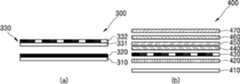
도 3의 (a)는 본 발명에 다른 실시예따른 색변환용 형광체층이 패터닝된 도광판을 포함하는 디스플레이 패널을 나타낸 모식도이고, (b)는 종래 OLED를 나타낸 모식도이다.FIG. 3 (a) is a schematic view illustrating a display panel including a light guide plate patterned with a color conversion phosphor layer according to another embodiment of the present invention, and FIG. 3 (b) is a schematic view showing a conventional OLED.
도 3에 나타난 바와 같이, 본 발명에 따른 색변환용 형광체층이 패터닝된 도광판을 포함하는 디스플레이 패널(300)은 하판 유리(310), TFT+청색광 LED 어레이(320), 유리 기판(331) 및 무기 형광체층(332)를 포함하는 도광판(330)으로 이루어진다. 반면, 종래 OLED(400)는 TFT/하판 유리(410), 전자 수송층(420), 유기 발광층(430), 정공 수송층(440), 버퍼층(450), 애노드/상판 유리(460) 및 편광판(470)으로 이루어진다.3, a
상기 TFT+청색광 LED 어레이(320)는 청색광 LED 광원과 박막트랜지스터(TFT)의 조합으로 이루어진 2차원의 LED로 배열된 층일 수 있다.The TFT +
따라서, 본 발명에 따른 색변환용 형광체층이 패터닝된 도광판을 포함하는 디스플레이 패널로 LED를 제조하는 경우에는 종래 OLED와 비교하여 다층구조를 획기적으로 감소시켜 백라이트유닛의 두께가 크게 감소하는 것을 알 수 있고, 유기소재가 아닌 순수한 무기소재로 제조되어 OLED 보다 내구성이 우수하면서 제조가 용이한 LED디스플레이를 제조할 수 있음을 알 수 있다.Therefore, when an LED is manufactured using a display panel including a light guide plate patterned with a color conversion phosphor layer according to the present invention, the thickness of the backlight unit is greatly reduced by drastically reducing the multilayer structure as compared with the conventional OLED And it is possible to manufacture an LED display which is manufactured from a pure inorganic material rather than an organic material and which is more durable than OLED and easy to manufacture.
따라서 본 발명의 실시예에 따른 색변환용 형광체층이 패터닝된 도광판 (120)은 종래 LCD의 도광판(220), 확산 필름(230) 및 반사층(210)을 일체화할 수 있어 LCD의 두께 및 공정 비용을 크게 감소시킬 수 있으며, 각 픽셀별 컬러를 제공함으로써 종래 LCD의 컬러 필터의 대체도 가능하고, 이를 통한 제품 내구성의 증대 및 생산단가의 저하를 유도할 수 있다.Therefore, the
지금까지 본 발명에 따른 색변환용 형광체층이 패터닝된 도광판 및 이를 포함하는 디스플레이 소자, 디스플레이 패널에 관한 구체적인 실시예에 관하여 설명하였으나, 본 발명의 범위에서 벗어나지 않는 한도 내에서는 여러 가지 실시 변형이 가능함은 자명하다.Although the embodiments of the light guide plate, the display device and the display panel including the color conversion phosphor layer according to the present invention have been described, various modifications are possible within the scope of the present invention. It is self-evident.
그러므로 본 발명의 범위에는 설명된 실시예에 국한되어 전해져서는 안 되며, 후술하는 특허청구범위뿐만 아니라 이 특허청구범위와 균등한 것들에 의해 정해져야 한다.Therefore, the scope of the present invention should not be limited to the above-described embodiments, but should be determined by the scope of the appended claims and equivalents thereof.
즉, 전술된 실시예는 모든 면에서 예시적인 것이며, 한정적인 것이 아닌 것으로 이해되어야 하며, 본 발명의 범위는 상세한 설명보다는 후술될 특허청구범위에 의하여 나타내어지며, 그 특허청구범위의 의미 및 범위 그리고 그 등가 개념으로부터 도출되는 모든 변경 또는 변형된 형태가 본 발명의 범위에 포함되는 것으로 해석되어야 한다.It is to be understood that the foregoing embodiments are illustrative and not restrictive in all respects and that the scope of the present invention is indicated by the appended claims rather than the foregoing description, It is intended that all changes and modifications derived from the equivalent concept be included within the scope of the present invention.
100 : 색변환용 형광체층이 패터닝된 도광판을 포함하는 LCD
110 : 반사층120 : 도광판
121 : 유리 기판122 : 청색광 LED 광원
123 : 무기 형광체층124 : 적색 및 녹색형광체 패턴 125 : 황색 및 녹색형광체 패턴 126 : 패터닝되지 않은 공간
130 : 프리즘 필름 140 : 제1 편광판
150 : TFT 층160 : 액정
170 : 상판 유리 180 : 제2 편광판
200 : 종래 LCD 210 : 반사층
220 : 도광판230 : 확산 필름
240 : 프리즘 필름 250 : 제1 편광판
260 : TFT 층270 : 액정
280 : 컬러필터290 : 제2 편광판
300 : 색변환용 형광체층이 패터닝된 도광판을 포함하는 디스플레이패널
310 : 하판 유리320 : TFT+청색 LED 어레이
330 : 유리 기판340 : 무기 형광체층
400 : 종래 OLED 410 : TFT/하판 유리
420 : 전자 수송층430 : 유기 발광층
440 : 정공 수송층450 : 버퍼층
460 : 애노드/상판 유리470 : 편광판100: LCD including a light guide plate patterned with a phosphor layer for color conversion
110: reflective layer 120: light guide plate
121: glass substrate 122: blue light LED light source
123: Inorganic phosphor layer 124: Red and green phosphor pattern 125: Yellow and green phosphor pattern 126: Unpatterned space
130: prism film 140: first polarizer plate
150: TFT layer 160: liquid crystal
170: upper plate glass 180: second polarizer plate
200: conventional LCD 210: reflective layer
220: light guide plate 230: diffusion film
240: prism film 250: first polarizer plate
260: TFT layer 270: liquid crystal
280: Color filter 290: Second polarizing plate
300: a display panel including a light guide plate patterned with a phosphor layer for color conversion
310: Lower plate glass 320: TFT + blue LED array
330: glass substrate 340: inorganic phosphor layer
400: conventional OLED 410: TFT / lower plate glass
420: electron transport layer 430: organic light emitting layer
440: hole transport layer 450: buffer layer
460: anode / top plate glass 470: polarizer
Claims (10)
Translated fromKorean상기 유리 기판의 일면에 패터닝되어 적색광 및 녹색광을 방출하는 무기 형광체층;
상기 유리 기판의 일측에 구비되는 청색광 LED 광원; 및
상기 유리 기판과 평행하도록 타면에 구비된 반사층을 포함하는 색변환용 형광체층이 패터닝된 도광판으로,
상기 유리 기판의 일면에는 상기 무기 형광체층내에 형광체가 함유되지 않은 무기층이 패터닝되거나 상기 무기 형광체층이 패터닝되지 않은 공간이 형성되어, 상기 청색광 LED 광원이 상기 무기 형광체층을 통과하여 그대로 방출되고,
상기 무기 형광체층은 형광체 분말, 글라스 프릿(frit) 및 유기 비히클을 혼합하여 페이스트로 제조한 후 스크린 프린팅하고 소성하여 형성되고,
상기 무기 형광체층은 SiO2, Al2O3, TiO2, ZrO2, Y2O3, WO3 으로 이루어진 군으로부터 선택되는 1종 이상의 산화물을 포함하고,
상기 무기 형광체층이 코팅된 도광판의 두께는 2 ㎛ 내지 75 ㎛인 것을 특징으로 하는, 색변환용 형광체층이 패터닝된 도광판.
A glass substrate;
An inorganic phosphor layer patterned on one surface of the glass substrate to emit red light and green light;
A blue light LED light source provided on one side of the glass substrate; And
And a reflective layer provided on the other surface so as to be parallel to the glass substrate, wherein the light-
Wherein a space is formed in one surface of the glass substrate such that an inorganic layer not containing a phosphor is patterned or the inorganic phosphor layer is not patterned in the inorganic phosphor layer so that the blue light LED light source passes through the inorganic phosphor layer,
The inorganic phosphor layer is formed by mixing a phosphor powder, a glass frit and an organic vehicle to prepare a paste, screen printing and firing,
Wherein the inorganic phosphor layer contains at least one oxide selected from the group consisting of SiO2 , Al2 O3 , TiO2 , ZrO2 , Y2 O3 and WO3 ,
Wherein a thickness of the light guide plate coated with the inorganic phosphor layer is 2 占 퐉 to 75 占 퐉.
상기 유리 기판은 알칼리실리케이트(alkali-silicate), 보로실리케이트(boro-silicate), 알루미노실리케이트(alumino-silicate), 리드실리케이드(lead-silicate) 및 포스페이트 실리케이트(phosphate silicate)로 이루어진 군으로부터 선택되는 1종의 규산계 유리 또는 옥시플루오라이드(oxyfluoride) 및 옥시니트라이드(oxynitride)로 이루어진 군으로부터 선택되는 1종의 산화물계 유리인 것을 특징으로 하는 색변환용 형광체층이 패터닝된 도광판.
The method according to claim 1,
Wherein the glass substrate is selected from the group consisting of alkali-silicate, boro-silicate, alumino-silicate, lead-silicate and phosphate silicate Wherein the color conversion phosphor layer is one kind of oxide-based glass selected from the group consisting of one kind of silica-based glass or oxyfluoride and oxynitride.
상기 형광체 분말은 황색 및 녹색형광체로써 이트륨 알루미늄 가넷(YAG) 및 테르븀 알루미늄 가넷(TAG)으로 이루어진 군으로부터 선택되는 1종의 알루미늄계 화합물과, 적색 및 녹색형광체로써 실리케이트 화합물, 나이트레이트계 화합물, 황화물계 화합물, 플루오라이드계 화합물, 옥시설파이드 (oxysulfide), 옥시나이트라이드 (oxynitride) 및 옥시플루오라이드(oxyfluoride)계 화합물로 이루어진 군으로부터 선택되는 1종 이상인 것을 특징으로 하는 색변환용 형광체층이 패터닝된 도광판.
The method according to claim 1,
The phosphor powder includes yellow and green phosphors, and includes at least one kind of aluminum compound selected from the group consisting of yttrium aluminum garnet (YAG) and terbium aluminum garnet (TAG), red and green phosphors, silicate compounds, nitrate compounds, sulfides Wherein the color conversion phosphor layer is at least one selected from the group consisting of a phosphorous compound, a fluorinated compound, an oxysulfide, an oxynitride, and an oxyfluoride compound, Light guide plate.
상기 글라스 프릿은 실리케이트계, 보레이트계 및 포스페이트계로 이루어진 군으로부터 선택되는 1종 이상의 유리 분말인 것을 특징으로 하는 색변환용 형광체층이 패터닝된 도광판.
The method according to claim 1,
Wherein the glass frit is at least one glass powder selected from the group consisting of silicates, borates and phosphates.
A display device comprising a light guide plate according to any one of claims 1, 2, 4, and 5.
A blue light LED light source is arranged two-dimensionally on one side of the light guide plate of any one of claims 1, 2, 4, and 5 to form a passive matrix (PM) or an active matrix (AM) Lt; RTI ID = 0.0 > 1, < / RTI >
Priority Applications (1)
| Application Number | Priority Date | Filing Date | Title |
|---|---|---|---|
| KR1020150186215AKR101806870B1 (en) | 2015-12-24 | 2015-12-24 | Light guide panel patterned color converting phosphor layer, display device and display panel comprising the same |
Applications Claiming Priority (1)
| Application Number | Priority Date | Filing Date | Title |
|---|---|---|---|
| KR1020150186215AKR101806870B1 (en) | 2015-12-24 | 2015-12-24 | Light guide panel patterned color converting phosphor layer, display device and display panel comprising the same |
Publications (2)
| Publication Number | Publication Date |
|---|---|
| KR20170076216A KR20170076216A (en) | 2017-07-04 |
| KR101806870B1true KR101806870B1 (en) | 2017-12-08 |
Family
ID=59357165
Family Applications (1)
| Application Number | Title | Priority Date | Filing Date |
|---|---|---|---|
| KR1020150186215AActiveKR101806870B1 (en) | 2015-12-24 | 2015-12-24 | Light guide panel patterned color converting phosphor layer, display device and display panel comprising the same |
Country Status (1)
| Country | Link |
|---|---|
| KR (1) | KR101806870B1 (en) |
Cited By (1)
| Publication number | Priority date | Publication date | Assignee | Title |
|---|---|---|---|---|
| DE102023116695A1 (en)* | 2023-06-26 | 2025-01-02 | HELLA GmbH & Co. KGaA | lighting device for a vehicle |
Families Citing this family (1)
| Publication number | Priority date | Publication date | Assignee | Title |
|---|---|---|---|---|
| CN116594224B (en)* | 2023-05-26 | 2024-06-18 | 惠科股份有限公司 | Backlight module and display device |
Citations (3)
| Publication number | Priority date | Publication date | Assignee | Title |
|---|---|---|---|---|
| JP2005353650A (en)* | 2004-06-08 | 2005-12-22 | Matsushita Electric Ind Co Ltd | LED light source and liquid crystal display device |
| JP2014207436A (en)* | 2013-03-18 | 2014-10-30 | 日本碍子株式会社 | Wavelength converter |
| JP2015520864A (en)* | 2012-04-20 | 2015-07-23 | メルク パテント ゲゼルシャフト ミット ベシュレンクテル ハフツングMerck Patent Gesellschaft mit beschraenkter Haftung | Electro-optic switching element and electro-optic display |
- 2015
- 2015-12-24KRKR1020150186215Apatent/KR101806870B1/enactiveActive
Patent Citations (3)
| Publication number | Priority date | Publication date | Assignee | Title |
|---|---|---|---|---|
| JP2005353650A (en)* | 2004-06-08 | 2005-12-22 | Matsushita Electric Ind Co Ltd | LED light source and liquid crystal display device |
| JP2015520864A (en)* | 2012-04-20 | 2015-07-23 | メルク パテント ゲゼルシャフト ミット ベシュレンクテル ハフツングMerck Patent Gesellschaft mit beschraenkter Haftung | Electro-optic switching element and electro-optic display |
| JP2014207436A (en)* | 2013-03-18 | 2014-10-30 | 日本碍子株式会社 | Wavelength converter |
Cited By (1)
| Publication number | Priority date | Publication date | Assignee | Title |
|---|---|---|---|---|
| DE102023116695A1 (en)* | 2023-06-26 | 2025-01-02 | HELLA GmbH & Co. KGaA | lighting device for a vehicle |
Also Published As
| Publication number | Publication date |
|---|---|
| KR20170076216A (en) | 2017-07-04 |
Similar Documents
| Publication | Publication Date | Title |
|---|---|---|
| JP7209051B2 (en) | display device | |
| TWI574055B (en) | Display panel | |
| CN105304684B (en) | Colour display device and preparation method thereof | |
| CN110333629B (en) | Partially driven light source device and image display device using the same | |
| TWI544620B (en) | Display panel | |
| US10134962B2 (en) | Quantum dot LED package structure | |
| CN101937911B (en) | Light-emitting diode packaging structure and backlight module | |
| CN105467670A (en) | Array substrate, display panel and liquid crystal display | |
| US20060284532A1 (en) | Color display unit | |
| TW201626009A (en) | Color conversion substrate, method of fabricating the same, and display device including the same | |
| CN103343943A (en) | Backlight module of display device and white light LED | |
| CN1881034A (en) | Color display unit | |
| CN204389849U (en) | A kind of quantum dot liquid crystal module and display device | |
| CN103869530A (en) | Liquid crystal displayer | |
| WO2015081692A1 (en) | Light guide plate, backlight source and liquid crystal display apparatus | |
| US10705278B2 (en) | Backlight unit and display device including the same | |
| EP3762471A1 (en) | Devices including green-emitting phosphors | |
| CN110534631A (en) | Wide color gamut backlight source for display of LED combined perovskite quantum dot glass ceramics | |
| CN203275836U (en) | Display device | |
| CN101261386A (en) | Liquid crystal display device and light emitting unit | |
| CN104849911B (en) | Display base plate, display panel and display device | |
| KR101806870B1 (en) | Light guide panel patterned color converting phosphor layer, display device and display panel comprising the same | |
| CN103117205A (en) | Display device, backlight module, field-emitting light source device of backlight module and manufacturing method of field-emitting light source device | |
| CN106483708A (en) | The control method of color membrane substrates, array base palte, display device and display device | |
| US20160377788A1 (en) | Backlight module and liquid crystal display device using the same |
Legal Events
| Date | Code | Title | Description |
|---|---|---|---|
| A201 | Request for examination | ||
| PA0109 | Patent application | Patent event code:PA01091R01D Comment text:Patent Application Patent event date:20151224 | |
| PA0201 | Request for examination | ||
| E902 | Notification of reason for refusal | ||
| PE0902 | Notice of grounds for rejection | Comment text:Notification of reason for refusal Patent event date:20170428 Patent event code:PE09021S01D | |
| PG1501 | Laying open of application | ||
| E701 | Decision to grant or registration of patent right | ||
| PE0701 | Decision of registration | Patent event code:PE07011S01D Comment text:Decision to Grant Registration Patent event date:20171122 | |
| GRNT | Written decision to grant | ||
| PR0701 | Registration of establishment | Comment text:Registration of Establishment Patent event date:20171204 Patent event code:PR07011E01D | |
| PR1002 | Payment of registration fee | Payment date:20171204 End annual number:3 Start annual number:1 | |
| PG1601 | Publication of registration | ||
| PR1001 | Payment of annual fee | Payment date:20201005 Start annual number:4 End annual number:4 | |
| PR1001 | Payment of annual fee | Payment date:20211102 Start annual number:5 End annual number:5 | |
| PR1001 | Payment of annual fee | Payment date:20220921 Start annual number:6 End annual number:6 | |
| PR1001 | Payment of annual fee | Payment date:20230921 Start annual number:7 End annual number:7 | |
| PR1001 | Payment of annual fee |