KR101801409B1 - Receiving means for mounting of wafers - Google Patents
Receiving means for mounting of wafersDownload PDFInfo
- Publication number
- KR101801409B1 KR101801409B1KR1020127009080AKR20127009080AKR101801409B1KR 101801409 B1KR101801409 B1KR 101801409B1KR 1020127009080 AKR1020127009080 AKR 1020127009080AKR 20127009080 AKR20127009080 AKR 20127009080AKR 101801409 B1KR101801409 B1KR 101801409B1
- Authority
- KR
- South Korea
- Prior art keywords
- wafer
- mounting surface
- mounting
- map
- aligning
- Prior art date
- Legal status (The legal status is an assumption and is not a legal conclusion. Google has not performed a legal analysis and makes no representation as to the accuracy of the status listed.)
- Active
Links
- 235000012431wafersNutrition0.000titleclaimsabstractdescription110
- 238000000034methodMethods0.000claimsabstractdescription17
- 238000011156evaluationMethods0.000claimsdescription4
- 238000012937correctionMethods0.000claimsdescription3
- 238000001514detection methodMethods0.000claimsdescription3
- 239000000463materialSubstances0.000claimsdescription3
- 230000009471actionEffects0.000claimsdescription2
- 238000010438heat treatmentMethods0.000description19
- 230000008901benefitEffects0.000description3
- 238000001816coolingMethods0.000description3
- 230000008569processEffects0.000description3
- 230000009466transformationEffects0.000description3
- 230000004913activationEffects0.000description2
- 238000004519manufacturing processMethods0.000description2
- 238000005259measurementMethods0.000description2
- 238000012360testing methodMethods0.000description2
- XLYOFNOQVPJJNP-UHFFFAOYSA-NwaterSubstancesOXLYOFNOQVPJJNP-UHFFFAOYSA-N0.000description2
- 230000008602contractionEffects0.000description1
- 230000001419dependent effectEffects0.000description1
- 230000000694effectsEffects0.000description1
- 239000000284extractSubstances0.000description1
- 238000000605extractionMethods0.000description1
- 238000001459lithographyMethods0.000description1
- 239000002184metalSubstances0.000description1
- 230000002093peripheral effectEffects0.000description1
- 230000003252repetitive effectEffects0.000description1
- 238000007789sealingMethods0.000description1
- 230000008961swellingEffects0.000description1
- 239000002470thermal conductorSubstances0.000description1
Images


Classifications
- H—ELECTRICITY
- H01—ELECTRIC ELEMENTS
- H01L—SEMICONDUCTOR DEVICES NOT COVERED BY CLASS H10
- H01L21/00—Processes or apparatus adapted for the manufacture or treatment of semiconductor or solid state devices or of parts thereof
- H01L21/67—Apparatus specially adapted for handling semiconductor or electric solid state devices during manufacture or treatment thereof; Apparatus specially adapted for handling wafers during manufacture or treatment of semiconductor or electric solid state devices or components ; Apparatus not specifically provided for elsewhere
- H01L21/68—Apparatus specially adapted for handling semiconductor or electric solid state devices during manufacture or treatment thereof; Apparatus specially adapted for handling wafers during manufacture or treatment of semiconductor or electric solid state devices or components ; Apparatus not specifically provided for elsewhere for positioning, orientation or alignment
- H—ELECTRICITY
- H01—ELECTRIC ELEMENTS
- H01L—SEMICONDUCTOR DEVICES NOT COVERED BY CLASS H10
- H01L21/00—Processes or apparatus adapted for the manufacture or treatment of semiconductor or solid state devices or of parts thereof
- H01L21/67—Apparatus specially adapted for handling semiconductor or electric solid state devices during manufacture or treatment thereof; Apparatus specially adapted for handling wafers during manufacture or treatment of semiconductor or electric solid state devices or components ; Apparatus not specifically provided for elsewhere
- H01L21/67005—Apparatus not specifically provided for elsewhere
- H01L21/67011—Apparatus for manufacture or treatment
- H01L21/67092—Apparatus for mechanical treatment
- H—ELECTRICITY
- H01—ELECTRIC ELEMENTS
- H01L—SEMICONDUCTOR DEVICES NOT COVERED BY CLASS H10
- H01L21/00—Processes or apparatus adapted for the manufacture or treatment of semiconductor or solid state devices or of parts thereof
- H01L21/67—Apparatus specially adapted for handling semiconductor or electric solid state devices during manufacture or treatment thereof; Apparatus specially adapted for handling wafers during manufacture or treatment of semiconductor or electric solid state devices or components ; Apparatus not specifically provided for elsewhere
- H01L21/67005—Apparatus not specifically provided for elsewhere
- H01L21/67242—Apparatus for monitoring, sorting or marking
- H01L21/67288—Monitoring of warpage, curvature, damage, defects or the like
- H—ELECTRICITY
- H01—ELECTRIC ELEMENTS
- H01L—SEMICONDUCTOR DEVICES NOT COVERED BY CLASS H10
- H01L21/00—Processes or apparatus adapted for the manufacture or treatment of semiconductor or solid state devices or of parts thereof
- H01L21/67—Apparatus specially adapted for handling semiconductor or electric solid state devices during manufacture or treatment thereof; Apparatus specially adapted for handling wafers during manufacture or treatment of semiconductor or electric solid state devices or components ; Apparatus not specifically provided for elsewhere
- H01L21/68—Apparatus specially adapted for handling semiconductor or electric solid state devices during manufacture or treatment thereof; Apparatus specially adapted for handling wafers during manufacture or treatment of semiconductor or electric solid state devices or components ; Apparatus not specifically provided for elsewhere for positioning, orientation or alignment
- H01L21/682—Mask-wafer alignment
- H—ELECTRICITY
- H01—ELECTRIC ELEMENTS
- H01L—SEMICONDUCTOR DEVICES NOT COVERED BY CLASS H10
- H01L21/00—Processes or apparatus adapted for the manufacture or treatment of semiconductor or solid state devices or of parts thereof
- H01L21/67—Apparatus specially adapted for handling semiconductor or electric solid state devices during manufacture or treatment thereof; Apparatus specially adapted for handling wafers during manufacture or treatment of semiconductor or electric solid state devices or components ; Apparatus not specifically provided for elsewhere
- H01L21/683—Apparatus specially adapted for handling semiconductor or electric solid state devices during manufacture or treatment thereof; Apparatus specially adapted for handling wafers during manufacture or treatment of semiconductor or electric solid state devices or components ; Apparatus not specifically provided for elsewhere for supporting or gripping
- H—ELECTRICITY
- H01—ELECTRIC ELEMENTS
- H01L—SEMICONDUCTOR DEVICES NOT COVERED BY CLASS H10
- H01L22/00—Testing or measuring during manufacture or treatment; Reliability measurements, i.e. testing of parts without further processing to modify the parts as such; Structural arrangements therefor
- H01L22/10—Measuring as part of the manufacturing process
- H01L22/12—Measuring as part of the manufacturing process for structural parameters, e.g. thickness, line width, refractive index, temperature, warp, bond strength, defects, optical inspection, electrical measurement of structural dimensions, metallurgic measurement of diffusions
- H—ELECTRICITY
- H01—ELECTRIC ELEMENTS
- H01L—SEMICONDUCTOR DEVICES NOT COVERED BY CLASS H10
- H01L2221/00—Processes or apparatus adapted for the manufacture or treatment of semiconductor or solid state devices or of parts thereof covered by H01L21/00
- H01L2221/67—Apparatus for handling semiconductor or electric solid state devices during manufacture or treatment thereof; Apparatus for handling wafers during manufacture or treatment of semiconductor or electric solid state devices or components; Apparatus not specifically provided for elsewhere
- H01L2221/683—Apparatus for handling semiconductor or electric solid state devices during manufacture or treatment thereof; Apparatus for handling wafers during manufacture or treatment of semiconductor or electric solid state devices or components; Apparatus not specifically provided for elsewhere for supporting or gripping
Landscapes
- Engineering & Computer Science (AREA)
- Manufacturing & Machinery (AREA)
- Computer Hardware Design (AREA)
- Microelectronics & Electronic Packaging (AREA)
- Power Engineering (AREA)
- Physics & Mathematics (AREA)
- Condensed Matter Physics & Semiconductors (AREA)
- General Physics & Mathematics (AREA)
- Container, Conveyance, Adherence, Positioning, Of Wafer (AREA)
Abstract
Translated fromKoreanDescription
Translated fromKorean본 발명은 청구항 제1항에 따르는 웨이퍼를 수용 및 장착하기 위한 수용 장치 및 청구항 제1항에 따르는 수용 장치를 사용하여 청구항 제8항 및 제9항에 따라서 제1 웨이퍼와 제2 웨이퍼를 정렬하기 위한 장치 및 방법에 관한 것이다.
The present invention relates to arranging a first wafer and a second wafer according to claims 8 and 9 using a receiving device for receiving and mounting wafers according to
이들 수용 수단 또는 샘플 홀더 또는 척은 별개의 유형으로 입수가능하고, 평평한 수용 표면 또는 장착은 수용 수단에 대해 결정적이어서 더 좁아지고 더 작은 구조물이 전체 웨이퍼 표면에 걸쳐서 더 넓어지고 더 넓은 웨이퍼 표면상에 정확히 정렬 및 결합될 수 있다. 이는 실제 결합 공정 이전에 분리가능한 상호연결부에 의해 웨이퍼를 서로 결합하는 소위 사전결합 단계가 수행될 때 특히 중요하다. 서로에 대한 웨이퍼의 고 정렬 정확도는 정렬 정확도 또는 특히 2 μm 미만의 뒤틀림 값이 하나의 웨이퍼 또는 웨이퍼 양자 모두에 대해 구현되자마자 특히 중요하다. 정렬 마크의 주변에서, 지시된 수용 수단 및 소위 정렬기, 특히 결합 정렬기(bond aligner)로 불리는 정렬을 위한 장치에 특히 적합하게 적용된다. 정렬 마크로부터의 거리가 증가됨에 따라, 제어되고 완벽한 정렬이 구현되며, 정렬 정확도 또는 특히 2 μm보다 높고, 특히 1 μm 및 심지어 더 바람직하게는 0.25 μm보다 높은 뒤틀림 값이 구현될 수 없다.
These receiving means or sample holders or chucks are available in separate types and the flat receiving surface or mounting is crucial to the receiving means so that it becomes narrower and smaller structures are wider over the entire wafer surface and on the wider wafer surface Can be accurately aligned and combined. This is particularly important when a so-called pre-bonding step of bonding the wafers to each other by a separable interconnect before the actual bonding process is performed. The high alignment accuracy of the wafers to each other is particularly important as soon as the alignment accuracy, or especially a distortion value of less than 2 μm, is realized for both wafers or wafers. In the periphery of the alignment marks, it is particularly suitable for the apparatus for alignment indicated by the indicated receiving means and the so-called aligner, in particular a bond aligner. As the distance from the alignment mark is increased, a controlled and perfect alignment is realized, and no alignment accuracy or especially a distortion value higher than 2 [mu] m, especially 1 [mu] m and even more preferably 0.25 [mu] m, can be realized.
본 발명의 목적은 더욱 정확한 정렬이 이에 따라 구현될 수 있도록 일반적인 수용 수단을 향상시키는 데 있다.
It is an object of the present invention to improve general acceptance measures so that more accurate alignment can be implemented accordingly.
이 목적은 청구항 제1항, 제8항 및 제9항의 특징에 따라 구현된다. 본 발명의 선호되는 이점이 종속항에 제시된다. 명세서, 청구항 및/또는 도면에 제시된 둘 이상의 특징의 모든 조합이 본 발명의 범위 내에 있다. 주어진 값의 범위에서, 제시된 한계점 내의 값들은 또한 경계값으로서 개시되고, 임의의 조합으로 청구될 것이다.This object is achieved according to the features of
본 발명은 유럽 특허 출원 제EP 09012023호 및 제EP 10 015 569호에 따르는 출원인의 결과물을 기초로 하고, 전자의 출원의 경우, 전체 표면, 특히 웨이퍼의 위치 지도로서 각각의 웨이퍼의 표면상에서 구조물의 위치의 감지가 가능하다. 후자의 출원은 제1 웨이퍼가 제2 웨이퍼에 결합될 때, 제2 웨이퍼에 대한 제1 웨이퍼의 뒤틀림 및/또는 변형으로 인해 발생되는 국부적인 정렬 오차를 측정하기 위한 장치에 관한 것으로,The present invention is based on the results of the applicants according to the European patent application EP 09012023 and
-제1 웨이퍼의 제1 접촉 표면을 따르는 변형 값의 제1 변형 지도 및/또는A first deformation map of the deformation value along the first contact surface of the first wafer and /
-제2 접촉 표면을 따르는 변형 값의 제2 변형 지도 및A second deformation map of deformation values along the second contact surface and
-국부적인 정렬 오차가 측정될 수 있는 제1 및/또는 제2 변형 지도를 평가하기 위한 평가 수단을 포함한다.And evaluation means for evaluating the first and / or second variant maps from which local alignment errors can be measured.
본 발명의 기본적인 사상은 서로 독립적인 몇몇의 능동 제어 요소로 구성되는 수용 수단을 제공하는 것이며, 이에 따라 수용 수단의 장착 표면은 특히 형태 및/또는 온도에 있어서 영향을 받을 수 있다. 여기서, 능동 제어 요소는 위치 지도 및/또는 변형 지도에 의해 알려진 국부적인 정렬 오차 또는 국부적인 뒤틀림이 상쇄되거나 또는 대부분이 최소화 또는 감소되도록 대응하는 활성화에 의해 사용된다. 여기서 국부적인 뒤틀림이 제거될 뿐만 아니라 전체적으로 이의 외측 치수에서 국부적인 뒤틀림으로부터 야기되는 웨이퍼의 육안으로 보이는 뒤틀림 또는 연신이 동시에 최소화 또는 교정된다.The basic idea of the present invention is to provide a receiving means consisting of several independent active control elements so that the mounting surface of the receiving means can be particularly affected by the shape and / or the temperature. Here, the active control element is used by a corresponding activation such that the local alignment error or local distortion known by the position map and / or the transformation map is canceled or most of it is minimized or reduced. Here, not only the local distortion is eliminated, but also the visible distortion or stretching of the wafer caused by the local distortion in its overall outside dimension is minimized or corrected at the same time.
따라서, 본 발명에 청구된 바와 같이, 특히 위치 지도, 변형 지도 및/또는 응력 지도 및 개시된 정렬 오차의 원 위치로의 교정에 관한 전술된 본 발명과 조합하여, 웨이퍼의 접촉-형성 및 결합 동안에 능동, 특히 웨이퍼의 뒤틀림에 대한 국부적인 작용에 의해 여전히 더 우수한 정렬 결과를 구현할 수 있다.Thus, as claimed in the present invention, in particular in combination with positional maps, deformed maps and / or stress maps and the previously described inventions relating to the correction of the disclosed alignment errors to their original positions, Can still achieve better alignment results, especially by local action on the warp of the wafer.
본 발명의 일 선호되는 실시예에 따라서, 장착 표면의 온도는 교정 수단에 국부적으로 영향을 받을 수 있다. 장착 표면의 국부적인 온도 증가에 따라 이 위치에서 장착 표면에 보유되는 웨이퍼의 국부적인 팽창이 야기된다. 온도 구배가 더 커질수록 이 위치에서 웨이퍼는 더욱더 팽창한다. 위치 지도 및/또는 변형 지도의 데이터, 특히 정렬 오차의 벡터 평가를 기준으로, 특히 위치 지도 및/또는 변형 지도의 각각의 위치에 대해, 제어된 방식으로 이들을 상쇄시키거나 또는 국부적인 웨이퍼 뒤틀림에 대해 작용할 수 있다.According to one preferred embodiment of the invention, the temperature of the mounting surface can be locally influenced by the calibration means. The local temperature increase of the mounting surface causes a local expansion of the wafer held at the mounting surface at this location. The larger the temperature gradient, the more the wafer expands at this location. For each position of the position map and / or deformation map, based on the vector evaluation of the data, in particular of the alignment error, in particular of the position map and / or the deformation map, it is possible to offset them in a controlled manner or to compensate them for local wafer distortion Lt; / RTI >
이에 따라 벡터 평가는 뒤틀림 벡터를 갖는 벡터장으로서 형성되고, 특히, 이 벡터장은 후술된 본 발명의 2가지의 버전들 중 하나의 버전에 의해 결정된다.The vector evaluation is thus formed as a vector field with a warping vector, and in particular, this vector field is determined by a version of one of the two versions of the invention described below.
제1 버전은 2개의 웨이퍼 중 단지 하나의 웨이퍼만이 구조화되는 응용에 관한 것이다. 이 경우에, 본 발명에 청구된 바와 같이, 구조물의 편차가 감지되고, 특히 원하는 형태로부터 기하학적 형태의 편차가 감지된다. 이 경우에, 통상적으로 직사각형인 정상적으로 예상된 형태로부터 노출장, 특히 스텝 앤드 리피트 노출 장치(step & repeat exposure device)의 노출장의 형태의 편차가 특히 관심이다. 이들 편차, 특히 이들 편차를 나타내는 벡터장은 EP 09012023에 따르는 노출장에 대응되는 개개의 정렬 마크의 위치 지도의 감지를 기준으로 수행된다. 대안적으로, 이 벡터장은 또한 EP 10 015 569.6에 의해 획득되는 응력 지도 및/또는 변형 지도를 기준으로 결정될 수 있다. 대안적으로, 그러나 이 벡터장은 본 발명에서 청구된 바와 같이 또한 임의의 그 외의 다른 적합한 측정 수단일 수 있으며, 판독될 수 있다. 특히 특정 테스트 마스크 및/또는 특정 테스트 루틴에 따라 이들 데이터를 획득하기 위해 작동되는 스텝 앤드 리피트 리소그래피 시스템(step & repeat lithography system)은 이 특정을 위해 적합할 수 있다.The first version concerns applications in which only one of the two wafers is structured. In this case, as claimed in the present invention, the deviation of the structure is sensed, and in particular the deviation of the geometry from the desired shape is sensed. In this case, the variation of the shape of the exposure field, especially the exposure field of the step & repeat exposure device, from a normally expected form, which is usually rectangular, is of particular interest. These deviations, in particular the vector field representing these deviations, are carried out on the basis of the detection of the position map of the individual alignment marks corresponding to the exposure field according to EP 09012023. Alternatively, this vector field can also be determined on the basis of a stress map and / or a transformation map obtained by
제2 버전은 2개의 웨이퍼가 구조화되는 응용에 관한 것이다. 이 경우에, 본 발명에서 청구된 바와 같이 정렬 편차의 벡터장은 위치 지도, 특히 EP 09012023에 따르는 제1 및 제2 위치 지도의 모든 위치에 대해 연산된다. 이 벡터장은 특히 EP 10 015 569.6에서의 물질에 따르는 기술적 및/또는 경제적 기준에 따라 이상적인 것으로 고려되는 정렬 위치에 대해 결정되어진다.The second version relates to an application in which two wafers are structured. In this case, the vector field of the alignment deviation as claimed in the present invention is calculated for all positions of the first and second position maps according to the position map, in particular according to EP 09012023. This vector field is determined, in particular, for alignment positions considered ideal according to the technical and / or economic criteria according to the material in
본 발명의 또 다른 선호되는 실시예에서, 장착 표면의 변형은 교정 수단, 특히 장착 표면의 일 후방에 개별적으로 작용할 수 있는 압전요소의 배열에 국부적으로 영향을 받을 수 있다. 연신 또는 수축, 이에 따라서 음의 연신에 의해, 또한 웨이퍼는 이에 따라 변형되고, 특히 웨이퍼 상의 장착 표면으로부터 작용하는 장착력에 의해 연신 또는 수축되고, 이에 따라 이 방식으로 웨이퍼는 이 웨이퍼에 대해 결정되는 변형 지도의 값을 기준으로 대응하는 제어 수단에 의해 제어된 방식으로 영향을 받을 수 있다. 장착 표면의 형태가 교정 수단, 특히 하나의 Z 방향으로 바람직하게는 기게적 작용에 의해 국부적으로 영향을 받을 수 있는 정도까지 장착 표면 상에서 웨이퍼의 뒤틀림을 상쇄하기 위한 또 다른 가능성이 있다. 또한 여기서 이는 교정 수단의 제어가 위치 지도 및/또는 변형 지도의 값을 기준으로 교정 수단의 이에 대응하는 국부적인 제어를 수행하는 제어 수단에 의해 구현되는데 적용된다.In another preferred embodiment of the present invention, the deformation of the mounting surface can be locally influenced by the calibration means, in particular the arrangement of the piezoelectric elements, which can act individually on one side of the mounting surface. The stretching or contraction, and thus the negative stretching, also causes the wafer to deform accordingly, in particular to stretch or retract by its mounting force acting from the mounting surface on the wafer, and in this way the wafer is determined for this wafer Can be influenced in a manner controlled by the corresponding control means on the basis of the value of the deformation map. There is another possibility to offset the warping of the wafer on the mounting surface to such an extent that the shape of the mounting surface can be locally influenced by the calibration means, especially in one Z direction, preferably by cogging. It is also applied here that the control of the calibration means is implemented by a control means which performs a local control corresponding to the calibration means on the basis of the value of the position map and / or the transformation map.
특히, 제어 수단은 대응하는 루틴을 실시/연산하기 위한 소프트웨어를 포함한다.In particular, the control means comprises software for implementing / computing a corresponding routine.
본 발명의 또 다른 선호되는 실시예에 따라서, 장착 표면은 특히 유압식 및/또는 공압식으로 교정 수단에 의해 장착 표면의 후방으로부터의 압력에 국부적으로 노출될 수 있다. 이 방식으로 장착 표면의 형태에 영향을 미칠 수 있어서 전술된 효과가 유발된다. 게다가, 전술된 제어 수단을 이용하여 제어가 구현된다.According to another preferred embodiment of the present invention, the mounting surface can be locally exposed to pressure from the rear of the mounting surface by means of calibration, in particular hydraulic and / or pneumatic. In this way, the shape of the mounting surface can be influenced and the above-mentioned effect is caused. In addition, control is implemented using the control means described above.
바람직하게는, 교정 수단은 특히 장착 표면 내에 일체구성된, 바람직하게는 이 내에 매립된 수용 수단 내의 복수의 능동 제어 요소로서 제공된다. 따라서, 수용 수단의 수용기는 공지된 수용 수단 내에서와 같이 일체형으로 형성될 수 있다.Preferably, the calibration means is provided as a plurality of active control elements, particularly in a receiving means integral with, preferably embedded within, the mounting surface. Thus, the receptors of the receiving means can be formed integrally as in known receiving means.
여기서, 각각의 제어 요소 또는 제어 요소의 그룹이 개별적으로 활성화될 수 있는 것이 특히 선호된다. 따라서, 국부적인 활성화는 작은 적출부(extract), 특히 웨이퍼의 절반보다 더 작은 적출부, 바람직하게는 웨이퍼의 1/4 보다 작은, 바람직하게는 웨이퍼의 1/8보다 작은, 심지어 더 바람직하게는 웨이퍼의 1/16 보다 작은 적출부가 교정 수단에 의해 국부적으로 활성화될 수 있음을 의미한다. 특히, 교정 수단은 적어도 하나의 제어 요소를 포함하는 자체 구조물에 의해 점유된 웨이퍼의 각각의 영역에 작용할 수 있다.Here it is particularly preferred that each control element or group of control elements can be activated individually. Thus, local activation is advantageous for small extracts, especially smaller than half of the wafers, preferably smaller than 1/4 of the wafer, preferably smaller than 1/8 of the wafer, It means that the extraction part smaller than 1/16 of the wafer can be locally activated by the calibration means. In particular, the calibration means may act on each region of the wafer occupied by its own structure comprising at least one control element.
본 발명에 청구된 장치는 바람직하게는 모든 제어 공정에 대해 신뢰성이 있는 중심 제어 유닛 내에서의 전술된 제어 수단을 포함한다. 그러나, 본 발명에서 청구된 바와 같이 특히 전체 장치의 모듈로서 수용 수단 내에 제어 수단을 제공할 수 있다.The apparatus claimed in the present invention preferably includes the aforementioned control means within a central control unit that is reliable for all control processes. However, as claimed in the present invention, it is particularly possible to provide control means within the receiving means as a module of the entire apparatus.
본 발명에 청구된 바와 같이, 방법은 정렬 이후 제1 및/또는 제2 웨이퍼의 위치 지도 및/또는 변형 지도의 특히 반복적인 획득에 의해 추가로 향상될 수 있다. 따라서, 본 발명에 청구된 바와 같이 정렬 완료 이후 정렬 성공의 체크가 있을 수 있다. 따라서, 예를 들어, 본 발명에 청구된 바와 같이 이를 정렬하거나 또는 이를 처리하기 위하여 지나치게 큰 정렬 오류에 따른 웨이퍼 쌍을 제거할 필요가 있을 수 있다. 동시에, 수득된 데이터는 특히 제어 수단에 의해 장치의 자가-교정을 위해 사용될 수 있다.As claimed in the present invention, the method may be further enhanced by a particularly repetitive acquisition of position maps and / or deformation maps of the first and / or second wafers after alignment. Thus, there may be a check of alignment success after alignment completion as claimed in the present invention. Thus, for example, it may be necessary to remove a wafer pair due to an oversized misalignment in order to align it or to process it, as claimed in the present invention. At the same time, the data obtained can be used for self-calibration of the device, in particular by means of control means.
유럽 특허 출원 EP 09012023.9호 및/또는 유럽 특허 출원 EP 10 015 569.6호에 개시된 발명은 본 발명의 실시예와 동시에 개시되는 것으로 고려될 것이다.The invention disclosed in European patent application EP 09012023.9 and / or European
본 발명의 그 외의 다른 이점, 특징 및 세부사항은 도면을 이용하여 선호되는 예시적인 실시예의 하기 기술내용으로부터 명확해질 것이다.
Other advantages, features, and details of the present invention will become apparent from the following description of exemplary embodiments which are preferred with reference to the drawings.
도 1a는 제1 실시예에서 본 발명에 청구된 바와 같이 수용 수단의 평면도.
도 1b는 도 1a의 절단선 A-A에 따르는 수용 수단의 단면도.
도 2a는 제2 실시예에서 본 발명에 청구된 바와 같이 수용 수단의 평면도.
도 2b는 도 2a의 절단선 B-B에 따르는 수용 수단의 단면도.
도 3a는 제3 실시예에서 본 발명에 청구된 바와 같이 수용 수단의 평면도.
도 3b는 도 3a의 절단선 C-C에 따르는 수용 수단의 단면도.
도 4a는 제4 실시예에서 본 발명에 청구된 바와 같이 수용 수단의 평면도.
도 4b는 도 4a의 절단선 D-D에 따르는 수용 수단의 단면도.BRIEF DESCRIPTION OF THE DRAWINGS Fig. 1A is a plan view of a receiving means as claimed in the present invention in a first embodiment; Fig.
1B is a sectional view of the receiving means along the cutting line AA in FIG.
Figure 2a is a plan view of a receiving means as claimed in the present invention in a second embodiment;
FIG. 2B is a cross-sectional view of the receiving means according to the cutting line BB in FIG. 2A; FIG.
Figure 3a is a plan view of a receiving means as claimed in the present invention in a third embodiment;
Figure 3b is a cross-sectional view of the receiving means according to the cutting line CC of Figure 3a.
Figure 4a is a top view of the receiving means as claimed in the present invention in a fourth embodiment.
Figure 4b is a cross-sectional view of the receiving means according to the cutting line DD of Figure 4a.
동일한 부품/특징부 및 동일한 기능을 갖는 부품/특징부는 도면에서 동일한 도면부호로 표시된다.The same parts / features and parts / features having the same functions are denoted by the same reference numerals in the drawings.
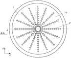
모두 4가지의 실시예는 평평한, 바람직하게는 원형의 링-형태의 플레이트와 같이, 웨이퍼의 수용 및 장착을 위한 평평한 장착 표면(1o)이 제공되는 일체형 수용기(monolithic receiver, 1)를 예시한다. 수용기는 외측 주연부 상에 링-형태의 숄더(ring-shaped shoulder, 1a)를 갖는다.All four embodiments illustrate a
장착 표면(1o)은 웨이퍼를 수용하기 위한 수용 평면을 형성하고, 이 평면은 X 및 Y 방향으로 신장된다. 물에 작용하는 장착력이 향하는 Z 방향은 이들에 대해 수직하게 이어진다. 웨이퍼의 장착은 음압을 개구(2)에 인가함으로써 장착 표면상에 웨이퍼를 고정시키기 위해 장착 표면(1o)에 걸쳐 균일하게 분포되어 배열되는 개구(2)를 통해 수행된다. 개구(2)의 개수가 더 많아지고 개구(2)의 직경이 더 작아질수록, 웨이퍼를 장착하기 위한 개구(2) 상에 가해지는 음압이 더 작아져서 개구(2) 상에서 웨이퍼의 뒤틀림이 야기된다.The mounting surface 1o forms a receiving plane for receiving a wafer, which extends in the X and Y directions. The Z direction to which the mounting force acting on the water is directed is perpendicular to these. The mounting of the wafers is carried out through the
개구(2) 상의 음압은 장착 표면(1o)의 후방 측면에 배치된 내측 공간(1i)에 대해 음압을 인가하고 도시되지 않은 진공 수단에 의해 인가된다. 게다가, 내측 공간(1i)은 수용기(1)의 주변 벽(1w)에 의해 접하고, 주변에 대해 밀봉된다. 개구(2)는 내측 공간(1i)까지 장착 표면(1o)으로부터 연장되고, 따라서, 내측 공간(1i) 내에서의 음압에 대해 균일하게 노출될 수 있다.The negative pressure on the
게다가, 내측 공간(1i)은 도시되지 않은 내측 공간(1i)의 하부와 장착 표면(1o)에 마주보게 위치된 후방(1r)에 의해 접하고, 후방(1r)은 개구(2)에 의해 침투된다.In addition, the
후방(1r)에서, 능동 제어 요소는 복수의 가열/냉각 요소, 특히 전적으로는 가열 요소(3)이다. 가열 요소(3)는 개별적으로 또는 무리를 이루어 각각 작동되고, 도시되지 않은 제어 수단에 의해 제어된다. 가열 요소(3) 중 하나의 가열 요소가 가열될 때, 장착 표면(1o)의 국부적인 섹션이 매우 우수한 열 전도체, 특히 수용기의 금속을 갖는 재료에 의해 가열된다. 이에 따라 이 영역에서 장착 표면(1o) 상에 배치된 웨이퍼가 국부적으로 팽창된다. 따라서, 수용 수단상에 정렬되어 보유되는 웨이퍼의 경우, 가능한 뒤틀림/변형의 알려진 위치에 따라 웨이퍼의 변형은 국부적인 뒤틀림을 교정하기 위해 개개의 또는 몇몇의 가열 요소(3)를 스위칭함으로써 제어 방식으로 수행될 수 있다. 특히, 복수의 국부적인 교정의 경우, 이는 또한 특히, X 및/또는 Y 방향으로 웨이퍼의 직경의 변화, 광범위한 뒤틀림의 광범위한 교정을 야기한다.At the rear 1r, the active control element is a plurality of heating / cooling elements, in
가열 및/또는 냉각 요소에 의한 웨이퍼 상에서의 뒤틀림에 영향을 미치는 일 특정 이점은 특히, 장착 표면의 변형 없이 및/또는 수직 방향 또는 Z 방향으로 웨이퍼의 변형 없이 최소의 변형으로 이를 구현할 수 있는 가능성에 있다. 이에 따라, 최소의 변형은 5 μm 미만, 선호적으로는 2 μm 미만, 바람직하게는 1 μm 미만 및 심지어 더 바람직하게는 0.5 μm 미만의 지지 표면에 대한 Z 방향 또는 수직 방향으로 장착 표면, 특히 웨이퍼의 변형이도록 고려되어야 한다.One particular advantage that affects warping on the wafer by heating and / or cooling elements is the ability to implement this with minimal deformation, especially without deformation of the mounting surface and / or without deformation of the wafer in the vertical or Z direction have. Thus, the minimum deformation is achieved in the Z direction or in the vertical direction relative to the support surface of less than 5 μm, preferably less than 2 μm, preferably less than 1 μm and even more preferably less than 0.5 μm, As shown in Fig.
이는 반-데르-발스 결합(van-der-Waals bond)을 기반으로 하는, 예를 들어, 사전결합과 같은 사전결합 상호연결부를 제조하는데 특히 선호된다. 여기서 장착 표면, 특히 웨이퍼가 평평하게 유지될 수 있음에 따라, 이들 사전결합 단계에서 통상적인 결합 웨이브(bond wave)는 비편평함(unevenness)으로 인해 이의 전파에 영향을 미치지 않는다. 따라서, 비결합 부위(소위 공극)가 잔류하는 위험성이 상당히 감소된다. 본 발명에서 청구된 바와 같이, 이들 사전결합 상호연결부를 제조하기 위해, 전체 웨이퍼 표면에 대한 5 μm 미만, 바람직하게는 2 μm 미만, 바람직하게는 1 μm 및 심지어 더욱 바람직하게는 0.5 μm 미만의 장착 표면의 편평함이 선호된다. 이들 편평함 값은 웨이퍼와 접촉하는 장착 표면의 일부분 내의 가장 높은 지점과 가장 낮은 지점 사이의 거리로서 정의된다.This is particularly preferred for manufacturing pre-bonded interconnects, such as pre-bonds, for example, based on van-der-Waals bonds. Here, as the mounting surface, especially the wafer, can be kept flat, the bond wave that is typical in these pre-bonding steps does not affect its propagation due to the unevenness. Thus, the risk of remaining non-bonding sites (so-called voids) is considerably reduced. As claimed in the present invention, for the fabrication of these pre-bonded interconnects, a mounting of less than 5 μm, preferably less than 2 μm, preferably less than 1 μm and even more preferably less than 0.5 μm on the entire wafer surface Flatness of the surface is preferred. These flatness values are defined as the distance between the highest point and the lowest point within a portion of the mounting surface in contact with the wafer.
가열 요소(3)는 수용 수단 내에 바람직하게는 장착 표면(1o) 아래에 균일하게 분포된다. 바람직하게는, 10개 초과의 가열 요소(3), 특히 50개 초과의 가열 요소(3), 바람직하게는 100개 초과의 가열 요소(3), 심지어 더 바람직하게는 500개 초과의 가열 요소(3)가 있다. 이들 가열 요소는 웨이퍼 상에서 국부적인 작동이 가능하고 장착 표면에서 개별적으로 작동될 수 있는 영역을 형성한다. 바람직하게는, 장착 표면의 개개의 영역은 적합한 수단을 이용하여 서로 단열된다. 특히, 영역은 개개의 세그먼트의 균일하고 제한된 배열을 허용하는 형태로 형성된다. 바람직하게는, 삼각형, 사각형 또는 6각형과 같은 세그먼트들의 배치가 이 목적에 대해 적합할 수 있다.The
특히, 페티에(Peltier) 요소가 가열 요소로서 적합할 수 있다.In particular, a Peltier element may be suitable as a heating element.
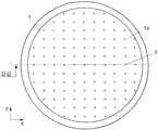
도 2a 및 도 2b에 도시된 제2 실시예에서, 가열 요소(3)는 도시되지 않고, 이들 대신에 또는 이와 조합하여 바람직하게는 장착 표면(1o)에 대한 거리보다 후방(1r)에 대하여 더 큰 거리로 장착 표면(1o) 상에 압전요소(4)가 제공된다.In the second embodiment shown in Figs. 2A and 2B, the
이 방식으로, 장착 표면(1o) 상에서 제어 작동이 가능하다. 압전요소(4)는 작동 시에 나노미터 내지 미크론 범위의 변형을 야기할 수 있다.In this manner, control operation is possible on the mounting surface 1o.
압전요소(4)의 개수는 전술된 가열 요소(3)의 개수와 일치될 수 있으며, 두 실시예의 조합이 본 명세서에서 청구된 것으로 인식될 수 있다.The number of
도 3a 및 도 3b에 도시된 본 발명의 제3 실시예에서, 가열 요소(3) 및/또는 압전요소(4) 대신에 또는 이와 조합하여 특히, 뾰족한 핀 단부(5e)를 포함하는, 장착 표면(1o) 상에서 말단을 이루는 핀(5)이 제공된다. 핀(5)의 초기 위치에서, 핀 단부(5e)는 장착 표면(1o)과 동일한 높이이다. 왜곡 지도 또는 변형 지도(strain map)의 정보와 같이 특정 핀(5)의 영역에서 웨이퍼의 국부적인 뒤틀림이 있을 정도로, 제어 수단은 웨이퍼의 방향, Z 방향으로 이동하는 핀 단부(5e) 또는 핀(5)에 의해 개개 또는 몇몇의 핀(5)을 작동시킴으로써 웨이퍼 상에 국부적으로 작용할 수 있다. 따라서, 핀 단부(5e)는 이 지점에서 웨이퍼의 국부적인 부풀림 또는 편향을 위해 제공되는 압축력에 대해 웨이퍼를 국부적으로 노출시킨다. 핀(5)은 후방(1r)까지 장착 표면으로부터 연장되는 가이드 개구(7) 내에서 전체적으로 슬라이드하도록 안내될 수 있다. 대안적으로, 단지 핀 단부(5e)만이 핀(5) 내에서 이동할 수 있으며, 핀(5) 또는 핀의 하측 섹션은 가이드 개구(7)에 대해 고정된다. 이 방식으로, 핀(5) 또는 핀의 특정 밀봉이 내측 공간(1r)에 대해 보장된다.In a third embodiment of the invention shown in Figures 3a and 3b, a mounting
핀(5)의 개수는 가열 요소(3) 또는 압전요소(4)의 개수와 일치되며, 여기서 하나 이상의 전술된 실시예의 조합이 가능하다.The number of
도 4에 도시된 실시예에서, 수용기(1)는 도 4b에 도시된 이의 상측 벽(6o)과 함께 장착 표면(1o)을 형성하는 복수의 압력 챔버(6)를 갖는다. 압력 챔버(6)는 내측 공간(1i)을 통해 연장되고, 이에 대해 밀봉된다. 각각의 압력 챔버(6) 또는 압력 챔버(6)의 그룹은 개별적으로 압축되고, 전술된 제어 수단에 의해 제어될 수 있다. 압력이 인가될 때, 압력 챔버(6)는 압력을 견디도록 적어도 상측 벽(6o) 상에 형성되며, 이에 따라 압력 챔버(6)의 그 외의 다른 경계 벽보다 더 얇아지고 및/또는 유연해진다. 개구(2)는 내측 공간(1i)에 연결된다.In the embodiment shown in Figure 4, the
본 발명에 청구된 바와 같이, 장착 표면(1o)의 최소의 국부적인 편향이 최대 3 μm, 특히, 최대 1 μm, 바람직하게는 최대 100 μm 정도로 전술된 교정 수단(3, 4, 5)에 의해 수행된다.By means of the calibration means 3, 4, 5 described above, the minimum local deflection of the mounting surface 1o is at most 3 μm, in particular at most 1 μm, preferably at most 100 μm, .
전술된 하나 이상의 실시예에 따라 국부적인 뒤틀림을 상쇄시키기 위해, 전술된 바와 같이 제어 수단은 어디에, 어느 정도까지, 또는 웨이퍼 내에서의 뒤틀림이 있는 방향을 인지할 필요가 있다. 그 뒤, 단지 제어 작동 또는 뒤틀림의 상쇄 및 교정만이 가능하다. 각각의 웨이퍼의 변형 지도는 EP 10 015 569.6에 따르는 대응하는 측정 수단으로 측정되고, 웨이퍼에 걸쳐서 분포되는 스트레인 벡터의 형태의 정보를 산출한다. 대응하는 제어 데이터는 웨이퍼의 위치 맵에 의해 지시되는 위치에서 웨이퍼의 변형 지도에 따라 각각의 웨이퍼에 대해 개별적인 제어를 수행하기 위하여 제어 유닛 내에 기록되고 특히, 경험적으로 측정된다. 교정은 웨이퍼의 정렬 동안에 이 방식으로 자동적으로 수행될 수 있다. 능동 제어 요소(3, 4, 5, 6)는 도면에 실측으로 도시되지 않고 또한 상이한 크기와 형태를 가질 수 있다.
To counteract localized warping in accordance with one or more of the above-described embodiments, the control means need to be aware of where, to what extent, or where there is warping in the wafer as described above. Thereafter, only control operations or distortion can be canceled and corrected. The deformation maps of each wafer are measured with corresponding measurement means in accordance with
1수용기
1a링-형태의 숄더
1i내측 공간
1o장착 표면
1w주변 벽
2개구
3 가열/냉각 요소
4압전 요소
5핀
5e핀 단부
6압력 챔버
6o상측 벽
7가이드 개구1 receptor
1a ring-shaped shoulder
1i inner space
1o mounting surface
1w surrounding wall
2 aperture
3 Heating / Cooling Element
4 Piezoelectric element
5 pin
5e pin end
6 Pressure chamber
6o upper wall
7 guide opening
Claims (15)
Translated fromKorean제1 웨이퍼의 제1 변형 지도 또는 제2 웨이퍼의 제2 변형 지도를 감지하고, 제1 또는 제2 변형 지도를 평가 수단에 의해 평가하며, 국부적 정렬 오차를 측정하는 단계,
웨이퍼의 수용 및 장착을 위한 수용 수단 상에 제1웨이퍼와 제2웨이퍼 중 하나 이상의 웨이퍼를 수용하는 단계 - 상기 수용 수단은 a) 장착 표면(1o), b) 장착 표면(1o) 상에 웨이퍼를 장착하기 위한 장착 수단 및 c) 웨이퍼의 국부적인 또는 전체적인 뒤틀림의 능동적인 국부적 교정을 위한 교정 수단(3, 4, 5, 6)을 포함함 - , 및
교정 수단에 의해 웨이퍼를 교정하고, 위치 지도 또는 변형 지도를 고려하여 제1웨이퍼와 제2웨이퍼를 정렬하는 단계를 포함하는 제1 웨이퍼와 제2 웨이퍼를 정렬하기 위한 방법.A method for aligning a first wafer and a second wafer,
Sensing a first deformed map of the first wafer or a second deformed map of the second wafer, evaluating the first or second deformed map by the evaluating means, and measuring a local alignment error,
Comprising the steps of a) receiving at least one of a first wafer and a second wafer on a receiving means for receiving and mounting a wafer, said receiving means comprising a) a mounting surface l0, b) Mounting means for mounting, and c) calibration means (3, 4, 5, 6) for active local calibration of the local or global distortion of the wafer, and
Correcting the wafer by a calibration means, and aligning the first wafer and the second wafer in consideration of the position map or the deformation map.
제1 웨이퍼가 제2 웨이퍼에 결합될 때, 제1 웨이퍼의 제1 변형 지도 또는 제2 웨이퍼의 제2 변형 지도에 따라 제2 웨이퍼에 대한 제1 웨이퍼의 뒤틀림 또는 변형으로 인해 발생되는 국부적인 정렬 오차를 측정하기 위한 수단 및 제1 또는 제2 변형 맵의 평가를 위한 평가 수단,
a) 장착 표면(1o), b) 장착 표면(1o) 상에 웨이퍼를 장착하기 위한 장착 수단 및 c) 웨이퍼의 국부적인 또는 전체적인 뒤틀림의 능동적인 국부적 교정을 위한 교정 수단(3, 4, 5, 6)을 포함하는 웨이퍼를 수용하기 위한 하나 이상의 수용 수단,
교정 수단에 의해 웨이퍼를 교정하고, 위치 지도 또는 변형 지도를 고려하여 제1웨이퍼와 제2웨이퍼를 정렬하는 정렬 수단을 포함하는 제1 웨이퍼와 제2 웨이퍼를 정렬하기 위한 장치.An apparatus for aligning a first wafer and a second wafer,
When the first wafer is bonded to the second wafer, the local alignment caused by the warping or deformation of the first wafer relative to the second wafer in accordance with the first deformation map of the first wafer or the second deformation map of the second wafer Means for measuring an error, evaluation means for evaluating the first or second deformation map,
mounting means for mounting a wafer on a mounting surface 1o and c) calibration means 3, 4, 5, 6 for active local correction of the local or global distortion of the wafer, 6), at least one receiving means for receiving a wafer,
And alignment means for aligning the first wafer and the second wafer in consideration of the position map or the deformation map by calibrating the wafer by the correcting means.
Applications Claiming Priority (1)
| Application Number | Priority Date | Filing Date | Title |
|---|---|---|---|
| PCT/EP2010/007793WO2012083978A1 (en) | 2010-12-20 | 2010-12-20 | Accommodating device for retaining wafers |
Related Child Applications (2)
| Application Number | Title | Priority Date | Filing Date |
|---|---|---|---|
| KR1020157003905ADivisionKR101849443B1 (en) | 2010-12-20 | 2010-12-20 | Receiving means for mounting of wafers |
| KR1020157003904ADivisionKR101866622B1 (en) | 2010-12-20 | 2010-12-20 | Receiving means for mounting of wafers |
Publications (2)
| Publication Number | Publication Date |
|---|---|
| KR20130139737A KR20130139737A (en) | 2013-12-23 |
| KR101801409B1true KR101801409B1 (en) | 2017-12-20 |
Family
ID=43982251
Family Applications (5)
| Application Number | Title | Priority Date | Filing Date |
|---|---|---|---|
| KR1020127009080AActiveKR101801409B1 (en) | 2010-12-20 | 2010-12-20 | Receiving means for mounting of wafers |
| KR1020157003905AActiveKR101849443B1 (en) | 2010-12-20 | 2010-12-20 | Receiving means for mounting of wafers |
| KR1020157003904AActiveKR101866622B1 (en) | 2010-12-20 | 2010-12-20 | Receiving means for mounting of wafers |
| KR1020187004412AActiveKR101866719B1 (en) | 2010-12-20 | 2010-12-20 | Receiving means for mounting of wafers |
| KR1020187015660ACeasedKR20180065033A (en) | 2010-12-20 | 2010-12-20 | Receiving means for mounting of wafers |
Family Applications After (4)
| Application Number | Title | Priority Date | Filing Date |
|---|---|---|---|
| KR1020157003905AActiveKR101849443B1 (en) | 2010-12-20 | 2010-12-20 | Receiving means for mounting of wafers |
| KR1020157003904AActiveKR101866622B1 (en) | 2010-12-20 | 2010-12-20 | Receiving means for mounting of wafers |
| KR1020187004412AActiveKR101866719B1 (en) | 2010-12-20 | 2010-12-20 | Receiving means for mounting of wafers |
| KR1020187015660ACeasedKR20180065033A (en) | 2010-12-20 | 2010-12-20 | Receiving means for mounting of wafers |
Country Status (8)
| Country | Link |
|---|---|
| US (5) | US9312161B2 (en) |
| EP (5) | EP3460833B1 (en) |
| JP (1) | JP6279324B2 (en) |
| KR (5) | KR101801409B1 (en) |
| CN (2) | CN103283000B (en) |
| SG (1) | SG187694A1 (en) |
| TW (4) | TWI680506B (en) |
| WO (1) | WO2012083978A1 (en) |
Cited By (2)
| Publication number | Priority date | Publication date | Assignee | Title |
|---|---|---|---|---|
| US11782411B2 (en) | 2021-07-28 | 2023-10-10 | Kla Corporation | System and method for mitigating overlay distortion patterns caused by a wafer bonding tool |
| US11829077B2 (en) | 2020-12-11 | 2023-11-28 | Kla Corporation | System and method for determining post bonding overlay |
Families Citing this family (430)
| Publication number | Priority date | Publication date | Assignee | Title |
|---|---|---|---|---|
| US10378106B2 (en) | 2008-11-14 | 2019-08-13 | Asm Ip Holding B.V. | Method of forming insulation film by modified PEALD |
| US9394608B2 (en) | 2009-04-06 | 2016-07-19 | Asm America, Inc. | Semiconductor processing reactor and components thereof |
| US8802201B2 (en) | 2009-08-14 | 2014-08-12 | Asm America, Inc. | Systems and methods for thin-film deposition of metal oxides using excited nitrogen-oxygen species |
| KR101801409B1 (en)* | 2010-12-20 | 2017-12-20 | 에베 그룹 에. 탈너 게엠베하 | Receiving means for mounting of wafers |
| US9312155B2 (en) | 2011-06-06 | 2016-04-12 | Asm Japan K.K. | High-throughput semiconductor-processing apparatus equipped with multiple dual-chamber modules |
| US9793148B2 (en) | 2011-06-22 | 2017-10-17 | Asm Japan K.K. | Method for positioning wafers in multiple wafer transport |
| US10364496B2 (en) | 2011-06-27 | 2019-07-30 | Asm Ip Holding B.V. | Dual section module having shared and unshared mass flow controllers |
| US10854498B2 (en) | 2011-07-15 | 2020-12-01 | Asm Ip Holding B.V. | Wafer-supporting device and method for producing same |
| US20130023129A1 (en) | 2011-07-20 | 2013-01-24 | Asm America, Inc. | Pressure transmitter for a semiconductor processing environment |
| US9017481B1 (en) | 2011-10-28 | 2015-04-28 | Asm America, Inc. | Process feed management for semiconductor substrate processing |
| US8946830B2 (en) | 2012-04-04 | 2015-02-03 | Asm Ip Holdings B.V. | Metal oxide protective layer for a semiconductor device |
| US9558931B2 (en) | 2012-07-27 | 2017-01-31 | Asm Ip Holding B.V. | System and method for gas-phase sulfur passivation of a semiconductor surface |
| US9659799B2 (en) | 2012-08-28 | 2017-05-23 | Asm Ip Holding B.V. | Systems and methods for dynamic semiconductor process scheduling |
| USD723239S1 (en)* | 2012-08-30 | 2015-02-24 | Entegris, Inc. | Wafer carrier ring |
| US9021985B2 (en) | 2012-09-12 | 2015-05-05 | Asm Ip Holdings B.V. | Process gas management for an inductively-coupled plasma deposition reactor |
| US9324811B2 (en) | 2012-09-26 | 2016-04-26 | Asm Ip Holding B.V. | Structures and devices including a tensile-stressed silicon arsenic layer and methods of forming same |
| US10714315B2 (en) | 2012-10-12 | 2020-07-14 | Asm Ip Holdings B.V. | Semiconductor reaction chamber showerhead |
| US9640416B2 (en) | 2012-12-26 | 2017-05-02 | Asm Ip Holding B.V. | Single-and dual-chamber module-attachable wafer-handling chamber |
| US20160376700A1 (en) | 2013-02-01 | 2016-12-29 | Asm Ip Holding B.V. | System for treatment of deposition reactor |
| US9589770B2 (en) | 2013-03-08 | 2017-03-07 | Asm Ip Holding B.V. | Method and systems for in-situ formation of intermediate reactive species |
| US9484191B2 (en) | 2013-03-08 | 2016-11-01 | Asm Ip Holding B.V. | Pulsed remote plasma method and system |
| KR102776049B1 (en) | 2013-05-29 | 2025-03-04 | 에베 그룹 에. 탈너 게엠베하 | Device and method for bonding substrates |
| US9058974B2 (en)* | 2013-06-03 | 2015-06-16 | International Business Machines Corporation | Distorting donor wafer to corresponding distortion of host wafer |
| US8993054B2 (en) | 2013-07-12 | 2015-03-31 | Asm Ip Holding B.V. | Method and system to reduce outgassing in a reaction chamber |
| US9018111B2 (en) | 2013-07-22 | 2015-04-28 | Asm Ip Holding B.V. | Semiconductor reaction chamber with plasma capabilities |
| US9793115B2 (en) | 2013-08-14 | 2017-10-17 | Asm Ip Holding B.V. | Structures and devices including germanium-tin films and methods of forming same |
| US9059039B2 (en) | 2013-09-06 | 2015-06-16 | International Business Machines Corporation | Reducing wafer bonding misalignment by varying thermal treatment prior to bonding |
| JP6178683B2 (en)* | 2013-09-25 | 2017-08-09 | 芝浦メカトロニクス株式会社 | Adsorption stage, pasting device, and pasting method |
| US9240412B2 (en) | 2013-09-27 | 2016-01-19 | Asm Ip Holding B.V. | Semiconductor structure and device and methods of forming same using selective epitaxial process |
| US9556516B2 (en) | 2013-10-09 | 2017-01-31 | ASM IP Holding B.V | Method for forming Ti-containing film by PEALD using TDMAT or TDEAT |
| US10179947B2 (en) | 2013-11-26 | 2019-01-15 | Asm Ip Holding B.V. | Method for forming conformal nitrided, oxidized, or carbonized dielectric film by atomic layer deposition |
| US10683571B2 (en) | 2014-02-25 | 2020-06-16 | Asm Ip Holding B.V. | Gas supply manifold and method of supplying gases to chamber using same |
| US9447498B2 (en) | 2014-03-18 | 2016-09-20 | Asm Ip Holding B.V. | Method for performing uniform processing in gas system-sharing multiple reaction chambers |
| US10167557B2 (en) | 2014-03-18 | 2019-01-01 | Asm Ip Holding B.V. | Gas distribution system, reactor including the system, and methods of using the same |
| US11015245B2 (en) | 2014-03-19 | 2021-05-25 | Asm Ip Holding B.V. | Gas-phase reactor and system having exhaust plenum and components thereof |
| US9343350B2 (en)* | 2014-04-03 | 2016-05-17 | Asm Ip Holding B.V. | Anti-slip end effector for transporting workpiece using van der waals force |
| US9404587B2 (en) | 2014-04-24 | 2016-08-02 | ASM IP Holding B.V | Lockout tagout for semiconductor vacuum valve |
| DE102014106100A1 (en)* | 2014-04-30 | 2015-11-05 | Ev Group E. Thallner Gmbh | Method and apparatus for uniforming a substrate stack |
| US10858737B2 (en) | 2014-07-28 | 2020-12-08 | Asm Ip Holding B.V. | Showerhead assembly and components thereof |
| US9543180B2 (en) | 2014-08-01 | 2017-01-10 | Asm Ip Holding B.V. | Apparatus and method for transporting wafers between wafer carrier and process tool under vacuum |
| US9890456B2 (en) | 2014-08-21 | 2018-02-13 | Asm Ip Holding B.V. | Method and system for in situ formation of gas-phase compounds |
| US10941490B2 (en) | 2014-10-07 | 2021-03-09 | Asm Ip Holding B.V. | Multiple temperature range susceptor, assembly, reactor and system including the susceptor, and methods of using the same |
| US9657845B2 (en) | 2014-10-07 | 2017-05-23 | Asm Ip Holding B.V. | Variable conductance gas distribution apparatus and method |
| KR102300403B1 (en) | 2014-11-19 | 2021-09-09 | 에이에스엠 아이피 홀딩 비.브이. | Method of depositing thin film |
| KR102263121B1 (en) | 2014-12-22 | 2021-06-09 | 에이에스엠 아이피 홀딩 비.브이. | Semiconductor device and manufacuring method thereof |
| US9478415B2 (en) | 2015-02-13 | 2016-10-25 | Asm Ip Holding B.V. | Method for forming film having low resistance and shallow junction depth |
| USD767234S1 (en)* | 2015-03-02 | 2016-09-20 | Entegris, Inc. | Wafer support ring |
| US10529542B2 (en) | 2015-03-11 | 2020-01-07 | Asm Ip Holdings B.V. | Cross-flow reactor and method |
| US10276355B2 (en) | 2015-03-12 | 2019-04-30 | Asm Ip Holding B.V. | Multi-zone reactor, system including the reactor, and method of using the same |
| US10458018B2 (en) | 2015-06-26 | 2019-10-29 | Asm Ip Holding B.V. | Structures including metal carbide material, devices including the structures, and methods of forming same |
| US10600673B2 (en) | 2015-07-07 | 2020-03-24 | Asm Ip Holding B.V. | Magnetic susceptor to baseplate seal |
| US9899291B2 (en) | 2015-07-13 | 2018-02-20 | Asm Ip Holding B.V. | Method for protecting layer by forming hydrocarbon-based extremely thin film |
| US10043661B2 (en) | 2015-07-13 | 2018-08-07 | Asm Ip Holding B.V. | Method for protecting layer by forming hydrocarbon-based extremely thin film |
| US10083836B2 (en) | 2015-07-24 | 2018-09-25 | Asm Ip Holding B.V. | Formation of boron-doped titanium metal films with high work function |
| US10087525B2 (en) | 2015-08-04 | 2018-10-02 | Asm Ip Holding B.V. | Variable gap hard stop design |
| US9647114B2 (en) | 2015-08-14 | 2017-05-09 | Asm Ip Holding B.V. | Methods of forming highly p-type doped germanium tin films and structures and devices including the films |
| US9711345B2 (en) | 2015-08-25 | 2017-07-18 | Asm Ip Holding B.V. | Method for forming aluminum nitride-based film by PEALD |
| US9960072B2 (en) | 2015-09-29 | 2018-05-01 | Asm Ip Holding B.V. | Variable adjustment for precise matching of multiple chamber cavity housings |
| US9909214B2 (en) | 2015-10-15 | 2018-03-06 | Asm Ip Holding B.V. | Method for depositing dielectric film in trenches by PEALD |
| US10211308B2 (en) | 2015-10-21 | 2019-02-19 | Asm Ip Holding B.V. | NbMC layers |
| US10322384B2 (en) | 2015-11-09 | 2019-06-18 | Asm Ip Holding B.V. | Counter flow mixer for process chamber |
| US9455138B1 (en) | 2015-11-10 | 2016-09-27 | Asm Ip Holding B.V. | Method for forming dielectric film in trenches by PEALD using H-containing gas |
| US9905420B2 (en) | 2015-12-01 | 2018-02-27 | Asm Ip Holding B.V. | Methods of forming silicon germanium tin films and structures and devices including the films |
| US9607837B1 (en) | 2015-12-21 | 2017-03-28 | Asm Ip Holding B.V. | Method for forming silicon oxide cap layer for solid state diffusion process |
| US9735024B2 (en) | 2015-12-28 | 2017-08-15 | Asm Ip Holding B.V. | Method of atomic layer etching using functional group-containing fluorocarbon |
| US9627221B1 (en) | 2015-12-28 | 2017-04-18 | Asm Ip Holding B.V. | Continuous process incorporating atomic layer etching |
| US11139308B2 (en) | 2015-12-29 | 2021-10-05 | Asm Ip Holding B.V. | Atomic layer deposition of III-V compounds to form V-NAND devices |
| CN117373954A (en) | 2016-02-16 | 2024-01-09 | Ev 集团 E·索尔纳有限责任公司 | Method and apparatus for bonding substrates |
| CN114334623A (en) | 2016-02-16 | 2022-04-12 | Ev 集团 E·索尔纳有限责任公司 | Method for bonding substrates |
| DE202016000967U1 (en) | 2016-02-16 | 2016-03-31 | Ev Group E. Thallner Gmbh | Recording device for holding wafers |
| US9754779B1 (en) | 2016-02-19 | 2017-09-05 | Asm Ip Holding B.V. | Method for forming silicon nitride film selectively on sidewalls or flat surfaces of trenches |
| US10529554B2 (en) | 2016-02-19 | 2020-01-07 | Asm Ip Holding B.V. | Method for forming silicon nitride film selectively on sidewalls or flat surfaces of trenches |
| US10468251B2 (en) | 2016-02-19 | 2019-11-05 | Asm Ip Holding B.V. | Method for forming spacers using silicon nitride film for spacer-defined multiple patterning |
| US10501866B2 (en) | 2016-03-09 | 2019-12-10 | Asm Ip Holding B.V. | Gas distribution apparatus for improved film uniformity in an epitaxial system |
| US10343920B2 (en) | 2016-03-18 | 2019-07-09 | Asm Ip Holding B.V. | Aligned carbon nanotubes |
| SG11201806511XA (en) | 2016-03-22 | 2018-08-30 | Ev Group E Thallner Gmbh | Device and method for bonding substrates |
| US9892913B2 (en) | 2016-03-24 | 2018-02-13 | Asm Ip Holding B.V. | Radial and thickness control via biased multi-port injection settings |
| US10190213B2 (en) | 2016-04-21 | 2019-01-29 | Asm Ip Holding B.V. | Deposition of metal borides |
| US10087522B2 (en) | 2016-04-21 | 2018-10-02 | Asm Ip Holding B.V. | Deposition of metal borides |
| US10865475B2 (en) | 2016-04-21 | 2020-12-15 | Asm Ip Holding B.V. | Deposition of metal borides and silicides |
| US10367080B2 (en) | 2016-05-02 | 2019-07-30 | Asm Ip Holding B.V. | Method of forming a germanium oxynitride film |
| US10032628B2 (en) | 2016-05-02 | 2018-07-24 | Asm Ip Holding B.V. | Source/drain performance through conformal solid state doping |
| KR102592471B1 (en) | 2016-05-17 | 2023-10-20 | 에이에스엠 아이피 홀딩 비.브이. | Method of forming metal interconnection and method of fabricating semiconductor device using the same |
| US11453943B2 (en) | 2016-05-25 | 2022-09-27 | Asm Ip Holding B.V. | Method for forming carbon-containing silicon/metal oxide or nitride film by ALD using silicon precursor and hydrocarbon precursor |
| US10388509B2 (en) | 2016-06-28 | 2019-08-20 | Asm Ip Holding B.V. | Formation of epitaxial layers via dislocation filtering |
| US9859151B1 (en) | 2016-07-08 | 2018-01-02 | Asm Ip Holding B.V. | Selective film deposition method to form air gaps |
| US10612137B2 (en) | 2016-07-08 | 2020-04-07 | Asm Ip Holdings B.V. | Organic reactants for atomic layer deposition |
| US9793135B1 (en) | 2016-07-14 | 2017-10-17 | ASM IP Holding B.V | Method of cyclic dry etching using etchant film |
| US10714385B2 (en) | 2016-07-19 | 2020-07-14 | Asm Ip Holding B.V. | Selective deposition of tungsten |
| KR102354490B1 (en) | 2016-07-27 | 2022-01-21 | 에이에스엠 아이피 홀딩 비.브이. | Method of processing a substrate |
| KR102532607B1 (en) | 2016-07-28 | 2023-05-15 | 에이에스엠 아이피 홀딩 비.브이. | Substrate processing apparatus and method of operating the same |
| US10177025B2 (en) | 2016-07-28 | 2019-01-08 | Asm Ip Holding B.V. | Method and apparatus for filling a gap |
| US10395919B2 (en) | 2016-07-28 | 2019-08-27 | Asm Ip Holding B.V. | Method and apparatus for filling a gap |
| US9887082B1 (en) | 2016-07-28 | 2018-02-06 | Asm Ip Holding B.V. | Method and apparatus for filling a gap |
| US9812320B1 (en) | 2016-07-28 | 2017-11-07 | Asm Ip Holding B.V. | Method and apparatus for filling a gap |
| SG11201811626TA (en) | 2016-08-12 | 2019-03-28 | Ev Group E Thallner Gmbh | Method and sample holder for the controlled bonding of substrates |
| CN109643674B (en) | 2016-08-29 | 2023-01-10 | Ev 集团 E·索尔纳有限责任公司 | Method and apparatus for aligning substrates |
| US10090316B2 (en) | 2016-09-01 | 2018-10-02 | Asm Ip Holding B.V. | 3D stacked multilayer semiconductor memory using doped select transistor channel |
| US10410943B2 (en) | 2016-10-13 | 2019-09-10 | Asm Ip Holding B.V. | Method for passivating a surface of a semiconductor and related systems |
| US10643826B2 (en) | 2016-10-26 | 2020-05-05 | Asm Ip Holdings B.V. | Methods for thermally calibrating reaction chambers |
| US11532757B2 (en) | 2016-10-27 | 2022-12-20 | Asm Ip Holding B.V. | Deposition of charge trapping layers |
| US10643904B2 (en) | 2016-11-01 | 2020-05-05 | Asm Ip Holdings B.V. | Methods for forming a semiconductor device and related semiconductor device structures |
| US10229833B2 (en) | 2016-11-01 | 2019-03-12 | Asm Ip Holding B.V. | Methods for forming a transition metal nitride film on a substrate by atomic layer deposition and related semiconductor device structures |
| US10714350B2 (en) | 2016-11-01 | 2020-07-14 | ASM IP Holdings, B.V. | Methods for forming a transition metal niobium nitride film on a substrate by atomic layer deposition and related semiconductor device structures |
| US10435790B2 (en) | 2016-11-01 | 2019-10-08 | Asm Ip Holding B.V. | Method of subatmospheric plasma-enhanced ALD using capacitively coupled electrodes with narrow gap |
| US10134757B2 (en) | 2016-11-07 | 2018-11-20 | Asm Ip Holding B.V. | Method of processing a substrate and a device manufactured by using the method |
| KR102546317B1 (en) | 2016-11-15 | 2023-06-21 | 에이에스엠 아이피 홀딩 비.브이. | Gas supply unit and substrate processing apparatus including the same |
| US10340135B2 (en) | 2016-11-28 | 2019-07-02 | Asm Ip Holding B.V. | Method of topologically restricted plasma-enhanced cyclic deposition of silicon or metal nitride |
| KR102762543B1 (en) | 2016-12-14 | 2025-02-05 | 에이에스엠 아이피 홀딩 비.브이. | Substrate processing apparatus |
| US11581186B2 (en) | 2016-12-15 | 2023-02-14 | Asm Ip Holding B.V. | Sequential infiltration synthesis apparatus |
| US11447861B2 (en) | 2016-12-15 | 2022-09-20 | Asm Ip Holding B.V. | Sequential infiltration synthesis apparatus and a method of forming a patterned structure |
| US9916980B1 (en) | 2016-12-15 | 2018-03-13 | Asm Ip Holding B.V. | Method of forming a structure on a substrate |
| KR102700194B1 (en) | 2016-12-19 | 2024-08-28 | 에이에스엠 아이피 홀딩 비.브이. | Substrate processing apparatus |
| US10269558B2 (en) | 2016-12-22 | 2019-04-23 | Asm Ip Holding B.V. | Method of forming a structure on a substrate |
| US10867788B2 (en) | 2016-12-28 | 2020-12-15 | Asm Ip Holding B.V. | Method of forming a structure on a substrate |
| US11390950B2 (en) | 2017-01-10 | 2022-07-19 | Asm Ip Holding B.V. | Reactor system and method to reduce residue buildup during a film deposition process |
| US10655221B2 (en) | 2017-02-09 | 2020-05-19 | Asm Ip Holding B.V. | Method for depositing oxide film by thermal ALD and PEALD |
| US10468261B2 (en) | 2017-02-15 | 2019-11-05 | Asm Ip Holding B.V. | Methods for forming a metallic film on a substrate by cyclical deposition and related semiconductor device structures |
| WO2018166605A1 (en) | 2017-03-16 | 2018-09-20 | Ev Group E. Thallner Gmbh | Method for bonding at least three substrates |
| US10529563B2 (en) | 2017-03-29 | 2020-01-07 | Asm Ip Holdings B.V. | Method for forming doped metal oxide films on a substrate by cyclical deposition and related semiconductor device structures |
| US10283353B2 (en) | 2017-03-29 | 2019-05-07 | Asm Ip Holding B.V. | Method of reforming insulating film deposited on substrate with recess pattern |
| US10103040B1 (en) | 2017-03-31 | 2018-10-16 | Asm Ip Holding B.V. | Apparatus and method for manufacturing a semiconductor device |
| USD830981S1 (en) | 2017-04-07 | 2018-10-16 | Asm Ip Holding B.V. | Susceptor for semiconductor substrate processing apparatus |
| KR102457289B1 (en) | 2017-04-25 | 2022-10-21 | 에이에스엠 아이피 홀딩 비.브이. | Method for depositing a thin film and manufacturing a semiconductor device |
| JP6925160B2 (en)* | 2017-05-02 | 2021-08-25 | 東京エレクトロン株式会社 | Joining device |
| JP6854696B2 (en)* | 2017-05-02 | 2021-04-07 | 東京エレクトロン株式会社 | Joining device and joining method |
| US10892156B2 (en) | 2017-05-08 | 2021-01-12 | Asm Ip Holding B.V. | Methods for forming a silicon nitride film on a substrate and related semiconductor device structures |
| US10770286B2 (en) | 2017-05-08 | 2020-09-08 | Asm Ip Holdings B.V. | Methods for selectively forming a silicon nitride film on a substrate and related semiconductor device structures |
| US10446393B2 (en) | 2017-05-08 | 2019-10-15 | Asm Ip Holding B.V. | Methods for forming silicon-containing epitaxial layers and related semiconductor device structures |
| US10504742B2 (en) | 2017-05-31 | 2019-12-10 | Asm Ip Holding B.V. | Method of atomic layer etching using hydrogen plasma |
| US10886123B2 (en) | 2017-06-02 | 2021-01-05 | Asm Ip Holding B.V. | Methods for forming low temperature semiconductor layers and related semiconductor device structures |
| US12040200B2 (en) | 2017-06-20 | 2024-07-16 | Asm Ip Holding B.V. | Semiconductor processing apparatus and methods for calibrating a semiconductor processing apparatus |
| US11306395B2 (en) | 2017-06-28 | 2022-04-19 | Asm Ip Holding B.V. | Methods for depositing a transition metal nitride film on a substrate by atomic layer deposition and related deposition apparatus |
| US10685834B2 (en) | 2017-07-05 | 2020-06-16 | Asm Ip Holdings B.V. | Methods for forming a silicon germanium tin layer and related semiconductor device structures |
| JP6426797B2 (en)* | 2017-07-14 | 2018-11-21 | 芝浦メカトロニクス株式会社 | Adsorption stage, pasting device, and pasting method |
| KR20190009245A (en) | 2017-07-18 | 2019-01-28 | 에이에스엠 아이피 홀딩 비.브이. | Methods for forming a semiconductor device structure and related semiconductor device structures |
| US11374112B2 (en) | 2017-07-19 | 2022-06-28 | Asm Ip Holding B.V. | Method for depositing a group IV semiconductor and related semiconductor device structures |
| US10541333B2 (en) | 2017-07-19 | 2020-01-21 | Asm Ip Holding B.V. | Method for depositing a group IV semiconductor and related semiconductor device structures |
| US11018002B2 (en) | 2017-07-19 | 2021-05-25 | Asm Ip Holding B.V. | Method for selectively depositing a Group IV semiconductor and related semiconductor device structures |
| US10605530B2 (en) | 2017-07-26 | 2020-03-31 | Asm Ip Holding B.V. | Assembly of a liner and a flange for a vertical furnace as well as the liner and the vertical furnace |
| US10312055B2 (en) | 2017-07-26 | 2019-06-04 | Asm Ip Holding B.V. | Method of depositing film by PEALD using negative bias |
| US10590535B2 (en) | 2017-07-26 | 2020-03-17 | Asm Ip Holdings B.V. | Chemical treatment, deposition and/or infiltration apparatus and method for using the same |
| TWI815813B (en) | 2017-08-04 | 2023-09-21 | 荷蘭商Asm智慧財產控股公司 | Showerhead assembly for distributing a gas within a reaction chamber |
| US10770336B2 (en) | 2017-08-08 | 2020-09-08 | Asm Ip Holding B.V. | Substrate lift mechanism and reactor including same |
| US10692741B2 (en) | 2017-08-08 | 2020-06-23 | Asm Ip Holdings B.V. | Radiation shield |
| US11139191B2 (en) | 2017-08-09 | 2021-10-05 | Asm Ip Holding B.V. | Storage apparatus for storing cassettes for substrates and processing apparatus equipped therewith |
| US10249524B2 (en) | 2017-08-09 | 2019-04-02 | Asm Ip Holding B.V. | Cassette holder assembly for a substrate cassette and holding member for use in such assembly |
| US11769682B2 (en) | 2017-08-09 | 2023-09-26 | Asm Ip Holding B.V. | Storage apparatus for storing cassettes for substrates and processing apparatus equipped therewith |
| US10236177B1 (en) | 2017-08-22 | 2019-03-19 | ASM IP Holding B.V.. | Methods for depositing a doped germanium tin semiconductor and related semiconductor device structures |
| USD900036S1 (en) | 2017-08-24 | 2020-10-27 | Asm Ip Holding B.V. | Heater electrical connector and adapter |
| US11830730B2 (en) | 2017-08-29 | 2023-11-28 | Asm Ip Holding B.V. | Layer forming method and apparatus |
| KR102491945B1 (en) | 2017-08-30 | 2023-01-26 | 에이에스엠 아이피 홀딩 비.브이. | Substrate processing apparatus |
| US11056344B2 (en) | 2017-08-30 | 2021-07-06 | Asm Ip Holding B.V. | Layer forming method |
| US11295980B2 (en) | 2017-08-30 | 2022-04-05 | Asm Ip Holding B.V. | Methods for depositing a molybdenum metal film over a dielectric surface of a substrate by a cyclical deposition process and related semiconductor device structures |
| KR102401446B1 (en) | 2017-08-31 | 2022-05-24 | 에이에스엠 아이피 홀딩 비.브이. | Substrate processing apparatus |
| US10607895B2 (en) | 2017-09-18 | 2020-03-31 | Asm Ip Holdings B.V. | Method for forming a semiconductor device structure comprising a gate fill metal |
| KR102630301B1 (en) | 2017-09-21 | 2024-01-29 | 에이에스엠 아이피 홀딩 비.브이. | Method of sequential infiltration synthesis treatment of infiltrateable material and structures and devices formed using same |
| KR102274677B1 (en) | 2017-09-21 | 2021-07-08 | 에베 그룹 에. 탈너 게엠베하 | Device and method for bonding substrates |
| US10844484B2 (en) | 2017-09-22 | 2020-11-24 | Asm Ip Holding B.V. | Apparatus for dispensing a vapor phase reactant to a reaction chamber and related methods |
| US10522385B2 (en) | 2017-09-26 | 2019-12-31 | Taiwan Semiconductor Manufacturing Co., Ltd. | Wafer table with dynamic support pins |
| KR102065825B1 (en)* | 2017-09-26 | 2020-02-11 | 주식회사 야스 | Substrate Transfer Unit With Pocket |
| US10658205B2 (en) | 2017-09-28 | 2020-05-19 | Asm Ip Holdings B.V. | Chemical dispensing apparatus and methods for dispensing a chemical to a reaction chamber |
| US10403504B2 (en) | 2017-10-05 | 2019-09-03 | Asm Ip Holding B.V. | Method for selectively depositing a metallic film on a substrate |
| US10319588B2 (en) | 2017-10-10 | 2019-06-11 | Asm Ip Holding B.V. | Method for depositing a metal chalcogenide on a substrate by cyclical deposition |
| JP6884082B2 (en)* | 2017-10-11 | 2021-06-09 | 株式会社Screenホールディングス | Film thickness measuring device, substrate inspection device, film thickness measuring method and substrate inspection method |
| US10923344B2 (en) | 2017-10-30 | 2021-02-16 | Asm Ip Holding B.V. | Methods for forming a semiconductor structure and related semiconductor structures |
| KR102443047B1 (en) | 2017-11-16 | 2022-09-14 | 에이에스엠 아이피 홀딩 비.브이. | Method of processing a substrate and a device manufactured by the same |
| US10910262B2 (en) | 2017-11-16 | 2021-02-02 | Asm Ip Holding B.V. | Method of selectively depositing a capping layer structure on a semiconductor device structure |
| US11022879B2 (en) | 2017-11-24 | 2021-06-01 | Asm Ip Holding B.V. | Method of forming an enhanced unexposed photoresist layer |
| CN111344522B (en) | 2017-11-27 | 2022-04-12 | 阿斯莫Ip控股公司 | Including clean mini-environment device |
| WO2019103613A1 (en) | 2017-11-27 | 2019-05-31 | Asm Ip Holding B.V. | A storage device for storing wafer cassettes for use with a batch furnace |
| US10290508B1 (en) | 2017-12-05 | 2019-05-14 | Asm Ip Holding B.V. | Method for forming vertical spacers for spacer-defined patterning |
| US10872771B2 (en) | 2018-01-16 | 2020-12-22 | Asm Ip Holding B. V. | Method for depositing a material film on a substrate within a reaction chamber by a cyclical deposition process and related device structures |
| KR102695659B1 (en) | 2018-01-19 | 2024-08-14 | 에이에스엠 아이피 홀딩 비.브이. | Method for depositing a gap filling layer by plasma assisted deposition |
| TWI799494B (en) | 2018-01-19 | 2023-04-21 | 荷蘭商Asm 智慧財產控股公司 | Deposition method |
| USD903477S1 (en) | 2018-01-24 | 2020-12-01 | Asm Ip Holdings B.V. | Metal clamp |
| US11018047B2 (en) | 2018-01-25 | 2021-05-25 | Asm Ip Holding B.V. | Hybrid lift pin |
| US10535516B2 (en) | 2018-02-01 | 2020-01-14 | Asm Ip Holdings B.V. | Method for depositing a semiconductor structure on a surface of a substrate and related semiconductor structures |
| USD880437S1 (en) | 2018-02-01 | 2020-04-07 | Asm Ip Holding B.V. | Gas supply plate for semiconductor manufacturing apparatus |
| US11081345B2 (en) | 2018-02-06 | 2021-08-03 | Asm Ip Holding B.V. | Method of post-deposition treatment for silicon oxide film |
| WO2019158960A1 (en) | 2018-02-14 | 2019-08-22 | Asm Ip Holding B.V. | A method for depositing a ruthenium-containing film on a substrate by a cyclical deposition process |
| US10896820B2 (en) | 2018-02-14 | 2021-01-19 | Asm Ip Holding B.V. | Method for depositing a ruthenium-containing film on a substrate by a cyclical deposition process |
| US10731249B2 (en) | 2018-02-15 | 2020-08-04 | Asm Ip Holding B.V. | Method of forming a transition metal containing film on a substrate by a cyclical deposition process, a method for supplying a transition metal halide compound to a reaction chamber, and related vapor deposition apparatus |
| KR102636427B1 (en) | 2018-02-20 | 2024-02-13 | 에이에스엠 아이피 홀딩 비.브이. | Substrate processing method and apparatus |
| US10658181B2 (en) | 2018-02-20 | 2020-05-19 | Asm Ip Holding B.V. | Method of spacer-defined direct patterning in semiconductor fabrication |
| US10975470B2 (en) | 2018-02-23 | 2021-04-13 | Asm Ip Holding B.V. | Apparatus for detecting or monitoring for a chemical precursor in a high temperature environment |
| US11473195B2 (en) | 2018-03-01 | 2022-10-18 | Asm Ip Holding B.V. | Semiconductor processing apparatus and a method for processing a substrate |
| US11629406B2 (en) | 2018-03-09 | 2023-04-18 | Asm Ip Holding B.V. | Semiconductor processing apparatus comprising one or more pyrometers for measuring a temperature of a substrate during transfer of the substrate |
| US11114283B2 (en) | 2018-03-16 | 2021-09-07 | Asm Ip Holding B.V. | Reactor, system including the reactor, and methods of manufacturing and using same |
| KR102646467B1 (en) | 2018-03-27 | 2024-03-11 | 에이에스엠 아이피 홀딩 비.브이. | Method of forming an electrode on a substrate and a semiconductor device structure including an electrode |
| US11230766B2 (en) | 2018-03-29 | 2022-01-25 | Asm Ip Holding B.V. | Substrate processing apparatus and method |
| US10510536B2 (en) | 2018-03-29 | 2019-12-17 | Asm Ip Holding B.V. | Method of depositing a co-doped polysilicon film on a surface of a substrate within a reaction chamber |
| US11088002B2 (en) | 2018-03-29 | 2021-08-10 | Asm Ip Holding B.V. | Substrate rack and a substrate processing system and method |
| KR102501472B1 (en) | 2018-03-30 | 2023-02-20 | 에이에스엠 아이피 홀딩 비.브이. | Substrate processing method |
| KR102600229B1 (en) | 2018-04-09 | 2023-11-10 | 에이에스엠 아이피 홀딩 비.브이. | Substrate supporting device, substrate processing apparatus including the same and substrate processing method |
| KR102493253B1 (en) | 2018-04-26 | 2023-01-27 | 에이에스엠엘 네델란즈 비.브이. | Stage apparatus, lithographic apparatus, control unit and method |
| EP3385792A3 (en)* | 2018-04-26 | 2018-12-26 | ASML Netherlands B.V. | Stage apparatus for use in a lithographic apparatus |
| US12025484B2 (en) | 2018-05-08 | 2024-07-02 | Asm Ip Holding B.V. | Thin film forming method |
| TWI811348B (en) | 2018-05-08 | 2023-08-11 | 荷蘭商Asm 智慧財產控股公司 | Methods for depositing an oxide film on a substrate by a cyclical deposition process and related device structures |
| US12272527B2 (en) | 2018-05-09 | 2025-04-08 | Asm Ip Holding B.V. | Apparatus for use with hydrogen radicals and method of using same |
| KR20190129718A (en) | 2018-05-11 | 2019-11-20 | 에이에스엠 아이피 홀딩 비.브이. | Methods for forming a doped metal carbide film on a substrate and related semiconductor device structures |
| KR102596988B1 (en) | 2018-05-28 | 2023-10-31 | 에이에스엠 아이피 홀딩 비.브이. | Method of processing a substrate and a device manufactured by the same |
| TWI840362B (en) | 2018-06-04 | 2024-05-01 | 荷蘭商Asm Ip私人控股有限公司 | Wafer handling chamber with moisture reduction |
| US11718913B2 (en) | 2018-06-04 | 2023-08-08 | Asm Ip Holding B.V. | Gas distribution system and reactor system including same |
| US11286562B2 (en) | 2018-06-08 | 2022-03-29 | Asm Ip Holding B.V. | Gas-phase chemical reactor and method of using same |
| US10797133B2 (en) | 2018-06-21 | 2020-10-06 | Asm Ip Holding B.V. | Method for depositing a phosphorus doped silicon arsenide film and related semiconductor device structures |
| KR102568797B1 (en) | 2018-06-21 | 2023-08-21 | 에이에스엠 아이피 홀딩 비.브이. | Substrate processing system |
| TWI873894B (en) | 2018-06-27 | 2025-02-21 | 荷蘭商Asm Ip私人控股有限公司 | Cyclic deposition methods for forming metal-containing material and films and structures including the metal-containing material |
| KR102854019B1 (en) | 2018-06-27 | 2025-09-02 | 에이에스엠 아이피 홀딩 비.브이. | Periodic deposition method for forming a metal-containing material and films and structures comprising the metal-containing material |
| KR102686758B1 (en) | 2018-06-29 | 2024-07-18 | 에이에스엠 아이피 홀딩 비.브이. | Method for depositing a thin film and manufacturing a semiconductor device |
| US10612136B2 (en) | 2018-06-29 | 2020-04-07 | ASM IP Holding, B.V. | Temperature-controlled flange and reactor system including same |
| US10388513B1 (en) | 2018-07-03 | 2019-08-20 | Asm Ip Holding B.V. | Method for depositing silicon-free carbon-containing film as gap-fill layer by pulse plasma-assisted deposition |
| US10755922B2 (en) | 2018-07-03 | 2020-08-25 | Asm Ip Holding B.V. | Method for depositing silicon-free carbon-containing film as gap-fill layer by pulse plasma-assisted deposition |
| US10767789B2 (en) | 2018-07-16 | 2020-09-08 | Asm Ip Holding B.V. | Diaphragm valves, valve components, and methods for forming valve components |
| US10483099B1 (en) | 2018-07-26 | 2019-11-19 | Asm Ip Holding B.V. | Method for forming thermally stable organosilicon polymer film |
| US11053591B2 (en) | 2018-08-06 | 2021-07-06 | Asm Ip Holding B.V. | Multi-port gas injection system and reactor system including same |
| US10883175B2 (en) | 2018-08-09 | 2021-01-05 | Asm Ip Holding B.V. | Vertical furnace for processing substrates and a liner for use therein |
| US10829852B2 (en) | 2018-08-16 | 2020-11-10 | Asm Ip Holding B.V. | Gas distribution device for a wafer processing apparatus |
| US11430674B2 (en) | 2018-08-22 | 2022-08-30 | Asm Ip Holding B.V. | Sensor array, apparatus for dispensing a vapor phase reactant to a reaction chamber and related methods |
| KR102707956B1 (en) | 2018-09-11 | 2024-09-19 | 에이에스엠 아이피 홀딩 비.브이. | Method for deposition of a thin film |
| US11024523B2 (en) | 2018-09-11 | 2021-06-01 | Asm Ip Holding B.V. | Substrate processing apparatus and method |
| US11049751B2 (en) | 2018-09-14 | 2021-06-29 | Asm Ip Holding B.V. | Cassette supply system to store and handle cassettes and processing apparatus equipped therewith |
| CN110970344B (en) | 2018-10-01 | 2024-10-25 | Asmip控股有限公司 | Substrate holding apparatus, system comprising the same and method of using the same |
| US11232963B2 (en) | 2018-10-03 | 2022-01-25 | Asm Ip Holding B.V. | Substrate processing apparatus and method |
| KR102592699B1 (en) | 2018-10-08 | 2023-10-23 | 에이에스엠 아이피 홀딩 비.브이. | Substrate support unit and apparatuses for depositing thin film and processing the substrate including the same |
| US10847365B2 (en) | 2018-10-11 | 2020-11-24 | Asm Ip Holding B.V. | Method of forming conformal silicon carbide film by cyclic CVD |
| JP7208759B2 (en)* | 2018-10-16 | 2023-01-19 | 株式会社ディスコ | Wafer processing method using wafer holding device |
| US10811256B2 (en) | 2018-10-16 | 2020-10-20 | Asm Ip Holding B.V. | Method for etching a carbon-containing feature |
| KR102546322B1 (en) | 2018-10-19 | 2023-06-21 | 에이에스엠 아이피 홀딩 비.브이. | Substrate processing apparatus and substrate processing method |
| KR102605121B1 (en) | 2018-10-19 | 2023-11-23 | 에이에스엠 아이피 홀딩 비.브이. | Substrate processing apparatus and substrate processing method |
| USD948463S1 (en) | 2018-10-24 | 2022-04-12 | Asm Ip Holding B.V. | Susceptor for semiconductor substrate supporting apparatus |
| US10381219B1 (en) | 2018-10-25 | 2019-08-13 | Asm Ip Holding B.V. | Methods for forming a silicon nitride film |
| US12378665B2 (en) | 2018-10-26 | 2025-08-05 | Asm Ip Holding B.V. | High temperature coatings for a preclean and etch apparatus and related methods |
| US11087997B2 (en) | 2018-10-31 | 2021-08-10 | Asm Ip Holding B.V. | Substrate processing apparatus for processing substrates |
| KR102748291B1 (en) | 2018-11-02 | 2024-12-31 | 에이에스엠 아이피 홀딩 비.브이. | Substrate support unit and substrate processing apparatus including the same |
| US11572620B2 (en) | 2018-11-06 | 2023-02-07 | Asm Ip Holding B.V. | Methods for selectively depositing an amorphous silicon film on a substrate |
| US11031242B2 (en) | 2018-11-07 | 2021-06-08 | Asm Ip Holding B.V. | Methods for depositing a boron doped silicon germanium film |
| US10847366B2 (en) | 2018-11-16 | 2020-11-24 | Asm Ip Holding B.V. | Methods for depositing a transition metal chalcogenide film on a substrate by a cyclical deposition process |
| US10818758B2 (en) | 2018-11-16 | 2020-10-27 | Asm Ip Holding B.V. | Methods for forming a metal silicate film on a substrate in a reaction chamber and related semiconductor device structures |
| US10559458B1 (en) | 2018-11-26 | 2020-02-11 | Asm Ip Holding B.V. | Method of forming oxynitride film |
| US12040199B2 (en) | 2018-11-28 | 2024-07-16 | Asm Ip Holding B.V. | Substrate processing apparatus for processing substrates |
| US11217444B2 (en) | 2018-11-30 | 2022-01-04 | Asm Ip Holding B.V. | Method for forming an ultraviolet radiation responsive metal oxide-containing film |
| KR102636428B1 (en) | 2018-12-04 | 2024-02-13 | 에이에스엠 아이피 홀딩 비.브이. | A method for cleaning a substrate processing apparatus |
| US11158513B2 (en) | 2018-12-13 | 2021-10-26 | Asm Ip Holding B.V. | Methods for forming a rhenium-containing film on a substrate by a cyclical deposition process and related semiconductor device structures |
| TWI874340B (en) | 2018-12-14 | 2025-03-01 | 荷蘭商Asm Ip私人控股有限公司 | Method of forming device structure, structure formed by the method and system for performing the method |
| TWI866480B (en) | 2019-01-17 | 2024-12-11 | 荷蘭商Asm Ip 私人控股有限公司 | Methods of forming a transition metal containing film on a substrate by a cyclical deposition process |
| US12025426B2 (en) | 2019-01-18 | 2024-07-02 | Ev Group E. Thallner Gmbh | Measuring device and method for determining the course of a bonding wave |
| KR102727227B1 (en) | 2019-01-22 | 2024-11-07 | 에이에스엠 아이피 홀딩 비.브이. | Semiconductor processing device |
| CN111524788B (en) | 2019-02-01 | 2023-11-24 | Asm Ip私人控股有限公司 | Method for forming topologically selective films of silicon oxide |
| KR102626263B1 (en) | 2019-02-20 | 2024-01-16 | 에이에스엠 아이피 홀딩 비.브이. | Cyclical deposition method including treatment step and apparatus for same |
| TWI873122B (en) | 2019-02-20 | 2025-02-21 | 荷蘭商Asm Ip私人控股有限公司 | Method of filling a recess formed within a surface of a substrate, semiconductor structure formed according to the method, and semiconductor processing apparatus |
| TWI845607B (en) | 2019-02-20 | 2024-06-21 | 荷蘭商Asm Ip私人控股有限公司 | Cyclical deposition method and apparatus for filling a recess formed within a substrate surface |
| TWI838458B (en) | 2019-02-20 | 2024-04-11 | 荷蘭商Asm Ip私人控股有限公司 | Apparatus and methods for plug fill deposition in 3-d nand applications |
| TWI842826B (en) | 2019-02-22 | 2024-05-21 | 荷蘭商Asm Ip私人控股有限公司 | Substrate processing apparatus and method for processing substrate |
| KR102782593B1 (en) | 2019-03-08 | 2025-03-14 | 에이에스엠 아이피 홀딩 비.브이. | Structure Including SiOC Layer and Method of Forming Same |
| KR102858005B1 (en) | 2019-03-08 | 2025-09-09 | 에이에스엠 아이피 홀딩 비.브이. | Method for Selective Deposition of Silicon Nitride Layer and Structure Including Selectively-Deposited Silicon Nitride Layer |
| US11742198B2 (en) | 2019-03-08 | 2023-08-29 | Asm Ip Holding B.V. | Structure including SiOCN layer and method of forming same |
| JP2020167398A (en) | 2019-03-28 | 2020-10-08 | エーエスエム・アイピー・ホールディング・ベー・フェー | Door openers and substrate processing equipment provided with door openers |
| KR102809999B1 (en) | 2019-04-01 | 2025-05-19 | 에이에스엠 아이피 홀딩 비.브이. | Method of manufacturing semiconductor device |
| KR20200123380A (en) | 2019-04-19 | 2020-10-29 | 에이에스엠 아이피 홀딩 비.브이. | Layer forming method and apparatus |
| KR20200125453A (en) | 2019-04-24 | 2020-11-04 | 에이에스엠 아이피 홀딩 비.브이. | Gas-phase reactor system and method of using same |
| KR20200130121A (en) | 2019-05-07 | 2020-11-18 | 에이에스엠 아이피 홀딩 비.브이. | Chemical source vessel with dip tube |
| US11289326B2 (en) | 2019-05-07 | 2022-03-29 | Asm Ip Holding B.V. | Method for reforming amorphous carbon polymer film |
| TWI822993B (en)* | 2019-05-08 | 2023-11-21 | 日商尼康股份有限公司 | Substrate bonding device and substrate bonding method |
| KR20200130652A (en) | 2019-05-10 | 2020-11-19 | 에이에스엠 아이피 홀딩 비.브이. | Method of depositing material onto a surface and structure formed according to the method |
| JP7612342B2 (en) | 2019-05-16 | 2025-01-14 | エーエスエム・アイピー・ホールディング・ベー・フェー | Wafer boat handling apparatus, vertical batch furnace and method |
| JP7598201B2 (en) | 2019-05-16 | 2024-12-11 | エーエスエム・アイピー・ホールディング・ベー・フェー | Wafer boat handling apparatus, vertical batch furnace and method |
| USD947913S1 (en) | 2019-05-17 | 2022-04-05 | Asm Ip Holding B.V. | Susceptor shaft |
| USD975665S1 (en) | 2019-05-17 | 2023-01-17 | Asm Ip Holding B.V. | Susceptor shaft |
| USD935572S1 (en) | 2019-05-24 | 2021-11-09 | Asm Ip Holding B.V. | Gas channel plate |
| USD922229S1 (en) | 2019-06-05 | 2021-06-15 | Asm Ip Holding B.V. | Device for controlling a temperature of a gas supply unit |
| KR20200141002A (en) | 2019-06-06 | 2020-12-17 | 에이에스엠 아이피 홀딩 비.브이. | Method of using a gas-phase reactor system including analyzing exhausted gas |
| KR20200141931A (en) | 2019-06-10 | 2020-12-21 | 에이에스엠 아이피 홀딩 비.브이. | Method for cleaning quartz epitaxial chambers |
| KR20200143254A (en) | 2019-06-11 | 2020-12-23 | 에이에스엠 아이피 홀딩 비.브이. | Method of forming an electronic structure using an reforming gas, system for performing the method, and structure formed using the method |
| USD944946S1 (en) | 2019-06-14 | 2022-03-01 | Asm Ip Holding B.V. | Shower plate |
| USD931978S1 (en) | 2019-06-27 | 2021-09-28 | Asm Ip Holding B.V. | Showerhead vacuum transport |
| KR20210005515A (en) | 2019-07-03 | 2021-01-14 | 에이에스엠 아이피 홀딩 비.브이. | Temperature control assembly for substrate processing apparatus and method of using same |
| JP7499079B2 (en) | 2019-07-09 | 2024-06-13 | エーエスエム・アイピー・ホールディング・ベー・フェー | Plasma device using coaxial waveguide and substrate processing method |
| CN112216646A (en) | 2019-07-10 | 2021-01-12 | Asm Ip私人控股有限公司 | Substrate supporting assembly and substrate processing device comprising same |
| KR20210010307A (en) | 2019-07-16 | 2021-01-27 | 에이에스엠 아이피 홀딩 비.브이. | Substrate processing apparatus |
| KR102860110B1 (en) | 2019-07-17 | 2025-09-16 | 에이에스엠 아이피 홀딩 비.브이. | Methods of forming silicon germanium structures |
| KR20210010816A (en) | 2019-07-17 | 2021-01-28 | 에이에스엠 아이피 홀딩 비.브이. | Radical assist ignition plasma system and method |
| US11643724B2 (en) | 2019-07-18 | 2023-05-09 | Asm Ip Holding B.V. | Method of forming structures using a neutral beam |
| TWI839544B (en) | 2019-07-19 | 2024-04-21 | 荷蘭商Asm Ip私人控股有限公司 | Method of forming topology-controlled amorphous carbon polymer film |
| KR20210010817A (en) | 2019-07-19 | 2021-01-28 | 에이에스엠 아이피 홀딩 비.브이. | Method of Forming Topology-Controlled Amorphous Carbon Polymer Film |
| TWI851767B (en) | 2019-07-29 | 2024-08-11 | 荷蘭商Asm Ip私人控股有限公司 | Methods for selective deposition utilizing n-type dopants and/or alternative dopants to achieve high dopant incorporation |
| US12169361B2 (en) | 2019-07-30 | 2024-12-17 | Asm Ip Holding B.V. | Substrate processing apparatus and method |
| CN112309899A (en) | 2019-07-30 | 2021-02-02 | Asm Ip私人控股有限公司 | Substrate processing apparatus |
| CN112309900A (en) | 2019-07-30 | 2021-02-02 | Asm Ip私人控股有限公司 | Substrate processing apparatus |
| US11587814B2 (en) | 2019-07-31 | 2023-02-21 | Asm Ip Holding B.V. | Vertical batch furnace assembly |
| US11587815B2 (en) | 2019-07-31 | 2023-02-21 | Asm Ip Holding B.V. | Vertical batch furnace assembly |
| US11227782B2 (en) | 2019-07-31 | 2022-01-18 | Asm Ip Holding B.V. | Vertical batch furnace assembly |
| CN112323048B (en) | 2019-08-05 | 2024-02-09 | Asm Ip私人控股有限公司 | Liquid level sensor for chemical source container |
| CN112342526A (en) | 2019-08-09 | 2021-02-09 | Asm Ip私人控股有限公司 | Heater assembly including cooling device and method of using same |
| USD965524S1 (en) | 2019-08-19 | 2022-10-04 | Asm Ip Holding B.V. | Susceptor support |
| USD965044S1 (en) | 2019-08-19 | 2022-09-27 | Asm Ip Holding B.V. | Susceptor shaft |
| JP2021031769A (en) | 2019-08-21 | 2021-03-01 | エーエスエム アイピー ホールディング ビー.ブイ. | Production apparatus of mixed gas of film deposition raw material and film deposition apparatus |
| USD940837S1 (en) | 2019-08-22 | 2022-01-11 | Asm Ip Holding B.V. | Electrode |
| KR20210024423A (en) | 2019-08-22 | 2021-03-05 | 에이에스엠 아이피 홀딩 비.브이. | Method for forming a structure with a hole |
| USD930782S1 (en) | 2019-08-22 | 2021-09-14 | Asm Ip Holding B.V. | Gas distributor |
| USD949319S1 (en) | 2019-08-22 | 2022-04-19 | Asm Ip Holding B.V. | Exhaust duct |
| USD979506S1 (en) | 2019-08-22 | 2023-02-28 | Asm Ip Holding B.V. | Insulator |
| US11286558B2 (en) | 2019-08-23 | 2022-03-29 | Asm Ip Holding B.V. | Methods for depositing a molybdenum nitride film on a surface of a substrate by a cyclical deposition process and related semiconductor device structures including a molybdenum nitride film |
| KR20210024420A (en) | 2019-08-23 | 2021-03-05 | 에이에스엠 아이피 홀딩 비.브이. | Method for depositing silicon oxide film having improved quality by peald using bis(diethylamino)silane |
| KR102806450B1 (en) | 2019-09-04 | 2025-05-12 | 에이에스엠 아이피 홀딩 비.브이. | Methods for selective deposition using a sacrificial capping layer |
| KR102733104B1 (en) | 2019-09-05 | 2024-11-22 | 에이에스엠 아이피 홀딩 비.브이. | Substrate processing apparatus |
| JP7286493B2 (en) | 2019-09-13 | 2023-06-05 | キオクシア株式会社 | Substrate bonding equipment |
| US11562901B2 (en) | 2019-09-25 | 2023-01-24 | Asm Ip Holding B.V. | Substrate processing method |
| CN112593212B (en) | 2019-10-02 | 2023-12-22 | Asm Ip私人控股有限公司 | Method for forming topologically selective silicon oxide film by cyclic plasma enhanced deposition process |
| KR20210042810A (en) | 2019-10-08 | 2021-04-20 | 에이에스엠 아이피 홀딩 비.브이. | Reactor system including a gas distribution assembly for use with activated species and method of using same |
| TW202128273A (en) | 2019-10-08 | 2021-08-01 | 荷蘭商Asm Ip私人控股有限公司 | Gas injection system, reactor system, and method of depositing material on surface of substratewithin reaction chamber |
| TWI846953B (en) | 2019-10-08 | 2024-07-01 | 荷蘭商Asm Ip私人控股有限公司 | Substrate processing device |
| TWI846966B (en) | 2019-10-10 | 2024-07-01 | 荷蘭商Asm Ip私人控股有限公司 | Method of forming a photoresist underlayer and structure including same |
| US12009241B2 (en) | 2019-10-14 | 2024-06-11 | Asm Ip Holding B.V. | Vertical batch furnace assembly with detector to detect cassette |
| TWI834919B (en) | 2019-10-16 | 2024-03-11 | 荷蘭商Asm Ip私人控股有限公司 | Method of topology-selective film formation of silicon oxide |
| US11637014B2 (en) | 2019-10-17 | 2023-04-25 | Asm Ip Holding B.V. | Methods for selective deposition of doped semiconductor material |
| KR102845724B1 (en) | 2019-10-21 | 2025-08-13 | 에이에스엠 아이피 홀딩 비.브이. | Apparatus and methods for selectively etching films |
| KR20210050453A (en) | 2019-10-25 | 2021-05-07 | 에이에스엠 아이피 홀딩 비.브이. | Methods for filling a gap feature on a substrate surface and related semiconductor structures |
| US11646205B2 (en) | 2019-10-29 | 2023-05-09 | Asm Ip Holding B.V. | Methods of selectively forming n-type doped material on a surface, systems for selectively forming n-type doped material, and structures formed using same |
| KR20210054983A (en) | 2019-11-05 | 2021-05-14 | 에이에스엠 아이피 홀딩 비.브이. | Structures with doped semiconductor layers and methods and systems for forming same |
| US11501968B2 (en) | 2019-11-15 | 2022-11-15 | Asm Ip Holding B.V. | Method for providing a semiconductor device with silicon filled gaps |
| KR102861314B1 (en) | 2019-11-20 | 2025-09-17 | 에이에스엠 아이피 홀딩 비.브이. | Method of depositing carbon-containing material on a surface of a substrate, structure formed using the method, and system for forming the structure |
| CN112951697B (en) | 2019-11-26 | 2025-07-29 | Asmip私人控股有限公司 | Substrate processing apparatus |
| US11450529B2 (en) | 2019-11-26 | 2022-09-20 | Asm Ip Holding B.V. | Methods for selectively forming a target film on a substrate comprising a first dielectric surface and a second metallic surface |
| CN112885692B (en) | 2019-11-29 | 2025-08-15 | Asmip私人控股有限公司 | Substrate processing apparatus |
| CN120432376A (en) | 2019-11-29 | 2025-08-05 | Asm Ip私人控股有限公司 | Substrate processing apparatus |
| JP7527928B2 (en) | 2019-12-02 | 2024-08-05 | エーエスエム・アイピー・ホールディング・ベー・フェー | Substrate processing apparatus and substrate processing method |
| EP4070365A1 (en) | 2019-12-02 | 2022-10-12 | EV Group E. Thallner GmbH | Device and method for heating a substrate |
| KR20210070898A (en) | 2019-12-04 | 2021-06-15 | 에이에스엠 아이피 홀딩 비.브이. | Substrate processing apparatus |
| EP4073835A1 (en) | 2019-12-10 | 2022-10-19 | EV Group E. Thallner GmbH | Method and device for aligning substrates |
| KR20210078405A (en) | 2019-12-17 | 2021-06-28 | 에이에스엠 아이피 홀딩 비.브이. | Method of forming vanadium nitride layer and structure including the vanadium nitride layer |
| KR20210080214A (en) | 2019-12-19 | 2021-06-30 | 에이에스엠 아이피 홀딩 비.브이. | Methods for filling a gap feature on a substrate and related semiconductor structures |
| JP7636892B2 (en) | 2020-01-06 | 2025-02-27 | エーエスエム・アイピー・ホールディング・ベー・フェー | Channeled Lift Pins |
| JP7730637B2 (en) | 2020-01-06 | 2025-08-28 | エーエスエム・アイピー・ホールディング・ベー・フェー | Gas delivery assembly, components thereof, and reactor system including same |
| US11993847B2 (en) | 2020-01-08 | 2024-05-28 | Asm Ip Holding B.V. | Injector |
| KR20210093163A (en) | 2020-01-16 | 2021-07-27 | 에이에스엠 아이피 홀딩 비.브이. | Method of forming high aspect ratio features |
| KR102675856B1 (en) | 2020-01-20 | 2024-06-17 | 에이에스엠 아이피 홀딩 비.브이. | Method of forming thin film and method of modifying surface of thin film |
| TWI889744B (en) | 2020-01-29 | 2025-07-11 | 荷蘭商Asm Ip私人控股有限公司 | Contaminant trap system, and baffle plate stack |
| TW202513845A (en) | 2020-02-03 | 2025-04-01 | 荷蘭商Asm Ip私人控股有限公司 | Semiconductor structures and methods for forming the same |
| KR20210100010A (en) | 2020-02-04 | 2021-08-13 | 에이에스엠 아이피 홀딩 비.브이. | Method and apparatus for transmittance measurements of large articles |
| US11776846B2 (en) | 2020-02-07 | 2023-10-03 | Asm Ip Holding B.V. | Methods for depositing gap filling fluids and related systems and devices |
| TW202146691A (en) | 2020-02-13 | 2021-12-16 | 荷蘭商Asm Ip私人控股有限公司 | Gas distribution assembly, shower plate assembly, and method of adjusting conductance of gas to reaction chamber |
| KR20210103956A (en) | 2020-02-13 | 2021-08-24 | 에이에스엠 아이피 홀딩 비.브이. | Substrate processing apparatus including light receiving device and calibration method of light receiving device |
| TWI855223B (en) | 2020-02-17 | 2024-09-11 | 荷蘭商Asm Ip私人控股有限公司 | Method for growing phosphorous-doped silicon layer |
| CN113410160A (en) | 2020-02-28 | 2021-09-17 | Asm Ip私人控股有限公司 | System specially used for cleaning parts |
| KR20210113043A (en) | 2020-03-04 | 2021-09-15 | 에이에스엠 아이피 홀딩 비.브이. | Alignment fixture for a reactor system |
| US11876356B2 (en) | 2020-03-11 | 2024-01-16 | Asm Ip Holding B.V. | Lockout tagout assembly and system and method of using same |
| KR20210116240A (en) | 2020-03-11 | 2021-09-27 | 에이에스엠 아이피 홀딩 비.브이. | Substrate handling device with adjustable joints |
| KR102775390B1 (en) | 2020-03-12 | 2025-02-28 | 에이에스엠 아이피 홀딩 비.브이. | Method for Fabricating Layer Structure Having Target Topological Profile |
| US12173404B2 (en) | 2020-03-17 | 2024-12-24 | Asm Ip Holding B.V. | Method of depositing epitaxial material, structure formed using the method, and system for performing the method |
| KR102755229B1 (en) | 2020-04-02 | 2025-01-14 | 에이에스엠 아이피 홀딩 비.브이. | Thin film forming method |
| TWI887376B (en) | 2020-04-03 | 2025-06-21 | 荷蘭商Asm Ip私人控股有限公司 | Method for manufacturing semiconductor device |
| TWI888525B (en) | 2020-04-08 | 2025-07-01 | 荷蘭商Asm Ip私人控股有限公司 | Apparatus and methods for selectively etching silcon oxide films |
| KR20210128343A (en) | 2020-04-15 | 2021-10-26 | 에이에스엠 아이피 홀딩 비.브이. | Method of forming chromium nitride layer and structure including the chromium nitride layer |
| US11821078B2 (en) | 2020-04-15 | 2023-11-21 | Asm Ip Holding B.V. | Method for forming precoat film and method for forming silicon-containing film |
| US11996289B2 (en) | 2020-04-16 | 2024-05-28 | Asm Ip Holding B.V. | Methods of forming structures including silicon germanium and silicon layers, devices formed using the methods, and systems for performing the methods |
| KR20210130646A (en) | 2020-04-21 | 2021-11-01 | 에이에스엠 아이피 홀딩 비.브이. | Method for processing a substrate |
| KR102866804B1 (en) | 2020-04-24 | 2025-09-30 | 에이에스엠 아이피 홀딩 비.브이. | Vertical batch furnace assembly comprising a cooling gas supply |
| KR20210132612A (en) | 2020-04-24 | 2021-11-04 | 에이에스엠 아이피 홀딩 비.브이. | Methods and apparatus for stabilizing vanadium compounds |
| KR20210132600A (en) | 2020-04-24 | 2021-11-04 | 에이에스엠 아이피 홀딩 비.브이. | Methods and systems for depositing a layer comprising vanadium, nitrogen, and a further element |
| CN113555279A (en) | 2020-04-24 | 2021-10-26 | Asm Ip私人控股有限公司 | Methods of forming vanadium nitride-containing layers and structures comprising the same |
| TW202208671A (en) | 2020-04-24 | 2022-03-01 | 荷蘭商Asm Ip私人控股有限公司 | Methods of forming structures including vanadium boride and vanadium phosphide layers |
| KR102783898B1 (en) | 2020-04-29 | 2025-03-18 | 에이에스엠 아이피 홀딩 비.브이. | Solid source precursor vessel |
| KR20210134869A (en) | 2020-05-01 | 2021-11-11 | 에이에스엠 아이피 홀딩 비.브이. | Fast FOUP swapping with a FOUP handler |
| JP7726664B2 (en) | 2020-05-04 | 2025-08-20 | エーエスエム・アイピー・ホールディング・ベー・フェー | Substrate processing system for processing a substrate |
| KR102788543B1 (en) | 2020-05-13 | 2025-03-27 | 에이에스엠 아이피 홀딩 비.브이. | Laser alignment fixture for a reactor system |
| TW202146699A (en) | 2020-05-15 | 2021-12-16 | 荷蘭商Asm Ip私人控股有限公司 | Method of forming a silicon germanium layer, semiconductor structure, semiconductor device, method of forming a deposition layer, and deposition system |
| KR20210143653A (en) | 2020-05-19 | 2021-11-29 | 에이에스엠 아이피 홀딩 비.브이. | Substrate processing apparatus |
| KR102795476B1 (en) | 2020-05-21 | 2025-04-11 | 에이에스엠 아이피 홀딩 비.브이. | Structures including multiple carbon layers and methods of forming and using same |
| KR20210145079A (en) | 2020-05-21 | 2021-12-01 | 에이에스엠 아이피 홀딩 비.브이. | Flange and apparatus for processing substrates |
| TWI873343B (en) | 2020-05-22 | 2025-02-21 | 荷蘭商Asm Ip私人控股有限公司 | Reaction system for forming thin film on substrate |
| KR20210146802A (en) | 2020-05-26 | 2021-12-06 | 에이에스엠 아이피 홀딩 비.브이. | Method for depositing boron and gallium containing silicon germanium layers |
| TWI876048B (en) | 2020-05-29 | 2025-03-11 | 荷蘭商Asm Ip私人控股有限公司 | Substrate processing device |
| TW202212620A (en) | 2020-06-02 | 2022-04-01 | 荷蘭商Asm Ip私人控股有限公司 | Apparatus for processing substrate, method of forming film, and method of controlling apparatus for processing substrate |
| TW202208659A (en) | 2020-06-16 | 2022-03-01 | 荷蘭商Asm Ip私人控股有限公司 | Method for depositing boron containing silicon germanium layers |
| TW202218133A (en) | 2020-06-24 | 2022-05-01 | 荷蘭商Asm Ip私人控股有限公司 | Method for forming a layer provided with silicon |
| EP4173028B1 (en) | 2020-06-29 | 2024-04-10 | EV Group E. Thallner GmbH | Method and device for bonding substrates |
| EP4173027B1 (en) | 2020-06-29 | 2024-09-18 | EV Group E. Thallner GmbH | Substrate holder and method for fixing and bonding a substrate |
| TWI873359B (en) | 2020-06-30 | 2025-02-21 | 荷蘭商Asm Ip私人控股有限公司 | Substrate processing method |
| US12431354B2 (en) | 2020-07-01 | 2025-09-30 | Asm Ip Holding B.V. | Silicon nitride and silicon oxide deposition methods using fluorine inhibitor |
| TW202202649A (en) | 2020-07-08 | 2022-01-16 | 荷蘭商Asm Ip私人控股有限公司 | Substrate processing method |
| KR20220010438A (en) | 2020-07-17 | 2022-01-25 | 에이에스엠 아이피 홀딩 비.브이. | Structures and methods for use in photolithography |
| KR20220011092A (en) | 2020-07-20 | 2022-01-27 | 에이에스엠 아이피 홀딩 비.브이. | Method and system for forming structures including transition metal layers |
| TWI878570B (en) | 2020-07-20 | 2025-04-01 | 荷蘭商Asm Ip私人控股有限公司 | Method and system for depositing molybdenum layers |
| US12322591B2 (en) | 2020-07-27 | 2025-06-03 | Asm Ip Holding B.V. | Thin film deposition process |
| KR20220021863A (en) | 2020-08-14 | 2022-02-22 | 에이에스엠 아이피 홀딩 비.브이. | Method for processing a substrate |
| US12040177B2 (en) | 2020-08-18 | 2024-07-16 | Asm Ip Holding B.V. | Methods for forming a laminate film by cyclical plasma-enhanced deposition processes |
| TW202228863A (en) | 2020-08-25 | 2022-08-01 | 荷蘭商Asm Ip私人控股有限公司 | Method for cleaning a substrate, method for selectively depositing, and reaction system |
| US11725280B2 (en) | 2020-08-26 | 2023-08-15 | Asm Ip Holding B.V. | Method for forming metal silicon oxide and metal silicon oxynitride layers |
| TW202229601A (en) | 2020-08-27 | 2022-08-01 | 荷蘭商Asm Ip私人控股有限公司 | Method of forming patterned structures, method of manipulating mechanical property, device structure, and substrate processing system |
| TW202217045A (en) | 2020-09-10 | 2022-05-01 | 荷蘭商Asm Ip私人控股有限公司 | Methods for depositing gap filing fluids and related systems and devices |
| USD990534S1 (en) | 2020-09-11 | 2023-06-27 | Asm Ip Holding B.V. | Weighted lift pin |
| KR20220036866A (en) | 2020-09-16 | 2022-03-23 | 에이에스엠 아이피 홀딩 비.브이. | Silicon oxide deposition method |
| US11871667B2 (en)* | 2020-09-17 | 2024-01-09 | Applied Materials, Inc. | Methods and apparatus for warpage correction |
| USD1012873S1 (en) | 2020-09-24 | 2024-01-30 | Asm Ip Holding B.V. | Electrode for semiconductor processing apparatus |
| TWI889903B (en) | 2020-09-25 | 2025-07-11 | 荷蘭商Asm Ip私人控股有限公司 | Semiconductor processing method |
| US12009224B2 (en) | 2020-09-29 | 2024-06-11 | Asm Ip Holding B.V. | Apparatus and method for etching metal nitrides |
| KR20220045900A (en) | 2020-10-06 | 2022-04-13 | 에이에스엠 아이피 홀딩 비.브이. | Deposition method and an apparatus for depositing a silicon-containing material |
| CN114293174A (en) | 2020-10-07 | 2022-04-08 | Asm Ip私人控股有限公司 | Gas supply unit and substrate processing apparatus including the same |
| WO2022073679A1 (en)* | 2020-10-08 | 2022-04-14 | Asml Netherlands B.V. | Substrate holder, carrier system comprising a substrate holder and lithographic apparatus |
| TW202229613A (en) | 2020-10-14 | 2022-08-01 | 荷蘭商Asm Ip私人控股有限公司 | Method of depositing material on stepped structure |
| TW202232565A (en) | 2020-10-15 | 2022-08-16 | 荷蘭商Asm Ip私人控股有限公司 | Method of manufacturing semiconductor device, and substrate treatment apparatus using ether-cat |
| TW202217037A (en) | 2020-10-22 | 2022-05-01 | 荷蘭商Asm Ip私人控股有限公司 | Method of depositing vanadium metal, structure, device and a deposition assembly |
| TW202223136A (en) | 2020-10-28 | 2022-06-16 | 荷蘭商Asm Ip私人控股有限公司 | Method for forming layer on substrate, and semiconductor processing system |
| TW202229620A (en) | 2020-11-12 | 2022-08-01 | 特文特大學 | Deposition system, method for controlling reaction condition, method for depositing |
| TW202229795A (en) | 2020-11-23 | 2022-08-01 | 荷蘭商Asm Ip私人控股有限公司 | A substrate processing apparatus with an injector |
| TW202235649A (en) | 2020-11-24 | 2022-09-16 | 荷蘭商Asm Ip私人控股有限公司 | Methods for filling a gap and related systems and devices |
| TW202235675A (en) | 2020-11-30 | 2022-09-16 | 荷蘭商Asm Ip私人控股有限公司 | Injector, and substrate processing apparatus |
| US12255053B2 (en) | 2020-12-10 | 2025-03-18 | Asm Ip Holding B.V. | Methods and systems for depositing a layer |
| TW202233884A (en) | 2020-12-14 | 2022-09-01 | 荷蘭商Asm Ip私人控股有限公司 | Method of forming structures for threshold voltage control |
| US11946137B2 (en) | 2020-12-16 | 2024-04-02 | Asm Ip Holding B.V. | Runout and wobble measurement fixtures |
| TW202232639A (en) | 2020-12-18 | 2022-08-16 | 荷蘭商Asm Ip私人控股有限公司 | Wafer processing apparatus with a rotatable table |
| TW202231903A (en) | 2020-12-22 | 2022-08-16 | 荷蘭商Asm Ip私人控股有限公司 | Transition metal deposition method, transition metal layer, and deposition assembly for depositing transition metal on substrate |
| TW202226899A (en) | 2020-12-22 | 2022-07-01 | 荷蘭商Asm Ip私人控股有限公司 | Plasma treatment device having matching box |
| TW202242184A (en) | 2020-12-22 | 2022-11-01 | 荷蘭商Asm Ip私人控股有限公司 | Precursor capsule, precursor vessel, vapor deposition assembly, and method of loading solid precursor into precursor vessel |
| EP4285402A1 (en)* | 2021-02-01 | 2023-12-06 | EV Group E. Thallner GmbH | Substrate holder and method for producing a substrate holder for bonding |
| US11594431B2 (en) | 2021-04-21 | 2023-02-28 | Tokyo Electron Limited | Wafer bonding apparatus and methods to reduce post-bond wafer distortion |
| USD980813S1 (en) | 2021-05-11 | 2023-03-14 | Asm Ip Holding B.V. | Gas flow control plate for substrate processing apparatus |
| USD981973S1 (en) | 2021-05-11 | 2023-03-28 | Asm Ip Holding B.V. | Reactor wall for substrate processing apparatus |
| USD1023959S1 (en) | 2021-05-11 | 2024-04-23 | Asm Ip Holding B.V. | Electrode for substrate processing apparatus |
| USD980814S1 (en) | 2021-05-11 | 2023-03-14 | Asm Ip Holding B.V. | Gas distributor for substrate processing apparatus |
| USD990441S1 (en) | 2021-09-07 | 2023-06-27 | Asm Ip Holding B.V. | Gas flow control plate |
| KR20240087663A (en)* | 2021-11-02 | 2024-06-19 | 에베 그룹 에. 탈너 게엠베하 | Method and device for compensating distortion |
| USD1060598S1 (en) | 2021-12-03 | 2025-02-04 | Asm Ip Holding B.V. | Split showerhead cover |
| CN116403929A (en)* | 2021-12-28 | 2023-07-07 | 拓荆键科(海宁)半导体设备有限公司 | System and device for adjusting deformation of chuck |
| JP2023120893A (en)* | 2022-02-18 | 2023-08-30 | キヤノン株式会社 | Holding device, lithography device, and article manufacturing method |
| KR20250057782A (en) | 2022-09-02 | 2025-04-29 | 에베 그룹 에. 탈너 게엠베하 | Vacuum substrate holder optimized for vacuum sealing |
| WO2024138540A1 (en)* | 2022-12-29 | 2024-07-04 | 中国科学院光电技术研究所 | Dynamic carrier table and surface shape adjustment method |
| TWI855803B (en)* | 2023-08-02 | 2024-09-11 | 梭特科技股份有限公司 | Wafer or die fixing method with wave shaped bond wave |
| WO2025026563A1 (en) | 2023-08-03 | 2025-02-06 | Ev Group E. Thallner Gmbh | Method for bonding a first substrate to a second substrate, device for bonding, substrate holder for such a device, and sensor element |
Family Cites Families (57)
| Publication number | Priority date | Publication date | Assignee | Title |
|---|---|---|---|---|
| JPS53121452A (en) | 1977-03-31 | 1978-10-23 | Hitachi Ltd | Gate control circuit for gate turn off thyristor |
| JPS5537298U (en)* | 1978-09-04 | 1980-03-10 | ||
| JPS5626437A (en)* | 1979-08-13 | 1981-03-14 | Chiyou Lsi Gijutsu Kenkyu Kumiai | Wafer supporting base |
| JPS57169244A (en)* | 1981-04-13 | 1982-10-18 | Canon Inc | Temperature controller for mask and wafer |
| JPS57204547A (en)* | 1981-06-12 | 1982-12-15 | Hitachi Ltd | Exposing method |
| DE3306999A1 (en)* | 1982-03-31 | 1983-10-06 | Censor Patent Versuch | Fixture for clamping a workpiece |
| JPS61102735A (en)* | 1984-10-26 | 1986-05-21 | Hitachi Ltd | Substrate deformation chuck |
| JPS6328035A (en)* | 1986-07-22 | 1988-02-05 | Nec Corp | Reduction stepper |
| JPH01152639A (en) | 1987-12-10 | 1989-06-15 | Canon Inc | Chuck |
| JP2737010B2 (en) | 1989-08-01 | 1998-04-08 | キヤノン株式会社 | Exposure equipment |
| US5094536A (en)* | 1990-11-05 | 1992-03-10 | Litel Instruments | Deformable wafer chuck |
| JP3168018B2 (en)* | 1991-03-22 | 2001-05-21 | キヤノン株式会社 | Substrate suction holding method |
| JP3251362B2 (en) | 1993-01-11 | 2002-01-28 | 三菱電機株式会社 | Exposure apparatus and exposure method |
| JPH06302550A (en) | 1993-04-13 | 1994-10-28 | Hitachi Ltd | Semiconductor manufacturing equipment |
| US5506793A (en) | 1994-01-14 | 1996-04-09 | Gerber Systems Corporation | Method and apparatus for distortion compensation in an automatic optical inspection system |
| US5667622A (en)* | 1995-08-25 | 1997-09-16 | Siemens Aktiengesellschaft | In-situ wafer temperature control apparatus for single wafer tools |
| JPH1015815A (en)* | 1996-07-01 | 1998-01-20 | Canon Inc | Substrate straightening apparatus and method |
| JPH1076439A (en)* | 1996-08-30 | 1998-03-24 | Sony Corp | Thin plate holding device |
| JPH10256356A (en) | 1997-03-17 | 1998-09-25 | Nikon Corp | Positioning apparatus and exposure apparatus having the same |
| JP3027551B2 (en)* | 1997-07-03 | 2000-04-04 | キヤノン株式会社 | Substrate holding device, polishing method and polishing device using the substrate holding device |
| EP1077393A2 (en)* | 1999-08-19 | 2001-02-21 | Canon Kabushiki Kaisha | Substrate attracting and holding system for use in exposure apparatus |
| JP2001274231A (en)* | 1999-11-08 | 2001-10-05 | Applied Materials Inc | Apparatus for controlling temperature in semiconductor processing system |
| WO2001078108A2 (en)* | 2000-04-10 | 2001-10-18 | Motorola, Inc. | Wafer chuck having piezoelectric elements and method |
| JP3991300B2 (en) | 2000-04-28 | 2007-10-17 | 株式会社Sumco | Manufacturing method of bonded dielectric isolation wafer |
| US6847433B2 (en)* | 2001-06-01 | 2005-01-25 | Agere Systems, Inc. | Holder, system, and process for improving overlay in lithography |
| JP4411575B2 (en) | 2002-04-25 | 2010-02-10 | セイコーエプソン株式会社 | Electronic device manufacturing equipment |
| JP2004158610A (en) | 2002-11-06 | 2004-06-03 | Nikon Corp | Exposure apparatus and exposure method |
| JP2004335855A (en) | 2003-05-09 | 2004-11-25 | Rohm Co Ltd | Aligner and exposing method |
| CN1629759A (en)* | 2003-12-19 | 2005-06-22 | 财团法人工业技术研究院 | A substrate temperature control device |
| US7489388B2 (en)* | 2003-12-22 | 2009-02-10 | Asml Netherlands B.V. | Lithographic apparatus and device manufacturing method |
| DE102004058456A1 (en) | 2004-12-03 | 2006-06-08 | Disco Hi-Tec Europe Gmbh | Thinly ground wafer form correction method for manufacturing semiconductor, involves heating thinly ground wafer and films upto temperature within range between room and fusing temperatures of tapes, for compensating deformation of wafer |
| US7452793B2 (en)* | 2005-03-30 | 2008-11-18 | Tokyo Electron Limited | Wafer curvature estimation, monitoring, and compensation |
| KR20060107048A (en) | 2005-04-07 | 2006-10-13 | 삼성전자주식회사 | Heating device and its driving method |
| JP3938202B1 (en) | 2006-03-28 | 2007-06-27 | 松下電工株式会社 | Manufacturing method of sensor package |
| JP4720469B2 (en) | 2005-12-08 | 2011-07-13 | 株式会社ニコン | Exposure method for manufacturing a bonded semiconductor device |
| US7638003B2 (en)* | 2006-01-12 | 2009-12-29 | Asm Japan K.K. | Semiconductor processing apparatus with lift pin structure |
| JP5111865B2 (en) | 2007-01-12 | 2013-01-09 | 株式会社東芝 | Semiconductor device manufacturing method and semiconductor device manufacturing apparatus |
| DE102006018514A1 (en) | 2006-04-21 | 2007-10-25 | Aixtron Ag | Apparatus and method for controlling the surface temperature of a substrate in a process chamber |
| JP4699283B2 (en) | 2006-05-23 | 2011-06-08 | 東京エレクトロン株式会社 | Heat treatment plate temperature control method, program, and heat treatment plate temperature control device |
| JP2008076157A (en) | 2006-09-20 | 2008-04-03 | Hitachi Ltd | Dimension measuring method and dimension measuring system |
| JP5080090B2 (en) | 2007-01-15 | 2012-11-21 | リンテック株式会社 | Holding device and holding method |
| JP4899879B2 (en)* | 2007-01-17 | 2012-03-21 | 東京エレクトロン株式会社 | Substrate processing apparatus, substrate processing method, and storage medium |
| JP2008182016A (en)* | 2007-01-24 | 2008-08-07 | Tokyo Electron Ltd | Sticking apparatus and method |
| US7875528B2 (en)* | 2007-02-07 | 2011-01-25 | International Business Machines Corporation | Method, system, program product for bonding two circuitry-including substrates and related stage |
| JP5476657B2 (en)* | 2007-04-10 | 2014-04-23 | 株式会社ニコン | Substrate holder, substrate bonding apparatus, and substrate bonding method |
| WO2009022457A1 (en) | 2007-08-10 | 2009-02-19 | Nikon Corporation | Substrate bonding apparatus and substrate bonding method |
| JP2009200247A (en)* | 2008-02-21 | 2009-09-03 | Dap Technology Kk | Packing method and packing apparatus |
| WO2009133682A1 (en)* | 2008-04-30 | 2009-11-05 | 株式会社ニコン | Evaluation method and evaluation device |
| CN101286430A (en)* | 2008-06-03 | 2008-10-15 | 浙江大学 | A silicon-based surface electron emission device and its preparation method |
| CN101342679A (en)* | 2008-08-19 | 2009-01-14 | 清华大学 | A polishing head for chemical mechanical polishing |
| JP5375020B2 (en) | 2008-10-14 | 2013-12-25 | 株式会社ニコン | Bonding evaluation method, bonding evaluation apparatus, substrate bonding apparatus, bonding evaluation gauge, and stacked semiconductor device |
| JP2010182866A (en)* | 2009-02-05 | 2010-08-19 | Nikon Corp | Electrostatic attraction holding device, aligner, exposure method, and method of manufacturing device |
| US8496466B1 (en)* | 2009-11-06 | 2013-07-30 | WD Media, LLC | Press system with interleaved embossing foil holders for nano-imprinting of recording media |
| WO2011078108A1 (en) | 2009-12-21 | 2011-06-30 | 日本電気株式会社 | Pattern-matching method and device for a multiprocessor environment |
| JP5549344B2 (en)* | 2010-03-18 | 2014-07-16 | 株式会社ニコン | Substrate bonding apparatus, substrate holder, substrate bonding method, device manufacturing method, and alignment apparatus |
| FR2962594B1 (en)* | 2010-07-07 | 2012-08-31 | Soitec Silicon On Insulator | MOLECULAR ADHESION BONDING METHOD WITH RADIAL DESALIGNMENT COMPENSATION |
| KR101801409B1 (en)* | 2010-12-20 | 2017-12-20 | 에베 그룹 에. 탈너 게엠베하 | Receiving means for mounting of wafers |
- 2010
- 2010-12-20KRKR1020127009080Apatent/KR101801409B1/enactiveActive
- 2010-12-20WOPCT/EP2010/007793patent/WO2012083978A1/enactiveApplication Filing
- 2010-12-20EPEP18202622.9Apatent/EP3460833B1/enactiveActive
- 2010-12-20USUS13/994,183patent/US9312161B2/enactiveActive
- 2010-12-20CNCN201080070797.2Apatent/CN103283000B/enactiveActive
- 2010-12-20EPEP10803232.7Apatent/EP2656378B1/enactiveActive
- 2010-12-20JPJP2013543539Apatent/JP6279324B2/enactiveActive
- 2010-12-20SGSG2013008214Apatent/SG187694A1/enunknown
- 2010-12-20EPEP14199922.7Apatent/EP2854157B1/enactiveActive
- 2010-12-20CNCN201610870884.5Apatent/CN106887399B/enactiveActive
- 2010-12-20EPEP23205746.3Apatent/EP4290563A3/enactivePending
- 2010-12-20KRKR1020157003905Apatent/KR101849443B1/enactiveActive
- 2010-12-20KRKR1020157003904Apatent/KR101866622B1/enactiveActive
- 2010-12-20KRKR1020187004412Apatent/KR101866719B1/enactiveActive
- 2010-12-20EPEP15150980.9Apatent/EP2863421B1/enactiveActive
- 2010-12-20KRKR1020187015660Apatent/KR20180065033A/ennot_activeCeased
- 2011
- 2011-12-20TWTW106146307Apatent/TWI680506B/enactive
- 2011-12-20TWTW105130205Apatent/TWI618130B/enactive
- 2011-12-20TWTW100147527Apatent/TWI563548B/enactive
- 2011-12-20TWTW104101544Apatent/TWI563549B/enactive
- 2015
- 2015-04-22USUS14/693,074patent/US10325798B2/enactiveActive
- 2019
- 2019-02-25USUS16/283,889patent/US10886156B2/enactiveActive
- 2020
- 2020-11-30USUS17/106,402patent/US11355374B2/enactiveActive
- 2022
- 2022-05-03USUS17/735,239patent/US11756818B2/enactiveActive
Cited By (4)
| Publication number | Priority date | Publication date | Assignee | Title |
|---|---|---|---|---|
| US11829077B2 (en) | 2020-12-11 | 2023-11-28 | Kla Corporation | System and method for determining post bonding overlay |
| US12197137B2 (en) | 2020-12-11 | 2025-01-14 | Kla Corporation | System and method for determining post bonding overlay |
| US11782411B2 (en) | 2021-07-28 | 2023-10-10 | Kla Corporation | System and method for mitigating overlay distortion patterns caused by a wafer bonding tool |
| US12164277B2 (en) | 2021-07-28 | 2024-12-10 | Kla Corporation | System and method for mitigating overlay distortion patterns caused by a wafer bonding tool |
Also Published As
Similar Documents
| Publication | Publication Date | Title |
|---|---|---|
| KR101801409B1 (en) | Receiving means for mounting of wafers | |
| US20240413093A1 (en) | Apparatus for stacking substrates and method for the same | |
| US12107068B2 (en) | Method and device for manufacturing stacked substrate | |
| JP2009503536A (en) | Probe card manufacturing method and apparatus for performing the same | |
| JP2001127144A (en) | Substrate suction holding method, substrate suction holding apparatus, exposure apparatus and device manufacturing method using the substrate suction holding apparatus | |
| JP6659765B2 (en) | Wafer mounting receiving means | |
| JP6336493B2 (en) | Receiving means for mounting wafers | |
| JP2007035856A (en) | Integrated circuit manufacturing method, integrated circuit measuring apparatus, and wafer | |
| US20230234188A1 (en) | Wafer chuck with tunable stiffness material | |
| JP3569255B2 (en) | Electron beam writing apparatus and sample position correction method | |
| JP7109489B2 (en) | Receiving means for loading wafers | |
| CN104658950A (en) | Accommodation device for holding wafer and device and method for aligning wafer | |
| JP7024040B2 (en) | How to bond the board |
Legal Events
| Date | Code | Title | Description |
|---|---|---|---|
| PA0105 | International application | Patent event date:20120409 Patent event code:PA01051R01D Comment text:International Patent Application | |
| PG1501 | Laying open of application | ||
| N231 | Notification of change of applicant | ||
| PN2301 | Change of applicant | Patent event date:20141119 Comment text:Notification of Change of Applicant Patent event code:PN23011R01D | |
| A107 | Divisional application of patent | ||
| PA0104 | Divisional application for international application | Comment text:Divisional Application for International Patent Patent event code:PA01041R01D Patent event date:20150213 | |
| A201 | Request for examination | ||
| PA0201 | Request for examination | Patent event code:PA02012R01D Patent event date:20150923 Comment text:Request for Examination of Application | |
| E902 | Notification of reason for refusal | ||
| PE0902 | Notice of grounds for rejection | Comment text:Notification of reason for refusal Patent event date:20170227 Patent event code:PE09021S01D | |
| E701 | Decision to grant or registration of patent right | ||
| PE0701 | Decision of registration | Patent event code:PE07011S01D Comment text:Decision to Grant Registration Patent event date:20170925 | |
| GRNT | Written decision to grant | ||
| PR0701 | Registration of establishment | Comment text:Registration of Establishment Patent event date:20171120 Patent event code:PR07011E01D | |
| PR1002 | Payment of registration fee | Payment date:20171120 End annual number:3 Start annual number:1 | |
| PG1601 | Publication of registration | ||
| PR1001 | Payment of annual fee | Payment date:20201110 Start annual number:4 End annual number:4 | |
| PR1001 | Payment of annual fee | Payment date:20211111 Start annual number:5 End annual number:5 | |
| PR1001 | Payment of annual fee | Payment date:20221110 Start annual number:6 End annual number:6 | |
| PR1001 | Payment of annual fee | Payment date:20231109 Start annual number:7 End annual number:7 | |
| PR1001 | Payment of annual fee | Payment date:20241112 Start annual number:8 End annual number:8 |