KR101801077B1 - Method of forming semiconductor device having buried wiring and related device - Google Patents
Method of forming semiconductor device having buried wiring and related deviceDownload PDFInfo
- Publication number
- KR101801077B1 KR101801077B1KR1020120003147AKR20120003147AKR101801077B1KR 101801077 B1KR101801077 B1KR 101801077B1KR 1020120003147 AKR1020120003147 AKR 1020120003147AKR 20120003147 AKR20120003147 AKR 20120003147AKR 101801077 B1KR101801077 B1KR 101801077B1
- Authority
- KR
- South Korea
- Prior art keywords
- film
- metal silicide
- forming
- sacrificial pattern
- contact hole
- Prior art date
- Legal status (The legal status is an assumption and is not a legal conclusion. Google has not performed a legal analysis and makes no representation as to the accuracy of the status listed.)
- Active
Links
Images


Classifications
- H—ELECTRICITY
- H01—ELECTRIC ELEMENTS
- H01L—SEMICONDUCTOR DEVICES NOT COVERED BY CLASS H10
- H01L21/00—Processes or apparatus adapted for the manufacture or treatment of semiconductor or solid state devices or of parts thereof
- H01L21/70—Manufacture or treatment of devices consisting of a plurality of solid state components formed in or on a common substrate or of parts thereof; Manufacture of integrated circuit devices or of parts thereof
- H01L21/71—Manufacture of specific parts of devices defined in group H01L21/70
- H01L21/768—Applying interconnections to be used for carrying current between separate components within a device comprising conductors and dielectrics
- H01L21/76838—Applying interconnections to be used for carrying current between separate components within a device comprising conductors and dielectrics characterised by the formation and the after-treatment of the conductors
- H01L21/76886—Modifying permanently or temporarily the pattern or the conductivity of conductive members, e.g. formation of alloys, reduction of contact resistances
- H01L21/76889—Modifying permanently or temporarily the pattern or the conductivity of conductive members, e.g. formation of alloys, reduction of contact resistances by forming silicides of refractory metals
- H—ELECTRICITY
- H01—ELECTRIC ELEMENTS
- H01L—SEMICONDUCTOR DEVICES NOT COVERED BY CLASS H10
- H01L21/00—Processes or apparatus adapted for the manufacture or treatment of semiconductor or solid state devices or of parts thereof
- H01L21/02—Manufacture or treatment of semiconductor devices or of parts thereof
- H01L21/04—Manufacture or treatment of semiconductor devices or of parts thereof the devices having potential barriers, e.g. a PN junction, depletion layer or carrier concentration layer
- H01L21/18—Manufacture or treatment of semiconductor devices or of parts thereof the devices having potential barriers, e.g. a PN junction, depletion layer or carrier concentration layer the devices having semiconductor bodies comprising elements of Group IV of the Periodic Table or AIIIBV compounds with or without impurities, e.g. doping materials
- H01L21/28—Manufacture of electrodes on semiconductor bodies using processes or apparatus not provided for in groups H01L21/20 - H01L21/268
- H01L21/283—Deposition of conductive or insulating materials for electrodes conducting electric current
- H01L21/285—Deposition of conductive or insulating materials for electrodes conducting electric current from a gas or vapour, e.g. condensation
- H01L21/28506—Deposition of conductive or insulating materials for electrodes conducting electric current from a gas or vapour, e.g. condensation of conductive layers
- H01L21/28512—Deposition of conductive or insulating materials for electrodes conducting electric current from a gas or vapour, e.g. condensation of conductive layers on semiconductor bodies comprising elements of Group IV of the Periodic Table
- H01L21/28518—Deposition of conductive or insulating materials for electrodes conducting electric current from a gas or vapour, e.g. condensation of conductive layers on semiconductor bodies comprising elements of Group IV of the Periodic Table the conductive layers comprising silicides
- H—ELECTRICITY
- H01—ELECTRIC ELEMENTS
- H01L—SEMICONDUCTOR DEVICES NOT COVERED BY CLASS H10
- H01L21/00—Processes or apparatus adapted for the manufacture or treatment of semiconductor or solid state devices or of parts thereof
- H01L21/70—Manufacture or treatment of devices consisting of a plurality of solid state components formed in or on a common substrate or of parts thereof; Manufacture of integrated circuit devices or of parts thereof
- H01L21/71—Manufacture of specific parts of devices defined in group H01L21/70
- H01L21/74—Making of localized buried regions, e.g. buried collector layers, internal connections substrate contacts
- H01L21/743—Making of internal connections, substrate contacts
- H—ELECTRICITY
- H01—ELECTRIC ELEMENTS
- H01L—SEMICONDUCTOR DEVICES NOT COVERED BY CLASS H10
- H01L21/00—Processes or apparatus adapted for the manufacture or treatment of semiconductor or solid state devices or of parts thereof
- H01L21/70—Manufacture or treatment of devices consisting of a plurality of solid state components formed in or on a common substrate or of parts thereof; Manufacture of integrated circuit devices or of parts thereof
- H01L21/71—Manufacture of specific parts of devices defined in group H01L21/70
- H01L21/768—Applying interconnections to be used for carrying current between separate components within a device comprising conductors and dielectrics
- H01L21/76838—Applying interconnections to be used for carrying current between separate components within a device comprising conductors and dielectrics characterised by the formation and the after-treatment of the conductors
- H01L21/76841—Barrier, adhesion or liner layers
- H01L21/76843—Barrier, adhesion or liner layers formed in openings in a dielectric
- H—ELECTRICITY
- H01—ELECTRIC ELEMENTS
- H01L—SEMICONDUCTOR DEVICES NOT COVERED BY CLASS H10
- H01L21/00—Processes or apparatus adapted for the manufacture or treatment of semiconductor or solid state devices or of parts thereof
- H01L21/70—Manufacture or treatment of devices consisting of a plurality of solid state components formed in or on a common substrate or of parts thereof; Manufacture of integrated circuit devices or of parts thereof
- H01L21/71—Manufacture of specific parts of devices defined in group H01L21/70
- H01L21/768—Applying interconnections to be used for carrying current between separate components within a device comprising conductors and dielectrics
- H01L21/76838—Applying interconnections to be used for carrying current between separate components within a device comprising conductors and dielectrics characterised by the formation and the after-treatment of the conductors
- H01L21/76841—Barrier, adhesion or liner layers
- H01L21/76853—Barrier, adhesion or liner layers characterized by particular after-treatment steps
- H01L21/76855—After-treatment introducing at least one additional element into the layer
- H—ELECTRICITY
- H01—ELECTRIC ELEMENTS
- H01L—SEMICONDUCTOR DEVICES NOT COVERED BY CLASS H10
- H01L23/00—Details of semiconductor or other solid state devices
- H01L23/48—Arrangements for conducting electric current to or from the solid state body in operation, e.g. leads, terminal arrangements ; Selection of materials therefor
- H01L23/482—Arrangements for conducting electric current to or from the solid state body in operation, e.g. leads, terminal arrangements ; Selection of materials therefor consisting of lead-in layers inseparably applied to the semiconductor body (electrodes)
- H01L23/485—Arrangements for conducting electric current to or from the solid state body in operation, e.g. leads, terminal arrangements ; Selection of materials therefor consisting of lead-in layers inseparably applied to the semiconductor body (electrodes) consisting of layered constructions comprising conductive layers and insulating layers, e.g. planar contacts
- H—ELECTRICITY
- H01—ELECTRIC ELEMENTS
- H01L—SEMICONDUCTOR DEVICES NOT COVERED BY CLASS H10
- H01L23/00—Details of semiconductor or other solid state devices
- H01L23/52—Arrangements for conducting electric current within the device in operation from one component to another, i.e. interconnections, e.g. wires, lead frames
- H01L23/535—Arrangements for conducting electric current within the device in operation from one component to another, i.e. interconnections, e.g. wires, lead frames including internal interconnections, e.g. cross-under constructions
- H—ELECTRICITY
- H10—SEMICONDUCTOR DEVICES; ELECTRIC SOLID-STATE DEVICES NOT OTHERWISE PROVIDED FOR
- H10B—ELECTRONIC MEMORY DEVICES
- H10B10/00—Static random access memory [SRAM] devices
- H10B10/12—Static random access memory [SRAM] devices comprising a MOSFET load element
- H10B10/125—Static random access memory [SRAM] devices comprising a MOSFET load element the MOSFET being a thin film transistor [TFT]
- H—ELECTRICITY
- H10—SEMICONDUCTOR DEVICES; ELECTRIC SOLID-STATE DEVICES NOT OTHERWISE PROVIDED FOR
- H10B—ELECTRONIC MEMORY DEVICES
- H10B43/00—EEPROM devices comprising charge-trapping gate insulators
- H10B43/20—EEPROM devices comprising charge-trapping gate insulators characterised by three-dimensional arrangements, e.g. with cells on different height levels
- H10B43/23—EEPROM devices comprising charge-trapping gate insulators characterised by three-dimensional arrangements, e.g. with cells on different height levels with source and drain on different levels, e.g. with sloping channels
- H10B43/27—EEPROM devices comprising charge-trapping gate insulators characterised by three-dimensional arrangements, e.g. with cells on different height levels with source and drain on different levels, e.g. with sloping channels the channels comprising vertical portions, e.g. U-shaped channels
- H—ELECTRICITY
- H10—SEMICONDUCTOR DEVICES; ELECTRIC SOLID-STATE DEVICES NOT OTHERWISE PROVIDED FOR
- H10B—ELECTRONIC MEMORY DEVICES
- H10B43/00—EEPROM devices comprising charge-trapping gate insulators
- H10B43/30—EEPROM devices comprising charge-trapping gate insulators characterised by the memory core region
- H10B43/35—EEPROM devices comprising charge-trapping gate insulators characterised by the memory core region with cell select transistors, e.g. NAND
- H—ELECTRICITY
- H10—SEMICONDUCTOR DEVICES; ELECTRIC SOLID-STATE DEVICES NOT OTHERWISE PROVIDED FOR
- H10D—INORGANIC ELECTRIC SEMICONDUCTOR DEVICES
- H10D88/00—Three-dimensional [3D] integrated devices
- H—ELECTRICITY
- H01—ELECTRIC ELEMENTS
- H01L—SEMICONDUCTOR DEVICES NOT COVERED BY CLASS H10
- H01L2924/00—Indexing scheme for arrangements or methods for connecting or disconnecting semiconductor or solid-state bodies as covered by H01L24/00
- H01L2924/0001—Technical content checked by a classifier
- H01L2924/0002—Not covered by any one of groups H01L24/00, H01L24/00 and H01L2224/00
- H—ELECTRICITY
- H10—SEMICONDUCTOR DEVICES; ELECTRIC SOLID-STATE DEVICES NOT OTHERWISE PROVIDED FOR
- H10B—ELECTRONIC MEMORY DEVICES
- H10B63/00—Resistance change memory devices, e.g. resistive RAM [ReRAM] devices
- H10B63/20—Resistance change memory devices, e.g. resistive RAM [ReRAM] devices comprising selection components having two electrodes, e.g. diodes
Landscapes
- Engineering & Computer Science (AREA)
- Physics & Mathematics (AREA)
- Condensed Matter Physics & Semiconductors (AREA)
- General Physics & Mathematics (AREA)
- Computer Hardware Design (AREA)
- Microelectronics & Electronic Packaging (AREA)
- Power Engineering (AREA)
- Manufacturing & Machinery (AREA)
- Internal Circuitry In Semiconductor Integrated Circuit Devices (AREA)
- Semiconductor Memories (AREA)
Abstract
Translated fromKoreanDescription
Translated fromKorean본 발명은 능동 소자들의 하부에 매립된 배선을 갖는 반도체 소자 형성 방법 및 관련된 소자에 관한 것이다.The present invention relates to a method of forming a semiconductor element having wirings buried in the bottom of active elements and related elements.
능동 소자들의 하부에 매립된 배선들을 형성하는 다양한 방법들이 연구되고 있다.Various methods of forming embedded wirings under the active elements have been studied.
본 발명이 해결하고자 하는 과제는, 반도체 기판의 오염을 방지하면서 매립 배선의 전기저항을 감소시킬 수 있는 반도체 소자 형성 방법 및 관련된 소자를 제공하는 데 있다.SUMMARY OF THE INVENTION It is an object of the present invention to provide a method of forming a semiconductor element and a related device capable of reducing electrical resistance of a buried wiring while preventing contamination of the semiconductor substrate.
본 발명이 해결하고자 하는 과제들은 이상에서 언급한 과제로 제한되지 않으며, 언급되지 않은 또 다른 과제들은 아래의 기재로부터 당 업자에게 명확하게 이해될 수 있을 것이다.The problems to be solved by the present invention are not limited to the above-mentioned problems, and other problems not mentioned can be clearly understood by those skilled in the art from the following description.
상기 과제를 달성하기 위하여 본 발명 기술적 사상의 실시 예들은, 반도체 소자형성 방법을 제공한다. 이 방법은 제1 단결정 실리콘을 갖는 기판 상에 SiGe를 갖는 희생 패턴을 형성하는 것을 포함한다. 상기 희생 패턴 상에 제2 단결정 실리콘을 갖는 바디를 형성한다. 상기 바디 상에 능동 소자를 형성한다. 상기 희생 패턴, 상기 바디 및 상기 능동 소자를 덮는 층간 절연 막을 형성한다. 상기 층간 절연 막을 관통하여 상기 희생 패턴을 노출하는 콘택 홀을 형성한다. 상기 희생 패턴을 제거하여 빈 공간을 형성한다. 상기 콘택 홀 및 상기 빈 공간 내에 비정질 실리콘 막을 형성한다. 상기 비정질 실리콘 막을 금속 실리사이드 막으로 변환(transform)한다.In order to achieve the above object, embodiments of the technical idea of the present invention provide a method of forming a semiconductor element. The method includes forming a sacrificial pattern having SiGe on a substrate having a first monocrystalline silicon. A body having the second monocrystalline silicon is formed on the sacrificial pattern. Thereby forming an active device on the body. An interlayer insulating film covering the sacrificial pattern, the body, and the active element is formed. A contact hole is formed through the interlayer insulating film to expose the sacrificial pattern. The sacrificial pattern is removed to form an empty space. And an amorphous silicon film is formed in the contact hole and the empty space. The amorphous silicon film is transformed into a metal silicide film.
응용 실시 예에서, 상기 희생 패턴을 형성하는 것은 제1 에피택시얼 성장(epitaxial growth) 공정을 포함할 수 있고, 상기 바디를 형성하는 것은 제2 에피택시얼 성장 공정을 포함할 수 있다.In an application embodiment, forming the sacrificial pattern may comprise a first epitaxial growth process, and forming the body may comprise a second epitaxial growth process.
다른 실시 예에서, 상기 희생 패턴은 상기 기판 및 상기 바디에 직접적으로 접촉될 수 있다.In another embodiment, the sacrificial pattern may be in direct contact with the substrate and the body.
또 다른 실시 예에서, 상기 기판 및 상기 바디는 P형 불순물들을 포함할 수 있다.In yet another embodiment, the substrate and the body may comprise P-type impurities.
또 다른 실시 예에서, 상기 비 정질 실리콘 막은 상기 기판 및 상기 바디에 직접적으로 접촉될 수 있고, 상기 금속 실리사이드 막은 상기 기판 및 상기 바디에 직접적으로 접촉될 수 있다.In yet another embodiment, the amorphous silicon film may be in direct contact with the substrate and the body, and the metal silicide film may be in direct contact with the substrate and the body.
또 다른 실시 예에서, 상기 금속 실리사이드 막으로 둘러싸인 코어(core)가 형성될 수 있다. 상기 코어는 상기 콘택 홀 내에 형성될 수 있고, 상기 금속 실리사이드 막은 상기 빈 공간을 채우고 상기 코어의 측면을 둘러쌀 수 있다.In another embodiment, a core surrounded by the metal silicide film may be formed. The core may be formed in the contact hole, and the metal silicide film may fill the void space and surround the side surface of the core.
또 다른 실시 예에서, 상기 코어는 상기 빈 공간 및 상기 콘택 홀 내에 형성될 수 있고, 상기 금속 실리사이드 막은 상기 코어의 표면을 감쌀 수 있다.In another embodiment, the core may be formed in the void space and the contact hole, and the metal silicide film may cover the surface of the core.
또 다른 실시 예에서, 상기 콘택 홀 내에 도전성 플러그가 형성될 수 있다. 상기 금속 실리사이드 막은 상기 도전성 플러그 아래에 보존될 수 있다. 상기 도전성 플러그는 상기 금속 실리사이드 막에 접촉될 수 있다.In another embodiment, a conductive plug may be formed in the contact hole. The metal silicide film may be stored under the conductive plug. The conductive plug may be in contact with the metal silicide film.
또 다른 실시 예에서, 상기 비정질 실리콘 막을 상기 금속 실리사이드 막으로 변환하는 것은, 상기 비정질 실리콘 막에 접촉된 금속 막을 형성하고, 상기 금속 막 및 상기 비정질 실리콘 막을 열처리하는 것을 포함할 수 있다.In another embodiment, the step of converting the amorphous silicon film into the metal silicide film may include forming a metal film in contact with the amorphous silicon film, and heat-treating the metal film and the amorphous silicon film.
또 다른 실시 예에서, 상기 능동 소자를 형성하는 것은, 상기 바디 상에 게이트 유전 막을 형성하고, 상기 게이트 유전 막 상에 게이트 전극을 형성하는 것을 포함할 수 있다. 상기 게이트 유전 막을 형성하는 것은 상기 금속 막을 형성하기 전에 수행될 수 있다.In another embodiment, forming the active device can include forming a gate dielectric film on the body and forming a gate electrode on the gate dielectric film. The formation of the gate dielectric film may be performed before forming the metal film.
또한, 본 발명 기술적 사상의 실시 예들은, 다른 반도체소자 형성방법을 제공한다. 이 방법은 기판 상에 희생 패턴을 형성하는 것을 포함한다. 상기 희생 패턴 상에 능동 소자를 형성한다. 상기 희생 패턴 및 상기 능동 소자를 덮는 층간 절연 막을 형성한다. 상기 층간 절연 막을 관통하여 상기 희생 패턴을 노출하는 콘택 홀을 형성한다. 상기 희생 패턴을 제거하여 빈 공간을 형성한다. 상기 콘택 홀 및 상기 빈 공간 내에 비정질 실리콘 막을 형성한다. 상기 비정질 실리콘 막을 금속 실리사이드 막으로 변환(transform)한다. 상기 금속 실리사이드 막 상에 도전성 패턴을 형성한다.Further, embodiments of the technical idea of the present invention provide another method of forming a semiconductor element. The method includes forming a sacrificial pattern on a substrate. An active device is formed on the sacrificial pattern. Thereby forming an interlayer insulating film covering the sacrificial pattern and the active element. A contact hole is formed through the interlayer insulating film to expose the sacrificial pattern. The sacrificial pattern is removed to form an empty space. And an amorphous silicon film is formed in the contact hole and the empty space. The amorphous silicon film is transformed into a metal silicide film. A conductive pattern is formed on the metal silicide film.
다른 실시 예에서, 상기 금속 실리사이드 막 및 상기 도전성 패턴을 형성하는 것은, 상기 비정질 실리콘 막을 에치-백(etch-back) 하여 상기 콘택 홀의 상단 영역을 노출하고, 상기 콘택 홀의 상단 영역을 채우는 금속 막을 형성하고, 상기 금속 막 및 상기 비정질 실리콘 막을 열처리하여 상기 금속 실리사이드 막을 형성하고, 상기 금속 막을 제거하여 상기 콘택 홀의 상단 영역을 노출하고, 상기 콘택 홀의 상단 영역을 채우는 상기 도전성 패턴을 형성하는 것을 포함할 수 있다.In another embodiment, forming the metal silicide film and the conductive pattern may etch back the amorphous silicon film to expose an upper region of the contact hole and form a metal film filling the upper region of the contact hole Forming a metal silicide film by heat-treating the metal film and the amorphous silicon film, removing the metal film to expose an upper end region of the contact hole, and forming the conductive pattern filling the upper end region of the contact hole have.
또 다른 실시 예에서, 상기 금속 실리사이드 막 및 상기 도전성 패턴을 형성하는 것은, 상기 콘택 홀의 측벽을 덮고 상기 빈 공간을 채우는 상기 비정질 실리콘 막을 형성하고, 상기 비정질 실리콘 막 상에 금속 막을 형성하고, 상기 금속 막 및 상기 비정질 실리콘 막을 열처리하여 상기 금속 실리사이드 막을 형성하고, 상기 금속 막을 제거하고, 상기 금속 실리사이드 막 상에 상기 도전성 패턴을 형성하는 것을 포함할 수 있다. 상기 도전성 패턴은 상기 콘택 홀 내에 형성될 수 있다. 상기 금속 실리사이드 막은 상기 빈 공간을 채울 수 있다. 상기 금속 실리사이드 막은 상기 도전성 패턴의 측면을 감쌀 수 있다.Forming the metal silicide film and the conductive pattern includes forming the amorphous silicon film covering the sidewall of the contact hole and filling the void space, forming a metal film on the amorphous silicon film, Forming the metal silicide film by heat-treating the metal film and the amorphous silicon film, removing the metal film, and forming the conductive pattern on the metal silicide film. The conductive pattern may be formed in the contact hole. The metal silicide film may fill the void space. The metal silicide layer may cover the side surface of the conductive pattern.
또 다른 실시 예에서, 상기 금속 실리사이드 막 및 상기 도전성 패턴을 형성하는 것은, 상기 콘택 홀의 측벽 및 상기 빈 공간의 내벽들 상에 상기 비정질 실리콘 막을 형성하고, 상기 비정질 실리콘 막 상에 금속 막을 형성하고, 상기 금속 막 및 상기 비정질 실리콘 막을 열처리하여 상기 금속 실리사이드 막을 형성하고, 상기 금속 막을 제거하고, 상기 금속 실리사이드 막 상에 상기 도전성 패턴을 형성하는 것을 포함할 수 있다. 상기 도전성 패턴은 상기 콘택 홀 및 상기 빈 공간 내에 형성될 수 있다. 상기 금속 실리사이드 막은 상기 도전성 패턴을 감쌀 수 있다.In still another embodiment, forming the metal silicide film and the conductive pattern may include forming the amorphous silicon film on the sidewall of the contact hole and the inner walls of the void space, forming a metal film on the amorphous silicon film, Forming the metal silicide film by heat-treating the metal film and the amorphous silicon film, removing the metal film, and forming the conductive pattern on the metal silicide film. The conductive pattern may be formed in the contact hole and the empty space. The metal silicide layer may cover the conductive pattern.
기타 실시 예들의 구체적인 사항들은 상세한 설명 및 도면들에 포함되어 있다.The details of other embodiments are included in the detailed description and drawings.
본 발명 기술적 사상의 실시 예들에 따르면, 반도체 기판 상에 희생 패턴을 형성하고, 상기 희생 패턴 상에 능동 소자들을 형성한 후, 상기 희생 패턴을 제거하고 비정질 실리콘을 매립하고, 실리사이드 변환 공정을 이용하여 상기 비정질 실리콘을 금속 실리사이드 막으로 변환한다. 상기 금속 실리사이드 막은 도핑된 실리콘에 비하여 낮은 전기저항을 보인다. 상기 금속 실리사이드 막은 매립 배선으로 사용될 수 있다. 상기 능동 소자들의 금속원소 오염을 방지하면서 우수한 전기적 특성을 갖는 매립 배선이 형성될 수 있다. 고집적화에 유리하면서 우수한 전기적 특성을 갖는 반도체 소자를 구현할 수 있다.According to embodiments of the present invention, after forming a sacrificial pattern on a semiconductor substrate, forming active elements on the sacrificial pattern, removing the sacrificial pattern, embedding amorphous silicon, and using a silicidation process The amorphous silicon is converted into a metal silicide film. The metal silicide film exhibits a lower electrical resistance than doped silicon. The metal silicide film may be used as a buried wiring. Embedded wirings having excellent electrical characteristics can be formed while preventing the metal elements of the active elements from being contaminated. It is possible to realize a semiconductor device which is advantageous in high integration and has excellent electrical characteristics.
도 1은 본 발명 기술적 사상의 실시 예들에 따른 반도체 소자의 형성 방법을 설명하기 위한 순서도(flowchart)이다.
도 2 내지 도 50은 본 발명 기술적 사상의 실시 예들에 따른 반도체 소자의 형성 방법을 설명하기 위한 공정 단면도들 이다.
도 51 및 도 52는 본 발명의 기술적 사상의 응용 실시 예들에 따른 전자 장치를 설명하기 위한 시스템 블록도들이다.1 is a flowchart illustrating a method of forming a semiconductor device according to embodiments of the present invention.
2 to 50 are process sectional views for explaining a method of forming a semiconductor device according to embodiments of the technical idea of the present invention.
Figs. 51 and 52 are system block diagrams for explaining an electronic device according to application examples of the technical idea of the present invention. Fig.
첨부한 도면들을 참조하여 본 발명 기술적 사상의 실시 예들을 상세히 설명하기로 한다. 그러나 본 발명은 여기서 설명되는 실시 예들에 한정되지 않고 다른 형태로 구체화될 수도 있다. 오히려, 여기서 소개되는 실시 예들은 개시된 내용이 철저하고 완전해질 수 있도록 그리고 당업자에게 본 발명의 사상이 충분히 전달될 수 있도록 하기 위해 제공되는 것이다. 도면들에 있어서, 층 및 영역들의 두께는 명확성을 기하기 위하여 과장된 것이다. 또한, 층이 다른 층 또는 기판 "상"에 있다고 언급되는 경우에 그것은 다른 층 또는 기판상에 직접 형성될 수 있거나 또는 그들 사이에 제3의 층이 개재될 수도 있다. 명세서 전체에 걸쳐서 동일한 참조번호로 표시된 부분들은 동일한 구성요소들을 의미한다.Embodiments of the technical idea of the present invention will be described in detail with reference to the accompanying drawings. However, the present invention is not limited to the embodiments described herein but may be embodied in other forms. Rather, the embodiments disclosed herein are provided so that the disclosure can be thorough and complete, and will fully convey the scope of the invention to those skilled in the art. In the drawings, the thicknesses of layers and regions are exaggerated for clarity. Also, when a layer is referred to as being "on" another layer or substrate, it may be formed directly on another layer or substrate, or a third layer may be interposed therebetween. Like numbers refer to like elements throughout the specification.
제1, 제2등의 용어는 다양한 구성요소들을 설명하는데 사용될 수 있지만, 상기 구성요소들은 상기 용어들에 의해 한정되는 것은 아니다. 상기 용어들은 하나의 구성요소를 다른 구성요소로부터 구별하는 목적으로만 사용된다. 예를 들어, 본 발명의 권리 범위를 벗어나지 않으면서 제1 구성요소는 제2 구성요소로 명명될 수 있고, 유사하게 제2 구성요소는 제1 구성요소로 명명될 수 있다.The terms first, second, etc. may be used to describe various components, but the components are not limited by the terms. The terms are used only for the purpose of distinguishing one component from another. For example, without departing from the scope of the present invention, the first component may be referred to as a second component, and similarly, the second component may be referred to as a first component.
상단, 하단, 상면, 하면, 또는 상부, 하부 등의 용어는 구성요소에 있어 상대적인 위치를 구별하기 위해 사용되는 것이다. 예를 들어, 편의상 도면상의 위쪽을 상부, 도면상의 아래쪽을 하부로 명명하는 경우, 실제에 있어서는 본 발명의 권리 범위를 벗어나지 않으면서 상부는 하부로 명명될 수 있고, 하부는 상부로 명명될 수 있다.Terms such as top, bottom, top, bottom, or top, bottom, etc. are used to distinguish relative positions in components. For example, in the case of naming the upper part of the drawing as upper part and the lower part as lower part in the drawings for convenience, the upper part may be named lower part and the lower part may be named upper part without departing from the scope of right of the present invention .
본 출원에서 사용한 용어는 단지 특정한 실시 예를 설명하기 위해 사용된 것으로, 본 발명을 한정하려는 의도가 아니다. 단수의 표현은 문맥상 명백하게 다르게 뜻하지 않는 한, 복수의 표현을 포함한다. 본 출원에서, "포함하다" 또는 "가지다" 등의 용어는 명세서상에 기재된 특징, 숫자, 단계, 동작, 구성요소, 부분품 또는 이들을 조합한 것이 존재함을 지정하려는 것이지, 하나 또는 그 이상의 다른 특징들이나 숫자, 단계, 동작, 구성요소, 부분품 또는 이들을 조합한 것들의 존재 또는 부가 가능성을 미리 배제하지 않는 것으로 이해되어야 한다.The terminology used in this application is used only to describe a specific embodiment and is not intended to limit the invention. The singular expressions include plural expressions unless the context clearly dictates otherwise. In this application, the terms "comprises", "having", and the like are used to specify that a feature, a number, a step, an operation, an element, a part or a combination thereof is described in the specification, But do not preclude the presence or addition of one or more other features, integers, steps, operations, components, parts, or combinations thereof.
다르게 정의되지 않는 한, 기술적이거나 과학적인 용어를 포함해서 여기서 사용되는 모든 용어들은 본 발명이 속하는 기술 분야에서 통상의 지식을 가진 자에 의해 일반적으로 이해되는 것과 동일한 의미가 있다. 일반적으로 사용되는 사전에 정의되어 있는 것과 같은 용어들은 관련 기술의 문맥상 가지는 의미와 일치하는 의미가 있는 것으로 해석되어야 하며, 본 출원에서 명백하게 정의하지 않는 한, 이상적이거나 과도하게 형식적인 의미로 해석되지 않는다.Unless otherwise defined, all terms used herein, including technical or scientific terms, have the same meaning as commonly understood by one of ordinary skill in the art to which this invention belongs. Terms such as those defined in commonly used dictionaries are to be interpreted as having a meaning consistent with the meaning in the context of the relevant art and are to be construed as ideal or overly formal in meaning unless explicitly defined in the present application Do not.
도 1은 본 발명 기술적 사상의 실시 예들에 따른 반도체 소자의 형성 방법을 설명하기 위한 순서도(flowchart)이다.1 is a flowchart illustrating a method of forming a semiconductor device according to embodiments of the present invention.
도 1을 참조하면, 본 발명 기술적 사상의 실시 예들에 따른 반도체 소자의 형성 방법은 희생 패턴을 형성하고(110), 반도체 층을 형성하고(120), 게이트 유전 막 및 게이트 전극을 형성하고(130), 층간 절연 막을 형성하고(140), 상기 희생 패턴을 제거하고(150), 비정질 실리콘 막(amorphous silicon layer)을 형성하고(160), 금속 실리사이드 막을 형성하고(170), 코어(core)를 형성하는 것을(180) 포함할 수 있다. 상기 금속 실리사이드 막은 매립 배선으로 지칭될 수 있다.Referring to FIG. 1, a method of forming a semiconductor device according to exemplary embodiments of the present invention includes forming a
몇몇 실시 예에서, 상기 코어(core)를 형성하는 공정은 생략될 수 있다. 다른 실시 예에서, 상기 금속 실리사이드 막 상에 도전성 플러그 및 금속 배선과 같은 도전성 패턴들이 형성될 수 있다. 이하 공정 단면도들을 참조하여 보다 상세하게 설명하기로 한다.In some embodiments, the process of forming the core may be omitted. In another embodiment, conductive patterns such as conductive plugs and metal lines may be formed on the metal silicide film. The process will be described in more detail with reference to the process sectional views.
도 2 내지 도 9는 본 발명 기술적 사상의 일 실시 예에 따른 반도체 소자의 형성 방법을 설명하기 위한 공정 단면도들 이다.FIGS. 2 to 9 are process cross-sectional views illustrating a method of forming a semiconductor device according to an embodiment of the present invention.
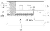
도 1 및 도 2를 참조하면, 기판(11) 상에 활성 영역(12)을 한정하는 소자 분리 막(13)이 형성될 수 있다. 상기 활성 영역(12) 상에 희생 패턴(15)이 형성될 수 있다(110). 상기 희생 패턴(15) 상에 바디(17)가 형성될 수 있다(120). 상기 희생 패턴(15) 및 상기 바디(17)의 측면들은 상기 소자 분리 막(13)에 의하여 둘러싸일 수 있다. 상기 바디(17) 상에 게이트 유전 막(21) 및 게이트 전극(23)이 차례로 형성될 수 있다(130). 상기 게이트 전극(23)을 덮는 층간 절연 막(25)이 형성될 수 있다(140). 상기 층간 절연 막(25)은 상기 기판(11)의 일면을 모두 덮을 수 있다.1 and 2, an
상기 기판(11)은 실리콘 웨이퍼와 같은 반도체 기판일 수 있다. 상기 활성 영역(12)은 P형 또는 N형 불순물들을 포함할 수 있다. 예를 들면, 상기 활성 영역(12)은 P형 불순물들을 갖는 단결정 실리콘일 수 있다. 상기 소자 분리 막(13)은 에스티아이(shallow trench isolation; STI) 기술을 이용하여 형성될 수 있다. 상기 소자 분리 막(13)은 실리콘 산화물, 실리콘 질화물, 실리콘 산질화물, 또는 이들의 조합과 같은 절연 층을 포함할 수 있다.The
상기 희생 패턴(15)은 상기 활성 영역(12)과 다른 물질을 포함할 수 있다. 상기 희생 패턴(15)은 상기 활성 영역(12)과 다른 물질을 포함하는 단결정 반도체일 수 있다. 예를 들면, 상기 활성 영역(12)은 단결정 실리콘을 포함할 수 있으며, 상기 희생 패턴(15)은 SiGe를 포함할 수 있다. 상기 희생 패턴(15)은 기체 상태 에피택시얼 성장(vapor phase epitaxial growth; VPE) 방법, 액체 상태 에피택시얼 성장(liquid phase epitaxial growth; LPE) 방법, 또는 고체 상태 에피택시얼 성장(solid phase epitaxial growth; SPE) 방법과 같은 제1 에피택시얼 성장 공정을 이용하여 상기 활성 영역(12) 상에 형성될 수 있다. 상기 희생 패턴(15)은 선택적 에피택시얼 성장(selective epitaxial growing; SEG) 방법을 이용하여 형성될 수 있다.The
상기 바디(17)는 반도체 층으로 지칭될 수 있다. 상기 바디(17)는 제2 에피택시얼 성장 공정을 이용하여 상기 희생 패턴(15) 상에 형성될 수 있다. 상기 바디(17)는 단결정 실리콘과 같은 단결정 반도체를 포함할 수 있다. 상기 바디(17)는 P형 또는 N형 불순물들을 포함할 수 있다. 예를 들면, 상기 바디(17)는 P형 불순물들을 갖는 단결정 실리콘일 수 있다. 상기 희생 패턴(15)은 상기 활성 영역(12) 및 상기 바디(17)에 접촉될 수 있다. 상기 희생 패턴(15)은 상기 활성 영역(12) 및 상기 바디(17)에 대하여 식각 선택비를 갖는 물질 막 일 수 있다. 상기 희생 패턴(15)은 상기 바디(17)와 다른 물질을 포함할 수 있다.The
상기 게이트 유전 막(21)은 실리콘 산화물, 실리콘 질화물, 실리콘 산질화물, high-K 물질, 또는 이들의 조합을 포함할 수 있다. 예를 들면, 상기 게이트 유전 막(21)은 열 산화 방법에 의한 실리콘 산화물일 수 있다. 상기 게이트 전극(23)은 상기 바디(17) 상을 가로지를 수 있다. 상기 게이트 전극(23)은 박막 형성 공정 및 패터닝 공정을 이용하여 형성될 수 있다. 상기 게이트 전극(23)은 폴리실리콘, 금속, 금속 실리사이드, 금속 질화물, 또는 이들의 조합과 같은 도전 체를 포함할 수 있다. 예를 들면, 상기 게이트 전극(23)은 폴리실리콘일 수 있다. 상기 층간 절연 막(25)은 실리콘 산화물, 실리콘 질화물, 실리콘 산질화물, 또는 이들의 조합을 포함할 수 있다. 예를 들면, 상기 층간 절연 막(25)은 실리콘 산화물일 수 있다.The
다른 실시 예에서, 상기 층간 절연 막(25) 내에 상기 게이트 유전 막(21) 및 상기 게이트 전극(23)을 포함한 다양한 종류의 능동/수동 소자들이 추가적으로 형성될 수 있다. 예를 들면, 상기 바디(17) 상에 스위칭 소자들 및/또는 다양한 종류의 데이터 저장 요소들이 형성될 수 있다. 상기 스위칭 소자들은 다이오드 또는 트랜지스터를 포함할 수 있다. 상기 데이터 저장 요소들은 차지 트랩 막(charge trap layer), 상-변화 물질 막(phase-change material layer), 저항 변화 물질 막(resistive change material layer), 커패시터(capacitor), 또는 엠티제이(magnetic tunnel junction; MTJ)를 포함할 수 있다.In another embodiment, various kinds of active / passive elements including the
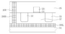
도 1 및 도 3을 참조하면, 상기 층간 절연 막(25) 및 상기 바디(17)를 관통하여 상기 희생 패턴(15)을 노출하는 콘택 홀(25H)이 형성될 수 있다. 상기 콘택 홀(25H)의 형성에는 사진 공정 및 식각 공정을 포함하는 패터닝 공정이 적용될 수 있다.Referring to FIGS. 1 and 3, a
도 1 및 도 4를 참조하면, 상기 희생 패턴(15)을 제거하여 빈 공간(15V)이 형성될 수 있다(150). 상기 빈 공간(15V)은 상기 콘택 홀(25H)에 연통될 수 있다. 상기 빈 공간(15V)에 의하여 상기 바디(17) 및 상기 활성 영역(12)이 노출될 수 있다.Referring to FIGS. 1 and 4, an
도 1 및 도 5를 참조하면, 상기 빈 공간(15V) 및 상기 콘택 홀(25H) 내부를 채우고 상기 층간 절연 막(25)을 덮는 비정질 실리콘 막(amorphous silicon layer; 29)이 형성될 수 있다(160). 상기 비정질 실리콘 막(29)은 매우 우수한 매립특성을 보일 수 있다. 상기 빈 공간(15V) 및 상기 콘택 홀(25H)이 길고 구부러진 구조라 할지라도, 상기 빈 공간(15V) 및 상기 콘택 홀(25H)은 상기 비정질 실리콘 막(29)에 의하여 치밀하게 매립될 수 있다. 상기 비정질 실리콘 막(29)은 상기 활성 영역(12) 및 상기 바디(17)에 접촉될 수 있다.1 and 5, an
도 1 및 도 6을 참조하면, 상기 비정질 실리콘 막(29)을 평탄화하여 상기 층간 절연 막(25)이 노출될 수 있다. 상기 비정질 실리콘 막(29)은 상기 콘택 홀(25H) 및 상기 빈 공간(15V) 내에 보존될 수 있다.Referring to FIGS. 1 and 6, the
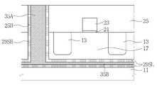
도 1 및 도 7을 참조하면, 상기 층간 절연 막(25) 상에 금속 막(31) 및 캐핑 막(33)이 차례로 형성될 수 있다. 상기 금속 막(31)은 상기 비정질 실리콘 막(29)에 접촉될 수 있다. 상기 금속 막(31)은 Co, Ni, Ti, Ta, W, 또는 이들의 조합을 포함할 수 있다. 상기 캐핑 막(33)은 상기 금속 막(31) 상을 덮을 수 있다. 상기 캐핑 막(33)은 TiN과 같은 금속 질화물을 포함할 수 있다.Referring to FIGS. 1 and 7, a
도 1 및 도 8을 참조하면, 실리사이드 변환 공정을 이용하여 금속 실리사이드 막(29SH, 29SL)이 형성될 수 있다(170). 상기 금속 실리사이드 막(29SH, 29SL)의 형성에는 상기 금속 막(31) 및 상기 비정질 실리콘 막(29)을 열처리하는 공정이 포함될 수 있다. 예를 들면, 상기 금속 막(31) 및 상기 비정질 실리콘 막(29)의 열처리는 약400 ℃ 온도에서 수행될 수 있다. 상기 금속 실리사이드 막(29SH, 29SL)은 CoSi, NiSi, TiSi, TaSi, WSi, 또는 이들의 조합을 포함할 수 있다. 상기 금속 실리사이드 막(29SH, 29SL)은 상기 콘택 홀(25H) 내에 형성된 금속 실리사이드 플러그(29SH) 및 상기 빈 공간(15V) 내에 형성된 금속 실리사이드 패턴(29SL)을 포함할 수 있다. 상기 금속 실리사이드 패턴(29SL)은 상기 금속 실리사이드 플러그(29SH)에 연속될(in continuity with) 수 있다. 상기 금속 실리사이드 패턴(29SL)은 상기 활성 영역(12) 및 상기 바디(17)에 접촉될 수 있다.Referring to FIGS. 1 and 8, metal silicide films 29SH and 29SL may be formed 170 using a silicide conversion process. The formation of the metal silicide films 29SH and 29SL may include a step of heat-treating the
본 발명자들이 확인한 바에 의하면, 상기 비정질 실리콘 막(29)은 단결정 실리콘에 비하여 금속과의 반응에너지가 낮은 것으로 나타났다. 상기 금속 막(31)과 상기 비정질 실리콘 막(29) 간의 반응에너지는 상기 금속 막(31)과 상기 활성 영역(12) 간의 반응에너지보다 낮을 수 있다. 또한, 상기 금속 막(31)과 상기 비정질 실리콘 막(29) 간의 반응에너지는 상기 금속 막(31)과 상기 바디(17) 간의 반응에너지보다 낮을 수 있다. 상기 금속 막(31)에 포함된 금속은 상기 비정질 실리콘 막(29)과 선택적으로 결합되어 상기 금속 실리사이드 막(29SH, 29SL)이 형성될 수 있다.The present inventors have found that the
도 1 및 도 9를 참조하면, 상기 캐핑 막(33) 및 상기 금속 막(31)을 제거하여 상기 금속 실리사이드 플러그(29SH) 및 상기 층간 절연 막(25)이 노출될 수 있다.Referring to FIGS. 1 and 9, the
본 발명 기술적 사상의 실시 예들에 따르면, 상기 금속 실리사이드 막(29SH, 29SL)은 상기 게이트 유전 막(21) 및 상기 게이트 전극(23)을 포함하는 능동 소자들보다 나중에 형성될 수 있다. 상기 금속 실리사이드 막(29SH, 29SL)의 형성 방법은 금속 물질 오염에 의한 능동 소자들의 전기적 특성 저하를 방지할 수 있다. 또한, 상기 금속 실리사이드 막(29SH, 29SL)은 불순물 도핑(doping)된 실리콘 패턴에 비하여 낮은 전기 저항을 보인다. 상기 금속 실리사이드 막(29SH, 29SL)은 불순물 도핑(doping)된 실리콘 패턴에 비하여 매우 우수한 전류 구동 능력을 가질 수 있다. 상기 금속 실리사이드 막(29SH, 29SL)에 기인하여 본 발명 기술적 사상의 실시 예들에 따른 반도체 소자는 고집적화에 매우 유리할 수 있다.According to embodiments of the present invention, the metal silicide films 29SH and 29SL may be formed later than the active elements including the
도 10 내지 도 14는 본 발명 기술적 사상의 일 실시 예에 따른 반도체 소자의 형성 방법을 설명하기 위한 공정 단면도들 이다.FIGS. 10 to 14 are process cross-sectional views illustrating a method of forming a semiconductor device according to an embodiment of the present invention.
도 1 및 도 10을 참조하면, 비정질 실리콘 막(29)을 에치-백(etch-back)하여 콘택 홀(25H)이 부분적으로 노출될 수 있다. 상기 비정질 실리콘 막(29)은 상기 콘택 홀(25H)의 하단 영역 및 상기 빈 공간(도 4의 15V) 내에 보존될 수 있다. 상기 비정질 실리콘 막(29)의 상단은 상기 바디(17)보다 높은 레벨에 보존될 수 있다.Referring to FIGS. 1 and 10, the
도 1 및 도 11을 참조하면, 상기 층간 절연 막(25) 상에 금속 막(31) 및 캐핑 막(33)이 차례로 형성될 수 있다. 상기 금속 막(31)은 상기 콘택 홀(25H)을 채울 수 있다. 상기 금속 막(31)은 상기 비정질 실리콘 막(29)에 접촉될 수 있다. 상기 캐핑 막(33)은 상기 금속 막(31) 상을 덮을 수 있다.Referring to FIGS. 1 and 11, a
도 1 및 도 12를 참조하면, 실리사이드 변환 공정을 이용하여 금속 실리사이드 막(29SH, 29SL)이 형성될 수 있다(170). 상기 금속 실리사이드 막(29SH, 29SL)은 상기 콘택 홀(25H) 내에 형성된 금속 실리사이드 플러그(29SH) 및 상기 빈 공간(도 4의 15V) 내에 형성된 금속 실리사이드 패턴(29SL)을 포함할 수 있다. 상기 금속 실리사이드 패턴(29SL)은 상기 활성 영역(12) 및 상기 바디(17)에 접촉될 수 있다.Referring to FIGS. 1 and 12, metal silicide films 29SH and 29SL may be formed (170) using a silicide conversion process. The metal silicide films 29SH and 29SL may include a metal silicide plug 29SH formed in the
도 1 및 도 13을 참조하면, 상기 캐핑 막(33) 및 상기 금속 막(31)을 제거하여 상기 금속 실리사이드 플러그(29SH) 및 상기 층간 절연 막(25)이 노출될 수 있다. 상기 금속 실리사이드 플러그(29SH) 상에 상기 콘택 홀(25H)의 상단영역이 노출될 수 있다.Referring to FIGS. 1 and 13, the
도 1 및 도 14를 참조하면, 상기 콘택 홀(25H)의 상단영역을 채우는 도전성 플러그(35)가 형성될 수 있다. 상기 도전성 플러그(35)는 박막 형성 공정 및 평탄화 공정을 이용하여 형성될 수 있다. 상기 도전성 플러그(35)는 상기 금속 실리사이드 플러그(29SH)에 접촉될 수 있다. 상기 도전성 플러그(35)는 금속, 금속 질화물, 금속 실리사이드, 도전성 카본 그룹, 폴리실리콘, 또는 이들의 조합을 포함할 수 있다. 예를 들면, 상기 도전성 플러그(35)는 W, WN, TiN, TaN, Ru, 또는 이들의 조합을 포함할 수 있다.Referring to FIGS. 1 and 14, a
도 15 내지 도 20은 본 발명 기술적 사상의 일 실시 예에 따른 반도체 소자의 형성 방법을 설명하기 위한 공정 단면도들 이다.15 to 20 are process cross-sectional views illustrating a method of forming a semiconductor device according to an embodiment of the present invention.
도 1 및 도 15를 참조하면, 상기 콘택 홀(25H)의 측벽을 덮고, 상기 빈 공간(도 4의 15V)을 채우며, 상기 층간 절연 막(25)을 덮는 비정질 실리콘 막(amorphous silicon layer; 29)이 형성될 수 있다(160). 상기 비정질 실리콘 막(29)은 매우 우수한 표면 피복 특성을 보일 수 있다. 상기 비정질 실리콘 막(29)은 상기 콘택 홀(25H)의 측벽을 일정한 두께로 덮을 수 있다.Referring to FIGS. 1 and 15, an amorphous silicon layer (an amorphous silicon layer) 29, which covers the sidewalls of the contact holes 25H, fills the voids (15V in FIG. 4) May be formed (160). The
도 1 및 도 16을 참조하면, 상기 비정질 실리콘 막(29) 상에 금속 막(31) 및 캐핑 막(33)이 차례로 형성될 수 있다. 상기 금속 막(31) 및 상기 캐핑 막(33)은 상기 콘택 홀(25H)을 채울 수 있다. 상기 금속 막(31)은 상기 비정질 실리콘 막(29)에 접촉될 수 있다.Referring to FIGS. 1 and 16, a
도 1 및 도 17을 참조하면, 실리사이드 변환 공정을 이용하여 금속 실리사이드 막(29S, 29SH, 29SL)이 형성될 수 있다(170). 상기 금속 실리사이드 막(29S, 29SH, 29SL)은 상기 콘택 홀(25H) 내에 형성된 금속 실리사이드 플러그(29SH) 및 상기 빈 공간(도 4의 15V) 내에 형성된 금속 실리사이드 패턴(29SL)을 포함할 수 있다. 상기 금속 실리사이드 패턴(29SL)은 상기 활성 영역(12) 및 상기 바디(17)에 접촉될 수 있다.Referring to FIGS. 1 and 17,
도 1 및 도 18을 참조하면, 상기 캐핑 막(33), 상기 금속 막(31) 및 상기 금속 실리사이드 막(29S, 29SH, 29SL)을 평탄화하여 상기 층간 절연 막(25)이 노출될 수 있다. 상기 캐핑 막(33), 상기 금속 막(31) 및 상기 금속 실리사이드 플러그(29SH)는 상기 콘택 홀(25H) 내에 보존될 수 있다.Referring to FIGS. 1 and 18, the
도 1 및 도 19를 참조하면, 상기 콘택 홀(25H) 내에 남은 상기 캐핑 막(33) 및 상기 금속 막(31)이 제거될 수 있다.Referring to FIGS. 1 and 19, the capping
도 1 및 도 20을 참조하면, 상기 콘택 홀(25H) 내에 코어(core; 35A)가 형성될 수 있다(180). 상기 코어(35A)는 박막 형성 공정 및 평탄화 공정을 이용하여 형성될 수 있다. 상기 금속 실리사이드 플러그(29SH)는 상기 코어(35A)의 측면을 감쌀 수 있다. 상기 코어(35A)는 상기 금속 실리사이드 플러그(29SH)에 접촉될 수 있다. 상기 코어(35A)는 금속, 금속 질화물, 금속 실리사이드, 도전성 카본 그룹, 폴리실리콘, 또는 이들의 조합을 포함할 수 있다. 예를 들면, 상기 코어(35A)는 W, WN, TiN, TaN, Ru, 또는 이들의 조합을 포함할 수 있다.Referring to FIGS. 1 and 20, a
도 21 내지 도 23은 본 발명 기술적 사상의 일 실시 예에 따른 반도체 소자의 형성 방법을 설명하기 위한 공정 단면도들 이다.21 to 23 are process sectional views for explaining a method of forming a semiconductor device according to an embodiment of the present invention.
도 1 및 도 21을 참조하면, 상기 콘택 홀(25H) 및 상기 빈 공간(15V)의 측벽을 덮고, 상기 층간 절연 막(25)을 덮는 비정질 실리콘 막(amorphous silicon layer; 29)이 형성될 수 있다(160). 상기 비정질 실리콘 막(29)은 상기 콘택 홀(25H) 및 상기 빈 공간(15V)의 측벽을 일정한 두께로 덮을 수 있다. 상기 콘택 홀(25H) 및 상기 빈 공간(15V)은 상기 비정질 실리콘 막(29)에 의하여 축소될 수 있다. 상기 비정질 실리콘 막(29)은 상기 활성 영역(12) 및 상기 바디(17)에 접촉될 수 있다.1 and 21, an
상기 비정질 실리콘 막(29)은 매우 우수한 표면 피복 특성을 보일 수 있다. 상기 콘택 홀(25H) 및 상기 빈 공간(15V)이 길고, 좁고, 구부러지고, 복잡하다 할지라도, 상기 비정질 실리콘 막(29)은 상기 콘택 홀(25H)의 측벽 및 상기 빈 공간(15V)의 내벽들 상에 끊어지지 않고 일정한 두께로 형성될 수 있다.The
도 1 및 도 22를 참조하면, 상기 비정질 실리콘 막(29) 상에 금속 막(31) 및 캐핑 막(33)이 차례로 형성될 수 있다. 실리사이드 변환 공정을 이용하여 금속 실리사이드 막(29S, 29SH, 29SL)이 형성될 수 있다(170).Referring to FIGS. 1 and 22, a
상기 금속 막(31)은 상기 콘택 홀(25H) 및 상기 빈 공간(15V)을 채울 수 있다. 상기 금속 실리사이드 막(29S, 29SH, 29SL)은 상기 콘택 홀(25H) 내에 형성된 금속 실리사이드 플러그(29SH) 및 상기 빈 공간(15V) 내에 형성된 금속 실리사이드 패턴(29SL)을 포함할 수 있다. 상기 금속 실리사이드 패턴(29SL)은 상기 활성 영역(12) 및 상기 바디(17)에 접촉될 수 있다.The
도 1 및 도 23을 참조하면, 금속 막(31) 및 캐핑 막(33)을 제거하고 상기 콘택 홀(25H) 및 상기 빈 공간(15V) 내에 코어(core; 35A, 35B)가 형성될 수 있다(180). 상기 코어(35A, 35B)는 박막 형성 공정 및 평탄화 공정을 이용하여 형성될 수 있다. 상기 코어(35A, 35B)는 상기 콘택 홀(25H) 내에 형성된 코어 플러그(35A) 및 상기 빈 공간(15V) 내에 형성된 코어 패턴(35B)을 포함할 수 있다. 상기 코어 패턴(35B)은 상기 코어 플러그(35A)에 연속될(in continuity with)수 있다. 상기 코어(35A, 35B)는 금속, 금속 질화물, 금속 실리사이드, 도전성 카본 그룹, 폴리실리콘, 또는 이들의 조합을 포함할 수 있다. 예를 들면, 상기 코어(35A, 35B)는 W, WN, TiN, TaN, Ru, 또는 이들의 조합을 포함할 수 있다.1 and 23,
상기 금속 실리사이드 플러그(29SH)는 상기 코어 플러그(35A)의 측면을 감쌀 수 있다. 상기 코어 플러그(35A)는 상기 금속 실리사이드 플러그(29SH)에 접촉될 수 있다. 상기 금속 실리사이드 패턴(29SL)은 상기 코어 패턴(35B)의 상면 및 하부표면을 감쌀 수 있다. 상기 금속 실리사이드 패턴(29SL)은 상기 코어 패턴(35B)에 접촉될 수 있다.The metal silicide plug 29SH may cover the side surface of the
도 24 및 도 25는 본 발명 기술적 사상의 일 실시 예에 따른 반도체 소자의 형성 방법을 설명하기 위한 공정 단면도들 이다.24 and 25 are process sectional views for explaining a method of forming a semiconductor device according to one embodiment of the technical idea of the present invention.
도 24를 참조하면, 기판(11) 상에 희생 패턴(15)이 형성될 수 있다. 상기 희생 패턴(15) 상에 바디(17)가 형성될 수 있다. 상기 바디(17) 내에 소자 분리 막(13)이 형성될 수 있다. 상기 바디(17) 상에 게이트 유전 막(21) 및 게이트 전극(23)이 차례로 형성될 수 있다. 상기 게이트 전극(23)을 덮는 층간 절연 막(25)이 형성될 수 있다.Referring to FIG. 24, a
상기 기판(11)은 P형 불순물들을 갖는 단결정 실리콘을 포함할 수 있다. 상기 희생 패턴(15)은 상기 기판(11)의 일정영역을 덮는 플레이트 모양일 수 있다. 상기 희생 패턴(15)은 상기 기판(11)과 다른 물질을 포함할 수 있다. 예를 들면, 상기 희생 패턴(15)은 SiGe를 포함할 수 있다. 상기 희생 패턴(15)은 에피택시얼 성장 기술을 이용하여 형성될 수 있다. 상기 바디(17)는 에피택시얼 성장 기술을 이용하여 상기 희생 패턴(15) 상에 형성될 수 있다. 상기 바디(17)는 P형 불순물들을 갖는 단결정 실리콘을 포함할 수 있다. 상기 희생 패턴(15)은 상기 기판(11) 및 상기 바디(17)에 대하여 식각 선택비를 갖는 물질 막 일 수 있다. 상기 희생 패턴(15)은 상기 바디(17)와 다른 물질을 포함할 수 있다.The
도 25를 참조하면, 상기 층간 절연 막(25) 및 상기 바디(17)를 관통하여 상기 희생 패턴(15)을 노출하는 콘택 홀(25H)을 형성하고, 상기 희생 패턴(15)을 제거한 후, 실리사이드 변환 공정을 이용하여 금속 실리사이드 막(29SH, 29SL)이 형성될 수 있다. 상기 금속 실리사이드 막(29SH, 29SL)은 금속 실리사이드 플러그(29SH) 및 금속 실리사이드 패턴(29SL)을 포함할 수 있다. 상기 금속 실리사이드 패턴(29SL)은 상기 기판(11) 및 상기 바디(17)에 접촉될 수 있다.25, a
도 26은 본 발명 기술적 사상의 일 실시 예에 따른 반도체 소자의 형성 방법을 설명하기 위한 공정 단면도 이다.26 is a cross-sectional view illustrating a method of forming a semiconductor device according to an embodiment of the present invention.
도 26을 참조하면, 콘택 홀(25H)의 상단 영역에 도전성 플러그(35)가 형성될 수 있다. 상기 도전성 플러그(35)는 금속 실리사이드 플러그(29SH)에 접촉될 수 있다. 상기 금속 실리사이드 플러그(29SH)는 상기 콘택 홀(25H)의 하단 영역에 형성될 수 있다.Referring to FIG. 26, a
도 27은 본 발명 기술적 사상의 일 실시 예에 따른 반도체 소자의 형성 방법을 설명하기 위한 공정 단면도 이다.27 is a process sectional view for explaining a method of forming a semiconductor device according to an embodiment of the present invention.
도 27을 참조하면, 코어(core; 35A, 35B) 및 상기 코어(35A, 35B)를 감싸는 금속 실리사이드 막(29SH, 29SL)이 형성될 수 있다. 상기 금속 실리사이드 막(29SH, 29SL)은 금속 실리사이드 플러그(29SH) 및 금속 실리사이드 패턴(29SL)을 포함할 수 있다. 상기 금속 실리사이드 패턴(29SL)은 상기 기판(11) 및 상기 바디(17)에 접촉될 수 있다. 상기 코어(35A, 35B)는 코어 플러그(35A) 및 코어 패턴(35B)을 포함할 수 있다. 상기 코어 패턴(35B)은 상기 코어 플러그(35A)에 연속될(in continuity with)수 있다.Referring to FIG. 27, metal silicide films 29SH and 29SL that surround the
상기 금속 실리사이드 플러그(29SH)는 상기 코어 플러그(35A)의 측면을 감쌀 수 있다. 상기 코어 플러그(35A)는 상기 금속 실리사이드 플러그(29SH)에 접촉될 수 있다. 상기 금속 실리사이드 패턴(29SL)은 상기 코어 패턴(35B)의 상면 및 하부표면을 덮을 수 있다. 상기 금속 실리사이드 패턴(29SL)은 상기 코어 패턴(35B)에 접촉될 수 있다.The metal silicide plug 29SH may cover the side surface of the
도 28 내지 도 38은 본 발명 기술적 사상의 일 실시 예에 따른 반도체 소자의 형성 방법을 설명하기 위한 공정 단면도들 이다.28 to 38 are process sectional views for explaining a method of forming a semiconductor device according to an embodiment of the technical idea of the present invention.
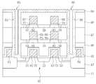
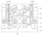
도 28을 참조하면, 반도체 기판(41) 상에 활성 영역(42)을 한정하는 소자 분리 막(43)이 형성될 수 있다. 상기 반도체 기판(41) 상에 제1 내지 제8 게이트 전극들(61, 62, 63, 64, 65, 66, 67, 68), 게이트 유전 막들(72, 73, 75, 76, 77, 78), 제1 내지 제9 소스/드레인 영역들(51, 52, 53, 54, 55, 56, 57, 58, 59), 바디들(81, 82, 83, 84), 식각 정지 막(45), 및 제1 내지 제3 절연 막들(46, 47, 48)이 형성될 수 있다. 상기 제2 게이트 전극(62) 및 제3 게이트 전극(63)의 각각은 SRAM 셀(cell)의 풀-다운(pull-down) 트랜지스터를 구성할 수 있으며, 상기 제5 게이트 전극(65) 및 제6 게이트 전극(66)의 각각은 SRAM 셀의 로드(load) 트랜지스터를 구성할 수 있고, 상기 제7 게이트 전극(67) 및 제8 게이트 전극(68)의 각각은 SRAM 셀의 패스(pass) 트랜지스터를 구성할 수 있다.Referring to Fig. 28, an
도 29를 참조하면, 상기 제1 내지 제3 절연 막들(46, 47, 48) 및 상기 식각 정지 막(45)을 관통하는 제1 및 제2 콘택 홀들(85, 86)이 형성될 수 있다. 상기 제1 콘택 홀(85) 내에 상기 제1 게이트 전극(61), 상기 제1 소스/드레인 영역(51), 상기 제4 소스/드레인 영역(54), 및 상기 제7 소스/드레인 영역(57)이 노출될 수 있다. 상기 제2 콘택 홀(86) 내에 상기 제4 게이트 전극(64), 상기 제3 소스/드레인 영역(53), 상기 제6 소스/드레인 영역(56), 및 상기 제9 소스/드레인 영역(59)이 노출될 수 있다.Referring to FIG. 29, first and second contact holes 85 and 86 penetrating the first to third insulating
도 30을 참조하면, 상기 제1 게이트 전극(61), 상기 제4 게이트 전극(64), 상기 제1 소스/드레인 영역(51), 상기 제3 소스/드레인 영역(53), 상기 제4 소스/드레인 영역(54), 상기 제6 소스/드레인 영역(56), 상기 제7 소스/드레인 영역(57), 및 상기 제9 소스/드레인 영역(59)을 부분적으로 제거하여 빈 공간들(51V, 53V, 54V, 56V, 57V, 59V)이 형성될 수 있다.Referring to FIG. 30, the
다른 실시 예에서, 상기 제1 소스/드레인 영역(51), 상기 제3 소스/드레인 영역(53), 상기 제4 소스/드레인 영역(54), 상기 제6 소스/드레인 영역(56), 상기 제7 소스/드레인 영역(57), 및 상기 제9 소스/드레인 영역(59) 중 적어도 하나는 완전히 제거될 수 있다. 또 다른 실시 예에서, 상기 제1 소스/드레인 영역(51), 상기 제3 소스/드레인 영역(53), 상기 제4 소스/드레인 영역(54), 상기 제6 소스/드레인 영역(56), 상기 제7 소스/드레인 영역(57), 및 상기 제9 소스/드레인 영역(59)은 완전히 제거될 수 있다.In another embodiment, the first source /
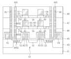
도 31을 참조하면, 상기 제1 및 제2 콘택 홀들(85, 86), 및 상기 빈 공간들(51V, 53V, 54V, 56V, 57V, 59V) 내에 비정질 실리콘 막(amorphous silicon layer; 89)이 형성될 수 있다. 상기 비정질 실리콘 막(89)은 매우 우수한 표면 피복 특성을 보일 수 있다.31, an
도 32를 참조하면, 상기 비정질 실리콘 막(89) 상에 금속 막(91) 및 캐핑 막(93)이 차례로 형성될 수 있다.Referring to FIG. 32, a
도 33을 참조하면, 실리사이드 변환 공정을 이용하여 금속 실리사이드 막(89S)이 형성될 수 있다. 상기 금속 실리사이드 막(89S)은 제1 내지 제3 금속 실리사이드 패턴들(89SA, 89SB, 89SC)을 포함할 수 있다. 상기 제1 금속 실리사이드 패턴(89SA)은 상기 제1 소스/드레인 영역(51)에 접촉될 수 있으며, 상기 제2 금속 실리사이드 패턴(89SB)은 상기 제4 소스/드레인 영역(54)에 접촉될 수 있고, 상기 제3 금속 실리사이드 패턴(89SC)은 상기 제7 소스/드레인 영역(57)에 접촉될 수 있다.Referring to FIG. 33, a
도 34를 참조하면, 상기 캐핑 막(93), 상기 금속 막(91) 및 상기 금속 실리사이드 막(89S)을 평탄화하여 상기 제3 절연 막(48)이 노출될 수 있다. 상기 금속 막(91)은 상기 제1 및 제2 콘택 홀들(85, 86) 내에 잔존할 수 있다.Referring to FIG. 34, the capping
도 35를 참조하면, 상기 금속 막(91)은 완전히 제거될 수 있다.Referring to FIG. 35, the
도 36을 참조하면, 상기 제1 및 제2 콘택 홀들(85, 86) 내에 코어들(95)이 형성될 수 있다.Referring to FIG. 36,
도 37을 참조하면, 상기 제3 절연 막(48) 상에 제4 절연 막(49)이 형성될 수 있다. 상기 제4 절연 막(49) 및 상기 제3 절연 막(48)을 관통하여 상기 제8 소스/드레인 영역(58)을 노출하는 제3 콘택 홀(49H)이 형성될 수 있다.Referring to FIG. 37, a fourth insulating
도 38을 참조하면, 상기 제3 콘택 홀(49H) 내에 비트 플러그(97)가 형성될 수 있다.Referring to FIG. 38, a
도 39 내지 도 42는 본 발명 기술적 사상의 일 실시 예에 따른 반도체 소자의 형성 방법을 설명하기 위한 공정 단면도들 이다. 도 39 내지 도 42에 도시된 반도체 소자는 낸드 플래시 메모리(NAND flash memory)의 셀 영역 및 주변 회로 영역의 일부분일 수 있다.39 to 42 are process sectional views for explaining a method of forming a semiconductor device according to an embodiment of the technical idea of the present invention. The semiconductor device shown in Figs. 39 to 42 may be a part of a cell region and a peripheral circuit region of a NAND flash memory.
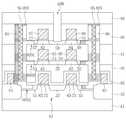
도 39를 참조하면, 반도체 기판(211) 상에 희생 패턴(215), 제1 내지 제10 절연 막들(241, 242, 243, 244, 245, 246, 247, 248, 249, 250), 제1 및 제2 그라운드 선택 게이트 전극들(261, 262), 제1 내지 제4 컨트롤 게이트 전극들(263, 264, 265, 266), 제1 및 제2 스트링 선택 게이트 전극들(267, 268), 제1 및 제2 전하 트랩 유전 막들(221, 222), 바디들(217), 도전성 플러그들(251), 드레인 영역들(252), 절연성 코어들(255), 비트 라인들(257), 및 제11 절연 막(259)이 형성될 수 있다.Referring to FIG. 39, a
상기 반도체 기판(211)은 P형 불순물을 갖는 단결정 실리콘을 포함할 수 있으며, 상기 희생 패턴(215)은 SiGe를 포함할 수 있고, 상기 바디들(217)은 폴리실리콘 또는 단결정 실리콘을 포함할 수 있다. 상기 제1 및 제2 그라운드 선택 게이트 전극들(261, 262), 상기 제1 내지 제4 컨트롤 게이트 전극들(263, 264, 265, 266), 및 상기 제1 및 제2 스트링 선택 게이트 전극들(267, 268)은 금속, 금속 실리사이드, 금속 질화물, 폴리실리콘, 또는 이들의 조합과 같은 도전 체를 포함할 수 있다. 상기 제1 및 제2 전하 트랩 유전 막들(221, 222)은 실리콘 산화물, 실리콘 질화물, 실리콘 산질화물, 금속 산화물, 금속 실리케이트, 또는 이들의 조합을 포함할 수 있다. 예를 들면, 상기 제1 전하 트랩 유전 막들(221)은 제1 실리콘 산화물, 실리콘 질화물, 및 제2 실리콘 산화물이 차례로 적층된 구조체를 포함하고, 상기 제2 전하 트랩 유전 막들(222)은 AlO를 포함할 수 있다.The
도 40을 참조하면, 상기 제10 절연 막(250) 및 상기 제11 절연 막(259)을 관통하는 콘택 홀(259H), 및 희생 패턴(215)을 제거하여 형성된 빈 공간(215V)이 형성될 수 있다. 상기 빈 공간(215V) 내에 상기 반도체 기판(211) 및 상기 바디들(217)이 노출될 수 있다.40, a
도 41을 참조하면, 상기 콘택 홀(259H) 및 상기 빈 공간(215V) 내에 비정질 실리콘 막(amorphous silicon layer; 229)이 형성될 수 있다. 상기 비정질 실리콘 막(229) 상에 금속 막(231) 및 캐핑 막(233)이 차례로 형성될 수 있다.Referring to FIG. 41, an
도 42를 참조하면, 실리사이드 변환 공정을 이용하여 금속 실리사이드 막(229SH, 229SL)이 형성될 수 있다. 상기 금속 실리사이드 막(229SH, 229SL)은 금속 실리사이드 플러그(229SH) 및 금속 실리사이드 패턴(229SL)을 포함할 수 있다. 상기 금속 실리사이드 패턴(229SL)은 상기 반도체 기판(211) 및 상기 바디(217)에 접촉될 수 있다. 상기 금속 막(231) 및 상기 캐핑 막(233)을 제거하고 코어(core; 235A, 235B)가 형성될 수 있다. 상기 코어(235A, 235B)는 코어 플러그(235A) 및 코어 패턴(235B)을 포함할 수 있다.Referring to FIG. 42, metal silicide films 229SH and 229SL may be formed using a silicide conversion process. The metal silicide films 229SH and 229SL may include a metal silicide plug 229SH and a metal silicide pattern 229SL. The metal silicide pattern 229SL may be in contact with the
도 43은 본 발명 기술적 사상의 일 실시 예에 따른 반도체 소자의 형성 방법을 설명하기 위한 공정 단면도 이다.43 is a cross-sectional view illustrating a method of forming a semiconductor device according to an embodiment of the present invention.
도 43을 참조하면, 콘택 홀(259H) 내에 코어 플러그(235A)가 형성될 수 있다. 금속 실리사이드 플러그(229SH)는 상기 코어 플러그(235A)의 측면을 감쌀 수 있다. 상기 금속 실리사이드 플러그(229SH)의 하단에 연속된 금속 실리사이드 패턴(229SL)이 형성될 수 있다.Referring to FIG. 43, a
도 44 및 도 45는 본 발명 기술적 사상의 일 실시 예에 따른 반도체 소자의 형성 방법을 설명하기 위한 공정 단면도들 이다.44 and 45 are process sectional views for explaining a method of forming a semiconductor device according to an embodiment of the technical idea of the present invention.
도 44를 참조하면, 반도체 기판(211) 내에 소스 영역들(216)이 형성될 수 있다. 상기 소스 영역들(216) 내에 희생 패턴들(215)이 형성될 수 있다. 상기 희생 패턴들(215) 상에 제11 절연 막들(259)이 형성될 수 있다. 바디들(217)은 상기 반도체 기판(211)에 접촉될 수 있다. 상기 소스 영역들(216)은 N형 불순물들을 갖는 단결정 실리콘을 포함할 수 있다.Referring to FIG. 44,
도 45를 참조하면, 상기 희생 패턴들(215)을 제거한 후, 금속 실리사이드 패턴들(229SL) 및 코어 패턴들(235B)이 형성될 수 있다. 상기 금속 실리사이드 패턴들(229SL)은 상기 코어 패턴들(235B)을 둘러쌀 수 있다. 상기 금속 실리사이드 패턴들(229SL)은 상기 소스 영역들(216) 내에 형성될 수 있다. 상기 금속 실리사이드 패턴들(229SL)은 상기 소스 영역들(216)에 접촉될 수 있다.Referring to FIG. 45, after the
도 46 내지 도 49는 본 발명 기술적 사상의 일 실시 예에 따른 반도체 소자의 형성 방법을 설명하기 위한 공정 단면도들 이다. 도 46 내지 도 49에 도시된 반도체 소자는 상변화 메모리의 셀 영역 및 주변 회로 영역의 일부분일 수 있다.46 to 49 are process sectional views for explaining a method of forming a semiconductor device according to an embodiment of the technical idea of the present invention. The semiconductor device shown in Figs. 46 to 49 may be a part of the cell region and the peripheral circuit region of the phase-change memory.
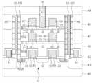
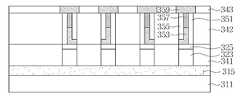
도 46을 참조하면, 반도체 기판(311) 상에 희생 패턴(315), 제1 내지 제3 절연 막들(341, 342, 343), 스위칭 소자들(323), 스위칭 전극들(325), 하부 전극들(353), 스페이서들(351, 355), 데이터 저장 요소들(357), 및 상부 전극들(359)이 형성될 수 있다.46, a
상기 반도체 기판(311)은 P형 불순물들을 갖는 단결정 실리콘을 포함할 수 있다. 상기 희생 패턴(315)은 SiGe를 포함할 수 있다. 상기 스위칭 소자들(323)은 다이오드를 포함할 수 있다. 상기 스위칭 소자들(323)의 각각은 P형 불순물들을 갖는 단결정 실리콘을 포함할 수 있다. 상기 스위칭 전극들(325)은 금속 실리사이드, 금속 질화물, 금속, 또는 이들의 조합과 같은 도전 체를 포함할 수 있다. 상기 데이터 저장 요소들(357)은 GST와 같은 상변화 물질을 포함할 수 있다.The
도 47을 참조하면, 상기 제1 내지 제3 절연 막들(341, 342, 343)을 관통하는 콘택 홀(341H), 및 상기 희생 패턴(315)을 제거하여 형성된 빈 공간(315V)이 형성될 수 있다.Referring to FIG. 47, a
도 48을 참조하면, 상기 콘택 홀(341H) 및 상기 빈 공간(315V)내에 비정질 실리콘 막(329), 금속 막(331) 및 캐핑 막(333)이 형성될 수 있다.Referring to FIG. 48, an
도 49를 참조하면, 실리사이드 변환 공정을 이용하여 금속 실리사이드 막(329SH, 329SL)이 형성될 수 있다. 상기 금속 실리사이드 막(329SH, 329SL)은 금속 실리사이드 플러그(329SH) 및 금속 실리사이드 패턴(329SL)을 포함할 수 있다. 상기 금속 실리사이드 패턴(329SL)은 상기 반도체 기판(311) 및 상기 스위칭 소자들(323)에 접촉될 수 있다. 상기 금속 막(331) 및 상기 캐핑 막(333)을 제거하고 코어(core; 335A, 335B)가 형성될 수 있다. 상기 코어(335A, 335B)는 코어 플러그(335A) 및 코어 패턴(335B)을 포함할 수 있다.Referring to FIG. 49,
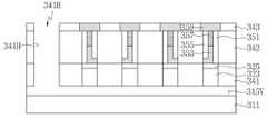
도 50은 본 발명 기술적 사상의 일 실시 예에 따른 반도체 소자의 형성 방법을 설명하기 위한 공정 단면도 이다.50 is a cross-sectional view illustrating a method of forming a semiconductor device according to an embodiment of the present invention.
도 50을 참조하면, 콘택 홀(341H) 내에 코어 플러그(335)가 형성될 수 있다. 금속 실리사이드 플러그(329SH)는 상기 코어 플러그(335)의 측면을 감쌀 수 있다. 상기 금속 실리사이드 플러그(329SH)의 하단에 연속된 금속 실리사이드 패턴(329SL)이 형성될 수 있다.Referring to FIG. 50, a
도 51은 본 발명의 기술적 사상의 응용 실시 예에 따른 전자 장치를 설명하기 위한 시스템 블록도이다.51 is a system block diagram for explaining an electronic device according to an application example of the technical idea of the present invention.
도 51을 참조하면, 도 1 내지 도 50을 참조하여 설명한 것과 유사한 반도체소자는 전자 시스템(2100)에 적용될 수 있다. 상기 전자 시스템(2100)은 바디(Body; 2110), 마이크로 프로세서 유닛(Micro Processor Unit; 2120), 파워 유닛(Power Unit; 2130), 기능 유닛(Function Unit; 2140), 및 디스플레이 컨트롤러 유닛(Display Controller Unit; 2150)을 포함할 수 있다. 상기 바디(2110)는 인쇄 회로기판(PCB)으로 형성된 마더 보드(Mother Board)일 수 있다. 상기 마이크로 프로세서 유닛(2120), 상기 파워 유닛(2130), 상기 기능 유닛(2140), 및 상기 디스플레이 컨트롤러 유닛(2150)은 상기 바디(2110)에 장착될 수 있다. 상기 바디(2110)의 내부 혹은 상기 바디(2110)의 외부에 디스플레이 유닛(2160)이 배치될 수 있다. 예를 들면, 상기 디스플레이 유닛(2160)은 상기 바디(2110)의 표면에 배치되어 상기 디스플레이 컨트롤러 유닛(2150)에 의해 프로세스 된 이미지를 표시할 수 있다.Referring to Fig. 51, a semiconductor device similar to that described with reference to Figs. 1 to 50 can be applied to the
상기 파워 유닛(2130)은 외부 배터리(도시하지 않음) 등으로부터 일정 전압을 공급받아 이를 요구되는 전압 레벨로 분기하여 상기 마이크로 프로세서 유닛(2120), 상기 기능 유닛(2140), 상기 디스플레이 컨트롤러 유닛(2150) 등으로 공급하는 역할을 할 수 있다. 상기 마이크로 프로세서 유닛(2120)은 상기 파워 유닛(2130)으로부터 전압을 공급받아 상기 기능 유닛(2140)과 상기 디스플레이 유닛(2160)을 제어할 수 있다. 상기 기능 유닛(2140)은 다양한 전자 시스템(2100)의 기능을 수행할 수 있다. 예를 들어, 상기 전자 시스템(2100)이 휴대폰인 경우 상기 기능 유닛(2140)은 다이얼링, 또는 외부 장치(External Apparatus; 2170)와의 교신으로 상기 디스플레이 유닛(2160)으로의 영상 출력, 스피커로의 음성 출력 등과 같은 휴대폰 기능을 수행할 수 있는 여러 구성요소들을 포함할 수 있으며, 카메라가 함께 장착된 경우 카메라 이미지 프로세서(Camera Image Processor)의 역할을 할 수 있다.The
응용 실시 예에서, 상기 전자 시스템(2100)이 용량 확장을 위해 메모리 카드 등과 연결되는 경우, 상기 기능 유닛(2140)은 메모리 카드 컨트롤러일 수 있다. 상기 기능 유닛(2140)은 유선 혹은 무선의 통신 유닛(Communication Unit; 2180)을 통해 상기 외부 장치(2170)와 신호를 주고 받을 수 있다. 더 나아가서, 상기 전자 시스템(2100)이 기능 확장을 위해 유에스비(Universal Serial Bus; USB) 등을 필요로 하는 경우, 상기 기능 유닛(2140)은 인터페이스 컨트롤러(Interface Controller)의 역할을 할 수 있다. 이에 더하여, 상기 기능 유닛(2140)은 대용량 저장 장치를 포함할 수 있다.In an application embodiment, if the
도 1 내지 도 50을 참조하여 설명한 것과 유사한 반도체소자는 상기 기능 유닛(2140) 또는 상기 마이크로 프로세서 유닛(2120)에 적용될 수 있다. 예를 들면, 상기 기능 유닛(2140)은 상기 금속 실리사이드 막(29SH, 29SL)을 포함할 수 있다. 상기 기능 유닛(2140)은 상기 금속 실리사이드 막(29SH, 29SL)의 구성에 기인하여 고집적화에 유리하고 종래에 비하여 우수한 전기적 특성을 보일 수 있다. 상기 전자 시스템(2100)의 전기적 특성은 종래에 비하여 현저히 개선될 수 있다.A semiconductor device similar to that described with reference to FIGS. 1 to 50 may be applied to the
도 52는 본 발명의 기술적 사상이 적용된 실시 예들에 의한 반도체 소자들 중 적어도 하나를 포함하는 다른 전자 시스템(2400)을 개략적으로 도시한 블록도이다.Figure 52 is a block diagram that schematically illustrates another
도 52를 참조하면, 전자 시스템(2400)은 본 발명의 기술적 사상의 다양한 실시 예들에 의한 반도체 소자들 중 적어도 하나를 포함할 수 있다. 전자 시스템(2400)은 모바일 기기 또는 컴퓨터를 제조하는데 사용될 수 있다. 예를 들어, 상기 전자 시스템(2400)은 메모리 시스템(2412), 마이크로프로세서(2414), 램(2416) 및 전원 공급 장치(2418)를 포함할 수 있다. 상기 마이크로프로세서(2414)는 상기 전자 시스템(2400)을 프로그램 및 컨트롤할 수 있다. 상기 램(2416)은 상기 마이크로프로세서(2414)의 동작 메모리로 사용될 수 있다. 상기 마이크로프로세서(2414), 상기 램(2416) 및/또는 다른 구성 요소들은 단일 패키지 내에 조립될 수 있다. 상기 메모리 시스템(2412)은 상기 마이크로프로세서(2414) 동작용 코드들, 상기 마이크로프로세서(2414)에 의해 처리된 데이터, 또는 외부 입력 데이터를 저장할 수 있다. 상기 메모리 시스템(2412)은 컨트롤러 및 메모리를 포함할 수 있다.Referring to Figure 52, the
도 1 내지 도 50을 참조하여 설명한 것과 유사한 반도체소자는 상기 마이크로프로세서(2414), 상기 램(2416), 또는 상기 메모리 시스템(2412)에 적용될 수 있다. 예를 들면, 상기 마이크로프로세서(2414)는 상기 금속 실리사이드 막(29SH, 29SL)을 포함할 수 있다. 상기 마이크로프로세서(2414)는 상기 금속 실리사이드 막(29SH, 29SL)의 구성에 기인하여 고집적화에 유리하고 종래에 비하여 우수한 전기적 특성을 보일 수 있다. 상기 전자 시스템(2400)의 전기적 특성은 종래에 비하여 현저히 개선될 수 있다.A semiconductor device similar to that described with reference to FIGS. 1-50 may be applied to the
이상 첨부된 도면을 참조하여 본 발명의 실시 예들을 개략적으로 설명하였지만, 본 발명이 속하는 기술분야에서 통상의 지식을 가진 자는 본 발명이 그 기술적 사상이나 필수적인 특징을 변경하지 않고서 다른 구체적인 형태로 실시될 수 있다는 것을 이해할 수 있을 것이다. 그러므로 이상에서 기술한 실시 예들은 모든 면에서 예시적인 것이며 한정적이 아닌 것으로 이해하여야 한다.While the present invention has been described in connection with what is presently considered to be practical exemplary embodiments, it is to be understood that the invention is not limited to the disclosed embodiments, but, on the contrary, You can understand that you can. It is therefore to be understood that the above-described embodiments are illustrative in all aspects and not restrictive.
11: 기판12: 활성 영역
13: 소자 분리 막15: 희생 패턴
17: 바디21: 게이트 유전 막
23: 게이트 전극25: 층간 절연 막
29, 89, 229, 329: 비정질 실리콘 막(amorphous silicon layer)
31, 91, 231, 331: 금속 막33, 93, 233, 333: 캐핑 막
29S, 29SH, 29SL, 89S, 229SH, 229SL, 329SH, 329SL: 금속 실리사이드 막
35: 도전성 플러그
35A, 35B, 95, 235A, 235B, 335, 335A, 335B: 코어(core)
41: 반도체 기판42: 활성 영역
43: 소자 분리 막45: 식각 정지 막
46, 47, 48, 49: 절연 막
51, 52, 53, 54, 55, 56, 57, 58, 59: 소스/드레인 영역
61, 62, 63, 64, 65, 66, 67, 68: 게이트 전극
72, 73, 75, 76, 77, 78: 게이트 유전 막
81, 82, 83, 84: 바디97: 비트 플러그
211: 반도체 기판215: 희생 패턴
216: 소스 영역217: 바디
221, 222: 전하 트랩 유전 막
241, 242, 243, 244, 245, 246, 247, 248, 249, 250, 259: 절연 막
251: 도전성 플러그252: 드레인 영역
255: 절연성 코어257: 비트 라인
261, 262: 그라운드 선택 게이트 전극
263, 264, 265, 266: 컨트롤 게이트 전극
267, 268: 스트링 선택 게이트 전극들
311: 반도체 기판315: 희생 패턴
323: 스위칭 소자325: 스위칭 전극
341, 342, 343: 절연 막351, 355: 스페이서
353: 하부 전극357: 데이터 저장 요소
359: 상부 전극
2100: 전자 시스템
2110: 바디 2120: 마이크로 프로세서 유닛
2130: 파워 유닛2140: 기능 유닛
2150: 디스플레이 컨트롤러 유닛
2160: 디스플레이 유닛
2170: 외부 장치2180: 통신 유닛
2400: 전자 시스템
2412: 메모리 시스템2414: 마이크로프로세서
2416: 램2418: 전원 공급 장치11: substrate 12: active region
13: element isolation film 15: sacrificial pattern
17: Body 21: Gate dielectric film
23: gate electrode 25: interlayer insulating film
29, 89, 229, 329: an amorphous silicon layer
31, 91, 231, 331:
29S, 29SH, 29SL, 89S, 229SH, 229SL, 329SH, 329SL: metal silicide film
35: Conductive plug
35A, 35B, 95, 235A, 235B, 335, 335A, 335B:
41: semiconductor substrate 42: active region
43: Element isolation film 45: Etch stop film
46, 47, 48, 49: insulating film
51, 52, 53, 54, 55, 56, 57, 58, 59: source /
61, 62, 63, 64, 65, 66, 67, 68:
72, 73, 75, 76, 77, 78: gate dielectric film
81, 82, 83, 84: Body 97: Bit plug
211: semiconductor substrate 215: sacrificial pattern
216: source region 217: body
221, 222: Charge trap dielectric film
241, 242, 243, 244, 245, 246, 247, 248, 249, 250, 259:
251: conductive plug 252: drain region
255: insulative core 257: bit line
261, 262: a ground selection gate electrode
263, 264, 265, 266: control gate electrode
267, 268: string select gate electrodes
311: semiconductor substrate 315: sacrificial pattern
323: switching element 325: switching electrode
341, 342, 343: insulating
353: lower electrode 357: data storage element
359: upper electrode
2100: Electronic system
2110: body 2120: microprocessor unit
2130: Power unit 2140: Function unit
2150: Display controller unit
2160: Display unit
2170: External device 2180: Communication unit
2400: Electronic system
2412: Memory system 2414: Microprocessor
2416: RAM 2418: Power supply
Claims (10)
Translated fromKorean상기 희생 패턴 상에 제2 단결정 실리콘을 갖는 바디를 형성하고,
상기 바디 상에 능동 소자를 형성하고,
상기 희생 패턴, 상기 바디 및 상기 능동 소자를 덮는 층간 절연 막을 형성하고,
상기 층간 절연 막을 관통하여 상기 희생 패턴을 노출하는 콘택 홀을 형성하고,
상기 희생 패턴을 제거하여 빈 공간을 형성하고,
상기 콘택 홀 및 상기 빈 공간 내에 비정질 실리콘 막을 형성하고,
상기 비정질 실리콘 막을 금속 실리사이드 막으로 변환(transform)하는 것을 포함하는 반도체 소자 형성 방법.Forming a sacrificial pattern having SiGe on the substrate having the first monocrystalline silicon,
Forming a body having the second monocrystalline silicon on the sacrificial pattern,
Forming an active element on the body,
Forming an interlayer insulating film covering the sacrificial pattern, the body, and the active element,
Forming a contact hole through the interlayer insulating film to expose the sacrificial pattern,
Removing the sacrificial pattern to form an empty space,
Forming an amorphous silicon film in the contact hole and the empty space,
And transforming the amorphous silicon film to a metal silicide film.
상기 희생 패턴을 형성하는 것은 제1 에피택시얼 성장(epitaxial growth) 공정을 포함하고,
상기 바디를 형성하는 것은 제2 에피택시얼 성장 공정을 포함하는 반도체 소자 형성 방법.The method according to claim 1,
Forming the sacrificial pattern comprises a first epitaxial growth process,
Wherein forming the body comprises a second epitaxial growth process.
상기 희생 패턴은 상기 기판 및 상기 바디에 직접적으로 접촉된 반도체 소자 형성 방법.The method according to claim 1,
Wherein the sacrificial pattern is in direct contact with the substrate and the body.
상기 기판 및 상기 바디는 P형 불순물들을 포함하는 반도체 소자 형성 방법.The method according to claim 1,
Wherein the substrate and the body comprise P-type impurities.
상기 비 정질 실리콘 막은 상기 기판 및 상기 바디에 직접적으로 접촉되고,
상기 금속 실리사이드 막은 상기 기판 및 상기 바디에 직접적으로 접촉된 반도체 소자 형성 방법.The method according to claim 1,
Wherein the amorphous silicon film is in direct contact with the substrate and the body,
Wherein the metal silicide film is in direct contact with the substrate and the body.
상기 금속 실리사이드 막으로 둘러싸인 코어(core)를 형성하는 것을 더 포함하는 반도체 소자 형성 방법.The method according to claim 1,
And forming a core surrounded by the metal silicide film.
상기 코어는 상기 콘택 홀 내에 형성되고, 상기 금속 실리사이드 막은 상기 빈 공간을 채우고 상기 코어의 측면을 둘러싸는 반도체 소자 형성 방법.The method according to claim 6,
The core is formed in the contact hole, and the metal silicide film fills the void space and surrounds the side surface of the core.
상기 코어는 상기 빈 공간 및 상기 콘택 홀 내에 형성되고, 상기 금속 실리사이드 막은 상기 코어의 표면을 감싸는 반도체 소자 형성 방법.The method according to claim 6,
Wherein the core is formed in the void space and the contact hole, and the metal silicide film surrounds the surface of the core.
상기 콘택 홀 내에 도전성 플러그를 형성하는 것을 더 포함하되,
상기 금속 실리사이드 막은 상기 도전성 플러그 아래에 보존되고, 상기 도전성 플러그는 상기 금속 실리사이드 막에 접촉된 반도체 소자 형성 방법.The method according to claim 1,
Further comprising forming a conductive plug in the contact hole,
Wherein the metal silicide film is stored under the conductive plug, and the conductive plug is in contact with the metal silicide film.
상기 희생 패턴 상에 능동 소자를 형성하고,
상기 희생 패턴 및 상기 능동 소자를 덮는 층간 절연 막을 형성하고,
상기 층간 절연 막을 관통하여 상기 희생 패턴을 노출하는 콘택 홀을 형성하고,
상기 희생 패턴을 제거하여 빈 공간을 형성하고,
상기 콘택 홀 및 상기 빈 공간 내에 비정질 실리콘 막을 형성하고,
상기 비정질 실리콘 막을 금속 실리사이드 막으로 변환(transform)하고,
상기 금속 실리사이드 막 상에 도전성 패턴을 형성하는 것을 포함하는 반도체 소자 형성 방법.A sacrificial pattern is formed on the substrate,
Forming an active element on the sacrificial pattern,
Forming an interlayer insulating film covering the sacrificial pattern and the active element,
Forming a contact hole through the interlayer insulating film to expose the sacrificial pattern,
Removing the sacrificial pattern to form an empty space,
Forming an amorphous silicon film in the contact hole and the empty space,
Transforming the amorphous silicon film into a metal silicide film,
And forming a conductive pattern on the metal silicide film.
Priority Applications (2)
| Application Number | Priority Date | Filing Date | Title |
|---|---|---|---|
| KR1020120003147AKR101801077B1 (en) | 2012-01-10 | 2012-01-10 | Method of forming semiconductor device having buried wiring and related device |
| US13/550,814US8557691B2 (en) | 2012-01-10 | 2012-07-17 | Method of fabricating semiconductor device having buried wiring and related device |
Applications Claiming Priority (1)
| Application Number | Priority Date | Filing Date | Title |
|---|---|---|---|
| KR1020120003147AKR101801077B1 (en) | 2012-01-10 | 2012-01-10 | Method of forming semiconductor device having buried wiring and related device |
Publications (2)
| Publication Number | Publication Date |
|---|---|
| KR20130081994A KR20130081994A (en) | 2013-07-18 |
| KR101801077B1true KR101801077B1 (en) | 2017-11-27 |
Family
ID=48744184
Family Applications (1)
| Application Number | Title | Priority Date | Filing Date |
|---|---|---|---|
| KR1020120003147AActiveKR101801077B1 (en) | 2012-01-10 | 2012-01-10 | Method of forming semiconductor device having buried wiring and related device |
Country Status (2)
| Country | Link |
|---|---|
| US (1) | US8557691B2 (en) |
| KR (1) | KR101801077B1 (en) |
Families Citing this family (13)
| Publication number | Priority date | Publication date | Assignee | Title |
|---|---|---|---|---|
| KR101994449B1 (en)* | 2012-11-08 | 2019-06-28 | 삼성전자주식회사 | Phase change memory devices and methods for fabricating the same |
| JP2015050339A (en)* | 2013-09-02 | 2015-03-16 | ソニー株式会社 | Semiconductor device and manufacturing method thereof |
| US9209031B2 (en)* | 2014-03-07 | 2015-12-08 | Sandisk Technologies Inc. | Metal replacement process for low resistance source contacts in 3D NAND |
| US20150263044A1 (en)* | 2014-03-13 | 2015-09-17 | Kabushiki Kaisha Toshiba | Nonvolatile semiconductor storage device and method of manufacturing the same |
| US9287257B2 (en) | 2014-05-30 | 2016-03-15 | Taiwan Semiconductor Manufacturing Company, Ltd. | Power gating for three dimensional integrated circuits (3DIC) |
| WO2015195405A1 (en)* | 2014-06-17 | 2015-12-23 | SanDisk Technologies, Inc. | A three-dimensional non-volatile memory device having a silicide source line and method of making thereof |
| US9455263B2 (en)* | 2014-06-27 | 2016-09-27 | Sandisk Technologies Llc | Three dimensional NAND device with channel contacting conductive source line and method of making thereof |
| EP3029736A1 (en)* | 2014-12-05 | 2016-06-08 | IMEC vzw | Vertical, three-dimensional semiconductor device |
| US9960177B2 (en) | 2015-05-26 | 2018-05-01 | SK Hynix Inc. | Semiconductor device and manufacturing method of the same |
| US9711515B1 (en) | 2016-03-23 | 2017-07-18 | Kabushiki Kaisha Toshiba | Method of manufacturing semiconductor memory device |
| US11296083B2 (en)* | 2020-03-06 | 2022-04-05 | Qualcomm Incorporated | Three-dimensional (3D), vertically-integrated field-effect transistors (FETs) electrically coupled by integrated vertical FET-to-FET interconnects for complementary metal-oxide semiconductor (CMOS) cell circuits |
| US11482539B2 (en)* | 2020-10-28 | 2022-10-25 | Sandisk Technologies Llc | Three-dimensional memory device including metal silicide source regions and methods for forming the same |
| KR20250011660A (en)* | 2022-05-18 | 2025-01-21 | 어플라이드 머티어리얼스, 인코포레이티드 | Self-aligned vertical bitlines for three-dimensional (3D) dynamic random access memory (DRAM) devices |
Citations (3)
| Publication number | Priority date | Publication date | Assignee | Title |
|---|---|---|---|---|
| JP2010199312A (en) | 2009-02-25 | 2010-09-09 | Toshiba Corp | Non-volatile semiconductor memory device and method for manufacturing the same |
| JP2011009328A (en) | 2009-06-24 | 2011-01-13 | Toshiba Corp | Semiconductor memory device and manufacturing method of the same |
| WO2012003301A2 (en) | 2010-06-30 | 2012-01-05 | Sandisk Technologies Inc. | Ultrahigh density vertical nand memory device and method of making thereof |
Family Cites Families (8)
| Publication number | Priority date | Publication date | Assignee | Title |
|---|---|---|---|---|
| US5621239A (en) | 1990-11-05 | 1997-04-15 | Fujitsu Limited | SOI device having a buried layer of reduced resistivity |
| US5236872A (en)* | 1991-03-21 | 1993-08-17 | U.S. Philips Corp. | Method of manufacturing a semiconductor device having a semiconductor body with a buried silicide layer |
| FR2845522A1 (en) | 2002-10-03 | 2004-04-09 | St Microelectronics Sa | INTEGRATED HIGHLY CONDUCTIVE LAYER CIRCUIT |
| US7268065B2 (en)* | 2004-06-18 | 2007-09-11 | Taiwan Semiconductor Manufacturing Company, Ltd. | Methods of manufacturing metal-silicide features |
| US7670896B2 (en) | 2006-11-16 | 2010-03-02 | International Business Machines Corporation | Method and structure for reducing floating body effects in MOSFET devices |
| US8476145B2 (en)* | 2010-10-13 | 2013-07-02 | Monolithic 3D Inc. | Method of fabricating a semiconductor device and structure |
| KR101669470B1 (en)* | 2009-10-14 | 2016-10-26 | 삼성전자주식회사 | Semiconductor device including metal silicide layer |
| US8609484B2 (en)* | 2009-11-12 | 2013-12-17 | Taiwan Semiconductor Manufacturing Company, Ltd. | Method for forming high-K metal gate device |
- 2012
- 2012-01-10KRKR1020120003147Apatent/KR101801077B1/enactiveActive
- 2012-07-17USUS13/550,814patent/US8557691B2/enactiveActive
Patent Citations (3)
| Publication number | Priority date | Publication date | Assignee | Title |
|---|---|---|---|---|
| JP2010199312A (en) | 2009-02-25 | 2010-09-09 | Toshiba Corp | Non-volatile semiconductor memory device and method for manufacturing the same |
| JP2011009328A (en) | 2009-06-24 | 2011-01-13 | Toshiba Corp | Semiconductor memory device and manufacturing method of the same |
| WO2012003301A2 (en) | 2010-06-30 | 2012-01-05 | Sandisk Technologies Inc. | Ultrahigh density vertical nand memory device and method of making thereof |
Also Published As
| Publication number | Publication date |
|---|---|
| US20130178048A1 (en) | 2013-07-11 |
| KR20130081994A (en) | 2013-07-18 |
| US8557691B2 (en) | 2013-10-15 |
Similar Documents
| Publication | Publication Date | Title |
|---|---|---|
| KR101801077B1 (en) | Method of forming semiconductor device having buried wiring and related device | |
| US9627514B1 (en) | Semiconductor device and method of fabricating the same | |
| KR102258109B1 (en) | Semiconductor device blocking a leakage current and method for fabricating the same | |
| US10312156B2 (en) | Vertical fin field effect transistor (V-FinFET), semiconductor device having V-FinFET and method of fabricating V-FinFET | |
| US9673300B2 (en) | Semiconductor devices including a gate core and a fin active core and methods of fabricating the same | |
| CN105280494B (en) | Method for manufacturing semiconductor device | |
| US8835252B2 (en) | Methods of fabricating semiconductor devices having increased areas of storage contacts | |
| KR101750093B1 (en) | Vertical channel transistors and methods for fabricating vertical channel transistors | |
| US9728643B2 (en) | Semiconductor devices having a spacer on an isolation region | |
| US8878293B2 (en) | Semiconductor device having DC structure | |
| US20150079757A1 (en) | Method of fabricating semiconductor device | |
| US9356018B2 (en) | Semiconductor devices and methods of fabricating the same | |
| KR102070094B1 (en) | Semiconductor Device Having a Resistor Electrode | |
| US9831119B2 (en) | Semiconductor device and method of fabricating the same | |
| CN103077926A (en) | Formation method for semiconductor device | |
| US20150311297A1 (en) | Semiconductor device and method of forming thereof | |
| KR101926362B1 (en) | Method of Fabricating Semiconductor Devices | |
| KR20140072672A (en) | Method of Fabricating Semiconductor Devices Having Contact Spacers | |
| US20240038856A1 (en) | Semiconductor devices and manufacturing methods thereof | |
| KR20100066117A (en) | Semoconductor device and method of thereof |
Legal Events
| Date | Code | Title | Description |
|---|---|---|---|
| PA0109 | Patent application | Patent event code:PA01091R01D Comment text:Patent Application Patent event date:20120110 | |
| PG1501 | Laying open of application | ||
| A201 | Request for examination | ||
| PA0201 | Request for examination | Patent event code:PA02012R01D Patent event date:20160809 Comment text:Request for Examination of Application Patent event code:PA02011R01I Patent event date:20120110 Comment text:Patent Application | |
| E701 | Decision to grant or registration of patent right | ||
| PE0701 | Decision of registration | Patent event code:PE07011S01D Comment text:Decision to Grant Registration Patent event date:20170919 | |
| GRNT | Written decision to grant | ||
| PR0701 | Registration of establishment | Comment text:Registration of Establishment Patent event date:20171120 Patent event code:PR07011E01D | |
| PR1002 | Payment of registration fee | Payment date:20171121 End annual number:3 Start annual number:1 | |
| PG1601 | Publication of registration | ||
| PR1001 | Payment of annual fee | Payment date:20211027 Start annual number:5 End annual number:5 | |
| PR1001 | Payment of annual fee | Payment date:20231026 Start annual number:7 End annual number:7 | |
| PR1001 | Payment of annual fee | Payment date:20241024 Start annual number:8 End annual number:8 |