KR101798884B1 - Light emitting device assembly and head light including the same - Google Patents
Light emitting device assembly and head light including the sameDownload PDFInfo
- Publication number
- KR101798884B1 KR101798884B1KR1020110046845AKR20110046845AKR101798884B1KR 101798884 B1KR101798884 B1KR 101798884B1KR 1020110046845 AKR1020110046845 AKR 1020110046845AKR 20110046845 AKR20110046845 AKR 20110046845AKR 101798884 B1KR101798884 B1KR 101798884B1
- Authority
- KR
- South Korea
- Prior art keywords
- light emitting
- emitting device
- layer
- light
- reflective layer
- Prior art date
- Legal status (The legal status is an assumption and is not a legal conclusion. Google has not performed a legal analysis and makes no representation as to the accuracy of the status listed.)
- Active
Links
Images


Classifications
- F—MECHANICAL ENGINEERING; LIGHTING; HEATING; WEAPONS; BLASTING
- F21—LIGHTING
- F21S—NON-PORTABLE LIGHTING DEVICES; SYSTEMS THEREOF; VEHICLE LIGHTING DEVICES SPECIALLY ADAPTED FOR VEHICLE EXTERIORS
- F21S41/00—Illuminating devices specially adapted for vehicle exteriors, e.g. headlamps
- F21S41/10—Illuminating devices specially adapted for vehicle exteriors, e.g. headlamps characterised by the light source
- F21S41/14—Illuminating devices specially adapted for vehicle exteriors, e.g. headlamps characterised by the light source characterised by the type of light source
- F21S41/141—Light emitting diodes [LED]
- F21S41/143—Light emitting diodes [LED] the main emission direction of the LED being parallel to the optical axis of the illuminating device
- F21S41/145—Light emitting diodes [LED] the main emission direction of the LED being parallel to the optical axis of the illuminating device the main emission direction of the LED being opposite to the main emission direction of the illuminating device
- F—MECHANICAL ENGINEERING; LIGHTING; HEATING; WEAPONS; BLASTING
- F21—LIGHTING
- F21K—NON-ELECTRIC LIGHT SOURCES USING LUMINESCENCE; LIGHT SOURCES USING ELECTROCHEMILUMINESCENCE; LIGHT SOURCES USING CHARGES OF COMBUSTIBLE MATERIAL; LIGHT SOURCES USING SEMICONDUCTOR DEVICES AS LIGHT-GENERATING ELEMENTS; LIGHT SOURCES NOT OTHERWISE PROVIDED FOR
- F21K2/00—Non-electric light sources using luminescence; Light sources using electrochemiluminescence
- F—MECHANICAL ENGINEERING; LIGHTING; HEATING; WEAPONS; BLASTING
- F21—LIGHTING
- F21S—NON-PORTABLE LIGHTING DEVICES; SYSTEMS THEREOF; VEHICLE LIGHTING DEVICES SPECIALLY ADAPTED FOR VEHICLE EXTERIORS
- F21S41/00—Illuminating devices specially adapted for vehicle exteriors, e.g. headlamps
- F—MECHANICAL ENGINEERING; LIGHTING; HEATING; WEAPONS; BLASTING
- F21—LIGHTING
- F21S—NON-PORTABLE LIGHTING DEVICES; SYSTEMS THEREOF; VEHICLE LIGHTING DEVICES SPECIALLY ADAPTED FOR VEHICLE EXTERIORS
- F21S41/00—Illuminating devices specially adapted for vehicle exteriors, e.g. headlamps
- F21S41/10—Illuminating devices specially adapted for vehicle exteriors, e.g. headlamps characterised by the light source
- F21S41/14—Illuminating devices specially adapted for vehicle exteriors, e.g. headlamps characterised by the light source characterised by the type of light source
- F21S41/16—Laser light sources
- F—MECHANICAL ENGINEERING; LIGHTING; HEATING; WEAPONS; BLASTING
- F21—LIGHTING
- F21S—NON-PORTABLE LIGHTING DEVICES; SYSTEMS THEREOF; VEHICLE LIGHTING DEVICES SPECIALLY ADAPTED FOR VEHICLE EXTERIORS
- F21S41/00—Illuminating devices specially adapted for vehicle exteriors, e.g. headlamps
- F21S41/10—Illuminating devices specially adapted for vehicle exteriors, e.g. headlamps characterised by the light source
- F21S41/14—Illuminating devices specially adapted for vehicle exteriors, e.g. headlamps characterised by the light source characterised by the type of light source
- F21S41/176—Light sources where the light is generated by photoluminescent material spaced from a primary light generating element
- F—MECHANICAL ENGINEERING; LIGHTING; HEATING; WEAPONS; BLASTING
- F21—LIGHTING
- F21S—NON-PORTABLE LIGHTING DEVICES; SYSTEMS THEREOF; VEHICLE LIGHTING DEVICES SPECIALLY ADAPTED FOR VEHICLE EXTERIORS
- F21S41/00—Illuminating devices specially adapted for vehicle exteriors, e.g. headlamps
- F21S41/30—Illuminating devices specially adapted for vehicle exteriors, e.g. headlamps characterised by reflectors
- F21S41/32—Optical layout thereof
- F21S41/323—Optical layout thereof the reflector having two perpendicular cross sections having regular geometrical curves of a distinct nature
- F—MECHANICAL ENGINEERING; LIGHTING; HEATING; WEAPONS; BLASTING
- F21—LIGHTING
- F21S—NON-PORTABLE LIGHTING DEVICES; SYSTEMS THEREOF; VEHICLE LIGHTING DEVICES SPECIALLY ADAPTED FOR VEHICLE EXTERIORS
- F21S41/00—Illuminating devices specially adapted for vehicle exteriors, e.g. headlamps
- F21S41/30—Illuminating devices specially adapted for vehicle exteriors, e.g. headlamps characterised by reflectors
- F21S41/37—Illuminating devices specially adapted for vehicle exteriors, e.g. headlamps characterised by reflectors characterised by their material, surface treatment or coatings
- F—MECHANICAL ENGINEERING; LIGHTING; HEATING; WEAPONS; BLASTING
- F21—LIGHTING
- F21V—FUNCTIONAL FEATURES OR DETAILS OF LIGHTING DEVICES OR SYSTEMS THEREOF; STRUCTURAL COMBINATIONS OF LIGHTING DEVICES WITH OTHER ARTICLES, NOT OTHERWISE PROVIDED FOR
- F21V7/00—Reflectors for light sources
- F21V7/22—Reflectors for light sources characterised by materials, surface treatments or coatings, e.g. dichroic reflectors
- F21V7/24—Reflectors for light sources characterised by materials, surface treatments or coatings, e.g. dichroic reflectors characterised by the material
- H—ELECTRICITY
- H10—SEMICONDUCTOR DEVICES; ELECTRIC SOLID-STATE DEVICES NOT OTHERWISE PROVIDED FOR
- H10H—INORGANIC LIGHT-EMITTING SEMICONDUCTOR DEVICES HAVING POTENTIAL BARRIERS
- H10H20/00—Individual inorganic light-emitting semiconductor devices having potential barriers, e.g. light-emitting diodes [LED]
- H10H20/80—Constructional details
- H10H20/84—Coatings, e.g. passivation layers or antireflective coatings
- H10H20/841—Reflective coatings, e.g. dielectric Bragg reflectors
- H—ELECTRICITY
- H10—SEMICONDUCTOR DEVICES; ELECTRIC SOLID-STATE DEVICES NOT OTHERWISE PROVIDED FOR
- H10H—INORGANIC LIGHT-EMITTING SEMICONDUCTOR DEVICES HAVING POTENTIAL BARRIERS
- H10H20/00—Individual inorganic light-emitting semiconductor devices having potential barriers, e.g. light-emitting diodes [LED]
- H10H20/80—Constructional details
- H10H20/85—Packages
- H10H20/851—Wavelength conversion means
- H10H20/8511—Wavelength conversion means characterised by their material, e.g. binder
- H—ELECTRICITY
- H10—SEMICONDUCTOR DEVICES; ELECTRIC SOLID-STATE DEVICES NOT OTHERWISE PROVIDED FOR
- H10H—INORGANIC LIGHT-EMITTING SEMICONDUCTOR DEVICES HAVING POTENTIAL BARRIERS
- H10H20/00—Individual inorganic light-emitting semiconductor devices having potential barriers, e.g. light-emitting diodes [LED]
- H10H20/80—Constructional details
- H10H20/85—Packages
- H10H20/851—Wavelength conversion means
- H10H20/8515—Wavelength conversion means not being in contact with the bodies
- H—ELECTRICITY
- H10—SEMICONDUCTOR DEVICES; ELECTRIC SOLID-STATE DEVICES NOT OTHERWISE PROVIDED FOR
- H10H—INORGANIC LIGHT-EMITTING SEMICONDUCTOR DEVICES HAVING POTENTIAL BARRIERS
- H10H20/00—Individual inorganic light-emitting semiconductor devices having potential barriers, e.g. light-emitting diodes [LED]
- H10H20/80—Constructional details
- H10H20/85—Packages
- H10H20/855—Optical field-shaping means, e.g. lenses
- H10H20/856—Reflecting means
- F—MECHANICAL ENGINEERING; LIGHTING; HEATING; WEAPONS; BLASTING
- F21—LIGHTING
- F21S—NON-PORTABLE LIGHTING DEVICES; SYSTEMS THEREOF; VEHICLE LIGHTING DEVICES SPECIALLY ADAPTED FOR VEHICLE EXTERIORS
- F21S41/00—Illuminating devices specially adapted for vehicle exteriors, e.g. headlamps
- F21S41/20—Illuminating devices specially adapted for vehicle exteriors, e.g. headlamps characterised by refractors, transparent cover plates, light guides or filters
- F21S41/25—Projection lenses
- F21S41/255—Lenses with a front view of circular or truncated circular outline
- F—MECHANICAL ENGINEERING; LIGHTING; HEATING; WEAPONS; BLASTING
- F21—LIGHTING
- F21S—NON-PORTABLE LIGHTING DEVICES; SYSTEMS THEREOF; VEHICLE LIGHTING DEVICES SPECIALLY ADAPTED FOR VEHICLE EXTERIORS
- F21S41/00—Illuminating devices specially adapted for vehicle exteriors, e.g. headlamps
- F21S41/30—Illuminating devices specially adapted for vehicle exteriors, e.g. headlamps characterised by reflectors
- F21S41/32—Optical layout thereof
- F—MECHANICAL ENGINEERING; LIGHTING; HEATING; WEAPONS; BLASTING
- F21—LIGHTING
- F21W—INDEXING SCHEME ASSOCIATED WITH SUBCLASSES F21K, F21L, F21S and F21V, RELATING TO USES OR APPLICATIONS OF LIGHTING DEVICES OR SYSTEMS
- F21W2102/00—Exterior vehicle lighting devices for illuminating purposes
- F—MECHANICAL ENGINEERING; LIGHTING; HEATING; WEAPONS; BLASTING
- F21—LIGHTING
- F21Y—INDEXING SCHEME ASSOCIATED WITH SUBCLASSES F21K, F21L, F21S and F21V, RELATING TO THE FORM OR THE KIND OF THE LIGHT SOURCES OR OF THE COLOUR OF THE LIGHT EMITTED
- F21Y2115/00—Light-generating elements of semiconductor light sources
- F21Y2115/10—Light-emitting diodes [LED]
- H—ELECTRICITY
- H10—SEMICONDUCTOR DEVICES; ELECTRIC SOLID-STATE DEVICES NOT OTHERWISE PROVIDED FOR
- H10H—INORGANIC LIGHT-EMITTING SEMICONDUCTOR DEVICES HAVING POTENTIAL BARRIERS
- H10H20/00—Individual inorganic light-emitting semiconductor devices having potential barriers, e.g. light-emitting diodes [LED]
- H10H20/80—Constructional details
- H10H20/84—Coatings, e.g. passivation layers or antireflective coatings
- H—ELECTRICITY
- H10—SEMICONDUCTOR DEVICES; ELECTRIC SOLID-STATE DEVICES NOT OTHERWISE PROVIDED FOR
- H10H—INORGANIC LIGHT-EMITTING SEMICONDUCTOR DEVICES HAVING POTENTIAL BARRIERS
- H10H20/00—Individual inorganic light-emitting semiconductor devices having potential barriers, e.g. light-emitting diodes [LED]
- H10H20/80—Constructional details
- H10H20/882—Scattering means
Landscapes
- Engineering & Computer Science (AREA)
- General Engineering & Computer Science (AREA)
- Physics & Mathematics (AREA)
- Optics & Photonics (AREA)
- Geometry (AREA)
- Microelectronics & Electronic Packaging (AREA)
- Electromagnetism (AREA)
- Non-Portable Lighting Devices Or Systems Thereof (AREA)
- Led Device Packages (AREA)
Abstract
Translated fromKoreanDescription
Translated fromKorean발광소자 어셈블리 및 이를 포함하는 전조등이 개시된다. 더욱 상세하게는, 발광소자로부터 방출되는 빛의 손실을 줄이면서 높은 명암비를 확보할 수 있는 발광소자 어셈블리 및 이를 포함하는 전조등이 개시된다.
A light emitting device assembly and a headlight including the light emitting device assembly are disclosed. More particularly, the present invention relates to a light emitting device assembly and a headlight including the light emitting device assembly, which can secure a high contrast ratio while reducing loss of light emitted from the light emitting device.
일반적으로 차량은 야간 주행시 주행방향의 사물을 잘 식별하기 위한 용도 및 다른 차량이나 기타 도로 이용자에게 자기 차량의 주행상태를 알리기 위한 용도의 등화장치, 즉 전조등 및 미등을 구비한다. 전조등은 헤드 램프(head lamp)라고도 하며, 차량이 진행하는 전방의 진로를 비추는 기능을 하는 조명등을 말한다. 주간전조등(Daytime Running Light, DRL)은 사고의 위험을 줄이기 위해 낮에도 차량의 식별력을 향상시키는 등을 말한다.2. Description of the Related Art Generally, a vehicle is provided with an equalizing device for informing a user of a vehicle or other road user of the running state of the vehicle, that is, a headlight and a tail lamp, for better discriminating objects in a running direction at nighttime. A headlamp is also referred to as a headlamp, and refers to an illuminating lamp that illuminates the course ahead of the vehicle. Daytime Running Light (DRL) refers to improving the identification of a vehicle during the day to reduce the risk of accidents.
종래의 차량용 램프는 일반적으로 할로겐 램프 또는 고전압방출(High Intensity Discharge, HID) 등과 같은 광원을 이용하여 전조등을 제조하여 왔다. 또한, 전조등의 조사 패턴은 법규로 규제되고 있으며, 이러한 법규를 맞추기 위해 전조등의 광학계 설계 또는 물리적인 쉴드 컷오프(shield cutoff)를 사용하고 있다. BACKGROUND ART [0002] Conventional automotive lamps have generally manufactured headlights using light sources such as halogen lamps or High Intensity Discharge (HID) lamps. In addition, the irradiation patterns of headlights are regulated by laws. In order to meet these regulations, optical system design of the headlight or physical shield cutoff is used.
발광소자는 인가된 전류에 의해 광을 발생시키는 반도체 장치이다. 발광소자는 다른 광원에 비해 낮은 소비전력, 반 영구적인 수명, 빠른 응답속도, 높은 광 변환효율, 안정성 및 환경친화성 등 많은 장점을 갖는다. 이로 인해, 최근에는 차량용 등화장치의 광원으로 발광소자(Light Emitting Device, LED)를 이용한 전조등의 개발이 이루어지고 있으나, 자동차에서 사용되는 발광소자 전조등은 아직 개발 초기 단계로서, 그 기술 발전이 미진한 상태에 있다.The light emitting element is a semiconductor device that generates light by an applied current. The light emitting device has many advantages such as low power consumption, semi-permanent lifetime, fast response speed, high light conversion efficiency, stability and environmental friendliness compared to other light sources. In recent years, headlamps using a light emitting device (LED) as a light source of a vehicle lighting apparatus have been developed. However, light emitting element headlamps used in automobiles are still in an early stage of development, .
통상적인 발광소자 전조등의 집광구조는 발광소자 광원, 상기 발광소자 광원에 의하여 빛의 방향을 조절하는 반사경, 상기 발광소자 광원을 보호하는 렌즈 및 교행 차의 눈부심을 방지하기 위해 반대편 차량에 비추는 빛을 차단할 수 있는 물리적인 쉴드(shield)를 포함할 수 있다.Conventionally, a light-collecting structure of a light-emitting element headlight includes a light-emitting element light source, a reflector for adjusting the direction of light by the light-emitting element light source, a lens for protecting the light- And may include a physical shield that can be intercepted.
한편, 상술한 바와 같이 자동차 전조등 조사패턴에 대한 법규를 만족하기 위하여 쉴드 컷오프(shield cutoff)를 사용하는 경우 광량 저하가 발생하는 문제가 있기 때문에 점차 쉴드 컷오프를 사용하지 않는 방향으로 개발이 이루어지고 있다.On the other hand, as described above, when a shield cutoff is used in order to satisfy the regulations on the automobile headlamp irradiation pattern, there is a problem that the light quantity is lowered, and development is progressing in a direction not using the shield cutoff gradually .
이러한 쉴드 컷오프를 사용하지 않는 구조에서는 광원에서 나오는 빛이 분산되어 광원의 명암비 확보가 어렵다. 특히, 발광소자 광원에서 필수적인 요소인 광 추출 효율을 고려할 때, 높은 명암비는 발광소자 칩에서 발생되어 나가는 빛 중에서 발광소자 칩의 측면으로 퍼져나가는 빛을 차단해야 하므로 발광소자 광원의 명암비와 광 추출 효율과는 트레이드 오프(trade off) 관계에 있다.In the structure not using such a shield cutoff, it is difficult to secure the contrast ratio of the light source because the light emitted from the light source is dispersed. In particular, considering the light extraction efficiency, which is an essential element in the light emitting device light source, a high contrast ratio must cut off the light spreading to the side of the light emitting device chip from the light emitted from the light emitting device chip. Is in a trade-off relationship with the market.
따라서, 발광소자 광원의 광 추출 효율을 감소시키지 않으면서 발광소자 광원의 명암비를 높이는 구조가 필요하다.
Therefore, a structure for increasing the contrast ratio of the light emitting device light source is required without reducing the light extraction efficiency of the light emitting device light source.
발광소자로부터 방출되는 빛의 손실을 줄이면서 높은 명암비를 확보할 수 있는 발광소자 어셈블리 및 이를 포함하는 전조등이 제공된다.
There is provided a light emitting device assembly capable of securing a high contrast ratio while reducing loss of light emitted from the light emitting device, and a headlight including the light emitting device assembly.
본 발명의 일 실시예에 따른 발광소자 어셈블리는, 기판, 상기 기판상에 실장되는 적어도 하나의 발광소자 칩, 상기 적어도 하나의 발광소자 칩의 측면에 형성되는 제1 반사층, 상기 적어도 하나의 발광소자 칩 상에 형성되는 광학층, 상기 광학층 상에 형성되는 형광체층 및 상기 광학층 및 상기 형광체층의 측면에 형성되는 제2 반사층을 포함한다.The light emitting device assembly according to an embodiment of the present invention includes a substrate, at least one light emitting device chip mounted on the substrate, a first reflective layer formed on a side surface of the at least one light emitting device chip, An optical layer formed on the chip, a phosphor layer formed on the optical layer, and a second reflective layer formed on a side surface of the optical layer and the phosphor layer.
본 발명의 일 측에 따른 발광소자 어셈블리에서, 상기 광학층은 투명한 물질로 형성될 수 있다.In the light emitting device assembly according to one aspect of the present invention, the optical layer may be formed of a transparent material.
본 발명의 일 측에 따른 발광소자 어셈블리에서, 상기 광학층은 실리콘(silicone)으로 형성될 수 있다.In the light emitting device assembly according to one aspect of the present invention, the optical layer may be formed of silicone.
본 발명의 일 측에 따른 발광소자 어셈블리에서, 상기 광학층은 산란 입자를 포함할 수 있다.In the light emitting device assembly according to one aspect of the present invention, the optical layer may include scattering particles.
본 발명의 일 측에 따른 발광소자 어셈블리에서, 상기 산란 입자는 이산화규소(SiO2)일 수 있다.In the light emitting device assembly according to one aspect of the present invention, the scattering particles may be silicon dioxide (SiO2 ).
본 발명의 일 측에 따른 발광소자 어셈블리에서, 상기 광학층의 상부는 패터닝될 수 있다.In the light emitting device assembly according to one aspect of the present invention, an upper portion of the optical layer may be patterned.
본 발명의 일 측에 따른 발광소자 어셈블리에서, 상기 제1 반사층 및 상기 제2 반사층은 동일한 물질로 형성될 수 있다.In the light emitting device assembly according to one aspect of the present invention, the first reflective layer and the second reflective layer may be formed of the same material.
본 발명의 일 측에 따른 발광소자 어셈블리에서, 상기 제1 반사층 및 상기 제2 반사층은, 이산화티탄(TiO2), 이산화지르코늄(Zr2O), 오산화니오븀(Nb2O5), 산화알루미늄(Al2O3), 플루오르화마그네슘(MgF), 질화알루미늄(AlN) 및 이산화규소(SiO2)로 이루어진 그룹으로부터 선택되는 물질을 포함할 수 있다.In the light emitting device assembly according to one aspect of the present invention, the first reflective layer and the second reflective layer are made of a material selected from the group consisting of titanium dioxide (TiO2 ), zirconium dioxide (Zr2 O), niobium pentoxide (Nb2 O5 ) (Al2 O3 ), magnesium fluoride (MgF 2), aluminum nitride (AlN), and silicon dioxide (SiO2 ).
본 발명의 일 측에 따른 발광소자 어셈블리에서, 상기 광학층 및 상기 형광체층은 필름형으로 제작되어 상기 적어도 하나의 발광소자 칩 상에 적층될 수 있다.In the light emitting device assembly according to one aspect of the present invention, the optical layer and the phosphor layer may be formed in a film shape and stacked on the at least one light emitting device chip.
본 발명의 다른 실시예에 따른 발광소자 어셈블리는, 기판, 상기 기판상에 실장되는 적어도 하나의 발광소자 칩, 상기 적어도 하나의 발광소자 칩의 측면에 형성되는 제1 반사층, 상기 적어도 하나의 발광소자 칩 상에 형성되며, 산란 입자를 포함하는 형광체층 및 상기 형광체층의 측면에 형성되는 제2 반사층을 포함한다.According to another aspect of the present invention, there is provided a light emitting device assembly including a substrate, at least one light emitting device chip mounted on the substrate, a first reflective layer formed on a side surface of the at least one light emitting device chip, A phosphor layer formed on the chip and including scattering particles, and a second reflective layer formed on a side surface of the phosphor layer.
본 발명의 일 측에 따른 발광소자 어셈블리에서, 상기 산란 입자는 이산화규소(SiO2)일 수 있다.In the light emitting device assembly according to one aspect of the present invention, the scattering particles may be silicon dioxide (SiO2 ).
본 발명의 일 측에 따른 발광소자 어셈블리에서, 상기 형광체층의 상부는 패터닝될 수 있다.In the light emitting device assembly according to one aspect of the present invention, the upper portion of the phosphor layer may be patterned.
본 발명의 일 측에 따른 발광소자 어셈블리에서, 상기 제1 반사층 및 상기 제2 반사층은, 이산화티탄(TiO2), 이산화지르코늄(Zr2O), 오산화니오븀(Nb2O5), 산화알루미늄(Al2O3), 플루오르화마그네슘(MgF), 질화알루미늄(AlN) 및 이산화규소(SiO2)로 이루어진 그룹으로부터 선택되는 물질을 포함할 수 있다.In the light emitting device assembly according to one aspect of the present invention, the first reflective layer and the second reflective layer are made of a material selected from the group consisting of titanium dioxide (TiO2 ), zirconium dioxide (Zr2 O), niobium pentoxide (Nb2 O5 ) (Al2 O3 ), magnesium fluoride (MgF 2), aluminum nitride (AlN), and silicon dioxide (SiO2 ).
본 발명의 일 측에 따른 발광소자 어셈블리에서, 상기 형광체층은 필름형으로 제작되어 상기 적어도 하나의 발광소자 칩 상에 적층될 수 있다.In the light emitting device assembly according to one aspect of the present invention, the phosphor layer may be formed in a film shape and stacked on the at least one light emitting device chip.
본 발명의 일 실시예에 따른 발광소자 어셈블리를 포함하는 전조등은, 상술한 바와 같은 발광소자 어셈블리, 상기 발광소자 어셈블리에 의해 생성된 광을 차량의 전방으로 반사하는 리플렉터 및 상기 리플렉터에 의해 반사되어 차량의 전방으로 조사되는 광을 투사하는 렌즈를 포함한다.
The headlamp including the light emitting device assembly according to an embodiment of the present invention includes the light emitting device assembly as described above, the reflector that reflects the light generated by the light emitting device assembly toward the front of the vehicle, And a lens for projecting light to be irradiated forward of the lens.
본 발명의 일 실시예에 따른 발광소자 어셈블리는 발광소자 칩 사이에 제1 반사층을 구비하여 발광소자 칩 간의 암부를 개선시킬 수 있다. 또한, 발광소자 칩과 형광체층 사이에 투명한 광학층 또는 산란입자를 포함하는 광학층을 구비함으로써 발광소자 칩과 형광체가 직접 맞닿지 않도록 하여 광 추출 효율이 감소되지 않을 수 있다. 나아가, 발광소자 칩, 광학층 및 형광체층의 측면에 제2 반사층이 구비됨으로써 높은 명암비를 확보할 수 있다.The light emitting device assembly according to an embodiment of the present invention may include a first reflective layer between the light emitting device chips to improve the dark area between the light emitting device chips. Further, since the optical layer including the transparent optical layer or the scattering particles is provided between the light emitting element chip and the phosphor layer, the light extraction efficiency may not be reduced by preventing the light emitting element chip from directly contacting the phosphor. Furthermore, a high contrast ratio can be ensured by providing the second reflective layer on the sides of the light emitting device chip, the optical layer and the phosphor layer.
또한, 본 발명의 다른 실시예에 따른 발광소자 어셈블리는 형광체층에 산란 입자가 포함됨으로써 광 추출 효율을 높이는 동시에 반사층으로 인해 명암비를 향상시킬 수 있다.In addition, the light emitting device assembly according to another embodiment of the present invention includes scattering particles in the phosphor layer, thereby enhancing the light extraction efficiency and improving the contrast ratio due to the reflective layer.
결국, 본 발명의 실시예들에 따른 발광소자 어셈블리는 적어도 하나의 발광소자 칩 사이의 암부를 개선시키고, 빛의 손실을 줄이면서 높은 명암비를 확보할 수 있다.
As a result, the light emitting device assembly according to the embodiments of the present invention improves the dark areas between at least one light emitting device chip and can secure a high contrast ratio while reducing light loss.
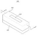
도 1은 본 발명의 일 실시예에 따른 발광소자 어셈블리를 나타내는 사시도이다.
도 2는 도 1의 I-I'를 따라 절단하여 도시한 단면도이다.
도 3은 본 발명의 일 실시예에 따른 발광소자 어셈블리에서 필름 형태의 광학층 및 형광체층을 나타내는 도면이다.
도 4는 본 발명의 다른 실시예에 따른 발광소자 어셈블리를 나타내는 사시도이다.
도 5는 도 4의 II-II'를 따라 절단하여 도시한 단면도이다.
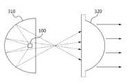
도 6은 본 발명의 일 실시예에 따른 차량용 전조등을 개략적으로 도시한 단면도이다.1 is a perspective view illustrating a light emitting device assembly according to an embodiment of the present invention.
2 is a cross-sectional view taken along line I-I 'of FIG.
3 is a view showing an optical layer and a phosphor layer in the form of a film in a light emitting device assembly according to an embodiment of the present invention.
4 is a perspective view illustrating a light emitting device assembly according to another embodiment of the present invention.
5 is a cross-sectional view taken along line II-II 'of FIG.
6 is a cross-sectional view schematically showing a vehicle headlamp according to an embodiment of the present invention.
본 발명의 설명에 있어서, 각 기판, 층 또는 소자 등이 각 기판, 층 또는 소자 등의 "상(on)"에 또는 "아래(under)"에 형성되는 것으로 기재되는 경우에 있어, "상(on)"과 "아래(under)"는 "직접(directly)" 또는 "다른 구성요소를 개재하여 (indirectly)" 형성되는 것을 모두 포함한다. 또한 각 구성요소의 상 또는 아래에 대한 기준은 도면을 기준으로 설명한다.In the description of the present invention, in the case where each substrate, layer or element is described as being formed "on" or "under" of each substrate, layer or element, quot; on "and" under " include both being formed directly or indirectly through other elements. In addition, the upper or lower reference of each component is described with reference to the drawings.
도면에서의 각 구성요소들의 크기는 설명을 위하여 과장될 수 있으며, 실제로 적용되는 크기를 의미하는 것은 아니다.
The size of each component in the drawings may be exaggerated for the sake of explanation and does not mean the size actually applied.
이하에서는 하기의 도면을 참조하여 본 발명에 따른 발광소자 어셈블리 및 이를 포함하는 전조등을 상세하게 설명한다.
Hereinafter, the light emitting device assembly and the headlamp including the light emitting device assembly according to the present invention will be described in detail with reference to the following drawings.
도 1은 본 발명의 일 실시예에 따른 발광소자 어셈블리를 나타내는 사시도이다. 도 2는 도 1의 I-I'를 따라 절단하여 도시한 단면도이다.1 is a perspective view illustrating a light emitting device assembly according to an embodiment of the present invention. 2 is a cross-sectional view taken along line I-I 'of FIG.
도 1 및 도 2를 참조하면, 본 발명의 일 실시예에 따른 발광소자 어셈블리(100)는, 기판(110), 기판(110)상에 실장되는 적어도 하나의 발광소자 칩(120), 적어도 하나의 발광소자 칩(120)의 측면에 형성되는 제1 반사층(130), 적어도 하나의 발광소자 칩(120) 상에 형성되는 광학층(140), 광학층(140) 상에 형성되는 형광체층(150), 그리고 광학층(140) 및 형광체층(150)의 측면에 형성되는 제2 반사층(160)을 포함한다.
1 and 2, a light
기판(110)은 금속, 실리콘 또는 세라믹으로 제조될 수 있다. 즉, 기판(110)은 유리 또는 사파이어(sapphire)와 같은 물질로 제조된 절연성 기판일 수 있으며, Si, SiC, ZnO와 같은 물질로 제조된 도전성 기판일 수 있다. 기판(110)은 방열 특성이 우수한 재질의 물질로 제조될 수 있다. 기판(110) 상에는 전극(미도시)이 형성될 수 있으며, 이러한 전극은 전기회로를 포함하고 있으며 이를 통해 발광소자 칩(120)에 전원을 인가할 수 있다.
The
기판(110)상에는 광원으로 이용되는 적어도 하나의 발광소자 칩(120)이 실장될 수 있다.At least one light
발광소자 칩(120)에 대해서 간단히 설명하면, 발광소자 칩(120)은 제1 도전형 반도체층, 활성층, 제2 도전형 반도체층 및 전극을 포함할 수 있다. 제1 도전형 반도체층은 n-도핑될 수 있으며, 제1 도전형 반도체층을 통해 전자가 활성층으로 이동된다.The light
제1 도전형 반도체층 상에 활성층이 형성된다. 활성층은 전자와 정공이 재결합하여 발광하도록 양자장벽층과 양자우물층이 교대로 반복된 적층구조로 형성될 수 있다. 활성층은 원하는 발광 파장에 따라 그 조성이 달라질 수 있다.An active layer is formed on the first conductivity type semiconductor layer. The active layer may be formed in a laminated structure in which a quantum barrier layer and a quantum well layer are alternately repeated so that electrons and holes recombine and emit light. The active layer may have a different composition depending on the desired emission wavelength.
활성층 상에 제2 도전형 반도체층이 형성될 수 있다. 제2 도전형 반도체층은 p-도핑될 수 있다. 제2 도전형 반도체층을 통해 정공이 활성층으로 이동된다.And the second conductivity type semiconductor layer may be formed on the active layer. The second conductivity type semiconductor layer may be p-doped. And the holes are transferred to the active layer through the second conductive type semiconductor layer.
제2 도전형 반도체층 상에 투명 전극이 형성될 수 있다. 투명 전극은 Ni/Au와 같은 투명 금속층으로 형성되거나, ITO와 같은 전도성 산화물로 형성될 수 있다. 투명 전극 상에 p형 전극이 형성되고, 제1 도전형 반도체층 상에 n형 전극이 형성된다. p형 전극 및 n형 전극은 Ti/Al 등 다양한 금속 재료로 형성될 수 있다.A transparent electrode may be formed on the second conductivity type semiconductor layer. The transparent electrode may be formed of a transparent metal layer such as Ni / Au, or may be formed of a conductive oxide such as ITO. A p-type electrode is formed on the transparent electrode, and an n-type electrode is formed on the first conductivity type semiconductor layer. The p-type electrode and the n-type electrode may be formed of various metal materials such as Ti / Al.
p형 전극을 통해 정공이 공급되며, n형 전극을 통해 전자가 공급된다. 이렇게 공급된 정공 및 전자는 활성층에서 결합함으로써 빛 에너지를 발생시킨다. 방출되는 빛의 파장에 따라 자외선 발광소자 또는 청색 발광소자일 수 있다.
holes are supplied through the p-type electrode, and electrons are supplied through the n-type electrode. The holes and electrons thus supplied are combined in the active layer to generate light energy. And may be an ultraviolet light emitting element or a blue light emitting element depending on the wavelength of emitted light.
적어도 하나의 발광소자 칩(120)의 측면에 제1 반사층(130)이 형성될 수 있다. 즉, 제1 반사층(130)은 발광소자 칩(120)의 사이사이에 형성될 수 있다. 제1 반사층(130)은 복수개의 발광소자 칩(120) 사이의 공간에서 발생되는 암부를 개선하기 위해 형성될 수 있다. 결국, 제1 반사층(130)이 발광소자 칩(120) 사이의 공간에 충진됨으로써 각각의 발광소자 칩(120) 부분보다 발광소자 칩(120) 사이사이에서 상대적으로 휘도가 떨어지는 암부의 발생을 개선시킬 수 있다.The first
제1 반사층(130)은 발광소자 칩(120)의 측면에서 나오는 빛을 반사시켜 광학층(140)으로 전달시킬 수 있다.
The first
광학층(140)은 적어도 하나의 발광소자 칩(120) 상에 형성될 수 있다. 또한, 광학층(140)은 복수개의 발광소자 칩(120) 사이에 형성된 제1 반사층(130) 상에 형성될 수 있다. 즉, 광학층(140)은 각각의 발광소자 칩(120)마다 형성되는 것이 아니라, 복수개의 발광소자 칩(120) 전면에 걸쳐서 형성될 수 있다. 이로 인해, 발광소자 칩(120)의 상부에서 발생된 광 뿐만 아니라 발광소자 칩(120)의 측면에서 발생되어 제1 반사층(130)에 의해 전달된 광 모두가 광학층(140)을 통해 형광체층(150)에 전달될 수 있다.The
광학층(140)은 발광소자 칩(120)으로부터 발생된 빛을 형광체층(150)으로 전달하는 도광판 역할을 한다. 발광소자 칩(120)과 형광체층(150) 사이에 투명한 물질로 형성된 광학층(140)이 배치됨으로써 발광소자 칩(120)과 형광체층(150)이 직접 맞닿아 있지 않도록 하여 광 손실을 줄일 수 있다.The
광학층(140)은 투명한 물질로 형성될 수 있다. 광학층(140)은 실리콘(silicone)으로 형성될 수 있다. 즉, 광학층(140)은 빛의 투과율이 90% 이상인 실리콘 레진으로 형성될 수 있으며, 예를 들어 광학층(140)은 투명 실리콘 수지 조성물, 에폭시 수지 및 변성 에폭시 수지 조성물 중에서 선택된 적어도 하나의 물질로 형성될 수 있으나, 이에 제한되지 않는다. 또한, 광학층(140)은 유리와 같은 투명한 재질 또는 플라스틱 합성 수지의 절연 조성물로 형성될 수 있다.The
본 발명의 일 측에 따른 발광소자 어셈블리에서, 광학층(140)은 산란 입자를 포함할 수 있으며, 산란 입자는 이산화규소(SiO2)일 수 있다. 광학층(140)에 산란 입자가 포함됨으로써 발광소자 칩(120)으로부터 전달된 빛을 산란시켜 광 추출 효율을 향상시킬 수 있다. 또한, 본 발명의 일 측에 따른 발광소자 어셈블리에서, 광학층(140)의 상부는 패터닝될 수 있다. 광학층(140)의 상부가 미세 요철 형상으로 패터닝되어 광학층(140) 내부로 손실되는 빛의 양을 줄임으로써 광 추출 효율을 증가시킬 수 있다.
In the light emitting device assembly according to one side of the present invention, an
형광체층(150)은 광학층(140) 상에 형성될 수 있다. 발광소자 칩(120)으로부터 나온 빛은 광학층(140)을 통해 전달되고, 형광체층(150)을 통과하여 외부로 나아갈 수 있다.The
형광체층(150)은 발광소자 칩(120)에서 나온 빛을 스캐터링하여 색변환을 할 수 있다. 예를 들어, 발광소자 칩(120)으로부터 나온 청색 빛이 형광체층(150)을 통과하면서 황색, 녹색 또는 적색으로 변환되어 백색광이 외부로 방출될 수 있다.The
형광체층(150)은 청색광을 황색, 녹색 또는 빨강으로 변환시킬 수 있는 형광물질을 포함할 수 있다. 형광체층(150)은 호스트 물질과 활성물질을 포함할 수 있으며, 예를 들어 이트륨 알루미늄 가넷(YAG)의 호스트 물질에 세륨(Ce) 활성물질을 포함할 수 있다. 또한, 형광체층(150)은 실리케이트 계열의 호스트 물질에 유로피움(Eu) 활성물질을 사용할 수 있으나, 이에 제한되지 않는다.The
형광체층(150)은 얇고 균일한 두께로 형성될 수 있다. 형광체층(150)에는 형광체 입자가 균일하게 분산되어 있을 수 있다. 따라서, 형광체층(150)을 통과하는 빛은 균일하게 색변환될 수 있다.
The
도 3은 본 발명의 일 실시예에 따른 발광소자 어셈블리에서 필름 형태의 광학층(140) 및 형광체층(150)을 나타내는 도면이다. 더욱 상세하게는, 도 3a는 광학층(140) 및 형광체층(150)이 필름형으로 개별적으로 제작된 것을 나타내며, 도 3b는 광학층(140) 및 형광체층(150)이 일체로 된 필름형으로 제작된 것을 나타내는 도면이다.3 is a view showing an
본 발명의 일 측에 따른 발광소자 어셈블리에서, 광학층(140) 및 형광체층(150)은 필름형으로 제작되어 적어도 하나의 발광소자 칩(120) 상에 적층될 수 있다. 도 3a에서와 같이 광학층(140) 및 형광체층(150)은 필름형으로 개별적으로 제작되어, 순차적으로 적어도 하나의 발광소자 칩(120) 상에 적층될 수 있다. 나아가, 도 3b에서와 같이 광학층(140) 및 형광체층(150)은 일체로 된 필름형으로 제작되어, 하나의 공정으로 적어도 하나의 발광소자 칩(120) 상에 적층될 수 있다. 따라서, 광학층(140) 및 형광체층(150)은 필름형으로 미리 제작되어 제조공정을 단순화시킬 수 있다.In the light emitting device assembly according to one aspect of the present invention, the
이와 달리, 광학층(140) 및 형광체층(150)은 액상의 물질을 적어도 하나의 발광소자 칩(120) 및 제1 반사층(130) 상에 도포한 후 열경화 또는 UV 경화를 사용하여 형성될 수 있다.
Alternatively, the
제2 반사층(160)은 광원부의 경계에서 명암비를 확보하고 전광속을 향상시키기 위해 광학층(140) 및 형광체층(150)의 측면에 형성될 수 있다. 또한, 제1 반사층(130)이 적어도 하나의 발광소자 칩(120) 사이에만 형성된 경우, 제2 반사층(160)은 최외각의 발광소자 칩(120)의 측면에도 형성될 수 있다. 즉, 최외각의 발광소자 칩(120)의 측면에는 제1 반사층(130) 또는 제2 반사층(160)이 형성될 수 있다.The second
결국, 발광소자 칩(120), 광학층(140) 및 형광체층(150)의 측면에 반사층이 형성됨으로써 광원의 높은 명암비를 확보할 수 있다. 본 발명의 일 측에 따른 발광소자 어셈블리에서, 제1 반사층(130) 및 제2 반사층(160)은 동일한 물질로 형성될 수 있다. 제1 반사층(130) 및 제2 반사층(160)은 광 반사성 재료인 Ti, Zr, Nb, Al, Si로 이루어진 그룹으로부터 선택되는 1종의 산화물, AlN, 또는 MgF 중 적어도 1종의 물질로 형성될 수 있다. 예를 들어, 제1 반사층(130) 및 제2 반사층(160)은 이산화티탄(TiO2), 이산화지르코늄(Zr2O), 오산화니오븀(Nb2O5), 산화알루미늄(Al2O3), 플루오르화마그네슘(MgF), 질화알루미늄(AlN) 및 이산화규소(SiO2)로 이루어진 그룹으로부터 선택될 수 있다.
As a result, the reflective layer is formed on the side surfaces of the light emitting
결국, 본 발명의 일 실시예에 따른 발광소자 어셈블리는 형광체층(150)을 통해서만 외부로 빛이 방출되고, 이를 제외한 영역에서는 제2 반사층(160)으로 인해 빛이 발산되지 않음으로써 명암비를 높일 수 있다. 또한, 명암비를 높이기 위한 별도의 쉴드 구조를 생략할 수 있으므로 광 손실을 최소화하여 광 추출 효율을 향상시킬 수 있다.
As a result, in the light emitting device assembly according to an embodiment of the present invention, light is emitted only to the outside through the
이하에서는 중복된 설명을 피하기 위해, 도 1 및 도 2와 상이한 부분에 대해서 상세히 설명하기로 한다.
Hereinafter, in order to avoid redundant description, portions different from FIG. 1 and FIG. 2 will be described in detail.
도 4는 본 발명의 다른 실시예에 따른 발광소자 어셈블리를 나타내는 사시도이다. 도 5는 도 4의 II-II'를 따라 절단하여 도시한 단면도이다.
4 is a perspective view illustrating a light emitting device assembly according to another embodiment of the present invention. 5 is a cross-sectional view taken along line II-II 'of FIG.
도 4 및 도 5를 참조하면, 본 발명의 다른 실시예에 따른 발광소자 어셈블리(200)는, 기판(110), 기판(110)상에 실장되는 적어도 하나의 발광소자 칩(120), 적어도 하나의 발광소자 칩(120)의 측면에 형성되는 제1 반사층(130), 적어도 하나의 발광소자 칩(120) 상에 형성되며, 산란 입자를 포함하는 형광체층(150) 및 형광체층(150)의 측면에 형성되는 제2 반사층(160)을 포함한다.
4 and 5, a light emitting
형광체층(150)이 발광소자 칩(120) 상에 바로 형성되어 있으며, 산란 입자를 포함할 수 있다. 형광체층(150)이 발광소자 칩(120)과 맞닿아 있는 경우, 발광소자 내부에서 손실되는 광이 많아 광 추출 효율이 낮아질 수 있으나, 본 발명에서는 형광체층(150)에 산란 입자가 포함됨으로써 광 추출 효율이 낮아지는 것을 방지할 수 있다.The
형광체층(150)에 포함된 산란 입자는 이산화규소(SiO2)일 수 있다. 즉, 형광체층(150)에 산란 입자가 포함됨으로써 발광소자 칩(120)으로부터 전달된 빛을 산란시켜 광 추출 효율을 향상시킬 수 있다. 또한, 본 발명의 일 측에 따른 발광소자 어셈블리에서, 형광체층(150)의 상부는 패터닝될 수 있다. 형광체층(150)의 상부가 미세 요철 형상으로 패터닝되어 발광소자 내부로 손실되는 빛의 양을 줄임으로써 광 추출 효율을 증가시킬 수 있다.
The scattering particles contained in the
상술한 바와 같이, 제1 반사층(130) 및 제2 반사층(160)은 광 반사성 재료인 Ti, Zr, Nb, Al, Si로 이루어진 그룹으로부터 선택되는 1종의 산화물, AlN, 또는 MgF 중 적어도 1종의 물질로 형성될 수 있다. 예를 들어, 제1 반사층(130) 및 제2 반사층(160)은 이산화티탄(TiO2), 이산화지르코늄(Zr2O), 오산화니오븀(Nb2O5), 산화알루미늄(Al2O3), 플루오르화마그네슘(MgF), 질화알루미늄(AlN) 및 이산화규소(SiO2)로 이루어진 그룹으로부터 선택될 수 있다.As described above, the first
산란 입자를 포함하는 형광체층(150)은 필름형으로 제작되어 적어도 하나의 발광소자 칩(120) 상에 적층될 수 있다. 따라서, 산란 입자를 포함하는 형광체층(150)이 필름형으로 미리 제작된 후 발광소자 칩(120) 상에 적층되므로 제조공정을 단순화시킬 수 있다.
The
도 6은 본 발명의 일 실시예에 따른 차량용 전조등을 개략적으로 도시한 단면도이다.
6 is a cross-sectional view schematically showing a vehicle headlamp according to an embodiment of the present invention.
본 발명의 일 실시예에 따른 발광소자 어셈블리를 포함하는 전조등은, 상술한 바와 같은 발광소자 어셈블리(100), 리플렉터(310) 및 렌즈(320)를 포함한다.The headlamp including the light emitting device assembly according to an embodiment of the present invention includes the light emitting
리플렉터(310)는 발광소자 어셈블리(100)에 의해 생성된 광을 차량의 전방으로 반사하도록 구비될 수 있으며, 이를 위해 특정 형상으로 형성될 수 있다. 더욱 상세하게는, 리플렉터(310)는 다양한 구조로 형성될 수 있으며, 예를 들어 포물선형, 직선형 또는 옵티컬형 리플렉터 구조로 제작될 수 있다.The
렌즈(320)는 리플렉터(310)에 의해 반사되어 차량의 전방으로 조사되는 광을 투사할 수 있다. 렌즈(320)는 비구면 렌즈일 수 있으나, 이제 제한되지 않는다.
The
따라서, 본 발명의 실시예들에 따른 발광소자 어셈블리는 적어도 하나의 발광소자 칩 사이의 암부를 개선시키고, 빛의 손실을 줄이면서 높은 명암비를 확보할 수 있다. 또한, 본 발명의 실시예들에 따른 발광소자 어셈블리는 쉴드 구조를 생략할 수 있으며, 이에 따라 단순한 구조로 차량용 전조등을 제작할 수 있다.
Therefore, the light emitting device assembly according to the embodiments of the present invention can improve the dark area between at least one light emitting device chip, and can secure a high contrast ratio while reducing light loss. In addition, the light emitting device assembly according to the embodiments of the present invention can omit the shield structure, and thus a vehicle headlamp can be manufactured with a simple structure.
이상에서 실시예를 중심으로 설명하였으나 이는 단지 예시일 뿐 본 발명을 한정하는 것이 아니며, 본 발명이 속하는 분야의 통상의 지식을 가진 자라면 본 실시예의 본질적인 특성을 벗어나지 않는 범위에서 이상에 예시되지 않은 여러 가지의 변형과 응용이 가능함을 알 수 있을 것이다. 예를 들어, 실시예에 구체적으로 나타난 각 구성요소는 변형하여 실시할 수 있는 것이다. 그리고 이러한 변형과 응용에 관계된 차이점들은 첨부된 청구 범위에서 규정하는 본 발명의 범위에 포함되는 것으로 해석되어야 할 것이다.
While the present invention has been particularly shown and described with reference to exemplary embodiments thereof, it is to be understood that the invention is not limited to the disclosed exemplary embodiments, but, on the contrary, It will be understood that various modifications and applications are possible. For example, each component specifically shown in the embodiments can be modified and implemented. It is to be understood that all changes and modifications that come within the meaning and range of equivalency of the claims are therefore intended to be embraced therein.
110 : 기판120 : 발광소자 칩
130 : 제1 반사층140 : 광학층
150 : 형광체층160 : 제2 반사층
310 : 리플렉터320 : 렌즈110: substrate 120: light emitting device chip
130: first reflecting layer 140: optical layer
150: phosphor layer 160: second reflective layer
310: Reflector 320: Lens
Claims (15)
Translated fromKorean상기 기판 상에 실장되는 복수의 발광소자 칩;
상기 복수의 발광소자 칩의 측면에서, 상기 복수의 발광소자 칩 사이를 매립하도록 배치되는 제1 반사층;
상기 복수의 발광소자 칩 및 상기 제1 반사층의 상면 상에 배치되는 광학층;
상기 광학층 상에 배치되는 형광체층; 및
상기 광학층 및 상기 형광체층의 측면에 배치되는 제2 반사층;
을 포함하는 발광소자 어셈블리.
Board;
A plurality of light emitting device chips mounted on the substrate;
A first reflective layer disposed on a side surface of the plurality of light emitting device chips, the first reflective layer being disposed between the plurality of light emitting device chips;
An optical layer disposed on an upper surface of the plurality of light emitting device chips and the first reflective layer;
A phosphor layer disposed on the optical layer; And
A second reflective layer disposed on a side surface of the optical layer and the phosphor layer;
And a light emitting diode.
상기 광학층은 투명한 물질로 형성되는 발광소자 어셈블리.
The method according to claim 1,
Wherein the optical layer is formed of a transparent material.
상기 광학층은 실리콘(silicone)으로 형성되는 발광소자 어셈블리.
3. The method of claim 2,
Wherein the optical layer is formed of silicone.
상기 광학층은 산란 입자를 포함하는 발광소자 어셈블리.
The method according to claim 1,
Wherein the optical layer includes scattering particles.
상기 광학층의 상부는 패터닝되어 있는 발광소자 어셈블리.
The method according to claim 1,
And an upper portion of the optical layer is patterned.
상기 제1 반사층 및 상기 제2 반사층은 동일한 물질로 형성되는 발광소자 어셈블리.
The method according to claim 1,
Wherein the first reflective layer and the second reflective layer are formed of the same material.
상기 제1 반사층 및 상기 제2 반사층 중 적어도 하나는, 이산화티탄(TiO2), 이산화지르코늄(Zr2O), 오산화니오븀(Nb2O5), 산화알루미늄(Al2O3), 플루오르화마그네슘(MgF), 질화알루미늄(AlN) 및 이산화규소(SiO2)로 이루어진 그룹으로부터 선택되는 물질을 포함하는 발광소자 어셈블리.
7. The method according to claim 1 or 6,
Wherein at least one of the first reflective layer and the second reflective layer is formed of at least one selected from the group consisting of TiO2 , Zr2 O, Nb2 O5 , Al2 O3 , (MgF 2), aluminum nitride (AlN), and silicon dioxide (SiO2 ).
상기 광학층 및 상기 형광체층은 필름형으로 제작되어 상기 복수의 발광소자 칩 상에 적층되는 발광소자 어셈블리.
The method according to claim 1,
Wherein the optical layer and the phosphor layer are formed in a film shape and stacked on the plurality of light emitting device chips.
상기 기판 상에 실장되는 복수의 발광소자 칩;
상기 복수의 발광소자 칩의 측면에서, 상기 복수의 발광소자 칩 사이를 매립하도록 배치되는 제1 반사층;
상기 복수의 발광소자 칩 및 상기 제1 반사층의 상면 상에 배치되며, 산란 입자를 포함하는 형광체층; 및
상기 형광체층의 측면에 배치되는 제2 반사층;
을 포함하는 발광소자 어셈블리.
Board;
A plurality of light emitting device chips mounted on the substrate;
A first reflective layer disposed on a side surface of the plurality of light emitting device chips, the first reflective layer being disposed between the plurality of light emitting device chips;
A phosphor layer disposed on the upper surface of the plurality of light emitting device chips and the first reflective layer and including scattering particles; And
A second reflective layer disposed on a side surface of the phosphor layer;
And a light emitting diode.
상기 발광소자 어셈블리에 의해 생성된 광을 차량의 전방으로 반사하는 리플렉터; 및
상기 리플렉터에 의해 반사되어 차량의 전방으로 조사되는 광을 투사하는 렌즈;
를 포함하는 차량용 전조등.A light emitting device assembly according to any one of claims 1 to 9;
A reflector for reflecting the light generated by the light emitting device assembly toward the front of the vehicle; And
A lens for reflecting light reflected by the reflector and irradiated to the front of the vehicle;
And a headlight for a vehicle.
Priority Applications (6)
| Application Number | Priority Date | Filing Date | Title |
|---|---|---|---|
| KR1020110046845AKR101798884B1 (en) | 2011-05-18 | 2011-05-18 | Light emitting device assembly and head light including the same |
| EP12167043.4AEP2525418A3 (en) | 2011-05-18 | 2012-05-08 | Light emitting device assembly and headlamp including the same |
| TW101116805ATWI558944B (en) | 2011-05-18 | 2012-05-11 | Illuminating device assembly and pre-lighting device including the same |
| US13/475,486US8882319B2 (en) | 2011-05-18 | 2012-05-18 | Light emitting device assembly and headlamp including the same |
| US14/151,733US8921883B2 (en) | 2011-05-18 | 2014-01-09 | Light emitting device assembly and headlamp including the same |
| US14/575,741US9188300B2 (en) | 2011-05-18 | 2014-12-18 | Light emitting device assembly and headlamp including the same |
Applications Claiming Priority (1)
| Application Number | Priority Date | Filing Date | Title |
|---|---|---|---|
| KR1020110046845AKR101798884B1 (en) | 2011-05-18 | 2011-05-18 | Light emitting device assembly and head light including the same |
Publications (2)
| Publication Number | Publication Date |
|---|---|
| KR20120128909A KR20120128909A (en) | 2012-11-28 |
| KR101798884B1true KR101798884B1 (en) | 2017-11-17 |
Family
ID=46125194
Family Applications (1)
| Application Number | Title | Priority Date | Filing Date |
|---|---|---|---|
| KR1020110046845AActiveKR101798884B1 (en) | 2011-05-18 | 2011-05-18 | Light emitting device assembly and head light including the same |
Country Status (4)
| Country | Link |
|---|---|
| US (3) | US8882319B2 (en) |
| EP (1) | EP2525418A3 (en) |
| KR (1) | KR101798884B1 (en) |
| TW (1) | TWI558944B (en) |
Families Citing this family (12)
| Publication number | Priority date | Publication date | Assignee | Title |
|---|---|---|---|---|
| US10696210B2 (en)* | 2013-02-25 | 2020-06-30 | Rensselaer Polytechnic Institute | Low luminance lighting |
| KR20140115841A (en) | 2013-03-22 | 2014-10-01 | 삼성디스플레이 주식회사 | Lighting apparatus and lighting unit |
| DE102013205836A1 (en)* | 2013-04-03 | 2014-10-09 | Osram Opto Semiconductors Gmbh | vehicle light |
| JP6307703B2 (en)* | 2013-05-31 | 2018-04-11 | パナソニックIpマネジメント株式会社 | Wavelength converting element, light emitting device including wavelength converting element, vehicle including light emitting device, and method of manufacturing wavelength converting element |
| KR102089571B1 (en)* | 2013-07-25 | 2020-03-16 | 현대모비스 주식회사 | Lamp for Vehicle |
| KR102075993B1 (en)* | 2013-12-23 | 2020-02-11 | 삼성전자주식회사 | Method of Fabricating White LED Devices |
| CN105431953B (en)* | 2014-06-05 | 2018-03-16 | 上海富迪照明电器有限公司 | Embedded white light LED packaging structure and manufacturing method based on solid-state fluorescent material |
| DE102015219799A1 (en)* | 2015-10-13 | 2017-04-27 | Osram Gmbh | Conversion device and vehicle headlights |
| JP6332294B2 (en)* | 2015-11-30 | 2018-05-30 | 日亜化学工業株式会社 | Light emitting device |
| US10797209B2 (en)* | 2016-02-05 | 2020-10-06 | Maven Optronics Co., Ltd. | Light emitting device with beam shaping structure and manufacturing method of the same |
| US20200263846A1 (en)* | 2019-02-20 | 2020-08-20 | Magna Closures Inc. | Vehicle light assembly with quantum doped material illuminable using distinct illumination sources |
| EP4012507A1 (en)* | 2020-12-11 | 2022-06-15 | The Swatch Group Research and Development Ltd | Phosphorescent timepiece component |
Citations (3)
| Publication number | Priority date | Publication date | Assignee | Title |
|---|---|---|---|---|
| US20070012940A1 (en) | 2005-07-14 | 2007-01-18 | Samsung Electro-Mechanics Co., Ltd. | Wavelength-convertible light emitting diode package |
| WO2010106478A1 (en)* | 2009-03-19 | 2010-09-23 | Koninklijke Philips Electronics N.V. | Color adjusting arrangement |
| US20110062469A1 (en) | 2009-09-17 | 2011-03-17 | Koninklijke Philips Electronics N.V. | Molded lens incorporating a window element |
Family Cites Families (45)
| Publication number | Priority date | Publication date | Assignee | Title |
|---|---|---|---|---|
| CN1143394C (en) | 1996-08-27 | 2004-03-24 | 精工爱普生株式会社 | Peeling method, thin film device transfer method and thin film device |
| USRE38466E1 (en) | 1996-11-12 | 2004-03-16 | Seiko Epson Corporation | Manufacturing method of active matrix substrate, active matrix substrate and liquid crystal display device |
| US7208725B2 (en) | 1998-11-25 | 2007-04-24 | Rohm And Haas Electronic Materials Llc | Optoelectronic component with encapsulant |
| JP3906654B2 (en) | 2000-07-18 | 2007-04-18 | ソニー株式会社 | Semiconductor light emitting device and semiconductor light emitting device |
| US7129638B2 (en)* | 2000-08-09 | 2006-10-31 | Avago Technologies General Ip (Singapore) Pte. Ltd. | Light emitting devices with a phosphor coating having evenly dispersed phosphor particles and constant thickness |
| US6818465B2 (en) | 2001-08-22 | 2004-11-16 | Sony Corporation | Nitride semiconductor element and production method for nitride semiconductor element |
| JP2003218034A (en) | 2002-01-17 | 2003-07-31 | Sony Corp | Selective growth method, semiconductor light emitting device and method of manufacturing the same |
| JP3815335B2 (en) | 2002-01-18 | 2006-08-30 | ソニー株式会社 | Semiconductor light emitting device and manufacturing method thereof |
| JP4172196B2 (en)* | 2002-04-05 | 2008-10-29 | 豊田合成株式会社 | Light emitting diode |
| KR100499129B1 (en) | 2002-09-02 | 2005-07-04 | 삼성전기주식회사 | Light emitting laser diode and fabricatin method thereof |
| US7002182B2 (en) | 2002-09-06 | 2006-02-21 | Sony Corporation | Semiconductor light emitting device integral type semiconductor light emitting unit image display unit and illuminating unit |
| JP2004127662A (en)* | 2002-10-01 | 2004-04-22 | Sony Corp | Display device |
| US6917057B2 (en) | 2002-12-31 | 2005-07-12 | Gelcore Llc | Layered phosphor coatings for LED devices |
| KR100714639B1 (en) | 2003-10-21 | 2007-05-07 | 삼성전기주식회사 | Light emitting element |
| KR100506740B1 (en) | 2003-12-23 | 2005-08-08 | 삼성전기주식회사 | Nitride semiconductor light emitting device and method of manufacturing the same |
| US7517728B2 (en)* | 2004-03-31 | 2009-04-14 | Cree, Inc. | Semiconductor light emitting devices including a luminescent conversion element |
| DE102005030128B4 (en)* | 2004-06-28 | 2011-02-03 | Kyocera Corp. | Light-emitting device and lighting device |
| JP2006114854A (en)* | 2004-10-18 | 2006-04-27 | Sharp Corp | Backlight device for semiconductor light emitting device and liquid crystal display device |
| KR100664985B1 (en) | 2004-10-26 | 2007-01-09 | 삼성전기주식회사 | Nitride-based semiconductor device |
| KR100624448B1 (en)* | 2004-12-02 | 2006-09-18 | 삼성전기주식회사 | Semiconductor light emitting device and manufacturing method thereof |
| TWI237411B (en)* | 2004-12-06 | 2005-08-01 | Internat Semiconductor Technol | Process and structure for packaging LED's |
| KR100665222B1 (en) | 2005-07-26 | 2007-01-09 | 삼성전기주식회사 | LED package using diffusion material and manufacturing method thereof |
| WO2007018039A1 (en)* | 2005-08-05 | 2007-02-15 | Matsushita Electric Industrial Co., Ltd. | Semiconductor light-emitting device |
| JP4579094B2 (en) | 2005-08-23 | 2010-11-10 | 株式会社小糸製作所 | Vehicle headlamp |
| KR100661614B1 (en) | 2005-10-07 | 2006-12-26 | 삼성전기주식회사 | Nitride-based semiconductor light emitting device and its manufacturing method |
| KR100723247B1 (en) | 2006-01-10 | 2007-05-29 | 삼성전기주식회사 | Chip coated LED package and manufacturing method thereof |
| KR100735325B1 (en) | 2006-04-17 | 2007-07-04 | 삼성전기주식회사 | Light emitting diode package and its manufacturing method |
| TWM309750U (en)* | 2006-10-18 | 2007-04-11 | Lighthouse Technology Co Ltd | Light emitting diode package |
| KR100930171B1 (en) | 2006-12-05 | 2009-12-07 | 삼성전기주식회사 | White light emitting device and white light source module using same |
| KR100855065B1 (en) | 2007-04-24 | 2008-08-29 | 삼성전기주식회사 | Light emitting diode package |
| KR100982980B1 (en) | 2007-05-15 | 2010-09-17 | 삼성엘이디 주식회사 | Surface light source device and LCD backlight unit having same |
| KR101164026B1 (en) | 2007-07-12 | 2012-07-18 | 삼성전자주식회사 | Nitride semiconductor light emitting device and fabrication method thereof |
| TWM334470U (en)* | 2007-08-14 | 2008-06-11 | Wellypower Optronics Corp | Light emitting diode device |
| KR100891761B1 (en) | 2007-10-19 | 2009-04-07 | 삼성전기주식회사 | Semiconductor light emitting device, manufacturing method thereof and semiconductor light emitting device package using same |
| CN101487581A (en)* | 2008-01-17 | 2009-07-22 | 富士迈半导体精密工业(上海)有限公司 | LED light source module |
| KR101332794B1 (en) | 2008-08-05 | 2013-11-25 | 삼성전자주식회사 | Light emitting device, light emitting system comprising the same, and fabricating method of the light emitting device and the light emitting system |
| KR20100030470A (en) | 2008-09-10 | 2010-03-18 | 삼성전자주식회사 | Light emitting device and system providing white light with various color temperatures |
| KR101530876B1 (en) | 2008-09-16 | 2015-06-23 | 삼성전자 주식회사 | Light emitting device with increased light emitting amount, light emitting device including same, method of manufacturing light emitting device and light emitting device |
| US8008683B2 (en) | 2008-10-22 | 2011-08-30 | Samsung Led Co., Ltd. | Semiconductor light emitting device |
| JP5326705B2 (en)* | 2009-03-17 | 2013-10-30 | 日亜化学工業株式会社 | Light emitting device |
| JP5482378B2 (en)* | 2009-04-20 | 2014-05-07 | 日亜化学工業株式会社 | Light emitting device |
| JP5326837B2 (en)* | 2009-06-08 | 2013-10-30 | 日亜化学工業株式会社 | Light emitting device |
| KR101094251B1 (en)* | 2009-09-30 | 2011-12-19 | 허재원 | LED module illuminated from all directions |
| JP4919179B2 (en)* | 2010-05-11 | 2012-04-18 | 独立行政法人電子航法研究所 | Millimeter wave radar built-in headlamp |
| TWM397595U (en)* | 2010-08-05 | 2011-02-01 | Unity Opto Technology Co Ltd | LED structure |
- 2011
- 2011-05-18KRKR1020110046845Apatent/KR101798884B1/enactiveActive
- 2012
- 2012-05-08EPEP12167043.4Apatent/EP2525418A3/ennot_activeWithdrawn
- 2012-05-11TWTW101116805Apatent/TWI558944B/enactive
- 2012-05-18USUS13/475,486patent/US8882319B2/enactiveActive
- 2014
- 2014-01-09USUS14/151,733patent/US8921883B2/enactiveActive
- 2014-12-18USUS14/575,741patent/US9188300B2/enactiveActive
Patent Citations (3)
| Publication number | Priority date | Publication date | Assignee | Title |
|---|---|---|---|---|
| US20070012940A1 (en) | 2005-07-14 | 2007-01-18 | Samsung Electro-Mechanics Co., Ltd. | Wavelength-convertible light emitting diode package |
| WO2010106478A1 (en)* | 2009-03-19 | 2010-09-23 | Koninklijke Philips Electronics N.V. | Color adjusting arrangement |
| US20110062469A1 (en) | 2009-09-17 | 2011-03-17 | Koninklijke Philips Electronics N.V. | Molded lens incorporating a window element |
Also Published As
| Publication number | Publication date |
|---|---|
| EP2525418A2 (en) | 2012-11-21 |
| EP2525418A3 (en) | 2016-05-18 |
| US8882319B2 (en) | 2014-11-11 |
| TW201250152A (en) | 2012-12-16 |
| US20150103547A1 (en) | 2015-04-16 |
| KR20120128909A (en) | 2012-11-28 |
| US9188300B2 (en) | 2015-11-17 |
| US20120294025A1 (en) | 2012-11-22 |
| US20140124815A1 (en) | 2014-05-08 |
| TWI558944B (en) | 2016-11-21 |
| US8921883B2 (en) | 2014-12-30 |
Similar Documents
| Publication | Publication Date | Title |
|---|---|---|
| KR101798884B1 (en) | Light emitting device assembly and head light including the same | |
| CN103392093B (en) | Light emitting module and lamps apparatus for vehicle | |
| US7581860B2 (en) | Headlight and headlight element | |
| JP5059208B2 (en) | Lighting device and vehicle headlamp | |
| CN102563485B (en) | Light emitting device, vehicle headlamp, lighting device, and vehicle | |
| EP2016629B1 (en) | Vehicle headlight | |
| JP4796031B2 (en) | Vehicle headlight light source and vehicle headlight | |
| KR101227582B1 (en) | Led array | |
| US9970605B2 (en) | Semiconductor light source apparatus | |
| JP6965047B2 (en) | Automotive lighting and / or signaling equipment | |
| JP2011009305A (en) | Light-emitting module | |
| JP2015149307A (en) | Light emitting module and vehicle lamp fitting | |
| KR20190132124A (en) | Lighting module and lighting apparatus | |
| CN106545812A (en) | Light source module and the illuminator with light source module | |
| JP2012099282A (en) | Lighting system and headlight for vehicle | |
| US20120098017A1 (en) | Light emitting module, method of producing light-emitting module, and lighting fixture unit | |
| US20150108523A1 (en) | Semiconductor light-emitting device | |
| KR102677646B1 (en) | Light emitting device package and lighting device | |
| JP2020025063A (en) | Light emitting device and method of manufacturing the same | |
| JP2009070892A (en) | Led light source | |
| JP2010219163A (en) | Light emitting module and lamp fitting unit | |
| CN109751564B (en) | Phosphor module | |
| US20120008306A1 (en) | Light emitting module and lamp unit | |
| JP2012199078A (en) | Light-emitting device, illumination device, headlight for vehicle, and method for manufacturing light-emitting part | |
| KR20200126290A (en) | Lighting module and lighting apparatus |
Legal Events
| Date | Code | Title | Description |
|---|---|---|---|
| PA0109 | Patent application | Patent event code:PA01091R01D Comment text:Patent Application Patent event date:20110518 | |
| N231 | Notification of change of applicant | ||
| PN2301 | Change of applicant | Patent event date:20120704 Comment text:Notification of Change of Applicant Patent event code:PN23011R01D | |
| PG1501 | Laying open of application | ||
| A201 | Request for examination | ||
| PA0201 | Request for examination | Patent event code:PA02012R01D Patent event date:20160517 Comment text:Request for Examination of Application Patent event code:PA02011R01I Patent event date:20110518 Comment text:Patent Application | |
| E902 | Notification of reason for refusal | ||
| PE0902 | Notice of grounds for rejection | Comment text:Notification of reason for refusal Patent event date:20170616 Patent event code:PE09021S01D | |
| E701 | Decision to grant or registration of patent right | ||
| PE0701 | Decision of registration | Patent event code:PE07011S01D Comment text:Decision to Grant Registration Patent event date:20171108 | |
| GRNT | Written decision to grant | ||
| PR0701 | Registration of establishment | Comment text:Registration of Establishment Patent event date:20171113 Patent event code:PR07011E01D | |
| PR1002 | Payment of registration fee | Payment date:20171114 End annual number:3 Start annual number:1 | |
| PG1601 | Publication of registration | ||
| PR1001 | Payment of annual fee | Payment date:20211027 Start annual number:5 End annual number:5 | |
| PR1001 | Payment of annual fee | Payment date:20241024 Start annual number:8 End annual number:8 |