KR101796656B1 - Vertical inline cvd system - Google Patents
Vertical inline cvd systemDownload PDFInfo
- Publication number
- KR101796656B1 KR101796656B1KR1020127031556AKR20127031556AKR101796656B1KR 101796656 B1KR101796656 B1KR 101796656B1KR 1020127031556 AKR1020127031556 AKR 1020127031556AKR 20127031556 AKR20127031556 AKR 20127031556AKR 101796656 B1KR101796656 B1KR 101796656B1
- Authority
- KR
- South Korea
- Prior art keywords
- chamber body
- coupled
- substrates
- processing
- plasma
- Prior art date
- Legal status (The legal status is an assumption and is not a legal conclusion. Google has not performed a legal analysis and makes no representation as to the accuracy of the status listed.)
- Expired - Fee Related
Links
Images


Classifications
- H—ELECTRICITY
- H01—ELECTRIC ELEMENTS
- H01L—SEMICONDUCTOR DEVICES NOT COVERED BY CLASS H10
- H01L21/00—Processes or apparatus adapted for the manufacture or treatment of semiconductor or solid state devices or of parts thereof
- H01L21/67—Apparatus specially adapted for handling semiconductor or electric solid state devices during manufacture or treatment thereof; Apparatus specially adapted for handling wafers during manufacture or treatment of semiconductor or electric solid state devices or components ; Apparatus not specifically provided for elsewhere
- H01L21/677—Apparatus specially adapted for handling semiconductor or electric solid state devices during manufacture or treatment thereof; Apparatus specially adapted for handling wafers during manufacture or treatment of semiconductor or electric solid state devices or components ; Apparatus not specifically provided for elsewhere for conveying, e.g. between different workstations
- H01L21/67703—Apparatus specially adapted for handling semiconductor or electric solid state devices during manufacture or treatment thereof; Apparatus specially adapted for handling wafers during manufacture or treatment of semiconductor or electric solid state devices or components ; Apparatus not specifically provided for elsewhere for conveying, e.g. between different workstations between different workstations
- H01L21/67712—Apparatus specially adapted for handling semiconductor or electric solid state devices during manufacture or treatment thereof; Apparatus specially adapted for handling wafers during manufacture or treatment of semiconductor or electric solid state devices or components ; Apparatus not specifically provided for elsewhere for conveying, e.g. between different workstations between different workstations the substrate being handled substantially vertically
- C—CHEMISTRY; METALLURGY
- C23—COATING METALLIC MATERIAL; COATING MATERIAL WITH METALLIC MATERIAL; CHEMICAL SURFACE TREATMENT; DIFFUSION TREATMENT OF METALLIC MATERIAL; COATING BY VACUUM EVAPORATION, BY SPUTTERING, BY ION IMPLANTATION OR BY CHEMICAL VAPOUR DEPOSITION, IN GENERAL; INHIBITING CORROSION OF METALLIC MATERIAL OR INCRUSTATION IN GENERAL
- C23C—COATING METALLIC MATERIAL; COATING MATERIAL WITH METALLIC MATERIAL; SURFACE TREATMENT OF METALLIC MATERIAL BY DIFFUSION INTO THE SURFACE, BY CHEMICAL CONVERSION OR SUBSTITUTION; COATING BY VACUUM EVAPORATION, BY SPUTTERING, BY ION IMPLANTATION OR BY CHEMICAL VAPOUR DEPOSITION, IN GENERAL
- C23C16/00—Chemical coating by decomposition of gaseous compounds, without leaving reaction products of surface material in the coating, i.e. chemical vapour deposition [CVD] processes
- C23C16/44—Chemical coating by decomposition of gaseous compounds, without leaving reaction products of surface material in the coating, i.e. chemical vapour deposition [CVD] processes characterised by the method of coating
- C23C16/50—Chemical coating by decomposition of gaseous compounds, without leaving reaction products of surface material in the coating, i.e. chemical vapour deposition [CVD] processes characterised by the method of coating using electric discharges
- C—CHEMISTRY; METALLURGY
- C23—COATING METALLIC MATERIAL; COATING MATERIAL WITH METALLIC MATERIAL; CHEMICAL SURFACE TREATMENT; DIFFUSION TREATMENT OF METALLIC MATERIAL; COATING BY VACUUM EVAPORATION, BY SPUTTERING, BY ION IMPLANTATION OR BY CHEMICAL VAPOUR DEPOSITION, IN GENERAL; INHIBITING CORROSION OF METALLIC MATERIAL OR INCRUSTATION IN GENERAL
- C23C—COATING METALLIC MATERIAL; COATING MATERIAL WITH METALLIC MATERIAL; SURFACE TREATMENT OF METALLIC MATERIAL BY DIFFUSION INTO THE SURFACE, BY CHEMICAL CONVERSION OR SUBSTITUTION; COATING BY VACUUM EVAPORATION, BY SPUTTERING, BY ION IMPLANTATION OR BY CHEMICAL VAPOUR DEPOSITION, IN GENERAL
- C23C16/00—Chemical coating by decomposition of gaseous compounds, without leaving reaction products of surface material in the coating, i.e. chemical vapour deposition [CVD] processes
- C23C16/44—Chemical coating by decomposition of gaseous compounds, without leaving reaction products of surface material in the coating, i.e. chemical vapour deposition [CVD] processes characterised by the method of coating
- C23C16/458—Chemical coating by decomposition of gaseous compounds, without leaving reaction products of surface material in the coating, i.e. chemical vapour deposition [CVD] processes characterised by the method of coating characterised by the method used for supporting substrates in the reaction chamber
- C23C16/4582—Rigid and flat substrates, e.g. plates or discs
- C23C16/4587—Rigid and flat substrates, e.g. plates or discs the substrate being supported substantially vertically
- C—CHEMISTRY; METALLURGY
- C23—COATING METALLIC MATERIAL; COATING MATERIAL WITH METALLIC MATERIAL; CHEMICAL SURFACE TREATMENT; DIFFUSION TREATMENT OF METALLIC MATERIAL; COATING BY VACUUM EVAPORATION, BY SPUTTERING, BY ION IMPLANTATION OR BY CHEMICAL VAPOUR DEPOSITION, IN GENERAL; INHIBITING CORROSION OF METALLIC MATERIAL OR INCRUSTATION IN GENERAL
- C23C—COATING METALLIC MATERIAL; COATING MATERIAL WITH METALLIC MATERIAL; SURFACE TREATMENT OF METALLIC MATERIAL BY DIFFUSION INTO THE SURFACE, BY CHEMICAL CONVERSION OR SUBSTITUTION; COATING BY VACUUM EVAPORATION, BY SPUTTERING, BY ION IMPLANTATION OR BY CHEMICAL VAPOUR DEPOSITION, IN GENERAL
- C23C16/00—Chemical coating by decomposition of gaseous compounds, without leaving reaction products of surface material in the coating, i.e. chemical vapour deposition [CVD] processes
- C23C16/44—Chemical coating by decomposition of gaseous compounds, without leaving reaction products of surface material in the coating, i.e. chemical vapour deposition [CVD] processes characterised by the method of coating
- C23C16/46—Chemical coating by decomposition of gaseous compounds, without leaving reaction products of surface material in the coating, i.e. chemical vapour deposition [CVD] processes characterised by the method of coating characterised by the method used for heating the substrate
- C23C16/463—Cooling of the substrate
- C—CHEMISTRY; METALLURGY
- C23—COATING METALLIC MATERIAL; COATING MATERIAL WITH METALLIC MATERIAL; CHEMICAL SURFACE TREATMENT; DIFFUSION TREATMENT OF METALLIC MATERIAL; COATING BY VACUUM EVAPORATION, BY SPUTTERING, BY ION IMPLANTATION OR BY CHEMICAL VAPOUR DEPOSITION, IN GENERAL; INHIBITING CORROSION OF METALLIC MATERIAL OR INCRUSTATION IN GENERAL
- C23C—COATING METALLIC MATERIAL; COATING MATERIAL WITH METALLIC MATERIAL; SURFACE TREATMENT OF METALLIC MATERIAL BY DIFFUSION INTO THE SURFACE, BY CHEMICAL CONVERSION OR SUBSTITUTION; COATING BY VACUUM EVAPORATION, BY SPUTTERING, BY ION IMPLANTATION OR BY CHEMICAL VAPOUR DEPOSITION, IN GENERAL
- C23C16/00—Chemical coating by decomposition of gaseous compounds, without leaving reaction products of surface material in the coating, i.e. chemical vapour deposition [CVD] processes
- C23C16/44—Chemical coating by decomposition of gaseous compounds, without leaving reaction products of surface material in the coating, i.e. chemical vapour deposition [CVD] processes characterised by the method of coating
- C23C16/50—Chemical coating by decomposition of gaseous compounds, without leaving reaction products of surface material in the coating, i.e. chemical vapour deposition [CVD] processes characterised by the method of coating using electric discharges
- C23C16/511—Chemical coating by decomposition of gaseous compounds, without leaving reaction products of surface material in the coating, i.e. chemical vapour deposition [CVD] processes characterised by the method of coating using electric discharges using microwave discharges
- C—CHEMISTRY; METALLURGY
- C23—COATING METALLIC MATERIAL; COATING MATERIAL WITH METALLIC MATERIAL; CHEMICAL SURFACE TREATMENT; DIFFUSION TREATMENT OF METALLIC MATERIAL; COATING BY VACUUM EVAPORATION, BY SPUTTERING, BY ION IMPLANTATION OR BY CHEMICAL VAPOUR DEPOSITION, IN GENERAL; INHIBITING CORROSION OF METALLIC MATERIAL OR INCRUSTATION IN GENERAL
- C23C—COATING METALLIC MATERIAL; COATING MATERIAL WITH METALLIC MATERIAL; SURFACE TREATMENT OF METALLIC MATERIAL BY DIFFUSION INTO THE SURFACE, BY CHEMICAL CONVERSION OR SUBSTITUTION; COATING BY VACUUM EVAPORATION, BY SPUTTERING, BY ION IMPLANTATION OR BY CHEMICAL VAPOUR DEPOSITION, IN GENERAL
- C23C16/00—Chemical coating by decomposition of gaseous compounds, without leaving reaction products of surface material in the coating, i.e. chemical vapour deposition [CVD] processes
- C23C16/44—Chemical coating by decomposition of gaseous compounds, without leaving reaction products of surface material in the coating, i.e. chemical vapour deposition [CVD] processes characterised by the method of coating
- C23C16/54—Apparatus specially adapted for continuous coating
- H—ELECTRICITY
- H01—ELECTRIC ELEMENTS
- H01J—ELECTRIC DISCHARGE TUBES OR DISCHARGE LAMPS
- H01J37/00—Discharge tubes with provision for introducing objects or material to be exposed to the discharge, e.g. for the purpose of examination or processing thereof
- H01J37/32—Gas-filled discharge tubes
- H01J37/32009—Arrangements for generation of plasma specially adapted for examination or treatment of objects, e.g. plasma sources
- H01J37/32192—Microwave generated discharge
- H01J37/32211—Means for coupling power to the plasma
- H01J37/3222—Antennas
- H—ELECTRICITY
- H01—ELECTRIC ELEMENTS
- H01L—SEMICONDUCTOR DEVICES NOT COVERED BY CLASS H10
- H01L21/00—Processes or apparatus adapted for the manufacture or treatment of semiconductor or solid state devices or of parts thereof
- H01L21/02—Manufacture or treatment of semiconductor devices or of parts thereof
- H01L21/02104—Forming layers
- H01L21/02365—Forming inorganic semiconducting materials on a substrate
- H01L21/02612—Formation types
- H01L21/02617—Deposition types
- H01L21/0262—Reduction or decomposition of gaseous compounds, e.g. CVD
- H—ELECTRICITY
- H01—ELECTRIC ELEMENTS
- H01L—SEMICONDUCTOR DEVICES NOT COVERED BY CLASS H10
- H01L21/00—Processes or apparatus adapted for the manufacture or treatment of semiconductor or solid state devices or of parts thereof
- H01L21/02—Manufacture or treatment of semiconductor devices or of parts thereof
- H01L21/04—Manufacture or treatment of semiconductor devices or of parts thereof the devices having potential barriers, e.g. a PN junction, depletion layer or carrier concentration layer
- H01L21/18—Manufacture or treatment of semiconductor devices or of parts thereof the devices having potential barriers, e.g. a PN junction, depletion layer or carrier concentration layer the devices having semiconductor bodies comprising elements of Group IV of the Periodic Table or AIIIBV compounds with or without impurities, e.g. doping materials
- H01L21/20—Deposition of semiconductor materials on a substrate, e.g. epitaxial growth solid phase epitaxy
- H—ELECTRICITY
- H01—ELECTRIC ELEMENTS
- H01L—SEMICONDUCTOR DEVICES NOT COVERED BY CLASS H10
- H01L21/00—Processes or apparatus adapted for the manufacture or treatment of semiconductor or solid state devices or of parts thereof
- H01L21/67—Apparatus specially adapted for handling semiconductor or electric solid state devices during manufacture or treatment thereof; Apparatus specially adapted for handling wafers during manufacture or treatment of semiconductor or electric solid state devices or components ; Apparatus not specifically provided for elsewhere
- H01L21/67005—Apparatus not specifically provided for elsewhere
- H01L21/67011—Apparatus for manufacture or treatment
- H01L21/67126—Apparatus for sealing, encapsulating, glassing, decapsulating or the like
- H—ELECTRICITY
- H01—ELECTRIC ELEMENTS
- H01L—SEMICONDUCTOR DEVICES NOT COVERED BY CLASS H10
- H01L21/00—Processes or apparatus adapted for the manufacture or treatment of semiconductor or solid state devices or of parts thereof
- H01L21/67—Apparatus specially adapted for handling semiconductor or electric solid state devices during manufacture or treatment thereof; Apparatus specially adapted for handling wafers during manufacture or treatment of semiconductor or electric solid state devices or components ; Apparatus not specifically provided for elsewhere
- H01L21/67005—Apparatus not specifically provided for elsewhere
- H01L21/67011—Apparatus for manufacture or treatment
- H01L21/67155—Apparatus for manufacturing or treating in a plurality of work-stations
- H01L21/67161—Apparatus for manufacturing or treating in a plurality of work-stations characterized by the layout of the process chambers
- H01L21/67173—Apparatus for manufacturing or treating in a plurality of work-stations characterized by the layout of the process chambers in-line arrangement
- H—ELECTRICITY
- H01—ELECTRIC ELEMENTS
- H01L—SEMICONDUCTOR DEVICES NOT COVERED BY CLASS H10
- H01L21/00—Processes or apparatus adapted for the manufacture or treatment of semiconductor or solid state devices or of parts thereof
- H01L21/67—Apparatus specially adapted for handling semiconductor or electric solid state devices during manufacture or treatment thereof; Apparatus specially adapted for handling wafers during manufacture or treatment of semiconductor or electric solid state devices or components ; Apparatus not specifically provided for elsewhere
- H01L21/67005—Apparatus not specifically provided for elsewhere
- H01L21/67011—Apparatus for manufacture or treatment
- H01L21/67155—Apparatus for manufacturing or treating in a plurality of work-stations
- H01L21/6719—Apparatus for manufacturing or treating in a plurality of work-stations characterized by the construction of the processing chambers, e.g. modular processing chambers
- H—ELECTRICITY
- H01—ELECTRIC ELEMENTS
- H01L—SEMICONDUCTOR DEVICES NOT COVERED BY CLASS H10
- H01L21/00—Processes or apparatus adapted for the manufacture or treatment of semiconductor or solid state devices or of parts thereof
- H01L21/67—Apparatus specially adapted for handling semiconductor or electric solid state devices during manufacture or treatment thereof; Apparatus specially adapted for handling wafers during manufacture or treatment of semiconductor or electric solid state devices or components ; Apparatus not specifically provided for elsewhere
- H01L21/67005—Apparatus not specifically provided for elsewhere
- H01L21/67011—Apparatus for manufacture or treatment
- H01L21/67155—Apparatus for manufacturing or treating in a plurality of work-stations
- H01L21/67201—Apparatus for manufacturing or treating in a plurality of work-stations characterized by the construction of the load-lock chamber
- H—ELECTRICITY
- H01—ELECTRIC ELEMENTS
- H01J—ELECTRIC DISCHARGE TUBES OR DISCHARGE LAMPS
- H01J37/00—Discharge tubes with provision for introducing objects or material to be exposed to the discharge, e.g. for the purpose of examination or processing thereof
- H01J37/32—Gas-filled discharge tubes
- H01J37/32431—Constructional details of the reactor
- H01J37/32458—Vessel
- H01J37/32513—Sealing means, e.g. sealing between different parts of the vessel
- H—ELECTRICITY
- H01—ELECTRIC ELEMENTS
- H01J—ELECTRIC DISCHARGE TUBES OR DISCHARGE LAMPS
- H01J37/00—Discharge tubes with provision for introducing objects or material to be exposed to the discharge, e.g. for the purpose of examination or processing thereof
- H01J37/32—Gas-filled discharge tubes
- H01J37/32431—Constructional details of the reactor
- H01J37/32458—Vessel
- H01J37/32522—Temperature
- H—ELECTRICITY
- H01—ELECTRIC ELEMENTS
- H01J—ELECTRIC DISCHARGE TUBES OR DISCHARGE LAMPS
- H01J37/00—Discharge tubes with provision for introducing objects or material to be exposed to the discharge, e.g. for the purpose of examination or processing thereof
- H01J37/32—Gas-filled discharge tubes
- H01J37/32431—Constructional details of the reactor
- H01J37/32798—Further details of plasma apparatus not provided for in groups H01J37/3244 - H01J37/32788; special provisions for cleaning or maintenance of the apparatus
- H01J37/32889—Connection or combination with other apparatus
- H—ELECTRICITY
- H01—ELECTRIC ELEMENTS
- H01J—ELECTRIC DISCHARGE TUBES OR DISCHARGE LAMPS
- H01J37/00—Discharge tubes with provision for introducing objects or material to be exposed to the discharge, e.g. for the purpose of examination or processing thereof
- H01J37/32—Gas-filled discharge tubes
- H01J37/32431—Constructional details of the reactor
- H01J37/32798—Further details of plasma apparatus not provided for in groups H01J37/3244 - H01J37/32788; special provisions for cleaning or maintenance of the apparatus
- H01J37/32899—Multiple chambers, e.g. cluster tools
- H—ELECTRICITY
- H01—ELECTRIC ELEMENTS
- H01L—SEMICONDUCTOR DEVICES NOT COVERED BY CLASS H10
- H01L21/00—Processes or apparatus adapted for the manufacture or treatment of semiconductor or solid state devices or of parts thereof
- H01L21/67—Apparatus specially adapted for handling semiconductor or electric solid state devices during manufacture or treatment thereof; Apparatus specially adapted for handling wafers during manufacture or treatment of semiconductor or electric solid state devices or components ; Apparatus not specifically provided for elsewhere
- H01L21/67005—Apparatus not specifically provided for elsewhere
- H01L21/67011—Apparatus for manufacture or treatment
- H01L21/67098—Apparatus for thermal treatment
Landscapes
- Chemical & Material Sciences (AREA)
- Engineering & Computer Science (AREA)
- Physics & Mathematics (AREA)
- Metallurgy (AREA)
- Condensed Matter Physics & Semiconductors (AREA)
- Chemical Kinetics & Catalysis (AREA)
- Materials Engineering (AREA)
- Mechanical Engineering (AREA)
- Power Engineering (AREA)
- Organic Chemistry (AREA)
- General Chemical & Material Sciences (AREA)
- General Physics & Mathematics (AREA)
- Manufacturing & Machinery (AREA)
- Computer Hardware Design (AREA)
- Microelectronics & Electronic Packaging (AREA)
- Plasma & Fusion (AREA)
- Analytical Chemistry (AREA)
- Chemical Vapour Deposition (AREA)
- Container, Conveyance, Adherence, Positioning, Of Wafer (AREA)
Abstract
Translated fromKoreanDescription
Translated fromKorean본원 발명의 실시예들은 일반적으로 수직 화학기상증착(CVD) 시스템에 관한 것이다.Embodiments of the present invention generally relate to vertical chemical vapor deposition (CVD) systems.
CVD는 화학적 전구체들을 프로세싱 챔버 내로 도입하고, 화학적으로 반응시켜 미리 결정된 화합물 또는 재료를 형성하게 하며, 그리고 프로세싱 챔버 내의 기판 상에 증착(deposit; 이하, 편의상 '증착'이라 함)시키는 프로세스이다. 몇 가지 CVD 프로세스들이 존재한다. 하나의 CVD 프로세스는 플라즈마 강화 화학기상증착(PECVD)이며, 그러한 PECVD에 의해서 플라즈마가 챔버 내에서 점화되어(ignited) 전구체들 사이의 반응을 촉진시킨다. PECVD는 유도 결합형 플라즈마 소오스(source) 또는 용량 결합형 플라즈마 소오스를 이용함으로써 달성될 수 있다.CVD is a process in which chemical precursors are introduced into a processing chamber, chemically reacted to form a predetermined compound or material, and deposited on a substrate in a processing chamber (hereinafter referred to as 'deposition' for convenience). There are several CVD processes. One CVD process is plasma enhanced chemical vapor deposition (PECVD), in which the plasma is ignited in the chamber to promote the reaction between the precursors. PECVD may be achieved by using an inductively coupled plasma source or a capacitively coupled plasma source.
CVD 프로세스는 평판 디스플레이들 또는 태양전지 패널들과 같은 대면적 기판들을 프로세싱하기 위해서 이용될 수 있다. CVD는 트랜지스터들을 위한 실리콘계 필름들과 같은 층들을 증착하기 위해서 사용될 수 있다. 평판 디스플레이 디바이스들의 제조 비용을 줄이는 장치 및 방법에 대한 당업계의 요구가 있다.The CVD process may be used to process large area substrates, such as flat panel displays or solar cell panels. CVD can be used to deposit layers such as silicon-based films for transistors. There is a need in the art for an apparatus and method for reducing the manufacturing cost of flat panel display devices.
본원 발명은 일반적으로 복수의 기판들을 프로세싱할 수 있는 프로세싱 챔버를 가지는 수직 CVD 시스템에 관한 것이다. 복수의 기판들이 프로세싱 챔버 내에서 프로세싱 소오스의 대향 측면들 상에 배치되나, 프로세싱 환경들이 서로로부터 격리되지 않는다. 프로세싱 소오스는 수평으로 센터링된 수직 플라즈마 발생기이며, 그러한 플라즈마 발생기는 복수의 기판들이 플라즈마 발생기의 어느 한 측면(either side) 상에서 동시에, 그러나 서로 독립적으로 프로세싱될 수 있게 허용한다. 이러한 시스템은 트윈(twin) 시스템으로서 정렬되고, 그에 따라 자체적인 프로세싱 챔버를 각각 가지는 2개의 동일한 프로세싱 라인들이 서로 근처에 정렬된다. 복수의 로봇들을 이용하여 프로세싱 시스템으로 기판들을 로딩하고 그리고 프로세싱 시스템으로부터 기판들을 언로딩한다. 각 로봇은 시스템 내의 양 프로세싱 라인들에 접근할 수 있다.The present invention generally relates to a vertical CVD system having a processing chamber capable of processing a plurality of substrates. A plurality of substrates are disposed on opposite sides of the processing source in the processing chamber, but the processing environments are not isolated from each other. The processing source is a horizontally centered vertical plasma generator, which allows a plurality of substrates to be processed simultaneously, but independently of each other, on either side of the plasma generator. This system is arranged as a twin system, so that two identical processing lines, each having its own processing chamber, are arranged close together. A plurality of robots are used to load substrates into the processing system and unload substrates from the processing system. Each robot can access both processing lines in the system.
일 실시예에서, 장치는 챔버 바디, 복수의 플라즈마 발생기들, 각각의 플라즈마 발생기의 제 1 단부에 결합된 제 1 도파관, 각각의 플라즈마 발생기의 제 2 단부에 결합된 제 2 도파관, 상기 챔버 바디 외부에 배치되고 상기 제 1 도파관에 결합되는 제 1 전력 소오스, 및 상기 제 2 도파관에 결합되는 제 2 전력 소오스를 포함한다. 복수의 플라즈마 발생기들은 챔버 바디 내에서 수평으로 센터링되고 그리고 챔버 바디 내에서 수직으로 연장되며, 그에 따라 복수의 플라즈마 발생기들의 대향 측면들 상에서 프로세싱되는 하나 또는 둘 이상의 기판들을 위한 충분한 공간이 챔버 바디 내에 남게 된다. 각 플라즈마 발생기는 챔버 바디의 하단부 근처의 제 1 단부 및 챔버 바디의 상단부 근처의 제 2 단부를 구비한다. 제 2 전력 소오스들이 챔버 바디의 외부에 배치된다. 제 2 전력 소오스들이 엇갈려 배치된(staggered) 패턴으로 집합적으로 정렬되고, 그에 따라 근처의 제 2 도파관들이 플라즈마 발생기들로부터 상응하는 제 2 전력 소오스들까지 반대 방향들로 연장된다.In one embodiment, the apparatus includes a chamber body, a plurality of plasma generators, a first waveguide coupled to a first end of each plasma generator, a second waveguide coupled to a second end of each plasma generator, A first power source disposed in the first waveguide and coupled to the first waveguide, and a second power source coupled to the second waveguide. The plurality of plasma generators are horizontally centered within the chamber body and extend vertically within the chamber body such that sufficient space for one or more substrates to be processed on opposite sides of the plurality of plasma generators remains within the chamber body do. Each plasma generator has a first end near the lower end of the chamber body and a second end near the upper end of the chamber body. The second power sources are disposed outside the chamber body. The second power sources are collectively aligned in a staggered pattern such that adjacent second waveguides extend in opposite directions from the plasma generators to corresponding second power sources.
다른 실시예에서, 장치는 챔버 바디, 복수의 플라즈마 발생기들, 각각의 플라즈마 발생기의 제 1 단부에 결합된 제 1 도파관, 각각의 플라즈마 발생기의 제 2 단부에 결합된 제 2 도파관, 상기 챔버 바디 외부에 배치되고 상기 제 1 도파관에 결합되는 제 1 전력 소오스, 및 상기 제 2 도파관에 결합되는 제 2 전력 소오스를 포함한다. 복수의 플라즈마 발생기들은 챔버 바디 내에서 수평으로 센터링되고 그리고 챔버 바디 내에서 수직으로 연장되며, 그에 따라 복수의 플라즈마 발생기들의 대향 측면들 상에서 프로세싱되는 하나 또는 둘 이상의 기판들을 위한 충분한 공간이 챔버 바디 내에 남게 된다. 각 플라즈마 발생기는 챔버 바디의 하단부 근처의 제 1 단부 및 챔버 바디의 상단부 근처의 제 2 단부를 구비한다. 제 2 전력 소오스들이 챔버 바디의 외부에 배치된다. 제 2 전력 소오스들이 패턴을 이루어 집합적으로 정렬되고, 그에 따라 근처의 제 2 도파관들이 플라즈마 발생기들로부터 상응하는 제 2 전력 소오스들까지 동일한 방향으로 연장된다.In another embodiment, an apparatus includes a chamber body, a plurality of plasma generators, a first waveguide coupled to a first end of each plasma generator, a second waveguide coupled to a second end of each plasma generator, A first power source disposed in the first waveguide and coupled to the first waveguide, and a second power source coupled to the second waveguide. The plurality of plasma generators are horizontally centered within the chamber body and extend vertically within the chamber body such that sufficient space for one or more substrates to be processed on opposite sides of the plurality of plasma generators remains within the chamber body do. Each plasma generator has a first end near the lower end of the chamber body and a second end near the upper end of the chamber body. The second power sources are disposed outside the chamber body. The second power sources are collectively arranged in a pattern so that the adjacent second waveguides extend in the same direction from the plasma generators to the corresponding second power sources.
다른 실시예에서, 장치는 챔버 바디, 복수의 플라즈마 발생기들, 각각의 플라즈마 발생기의 제 1 단부에 결합된 제 1 각도형(angled) 도파관, 각각의 플라즈마 발생기의 제 2 단부에 결합된 제 2 각도형 도파관, 상기 챔버 바디 외부에 배치되고 상기 제 1 도파관에 결합되는 제 1 전력 소오스, 및 상기 제 2 도파관에 결합되는 제 2 전력 소오스를 포함한다. 복수의 플라즈마 발생기들은 챔버 바디 내에서 수평으로 센터링되고 그리고 챔버 바디 내에서 수직으로 연장되며, 그에 따라 복수의 플라즈마 발생기들의 대향 측면들 상에서 프로세싱되는 하나 또는 둘 이상의 기판들을 위한 충분한 공간이 챔버 바디 내에 남게 된다. 각 플라즈마 발생기는 챔버 바디의 하단부 근처의 제 1 단부 및 챔버 바디의 상단부 근처의 제 2 단부를 구비한다. 제 2 전력 소오스들이 챔버 바디의 외부에 배치된다. 제 2 전력 소오스들이 엇갈려 배치된(staggered) 패턴으로 집합적으로 정렬되고, 그에 따라 각각의 제 2 도파관들이 챔버 바디의 측면을 따라서 그리고 챔버 바디의 지붕(roof)을 따라서 위쪽으로 각 플라즈마 발생기의 제 1 단부까지 연장된다.In another embodiment, an apparatus includes a chamber body, a plurality of plasma generators, a first angled waveguide coupled to a first end of each plasma generator, a second angle coupled to a second end of each plasma generator, Shaped waveguide, a first power source disposed outside the chamber body and coupled to the first waveguide, and a second power source coupled to the second waveguide. The plurality of plasma generators are horizontally centered within the chamber body and extend vertically within the chamber body such that sufficient space for one or more substrates to be processed on opposite sides of the plurality of plasma generators remains within the chamber body do. Each plasma generator has a first end near the lower end of the chamber body and a second end near the upper end of the chamber body. The second power sources are disposed outside the chamber body. The second power sources are collectively aligned in a staggered pattern such that each second waveguide extends along the side of the chamber body and upward along the roof of the chamber body, And extends to one end.
본원 발명의 앞서 인용한 특징들이 구체적으로 이해될 수 있는 방식으로, 앞서서 간략하게 요약한 본원 발명에 대한 보다 특별한 설명은 첨부된 도면들에 일부가 도시된 실시예들을 참조하여 이루어질 수 있다. 그러나, 본원 발명이 다른 동일한 효과의 실시예들에 대해서도 인정될 수 있기 때문에, 첨부 도면들이 본원 발명의 전형적인 실시예들만을 도시한 것이고 그에 따라 본원 발명의 범위를 제한하는 것으로 간주되지 않아야 한다는 것을 주목하여야 할 것이다.
도 1은 일 실시예에 따른 프로세싱 시스템의 개략적인 도면이다.
도 2는 도 1의 프로세싱 시스템의 개략적인 평면도이다.
도 3은 도 1의 프로세싱 시스템의 개략적인 측면도이다.
도 4는 도 1의 프로세싱 챔버의 확대도이다.
도 5는 도 1의 프로세싱 시스템의 개략적인 배면도이다.
도 6a는 도 1의 프로세싱 챔버의 개략적인 단면도이다.
도 6b는 도 1의 프로세싱 챔버의 부분적인 측면도이다.
도 7은 도 1의 프로세싱 시스템을 위한 진공배기(evacuation) 시스템의 개략적인 도면이다.
도 8은 도 1의 프로세싱 챔버의 등축도이다.
도 9는 도 1의 프로세싱 시스템에 대한 기판 시퀀싱을 도시한 개략적인 평면도이다.
도 10a-도 10c는 도 1의 프로세싱 챔버들의 개략적인 도면들이다.
도 11a 및 도 11b는 다른 실시예에 따른 프로세싱 챔버의 개략적인 도면들이다.
도 12a 및 도 12b는 다른 실시예에 따른 프로세싱 챔버의 개략적인 도면들이다.
도 13a 및 도 13b는 다른 실시예에 따른 프로세싱 챔버의 개략적인 도면들이다.
이해를 돕기 위해서, 가능한 경우에, 도면들에서 공통되는 동일한 구성요소들에 대해서는 동일한 참조 부호들을 사용하여 표시하였다. 추가적인 언급이 없이도, 하나의 실시예의 구성요소들 및 특징들이 다른 실시예들에서 유리하게 포함될 수 있다는 것이 생각된다.A more particular description of the invention, briefly summarized above, may be had by reference to the embodiments, some of which are illustrated in the appended drawings, in which the features recited in the present invention can be understood in detail. It should be understood, however, that the appended drawings illustrate only typical embodiments of this invention and are therefore not to be considered limiting of its scope, for the invention may admit to other equally effective embodiments. .
1 is a schematic diagram of a processing system according to one embodiment.
Figure 2 is a schematic plan view of the processing system of Figure 1;
Figure 3 is a schematic side view of the processing system of Figure 1;
Figure 4 is an enlarged view of the processing chamber of Figure 1;
Figure 5 is a schematic rear view of the processing system of Figure 1;
6A is a schematic cross-sectional view of the processing chamber of FIG.
6B is a partial side view of the processing chamber of FIG.
Figure 7 is a schematic diagram of a vacuum evacuation system for the processing system of Figure 1;
Figure 8 is an isometric view of the processing chamber of Figure 1;
Figure 9 is a schematic plan view illustrating substrate sequencing for the processing system of Figure 1;
FIGS. 10A-10C are schematic illustrations of the processing chambers of FIG.
11A and 11B are schematic illustrations of a processing chamber according to another embodiment.
12A and 12B are schematic illustrations of a processing chamber according to another embodiment.
13A and 13B are schematic illustrations of a processing chamber according to another embodiment.
To facilitate understanding, identical reference numerals have been used, where possible, to designate identical elements that are common to the figures. It is contemplated that the components and features of one embodiment may be advantageously included in other embodiments without further mention.
본원 발명은 일반적으로 복수의 기판들을 프로세싱할 수 있는 프로세싱 챔버를 가지는 수직 CVD 시스템과 관련된다. 복수의 기판들이 프로세싱 챔버 내에서 프로세싱 소오스의 대향 측면들 상에 배치되나, 프로세싱 환경들은 서로로부터 격리되지 않는다. 프로세싱 소오스는 수평으로 센터링된 수직 플라즈마 발생기이며, 그러한 플라즈마 발생기는 복수의 기판들이 플라즈마 발생기의 어느 한 측면 상에서 동시에, 그러나 서로 독립적으로 프로세싱될 수 있게 허용한다. 이러한 시스템은 트윈 시스템으로서 정렬되고, 그에 따라 자체적인 프로세싱 챔버를 각각 가지는 2개의 동일한 프로세싱 라인들이 서로 근처에 정렬된다. 복수의 로봇들을 이용하여 프로세싱 시스템으로 기판들을 로딩하고 그리고 프로세싱 시스템으로부터 기판들을 언로딩한다. 각 로봇은 시스템 내의 양 프로세싱 라인들에 접근할 수 있다.The present invention generally relates to a vertical CVD system having a processing chamber capable of processing a plurality of substrates. A plurality of substrates are disposed on opposite sides of the processing source in the processing chamber, but the processing environments are not isolated from each other. The processing source is a horizontally centered vertical plasma generator, which allows a plurality of substrates to be processed simultaneously, but independently of each other, on either side of the plasma generator. This system is arranged as a twin system, so that two identical processing lines, each having its own processing chamber, are arranged close together. A plurality of robots are used to load substrates into the processing system and unload substrates from the processing system. Each robot can access both processing lines in the system.
수평으로 센터링된 수직 플라즈마 발생기는 프로세싱 챔버 내에서 수직인 플라즈마 소오스를 가지는 플라즈마 발생기이다. 수직이라는 것에 의해서, 플라즈마 소오스가 챔버의 하단부의 또는 그 근처의 제 1 단부로부터 챔버의 상단부의 또는 그 근처의 제 2 단부까지 연장된다는 것이 이해된다. 수평으로 센터링된다는 것에 의해서, 플라즈마 소오스가 프로세싱 챔버의 2개의 벽들 또는 단부들 사이에서 균일하게 이격된다는 것이 이해된다.The horizontally centered vertical plasma generator is a plasma generator having a vertical plasma source in the processing chamber. By virtue of the vertical, it is understood that the plasma source extends from the first end at or near the bottom of the chamber to the second end of or near the top of the chamber. By being horizontally centered, it is understood that the plasma source is uniformly spaced between two walls or ends of the processing chamber.
본원에서 기술된 실시예들은 미국 캘리포니아 산타클라라에 소재하는 Applied Materials, Inc.로부터 입수할 수 있는 변경된 AKT Aristo 시스템 내의 수직 CVD 챔버를 이용하여 실시될 수 있다. 다른 제조자들이 판매하는 시스템들을 포함하는 다른 시스템들에서도 또한 실시예들이 실시될 수 있다는 것이 이해될 것이다.Embodiments described herein may be practiced using a vertical CVD chamber in a modified AKT Aristo system available from Applied Materials, Inc. of Santa Clara, California. It will be appreciated that other embodiments may also be practiced in other systems, including systems sold by other manufacturers.
도 1은 일 실시예에 따른 수직의, 선형 CVD 시스템(100)의 개략적인 도면이다. 시스템(100)은 약 90,000 mm2 보다 더 큰 표면적을 가지는 기판들을 프로세싱하도록 크기가 정해질 수 있고 그리고 2,000 옹스트롬 두께의 실리콘 질화물 필름을 증착할 때 시간당 90개 초과의 기판들을 프로세싱할 수 있다. 바람직하게, 시스템(100)은 트윈 프로세스 라인 구성/레이아웃을 형성하기 위해서 공통(common) 시스템 제어 플랫폼(112)에 의해서 함께 결합되는 2개의 분리된 프로세스 라인들(114A, 114B)을 포함한다. (AC 전원과 같은) 공통 전원, 공통 및/또는 공유(shared) 펌핑 및 배기 컴포넌트들(components) 그리고 공통 가스 패널이 트윈 프로세스 라인들(114A, 114B)을 위해서 이용될 수 있다. 각각의 프로세스 라인(114A, 114B)이 시간당 45개 초과의 기판들을 프로세싱할 수 있으며, 그에 따라 시스템에서 시간당 총 90개 초과의 기판들을 프로세싱할 수 있다. 또한, 단일 프로세스 라인 또는 2개 초과의 프로세스 라인들을 이용하는 시스템이 구성될 수 있다는 것이 생각된다.FIG. 1 is a schematic diagram of a vertical,
수직 기판 프로세싱의 경우에 트윈 프로세스 라인들(114A, 114B)에 대한 몇 가지 장점들이 있다. 챔버들이 수직으로 정렬되기 때문에, 시스템(100)의 풋프린트(footprint)가 단일의, 통상적인 수평적 프로세싱 라인과 거의 동일하다. 그에 따라, 대략적으로 동일한 풋프린트 내에 2개의 프로세싱 라인들(114A, 114B)이 존재하고, 이는 팹(fab)의 바닥 공간 절감에 있어서, 제조자에게 이익이 된다. "수직"이라는 용어의 의미를 이해하는데 도움을 주기 위해서, 평판 디스플레이를 고려한다. 컴퓨터 모니터와 같은 평판 디스플레이는 길이, 폭 및 두께를 가진다. 평판 디스플레이가 수직일 때, 길이 또는 폭 중 어느 하나가 지면으로부터 수직으로 연장되는 한편, 두께는 지면에 대해서 평행이 된다. 반대로, 평판 디스플레이가 수평일 때, 길이 및 폭 모두가 지면에 대해서 평행하게 되는 한편, 두께는 지면에 대해서 수직이 된다. 대면적 기판들의 경우에, 길이 및 폭이 기판의 두께 보다 상당히 큰 배수(times)가 된다.There are several advantages to the twin process lines 114A, 114B in the case of vertical substrate processing. Because the chambers are vertically aligned, the footprint of the
각각의 프로세싱 라인(114A, 114B)은 기판 적층(stacking) 모듈(102A, 102B)을 포함하고, 그러한 모듈로부터 새로운(fresh) 기판들(즉, 시스템(100) 내에서 아직 프로세싱되지 않은 기판들)이 회수되고 그리고 프로세싱된 기판들이 저장된다. 대기압 로봇들(104A, 104B)이 기판 적층 모듈들(102A, 102B)로부터 기판들을 회수하고 그리고 그 기판들을 듀얼 기판 로딩 스테이션(106A, 106B) 내로 위치시킨다. 기판 적층 모듈(102A, 102B)이 수평으로 배향되어 적층된 기판들을 가지는 것으로 도시되어 있지만, 기판 적층 모듈(102A, 102B) 내에 배치된 기판들은, 듀얼 기판 로딩 스테이션(106A, 106B) 내에서 기판들이 홀딩되는 방식과 유사하게, 수직 배향으로 유지될 수 있다는 것이 이해될 것이다. 이어서, 새로운 기판들이 듀얼 기판 로드록 챔버들(108A, 108B) 내로 이동되고 그리고 이어서 듀얼 기판 프로세싱 챔버(110A, 110B)로 이동된다. 기판은, 이제 프로세싱되고, 이어서 듀얼 기판 로드록 챔버들(108A, 108B) 중 하나를 통해서 듀얼 기판 로딩 스테이션들(106A, 106B) 중 하나로 복귀되며, 그러한 듀얼 기판 로딩 스테이션에서 기판이 대기압 로봇(104A, 104B) 중 하나에 의해서 회수되고 그리고 기판 적층 모듈들(102A, 102B) 중 하나로 복귀된다.Each of the
도 2는 도 1의 실시예의 평면도이다. 기판이 프로세싱 라인들 중 하나의 경로만을 따라서 이동되지만, 프로세싱 라인들(114A, 114B) 모두를 동시에 참조하여 시퀀스를 설명할 것이다. 각 로봇(104A, 104B)은 공통 트랙(202)을 따라서 이동할 수 있다. 이하에서 설명하는 바와 같이, 각 로봇(104A, 104B)은 기판 로딩 스테이션들(106A, 106B) 모두에 접근할 수 있다. 때때로, 프로세싱 라인들(114A, 114B)을 통해서 기판들을 이송하기 위해서 이용되는 기판 캐리어를 수리, 세정, 또는 교체 목적으로 서비스할 필요가 있을 것이다. 그에 따라, 기판 캐리어 서비스 스테이션들(204A, 204B)은 프로세싱 라인들(114A, 114B)을 따라서 로드록 챔버들(108A, 108B)의 반대쪽에서 프로세싱 챔버(110A, 110B)에 결합된다.Figure 2 is a plan view of the embodiment of Figure 1; Although the substrate is moved along only one of the processing lines, the sequence will be described simultaneously with all of the
프로세싱 챔버들(110A, 110B)뿐만 아니라 로드록 챔버들(108A, 108B)을 진공배기하기 위해서, 하나 또는 둘 이상의 진공 펌프들(206)이 상기 챔버들에 결합된다. 로드록 챔버들(108A, 108B)을 진공배기하기 위해서, 진공 펌프(206)가 로드록 챔버들(108A, 108B) 모두에 결합된 진공배기 라인(210)으로부터 진공을 수행(draw)한다. 프로세싱 챔버들(110A, 110B)을 진공배기하기 위해서, 진공배기 라인들(212, 214, 216, 218, 220, 222, 224, 226)이 프로세싱 챔버들(110A, 110B)에 결합된다. 로드록 챔버들(108A, 108B) 및 프로세싱 챔버들(110A, 110B)의 진공배기에 대해서는 도 7을 참조하여 이하에서 추가적으로 설명할 것이다.In order to evacuate the
도 3은 시스템(100)의 측면도이다. 작동 중에, 프로세싱 챔버들(110A, 110B)의 온도가 상승될 수 있고 그에 따라 열 팽창될 수 있다. 유사하게, 높은 온도들을 가지는 기판들이 프로세싱 챔버들(110A, 110B)로부터 로드록 챔버들(108A, 108B)로 유입될 수 있고, 그러한 유입은 로드록 챔버들(108A, 108B)의 열팽창을 유발할 수 있다. 로드록 챔버들(108A, 108B)의 열 팽창을 보상하기 위해서, 로드록 챔버들(108A, 108B)은, 프로세싱 챔버들(110A, 110B) 근처에서 고정되지만, 로드록 챔버(108A, 108B)의 나머지 뿐만 아니라 근처의 기판 로딩 스테이션(106A, 106B)이 여전히 화살표("A")로 표시된 방향으로 이동될 수 있게 허용하는, 단부(302)를 가질 수 있다. 유사하게, 프로세싱 챔버들(110A, 110B)은 로드록 챔버들(108A, 108B) 근처에서 고정된 단부(304)를 가질 수 있는 한편, 프로세싱 챔버(110A, 110B)의 다른 단부뿐만 아니라 기판 캐리어 서비스 스테이션들(204A, 204B)이 열 팽창에 의해서 화살표("B")로 표시된 방향으로 이동될 수 있다. 프로세싱 챔버들(110A, 110B)은 열 팽창으로 인해서 팽창됨에 따라, 기판 캐리어 서비스 스테이션들(204A, 204B)이 또한 이동되어 프로세싱 챔버들(110A, 110B)이 팽창될 수 있게 허용한다. 프로세싱 챔버들(110A, 110B)이 팽창될 때 기판 캐리어 서비스 스테이션들(204A, 204B)이 이동하지 않는다면, 프로세싱 라인들(114A, 114B)은 더운 여름날의 철도 트랙과 상당히 유사하게 버클링(buckle)될 수 있다. 유사하게, 로드록 챔버들(108A, 108B)이 팽창함에 따라, 기판 로딩 스테이션들(106A, 106B)이 또한 이동되어 로드록 챔버들(108A, 108B)이 팽창하도록 허용한다.3 is a side view of the
도 4는 열 팽창으로 인해서 프로세싱 챔버(110B)가 이동할 수 있게 허용하는 설비를 도시한 프로세싱 챔버(110B)의 확대도이다. 프로세싱 챔버(110B)를 참조하여 설명될 것이지만, 그러한 설명은 로드록 챔버(108B)에 대해서도 동일하게 적용될 것임이 이해될 것이다. 프로세싱 챔버(110B)는 프레임(402) 위에 배치된다. 프로세싱 챔버(110B)의 단부(304)는 고정 지점(404) 및 프레임(402) 상에 배치된 저마찰 재료(408)의 피스(piece)를 따라서 이동할 수 있는 풋(foot) 부분(406)을 가진다. 저마찰 재료(408)를 위해서 이용될 수 있는 적합한 재료는 폴리테트라플루오로에틸렌을 포함한다. 다른 저마찰 재료들이 또한 고려되는 것이 이해될 것이다. 기판 로딩 스테이션들(106A, 106B) 뿐만 아니라 기판 캐리어 서비스 스테이션들(204A, 204B) 모두가 저마찰 재료를 갖는 프레임 위에 배치되고 기판 캐리어 서비스 스테이션들(204A, 204B) 및 기판 로딩 스테이션들(106A, 106B)이 이동할 수 있게 허용하는 풋 부분들을 가질 것이라는 것이 이해될 것이다.Figure 4 is an enlarged view of the
도 5는 진공배기 시스템을 도시한 프로세싱 시스템(100)의 후방 입면도이다. 도 6a 및 도 6b는 진공 시스템을 연결하기 위한 진공배기 위치들을 도시한 프로세싱 챔버(110B)의 평면도 및 부분적인 측면도이다. 진공배기 라인들(212, 214, 216, 218, 220, 222, 224, 226) 각각은 스플리터(splitter) 도관(504A-504D)에 결합되는 수직 도관(502A-502D)을 가진다. 각각의 스플리터 도관(504A-504D)은 프로세싱 챔버(110A, 110B)에 결합되는 2개의 연결 지점들(506A-506H)을 가진다. 그에 따라, 각 프로세싱 챔버들(110A, 110B)의 각 측면에 4개의 연결 지점들이 있다.5 is a rear elevational view of a
도 6a는 프로세싱 챔버(110B)에 대한 연결 지점들(또는 개구들)(602A-602D)을 도시한다. 프로세싱 챔버(110B)는 2개의 기판 캐리어들(604A, 604B)을 구비하는 것으로 도시되어 있으며, 각각의 기판 캐리어는 그 상부에 기판(606A, 606B)을 가진다. 플라즈마 발생기들(608)은 가스 도입 도관(610)과 같이 중앙에 위치된다. 플라즈마 발생기들(608)은 CVD를 위해서 프로세싱 챔버들(110A, 110B) 내에서 플라즈마를 생성하는 마이크로파 소오스들이다. 플라즈마 발생기들(608)은 전력 소오스들(614)에 의해서 전력을 공급받는다(powered). 도 6b에 도시된 바와 같이, 연결 지점들(또는 개구들)(602A, 602I)은 챔버 덮개(612)의 모서리들 근처에 배치된다. 연결 지점들(또는 개구들)(602A-602D)이 프로세싱 챔버(110B)의 모서리들 근처에 배치되기 때문에, 프로세싱 챔버(110B)는 챔버(110B)의 모든 구역들에서 실질적으로 균일하게 진공배기될 수 있다. 하나의 진공배기 지점만이 이용되었다면, 진공배기 지점에서 먼 위치에 대비할 때 진공배기 지점의 근처에서 진공이 보다 더 클 수 있다. 부가적인 연결부들을 포함하여, 다른 진공배기 연결부들이 가능하다는 것이 고려된다.6A shows connection points (or openings) 602A-602D for the
도 7은 일 실시예에 따른 진공배기 시스템(700)의 개략도이다. 단일 진공 펌프 대신에, 각 프로세싱 챔버(110A, 110B)가 몇 개의 진공 펌프들(702A-702H)을 가질 수 있다. 각각의 수직 라인(502A-502H)은 연결 지점들(또는 개구들)(602A-602P)로 결합되기 전에 스플리터 도관들(504A-504H)로 분할된다. 각각의 프로세싱 챔버들(110A, 110B)에 대한 진공 레벨을 제어하기 위해서, 스로틀 밸브(704)가 연결 지점들(또는 개구들)(602A-602P) 및 스플리터 도관들(504A-504H) 사이에 위치될 수 있다. 진공배기 시스템(700)이 보다 적은 수의 진공 펌프들을 가지는 시스템에 적용 가능하다는 것이 이해될 것이다. 만약 프로세싱 챔버에 결합된 진공 펌프들 중 하나가 기능하지 않는다면, 프로세싱 챔버에 결합된 다른 진공 펌프들이 기능하지 않는 펌프를 보상하는 것이 가능하며, 그에 따라 프로세싱 챔버가 미리 결정된 진공 레벨을 유지할 수 있다.7 is a schematic diagram of a
로드록 챔버들(108A, 108B)이 로드록 챔버들(108A, 108B)의 연결 지점들(708A, 708B)에 결합된 공통 진공 펌프(706)에 의해서 진공배기될 수 있다. 2방향 밸브(710)가 진공 펌프(706)와 연결 지점들(708A, 708B) 사이에 존재하여 로드록 챔버들(108A, 108B)의 진공 레벨을 제어할 수 있다.The
도 8은 프로세싱 챔버(110B)로부터 이격된 챔버 덮개(612)의 측면 사시도이다. 프로세싱 챔버(110B)를 서비스하기 위해서, 수직 도관(502A-502E)을 지점들(802A, 802B)에서 진공배기 라인들(224, 226)로부터 분리함으로써 화살표("C")에 도시된 바와 같이 덮개(612)가 이동될 수 있다. 그에 따라, 전체 진공배기 시스템(700)을 분해할 필요가 없이 또는 많은 수의 무거운 시스템 컴포넌트들을 이동시킬 필요가 없이, 덮개(612)가 이동될 수 있다. 크레인 또는 수압식 리프트들과 같은 이동 장치를 이용하여 덮개(612)를 프로세싱 챔버(110B)로부터 슬라이딩시킴으로써, 덮개(612)가 이동될 수 있다.8 is a side perspective view of the
도 9는 로봇(104A, 104B)이 기판 적층 모듈들(102A, 102B)로부터 기판들(906)을 제거하고 그리고 기판들(906)을 기판 로딩 스테이션 환경들(902A-902D) 내로 배치하는 시퀀스를 도시한다. 기판 로딩 스테이션들(106A, 106B)은 2개의 분리된 환경들(902A-902D)을 가지는 것으로 도시되어 있다. 각각의 환경에서, 기판 캐리어(906)가 다른 방향으로 향한다. 그에 따라, 기판들(906)이 기판 로딩 스테이션 환경들(902A-902D) 내에 배치될 때, 기판들(906)은 각각의 분리된 기판 로딩 스테이션(106A, 106B) 내에서 캐리어들(904)에 의해서 이격된다.9 illustrates a sequence in which
로봇(104A)은 기판 적층 모듈(102A)로부터 기판(906)을 회수하고 그리고 트랙(202)을 따라서 이동하여 기판(906)을 환경(902B) 또는 환경(902D) 내에 배치시킨다. 로봇(104A)이 기판(906)을 환경(902B, 902D) 내에 배치할 때, 기판(906)이 캐리어(904)로부터 멀어지는 화살표("E") 방향을 향하도록 기판(906)이 캐리어(904) 상에 위치된다. 유사하게, 로봇(104B)은 기판 적층 모듈들(102B)로부터 기판(906)을 회수하고 그리고 트랙(202)을 따라서 이동하여 기판(906)을 환경(902A) 또는 환경(902C) 내에 배치시킨다. 로봇(104B)이 기판(906)을 환경(902A, 902C) 내에 배치할 때, 기판(906)이 캐리어(904)로부터 멀어지는 화살표("D") 방향을 향하도록 기판(906)이 캐리어(904) 상에 위치된다. 그에 따라, 양 로봇들(104A, 104B)이 동일한 기판 로딩 스테이션(106A, 106B)으로 접근할 수 있고 그리고 동일한 트랙(202)을 따라서 이동할 수 있다. 그러나, 각 로봇(104A, 104B)이 기판 로딩 스테이션들(106A, 106B)의 분리된 환경(902A-902D)에 접근하고 그리고 특별한 방향을 향하는 각각의 캐리어들(904) 상에만 기판들(906)을 배치시킬 수 있다.The
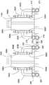
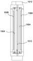
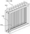
도 10a-10c는 일 실시예에 따른 듀얼 프로세싱 챔버들(110A, 110B)의 개략적인 도면들이다. 듀얼 프로세싱 챔버들(110A, 110B)은 각각의 프로세싱 챔버(110A, 110B)의 중심에서 선형 정렬로 배치된 복수의 마이크로파 안테나들(1010)을 포함한다. 안테나들(1010)은 프로세싱 챔버의 상단부로부터 프로세싱 챔버의 하단부까지 수직으로 연장된다. 각각의 마이크로파 안테나(1010)는 마이크로파 안테나(1010)에 결합된 프로세싱 챔버의 상단부 및 하단부 모두에서 대응 마이크로파 전력 헤드(1012)를 가진다. 도 10b에 도시된 바와 같이, 마이크로파 전력 헤드들(1012)은 엇갈려 배치된다(staggered). 엇갈린 배치는 공간적 제한들 때문일 수 있다. 전력은 각각의 전력 헤드(1012)를 통해서 안테나(1010)의 각 단부에 독립적으로 인가될 수 있다. 마이크로파 안테나들(1010)이 300 MHz 내지 300 GHz 범위 내의 주파수로 작동될 수 있다.10A-10C are schematic illustrations of
각각의 프로세싱 챔버들이, 마이크로파 안테나들(1010)의 각 측면 상에 하나씩, 2개의 기판들을 프로세싱할 수 있도록 정렬된다. 기판들은 플래튼(platen; 1008) 및 쉐도우 프레임(shadow frame; 1004)에 의해서 프로세싱 챔버 내의 제 위치에서 홀딩된다. 가스 도입 튜브들(1014)이 근처의 마이크로파 안테나들(1010) 사이에 배치된다. 가스 도입 튜브들(1014)은 마이크로파 안테나들(1010)에 평행하게 프로세싱 챔버의 하단부로부터 상단부까지 수직으로 연장된다. 가스 도입 튜브들(1014)은 실리콘 전구체들 및 질소 전구체들과 같은 프로세싱 가스들의 도입을 허용한다. 도 10a-도 10c에 도시되지는 않았지만, 프로세싱 챔버들(110A, 110B)은 기판 캐리어들(1008) 뒤쪽에 위치된 펌핑 포트를 통해서 진공배기될 수 있다.Each of the processing chambers is arranged to be capable of processing two substrates, one on each side of the
도 11a 및 도 11b는 다른 실시예에 따른 프로세싱 챔버(1100)의 개략적인 도면들이다. 프로세싱 챔버(1100)는 챔버 바디 내에서 제 1 단부(1108)로부터 제 2 단부(1118)까지 수직으로 연장되는, 마이크로파 안테나들과 같은, 복수의 플라즈마 발생기들을 포함한다. 프로세싱 챔버(1100)는 기판들의 프로세싱에서 이용하기 위한 플라즈마 발생기들(1102)의 각각의 측면 상에 쉐도우 프레임(1104)을 포함한다. 도 11b에 도시된 바와 같이, 쉐도우 프레임(1104)은 복수의 플라즈마 발생기들(1102)의 대향 측면들 상에 배치되며, 그에 따라 2개의 대면적 기판들이 하나의 프로세싱 챔버(1100) 내에서 프로세싱될 수 있고 그에 따라 동시에 또는 연속적으로 동일한 프로세싱 환경에 노출될 수 있다.11A and 11B are schematic illustrations of a
각각의 플라즈마 발생기(1102)가 그 플라즈마 발생기의 제 1 단부(1108)에서 제 1 도파관(1110)에 그리고 그 플라즈마 발생기의 제 2 단부(1118)에서 제 2 도파관(1116)에 결합된다. 각각의 제 1 도파관(1110)이 제 1 전력 소오스(1112)에 결합되는 한편, 각각의 제 2 도파관이 제 2 전력 소오스(1114)에 결합된다. 전력 소오스들(1112, 1114)이 외장(enclosure; 1106) 내에서 도파관들(1110, 1116)에 결합될 수 있다. 도 11b에 가장 잘 도시된 바와 같이, 외장들(1106)은 엇갈려 배치된 "T" 형상의 외장들이다. 공간적 제한들 때문에, 엇갈려 배치된 "T" 형상의 외장들이 필수적일 수 있다. 그러한 배열에서, 근처의 도파관들(1110, 1116)이 단부들(1108, 1118)로부터 각각의 전력 소오스들(1112, 1114)까지 반대의, 평행한 방향들을 따라 연장된다. 또한, 가스 도입 튜브들이 도 10c와 관련하여 전술한 방식으로 프로세싱 챔버(1100) 내에 배치될 수 있다.Each
도 12a 및 도 12b는 다른 실시예에 따른 프로세싱 챔버(1200)의 개략적인 도면들이다. 프로세싱 챔버(1200)는 제 1 단부(1208)로부터 제 2 단부(1218)까지 챔버 바디 내에서 수직으로 연장되는, 마이크로파 안테나들과 같은, 복수의 플라즈마 발생기들을 포함한다. 프로세싱 챔버(1200)는 기판들의 프로세싱에서 이용하기 위한 플라즈마 발생기들(1202)의 각각의 측면 상에 쉐도우 프레임(1204)을 포함한다. 도 12b에 도시된 바와 같이, 쉐도우 프레임(1204)은 복수의 플라즈마 발생기들(1202)의 대향 측면들 상에 배치되며, 그에 따라 2개의 대면적 기판들이 하나의 프로세싱 챔버(1200) 내에서 프로세싱될 수 있고 그에 따라 동시에 또는 연속적으로 동일한 프로세싱 환경에 노출될 수 있다.12A and 12B are schematic illustrations of a
각각의 플라즈마 발생기(1202)가 그 플라즈마 발생기의 제 1 단부(1208)에서 제 1 도파관(1210)에 그리고 그 플라즈마 발생기의 제 2 단부(1218)에서 제 2 도파관(1216)에 결합된다. 각각의 제 1 도파관(1210)이 제 1 전력 소오스(1212)에 결합되는 한편, 각각의 제 2 도파관이 제 2 전력 소오스(1214)에 결합된다. 전력 소오스들(1212, 1214)이 외장(1206) 내에서 도파관들(1210, 1216)에 결합될 수 있다. 도 12b에 가장 잘 도시된 바와 같이, 외장들(1206) 모두는 프로세싱 챔버(1200)의 동일한 측면으로부터 연장된다. 그러한 배열에서, 근처의 도파관들(1210, 1216)이 단부들(1208, 1218)로부터 각각의 전력 소오스들(1212, 1214)까지 동일한, 평행한 방향을 따라 연장된다. 또한, 가스 도입 튜브들이 도 10c와 관련하여 전술한 방식으로 프로세싱 챔버(1200) 내에 배치될 수 있다.Each
도 13a 및 도 13b는 다른 실시예에 따른 프로세싱 챔버(1300)의 개략적인 도면들이다. 프로세싱 챔버(1300)는 제 1 단부(1308)로부터 제 2 단부(1318)까지 챔버 바디 내에서 수직으로 연장되는, 마이크로파 안테나들과 같은, 복수의 플라즈마 발생기들을 포함한다. 프로세싱 챔버(1300)는 기판들의 프로세싱에서 이용하기 위한 플라즈마 발생기들(1302)의 각각의 측면 상에 쉐도우 프레임(1304)을 포함한다. 도 13b에 도시된 바와 같이, 쉐도우 프레임(1304)은 복수의 플라즈마 발생기들(1302)의 대향 측면들 상에 배치되며, 그에 따라 2개의 대면적 기판들이 하나의 프로세싱 챔버(1300) 내에서 프로세싱될 수 있고 그에 따라 동시에 또는 연속적으로 동일한 프로세싱 환경에 노출될 수 있다.13A and 13B are schematic illustrations of a
각각의 플라즈마 발생기(1302)가 그 플라즈마 발생기의 제 1 단부(1308)에서 제 1 각도형 도파관(1310)에 그리고 그 플라즈마 발생기의 제 2 단부(1318)에서 제 2 각도형 도파관(1316)에 결합된다. 각각의 제 1 각도형 도파관(1310)이 제 1 전력 소오스(1312)에 결합되는 한편, 각각의 제 2 각도형 도파관이 제 2 전력 소오스(1314)에 결합된다. 도파관들(1310, 1316)의 명료한 도시를 위해서 챔버의 측면으로부터 분리됨으로써, 외장들(1306)이 챔버(1300)의 상단부와 하단부 상에서 보여진다. 도 13b에 가장 잘 도시된 바와 같이, 도파관들(1310, 1316)이 프로세싱 챔버(1300)의 상단부를 따라서 그리고 프로세싱 챔버(1300)의 측면을 따라서 아래로 각각의 전력 소오스들(1312, 1314)까지 연장된다. 플라즈마 발생기들(1302)의 제 1 및 제 2 단부들(1308, 1318)에 대한 전력 소오스들(1312, 1314)의 위치로 인해서, 도파관들(1310, 1316)이 각도를 이룬다. 또한, 가스 도입 튜브들이 도 10c와 관련하여 전술한 방식으로 프로세싱 챔버(1300) 내에 배치될 수 있다.Each
수직 CVD 시스템을 이용함으로써, 복수의 기판들이 동시에 프로세싱될 수 있다. 복수의 기판들을 동시에 프로세싱하는 것은 제조 비용을 절감하며, 그러한 제조 비용 절감은 제조자의 이익들을 증가시킬 수 있다.By using the vertical CVD system, a plurality of substrates can be processed simultaneously. Processing a plurality of substrates simultaneously reduces manufacturing costs, and such manufacturing cost savings can increase the benefits of the manufacturer.
전술한 내용들이 본원 발명의 실시예들에 관한 것이지만, 본원 발명의 다른 실시예들 그리고 추가적인 실시예들이 본원 발명의 기본적인 범위로부터 벗어나지 않고도 고안될 수 있고, 본원 발명의 범위는 이하의 청구항들에 의해서 결정된다.While the foregoing is directed to embodiments of the present invention, other and further embodiments of the invention may be devised without departing from the basic scope thereof, and the scope of the invention is to be determined by the following claims .
Claims (20)
Translated fromKorean하나 또는 둘 이상의 제거가능 덮개들을 포함하는 챔버 바디로서, 각각의 덮개가 상기 챔버 바디의 각각의 측벽을 형성하고 하나 또는 둘 이상의 진공배기 라인들을 사용하여 챔버 바디를 진공시키기 위한 복수의 개구들을 포함하는, 챔버 바디;
복수의 플라즈마 발생기들의 대향 측면들 상에서 프로세싱되는 하나 또는 둘 이상의 기판들을 위한 충분한 공간이 상기 챔버 바디 내에 남도록, 상기 챔버 바디 내에서 수평으로 센터링(center)되고 그리고 상기 챔버 바디 내에서 수직으로 연장되는 복수의 플라즈마 발생기들 - 각각의 플라즈마 발생기는 상기 챔버 바디의 하단부 근처의 제 1 단부 및 상기 챔버 바디의 상단부 근처의 제 2 단부를 구비함 -;
각각의 플라즈마 발생기의 제 1 단부에 결합된 제 1 도파관;
각각의 플라즈마 발생기의 제 2 단부에 결합된 제 2 도파관;
상기 챔버 바디 외부에 배치되고, 각각의 제 1 도파관에 결합되는 제 1 전력 소오스;
상기 챔버 바디의 외부에 배치되고, 각각의 제 2 도파관에 결합되는 제 2 전력 소오스 - 상기 제 2 전력 소오스들은 근처의 제 2 도파관들이 상기 플라즈마 발생기들로부터 상응하는 제 2 전력 소오스들까지 공통 방향으로 연장되도록 패턴을 이루어 집합적으로 정렬됨 -; 및
상기 복수의 개구들에 결합되고 상기 하나 또는 둘 이상의 제거가능 덮개들을 제거할 경우 상기 하나 또는 둘 이상의 진공배기 라인들로부터 분리되도록 구성된 하나 또는 둘 이상의 수직 도관들;
을 포함하는,
장치.As a device:
CLAIMS What is claimed is: 1. A chamber body comprising one or more removable covers, each cover comprising a plurality of openings for forming respective side walls of the chamber body and for vacuuming the chamber body using one or more vacuum evacuation lines , Chamber body;
A plurality of plasma chambers that are horizontally centered within the chamber body and extend vertically within the chamber body such that sufficient space for one or more substrates to be processed on opposite sides of the plurality of plasma generators remains within the chamber body Each plasma generator having a first end near the lower end of the chamber body and a second end near the upper end of the chamber body;
A first waveguide coupled to a first end of each plasma generator;
A second waveguide coupled to a second end of each plasma generator;
A first power source disposed outside the chamber body and coupled to each first waveguide;
A second power source disposed outside the chamber body and coupled to each second waveguide, the second power sources having adjacent second waveguides in a common direction from the plasma generators to corresponding second power sources, Collectively arranged in a pattern to extend; And
One or more vertical conduits coupled to the plurality of openings and configured to separate from the one or more vacuum evacuation lines when the one or more removable covers are removed;
/ RTI >
Device.
하나 또는 둘 이상의 제거가능 덮개들을 포함하는 챔버 바디로서, 각각의 덮개가 상기 챔버 바디의 각각의 측벽을 형성하고 하나 또는 둘 이상의 진공배기 라인들을 사용하여 챔버 바디를 진공시키기 위한 복수의 개구들을 포함하는, 챔버 바디;
복수의 플라즈마 발생기들의 대향 측면들 상에서 프로세싱되는 하나 또는 둘 이상의 기판들을 위한 충분한 공간이 상기 챔버 바디 내에 남도록, 상기 챔버 바디 내에서 수평으로 센터링되고 그리고 상기 챔버 바디 내에서 수직으로 연장되는 복수의 플라즈마 발생기들 - 각각의 플라즈마 발생기는 상기 챔버 바디의 하단부 근처의 제 1 단부 및 상기 챔버 바디의 상단부 근처의 제 2 단부를 구비함 -;
상기 챔버 바디 내에 배치되고 상기 하나 또는 둘 이상의 기판들의 길이 방향 표면에 실질적으로 평행한 방향으로 연장되는 복수의 가스 도입 튜브들;
각각의 플라즈마 발생기의 제 1 단부에 결합된 제 1 도파관;
각각의 플라즈마 발생기의 제 2 단부에 결합된 제 2 도파관;
상기 챔버 바디 외부에 배치되고, 각각의 제 1 도파관에 결합되는 제 1 전력 소오스;
상기 챔버 바디의 외부에 배치되고, 각각의 제 2 도파관에 결합되는 제 2 전력 소오스 - 상기 제 2 전력 소오스들은 근처의 제 2 도파관들이 플라즈마 발생기들로부터 상응하는 제 2 전력 소오스들까지 동일한 방향으로 연장되도록 패턴을 이루어 집합적으로 정렬됨 -; 및
상기 복수의 개구들에 결합되고 상기 하나 또는 둘 이상의 제거가능 덮개들을 제거할 경우 상기 하나 또는 둘 이상의 진공배기 라인들로부터 분리되도록 구성된 하나 또는 둘 이상의 수직 도관들;
를 포함하는,
장치.As a device:
CLAIMS What is claimed is: 1. A chamber body comprising one or more removable covers, each cover comprising a plurality of openings for forming respective side walls of the chamber body and for vacuuming the chamber body using one or more vacuum evacuation lines , Chamber body;
A plurality of plasma generators that are horizontally centered within the chamber body and extend vertically in the chamber body such that sufficient space for one or more substrates to be processed on opposite sides of the plurality of plasma generators remains within the chamber body Each plasma generator having a first end near the lower end of the chamber body and a second end near the upper end of the chamber body;
A plurality of gas introduction tubes disposed in the chamber body and extending in a direction substantially parallel to a longitudinal surface of the one or more substrates;
A first waveguide coupled to a first end of each plasma generator;
A second waveguide coupled to a second end of each plasma generator;
A first power source disposed outside the chamber body and coupled to each first waveguide;
A second power source disposed outside the chamber body and coupled to each second waveguide, the second power sources having adjacent second waveguides extending in the same direction from the plasma generators to corresponding second power sources, Arranged in a pattern to form a pattern; And
One or more vertical conduits coupled to the plurality of openings and configured to separate from the one or more vacuum evacuation lines when the one or more removable covers are removed;
/ RTI >
Device.
하나 또는 둘 이상의 제거가능 덮개들을 포함하는 챔버 바디로서, 각각의 덮개가 상기 챔버 바디의 각각의 측벽을 형성하고 하나 또는 둘 이상의 진공배기 라인들을 사용하여 챔버 바디를 진공시키기 위한 복수의 개구들을 포함하는, 챔버 바디;
복수의 플라즈마 발생기들의 수평 대향 측면들의 각각의 측면 상에서 프로세싱되는 하나 또는 둘 이상의 기판들을 위한 충분한 공간이 상기 챔버 바디 내에 남도록, 상기 챔버 바디 내에서 수평으로 센터링되고 그리고 상기 챔버 바디 내에서 수직으로 연장되는 복수의 플라즈마 발생기들 - 각각의 플라즈마 발생기는 상기 챔버 바디의 하단부 근처의 제 1 단부 및 상기 챔버 바디의 상단부 근처의 제 2 단부를 구비함 -;
상기 챔버 바디 내에 배치되고 상기 수평 대향 측면들의 각각에 작용하도록 배치된 복수의 가스 도입 튜브들;
각각의 플라즈마 발생기의 제 1 단부에 결합된 제 1 각도형 도파관;
각각의 플라즈마 발생기의 제 2 단부에 결합된 제 2 각도형 도파관;
상기 챔버 바디 외부에 배치되고, 각각의 제 1 도파관에 결합되는 제 1 전력 소오스;
상기 챔버 바디의 외부에 배치되고, 각각의 제 2 도파관에 결합되는 제 2 전력 소오스 - 상기 제 2 전력 소오스들은 근처의 제 2 도파관들이 상기 플라즈마 발생기들로부터 상응하는 제 2 전력 소오스들까지 동일한 방향으로 연장되도록 패턴을 이루어 집합적으로 정렬됨 -; 및
상기 복수의 개구들에 결합되고 상기 하나 또는 둘 이상의 제거가능 덮개들을 제거할 경우 상기 하나 또는 둘 이상의 진공배기 라인들로부터 분리되도록 구성된 하나 또는 둘 이상의 수직 도관들;
를 포함하는,
장치.As a device:
CLAIMS What is claimed is: 1. A chamber body comprising one or more removable covers, each cover comprising a plurality of openings for forming respective side walls of the chamber body and for vacuuming the chamber body using one or more vacuum evacuation lines , Chamber body;
Centered within the chamber body and extending vertically within the chamber body such that sufficient space for one or more substrates to be processed on each side of the horizontally opposite sides of the plurality of plasma generators remains within the chamber body A plurality of plasma generators, each plasma generator having a first end near the lower end of the chamber body and a second end near the upper end of the chamber body;
A plurality of gas introduction tubes disposed in the chamber body and arranged to act on each of the horizontally opposed sides;
A first angled waveguide coupled to a first end of each plasma generator;
A second angled waveguide coupled to a second end of each plasma generator;
A first power source disposed outside the chamber body and coupled to each first waveguide;
A second power source disposed outside the chamber body and coupled to each second waveguide, the second power sources having adjacent second waveguides in the same direction from the plasma generators to corresponding second power sources, Collectively arranged in a pattern to extend; And
One or more vertical conduits coupled to the plurality of openings and configured to separate from the one or more vacuum evacuation lines when the one or more removable covers are removed;
/ RTI >
Device.
상기 복수의 플라즈마 발생기들이 마이크로파 발생기들인,
장치.The method according to claim 1,
Wherein the plurality of plasma generators are microwave generators,
Device.
복수의 상기 마이크로파 발생기들 근처에 그리고 상기 챔버 바디 내에 배치되는 복수의 가스 도입 튜브들을 더 포함하는,
장치.5. The method of claim 4,
Further comprising a plurality of gas introduction tubes disposed proximate to and within a plurality of said microwave generators,
Device.
상기 챔버 바디는 상기 복수의 마이크로파 발생기들에 접근하기 위해서 제거할 수 있는 하나 또는 둘 이상의 덮개들을 포함하고, 각각의 덮개는 관통하여 연장되는 복수의 개구부들을 구비하는,
장치.6. The method of claim 5,
Wherein the chamber body includes one or more covers removable to access the plurality of microwave generators, each cover having a plurality of openings extending therethrough,
Device.
각각의 덮개를 관통하여 연장되는 복수의 개구부들을 통해서 상기 챔버 바디가 진공배기(evacuate)될 수 있도록, 상기 챔버 바디와 결합된 하나 또는 둘 이상의 진공 펌프들을 더 포함하는,
장치.The method according to claim 6,
Further comprising one or more vacuum pumps coupled to the chamber body such that the chamber body can be evacuated through a plurality of openings extending through each of the lids.
Device.
상기 챔버 바디가 프레임 상에 배치되고, 그리고 상기 챔버 바디가 상기 프레임에 고정된 제 1 단부를 가지는,
장치.8. The method of claim 7,
Wherein the chamber body is disposed on a frame, and wherein the chamber body has a first end fixed to the frame,
Device.
상기 프레임 상에 배치된 폴리테트라플루오로에틸렌 부재를 더 포함하고, 상기 챔버 바디가 상기 폴리테트라플루오로에틸렌 부재 상에 배치된 제 2 단부를 구비하고 그리고 상기 폴리테트라플루오로에틸렌 부재를 따라서 이동될 수 있는,
장치.9. The method of claim 8,
Further comprising a polytetrafluoroethylene member disposed on the frame, wherein the chamber body has a second end disposed on the polytetrafluoroethylene member and is moved along the polytetrafluoroethylene member Can,
Device.
상기 챔버 바디는 상기 챔버 바디 내로 기판을 전달하기 위한 포트를 더 포함하고,
상기 포트는 상기 하나 또는 둘 이상의 제거가능 덮개들 중 하나를 포함하는 측벽 이외의 상기 챔버 바디의 측벽 상에 위치된
장치.The method according to claim 1,
Wherein the chamber body further comprises a port for delivering the substrate into the chamber body,
Wherein the port is located on a side wall of the chamber body other than a side wall comprising one of the one or more removable covers
Device.
상기 복수의 가스 도입 튜브들은 상기 챔버 바디 내에서 수직으로 연장되는,
장치.3. The method of claim 2,
Wherein the plurality of gas introduction tubes extend vertically in the chamber body,
Device.
상기 복수의 가스 도입 튜브들은 상기 복수의 플라즈마 발생기들 근처에 있는,
장치.3. The method of claim 2,
Wherein the plurality of gas introduction tubes are adjacent to the plurality of plasma generators,
Device.
각각의 가스 도입 튜브의 수평 위치가 상기 하나 또는 둘 이상의 기판들을 프로세싱하기 위한 챔버 바디 내에 남아 있는 공간과 상기 플라즈마 발생기들 사이에 있는
장치.3. The method of claim 2,
Wherein a horizontal position of each gas introduction tube is spaced apart from the space remaining in the chamber body for processing said one or more substrates and between said plasma generators
Device.
상기 복수의 가스 도입 튜브들이 상기 복수의 플라즈마 발생기들의 대향 측면들 상에 배치된,
장치.14. The method of claim 13,
Wherein the plurality of gas introduction tubes are disposed on opposite sides of the plurality of plasma generators,
Device.
상기 대향 측면들의 각각은 각각의 기판의 길이 방향 표면에 대응하고, 상기 대향 측면들 각각의 가스 도입 튜브들이 상기 각각의 기판의 길이 방향 표면의 방향을 따라 균일하게 이격된,
장치.15. The method of claim 14,
Each of the opposite sides corresponding to a longitudinal surface of a respective substrate and wherein gas introduction tubes of each of the opposite sides are uniformly spaced along the direction of the longitudinal surface of the respective substrate,
Device.
상기 복수의 가스 도입 튜브들은 상기 하나 또는 둘 이상의 기판들의 길이 방향 표면에 실질적으로 평행한 방향으로 연장되는,
장치.The method of claim 3,
Wherein the plurality of gas introduction tubes extend in a direction substantially parallel to a longitudinal surface of the one or more substrates,
Device.
상기 복수의 가스 도입 튜브들은 상기 챔버 바디 내에서 수직으로 연장되는,
장치.17. The method of claim 16,
Wherein the plurality of gas introduction tubes extend vertically in the chamber body,
Device.
상기 복수의 가스 도입 튜브들은 상기 복수의 플라즈마 발생기들 근처에 있는,
장치.The method of claim 3,
Wherein the plurality of gas introduction tubes are adjacent to the plurality of plasma generators,
Device.
각각의 가스 도입 튜브의 수평 위치가 상기 하나 또는 둘 이상의 기판들을 프로세싱하기 위한 챔버 바디 내에 남아 있는 공간과 상기 플라즈마 발생기들 사이에 있는
장치.The method of claim 3,
Wherein a horizontal position of each gas introduction tube is spaced apart from the space remaining in the chamber body for processing said one or more substrates and between said plasma generators
Device.
상기 수평 대향 측면들의 각각은 각각의 기판의 길이 방향 표면에 대응하고, 상기 수평 대향 측면들 각각의 가스 도입 튜브들이 상기 각각의 기판의 길이 방향 표면의 방향을 따라 균일하게 이격된,
장치.20. The method of claim 19,
Each of the horizontally opposed sides corresponding to a longitudinal surface of each substrate and wherein the gas introduction tubes of each of the horizontally opposed sides are uniformly spaced along the direction of the longitudinal surface of the respective substrate,
Device.
Applications Claiming Priority (7)
| Application Number | Priority Date | Filing Date | Title |
|---|---|---|---|
| US33029610P | 2010-04-30 | 2010-04-30 | |
| US61/330,296 | 2010-04-30 | ||
| US35423010P | 2010-06-13 | 2010-06-13 | |
| US61/354,230 | 2010-06-13 | ||
| US41653210P | 2010-11-23 | 2010-11-23 | |
| US61/416,532 | 2010-11-23 | ||
| PCT/US2011/034623WO2011137373A2 (en) | 2010-04-30 | 2011-04-29 | Vertical inline cvd system |
Publications (2)
| Publication Number | Publication Date |
|---|---|
| KR20130057441A KR20130057441A (en) | 2013-05-31 |
| KR101796656B1true KR101796656B1 (en) | 2017-11-13 |
Family
ID=44862144
Family Applications (2)
| Application Number | Title | Priority Date | Filing Date |
|---|---|---|---|
| KR1020127031556AExpired - Fee RelatedKR101796656B1 (en) | 2010-04-30 | 2011-04-29 | Vertical inline cvd system |
| KR1020127031554AExpired - Fee RelatedKR101932578B1 (en) | 2010-04-30 | 2011-04-29 | Vertical inline cvd system |
Family Applications After (1)
| Application Number | Title | Priority Date | Filing Date |
|---|---|---|---|
| KR1020127031554AExpired - Fee RelatedKR101932578B1 (en) | 2010-04-30 | 2011-04-29 | Vertical inline cvd system |
Country Status (6)
| Country | Link |
|---|---|
| US (2) | US9324597B2 (en) |
| JP (2) | JP5903429B2 (en) |
| KR (2) | KR101796656B1 (en) |
| CN (2) | CN102859034B (en) |
| TW (2) | TWI544107B (en) |
| WO (2) | WO2011137373A2 (en) |
Families Citing this family (385)
| Publication number | Priority date | Publication date | Assignee | Title |
|---|---|---|---|---|
| US10378106B2 (en) | 2008-11-14 | 2019-08-13 | Asm Ip Holding B.V. | Method of forming insulation film by modified PEALD |
| US9394608B2 (en) | 2009-04-06 | 2016-07-19 | Asm America, Inc. | Semiconductor processing reactor and components thereof |
| US8802201B2 (en) | 2009-08-14 | 2014-08-12 | Asm America, Inc. | Systems and methods for thin-film deposition of metal oxides using excited nitrogen-oxygen species |
| KR101796656B1 (en)* | 2010-04-30 | 2017-11-13 | 어플라이드 머티어리얼스, 인코포레이티드 | Vertical inline cvd system |
| US9312155B2 (en) | 2011-06-06 | 2016-04-12 | Asm Japan K.K. | High-throughput semiconductor-processing apparatus equipped with multiple dual-chamber modules |
| US9048518B2 (en) | 2011-06-21 | 2015-06-02 | Applied Materials, Inc. | Transmission line RF applicator for plasma chamber |
| US10364496B2 (en) | 2011-06-27 | 2019-07-30 | Asm Ip Holding B.V. | Dual section module having shared and unshared mass flow controllers |
| US10854498B2 (en) | 2011-07-15 | 2020-12-01 | Asm Ip Holding B.V. | Wafer-supporting device and method for producing same |
| US20130023129A1 (en) | 2011-07-20 | 2013-01-24 | Asm America, Inc. | Pressure transmitter for a semiconductor processing environment |
| US9644268B2 (en)* | 2011-08-31 | 2017-05-09 | Alta Devices, Inc. | Thermal bridge for chemical vapor deposition reactors |
| US9017481B1 (en) | 2011-10-28 | 2015-04-28 | Asm America, Inc. | Process feed management for semiconductor substrate processing |
| US9820372B2 (en) | 2012-01-27 | 2017-11-14 | Applied Materials, Inc. | Segmented antenna assembly |
| WO2013122954A1 (en)* | 2012-02-13 | 2013-08-22 | Applied Materials, Inc. | Linear pecvd apparatus |
| US9659799B2 (en) | 2012-08-28 | 2017-05-23 | Asm Ip Holding B.V. | Systems and methods for dynamic semiconductor process scheduling |
| US9021985B2 (en) | 2012-09-12 | 2015-05-05 | Asm Ip Holdings B.V. | Process gas management for an inductively-coupled plasma deposition reactor |
| US10714315B2 (en) | 2012-10-12 | 2020-07-14 | Asm Ip Holdings B.V. | Semiconductor reaction chamber showerhead |
| US20160376700A1 (en) | 2013-02-01 | 2016-12-29 | Asm Ip Holding B.V. | System for treatment of deposition reactor |
| US9484191B2 (en) | 2013-03-08 | 2016-11-01 | Asm Ip Holding B.V. | Pulsed remote plasma method and system |
| US9589770B2 (en) | 2013-03-08 | 2017-03-07 | Asm Ip Holding B.V. | Method and systems for in-situ formation of intermediate reactive species |
| US9240412B2 (en) | 2013-09-27 | 2016-01-19 | Asm Ip Holding B.V. | Semiconductor structure and device and methods of forming same using selective epitaxial process |
| TWI582028B (en)* | 2014-01-03 | 2017-05-11 | 緯創資通股份有限公司 | Feeder system and material guiding carrier thereof |
| US10683571B2 (en) | 2014-02-25 | 2020-06-16 | Asm Ip Holding B.V. | Gas supply manifold and method of supplying gases to chamber using same |
| US10167557B2 (en) | 2014-03-18 | 2019-01-01 | Asm Ip Holding B.V. | Gas distribution system, reactor including the system, and methods of using the same |
| US11015245B2 (en) | 2014-03-19 | 2021-05-25 | Asm Ip Holding B.V. | Gas-phase reactor and system having exhaust plenum and components thereof |
| JP2017516294A (en)* | 2014-05-09 | 2017-06-15 | アプライド マテリアルズ インコーポレイテッドApplied Materials,Incorporated | Substrate carrier system and method for using the same |
| WO2015171226A1 (en)* | 2014-05-09 | 2015-11-12 | Applied Materials, Inc. | Substrate carrier system with protective covering |
| US10858737B2 (en) | 2014-07-28 | 2020-12-08 | Asm Ip Holding B.V. | Showerhead assembly and components thereof |
| CN104195629A (en)* | 2014-08-20 | 2014-12-10 | 中国科学院半导体研究所 | Tower-type multichip epitaxial growth device |
| US9890456B2 (en) | 2014-08-21 | 2018-02-13 | Asm Ip Holding B.V. | Method and system for in situ formation of gas-phase compounds |
| US10941490B2 (en) | 2014-10-07 | 2021-03-09 | Asm Ip Holding B.V. | Multiple temperature range susceptor, assembly, reactor and system including the susceptor, and methods of using the same |
| US9657845B2 (en) | 2014-10-07 | 2017-05-23 | Asm Ip Holding B.V. | Variable conductance gas distribution apparatus and method |
| KR102263121B1 (en) | 2014-12-22 | 2021-06-09 | 에이에스엠 아이피 홀딩 비.브이. | Semiconductor device and manufacuring method thereof |
| US10529542B2 (en) | 2015-03-11 | 2020-01-07 | Asm Ip Holdings B.V. | Cross-flow reactor and method |
| US10276355B2 (en) | 2015-03-12 | 2019-04-30 | Asm Ip Holding B.V. | Multi-zone reactor, system including the reactor, and method of using the same |
| US10458018B2 (en) | 2015-06-26 | 2019-10-29 | Asm Ip Holding B.V. | Structures including metal carbide material, devices including the structures, and methods of forming same |
| US10600673B2 (en)* | 2015-07-07 | 2020-03-24 | Asm Ip Holding B.V. | Magnetic susceptor to baseplate seal |
| US10083836B2 (en) | 2015-07-24 | 2018-09-25 | Asm Ip Holding B.V. | Formation of boron-doped titanium metal films with high work function |
| KR102400863B1 (en)* | 2015-07-27 | 2022-05-24 | 삼성디스플레이 주식회사 | Apparatus of treating plasma and method of treating plasma subatrate using the same |
| US10039219B1 (en) | 2015-09-28 | 2018-07-31 | Western Digital Technologies, Inc. | Method and devices for picking and placing workpieces into devices under manufacture using dual robots |
| US9960072B2 (en) | 2015-09-29 | 2018-05-01 | Asm Ip Holding B.V. | Variable adjustment for precise matching of multiple chamber cavity housings |
| US10211308B2 (en) | 2015-10-21 | 2019-02-19 | Asm Ip Holding B.V. | NbMC layers |
| US10322384B2 (en) | 2015-11-09 | 2019-06-18 | Asm Ip Holding B.V. | Counter flow mixer for process chamber |
| US11139308B2 (en) | 2015-12-29 | 2021-10-05 | Asm Ip Holding B.V. | Atomic layer deposition of III-V compounds to form V-NAND devices |
| US10529554B2 (en) | 2016-02-19 | 2020-01-07 | Asm Ip Holding B.V. | Method for forming silicon nitride film selectively on sidewalls or flat surfaces of trenches |
| US10468251B2 (en) | 2016-02-19 | 2019-11-05 | Asm Ip Holding B.V. | Method for forming spacers using silicon nitride film for spacer-defined multiple patterning |
| US10501866B2 (en) | 2016-03-09 | 2019-12-10 | Asm Ip Holding B.V. | Gas distribution apparatus for improved film uniformity in an epitaxial system |
| US10343920B2 (en) | 2016-03-18 | 2019-07-09 | Asm Ip Holding B.V. | Aligned carbon nanotubes |
| US9892913B2 (en) | 2016-03-24 | 2018-02-13 | Asm Ip Holding B.V. | Radial and thickness control via biased multi-port injection settings |
| US10190213B2 (en) | 2016-04-21 | 2019-01-29 | Asm Ip Holding B.V. | Deposition of metal borides |
| US10865475B2 (en) | 2016-04-21 | 2020-12-15 | Asm Ip Holding B.V. | Deposition of metal borides and silicides |
| US10367080B2 (en) | 2016-05-02 | 2019-07-30 | Asm Ip Holding B.V. | Method of forming a germanium oxynitride film |
| US10032628B2 (en) | 2016-05-02 | 2018-07-24 | Asm Ip Holding B.V. | Source/drain performance through conformal solid state doping |
| KR102592471B1 (en) | 2016-05-17 | 2023-10-20 | 에이에스엠 아이피 홀딩 비.브이. | Method of forming metal interconnection and method of fabricating semiconductor device using the same |
| US11453943B2 (en) | 2016-05-25 | 2022-09-27 | Asm Ip Holding B.V. | Method for forming carbon-containing silicon/metal oxide or nitride film by ALD using silicon precursor and hydrocarbon precursor |
| US10388509B2 (en) | 2016-06-28 | 2019-08-20 | Asm Ip Holding B.V. | Formation of epitaxial layers via dislocation filtering |
| US10612137B2 (en) | 2016-07-08 | 2020-04-07 | Asm Ip Holdings B.V. | Organic reactants for atomic layer deposition |
| US9859151B1 (en) | 2016-07-08 | 2018-01-02 | Asm Ip Holding B.V. | Selective film deposition method to form air gaps |
| US10714385B2 (en) | 2016-07-19 | 2020-07-14 | Asm Ip Holding B.V. | Selective deposition of tungsten |
| KR102354490B1 (en) | 2016-07-27 | 2022-01-21 | 에이에스엠 아이피 홀딩 비.브이. | Method of processing a substrate |
| US10395919B2 (en) | 2016-07-28 | 2019-08-27 | Asm Ip Holding B.V. | Method and apparatus for filling a gap |
| KR102532607B1 (en) | 2016-07-28 | 2023-05-15 | 에이에스엠 아이피 홀딩 비.브이. | Substrate processing apparatus and method of operating the same |
| US9887082B1 (en) | 2016-07-28 | 2018-02-06 | Asm Ip Holding B.V. | Method and apparatus for filling a gap |
| US9812320B1 (en) | 2016-07-28 | 2017-11-07 | Asm Ip Holding B.V. | Method and apparatus for filling a gap |
| TWI588929B (en)* | 2016-08-01 | 2017-06-21 | 矽品精密工業股份有限公司 | Carrying device and its method of operation |
| US10410943B2 (en) | 2016-10-13 | 2019-09-10 | Asm Ip Holding B.V. | Method for passivating a surface of a semiconductor and related systems |
| US10643826B2 (en) | 2016-10-26 | 2020-05-05 | Asm Ip Holdings B.V. | Methods for thermally calibrating reaction chambers |
| US11532757B2 (en) | 2016-10-27 | 2022-12-20 | Asm Ip Holding B.V. | Deposition of charge trapping layers |
| US10435790B2 (en) | 2016-11-01 | 2019-10-08 | Asm Ip Holding B.V. | Method of subatmospheric plasma-enhanced ALD using capacitively coupled electrodes with narrow gap |
| US10229833B2 (en) | 2016-11-01 | 2019-03-12 | Asm Ip Holding B.V. | Methods for forming a transition metal nitride film on a substrate by atomic layer deposition and related semiconductor device structures |
| US10714350B2 (en) | 2016-11-01 | 2020-07-14 | ASM IP Holdings, B.V. | Methods for forming a transition metal niobium nitride film on a substrate by atomic layer deposition and related semiconductor device structures |
| US10643904B2 (en) | 2016-11-01 | 2020-05-05 | Asm Ip Holdings B.V. | Methods for forming a semiconductor device and related semiconductor device structures |
| US10134757B2 (en) | 2016-11-07 | 2018-11-20 | Asm Ip Holding B.V. | Method of processing a substrate and a device manufactured by using the method |
| KR102546317B1 (en) | 2016-11-15 | 2023-06-21 | 에이에스엠 아이피 홀딩 비.브이. | Gas supply unit and substrate processing apparatus including the same |
| US10340135B2 (en) | 2016-11-28 | 2019-07-02 | Asm Ip Holding B.V. | Method of topologically restricted plasma-enhanced cyclic deposition of silicon or metal nitride |
| KR102762543B1 (en) | 2016-12-14 | 2025-02-05 | 에이에스엠 아이피 홀딩 비.브이. | Substrate processing apparatus |
| US11581186B2 (en) | 2016-12-15 | 2023-02-14 | Asm Ip Holding B.V. | Sequential infiltration synthesis apparatus |
| US11447861B2 (en) | 2016-12-15 | 2022-09-20 | Asm Ip Holding B.V. | Sequential infiltration synthesis apparatus and a method of forming a patterned structure |
| KR102700194B1 (en) | 2016-12-19 | 2024-08-28 | 에이에스엠 아이피 홀딩 비.브이. | Substrate processing apparatus |
| US10269558B2 (en) | 2016-12-22 | 2019-04-23 | Asm Ip Holding B.V. | Method of forming a structure on a substrate |
| US10867788B2 (en) | 2016-12-28 | 2020-12-15 | Asm Ip Holding B.V. | Method of forming a structure on a substrate |
| US11390950B2 (en) | 2017-01-10 | 2022-07-19 | Asm Ip Holding B.V. | Reactor system and method to reduce residue buildup during a film deposition process |
| US10655221B2 (en) | 2017-02-09 | 2020-05-19 | Asm Ip Holding B.V. | Method for depositing oxide film by thermal ALD and PEALD |
| US10468261B2 (en) | 2017-02-15 | 2019-11-05 | Asm Ip Holding B.V. | Methods for forming a metallic film on a substrate by cyclical deposition and related semiconductor device structures |
| US10529563B2 (en) | 2017-03-29 | 2020-01-07 | Asm Ip Holdings B.V. | Method for forming doped metal oxide films on a substrate by cyclical deposition and related semiconductor device structures |
| US10283353B2 (en) | 2017-03-29 | 2019-05-07 | Asm Ip Holding B.V. | Method of reforming insulating film deposited on substrate with recess pattern |
| KR102457289B1 (en) | 2017-04-25 | 2022-10-21 | 에이에스엠 아이피 홀딩 비.브이. | Method for depositing a thin film and manufacturing a semiconductor device |
| US10892156B2 (en) | 2017-05-08 | 2021-01-12 | Asm Ip Holding B.V. | Methods for forming a silicon nitride film on a substrate and related semiconductor device structures |
| US10446393B2 (en) | 2017-05-08 | 2019-10-15 | Asm Ip Holding B.V. | Methods for forming silicon-containing epitaxial layers and related semiconductor device structures |
| US10770286B2 (en) | 2017-05-08 | 2020-09-08 | Asm Ip Holdings B.V. | Methods for selectively forming a silicon nitride film on a substrate and related semiconductor device structures |
| US10504742B2 (en) | 2017-05-31 | 2019-12-10 | Asm Ip Holding B.V. | Method of atomic layer etching using hydrogen plasma |
| US10886123B2 (en) | 2017-06-02 | 2021-01-05 | Asm Ip Holding B.V. | Methods for forming low temperature semiconductor layers and related semiconductor device structures |
| US12040200B2 (en) | 2017-06-20 | 2024-07-16 | Asm Ip Holding B.V. | Semiconductor processing apparatus and methods for calibrating a semiconductor processing apparatus |
| US11306395B2 (en) | 2017-06-28 | 2022-04-19 | Asm Ip Holding B.V. | Methods for depositing a transition metal nitride film on a substrate by atomic layer deposition and related deposition apparatus |
| US10685834B2 (en) | 2017-07-05 | 2020-06-16 | Asm Ip Holdings B.V. | Methods for forming a silicon germanium tin layer and related semiconductor device structures |
| KR20190009245A (en) | 2017-07-18 | 2019-01-28 | 에이에스엠 아이피 홀딩 비.브이. | Methods for forming a semiconductor device structure and related semiconductor device structures |
| US11374112B2 (en) | 2017-07-19 | 2022-06-28 | Asm Ip Holding B.V. | Method for depositing a group IV semiconductor and related semiconductor device structures |
| US10541333B2 (en) | 2017-07-19 | 2020-01-21 | Asm Ip Holding B.V. | Method for depositing a group IV semiconductor and related semiconductor device structures |
| US11018002B2 (en) | 2017-07-19 | 2021-05-25 | Asm Ip Holding B.V. | Method for selectively depositing a Group IV semiconductor and related semiconductor device structures |
| WO2019020167A1 (en)* | 2017-07-24 | 2019-01-31 | Applied Materials, Inc. | Apparatus and system for processing a substrate in a vacuum chamber, and method of transporting a carrier in a vacuum chamber |
| US10590535B2 (en) | 2017-07-26 | 2020-03-17 | Asm Ip Holdings B.V. | Chemical treatment, deposition and/or infiltration apparatus and method for using the same |
| US10312055B2 (en) | 2017-07-26 | 2019-06-04 | Asm Ip Holding B.V. | Method of depositing film by PEALD using negative bias |
| US10605530B2 (en) | 2017-07-26 | 2020-03-31 | Asm Ip Holding B.V. | Assembly of a liner and a flange for a vertical furnace as well as the liner and the vertical furnace |
| TWI815813B (en) | 2017-08-04 | 2023-09-21 | 荷蘭商Asm智慧財產控股公司 | Showerhead assembly for distributing a gas within a reaction chamber |
| US10770336B2 (en) | 2017-08-08 | 2020-09-08 | Asm Ip Holding B.V. | Substrate lift mechanism and reactor including same |
| US10692741B2 (en) | 2017-08-08 | 2020-06-23 | Asm Ip Holdings B.V. | Radiation shield |
| US11769682B2 (en) | 2017-08-09 | 2023-09-26 | Asm Ip Holding B.V. | Storage apparatus for storing cassettes for substrates and processing apparatus equipped therewith |
| US11139191B2 (en) | 2017-08-09 | 2021-10-05 | Asm Ip Holding B.V. | Storage apparatus for storing cassettes for substrates and processing apparatus equipped therewith |
| US10249524B2 (en) | 2017-08-09 | 2019-04-02 | Asm Ip Holding B.V. | Cassette holder assembly for a substrate cassette and holding member for use in such assembly |
| US10236177B1 (en) | 2017-08-22 | 2019-03-19 | ASM IP Holding B.V.. | Methods for depositing a doped germanium tin semiconductor and related semiconductor device structures |
| USD900036S1 (en) | 2017-08-24 | 2020-10-27 | Asm Ip Holding B.V. | Heater electrical connector and adapter |
| US11830730B2 (en) | 2017-08-29 | 2023-11-28 | Asm Ip Holding B.V. | Layer forming method and apparatus |
| US11056344B2 (en) | 2017-08-30 | 2021-07-06 | Asm Ip Holding B.V. | Layer forming method |
| US11295980B2 (en) | 2017-08-30 | 2022-04-05 | Asm Ip Holding B.V. | Methods for depositing a molybdenum metal film over a dielectric surface of a substrate by a cyclical deposition process and related semiconductor device structures |
| KR102491945B1 (en) | 2017-08-30 | 2023-01-26 | 에이에스엠 아이피 홀딩 비.브이. | Substrate processing apparatus |
| KR102401446B1 (en) | 2017-08-31 | 2022-05-24 | 에이에스엠 아이피 홀딩 비.브이. | Substrate processing apparatus |
| US10607895B2 (en) | 2017-09-18 | 2020-03-31 | Asm Ip Holdings B.V. | Method for forming a semiconductor device structure comprising a gate fill metal |
| KR102630301B1 (en) | 2017-09-21 | 2024-01-29 | 에이에스엠 아이피 홀딩 비.브이. | Method of sequential infiltration synthesis treatment of infiltrateable material and structures and devices formed using same |
| US10844484B2 (en) | 2017-09-22 | 2020-11-24 | Asm Ip Holding B.V. | Apparatus for dispensing a vapor phase reactant to a reaction chamber and related methods |
| US10658205B2 (en) | 2017-09-28 | 2020-05-19 | Asm Ip Holdings B.V. | Chemical dispensing apparatus and methods for dispensing a chemical to a reaction chamber |
| US10403504B2 (en) | 2017-10-05 | 2019-09-03 | Asm Ip Holding B.V. | Method for selectively depositing a metallic film on a substrate |
| US10319588B2 (en) | 2017-10-10 | 2019-06-11 | Asm Ip Holding B.V. | Method for depositing a metal chalcogenide on a substrate by cyclical deposition |
| US10861692B2 (en) | 2017-10-26 | 2020-12-08 | Taiwan Semiconductor Manufacturing Co., Ltd. | Substrate carrier deterioration detection and repair |
| US10923344B2 (en) | 2017-10-30 | 2021-02-16 | Asm Ip Holding B.V. | Methods for forming a semiconductor structure and related semiconductor structures |
| US10910262B2 (en) | 2017-11-16 | 2021-02-02 | Asm Ip Holding B.V. | Method of selectively depositing a capping layer structure on a semiconductor device structure |
| KR102443047B1 (en) | 2017-11-16 | 2022-09-14 | 에이에스엠 아이피 홀딩 비.브이. | Method of processing a substrate and a device manufactured by the same |
| US11022879B2 (en) | 2017-11-24 | 2021-06-01 | Asm Ip Holding B.V. | Method of forming an enhanced unexposed photoresist layer |
| WO2019103613A1 (en) | 2017-11-27 | 2019-05-31 | Asm Ip Holding B.V. | A storage device for storing wafer cassettes for use with a batch furnace |
| CN111344522B (en) | 2017-11-27 | 2022-04-12 | 阿斯莫Ip控股公司 | Including clean mini-environment device |
| US10290508B1 (en) | 2017-12-05 | 2019-05-14 | Asm Ip Holding B.V. | Method for forming vertical spacers for spacer-defined patterning |
| CN108048818A (en)* | 2017-12-18 | 2018-05-18 | 德淮半导体有限公司 | Chemical vapor deposition unit and its application method |
| US10872771B2 (en) | 2018-01-16 | 2020-12-22 | Asm Ip Holding B. V. | Method for depositing a material film on a substrate within a reaction chamber by a cyclical deposition process and related device structures |
| TWI799494B (en) | 2018-01-19 | 2023-04-21 | 荷蘭商Asm 智慧財產控股公司 | Deposition method |
| KR102695659B1 (en) | 2018-01-19 | 2024-08-14 | 에이에스엠 아이피 홀딩 비.브이. | Method for depositing a gap filling layer by plasma assisted deposition |
| USD903477S1 (en) | 2018-01-24 | 2020-12-01 | Asm Ip Holdings B.V. | Metal clamp |
| US11018047B2 (en) | 2018-01-25 | 2021-05-25 | Asm Ip Holding B.V. | Hybrid lift pin |
| US10535516B2 (en) | 2018-02-01 | 2020-01-14 | Asm Ip Holdings B.V. | Method for depositing a semiconductor structure on a surface of a substrate and related semiconductor structures |
| USD880437S1 (en) | 2018-02-01 | 2020-04-07 | Asm Ip Holding B.V. | Gas supply plate for semiconductor manufacturing apparatus |
| US11081345B2 (en) | 2018-02-06 | 2021-08-03 | Asm Ip Holding B.V. | Method of post-deposition treatment for silicon oxide film |
| WO2019158960A1 (en) | 2018-02-14 | 2019-08-22 | Asm Ip Holding B.V. | A method for depositing a ruthenium-containing film on a substrate by a cyclical deposition process |
| US10896820B2 (en) | 2018-02-14 | 2021-01-19 | Asm Ip Holding B.V. | Method for depositing a ruthenium-containing film on a substrate by a cyclical deposition process |
| US10731249B2 (en) | 2018-02-15 | 2020-08-04 | Asm Ip Holding B.V. | Method of forming a transition metal containing film on a substrate by a cyclical deposition process, a method for supplying a transition metal halide compound to a reaction chamber, and related vapor deposition apparatus |
| KR102636427B1 (en) | 2018-02-20 | 2024-02-13 | 에이에스엠 아이피 홀딩 비.브이. | Substrate processing method and apparatus |
| US10658181B2 (en) | 2018-02-20 | 2020-05-19 | Asm Ip Holding B.V. | Method of spacer-defined direct patterning in semiconductor fabrication |
| US10975470B2 (en) | 2018-02-23 | 2021-04-13 | Asm Ip Holding B.V. | Apparatus for detecting or monitoring for a chemical precursor in a high temperature environment |
| US11473195B2 (en) | 2018-03-01 | 2022-10-18 | Asm Ip Holding B.V. | Semiconductor processing apparatus and a method for processing a substrate |
| US12224156B2 (en) | 2018-03-01 | 2025-02-11 | Applied Materials, Inc. | Microwave plasma source for spatial plasma enhanced atomic layer deposition (PE-ALD) processing tool |
| TWI826925B (en) | 2018-03-01 | 2023-12-21 | 美商應用材料股份有限公司 | Plasma source assemblies and gas distribution assemblies |
| US11629406B2 (en) | 2018-03-09 | 2023-04-18 | Asm Ip Holding B.V. | Semiconductor processing apparatus comprising one or more pyrometers for measuring a temperature of a substrate during transfer of the substrate |
| US11114283B2 (en) | 2018-03-16 | 2021-09-07 | Asm Ip Holding B.V. | Reactor, system including the reactor, and methods of manufacturing and using same |
| KR102646467B1 (en) | 2018-03-27 | 2024-03-11 | 에이에스엠 아이피 홀딩 비.브이. | Method of forming an electrode on a substrate and a semiconductor device structure including an electrode |
| US10510536B2 (en) | 2018-03-29 | 2019-12-17 | Asm Ip Holding B.V. | Method of depositing a co-doped polysilicon film on a surface of a substrate within a reaction chamber |
| US11088002B2 (en) | 2018-03-29 | 2021-08-10 | Asm Ip Holding B.V. | Substrate rack and a substrate processing system and method |
| US11230766B2 (en) | 2018-03-29 | 2022-01-25 | Asm Ip Holding B.V. | Substrate processing apparatus and method |
| KR102501472B1 (en) | 2018-03-30 | 2023-02-20 | 에이에스엠 아이피 홀딩 비.브이. | Substrate processing method |
| KR102600229B1 (en) | 2018-04-09 | 2023-11-10 | 에이에스엠 아이피 홀딩 비.브이. | Substrate supporting device, substrate processing apparatus including the same and substrate processing method |
| US12025484B2 (en) | 2018-05-08 | 2024-07-02 | Asm Ip Holding B.V. | Thin film forming method |
| TWI811348B (en) | 2018-05-08 | 2023-08-11 | 荷蘭商Asm 智慧財產控股公司 | Methods for depositing an oxide film on a substrate by a cyclical deposition process and related device structures |
| US12272527B2 (en) | 2018-05-09 | 2025-04-08 | Asm Ip Holding B.V. | Apparatus for use with hydrogen radicals and method of using same |
| KR20190129718A (en) | 2018-05-11 | 2019-11-20 | 에이에스엠 아이피 홀딩 비.브이. | Methods for forming a doped metal carbide film on a substrate and related semiconductor device structures |
| KR102596988B1 (en) | 2018-05-28 | 2023-10-31 | 에이에스엠 아이피 홀딩 비.브이. | Method of processing a substrate and a device manufactured by the same |
| TWI840362B (en) | 2018-06-04 | 2024-05-01 | 荷蘭商Asm Ip私人控股有限公司 | Wafer handling chamber with moisture reduction |
| US11718913B2 (en) | 2018-06-04 | 2023-08-08 | Asm Ip Holding B.V. | Gas distribution system and reactor system including same |
| US11286562B2 (en) | 2018-06-08 | 2022-03-29 | Asm Ip Holding B.V. | Gas-phase chemical reactor and method of using same |
| KR102568797B1 (en) | 2018-06-21 | 2023-08-21 | 에이에스엠 아이피 홀딩 비.브이. | Substrate processing system |
| US10797133B2 (en) | 2018-06-21 | 2020-10-06 | Asm Ip Holding B.V. | Method for depositing a phosphorus doped silicon arsenide film and related semiconductor device structures |
| TWI873894B (en) | 2018-06-27 | 2025-02-21 | 荷蘭商Asm Ip私人控股有限公司 | Cyclic deposition methods for forming metal-containing material and films and structures including the metal-containing material |
| KR102854019B1 (en) | 2018-06-27 | 2025-09-02 | 에이에스엠 아이피 홀딩 비.브이. | Periodic deposition method for forming a metal-containing material and films and structures comprising the metal-containing material |
| KR102686758B1 (en) | 2018-06-29 | 2024-07-18 | 에이에스엠 아이피 홀딩 비.브이. | Method for depositing a thin film and manufacturing a semiconductor device |
| US10612136B2 (en) | 2018-06-29 | 2020-04-07 | ASM IP Holding, B.V. | Temperature-controlled flange and reactor system including same |
| US10755922B2 (en) | 2018-07-03 | 2020-08-25 | Asm Ip Holding B.V. | Method for depositing silicon-free carbon-containing film as gap-fill layer by pulse plasma-assisted deposition |
| US10388513B1 (en) | 2018-07-03 | 2019-08-20 | Asm Ip Holding B.V. | Method for depositing silicon-free carbon-containing film as gap-fill layer by pulse plasma-assisted deposition |
| US10767789B2 (en) | 2018-07-16 | 2020-09-08 | Asm Ip Holding B.V. | Diaphragm valves, valve components, and methods for forming valve components |
| US10483099B1 (en) | 2018-07-26 | 2019-11-19 | Asm Ip Holding B.V. | Method for forming thermally stable organosilicon polymer film |
| US11053591B2 (en) | 2018-08-06 | 2021-07-06 | Asm Ip Holding B.V. | Multi-port gas injection system and reactor system including same |
| US10883175B2 (en) | 2018-08-09 | 2021-01-05 | Asm Ip Holding B.V. | Vertical furnace for processing substrates and a liner for use therein |
| US10829852B2 (en) | 2018-08-16 | 2020-11-10 | Asm Ip Holding B.V. | Gas distribution device for a wafer processing apparatus |
| US11430674B2 (en) | 2018-08-22 | 2022-08-30 | Asm Ip Holding B.V. | Sensor array, apparatus for dispensing a vapor phase reactant to a reaction chamber and related methods |
| KR102707956B1 (en) | 2018-09-11 | 2024-09-19 | 에이에스엠 아이피 홀딩 비.브이. | Method for deposition of a thin film |
| US11024523B2 (en) | 2018-09-11 | 2021-06-01 | Asm Ip Holding B.V. | Substrate processing apparatus and method |
| US11049751B2 (en) | 2018-09-14 | 2021-06-29 | Asm Ip Holding B.V. | Cassette supply system to store and handle cassettes and processing apparatus equipped therewith |
| CN110970344B (en) | 2018-10-01 | 2024-10-25 | Asmip控股有限公司 | Substrate holding apparatus, system comprising the same and method of using the same |
| US11232963B2 (en) | 2018-10-03 | 2022-01-25 | Asm Ip Holding B.V. | Substrate processing apparatus and method |
| WO2020072507A1 (en) | 2018-10-04 | 2020-04-09 | Applied Materials, Inc. | Transport system |
| KR102592699B1 (en) | 2018-10-08 | 2023-10-23 | 에이에스엠 아이피 홀딩 비.브이. | Substrate support unit and apparatuses for depositing thin film and processing the substrate including the same |
| US10847365B2 (en) | 2018-10-11 | 2020-11-24 | Asm Ip Holding B.V. | Method of forming conformal silicon carbide film by cyclic CVD |
| US10811256B2 (en) | 2018-10-16 | 2020-10-20 | Asm Ip Holding B.V. | Method for etching a carbon-containing feature |
| KR102605121B1 (en) | 2018-10-19 | 2023-11-23 | 에이에스엠 아이피 홀딩 비.브이. | Substrate processing apparatus and substrate processing method |
| KR102546322B1 (en) | 2018-10-19 | 2023-06-21 | 에이에스엠 아이피 홀딩 비.브이. | Substrate processing apparatus and substrate processing method |
| USD948463S1 (en) | 2018-10-24 | 2022-04-12 | Asm Ip Holding B.V. | Susceptor for semiconductor substrate supporting apparatus |
| US10381219B1 (en) | 2018-10-25 | 2019-08-13 | Asm Ip Holding B.V. | Methods for forming a silicon nitride film |
| US12378665B2 (en) | 2018-10-26 | 2025-08-05 | Asm Ip Holding B.V. | High temperature coatings for a preclean and etch apparatus and related methods |
| US11145517B2 (en)* | 2018-10-29 | 2021-10-12 | Taiwan Semiconductor Manufacturing Co., Ltd. | Gas curtain for semiconductor manufacturing system |
| US11087997B2 (en) | 2018-10-31 | 2021-08-10 | Asm Ip Holding B.V. | Substrate processing apparatus for processing substrates |
| KR102748291B1 (en) | 2018-11-02 | 2024-12-31 | 에이에스엠 아이피 홀딩 비.브이. | Substrate support unit and substrate processing apparatus including the same |
| US11572620B2 (en) | 2018-11-06 | 2023-02-07 | Asm Ip Holding B.V. | Methods for selectively depositing an amorphous silicon film on a substrate |
| US11031242B2 (en) | 2018-11-07 | 2021-06-08 | Asm Ip Holding B.V. | Methods for depositing a boron doped silicon germanium film |
| US10847366B2 (en) | 2018-11-16 | 2020-11-24 | Asm Ip Holding B.V. | Methods for depositing a transition metal chalcogenide film on a substrate by a cyclical deposition process |
| US10818758B2 (en) | 2018-11-16 | 2020-10-27 | Asm Ip Holding B.V. | Methods for forming a metal silicate film on a substrate in a reaction chamber and related semiconductor device structures |
| US10559458B1 (en) | 2018-11-26 | 2020-02-11 | Asm Ip Holding B.V. | Method of forming oxynitride film |
| US12040199B2 (en) | 2018-11-28 | 2024-07-16 | Asm Ip Holding B.V. | Substrate processing apparatus for processing substrates |
| US11217444B2 (en) | 2018-11-30 | 2022-01-04 | Asm Ip Holding B.V. | Method for forming an ultraviolet radiation responsive metal oxide-containing film |
| KR102636428B1 (en) | 2018-12-04 | 2024-02-13 | 에이에스엠 아이피 홀딩 비.브이. | A method for cleaning a substrate processing apparatus |
| US11158513B2 (en) | 2018-12-13 | 2021-10-26 | Asm Ip Holding B.V. | Methods for forming a rhenium-containing film on a substrate by a cyclical deposition process and related semiconductor device structures |
| TWI874340B (en) | 2018-12-14 | 2025-03-01 | 荷蘭商Asm Ip私人控股有限公司 | Method of forming device structure, structure formed by the method and system for performing the method |
| US11694913B2 (en)* | 2018-12-18 | 2023-07-04 | Intevac, Inc. | Hybrid system architecture for thin film deposition |
| TWI866480B (en) | 2019-01-17 | 2024-12-11 | 荷蘭商Asm Ip 私人控股有限公司 | Methods of forming a transition metal containing film on a substrate by a cyclical deposition process |
| KR102727227B1 (en) | 2019-01-22 | 2024-11-07 | 에이에스엠 아이피 홀딩 비.브이. | Semiconductor processing device |
| CN111524788B (en) | 2019-02-01 | 2023-11-24 | Asm Ip私人控股有限公司 | Method for forming topologically selective films of silicon oxide |
| TWI838458B (en) | 2019-02-20 | 2024-04-11 | 荷蘭商Asm Ip私人控股有限公司 | Apparatus and methods for plug fill deposition in 3-d nand applications |
| KR102626263B1 (en) | 2019-02-20 | 2024-01-16 | 에이에스엠 아이피 홀딩 비.브이. | Cyclical deposition method including treatment step and apparatus for same |
| TWI873122B (en) | 2019-02-20 | 2025-02-21 | 荷蘭商Asm Ip私人控股有限公司 | Method of filling a recess formed within a surface of a substrate, semiconductor structure formed according to the method, and semiconductor processing apparatus |
| TWI845607B (en) | 2019-02-20 | 2024-06-21 | 荷蘭商Asm Ip私人控股有限公司 | Cyclical deposition method and apparatus for filling a recess formed within a substrate surface |
| TWI842826B (en) | 2019-02-22 | 2024-05-21 | 荷蘭商Asm Ip私人控股有限公司 | Substrate processing apparatus and method for processing substrate |
| CN111868298A (en)* | 2019-02-28 | 2020-10-30 | 东芝三菱电机产业系统株式会社 | Film forming device |
| US11742198B2 (en) | 2019-03-08 | 2023-08-29 | Asm Ip Holding B.V. | Structure including SiOCN layer and method of forming same |
| KR102782593B1 (en) | 2019-03-08 | 2025-03-14 | 에이에스엠 아이피 홀딩 비.브이. | Structure Including SiOC Layer and Method of Forming Same |
| KR102858005B1 (en) | 2019-03-08 | 2025-09-09 | 에이에스엠 아이피 홀딩 비.브이. | Method for Selective Deposition of Silicon Nitride Layer and Structure Including Selectively-Deposited Silicon Nitride Layer |
| JP2020167398A (en) | 2019-03-28 | 2020-10-08 | エーエスエム・アイピー・ホールディング・ベー・フェー | Door openers and substrate processing equipment provided with door openers |
| KR102809999B1 (en) | 2019-04-01 | 2025-05-19 | 에이에스엠 아이피 홀딩 비.브이. | Method of manufacturing semiconductor device |
| KR20200123380A (en) | 2019-04-19 | 2020-10-29 | 에이에스엠 아이피 홀딩 비.브이. | Layer forming method and apparatus |
| KR20200125453A (en) | 2019-04-24 | 2020-11-04 | 에이에스엠 아이피 홀딩 비.브이. | Gas-phase reactor system and method of using same |
| KR20200130121A (en) | 2019-05-07 | 2020-11-18 | 에이에스엠 아이피 홀딩 비.브이. | Chemical source vessel with dip tube |
| US11289326B2 (en) | 2019-05-07 | 2022-03-29 | Asm Ip Holding B.V. | Method for reforming amorphous carbon polymer film |
| KR20200130652A (en) | 2019-05-10 | 2020-11-19 | 에이에스엠 아이피 홀딩 비.브이. | Method of depositing material onto a surface and structure formed according to the method |
| JP7612342B2 (en) | 2019-05-16 | 2025-01-14 | エーエスエム・アイピー・ホールディング・ベー・フェー | Wafer boat handling apparatus, vertical batch furnace and method |
| JP7598201B2 (en) | 2019-05-16 | 2024-12-11 | エーエスエム・アイピー・ホールディング・ベー・フェー | Wafer boat handling apparatus, vertical batch furnace and method |
| USD947913S1 (en) | 2019-05-17 | 2022-04-05 | Asm Ip Holding B.V. | Susceptor shaft |
| USD975665S1 (en) | 2019-05-17 | 2023-01-17 | Asm Ip Holding B.V. | Susceptor shaft |
| US11189516B2 (en) | 2019-05-24 | 2021-11-30 | Applied Materials, Inc. | Method for mask and substrate alignment |
| US11538706B2 (en) | 2019-05-24 | 2022-12-27 | Applied Materials, Inc. | System and method for aligning a mask with a substrate |
| USD935572S1 (en) | 2019-05-24 | 2021-11-09 | Asm Ip Holding B.V. | Gas channel plate |
| USD922229S1 (en) | 2019-06-05 | 2021-06-15 | Asm Ip Holding B.V. | Device for controlling a temperature of a gas supply unit |
| KR20200141002A (en) | 2019-06-06 | 2020-12-17 | 에이에스엠 아이피 홀딩 비.브이. | Method of using a gas-phase reactor system including analyzing exhausted gas |
| KR20200141931A (en) | 2019-06-10 | 2020-12-21 | 에이에스엠 아이피 홀딩 비.브이. | Method for cleaning quartz epitaxial chambers |
| KR20200143254A (en) | 2019-06-11 | 2020-12-23 | 에이에스엠 아이피 홀딩 비.브이. | Method of forming an electronic structure using an reforming gas, system for performing the method, and structure formed using the method |
| USD944946S1 (en) | 2019-06-14 | 2022-03-01 | Asm Ip Holding B.V. | Shower plate |
| USD931978S1 (en) | 2019-06-27 | 2021-09-28 | Asm Ip Holding B.V. | Showerhead vacuum transport |
| KR20210005515A (en) | 2019-07-03 | 2021-01-14 | 에이에스엠 아이피 홀딩 비.브이. | Temperature control assembly for substrate processing apparatus and method of using same |
| JP7499079B2 (en) | 2019-07-09 | 2024-06-13 | エーエスエム・アイピー・ホールディング・ベー・フェー | Plasma device using coaxial waveguide and substrate processing method |
| CN112216646A (en) | 2019-07-10 | 2021-01-12 | Asm Ip私人控股有限公司 | Substrate supporting assembly and substrate processing device comprising same |
| KR20210010307A (en) | 2019-07-16 | 2021-01-27 | 에이에스엠 아이피 홀딩 비.브이. | Substrate processing apparatus |
| KR102860110B1 (en) | 2019-07-17 | 2025-09-16 | 에이에스엠 아이피 홀딩 비.브이. | Methods of forming silicon germanium structures |
| KR20210010816A (en) | 2019-07-17 | 2021-01-28 | 에이에스엠 아이피 홀딩 비.브이. | Radical assist ignition plasma system and method |
| US11643724B2 (en) | 2019-07-18 | 2023-05-09 | Asm Ip Holding B.V. | Method of forming structures using a neutral beam |
| CN110331378B (en)* | 2019-07-18 | 2024-01-19 | 中国科学院金属研究所 | HFCVD equipment for continuous preparation of diamond film and film plating method thereof |
| TWI839544B (en) | 2019-07-19 | 2024-04-21 | 荷蘭商Asm Ip私人控股有限公司 | Method of forming topology-controlled amorphous carbon polymer film |
| KR20210010817A (en) | 2019-07-19 | 2021-01-28 | 에이에스엠 아이피 홀딩 비.브이. | Method of Forming Topology-Controlled Amorphous Carbon Polymer Film |
| US11756816B2 (en) | 2019-07-26 | 2023-09-12 | Applied Materials, Inc. | Carrier FOUP and a method of placing a carrier |
| US11196360B2 (en) | 2019-07-26 | 2021-12-07 | Applied Materials, Inc. | System and method for electrostatically chucking a substrate to a carrier |
| US10916464B1 (en) | 2019-07-26 | 2021-02-09 | Applied Materials, Inc. | Method of pre aligning carrier, wafer and carrier-wafer combination for throughput efficiency |
| TWI851767B (en) | 2019-07-29 | 2024-08-11 | 荷蘭商Asm Ip私人控股有限公司 | Methods for selective deposition utilizing n-type dopants and/or alternative dopants to achieve high dopant incorporation |
| CN112309899A (en) | 2019-07-30 | 2021-02-02 | Asm Ip私人控股有限公司 | Substrate processing apparatus |
| US12169361B2 (en) | 2019-07-30 | 2024-12-17 | Asm Ip Holding B.V. | Substrate processing apparatus and method |
| CN112309900A (en) | 2019-07-30 | 2021-02-02 | Asm Ip私人控股有限公司 | Substrate processing apparatus |
| US11227782B2 (en) | 2019-07-31 | 2022-01-18 | Asm Ip Holding B.V. | Vertical batch furnace assembly |
| US11587814B2 (en) | 2019-07-31 | 2023-02-21 | Asm Ip Holding B.V. | Vertical batch furnace assembly |
| US11587815B2 (en) | 2019-07-31 | 2023-02-21 | Asm Ip Holding B.V. | Vertical batch furnace assembly |
| CN112323048B (en) | 2019-08-05 | 2024-02-09 | Asm Ip私人控股有限公司 | Liquid level sensor for chemical source container |
| CN112342526A (en) | 2019-08-09 | 2021-02-09 | Asm Ip私人控股有限公司 | Heater assembly including cooling device and method of using same |
| USD965524S1 (en) | 2019-08-19 | 2022-10-04 | Asm Ip Holding B.V. | Susceptor support |
| USD965044S1 (en) | 2019-08-19 | 2022-09-27 | Asm Ip Holding B.V. | Susceptor shaft |
| JP2021031769A (en) | 2019-08-21 | 2021-03-01 | エーエスエム アイピー ホールディング ビー.ブイ. | Production apparatus of mixed gas of film deposition raw material and film deposition apparatus |
| KR20210024423A (en) | 2019-08-22 | 2021-03-05 | 에이에스엠 아이피 홀딩 비.브이. | Method for forming a structure with a hole |
| USD930782S1 (en) | 2019-08-22 | 2021-09-14 | Asm Ip Holding B.V. | Gas distributor |
| USD979506S1 (en) | 2019-08-22 | 2023-02-28 | Asm Ip Holding B.V. | Insulator |
| USD949319S1 (en) | 2019-08-22 | 2022-04-19 | Asm Ip Holding B.V. | Exhaust duct |
| USD940837S1 (en) | 2019-08-22 | 2022-01-11 | Asm Ip Holding B.V. | Electrode |
| KR20210024420A (en) | 2019-08-23 | 2021-03-05 | 에이에스엠 아이피 홀딩 비.브이. | Method for depositing silicon oxide film having improved quality by peald using bis(diethylamino)silane |
| US11286558B2 (en) | 2019-08-23 | 2022-03-29 | Asm Ip Holding B.V. | Methods for depositing a molybdenum nitride film on a surface of a substrate by a cyclical deposition process and related semiconductor device structures including a molybdenum nitride film |
| KR102806450B1 (en) | 2019-09-04 | 2025-05-12 | 에이에스엠 아이피 홀딩 비.브이. | Methods for selective deposition using a sacrificial capping layer |
| KR102733104B1 (en) | 2019-09-05 | 2024-11-22 | 에이에스엠 아이피 홀딩 비.브이. | Substrate processing apparatus |
| US11562901B2 (en) | 2019-09-25 | 2023-01-24 | Asm Ip Holding B.V. | Substrate processing method |
| CN112593212B (en) | 2019-10-02 | 2023-12-22 | Asm Ip私人控股有限公司 | Method for forming topologically selective silicon oxide film by cyclic plasma enhanced deposition process |
| TW202128273A (en) | 2019-10-08 | 2021-08-01 | 荷蘭商Asm Ip私人控股有限公司 | Gas injection system, reactor system, and method of depositing material on surface of substratewithin reaction chamber |
| TWI846953B (en) | 2019-10-08 | 2024-07-01 | 荷蘭商Asm Ip私人控股有限公司 | Substrate processing device |
| KR20210042810A (en) | 2019-10-08 | 2021-04-20 | 에이에스엠 아이피 홀딩 비.브이. | Reactor system including a gas distribution assembly for use with activated species and method of using same |
| TWI846966B (en) | 2019-10-10 | 2024-07-01 | 荷蘭商Asm Ip私人控股有限公司 | Method of forming a photoresist underlayer and structure including same |
| US12009241B2 (en) | 2019-10-14 | 2024-06-11 | Asm Ip Holding B.V. | Vertical batch furnace assembly with detector to detect cassette |
| TWI834919B (en) | 2019-10-16 | 2024-03-11 | 荷蘭商Asm Ip私人控股有限公司 | Method of topology-selective film formation of silicon oxide |
| US11637014B2 (en) | 2019-10-17 | 2023-04-25 | Asm Ip Holding B.V. | Methods for selective deposition of doped semiconductor material |
| KR102845724B1 (en) | 2019-10-21 | 2025-08-13 | 에이에스엠 아이피 홀딩 비.브이. | Apparatus and methods for selectively etching films |
| KR20210050453A (en) | 2019-10-25 | 2021-05-07 | 에이에스엠 아이피 홀딩 비.브이. | Methods for filling a gap feature on a substrate surface and related semiconductor structures |
| US11646205B2 (en) | 2019-10-29 | 2023-05-09 | Asm Ip Holding B.V. | Methods of selectively forming n-type doped material on a surface, systems for selectively forming n-type doped material, and structures formed using same |
| KR20210054983A (en) | 2019-11-05 | 2021-05-14 | 에이에스엠 아이피 홀딩 비.브이. | Structures with doped semiconductor layers and methods and systems for forming same |
| US11501968B2 (en) | 2019-11-15 | 2022-11-15 | Asm Ip Holding B.V. | Method for providing a semiconductor device with silicon filled gaps |
| KR102861314B1 (en) | 2019-11-20 | 2025-09-17 | 에이에스엠 아이피 홀딩 비.브이. | Method of depositing carbon-containing material on a surface of a substrate, structure formed using the method, and system for forming the structure |
| CN112951697B (en) | 2019-11-26 | 2025-07-29 | Asmip私人控股有限公司 | Substrate processing apparatus |
| US11450529B2 (en) | 2019-11-26 | 2022-09-20 | Asm Ip Holding B.V. | Methods for selectively forming a target film on a substrate comprising a first dielectric surface and a second metallic surface |
| CN120432376A (en) | 2019-11-29 | 2025-08-05 | Asm Ip私人控股有限公司 | Substrate processing apparatus |
| CN112885692B (en) | 2019-11-29 | 2025-08-15 | Asmip私人控股有限公司 | Substrate processing apparatus |
| JP7527928B2 (en) | 2019-12-02 | 2024-08-05 | エーエスエム・アイピー・ホールディング・ベー・フェー | Substrate processing apparatus and substrate processing method |
| KR20210070898A (en) | 2019-12-04 | 2021-06-15 | 에이에스엠 아이피 홀딩 비.브이. | Substrate processing apparatus |
| KR20210078405A (en) | 2019-12-17 | 2021-06-28 | 에이에스엠 아이피 홀딩 비.브이. | Method of forming vanadium nitride layer and structure including the vanadium nitride layer |
| KR20210080214A (en) | 2019-12-19 | 2021-06-30 | 에이에스엠 아이피 홀딩 비.브이. | Methods for filling a gap feature on a substrate and related semiconductor structures |
| JP7636892B2 (en) | 2020-01-06 | 2025-02-27 | エーエスエム・アイピー・ホールディング・ベー・フェー | Channeled Lift Pins |
| JP7730637B2 (en) | 2020-01-06 | 2025-08-28 | エーエスエム・アイピー・ホールディング・ベー・フェー | Gas delivery assembly, components thereof, and reactor system including same |
| DE102020100171B3 (en)* | 2020-01-07 | 2021-07-01 | Cemecon Ag | Device for holding workpieces, coating system and method for coating a workpiece |
| US11993847B2 (en) | 2020-01-08 | 2024-05-28 | Asm Ip Holding B.V. | Injector |
| KR20210093163A (en) | 2020-01-16 | 2021-07-27 | 에이에스엠 아이피 홀딩 비.브이. | Method of forming high aspect ratio features |
| KR102675856B1 (en) | 2020-01-20 | 2024-06-17 | 에이에스엠 아이피 홀딩 비.브이. | Method of forming thin film and method of modifying surface of thin film |
| JP7522837B2 (en) | 2020-01-22 | 2024-07-25 | アプライド マテリアルズ インコーポレイテッド | In-line monitoring of OLED layer thickness and dopant concentration |
| EP4094307A4 (en) | 2020-01-22 | 2024-02-28 | Applied Materials, Inc. | INLINE MONITORING OF OLED LAYER THICKNESS AND DOPANT CONCENTRATION |
| TWI889744B (en) | 2020-01-29 | 2025-07-11 | 荷蘭商Asm Ip私人控股有限公司 | Contaminant trap system, and baffle plate stack |
| TW202513845A (en) | 2020-02-03 | 2025-04-01 | 荷蘭商Asm Ip私人控股有限公司 | Semiconductor structures and methods for forming the same |
| KR20210100010A (en) | 2020-02-04 | 2021-08-13 | 에이에스엠 아이피 홀딩 비.브이. | Method and apparatus for transmittance measurements of large articles |
| US11776846B2 (en) | 2020-02-07 | 2023-10-03 | Asm Ip Holding B.V. | Methods for depositing gap filling fluids and related systems and devices |
| KR20210103956A (en) | 2020-02-13 | 2021-08-24 | 에이에스엠 아이피 홀딩 비.브이. | Substrate processing apparatus including light receiving device and calibration method of light receiving device |
| TW202146691A (en) | 2020-02-13 | 2021-12-16 | 荷蘭商Asm Ip私人控股有限公司 | Gas distribution assembly, shower plate assembly, and method of adjusting conductance of gas to reaction chamber |
| TWI855223B (en) | 2020-02-17 | 2024-09-11 | 荷蘭商Asm Ip私人控股有限公司 | Method for growing phosphorous-doped silicon layer |
| CN113410160A (en) | 2020-02-28 | 2021-09-17 | Asm Ip私人控股有限公司 | System specially used for cleaning parts |
| KR20210113043A (en) | 2020-03-04 | 2021-09-15 | 에이에스엠 아이피 홀딩 비.브이. | Alignment fixture for a reactor system |
| US11876356B2 (en) | 2020-03-11 | 2024-01-16 | Asm Ip Holding B.V. | Lockout tagout assembly and system and method of using same |
| KR20210116240A (en) | 2020-03-11 | 2021-09-27 | 에이에스엠 아이피 홀딩 비.브이. | Substrate handling device with adjustable joints |
| KR102775390B1 (en) | 2020-03-12 | 2025-02-28 | 에이에스엠 아이피 홀딩 비.브이. | Method for Fabricating Layer Structure Having Target Topological Profile |
| US12173404B2 (en) | 2020-03-17 | 2024-12-24 | Asm Ip Holding B.V. | Method of depositing epitaxial material, structure formed using the method, and system for performing the method |
| KR102755229B1 (en) | 2020-04-02 | 2025-01-14 | 에이에스엠 아이피 홀딩 비.브이. | Thin film forming method |
| TWI887376B (en) | 2020-04-03 | 2025-06-21 | 荷蘭商Asm Ip私人控股有限公司 | Method for manufacturing semiconductor device |
| TWI888525B (en) | 2020-04-08 | 2025-07-01 | 荷蘭商Asm Ip私人控股有限公司 | Apparatus and methods for selectively etching silcon oxide films |
| US11821078B2 (en) | 2020-04-15 | 2023-11-21 | Asm Ip Holding B.V. | Method for forming precoat film and method for forming silicon-containing film |
| KR20210128343A (en) | 2020-04-15 | 2021-10-26 | 에이에스엠 아이피 홀딩 비.브이. | Method of forming chromium nitride layer and structure including the chromium nitride layer |
| US11996289B2 (en) | 2020-04-16 | 2024-05-28 | Asm Ip Holding B.V. | Methods of forming structures including silicon germanium and silicon layers, devices formed using the methods, and systems for performing the methods |
| KR20210130646A (en) | 2020-04-21 | 2021-11-01 | 에이에스엠 아이피 홀딩 비.브이. | Method for processing a substrate |
| KR102866804B1 (en) | 2020-04-24 | 2025-09-30 | 에이에스엠 아이피 홀딩 비.브이. | Vertical batch furnace assembly comprising a cooling gas supply |
| KR20210132612A (en) | 2020-04-24 | 2021-11-04 | 에이에스엠 아이피 홀딩 비.브이. | Methods and apparatus for stabilizing vanadium compounds |
| KR20210132600A (en) | 2020-04-24 | 2021-11-04 | 에이에스엠 아이피 홀딩 비.브이. | Methods and systems for depositing a layer comprising vanadium, nitrogen, and a further element |
| TW202208671A (en) | 2020-04-24 | 2022-03-01 | 荷蘭商Asm Ip私人控股有限公司 | Methods of forming structures including vanadium boride and vanadium phosphide layers |
| CN113555279A (en) | 2020-04-24 | 2021-10-26 | Asm Ip私人控股有限公司 | Methods of forming vanadium nitride-containing layers and structures comprising the same |
| KR102783898B1 (en) | 2020-04-29 | 2025-03-18 | 에이에스엠 아이피 홀딩 비.브이. | Solid source precursor vessel |
| KR20210134869A (en) | 2020-05-01 | 2021-11-11 | 에이에스엠 아이피 홀딩 비.브이. | Fast FOUP swapping with a FOUP handler |
| JP7726664B2 (en) | 2020-05-04 | 2025-08-20 | エーエスエム・アイピー・ホールディング・ベー・フェー | Substrate processing system for processing a substrate |
| KR102788543B1 (en) | 2020-05-13 | 2025-03-27 | 에이에스엠 아이피 홀딩 비.브이. | Laser alignment fixture for a reactor system |
| TW202146699A (en) | 2020-05-15 | 2021-12-16 | 荷蘭商Asm Ip私人控股有限公司 | Method of forming a silicon germanium layer, semiconductor structure, semiconductor device, method of forming a deposition layer, and deposition system |
| KR20210143653A (en) | 2020-05-19 | 2021-11-29 | 에이에스엠 아이피 홀딩 비.브이. | Substrate processing apparatus |
| KR20210145079A (en) | 2020-05-21 | 2021-12-01 | 에이에스엠 아이피 홀딩 비.브이. | Flange and apparatus for processing substrates |
| KR102795476B1 (en) | 2020-05-21 | 2025-04-11 | 에이에스엠 아이피 홀딩 비.브이. | Structures including multiple carbon layers and methods of forming and using same |
| TWI873343B (en) | 2020-05-22 | 2025-02-21 | 荷蘭商Asm Ip私人控股有限公司 | Reaction system for forming thin film on substrate |
| KR20210146802A (en) | 2020-05-26 | 2021-12-06 | 에이에스엠 아이피 홀딩 비.브이. | Method for depositing boron and gallium containing silicon germanium layers |
| TWI876048B (en) | 2020-05-29 | 2025-03-11 | 荷蘭商Asm Ip私人控股有限公司 | Substrate processing device |
| TW202212620A (en) | 2020-06-02 | 2022-04-01 | 荷蘭商Asm Ip私人控股有限公司 | Apparatus for processing substrate, method of forming film, and method of controlling apparatus for processing substrate |
| CN113774363A (en)* | 2020-06-09 | 2021-12-10 | 江苏菲沃泰纳米科技股份有限公司 | Film coating equipment and film coating method thereof |
| TW202208659A (en) | 2020-06-16 | 2022-03-01 | 荷蘭商Asm Ip私人控股有限公司 | Method for depositing boron containing silicon germanium layers |
| TW202218133A (en) | 2020-06-24 | 2022-05-01 | 荷蘭商Asm Ip私人控股有限公司 | Method for forming a layer provided with silicon |
| TWI873359B (en) | 2020-06-30 | 2025-02-21 | 荷蘭商Asm Ip私人控股有限公司 | Substrate processing method |
| US12431354B2 (en) | 2020-07-01 | 2025-09-30 | Asm Ip Holding B.V. | Silicon nitride and silicon oxide deposition methods using fluorine inhibitor |
| US11521870B2 (en)* | 2020-07-08 | 2022-12-06 | Applied Materials, Inc. | Annealing chamber |
| TW202202649A (en) | 2020-07-08 | 2022-01-16 | 荷蘭商Asm Ip私人控股有限公司 | Substrate processing method |
| KR20220010438A (en) | 2020-07-17 | 2022-01-25 | 에이에스엠 아이피 홀딩 비.브이. | Structures and methods for use in photolithography |
| TWI878570B (en) | 2020-07-20 | 2025-04-01 | 荷蘭商Asm Ip私人控股有限公司 | Method and system for depositing molybdenum layers |
| KR20220011092A (en) | 2020-07-20 | 2022-01-27 | 에이에스엠 아이피 홀딩 비.브이. | Method and system for forming structures including transition metal layers |
| US12322591B2 (en) | 2020-07-27 | 2025-06-03 | Asm Ip Holding B.V. | Thin film deposition process |
| KR20220021863A (en) | 2020-08-14 | 2022-02-22 | 에이에스엠 아이피 홀딩 비.브이. | Method for processing a substrate |
| US12040177B2 (en) | 2020-08-18 | 2024-07-16 | Asm Ip Holding B.V. | Methods for forming a laminate film by cyclical plasma-enhanced deposition processes |
| TW202228863A (en) | 2020-08-25 | 2022-08-01 | 荷蘭商Asm Ip私人控股有限公司 | Method for cleaning a substrate, method for selectively depositing, and reaction system |
| US11725280B2 (en) | 2020-08-26 | 2023-08-15 | Asm Ip Holding B.V. | Method for forming metal silicon oxide and metal silicon oxynitride layers |
| TW202229601A (en) | 2020-08-27 | 2022-08-01 | 荷蘭商Asm Ip私人控股有限公司 | Method of forming patterned structures, method of manipulating mechanical property, device structure, and substrate processing system |
| TW202217045A (en) | 2020-09-10 | 2022-05-01 | 荷蘭商Asm Ip私人控股有限公司 | Methods for depositing gap filing fluids and related systems and devices |
| USD990534S1 (en) | 2020-09-11 | 2023-06-27 | Asm Ip Holding B.V. | Weighted lift pin |
| KR20220036866A (en) | 2020-09-16 | 2022-03-23 | 에이에스엠 아이피 홀딩 비.브이. | Silicon oxide deposition method |
| USD1012873S1 (en) | 2020-09-24 | 2024-01-30 | Asm Ip Holding B.V. | Electrode for semiconductor processing apparatus |
| TWI889903B (en) | 2020-09-25 | 2025-07-11 | 荷蘭商Asm Ip私人控股有限公司 | Semiconductor processing method |
| US12009224B2 (en) | 2020-09-29 | 2024-06-11 | Asm Ip Holding B.V. | Apparatus and method for etching metal nitrides |
| KR20220045900A (en) | 2020-10-06 | 2022-04-13 | 에이에스엠 아이피 홀딩 비.브이. | Deposition method and an apparatus for depositing a silicon-containing material |
| CN114293174A (en) | 2020-10-07 | 2022-04-08 | Asm Ip私人控股有限公司 | Gas supply unit and substrate processing apparatus including the same |
| TW202229613A (en) | 2020-10-14 | 2022-08-01 | 荷蘭商Asm Ip私人控股有限公司 | Method of depositing material on stepped structure |
| TW202232565A (en) | 2020-10-15 | 2022-08-16 | 荷蘭商Asm Ip私人控股有限公司 | Method of manufacturing semiconductor device, and substrate treatment apparatus using ether-cat |
| TW202217037A (en) | 2020-10-22 | 2022-05-01 | 荷蘭商Asm Ip私人控股有限公司 | Method of depositing vanadium metal, structure, device and a deposition assembly |
| TW202223136A (en) | 2020-10-28 | 2022-06-16 | 荷蘭商Asm Ip私人控股有限公司 | Method for forming layer on substrate, and semiconductor processing system |
| TW202229620A (en) | 2020-11-12 | 2022-08-01 | 特文特大學 | Deposition system, method for controlling reaction condition, method for depositing |
| TW202229795A (en) | 2020-11-23 | 2022-08-01 | 荷蘭商Asm Ip私人控股有限公司 | A substrate processing apparatus with an injector |
| TW202235649A (en) | 2020-11-24 | 2022-09-16 | 荷蘭商Asm Ip私人控股有限公司 | Methods for filling a gap and related systems and devices |
| TW202235675A (en) | 2020-11-30 | 2022-09-16 | 荷蘭商Asm Ip私人控股有限公司 | Injector, and substrate processing apparatus |
| US12255053B2 (en) | 2020-12-10 | 2025-03-18 | Asm Ip Holding B.V. | Methods and systems for depositing a layer |
| TW202233884A (en) | 2020-12-14 | 2022-09-01 | 荷蘭商Asm Ip私人控股有限公司 | Method of forming structures for threshold voltage control |
| US11946137B2 (en) | 2020-12-16 | 2024-04-02 | Asm Ip Holding B.V. | Runout and wobble measurement fixtures |
| TW202232639A (en) | 2020-12-18 | 2022-08-16 | 荷蘭商Asm Ip私人控股有限公司 | Wafer processing apparatus with a rotatable table |
| TW202226899A (en) | 2020-12-22 | 2022-07-01 | 荷蘭商Asm Ip私人控股有限公司 | Plasma treatment device having matching box |
| TW202242184A (en) | 2020-12-22 | 2022-11-01 | 荷蘭商Asm Ip私人控股有限公司 | Precursor capsule, precursor vessel, vapor deposition assembly, and method of loading solid precursor into precursor vessel |
| TW202231903A (en) | 2020-12-22 | 2022-08-16 | 荷蘭商Asm Ip私人控股有限公司 | Transition metal deposition method, transition metal layer, and deposition assembly for depositing transition metal on substrate |
| USD980813S1 (en) | 2021-05-11 | 2023-03-14 | Asm Ip Holding B.V. | Gas flow control plate for substrate processing apparatus |
| USD980814S1 (en) | 2021-05-11 | 2023-03-14 | Asm Ip Holding B.V. | Gas distributor for substrate processing apparatus |
| USD1023959S1 (en) | 2021-05-11 | 2024-04-23 | Asm Ip Holding B.V. | Electrode for substrate processing apparatus |
| USD981973S1 (en) | 2021-05-11 | 2023-03-28 | Asm Ip Holding B.V. | Reactor wall for substrate processing apparatus |
| USD990441S1 (en) | 2021-09-07 | 2023-06-27 | Asm Ip Holding B.V. | Gas flow control plate |
| USD1060598S1 (en) | 2021-12-03 | 2025-02-04 | Asm Ip Holding B.V. | Split showerhead cover |
| TWI883497B (en)* | 2023-08-02 | 2025-05-11 | 友威科技股份有限公司 | Continuous processing mechanism for dual effect plasma etching |
Citations (2)
| Publication number | Priority date | Publication date | Assignee | Title |
|---|---|---|---|---|
| JP2005206852A (en)* | 2004-01-20 | 2005-08-04 | Ulvac Japan Ltd | Inline-type vacuum treatment apparatus |
| WO2009117229A2 (en)* | 2008-03-18 | 2009-09-24 | Applied Materials, Inc. | Coaxial microwave assisted deposition and etch systems |
Family Cites Families (97)
| Publication number | Priority date | Publication date | Assignee | Title |
|---|---|---|---|---|
| US4274936A (en)* | 1979-04-30 | 1981-06-23 | Advanced Coating Technology, Inc. | Vacuum deposition system and method |
| US4410558A (en)* | 1980-05-19 | 1983-10-18 | Energy Conversion Devices, Inc. | Continuous amorphous solar cell production system |
| US4423701A (en)* | 1982-03-29 | 1984-01-03 | Energy Conversion Devices, Inc. | Glow discharge deposition apparatus including a non-horizontally disposed cathode |
| US4474659A (en)* | 1982-05-28 | 1984-10-02 | Fazal Fazlin | Plated-through-hole method |
| US4576830A (en)* | 1984-11-05 | 1986-03-18 | Chronar Corp. | Deposition of materials |
| US4566403A (en)* | 1985-01-30 | 1986-01-28 | Sovonics Solar Systems | Apparatus for microwave glow discharge deposition |
| US4776918A (en) | 1986-10-20 | 1988-10-11 | Hitachi, Ltd. | Plasma processing apparatus |
| US4893584A (en)* | 1988-03-29 | 1990-01-16 | Energy Conversion Devices, Inc. | Large area microwave plasma apparatus |
| DE4029905C2 (en)* | 1990-09-21 | 1993-10-28 | Leybold Ag | Device for the transport of substrates |
| EP0577766B1 (en)* | 1991-04-04 | 1999-12-29 | Seagate Technology, Inc. | Apparatus and method for high throughput sputtering |
| US6124186A (en)* | 1992-05-05 | 2000-09-26 | Midwest Research Institute | Deposition of device quality, low hydrogen content, hydrogenated amorphous silicon at high deposition rates with increased stability using the hot wire filament technique |
| US5776819A (en)* | 1992-05-05 | 1998-07-07 | Midwest Research Institute | Deposition of device quality, low hydrogen content, amorphous silicon films by hot filament technique using "safe" silicon source gas |
| US5397737A (en)* | 1992-05-05 | 1995-03-14 | The United States Of America As Represented By The United States Department Of Energy | Deposition of device quality low H content, amorphous silicon films |
| JP3175333B2 (en)* | 1992-06-15 | 2001-06-11 | 日新電機株式会社 | Substrate processing equipment |
| DE69318480T2 (en)* | 1992-06-23 | 1998-09-17 | Nippon Telegraph & Telephone | Plasma processing device |
| US5252178A (en)* | 1992-06-24 | 1993-10-12 | Texas Instruments Incorporated | Multi-zone plasma processing method and apparatus |
| FR2701797B1 (en)* | 1993-02-18 | 1995-03-31 | Commissariat Energie Atomique | Microwave power transfer coupler to a plasma table and linear microwave source for plasma surface treatment. |
| US5614055A (en)* | 1993-08-27 | 1997-03-25 | Applied Materials, Inc. | High density plasma CVD and etching reactor |
| JPH07106094A (en) | 1993-10-04 | 1995-04-21 | Matsushita Electric Ind Co Ltd | Microwave plasma generator |
| JPH07161492A (en)* | 1993-12-06 | 1995-06-23 | Daido Steel Co Ltd | Microwave plasma processing equipment |
| DE4428136A1 (en)* | 1994-08-09 | 1996-02-15 | Leybold Ag | In-line vacuum coating plant, |
| JPH08138889A (en)* | 1994-09-16 | 1996-05-31 | Daihen Corp | Plasma treatment apparatus |
| EP0702393A3 (en)* | 1994-09-16 | 1997-03-26 | Daihen Corp | Plasma processing apparatus for radiating microwave from rectangular waveguide through long slot to plasma chamber |
| DE19503205C1 (en)* | 1995-02-02 | 1996-07-11 | Muegge Electronic Gmbh | Device for generating a plasma in low pressure container e.g. for hardware items surface treatment by plasma etching and plasma deposition |
| JP3360098B2 (en)* | 1995-04-20 | 2002-12-24 | 東京エレクトロン株式会社 | Shower head structure of processing equipment |
| JP3754742B2 (en)* | 1996-02-16 | 2006-03-15 | キヤノン株式会社 | Photovoltaic element manufacturing apparatus |
| DE19631407B4 (en)* | 1996-08-05 | 2006-05-04 | Unaxis Deutschland Holding Gmbh | Device for plasma-chemical deposition of polycrystalline diamond |
| DE19722272A1 (en)* | 1997-05-28 | 1998-12-03 | Leybold Systems Gmbh | Device for generating plasma |
| DE19739894C2 (en) | 1997-09-11 | 2001-07-05 | Muegge Electronic Gmbh | Plasma treatment device |
| JP3582330B2 (en)* | 1997-11-14 | 2004-10-27 | 東京エレクトロン株式会社 | Processing apparatus and processing system using the same |
| US6251183B1 (en)* | 1998-05-21 | 2001-06-26 | Midwest Research Institute | Rapid low-temperature epitaxial growth using a hot-element assisted chemical vapor deposition process |
| DE19824077A1 (en)* | 1998-05-29 | 1999-12-02 | Leybold Systems Gmbh | Device for generating plasma |
| US6214706B1 (en)* | 1998-08-28 | 2001-04-10 | Mv Systems, Inc. | Hot wire chemical vapor deposition method and apparatus using graphite hot rods |
| DE19841777C1 (en)* | 1998-09-12 | 2000-01-05 | Fraunhofer Ges Forschung | Apparatus for plasma-technological precipitation of polycrystalline diamond on substrates with large plane areas |
| EP0995812A1 (en)* | 1998-10-13 | 2000-04-26 | Vacumetal B.V. | Apparatus for flow-line treatment of articles in an artificial medium |
| WO2000043568A1 (en)* | 1999-01-22 | 2000-07-27 | Toyo Kohan Co., Ltd. | Microwave plasma cvd apparatus |
| US6186090B1 (en)* | 1999-03-04 | 2001-02-13 | Energy Conversion Devices, Inc. | Apparatus for the simultaneous deposition by physical vapor deposition and chemical vapor deposition and method therefor |
| JP4017796B2 (en) | 1999-10-26 | 2007-12-05 | 株式会社アルバック | Plasma processing equipment |
| JP4448586B2 (en)* | 2000-01-05 | 2010-04-14 | 株式会社アルバック | Large diameter carbon nanotube thin film forming plasma CVD apparatus and method for forming the thin film |
| US6635117B1 (en) | 2000-04-26 | 2003-10-21 | Axcelis Technologies, Inc. | Actively-cooled distribution plate for reducing reactive gas temperature in a plasma processing system |
| ES2336303T3 (en)* | 2000-05-17 | 2010-04-12 | Ihi Corporation | APPLIANCE AND PROCEDURE OF CVD BY PLASMA. |
| JP4856308B2 (en)* | 2000-12-27 | 2012-01-18 | キヤノンアネルバ株式会社 | Substrate processing apparatus and via chamber |
| US6793766B2 (en)* | 2001-01-04 | 2004-09-21 | Applied Materials Inc. | Apparatus having platforms positioned for precise centering of semiconductor wafers during processing |
| DE10114115A1 (en) | 2001-03-22 | 2002-10-02 | Muegge Electronic Gmbh | Structure for generating plasma in a treatment area fed with microwaves from outside feeds in microwaves through an opening in a protective screen effective for microwaves and partly surrounding the treatment area |
| US6638839B2 (en)* | 2001-07-26 | 2003-10-28 | The University Of Toledo | Hot-filament chemical vapor deposition chamber and process with multiple gas inlets |
| JP4564213B2 (en) | 2001-09-14 | 2010-10-20 | 三井造船株式会社 | Plasma generating antenna and CVD apparatus |
| JP4020679B2 (en) | 2002-04-09 | 2007-12-12 | シャープ株式会社 | Plasma process equipment |
| JP2004055614A (en)* | 2002-07-16 | 2004-02-19 | Tokyo Electron Ltd | Plasma processing apparatus |
| JP4120546B2 (en)* | 2002-10-04 | 2008-07-16 | 株式会社Ihi | Thin film forming method and apparatus, solar cell manufacturing method and apparatus, and solar cell |
| TWI262165B (en)* | 2002-10-16 | 2006-09-21 | Sez Ag | Device and method for transporting wafer-shaped articles |
| JP4087233B2 (en) | 2002-12-05 | 2008-05-21 | 株式会社アルバック | Plasma processing equipment |
| TW200415726A (en) | 2002-12-05 | 2004-08-16 | Adv Lcd Tech Dev Ct Co Ltd | Plasma processing apparatus and plasma processing method |
| US20040235299A1 (en) | 2003-05-22 | 2004-11-25 | Axcelis Technologies, Inc. | Plasma ashing apparatus and endpoint detection process |
| KR100441875B1 (en)* | 2003-06-02 | 2004-07-27 | 주성엔지니어링(주) | Separable type transfer chamber |
| DE102004008598B4 (en)* | 2004-02-21 | 2006-12-28 | Applied Films Gmbh & Co. Kg | Method for operating an in-line coating system |
| US20050183665A1 (en)* | 2004-02-24 | 2005-08-25 | Advanced Display Process Engineering Co., Ltd. | Apparatus for manufacturing flat-panel display |
| TWI274978B (en)* | 2004-02-25 | 2007-03-01 | Advanced Display Proc Eng Co | Apparatus for manufacturing flat-panel display |
| US7905960B2 (en)* | 2004-03-24 | 2011-03-15 | Jusung Engineering Co., Ltd. | Apparatus for manufacturing substrate |
| JP4471708B2 (en)* | 2004-03-31 | 2010-06-02 | キヤノンアネルバ株式会社 | Substrate transfer device |
| JP2005340425A (en)* | 2004-05-26 | 2005-12-08 | Ulvac Japan Ltd | Vacuum treatment device |
| US20070048456A1 (en)* | 2004-09-14 | 2007-03-01 | Keshner Marvin S | Plasma enhanced chemical vapor deposition apparatus and method |
| JP2006128000A (en) | 2004-10-29 | 2006-05-18 | Advanced Lcd Technologies Development Center Co Ltd | Plasma treatment device |
| US7267319B2 (en)* | 2004-11-09 | 2007-09-11 | General Electric Company | Low-friction slide-plates for rotary machines |
| JP4907077B2 (en)* | 2004-11-30 | 2012-03-28 | 株式会社Sen | Wafer processing apparatus, wafer processing method, and ion implantation apparatus |
| KR100667866B1 (en)* | 2004-12-22 | 2007-01-12 | 한국기계연구원 | Composite powder for lithium secondary battery negative electrode material, manufacturing method thereof and negative electrode material using same |
| US20060177288A1 (en)* | 2005-02-09 | 2006-08-10 | Parker N W | Multiple loadlocks and processing chamber |
| JP2006278643A (en) | 2005-03-29 | 2006-10-12 | Advanced Lcd Technologies Development Center Co Ltd | Plasma processing apparatus and plasm processing method |
| KR100667886B1 (en)* | 2005-07-01 | 2007-01-11 | 주식회사 에스에프에이 | Inline sputtering system |
| US7842355B2 (en)* | 2005-11-01 | 2010-11-30 | Applied Materials, Inc. | System and method for modulation of power and power related functions of PECVD discharge sources to achieve new film properties |
| US20070095281A1 (en)* | 2005-11-01 | 2007-05-03 | Stowell Michael W | System and method for power function ramping of microwave liner discharge sources |
| KR101225312B1 (en)* | 2005-12-16 | 2013-01-22 | 엘지디스플레이 주식회사 | Process apparatus |
| DE102006048814B4 (en)* | 2006-10-16 | 2014-01-16 | Iplas Innovative Plasma Systems Gmbh | Apparatus and method for generating high plasma density microwave plasmas |
| DE102006048815B4 (en)* | 2006-10-16 | 2016-03-17 | Iplas Innovative Plasma Systems Gmbh | Apparatus and method for generating high power microwave plasmas |
| US7976634B2 (en)* | 2006-11-21 | 2011-07-12 | Applied Materials, Inc. | Independent radiant gas preheating for precursor disassociation control and gas reaction kinetics in low temperature CVD systems |
| US20080127887A1 (en)* | 2006-12-01 | 2008-06-05 | Applied Materials, Inc. | Vertically mounted rotary cathodes in sputtering system on elevated rails |
| JP4896899B2 (en)* | 2007-01-31 | 2012-03-14 | 東京エレクトロン株式会社 | Substrate processing apparatus and particle adhesion preventing method |
| JP2010518604A (en)* | 2007-02-01 | 2010-05-27 | ウィラード アンド ケルシー ソーラー グループ, エルエルシー | Glass sheet semiconductor coating system and method and resulting product |
| US7972471B2 (en)* | 2007-06-29 | 2011-07-05 | Lam Research Corporation | Inductively coupled dual zone processing chamber with single planar antenna |
| WO2009009499A1 (en)* | 2007-07-07 | 2009-01-15 | Xunlight Corporation | Hybrid chemical vapor deposition process combining hot-wire cvd and plasma-enhanced cvd |
| CN101687229B (en) | 2007-07-12 | 2012-01-18 | 应用材料股份有限公司 | Apparatus and method for centering a substrate in a process chamber |
| US8197636B2 (en) | 2007-07-12 | 2012-06-12 | Applied Materials, Inc. | Systems for plasma enhanced chemical vapor deposition and bevel edge etching |
| JP5058084B2 (en) | 2007-07-27 | 2012-10-24 | 株式会社半導体エネルギー研究所 | Method for manufacturing photoelectric conversion device and microwave plasma CVD apparatus |
| JP2009094242A (en)* | 2007-10-05 | 2009-04-30 | Ebatekku:Kk | Substrate holding mechanism, substrate delivery mechanism, and substrate processing apparatus |
| JP2009105081A (en)* | 2007-10-19 | 2009-05-14 | Ebatekku:Kk | Substrate processing equipment |
| JP5307383B2 (en) | 2007-11-26 | 2013-10-02 | 株式会社アルバック | Vacuum processing equipment |
| KR101309363B1 (en)* | 2007-12-14 | 2013-09-17 | 가부시키가이샤 알박 | Chamber and film-forming apparatus |
| WO2011006109A2 (en)* | 2008-01-30 | 2011-01-13 | Applied Materials, Inc. | High efficiency low energy microwave ion/electron source |
| JP5302960B2 (en)* | 2008-06-06 | 2013-10-02 | 株式会社アルバック | Thin film solar cell manufacturing equipment |
| EP2299477B1 (en)* | 2008-06-06 | 2013-08-28 | Ulvac, Inc. | Thin- film solar cell manufacturing apparatus |
| CN102057076B (en)* | 2008-06-09 | 2013-03-06 | 应用材料公司 | Coating system and method for coating a substrate |
| US20090324368A1 (en)* | 2008-06-27 | 2009-12-31 | Applied Materials, Inc. | Processing system and method of operating a processing system |
| JP5511273B2 (en)* | 2008-09-12 | 2014-06-04 | 株式会社日立国際電気 | Substrate processing apparatus and substrate processing method |
| TW201130007A (en)* | 2009-07-09 | 2011-09-01 | Applied Materials Inc | High efficiency low energy microwave ion/electron source |
| WO2011059749A2 (en)* | 2009-10-28 | 2011-05-19 | Applied Materials, Inc. | Vertically integrated processing chamber |
| JP2011119396A (en)* | 2009-12-02 | 2011-06-16 | Ulvac Japan Ltd | Device for manufacturing thin film solar cell |
| KR101796656B1 (en)* | 2010-04-30 | 2017-11-13 | 어플라이드 머티어리얼스, 인코포레이티드 | Vertical inline cvd system |
| US20130068161A1 (en)* | 2011-09-15 | 2013-03-21 | Applied Materials, Inc. | Gas delivery and distribution for uniform process in linear-type large-area plasma reactor |
- 2011
- 2011-04-29KRKR1020127031556Apatent/KR101796656B1/ennot_activeExpired - Fee Related
- 2011-04-29USUS13/098,255patent/US9324597B2/ennot_activeExpired - Fee Related
- 2011-04-29KRKR1020127031554Apatent/KR101932578B1/ennot_activeExpired - Fee Related
- 2011-04-29CNCN201180020889.4Apatent/CN102859034B/ennot_activeExpired - Fee Related
- 2011-04-29WOPCT/US2011/034623patent/WO2011137373A2/enactiveApplication Filing
- 2011-04-29JPJP2013508289Apatent/JP5903429B2/ennot_activeExpired - Fee Related
- 2011-04-29JPJP2013508288Apatent/JP2013527609A/enactivePending
- 2011-04-29TWTW100115151Apatent/TWI544107B/ennot_activeIP Right Cessation
- 2011-04-29USUS13/098,253patent/US9922854B2/ennot_activeExpired - Fee Related
- 2011-04-29CNCN2011800216142Apatent/CN102859655A/enactivePending
- 2011-04-29WOPCT/US2011/034619patent/WO2011137371A2/enactiveApplication Filing
- 2011-04-29TWTW100115152Apatent/TWI551718B/ennot_activeIP Right Cessation
Patent Citations (2)
| Publication number | Priority date | Publication date | Assignee | Title |
|---|---|---|---|---|
| JP2005206852A (en)* | 2004-01-20 | 2005-08-04 | Ulvac Japan Ltd | Inline-type vacuum treatment apparatus |
| WO2009117229A2 (en)* | 2008-03-18 | 2009-09-24 | Applied Materials, Inc. | Coaxial microwave assisted deposition and etch systems |
Also Published As
| Publication number | Publication date |
|---|---|
| JP2013527609A (en) | 2013-06-27 |
| TW201204865A (en) | 2012-02-01 |
| KR101932578B1 (en) | 2018-12-28 |
| CN102859034A (en) | 2013-01-02 |
| US20120031335A1 (en) | 2012-02-09 |
| WO2011137373A2 (en) | 2011-11-03 |
| KR20130057441A (en) | 2013-05-31 |
| JP2013526067A (en) | 2013-06-20 |
| KR20130062942A (en) | 2013-06-13 |
| CN102859034B (en) | 2015-04-29 |
| TWI544107B (en) | 2016-08-01 |
| US9324597B2 (en) | 2016-04-26 |
| WO2011137373A4 (en) | 2012-03-15 |
| WO2011137373A3 (en) | 2012-02-09 |
| CN102859655A (en) | 2013-01-02 |
| US20120031333A1 (en) | 2012-02-09 |
| JP5903429B2 (en) | 2016-04-13 |
| TWI551718B (en) | 2016-10-01 |
| TW201202472A (en) | 2012-01-16 |
| WO2011137371A2 (en) | 2011-11-03 |
| US9922854B2 (en) | 2018-03-20 |
| WO2011137371A3 (en) | 2012-03-01 |
Similar Documents
| Publication | Publication Date | Title |
|---|---|---|
| KR101796656B1 (en) | Vertical inline cvd system | |
| KR102073485B1 (en) | Processing apparatus and processing method | |
| EP1159465B1 (en) | Method of atomic layer deposition | |
| US6902624B2 (en) | Massively parallel atomic layer deposition/chemical vapor deposition system | |
| US20080202892A1 (en) | Stacked process chambers for substrate vacuum processing tool | |
| US20140126980A1 (en) | Substrate processing apparatus | |
| US20080206036A1 (en) | Magnetic media processing tool with storage bays and multi-axis robot arms | |
| KR101100284B1 (en) | Thin film deposition apparatus | |
| US10483141B2 (en) | Semiconductor process equipment | |
| CN103361633B (en) | Gas inlet device, reaction cavity and plasma processing equipment | |
| US20080202419A1 (en) | Gas manifold directly attached to substrate processing chamber | |
| KR20190002415A (en) | Apparatus for processing a substrate, a processing system for processing a substrate, and a method for servicing an apparatus for processing a substrate | |
| US20080202687A1 (en) | Stacked process chambers for flat-panel display processing tool | |
| CN117248192A (en) | Substrate processing equipment including improved exhaust structure | |
| US20080206023A1 (en) | Semiconductor substrate processing apparatus with horizontally clustered vertical stacks | |
| US20080202686A1 (en) | Self-contained process modules for magnetic media processing tool | |
| US20080206020A1 (en) | Flat-panel display processing tool with storage bays and multi-axis robot arms | |
| KR102817950B1 (en) | fabrication line | |
| WO2013107766A1 (en) | Vacuum deposition system | |
| KR20230151914A (en) | Substrate Processing Apparatus including Exhaust Duct | |
| US20080202410A1 (en) | Multi-substrate size vacuum processing tool | |
| US20080202417A1 (en) | Self-contained process modules for vacuum processing tool | |
| TW201829817A (en) | Vacuum deposition apparatus and corresponding deposition module and method of depositing a layer on a substrate |
Legal Events
| Date | Code | Title | Description |
|---|---|---|---|
| PA0105 | International application | St.27 status event code:A-0-1-A10-A15-nap-PA0105 | |
| P11-X000 | Amendment of application requested | St.27 status event code:A-2-2-P10-P11-nap-X000 | |
| P13-X000 | Application amended | St.27 status event code:A-2-2-P10-P13-nap-X000 | |
| P11-X000 | Amendment of application requested | St.27 status event code:A-2-2-P10-P11-nap-X000 | |
| P13-X000 | Application amended | St.27 status event code:A-2-2-P10-P13-nap-X000 | |
| PG1501 | Laying open of application | St.27 status event code:A-1-1-Q10-Q12-nap-PG1501 | |
| PA0201 | Request for examination | St.27 status event code:A-1-2-D10-D11-exm-PA0201 | |
| E902 | Notification of reason for refusal | ||
| PE0902 | Notice of grounds for rejection | St.27 status event code:A-1-2-D10-D21-exm-PE0902 | |
| P11-X000 | Amendment of application requested | St.27 status event code:A-2-2-P10-P11-nap-X000 | |
| P13-X000 | Application amended | St.27 status event code:A-2-2-P10-P13-nap-X000 | |
| E701 | Decision to grant or registration of patent right | ||
| PE0701 | Decision of registration | St.27 status event code:A-1-2-D10-D22-exm-PE0701 | |
| GRNT | Written decision to grant | ||
| PR0701 | Registration of establishment | St.27 status event code:A-2-4-F10-F11-exm-PR0701 | |
| PR1002 | Payment of registration fee | St.27 status event code:A-2-2-U10-U12-oth-PR1002 Fee payment year number:1 | |
| PG1601 | Publication of registration | St.27 status event code:A-4-4-Q10-Q13-nap-PG1601 | |
| PC1903 | Unpaid annual fee | St.27 status event code:A-4-4-U10-U13-oth-PC1903 Not in force date:20201107 Payment event data comment text:Termination Category : DEFAULT_OF_REGISTRATION_FEE | |
| PC1903 | Unpaid annual fee | St.27 status event code:N-4-6-H10-H13-oth-PC1903 Ip right cessation event data comment text:Termination Category : DEFAULT_OF_REGISTRATION_FEE Not in force date:20201107 | |
| P22-X000 | Classification modified | St.27 status event code:A-4-4-P10-P22-nap-X000 |