KR101791713B1 - Field effect transistor and semiconductor device - Google Patents
Field effect transistor and semiconductor deviceDownload PDFInfo
- Publication number
- KR101791713B1 KR101791713B1KR1020127019627AKR20127019627AKR101791713B1KR 101791713 B1KR101791713 B1KR 101791713B1KR 1020127019627 AKR1020127019627 AKR 1020127019627AKR 20127019627 AKR20127019627 AKR 20127019627AKR 101791713 B1KR101791713 B1KR 101791713B1
- Authority
- KR
- South Korea
- Prior art keywords
- conductor electrode
- semiconductor layer
- gate
- electrode
- semiconductor
- Prior art date
- Legal status (The legal status is an assumption and is not a legal conclusion. Google has not performed a legal analysis and makes no representation as to the accuracy of the status listed.)
- Expired - Fee Related
Links
Images


Classifications
- H—ELECTRICITY
- H10—SEMICONDUCTOR DEVICES; ELECTRIC SOLID-STATE DEVICES NOT OTHERWISE PROVIDED FOR
- H10D—INORGANIC ELECTRIC SEMICONDUCTOR DEVICES
- H10D84/00—Integrated devices formed in or on semiconductor substrates that comprise only semiconducting layers, e.g. on Si wafers or on GaAs-on-Si wafers
- H10D84/80—Integrated devices formed in or on semiconductor substrates that comprise only semiconducting layers, e.g. on Si wafers or on GaAs-on-Si wafers characterised by the integration of at least one component covered by groups H10D12/00 or H10D30/00, e.g. integration of IGFETs
- H10D84/811—Combinations of field-effect devices and one or more diodes, capacitors or resistors
- H—ELECTRICITY
- H10—SEMICONDUCTOR DEVICES; ELECTRIC SOLID-STATE DEVICES NOT OTHERWISE PROVIDED FOR
- H10D—INORGANIC ELECTRIC SEMICONDUCTOR DEVICES
- H10D30/00—Field-effect transistors [FET]
- H10D30/60—Insulated-gate field-effect transistors [IGFET]
- H10D30/67—Thin-film transistors [TFT]
- H10D30/6704—Thin-film transistors [TFT] having supplementary regions or layers in the thin films or in the insulated bulk substrates for controlling properties of the device
- H10D30/6713—Thin-film transistors [TFT] having supplementary regions or layers in the thin films or in the insulated bulk substrates for controlling properties of the device characterised by the properties of the source or drain regions, e.g. compositions or sectional shapes
- H10D30/6715—Thin-film transistors [TFT] having supplementary regions or layers in the thin films or in the insulated bulk substrates for controlling properties of the device characterised by the properties of the source or drain regions, e.g. compositions or sectional shapes characterised by the doping profiles, e.g. having lightly-doped source or drain extensions
- H—ELECTRICITY
- H10—SEMICONDUCTOR DEVICES; ELECTRIC SOLID-STATE DEVICES NOT OTHERWISE PROVIDED FOR
- H10D—INORGANIC ELECTRIC SEMICONDUCTOR DEVICES
- H10D30/00—Field-effect transistors [FET]
- H10D30/60—Insulated-gate field-effect transistors [IGFET]
- H10D30/67—Thin-film transistors [TFT]
- H10D30/6729—Thin-film transistors [TFT] characterised by the electrodes
- H10D30/6737—Thin-film transistors [TFT] characterised by the electrodes characterised by the electrode materials
- H10D30/6739—Conductor-insulator-semiconductor electrodes
- H—ELECTRICITY
- H10—SEMICONDUCTOR DEVICES; ELECTRIC SOLID-STATE DEVICES NOT OTHERWISE PROVIDED FOR
- H10D—INORGANIC ELECTRIC SEMICONDUCTOR DEVICES
- H10D30/00—Field-effect transistors [FET]
- H10D30/60—Insulated-gate field-effect transistors [IGFET]
- H10D30/67—Thin-film transistors [TFT]
- H10D30/674—Thin-film transistors [TFT] characterised by the active materials
- H10D30/6741—Group IV materials, e.g. germanium or silicon carbide
- H—ELECTRICITY
- H10—SEMICONDUCTOR DEVICES; ELECTRIC SOLID-STATE DEVICES NOT OTHERWISE PROVIDED FOR
- H10D—INORGANIC ELECTRIC SEMICONDUCTOR DEVICES
- H10D30/00—Field-effect transistors [FET]
- H10D30/60—Insulated-gate field-effect transistors [IGFET]
- H10D30/67—Thin-film transistors [TFT]
- H10D30/674—Thin-film transistors [TFT] characterised by the active materials
- H10D30/6755—Oxide semiconductors, e.g. zinc oxide, copper aluminium oxide or cadmium stannate
- H—ELECTRICITY
- H10—SEMICONDUCTOR DEVICES; ELECTRIC SOLID-STATE DEVICES NOT OTHERWISE PROVIDED FOR
- H10D—INORGANIC ELECTRIC SEMICONDUCTOR DEVICES
- H10D64/00—Electrodes of devices having potential barriers
- H10D64/60—Electrodes characterised by their materials
- H10D64/62—Electrodes ohmically coupled to a semiconductor
- H—ELECTRICITY
- H10—SEMICONDUCTOR DEVICES; ELECTRIC SOLID-STATE DEVICES NOT OTHERWISE PROVIDED FOR
- H10D—INORGANIC ELECTRIC SEMICONDUCTOR DEVICES
- H10D64/00—Electrodes of devices having potential barriers
- H10D64/60—Electrodes characterised by their materials
- H10D64/64—Electrodes comprising a Schottky barrier to a semiconductor
- H10D64/647—Schottky drain or source electrodes for IGFETs
Landscapes
- Thin Film Transistor (AREA)
- Metal-Oxide And Bipolar Metal-Oxide Semiconductor Integrated Circuits (AREA)
- Semiconductor Integrated Circuits (AREA)
- Electrodes Of Semiconductors (AREA)
- Liquid Crystal (AREA)
- Junction Field-Effect Transistors (AREA)
Abstract
Translated fromKoreanDescription
Translated fromKorean본 발명은, 반도체를 포함하는 전계 효과 트랜지스터(FET) 및 전계 효과 트랜지스터를 포함한 반도체 장치에 관한 것이다.Field of the Invention [0002] The present invention relates to a semiconductor device including a field effect transistor (FET) including a semiconductor and a field effect transistor.
전계 효과 트랜지스터(FET)는, 반도체에 소스 및 드레인이라고 하는 영역을 구비하고, 각각의 영역에 전극을 구비하고, 그 전극에 전위를 제공하고, 절연막 또는 쇼트키(Schottky) 배리어를 통해 게이트라고 불리는 전극을 이용하여 반도체에 전계를 인가하여, 반도체의 상태를 제어함으로써, 소스와 드레인 사이에 흐르는 전류를 제어하는 장치이다. 반도체로서는, 실리콘과 게르마늄 등의 IV족 원소(제14족 원소), 갈륨 비소, 인듐 인, 질화 갈륨 등의 III-V족 화합물, 황화 아연, 카드뮴 텔루르 화합물 등의 II-VI족 화합물 등을 들 수 있다.A field-effect transistor (FET) is a field-effect transistor (FET) which has a region called a source and a drain in a semiconductor, has electrodes in each region, provides electric potential to the electrode, An electrode is used to apply an electric field to a semiconductor to control the state of the semiconductor to control the current flowing between the source and the drain. Examples of the semiconductor include Group III-V compounds such as gallium arsenide, indium phosphorus and gallium nitride, group II-VI compounds such as zinc sulfide and cadmium tellurium, and the like, such as Group IV elements (Group 14 elements) .
최근, 산화 아연이나 산화 인듐 갈륨 아연계 화합물 등의 산화물을 반도체로서 이용한 FETs가 보고 되고 있다(특허 문헌1 및 특허 문헌2). 이들 산화물 반도체를 포함하는 FET에서는, 비교적 큰 이동도를 얻을 수 있고, 이러한 재료는 3 전자 볼트 이상의 큰(wide) 밴드 갭을 갖기 때문에, 산화물 반도체를 포함하는 FET를 디스플레이나 파워 디바이스 등에 적용하는 것이 논의되어 있다.Recently, there have been reported FETs using oxides such as zinc oxide and indium gallium gallium zinc oxide as semiconductors (
예를 들어, 이러한 재료의 밴드 갭이 3 전자 볼트 이상이라고 하는 것은, 그 재료가 가시광을 투과하는 것을 의미하고, 따라서, 그 재료를 디스플레이에 이용한 경우, FET 부분도 광을 투과할 수 있고, 개구율이 향상되는 것이 예상된다.For example, when the bandgap of such a material is 3 electron volts or more, it means that the material transmits visible light. Therefore, when the material is used for a display, the FET portion can also transmit light, Is expected to be improved.
또한, 이와 같이 큰 밴드 갭은, 파워 디바이스에 이용되는 탄화 실리콘에 일반적이므로, 산화물 반도체를 파워 디바이스에 적용하는 것으로 예상된다.In addition, since such a large band gap is common to the silicon carbide used for a power device, it is expected that an oxide semiconductor is applied to a power device.
또한, 큰 밴드 갭은, 열적으로 여기된 캐리어가 적은 것을 의미한다. 예를 들어, 실온에서, 실리콘은, 밴드 갭이 1.1 전자 볼트이므로, 열적으로 여기된 캐리어는 약 1011/㎤로 내부에 존재하지만, 밴드 갭이 3.2 전자 볼트의 반도체에서는, 열적으로 여기된 캐리어는 계산에 따라 약 10-7/㎤로 존재한다.Also, the large bandgap means that fewer carriers are thermally excited. For example, at room temperature, silicon has a band gap of 1.1 electron volts, so that a thermally excited carrier is present at about 1011 / cm 3, but with a band gap of 3.2 electron volts, Is calculated to be about 10 <-7 > / cm < 3 >.
실리콘의 경우, 불순물을 포함하지 않는 실리콘에서도, 열적 여기에 의해 생성된 캐리어가 상기한 바와 같이 존재하기 때문에, 실리콘의 저항율은, 105Ωcm 이상이 될 수 없다. 반대로, 밴드 갭이 3.2 전자 볼트의 반도체의 경우, 이론적으로는, 1020Ωcm 이상의 저항율이 얻어질 수 있다. 이러한 반도체를 이용하여 FET를 제작하고, 오프 상태(게이트의 전위가 소스의 전위와 같은 상태)에서의 높은 저항율을 이용하면, 전하를 반영구적으로 보유할 수 있는 것이 예상된다.In the case of silicon and silicon containing no impurity, the resistivity of silicon can not be more than 105 ? Cm because carriers generated by thermal excitation are present as described above. Conversely, in the case of a semiconductor having a band gap of 3.2 electron volts, in theory, a resistivity of 1020 ? Cm or more can be obtained. It is expected that if FETs are fabricated using such a semiconductor and a high resistivity in an OFF state (a state in which the potential of the gate is equal to the potential of the source) is used, the charge can be retained semi-permanently.
한편, 특히 아연 또는 인듐을 갖는 산화물 반도체에서는, p형의 도전성을 갖는 것은 거의 보고되지 않고 있다. 그 때문에, 실리콘의 FET와 같은 PN 접합을 이용한 FET는 보고되고 있지 않고, 특허 문헌1 및 특허 문헌2에 개시된 바와 같은, n형의 산화물 반도체에 도체 전극을 접촉시킨 도체 반도체 접합은, 소스 및 드레인을 형성하기 위해 이용되고 있다.On the other hand, in an oxide semiconductor having zinc or indium in particular, it has hardly been reported to have a p-type conductivity. Therefore, no FET using a PN junction such as a silicon FET has been reported, and a conductor semiconductor junction in which a conductor electrode is brought into contact with an n-type oxide semiconductor as disclosed in
또한, 일반적인 반도체 관련의 학술서에서, "도체 반도체 접합"은 "금속 반도체 접합"으로 표기된다. 이 경우, 금속은 도체를 의미한다. 예를 들어, 고농도로 도핑되어, 저항율이 현저하게 저하된 반도체, 질화 티타늄 및 질화 텅스텐 등의 금속 질화물, 산화 인듐 주석, 산화 알루미늄 아연 등의 금속 산화물 등도 "금속 반도체 접합"에서 금속으로 간주된다. 그러나, 일반적으로 "금속"이라고 하는 용어는 오해하기 쉽기 때문에, 본 명세서에서는 "금속 반도체 접합" 대신에 "도체 반도체 접합"을 사용한다.Further, in a general semiconductor related literature, "conductor semiconductor junction" is referred to as "metal semiconductor junction ". In this case, the metal means a conductor. For example, semiconductors doped with a high concentration and significantly reduced in resistivity, metal nitrides such as titanium nitride and tungsten nitride, metal oxides such as indium tin oxide and zinc oxide, and the like are also considered to be metals in "metal semiconductor junction ". However, the term "metal" is generally misleading. Therefore, in the present specification, a "conductor semiconductor junction"
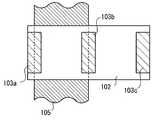
예를 들어, 특허 문헌1에는 도 5a에 도시된 것과 유사한 FET가 개시되어 있고, 즉, 반도체층(102)의 한 쪽 면에 접하여 소스 전극이라 하는 제1 도체 전극(103a)과, 드레인 전극이라 하는 제2 도체 전극(103b)이 구비되고, 반도체층(102)의 다른 쪽의 면에는, 사이에 게이트 절연막(104)을 개재하여, 게이트(105)가 구비된다. 제1 도체 전극(103a)과 제2 도체 전극(103b) 및 게이트(105)용으로 도체가 이용된다.For example,
도 5a에 폭 c로 나타낸 바와 같이, 게이트(105)는 제1 도체 전극(103a)과 겹치는 부분 및 제2 도체 전극(103b)과 겹치는 부분을 갖는 것이 필요하다. 즉, 인용문헌1에서 c가 0보다 큰 것이 필요하다.5A, the
도체 반도체 접합을 이용하여 소스 전극 및 드레인 전극을 형성한 FET에서는, 반도체의 캐리어 농도가 클 때, 오프 상태에서도 소스 전극과 드레인 전극 사이에 전류(오프 전류; off-state current)가 흐른다. 따라서, 반도체의 도너 또는 억셉터의 농도를 감소시켜서, i형 반도체(본 명세서에서는, 도너 또는 억셉터로부터 유도된 캐리어 농도가 1012/㎤이하의 반도체를 i형 반도체라고 함)를 얻도록, 오프 전류를 감소시키는 것이 필요하다.In an FET in which a source electrode and a drain electrode are formed using a conductor semiconductor junction, a current (off-state current) flows between the source electrode and the drain electrode even when the carrier concentration of the semiconductor is large. Therefore, in order to obtain an i-type semiconductor (in this specification, a semiconductor having a carrier concentration of 1012 / cm 3 or less derived from a donor or an acceptor is referred to as an i-type semiconductor) by reducing the concentration of the donor or acceptor of the semiconductor, It is necessary to reduce the off current.
또한, 본 명세서에서는 도너(또는 억셉터)의 농도는, 도너(또는 억셉터)일 수 있는 원소, 화학기 등에 그 이온화율을 곱한 농도이다. 예를 들어, 도너 원소가 2% 포함되어 있고, 그 이온화율이 0.005%이면, 도너 농도는 1ppm(=0.02×0.00005)이다.In the present specification, the concentration of the donor (or acceptor) is a concentration obtained by multiplying the ionization rate by an element such as a donor (or an acceptor), a chemical term, and the like. For example, if the donor element contains 2% and its ionization rate is 0.005%, the donor concentration is 1 ppm (= 0.02 x 0.00005).
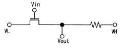
한편, FET를 포함하는 반도체 회로에서, 특히 p 채널형 FET 또는 n 채널형 FET 중 한 쪽을 이용할 수 있는 반도체 회로에서, 기본 회로 중 하나인 인버터는, 예를 들어, 도 6a에 도시한 바와 같이, FET에 저항을 직렬로 접속한 구조를 갖는다.On the other hand, in a semiconductor circuit including an FET, particularly in a semiconductor circuit which can use either a p-channel type FET or an n-channel type FET, an inverter which is one of the basic circuits is, for example, , And a resistor is connected in series to the FET.
이와 달리, 몇몇 경우, 인버터는 도 6b에 도시한 바와 같이, 2개의 FETs를 직렬로 접속하고, FETs(통상은, VH측의 것)의 드레인과 게이트 사이를 단락시켜서, 다이오드를 형성한 구조를 가질 수 있다. 그러나, 도 6b의 인버터는, FET의 드레인과 게이트 사이를 단락시키기 위해 도면에서 X로 표시된 부분에 콘택트를 형성할 필요가 있으므로, 집적도를 높일 수 없는 점에서 단점이 있다.Alternatively, in some cases, the inverter has a structure in which two FETs are connected in series and a diode is formed by short-circuiting the drain and gate of the FETs (normally on the VH side) as shown in FIG. 6B Lt; / RTI > However, the inverter of Fig. 6B has a disadvantage in that it is not possible to increase the degree of integration because it is necessary to form a contact at a portion indicated by X in the figure in order to short-circuit between the drain and the gate of the FET.
도 6a의 타입의 인버터에서는, FET가 온 시의 저항을 RON, FET가 오프시의 저항을 ROFF라고 할 때, RON <<R <<ROFF의 관계를 만족하는 저항값 R을 갖는 저항을 FET에 접속시킨다. 여기서, R은 10RON보다 크고, ROFF/10보다 작은 것이 바람직하고, 더 바람직하게는 R은 100RON보다 크고, ROFF/100보다 작다.In the inverter of the type shown in FIG. 6A, when the FET has a resistance RON when the FET is on and a resistance ROFF when the FET is off, it has a resistance value R satisfying the relation of RON << R << ROFF Connect the resistor to the FET. Here, R is larger than 10 RON , preferably smaller than ROFF / 10, more preferably, R is larger than 100 RON and smaller than ROFF / 100.
이런 타입의 인버터에서는, 입력이 하이(High)이면, 이 저항과 온 상태의 FET를 통해 전류가 흐른다. 이 때, 인버터의 VH와 VL 사이의 저항은, R+RON이다. 만약, 이 관계가 R>>RON이면, 인버터의 저항은 R에 근사할 수 있다. 따라서, 인버터의 전원 전압을 Vdd라고 하면, 소비 전력은, Vdd2/R로 표현될 수 있다. 또한, 출력 전압은 0에 근사할 수 있다.In this type of inverter, if the input is high, current flows through this resistor and the FET on. At this time, the resistance between VH and VL of the inverter is R + RON . If this relationship is R >> RON , the resistance of the inverter can be approximated to R. Therefore, when the power supply voltage Vdd as the inverter, power consumption, and can be represented as Vdd2 / R. In addition, the output voltage can be approximated to zero.
입력이 로우(Low)여도, 이 저항과 FET를 통해 전류가 흐른다. 이 때, 인버터의 저항은, R+ROFF이다. 이 관계가 R <<ROFF이면, 인버터의 저항은 ROFF에 근사할 수 있다. 따라서, 인버터의 소비 전력은, Vdd2/ROFF로 표현될 수 있다. 또한, 출력 전압은 Vdd에 근사할 수 있다.Even if the input is low, current flows through this resistor and the FET. At this time, the resistance of the inverter is R + ROFF . If this relationship is R << ROFF , the resistance of the inverter can be approximated to ROFF . Therefore, the power consumption of the inverter can be expressed as Vdd2 / ROFF . In addition, the output voltage can be approximated to Vdd.
상기의 관계로부터 분명한 바와 같이, R 및 ROFF가 큰 값이면, 소비 전력은 감소될 수 있다. 또한, 출력 전압의 면에서, R이 RON과 ROFF 사이의 중간값인 것이 바람직하고, 이상적으로는, R은 (RON×ROFF)1/2이다. 따라서, ROFF/RON이 큰 값인 것이 바람직하다.As is clear from the above relationship, if R and ROFF are large values, the power consumption can be reduced. In terms of the output voltage, it is preferable that R is an intermediate value between RON and ROFF , and ideally, R is (RON x ROFF )1/2 . Therefore, it is preferable that ROFF / RON is a large value.
종래의 반도체 회로 중에서, p 채널형 FET 또는 n 채널형 FET 중 한 쪽을 이용할 수 있는 반도체 회로로서 아몰퍼스 실리콘 FET를 포함하는 회로가 알려져 있다.Among conventional semiconductor circuits, a circuit including an amorphous silicon FET is known as a semiconductor circuit that can use either a p-channel type FET or an n-channel type FET.
아몰퍼스 실리콘 FET를 포함하는 인버터 회로에서, 저항으로서 n형의 아몰퍼스 실리콘을 이용한다. n형의 아몰퍼스 실리콘은, FET의 소스나 드레인의 재료로서 이용되는 것이며, 아몰퍼스 실리콘의 일부를 가공하여 저항으로 사용한다. n형의 아몰퍼스 실리콘이 높은 저항율을 갖지 않기 때문에, 저항의 크기는 FET의 크기보다 크다.In an inverter circuit including an amorphous silicon FET, n-type amorphous silicon is used as a resistor. The n-type amorphous silicon is used as a material for a source and a drain of an FET, and a part of the amorphous silicon is processed and used as a resistor. Since the n-type amorphous silicon does not have a high resistivity, the resistance is larger than the size of the FET.
한편, 2 전자 볼트 이상의 밴드 갭을 갖는 진성(i형의) 반도체를 이용하여 캐리어 농도를 감소시킨 FET는, 매우 낮은 오프 전류를 갖고, 즉, ROFF가 매우 크고, 또한, 아몰퍼스 실리콘에 비해 상당히 큰 이동도 갖고, 즉, RON이 작고, 따라서, ROFF/RON의 값이 1010이상이다. 이러한 큰 값의 ROFF/RON으로, 저항을 형성 또는 설계시의 마진(margin)이 증가된다.On the other hand, an FET having a reduced carrier concentration using an intrinsic (i-type) semiconductor having a band gap of 2 electron volts or more has a very low off current, that is, ROFF is very large, That is, RON is small, and therefore the value of ROFF / RON is 1010 or more. With such a large value ROFF / RON , the margin for forming or designing a resistance is increased.
그러나, 특허 문헌1 또는 특허 문헌2에서와 같이, 반도체에 직접 도체를 접속시킨 FETs에서는, 아몰퍼스 실리콘을 포함하는 FET의 경우와 달리, 저항에 적당한 재료를 발견할 수 없다. 특히, 캐리어 농도의 감소를 통해 형성된 i형의 반도체는 매우 높은 저항율을 갖는다고 여겨지기 때문에, 저항에 i형의 반도체를 사용하는 것이 전혀 상정되지 않는다.However, unlike the case of FETs including amorphous silicon, it is impossible to find a material suitable for resistance in FETs in which a conductor is directly connected to a semiconductor, as in
본 발명은, 상술한 바와 같이 도체 반도체 접합을 갖는 FET의 회로 설계를 고안함으로써 우수한 FET, 반도체 장치, 또는 반도체 회로, 또는 그 제작 방법을 제공하는 것을 목적으로 한다. 또한, 도체 반도체 접합의 특성을 이용함으로써, 우수한 특성을 나타내는 FET 또는 반도체 장치, 또는 그 제작 방법을 제공하는 것을 목적으로 한다. 또한, 용이한 가공을 통해 제조될 수 있는 FET 또는 반도체 장치, 또는 그 제작 방법을 제공하는 것을 목적으로 한다. 또한, 집적도가 높은 FET 또는 반도체 장치, 또는 그 제작 방법을 제공하는 것을 다른 목적으로 한다. 본 발명은 상기 목적 중 적어도 하나를 해결한다.It is an object of the present invention to provide an excellent FET, a semiconductor device, or a semiconductor circuit, or a manufacturing method thereof by devising a circuit design of an FET having a conductor semiconductor junction as described above. It is also an object of the present invention to provide an FET or a semiconductor device exhibiting excellent characteristics by using the characteristic of the conductor semiconductor junction, or a method of manufacturing the same. It is also an object of the present invention to provide an FET or a semiconductor device which can be manufactured through easy machining, or a manufacturing method thereof. It is another object of the present invention to provide an FET or a semiconductor device having a high degree of integration, or a manufacturing method thereof. The present invention solves at least one of the above objects.
본 발명을 설명하기 전에, 본 명세서에서 이용하는 용어에 대하여 간단히 설명한다. 우선, 본 명세서에서의 트랜지스터의 소스와 드레인에 대하여, n 채널형 FET에서는 높은 전위가 제공되는 단자를 드레인, 다른 단자를 소스라고 하고, p 채널형 FET에서는 낮은 전위가 제공되는 단자를 드레인, 다른 단자를 소스라고 한다. 2개의 단자에 동일 전위를 공급하는 경우, 어느 한 쪽을 소스, 다른 쪽을 드레인이라고 한다.Before describing the present invention, the terms used in this specification will be briefly described. First of all, with respect to the source and the drain of the transistor in this specification, a terminal provided with a high potential in an n-channel type FET is referred to as a drain and the other terminal is referred to as a source and a terminal provided with a low potential in a p- The terminal is called the source. When the same potential is supplied to two terminals, one is called a source and the other is called a drain.
"소스 전극", "드레인 전극"이라고 하는 용어 대신에, 이러한 부분을 "제1 도체 전극", "제2 도체 전극"으로 하는 경우도 있다. 그 경우는, 전위 레벨에 따라 이러한 부분 사이의 명칭을 변경하지 않는다.Instead of the terms "source electrode" and "drain electrode", these portions may be referred to as "first conductor electrode" and "second conductor electrode". In that case, the name between these parts is not changed according to the potential level.
본 발명의 제1 실시 형태는, 반도체층과, 반도체층의 한 쪽 면에 접하여 구비된 제1 도체 전극 및 제2 도체 전극과, 반도체층의 다른 쪽의 면에 구비된 게이트를 포함하는 FET이다. 제1 도체 전극과 게이트 사이 및 제2 도체 전극과 게이트 사이의 적어도 한 쪽 영역에 오프셋 영역이 형성된다.A first embodiment of the present invention is an FET including a semiconductor layer, a first conductor electrode and a second conductor electrode provided in contact with one surface of the semiconductor layer, and a gate provided on the other surface of the semiconductor layer . An offset region is formed in at least one region between the first conductor electrode and the gate and between the second conductor electrode and the gate.
본 발명의 제2 실시 형태는, 반도체층과, 반도체층의 한 쪽 면에 접하여 구비된 제1 도체 전극 및 제2 도체 전극과, 동일한 면에 구비된 게이트를 포함하는 FET이다. 제1 도체 전극과 게이트 사이 및 제2 도체 전극과 게이트 사이의 적어도 한 쪽 영역에 오프셋 영역이 형성된다.A second embodiment of the present invention is an FET including a semiconductor layer, first and second conductor electrodes provided in contact with one surface of the semiconductor layer, and a gate provided on the same surface. An offset region is formed in at least one region between the first conductor electrode and the gate and between the second conductor electrode and the gate.
상기의 본 발명의 제1 및 제2 실시 형태에서, 오프셋 영역의 폭은, 10nm 이상 100nm 이하, 바람직하게는 10nm 이상 50nm 이하, 보다 바람직하게는 10nm 이상 20nm 이하이다. 또한, 반도체층의 두께는, 바람직하게 오프셋 영역의 폭 이하, 더 바람직하게는, 오프셋 영역의 폭의 절반 이하이다. 또한, 게이트의 폭은, 바람직하게 오프셋 영역의 폭 이상이면 좋다.In the first and second embodiments of the present invention, the width of the offset region is 10 nm or more and 100 nm or less, preferably 10 nm or more and 50 nm or less, and more preferably 10 nm or more and 20 nm or less. Further, the thickness of the semiconductor layer is preferably not more than the width of the offset region, more preferably not more than half the width of the offset region. The width of the gate may preferably be equal to or larger than the width of the offset region.
본 발명의 제3 실시 형태는, 반도체층과, 반도체층의 한 쪽 면에 접하여 구비된 제1 도체 전극, 제2 도체 전극 및 제3 도체 전극과, 반도체층의 다른 쪽의 면에 구비된 게이트를 갖는 반도체 장치이다.A third embodiment of the present invention is a semiconductor device including a semiconductor layer, a first conductor electrode, a second conductor electrode and a third conductor electrode provided in contact with one surface of the semiconductor layer, and a gate electrode provided on the other surface of the semiconductor layer .
본 발명의 제4 실시 형태는, 반도체층과, 반도체층의 한 쪽 면에 접하여 구비된 제1 도체 전극, 제2 도체 전극 및 제3 도체 전극과, 동일한 면에 구비된 게이트를 갖는 반도체 장치이다.A fourth embodiment of the present invention is a semiconductor device having a semiconductor layer, a first conductive electrode, a second conductive electrode and a third conductive electrode provided in contact with one surface of the semiconductor layer, and a gate provided on the same surface .
상기 본 발명의 제1 내지 제4 실시 형태에서, 제1 내지 제3 도체 전극의 반도체층에 접하는 부분의 일함수는, 반도체층의 전자 친화력과 0.3 전자 볼트의 합(즉, 전자 친화력+0.3 전자 볼트)보다 작은 것이 바람직하다. 이와 달리, 제1 도체 전극 및 제2 도체 전극과 반도체층 사이에 오믹 접합이 형성되는 것이 바람직하다.In the first to fourth embodiments of the present invention, the work function of the portion of the first to third conductor electrodes in contact with the semiconductor layer is determined by the sum of the electron affinity of the semiconductor layer and 0.3 electron volts (i.e., the electron affinity + Bolts). Alternatively, an ohmic contact may be formed between the first and second conductive electrodes and the semiconductor layer.
상기 본 발명의 제1 내지 제4 실시 형태에서, 게이트의, 반도체층에 가장 가까운 부분의 재료의 일함수는, 반도체층의 전자 친화력과 0.6 전자 볼트의 합(즉, 전자 친화력+0.6 전자 볼트)보다 큰 것이 바람직하다. 또한, 반도체층은 i형 반도체층인 것이 바람직하다.In the first to fourth embodiments of the present invention, the work function of the material closest to the semiconductor layer of the gate is the electron affinity of the semiconductor layer and the sum of 0.6 electron volts (i.e., the electron affinity +0.6 electron volts) . The semiconductor layer is preferably an i-type semiconductor layer.
상기 본 발명의 제1 내지 제4 실시 형태에서, FET 또는 반도체 회로는, 적절한 기판 위에 구비될 수 있다. 이 경우, 게이트와 기판 사이에 반도체층을 구비하는 구성, 또는, 반도체층과 기판 사이에 게이트를 구비하는 구성을 채용할 수 있다.In the first to fourth embodiments of the present invention, the FET or the semiconductor circuit may be provided on a suitable substrate. In this case, the semiconductor layer may be provided between the gate and the substrate, or a gate may be provided between the semiconductor layer and the substrate.
기판의 재료의 예로서는, 단결정 실리콘 등의 반도체, 각종 글래스, 석영, 사파이어, 각종 세라믹스 등의 절연체, 알루미늄, 스테인리스 강, 구리 등의 도체 등을 들 수 있다. 반도체나 도체를 기판으로서 이용하는 경우, 기판의 표면에 절연층을 구비하는 것이 바람직하다.Examples of the material of the substrate include semiconductors such as single crystal silicon, various glass, quartz, sapphire, insulators such as various ceramics, and conductors such as aluminum, stainless steel, and copper. When a semiconductor or a conductor is used as a substrate, it is preferable to provide an insulating layer on the surface of the substrate.
또한, 반도체층과 게이트 사이에는 게이트 절연막을 구비하여도 된다. 또는, 반도체층과 게이트 사이에 쇼트키 배리어 접합이 형성될 수 있다. 또한, 제1 내지 제3 도체 전극은 모두 같은 재료로 구성될 필요는 없다. 제1 내지 제3 도체 전극 각각이 상이한 재료로 형성될 수 있고, 또는 그들 중 2개가 같은 재료로 형성될 수 있다.A gate insulating film may be provided between the semiconductor layer and the gate. Alternatively, a Schottky barrier junction may be formed between the semiconductor layer and the gate. Further, the first to third conductor electrodes are not necessarily made of the same material. Each of the first to third conductor electrodes may be formed of different materials, or two of them may be formed of the same material.
또한, 반도체층의 종류는, 산화물에 한정되지 않고, 황화물 등의 II-VI족 화합물을 사용할 수 있다. 또한, 상술한 바와 같이 열적 여기에 의해 생성된 캐리어를 줄이기 위해, 반도체의 밴드 갭은 2 전자 볼트 이상 4 전자 볼트 미만이 바람직하고, 더 바람직하게는, 2.9 전자 볼트 이상 3.5 전자 볼트 미만이다.The type of the semiconductor layer is not limited to an oxide, but a II-VI group compound such as a sulfide may be used. Further, in order to reduce the carrier generated by the thermal excitation as described above, the band gap of the semiconductor is preferably 2 electron volts or more and less than 4 electron volts, and more preferably 2.9 electron volts or more and less than 3.5 electron volts.
상기의 구성 중 어느 하나를 채용함으로써, 상기 목적의 적어도 하나를 해결할 수 있다. 본 발명에서, 도체 반도체 접합의 특성을 이용하여, 적절한 저항 영역을 형성하고, 이 저항 영역은 FET의 오프셋 영역, 반도체 회로 또는 반도체 장치를 형성하는데 이용된다.By adopting any one of the above constructions, at least one of the above objects can be solved. In the present invention, by using the characteristic of the conductor semiconductor junction, an appropriate resistance region is formed, and this resistance region is used to form an offset region of the FET, a semiconductor circuit or a semiconductor device.
특허 문헌1 또는 특허 문헌2에 개시된 바와 같은 FET에서는, 소스 전극, 드레인 전극 및 게이트는 도체로 형성된다. 그러나, 반도체에 대한 도체의 영향에 대하여는, 지금까지 충분히 고려되지 않고 있었다.In the FET as disclosed in
이러한 점에서, 본 발명자의 고찰에 의하면, 도체 반도체 접합에서, 도체의 일함수가 반도체층의 전자 친화력보다 작은 경우, 반도체층에 전자가 유입하여, 오믹 접합이 형성되는 것을 발견하였다.In this regard, the inventors of the present invention have found that when the work function of the conductor is smaller than the electron affinity of the semiconductor layer in the conductor semiconductor junction, electrons flow into the semiconductor layer to form an ohmic junction.
FET에서, 소스 전극과 반도체 또는 드레인 전극과 반도체 사이의 접합은, 전류가 흐르기 쉬운 것이 바람직하므로, 오믹 접합이 형성되도록 소스 전극 또는 드레인 전극의 재료가 선택된다. 예를 들어, 티타늄 및 질화 티타늄이 제공된다. 전극과 반도체 사이의 접합이 오믹 접합이면, 얻어지는 FET의 특성이 안정되고, 양품율이 높아지는 장점이 있다.In the FET, since the junction between the source electrode and the semiconductor or the drain electrode and the semiconductor is preferably easy to flow, the material of the source electrode or the drain electrode is selected so that the ohmic junction is formed. For example, titanium and titanium nitride are provided. If the junction between the electrode and the semiconductor is an ohmic contact, the characteristics of the obtained FET are stabilized and the yield of the product is increased.
이러한 도체 반도체 접합에서, 도체에 가까운 영역에서 전자의 농도가 높고, 전자 농도는, 도체 반도체 접합의 계면으로부터 수 nm에서는 1020/㎤, 몇 십 nm에서는 1018/㎤, 몇 백 nm에서는 1016/㎤, 수 마이크로미터에서도 1014/㎤가 되는 것으로 대략적으로 계산된다. 즉, 반도체 자체가 진성(i형)이어도, 도체와의 접촉에 의해, 캐리어 농도가 높은 영역이 형성된다. 높은 캐리어 농도를 가진 영역이 도체 반도체 접합의 계면 근방에 형성되는 것에 의해, 도체 반도체 접합은 오믹 접합이 될 수 있다.In this conductive semiconductor junction, a high electron density in the region close to the conductor, the electron density is, the number from the interface of the conductive semiconductor junction nm 1020 / ㎤, in the several tens of nm 1018 / ㎤, a few hundred nm 1016 / Cm < 3 > and 1014 / cm < 3 > at several micrometers. That is, even if the semiconductor itself is intrinsic (i-type), a region having a high carrier concentration is formed by contact with the conductor. Since the region having a high carrier concentration is formed in the vicinity of the interface of the conductor semiconductor junction, the conductor semiconductor junction can be an ohmic junction.
또한, 게이트의 재료로서, 반도체층의 일함수보다 큰 전자 친화력을 가진 도체를 이용하면, 게이트는 반도체에서 전자를 제거하는 작용을 갖는 것도 분명해진다. 예를 들어, 텅스텐 및 백금을 게이트 재료의 예로 들 수 있다. 이러한 재료를 이용함으로써, 오프 전류를 매우 작게 할 수 있는 것을 알았다.Further, when a conductor having an electron affinity greater than the work function of the semiconductor layer is used as the material of the gate, it is also apparent that the gate has an action of removing electrons from the semiconductor. For example, tungsten and platinum are examples of gate materials. It has been found that by using such a material, the off current can be made very small.
상기의 고찰을 기초로 하면, 도 5a에 도시되는 FET의 반도체층(102)에서의, 제1 도체 전극(103a), 제2 도체 전극(103b), 게이트(105)가 동일 전위를 가질 경우의, 캐리어 농도의 개념적 분포는 도 5b에 도시된다. 여기서, 제1 도체 전극(103a), 제2 도체 전극(103b) 각각의 일함수를 Wm, 게이트(105)의 일함수를 Wg, 반도체층(102)의 전자 친화력을 φ로 했을 때, Wm <φ+0.3 전자 볼트, Wg>φ+0.6 전자 볼트라고 하는 조건을 충족시킨다.On the basis of the above consideration, it is considered that when the
도 5b에 도시된 바와 같이, 제1 도체 전극(103a), 제2 도체 전극(103b)으로부터 전자가 주입되고, 제1 도체 전극(103a), 제2 도체 전극(103b)의 근방은, 매우 전자 농도가 높은 영역(102a)을 형성한다. 게이트(105)에 가까운 부분에, 전자 농도가 매우 낮은 영역(102e)이 형성된다. 영역(102a)과 영역(102e) 사이에, 전자 농도는, 제1 도체 전극(103a), 제2 도체 전극(103b)으로부터 더 떨어진 부분 또는 게이트(105)에 근접한 영역에서 낮아진다.5B, electrons are injected from the
도 5b는, 영역(102b)의 전자 농도가 영역(102a)의 전자 농도보다 약 1자리(an order of magnitude) 정도 낮고, 영역(102c)의 전자 농도가 영역(102b)의 전자 농도보다 약 1자리 정도 낮고, 영역(102d)의 전자 농도가 영역(102c)의 전자 농도보다 약 1자리 정도 낮게 도시된다. 전자 농도가 높을수록 도전성이 높아진다. 반대로, 전자 농도가 낮아질수록, 도전성이 저하된다. 예를 들어, 영역(102e)에서의 반도체층(102)은 절연체이다.5B shows that the electron concentration of the
도 5b에 도시되는 FET의 오프 전류는, 제1 도체 전극(103a)과 제2 도체 전극(103b) 사이의 중간 영역에 형성되는 영역(102e)에 의해 결정된다. 한편, 제1 도체 전극(103a)과 게이트(105)가 서로 겹치는 부분, 제2 도체 전극(103b)과 게이트(105)가 서로 겹치는 부분, 및 이 부분들의 주변 영역은, 오프 전류의 감소에 거의 영향을 미치지 않는 것을 알았다.The off current of the FET shown in Fig. 5B is determined by the
도 5a에 도시되는 FET에서 제1 도체 전극(103a)과 제2 도체 전극(103b)의 간격을 좁히면, 영역(102e)이 좁아지고, 영역(102e)보다 전자 농도가 높은 영역이 넓어진다. 이 상태는, 오프 전류가 증대하기 때문에 바람직하지 않다. 따라서, 제1 도체 전극(103a)과 제2 도체 전극(103b) 사이의 간격은, 오프 전류를 일정한 값 이하로 하기 위해, 어떤 값을 유지할 필요가 있다.When the distance between the
본 발명자는, 도 5b에 도시한 바와 같은 전자 농도 분포는, 도 5a의 구조 이외의, 예를 들어, 도 1a에 도시한 바와 같은 구조에서도 얻어질 수 있다는 것을 알았다. 도 1a에 도시된 구조의 FET에서, 제1 도체 전극(103a), 제2 도체 전극(103b)이 게이트(105)와 중첩되지 않도록 구비된다. 도 1a에서, 제1 도체 전극(103a)과 게이트(105) 사이에, 폭 d의 오프셋 영역이 구비된다.The present inventors have found that the electron concentration distribution as shown in Fig. 5B can be obtained in a structure other than the structure of Fig. 5A, for example, as shown in Fig. 1A. In the FET of the structure shown in FIG. 1A, the
도 1a에 도시된 FET는 적절한 재료의 기판 위에 구비될 수 있다. 이 경우, 기판은 도면에서 게이트(105) 위 또는 제1 도체 전극(103a) 아래에 위치될 수 있다.The FET shown in Fig. 1A may be provided on a substrate of suitable material. In this case, the substrate may be positioned on the
통상, 이와 같은 오프셋 영역은 FET에 직렬로 저항을 접속할 경우와 같은 효과를 제공할 수 있다. 그러나, 본 발명자의 고찰에 의하면, 이러한 오프셋 영역을 구비해도, d가 100nm 이하, 바람직하게는 50nm 이하, 보다 바람직하게는 20nm 이하이면, FET의 동작에 미치는 영향은 경미한 것이 분명해졌다.Normally, such an offset region can provide the same effect as when a resistor is connected in series to the FET. However, according to the investigation by the inventors of the present invention, even if such an offset region is provided, it has become clear that the effect on the operation of the FET is small if d is 100 nm or less, preferably 50 nm or less, more preferably 20 nm or less.
이는, 상기에 설명한 바와 같이, 제1 도체 전극(103a), 제2 도체 전극(103b)으로부터 반도체층(102)에 전자가 유입되어, 전자 농도의 높은 부분(예를 들어, 영역(102c))이 오프셋 영역에도 형성되기 때문이다. n 채널형 FET의 경우, 게이트(105)에 플러스의 전위를 인가하면, 도 1b의 영역(102e), 영역(102d)의 오프셋 영역 바로 아래에 있는 부분은 전자 농도가 높은 영역이 되고, 제1 도체 전극(103a)과 제2 도체 전극(103b)을 연결하는 경로가 형성된다.This is because electrons flow into the
이와 같은 구조로 하면, 게이트(105)와 제1 도체 전극(103a) 사이와, 게이트(105)와 제2 도체 전극(103b) 사이의 기생 용량을 충분히 저감시킬 수 있다. 이 효과를 얻기 위해, 오프셋 영역의 폭 d는 10nm 이상인 것이 바람직하다. 오프셋 영역의 폭 d가 10nm 미만에서는, 게이트(105)와 제1 도체 전극(103a) 사이 또는 게이트(105)와 제2 도체 전극(103b) 사이의 기생 용량이 현저하게 증가한다.With this structure, the parasitic capacitance between the
도 1a에 도시되는 FET에서, 제1 도체 전극(103a)과 제2 도체 전극(103b)은 게이트(105)가 구비된 면과 다른 면에 구비된다. 게이트(105)가 구비되는 동일 면에 제1 도체 전극(103a)과 제2 도체 전극(103b)이 구비되는 FET도 제작할 수 있다.In the FET shown in Fig. 1A, the
도 1c는 반도체층(102)의 동일한 면 위에 제1 도체 전극(103a), 제2 도체 전극(103b), 게이트 절연막(104) 및 게이트(105)가 구비된 FET를 도시한다. 게이트(105)와 제1 도체 전극(103a) 사이, 및 게이트(105)와 제2 도체 전극(103b) 사이에는 오프셋 영역을 구비한다.1C shows an FET having a
반도체층(102)은, 제1 도체 전극(103a)과 제2 도체 전극(103b)을 접촉시킴으로써, 전자가 공급되어, 도 1c에 도시한 바와 같이, 전자 농도가 다양한 영역이 형성된다. 전자 농도의 분포는, 제1 도체 전극(103a)과 제2 도체 전극(103b)이 게이트(105)가 구비된 동일 면에 구비되기 때문에, 도 1b와는 약간 상이하다.Electrons are supplied to the
도 1c의 구조에서는, 특히, 반도체층(102)의 게이트로부터의 반대측에, 제1 도체 전극(103a)과 제2 도체 전극(103b)의 영향력이 상대적으로 저하되기 때문에, 그 부분의 전자 농도가, 도 1b의 구조에 비해 저하된다. 그 결과, 오프 전류가 더 적어진다.1C, the influence of the
이러한 구조의 FET는, 종래 실리콘 MOSFET와 유사한 구조이기 때문에, 다층 배선 등의 프로세스를 도 1a의 구조보다 간편하게 할 수 있고, 집적도를 높일 수 있는 이점이 있다. 또한, 종래 실리콘 MOSFET의 경우, 필요한 이온 주입을 이용한 도핑 프로세스가 도 1c의 구조에서는 불필요하다. 즉, 게이트를 구비한 부분은 자동적으로 전자 농도가 매우 낮은 채널로 작용하고, 그 밖의 부분은 적절한 전자 농도를 가진 익스텐션 영역에 상당한다.Since the FET having such a structure has a structure similar to that of the conventional silicon MOSFET, the process of the multilayer wiring or the like can be made simpler than the structure of FIG. 1A, and the integration degree can be increased. Further, in the case of the conventional silicon MOSFET, the doping process using necessary ion implantation is unnecessary in the structure of FIG. 1C. That is, the portion having the gate functions automatically as a channel with a very low electron concentration, and the other portion corresponds to the extension region having an appropriate electron concentration.
제1 도체 전극(103a), 제2 도체 전극(103b)으로부터 반도체층(102)에 전자가 유입하고, 적절한 전자 농도를 가진 부분이 형성되고, 이는 이러한 적절한 전자 농도를 가진 부분이 온 상태의 FET의 저항값과 오프 상태의 FET의 저항값 사이의 중간의 저항값을 갖는 것을 의미한다.Electrons flow into the
도 5a 내지 도 5c로 복귀해서, 도 5a의 FET로부터 게이트(105)를 제거한 경우의 반도체층(102)의 캐리어 농도의 개념적 분포는 도 5c에 도시된다. 이 경우, 전자를 제거하는 게이트의 작용을 얻을 수 없고, 이는 제1 도체 전극(103a), 제2 도체 전극(103b)으로부터 주입된 전자에 의해, 전자 농도가 높은 영역이 도 5b의 것보다 넓게 형성된다.Returning to Figs. 5A to 5C, the conceptual distribution of the carrier concentration of the
도 5b의 FET는 오프 상태이며, FET의 온 상태에서 게이트(105)에 의해, 반도체층(102)의 넓은 영역에 전자 농도가 높은 영역이 형성되는 사실을 고려하면, 도 5c는 온 상태와 오프 상태 사이의 중간 상태에서의 FET를 도시한다.Considering the fact that the FET of FIG. 5B is in an OFF state and a region having a high electron concentration is formed in a wide region of the
이러한 상태에서의 저항값(제1 도체 전극(103a)과 제2 도체 전극(103b) 사이 영역의 저항값)도 온 상태의 FET의 저항값과 오프 상태의 FET의 저항값 사이의 중간의 저항값을 갖는다. 이 저항값은, 캐리어 농도에 반비례한다. 도 5a의 FET로부터 게이트(105)를 제거한 구조의 소자(이하, 저항 소자라고 함)의 반도체층의 저항율은, 같은 두께의 반도체층을 포함하는 오프 상태의 FET의 반도체층의 저항율보다 3 내지 8자리만큼 낮다.The resistance value in this state (the resistance value of the area between the
이러한 저항 소자는, 상기에서 설명한 바와 같이, 도 6a에 도시되는 인버터의 저항으로서 이용하는 것이 바람직하다. 특히, 제1 도체 전극(103a)과 제2 도체 전극(103b) 사이의 간격 L을 100nm 이상 10μm 이하로 할 때, 간격 L과 대략 동일한 채널 길이(L의 1/2 이상 5배 이하의 채널 길이)를 갖고, 온 저항 RON, 오프 저항ROFF를 갖는 FET를 이용하는 가정 하에, RON <<R <<ROFF인 관계를 충족시킬 수 있다.Such a resistance element is preferably used as the resistance of the inverter shown in Fig. 6A, as described above. Particularly, when the interval L between the
이 때, FET의 채널 폭은 저항 소자 폭의 50% 이상 200%이하, FET의 반도체층의 두께는 저항 소자의 반도체층 두께의 50% 이상 200% 이하로 하면 좋다. 물론, 그 이외의 조건에서 상기 관계를 충족시키는 것은 가능하다.At this time, the channel width of the FET may be 50% or more and 200% or less of the width of the resistance element, and the thickness of the semiconductor layer of the FET may be 50% or more and 200% or less of the thickness of the semiconductor layer of the resistance element. Of course, it is possible to satisfy the above relationship under other conditions.
상기의 설명에서, 도체의 일함수에 대하여 논의한다. 가장 간단한 가정으로, 도체의 일함수는 반도체와의 계면에 의해 결정되는 값일 수 있고, 실제로 계면에서 화학적 반응에 의해 반도체와 도체의 화합물이 생성되거나, 전하나 이종 원소가 트랩되는 등의 복잡한 물성이 종종 관찰된다.In the above description, the work function of the conductor is discussed. In the simplest assumption, the work function of the conductor can be a value determined by the interface with the semiconductor, and complex physical properties such as a compound of a semiconductor and a conductor are generated by a chemical reaction at the interface, Often observed.
예를 들어, 반도체층 위에 두께가 수 나노미터 이하의 매우 얇은 제1 도체층과, 비교적 큰 두께를 가진 제2 도체층이 이 순서대로 적층되어 있는 경우, 제1 도체층의 일함수의 영향이 상당히 저하된다. 따라서, 본 발명을 적용할 때, 반도체층을 가진 계면으로부터 5nm 떨어진 위치에서의 각각의 재료의 일함수 등이 본 발명의 바람직한 조건을 충족시키도록 설계될 수 있다.For example, in the case where a very thin first conductor layer having a thickness of several nanometers or less and a second conductor layer having a relatively large thickness are stacked on the semiconductor layer in this order, the influence of the work function of the first conductor layer . Therefore, when the present invention is applied, the work function of each material at a position 5 nm from the interface with the semiconductor layer, etc. can be designed to satisfy the preferable conditions of the present invention.
본 발명은, 캐리어로서, 실질적으로 전자와 정공 중 한 쪽이 이용될 수 있는 반도체 재료에 대해 특히 효과적이다. 즉, 전자와 정공 중 한 쪽의 이동도가 1㎠/Vs인 반면, 다른 쪽의 이동도가 0.01㎠/Vs이하이거나, 전자 및 정공 중 다른 쪽이 캐리어로서 존재하지 않거나, 전자 및 정공 중 다른 쪽의 유효 질량이 자유 전자의 유효 질량보다 100배 이상인 경우, 본 발명에 따라 바람직한 결과를 얻을 수 있다.The present invention is particularly effective as a carrier for a semiconductor material in which one of electrons and holes can be used. That is, the mobility of one of the electron and the hole is 1 cm 2 / Vs, while the other mobility is 0.01 cm 2 / Vs or less, or the other of the electron and the hole is not present as a carrier, When the effective mass of the free electrons is 100 times or more than the effective mass of the free electrons, preferable results can be obtained according to the present invention.
첨부된 도면에서,
도 1a 내지 도 1c는 본 발명의 전계 효과 트랜지스터의 동작 원리를 도시한다.
도 2a 내지 도 2c는 본 발명의 반도체 회로의 예를 도시한다.
도 3a 내지 도 3c는 본 발명의 반도체 회로의 예를 도시한다.
도 4a 내지 도 4d는 본 발명의 반도체 회로의 제작 공정의 예를 도시한다.
도 5a 내지 도 5c는 본 발명의 원리를 설명한다.
도 6a 및 도 6b는 종래의 인버터 회로도이다.In the accompanying drawings,
1A to 1C show the operation principle of the field effect transistor of the present invention.
2A to 2C show an example of a semiconductor circuit of the present invention.
3A to 3C show examples of the semiconductor circuit of the present invention.
4A to 4D show an example of a manufacturing process of a semiconductor circuit of the present invention.
Figures 5A-5C illustrate the principles of the present invention.
6A and 6B are circuit diagrams of a conventional inverter.
이하, 실시 형태에 대하여 도면을 참조하여 설명한다. 실시 형태는 많은 다른 형태로 실시하는 것이 가능하며, 본 발명의 기술사상 및 범위 내에서 그 형태 및 상세를 여러가지로 변경할 수 있는 것은 당업자라면 용이하게 이해한다. 따라서, 본 발명은 본 실시 형태의 기재 내용에 한정하여 해석되는 것은 아니다. 또한, 이하에 설명하는 구성에서, 동일 부분 또는 유사한 기능을 갖는 부분은 다른 도면에 동일 참조 번호로 표시하고, 그 부분의 상세한 설명은 반복되지 않는다.Hereinafter, embodiments will be described with reference to the drawings. It is to be understood by those skilled in the art that the embodiments can be embodied in many different forms and that various changes in form and details may be made therein without departing from the spirit and scope of the invention. Therefore, the present invention is not construed as being limited to the description of the present embodiment. In the structures described below, parts having the same or similar functions are denoted by the same reference numerals in the other drawings, and detailed description thereof will not be repeated.
(제1 실시 형태)(First Embodiment)
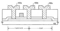
본 실시 형태에서는, 도 2a 내지 도 2c에 도시하는 반도체 회로에 대하여 설명한다. 도 2a는 반도체 회로의 단면의 개념도, 도 2b는, 도 2a의 하측으로부터 본 반도체 회로를 도시한다. 이 반도체 회로는, 도 2a에 도시한 바와 같이, 반도체층(102)의 한 쪽 면에 접한, 제1 도체 전극(103a), 제2 도체 전극(103b), 제3 도체 전극(103c)을 갖는다. 반도체층(102)의 다른 쪽의 면에는 게이트(105)를 구비한다. 게이트(105)와 반도체층(102) 사이에는 게이트 절연막(104)을 구비한다.In the present embodiment, the semiconductor circuit shown in Figs. 2A to 2C will be described. FIG. 2A is a conceptual view of a section of a semiconductor circuit, and FIG. 2B shows a semiconductor circuit viewed from the lower side of FIG. 2A. 2A, the semiconductor circuit has a
기판은, 제1 도체 전극(103a), 제2 도체 전극(103b), 제3 도체 전극(103c) 아래 중 하나에 또는 게이트(105) 위에 구비하여도 된다. 또한, 이 반도체 회로의 반도체층(102)은, 도 2b에 도시한 바와 같이, 대략 직사각형 형상이고, 제1 도체 전극(103a), 제2 도체 전극(103b), 제3 도체 전극(103c)이 구비된다. 또한, 반도체층(102)은 i형 반도체로 형성되고, 바람직하게는 반도체의 밴드 갭이 2 전자 볼트 이상 4 전자 볼트 미만, 더 바람직하게는, 2.9 전자 볼트 이상 3.5 전자 볼트 미만이면 좋다.The substrate may be provided on one of the
게이트(105)는, 반도체층(102)의 제1 도체 전극(103a)과 제2 도체 전극(103b) 사이의 영역(이 영역은 제1 도체 전극(103a)과 제2 도체 전극(103b)이 중첩되는 부분을 포함하지 않는다)과 중첩하도록 구비되지만, 반도체층(102)의 제2 도체 전극(103b)과 제3 도체 전극(103c) 사이의 영역(이 영역은 제2 도체 전극(103b)과 제3 도체 전극(103c)이 중첩되는 부분을 포함하지 않는다)과는 중첩되지 않도록 구비된다.The
이러한 구조로 함으로써, 제1 도체 전극(103a), 제2 도체 전극(103b), 게이트(105) 및 제1 도체 전극(103a), 제2 도체 전극(103b), 게이트(105)에 의해 둘러싸여진 반도체층(102)은 FET를 형성한다. 또한, 제2 도체 전극(103b)과 제3 도체 전극(103c), 및 제2 도체 전극(103b)과 제3 도체 전극(103c) 사이의 반도체층(102)의 부분은 저항을 형성한다.With this structure, the
즉, 도 2a에 도시한 바와 같이, 전자(the former)가 트랜지스터부로서 기능하고, 후자가 저항부로서 기능한다. 반도체층(102)의 트랜지스터부와 저항부에서의 전자 농도의 분포는, 각각 도 5b에 도시된 분포 및 도 5c에서 도시된 분포와 거의 동일하다. 따라서, 도 2c의 회로도에 도시된 바와 같이, 도 6a의 타입의 인버터가 얻어진다.That is, as shown in FIG. 2A, the former functions as a transistor portion, and the latter functions as a resistance portion. The distribution of the electron concentration in the transistor portion and the resistive portion of the
또한, 도 2b에 도시된 바와 같이, 트랜지스터부의 채널 폭 방향의 길이와, 채널 폭 방향에 대응하는 방향의 저항부의 길이는 대략 동일하다. 도 2a 내지 도 2c의 구조를 가진 인버터가 도 6b에 도시된 인버터보다 높은 집적도를 갖는 것은 이하의 이유로부터도 분명하다.2B, the length of the transistor portion in the channel width direction and the length of the resistor portion in the direction corresponding to the channel width direction are substantially the same. The inverter having the structure of FIGS. 2A to 2C has a higher integration degree than the inverter shown in FIG. 6B is also apparent from the following reason.
예를 들어, 동일한 방식으로 도 6b의 타입의 인버터를 형성할 때, 제2 도체 전극(103b)과 제3 도체 전극(103c) 사이에도 게이트를 구비할 필요가 있다. 그러나, 게이트(105)와 게이트(105)에 인접한 게이트 사이의 절연을 보장하기 위해, 최소 가공 선 폭 이상의 간격을 인접한 게이트들 사이에 설정할 필요가 있다. 그 결과, 제2 도체 전극(103b)의 폭을 넓게 할 필요가 있다.For example, when the inverter of the type shown in FIG. 6B is formed in the same manner, it is necessary to provide a gate between the
도 2a 및 도 2b에서, 최소 가공 선 폭은, 제1 도체 전극(103a), 제2 도체 전극(103b) 또는 제3 도체 전극(103c)의 폭이다. 따라서, 도 6b의 타입의 인버터에서, 제2 도체 전극(103b)의 폭은 도 2a 및 도 2b에서의 2배의 폭을 필요로 한다. 반대로, 도 6a의 타입의 인버터에서는, 제2 도체 전극(103b)과 제3 도체 전극(103c) 사이에 게이트를 구비할 필요가 없으므로, 제2 도체 전극(103b)의 폭을 최소 선 폭으로 설정할 수 있다.2A and 2B, the minimum line width is the width of the
도 2a 내지 도 2c에 도시된 바와 같은 반도체 장치는 다음의 방법으로 제작될 수 있고, 즉, 제1 도체 전극(103a), 제2 도체 전극(103b) 및 제3 도체 전극(103c)을 기판 위에 형성하고, 그 후, 반도체층(102), 게이트 절연막(104) 및 게이트(105)를 형성한다.2A to 2C can be manufactured by the following method. That is, the
이와 달리, 다음 방법을 채용할 수 있고, 즉, 기판 위에 게이트(105)를 형성하고, 그 후, 게이트 절연막(104), 반도체층(102), 제1 도체 전극(103a), 제2 도체 전극(103b) 및 제3 도체 전극(103c)을 형성한다.Alternatively, the
또한, 도 2a 내지 도 2c에서는, 제1 도체 전극(103a)과 제2 도체 전극(103b)사이의 간격, 제2 도체 전극(103b)과 제3 도체 전극(103c) 사이의 간격을 대략 동일하게 했지만, 전자(the former)의 간격을 후자의 간격보다 크게 또는 작게 설정할 수 있다.2A to 2C, the interval between the
(제2 실시 형태)(Second Embodiment)
본 실시 형태에서, 도 3a 내지 도 3c에 도시하는 반도체 회로에 대하여 설명한다. 도 3a는 반도체 회로의 단면도를 도시하는 개념도, 도 3b는 도 3a의 하측으로부터, 이 반도체 회로를 본 모습을 도시한다. 도 3a에 도시한 바와 같이, 이 반도체 회로는 도 2a 내지 도 2c에 도시된 반도체 장치와 마찬가지 방식으로, 반도체층(102)의 한 쪽 면에 접하는, 제1 도체 전극(103a), 제2 도체 전극(103b), 제3 도체 전극(103c)을 갖는다. 또한, 반도체층(102)의 다른 쪽의 면에는 게이트(105)를 갖는다. 게이트(105)와 반도체층(102) 사이에는 게이트 절연막(104)을 갖는다. 반도체층(102)은 i형 반도체로 형성되고, 바람직하게는 반도체의 밴드 갭이 2 전자 볼트 이상 4 전자 볼트 미만, 더 바람직하게는, 2.9 전자 볼트 이상 3.5 전자 볼트 미만이면 좋다.In this embodiment, the semiconductor circuit shown in Figs. 3A to 3C will be described. FIG. 3A is a conceptual diagram showing a cross-sectional view of a semiconductor circuit, and FIG. 3B shows this semiconductor circuit viewed from the lower side. 3A, the semiconductor circuit includes a
게이트(105)는, 반도체층(102)의 제1 도체 전극(103a)과 제2 도체 전극(103b) 사이의 영역 A(영역 A는 제1 도체 전극(103a)과 제2 도체 전극(103b)이 중첩하는 부분을 포함하지 않는다)의 적어도 일부분과 중첩하도록 구비되지만, 반도체층(102)의 제2 도체 전극(103b)과 제3 도체 전극(103c) 사이의 영역 B(영역 B는 제2 도체 전극(103b)과 제3 도체 전극(103c)이 중첩하는 부분을 포함하지 않는다)와는 중첩되지 않도록 구비된다.The
도 2a 내지 도 2c에 도시된 반도체 장치와 다른 점은, 게이트(105)가 제1 도체 전극(103a), 제2 도체 전극(103b) 중 어느 것과도 겹치지 않고, 오프셋 영역이 포함된다는 것이다. 즉, 게이트(105)와 제1 도체 전극(103a) 사이, 및 게이트(105)와 제2 도체 전극(103b) 사이에는 길이 d를 갖는 오프셋 영역이 포함된다.The difference from the semiconductor device shown in Figs. 2A to 2C is that the
이 반도체 회로의 반도체층(102)은, 도 3b에 도시한 바와 같이, 복잡한 형상을 갖는다. 반도체층(102)은 좌측 부분(영역 A를 포함하는 부분)의 넓은 폭과, 우측 부분(영역 B를 포함하는 부분)의 좁은 폭을 갖는다. 이러한 방식으로, 우측 부분의 저항을 높게 하고, 좌측 부분의 저항에 대한 우측 부분의 저항의 저항 비율을 조정한다.The
이 반도체 장치에서도, 제1 실시 형태와 마찬가지로, 제1 도체 전극(103a), 제2 도체 전극(103b), 게이트(105), 및 제1 도체 전극(103a), 제2 도체 전극(103b), 게이트(105)에 의해 둘러싸여진 반도체층(102)의 부분에 의해, 도 1a에 도시되는 것과 유사한 FET가 형성된다. 또한, 제2 도체 전극(103b)과 제3 도체 전극(103c), 및 제2 도체 전극(103b)과 제3 도체 전극(103c) 사이의 반도체층(102)의 부분에 의해, 도 5c에 도시되는 것과 유사한 저항이 형성된다.In this semiconductor device, as in the first embodiment, the
즉, 도 3a에 도시한 바와 같이, 전자(the former)가 트랜지스터부로 기능하고, 후자가 저항부로 기능한다. 반도체층(102)의 트랜지스터부와 저항부에서의 전자 농도의 분포는, 각각, 도 1b에 도시된 분포 및 도 5c에 도시된 분포와 거의 동일하다. 회로도는 도 3c에 도시된다. 도 6a에 도시된 인버터로서 이 반도체 장치를 이용할 수 있다. 이 반도체 장치의 저항부의 저항은, 제1 실시 형태의 것에 비해 크다.That is, as shown in FIG. 3A, the former functions as a transistor portion, and the latter functions as a resistance portion. The distribution of the electron concentration in the transistor portion and the resistive portion of the
본 실시 형태의 인버터에서, 트랜지스터의 입력이 로(Low)일 때의 저항을 높게 할 수 있으므로, 소비 전력을 저감할 수 있다. 또한, 같은 이유로, 관통 전류에 의한 소자 파괴를 방지할 수 있고, 이에 따라 신뢰성을 높일 수 있다.In the inverter of the present embodiment, since the resistance when the input of the transistor is low can be increased, the power consumption can be reduced. Further, for the same reason, it is possible to prevent element breakdown due to the penetrating current, thereby increasing the reliability.
한편, 본 실시 형태에서 도시한 바와 같은 오프셋 영역을 갖는 FET를 사용하여, 도 6b의 타입의 인버터를 제조하는 경우, 제1 실시 형태에서 지적한 집적도의 감소는 극복할 수 있다. 즉, 오프셋 영역이 있기 때문에, 게이트간의 간격은 최소 선 폭 이상이다. 따라서, 최소 선 폭을 갖도록 제2 도체 전극(103b)을 형성해도, 게이트(105)에 인접하는 게이트를 제2 도체 전극(103b)과 제3 도체 전극(103c) 사이에 구비할 수 있다.On the other hand, in the case of manufacturing an inverter of the type shown in Fig. 6B by using an FET having an offset region as shown in the present embodiment, it is possible to overcome the reduction in the integration degree indicated in the first embodiment. That is, since there is an offset region, the interval between the gates is equal to or greater than the minimum line width. Therefore, even if the
그러나, 상술한 바와 같은, 게이트와 도체 전극 사이에 콘택트를 구비할 필요가 있기 때문에, 도 6a의 타입과 비교하면 집적도는 저하된다.However, since it is necessary to provide a contact between the gate and the conductor electrode as described above, the degree of integration is lowered compared with the type of Fig. 6A.
(제3 실시 형태)(Third Embodiment)
본 실시 형태에서는, 반도체 장치의 제작 방법에 대하여, 도 4a 내지 도 4d를 참조하여 설명한다. 우선, 도 4a에 도시한 바와 같이, 기판(101) 위에, 반도체층(102) 및 게이트 절연막(104)을 형성한다. 기판(101)의 예로서는, 다양한 기판이 이용되지만, 기판(101)은 그 후의 처리에 견딜 수 있는 물성을 갖고 있는 것이 필요하다. 또한, 기판(101)의 표면은 절연성을 갖는 것이 바람직하다. 따라서, 기판(101)은 절연체 단독, 또는 절연체, 금속 또는 반도체의 표면에 절연층을 형성한 반도체 등이 바람직하다.In this embodiment, a method of manufacturing a semiconductor device will be described with reference to FIGS. 4A to 4D. First, as shown in Fig. 4A, a
기판(101)에 절연체를 이용할 경우는, 각종 글래스, 사파이어, 석영, 세라믹 등을 이용할 수 있다. 금속을 이용할 경우는, 알루미늄, 구리, 스테인리스 강, 은 등을 이용할 수 있다. 반도체를 이용할 경우, 실리콘, 게르마늄, 탄화 실리콘, 질화 갈륨 등을 이용할 수 있다. 본 실시 형태에서는, 기판(101)으로 바륨 붕규산 글래스를 이용한다.When an insulator is used for the
반도체층(102)의 반도체 재료로서는, 인듐과 아연을 갖는 산화물 반도체를 이용한다. 상기 산화물 반도체 이외에 각종 산화물 반도체가 이용된다. 본 실시 형태에서는, 인듐과 아연이 동일한 양으로 포함되는 산화물 타깃을 이용한 스퍼터링법에 의해, 두께 30nm의 인듐 아연 산화물막을 형성하고, 그 후 이 막을 패터닝하여 반도체층(102)을 형성한다.As the semiconductor material of the
게이트 절연막(104)으로서는, 스퍼터링법에 의해 형성한 절연막을 이용한다. 게이트 절연막(104)의 재료로서는, 산화 실리콘, 산화 알루미늄, 질화 알루미늄, 산화 하프늄, 산화 란탄(lanthanum), 산화 이트륨 등을 이용할 수 있다. 본 실시 형태에서는, 게이트 절연막(104)으로서, 스퍼터링법에 의해 두께 100nm의 산화 알루미늄을 형성한다.As the
반도체층(102)의 형성후, 또는 게이트 절연막(104)의 형성후의 한 쪽 또는 그 시기의 양쪽에, 적절한 열처리를 행하면 좋다. 이 열처리는 반도체층(102)의 수소 농도나 산소 결손을 감소시키기 위한 것이고, 가능하면, 이 열처리는 반도체층(102) 형성 직후에 행하면 좋다.An appropriate heat treatment may be performed after formation of the
열처리 시, 초기에 환원 분위기에서 열처리를 행한 후, 산화 분위기에서 열처리를 행하면 좋다. 초기의 환원 분위기에서의 열처리에서, 수소가 산소와 함께 효율적으로 방출된다. 그 후의 산화 분위기에서의 열처리에서, 산소 결손을 감소시킬 수 있다.In the heat treatment, heat treatment may be performed in an oxidizing atmosphere after the heat treatment is initially performed in a reducing atmosphere. In the initial heat treatment in a reducing atmosphere, hydrogen is efficiently released together with oxygen. The oxygen deficiency can be reduced by the heat treatment in the subsequent oxidizing atmosphere.
그 후, 도 4b에 도시한 바와 같이 게이트(105)를 형성한다. 게이트(105)의 재료로서는, 백금, 금, 텅스텐 등의 일함수가 큰 금속을 이용할 수 있다. 이와 달리, 질화 인듐과 같이 전자 친화력이 5 전자 볼트 이상의 화합물을 이용해도 된다. 게이트(105)는 상술한 재료 단독으로 구성해도 좋고, 게이트 절연막(104)에 접하는 부분이 상기의 재료 중 임의의 것을 포함하는 다층 구조를 가질 수 있다. 본 실시 형태에서는, 두께 100nm의 백금막과 두께 100nm의 알루미늄 막을 스퍼터링법에 의해 형성하고, 에칭하여, 게이트(105)를 형성한다.Thereafter, a
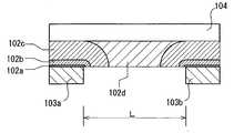
또한, 스퍼터링법에 의해, 층간 절연체(106)를 형성한다. 층간 절연체(106)는, 유전률이 낮은 재료를 이용하는 형성하는 것이 바람직하다. 본 실시 형태에서, 층간 절연체(106)는, CVD법에 의해 형성한 두께 300nm의 산화 실리콘막이다. 도 4c에 도시한 바와 같이, 층간 절연체(106)를 화학적 기계적 연마(CMP)법에 의해 평탄화한다.Further, the
그 후, 반도체층(102)에 도달하는 콘택트 홀을 형성하고, 제1 도체 전극(103a), 제2 도체 전극(103b) 및 제3 도체 전극(103c)을 형성한다. 본 실시 형태에서는, 제1 도체 전극(103a), 제2 도체 전극(103b) 및 제3 도체 전극(103c)은, 두께 50nm의 질화 티타늄막과 두께 150nm의 티타늄막을, 스퍼터링법에 의해 연속적으로 형성하고, 이것을 패터닝하여 형성한다. 이러한 방식으로, 도 4d에 도시되는 반도체 회로가 형성된다.Thereafter, a contact hole reaching the
반도체층(102)의, 게이트(105)가 형성된 도 4d의 좌측 부분은, FET의 활성층으로서 기능하고, 게이트(105)가 구비되지 않는 도 4d의 우측 부분은 저항으로서 기능한다. 이 회로는 도 6a에 도시한 인버터로서 이용할 수 있다.The left portion of FIG. 4D in which the
(제4 실시 형태)(Fourth Embodiment)
제1 내지 제3 실시 형태에서 설명한 반도체 장치는, 다양한 전자 기기, 예를 들어, 액정 디스플레이, EL(electro luminescent) 디스플레이, FE(field emission)디스플레이 등의 표시 장치용 구동 회로, 이미지 센서용 구동 회로, 반도체 메모리 등에 이용할 수 있다. 또한, 제1 내지 제3 실시 형태에서 설명한 반도체 장치는 상술한 전자 기기를 포함하는 전자 기기, 예를 들어, 텔레비전, 퍼스널 컴퓨터, 휴대 전화 등의 통신 기기, 전자 노트북, 휴대용 음악 플레이어 등에 이용될 수 있다.The semiconductor device described in the first to third embodiments can be applied to various electronic devices such as a driving circuit for a display device such as a liquid crystal display, an EL (electro luminescent) display, an FE (field emission) , Semiconductor memories, and the like. The semiconductor device described in the first to third embodiments can be used in an electronic device including the above-described electronic device, for example, a communication device such as a television, a personal computer, a mobile phone, an electronic notebook, have.
본 출원은 2010년 2월 5일 일본 특허청에 출원된 일본 특허 출원 제2010-024580호를 기초로 하고, 그 전체 내용은 본 명세서에서 참조로 원용된다.This application is based on Japanese Patent Application No. 2010-024580 filed on February 5, 2010, the Japanese Patent Office, the entire contents of which are incorporated herein by reference.
101 : 기판, 102 : 반도체층, 103a : 제1 도체 전극, 103b : 제2 도체 전극, 103c : 제3 도체 전극, 104 : 게이트 절연막, 105 : 게이트, 106 : 층간 절연체The present invention relates to a semiconductor device and a method of fabricating the same, and more particularly, to a semiconductor device comprising a substrate, a semiconductor layer, a first conductor electrode, a second conductor electrode,
Claims (42)
Translated fromKorean상기 전계 효과 트랜지스터는,
산화물 반도체를 포함하는 반도체층과,
상기 반도체층의 한쪽 면에 접하여 제공되는 제1 도체 전극 및 제2 도체 전극과,
상기 반도체층의 다른 쪽 면측에 제공되는 게이트를 포함하고,
상기 제1 도체 전극과 상기 게이트 사이의 영역, 및 상기 제2 도체 전극과 상기 게이트 사이의 영역 중 적어도 하나에 오프셋 영역이 제공되며,
상기 산화물 반도체의 캐리어 농도는 1012/cm3 이하이고,
상기 전계 효과 트랜지스터가 온(ON) 상태일 때의 저항을 RON, 상기 전계 효과 트랜지스터가 오프(OFF) 상태일 때의 저항을 ROFF라고 할 때, ROFF/RON이 1010 이상인, 반도체 장치.1. A semiconductor device comprising a field effect transistor,
Wherein the field effect transistor comprises:
A semiconductor layer including an oxide semiconductor;
A first conductor electrode and a second conductor electrode provided in contact with one surface of the semiconductor layer,
And a gate provided on the other surface side of the semiconductor layer,
An offset region is provided in at least one of a region between the first conductor electrode and the gate, and a region between the second conductor electrode and the gate,
The carrier concentration of the oxide semiconductor is 10 <12 > / cm <3 &
When the resistance of when the field effect transistor is turned on (ON) state, the resistance RON, the field effect transistor is turned off at the time (OFF) state to said ROFF, ROFF / RON is 1010 or more, a semiconductor Device.
상기 전계 효과 트랜지스터는,
산화물 반도체를 포함하는 반도체층과,
상기 반도체층의 한쪽 면에 접하여 제공되는 제1 도체 전극 및 제2 도체 전극과,
상기 반도체층의 상기 한쪽 면 위에 제공되는 게이트를 포함하고,
상기 제1 도체 전극과 상기 게이트 사이의 영역, 및 상기 제2 도체 전극과 상기 게이트 사이의 영역 중 적어도 하나에 오프셋 영역이 제공되며,
상기 산화물 반도체의 캐리어 농도는 1012/cm3 이하이고,
상기 전계 효과 트랜지스터가 온(ON) 상태일 때의 저항을 RON, 상기 전계 효과 트랜지스터가 오프(OFF) 상태일 때의 저항을 ROFF라고 할 때, ROFF/RON이 1010 이상인, 반도체 장치.1. A semiconductor device comprising a field effect transistor,
Wherein the field effect transistor comprises:
A semiconductor layer including an oxide semiconductor;
A first conductor electrode and a second conductor electrode provided in contact with one surface of the semiconductor layer,
And a gate provided on the one side of the semiconductor layer,
An offset region is provided in at least one of a region between the first conductor electrode and the gate, and a region between the second conductor electrode and the gate,
The carrier concentration of the oxide semiconductor is 10 <12 > / cm <3 &
When the resistance of when the field effect transistor is turned on (ON) state, the resistance RON, the field effect transistor is turned off at the time (OFF) state to said ROFF, ROFF / RON is 1010 or more, a semiconductor Device.
산화물 반도체를 포함하는 반도체층과,
상기 반도체층의 한쪽 면에 접하여 제공되는 제1 도체 전극, 제2 도체 전극 및 제3 도체 전극과,
상기 반도체층의 다른 쪽 면측에 제공되는 게이트를 포함하고,
상기 게이트는 상기 제1 도체 전극과 상기 제2 도체 전극 사이의 영역의 적어도 일부와 중첩되고,
상기 게이트는 상기 제2 도체 전극과 상기 제3 도체 전극 사이의 영역과 중첩되지 않으며,
상기 산화물 반도체의 캐리어 농도는 1012/cm3이하이고,
위에서 본 상기 제1 도체 전극과 상기 제2 도체 전극 사이의 상기 반도체층의 제1 부분의 폭은, 위에서 본 상기 제2 도체 전극과 상기 제3 도체 전극 사이의 상기 반도체층의 제2 부분의 폭보다 넓은, 반도체 장치.A semiconductor device comprising:
A semiconductor layer including an oxide semiconductor;
A first conductive electrode, a second conductive electrode, and a third conductive electrode provided in contact with one surface of the semiconductor layer;
And a gate provided on the other surface side of the semiconductor layer,
The gate overlaps at least a portion of the region between the first conductor electrode and the second conductor electrode,
The gate does not overlap a region between the second conductor electrode and the third conductor electrode,
The carrier concentration of the oxide semiconductor is 10 <12 > / cm <3 &
The width of the first portion of the semiconductor layer between the first conductor electrode and the second conductor electrode seen from above is equal to the width of the second portion of the semiconductor layer between the second conductor electrode viewed from above and the third conductor electrode . ≪ / RTI >
산화물 반도체를 포함하는 반도체층과,
상기 반도체층의 한쪽 면에 접하여 제공되는 제1 도체 전극, 제2 도체 전극 및 제3 도체 전극과,
상기 반도체층의 상기 한쪽 면 위에 제공되는 게이트를 포함하고,
상기 게이트는 상기 제1 도체 전극과 상기 제2 도체 전극 사이의 영역의 적어도 일부와 중첩되고,
상기 게이트는 상기 제2 도체 전극과 상기 제3 도체 전극 사이의 영역과 중첩되지 않으며,
상기 산화물 반도체의 캐리어 농도는 1012/cm3 이하이고,
위에서 본 상기 제1 도체 전극과 상기 제2 도체 전극 사이의 상기 반도체층의 제1 부분의 폭은, 위에서 본 상기 제2 도체 전극과 상기 제3 도체 전극 사이의 상기 반도체층의 제2 부분의 폭보다 넓은, 반도체 장치.A semiconductor device comprising:
A semiconductor layer including an oxide semiconductor;
A first conductive electrode, a second conductive electrode, and a third conductive electrode provided in contact with one surface of the semiconductor layer;
And a gate provided on the one side of the semiconductor layer,
The gate overlaps at least a portion of the region between the first conductor electrode and the second conductor electrode,
The gate does not overlap a region between the second conductor electrode and the third conductor electrode,
The carrier concentration of the oxide semiconductor is 10 <12 > / cm <3 &
The width of the first portion of the semiconductor layer between the first conductor electrode and the second conductor electrode seen from above is equal to the width of the second portion of the semiconductor layer between the second conductor electrode viewed from above and the third conductor electrode . ≪ / RTI >
산화물 반도체를 포함하는 반도체층과,
상기 반도체층의 한쪽 면에 접하여 제공되는 제1 도체 전극, 제2 도체 전극 및 제3 도체 전극과,
상기 반도체층의 다른 쪽 면측에 제공되는 게이트를 포함하고,
상기 게이트는 상기 제1 도체 전극과 상기 제2 도체 전극 사이의 영역의 적어도 일부와 중첩되고,
상기 게이트는 상기 제2 도체 전극과 상기 제3 도체 전극 사이의 영역과 중첩되지 않고,
상기 제1 도체 전극과 상기 게이트 사이의 영역, 및 상기 제2 도체 전극과 상기 게이트 사이의 영역 중 적어도 하나에 오프셋 영역이 제공되며,
상기 산화물 반도체의 캐리어 농도는 1012/cm3 이하이고,
상기 오프셋 영역의 폭은 10nm 이상 100nm 이하인, 반도체 장치.A semiconductor device comprising:
A semiconductor layer including an oxide semiconductor;
A first conductive electrode, a second conductive electrode, and a third conductive electrode provided in contact with one surface of the semiconductor layer;
And a gate provided on the other surface side of the semiconductor layer,
The gate overlaps at least a portion of the region between the first conductor electrode and the second conductor electrode,
The gate does not overlap a region between the second conductor electrode and the third conductor electrode,
An offset region is provided in at least one of a region between the first conductor electrode and the gate, and a region between the second conductor electrode and the gate,
The carrier concentration of the oxide semiconductor is 10 <12 > / cm <3 &
Wherein a width of the offset region is 10 nm or more and 100 nm or less.
산화물 반도체를 포함하는 반도체층과,
상기 반도체층의 한쪽 면에 접하여 제공되는 제1 도체 전극, 제2 도체 전극 및 제3 도체 전극과,
상기 반도체층의 상기 한쪽 면 위에 제공되는 게이트를 포함하고,
상기 게이트는 상기 제1 도체 전극과 상기 제2 도체 전극 사이의 영역의 적어도 일부와 중첩되고,
상기 게이트는 상기 제2 도체 전극과 상기 제3 도체 전극 사이의 영역과 중첩되지 않고,
상기 제1 도체 전극과 상기 게이트 사이의 영역, 및 상기 제2 도체 전극과 상기 게이트 사이의 영역 중 적어도 하나에 오프셋 영역이 제공되며,
상기 산화물 반도체의 캐리어 농도는 1012/cm3 이하이고,
상기 오프셋 영역의 폭은 10nm 이상 100nm 이하인, 반도체 장치.A semiconductor device comprising:
A semiconductor layer including an oxide semiconductor;
A first conductive electrode, a second conductive electrode, and a third conductive electrode provided in contact with one surface of the semiconductor layer;
And a gate provided on the one side of the semiconductor layer,
The gate overlaps at least a portion of the region between the first conductor electrode and the second conductor electrode,
The gate does not overlap a region between the second conductor electrode and the third conductor electrode,
An offset region is provided in at least one of a region between the first conductor electrode and the gate, and a region between the second conductor electrode and the gate,
The carrier concentration of the oxide semiconductor is 10 <12 > / cm <3 &
Wherein a width of the offset region is 10 nm or more and 100 nm or less.
상기 반도체층과 상기 게이트 사이에 게이트 절연막을 더 포함하는, 반도체 장치.7. The method according to any one of claims 1 to 6,
And a gate insulating film between the semiconductor layer and the gate.
상기 반도체층과 접하는 상기 제1 도체 전극의 부분과 상기 제2 도체 전극의 부분은, 상기 반도체층의 전자 친화력과 0.3 전자 볼트의 합보다 작은 일함수를 갖는, 반도체 장치.7. The method according to any one of claims 1 to 6,
Wherein a portion of the first conductive electrode in contact with the semiconductor layer and a portion of the second conductive electrode have a work function that is less than a sum of the electron affinity of the semiconductor layer and 0.3 electron volts.
상기 반도체층에 가장 근접한 상기 게이트의 부분의 일함수는, 상기 반도체층의 전자 친화력과 0.6 전자 볼트의 합보다 큰, 반도체 장치.7. The method according to any one of claims 1 to 6,
Wherein the work function of the portion of the gate closest to the semiconductor layer is greater than the sum of the electron affinity of the semiconductor layer and 0.6 electron volts.
상기 반도체층과 상기 제1 도체 전극 사이 및 상기 반도체층과 상기 제2 도체 전극 사이에는 오믹 접합이 형성되는, 반도체 장치.7. The method according to any one of claims 1 to 6,
And an ohmic contact is formed between the semiconductor layer and the first conductor electrode and between the semiconductor layer and the second conductor electrode.
상기 산화물 반도체는 i형 반도체인, 반도체 장치.7. The method according to any one of claims 1 to 6,
Wherein the oxide semiconductor is an i-type semiconductor.
상기 반도체층의 밴드 갭은 2 전자 볼트 이상 4 전자 볼트 미만인, 반도체 장치.7. The method according to any one of claims 1 to 6,
Wherein a band gap of the semiconductor layer is 2 electron volts or more and less than 4 electron volts.
상기 게이트는, 백금, 금, 텅스텐 및 질화 인듐으로 이루어진 그룹으로부터 선택된 재료를 포함하는, 반도체 장치.7. The method according to any one of claims 1 to 6,
Wherein the gate comprises a material selected from the group consisting of platinum, gold, tungsten, and indium nitride.
상기 오프셋 영역의 폭은 10nm 이상 100nm 이하인, 반도체 장치.3. The method according to claim 1 or 2,
Wherein a width of the offset region is 10 nm or more and 100 nm or less.
위에서 본 상기 제1 도체 전극과 상기 제2 도체 전극 사이의 상기 반도체층의 제1 부분의 폭은, 위에서 본 상기 제2 도체 전극과 상기 제3 도체 전극 사이의 상기 반도체층의 제2 부분의 폭보다 넓은, 반도체 장치.The method according to claim 5 or 6,
The width of the first portion of the semiconductor layer between the first conductor electrode and the second conductor electrode seen from above is equal to the width of the second portion of the semiconductor layer between the second conductor electrode viewed from above and the third conductor electrode . ≪ / RTI >
상기 반도체 장치는 인버터인, 반도체 장치.7. The method according to any one of claims 3 to 6,
Wherein the semiconductor device is an inverter.
상기 반도체 장치는 인버터이고,
상기 게이트에 입력 신호가 입력되면 상기 제2 도체 전극으로부터 출력 신호가 출력되는, 반도체 장치.7. The method according to any one of claims 3 to 6,
The semiconductor device is an inverter,
And an output signal is output from the second conductor electrode when an input signal is input to the gate.
상기 제2 도체 전극과 상기 제3 도체 전극 사이의 상기 반도체층은 저항으로서 기능하는, 반도체 장치.7. The method according to any one of claims 3 to 6,
And the semiconductor layer between the second conductor electrode and the third conductor electrode functions as a resistor.
Applications Claiming Priority (3)
| Application Number | Priority Date | Filing Date | Title |
|---|---|---|---|
| JP2010024580 | 2010-02-05 | ||
| JPJP-P-2010-024580 | 2010-02-05 | ||
| PCT/JP2011/051143WO2011096286A1 (en) | 2010-02-05 | 2011-01-17 | Field effect transistor and semiconductor device |
Publications (2)
| Publication Number | Publication Date |
|---|---|
| KR20120112647A KR20120112647A (en) | 2012-10-11 |
| KR101791713B1true KR101791713B1 (en) | 2017-10-30 |
Family
ID=44353022
Family Applications (1)
| Application Number | Title | Priority Date | Filing Date |
|---|---|---|---|
| KR1020127019627AExpired - Fee RelatedKR101791713B1 (en) | 2010-02-05 | 2011-01-17 | Field effect transistor and semiconductor device |
Country Status (5)
| Country | Link |
|---|---|
| US (2) | US8436431B2 (en) |
| JP (6) | JP5715432B2 (en) |
| KR (1) | KR101791713B1 (en) |
| TW (2) | TWI570919B (en) |
| WO (1) | WO2011096286A1 (en) |
Families Citing this family (19)
| Publication number | Priority date | Publication date | Assignee | Title |
|---|---|---|---|---|
| WO2011099342A1 (en)* | 2010-02-10 | 2011-08-18 | Semiconductor Energy Laboratory Co., Ltd. | Field effect transistor |
| US9209314B2 (en)* | 2010-06-16 | 2015-12-08 | Semiconductor Energy Laboratory Co., Ltd. | Field effect transistor |
| KR101856722B1 (en) | 2010-09-22 | 2018-05-10 | 가부시키가이샤 한도오따이 에네루기 켄큐쇼 | Power-insulated-gate field-effect transistor |
| US8736315B2 (en) | 2011-09-30 | 2014-05-27 | Semiconductor Energy Laboratory Co., Ltd. | Semiconductor device |
| WO2013065600A1 (en)* | 2011-11-02 | 2013-05-10 | シャープ株式会社 | Thin-film transistor, method for manufacturing same, and display device |
| JP6099372B2 (en) | 2011-12-05 | 2017-03-22 | 株式会社半導体エネルギー研究所 | Semiconductor device and electronic equipment |
| US9196741B2 (en)* | 2012-02-03 | 2015-11-24 | Semiconductor Energy Laboratory Co., Ltd. | Semiconductor device |
| JP6505769B2 (en)* | 2012-04-13 | 2019-04-24 | 株式会社半導体エネルギー研究所 | Semiconductor device |
| TWI662698B (en)* | 2012-11-28 | 2019-06-11 | 日商半導體能源研究所股份有限公司 | Display device |
| US9401432B2 (en) | 2014-01-16 | 2016-07-26 | Semiconductor Energy Laboratory Co., Ltd. | Semiconductor device and electronic device |
| JP6324528B2 (en)* | 2014-11-13 | 2018-05-16 | 三菱電機株式会社 | Manufacturing method of waterproof control unit |
| JP6693885B2 (en)* | 2014-11-20 | 2020-05-13 | 株式会社半導体エネルギー研究所 | Semiconductor device |
| JP6940508B2 (en)* | 2016-08-30 | 2021-09-29 | リンテック株式会社 | Resin compositions, resin sheets, and semiconductor devices |
| JP6648671B2 (en)* | 2016-11-15 | 2020-02-14 | 株式会社デンソー | Metal member, composite of metal member and resin member, and method of manufacturing the same |
| CN107623041B (en)* | 2017-09-08 | 2021-05-28 | 河南大学 | A kind of inverter based on oxide thin film transistor and its manufacturing method |
| FR3092633B1 (en) | 2019-02-08 | 2021-01-22 | Hutchinson | Vibration damping device, vessel fitted with such a device and related method. |
| US11404543B2 (en)* | 2020-06-19 | 2022-08-02 | Taiwan Semiconductor Manufacturing Company, Ltd. | Semiconductor device and manufacturing method thereof |
| JP7292466B2 (en)* | 2020-08-20 | 2023-06-16 | 株式会社半導体エネルギー研究所 | semiconductor equipment |
| WO2025141646A1 (en)* | 2023-12-25 | 2025-07-03 | 株式会社ニコン | Semiconductor device, electronic device, ph sensor, biosensor, and method for producing semiconductor device |
Citations (1)
| Publication number | Priority date | Publication date | Assignee | Title |
|---|---|---|---|---|
| JP2007103918A (en)* | 2005-09-06 | 2007-04-19 | Canon Inc | Field effect transistor using amorphous oxide film for channel layer, method for manufacturing field effect transistor using amorphous oxide film for channel layer, and method for manufacturing amorphous oxide film |
Family Cites Families (136)
| Publication number | Priority date | Publication date | Assignee | Title |
|---|---|---|---|---|
| JPS56115558A (en)* | 1980-02-18 | 1981-09-10 | Matsushita Electric Ind Co Ltd | Semiconductor integrated circuit and manufacture thereof |
| JPS58122774A (en)* | 1982-01-14 | 1983-07-21 | Toshiba Corp | Semiconductor device and manufacture thereof |
| JPH06104431A (en)* | 1992-09-11 | 1994-04-15 | Hitachi Ltd | Logic circuit, line image sensor using the same, and facsimile apparatus using the line image sensor |
| JP2887032B2 (en)* | 1992-10-30 | 1999-04-26 | シャープ株式会社 | Thin film transistor circuit and method of manufacturing the same |
| US5863823A (en) | 1993-07-12 | 1999-01-26 | Peregrine Semiconductor Corporation | Self-aligned edge control in silicon on insulator |
| US5416043A (en) | 1993-07-12 | 1995-05-16 | Peregrine Semiconductor Corporation | Minimum charge FET fabricated on an ultrathin silicon on sapphire wafer |
| US5930638A (en) | 1993-07-12 | 1999-07-27 | Peregrine Semiconductor Corp. | Method of making a low parasitic resistor on ultrathin silicon on insulator |
| US5864162A (en) | 1993-07-12 | 1999-01-26 | Peregrine Seimconductor Corporation | Apparatus and method of making a self-aligned integrated resistor load on ultrathin silicon on sapphire |
| US5572040A (en) | 1993-07-12 | 1996-11-05 | Peregrine Semiconductor Corporation | High-frequency wireless communication system on a single ultrathin silicon on sapphire chip |
| US5973363A (en) | 1993-07-12 | 1999-10-26 | Peregrine Semiconductor Corp. | CMOS circuitry with shortened P-channel length on ultrathin silicon on insulator |
| US5973382A (en) | 1993-07-12 | 1999-10-26 | Peregrine Semiconductor Corporation | Capacitor on ultrathin semiconductor on insulator |
| US5581092A (en) | 1993-09-07 | 1996-12-03 | Semiconductor Energy Laboratory Co., Ltd. | Gate insulated semiconductor device |
| JP3312083B2 (en) | 1994-06-13 | 2002-08-05 | 株式会社半導体エネルギー研究所 | Display device |
| TW345654B (en) | 1995-02-15 | 1998-11-21 | Handotai Energy Kenkyusho Kk | Active matrix display device |
| JPH11500268A (en)* | 1995-02-16 | 1999-01-06 | ペラグリン セミコンダクター コーポレイション | Resistive load for integrated circuit, method for producing the same, and SRAM |
| KR100394896B1 (en) | 1995-08-03 | 2003-11-28 | 코닌클리케 필립스 일렉트로닉스 엔.브이. | A semiconductor device including a transparent switching element |
| JP3625598B2 (en) | 1995-12-30 | 2005-03-02 | 三星電子株式会社 | Manufacturing method of liquid crystal display device |
| JPH09219493A (en)* | 1996-02-08 | 1997-08-19 | Hitachi Ltd | Resistance element, manufacturing method thereof, and semiconductor device in which the resistance element is integrated |
| JP3499381B2 (en) | 1996-09-21 | 2004-02-23 | 株式会社半導体エネルギー研究所 | Active matrix display device and manufacturing method thereof |
| JP4170454B2 (en) | 1998-07-24 | 2008-10-22 | Hoya株式会社 | Article having transparent conductive oxide thin film and method for producing the same |
| JP3293563B2 (en)* | 1998-08-13 | 2002-06-17 | 日本電気株式会社 | Field effect transistor and driving method thereof |
| JP2000150861A (en) | 1998-11-16 | 2000-05-30 | Tdk Corp | Oxide thin film |
| JP3276930B2 (en) | 1998-11-17 | 2002-04-22 | 科学技術振興事業団 | Transistor and semiconductor device |
| US6531713B1 (en) | 1999-03-19 | 2003-03-11 | Semiconductor Energy Laboratory Co., Ltd. | Electro-optical device and manufacturing method thereof |
| TW460731B (en) | 1999-09-03 | 2001-10-21 | Ind Tech Res Inst | Electrode structure and production method of wide viewing angle LCD |
| JP4089858B2 (en) | 2000-09-01 | 2008-05-28 | 国立大学法人東北大学 | Semiconductor device |
| KR20020038482A (en) | 2000-11-15 | 2002-05-23 | 모리시타 요이찌 | Thin film transistor array, method for producing the same, and display panel using the same |
| JP2003050405A (en)* | 2000-11-15 | 2003-02-21 | Matsushita Electric Ind Co Ltd | Thin film transistor array, method of manufacturing the same, and display panel using the same |
| JP3997731B2 (en) | 2001-03-19 | 2007-10-24 | 富士ゼロックス株式会社 | Method for forming a crystalline semiconductor thin film on a substrate |
| JP2002289859A (en) | 2001-03-23 | 2002-10-04 | Minolta Co Ltd | Thin film transistor |
| JP4090716B2 (en) | 2001-09-10 | 2008-05-28 | 雅司 川崎 | Thin film transistor and matrix display device |
| JP3925839B2 (en) | 2001-09-10 | 2007-06-06 | シャープ株式会社 | Semiconductor memory device and test method thereof |
| WO2003040441A1 (en) | 2001-11-05 | 2003-05-15 | Japan Science And Technology Agency | Natural superlattice homologous single crystal thin film, method for preparation thereof, and device using said single crystal thin film |
| JP4164562B2 (en) | 2002-09-11 | 2008-10-15 | 独立行政法人科学技術振興機構 | Transparent thin film field effect transistor using homologous thin film as active layer |
| JP4083486B2 (en) | 2002-02-21 | 2008-04-30 | 独立行政法人科学技術振興機構 | Method for producing LnCuO (S, Se, Te) single crystal thin film |
| CN1445821A (en) | 2002-03-15 | 2003-10-01 | 三洋电机株式会社 | Forming method of ZnO film and ZnO semiconductor layer, semiconductor element and manufacturing method thereof |
| JP3933591B2 (en) | 2002-03-26 | 2007-06-20 | 淳二 城戸 | Organic electroluminescent device |
| US7339187B2 (en) | 2002-05-21 | 2008-03-04 | State Of Oregon Acting By And Through The Oregon State Board Of Higher Education On Behalf Of Oregon State University | Transistor structures |
| JP2004022625A (en) | 2002-06-13 | 2004-01-22 | Murata Mfg Co Ltd | Semiconductor device and method of manufacturing the semiconductor device |
| US7105868B2 (en) | 2002-06-24 | 2006-09-12 | Cermet, Inc. | High-electron mobility transistor with zinc oxide |
| JP3818247B2 (en) | 2002-09-25 | 2006-09-06 | 凸版印刷株式会社 | Printed matter |
| US7067843B2 (en) | 2002-10-11 | 2006-06-27 | E. I. Du Pont De Nemours And Company | Transparent oxide semiconductor thin film transistors |
| JP2004193446A (en)* | 2002-12-13 | 2004-07-08 | Sanyo Electric Co Ltd | Method for manufacturing semiconductor device and method for manufacturing thin film transistor |
| JP4166105B2 (en) | 2003-03-06 | 2008-10-15 | シャープ株式会社 | Semiconductor device and manufacturing method thereof |
| JP2004273732A (en) | 2003-03-07 | 2004-09-30 | Sharp Corp | Active matrix substrate and manufacturing method thereof |
| US7129539B2 (en)* | 2003-05-15 | 2006-10-31 | Sharp Kabushiki Kaisha | Semiconductor storage device and manufacturing method therefor, semiconductor device, portable electronic equipment and IC card |
| JP4108633B2 (en) | 2003-06-20 | 2008-06-25 | シャープ株式会社 | THIN FILM TRANSISTOR, MANUFACTURING METHOD THEREOF, AND ELECTRONIC DEVICE |
| JP2005051223A (en)* | 2003-07-11 | 2005-02-24 | Nec Corp | Thin film transistor, tft substrate, liquid crystal display, and method for manufacturing tft |
| US7365361B2 (en) | 2003-07-23 | 2008-04-29 | Semiconductor Energy Laboratory Co., Ltd. | Semiconductor device and method for manufacturing the same |
| US7262463B2 (en) | 2003-07-25 | 2007-08-28 | Hewlett-Packard Development Company, L.P. | Transistor including a deposited channel region having a doped portion |
| JP2005079277A (en) | 2003-08-29 | 2005-03-24 | Toshiba Corp | Field effect transistor |
| US7145174B2 (en) | 2004-03-12 | 2006-12-05 | Hewlett-Packard Development Company, Lp. | Semiconductor device |
| US7282782B2 (en)* | 2004-03-12 | 2007-10-16 | Hewlett-Packard Development Company, L.P. | Combined binary oxide semiconductor device |
| US7297977B2 (en) | 2004-03-12 | 2007-11-20 | Hewlett-Packard Development Company, L.P. | Semiconductor device |
| CN1998087B (en)* | 2004-03-12 | 2014-12-31 | 独立行政法人科学技术振兴机构 | Amorphous oxide and thin film transistor |
| JP4245158B2 (en)* | 2004-04-19 | 2009-03-25 | パナソニック株式会社 | FET type ferroelectric memory cell and FET type ferroelectric memory |
| US7211825B2 (en) | 2004-06-14 | 2007-05-01 | Yi-Chi Shih | Indium oxide-based thin film transistors and circuits |
| JP2006100760A (en) | 2004-09-02 | 2006-04-13 | Casio Comput Co Ltd | Thin film transistor and manufacturing method thereof |
| US7285501B2 (en) | 2004-09-17 | 2007-10-23 | Hewlett-Packard Development Company, L.P. | Method of forming a solution processed device |
| US7298084B2 (en) | 2004-11-02 | 2007-11-20 | 3M Innovative Properties Company | Methods and displays utilizing integrated zinc oxide row and column drivers in conjunction with organic light emitting diodes |
| KR100953596B1 (en) | 2004-11-10 | 2010-04-21 | 캐논 가부시끼가이샤 | Light emitting device |
| JP5053537B2 (en) | 2004-11-10 | 2012-10-17 | キヤノン株式会社 | Semiconductor device using amorphous oxide |
| US7791072B2 (en) | 2004-11-10 | 2010-09-07 | Canon Kabushiki Kaisha | Display |
| AU2005302964B2 (en) | 2004-11-10 | 2010-11-04 | Canon Kabushiki Kaisha | Field effect transistor employing an amorphous oxide |
| US7829444B2 (en) | 2004-11-10 | 2010-11-09 | Canon Kabushiki Kaisha | Field effect transistor manufacturing method |
| EP2453481B1 (en) | 2004-11-10 | 2017-01-11 | Canon Kabushiki Kaisha | Field effect transistor with amorphous oxide |
| US7863611B2 (en) | 2004-11-10 | 2011-01-04 | Canon Kabushiki Kaisha | Integrated circuits utilizing amorphous oxides |
| US7453065B2 (en) | 2004-11-10 | 2008-11-18 | Canon Kabushiki Kaisha | Sensor and image pickup device |
| US7579224B2 (en) | 2005-01-21 | 2009-08-25 | Semiconductor Energy Laboratory Co., Ltd. | Method for manufacturing a thin film semiconductor device |
| TWI445178B (en) | 2005-01-28 | 2014-07-11 | Semiconductor Energy Lab | Semiconductor device, electronic device, and method of manufacturing semiconductor device |
| TWI505473B (en) | 2005-01-28 | 2015-10-21 | Semiconductor Energy Lab | Semiconductor device, electronic device, and method of manufacturing semiconductor device |
| US7858451B2 (en) | 2005-02-03 | 2010-12-28 | Semiconductor Energy Laboratory Co., Ltd. | Electronic device, semiconductor device and manufacturing method thereof |
| US7948171B2 (en) | 2005-02-18 | 2011-05-24 | Semiconductor Energy Laboratory Co., Ltd. | Light emitting device |
| US20060197092A1 (en) | 2005-03-03 | 2006-09-07 | Randy Hoffman | System and method for forming conductive material on a substrate |
| US8681077B2 (en) | 2005-03-18 | 2014-03-25 | Semiconductor Energy Laboratory Co., Ltd. | Semiconductor device, and display device, driving method and electronic apparatus thereof |
| US7544967B2 (en) | 2005-03-28 | 2009-06-09 | Massachusetts Institute Of Technology | Low voltage flexible organic/transparent transistor for selective gas sensing, photodetecting and CMOS device applications |
| US7645478B2 (en) | 2005-03-31 | 2010-01-12 | 3M Innovative Properties Company | Methods of making displays |
| US8300031B2 (en) | 2005-04-20 | 2012-10-30 | Semiconductor Energy Laboratory Co., Ltd. | Semiconductor device comprising transistor having gate and drain connected through a current-voltage conversion element |
| JP2006344849A (en) | 2005-06-10 | 2006-12-21 | Casio Comput Co Ltd | Thin film transistor |
| US7691666B2 (en) | 2005-06-16 | 2010-04-06 | Eastman Kodak Company | Methods of making thin film transistors comprising zinc-oxide-based semiconductor materials and transistors made thereby |
| US7402506B2 (en) | 2005-06-16 | 2008-07-22 | Eastman Kodak Company | Methods of making thin film transistors comprising zinc-oxide-based semiconductor materials and transistors made thereby |
| US7507618B2 (en) | 2005-06-27 | 2009-03-24 | 3M Innovative Properties Company | Method for making electronic devices using metal oxide nanoparticles |
| KR100711890B1 (en) | 2005-07-28 | 2007-04-25 | 삼성에스디아이 주식회사 | OLED display and manufacturing method thereof |
| JP2007059128A (en) | 2005-08-23 | 2007-03-08 | Canon Inc | Organic EL display device and manufacturing method thereof |
| JP2007073705A (en) | 2005-09-06 | 2007-03-22 | Canon Inc | Oxide semiconductor channel thin film transistor and method for manufacturing the same |
| JP4280736B2 (en) | 2005-09-06 | 2009-06-17 | キヤノン株式会社 | Semiconductor element |
| JP5116225B2 (en) | 2005-09-06 | 2013-01-09 | キヤノン株式会社 | Manufacturing method of oxide semiconductor device |
| JP4850457B2 (en) | 2005-09-06 | 2012-01-11 | キヤノン株式会社 | Thin film transistor and thin film diode |
| JP4981283B2 (en) | 2005-09-06 | 2012-07-18 | キヤノン株式会社 | Thin film transistor using amorphous oxide layer |
| EP1770788A3 (en) | 2005-09-29 | 2011-09-21 | Semiconductor Energy Laboratory Co., Ltd. | Semiconductor device having oxide semiconductor layer and manufacturing method thereof |
| JP5064747B2 (en)* | 2005-09-29 | 2012-10-31 | 株式会社半導体エネルギー研究所 | Semiconductor device, electrophoretic display device, display module, electronic device, and method for manufacturing semiconductor device |
| JP5037808B2 (en) | 2005-10-20 | 2012-10-03 | キヤノン株式会社 | Field effect transistor using amorphous oxide, and display device using the transistor |
| CN101577231B (en) | 2005-11-15 | 2013-01-02 | 株式会社半导体能源研究所 | Semiconductor device and method of manufacturing the same |
| JP2007142041A (en) | 2005-11-16 | 2007-06-07 | Toshiba Corp | Semiconductor device |
| TWI292281B (en) | 2005-12-29 | 2008-01-01 | Ind Tech Res Inst | Pixel structure of active organic light emitting diode and method of fabricating the same |
| US7867636B2 (en) | 2006-01-11 | 2011-01-11 | Murata Manufacturing Co., Ltd. | Transparent conductive film and method for manufacturing the same |
| JP4977478B2 (en) | 2006-01-21 | 2012-07-18 | 三星電子株式会社 | ZnO film and method of manufacturing TFT using the same |
| US7576394B2 (en) | 2006-02-02 | 2009-08-18 | Kochi Industrial Promotion Center | Thin film transistor including low resistance conductive thin films and manufacturing method thereof |
| US7977169B2 (en) | 2006-02-15 | 2011-07-12 | Kochi Industrial Promotion Center | Semiconductor device including active layer made of zinc oxide with controlled orientations and manufacturing method thereof |
| KR20070101595A (en) | 2006-04-11 | 2007-10-17 | 삼성전자주식회사 | ZnO TFT |
| US20070252928A1 (en) | 2006-04-28 | 2007-11-01 | Toppan Printing Co., Ltd. | Structure, transmission type liquid crystal display, reflection type display and manufacturing method thereof |
| JP5028033B2 (en) | 2006-06-13 | 2012-09-19 | キヤノン株式会社 | Oxide semiconductor film dry etching method |
| JP4609797B2 (en) | 2006-08-09 | 2011-01-12 | Nec液晶テクノロジー株式会社 | Thin film device and manufacturing method thereof |
| JP4999400B2 (en) | 2006-08-09 | 2012-08-15 | キヤノン株式会社 | Oxide semiconductor film dry etching method |
| JP4332545B2 (en) | 2006-09-15 | 2009-09-16 | キヤノン株式会社 | Field effect transistor and manufacturing method thereof |
| JP4274219B2 (en) | 2006-09-27 | 2009-06-03 | セイコーエプソン株式会社 | Electronic devices, organic electroluminescence devices, organic thin film semiconductor devices |
| JP5164357B2 (en) | 2006-09-27 | 2013-03-21 | キヤノン株式会社 | Semiconductor device and manufacturing method of semiconductor device |
| US7622371B2 (en) | 2006-10-10 | 2009-11-24 | Hewlett-Packard Development Company, L.P. | Fused nanocrystal thin film semiconductor and method |
| US7772021B2 (en) | 2006-11-29 | 2010-08-10 | Samsung Electronics Co., Ltd. | Flat panel displays comprising a thin-film transistor having a semiconductive oxide in its channel and methods of fabricating the same for use in flat panel displays |
| JP2008140684A (en) | 2006-12-04 | 2008-06-19 | Toppan Printing Co Ltd | Color EL display and manufacturing method thereof |
| KR101303578B1 (en) | 2007-01-05 | 2013-09-09 | 삼성전자주식회사 | Etching method of thin film |
| US8207063B2 (en) | 2007-01-26 | 2012-06-26 | Eastman Kodak Company | Process for atomic layer deposition |
| TWI478347B (en)* | 2007-02-09 | 2015-03-21 | Idemitsu Kosan Co | A thin film transistor, a thin film transistor substrate, and an image display device, and an image display device, and a semiconductor device |
| KR100851215B1 (en) | 2007-03-14 | 2008-08-07 | 삼성에스디아이 주식회사 | Thin film transistor and organic light emitting display device using same |
| US7795613B2 (en) | 2007-04-17 | 2010-09-14 | Toppan Printing Co., Ltd. | Structure with transistor |
| KR101325053B1 (en) | 2007-04-18 | 2013-11-05 | 삼성디스플레이 주식회사 | Thin film transistor substrate and manufacturing method thereof |
| KR20080094300A (en) | 2007-04-19 | 2008-10-23 | 삼성전자주식회사 | Thin film transistors and methods of manufacturing the same and flat panel displays comprising thin film transistors |
| KR101334181B1 (en) | 2007-04-20 | 2013-11-28 | 삼성전자주식회사 | Thin Film Transistor having selectively crystallized channel layer and method of manufacturing the same |
| CN101663762B (en) | 2007-04-25 | 2011-09-21 | 佳能株式会社 | Oxynitride semiconductor |
| KR101334182B1 (en)* | 2007-05-28 | 2013-11-28 | 삼성전자주식회사 | Fabrication method of ZnO family Thin film transistor |
| KR101345376B1 (en) | 2007-05-29 | 2013-12-24 | 삼성전자주식회사 | Fabrication method of ZnO family Thin film transistor |
| JP5242083B2 (en) | 2007-06-13 | 2013-07-24 | 出光興産株式会社 | Crystalline oxide semiconductor and thin film transistor using the same |
| JP5354999B2 (en) | 2007-09-26 | 2013-11-27 | キヤノン株式会社 | Method for manufacturing field effect transistor |
| JP5268132B2 (en)* | 2007-10-30 | 2013-08-21 | 富士フイルム株式会社 | Oxide semiconductor element and manufacturing method thereof, thin film sensor, and electro-optical device |
| CN101897031B (en)* | 2007-12-13 | 2013-04-17 | 出光兴产株式会社 | Field-effect transistor using oxide semiconductor and manufacturing method thereof |
| US8202365B2 (en) | 2007-12-17 | 2012-06-19 | Fujifilm Corporation | Process for producing oriented inorganic crystalline film, and semiconductor device using the oriented inorganic crystalline film |
| JP4555358B2 (en) | 2008-03-24 | 2010-09-29 | 富士フイルム株式会社 | Thin film field effect transistor and display device |
| JP5704790B2 (en)* | 2008-05-07 | 2015-04-22 | キヤノン株式会社 | Thin film transistor and display device |
| JP5202094B2 (en) | 2008-05-12 | 2013-06-05 | キヤノン株式会社 | Semiconductor device |
| KR100958006B1 (en)* | 2008-06-18 | 2010-05-17 | 삼성모바일디스플레이주식회사 | Thin film transistor, its manufacturing method, and flat panel display device comprising thin film transistor |
| JP5339792B2 (en)* | 2008-07-02 | 2013-11-13 | 富士フイルム株式会社 | Thin film field effect transistor, method of manufacturing the same, and display device using the same |
| JP2010021170A (en) | 2008-07-08 | 2010-01-28 | Hitachi Ltd | Semiconductor device, and method of manufacturing the same |
| JP5345349B2 (en)* | 2008-07-24 | 2013-11-20 | 富士フイルム株式会社 | Thin film field effect transistor |
| JP4623179B2 (en) | 2008-09-18 | 2011-02-02 | ソニー株式会社 | Thin film transistor and manufacturing method thereof |
| JP5451280B2 (en) | 2008-10-09 | 2014-03-26 | キヤノン株式会社 | Wurtzite crystal growth substrate, manufacturing method thereof, and semiconductor device |
| JP5629999B2 (en)* | 2009-09-29 | 2014-11-26 | 大日本印刷株式会社 | IC tag and manufacturing method thereof |
- 2011
- 2011-01-17KRKR1020127019627Apatent/KR101791713B1/ennot_activeExpired - Fee Related
- 2011-01-17WOPCT/JP2011/051143patent/WO2011096286A1/enactiveApplication Filing
- 2011-01-25TWTW100102652Apatent/TWI570919B/ennot_activeIP Right Cessation
- 2011-01-25TWTW105100941Apatent/TWI573276B/ennot_activeIP Right Cessation
- 2011-01-26USUS13/014,060patent/US8436431B2/enactiveActive
- 2011-02-04JPJP2011022507Apatent/JP5715432B2/ennot_activeExpired - Fee Related
- 2012
- 2012-08-21JPJP2012182291Apatent/JP2013008988A/ennot_activeWithdrawn
- 2013
- 2013-04-02USUS13/855,203patent/US8791529B2/enactiveActive
- 2013-04-19JPJP2013088009Apatent/JP5675886B2/ennot_activeExpired - Fee Related
- 2014
- 2014-12-11JPJP2014250947Apatent/JP5702886B1/ennot_activeExpired - Fee Related
- 2015
- 2015-03-13JPJP2015050708Apatent/JP6031547B2/ennot_activeExpired - Fee Related
- 2015-03-19JPJP2015056324Apatent/JP6096233B2/ennot_activeExpired - Fee Related
Patent Citations (1)
| Publication number | Priority date | Publication date | Assignee | Title |
|---|---|---|---|---|
| JP2007103918A (en)* | 2005-09-06 | 2007-04-19 | Canon Inc | Field effect transistor using amorphous oxide film for channel layer, method for manufacturing field effect transistor using amorphous oxide film for channel layer, and method for manufacturing amorphous oxide film |
Also Published As
| Publication number | Publication date |
|---|---|
| JP2013191856A (en) | 2013-09-26 |
| US8791529B2 (en) | 2014-07-29 |
| JP2015133513A (en) | 2015-07-23 |
| TWI573276B (en) | 2017-03-01 |
| TWI570919B (en) | 2017-02-11 |
| TW201614848A (en) | 2016-04-16 |
| JP2011181918A (en) | 2011-09-15 |
| JP2013008988A (en) | 2013-01-10 |
| JP5715432B2 (en) | 2015-05-07 |
| JP5702886B1 (en) | 2015-04-15 |
| JP2015073127A (en) | 2015-04-16 |
| US8436431B2 (en) | 2013-05-07 |
| JP5675886B2 (en) | 2015-02-25 |
| JP2015111742A (en) | 2015-06-18 |
| KR20120112647A (en) | 2012-10-11 |
| JP6096233B2 (en) | 2017-03-15 |
| US20110193182A1 (en) | 2011-08-11 |
| JP6031547B2 (en) | 2016-11-24 |
| WO2011096286A1 (en) | 2011-08-11 |
| US20130228776A1 (en) | 2013-09-05 |
| TW201143095A (en) | 2011-12-01 |
Similar Documents
| Publication | Publication Date | Title |
|---|---|---|
| KR101791713B1 (en) | Field effect transistor and semiconductor device | |
| US8492853B2 (en) | Field effect transistor having conductor electrode in contact with semiconductor layer | |
| US9911866B2 (en) | Field effect transistor | |
| JP6395845B2 (en) | Junction field effect transistor and complementary circuit incorporating junction field effect transistor | |
| US20110220878A1 (en) | Thin film transistor and method of manufacturing the same | |
| KR101856722B1 (en) | Power-insulated-gate field-effect transistor | |
| US7525136B2 (en) | JFET device with virtual source and drain link regions and method of fabrication | |
| US20130214854A1 (en) | Semiconductor device and method of driving the same | |
| US6781168B1 (en) | Semiconductor device | |
| EP4369414A2 (en) | Transistor with integrated short circuit protection | |
| JP2007173741A (en) | P-type thin film transistor, N-type thin film transistor, and semiconductor device | |
| JPS6167965A (en) | field effect semiconductor device |
Legal Events
| Date | Code | Title | Description |
|---|---|---|---|
| PA0105 | International application | St.27 status event code:A-0-1-A10-A15-nap-PA0105 | |
| PG1501 | Laying open of application | St.27 status event code:A-1-1-Q10-Q12-nap-PG1501 | |
| A201 | Request for examination | ||
| E13-X000 | Pre-grant limitation requested | St.27 status event code:A-2-3-E10-E13-lim-X000 | |
| P11-X000 | Amendment of application requested | St.27 status event code:A-2-2-P10-P11-nap-X000 | |
| P13-X000 | Application amended | St.27 status event code:A-2-2-P10-P13-nap-X000 | |
| PA0201 | Request for examination | St.27 status event code:A-1-2-D10-D11-exm-PA0201 | |
| E902 | Notification of reason for refusal | ||
| PE0902 | Notice of grounds for rejection | St.27 status event code:A-1-2-D10-D21-exm-PE0902 | |
| P11-X000 | Amendment of application requested | St.27 status event code:A-2-2-P10-P11-nap-X000 | |
| P13-X000 | Application amended | St.27 status event code:A-2-2-P10-P13-nap-X000 | |
| E701 | Decision to grant or registration of patent right | ||
| PE0701 | Decision of registration | St.27 status event code:A-1-2-D10-D22-exm-PE0701 | |
| GRNT | Written decision to grant | ||
| PR0701 | Registration of establishment | St.27 status event code:A-2-4-F10-F11-exm-PR0701 | |
| PR1002 | Payment of registration fee | St.27 status event code:A-2-2-U10-U12-oth-PR1002 Fee payment year number:1 | |
| PG1601 | Publication of registration | St.27 status event code:A-4-4-Q10-Q13-nap-PG1601 | |
| PC1903 | Unpaid annual fee | St.27 status event code:A-4-4-U10-U13-oth-PC1903 Not in force date:20201025 Payment event data comment text:Termination Category : DEFAULT_OF_REGISTRATION_FEE | |
| PC1903 | Unpaid annual fee | St.27 status event code:N-4-6-H10-H13-oth-PC1903 Ip right cessation event data comment text:Termination Category : DEFAULT_OF_REGISTRATION_FEE Not in force date:20201025 | |
| P22-X000 | Classification modified | St.27 status event code:A-4-4-P10-P22-nap-X000 |