KR101790365B1 - Semiconductor device - Google Patents
Semiconductor deviceDownload PDFInfo
- Publication number
- KR101790365B1 KR101790365B1KR1020127014553AKR20127014553AKR101790365B1KR 101790365 B1KR101790365 B1KR 101790365B1KR 1020127014553 AKR1020127014553 AKR 1020127014553AKR 20127014553 AKR20127014553 AKR 20127014553AKR 101790365 B1KR101790365 B1KR 101790365B1
- Authority
- KR
- South Korea
- Prior art keywords
- electrode
- transistor
- source
- oxide semiconductor
- drain electrode
- Prior art date
- Legal status (The legal status is an assumption and is not a legal conclusion. Google has not performed a legal analysis and makes no representation as to the accuracy of the status listed.)
- Expired - Fee Related
Links
Images


Classifications
- H—ELECTRICITY
- H10—SEMICONDUCTOR DEVICES; ELECTRIC SOLID-STATE DEVICES NOT OTHERWISE PROVIDED FOR
- H10B—ELECTRONIC MEMORY DEVICES
- H10B41/00—Electrically erasable-and-programmable ROM [EEPROM] devices comprising floating gates
- H10B41/70—Electrically erasable-and-programmable ROM [EEPROM] devices comprising floating gates the floating gate being an electrode shared by two or more components
- G—PHYSICS
- G11—INFORMATION STORAGE
- G11C—STATIC STORES
- G11C11/00—Digital stores characterised by the use of particular electric or magnetic storage elements; Storage elements therefor
- G11C11/21—Digital stores characterised by the use of particular electric or magnetic storage elements; Storage elements therefor using electric elements
- G11C11/34—Digital stores characterised by the use of particular electric or magnetic storage elements; Storage elements therefor using electric elements using semiconductor devices
- G11C11/40—Digital stores characterised by the use of particular electric or magnetic storage elements; Storage elements therefor using electric elements using semiconductor devices using transistors
- G11C11/401—Digital stores characterised by the use of particular electric or magnetic storage elements; Storage elements therefor using electric elements using semiconductor devices using transistors forming cells needing refreshing or charge regeneration, i.e. dynamic cells
- G11C11/403—Digital stores characterised by the use of particular electric or magnetic storage elements; Storage elements therefor using electric elements using semiconductor devices using transistors forming cells needing refreshing or charge regeneration, i.e. dynamic cells with charge regeneration common to a multiplicity of memory cells, i.e. external refresh
- H—ELECTRICITY
- H10—SEMICONDUCTOR DEVICES; ELECTRIC SOLID-STATE DEVICES NOT OTHERWISE PROVIDED FOR
- H10D—INORGANIC ELECTRIC SEMICONDUCTOR DEVICES
- H10D84/00—Integrated devices formed in or on semiconductor substrates that comprise only semiconducting layers, e.g. on Si wafers or on GaAs-on-Si wafers
- H10D84/01—Manufacture or treatment
- H10D84/02—Manufacture or treatment characterised by using material-based technologies
- H10D84/03—Manufacture or treatment characterised by using material-based technologies using Group IV technology, e.g. silicon technology or silicon-carbide [SiC] technology
- H10D84/038—Manufacture or treatment characterised by using material-based technologies using Group IV technology, e.g. silicon technology or silicon-carbide [SiC] technology using silicon technology, e.g. SiGe
- H—ELECTRICITY
- H10—SEMICONDUCTOR DEVICES; ELECTRIC SOLID-STATE DEVICES NOT OTHERWISE PROVIDED FOR
- H10D—INORGANIC ELECTRIC SEMICONDUCTOR DEVICES
- H10D84/00—Integrated devices formed in or on semiconductor substrates that comprise only semiconducting layers, e.g. on Si wafers or on GaAs-on-Si wafers
- H10D84/80—Integrated devices formed in or on semiconductor substrates that comprise only semiconducting layers, e.g. on Si wafers or on GaAs-on-Si wafers characterised by the integration of at least one component covered by groups H10D12/00 or H10D30/00, e.g. integration of IGFETs
- H—ELECTRICITY
- H10—SEMICONDUCTOR DEVICES; ELECTRIC SOLID-STATE DEVICES NOT OTHERWISE PROVIDED FOR
- H10D—INORGANIC ELECTRIC SEMICONDUCTOR DEVICES
- H10D86/00—Integrated devices formed in or on insulating or conducting substrates, e.g. formed in silicon-on-insulator [SOI] substrates or on stainless steel or glass substrates
- H10D86/201—Integrated devices formed in or on insulating or conducting substrates, e.g. formed in silicon-on-insulator [SOI] substrates or on stainless steel or glass substrates the substrates comprising an insulating layer on a semiconductor body, e.g. SOI
- H—ELECTRICITY
- H10—SEMICONDUCTOR DEVICES; ELECTRIC SOLID-STATE DEVICES NOT OTHERWISE PROVIDED FOR
- H10D—INORGANIC ELECTRIC SEMICONDUCTOR DEVICES
- H10D86/00—Integrated devices formed in or on insulating or conducting substrates, e.g. formed in silicon-on-insulator [SOI] substrates or on stainless steel or glass substrates
- H10D86/40—Integrated devices formed in or on insulating or conducting substrates, e.g. formed in silicon-on-insulator [SOI] substrates or on stainless steel or glass substrates characterised by multiple TFTs
- H10D86/421—Integrated devices formed in or on insulating or conducting substrates, e.g. formed in silicon-on-insulator [SOI] substrates or on stainless steel or glass substrates characterised by multiple TFTs having a particular composition, shape or crystalline structure of the active layer
- H10D86/423—Integrated devices formed in or on insulating or conducting substrates, e.g. formed in silicon-on-insulator [SOI] substrates or on stainless steel or glass substrates characterised by multiple TFTs having a particular composition, shape or crystalline structure of the active layer comprising semiconductor materials not belonging to the Group IV, e.g. InGaZnO
- H—ELECTRICITY
- H10—SEMICONDUCTOR DEVICES; ELECTRIC SOLID-STATE DEVICES NOT OTHERWISE PROVIDED FOR
- H10D—INORGANIC ELECTRIC SEMICONDUCTOR DEVICES
- H10D86/00—Integrated devices formed in or on insulating or conducting substrates, e.g. formed in silicon-on-insulator [SOI] substrates or on stainless steel or glass substrates
- H10D86/40—Integrated devices formed in or on insulating or conducting substrates, e.g. formed in silicon-on-insulator [SOI] substrates or on stainless steel or glass substrates characterised by multiple TFTs
- H10D86/60—Integrated devices formed in or on insulating or conducting substrates, e.g. formed in silicon-on-insulator [SOI] substrates or on stainless steel or glass substrates characterised by multiple TFTs wherein the TFTs are in active matrices
- H—ELECTRICITY
- H10—SEMICONDUCTOR DEVICES; ELECTRIC SOLID-STATE DEVICES NOT OTHERWISE PROVIDED FOR
- H10D—INORGANIC ELECTRIC SEMICONDUCTOR DEVICES
- H10D88/00—Three-dimensional [3D] integrated devices
- H—ELECTRICITY
- H10—SEMICONDUCTOR DEVICES; ELECTRIC SOLID-STATE DEVICES NOT OTHERWISE PROVIDED FOR
- H10D—INORGANIC ELECTRIC SEMICONDUCTOR DEVICES
- H10D88/00—Three-dimensional [3D] integrated devices
- H10D88/01—Manufacture or treatment
- H—ELECTRICITY
- H10—SEMICONDUCTOR DEVICES; ELECTRIC SOLID-STATE DEVICES NOT OTHERWISE PROVIDED FOR
- H10D—INORGANIC ELECTRIC SEMICONDUCTOR DEVICES
- H10D89/00—Aspects of integrated devices not covered by groups H10D84/00 - H10D88/00
- H10D89/10—Integrated device layouts
- G—PHYSICS
- G11—INFORMATION STORAGE
- G11C—STATIC STORES
- G11C11/00—Digital stores characterised by the use of particular electric or magnetic storage elements; Storage elements therefor
- G11C11/21—Digital stores characterised by the use of particular electric or magnetic storage elements; Storage elements therefor using electric elements
- G11C11/34—Digital stores characterised by the use of particular electric or magnetic storage elements; Storage elements therefor using electric elements using semiconductor devices
- G11C11/40—Digital stores characterised by the use of particular electric or magnetic storage elements; Storage elements therefor using electric elements using semiconductor devices using transistors
- G11C11/401—Digital stores characterised by the use of particular electric or magnetic storage elements; Storage elements therefor using electric elements using semiconductor devices using transistors forming cells needing refreshing or charge regeneration, i.e. dynamic cells
- G11C11/403—Digital stores characterised by the use of particular electric or magnetic storage elements; Storage elements therefor using electric elements using semiconductor devices using transistors forming cells needing refreshing or charge regeneration, i.e. dynamic cells with charge regeneration common to a multiplicity of memory cells, i.e. external refresh
- G11C11/405—Digital stores characterised by the use of particular electric or magnetic storage elements; Storage elements therefor using electric elements using semiconductor devices using transistors forming cells needing refreshing or charge regeneration, i.e. dynamic cells with charge regeneration common to a multiplicity of memory cells, i.e. external refresh with three charge-transfer gates, e.g. MOS transistors, per cell
- H—ELECTRICITY
- H01—ELECTRIC ELEMENTS
- H01L—SEMICONDUCTOR DEVICES NOT COVERED BY CLASS H10
- H01L21/00—Processes or apparatus adapted for the manufacture or treatment of semiconductor or solid state devices or of parts thereof
- H01L21/02—Manufacture or treatment of semiconductor devices or of parts thereof
- H01L21/02104—Forming layers
- H01L21/02365—Forming inorganic semiconducting materials on a substrate
- H01L21/02518—Deposited layers
- H01L21/02521—Materials
- H01L21/02551—Group 12/16 materials
- H01L21/02554—Oxides
- H—ELECTRICITY
- H01—ELECTRIC ELEMENTS
- H01L—SEMICONDUCTOR DEVICES NOT COVERED BY CLASS H10
- H01L21/00—Processes or apparatus adapted for the manufacture or treatment of semiconductor or solid state devices or of parts thereof
- H01L21/02—Manufacture or treatment of semiconductor devices or of parts thereof
- H01L21/02104—Forming layers
- H01L21/02365—Forming inorganic semiconducting materials on a substrate
- H01L21/02518—Deposited layers
- H01L21/02521—Materials
- H01L21/02565—Oxide semiconducting materials not being Group 12/16 materials, e.g. ternary compounds
- H—ELECTRICITY
- H01—ELECTRIC ELEMENTS
- H01L—SEMICONDUCTOR DEVICES NOT COVERED BY CLASS H10
- H01L21/00—Processes or apparatus adapted for the manufacture or treatment of semiconductor or solid state devices or of parts thereof
- H01L21/02—Manufacture or treatment of semiconductor devices or of parts thereof
- H01L21/02104—Forming layers
- H01L21/02365—Forming inorganic semiconducting materials on a substrate
- H01L21/02612—Formation types
- H01L21/02617—Deposition types
- H01L21/02631—Physical deposition at reduced pressure, e.g. MBE, sputtering, evaporation
Landscapes
- Engineering & Computer Science (AREA)
- Microelectronics & Electronic Packaging (AREA)
- Computer Hardware Design (AREA)
- Manufacturing & Machinery (AREA)
- Condensed Matter Physics & Semiconductors (AREA)
- General Physics & Mathematics (AREA)
- Physics & Mathematics (AREA)
- Power Engineering (AREA)
- Thin Film Transistor (AREA)
- Semiconductor Memories (AREA)
- Physical Vapour Deposition (AREA)
- Non-Volatile Memory (AREA)
- Dram (AREA)
- Electroluminescent Light Sources (AREA)
Abstract
Translated fromKoreanDescription
Translated fromKorean여기서 개시된 발명은 반도체 소자를 사용하는 반도체 장치 및 반도체 장치를 제조하기 위한 방법에 관한 것이다.The invention disclosed herein relates to a semiconductor device using a semiconductor element and a method for manufacturing the semiconductor device.
반도체 소자들을 사용하는 저장 장치들은 2개의 카테고리로 크게 분류된다: 전력 공급이 중단될 때 저장된 데이터를 유실하는 휘발성 저장 장치, 및 전력이 공급되지 않는 경우라도 저장된 데이터를 보유하는 비휘발성 저장 장치.Storage devices using semiconductor devices are broadly categorized into two categories: volatile storage devices that lose stored data when power is interrupted, and non-volatile storage devices that retain stored data even when power is not supplied.
휘발성 저장 장치의 통상적인 예는 DRAM(동적 랜덤 액세스 메모리)이다. DRAM은 저장 소자에 포함된 트랜지스터가 선택되고 전하가 용량 소자에 저장되는 방식으로 데이터를 저장한다.A typical example of a volatile storage device is DRAM (Dynamic Random Access Memory). The DRAM stores data in such a way that the transistors included in the storage element are selected and the charge is stored in the capacitive element.
전술된 원리들로 인해, 용량 소자 내의 전하는 데이터가 DRAM에서 판독되는 경우 유실된다; 따라서, 데이터를 판독한 이후 데이터가 다시 저장되도록 다시 기입을 수행하는 것이 필요하다. 또한, 저장 소자에 포함된 트랜지스터가 리크 전류를 갖고, 트랜지스터가 선택되지 않을 경우라도 전하가 용량 소자 내로 또는 용량 소자 밖으로 흐르며, 따라서, 데이터 유지 시간이 짧다. 이러한 이유로, 다른 기입 동작(리프레시 동작)이 미리 결정된 간격으로 필요하며, 전력 소모를 충분히 감소시키는 것이 어렵다. 또한, 전력 공급이 중단되는 경우 저장된 데이터가 유실되므로, 자기 재료 또는 광학 재료를 사용하는 추가적인 저장 장치가 긴 시간 동안 데이터를 유지하기 위해 요구된다.Due to the above-described principles, charge in the capacitive element is lost when data is read from the DRAM; Therefore, it is necessary to perform the rewriting so that the data is stored again after reading the data. Further, even if the transistor included in the storage element has a leak current and the transistor is not selected, the charge flows into the capacitor element or out of the capacitor element, and therefore, the data holding time is short. For this reason, another write operation (refresh operation) is required at predetermined intervals, and it is difficult to sufficiently reduce power consumption. Also, since stored data is lost when the power supply is interrupted, additional storage devices using magnetic materials or optical materials are required to hold data for a long time.
휘발성 저장 장치의 다른 예는 SRAM(정적 랜덤 액세스 메모리)이다. SRAM은 플립-플롭과 같은 회로를 사용함으로써 저장된 데이터를 유지하며 따라서 리프레시 동작을 요구하지 않는다. 이는 SRAM이 DRAM에 비해 장점을 가진다는 것을 의미한다. 그러나, 플립-플롭과 같은 회로가 사용되므로 저장 공간당 비용이 증가한다. 또한, DRAM에서와 같이, SRAM 내에 저장된 데이터는 전력 공급이 중단되는 경우 유실된다.Another example of a volatile storage device is SRAM (static random access memory). The SRAM maintains the stored data by using a circuit such as a flip-flop and thus does not require a refresh operation. This means that SRAM has advantages over DRAM. However, since a circuit such as a flip-flop is used, the cost per storage space increases. Also, as in DRAM, data stored in SRAM is lost when power supply is interrupted.
비휘발성 저장 장치의 통상적인 예는 플래시 메모리이다. 플래시 메모리는 트랜지스터 내의 채널 형성 영역과 게이트 전극 사이의 플로팅 게이트를 포함하며, 플로팅 게이트 내에 전하를 유지함으로써 데이터를 저장한다. 따라서, 플래시 메모리는 데이터 유지 시간이 극도로 길어지며(거의 영구적) 휘발성 저장 장치 내에서 필요한 리프레시 동작이 요구되지 않는다는 점에 있어서 장점들을 가진다(예를 들어, 특허 문헌 1을 참조)A typical example of a non-volatile storage device is flash memory. The flash memory includes a floating gate between the channel forming region and the gate electrode in the transistor, and stores data by holding charge in the floating gate. Therefore, the flash memory has advantages in that the data retention time becomes extremely long (almost permanent) and the necessary refresh operation is not required in the volatile storage device (see, for example, Patent Document 1)
그러나, 저장 소자 내에 포함된 게이트 절연층은 기입시 생성되는 전류를 터널링함으로써 악화되며, 따라서, 저장 소자는 미리 결정된 개수의 기입 동작들 이후 자신의 기능을 중지시킨다. 이러한 문제점의 악영향을 감소시키기 위해, 예를 들어, 저장 소자들에 대한 상기 개수의 기입 동작들이 등화되는 방법이 사용된다. 그러나, 이러한 방법을 구현하기 위해서는 복잡한 주변 회로가 요구된다. 또한, 이러한 방법을 사용하는 것은 기본적인 수명 문제를 해결하지 않는다. 다시 말해, 플래시 메모리는 데이터가 빈번하게 재기입되는 애플리케이션들에 대해 적절하지 않다.However, the gate insulating layer included in the storage element deteriorates by tunneling the current generated at the time of writing, and therefore, the storage element stops its function after a predetermined number of write operations. To reduce the adverse effects of this problem, for example, a method is used in which the number of write operations for storage elements is equalized. However, complicated peripheral circuits are required to implement such a method. Also, using this method does not solve the basic lifetime problem. In other words, flash memory is not appropriate for applications where data is frequently rewritten.
추가로, 플로팅 게이트에서 전하를 유지하거나 전하를 제거하기 위해 높은 전압이 필요하다. 또한, 전하를 유지하거나 제거하는데 상대적으로 긴 시간이 소요되며, 더욱 빠른 속도로 기입 및 소거를 수행하는 것이 용이하지 않다.In addition, a high voltage is needed to maintain charge or remove charge in the floating gate. Also, it takes a relatively long time to maintain or remove the charge, and it is not easy to perform writing and erasing at a higher speed.
전술된 문제점들의 견지에서, 여기서 개시된 발명의 일 실시 형태의 목적은 전력이 공급되지 않고 기입의 횟수가 제한되는 경우라도 저장된 데이터가 보유될 수 있는 신규한 구조를 반도체 장치에 제공하는 것이다.In view of the foregoing problems, an object of an embodiment of the invention disclosed herein is to provide a novel structure to a semiconductor device in which stored data can be retained even when power is not supplied and the number of writes is limited.
본 발명의 일 실시 형태는 산화물 반도체를 사용하여 형성되는 트랜지스터 및 산화물 반도체가 아닌 재료를 사용하여 형성되는 트랜지스터의 적층 구조를 갖는 반도체 장치이다. 예를 들어, 후속하는 구조들이 사용될 수 있다.One embodiment of the present invention is a semiconductor device having a stacked structure of transistors formed by using a material which is not an oxide semiconductor and an oxide semiconductor. For example, the following structures may be used.
본 발명의 실시 형태는 소스 라인, 비트 라인, 신호 라인, 및 워드 라인을 포함하는 반도체 장치이다. 복수의 메모리 셀은 소스 라인과 비트 라인 사이에 병렬로 접속되고, 복수의 메모리 셀 중 하나는 제1 게이트 전극, 제1 소스 전극 및 제1 드레인 전극을 포함하는 제1 트랜지스터, 제2 게이트 전극, 제2 소스 전극, 및 제2 드레인 전극을 포함하는 제2 트랜지스터, 및 용량 소자를 포함한다. 제1 트랜지스터는 반도체 재료를 포함하는 기판에 제공되고, 제2 트랜지스터는 산화물 반도체층을 포함한다. 제1 게이트 전극, 제2 소스 전극 및 제2 드레인 전극 중 하나, 및 용량 소자의 하나의 전극은 서로 전기적으로 접속된다. 소스 라인, 및 제1 소스 전극 및 제1 드레인 전극 중 하나는 서로 전기적으로 접속된다. 비트 라인 및 제1 소스 전극 및 제1 드레인 전극 중 다른 하나는 서로 전기적으로 접속된다. 신호 라인 및 제2 게이트 전극은 서로 전기적으로 접속된다. 워드 라인, 제2 소스 전극 및 제2 드레인 전극 중 다른 하나, 및 용량 소자의 다른 전극은 서로 전기적으로 접속된다.An embodiment of the present invention is a semiconductor device including a source line, a bit line, a signal line, and a word line. A plurality of memory cells are connected in parallel between a source line and a bit line, and one of the plurality of memory cells includes a first transistor including a first gate electrode, a first source electrode, and a first drain electrode, a second gate electrode, A second source electrode, and a second drain electrode, and a capacitive element. The first transistor is provided on a substrate including a semiconductor material, and the second transistor includes an oxide semiconductor layer. One of the first gate electrode, the second source electrode, and the second drain electrode, and one electrode of the capacitor element are electrically connected to each other. Source line, and one of the first source electrode and the first drain electrode are electrically connected to each other. The bit line and the other of the first source electrode and the first drain electrode are electrically connected to each other. The signal line and the second gate electrode are electrically connected to each other. The other of the word line, the second source electrode, and the second drain electrode, and the other electrode of the capacitor element are electrically connected to each other.
본 발명의 다른 실시 형태는 소스 라인, 비트 라인, 신호 라인, 및 워드 라인을 포함하는 반도체 장치이다. 복수의 메모리 셀은 소스 라인 및 비트 라인 사이에 병렬로 접속되고, 복수의 메모리 셀 중 하나는 제1 게이트 전극, 제1 소스 전극 및 제1 드레인 전극을 포함하는 제1 트랜지스터, 제2 게이트 전극, 제2 소스 전극 및 제2 드레인 전극을 포함하는 제2 트랜지스터, 및 용량 소자를 포함한다. 제1 트랜지스터는 반도체 재료를 포함하는 기판에 제공되고, 제2 트랜지스터는 산화물 반도체층을 포함한다. 제1 게이트 전극, 제2 소스 전극 및 제2 드레인 전극 중 하나, 및 용량 소자의 전극은 서로 전기적으로 접속된다. 소스 라인, 및 제1 소스 전극 및 제1 드레인 전극 중 하나는 서로 전기적으로 접속된다. 비트 라인, 및 제1 소스 전극 및 제1 드레인 전극 중 다른 하나는 서로 전기적으로 접속된다. 신호 라인, 및 제2 소스 전극 및 제2 드레인 전극 중 다른 하나는 서로 전기적으로 접속된다. 워드 라인, 제2 게이트 전극, 및 용량 소자의 다른 전극은 서로 전기적으로 접속된다.Another embodiment of the present invention is a semiconductor device including a source line, a bit line, a signal line, and a word line. A plurality of memory cells are connected in parallel between a source line and a bit line, and one of the plurality of memory cells includes a first transistor including a first gate electrode, a first source electrode, and a first drain electrode, a second gate electrode, A second transistor including a second source electrode and a second drain electrode, and a capacitive element. The first transistor is provided on a substrate including a semiconductor material, and the second transistor includes an oxide semiconductor layer. One of the first gate electrode, the second source electrode, and the second drain electrode, and the electrode of the capacitor element are electrically connected to each other. Source line, and one of the first source electrode and the first drain electrode are electrically connected to each other. The bit line, and the other of the first source electrode and the first drain electrode are electrically connected to each other. The signal line, and the other of the second source electrode and the second drain electrode are electrically connected to each other. The word line, the second gate electrode, and the other electrode of the capacitive element are electrically connected to each other.
위의 기재에서, 반도체 장치 내의 제1 트랜지스터는 반도체 재료를 포함하는 기판에 제공되는 채널 형성 영역, 채널 형성 영역을 개재하도록 제공되는 불순물 영역들, 채널 형성 영역 위의 제1 게이트 절연층, 제1 게이트 절연층 위의 제1 게이트 전극, 및 불순물 영역들에 전기적으로 접속되는 제1 드레인 전극 및 상기 제1 소스 전극을 포함한다.In the above description, the first transistor in the semiconductor device includes a channel forming region provided on a substrate including a semiconductor material, impurity regions provided so as to interpose the channel forming region, a first gate insulating layer on the channel forming region, A first gate electrode over the gate insulating layer, and a first drain electrode electrically connected to the impurity regions and the first source electrode.
위의 기재에서, 제2 트랜지스터는 반도체 재료를 포함하는 기판 위의 제2 게이트 전극, 제2 게이트 전극 위의 제2 게이트 절연층, 제2 게이트 절연층 위의 산화물 반도체층, 산화물 반도체층에 전기적으로 접속되는 제2 소스 전극 및 제2 드레인 전극을 포함한다.In the above description, the second transistor includes a second gate electrode on a substrate including a semiconductor material, a second gate insulating layer over the second gate electrode, an oxide semiconductor layer over the second gate insulating layer, And a second drain electrode connected to the first source electrode and the second source electrode.
위의 기재에서, 단결정 반도체 기판 또는 SOI 기판이 바람직하게는 반도체 재료를 포함하는 기판으로서 사용된다. 특히, 실리콘이 바람직하게는 반도체 재료로서 사용된다.In the above description, a single crystal semiconductor substrate or an SOI substrate is preferably used as a substrate including a semiconductor material. In particular, silicon is preferably used as a semiconductor material.
위의 기재에서, 산화물 반도체층은 In-Ga-Zn-O계 산화물 반도체 재료를 포함한다. 더 바람직하게는 산화물 반도체층은 In2Ga2ZnO7의 결정을 포함한다. 또한, 상기 산화물 반도체층의 수소 농도는 5 x 10¹⁹ 원자/cm3 이하이다. 또한, 제2 트랜지스터의 오프 전류는 1 x 10-13A 이하이다.In the above description, the oxide semiconductor layer includes an In-Ga-Zn-O-based oxide semiconductor material. More preferably, the oxide semiconductor layer contains a crystal of In2 Ga2 ZnO7 . The hydrogen concentration of the oxide semiconductor layer is 5 x 10¹⁹ atoms / cm3 or less. The off current of the second transistor is 1 x 10 <-13 > A or less.
위의 구조들 중 임의의 구조에서, 제2 트랜지스터는 제1 트랜지스터와 겹치는 영역에 제공될 수 있다.In any of the above structures, the second transistor may be provided in an area overlapping the first transistor.
본 명세서 등에서, "위에" 또는 "아래에"와 같은 용어는 구성요소가 다른 구성요소의 "직접 위에" 또는 "직접 아래에" 위치됨을 반드시 의미하지는 않는다는 점에 유의한다. 예를 들어, "게이트 절연층 위의 제1 게이트 전극"이라는 표현은 구성요소가 게이트 절연층과 제1 게이트 전극 사이에 위치되는 경우를 배제하지 않는다. 또한, "위에" 및 "아래에"와 같은 용어들은 오직 설명의 편의를 위해 사용되며, 달리 특정되지 않는 한, 구성요소들의 관계가 역전되는 경우를 포함할 수 있다.It is noted that, in this specification and the like, terms such as "above" or "below" do not necessarily mean that an element is "directly above" For example, the expression "the first gate electrode over the gate insulating layer" does not exclude the case where the component is located between the gate insulating layer and the first gate electrode. Also, terms such as "above" and "below" are used for convenience of illustration only and may include instances where the relationships of components are reversed unless otherwise specified.
또한, 본 명세서 등에서, "전극" 또는 "배선"과 같은 용어는 구성요소의 기능을 제한하지 않는다. 예를 들어, "전극"은 때때로 "배선"의 일부분으로서 사용되며, 그 역도 성립한다. 또한, 용어 "전극" 또는 "배선"은 복수의 "전극들" 또는 "배선들"이 집적 방식으로 형성되는 경우를 포함할 수 있다.Further, in this specification and the like, terms such as "electrode" or "wiring" do not limit the function of a component. For example, "electrode" is sometimes used as part of "wiring ", and vice versa. The term "electrode" or "wiring" may also include the case where a plurality of "electrodes" or "wires" are formed in an integrated manner.
"소스" 및 "드레인"의 기능들은, 예를 들어, 반대 극성의 트랜지스터가 사용되는 경우 또는 전류 흐름 방향이 회로 동작에서 변경되는 경우, 때때로 서로 교체된다. 따라서, 용어 "소스" 및 "드레인"은 본 명세서에서 서로 교체될 수 있다.The functions of "source" and "drain" are sometimes interchanged, for example, when transistors of opposite polarity are used or when the current flow direction is changed in circuit operation. Thus, the terms "source" and "drain" may be interchanged herein.
본 명세서 등에서, "전기적으로 접속되는"이라는 표현은 구성요소들이 임의의 전기적 기능을 갖는 대상을 통해 접속되는 경우를 포함한다는 점에 유의한다. 전기 신호들이 대상을 통해 접속되는 구성요소들 사이에서 전송 및 수신될 수 있는 한, 임의의 전기적 기능을 갖는 대상에 대한 특정한 제한이 존재하지 않는다.Note that, in this specification and the like, the expression "electrically connected" includes the case where the components are connected through an object having any electrical function. As long as electrical signals can be transmitted and received between the components connected through the object, there are no specific limitations on objects with any electrical function.
임의의 전기적 기능을 갖는 대상의 예들은 스위칭 소자, 예를 들어, 트랜지스터, 저항기, 인덕터, 용량 소자, 및 다양한 기능들 및 전극 및 배선을 갖는 소자이다.Examples of objects with any electrical function are switching elements, such as transistors, resistors, inductors, capacitors, and devices with various functions and electrodes and wiring.
일반적으로, 용어 "SOI 기판"은 실리콘 반도체층이 절연 표면 위에 제공되는 기판을 의미한다. 본 명세서 등에서, 용어 "SOI 기판"은 또한 실리콘이 아닌 재료를 사용하여 형성되는 반도체층이 자신의 카테고리 내에서 절연 표면 위에 제공되는 기판을 포함한다. 즉, "SOI 기판" 내에 포함되는 반도체층은 실리콘 반도체층에 제한되지 않는다. "SOI 기판" 내의 기판은 실리콘 웨이퍼와 같은 반도체 기판에 제한되지 않으며, 유리 기판, 석영 기판, 사파이어 기판, 또는 금속 기판일 수 있다. 다시 말해, "SOI 기판"은 또한 절연 기판, 예를 들어, 비-반도체 기판을 포함하며, 상기 절연 기판 위에는, 절연층을 개재하여 반도체층이 제공된다. 추가로, 본 명세서 등에서, 용어 "반도체 기판"은 반도체 재료만을 사용하여 형성되는 기판뿐만 아니라, 반도체 재료를 포함하는 모든 기판을 의미한다. 즉, 본 명세서 등에서, "SOI 기판"은 또한 "반도체 기판"의 카테고리에 포함된다.Generally, the term "SOI substrate" means a substrate on which a silicon semiconductor layer is provided over an insulating surface. In this specification and the like, the term "SOI substrate" also includes a substrate on which a semiconductor layer formed using a material other than silicon is provided on its insulating surface in its category. That is, the semiconductor layer included in the "SOI substrate" is not limited to the silicon semiconductor layer. The substrate in the "SOI substrate" is not limited to a semiconductor substrate such as a silicon wafer, and may be a glass substrate, a quartz substrate, a sapphire substrate, or a metal substrate. In other words, the "SOI substrate" also includes an insulating substrate, for example, a non-semiconductor substrate on which a semiconductor layer is provided via an insulating layer. Further, in this specification and the like, the term "semiconductor substrate" means not only a substrate formed using only semiconductor material but also all substrates including semiconductor material. That is, in this specification and the like, "SOI substrate" is also included in the category of "semiconductor substrate ".
또한, 본 명세서 등에서, 산화물 반도체가 아닌 재료는, 그 재료가 산화물 반도체가 아닌 재료인 한 임의의 반도체 재료일 수 있다. 예를 들어, 실리콘, 게르마늄, 실리콘 게르마늄, 실리콘 탄화물, 갈륨 비소 등이 주어질 수 있다. 또한, 유기 반도체 재료 등이 사용될 수 있다. 반도체 장치 등이 특정하게 설명되지 않는 경우에, 산화물 반도체 재료 또는 산화물 반도체가 아닌 재료가 사용될 수 있다는 점에 유의한다.In addition, in the present specification and the like, a material that is not an oxide semiconductor may be any semiconductor material as long as the material is a material other than an oxide semiconductor. For example, silicon, germanium, silicon germanium, silicon carbide, gallium arsenide and the like can be given. An organic semiconductor material or the like may also be used. Note that, in the case where a semiconductor device or the like is not specifically described, an oxide semiconductor material or a material that is not an oxide semiconductor may be used.
본 발명의 일 실시 형태는 산화물 반도체가 아닌 재료를 사용하는 트랜지스터가 하위 부분에 위치되고 산화물 반도체를 포함하는 트랜지스터가 상위 부분에 위치되는 반도체 장치를 제공한다.One embodiment of the present invention provides a semiconductor device in which a transistor using a material other than an oxide semiconductor is located in a lower portion and a transistor including an oxide semiconductor is located in an upper portion.
산화물 반도체를 포함하는 오프 전류가 극도로 낮으므로, 저장된 데이터는 트랜지스터를 사용함으로써 매우 긴 시간 동안 저장될 수 있다. 다시 말해, 리프레시 동작이 불필요해지거나, 리프레시 동작의 주파수가 극도로 낮을 수 있으므로 전력 소모는 적절히 감소할 수 있다. 또한, 저장된 데이터는 전력이 공급되지 않는 경우라도 긴 시간 동안 저장될 수 있다.Since the off current including the oxide semiconductor is extremely low, the stored data can be stored for a very long time by using the transistor. In other words, the refresh operation may be unnecessary, or the frequency of the refresh operation may be extremely low, so that the power consumption can be appropriately reduced. Also, the stored data can be stored for a long time even when power is not supplied.
또한, 반도체 장치에서 정보를 기입하기 위해 높은 전압이 요구되지 않으며, 소자들의 악화에 대한 문제점도 존재하지 않는다. 예를 들어, 플로팅 게이트에 대한 전자 주입 및 통상적인 비휘발성 메모리에서 요구되는 플로팅 게이트로부터의 전자의 추출을 수행할 필요가 없으므로, 게이트 절연층의 악화가 발생하지 않는다. 즉, 본 발명의 일 실시 형태에 따른 반도체 장치는 통상적인 비휘발성 메모리에서 문제점인 기입 횟수에 대한 제한을 가지지 않으며, 이에 대한 신뢰성이 현저하게 개선된다. 또한, 트랜지스터의 온 상태 및 오프 상태에 따라 정보가 기입되며, 이에 의해, 고속 동작이 용이하게 구현될 수 있다. 추가로, 플래시 메모리 등에서 필요한 정보 소거를 위한 동작이 요구되지 않는다는 장점이 존재한다.In addition, a high voltage is not required to write information in the semiconductor device, and there is no problem with deterioration of the elements. For example, there is no need to perform electron injection to the floating gate and extraction of electrons from the floating gate required in a conventional nonvolatile memory, so that deterioration of the gate insulating layer does not occur. That is, the semiconductor device according to the embodiment of the present invention has no limitation on the number of writing, which is a problem in a conventional nonvolatile memory, and the reliability thereof is remarkably improved. In addition, information is written in accordance with the ON and OFF states of the transistor, whereby high-speed operation can be easily implemented. In addition, there is an advantage that an operation for erasing the necessary information is not required in a flash memory or the like.
산화물 반도체가 아닌 재료를 사용하는 트랜지스터가 충분히 고속으로 동작할 수 있으므로, 저장된 데이터는 트랜지스터를 사용함으로써 고속으로 판독될 수 있다.Since transistors using materials other than oxide semiconductors can operate at a sufficiently high speed, stored data can be read out at high speed by using transistors.
신규한 특징을 갖는 반도체 장치는 산화물 반도체가 아닌 재료를 사용하는 트랜지스터 및 산화물 반도체를 사용하는 트랜지스터 모두를 포함함으로써 구현될 수 있다.A semiconductor device having novel features can be implemented by including both a transistor using a material other than an oxide semiconductor and a transistor using an oxide semiconductor.
도 1은 반도체 장치를 예시하기 위한 회로도이다.
도 2a 및 도 2b는 반도체 장치를 예시하기 위한 횡단면도 및 평면도이다.
도 3a 내지 도 3h는 반도체 장치의 제조 단계들을 예시하기 위한 횡단면도들이다.
도 4의 (a) 내지 (g)는 반도체 장치의 제조 단계들을 예시하기 위한 횡단면도들이다.
도 5의 (a) 내지 (d)는 반도체 장치의 제조 단계들을 예시하기 위한 횡단면도들이다.
도 6은 산화물 반도체를 포함하는 트랜지스터의 횡단면도이다.
도 7은 도 6의 A- A' 섹션을 따르는 에너지 밴드 도면(개략도)이다.
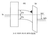
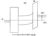
도 8a는 양의 전압(VG > 0)이 게이트(GE1)에 인가되는 상태를 예시하는 도면이고, 도 8b는 음의 전압(VG < 0)이 게이트(GE1)에 인가되는 상태를 예시하는 도면이다.
도 9는 진공 레벨 및 금속의 일함수(φM) 사이의 관계 및 진공 레벨과 산화물 반도체의 전자 친화도(χ) 사이의 관계를 예시하는 도면이다.
도 10은 C-V 특성들을 예시하는 도면이다.
도 11은 Vg 및 (1/C)2 사이의 관계를 예시하는 도면이다.
도 12는 반도체 장치를 예시하기 위한 횡단면도이다.
도 13a 및 도 13b는 각각 반도체 장치를 예시하기 위한 횡단면도이다.
도 14a 및 도 14b는 각각 반도체 장치를 예시하기 위한 횡단면도이다.
도 15a 및 도 15b는 각각 반도체 장치를 예시하기 위한 횡단면도이다.
도 16은 메모리 소자를 예시하기 위한 회로도이다.
도 17은 반도체 장치를 예시하기 위한 회로도이다.
도 18은 판독 회로를 예시하기 위한 회로도이다.
도 19는 메모리 소자를 예시하기 위한 회로도이다.
도 20a 내지 도 20f는 각각 전자 제품을 예시하기 위한 도면이다.1 is a circuit diagram for illustrating a semiconductor device.
2A and 2B are a cross-sectional view and a plan view for illustrating a semiconductor device.
3A to 3H are cross-sectional views for illustrating manufacturing steps of a semiconductor device.
4 (a) to 4 (g) are cross-sectional views for illustrating manufacturing steps of the semiconductor device.
5 (a) to 5 (d) are cross-sectional views for illustrating manufacturing steps of a semiconductor device.
6 is a cross-sectional view of a transistor including an oxide semiconductor.
Fig. 7 is an energy band diagram (schematic diagram) along the section A-A 'of Fig.
Figure 8a is a view illustrating a state in which the voltage (VG> 0) of the amount applied to the gate (GE1), Figure 8b illustrates the state a negative voltage (VG <0) is applied to the gate (GE1) FIG.
9 is a diagram illustrating the relationship between the vacuum level and the work function?M of the metal and the relationship between the vacuum level and the electron affinity (?) Of the oxide semiconductor.
Figure 10 is a diagram illustrating CV characteristics.
11 is a diagram illustrating the relationship between Vg and (1 / C)2 .
12 is a cross-sectional view for illustrating a semiconductor device.
13A and 13B are cross-sectional views for illustrating a semiconductor device, respectively.
14A and 14B are cross-sectional views for illustrating a semiconductor device, respectively.
15A and 15B are cross-sectional views for illustrating a semiconductor device, respectively.
16 is a circuit diagram for illustrating a memory element.
17 is a circuit diagram for illustrating a semiconductor device.
18 is a circuit diagram for illustrating a readout circuit.
19 is a circuit diagram for illustrating a memory device.
20A to 20F are views for illustrating electronic products, respectively.
본 발명의 실시 형태들의 예들은 첨부 도면들을 참조하여 하기에 기술될 것이다. 본 발명이 후속하는 설명에 제한되는 것이 아니라는 점에 유의하며, 여기서 개시된 모드들 및 상세항목들이 본 발명의 범위 및 사상으로부터 벗어나지 않고 다양한 방식들로 수정될 수 있다는 점이 쉽게 이해된다. 따라서, 본 발명은 여기에 포함된 실시 형태들의 내용에 제한되는 것으로서 해석되지 않아야 한다.Examples of embodiments of the present invention will be described below with reference to the accompanying drawings. It is to be noted that the present invention is not limited to the following description, and it is to be understood that the modes and details disclosed herein may be modified in various ways without departing from the scope and spirit of the present invention. Accordingly, the invention should not be construed as being limited to the contents of the embodiments contained herein.
도면 등에 예시된 각각의 구조의 위치, 사이즈, 범위 등이 용이한 이해를 위해 일부 경우들에서 정확하게 표현되지 않는다는 점에 유의한다. 따라서, 본 발명의 실시 형태들은 도면 등에서 개시된 이러한 위치, 사이즈, 범위 등에 반드시 제한되지는 않는다.It should be noted that the position, size, range, etc. of each structure illustrated in the drawings and the like are not accurately represented in some cases for easy understanding. Therefore, the embodiments of the present invention are not necessarily limited to such a position, size, range, etc. disclosed in drawings and the like.
본 명세서 등에서, "제1", "제2", "제3"과 같은 서수는 구성요소들 간의 혼돈을 회피하기 위해 사용되며, 상기 용어들은 구성요소들의 수의 제한을 의미하지는 않는다.In the present specification and the like, ordinal numbers such as "first", "second", "third" are used to avoid confusion among components, and these terms do not mean a limitation of the number of components.
(실시 형태 1)(Embodiment 1)
이러한 실시 형태에서, 개시된 발명의 일 실시 형태에 따른 반도체 장치의 구조들 및 제조 방법들은 도 1, 도 2a 및 도 2b, 도 3a 내지 도 3h, 도 4의 (a) 내지 (g), 도 5의 (a) 내지 (d), 도 6, 도 7, 도 8a 및 도 8b, 도 9, 도 10, 도 11, 도 12, 도 13a 및 도 13b, 도 14a 및 도 14b, 도 15a 및 도 15b를 참조하여 설명한다.In this embodiment, the structures and fabrication methods of the semiconductor device according to one embodiment of the disclosed invention are shown in Figs. 1, 2A and 2B, 3A to 3H, 4A to 4G, 5 6, 7, 8A and 8B, 9, 10, 11, 12, 13A and 13B, 14A and 14B, 15A and 15B .
<반도체 장치의 회로 구조><Circuit Structure of Semiconductor Device>
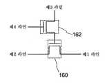
도 1은 반도체 장치의 회로 구조의 예를 예시한다. 반도체 장치는 산화물 반도체가 아닌 재료를 사용하는 트랜지스터(160) 및 산화물 반도체를 사용하는 트랜지스터(162)를 포함한다.1 illustrates an example of a circuit structure of a semiconductor device. The semiconductor device includes a
여기서, 트랜지스터(160)의 게이트 전극은 트랜지스터(162)의 소스 전극 및 드레인 전극 중 하나에 전기적으로 접속된다. 제1 배선("제1 라인"으로서 표기되며 또한 소스 라인이라 칭함) 및 제2 배선("제2 라인"으로서 표기되며 또한 비트 라인이라 칭함)은 각각 트랜지스터(160)의 소스 전극 및 트랜지스터(160)의 드레인 전극에 전기적으로 접속된다. 또한, 제3 배선("제3 라인"으로서 표기되며 또한 제1 신호 라인이라 칭함) 및 제4 배선("제4 라인"으로서 표기되며 또한 제2 신호 라인이라 칭함)은 각각, 트랜지스터(162)의 소스 전극 및 드레인 전극 중 다른 하나 및 트랜지스터(162)의 게이트 전극에 전기적으로 접속된다.Here, the gate electrode of the
산화물 반도체가 아닌 재료를 사용하는 트랜지스터(160)는 산화물 반도체를 사용하는 트랜지스터보다 훨씬 빠른 속도로 동작할 수 있고, 따라서, 저장된 데이터 등의 고속 판독을 달성한다. 또한, 오프 전류는 산화물 반도체를 사용하는 트랜지스터(162)에서 극도로 작다. 따라서, 트랜지스터(162)가 턴오프되는 경우, 트랜지스터(160)의 게이트 전극의 전위는 매우 긴 시간 동안 유지될 수 있다.The
게이트 전극의 전위가 매우 오랜 시간 동안 유지될 수 있다는 장점은 정보의 기입, 유지 및 판독이 하기에 기술되는 바와 같이 수행되도록 한다.The advantage that the potential of the gate electrode can be maintained for a very long time allows the writing, maintaining and reading of information to be performed as described below.
먼저, 정보를 기입 및 유지하는 것에 대한 설명이 이루어진다. 먼저, 제4 배선의 전위는 트랜지스터(162)가 온 상태가 되도록 하는 전위로 설정되고, 이에 의해 트랜지스터(162)는 온 상태에 있게 된다. 따라서, 제3 배선의 전위가 트랜지스터(160)의 게이트 전극에 인가된다(정보의 기입). 이후, 제4 배선의 전위는 트랜지스터(162)가 오프 상태가 되도록 하는 전위로 설정되며, 이에 의해 트랜지스터는 오프 상태에 있게 되고, 따라서, 트랜지스터(160)의 게이트 전극의 전위가 유지된다(정보의 유지).First, a description of writing and maintaining information is made. First, the potential of the fourth wiring is set to a potential which causes the
트랜지스터(162)의 오프 전류가 매우 작으므로, 트랜지스터(160)의 게이트 전극의 전위는 오랜 시간 동안 유지된다. 예를 들어, 트랜지스터(160)의 게이트 전극의 전위가 트랜지스터(160)가 온 상태가 되게 하는 전위인 경우, 트랜지스터(160)의 온 상태는 오랜 시간 동안 유지된다. 트랜지스터(160)의 게이트 전극의 전위가 트랜지스터(160)가 오프 상태가 되게 하는 전위인 경우, 트랜지스터(160)의 오프 상태는 오랜 시간 동안 유지된다.Since the off current of the
다음으로, 정보의 판독에 대한 설명이 이루어진다. 트랜지스터(160)의 온 상태 또는 오프 상태가 전술된 바와 같이 유지되고, 미리 결정된 전위(저 전위)가 제1 배선에 인가되는 경우, 제2 배선의 전위 값은 온 상태 또는 오프 상태인 트랜지스터(160)의 상태에 따라 변경된다. 예를 들어, 트랜지스터(160)가 온 상태인 경우, 제2 배선의 전위는 제1 배선의 전위에 의해 영향을 받음으로써 낮아진다. 반면, 트랜지스터(160)가 오프 상태인 경우, 제2 배선의 전위는 변경되지 않는다.Next, a description of reading of information is made. When the ON state or the OFF state of the
이러한 방식으로, 정보가 유지되는 상태에서 제1 배선의 전위를 제2 배선의 전위와 비교함으로써, 정보가 판독될 수 있다.In this manner, the information can be read by comparing the potential of the first wiring with the potential of the second wiring while the information is held.
이후, 정보의 재기입에 대한 설명이 이루어진다. 정보의 재기입은 전술된 정보의 기입 및 유지의 방식과 마찬가지 방식으로 수행된다. 즉, 제4 배선의 전위는 트랜지스터(162)가 온 상태가 되게 하는 전위로 설정되며, 이에 의해, 트랜지스터(162)는 온 상태에 있게 된다. 따라서, 제3 배선의 전위(새로운 정보에 관련된 전위)가 트랜지스터(160)의 게이트 전극에 인가된다. 이후, 제4 배선의 전위가 트랜지스터(162)가 오프 상태가 되게 하는 전위로 설정되며, 이에 의해 트랜지스터(162)는 오프 상태에 있게 되고, 따라서, 새로운 정보가 유지된다.Thereafter, the rewriting of the information is explained. The rewriting of information is performed in a manner similar to the manner of writing and maintaining the information described above. In other words, the potential of the fourth wiring is set to the potential for turning on the
전술된 바와 같이, 개시된 발명의 일 실시 형태에 따른 반도체 장치에서, 정보 기입을 다시 수행함으로써 정보가 직접 재기입될 수 있다. 따라서, 플래시 메모리 등에서 필요한 소거 동작이 요구되지 않으며, 따라서, 소거 동작으로 인한 동작 속도의 감소가 억제될 수 있다. 다시 말해, 반도체 장치의 고속 동작이 달성된다.As described above, in the semiconductor device according to the embodiment of the disclosed invention, the information can be directly rewritten by performing the information writing again. Therefore, a necessary erase operation is not required in the flash memory or the like, and therefore, the decrease in the operation speed due to the erase operation can be suppressed. In other words, a high-speed operation of the semiconductor device is achieved.
위의 기재에서, 캐리어로서 전자를 사용하는 n-타입 트랜지스터(n-채널 트랜지스터)가 사용되지만, 캐리어로서 정공을 사용하는 p-채널 트랜지스터가, n-채널 트랜지스터 대신 물론 사용될 수 있다는 점에 유의한다.Note that, in the above description, an n-type transistor (n-channel transistor) using electrons as a carrier is used, but a p-channel transistor using holes as a carrier can be used instead of an n-channel transistor .
<반도체 구조의 평면 구조 및 횡단면 구조>≪ Planar structure and cross-sectional structure of semiconductor structure >
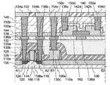
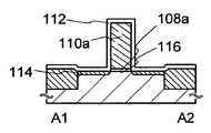
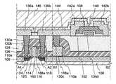
위의 반도체 장치의 구조의 예가 도 2a 및 도 2b에 예시된다. 도 2a 및 도 2b는 각각 반도체 장치의 횡단면도 및 평면도이다. 여기서, 도 2a는 도 2b의 라인 A1-A2 및 라인 B1-B2를 따라 취해지는 횡단면에 대응한다. 도 2a 및 도 2b에 예시된 반도체 장치는 하위 부분에 산화물 반도체가 아닌 재료를 사용하는 트랜지스터(160) 및 상위 부분에 산화물 반도체를 사용하는 트랜지스터(162)를 포함한다. n-채널 트랜지스터들이 트랜지스터들(160 및 162)로서 기술되지만, p-채널 트랜지스터들이 사용될 수 있다는 점에 유의한다. 특히, 트랜지스터(160)로서 p-채널 트랜지스터를 사용하는 것이 용이하다.An example of the structure of the above semiconductor device is illustrated in Figs. 2A and 2B. 2A and 2B are a cross-sectional view and a plan view of the semiconductor device, respectively. Here, Figure 2a corresponds to the cross-section taken along lines A1-A2 and B1-B2 in Figure 2b. The semiconductor device illustrated in Figs. 2A and 2B includes a
트랜지스터(160)는: 반도체 재료를 포함하는 기판(100)에 대해 제공되는 채널 형성 영역(116); 채널 형성 영역(116)이 사이에 개재되는 불순물 영역들(114) 및 채널 형성 영역(116)이 사이에 개재되는 고농도 불순물 영역들(120)(이는 또한 총체적으로 불순물 영역이라 칭함); 채널 형성 영역(116) 위에 제공되는 게이트 절연층(108a); 게이트 절연층(108a) 위에 제공되는 게이트 전극(110a); 및 불순물 영역들(114)에 전기적으로 접속되는 소스 또는 드레인 전극(130a) 및 소스 또는 드레인 전극(130b)을 포함한다.
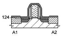
여기서, 측벽 절연층들(118)이 게이트 전극(110a)의 측면 표면들에 제공된다. 또한, 평면도로 볼 때 측벽 절연층들(118)과 겹치지 않는 기판(100)의 영역들에, 고농도 불순물 영역들(120)이 제공된다. 금속 화합물 영역들(124)은 고농도 불순물 영역들(120) 위에 있다. 기판(100) 위에서, 소자 격리 절연층(106)은 트랜지스터(160)를 둘러싸도록 제공되고, 층간 절연층(126) 및 층간 절연층(128)은 트랜지스터(160)를 피복하도록 제공된다. 소스 또는 드레인 전극(130a) 및 소스 또는 드레인 전극(130b)은 층간 절연층들(126 및 128)에 형성된 개구들을 통해 금속 화합물 영역들(124)에 전기적으로 접속된다. 다시 말해, 소스 또는 드레인 전극(130a) 및 소스 또는 드레인 전극(130b)은 금속 화합물 영역들(124)을 통해 고농도 불순물 영역들(120) 및 불순물 영역들(114)에 전기적으로 접속된다. 또한, 게이트 전극(110a)은 소스 또는 드레인 전극(130a) 및 소스 또는 드레인 전극(130b)과 마찬가지 방식으로 제공되는 전극(130c)에 전기적으로 접속된다.Here,
트랜지스터(162)는, 층간 절연층(128) 위에 제공되는 게이트 전극(136d); 게이트 전극(136d) 위에 제공되는 게이트 절연층(138); 게이트 절연층(138) 위에 제공되는 산화물 반도체층(140); 및 산화물 반도체층(140) 위에 제공되며 이 산화물 반도체층에 전기적으로 접속되는 소스 또는 드레인 전극(142a) 및 소스 또는 드레인 전극(142b)을 포함한다.The
여기서, 게이트 전극(136d)은 층간 절연층(128) 위에 형성되는 절연층(132)에 포함되도록 제공된다. 또한, 게이트 전극(136d)과 마찬가지로, 전극(136a), 전극(136b) 및 전극(136c)은 각각 소스 또는 드레인 전극(130a), 소스 또는 드레인 전극(130b), 및 전극(130c)에 접하여 형성된다.Here, the
트랜지스터(162) 위에, 보호 절연층(144)이 산화물 반도체층(140)의 일부분과 접하여 제공된다. 층간 절연층(146)은 보호 절연층(144) 위에 제공된다. 여기서, 보호 절연층(144) 및 층간 절연층(146)에서, 소스 또는 드레인 전극(142a) 및 소스 또는 드레인 전극(142b)에 도달하는 개구들이 형성된다. 개구들에서, 전극(150d) 및 전극(150e)이 각각 소스 또는 드레인 전극(142a) 및 소스 또는 드레인 전극(142b)과 접하도록 형성된다. 전극들(150d 및 150e)과 마찬가지로, 전극(150a), 전극(150b), 및 전극(150c)은 게이트 절연층(138), 보호 절연층(144) 및 층간 절연층(146)에서 제공되는 개구들에서, 각각, 전극(136a), 전극(136b) 및 전극(136c)과 접하도록 형성된다.On the
여기서, 산화물 반도체층(140)은 바람직하게는 수소와 같은 불순물을 제거함으로써 고순도화된 산화물 반도체이다. 구체적으로, 산화물 반도체층(140)에서의 수소 농도는 5 x 10¹⁹ 원자/cm3이하이고, 바람직하게는 5 x 10¹⁸ 원자/cm3이하이고, 더 바람직하게는 5 x 10¹⁷ 원자/cm3이하이다. 산화물 반도체층(140)은 바람직하게는 산소 부족으로 초래된 결함들이 충분한 산소를 포함함으로써 감소되는 산화물 반도체층이다. 수소 농도가 충분히 감소되고 산소 부족으로 초래된 결함들이 감소한 고순도화된 산화물 반도체층(140)에서, 캐리어 농도는 1 x 10¹²/cm3 이하이고, 바람직하게는 1 x 10¹¹/cm3 이하이다. 이러한 방식으로, i-타입(진성) 산화물 반도체 또는 실질적으로 i-타입 산화물 반도체가 되도록 만들어지는 산화물 반도체를 사용함으로써, 매우 적절한 오프 전류 특성들을 갖는 트랜지스터(162)가 획득될 수 있다. 예를 들어, 드레인 전압 Vd는 +1V 또는 +10V이고, 게이트 전압 Vg는 -5 V 내지 -20 V를 범위로 하고, 오프 전류는 1 x 10-13A 이하이다. 수소 농도가 충분히 감소하고 산소 부족으로 초래된 결함들이 감소한 고순도화된 산화물 반도체층(140)이 사용되고, 트랜지스터(162)의 오프 전류가 감소하는 경우, 신규한 구조를 갖는 반도체 장치가 구현된다. 산화물 반도체층(140) 내의 수소 농도가 2차 이온 질량 분석(SIMS)에 의해 측정되었다는 점에 유의한다.Here, the
또한, 절연층(152)은 층간 절연층(146) 위에 제공된다. 전극(154a), 전극(154b), 전극(154c) 및 전극(154d)은 절연층(152)에 포함되도록 제공된다. 여기서, 전극(154a)은 전극(150a)에 접하고, 전극(154b)은 전극(150b)에 접하고, 전극(154c)은 전극(150c 및 150d)에 접하고, 전극(154d)은 전극(150e)에 접한다.Further, an insulating
즉, 도 2a 및 도 2b에 예시된 반도체 장치에서, 트랜지스터(160)의 게이트 전극(110a)은 전극들(130c, 136c, 150c, 154c, 및 150d)을 통해 트랜지스터(162)의 소스 또는 드레인 전극(142a)에 전기적으로 접속된다.2A and 2B, the
<반도체 장치를 제조하기 위한 방법>≪ Method for manufacturing semiconductor device >
다음으로, 전술된 반도체 장치를 제조하기 위한 방법이 기술될 것이다. 먼저, 하위 부분에 트랜지스터(160)를 제조하기 위한 방법이 도 3a 내지 도 3h를 참조하여 기술될 것이고, 이후, 상위 부분에 트랜지스터(162)를 제조하기 위한 방법이 도 4의 (a) 내지 (g) 및 도 5의 (a) 내지 (d)를 참조하여 기술될 것이다.Next, a method for manufacturing the above-described semiconductor device will be described. First, a method for fabricating the
<하위 부분에 트랜지스터를 제조하기 위한 방법>≪ Method for manufacturing a transistor in a lower portion >
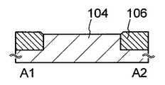
먼저, 반도체 재료를 포함하는 기판(100)이 준비된다(도 3a를 참조). 기판(100)이 반도체 재료를 포함함에 따라, 실리콘, 실리콘 탄화물 등을 포함하는 단결정 반도체 기판 또는 다결정 반도체 기판, 실리콘 게르마늄 등을 포함하는 화합물 반도체 기판, SOI 기판 등이 사용될 수 있다. 여기서, 단결정 실리콘 기판이 반도체 재료를 포함하는 기판(100)으로서 사용되는 예가 기술된다. 일반적으로, 용어 "SOI 기판"이 자신의 절연 표면 위에 실리콘 반도체층을 갖는 기판을 의미한다는 점에 유의한다. 본 명세서 등에서, 용어 "SOI 기판"은 또한, 자신의 절연 표면 위에 실리콘이 아닌 재료를 사용하는 반도체층을 갖는 기판을 의미한다. 다시 말해, "SOI 기판"에 포함된 반도체층은 실리콘 반도체층에 제한되지 않는다. SOI 기판의 예들은 유리 기판과 같은 절연 기판 위에 반도체층을 갖고, 반도체층 및 절연 기판 사이에 절연층이 있는 기판을 포함한다.First, a
기판(100) 위에, 소자 분리 절연층을 형성하는 마스크로서 기능하는 보호층(102)이 존재한다(도 3a 참조). 보호층(102)으로서, 예를 들어, 산화 실리콘, 질화 실리콘, 질화 산화 실리콘 등을 사용하여 형성되는 절연층이 사용될 수 있다. 트랜지스터의 임계 전압이 제어되도록 위 단계 전에 또는 후에 n-타입 도전성을 주는 불순물 원소 또는 p-타입 도전성을 주는 불순물 원소가 기판(100)에 추가될 수 있다는 점에 유의한다. 기판(100)에 포함된 반도체 재료가 실리콘인 경우 n-타입 도전성을 주는 불순물로서, 인, 비소 등이 사용될 수 있다. p-타입 도전성을 주는 불순물로서, 예를 들어, 붕소, 알루미늄, 갈륨 등이 사용될 수 있다.On the
다음으로, 마스크로서 위의 보호층(102)을 사용하면, 보호층(102)으로 피복되지 않은 영역(노출된 영역) 내의 기판(100)의 일부분이 에칭에 의해 제거된다. 따라서, 격리된 반도체 영역(104)이 형성된다(도 3b 참조). 에칭에 대해, 건식 에칭이 바람직하게 수행되지만, 습식 에칭이 수행될 수도 있다. 에칭 가스 및 에천트는 에칭될 대상의 재료에 따라 적절한 것으로 선택될 수 있다.Next, using the
다음으로, 절연층은 반도체 영역(104)을 피복하도록 형성되며, 반도체 영역(104)과 겹치는 영역 내에서 선택적으로 제거되며, 이에 의해 소자 격리 절연층(106)이 형성된다(도 3b 참조). 절연층은 산화 실리콘, 질화 실리콘, 질화 산화 실리콘 등을 사용하여 형성된다. 절연층을 제거하기 위한 방법으로서, CMP와 같은 연마 처리 및 에칭 처리가 존재하며, 이들 중 임의의 것이 사용될 수 있다. 반도체 영역(104)이 형성된 이후, 또는 소자 격리 절연층(106)이 형성된 이후, 보호층(102)이 제거될 수 있다는 점에 유의한다.Next, an insulating layer is formed to cover the
이후, 절연층은 반도체 영역(104) 위에 형성되고, 도전성 재료를 포함하는 층은 절연층 위에 형성된다.Then, an insulating layer is formed on the
절연층은 추후에 절연층으로서의 역할을 하며, 바람직하게는, CVD법에 의해 획득되는, 산화 실리콘, 질화 산화 실리콘, 질화 실리콘, 산화 하프늄, 산화 알루미늄, 산화 탄탈륨 등을 포함하는 막을 사용하는 단층 구조 또는 적층 구조를 가진다. 대안적으로, 위의 절연층은 고밀도 플라즈마 처리 또는 열산화 처리에 의해 반도체 영역(104)의 표면을 산화 또는 질화시킴으로써 형성될 수 있다. 고밀도 플라즈마 처리는, 예를 들어, 헬륨, 아르곤, 크립톤 또는 제논과 같은 혼합 가스 및 산소, 산화 질소, 암모니아, 질소 또는 수소와 같은 가스를 사용하여 수행될 수 있다. 절연층의 두께는 특별히 제한되지 않지만, 예를 들어, 1nm 이상 100nm 이하일 수 있다.The insulating layer serves as an insulating layer in the future and preferably has a single-layer structure using a film containing silicon oxide, silicon nitride oxide, silicon nitride, hafnium oxide, aluminum oxide, tantalum oxide, or the like, Or a laminated structure. Alternatively, the above insulating layer can be formed by oxidizing or nitriding the surface of the
도전성 재료를 포함하는 층은 알루미늄, 구리, 티타늄, 탄탈륨 또는 텅스텐 등의 금속 재료를 사용하여 형성될 수 있다. 대안적으로, 도전성 재료를 포함하는 층은 도전성 재료를 포함하는 다결정 실리콘과 같은 반도체 재료를 사용하여 형성될 수 있다. 또한, 도전성 재료를 포함하는 층을 형성하기 위한 방법은 특별히 제한되지 않으며, 증착법, CVD법, 스퍼터링법 및 스핀 코팅법과 같은 다양한 성막 방법들 중 임의의 방법이 적용가능하다. 이러한 실시 형태에서, 도전성 재료를 포함하는 층이 금속 재료를 사용하여 형성되는 경우의 예가 기술된다.The layer containing the conductive material may be formed using a metal material such as aluminum, copper, titanium, tantalum or tungsten. Alternatively, the layer including the conductive material may be formed using a semiconductor material such as polycrystalline silicon including a conductive material. Further, the method for forming the layer containing a conductive material is not particularly limited, and any of various deposition methods such as a deposition method, a CVD method, a sputtering method and a spin coating method is applicable. In this embodiment, an example in which a layer including a conductive material is formed using a metal material is described.
이후, 절연층 및 도전성 재료를 포함하는 층을 선택적으로 에칭시킴으로써, 게이트 절연층(108a) 및 게이트 전극(110a)이 형성된다(도 3c 참조).Thereafter, the
다음으로, 게이트 전극(110a)을 피복하는 절연층(112)이 형성된다(도 3c 참조). 이후, 인(P), 비소(As) 등이 반도체 영역(104)에 첨가되고, 이에 의해, 얕은 접합 깊이를 갖는 불순물 영역(114)들이 형성된다(도 3c 참조). n-채널 트랜지스터가 형성되도록 인 또는 비소가 여기에 첨가되지만, p-채널 트랜지스터를 형성하는 경우, 붕소(B) 또는 알루미늄(Al)과 같은 불순물 원소가 첨가될 수 있다는 점에 유의한다. 또한, 채널 형성 영역(116)이 불순물 영역(114)의 형성에 의해 게이트 절연층(108a) 아래의 반도체 영역(104) 내에 형성된다는 점에 유의한다(도 3c 참조). 여기서, 추가된 불순물의 농도는 적절하게 설정될 수 있고, 반도체 소자가 매우 소형화되는 경우, 농도는 바람직하게는 높도록 설정된다. 또한, 절연층(112)이 불순물 영역들(114)의 형성 이후 형성되는 프로세스가, 불순물 영역들(114)이 절연층(112)의 형성 이후 형성되는 여기서 사용되는 프로세스 대신 사용될 수 있다.Next, an insulating
이후, 측벽 절연층들(118)이 형성된다(도 3d 참조). 절연층은 절연층(112)을 피복하도록 형성되고, 이후, 고 이방성 에칭 처리를 받으며, 이에 의해, 측벽 절연층들(118)은 자가-정렬 방식으로 형성될 수 있다. 게이트 전극(110a)의 상면 및 불순물 영역들(114)의 상면들이 노출되도록, 이때 절연층(112)이 부분적으로 에칭되는 것이 바람직하다.Then, sidewall insulating
이후, 절연층은 게이트 전극(110a), 불순물 영역들(114), 측벽 절연층들(118) 등을 피복하도록 형성된다. 인(P), 비소(As) 등은 이후 절연층이 불순물 영역들(114)과 접하는 영역들에 추가되며, 이에 의해, 고농도 불순물 영역들(120)이 형성된다(도 3e 참조). 다음으로, 위의 절연층이 제거되고, 게이트 전극(110a), 측벽 절연층들(118), 고농도 불순물 영역들(120) 등을 피복하도록 금속층(122)이 형성된다(도 3e 참조). 진공 증착법, 스퍼터링법, 및 스핀 코팅법과 같은 다양한 방법들 중 임의의 방법이 금속층(122)의 형성에 적용가능하다. 낮은 저항을 갖는 금속 화합물을 형성하기 위해 반도체 영역(104) 내에 포함되는 반도체 재료와 반응하는 금속 재료를 사용하여 금속층(122)이 형성되는 것이 바람직하다. 이러한 금속 재료의 예들은 티타늄, 탄탈륨, 텅스텐, 니켈, 코발트 및 플래티늄을 포함한다.Then, an insulating layer is formed to cover the
다음으로, 열처리가 수행되며, 이에 의해 금속층(122)이 반도체 재료와 반응한다. 따라서, 고농도 불순물 영역들(120)과 접하는 금속 화합물 영역들(124)이 형성된다(도 3f 참조). 게이트 전극(110a)에 대해 다결정 실리콘을 사용하는 경우, 금속층(122)과 접하는 게이트 전극(110a)의 일부분이 또한 금속 화합물 영역을 가진다는 점에 유의한다.Next, a heat treatment is performed, whereby the
열처리로서, 플래시 램프를 이용한 조사(irradiation)가 사용된다. 다른 열처리 방법이 당연히 사용될 수도 있지만, 매우 짧은 시간 동안의 열처리를 달성할 수 있는 방법이 바람직하게는 금속 화합물의 형성 시 화학 반응의 제어가능성을 개선하기 위해 사용된다. 위의 금속 화합물 영역들이 금속 재료와 반도체 재료와의 반응을 통해 형성되며, 충분히 증가한 도전성을 가진다는 점에 유의한다. 금속 화합물 영역들의 형성에 의해, 전기 저항이 충분히 감소할 수 있으며, 소자 특성들이 개선될 수 있다. 금속층(122)은 금속 화합물 영역들(124)의 형성 이후 제거된다.As the heat treatment, irradiation using a flash lamp is used. Although other heat treatment methods may of course be used, a method capable of achieving a heat treatment for a very short period of time is preferably used to improve the controllability of the chemical reaction during the formation of the metal compound. Note that the above metal compound regions are formed through the reaction of the metal material and the semiconductor material, and have sufficiently increased conductivity. By forming the metal compound regions, the electrical resistance can be sufficiently reduced, and the device characteristics can be improved. The
층간 절연층들(126 및 128)은 위의 단계들에서 형성된 구성요소들을 피복하기 위해 형성된다(도 3g 참조). 층간 절연층들(126 및 128)은 산화 실리콘, 질화 산화 실리콘, 질화 실리콘, 산화 하프늄, 산화 알루미늄 또는 산화 탄탈륨과 같은 무기 절연 재료를 포함하는 재료를 사용하여 형성될 수 있다. 대안적으로, 폴리이미드 또는 아크릴과 같은 유기 절연 재료가 사용될 수 있다. 층간 절연층(126) 및 층간 절연층(128)이 여기서 2-층 구조를 형성하지만, 층간 절연층들의 구조가 이에 제한되지 않는다는 점에 유의한다. 또한, 층간 절연층(128)의 표면이, 층간 절연층(128)이 형성된 후 평탄화되도록, 바람직하게는 CMP, 에칭 등을 받을 수 있다.
이후, 금속 화합물 영역들(124)에 도달하는 개구들이 층간 절연층들에 형성되고, 이후 소스 또는 드레인 전극(130a) 및 소스 또는 드레인 전극(130b)이 개구들에 형성된다(도 3h 참조). 예를 들어, 소스 또는 드레인 전극(130a) 및 소스 또는 드레인 전극(130b)이 다음과 같이 형성될 수 있다: PVD법, CVD법 등에 의해 개구들을 포함하는 영역 내에 도전층이 형성된다; 이후, 도전층의 일부가 에칭, CMP 등에 의해 제거된다.Then, openings reaching the
도전층의 일부를 제거함으로써 소스 또는 드레인 전극(130a) 및 소스 또는 드레인 전극(130b)을 형성하는 경우, 그 표면들이 바람직하게는 평평해지도록 처리된다는 점에 유의한다. 예를 들어, 티타늄막, 질화 티타늄막 등이 개구들을 포함하는 영역에서 작은 두께를 가지도록 형성되고, 이후 개구들에 포함되도록 텅스텐 막이 형성되는 경우, 그 후 수행되는 CMP는 텅스텐 막, 티타늄 막, 질화 티타늄막 등의 불필요한 부분을 제거할 수 있고 표면의 평탄성을 개선할 수 있다. 전술된 바와 같은 소스 또는 드레인 전극(130a) 및 소스 또는 드레인 전극(130b)의 표면들을 포함하는 표면들을 평탄화함으로써, 적절한 전극, 배선, 절연층, 반도체층 등이 추후 단계에서 형성될 수 있다.Note that when the source or
오직 금속 화합물 영역들(124)과 접하는 소스 또는 드레인 전극(130a) 및 소스 또는 드레인 전극(130b)만이 기술되지만, 게이트 전극(110a)(예를 들어, 도 2a의 전극(130c)) 등과 접하는 전극이 동일한 단계에서 형성될 수 있다는 점에 유의한다. 소스 또는 드레인 전극(130a) 및 소스 또는 드레인 전극(130b)에 대해 사용되는 재료는 특별히 제한되지 않으며, 다양한 도전성 재료들 중 임의의 재료가 사용될 수 있다. 예를 들어, 몰리브덴, 티타늄, 크롬, 탄탈륨, 텅스텐, 알루미늄, 구리, 네오디뮴 또는 스칸듐과 같은 도전성 재료가 사용될 수 있다.Only the source or
위의 프로세스를 통해, 반도체 재료를 포함하는 기판(100)을 사용하는 트랜지스터(160)가 형성된다. 전극, 배선, 절연층 등이 또한 위의 프로세스가 수행된 이후에 형성될 수 있다는 점에 유의한다. 층간 절연층 및 도전층이 적층되는 다층 배선 구조가 배선 구조로서 사용되는 경우, 고집적 반도체 장치가 제공될 수 있다.Through the above process, a
<상위 부분에서 트랜지스터를 제조하기 위한 방법>≪ Method for manufacturing a transistor in the upper part >
이후, 트랜지스터(162)가 층간 절연층(128) 위에 제조되는 프로세스가 도 4의 (a) 내지 (g) 및 도 5의 (a) 내지 (d)를 참조하여 기술된다. 트랜지스터(162) 아래에 있는 트랜지스터(160) 등이, 층간 절연층(128), 트랜지스터(162) 등에 대한 다양한 전극들의 제조 프로세스를 예시하는 도 4의 (a) 내지 (g) 및 도 5의 (a) 내지 (d)에서 생략된다는 점에 유의한다.The process by which the
먼저, 절연층(132)이 층간 절연층(128), 소스 또는 드레인 전극(130a), 소스 또는 드레인 전극(130b) 및 전극(130c) 위에 형성된다(도 4의 (a) 참조). 절연층(132)은 PVD법, CVD법 등에 의해 형성될 수 있다. 산화 실리콘, 질화 산화 실리콘, 질화 실리콘, 산화 하프늄, 산화 알루미늄, 또는 산화 탄탈륨과 같은 무기 절연 재료를 포함하는 재료가 절연층(132)에 대해 사용될 수 있다.First, an insulating
다음으로, 소스 또는 드레인 전극(130a), 소스 또는 드레인 전극(130b), 및 전극(130c)이 절연층(132)에 형성된다. 이때, 게이트 전극(136d)이 형성될 영역에 다른 개구가 형성된다. 도전층(134)은 개구들에 포함되도록 형성된다(도 4의 (b) 참조). 위의 개구들은 예를 들어, 마스크의 사용으로 에칭에 의해 형성될 수 있다. 마스크는 예를 들어, 포토마스크를 사용하여 노출에 의해 형성될 수 있다. 에칭에 대해, 습식 에칭 또는 건식 에칭이 수행될 수 있지만, 건식 에칭이 미세 패터닝의 견지에서 바람직하다. 도전층(134)은 PVD법 또는 CVD법 등의 성막 방법에 의해 형성될 수 있다. 도전층(134)에 대한 재료의 예들은 몰리브덴, 티타늄, 크롬, 탄탈륨, 텅스텐, 알루미늄, 구리, 네오디뮴 및 스칸듐과 같은 도전성 재료, 이들 중 임의의 것의 합금, 및 이들 중 임의의 것을 포함하는 화합물(예를 들어, 이들 중 임의의 것의 질화물)을 포함한다.Next, a source or
구체적으로, 예를 들어, 도전층(134)은 다음과 같이 형성될 수 있다: 티타늄 막은 개구들을 포함하는 영역 내에 PVD 법에 의해 작은 두께를 가지도록 형성되고, 질화 티타늄막은 이후 CVD 법에 의해 작은 두께를 가지도록 형성된다; 이후, 텅스텐 막이 개구들에 포함되도록 형성된다. 여기서, PVD법에 의해 형성되는 티타늄 막은 하위 전극(여기서, 소스 또는 드레인 전극(130a), 소스 또는 드레인 전극(130b), 전극(130c) 등)과의 계면에서 산화물 막을 감소시키는 기능을 가져서, 하위 전극과의 접촉 저항이 감소한다. 또한, 후속 형성되는 질화 티타늄막은 도전성 재료의 확산이 방지되도록 장벽 특징을 가진다. 또한, 장벽 막이 티타늄, 티타늄 질화물 등을 사용하여 형성된 후, 구리 막이 도금법에 의해 형성될 수 있다.Specifically, for example, the
도전층(134)이 형성된 후, 절연층(132)이 노출되도록 도전층(134)의 일부분이 에칭, CMP 등에 의해 제거되며, 전극들(136a, 136b, 및 136c) 및 게이트 전극(136d)이 형성된다(도 4의 (c) 참조). 전극들(136a, 136b, 및 136c) 및 게이트 전극(136d)이 위의 도전층(134)의 일부를 제거함으로써 형성되는 경우, 바람직하게는 평탄화된 표면들이 획득되도록 처리가 수행된다는 점에 유의한다. 절연층(132)의 표면들의 평탄화에 의해, 전극들(136a, 136b, 및 136c) 및 게이트 전극(136d), 바람직한 전극들, 배선들, 절연층들, 반도체층들 등이 추후 단계에서 수행될 수 있다.After the
이후, 게이트 절연층(138)은 절연층(132), 전극들(136a, 136b, 및 136c) 및 게이트 전극(136d)을 피복하도록 형성된다(도 4의 (d) 참조). 게이트 절연층(138)은 스퍼터링법, CVD법 등에 의해 형성될 수 있다. 게이트 절연층(138)은 바람직하게는 산화 실리콘, 질화 실리콘, 산화 질화 실리콘, 질화 산화 실리콘, 산화 알루미늄, 산화 하프늄, 산화 탄탈륨 등을 포함한다. 게이트 절연층(138)이 단층 구조 또는 적층 구조를 가질 수 있다는 점에 유의한다. 예를 들어, 산화 질화 실리콘의 게이트 절연층(138)은 소스 가스들로서 실란(SiH4), 산소 및 질소를 사용하는 플라즈마 CVD법에 의해 형성될 수 있다. 게이트 절연층(138)의 두께는 특별히 제한되지 않지만, 두께는, 예를 들어, 10 nm 이상 500nm 이하일 수 있다. 적층 구조가 사용되는 경우, 게이트 절연층(138)은 바람직하게는 50nm 이상 200nm 이하의 두께를 갖는 제1 게이트 절연층 및 제1 게이트 절연층 위에 5nm 이상 300nm 이하의 두께를 갖는 제2 게이트 절연층을 적층함으로써 수행된다.Thereafter, the
i-타입 산화물 반도체 또는 불순물을 제거함으로써 실질적으로 i-타입 산화물 반도체가 되도록 만들어진 산화물 반도체(고순도화된 산화물 반도체)가 계면 상태 또는 계면 전하에 대해 극도로 민감하며; 따라서, 이러한 산화물 반도체가 산화물 반도체층에 대해 사용되는 경우, 산화물 반도체층 및 게이트 절연층 사이의 계면이 중요하다는 점에 유의한다. 다시 말해, 고순도화된 산화물 반도체층과 접하는 게이트 절연층(138)은 고품질을 가질 필요가 있다.oxide semiconductors (high purity oxide semiconductors) made to be substantially i-type oxide semiconductors by removing i-type oxide semiconductors or impurities are extremely sensitive to interface states or interface charge; Therefore, when such an oxide semiconductor is used for the oxide semiconductor layer, it is noted that the interface between the oxide semiconductor layer and the gate insulating layer is important. In other words, the
예를 들어, 마이크로파(2.45 GHz)를 사용하는 고밀도 플라즈마 CVD법이 바람직한데, 왜냐하면, 높은 내전압을 갖는 밀도 높은 고품질 게이트 절연층(138)이 이에 의해 형성될 수 있기 때문이다. 이러한 방식으로, 계면 상태가 감소할 수 있으며, 고순도화된 산화물 반도체층 및 고품질의 게이트 절연층이 서로 접하는 경우 계면 특성들이 바람직할 수 있다.For example, a high density plasma CVD process using microwaves (2.45 GHz) is preferred because a dense, high quality
물론, 이러한 고순도화된 산화물 반도체층이 사용되는 경우라도, 양호한 품질을 갖는 절연층이 게이트 절연층으로서 형성될 수 있는 한, 스퍼터링법 또는 플라즈마 CVD법 등의 다른 방법이 사용될 수 있다. 대안적으로, 자신의 막 품질 및 산화물 반도체층과의 계면 특성들이 형성 후의 열처리에 의해 수정되는 절연막이 적용될 수 있다. 어느 경우든, 게이트 절연층(138)으로서 양호한 품질을 갖고, 양호한 계면이 형성되도록 게이트 절연층 및 산화물 반도체층 사이의 계면 상태 밀도를 감소시키는 층이 수용가능하다.Of course, even when such a high-purity oxide semiconductor layer is used, other methods such as a sputtering method or a plasma CVD method can be used as long as an insulating layer having a good quality can be formed as a gate insulating layer. Alternatively, an insulating film whose film quality and interfacial characteristics with the oxide semiconductor layer are modified by heat treatment after formation can be applied. In either case, a layer which has good quality as the
또한, 불순물이 산화물 반도체 내에 포함되는 경우, 2 x 10⁶ V/cm의 전계 강도를 갖고 12시간 동안 85℃에서의 바이어스 온도 시험(BT 시험)에서, 불순물과 산화물 반도체의 주성분 사이의 결합은 강한 전계(B: 바이어스) 및 고온(T: 온도)에 의해 절단(cut)되며 생성된 불포화 결합(dangling bond)은 임계 전압(Vth)의 시프트를 초래한다.Further, when the impurity is contained in the oxide semiconductor, the bond between the impurity and the main component of the oxide semiconductor has a strong electric field strength of 2 x 10⁶ V / cm and a bias temperature test (BT test) at 85 캜 for 12 hours The resulting dangling bond is cut by an electric field (B: bias) and a high temperature (T: temperature), resulting in a shift of the threshold voltage (Vth ).
반면, 개시된 발명의 일 실시 형태에 따라, BT 시험에서도 안정한 트랜지스터는 반도체 산화물에서 불순물, 특히, 수소 또는 물을 제거하고, 전술된 바와 같이 게이트 절연층 및 산화물 반도체층 사이의 양호한 계면 특성들을 구현함으로써 제공될 수 있다.On the other hand, according to one embodiment of the disclosed invention, in a BT test, a stable transistor is formed by removing impurities, particularly hydrogen or water, from the semiconductor oxide and realizing good interfacial characteristics between the gate insulating layer and the oxide semiconductor layer as described above Can be provided.
이후, 산화물 반도체층은 게이트 절연층(138) 위에 형성되고, 섬-형상을 갖는 산화물 반도체층(140)이 형성되도록 마스크를 사용하는 에칭과 같은 방법에 의해 처리된다(도 4의 (e) 참조).Thereafter, an oxide semiconductor layer is formed on the
산화물 반도체층으로서, In-Ga-Zn-O계 산화물 반도체층, In-Sn-Zn-O계 산화물 반도체층, In-Al-Zn-O계 산화물 반도체층, Sn-Ga-Zn-O계 산화물 반도체층, Al-Ga-Zn-O계 산화물 반도체층, Sn-Al-Zn-O계 산화물 반도체층, In-Zn-O계 산화물 반도체층, Sn-Zn-O계 산화물 반도체층, Al-Zn-O계 산화물 반도체층, In-O계 산화물 반도체층, Sn-O계 산화물 반도체층, 또는 Zn-O계 산화물 반도체층을 사용하는 것이 바람직하며, 특히 이는 바람직하게는 비정질이다. 이러한 실시 형태에서, 산화물 반도체층으로서, 비정질 산화물 반도체층은 막 형성을 위한 In-Ga-Zn-O계 산화물 반도체 타겟의 사용을 통해 스퍼터링 방법에 의해 형성된다. 비정질 산화물 반도체층에 실리콘을 추가함으로써, 결정화가 억제될 수 있고, 따라서, 산화물 반도체층이 2 wt.% 이상 10 wt.% 이하의 SiO2를 포함하는 타겟을 사용하여 형성될 수 있다는 점에 유의한다.Zn-O-based oxide semiconductor layer, an In-Sn-Zn-O-based oxide semiconductor layer, an In-Sn-Zn-O-based oxide semiconductor layer, Zn-O-based oxide semiconductor layer, Sn-Zn-O-based oxide semiconductor layer, Al-Zn-O-based oxide semiconductor layer, -O-based oxide semiconductor layer, an In-O-based oxide semiconductor layer, a Sn-O-based oxide semiconductor layer, or a Zn-O-based oxide semiconductor layer is preferably used. In this embodiment, as the oxide semiconductor layer, an amorphous oxide semiconductor layer is formed by a sputtering method through the use of an In-Ga-Zn-O-based oxide semiconductor target for film formation. It is noted that by adding silicon to the amorphous oxide semiconductor layer, the crystallization can be suppressed, and therefore, the oxide semiconductor layer can be formed using a target containing SiO2 at2 wt.% Or more and 10 wt.% Or less. do.
스퍼터링법을 이용하여 산화물 반도체층을 형성하기 위한 타겟으로서, 예를 들어, 자신의 주성분으로서 아연 산화물을 포함하는 금속 산화물 타겟이 사용될 수 있다. 또한, 예를 들어, In, Ga, 및 Zn(In2O3:Ga2O3:ZnO = 1:1:1[몰비] 또는 In:Ga:Zn = 1:1:0.5[원자비]의 조성비)을 포함하는 산화물 반도체를 성막하기 위한 타겟이 사용될 수 있다. 또한, (In:Ga:Zn = 1:1:1[원자비]의 조성비 또는 In:Ga:Zn = 1:1:2[원자비]를 갖는) In, Ga, 및 Zn을 포함하는 산화물 반도체를 성막하기 위한 타겟이 사용될 수 있다. 산화물 반도체를 성막하기 위한 타겟의 충전율은 90% 이상 100% 이하이고, 바람직하게는 95% 이상(예를 들어, 99.9%)이다. 충전율이 높은 산화물 반도체를 성막하기 위한 타겟을 사용함으로써, 밀도 높은 산화물 반도체층이 형성된다.As a target for forming the oxide semiconductor layer by the sputtering method, for example, a metal oxide target containing zinc oxide as its main component may be used. Also, for example, In, Ga, and Zn (In2 O3: 0.5 [atomicratio]: Ga 2 O 3: ZnO = 1: 1: 1 [ molar ratio] or In: Ga: Zn = 1: 1 A composition ratio) can be used as the target for forming the oxide semiconductor. In addition, an oxide semiconductor containing In, Ga, and Zn (having a composition ratio of In: Ga: Zn = 1: 1: 1 [atomic ratio] or In: Ga: Zn = 1: 1: 2 A target for film formation may be used. The filling rate of the target for forming the oxide semiconductor is 90% or more and 100% or less, preferably 95% or more (for example, 99.9%). By using a target for forming an oxide semiconductor having a high filling rate, a dense oxide semiconductor layer is formed.
산화물 반도체층을 형성하기 위한 대기(atmosphere)는 바람직하게는 희가스(통상적으로 아르곤) 대기, 산소 대기, 또는 희가스(통상적으로 아르곤)와 산소의 혼합된 대기이다. 구체적으로, 수소, 물, 수산기 및 수소화물과 같은 불순물의 농도가 대략 수 ppm(parts per million)(바람직하게는 수 ppb(parts per billion))으로 감소하는, 고순도의 가스가 바람직하다.The atmosphere for forming the oxide semiconductor layer is preferably a mixed atmosphere of rare gas (typically argon) atmosphere, oxygen atmosphere, or rare gas (typically argon) and oxygen. In particular, a high purity gas is preferred, in which the concentration of impurities such as hydrogen, water, hydroxyl, and hydrides is reduced to parts per million (preferably parts per billion).
산화물 반도체층의 형성 시점에서, 기판은 감소한 압력 상태에서 유지되는 처리 챔버에 고정되며, 기판 온도는 100℃ 이상이고 600℃ 이하이며, 바람직하게는 200℃ 이상이고 400℃ 이하이다. 기판이 가열되는 동안 산화물 반도체층이 형성되는 경우, 산화물 반도체층에 포함된 불순물들의 농도가 감소할 수 있다. 또한, 스퍼터링으로 인한 손상이 감소한다. 처리 챔버 내에서 유지되는 습기가 제거되는 동안 수소 및 습기를 제거한 스퍼터링 가스가 유입되고, 산화물 반도체층은 타겟으로서 금속 산화물의 사용을 통해 형성된다. 처리 챔버 내의 나머지 습기를 제거하기 위해, 바람직하게는 흡착형 진공 펌프가 사용된다. 예를 들어, 크라이오펌프, 이온 펌프, 또는 티타늄 승화 펌프가 사용될 수 있다. 배기 유닛은 콜드 트랩이 제공된 터보 펌프일 수 있다. 수소 원자, 물(H2O)과 같은 수소 원자를 포함하는 화합물(바람직하게는 탄소 원자를 포함하는 화합물) 등은 크라이오펌프를 이용하여 배기되는 성막 챔버로부터 제거되며, 이에 의해, 성막 챔버에 형성되는 산화물 반도체층에 포함되는 불순물의 농도가 감소할 수 있다.At the time of formation of the oxide semiconductor layer, the substrate is fixed to the processing chamber maintained at a reduced pressure state, and the substrate temperature is 100 DEG C or higher and 600 DEG C or lower, preferably 200 DEG C or higher and 400 DEG C or lower. When the oxide semiconductor layer is formed while the substrate is heated, the concentration of the impurities contained in the oxide semiconductor layer may decrease. In addition, damage due to sputtering is reduced. While the moisture retained in the processing chamber is removed, hydrogen and moisture-free sputtering gas is introduced, and the oxide semiconductor layer is formed through the use of a metal oxide as a target. To remove the remaining moisture in the processing chamber, an adsorption vacuum pump is preferably used. For example, a cryo pump, ion pump, or titanium sublimation pump may be used. The exhaust unit may be a turbo pump provided with a cold trap. A compound containing a hydrogen atom such as hydrogen atom or water (H2 O) (preferably a compound containing a carbon atom)) is removed from the film deposition chamber exhausted by using the cryopump, The concentration of the impurity contained in the oxide semiconductor layer to be formed can be reduced.
예를 들어, 성막 조건들이 다음과 같이 설정될 수 있다: 기판과 타겟 사이의 거리는 100mm이다; 압력은 0.6 Pa이다; 직류(DC) 전력은 0.5 kW이다; 대기는 산소 대기이다(산소 유량비는 100%). 파우더 재료들(입자 또는 먼지라고도 함)이 감소하고 막 두께의 변경이 적을 수 있으므로, 펄스식 직류 전원이 사용되는 것이 바람직하다. 산화물 반도체층의 두께는 2nm 이상 200 nm 이하이고, 바람직하게는 5 nm 이상 30 nm 이하이다. 적절한 두께는 도포된 산화물 반도체 재료에 따르며, 산화물 반도체층의 두께가 재료에 따라 적절하게 설정될 수 있다는 점에 유의한다.For example, deposition conditions may be set as follows: the distance between the substrate and the target is 100 mm; The pressure is 0.6 Pa; The direct current (DC) power is 0.5 kW; The atmosphere is oxygen atmosphere (oxygen flow ratio is 100%). It is preferable that a pulsed direct current power source be used because the powder materials (also referred to as particles or dust) may decrease and the film thickness change may be small. The thickness of the oxide semiconductor layer is 2 nm or more and 200 nm or less, preferably 5 nm or more and 30 nm or less. Note that an appropriate thickness depends on the applied oxide semiconductor material, and the thickness of the oxide semiconductor layer may be appropriately set depending on the material.
산화물 반도체층이 스퍼터링법에 의해 형성되기 전에, 게이트 절연층(138)의 표면에 부착된 먼지가 바람직하게는, 아르곤 가스가 유입되어 플라즈마가 생성되는 역 스퍼터링에 의해 제거된다는 점에 유의한다. 여기서, 역 스퍼터링은, 일반적인 스퍼터링이 스퍼터링 타겟에 대한 이온 충돌에 의해 달성되는 반면, 표면에 대한 이온 충돌에 의해 처리될 대상의 표면의 품질을 개선하기 위한 방법을 의미한다. 처리될 대상의 표면에 이온 충돌을 수행하기 위한 방법은 아르곤 대기에서 표면에 대해 고주파수 전압이 인가되고 기판 근처에 플라즈마가 생성되는 방법을 포함한다. 질소 대기, 헬륨 대기, 산소 대기 등이 아르곤 대기 대신 사용될 수 있다는 점에 유의한다.Note that dust adhering to the surface of the
산화물 반도체층의 에칭에 대해, 건식 에칭 또는 습식 에칭이 사용될 수 있다. 물론, 건식 에칭 및 습식 에칭의 조합이 사용되어도 된다. 에칭 조건들(에칭 가스, 에칭 용액, 에칭 시간, 온도 등)은, 산화물 반도체층이 요구되는 형태로 에칭될 수 있도록, 재료에 따라 적절하게 설정된다.For etching of the oxide semiconductor layer, dry etching or wet etching may be used. Of course, a combination of dry etch and wet etch may be used. The etching conditions (etching gas, etching solution, etching time, temperature, etc.) are appropriately set according to the material so that the oxide semiconductor layer can be etched in a desired shape.
건식 에칭을 위한 에칭 가스의 예들은 염소(염소(Cl2), 삼염화 붕소(BCl3), 사염화실리콘(SiCl4), 또는 사염화 탄소(CCl4)와 같은 염소계 가스 등이다. 대안적으로, 플루오르를 포함하는 가스(사플루오르화 탄소(CF4), 육플루오르화황(SF6), 삼플루오르화질소(NF3), 또는 삼플루오르화메탄(CHF3)과 같은 플루오르계 가스), 브롬화수소(HBr); 산소(O2); 이러한 가스들 중 임의의 가스에 헬륨(He) 또는 아르곤(Ar)과 같은 희가스가 첨가되는 것 등이 사용될 수 있다.Examples of etching gases for dry etching are chlorine-based gases such as chlorine (Cl2 , BCl3 , SiCl4 , or CCl4 ), etc. Alternatively, fluorine (Fluorine gas such as carbon tetrafluoride (CF4 ), sulfur hexafluoride (SF6 ), nitrogen trifluoride (NF3 ), or trifluoromethane (CHF3 )), hydrogen bromide HBr), oxygen (O2 ), rare gas such as helium (He) or argon (Ar) is added to any one of these gases, and the like.
건식 에칭법으로서, 평행판 반응 이온 에칭(RE)법 또는 유도적으로 커플링된 플라즈마(ICP) 에칭법이 사용될 수 있다. 층을 원하는 형상으로 에칭하기 위해, 에칭 조건들(코일 형상 전극에 인가되는 전기 전력량, 기판측 상의 전극에 인가되는 전력의 양, 기판측 상의 전극의 온도 등)이 적절하게 설정된다.As the dry etching method, a parallel plate reactive ion etching (RE) method or an inductively coupled plasma (ICP) etching method may be used. The etching conditions (the amount of electric power applied to the coil-shaped electrode, the amount of electric power applied to the electrode on the substrate side, the temperature of the electrode on the substrate side, and the like) are appropriately set in order to etch the layer into a desired shape.
습식 에칭에 사용되는 에천트로서, 인산, 아세트산 및 질산의 혼합 용액, 암모니아 과산화물 혼합물(31 wt%의 과산화수소수: 28 wt%의 암모니아수: 물 = 5:2:2) 등이 사용될 수 있다. 대안적으로, (Kanto Chemical Co., Inc.에 의해 제조되는) ITO07N과 같은 에천트가 사용될 수 있다.As the etchant used for the wet etching, a mixed solution of phosphoric acid, acetic acid and nitric acid, an ammonia peroxide mixture (31 wt% aqueous hydrogen peroxide: 28 wt% ammonia water: water = 5: 2: 2) may be used. Alternatively, an etchant such as ITO07N (manufactured by Kanto Chemical Co., Inc.) may be used.
이후, 산화물 반도체층이 바람직하게는 제1 열처리를 받는다. 이러한 제1 열처리에 의해 산화물 반도체층은 탈수 또는 탈수소화될 수 있다. 제1 열처리는 300℃ 이상 750℃ 이하의, 바람직하게는 400℃ 이상 기판의 변형점 이하의 온도에서 수행된다. 예를 들어, 기판은 저항 가열 소자 등이 사용되는 전기로에 유입되고, 산화물 반도체층(140)은 1시간 동안 450℃의 온도에서 질소 대기에서 열처리를 받는다. 이때, 산화물 반도체층(140)은 물 또는 수소의 유입이 방지되도록 공기 중에 노출되지 않는다.Thereafter, the oxide semiconductor layer is preferably subjected to the first heat treatment. By this first heat treatment, the oxide semiconductor layer can be dehydrated or dehydrogenated. The first heat treatment is performed at a temperature of not less than 300 DEG C and not more than 750 DEG C, preferably not more than 400 DEG C, and a strain point of the substrate. For example, the substrate is introduced into an electric furnace in which a resistance heating element or the like is used, and the
열처리 장치가 전기로에 제한되지 않으며, 가열된 가스와 같은 매체에 의해 주어지는 열전도 또는 열복사에 의해 처리될 대상을 가열하기 위한 장치를 포함할 수 있다는 점에 유의한다. 예를 들어, 가스 급속 열 어닐(GRTA) 장치 또는 램프 급속 열 어닐(LRTA) 장치와 같은 급속 열 어닐(RTA) 장치가 사용될 수 있다. LRTA 장치는 할로겐 램프, 금속 핼라이드 램프, 제논 아크 램프, 탄소 아크 램프, 고압 나트륨 램프, 또는 고압 수은 램프와 같은 램프로부터 방출되는 광(전자기파)의 복사에 의해 처리될 대상을 가열하기 위한 장치이다. GRTA 장치는 고온 가스를 사용하는 열처리를 위한 장치이다. 가스로서, 열처리에 의해 처리될 대상과 반응하지 않는 비활성 가스, 예를 들어, 질소 또는 아르곤과 같은 희가스가 사용된다.It should be noted that the heat treatment apparatus is not limited to an electric furnace and may include an apparatus for heating an object to be treated by heat conduction or thermal radiation given by a medium such as heated gas. For example, a rapid thermal anneal (RTA) device such as a gas rapid thermal anneal (GRTA) device or a lamp rapid thermal anneal (LRTA) device may be used. The LRTA device is a device for heating an object to be treated by radiation of light (electromagnetic waves) emitted from a lamp such as a halogen lamp, a metal halide lamp, a xenon arc lamp, a carbon arc lamp, a high pressure sodium lamp, or a high pressure mercury lamp . The GRTA apparatus is a device for heat treatment using hot gases. As the gas, an inert gas which does not react with the object to be treated by heat treatment, for example, rare gas such as nitrogen or argon is used.
예를 들어, 제1 열처리로서, GRTA가 다음과 같이 수행될 수 있다. 기판이 650℃ 내지 700℃의 고온으로 가열된 비활성 가스 내에 놓이고, 수 분 동안 가열되고, 비활성 가스로부터 꺼내진다. GRTA는 짧은 시간 동안의 고온 열처리를 가능하게 한다. 추가로, 이러한 열처리는, 단지 짧은 시간만 걸리므로, 온도가 기판의 변형점을 초과하는 경우라도 적용가능하다.For example, as a first heat treatment, GRTA can be performed as follows. The substrate is placed in an inert gas heated to a high temperature of 650 캜 to 700 캜, heated for several minutes, and taken out of the inert gas. GRTA enables high temperature heat treatment for a short time. In addition, since such a heat treatment takes only a short time, it is applicable even when the temperature exceeds the strain point of the substrate.
제1 열처리가 바람직하게는, 자신의 주성분으로서 질소 또는 희가스(예를 들어, 헬륨, 네온 또는 아르곤)을 포함하지만, 물, 수소 등을 포함하지 않는 대기에서 수행된다는 점에 유의한다. 예를 들어, 열처리 장치에 유입된 헬륨, 네온 또는 아르곤과 같은 희가스 또는 질소의 순도는 6N(99.9999 %) 이상, 바람직하게는 7N(99.99999 %) 이상이다(즉, 불순물의 농도는 1 ppm 이하, 바람직하게는 0.1 ppm 이하이다).Note that the first heat treatment is preferably performed in an atmosphere that contains nitrogen or rare gas (e.g., helium, neon, or argon) as its main component, but does not include water, hydrogen, and the like. For example, the purity of rare gas or nitrogen such as helium, neon or argon introduced into a heat treatment apparatus is at least 6N (99.9999%), preferably at least 7N (99.99999%) (i.e., Preferably not more than 0.1 ppm).
일부 경우들에서, 산화물 반도체층은 산화물 반도체층의 재료 또는 제1 열처리의 조건에 따라 미결정(microcrystalline)층 또는 다결정층으로 결정화될 수 있다. 예를 들어, 산화물 반도체층은 90% 이상, 또는 80% 이상의 결정화 정도를 갖는 미결정 산화물 반도체층이 되도록 결정화될 수 있다. 또한, 산화물 반도체층의 재료 또는 제1 열처리의 조건에 따라, 산화물 반도체층은 결정 성분을 포함하지 않는 비정질 산화물 반도체층이 될 수 있다.In some cases, the oxide semiconductor layer may be crystallized into a microcrystalline layer or a polycrystalline layer according to the material of the oxide semiconductor layer or the conditions of the first heat treatment. For example, the oxide semiconductor layer can be crystallized to be a microcrystalline oxide semiconductor layer having a degree of crystallization of 90% or more, or 80% or more. Further, depending on the material of the oxide semiconductor layer or the conditions of the first heat treatment, the oxide semiconductor layer may be an amorphous oxide semiconductor layer not containing a crystal component.
산화물 반도체층은 (1nm 이상 20nm 이하, 통상적으로는 2nm 이상 4nm 이하의 입자(grain) 직경을 갖는) 결정이 비정질 산화물 반도체(예를 들어, 산화물 반도체의 표면)에서 혼합되는 산화물 반도체층이 될 수 있다.The oxide semiconductor layer may be an oxide semiconductor layer in which crystals (having a grain diameter of 1 nm or more and 20 nm or less, usually 2 nm or more and 4 nm or less) are mixed in an amorphous oxide semiconductor (for example, a surface of an oxide semiconductor) have.
추가로, 산화물 반도체층의 전기적 특성들은 산화물 반도체층의 비정질 표면 위에 결정층을 제공함으로써 변경될 수 있다. 예를 들어, 막 형성을 위해 In-Ga-Zn-O계 산화물 반도체 타겟의 사용을 통한 산화물 반도체층의 형성의 경우, 산화물 반도체층의 전기적 특성들은 전기적 이방성을 갖는 In2Ga2ZnO7에 의해 표현되는 결정 입자가 정렬되는 결정 부분을 형성함으로써 변경될 수 있다.Further, the electrical characteristics of the oxide semiconductor layer can be changed by providing a crystalline layer on the amorphous surface of the oxide semiconductor layer. For example, in the case of forming an oxide semiconductor layer through the use of an In-Ga-Zn-O-based oxide semiconductor target for film formation, the electrical characteristics of the oxide semiconductor layer are controlled by the electrical anisotropy of In2 Ga2 ZnO7 Can be changed by forming crystalline portions in which the crystal grains to be expressed are aligned.
더 구체적으로, 예를 들어, In2Ga2ZnO7의 c-축이 산화물 반도체층의 표면에 직교하는 방향으로 배향되는 방식으로 결정 입자를 정렬함으로써, 산화물 반도체층에 평행한 방향으로의 도전성이 개선되고, 이에 의해, 산화물 반도체층의 표면에 직교하는 방향의 절연성이 증가할 수 있다. 또한, 이러한 결정 부분은 산화물 반도체층에 대해 물 또는 수소와 같은 불순물의 유입을 억제하는 기능을 가진다.More specifically, for example, when the crystal grains are aligned in such a manner that the c-axis of In2 Ga2 ZnO7 is oriented in a direction orthogonal to the surface of the oxide semiconductor layer, conductivity in the direction parallel to the oxide semiconductor layer Whereby the insulating property in the direction orthogonal to the surface of the oxide semiconductor layer can be increased. Such a crystal portion has a function of suppressing the inflow of impurities such as water or hydrogen to the oxide semiconductor layer.
결정 부분을 포함하는 위의 산화물 반도체층이 GRTA에 의해 산화물 반도체층의 표면을 가열함으로써 형성될 수 있다는 점에 유의한다. Zn의 양이 In 또는 Ga의 양보다 적은 스퍼터링 타겟이 사용되는 경우, 더욱 바람직한 형성이 달성될 수 있다.Note that the upper oxide semiconductor layer including the crystal portion can be formed by heating the surface of the oxide semiconductor layer by GRTA. When a sputtering target in which the amount of Zn is smaller than the amount of In or Ga is used, more preferable formation can be achieved.
산화물 반도체층(140) 위에서 수행되는 제1 열처리는 섬-형상 층으로 아직 처리되지 않은 산화물 반도체층 위에서 수행될 수 있다. 이러한 경우, 제1 열처리 이후, 기판은 가열 장치로부터 꺼내지고, 포토리소그래피 단계가 수행된다.The first heat treatment performed on the
위의 열처리는 산화물 반도체층(140)을 탈수 또는 탈수소화시킬 수 있으며, 따라서, 탈수 처리 또는 탈수소화 처리라고 칭할 수 있다는 점에 유의한다. 임의의 시점에서, 예를 들어, 산화물 반도체층이 형성된 후, 소스 및 드레인 전극들이 산화물 반도체층(140) 위에 적층된 후, 또는 보호 절연층이 소스 및 드레인 전극들 위에 형성된 후, 이러한 탈수 처리 또는 탈수소화 처리를 수행하는 것이 가능하다. 이러한 탈수 처리 또는 탈수소화 처리는 한 번보다 많이 수행될 수 있다.Note that the above heat treatment can dehydrate or dehydrogenate the
다음으로, 소스 또는 드레인 전극(142a) 및 소스 또는 드레인 전극(142b)은 산화물 반도체층(140)과 접하여 형성된다(도 4의 (f) 참조). 소스 또는 드레인 전극(142a) 및 소스 또는 드레인 전극(142b)은 도전층이 산화물 반도체층(140)을 피복하도록 형성되고, 이후 선택적으로 에칭되는 방식으로 형성될 수 있다.Next, the source or
도전층은 스퍼터링법과 같은 PVD법, 플라즈마 CVD법과 같은 CVD법에 의해 형성될 수 있다. 도전층의 재료로서, 알루미늄, 크롬, 구리, 탄탈륨, 티타늄, 몰리브덴 및 텅스텐 중에서 선택된 원소, 자신의 성분으로서 상기 원소들 중 임의의 원소를 포함하는 합금 등이 사용될 수 있다. 또한, 망간, 마그네슘, 지르코늄, 베릴륨 및 토륨 중에서 선택된 하나 이상의 재료들이 사용될 수 있다. 알루미늄, 및 티타늄, 탄탈륨, 텅스텐, 몰리브덴, 크롬, 네오디뮴 및 스칸듐 중에서 선택된 하나 이상의 원소들이 조합되는 재료가 또한 도전층의 재료에 적용가능하다. 도전층은 단층 구조 또는 둘 이상의 층들의 적층 구조를 가질 수 있다. 예를 들어, 실리콘을 포함하는 알루미늄 막의 단층 구조, 알루미늄 막 위에 티타늄 막이 적층된 2층 구조, 티타늄 막, 알루미늄 막 및 티타늄 막이 이 순서대로 적층되는 3층 구조 등이 주어질 수 있다.The conductive layer may be formed by a CVD method such as a PVD method such as a sputtering method or a plasma CVD method. As the material of the conductive layer, an element selected from among aluminum, chromium, copper, tantalum, titanium, molybdenum, and tungsten, an alloy containing any one of the above elements as its component, and the like can be used. Further, one or more materials selected from manganese, magnesium, zirconium, beryllium and thorium can be used. Aluminum and a material in which one or more elements selected from titanium, tantalum, tungsten, molybdenum, chromium, neodymium and scandium are combined is also applicable to the material of the conductive layer. The conductive layer may have a single layer structure or a laminated structure of two or more layers. For example, a single-layer structure of an aluminum film containing silicon, a two-layer structure of a titanium film stacked on an aluminum film, a three-layer structure of a titanium film, an aluminum film and a titanium film stacked in this order can be given.
대안적으로, 도전층은 도전성 금속 산화물을 사용하여 형성될 수 있다. 도전성 금속 산화물로서, 인듐 산화물(In2O3), 주석 산화물(SnO2), 아연 산화물(ZnO), 인듐 산화물-주석 산화물 합금(In2O3-SnO2, 이는 일부 경우들에서 ITO로 축약됨), 인듐 산화물-아연 산화물 합금(In2O3-ZnO), 또는 실리콘 또는 산화 실리콘이 포함되는 이러한 금속 산화물 재료들 중 임의의 재료가 사용될 수 있다.Alternatively, the conductive layer may be formed using a conductive metal oxide. As the conductive metal oxide, indium oxide (In2 O3 ), tin oxide (SnO2 ), zinc oxide (ZnO), indium oxide-tin oxide alloy (In2 O3 -SnO2 , , Indium oxide-zinc oxide alloy (In2 O3 -ZnO), or any of these metal oxide materials including silicon or silicon oxide may be used.
여기서, 자외선, KrF 레이저 빔, 또는 ArF 레이저 빔이 바람직하게는 에칭 마스크를 형성하기 위한 노광에 사용된다.Here, an ultraviolet ray, a KrF laser beam, or an ArF laser beam is preferably used for exposure for forming an etching mask.
트랜지스터의 채널 길이(L)는 소스 또는 드레인 전극(142a) 및 소스 또는 드레인 전극(142b) 사이의 거리에 의해 결정된다. 채널 길이(L)가 25 nm 미만인 경우, 마스크를 제작하기 위한 노광이 매우 단파장인 수 나노미터 내지 수십 나노미터의 극자외선 범위에서 수행된다. 극자외선 광을 사용하는 노광에서, 분해능이 매우 높고, 포커스 깊이가 크다. 따라서, 추후 형성될 트랜지스터의 채널 길이(L)는 10nm 이상 1000nm 이하일 수 있고, 이에 의해 회로의 동작 속도가 증가할 수 있다. 또한, 트랜지스터의 오프 전류는 극도로 작으며, 이는 전력 소모의 증가를 방지한다.The channel length L of the transistor is determined by the distance between the source or
산화물 반도체층(140)이 도전층의 에칭시 제거되지 않도록 층들의 재료 및 에칭 조건들이 적절하게 조정된다. 일부 경우들에서, 산화물 반도체층(140)이 에칭 단계에서 부분적으로 에칭되고, 따라서, 재료들 및 에칭 조건들에 따라 홈 부분(오목 부분)을 가진다는 점에 유의한다.The materials of the layers and the etching conditions are appropriately adjusted so that the
산화물 도전층은, 산화물 반도체층(140) 및 소스 또는 드레인 전극(142a) 사이에, 그리고 산화물 반도체층(140) 및 소스 또는 드레인 전극(142b) 사이에 형성될 수 있다. 산화물 도전층, 및 소스 또는 드레인 전극(142a) 및 소스 또는 드레인 전극(142b)을 형성하기 위한 금속층이 연속적으로 형성될 수 있다(연속적 성막). 산화물 도전층은 소스 영역 또는 드레인 영역으로서 기능할 수 있다. 이러한 산화물 도전층을 제공함으로써, 소스 및 드레인 영역의 저항은 감소할 수 있고, 트랜지스터의 고속 동작이 달성될 수 있다.The oxide conductive layer may be formed between the
마스크들 및 단계들의 수를 감소시키기 위해, 에칭은 복수의 강도들을 가지도록 광을 투과시키는 노광 마스크인 멀티-톤 마스크를 사용하여 형성되는 레지스트 마스크의 사용을 통해 수행될 수 있다. 멀티-톤 마스크의 사용을 통해 형성되는 레지스트 마스크는 복수의 두께들을 갖는 형상(단차형 형상)을 갖고, 에싱(ashing)에 의해 형상이 추가로 변경될 수 있다; 따라서, 레지스트 마스크는 상이한 패턴들로 처리하기 위한 복수의 에칭 단계들에서 사용될 수 있다. 즉, 적어도 2가지 이상의 종류의 상이한 패턴들에 대응하는 레지스트 마스크는 하나의 멀티-톤 마스크에 의해 형성될 수 있다. 따라서, 노광 마스크들의 수가 감소할 수 있고, 대응하는 포토리소그래피 단계들의 수 역시 감소할 수 있으며, 이에 의해 프로세스 단순화가 달성될 수 있다.To reduce the number of masks and steps, the etching may be performed through the use of a resist mask formed using a multi-tone mask that is an exposure mask that transmits light to have a plurality of intensities. The resist mask formed through the use of a multi-tone mask has a shape with a plurality of thicknesses (stepped shape), and the shape can be further modified by ashing; Thus, the resist mask can be used in a plurality of etching steps for processing with different patterns. That is, a resist mask corresponding to at least two or more kinds of different patterns can be formed by one multi-tone mask. Thus, the number of exposure masks can be reduced and the number of corresponding photolithography steps can also be reduced, thereby simplifying the process.
N2O, N2, 또는 Ar과 같은 가스를 사용하는 플라즈마 처리가 바람직하게는 상기 단계 이후에 바람직하게 수행된다는 점에 유의한다. 이러한 플라즈마 처리에 의해, 노출된 산화물 반도체층의 표면에 부착된 물이 제거된다. 대안적으로, 플라즈마 처리는 산소 및 아르곤의 혼합된 가스와 같은 산소를 포함하는 가스를 사용하여 수행될 수 있다. 이러한 방식으로, 산화물 반도체층에는 산소가 공급되며, 산소 부족으로 초래된 결함들이 감소할 수 있다.It should be noted that the plasma treatment using a gas such as N2 O, N2 , or Ar is preferably performed preferably after this step. By this plasma treatment, water adhering to the surface of the exposed oxide semiconductor layer is removed. Alternatively, the plasma treatment may be performed using a gas comprising oxygen, such as a mixed gas of oxygen and argon. In this way, oxygen is supplied to the oxide semiconductor layer, and defects caused by oxygen deficiency can be reduced.
이후, 산화물 반도체층(140)의 일부분과 접하는 보호 절연층(144)은 공기에 노출되지 않고 형성된다(도 4의 (g) 참조).Thereafter, the protective insulating
보호 절연층(144)은 스퍼터링법과 같은 방법을 적절하게 사용함으로써 형성될 수 있으며, 상기 방법에 의해 물 또는 수소와 같은 불순물이 보호 절연층(144)으로 유입되는 것이 방지된다. 보호 절연층(144)은 적어도 1 nm의 두께를 가진다. 보호 절연층(144)에 대해 사용될 수 있는 재료로서, 산화 실리콘, 질화 실리콘, 산화 질화 실리콘, 질화 산화 실리콘 등이 존재한다. 보호 절연층(144)은 단층 구조 또는 적층 구조를 가질 수 있다. 보호 절연층(144)의 형성을 위한 기판 온도는 바람직하게는 실온 이상 300℃ 이하이다. 보호 절연층(144)의 형성을 위한 대기는 바람직하게는 희가스(통상적으로 아르곤) 대기, 산소 대기, 또는 희가스(통상적으로 아르곤) 및 산소의 혼합된 대기이다.The protective
수소가 보호 절연층(144)에 포함되는 경우, 산화물 반도체층으로의 수소의 유입, 수소에 의한 산화물 반도체층에서의 산소의 추출 등이 야기되며, 산화물 반도체층의 후방 채널 측의 저항은 낮아지는데, 이는 기생 채널을 형성할 수 있다. 따라서, 산화물 절연층(144)이 가능한 수소를 적게 포함하도록 보호 절연층(144)을 형성할 시에 수소를 사용하지 않는 것이 중요하다.When hydrogen is included in the protective insulating
추가로, 보호 절연층(144)이 형성되는 반면 처리 챔버 내의 나머지 물기가 제거되는 것이 바람직하다. 이는 수소, 물, 수산기 그룹 또는 수소화물이 산화물 반도체층(140) 및 보호 절연층(144) 내에 포함되는 것을 방지하기 위한 것이다.In addition, it is desirable that the protective insulating
처리 챔버 내의 나머지 습기를 제거하기 위해, 흡착형 진공 펌프가 바람직하게 사용된다. 예를 들어, 크라이오펌프, 이온 펌프, 또는 티타늄 승화 펌프가 바람직하게 사용될 수 있다. 배기 유닛은 콜드 트랩이 제공된 터보 펌프일 수 있다. 수소 원자, 물(H2O)과 같은 수소 원자를 포함하는 화합물(바람직하게는 탄소 원자를 포함하는 화합물) 등은 크라이오펌프를 이용하여 배기되는 성막 챔버로부터 제거되며, 이에 의해, 성막 챔버에 형성되는 보호 절연층(144)에 포함되는 불순물의 농도가 감소할 수 있다.In order to remove the remaining moisture in the processing chamber, an adsorption type vacuum pump is preferably used. For example, a cryo pump, an ion pump, or a titanium sublimation pump may preferably be used. The exhaust unit may be a turbo pump provided with a cold trap. A compound containing a hydrogen atom such as hydrogen atom or water (H2 O) (preferably a compound containing a carbon atom)) is removed from the film deposition chamber exhausted by using the cryopump, The concentration of the impurity contained in the protective insulating
보호 절연층(144)의 형성에 사용되는 스퍼터링 가스로서, 수소, 물, 수산기 그룹, 또는 수산화물과 같은 불순물이 대략 수 ppm(바람직하게는 수 ppb)으로 감소되는 고순도 가스가 바람직하게 사용된다.As the sputtering gas used for forming the protective insulating
이후, 비활성 기체 대기 또는 산소 대기에서의 (바람직하게는 200℃ 이상 400℃ 이하의, 예를 들어, 250℃ 이상 350℃ 이하의 온도에서) 제2 열처리가 수행된다. 예를 들어, 제2 열처리는 1시간 동안 250℃에서 질소 대기에서 수행된다. 제2 열처리는 트랜지스터의 전기적 특성들에서의 변경을 감소시킬 수 있다. 추가로, 산화물 반도체층에는 제2 열처리에 의해 산소가 공급될 수 있다.Then, a second heat treatment is performed in an inert gas atmosphere or an oxygen atmosphere (preferably at a temperature of 200 DEG C to 400 DEG C, for example, at a temperature of 250 DEG C to 350 DEG C). For example, the second heat treatment is performed in a nitrogen atmosphere at 250 < 0 > C for 1 hour. The second heat treatment can reduce the change in the electrical characteristics of the transistor. Further, oxygen can be supplied to the oxide semiconductor layer by the second heat treatment.
추가로, 열 처리는 공기 중에서 1시간 이상 30시간 이하 동안 100℃ 이상 200℃ 이하의 온도에서 수행될 수 있다. 이러한 열 처리는 고정된 가열 온도에서 수행될 수 있다. 대안적으로, 후속하는 온도 사이클은 반복적으로 여러 번 적용될 수 있고, 온도는 실온에서 100℃ 이상 200℃ 이하의 온도로 증가하고 이후 실온으로 감소한다. 추가로, 이러한 열처리는 보호 절연층의 형성 이전에 감소한 압력 하에서 수행될 수 있다. 감소한 압력은 열처리 시간이 짧아지게 한다. 이러한 열 처리는 제2 열처리 대신 수행될 수 있으며, 대안적으로, 이러한 열처리는 제2 열처리 전 및/또는 후에 제2 열처리에 추가하여 수행될 수 있다는 점에 유의한다.In addition, the heat treatment can be carried out at a temperature of 100 ° C or more and 200 ° C or less for 1 hour or more and 30 hours or less in air. This heat treatment can be performed at a fixed heating temperature. Alternatively, the subsequent temperature cycle can be repeatedly applied several times, and the temperature increases from room temperature to 100 DEG C to 200 DEG C and then decreases to room temperature. In addition, this heat treatment can be performed under a reduced pressure prior to the formation of the protective insulating layer. The reduced pressure causes the heat treatment time to be shortened. Note that this heat treatment may be performed instead of the second heat treatment, or alternatively, this heat treatment may be performed in addition to the second heat treatment before and / or after the second heat treatment.
이후, 층간 절연층(146)은 보호 절연층(144) 위에 형성된다(도 5의 (a) 참조). 층간 절연층(146)은 PVD법, CVD법 등에 의해 형성될 수 있다. 산화 실리콘, 질화 실리콘 산화물, 질화 실리콘, 산화 하프늄, 산화 알루미늄, 또는 산화 탄탈륨 등의 무기 절연 재료를 포함하는 재료는 층간 절연층(146)에 대해 사용될 수 있다. 또한, 층간 절연층(146)의 표면은 바람직하게는 층간 절연층(146)이 형성된 후 평탄화되도록 CMP, 에칭 등을 받을 수 있다.Then, an
다음으로, 전극들(136a, 136b, 및 136c), 소스 또는 드레인 전극(142a), 소스 또는 드레인 전극(142b)에 도달하는 개구들이 층간 절연층(146), 보호 절연층(144), 및 게이트 절연층(138)에서 형성되고; 이후, 도전층(148)은 개구들에 포함되도록 형성된다(도 5의 (b) 참조). 위의 개구들은 예를 들어, 마스크의 사용을 통한 에칭에 의해 형성될 수 있다. 마스크는 예를 들어, 포토마스크를 사용하는 노광에 의해 형성될 수 있다. 에칭에 대해, 습식 에칭 또는 건식 에칭이 수행될 수 있지만, 미세한 패터닝의 견지에서는 건식 에칭이 바람직하다. 도전층(148)은 PVD법 또는 CVD법과 같은 성막법에 의해 형성될 수 있다. 도전층(148)에 대한 재료의 예들은 몰리브덴, 티타늄, 크롬, 탄탈륨, 텅스텐, 알루미늄, 구리, 네오디뮴 및 스칸듐과 같은 도전성 재료, 이들 중 임의의 재료의 합금, 및 이들 중 임의의 재료를 포함하는 화합물(예를 들어, 이들 중 임의의 재료의 질화물)을 포함한다.Next, openings reaching the
구체적으로, 예를 들어, 도전층(148)은 다음과 같이 형성될 수 있다: 티타늄 막이 개구들을 포함하는 영역 내에 PVD법에 의해 작은 두께를 가지도록 형성되고, 질화 티타늄막이 이후 CVD법에 의해 작은 두께를 가지도록 형성되고, 이후, 텅스텐막이 개구들 내에 포함되도록 형성된다. 여기서, PVD법에 의해 형성된 티타늄 막은, 하위 전극과의 접촉 저항이 감소하도록, 하위 전극(여기서, 전극들(136a, 136b, 및 136c), 소스 또는 드레인 전극(142a), 소스 또는 드레인 전극(142b) 등)과의 계면에서 산화물 막을 감소시키는 기능을 가진다. 또한, 후속 형성되는 질화 티타늄막은 도전성 재료의 확산이 방지되도록 장벽 특징을 가진다. 또한, 티타늄, 티타늄 질화물 등을 사용하여 장벽막이 형성된 후, 구리막이 도금법에 의해 형성될 수 있다.Specifically, for example, the
도전층(148)이 형성된 후, 도전층(148)의 일부분이 에칭, CMP 등에 의해 제거되어, 층간 절연층(146)이 노출되며, 전극들(150a, 150b, 150c, 150d 및 150e)이 형성된다(도 5의 (c) 참조). 전극들(150a, 150b, 150c, 150d 및 150e)이 위의 도전층(148)의 일부분을 제거함으로써 형성되는 경우, 평탄화된 표면들이 획득되도록 처리가 적절하게 수행된다는 점에 유의한다. 층간 절연층(146) 및 전극들(150a, 150b, 150c, 150d 및 150e)의 표면을 평탄화함으로써, 적절한 전극들, 배선들, 절연층들, 반도체층들 등이 추후 단계에서 수행될 수 있다.After the
또한, 절연층(152)이 형성되고, 전극들(150a, 150b, 150c, 150d 및 150e)에 도달하는 개구들이 절연층(152)에 형성되고; 이후, 도전층은 개구들 내에 포함되도록 형성된다. 이후, 절연층(152)이 노출되도록 도전층의 일부분이 에칭, CMP 등에 의해 제거되고, 전극들(154a, 154b, 154c, 및 154d)이 형성된다(도 5의 (d) 참조). 이러한 단계는 전극(150a) 등을 형성하는 단계와 마찬가지이며, 따라서, 여기서 상세한 설명은 생략된다.Further, an insulating
트랜지스터(162)가 전술된 방식으로 제조되는 경우, 산화물 반도체층(140)의 수소 농도는 5 x 10¹⁹ 원자/cm3 이하이고, 트랜지스터(162)의 오프 전류는 1 x 10-13 A 이하이다. 따라서, 우수한 특성들을 갖는 트랜지스터(162)는 수소 농도가 충분히 감소하고, 산소 부족으로 초래되는 결함들이 감소하는 고순도화된 산화물 반도체층(140)을 사용함으로써 획득될 수 있다. 추가로, 하위 부분에 산화물 반도체가 아닌 재료를 사용하는 트랜지스터(160) 및 상위 부분에 산화물 반도체를 사용하는 트랜지스터(162)를 포함하는 양호한 특성들을 갖는 반도체 장치가 제조될 수 있다.If the
산화물 반도체의 물리적 특징에 대한 많은 연구들이 수행되었지만, 이들이 국부화된 상태를 충분히 감소시키는 사상을 제시하지 않는다는 점에 유의한다. 개시된 발명의 일 실시 형태에서, 국부화된 상태들을 유도할 수 있는 물 또는 수소는 산화물 반도체로부터 제거되고, 이에 의해 고순도화된 산화물 반도체가 제조된다. 이는 국부화된 상태들을 충분히 감소시키는 사상에 기초한다. 따라서, 우수한 산업 제품들이 제조될 수 있다.Although many studies have been carried out on the physical characteristics of oxide semiconductors, it should be noted that they do not suggest the idea of sufficiently reducing the localized state. In one embodiment of the disclosed invention, water or hydrogen capable of inducing localized states is removed from the oxide semiconductor, thereby producing a highly purified oxide semiconductor. This is based on the idea of sufficiently reducing localized states. Thus, good industrial products can be produced.
수소, 물 등이 제거되는 경우, 또한 일부 경우들에서 산소가 제거된다는 점에 유의한다. 따라서, 산소 부족으로 초래된 국부화된 상태들이 감소되도록 산소 부족에 의해 생성된 금속의 미결합에 대해 산소를 공급함으로써 산화물 반도체가 추가로 순도화되는(i-타입 산화물 반도체가 되는) 것이 바람직하다. 예를 들어, 산소 부족으로 초래된 국부화된 상태들이 후속하는 방식으로 감소할 수 있다: 과도한 산소를 갖는 산소 막이 채널 형성 영역과 접하여 형성된다; 산소가 산소막으로부터 공급되도록 200℃ 내지 400℃에서, 통상적으로 대략 250℃에서 열처리가 수행된다. 비활성 가스는 제2 열처리 동안 산소를 포함하는 가스로 전환될 수 있다. 또한, 제2 열처리 이후, 수소 또는 물이 충분히 감소하는 대기에서 또는 산소 대기에서 온도 감소 프로세스를 통해 산화물 반도체에 산소가 공급될 수 있다.It should be noted that when hydrogen, water, etc. are removed, oxygen is also removed in some cases. Thus, it is preferable that the oxide semiconductor is further purity (to become an i-type oxide semiconductor) by supplying oxygen to the unconjugated metal generated by the lack of oxygen so that the localized states caused by oxygen deficiency are reduced . For example, localized conditions resulting from oxygen deficiency can be reduced in the following manner: an oxygen film with excess oxygen is formed in contact with the channel forming region; Heat treatment is performed at 200 캜 to 400 캜, typically at about 250 캜, so that oxygen is supplied from the oxygen film. The inert gas may be converted to a gas containing oxygen during the second heat treatment. Further, after the second heat treatment, oxygen can be supplied to the oxide semiconductor through a temperature reduction process in an atmosphere in which hydrogen or water is sufficiently reduced or in an oxygen atmosphere.
산화물 반도체의 특성들의 악화 요인은 전도 대역의 0.1 eV 내지 0.2 eV 아래에서 과도한 수소로 인한 얕은 레벨, 산소 부족으로 초래되는 깊은 레벨 등이라는 점이 고려될 수 있다. 이러한 결함들을 정정하도록 수소를 완전히 제거하고 산소를 충분히 공급하는 기술적 사상은 유효하다.It can be considered that the deterioration factor of the characteristics of the oxide semiconductor is a shallow level due to excessive hydrogen under 0.1 eV to 0.2 eV of the conduction band, a deep level caused by oxygen deficiency and the like. The technical idea of completely removing hydrogen and sufficiently supplying oxygen to correct these defects is effective.
개시된 발명에서, 산화물 반도체가 고순도화되므로, 산화물 반도체의 캐리어 농도가 충분히 낮다.In the disclosed invention, since the oxide semiconductor is highly purified, the carrier concentration of the oxide semiconductor is sufficiently low.
페르미-디랙 분포 함수의 사용으로, 3.05 eV 내지 3.15 eV에서 에너지 갭을 갖는 산화물 반도체의 진성 캐리어 밀도는 10-7/cm3이며, 이는 실리콘의 1.45 x 10¹⁰/cm3의 진성 캐리어 밀도보다 훨씬 낮다.With the use of the Fermi-Dirck distribution function, the intrinsic carrier density of the oxide semiconductor having an energy gap from 3.05 eV to 3.15 eV is 10-7 / cm3 , which is much higher than the intrinsic carrier density of 1.45 x 10¹⁰ / cm3 of silicon low.
따라서, 소수 캐리어들인 정공의 개수는 극도로 작다. 역 바이어스에서 절연 게이트 전계 효과 트랜지스터(IGFET)의 리크 전류는 100 aA/㎛ 이하, 바람직하게는 10 aA/㎛이하, 또는 더욱 바람직하게는 1 aA/㎛ 이하로 예상된다. "1 aA/㎛"가 트랜지스터의 채널폭의 마이크로미터당 흐르는 전류가 1aA(1 x 10-18 A)를 의미한다는 점에 유의한다.Therefore, the number of holes which are minority carriers is extremely small. The leakage current of the insulated gate field effect transistor (IGFET) at the reverse bias is expected to be 100 aA / 占 퐉 or less, preferably 10 aA / 占 퐉 or less, or more preferably 1 aA / 占 퐉 or less. Note that "1 aA / m" means the current flowing per micrometer of the channel width of the transistor is 1aA (1 x 10-18 A).
실제로, SiC (3.26 eV), GaN (3.42 eV) 등은 3 eV 이상의 에너지 갭을 갖는 넓은 갭을 갖는 반도체로서 알려져 있다. 위에 기술된 특성들과 마찬가지의 트랜지스터 특성들은 이들 반도체들의 사용으로 획득될 것으로 예상된다. 그러나, 이들 반도체 재료들의 박막을 형성하는 것이 실질적으로 가능하지 않은데, 왜냐하면 이들은 1500℃ 이상의 프로세스 온도를 필요로 하기 때문이다. 추가로, 프로세스 온도는 매우 높으며, 따라서, 이들 재료들이 실리콘 집적 회로 위에 3차원으로 적층될 수 없다. 다시 말해, 산화물 반도체는 실온 내지 400℃에서 스퍼터링에 의해 박막으로서 성막될 수 있고, 탈수 또는 탈수소화될 수 있고(수소 또는 물의 제거) 450℃ 내지 700℃에서 산소를 공급받을 수 있고(산화물 반도체층으로의 산소의 공급); 따라서, 산화물 반도체는 실리콘 집적 회로 위에 3차원으로 적층될 수 있다.In fact, SiC (3.26 eV), GaN (3.42 eV) and the like are known as semiconductors having wide gaps having an energy gap of 3 eV or more. Transistor characteristics similar to those described above are expected to be obtained by use of these semiconductors. However, it is substantially not possible to form a thin film of these semiconductor materials, because they require a process temperature of 1500 ° C or higher. In addition, the process temperature is very high, and therefore these materials can not be stacked three-dimensionally on the silicon integrated circuit. In other words, the oxide semiconductor can be deposited as a thin film by sputtering at room temperature to 400 ° C, dehydrated or dehydrogenated (removal of hydrogen or water) and can be supplied with oxygen at 450 ° C to 700 ° C / RTI > Therefore, the oxide semiconductor can be stacked three-dimensionally on the silicon integrated circuit.
산화물 반도체가 일반적으로 n-타입 도전성을 가지지만, 개시된 발명의 일 실시 형태에서, 산화물 반도체는, 물 또는 수소와 같은 불순물을 제거하고 산화물 반도체의 성분인 산소를 공급함으로써 i-타입 산화물 반도체가 된다는 점에 유의한다. 이러한 양상으로부터, 불순물을 추가함으로써 i-타입 실리콘이 되는 실리콘의 경우와는 상이하게, 개시된 발명의 일 실시 형태는 신규한 기술적 사상을 포함한다.In an embodiment of the disclosed invention, the oxide semiconductor is an i-type oxide semiconductor by removing impurities such as water or hydrogen and supplying oxygen which is a component of the oxide semiconductor, although oxide semiconductors generally have n-type conductivity Note the point. From this aspect, an embodiment of the disclosed invention includes novel technical ideas, unlike the case of silicon becoming i-type silicon by adding impurities.
<산화물 반도체를 사용하는 트랜지스터의 전기적 전도 메커니즘><Electrical Conduction Mechanism of Transistor Using Oxide Semiconductor>
산화물 반도체를 포함하는 트랜지스터의 전기적 전도 메커니즘이 도 6, 도 7, 도 8a 및 8b, 및 도 9를 참조하여 기술될 것이다. 후속하는 설명이 용이한 이해를 위한 이상적인 상황의 가정에 기초하며, 실제 상황을 반드시 반영하지는 않는다는 점에 유의한다. 또한, 후속하는 설명이 단지 고려사항이며, 본 발명의 유효성에 영향을 주지 않는다는 점에 유의한다.The electrical conduction mechanism of a transistor including an oxide semiconductor will be described with reference to Figs. 6, 7, 8A and 8B, and Fig. It should be noted that the following description is based on the assumption of an ideal situation for easy understanding and does not necessarily reflect the actual situation. It is also noted that the following description is only a consideration and does not affect the effectiveness of the present invention.
도 6은 산화물 반도체를 포함하는 트랜지스터(박막 트랜지스터)의 횡단면도이다. 산화물 반도체층(OS)은 게이트 전극(GE1) 위에 제공되고 그 사이에 게이트 절연층(GI)이 개재되며, 소스 전극(S) 및 드레인 전극(D)이 그 위에 제공된다. 절연층은 소스 전극(S) 및 드레인 전극(D)을 피복하도록 제공된다.6 is a cross-sectional view of a transistor (thin film transistor) including an oxide semiconductor. An oxide semiconductor layer OS is provided on the gate electrode GE1, a gate insulating layer GI interposed therebetween, and a source electrode S and a drain electrode D are provided thereon. An insulating layer is provided to cover the source electrode (S) and the drain electrode (D).
도 7은 도 6의 A-A'섹션의 에너지 대역 도면(개략도)이다. 도 7에서, 검은색 원(●) 및 흰색 원(○)은 전자 및 정공을 나타내며, 각각 전하(-q, +q)를 가진다. 양의 전압(VD > 0)이 드레인 전극에 인가되면, 점선은 전압이 게이트 전극에 인가되지 않는 경우(VG = 0)를 도시하고, 실선은 양의 전압(VG > 0)이 게이트 전극에 인가되는 경우를 도시한다. 전압이 게이트 전극에 인가되지 않는 경우, 캐리어들(전자들)은 높은 전위 장벽으로 인해 전극으로부터 산화물 반도체 측으로 주입되지 않으며, 따라서, 전류가 흐르지 않는데, 이는 오프 상태를 의미한다. 반면, 양의 전압이 게이트 전극에 인가되는 경우, 전위 장벽이 낮아지고, 따라서 전류가 흐르는데, 이는 온 상태를 의미한다.7 is an energy band diagram (schematic diagram) of the section A-A 'of Fig. 7, black circles (●) and white circles (○) represent electrons and holes, and have charges (-q, + q), respectively. When a positive voltage (VD> 0) it applied to the drain electrode, and the dotted line voltage in this case is not applied to the gate electrode (VG = 0) the town, and a solid line is a positive voltage (VG> 0) the gate Is applied to the electrode. When a voltage is not applied to the gate electrode, the carriers (electrons) are not injected from the electrode toward the oxide semiconductor due to the high potential barrier, and therefore no current flows, which means off state. On the other hand, when a positive voltage is applied to the gate electrode, the potential barrier is lowered and therefore current flows, which means the ON state.
도 8a 및 8b는 도 6의 B-B' 섹션의 에너지 대역도(개략도)이다. 도 8a는 양의 전압(VG > 0)이 게이트 전극(GE1)에 인가되고 소스 전극 및 드레인 전극 사이에 캐리어(전자)가 흐르는 온 상태를 예시한다. 도 8b는 음의 전압(VG < 0)이 게이트 전극(GE1)에 인가되고 소수 캐리어가 흐르지 않는 오프 상태를 예시한다.8A and 8B are energy band diagrams (schematic diagrams) of the BB 'section of FIG. Figure 8a is a voltage (VG> 0) of the two is applied to the gate electrode (GE1) illustrates an on-state flowing a carrier (e) between the source electrode and the drain electrode. Figure 8b illustrates the OFF state negative voltage (VG <0) is applied to the gate electrode (GE1) that the minority carrier flow.
도 9는 진공 레벨과 금속의 일함수(φM) 사이의 관계 및 산화물 반도체의 전자 친화도(χ)와 진공 레벨 사이의 관계를 예시한다.Figure 9 illustrates the relationship between the vacuum level and the work function (?M ) of the metal and the relationship between the electron affinity (?) Of the oxide semiconductor and the vacuum level.
일반적인 온도에서, 금속 내의 전자들은 축퇴되며, 페르미 레벨은 전도 대역 내에 위치된다. 반면, 통상적인 산화물 반도체는, 페르미 레벨(EF)이 대역 갭의 중간에 위치된 진성 페르미 레벨(Ei)로부터 떨어지며, 전도 대역에 더 가깝게 위치되는, n-타입 반도체이다. 산화물 반도체 내에서 수소의 일부분이, 도너이고, 산화물 반도체가 n-타입 반도체가 되게 하는 요인임이 알려져 있다는 점에 유의한다.At normal temperature, electrons in the metal are degenerated and the Fermi level is located within the conduction band. On the other hand, a typical oxide semiconductor is an n-type semiconductor in which the Fermi level (EF ) is away from the intrinsic Fermi level (Ei ) located in the middle of the band gap and is located closer to the conduction band. It is noted that a portion of hydrogen in an oxide semiconductor is a donor, and it is known that an oxide semiconductor is an n-type semiconductor.
반면, 개시된 발명의 일 실시 형태에 따른 산화물 반도체가 진성(i-타입)이거나, 또는 산화물 반도체로부터 n-타입 반도체에 대한 요인인 수소를 제거하고, 산화물 반도체의 주성분이 아닌 원소(즉, 불순물 원소)가 가능한 많이 포함되는 것을 방지하도록 산화물 반도체를 순도화함으로써 획득되는 실질적으로 진성 산화물 반도체이다. 다시 말해, 순도화된 i-타입(진성) 반도체, 또는 이에 가까운 반도체가 불순물 원소를 첨가함에 의해서가 아니라, 수소 또는 물과 같은 불순물을 가능한 많이 제거함으로써 획득된다는 점이 특징이다. 따라서, 페르미 레벨(EF)은 진성 페르미 레벨(Ei)과 호환가능할 수 있다.On the other hand, in the case where the oxide semiconductor according to the embodiment of the disclosed invention is intrinsic (i-type), or hydrogen which is a factor for the n-type semiconductor is removed from the oxide semiconductor and an element other than the main component of the oxide semiconductor Quot;) is contained as much as possible. In other words, a purity i-type (intrinsic) semiconductor, or a semiconductor close to it, is obtained by removing impurities such as hydrogen or water as much as possible, not by adding an impurity element. Thus, the Fermi level (EF ) may be compatible with the intrinsic Fermi level (Ei ).
산화물 반도체의 대역 갭(Eg)이 3.15 eV이고, 전자 친화도(χ)는 4.3 V라고 한다. 소스 전극 및 드레인 전극에 포함된 티타늄(Ti)의 일함수는 산화물 반도체의 전자 친화도(χ)와 실질적으로 동일하다. 이러한 경우, 전자들에 대한 쇼트키 장벽은 금속과 산화물 반도체 사이의 계면에서 형성되지 않는다.The bandgap (Eg ) of the oxide semiconductor is 3.15 eV and the electron affinity (χ) is 4.3 V. The work function of titanium (Ti) contained in the source electrode and the drain electrode is substantially equal to the electron affinity (x) of the oxide semiconductor. In this case, the Schottky barrier to the electrons is not formed at the interface between the metal and the oxide semiconductor.
이때, 전자는 도 8a에 예시된 바와 같이, 게이트 절연층 및 순도화된 산화물 반도체 사이의 계면의 근처(에너지 관점에서 볼 때 안정한 산화물 반도체의 최저 부분)로 이동한다.At this time, the electrons move to the vicinity of the interface between the gate insulating layer and the purity-doped oxide semiconductor (the lowest part of the stable oxide semiconductor in view of energy), as illustrated in Fig. 8A.
또한, 도 8b에 예시된 바와 같이, 음 전위가 게이트 전극(GE1)에 인가되는 경우, 전류 값은 제로에 매우 가까운데 왜냐하면, 소수 캐리어들인 정공들이 실질적으로 제로이기 때문이다.Further, as illustrated in Fig. 8B, when a negative potential is applied to the gate electrode GE1, the current value is very close to zero because the holes, which are minority carriers, are substantially zero.
이러한 방식으로, 진성(i-타입) 또는 실질적으로 진성 산화물 반도체는 자신의 주 원소가 아닌 원소(즉, 불순물 원소)가 가능한 적게 포함되도록 순도화함으로써 획득된다. 따라서, 산화물 반도체와 게이트 절연층 사이의 계면의 특성들이 명백해진다. 이러한 이유로, 게이트 절연층은 산화물 반도체와 바람직한 계면을 형성할 수 있을 필요가 있다. 구체적으로, 예를 들어, VHF 대역 내지 마이크로파 대역의 범위의 전원 주파수를 갖고 생성된 고밀도 플라즈마를 사용하여 CVD 방법에 의해 형성된 절연층, 스퍼터링법에 의해 형성된 절연층 등을 사용하는 것이 바람직하다.In this way, intrinsic (i-type) or substantially intrinsic oxide semiconductors are obtained by puritying to include as few as possible elements (i.e., impurity elements) that are not their main elements. Therefore, the characteristics of the interface between the oxide semiconductor and the gate insulating layer become apparent. For this reason, the gate insulating layer needs to be able to form a desired interface with the oxide semiconductor. Specifically, for example, it is preferable to use an insulating layer formed by a CVD method or a sputtering method using a high-density plasma generated with a power frequency in the range of VHF band to microwave band, or the like.
산화물 반도체가 순도화되고 산화물 반도체와 게이트 절연층 사이의 계면이 적절해지면, 트랜지스터가 1 x 10⁴㎛의 채널 폭(W) 및 3㎛의 채널 길이(L)를 갖는 경우, 예를 들어, (10nm 두께의 게이트 절연층을 갖고) 10-13A 이하의 오프 전류 및 0.1V/dec의 서브임계 스윙(S값)을 구현하는 것이 가능하다.When the oxide semiconductor is purity and the interface between the oxide semiconductor and the gate insulating layer becomes suitable, when the transistor has a channel width W of 1 x 10⁴ 탆 and a channel length L of 3 탆, for example, It is possible to implement an off current of 10-13 A or less and a sub-critical swing (S value) of 0.1 V / dec with a 10 nm thick gate insulating layer.
산화물 반도체는 자신의 주 원소가 아닌 원소(즉, 불순물 원소)를 가능한 적게 포함하도록 전술된 바와 같이 순도화되며, 따라서, 트랜지스터는 적절한 방식으로 동작할 수 있다.The oxide semiconductor is purity as described above so as to include as few elements as possible (i.e., impurity element) than its main element, so that the transistor can operate in an appropriate manner.
<캐리어 농도><Carrier concentration>
개시된 발명에 따른 기술적 사상에 있어서, 산화물 반도체층은 자신의 캐리어 농도를 충분히 감소시킴으로써 진성(i-타입) 산화물 반도체층에 가능한 가까워진다. 하기에서, 캐리어 농도를 계산하기 위한 방법 및 실제로 측정된 캐리어 농도가 도 10 및 도 11을 참조하여 기술된다.In the technical idea according to the disclosed invention, the oxide semiconductor layer is as close as possible to the intrinsic (i-type) oxide semiconductor layer by sufficiently reducing its carrier concentration. In the following, the method for calculating the carrier concentration and actually measured carrier concentration are described with reference to Figs. 10 and 11. Fig.
먼저, 캐리어 농도를 계산하기 위한 방법이 쉽게 설명된다. 캐리어 농도는, MOS 용량 소자가 제조되고, MOS 용량 소자의 C-V 측정의 결과(C-V 특성들)의 평가되는 방식으로 계산될 수 있다.First, a method for calculating the carrier concentration is easily explained. The carrier concentration can be calculated in such a manner that the MOS capacitive element is manufactured and the result (C-V characteristics) of the C-V measurement of the MOS capacitive element is evaluated.
구체적으로, 캐리어 농도 Nd가 후속하는 방식으로 계산된다: C-V 특성들은 MOS 용량 소자의 용량 C와 게이트 전압 VG 사이의 관계를 도식화함으로써 획득된다; 게이트 전압 VG와 (1/C)2 사이의 관계의 그래프가 C-V 특성들의 사용을 통해 획득된다; 그래프의 약한 반전 영역 내에서 (1/C)2의 미분값이 발견된다; 미분값은 식 1로 대체된다. 식 1의 e, ε0, 및 ε가 각각 기본 전하, 진공 유전율, 및 산화물 반도체의 상대적 유전 상수를 나타낸다는 점에 유의한다.Specifically, the carrier concentration Nd is calculated in the following manner: CV characteristics are obtained by plotting the relationship between the capacitance C of the MOS capacitive element and the gate voltage VG ; A graph of the relationship between the gate voltage VG and (1 / C)2 is obtained through the use of CV characteristics; Within the weak inversion region of the graph, a derivative of (1 / C)2 is found; The derivative value is replaced by

다음으로, 위의 방법에 의해 실제로 측정된 캐리어 농도가 기술된다. 측정을 위해, 다음과 같이 형성되었던 샘플(MOS 용량 소자)가 사용되었다: 티타늄 막이 유리 기판 위에 300 nm의 두께로 형성되었다; 질화 티타늄막이 티타늄 막 위에 100 nm 두께로 형성되었다; In-Ga-Zn-O계 산화물 반도체를 사용하는 산화물 반도체층이 질화 티타늄막 위에 2㎛ 두께로 형성되었다; 은 막이 산화물 반도체층 위에 300 nm 두께로 형성되었다. 산화물 반도체층이 스퍼터링 방법에 의해 In, Ga, 및 Zn (In:Ga:Zn = 1:1:0.5 [원자비])를 포함하는 산화물 반도체를 성막하기 위한 타겟을 사용하여 형성되었다는 점에 유의한다. 산화물 반도체층의 형성 대기는 아르곤과 산소의 혼합된 대기였다(유량비는 Ar:02 = 30 (sccm): 15 (sccm)이었다).Next, the actually measured carrier concentration is described by the above method. For the measurement, a sample (MOS capacitive element) which had been formed as follows was used: a titanium film was formed on the glass substrate to a thickness of 300 nm; A titanium nitride film was formed on the titanium film to a thickness of 100 nm; An oxide semiconductor layer using an In-Ga-Zn-O-based oxide semiconductor was formed to a thickness of 2 mu m on the titanium nitride film; Was formed on the oxide semiconductor layer to a thickness of 300 nm. Note that the oxide semiconductor layer is formed using a target for forming an oxide semiconductor containing In, Ga, and Zn (In: Ga: Zn = 1: 1: 0.5 [atomic ratio]) by a sputtering method . The atmosphere for forming the oxide semiconductor layer was a mixed atmosphere of argon and oxygen (the flow ratio was Ar: 02 = 30 (sccm): 15 (sccm)).
C-V 특성들 및 Vg와 (1/C)2 사이의 관계가 각각 도 10 및 도 11에 예시된다. 도 11의 그래프의 약한 반전 영역에서 (1/C)2의 미분값으로부터 식 1을 사용하여 계산되는 캐리어 농도는 6.0 x 10¹⁰ /cm3이었다.The CV characteristics and the relationship between Vg and (1 / C)2 are illustrated in Figures 10 and 11, respectively. The carrier concentration calculated from the differential value of (1 / C)2 in the weak inversion region of the graph of FIG. 11 using
전술된 바와 같이, i-타입 또는 실질적으로 i-타입 산화물 반도체가 되는 산화물 반도체를 사용함으로써(예를 들어, 캐리어 농도는 1 x 10¹²/cm3 미만이고, 바람직하게는 1 x 10¹¹/cm3 이하이다), 매우 적절한 오프 전류 특성들을 갖는 트랜지스터가 획득될 수 있다.As described above, by using an oxide semiconductor that is an i-type or substantially i-type oxide semiconductor (for example, the carrier concentration is less than 1 x 10¹² / cm3 , preferably 1 x 10¹¹ / cm3 or less), a transistor having very suitable off current characteristics can be obtained.
<수정 예시><Modification example>
반도체 장치의 구조의 수정 예시들이 도 12, 도 13a 및 13b, 도 14a 및 도 14b, 및 도 15a 및 도 15b에 대해 기술된다. 후속하는 수정 예들에서, 트랜지스터(162)의 구조가 이미 기술된 것과는 상이하다는 점에 유의한다. 다시 말해, 트랜지스터(160)의 구조가 이미 기술된 것과 마찬가지이다.Modification examples of the structure of the semiconductor device are described with reference to Figs. 12, 13A and 13B, Figs. 14A and 14B, and Figs. 15A and 15B. Note that, in subsequent modifications, the structure of
도 12에 예시된 예에서, 트랜지스터(162)는 산화물 반도체층(140) 아래의 게이트 전극(136d), 및 산화물 반도체층(140)의 하면의 일부분에서 산화물 반도체층(140)과 접하는 소스 또는 드레인 전극(142a) 및 소스 또는 드레인 전극(142b)을 포함한다. 횡단면 구조에 대응하는 평면 구조가 적절히 변경될 수 있으므로, 오직 횡단면 구조만 여기서 기술된다.12, the
도 12에 예시된 구조 및 도 2a와 도 2b에 예시된 구조 사이의 큰 차이점으로서, 소스 또는 드레인 전극(142a) 및 소스 또는 드레인 전극(142b)이 산화물 반도체층(140)에 접속되는 접속 위치들이 존재한다. 즉, 도 2a 및 도 2b에 예시된 구조에서, 소스 또는 드레인 전극(142a) 및 소스 또는 드레인 전극(142b)이 산화물 반도체층(140)의 상면의 일부에서 산화물 반도체층(140)과 접하는 반면, 도 12에 예시된 구조에서, 도 12에 예시된 구조에서, 소스 또는 드레인 전극(142a) 및 소스 또는 드레인 전극(142b)은 산화물 반도체층(140)의 하면의 일부분에서 산화물 반도체층(140)과 접한다. 또한, 접함에 있어서의 이러한 차이점으로 인해, 다른 전극의 위치, 다른 절연층 등이 변경된다. 각각의 구성요소의 상세 항목들은 도 2a 및 도 2b 등의 상세 항목들과 동일하다.As a major difference between the structure illustrated in Fig. 12 and the structure illustrated in Figs. 2A and 2B, the connection positions at which the source or
구체적으로, 트랜지스터(162)는 층간 절연층(128) 위에 제공되는 게이트 전극(136d); 게이트 전극(136d) 위에 제공되는 게이트 절연층(138); 게이트 절연층(138) 위에 제공되는 소스 또는 드레인 전극(142a) 및 소스 또는 드레인 전극(142b); 및 소스 또는 드레인 전극(142a) 및 소스 또는 드레인 전극(142b)의 상면들의 일부분들과 접하는 산화물 반도체층(140)을 포함한다.Specifically, the
여기서, 층간 절연층(128) 위에 형성되는 절연층(132)에 포함되도록 게이트 전극(136d)이 제공된다. 또한, 게이트 전극(136d)과 마찬가지로, 전극(136a), 전극(136b), 및 전극(136c)이 각각 소스 또는 드레인 전극(130a), 소스 또는 드레인 전극(130b) 및 전극(130c)과 접하여 형성된다.Here, the
트랜지스터(162) 위에, 보호 절연층(144)이 산화물 반도체층(140)의 일부분과 접하여 제공된다. 층간 절연층(146)은 보호 절연층(144) 위에 제공된다. 여기서, 보호 절연층(144) 및 층간 절연층(146)에서, 소스 또는 드레인 전극(142a) 및 소스 또는 드레인 전극(142b)에 도달하는 개구들이 형성된다. 개구들에서, 전극(150d) 및 전극(150e)은 각각 소스 또는 드레인 전극(142a) 및 소스 또는 드레인 전극(142b)과 접하도록 형성된다. 전극들(150d 및 150e)과 마찬가지로, 전극(150a), 전극(150b), 및 전극(150c)은, 게이트 절연층(138), 보호 절연층(144) 및 층간 절연층(146)에 제공되는 개구들에서, 각각 전극(136a), 전극(136b) 및 전극(136c)과 접하도록 형성된다.On the
여기서, 산화물 반도체층(140)은 바람직하게는 수소와 같은 불순물을 제거함으로써 고순도화되는 산화물 반도체층이다. 구체적으로, 산화물 반도체층(140) 내의 수소 농도는 5 x 10¹⁹ 원자/cm3 이하, 바람직하게는 5 x 10¹⁸ 원자/cm3 이하, 더 바람직하게는 5 x 10¹⁷ 원자/cm3 이하이다. 또한, 산화물 반도체층(140)은 바람직하게는 산소 부족으로 초래되는 결함들이 충분한 산소를 포함함으로써 감소되는 산화물 반도체층이다. 수소 농도를 충분히 감소시킴으로써 고순도화되며, 산소 부족으로 초래되는 결함들이 감소되는 산화물 반도체층(140)에서, 캐리어 농도는 1 x 10¹² 원자/cm3, 바람직하게는 1 x 10¹¹ 원자/cm3이다. 우수한 오프 전류 특성들을 갖는 트랜지스터(162)는 이러한 i-타입 또는 실질적으로 i-타입 산화물 반도체의 사용으로 획득될 수 있다. 예를 들어, 드레인 전압 Vd가 +1V 또는 +10V이고 게이트 전압 Vg가 -5 V 내지 -20 V의 범위에 있는 경우, 오프 전류는 1 x 10-13 A 이하이다. 수소 농도가 충분히 감소되고 산소 부족으로 초래된 결함들이 감소되는 고순도화된 산화물 반도체층(140)이 사용되고 트랜지스터(162)의 오프 전류가 감소하는 경우, 신규한 구조를 갖는 반도체 장치가 구현될 수 있다. 산화물 반도체층(140) 내의 수소 농도가 2차 이온 질량 측정(SIMS)에 의해 측정되었음에 유의한다.Here, the
또한, 절연층(152)은 층간 절연층(146) 위에 제공된다. 전극(154a), 전극(154b), 전극(154c) 및 전극(154d)은 절연층(152) 내에 포함되도록 제공된다. 여기서, 전극(154a)은 전극(150a)과 접하고, 전극(154b)은 전극(150b)과 접하고, 전극(154c)은 전극(150c 및 150d)과 접하고, 전극(154d)은 전극(150e)과 접한다.Further, an insulating
도 13a 및 도 13b 각각은 게이트 전극(136d)이 산화물 반도체층(140) 위에 제공되는 예를 예시한다. 여기서, 도 13a는 소스 또는 드레인 전극(142a) 및 소스 또는 드레인 전극(142b)이 산화물 반도체층(140)의 하면의 일부에서 산화물 반도체층(140)과 접하는 예를 예시하고; 도 13b는 소스 또는 드레인 전극(142a) 및 소스 또는 드레인 전극(142b)이 산화물 반도체층(140)의 상면의 일부분에서 산화물 반도체층(140)과 접하는 예를 예시한다.Each of Figs. 13A and 13B illustrates an example in which the
도 13a 및 도 13b의 구조들은 게이트 전극(136d)이 산화물 반도체층(140) 위에 제공되는 도 12 및 도 2a 및 도 2b의 구조들과는 매우 상이하다. 또한, 도 13a에 예시된 구조 및 도 13b에 예시된 구조 간의 큰 차이점은, 산화물 반도체층(140)의 상면의 일부분 또는 하면의 일부분 중 어느 것이 소스 및 드레인 전극들(142a 및 142b)과 접하는가라는 점이다. 또한, 이러한 차이점으로 인해, 다른 전극의 위치, 다른 절연층 등이 변경된다. 각각의 구성요소의 상세 항목들은 도 2a 및 2b 등의 상세항목들과 동일하다.The structures of Figs. 13A and 13B are very different from those of Figs. 12 and 2A and 2B in which the
구체적으로, 도 13a에서, 트랜지스터(162)는: 층간 절연층(128) 위에 제공되는 소스 또는 드레인 전극(142a) 및 소스 또는 드레인 전극(142b); 소스 또는 드레인 전극(142a) 및 소스 또는 드레인 전극(142b)의 상면들의 일부분들과 접하는 산화물 반도체층(140); 산화물 반도체층(140) 위에 제공되는 게이트 절연층(138); 및 산화물 반도체층(140)과 겹치는 영역에 제공되는 게이트 절연층(138) 위의 게이트 전극(136d)을 포함한다.Specifically, in Fig. 13A, the
도 13b에서, 트랜지스터(162)는, 층간 절연층(128) 위에 제공되는 산화물 반도체층(140); 산화물 반도체층(140)의 상면의 일부분에 접하여 제공되는 소스 또는 드레인 전극(142a) 및 소스 또는 드레인 전극(142b); 산화물 반도체층(140), 소스 또는 드레인 전극(142a) 및 소스 또는 드레인 전극(142b) 위에 제공되는 게이트 절연층(138); 및 산화물 반도체층(140)과 겹치는 영역에 제공되는 게이트 절연층(138) 위의 게이트 전극(136d)을 포함한다.13B, the
도 13a에 예시된 구조들에서, 도 2a 및 도 2b 등에 예시된 구성요소, 예를 들어, 전극(150a), 전극(154a) 등은 일부 경우들에서 생략될 수 있다는 점에 유의한다. 또한, 도 13b에 예시된 구조들에서, 예를 들어, 도 2a 및 도 2b 등에 예시된 구조를 갖는 전극(136a), 보호 절연층(144) 등은 일부 경우들에서 생략될 수 있다. 이러한 경우, 제조 프로세스의 간략화가 부차적으로 달성될 수 있다. 물론, 필수적이지 않은 구성요소는 또한 도 2a 및 2b 등에 예시된 구조에서 생략되어도 된다.It should be noted that, in the structures illustrated in Fig. 13A, the components illustrated in Figs. 2A and 2B and the like, for example, the
도 14a 및 도 14b 각각은 소자가 상대적으로 큰 사이즈를 갖고, 게이트 전극(136d)이 산화물 반도체층(140) 아래에 제공되는 구조의 예를 예시한다. 이러한 경우, 배선, 전극 등은 절연층에 포함되도록 형성될 필요가 없는데, 왜냐하면 표면의 평탄성 또는 피복성이 매우 높을 필요가 없기 때문이다. 예를 들어, 게이트 전극(136d) 등은 도전층이 형성되고 이후 패터닝되는 방식으로 형성될 수 있다. 비록 예시되지는 않지만, 트랜지스터(160)가 마찬가지로 제조될 수 있다는 점에 유의한다.Each of Figs. 14A and 14B illustrates an example of a structure in which the device has a relatively large size, and the
도 14a에 예시된 구조 및 도 14b에 예시된 구조 사이의 큰 차이점은, 산화물 반도체층(140)의 하면의 일부 또는 상면의 일부 중 어느 것이 소스 및 드레인 전극들(142a 및 142b)과 접하는가라는 점이다. 추가로, 이러한 차이점으로 인해, 다른 전극의 위치, 다른 절연층 등이 변경된다. 각각의 구성요소의 상세항목들이 도 2a 및 도 2b 등의 상세항목들과 동일하다.A large difference between the structure illustrated in Fig. 14A and the structure illustrated in Fig. 14B is that a part of the lower surface or the upper surface of the
구체적으로, 도 14a에서, 트랜지스터(162)는: 층간 절연층(128) 위에 제공되는 게이트 전극(136d); 게이트 전극(136d) 위에 제공되는 게이트 절연층(138); 게이트 절연층(138) 위에 제공되는 소스 또는 드레인 전극(142a) 및 소스 또는 드레인 전극(142b); 및 소스 또는 드레인 전극(142a) 및 소스 또는 드레인 전극(142b)의 상면의 일부분들과 접하는 산화물 반도체층(140)을 포함한다.Specifically, in Fig. 14A,
도 14b에서, 트랜지스터(162)는: 층간 절연층(128) 위에 제공되는 게이트 전극(136d); 게이트 전극(136d) 위에 제공되는 게이트 절연층(138); 게이트 전극(136d)과 겹치는 영역에 제공되는 게이트 절연층(138) 위의 산화물 반도체층(140); 및 산화물 반도체층(140)의 상면의 일부분과 접하여 제공되는 소스 또는 드레인 전극(142a) 및 소스 또는 드레인 전극(142b)을 포함한다.14B, the
또한, 도 14a 및 도 14b의 구조들에서, 구성요소가 종종 도 2a 및 2b 등의 구조에서 생략된다는 점에 유의한다. 또한, 이러한 경우, 제조 프로세스의 간략화가 달성될 수 있다.It should also be noted that, in the structures of Figs. 14A and 14B, the components are often omitted in the structures of Figs. 2A and 2B and the like. Also in this case, a simplification of the manufacturing process can be achieved.
도 15a 및 도 15b는 각각 소자가 상대적으로 큰 사이즈를 갖고 게이트 전극(136d)이 산화물 반도체층(140) 위에 제공되는 구조의 예를 예시한다. 또한, 이러한 경우, 배선, 전극 등은 절연층에 포함되도록 형성될 필요가 없는데, 왜냐하면 표면의 평탄성 또는 피복성이 매우 높을 필요가 없기 때문이다. 예를 들어, 게이트 전극(136d) 등은 도전층이 형성되고 이후 패터닝되는 방식으로 형성될 수 있다. 비록 예시되지는 않지만, 트랜지스터(160)가 마찬가지로 제조될 수 있다는 점에 유의한다.15A and 15B illustrate an example of a structure in which each of the elements has a relatively large size and the
도 15a에 예시된 구조와 도 15b에 예시된 구조 사이의 큰 차이점은, 산화물 반도체층(140)의 하면의 일부분 또는 상면의 일부분 중 어느 것이 소스 및 드레인 전극들(142a 및 142b)과 접하는가라는 점이다. 추가로, 이러한 차이점으로 인해, 다른 전극의 위치, 다른 절연층 등이 변경된다. 각각의 구성요소의 상세항목들이 도 2a 및 도 2b 등의 상세항목들과 동일하다.The major difference between the structure illustrated in Fig. 15A and the structure illustrated in Fig. 15B is that the portion of the lower surface or the upper surface of the
구체적으로, 도 15a에서, 트랜지스터(162)는: 층간 절연층(128) 위에 제공되는 소스 또는 드레인 전극(142a) 및 소스 또는 드레인 전극(142b); 소스 또는 드레인 전극(142a) 및 소스 또는 드레인 전극(142b)의 상면의 일부분들과 접하는 산화물 반도체층(140); 소스 또는 드레인 전극(142a), 소스 또는 드레인 전극(142b), 및 산화물 반도체층(140) 위에 제공되는 게이트 절연층(138); 및 산화물 반도체층(140)과 겹치는 영역에 제공되는 게이트 절연층(138) 위의 게이트 전극(136d)을 포함한다.Specifically, in Fig. 15A, the
도 15b에서, 트랜지스터(162)는: 층간 절연층(128) 위에 제공되는 산화물 반도체층(140); 산화물 반도체층(140)의 상면의 일부분과 접하여 제공되는 소스 또는 드레인 전극(142a) 및 소스 또는 드레인 전극(142b); 소스 또는 드레인 전극(142a), 소스 또는 드레인 전극(142b) 및 산화물 반도체층(140) 위에 제공되는 게이트 절연층(138); 및 산화물 반도체층(140)과 겹치는 영역에 제공되는 게이트 절연층(138) 위의 게이트 전극(136d)을 포함한다.15B, the
또한, 도 15a 및 도 15b의 구조들에서, 구성요소는 또한 도 2a 및 도 2b 등의 구조에서 종종 생략된다는 점에 유의한다. 이러한 경우에서, 제조 프로세스의 간략화가 달성될 수 있다.It should also be noted that, in the structures of Figs. 15A and 15B, the components are also omitted in the structures of Figs. 2A and 2B and the like. In this case, a simplification of the manufacturing process can be achieved.
전술된 바와 같이, 개시된 본 발명의 일 실시 형태에 따라, 신규한 구조를 갖는 반도체 장치가 달성된다. 트랜지스터(160) 및 트랜지스터(162)는 이러한 실시 형태에서 적층되지만, 반도체 장치의 구조는 이에 제한되지 않는다. 또한, 트랜지스터(160)의 채널 길이 방향 및 트랜지스터(162)의 채널 길이 방향이 서로 직교하는 예가 기술되지만, 트랜지스터들(160 및 162)의 위치가 이에 제한되지 않는다. 추가로, 트랜지스터들(160 및 162)은 서로 겹치도록 제공될 수 있다.As described above, according to an embodiment of the disclosed invention, a semiconductor device having a novel structure is achieved. The
이 실시 형태에서, 최소 저장 단위(1비트)당 반도체 장치가 용이한 이해를 위해 제공되지만, 반도체 장치의 구조가 이에 제한되지 않는다는 점에 유의한다. 더욱 개발된 반도체 장치는 복수의 반도체 장치를 적절하게 접속시킴으로써 형성될 수 있다. 예를 들어, 복수의 반도체 장치들을 사용함으로써 NAND-타입 또는 NOR-타입 반도체를 제작하는 것이 가능하다. 배선의 구조는 도 1에 예시된 구조에 제한되지 않으며, 적절하게 변경될 수 있다.Note that, in this embodiment, the semiconductor device per minimum storage unit (1 bit) is provided for easy understanding, but the structure of the semiconductor device is not limited thereto. A further developed semiconductor device can be formed by appropriately connecting a plurality of semiconductor devices. For example, it is possible to manufacture a NAND-type or NOR-type semiconductor by using a plurality of semiconductor devices. The structure of the wiring is not limited to the structure illustrated in Fig. 1, and can be appropriately changed.
이러한 실시 형태에 따른 반도체 장치에서, 트랜지스터(162)의 작은 오프 전류는 매우 긴 시간 동안 정보가 유지되게 한다. 다시 말해, DRAM 등에서 요구되는 리프레시 동작이 필요하지 않으며, 따라서, 전력 소비가 억제될 수 있다. 또한, 반도체 장치는 비휘발성 반도체 장치로서 실질적으로 사용될 수 있다.In the semiconductor device according to this embodiment, the small off current of the
정보가 트랜지스터(162)의 스위칭 동작에 의해 기입되므로, 고전압이 필요하지 않으며, 소자는 반도체 장치에서 악화되지 않는다. 또한, 트랜지스터의 온 상태 또는 오프 상태에 따라 정보가 기입 또는 소거되며, 이에 의해 고속 동작이 용이하게 달성될 수 있다. 추가로, 또한, 플래시 메모리 등에서 필요한, 정보를 소거하기 위한 동작이 필요하지 않다는 점이 유리하다.Since the information is written by the switching operation of the
또한, 산화물 반도체가 아닌 재료를 사용하는 트랜지스터는 충분히 고속으로 동작할 수 있고, 따라서, 트랜지스터를 사용함으로써, 저장된 데이터가 고속으로 판독될 수 있다.In addition, a transistor using a material other than an oxide semiconductor can operate at a sufficiently high speed, and therefore, by using a transistor, stored data can be read at a high speed.
본 실시 형태에서 기술된 구조들, 방법들 등은 다른 실시 형태들에서 기술된 구조들, 방법들 등 중 임의의 것과 적절하게 조합될 수 있다.The structures, methods, and the like described in this embodiment can be appropriately combined with any of the structures, methods, and the like described in the other embodiments.
(실시 형태 2)(Embodiment 2)
이러한 실시 형태에서, 메모리 셀의 회로 구성, 그 동작, 메모리 셀을 사용하는 반도체 장치의 회로 구성, 및 그 동작이 기술될 것이다.In this embodiment, the circuit configuration of the memory cell, its operation, the circuit configuration of the semiconductor device using the memory cell, and its operation will be described.
<메모리 셀의 구조><Structure of Memory Cell>
도 16은 반도체 장치에 포함된 메모리 셀의 회로도의 예를 예시한다. 도 16에 예시된 메모리 셀(200)은 소스 라인(SL), 비트 라인(BL), 신호 라인(S1), 워드 라인(WL), 트랜지스터(201)(제1 트랜지스터), 트랜지스터(202)(제2 트랜지스터), 및 용량 소자(203)를 포함한다. 트랜지스터(201)는 산화물 반도체가 아닌 재료를 사용하여 형성되고, 트랜지스터(202)는 산화물 반도체를 사용하여 형성된다.16 illustrates an example of a circuit diagram of a memory cell included in a semiconductor device. The
여기서, 트랜지스터(201)의 게이트 전극, 트랜지스터(202)의 소스 전극 및 드레인 전극 중 하나, 및 용량 소자(203)의 하나의 전극은 서로 전기적으로 접속된다. 또한, 소스 라인(SL) 및 트랜지스터(201)의 소스 전극 및 드레인 전극 중 하나는 서로 전기적으로 접속된다. 비트 라인(BL) 및 트랜지스터(201)의 소스 전극 및 드레인 전극 중 다른 하나는 서로 전기적으로 접속된다. 신호 라인(S1) 및 트랜지스터(202)의 게이트 전극은 서로 전기적으로 접속된다. 워드 라인(WL), 트랜지스터(202)의 소스 전극 및 드레인 전극 중 다른 하나, 및 용량 소자(203)의 다른 전극은 서로 전기적으로 접속된다.Here, the gate electrode of the
<메모리 셀의 동작><Operation of Memory Cell>
다음으로, 메모리 셀의 동작이 상세히 기술될 것이다.Next, the operation of the memory cell will be described in detail.
메모리 셀(200)에 대하여 기입이 수행되는 경우, 소스 라인(SL)의 전위는 V0(임의의 전위, 예를 들어, 0V)로 설정되고, 비트 라인(BL)의 전위는 V0으로 설정되고, 신호 라인(S1)의 전위는 V1(임의의 전위, 예를 들어, 2V)로 설정된다. 이때, 트랜지스터(202)는 턴온된다.The potential of the source line SL is set to V0 (any potential, for example, 0 V), the potential of the bit line BL is set to V0, The potential of the signal line S1 is set to V1 (arbitrary potential, for example, 2V). At this time, the
워드 라인(WL)의 전위(VWL)가 이 상태에서 미리 결정된 전위로 설정되는 경우, 데이터가 기입된다. 예를 들어, 데이터 "1"가 기입되는 경우, 워드 라인(WL)의 전위는 Vw_1로 설정되고, 데이터 "0"이 기입되는 경우, 워드 라인(WL)의 전위는 Vw_0으로 설정된다. 기입의 종료시, 신호 라인(S1)의 전위는, 워드 라인(WL)의 전위가 변경되기 전에 V0으로 설정되고, 따라서, 트랜지스터(202)가 턴오프된다는 점에 유의한다.When the potential VWL of the word line WL is set to a predetermined potential in this state, data is written. For example, when data "1" is written, the potential of the word line WL is set to Vw_1, and when the data "0" is written, the potential of the word line WL is set to Vw_0. Note that at the end of the writing, the potential of the signal line S1 is set to V0 before the potential of the word line WL is changed, and thus the
기입시 워드 라인(WL)의 전위에 대응하는 전하(QA)는 트랜지스터(201)의 게이트 전극에 접속되는 노드(하기에서 노드 A로서 참조됨)에서 누적되며, 따라서, 데이터가 저장된다. 트랜지스터(202)의 오프 전류는 극도로 작거나 실질적으로 제로이며, 따라서, 기입된 데이터는 오랜 시간 동안 유지된다.The charge QA corresponding to the potential of the word line WL at the time of writing accumulates at a node (hereinafter referred to as node A) connected to the gate electrode of the
워드 라인(WL)의 전위(VWL)가 미리 결정된 전위로 설정되는 경우, 메모리 셀(200)로부터의 판독이 수행된다. 예를 들어, 메모리 셀(200)로부터의 판독이 수행되는 경우, 소스 라인(SL)의 전위는 V0으로 설정되고, 워드 라인(WL)의 전위는 Vr_1로 설정되고, 신호 라인(S1)의 전위는 V0으로 설정되고, 비트 라인(BL)에 접속된 판독 회로는 동작하도록 설정된다. 반면, 메모리 셀(200)로부터의 판독이 수행되지 않는 경우, 워드 라인(WL)의 전위는 Vr_0으로 설정된다. 이때, 트랜지스터(202)는 턴오프된다.When the potential VWL of the word line WL is set to a predetermined potential, reading from the
다음으로, 기입을 위한 워드 라인들의 전위들(Vw_0 및 Vw_1) 및 판독을 위한 워드 라인들의 전위들(Vr_0 및 Vr_1)이 기술된다.Next, the potentials (Vw_0 and Vw_1) of the word lines for writing and the potentials (Vr_0 and Vr_1) of the word lines for reading are described.
판독은, 예를 들어, 메모리 셀들(200)의 저항 상태들 사이의 차이들을 측정함으로써 수행된다. 메모리 셀들(200)로부터의 판독이 수행되는 경우, 워드 라인(WL)의 전위는 아래에 기술되는 바와 같이 Vr_1로 설정된다. 이 상태에서 데이터 "1"이 메모리 셀(200)에 기입되는 경우, 트랜지스터(201)는 온 상태이고, 데이터 "0"이 메모리 셀(200)에 기입되는 경우, 트랜지스터(201)는 오프 상태인 것이 바람직하다.The reading is performed, for example, by measuring the differences between the resistance states of the
트랜지스터(201)의 상태를 결정하는 노드 A의 전위(VA)는 트랜지스터(201)의 게이트 및 트랜지스터(201)의 소스(드레인) 사이의 용량(C1) 및 용량 소자(203)의 용량(C2)에 의존한다. 기입시 워드 라인(WL)의 전위 VWL(기입) 및 판독을 위해 워드 라인(WL)의 전위 VWL(판독)을 사용하여, VA는 다음과 같이 표현될 수 있다:The potential VA of the node A that determines the state of the
VA = (C1·VWL (기입) + C2·VWL (판독)) / (C1+C2) VA = (C1? VWL (write) + C2? VWL (read)) / (C1 + C2)
판독이 선택되는 메모리 셀(200)에서, VWL(판독)은 Vr_1이고, 판독이 선택되지 않은 메모리 셀(200)에서, VWL(판독)은 Vr_0이다. 또한, 데이터 "1"이 기입되는 경우, VWL(기입)은 Vw_1이고, 데이터 "0"이 기입되는 경우, VWL(기입)은 Vw_0이다. 즉, 각각의 상태에서 노드 A의 전위가 다음 수식들에 의해 표현될 수 있다. 판독이 선택되고 데이터 "1"이 기입되는 경우, 노드 A의 전위는 다음과 같이 표현된다:In

판독이 선택되고 데이터 "0"이 기입되는 경우, 노드 A의 전위는 다음과 같이 표현된다:When read is selected and data "0" is written, the potential at node A is expressed as:

판독이 선택되지 않고 데이터 "1"이 기입되는 경우, 노드 A의 전위는 다음과 같이 표현된다:When readout is not selected and data "1" is written, the potential at node A is expressed as:

판독이 선택되지 않고 데이터 "0"이 기입되는 경우, 노드 A의 전위는 다음과 같이 표현된다:When readout is not selected and data "0" is written, the potential at node A is expressed as:

판독이 선택될 때, 데이터 "1"이 기입되는 경우, 트랜지스터(201)는 온 상태에 있을 필요가 있다. 따라서, 노드 A의 전위(VA)는 트랜지스터(201)의 임계 전압(Vth)보다 높을 필요가 있다. 다시 말해, 후속하는 식이 바람직하게 만족된다:When the reading is selected, when the data "1" is written, the

판독이 선택될 때, 데이터 "0"이 기입되는 경우, 트랜지스터(201)가 오프 상태에 있고, 노드 A의 전위(VA)가 트랜지스터(201)의 임계 전압(Vth)보다 낮은 것이 바람직하다. 다시 말해, 후속하는 식이 바람직하게 만족된다:When reading is selected, when the data "0" written in, and the

판독이 선택되지 않을 때, 심지어 데이터 "1" 또는 데이터 "0"이 기입되는 경우라도, 트랜지스터(201)가 온 상태에 있는 것이 필요하다. 따라서, 노드 A의 전위(VA)는 트랜지스터(201)의 임계 전압(Vth)보다 낮을 필요가 있다. 다시 말해, 후속하는 식이 바람직하게 만족된다:It is necessary that the

Vw_0, Vw_1, Vr_0, Vr_1 등이 위 식들을 만족시키도록 결정되며, 따라서, 메모리 셀(200)이 동작할 수 있다. 예를 들어, 트랜지스터(201)의 임계 전압(Vth)이 1.7 (V)이고, C1/ C2이 1인 경우, 전위들은 다음과 같이 설정될 수 있다: V0 = 0(V), V1 = 2(V), Vw_0 = 0(V), Vw_1 = 2(V), Vr_0 = 0(V), 및 Vr_1 = 2 (V). 이들 전위들이 단지 하나의 예이며, 위의 조건들을 만족시키는 범위 내에서 적절하게 변경될 수 있다는 점에 유의한다.Vw_0, Vw_1, Vr_0, Vr_1, etc. are determined to satisfy the above equations, and thus the
여기서, C1 / C2 << 1의 조건하에서, 노드 A 및 워드 라인(WL)은 서로 강하게 결합된다; 따라서, 워드 라인(WL)의 전위 및 노드 A의 전위는 트랜지스터(202)가 온 상태 또는 오프 상태인지의 여부와는 무관하게 실질적으로 동일하다. 따라서, 트랜지스터(202)가 턴온되는 동안 기입이 수행되는 경우라도, 노드 A가 누적할 수 있는 전하는 매우 적으며, 데이터 "0" 및 데이터 "1" 사이의 차가 작아진다.Here, under the condition of C1 / C2 << 1, the node A and the word line WL are strongly coupled to each other; Therefore, the potential of the word line WL and the potential of the node A are substantially the same regardless of whether the
그 결과, 워드 라인(WL)의 전위가 Vr_1인 동안 판독이 수행될 때, 심지어 데이터 "0" 또는 데이터 "1"이 기입되는 경우라도, 메모리 셀의 노드 A의 전위가 증가하며, 트랜지스터(201)는 턴온된다. 즉, 데이터를 판독하는 것이 어렵다.As a result, even when data "0" or data "1" is written, the potential of the node A of the memory cell increases and the potential of the transistor 201 ) Is turned on. That is, it is difficult to read the data.
반면, C1/ C2 >>1의 조건 하에서, 노드 A 및 워드 라인(WL)이 약하게 결합된다; 따라서, 노드 A의 전위는 심지어 워드 라인(WL)의 전위가 변경되는 경우라도 거의 변경되지 않는다. 따라서, 트랜지스터(201)의 온 상태 및 오프 상태를 제어할 수 있는 노드 A의 전위는 극도로 제한되며, 트랜지스터(201)의 온 상태 및 오프 상태를 제어하는 것이 어렵다.On the other hand, under the condition of C1 / C2 >> 1, the node A and the word line WL are weakly coupled; Therefore, the potential of the node A hardly changes even when the potential of the word line WL is changed. Therefore, the potential of the node A capable of controlling the ON state and the OFF state of the
다시 말해, 워드 라인(WL)의 전위가 Vr_0으로 설정되는 경우라도, 노드 A의 전위는 거의 감소하지 않으며, 데이터 "1"을 갖는 트랜지스터(201)는 온 상태에 있다.In other words, even when the potential of the word line WL is set to Vr_0, the potential of the node A hardly decreases, and the
동작이 C1 및 C2에 따라 어려워지는 경우가 존재하므로, C1 및 C2가 결정되는 경우 주의할 필요가 있다. Vw_0이 0(V)이고, Vw_1이 Vdd이고, Vr_0이 0 (V)이고, Vr_1이 Vdd인 경우, 반도체 장치는 C1/C2이 Vth / (Vdd -Vth) 및 (Vdd - Vth) / Vth 사이에 있는 경우 충분히 동작할 수 있다는 점에 유의한다.Care must be taken when C1 and C2 are determined since there are cases where the operation becomes difficult according to C1 and C2. Vw_0 is 0 (V), and the Vw_1 Vdd, and the Vr_0 is 0 (V) and, in the case of the Vr_1 Vdd, the semiconductor device is C1 / C2 isV th / (V dd -V th ) and (Vdd - V if betweenth) / Vth to be noted that it can fully operate.
데이터 "1" 및 데이터 "0" 사이의 구별은 단지 편의를 위해서이며, 따라서 데이터 "1" 및 데이터 "0"는 서로 교환가능하다는 점에 유의한다. 접지 전위(GND) 등은 V0으로서 사용될 수 있고, 전원 전위(Vdd) 등은 V1로서 사용될 수 있다.Note that the distinction between data "1" and data "0" is merely for convenience, and therefore data "1" The ground potential GND and the like can be used as V0, and the power source potentialVdd and the like can be used as V1.
<반도체 장치의 구조><Structure of Semiconductor Device>
도 17은 m x n 비트의 저장 용량을 포함하는 반도체 장치의 블록 회로도를 예시한다.17 illustrates a block circuit diagram of a semiconductor device including m x n-bit storage capacitors.
반도체 장치는 m개의 워드 라인, n개의 비트 라인, n개의 신호 라인, 복수의 메모리 셀((200)(1,1) 내지 200(m,n))이 m개 행(수평) 및 n개 열(수직)(m 및 n은 자연수임)의 행렬로 제공되는 메모리 셀 어레이(210), 및 비트 라인 및 신호 라인의 드라이버 회로(211), 워드 라인의 드라이버 회로(213), 및 판독 회로(212)와 같은 주변 회로를 포함한다. 리프레시 회로 등은 다른 주변 회로로서 제공될 수 있다.The semiconductor device includes m word lines, n bit lines, n signal lines, and a plurality of memory cells (200) (1,1) to 200 (m, n) And a
메모리 셀(200)(i,j)(i는 1 이상 m 이하의 정수이고, j는 1 이상 n 이하의 정수임)은 비트 라인(BL(j)), 신호 라인(S1(j)), 워드 라인(WL(i)), 및 소스 라인(SL)에 접속된다. 또한, 비트 라인(BL(1) 내지 BL(n)) 및 신호 라인(S1(1) 내지 S1(n))은 비트 라인(BL) 및 신호 라인(S1)의 회로(211)에 접속된다. 워드 라인들(WL(1) 내지 WL(m))은 워드 라인(WL)의 드라이버 회로(213)에 접속된다. 추가로, 비트 라인(BL(1) 내지 BL(n))은 또한 판독 회로(212)에 접속된다. 전위(Vs)는 소스 라인(SL)에 공급된다.The memory cell 200 (i, j) (where i is an integer equal to or greater than 1 and equal to or less than m and j is an integer equal to or greater than 1 and equal to or less than n) is connected to the bit line BL (j) The line WL (i), and the source line SL. The bit lines BL (1) to BL (n) and the signal lines S1 (1) to S1 (n) are connected to the bit line BL and the
<반도체 장치의 동작><Operation of Semiconductor Device>
도 17에 예시된 반도체 장치의 동작이 기술될 것이다. 이러한 구조에서, 기입은 열에 의해 수행되고, 판독은 행에 의해 수행된다.The operation of the semiconductor device illustrated in Fig. 17 will be described. In this structure, the writing is performed by the column, and the reading is performed by the row.
기입이 제j 열 내의 메모리 셀들(200(1,j) 내지 200(m,j))에 대하여 수행되는 경우, 소스 라인(SL)의 전위는 V0(예를 들어, 0V)로 설정되고, 비트 라인(BL(j))의 전위는 V0으로 설정되고, 신호 라인(S1(j))의 전위는 V1(예를 들어, 2V)로 설정된다. 이때, 메모리 셀들(200(1,j) 내지 200(m,j))의 트랜지스터들(202)은 온 상태이다. 다른 열들에서, 비트 라인의 전위는 V0으로 설정되고, 신호 라인의 전위는 V1로 설정된다. 비트 라인(BL(j))가 플로팅 상태일 수 있다는 점에 유의한다.The potential of the source line SL is set to V0 (for example, 0 V), and when the writing is performed for the memory cells 200 (1, j) to 200 (m, The potential of the line BL (j) is set to V0 and the potential of the signal line S1 (j) is set to V1 (for example, 2V). At this time, the
워드 라인(WL)의 전위(VWL)가 이 상태에서 미리 결정된 전위로 세팅되는 경우, 데이터가 기입된다. 예를 들어, 데이터 "1"이 기입되는 경우, 타겟 메모리 셀에 접속되는 워드 라인(WL)의 전위는 Vw_1로 설정되고, 데이터 "0"이 기입되는 경우, 타겟 메모리 셀에 접속되는 워드 라인(WL)의 전위는 Vw_0으로 설정된다. 배선의 종단에서, 신호 라인(S1(j))의 전위는 워드 라인(WL)의 전위가 변경되기 전에 V0으로 설정되고, 타겟 메모리 셀의 트랜지스터(202)는 턴 오프된다.When the potential VWL of the word line WL is set to a predetermined potential in this state, data is written. For example, when data "1" is written, the potential of the word line WL connected to the target memory cell is set to Vw_1 and the potential of the word line WL connected to the target memory cell WL is set to Vw_0. At the end of the wiring, the potential of the signal line S1 (j) is set to V0 before the potential of the word line WL is changed, and the
데이터가 기입된 후, 데이터 "1"이 제j열 내의 메모리 셀들(200(1,j) 내지 200(m,j)) 사이에 기입되는 메모리에서, 트랜지스터(201)의 게이트 전극에 접속되는 노드의 전위(VA0)(하기에서 노드 A로서 참조됨)는 대략

판독은 워드 라인(WL)의 전위(VWL)를 미리 결정된 전위로 설정함으로써 수행된다. 판독이 제i 행 내의 메모리 셀들(200(i,1) 내지 200(i,n))에 대하여 수행되는 경우, 소스 라인(SL)의 전위는 V0으로 설정되고, 워드 라인(WL(i))의 전위는 Vr_1로 설정되고, 신호 라인들(S1(1) 내지 S1(n))의 전위들은 V0으로 설정되고, 비트 라인들(BL(1) 내지 BL(n))에 접속되는 판독 회로들은 동작하도록 설정된다. 다른 열들에서, 워드 라인(WL)의 전위들은 Vr_0으로 설정된다.The reading is performed by setting the potential VWL of the word line WL to a predetermined potential. The potential of the source line SL is set to V0 and the potential of the word line WL (i) is set to V0 when reading is performed for the memory cells 200 (i, 1) to 200 (i, n) The potentials of the signal lines S1 (1) to S1 (n) are set to V0 and the reading circuits connected to the bit lines BL (1) to BL (n) . In the other columns, the potentials of the word line WL are set to Vr_0.
판독 회로는, 예를 들어, 메모리 셀들의 저항 상태들 간의 차이에 의해 데이터 "0" 및 "1"을 판독할 수 있다.The readout circuit can read data "0" and "1" by, for example, a difference between the resistance states of the memory cells.
Vw_0, Vw_1, Vr_0, 및 Vr_1을 결정하기 위한 방법이 전술된 <메모리 셀의 동작>의 경우에서와 동일하므로, 여기서 설명이 생략된다. 또한, 다른 전위들의 관계들이 또한 전술된 <메모리 셀의 동작>의 경우에서와 마찬가지이다.Since the method for determining Vw_0, Vw_1, Vr_0, and Vr_1 is the same as in the case of the above-described <operation of memory cell>, the description thereof is omitted here. Also, the relations of the different potentials are the same as in the case of the above-mentioned " operation of the memory cell ".
데이터 "1"과 데이터 "0" 사이의 구별이 단지 편의를 위한 것이며, 따라서, 데이터 "1" 및 데이터 "0"이 서로 교환될 수 있다는 점에 유의한다.Note that the distinction between data "1" and data "0" is merely for convenience, and therefore data "1"
산화물 반도체를 사용하는 트랜지스터는 극도로 작은 오프 전류를 갖고; 따라서, 트랜지스터를 사용함으로써, 저장된 데이터는 상당히 오랜 시간 동안 유지될 수 있다. 즉, 리프레시 동작이 불필요할 수 있거나, 리프레시 동작의 빈도 수가 상당히 감소할 수 있고, 따라서 전력 소모가 충분히 감소할 수 있다. 또한, 전력이 공급되지 않는 경우라도, 저장된 데이터는 오랜 시간 동안 유지될 수 있다.A transistor using an oxide semiconductor has an extremely small off current; Thus, by using transistors, stored data can be maintained for a considerably long time. That is, the refresh operation may be unnecessary, or the frequency of the refresh operation may be significantly reduced, so that the power consumption can be sufficiently reduced. In addition, even when power is not supplied, the stored data can be maintained for a long time.
또한, 고전압이 정보를 기입하기 위해 요구되지 않으며, 소자들의 저하의 문제점이 존재하지 않는다. 또한, 정보는 트랜지스터의 온 상태 및 오프 상태에 따라 기입되며, 이에 의해 고속 동작이 용이하게 구현될 수 있다. 추가로, 플래시 메모리 등에서 필요한 정보를 소거하기 위한 동작이 요구되지 않는다는 장점이 존재한다.Also, a high voltage is not required to write information, and there is no problem of degradation of elements. Further, the information is written in accordance with the ON and OFF states of the transistor, whereby high-speed operation can be easily realized. In addition, there is an advantage that no action is required to erase the necessary information in the flash memory or the like.
산화물 반도체가 아닌 재료를 포함하는 트랜지스터가 산화물 반도체를 포함하는 트랜지스터와 비교시 훨씬 빠른 속도에서 동작할 수 있으므로, 저장된 데이터는 트랜지스터를 사용함으로써 고속으로 판독될 수 있다.Since the transistor including the material other than the oxide semiconductor can operate at a much higher speed than the transistor including the oxide semiconductor, the stored data can be read at a high speed by using the transistor.
본 실시 형태에서 기술되는 구조들, 방법들 등은 다른 실시 형태들에서 기술되는 구조들, 방법들 등 중 임의의 것과 적절하게 결합될 수 있다.The structures, methods, and the like described in this embodiment can be appropriately combined with any of the structures, methods, and the like described in the other embodiments.
(실시 형태 3)(Embodiment 3)
본 발명의 일 실시 형태에 따라 반도체 장치에 포함되는 판독 회로(212)의 예는 도 18을 참조하여 기술될 것이다.An example of the read
도 18에 예시된 판독 회로(212)는 트랜지스터(204) 및 감지 증폭기(215)를 포함한다. 바이어스 전압(Vbias)이 트랜지스터(204)의 게이트 전극에 인가되고, 미리 결정된 전류가 트랜지스터(204)를 통해 흐른다. 기준 전위(Vref)가 감지 증폭기(215)의 하나의 입력 단자에 입력된다.The
데이터가 판독되는 경우, 감지 증폭기(215)의 다른 입력 단자 및 데이터가 판독되는 메모리 셀에 접속되는 비트 라인(BL)은 서로 전기적으로 접속된다.When the data is read, the other input terminal of the
메모리 셀은 여기에 저장된 데이터 "1" 또는 데이터 "0"에 대응하는 상이한 저항을 가진다. 구체적으로, 선택된 메모리 셀 내의 트랜지스터(201)가 온인 경우 메모리 셀은 낮은 저항을 갖는 반면, 선택된 메모리 셀 내의 트랜지스터(201)가 오프인 경우, 메모리 셀은 높은 저항을 가진다.The memory cell has a different resistance corresponding to data "1" stored therein or data "0 ". Specifically, when the
메모리 셀이 높은 저항을 갖는 경우, 감지 증폭기(215)의 다른 입력 단자의 전위는 기준 전위(Vref)보다 높고, 데이터 "1"은 감지 증폭기(215)의 출력 단자로부터 출력된다. 반면, 메모리 셀이 낮은 저항을 갖는 경우, 감지 증폭기(215)의 다른 입력 단자의 전위는 기준 전위(Vref)보다 낮고, 데이터 "0"은 감지 증폭기(215)의 출력 단자로부터 출력된다.When the memory cell has a high resistance, the potential of the other input terminal of the
전술된 바와 같이, 판독 회로(212)의 사용으로, 메모리 셀에 저장된 데이터가 판독될 수 있다. 판독 회로(212)가 단지 예시일 뿐이며, 다른 구성을 갖는 판독 회로가 사용될 수 있다는 점에 유의한다. 예를 들어, 판독 회로(212)는 프리차지(precharge) 회로일 수 있다.As described above, with the use of the
본 실시 형태에서 기술된 구조들, 방법들 등은 다른 실시 형태들에서 기술된 구조들, 방법들 등 중 임의의 것과 적절하게 조합될 수 있다.The structures, methods, and the like described in this embodiment can be appropriately combined with any of the structures, methods, and the like described in the other embodiments.
(실시 형태 4)(Fourth Embodiment)
이러한 실시 형태에서, 위의 실시 형태들 중 임의의 실시 형태에 기술된 메모리 셀의 회로 구성 및 그 동작이 기술될 것이다.In this embodiment, the circuit configuration and operation of the memory cell described in any one of the above embodiments will be described.
<메모리 셀의 구조><Structure of Memory Cell>
도 19는 이러한 실시 형태에 따른 메모리 셀의 회로도의 예를 예시한다. 도 19에 예시된 메모리 셀(220)은 소스 라인(SL), 비트 라인(BL), 신호 라인(S1), 워드 라인(WL), 트랜지스터(221)(제1 트랜지스터), 트랜지스터(222)(제2 트랜지스터), 및 용량 소자(223)를 포함한다. 트랜지스터(221)는 산화물 반도체가 아닌 재료를 사용하여 형성되고, 트랜지스터(222)는 산화물 반도체를 사용하여 형성된다.19 illustrates an example of a circuit diagram of a memory cell according to this embodiment. The
여기서, 트랜지스터(221)의 게이트 전극, 트랜지스터(222)의 소스 전극 및 드레인 전극 중 하나, 및 용량 소자(223)의 하나의 전극이 서로 전기적으로 접속된다. 또한, 소스 라인(SL), 및 트랜지스터(221)의 소스 전극 및 드레인 전극 중 하나는 서로 전기적으로 접속된다. 비트 라인(BL), 및 트랜지스터(221)의 소스 전극 및 드레인 전극 중 다른 하나는 서로 전기적으로 접속된다. 신호 라인(S1), 및 트랜지스터(222)의 소스 전극 및 드레인 전극 중 다른 하나는 서로 전기적으로 접속된다. 워드 라인(WL), 트랜지스터(222)의 게이트 전극, 및 용량 소자(223)의 다른 전극은 서로 전기적으로 접속된다.Here, the gate electrode of the
<메모리 셀의 동작><Operation of Memory Cell>
다음으로, 메모리 셀의 동작이 상세하게 기술될 것이다.Next, the operation of the memory cell will be described in detail.
기입이 메모리 셀(220)에 대하여 수행되는 경우, 소스 라인(SL)의 전위는 V0(임의의 전위, 예를 들어, 0V)로 설정되고, 비트 라인(BL)의 전위는 V0으로 설정되고, 워드 라인(WL)의 전위는 V1(임의의 전위, 예를 들어, 2V)로 설정된다. 이때, 트랜지스터(222)가 턴온된다.The potential of the source line SL is set to V0 (any potential, for example, 0 V), the potential of the bit line BL is set to V0, The potential of the word line WL is set to V1 (arbitrary potential, for example, 2V). At this time, the
신호 라인(S1)의 전위(VS1)가 이 상태에서 미리 결정된 전위로 설정되는 경우, 데이터가 기입된다. 예를 들어, 데이터 "1"가 기입되는 경우, 신호 라인(S1)의 전위는 Vw_1로 설정되고, 데이터 "0"이 기입되는 경우, 신호 라인(S1)의 전위는 Vw_0으로 설정된다. 기입의 종료시, 워드 라인(WL)의 전위가, 신호 라인(S1)의 전위가 변경되기 전에 V0으로 설정되어, 트랜지스터(222)가 턴오프된다는 점에 유의한다.When the potential VS1 of the signal line S1 is set to a predetermined potential in this state, data is written. For example, when data "1" is written, the potential of the signal line S1 is set to Vw_1, and when the data "0" is written, the potential of the signal line S1 is set to Vw_0. Note that, at the end of writing, the potential of the word line WL is set to V0 before the potential of the signal line S1 is changed, and the
기입 시, 신호 라인(S1)의 전위에 대응하는 전하(QA)는 트랜지스터(221)의 게이트 전극에 접속되는 노드(이하 노드 A로서 참조됨)에 축적되고, 따라서 데이터가 저장된다. 트랜지스터(222)의 오프 전류는 극도로 작거나, 실질적으로 제로이며, 따라서, 기입된 데이터는 오랜 시간 동안 유지된다.At the time of writing, the charge QA corresponding to the potential of the signal line S1 is accumulated in a node (hereinafter referred to as node A) connected to the gate electrode of the
워드 라인(WL)의 전위(VWL)가 미리 결정된 전위로 설정되는 경우, 메모리 셀(220)로부터의 판독이 수행된다. 예를 들어, 메모리 셀(220)로부터의 판독이 수행되는 경우, 소스 라인(SL)의 전위는 V0으로 설정되고, 워드 라인(WL)의 전위는 Vr_1로 설정되고, 신호 라인(S1)의 전위는 V1로 설정되고, 비트 라인(BL)에 접속되는 판독 회로는 동작하도록 설정된다. 반면, 메모리 셀(220)로부터의 판독이 수행되지 않는 경우, 워드 라인(WL)의 전위는 Vr_0으로 설정된다. 이때, 트랜지스터(222)는 턴오프된다.When the potential VWL of the word line WL is set to a predetermined potential, reading from the
기입 시점에 신호 라인(S1)의 전위들(Vw_1 및 Vw_0) 및 판독을 위한 워드 라인들(WL)의 전위들(Vr_1 및 Vr_0)은, 워드 라인(WL)의 전위가 Vr_1인 경우, 데이터"1"이 저장된 메모리 셀(220)의 트랜지스터(221)가 턴온되고, 데이터 "0"이 저장된 메모리 셀(220)의 트랜지스터(221)가 턴오프되도록 설정된다. 또한, 전위들(Vw_1 및 Vw_0) 및 전위들(Vr_1 및 Vr_0)은 트랜지스터(222)가 오프 상태이도록 설정된다. 또한, 워드 라인(WL)의 전위가 Vr_0으로 설정되는 경우, 데이터 "0" 또는 데이터 "1"가 저장되는지의 여부와는 무관하게, 메모리 셀(220) 내에서 트랜지스터(221)는 턴오프되고 트랜지스터(222)는 턴오프된다.The potentials Vw_1 and Vw_0 of the signal line S1 and the potentials Vr_1 and Vr_0 of the word lines WL for reading at the writing time are set to the data Vr_1 and Vr_0 when the potential of the word line WL is Vr_1, The
NOR-타입 비휘발성 메모리가 메모리 셀(220)을 사용하여 형성되는 경우, 위의 관계를 갖는 전위의 사용으로, 판독을 위해 선택되는 메모리 셀(220)은 저장된 데이터에 따라 상이한 저항을 가질 수 있고, 판독을 위해 선택되지 않은 메모리 셀(220)은 저장된 데이터와는 무관하게 높은 저항을 가질 수 있다. 그 결과, 비트 라인의 저항 상태들 사이의 차이를 검출하는 판독 회로의 사용으로, 메모리 셀(220) 내의 데이터가 판독될 수 있다.When a NOR-type nonvolatile memory is formed using the
데이터 "1" 및 데이터 "0" 간의 차이가 단지 편의를 위한 것이며, 따라서, 데이터 "1" 및 데이터 "0"이 서로 교환될 수 있다는 점에 유의한다. 접지 전위(GND) 등이 V0으로서 사용될 수 있고, 전원 전위 Vdd 등이 V1로서 사용될 수 있다.Note that the difference between data "1" and data "0" is merely for convenience, and therefore data "1" Ground potential (GND) or the like may be used as V0, and power source potentialVdd or the like may be used as V1.
이 실시 형태에서의 메모리 셀(220)이 사용되는 경우, 행렬 구조를 갖는 반도체 장치가 구현될 수 있다는 점에 유의한다. 행렬 구조를 갖는 반도체 장치는 위의 실시 형태들 중 임의의 실시 형태에서 기술된 구조와 마찬가지의 구조를 갖는 회로를 사용함으로써, 그리고 신호 라인의 구조에 따라 드라이버 회로, 판독 회로, 및 기입 회로를 형성함으로써 구현될 수 있다. 메모리 셀(220)이 사용되는 경우, 판독 및 기입이 행별로 수행된다는 점에 유의한다.Note that when the
이 실시 형태에서 기술되는 구조들, 방법들 등은 다른 실시 형태들에서 기술되는 구조들, 방법들 등 중 임의의 것에 따라 적절하게 결합될 수 있다.The structures, methods, and the like described in this embodiment can be appropriately combined according to any of the structures, methods, and the like described in the other embodiments.
(실시 형태 5)(Embodiment 5)
이 실시 형태에서, 위의 실시 형태들 중 임의의 실시 형태에 따라 획득되는 반도체 장치가 장착되는 전자 제품의 예들이 도 20a 내지 도 20f를 참조하여 기술된다. 위의 실시 형태들 중 임의의 실시 형태에 따라 획득되는 반도체 장치는 심지어 전력 공급 없이도 정보를 유지할 수 있다. 또한, 기입 및 소거에 대한 열화가 야기되지 않는다. 또한, 이들의 동작 속도는 빠르다. 따라서, 반도체 장치의 사용으로, 신규한 구조를 갖는 전자 제품이 제공될 수 있다. 위의 실시 형태들 중 임의의 실시 형태에 따른 반도체 장치가 집적되어 회로 보드 등에 장착되어 전자 제품에 장착된다는 점에 유의한다.In this embodiment, examples of an electronic product to which a semiconductor device obtained according to any one of the above embodiments is mounted will be described with reference to FIGS. 20A to 20F. The semiconductor device obtained according to any of the above embodiments can maintain the information even without power supply. Further, no deterioration is caused in writing and erasing. Also, their operating speed is fast. Thus, with the use of the semiconductor device, an electronic product having a novel structure can be provided. Note that the semiconductor device according to any one of the above embodiments is integrated and mounted on a circuit board or the like to be mounted on the electronic product.
도 20a는 위의 실시 형태들 중 임의의 실시 형태에 따른 반도체 장치를 포함하며, 본체(301), 하우징(302), 디스플레이부(303), 키보드(304) 등을 포함하는 랩톱 개인용 컴퓨터를 예시한다. 본 발명의 실시 형태에 따른 반도체 장치가 랩톱 개인용 컴퓨터에 적용되는 경우, 심지어 전력 공급 없이도 정보가 유지될 수 있다. 또한, 기입 및 소거에 대한 열화가 야기되지 않는다. 또한, 그 동작 속도가 빠르다. 따라서, 본 발명의 실시 형태에 따른 반도체 장치가 랩톱 개인용 컴퓨터에 적용되는 것이 바람직하다.20A illustrates a laptop personal computer that includes a semiconductor device according to any of the above embodiments and includes a
도 20b는 위의 실시 형태들 중 임의의 실시 형태에 따른 반도체 장치를 포함하고, 디스플레이부(313), 외부 인터페이스(315), 조작 버튼(314) 등을 포함하는 본체(311)가 제공되는 개인 휴대용 정보 단말(PDA)을 예시한다. 또한, 동작을 위한 액세서리로서 스타일러스(312)가 포함된다. 본 발명의 실시 형태에 따른 반도체 장치가 PDA에 적용되는 경우, 심지어 전력 공급 없이도 정보가 유지될 수 있다. 또한, 기입 및 소거에 대한 열화가 야기되지 않는다. 또한, 그 동작 속도가 빠르다. 따라서, 본 발명의 실시 형태에 따른 반도체 장치가 PDA에 적용되는 것이 바람직하다.Fig. 20B is a diagram showing an example in which a
도 20c는 위의 실시 형태들 중 임의의 실시 형태에 따른 반도체 장치를 포함하는 전자 페이퍼의 예로서 e-북 리더기(320)를 예시한다. e-북 리더기(320)는 2개의 하우징, 즉 하우징(321) 및 하우징(323)을 포함한다. 하우징(321) 및 하우징(323)은 힌지(337)와 결합되고 따라서 e-북 리더기(320)는 힌지(337)를 축으로서 갖고 개방 또는 폐쇄될 수 있다. 이러한 구조를 갖고, e-북 리더기(320)는 페이퍼 북과 같이 사용될 수 있다. 본 발명의 실시 형태에 따른 반도체 장치가 전자 페이퍼에 적용되는 경우, 심지어 전력 공급 없이도 정보가 유지될 수 있다. 또한, 기입 및 소거에 대한 열화가 야기되지 않는다. 또한, 그 동작 속도가 빠르다. 따라서, 본 발명의 실시 형태에 따른 반도체 장치가 전자 페이퍼에 적용되는 것이 바람직하다.20C illustrates an
디스플레이부(325)는 하우징(321)에 포함되고, 디스플레이부(327)는 하우징(323)에 포함된다. 디스플레이부(325) 및 디스플레이부(327)는 하나의 화상을 디스플레이할 수 있거나, 상이한 화상들을 디스플레이할 수 있다. 디스플레이부들(325 및 327)이 상이한 화상들을 디스플레이하는 경우, 예를 들어, 우측 상의 디스플레이부(도 20c의 디스플레이부(325))는 텍스트를 디스플레이할 수 있고, 좌측 상의 디스플레이부(도 20c의 디스플레이부(327))는 그래픽을 디스플레이할 수 있다.The
도 20c는 하우징(321)에 동작 부분 등이 제공되는 예를 예시한다. 예를 들어, 하우징(321)에는 전력 버튼(331), 조작 키(333), 스피커(335) 등이 제공된다. 페이지들은 조작 키들(333)을 이용하여 넘겨질 수 있다. 키보드, 포인팅 장치 등이 또한, 디스플레이부가 제공되는 하우징의 표면 위에 제공될 수 있다는 점에 유의한다. 또한, 외부 접속 단자(이어폰 단자, USB 단자, AC 어댑터 및 USB 케이블과 같은 다양한 케이블에 접속될 수 있는 단자 등), 기록 매체 삽입부 등이 하우징의 후면 또는 측면 위에 제공될 수 있다. 또한, e-북 리더기(320)는 전자 사전의 기능을 가질 수 있다.20C illustrates an example in which the
e-북 리더기(320)는 정보를 무선으로 전송 및 수신할 수 있다. 무선 통신을 통해, 원하는 도서 데이터 등이 e-북 서버로부터 구매 및 다운로드될 수 있다.The
전자 페이퍼가 정보를 디스플레이하는 임의의 분야에서의 전자 제품에 적용될 수 있다는 점에 유의한다. 예를 들어, 전자 페이퍼는 e-북 리더기에 추가하여, 포스터, 기차와 같은 차량 내 광고, 신용 카드와 같은 다양한 카드들에서의 디스플레이 등에 사용될 수 있다.Note that electronic paper may be applied to electronic products in any field that displays information. For example, in addition to e-book readers, electronic papers can be used in posters, in-vehicle advertisements such as trains, displays on various cards such as credit cards, and the like.
도 20d는 위의 실시 형태들 중 임의의 실시 형태에 따른 반도체 장치를 포함하는 모바일 전화를 예시한다. 모바일 전화는 2개의 하우징들, 즉 하우징(340) 및 하우징(341)을 포함한다. 하우징(341)은 디스플레이 패널(342), 스피커(343), 마이크로폰(344), 포인팅 장치(346), 카메라 렌즈(347), 외부 접속 단자(348) 등을 포함한다. 하우징(340)은 모바일 전화를 충전하기 위한 태양 전지(349), 외부 메모리 슬롯(350) 등을 포함한다. 추가로, 안테나가 하우징(341)에 포함된다. 본 발명의 실시 형태에 다른 반도체 장치가 모바일 전화에 적용되는 경우, 심지어 전력 공급 없이도 정보가 유지될 수 있다. 또한, 기입 및 소거에 대한 열화가 야기되지 않는다. 또한, 그 동작 속도가 빠르다. 따라서, 본 발명의 실시 형태에 따른 반도체 장치가 모바일 전화에 적용되는 것이 바람직하다.20D illustrates a mobile telephone including a semiconductor device according to any of the above embodiments. The mobile telephone includes two housings, namely a
디스플레이 패널(342)에는 터치 패널 기능이 제공된다. 화상들로서 표시되는 복수의 조작 키(345)가 도 20d에서 점선으로 예시된다. 모바일 전화가 태양 전지(349)로부터의 전압 출력을 각각의 회로에 대해 필요한 전압으로 높이기 위한 부스팅 회로를 포함한다는 점에 유의한다. 또한, 위의 구조에 더하여, 비접촉 IC 칩, 소형 기록 장치 등이 포함되는 구조가 사용될 수 있다.The
디스플레이 패널(342)의 디스플레이 방향은 사용 모드에 따라 적절하게 변경된다. 또한, 카메라 렌즈(347)가 디스플레이 패널(342)과 동일한 표면 위에 제공되고, 따라서, 비디오 폰으로서 사용될 수 있다. 스피커(343) 및 마이크로폰(344)은 구두 통신에 제한되지 않고, 비디오 폰, 기록, 재생 등에 사용될 수 있다. 또한, 도 20d에 예시된 바와 같이 개발된 상태의 하우징들(340 및 341)은 하나가 다른 하나 위에 겹쳐지도록 슬라이드일 수 있고; 따라서, 모바일 전화의 사이즈가 축소될 수 있는데, 이는 모바일 전화가 휴대하기에 적절해지도록 한다.The display direction of the
외부 접속 단자(348)는 충전 및 데이터 통신을 가능하게 하는, AC 어댑터 또는 USB 케이블과 같은 다양한 종류의 케이블들에 접속될 수 있다. 또한, 기록 매체를 외부 메모리 슬롯(350)에 삽입함으로써, 모바일 전화는 대용량의 데이터를 저장 및 이동하도록 다루어질 수 있다. 또한, 위의 기능들에 더하여, 적외선 통신 기능, 텔레비전 수신 기능 등이 제공될 수 있다.The
도 20e는 위의 실시 형태들 중 임의의 실시 형태에 따른 반도체 장치를 포함하는 디지털 카메라를 예시한다. 디지털 카메라는 본체(361), 디스플레이부(A)(367), 접안부(363), 조작 스위치(364), 디스플레이부(B)(365), 배터리(366) 등을 포함한다. 본 발명의 실시 형태에 따른 반도체 장치가 디지털 카메라에 적용되는 경우, 심지어 전력 공급 없이도 정보가 유지될 수 있다. 또한, 기입 및 소거에 대한 열화가 야기되지 않는다. 또한, 그 동작 속도가 빠르다. 따라서, 본 발명의 실시 형태에 따른 반도체 장치가 디지털 카메라에 적용되는 것이 바람직하다.20E illustrates a digital camera including a semiconductor device according to any one of the above embodiments. The digital camera includes a
도 20f는 위의 실시 형태들 중 임의의 실시 형태에 따른 반도체 장치를 포함하는 텔레비전 세트를 예시한다. 텔레비전 세트(370)에서, 디스플레이부(373)은 하우징(371)에 포함된다. 디스플레이부(373)은 화상을 디스플레이할 수 있다. 여기서, 하우징(371)은 스탠드(375)에 의해 지지된다.Figure 20F illustrates a television set comprising a semiconductor device according to any of the above embodiments. In the
텔레비전 세트(370)는 하우징(371) 또는 별도의 원격 제어기(380)의 조작 스위치에 의해 조작될 수 있다. 채널 및 볼륨은 원격 제어기(380)의 조작 키(379)에 의해 제어될 수 있으며, 따라서, 디스플레이부(373) 위에 디스플레이되는 화상이 제어될 수 있다. 또한, 원격 제어기(380)에는 원격 제어기(380)로부터 출력되는 정보를 디스플레이하기 위한 디스플레이부(377)가 제공될 수 있다. 본 발명의 실시 형태에 따른 반도체 장치가 텔레비전 세트에 적용되는 경우, 심지어 전력 공급 없이도 정보가 유지될 수 있다. 또한, 기입 및 소거에 대한 열화가 야기되지 않는다. 또한, 그 동작 속도가 빠르다. 따라서, 본 발명의 실시 형태에 따른 반도체 장치가 텔레비전 세트에 적용되는 것이 바람직하다.The
텔레비전 세트(370)에 수신기, 모뎀 등이 적절하게 제공된다는 점에 유의한다. 수신기를 이용하여, 일반 텔레비전 방송이 수신될 수 있다. 또한, 텔레비전 세트(370)가 모뎀을 통해 유선 또는 무선 접속에 의해 통신 네트워크에 접속되는 경우, 단방향(송신기에서 수신기로) 또는 양방향(송신기와 수신기 사이에, 수신기들 사이에 등) 정보 통신이 수행될 수 있다.Note that the
본 실시 형태에서 기술되는 구조, 방법 등은 다른 실시 형태들에서 기술되는 구조, 방법 등 중 임의의 것과 적절하게 결합될 수 있다.The structures, methods, and the like described in this embodiment can be appropriately combined with any of structures, methods, and the like described in other embodiments.
본 출원은 2009년 11월 20일에 일본 특허청에 출원된 일본 특허 출원 번호 제2009-264552호에 기초하며, 그 전체 내용은 여기에 참조로 원용된다.This application is based on Japanese Patent Application No. 2009-264552 filed on November 20, 2009 in the Japanese Patent Office, the entire contents of which are incorporated herein by reference.
100: 기판
102: 보호층
104: 반도체 영역
106: 소자 분리 절연층
108a: 게이트 절연층
108b: 게이트 절연층
110a: 게이트 전극
112: 절연층
114: 불순물 영역
116: 채널 형성 영역
118: 측벽 절연층
120: 고농도 불순물 영역
122: 금속층
124: 금속 화합물 영역
126: 층간 절연층
128: 층간 절연층
130a: 소스 또는 드레인 전극
130b: 소스 또는 드레인 전극
130c: 전극
132: 절연층
134: 도전층
136a: 전극
136b: 전극
136c: 전극
136d: 게이트 전극
138: 게이트 절연층
140: 산화물 반도체층
142a: 소스 또는 드레인 전극
142b: 소스 또는 드레인 전극
144: 보호 절연층
146: 층간 절연층
148: 도전층
150a: 전극
150b: 전극
150c: 전극
150d: 전극
150e: 전극
152: 절연층
154a: 전극
154b: 전극
154c: 전극
154d: 전극
154e: 전극
160: 트랜지스터
162: 트랜지스터
200: 메모리 셀
201: 트랜지스터
202: 트랜지스터
203: 용량 소자
204: 트랜지스터
210: 메모리 셀 어레이
211: 판독 회로
212: 드라이버 회로
213: 드라이버 회로
215: 감지 증폭기
220: 메모리 셀
221: 트랜지스터
222: 트랜지스터
223: 용량 소자
301: 본체
302: 하우징
303: 디스플레이부
304: 키보드
311: 본체
312: 스타일러스
313: 디스플레이부
314: 조작 버튼
315: 외부 인터페이스
320: e-북 리더기
321: 하우징
323: 하우징
325: 디스플레이부
327: 디스플레이부
331: 전원 버튼
333: 조작 키
335: 스피커
337: 힌지 유닛
340: 하우징
341: 하우징
342: 디스플레이 패널
343: 스피커
344: 마이크로폰
345: 조작 키
346: 포인팅 장치
347: 카메라 렌즈
348: 외부 접속 단자
349: 태양 전지
350: 외부 메모리 슬롯
361: 본체
363: 접안부
364: 조작 스위치
365: 디스플레이부B
366: 배터리
367: 디스플레이부 A
370: 텔레비전 세트
371: 하우징
373: 디스플레이부
375: 스탠드
377: 디스플레이부
379: 조작 키
380: 원격 제어기100: substrate
102: Protective layer
104: semiconductor region
106: Element isolation insulating layer
108a: Gate insulating layer
108b: gate insulating layer
110a: gate electrode
112: insulating layer
114: impurity region
116: channel forming region
118: side wall insulating layer
120: high concentration impurity region
122: metal layer
124: metal compound region
126: Interlayer insulating layer
128: interlayer insulating layer
130a: source or drain electrode
130b: source or drain electrode
130c: electrode
132: insulating layer
134: conductive layer
136a: electrode
136b: electrode
136c: electrode
136d: gate electrode
138: gate insulating layer
140: oxide semiconductor layer
142a: source or drain electrode
142b: source or drain electrode
144: Protective insulating layer
146: interlayer insulating layer
148: conductive layer
150a: electrode
150b: electrode
150c: electrode
150d: electrode
150e: electrode
152: insulating layer
154a: electrode
154b: electrode
154c: electrode
154d: electrode
154e: electrode
160: transistor
162: transistor
200: memory cell
201: transistor
202: transistor
203: Capacitive element
204: transistor
210: memory cell array
211:
212: Driver circuit
213: Driver circuit
215: sense amplifier
220: memory cell
221: transistor
222: transistor
223: Capacitive element
301:
302: housing
303:
304: Keyboard
311:
312: Stylus
313:
314: Operation button
315: External interface
320: e-book reader
321: Housing
323: Housing
325:
327:
331: Power button
333: Operation keys
335: Speaker
337: Hinge unit
340: housing
341: Housing
342: Display panel
343: Speaker
344: microphone
345: Operation keys
346: Pointing device
347: Camera lens
348: External connection terminal
349: Solar cell
350: External memory slot
361:
363: Eyepiece
364: Operation switch
365: Display portion B
366: Battery
367: Display section A
370: Television set
371: Housing
373:
375: Stand
377:
379: Operation keys
380: remote controller
Claims (40)
Translated fromKorean소스 라인;
비트 라인;
신호 라인; 및
워드 라인을 포함하고,
복수의 메모리 셀은 상기 소스 라인과 상기 비트 라인 사이에 병렬로 접속되고,
상기 복수의 메모리 셀 각각이 상기 소스 라인과 상기 비트 라인에 접속되며,
상기 복수의 메모리 셀 중 하나는, 제1 게이트 전극, 제1 소스 전극 및 제1 드레인 전극을 포함하는 제1 트랜지스터, 제2 게이트 전극, 제2 소스 전극, 및 제2 드레인 전극을 포함하는 제2 트랜지스터, 및 용량 소자를 포함하고,
상기 제1 트랜지스터의 채널 형성 영역은, 반도체 재료를 포함하는 기판에 제공되고,
상기 제2 트랜지스터는 산화물 반도체층을 포함하고,
상기 제1 게이트 전극, 상기 제2 소스 전극 및 상기 제2 드레인 전극 중 하나, 및 상기 용량 소자의 하나의 전극은 서로 전기적으로 접속되고,
상기 소스 라인, 및 상기 제1 소스 전극 및 상기 제1 드레인 전극 중 하나는 서로 전기적으로 접속되고,
상기 비트 라인, 및 상기 제1 소스 전극 및 상기 제1 드레인 전극 중 다른 하나는 서로 전기적으로 접속되며,
상기 제2 소스 전극 및 상기 제2 드레인 전극 중 다른 하나와 상기 용량 소자의 다른 하나의 전극은 상기 워드 라인에 직접 접속되는, 반도체 장치.A semiconductor device comprising:
Source line;
Bit lines;
Signal lines; And
A word line,
A plurality of memory cells are connected in parallel between the source line and the bit line,
Each of the plurality of memory cells is connected to the source line and the bit line,
Wherein one of the plurality of memory cells comprises a first transistor including a first gate electrode, a first source electrode and a first drain electrode, a second gate electrode, a second source electrode, and a second drain electrode, A transistor, and a capacitive element,
Wherein the channel forming region of the first transistor is provided in a substrate including a semiconductor material,
Wherein the second transistor includes an oxide semiconductor layer,
One of the first gate electrode, the second source electrode, and the second drain electrode, and one electrode of the capacitive element are electrically connected to each other,
The source line, and one of the first source electrode and the first drain electrode are electrically connected to each other,
The bit line, and the other of the first source electrode and the first drain electrode are electrically connected to each other,
And the other of the second source electrode and the second drain electrode and the other electrode of the capacitive element are directly connected to the word line.
소스 라인;
비트 라인;
신호 라인;
워드 라인;
제1 선택 라인;
제2 선택 라인;
제3 게이트 전극에서 상기 제1 선택 라인에 전기적으로 접속되는 제3 트랜지스터; 및
제4 게이트 전극에서 상기 제2 선택 라인에 전기적으로 접속되는 제4 트랜지스터를 포함하고,
복수의 메모리 셀은 상기 소스 라인과 상기 비트 라인 사이에 병렬로 접속되고,
상기 복수의 메모리 셀 각각이 상기 소스 라인과 상기 비트 라인에 접속되며,
상기 복수의 메모리 셀 중 하나는, 제1 게이트 전극, 제1 소스 전극 및 제1 드레인 전극을 포함하는 제1 트랜지스터, 제2 게이트 전극, 제2 소스 전극 및 제2 드레인 전극을 포함하는 제2 트랜지스터, 및 용량 소자를 포함하고,
상기 제1 트랜지스터의 채널 형성 영역은, 반도체 재료를 포함하는 기판에 제공되고,
상기 제2 트랜지스터는 산화물 반도체층을 포함하고,
상기 제1 게이트 전극, 상기 제2 소스 전극 및 상기 제2 드레인 전극 중 하나, 및 상기 용량 소자의 하나의 전극은 서로 전기적으로 접속되고,
상기 비트 라인은 상기 제3 트랜지스터를 통해 상기 제1 드레인 전극에 전기적으로 접속되고,
상기 소스 라인은 상기 제4 트랜지스터를 통해 상기 제1 소스 전극에 전기적으로 접속되며,
상기 제2 소스 전극 및 상기 제2 드레인 전극 중 다른 하나와 상기 용량 소자의 다른 하나의 전극은 상기 워드 라인에 직접 접속되는, 반도체 장치.A semiconductor device comprising:
Source line;
Bit lines;
Signal lines;
Word lines;
A first selection line;
A second selection line;
A third transistor electrically connected to the first select line at a third gate electrode; And
And a fourth transistor electrically connected to the second select line at a fourth gate electrode,
A plurality of memory cells are connected in parallel between the source line and the bit line,
Each of the plurality of memory cells is connected to the source line and the bit line,
Wherein one of the plurality of memory cells includes a first transistor including a first gate electrode, a first source electrode, and a first drain electrode, a second transistor including a second gate electrode, a second source electrode, , And a capacitive element,
Wherein the channel forming region of the first transistor is provided in a substrate including a semiconductor material,
Wherein the second transistor includes an oxide semiconductor layer,
One of the first gate electrode, the second source electrode, and the second drain electrode, and one electrode of the capacitive element are electrically connected to each other,
The bit line is electrically connected to the first drain electrode through the third transistor,
The source line is electrically connected to the first source electrode through the fourth transistor,
And the other of the second source electrode and the second drain electrode and the other electrode of the capacitive element are directly connected to the word line.
소스 라인;
비트 라인;
신호 라인; 및
워드 라인을 포함하고,
복수의 메모리 셀은 상기 소스 라인과 상기 비트 라인 사이에 병렬로 접속되고,
상기 복수의 메모리 셀 각각이 상기 소스 라인과 상기 비트 라인에 접속되며,
상기 복수의 메모리 셀 중 하나는, 제1 게이트 전극, 제1 소스 전극 및 제1 드레인 전극을 포함하는 제1 트랜지스터, 제2 게이트 전극, 제2 소스 전극 및 제2 드레인 전극을 포함하는 제2 트랜지스터, 및 용량 소자를 포함하고,
상기 제2 트랜지스터는 산화물 반도체층을 포함하고,
상기 제1 게이트 전극, 상기 제2 소스 전극 및 상기 제2 드레인 전극 중 하나, 및 상기 용량 소자의 하나의 전극은 서로 전기적으로 접속되고,
상기 소스 라인, 및 상기 제1 소스 전극 및 상기 제1 드레인 전극 중 하나는 서로 전기적으로 접속되고,
상기 비트 라인, 및 상기 제1 소스 전극 및 상기 제1 드레인 전극 중 다른 하나는 서로 전기적으로 접속되고,
상기 제1 트랜지스터는, 반도체 재료를 포함하는 기판에 제공되는 채널 형성 영역, 상기 채널 형성 영역을 개재하도록 제공되는 불순물 영역들, 상기 채널 형성 영역 위의 제1 게이트 절연층, 상기 제1 게이트 절연층 위의 상기 제1 게이트 전극, 및 상기 불순물 영역들에 전기적으로 접속되는 상기 제1 소스 전극 및 상기 제1 드레인 전극을 포함하며,
상기 제2 소스 전극 및 상기 제2 드레인 전극 중 다른 하나와 상기 용량 소자의 다른 하나의 전극은 상기 워드 라인에 직접 접속되는, 반도체 장치.A semiconductor device comprising:
Source line;
Bit lines;
Signal lines; And
A word line,
A plurality of memory cells are connected in parallel between the source line and the bit line,
Each of the plurality of memory cells is connected to the source line and the bit line,
Wherein one of the plurality of memory cells includes a first transistor including a first gate electrode, a first source electrode, and a first drain electrode, a second transistor including a second gate electrode, a second source electrode, , And a capacitive element,
Wherein the second transistor includes an oxide semiconductor layer,
One of the first gate electrode, the second source electrode, and the second drain electrode, and one electrode of the capacitive element are electrically connected to each other,
The source line, and one of the first source electrode and the first drain electrode are electrically connected to each other,
The bit line, and the other of the first source electrode and the first drain electrode are electrically connected to each other,
The first transistor includes a channel forming region provided on a substrate including a semiconductor material, impurity regions provided so as to interpose the channel forming region, a first gate insulating layer on the channel forming region, And the first source electrode and the first drain electrode electrically connected to the first gate electrode and the impurity regions,
And the other of the second source electrode and the second drain electrode and the other electrode of the capacitive element are directly connected to the word line.
소스 라인;
비트 라인;
신호 라인;
워드 라인;
제1 선택 라인;
제2 선택 라인;
제3 게이트 전극에서 상기 제1 선택 라인에 전기적으로 접속되는 제3 트랜지스터; 및
제4 게이트 전극에서 상기 제2 선택 라인에 전기적으로 접속되는 제4 트랜지스터를 포함하고,
복수의 메모리 셀은 상기 소스 라인과 상기 비트 라인 사이에 병렬로 접속되고,
상기 복수의 메모리 셀 각각이 상기 소스 라인과 상기 비트 라인에 접속되며,
상기 복수의 메모리 셀 중 하나는, 제1 게이트 전극, 제1 소스 전극 및 제1 드레인 전극을 포함하는 제1 트랜지스터, 제2 게이트 전극, 제2 소스 전극 및 제2 드레인 전극을 포함하는 제2 트랜지스터, 및 용량 소자를 포함하고,
상기 제2 트랜지스터는 산화물 반도체층을 포함하고,
상기 제1 게이트 전극, 상기 제2 소스 전극 및 상기 제2 드레인 전극 중 하나, 및 상기 용량 소자의 하나의 전극은 서로 전기적으로 접속되고,
상기 비트 라인은 상기 제3 트랜지스터를 통해 상기 제1 드레인 전극에 전기적으로 접속되고,
상기 소스 라인은 상기 제4 트랜지스터를 통해 상기 제1 소스 전극에 전기적으로 접속되고,
상기 제1 트랜지스터는, 반도체 재료를 포함하는 기판에 제공되는 채널 형성 영역, 상기 채널 형성 영역을 개재하도록 제공되는 불순물 영역들, 상기 채널 형성 영역 위의 제1 게이트 절연층, 상기 제1 게이트 절연층 위의 상기 제1 게이트 전극, 및 상기 불순물 영역들에 전기적으로 접속되는 상기 제1 소스 전극 및 상기 제1 드레인 전극을 포함하며,
상기 제2 소스 전극 및 상기 제2 드레인 전극 중 다른 하나와 상기 용량 소자의 다른 하나의 전극은 상기 워드 라인에 직접 접속되는, 반도체 장치.A semiconductor device comprising:
Source line;
Bit lines;
Signal lines;
Word lines;
A first selection line;
A second selection line;
A third transistor electrically connected to the first select line at a third gate electrode; And
And a fourth transistor electrically connected to the second select line at a fourth gate electrode,
A plurality of memory cells are connected in parallel between the source line and the bit line,
Each of the plurality of memory cells is connected to the source line and the bit line,
Wherein one of the plurality of memory cells includes a first transistor including a first gate electrode, a first source electrode, and a first drain electrode, a second transistor including a second gate electrode, a second source electrode, , And a capacitive element,
Wherein the second transistor includes an oxide semiconductor layer,
One of the first gate electrode, the second source electrode, and the second drain electrode, and one electrode of the capacitive element are electrically connected to each other,
The bit line is electrically connected to the first drain electrode through the third transistor,
The source line is electrically connected to the first source electrode through the fourth transistor,
The first transistor includes a channel forming region provided on a substrate including a semiconductor material, impurity regions provided so as to interpose the channel forming region, a first gate insulating layer on the channel forming region, And the first source electrode and the first drain electrode electrically connected to the first gate electrode and the impurity regions,
And the other of the second source electrode and the second drain electrode and the other electrode of the capacitive element are directly connected to the word line.
상기 신호 라인 및 상기 제2 게이트 전극은 서로 전기적으로 접속되는, 반도체 장치.5. The method according to any one of claims 1 to 4,
And the signal line and the second gate electrode are electrically connected to each other.
상기 제2 트랜지스터는 상기 반도체 재료를 포함하는 상기 기판 위의 상기 제2 게이트 전극, 상기 제2 게이트 전극 위의 제2 게이트 절연층, 상기 제2 게이트 절연층 위의 상기 산화물 반도체층, 및 상기 산화물 반도체층에 전기적으로 접속되는 상기 제2 소스 전극 및 상기 제2 드레인 전극을 포함하는, 반도체 장치.5. The method according to any one of claims 1 to 4,
Wherein the second transistor comprises the second gate electrode over the substrate comprising the semiconductor material, a second gate insulating layer over the second gate electrode, the oxide semiconductor layer over the second gate insulating layer, And the second source electrode and the second drain electrode electrically connected to the semiconductor layer.
상기 반도체 재료를 포함하는 상기 기판은 단결정 반도체 기판 또는 SOI 기판인, 반도체 장치.5. The method according to any one of claims 1 to 4,
Wherein the substrate comprising the semiconductor material is a single crystal semiconductor substrate or an SOI substrate.
상기 반도체 재료는 실리콘인, 반도체 장치.5. The method according to any one of claims 1 to 4,
Wherein the semiconductor material is silicon.
상기 산화물 반도체층은 In-Ga-Zn-O계 산화물 반도체 재료를 포함하는, 반도체 장치.5. The method according to any one of claims 1 to 4,
Wherein the oxide semiconductor layer comprises an In-Ga-Zn-O-based oxide semiconductor material.
상기 산화물 반도체층은 In2Ga2ZnO7의 결정을 포함하는, 반도체 장치.5. The method according to any one of claims 1 to 4,
Wherein the oxide semiconductor layer comprises a crystal of In2 Ga2 ZnO7 .
상기 산화물 반도체층의 수소 농도는 5 x 10¹⁹ 원자/cm3 이하인, 반도체 장치.5. The method according to any one of claims 1 to 4,
And the hydrogen concentration of the oxide semiconductor layer is 5 x 10¹⁹ atoms / cm3 or less.
상기 제2 트랜지스터의 오프(off-state) 전류는 1 x 10-13A 이하인, 반도체 장치.5. The method according to any one of claims 1 to 4,
And an off-state current of the second transistor is less than or equal to 1 x 10 <"13 > A.
Applications Claiming Priority (3)
| Application Number | Priority Date | Filing Date | Title |
|---|---|---|---|
| JPJP-P-2009-264552 | 2009-11-20 | ||
| JP2009264552 | 2009-11-20 | ||
| PCT/JP2010/069652WO2011062068A1 (en) | 2009-11-20 | 2010-10-28 | Semiconductor device |
Publications (2)
| Publication Number | Publication Date |
|---|---|
| KR20120097507A KR20120097507A (en) | 2012-09-04 |
| KR101790365B1true KR101790365B1 (en) | 2017-10-25 |
Family
ID=44059549
Family Applications (1)
| Application Number | Title | Priority Date | Filing Date |
|---|---|---|---|
| KR1020127014553AExpired - Fee RelatedKR101790365B1 (en) | 2009-11-20 | 2010-10-28 | Semiconductor device |
Country Status (6)
| Country | Link |
|---|---|
| US (1) | US8680520B2 (en) |
| JP (1) | JP5745254B2 (en) |
| KR (1) | KR101790365B1 (en) |
| CN (1) | CN102668063B (en) |
| TW (1) | TWI521717B (en) |
| WO (1) | WO2011062068A1 (en) |
Families Citing this family (24)
| Publication number | Priority date | Publication date | Assignee | Title |
|---|---|---|---|---|
| KR20190124813A (en) | 2009-11-20 | 2019-11-05 | 가부시키가이샤 한도오따이 에네루기 켄큐쇼 | Semiconductor device |
| CN103985760B (en) | 2009-12-25 | 2017-07-18 | 株式会社半导体能源研究所 | Semiconductor device |
| KR20250048807A (en) | 2009-12-25 | 2025-04-10 | 가부시키가이샤 한도오따이 에네루기 켄큐쇼 | Semiconductor device |
| WO2011102233A1 (en) | 2010-02-19 | 2011-08-25 | Semiconductor Energy Laboratory Co., Ltd. | Semiconductor device |
| US8664658B2 (en) | 2010-05-14 | 2014-03-04 | Semiconductor Energy Laboratory Co., Ltd. | Semiconductor device |
| JP2012256821A (en) | 2010-09-13 | 2012-12-27 | Semiconductor Energy Lab Co Ltd | Memory device |
| KR20140003315A (en)* | 2011-06-08 | 2014-01-09 | 가부시키가이샤 한도오따이 에네루기 켄큐쇼 | Sputtering target, method for manufacturing sputtering target, and method for forming thin film |
| JP5876249B2 (en)* | 2011-08-10 | 2016-03-02 | ルネサスエレクトロニクス株式会社 | Semiconductor device and manufacturing method of semiconductor device |
| US9076505B2 (en) | 2011-12-09 | 2015-07-07 | Semiconductor Energy Laboratory Co., Ltd. | Memory device |
| US9112037B2 (en)* | 2012-02-09 | 2015-08-18 | Semiconductor Energy Laboratory Co., Ltd. | Semiconductor device |
| WO2013146039A1 (en)* | 2012-03-30 | 2013-10-03 | シャープ株式会社 | Semiconductor storage device |
| US9208849B2 (en) | 2012-04-12 | 2015-12-08 | Semiconductor Energy Laboratory Co., Ltd. | Semiconductor device and method for driving semiconductor device, and electronic device |
| JP5960000B2 (en)* | 2012-09-05 | 2016-08-02 | ルネサスエレクトロニクス株式会社 | Semiconductor device and manufacturing method of semiconductor device |
| CN107275206B (en) | 2012-10-30 | 2021-03-26 | 乔治洛德方法研究和开发液化空气有限公司 | Fluorocarbon molecules for high aspect ratio oxide etch |
| TWI608616B (en)* | 2012-11-15 | 2017-12-11 | 半導體能源研究所股份有限公司 | Semiconductor device |
| JP6305067B2 (en)* | 2014-01-09 | 2018-04-04 | 株式会社東芝 | Manufacturing method of semiconductor device |
| KR102367921B1 (en)* | 2014-03-14 | 2022-02-25 | 가부시키가이샤 한도오따이 에네루기 켄큐쇼 | Circuit system |
| JP6072858B2 (en)* | 2015-06-22 | 2017-02-01 | ルネサスエレクトロニクス株式会社 | Manufacturing method of semiconductor device |
| KR102458660B1 (en) | 2016-08-03 | 2022-10-26 | 가부시키가이샤 한도오따이 에네루기 켄큐쇼 | Display device and electronic device |
| US10026750B1 (en) | 2017-11-08 | 2018-07-17 | Macronix International Co., Ltd. | Memory device and method for operating the same |
| JP6934540B2 (en)* | 2018-02-02 | 2021-09-15 | 東京エレクトロン株式会社 | Manufacturing method of semiconductor devices |
| US20190378794A1 (en)* | 2018-06-06 | 2019-12-12 | Intel Corporation | Bandgap reference diode using thin film transistors |
| US12040333B2 (en) | 2020-08-27 | 2024-07-16 | Semiconductor Energy Laboratory Co., Ltd. | Semiconductor device, display device, and electronic device |
| WO2025017895A1 (en)* | 2023-07-20 | 2025-01-23 | シャープディスプレイテクノロジー株式会社 | Circuit board and display device including the same |
Citations (5)
| Publication number | Priority date | Publication date | Assignee | Title |
|---|---|---|---|---|
| JP2003037249A (en)* | 2001-07-23 | 2003-02-07 | Hitachi Ltd | Semiconductor integrated circuit device |
| JP2004253079A (en)* | 2003-02-21 | 2004-09-09 | Renesas Technology Corp | Nonvolatile semiconductor memory, memory device, detecting and repairing method of defective memory element |
| JP2007103918A (en)* | 2005-09-06 | 2007-04-19 | Canon Inc | Field effect transistor using amorphous oxide film for channel layer, method for manufacturing field effect transistor using amorphous oxide film for channel layer, and method for manufacturing amorphous oxide film |
| WO2008117739A1 (en)* | 2007-03-23 | 2008-10-02 | Idemitsu Kosan Co., Ltd. | Semiconductor device, polycrystalline semiconductor thin film, process for producing polycrystalline semiconductor thin film, field effect transistor, and process for producing field effect transistor |
| JP2009206508A (en)* | 2008-01-31 | 2009-09-10 | Canon Inc | Thin film transistor and display |
Family Cites Families (138)
| Publication number | Priority date | Publication date | Assignee | Title |
|---|---|---|---|---|
| EP0053878B1 (en)* | 1980-12-08 | 1985-08-14 | Kabushiki Kaisha Toshiba | Semiconductor memory device |
| JPH0612799B2 (en) | 1986-03-03 | 1994-02-16 | 三菱電機株式会社 | Stacked semiconductor device and manufacturing method thereof |
| JPS63268184A (en)* | 1987-04-24 | 1988-11-04 | Sony Corp | semiconductor memory device |
| JPH01255269A (en) | 1988-04-05 | 1989-10-12 | Oki Electric Ind Co Ltd | semiconductor storage device |
| US5366922A (en) | 1989-12-06 | 1994-11-22 | Seiko Instruments Inc. | Method for producing CMOS transistor |
| KR100394896B1 (en)* | 1995-08-03 | 2003-11-28 | 코닌클리케 필립스 일렉트로닉스 엔.브이. | A semiconductor device including a transparent switching element |
| JP3625598B2 (en)* | 1995-12-30 | 2005-03-02 | 三星電子株式会社 | Manufacturing method of liquid crystal display device |
| JP4103968B2 (en) | 1996-09-18 | 2008-06-18 | 株式会社半導体エネルギー研究所 | Insulated gate type semiconductor device |
| KR100234700B1 (en) | 1996-11-27 | 1999-12-15 | 김영환 | Manufacturing method of semiconductor device |
| US5796650A (en) | 1997-05-19 | 1998-08-18 | Lsi Logic Corporation | Memory circuit including write control unit wherein subthreshold leakage may be reduced |
| JPH11126491A (en) | 1997-08-20 | 1999-05-11 | Fujitsu Ltd | Semiconductor storage device |
| US6198652B1 (en) | 1998-04-13 | 2001-03-06 | Kabushiki Kaisha Toshiba | Non-volatile semiconductor integrated memory device |
| JP4170454B2 (en) | 1998-07-24 | 2008-10-22 | Hoya株式会社 | Article having transparent conductive oxide thin film and method for producing the same |
| JP2000150861A (en)* | 1998-11-16 | 2000-05-30 | Tdk Corp | Oxide thin film |
| JP3276930B2 (en) | 1998-11-17 | 2002-04-22 | 科学技術振興事業団 | Transistor and semiconductor device |
| JP3174852B2 (en) | 1999-03-05 | 2001-06-11 | 東京大学長 | Circuit having MOS transistor capable of controlling threshold voltage and threshold voltage control method |
| WO2000070683A1 (en)* | 1999-05-13 | 2000-11-23 | Hitachi, Ltd. | Semiconductor memory |
| JP3781270B2 (en)* | 1999-05-14 | 2006-05-31 | 株式会社日立製作所 | Semiconductor integrated circuit device |
| JP4654471B2 (en) | 1999-07-29 | 2011-03-23 | ソニー株式会社 | Semiconductor device |
| TW460731B (en)* | 1999-09-03 | 2001-10-21 | Ind Tech Res Inst | Electrode structure and production method of wide viewing angle LCD |
| JP3735855B2 (en) | 2000-02-17 | 2006-01-18 | 日本電気株式会社 | Semiconductor integrated circuit device and driving method thereof |
| US6266269B1 (en) | 2000-06-07 | 2001-07-24 | Xilinx, Inc. | Three terminal non-volatile memory element |
| JP3862202B2 (en)* | 2000-06-16 | 2006-12-27 | 共同印刷株式会社 | Active matrix layer and transfer method |
| US6628551B2 (en) | 2000-07-14 | 2003-09-30 | Infineon Technologies Aktiengesellschaft | Reducing leakage current in memory cells |
| JP4089858B2 (en) | 2000-09-01 | 2008-05-28 | 国立大学法人東北大学 | Semiconductor device |
| KR20020038482A (en)* | 2000-11-15 | 2002-05-23 | 모리시타 요이찌 | Thin film transistor array, method for producing the same, and display panel using the same |
| JP3997731B2 (en)* | 2001-03-19 | 2007-10-24 | 富士ゼロックス株式会社 | Method for forming a crystalline semiconductor thin film on a substrate |
| JP2002289859A (en) | 2001-03-23 | 2002-10-04 | Minolta Co Ltd | Thin film transistor |
| JP2002368226A (en)* | 2001-06-11 | 2002-12-20 | Sharp Corp | Semiconductor device, semiconductor storage device and manufacturing method thereof, and portable information device |
| KR100418089B1 (en)* | 2001-06-21 | 2004-02-11 | 주식회사 하이닉스반도체 | Method of manufacturing a thin film transistor in a semiconductor device |
| JP4090716B2 (en)* | 2001-09-10 | 2008-05-28 | 雅司 川崎 | Thin film transistor and matrix display device |
| JP3925839B2 (en) | 2001-09-10 | 2007-06-06 | シャープ株式会社 | Semiconductor memory device and test method thereof |
| WO2003040441A1 (en)* | 2001-11-05 | 2003-05-15 | Japan Science And Technology Agency | Natural superlattice homologous single crystal thin film, method for preparation thereof, and device using said single crystal thin film |
| JP4164562B2 (en) | 2002-09-11 | 2008-10-15 | 独立行政法人科学技術振興機構 | Transparent thin film field effect transistor using homologous thin film as active layer |
| JP4083486B2 (en)* | 2002-02-21 | 2008-04-30 | 独立行政法人科学技術振興機構 | Method for producing LnCuO (S, Se, Te) single crystal thin film |
| CN1445821A (en)* | 2002-03-15 | 2003-10-01 | 三洋电机株式会社 | Forming method of ZnO film and ZnO semiconductor layer, semiconductor element and manufacturing method thereof |
| JP3933591B2 (en)* | 2002-03-26 | 2007-06-20 | 淳二 城戸 | Organic electroluminescent device |
| JP4460307B2 (en) | 2002-04-17 | 2010-05-12 | パナソニック株式会社 | Manufacturing method of semiconductor device |
| US7339187B2 (en)* | 2002-05-21 | 2008-03-04 | State Of Oregon Acting By And Through The Oregon State Board Of Higher Education On Behalf Of Oregon State University | Transistor structures |
| US6787835B2 (en)* | 2002-06-11 | 2004-09-07 | Hitachi, Ltd. | Semiconductor memories |
| JP2004022625A (en)* | 2002-06-13 | 2004-01-22 | Murata Mfg Co Ltd | Semiconductor device and method of manufacturing the semiconductor device |
| US7105868B2 (en)* | 2002-06-24 | 2006-09-12 | Cermet, Inc. | High-electron mobility transistor with zinc oxide |
| US6882010B2 (en) | 2002-10-03 | 2005-04-19 | Micron Technology, Inc. | High performance three-dimensional TFT-based CMOS inverters, and computer systems utilizing such novel CMOS inverters |
| US7067843B2 (en)* | 2002-10-11 | 2006-06-27 | E. I. Du Pont De Nemours And Company | Transparent oxide semiconductor thin film transistors |
| JP4166105B2 (en) | 2003-03-06 | 2008-10-15 | シャープ株式会社 | Semiconductor device and manufacturing method thereof |
| JP2004273732A (en) | 2003-03-07 | 2004-09-30 | Sharp Corp | Active matrix substrate and manufacturing method thereof |
| JP4108633B2 (en) | 2003-06-20 | 2008-06-25 | シャープ株式会社 | THIN FILM TRANSISTOR, MANUFACTURING METHOD THEREOF, AND ELECTRONIC DEVICE |
| US7262463B2 (en)* | 2003-07-25 | 2007-08-28 | Hewlett-Packard Development Company, L.P. | Transistor including a deposited channel region having a doped portion |
| KR100615085B1 (en) | 2004-01-12 | 2006-08-22 | 삼성전자주식회사 | Node contact structures, semiconductor devices employing it, SRAM cells adopting it and methods of manufacturing the same |
| US7282782B2 (en)* | 2004-03-12 | 2007-10-16 | Hewlett-Packard Development Company, L.P. | Combined binary oxide semiconductor device |
| US7145174B2 (en)* | 2004-03-12 | 2006-12-05 | Hewlett-Packard Development Company, Lp. | Semiconductor device |
| CN1998087B (en) | 2004-03-12 | 2014-12-31 | 独立行政法人科学技术振兴机构 | Amorphous oxide and thin film transistor |
| US7297977B2 (en)* | 2004-03-12 | 2007-11-20 | Hewlett-Packard Development Company, L.P. | Semiconductor device |
| US7211825B2 (en)* | 2004-06-14 | 2007-05-01 | Yi-Chi Shih | Indium oxide-based thin film transistors and circuits |
| JP2006100760A (en)* | 2004-09-02 | 2006-04-13 | Casio Comput Co Ltd | Thin film transistor and manufacturing method thereof |
| US7285501B2 (en)* | 2004-09-17 | 2007-10-23 | Hewlett-Packard Development Company, L.P. | Method of forming a solution processed device |
| US7298084B2 (en)* | 2004-11-02 | 2007-11-20 | 3M Innovative Properties Company | Methods and displays utilizing integrated zinc oxide row and column drivers in conjunction with organic light emitting diodes |
| US7829444B2 (en)* | 2004-11-10 | 2010-11-09 | Canon Kabushiki Kaisha | Field effect transistor manufacturing method |
| KR100953596B1 (en)* | 2004-11-10 | 2010-04-21 | 캐논 가부시끼가이샤 | Light emitting device |
| AU2005302964B2 (en)* | 2004-11-10 | 2010-11-04 | Canon Kabushiki Kaisha | Field effect transistor employing an amorphous oxide |
| US7453065B2 (en)* | 2004-11-10 | 2008-11-18 | Canon Kabushiki Kaisha | Sensor and image pickup device |
| US7791072B2 (en)* | 2004-11-10 | 2010-09-07 | Canon Kabushiki Kaisha | Display |
| US7863611B2 (en)* | 2004-11-10 | 2011-01-04 | Canon Kabushiki Kaisha | Integrated circuits utilizing amorphous oxides |
| EP2453481B1 (en)* | 2004-11-10 | 2017-01-11 | Canon Kabushiki Kaisha | Field effect transistor with amorphous oxide |
| US7579224B2 (en)* | 2005-01-21 | 2009-08-25 | Semiconductor Energy Laboratory Co., Ltd. | Method for manufacturing a thin film semiconductor device |
| TWI445178B (en)* | 2005-01-28 | 2014-07-11 | Semiconductor Energy Lab | Semiconductor device, electronic device, and method of manufacturing semiconductor device |
| TWI505473B (en)* | 2005-01-28 | 2015-10-21 | Semiconductor Energy Lab | Semiconductor device, electronic device, and method of manufacturing semiconductor device |
| US7858451B2 (en)* | 2005-02-03 | 2010-12-28 | Semiconductor Energy Laboratory Co., Ltd. | Electronic device, semiconductor device and manufacturing method thereof |
| US7948171B2 (en)* | 2005-02-18 | 2011-05-24 | Semiconductor Energy Laboratory Co., Ltd. | Light emitting device |
| US20060197092A1 (en)* | 2005-03-03 | 2006-09-07 | Randy Hoffman | System and method for forming conductive material on a substrate |
| KR100704784B1 (en) | 2005-03-07 | 2007-04-10 | 삼성전자주식회사 | Stacked semiconductor device and manufacturing method thereof |
| US8681077B2 (en)* | 2005-03-18 | 2014-03-25 | Semiconductor Energy Laboratory Co., Ltd. | Semiconductor device, and display device, driving method and electronic apparatus thereof |
| US7544967B2 (en)* | 2005-03-28 | 2009-06-09 | Massachusetts Institute Of Technology | Low voltage flexible organic/transparent transistor for selective gas sensing, photodetecting and CMOS device applications |
| US7645478B2 (en)* | 2005-03-31 | 2010-01-12 | 3M Innovative Properties Company | Methods of making displays |
| US8300031B2 (en)* | 2005-04-20 | 2012-10-30 | Semiconductor Energy Laboratory Co., Ltd. | Semiconductor device comprising transistor having gate and drain connected through a current-voltage conversion element |
| US7483013B2 (en) | 2005-05-20 | 2009-01-27 | Semiconductor Energy Laboratory Co., Ltd. | Semiconductor circuit, display device, and electronic appliance therewith |
| JP2006344849A (en)* | 2005-06-10 | 2006-12-21 | Casio Comput Co Ltd | Thin film transistor |
| US7402506B2 (en)* | 2005-06-16 | 2008-07-22 | Eastman Kodak Company | Methods of making thin film transistors comprising zinc-oxide-based semiconductor materials and transistors made thereby |
| US7691666B2 (en)* | 2005-06-16 | 2010-04-06 | Eastman Kodak Company | Methods of making thin film transistors comprising zinc-oxide-based semiconductor materials and transistors made thereby |
| US7507618B2 (en)* | 2005-06-27 | 2009-03-24 | 3M Innovative Properties Company | Method for making electronic devices using metal oxide nanoparticles |
| KR100711890B1 (en)* | 2005-07-28 | 2007-04-25 | 삼성에스디아이 주식회사 | OLED display and manufacturing method thereof |
| JP2007059128A (en)* | 2005-08-23 | 2007-03-08 | Canon Inc | Organic EL display device and manufacturing method thereof |
| JP4280736B2 (en)* | 2005-09-06 | 2009-06-17 | キヤノン株式会社 | Semiconductor element |
| JP4850457B2 (en)* | 2005-09-06 | 2012-01-11 | キヤノン株式会社 | Thin film transistor and thin film diode |
| JP2007073705A (en)* | 2005-09-06 | 2007-03-22 | Canon Inc | Oxide semiconductor channel thin film transistor and method for manufacturing the same |
| JP5116225B2 (en)* | 2005-09-06 | 2013-01-09 | キヤノン株式会社 | Manufacturing method of oxide semiconductor device |
| JP5006598B2 (en) | 2005-09-16 | 2012-08-22 | キヤノン株式会社 | Field effect transistor |
| EP1770788A3 (en)* | 2005-09-29 | 2011-09-21 | Semiconductor Energy Laboratory Co., Ltd. | Semiconductor device having oxide semiconductor layer and manufacturing method thereof |
| JP5037808B2 (en)* | 2005-10-20 | 2012-10-03 | キヤノン株式会社 | Field effect transistor using amorphous oxide, and display device using the transistor |
| CN101577231B (en)* | 2005-11-15 | 2013-01-02 | 株式会社半导体能源研究所 | Semiconductor device and method of manufacturing the same |
| TWI292281B (en)* | 2005-12-29 | 2008-01-01 | Ind Tech Res Inst | Pixel structure of active organic light emitting diode and method of fabricating the same |
| US7867636B2 (en)* | 2006-01-11 | 2011-01-11 | Murata Manufacturing Co., Ltd. | Transparent conductive film and method for manufacturing the same |
| JP4977478B2 (en)* | 2006-01-21 | 2012-07-18 | 三星電子株式会社 | ZnO film and method of manufacturing TFT using the same |
| US7576394B2 (en)* | 2006-02-02 | 2009-08-18 | Kochi Industrial Promotion Center | Thin film transistor including low resistance conductive thin films and manufacturing method thereof |
| KR100714401B1 (en) | 2006-02-08 | 2007-05-04 | 삼성전자주식회사 | A semiconductor device having a stacked transistor and a method of forming the same |
| US7977169B2 (en)* | 2006-02-15 | 2011-07-12 | Kochi Industrial Promotion Center | Semiconductor device including active layer made of zinc oxide with controlled orientations and manufacturing method thereof |
| KR20070101595A (en)* | 2006-04-11 | 2007-10-17 | 삼성전자주식회사 | ZnO TFT |
| US20070252928A1 (en)* | 2006-04-28 | 2007-11-01 | Toppan Printing Co., Ltd. | Structure, transmission type liquid crystal display, reflection type display and manufacturing method thereof |
| JP5028033B2 (en)* | 2006-06-13 | 2012-09-19 | キヤノン株式会社 | Oxide semiconductor film dry etching method |
| JP4609797B2 (en)* | 2006-08-09 | 2011-01-12 | Nec液晶テクノロジー株式会社 | Thin film device and manufacturing method thereof |
| JP4999400B2 (en)* | 2006-08-09 | 2012-08-15 | キヤノン株式会社 | Oxide semiconductor film dry etching method |
| JP4332545B2 (en)* | 2006-09-15 | 2009-09-16 | キヤノン株式会社 | Field effect transistor and manufacturing method thereof |
| JP4274219B2 (en)* | 2006-09-27 | 2009-06-03 | セイコーエプソン株式会社 | Electronic devices, organic electroluminescence devices, organic thin film semiconductor devices |
| JP5164357B2 (en)* | 2006-09-27 | 2013-03-21 | キヤノン株式会社 | Semiconductor device and manufacturing method of semiconductor device |
| US7622371B2 (en)* | 2006-10-10 | 2009-11-24 | Hewlett-Packard Development Company, L.P. | Fused nanocrystal thin film semiconductor and method |
| KR100829570B1 (en) | 2006-10-20 | 2008-05-14 | 삼성전자주식회사 | Thin-film transistors for cross-point memory and manufacturing method thereof |
| US7772021B2 (en)* | 2006-11-29 | 2010-08-10 | Samsung Electronics Co., Ltd. | Flat panel displays comprising a thin-film transistor having a semiconductive oxide in its channel and methods of fabricating the same for use in flat panel displays |
| JP2008140684A (en)* | 2006-12-04 | 2008-06-19 | Toppan Printing Co Ltd | Color EL display and manufacturing method thereof |
| KR101303578B1 (en)* | 2007-01-05 | 2013-09-09 | 삼성전자주식회사 | Etching method of thin film |
| US8207063B2 (en)* | 2007-01-26 | 2012-06-26 | Eastman Kodak Company | Process for atomic layer deposition |
| US7994000B2 (en) | 2007-02-27 | 2011-08-09 | Semiconductor Energy Laboratory Co., Ltd. | Semiconductor device and method of manufacturing the same |
| KR100851215B1 (en)* | 2007-03-14 | 2008-08-07 | 삼성에스디아이 주식회사 | Thin film transistor and organic light emitting display device using same |
| US7795613B2 (en)* | 2007-04-17 | 2010-09-14 | Toppan Printing Co., Ltd. | Structure with transistor |
| KR101325053B1 (en)* | 2007-04-18 | 2013-11-05 | 삼성디스플레이 주식회사 | Thin film transistor substrate and manufacturing method thereof |
| KR20080094300A (en)* | 2007-04-19 | 2008-10-23 | 삼성전자주식회사 | Thin film transistors and methods of manufacturing the same and flat panel displays comprising thin film transistors |
| KR101334181B1 (en)* | 2007-04-20 | 2013-11-28 | 삼성전자주식회사 | Thin Film Transistor having selectively crystallized channel layer and method of manufacturing the same |
| CN101663762B (en)* | 2007-04-25 | 2011-09-21 | 佳能株式会社 | Oxynitride semiconductor |
| KR101345376B1 (en)* | 2007-05-29 | 2013-12-24 | 삼성전자주식회사 | Fabrication method of ZnO family Thin film transistor |
| KR101402189B1 (en)* | 2007-06-22 | 2014-06-02 | 삼성전자주식회사 | Oxide thin film transistor and etchant of Zn oxide |
| KR20090002841A (en)* | 2007-07-04 | 2009-01-09 | 삼성전자주식회사 | Oxide semiconductor, thin film transistor comprising same, and method of manufacturing |
| TW200921226A (en) | 2007-11-06 | 2009-05-16 | Wintek Corp | Panel structure and manufacture method thereof |
| CN101897031B (en) | 2007-12-13 | 2013-04-17 | 出光兴产株式会社 | Field-effect transistor using oxide semiconductor and manufacturing method thereof |
| US8202365B2 (en)* | 2007-12-17 | 2012-06-19 | Fujifilm Corporation | Process for producing oriented inorganic crystalline film, and semiconductor device using the oriented inorganic crystalline film |
| JP5213458B2 (en)* | 2008-01-08 | 2013-06-19 | キヤノン株式会社 | Amorphous oxide and field effect transistor |
| JP5288141B2 (en) | 2008-05-22 | 2013-09-11 | 出光興産株式会社 | Sputtering target, method for forming amorphous oxide thin film using the same, and method for manufacturing thin film transistor |
| JP4623179B2 (en)* | 2008-09-18 | 2011-02-02 | ソニー株式会社 | Thin film transistor and manufacturing method thereof |
| JP5451280B2 (en)* | 2008-10-09 | 2014-03-26 | キヤノン株式会社 | Wurtzite crystal growth substrate, manufacturing method thereof, and semiconductor device |
| JP5781720B2 (en) | 2008-12-15 | 2015-09-24 | ルネサスエレクトロニクス株式会社 | Semiconductor device and manufacturing method of semiconductor device |
| EP2491585B1 (en) | 2009-10-21 | 2020-01-22 | Semiconductor Energy Laboratory Co. Ltd. | Semiconductor device |
| KR101490726B1 (en) | 2009-10-21 | 2015-02-09 | 가부시키가이샤 한도오따이 에네루기 켄큐쇼 | Semiconductor device |
| KR101969279B1 (en) | 2009-10-29 | 2019-04-15 | 가부시키가이샤 한도오따이 에네루기 켄큐쇼 | Semiconductor device |
| SG10201406869QA (en) | 2009-10-29 | 2014-12-30 | Semiconductor Energy Lab | Semiconductor device |
| CN102576708B (en) | 2009-10-30 | 2015-09-23 | 株式会社半导体能源研究所 | Semiconductor device |
| WO2011052367A1 (en) | 2009-10-30 | 2011-05-05 | Semiconductor Energy Laboratory Co., Ltd. | Semiconductor device |
| WO2011055660A1 (en) | 2009-11-06 | 2011-05-12 | Semiconductor Energy Laboratory Co., Ltd. | Semiconductor device |
| KR101753927B1 (en) | 2009-11-06 | 2017-07-04 | 가부시키가이샤 한도오따이 에네루기 켄큐쇼 | Semiconductor device |
| KR101448908B1 (en) | 2009-11-20 | 2014-10-15 | 가부시키가이샤 한도오따이 에네루기 켄큐쇼 | Semiconductor device |
| WO2011065183A1 (en) | 2009-11-24 | 2011-06-03 | Semiconductor Energy Laboratory Co., Ltd. | Semiconductor device including memory cell |
- 2010
- 2010-10-28WOPCT/JP2010/069652patent/WO2011062068A1/enactiveApplication Filing
- 2010-10-28KRKR1020127014553Apatent/KR101790365B1/ennot_activeExpired - Fee Related
- 2010-10-28CNCN201080052905.3Apatent/CN102668063B/ennot_activeExpired - Fee Related
- 2010-11-09JPJP2010251009Apatent/JP5745254B2/ennot_activeExpired - Fee Related
- 2010-11-18USUS12/949,631patent/US8680520B2/ennot_activeExpired - Fee Related
- 2010-11-19TWTW099139939Apatent/TWI521717B/ennot_activeIP Right Cessation
Patent Citations (5)
| Publication number | Priority date | Publication date | Assignee | Title |
|---|---|---|---|---|
| JP2003037249A (en)* | 2001-07-23 | 2003-02-07 | Hitachi Ltd | Semiconductor integrated circuit device |
| JP2004253079A (en)* | 2003-02-21 | 2004-09-09 | Renesas Technology Corp | Nonvolatile semiconductor memory, memory device, detecting and repairing method of defective memory element |
| JP2007103918A (en)* | 2005-09-06 | 2007-04-19 | Canon Inc | Field effect transistor using amorphous oxide film for channel layer, method for manufacturing field effect transistor using amorphous oxide film for channel layer, and method for manufacturing amorphous oxide film |
| WO2008117739A1 (en)* | 2007-03-23 | 2008-10-02 | Idemitsu Kosan Co., Ltd. | Semiconductor device, polycrystalline semiconductor thin film, process for producing polycrystalline semiconductor thin film, field effect transistor, and process for producing field effect transistor |
| JP2009206508A (en)* | 2008-01-31 | 2009-09-10 | Canon Inc | Thin film transistor and display |
Also Published As
| Publication number | Publication date |
|---|---|
| CN102668063A (en) | 2012-09-12 |
| JP2011129892A (en) | 2011-06-30 |
| US20110121285A1 (en) | 2011-05-26 |
| US8680520B2 (en) | 2014-03-25 |
| CN102668063B (en) | 2015-02-18 |
| KR20120097507A (en) | 2012-09-04 |
| TWI521717B (en) | 2016-02-11 |
| JP5745254B2 (en) | 2015-07-08 |
| WO2011062068A1 (en) | 2011-05-26 |
| TW201126724A (en) | 2011-08-01 |
Similar Documents
| Publication | Publication Date | Title |
|---|---|---|
| KR101790365B1 (en) | Semiconductor device | |
| US10056385B2 (en) | Semiconductor device including write access transistor whose oxide semiconductor layer including channel formation region | |
| US8476626B2 (en) | Semiconductor memory device including semiconductor and oxide semiconductor transistors | |
| KR102451852B1 (en) | Semiconductor device | |
| KR101911382B1 (en) | Semiconductor device | |
| CN105762152B (en) | Semiconductor device with a plurality of transistors | |
| WO2011055669A1 (en) | Semiconductor device |
Legal Events
| Date | Code | Title | Description |
|---|---|---|---|
| PA0105 | International application | St.27 status event code:A-0-1-A10-A15-nap-PA0105 | |
| PG1501 | Laying open of application | St.27 status event code:A-1-1-Q10-Q12-nap-PG1501 | |
| A201 | Request for examination | ||
| AMND | Amendment | ||
| E13-X000 | Pre-grant limitation requested | St.27 status event code:A-2-3-E10-E13-lim-X000 | |
| P11-X000 | Amendment of application requested | St.27 status event code:A-2-2-P10-P11-nap-X000 | |
| P13-X000 | Application amended | St.27 status event code:A-2-2-P10-P13-nap-X000 | |
| PA0201 | Request for examination | St.27 status event code:A-1-2-D10-D11-exm-PA0201 | |
| D13-X000 | Search requested | St.27 status event code:A-1-2-D10-D13-srh-X000 | |
| D14-X000 | Search report completed | St.27 status event code:A-1-2-D10-D14-srh-X000 | |
| PE0902 | Notice of grounds for rejection | St.27 status event code:A-1-2-D10-D21-exm-PE0902 | |
| T11-X000 | Administrative time limit extension requested | St.27 status event code:U-3-3-T10-T11-oth-X000 | |
| AMND | Amendment | ||
| P11-X000 | Amendment of application requested | St.27 status event code:A-2-2-P10-P11-nap-X000 | |
| P13-X000 | Application amended | St.27 status event code:A-2-2-P10-P13-nap-X000 | |
| E601 | Decision to refuse application | ||
| PE0601 | Decision on rejection of patent | St.27 status event code:N-2-6-B10-B15-exm-PE0601 | |
| T11-X000 | Administrative time limit extension requested | St.27 status event code:U-3-3-T10-T11-oth-X000 | |
| T13-X000 | Administrative time limit extension granted | St.27 status event code:U-3-3-T10-T13-oth-X000 | |
| AMND | Amendment | ||
| E13-X000 | Pre-grant limitation requested | St.27 status event code:A-2-3-E10-E13-lim-X000 | |
| P11-X000 | Amendment of application requested | St.27 status event code:A-2-2-P10-P11-nap-X000 | |
| P13-X000 | Application amended | St.27 status event code:A-2-2-P10-P13-nap-X000 | |
| PX0901 | Re-examination | St.27 status event code:A-2-3-E10-E12-rex-PX0901 | |
| PX0701 | Decision of registration after re-examination | St.27 status event code:A-3-4-F10-F13-rex-PX0701 | |
| X701 | Decision to grant (after re-examination) | ||
| GRNT | Written decision to grant | ||
| PR0701 | Registration of establishment | St.27 status event code:A-2-4-F10-F11-exm-PR0701 | |
| PR1002 | Payment of registration fee | St.27 status event code:A-2-2-U10-U12-oth-PR1002 Fee payment year number:1 | |
| PG1601 | Publication of registration | St.27 status event code:A-4-4-Q10-Q13-nap-PG1601 | |
| PR1001 | Payment of annual fee | St.27 status event code:A-4-4-U10-U11-oth-PR1001 Fee payment year number:4 | |
| PC1903 | Unpaid annual fee | St.27 status event code:A-4-4-U10-U13-oth-PC1903 Not in force date:20211020 Payment event data comment text:Termination Category : DEFAULT_OF_REGISTRATION_FEE | |
| PC1903 | Unpaid annual fee | St.27 status event code:N-4-6-H10-H13-oth-PC1903 Ip right cessation event data comment text:Termination Category : DEFAULT_OF_REGISTRATION_FEE Not in force date:20211020 | |
| P22-X000 | Classification modified | St.27 status event code:A-4-4-P10-P22-nap-X000 | |
| P22-X000 | Classification modified | St.27 status event code:A-4-4-P10-P22-nap-X000 | |
| P22-X000 | Classification modified | St.27 status event code:A-4-4-P10-P22-nap-X000 |