KR101786083B1 - Structure of transmission line for data communication, and method for designing of the said line - Google Patents
Structure of transmission line for data communication, and method for designing of the said lineDownload PDFInfo
- Publication number
- KR101786083B1 KR101786083B1KR1020110022970AKR20110022970AKR101786083B1KR 101786083 B1KR101786083 B1KR 101786083B1KR 1020110022970 AKR1020110022970 AKR 1020110022970AKR 20110022970 AKR20110022970 AKR 20110022970AKR 101786083 B1KR101786083 B1KR 101786083B1
- Authority
- KR
- South Korea
- Prior art keywords
- pattern
- impedance matching
- data communication
- gnd
- layer
- Prior art date
- Legal status (The legal status is an assumption and is not a legal conclusion. Google has not performed a legal analysis and makes no representation as to the accuracy of the status listed.)
- Expired - Fee Related
Links
Images


Classifications
- H—ELECTRICITY
- H01—ELECTRIC ELEMENTS
- H01P—WAVEGUIDES; RESONATORS, LINES, OR OTHER DEVICES OF THE WAVEGUIDE TYPE
- H01P3/00—Waveguides; Transmission lines of the waveguide type
- H01P3/003—Coplanar lines
- H01P3/006—Conductor backed coplanar waveguides
- H—ELECTRICITY
- H01—ELECTRIC ELEMENTS
- H01P—WAVEGUIDES; RESONATORS, LINES, OR OTHER DEVICES OF THE WAVEGUIDE TYPE
- H01P1/00—Auxiliary devices
- H01P1/20—Frequency-selective devices, e.g. filters
- H01P1/201—Filters for transverse electromagnetic waves
- H01P1/203—Strip line filters
- H—ELECTRICITY
- H01—ELECTRIC ELEMENTS
- H01P—WAVEGUIDES; RESONATORS, LINES, OR OTHER DEVICES OF THE WAVEGUIDE TYPE
- H01P5/00—Coupling devices of the waveguide type
- H01P5/02—Coupling devices of the waveguide type with invariable factor of coupling
- H01P5/022—Transitions between lines of the same kind and shape, but with different dimensions
- H01P5/028—Transitions between lines of the same kind and shape, but with different dimensions between strip lines
- H—ELECTRICITY
- H03—ELECTRONIC CIRCUITRY
- H03H—IMPEDANCE NETWORKS, e.g. RESONANT CIRCUITS; RESONATORS
- H03H7/00—Multiple-port networks comprising only passive electrical elements as network components
- H03H7/38—Impedance-matching networks
- H—ELECTRICITY
- H05—ELECTRIC TECHNIQUES NOT OTHERWISE PROVIDED FOR
- H05K—PRINTED CIRCUITS; CASINGS OR CONSTRUCTIONAL DETAILS OF ELECTRIC APPARATUS; MANUFACTURE OF ASSEMBLAGES OF ELECTRICAL COMPONENTS
- H05K1/00—Printed circuits
- H05K1/02—Details
- H05K1/0213—Electrical arrangements not otherwise provided for
- H05K1/0237—High frequency adaptations
- H05K1/025—Impedance arrangements, e.g. impedance matching, reduction of parasitic impedance
- H05K1/0253—Impedance adaptations of transmission lines by special lay-out of power planes, e.g. providing openings
- H—ELECTRICITY
- H05—ELECTRIC TECHNIQUES NOT OTHERWISE PROVIDED FOR
- H05K—PRINTED CIRCUITS; CASINGS OR CONSTRUCTIONAL DETAILS OF ELECTRIC APPARATUS; MANUFACTURE OF ASSEMBLAGES OF ELECTRICAL COMPONENTS
- H05K1/00—Printed circuits
- H05K1/02—Details
- H05K1/14—Structural association of two or more printed circuits
- H05K1/147—Structural association of two or more printed circuits at least one of the printed circuits being bent or folded, e.g. by using a flexible printed circuit
- H—ELECTRICITY
- H05—ELECTRIC TECHNIQUES NOT OTHERWISE PROVIDED FOR
- H05K—PRINTED CIRCUITS; CASINGS OR CONSTRUCTIONAL DETAILS OF ELECTRIC APPARATUS; MANUFACTURE OF ASSEMBLAGES OF ELECTRICAL COMPONENTS
- H05K1/00—Printed circuits
- H05K1/02—Details
- H05K1/0213—Electrical arrangements not otherwise provided for
- H05K1/0216—Reduction of cross-talk, noise or electromagnetic interference
- H05K1/0218—Reduction of cross-talk, noise or electromagnetic interference by printed shielding conductors, ground planes or power plane
- H05K1/0219—Printed shielding conductors for shielding around or between signal conductors, e.g. coplanar or coaxial printed shielding conductors
- H—ELECTRICITY
- H05—ELECTRIC TECHNIQUES NOT OTHERWISE PROVIDED FOR
- H05K—PRINTED CIRCUITS; CASINGS OR CONSTRUCTIONAL DETAILS OF ELECTRIC APPARATUS; MANUFACTURE OF ASSEMBLAGES OF ELECTRICAL COMPONENTS
- H05K1/00—Printed circuits
- H05K1/02—Details
- H05K1/0213—Electrical arrangements not otherwise provided for
- H05K1/0216—Reduction of cross-talk, noise or electromagnetic interference
- H05K1/0218—Reduction of cross-talk, noise or electromagnetic interference by printed shielding conductors, ground planes or power plane
- H05K1/0224—Patterned shielding planes, ground planes or power planes
- H05K1/0227—Split or nearly split shielding or ground planes
- H—ELECTRICITY
- H05—ELECTRIC TECHNIQUES NOT OTHERWISE PROVIDED FOR
- H05K—PRINTED CIRCUITS; CASINGS OR CONSTRUCTIONAL DETAILS OF ELECTRIC APPARATUS; MANUFACTURE OF ASSEMBLAGES OF ELECTRICAL COMPONENTS
- H05K2201/00—Indexing scheme relating to printed circuits covered by H05K1/00
- H05K2201/05—Flexible printed circuits [FPCs]
- H05K2201/058—Direct connection between two or more FPCs or between flexible parts of rigid PCBs
- H—ELECTRICITY
- H05—ELECTRIC TECHNIQUES NOT OTHERWISE PROVIDED FOR
- H05K—PRINTED CIRCUITS; CASINGS OR CONSTRUCTIONAL DETAILS OF ELECTRIC APPARATUS; MANUFACTURE OF ASSEMBLAGES OF ELECTRICAL COMPONENTS
- H05K2201/00—Indexing scheme relating to printed circuits covered by H05K1/00
- H05K2201/09—Shape and layout
- H05K2201/09209—Shape and layout details of conductors
- H05K2201/095—Conductive through-holes or vias
- H05K2201/09618—Via fence, i.e. one-dimensional array of vias
- H—ELECTRICITY
- H05—ELECTRIC TECHNIQUES NOT OTHERWISE PROVIDED FOR
- H05K—PRINTED CIRCUITS; CASINGS OR CONSTRUCTIONAL DETAILS OF ELECTRIC APPARATUS; MANUFACTURE OF ASSEMBLAGES OF ELECTRICAL COMPONENTS
- H05K2201/00—Indexing scheme relating to printed circuits covered by H05K1/00
- H05K2201/09—Shape and layout
- H05K2201/09209—Shape and layout details of conductors
- H05K2201/09654—Shape and layout details of conductors covering at least two types of conductors provided for in H05K2201/09218 - H05K2201/095
- H05K2201/09672—Superposed layout, i.e. in different planes
- H—ELECTRICITY
- H05—ELECTRIC TECHNIQUES NOT OTHERWISE PROVIDED FOR
- H05K—PRINTED CIRCUITS; CASINGS OR CONSTRUCTIONAL DETAILS OF ELECTRIC APPARATUS; MANUFACTURE OF ASSEMBLAGES OF ELECTRICAL COMPONENTS
- H05K2201/00—Indexing scheme relating to printed circuits covered by H05K1/00
- H05K2201/09—Shape and layout
- H05K2201/09209—Shape and layout details of conductors
- H05K2201/09654—Shape and layout details of conductors covering at least two types of conductors provided for in H05K2201/09218 - H05K2201/095
- H05K2201/09727—Varying width along a single conductor; Conductors or pads having different widths
- H—ELECTRICITY
- H05—ELECTRIC TECHNIQUES NOT OTHERWISE PROVIDED FOR
- H05K—PRINTED CIRCUITS; CASINGS OR CONSTRUCTIONAL DETAILS OF ELECTRIC APPARATUS; MANUFACTURE OF ASSEMBLAGES OF ELECTRICAL COMPONENTS
- H05K2201/00—Indexing scheme relating to printed circuits covered by H05K1/00
- H05K2201/10—Details of components or other objects attached to or integrated in a printed circuit board
- H05K2201/10007—Types of components
- H05K2201/10121—Optical component, e.g. opto-electronic component
- Y—GENERAL TAGGING OF NEW TECHNOLOGICAL DEVELOPMENTS; GENERAL TAGGING OF CROSS-SECTIONAL TECHNOLOGIES SPANNING OVER SEVERAL SECTIONS OF THE IPC; TECHNICAL SUBJECTS COVERED BY FORMER USPC CROSS-REFERENCE ART COLLECTIONS [XRACs] AND DIGESTS
- Y10—TECHNICAL SUBJECTS COVERED BY FORMER USPC
- Y10T—TECHNICAL SUBJECTS COVERED BY FORMER US CLASSIFICATION
- Y10T29/00—Metal working
- Y10T29/49—Method of mechanical manufacture
- Y10T29/49002—Electrical device making
- Y10T29/49117—Conductor or circuit manufacturing
- Y10T29/49124—On flat or curved insulated base, e.g., printed circuit, etc.
- Y10T29/49155—Manufacturing circuit on or in base
Landscapes
- Engineering & Computer Science (AREA)
- Microelectronics & Electronic Packaging (AREA)
- Physics & Mathematics (AREA)
- Electromagnetism (AREA)
- Structure Of Printed Boards (AREA)
Abstract
Translated fromKoreanDescription
Translated fromKorean본 발명은 데이터 통신 선로 구조 및 데이터 통신 선로 설계 방법에 관한 것이다. 보다 상세하게는, 인쇄회로기판(PCB)에 의한 데이터 통신 선로 구조 및 인쇄회로기판(PCB)을 이용한 데이터 통신 선로 설계 방법에 관한 것이다.The present invention relates to a data communication line structure and a data communication line design method. More particularly, the present invention relates to a data communication line structure using a printed circuit board (PCB) and a data communication line design method using a printed circuit board (PCB).
플렉시블(flexible) PCB는 통신 시스템에서 다양한 용도로 사용되고 있는 PCB의 한 형태이다. 플렉시블 PCB의 가장 큰 장점은 형상의 가변성을 가지고 있어 시스템 설계시 많은 자유도를 제공할 수 있다는 점이다. 현재 플렉시블 PCB는 낮은 전송 속도에서 주로 사용되고 있으나, 미래의 광통신 소자의 전기적 연결 분야에서는 높은 전송 속도에서 동작하는 플렉시블 PCB를 요구하게 될 것으로 보인다.Flexible PCBs are a form of PCB that is used for various purposes in communication systems. The biggest advantage of flexible PCB is that it has variable shape and can provide many degrees of freedom in system design. Currently, flexible PCBs are mainly used at low transmission speeds, but in the field of electrical connection of future optical communication devices, flexible PCBs operating at high transmission speeds will be required.
높은 주파수 영역에서 동작 가능한 플렉시블 PCB로, 광 트랜시버 구조 내 플렉시블 PCB 보드에서 평행판 캐패시터를 이용하여 신호 그라운드와 프레임 그라운드를 분리하는 방법이 제안되었다. 그러나, 이 방법에서 사용한 플렉시블 PCB 보드 상의 신호선 구조는 10Gbps급 이하의 전송 속도에서 일반적으로 사용하고 있는 구조이다. 그래서, 이 신호선 구조는 10Gbps급 이상의 전송 속도에서는 반사값 증가에 따라 사용하기 어려운 단점을 가지고 있다.A method of separating the signal ground and frame ground using a parallel plate capacitor in a flexible PCB board in an optical transceiver structure with a flexible PCB that can operate in a high frequency region has been proposed. However, the signal line structure on the flexible PCB board used in this method is a structure that is generally used at a transmission speed of 10 Gbps or less. Therefore, this signal line structure has a disadvantage that it can not be used in accordance with an increase in reflection value at a transmission speed of 10 Gbps or higher.
높은 주파수 영역에서 동작 가능한 플렉시블 PCB로, 플렉시블 PCB와 메인 보드 연결시 발생하는 임피던스 불일치를 해결하기 위해 신호선 양 옆에 그라운드 비아 홀을 만들어 신호선과 그라운드 사이의 병렬 캐패시턴스 성분을 가지고 보상하는 방법도 제안되었다. 그러나, 이 방법은 차동 신호나 여러 채널 신호를 이용할 때 비아 홀에 의해 채널 간격에 제약이 따르며, 주파수 대역보다 높은 주파수에서는 비아 홀과 신호선의 간격이 더 커져야 하기 때문에 플렉시블 PCB의 전체 크기가 증가하는 단점을 가지고 있다.In order to solve the impedance mismatch caused by the flexible PCB and the main board connected to the flexible PCB which can operate in the high frequency range, a method of compensating the parasitic capacitance between the signal line and the ground by making a ground via hole on both sides of the signal line was proposed . However, in this method, the channel spacing is limited by via holes when using a differential signal or a plurality of channel signals, and the gap between the via hole and the signal line becomes larger at frequencies higher than the frequency band. Therefore, the total size of the flexible PCB increases It has disadvantages.
본 발명은 상기한 문제점을 해결하기 위해 안출된 것으로서, CPW(Coplanar Waveguide) 구조 또는 마이크로스트립 전송선의 오픈 스터브(open stub)를 이용하여 플렉시블 PCB와 메인 보드 간 데이터 신호선을 임피던스 매칭시키는 데이터 통신 선로 구조 및 데이터 통신 선로 설계 방법을 제공함을 목적으로 한다.SUMMARY OF THE INVENTION The present invention has been conceived to solve the problems described above, and it is an object of the present invention to provide a data communication line structure in which a flexible printed circuit board (CPW) structure or an open stub of a microstrip transmission line is used to impedance- And a method for designing a data communication line.
본 발명은 상기한 목적을 달성하기 위해 안출된 것으로서, 일면에 데이터 전송 선로가 형성된 제1 기판층; 적어도 일부분이 제1 기판층 위에 적층되는 것으로서, GND 기능을 하는 제1 레이어, 및 제1 레이어 위에 구비된 것으로서 일면에 데이터 전송 선로에 접속되는 데이터 통신 패턴과 데이터 통신 패턴에 평행하지 않은 GND 패턴이 형성된 제2 레이어를 구비하는 제2 기판층을 포함하는 것을 특징으로 하는 데이터 통신 선로 구조를 제안한다.SUMMARY OF THE INVENTION The present invention has been accomplished to solve the above-mentioned problems, and it is an object of the present invention to provide a semiconductor device having a first substrate layer having a data transmission line formed on one surface thereof. A first layer provided on the first substrate layer and a GND pattern formed on the first layer and having a data communication pattern connected to the data transmission line and a GND pattern not parallel to the data communication pattern, And a second substrate layer having a second layer formed thereon.
바람직하게는, 제1 레이어는 일측에 불연속면이 형성되며, 제2 레이어는 상기 불연속면 위에 위치하는 데이터 통신 패턴만 GND 패턴에 평행하지 않게 형성된다.Preferably, the first layer is formed with a discontinuity surface on one side, and the second layer is formed on the discontinuity surface so that only the data communication pattern is not parallel to the GND pattern.
바람직하게는, 제2 레이어는 GND 패턴의 적어도 일측으로부터 연장되어 데이터 통신 패턴 쪽으로 돌출 형성된 제1 임피던스 매칭 패턴을 통해 데이터 통신 패턴이 GND 패턴에 평행하지 않게 형성된다. 더욱 바람직하게는, 제1 임피던스 매칭 패턴은 일단이 타단보다 더 상기 데이터 통신 패턴 쪽으로 돌출 형성된다. 더욱더 바람직하게는, 제1 임피던스 매칭 패턴은 GND 패턴의 끝에 위치한다.Preferably, the second layer is formed so that the data communication pattern is not parallel to the GND pattern through a first impedance matching pattern extending from at least one side of the GND pattern and protruding toward the data communication pattern. More preferably, the first impedance matching pattern has one end protruding toward the data communication pattern than the other end. Even more preferably, the first impedance matching pattern is located at the end of the GND pattern.
바람직하게는, 제2 레이어는 데이터 통신 패턴의 적어도 일측으로부터 연장되어 GND 패턴 쪽으로 돌출 형성된 제2 임피던스 매칭 패턴을 통해 데이터 통신 패턴이 GND 패턴에 평행하지 않게 형성된다. 더욱 바람직하게는, 제2 임피던스 매칭 패턴은 일단과 타단이 동일하게 GND 패턴 쪽으로 돌출 형성된다. 더욱더 바람직하게는, 제2 임피던스 매칭 패턴이 데이터 통신 패턴의 일측에 형성될 때, 제2 임피던스 매칭 패턴의 폭보다 제2 임피던스 매칭 패턴의 길이를 더 큰 값으로 설정하며, 제2 임피던스 매칭 패턴이 데이터 통신 패턴의 양측에 형성될 때, 제2 임피던스 매칭 패턴의 길이보다 제2 임피던스 매칭 패턴의 폭을 더 큰 값으로 설정한다.Preferably, the second layer is formed so that the data communication pattern is not parallel to the GND pattern through a second impedance matching pattern extending from at least one side of the data communication pattern and protruding toward the GND pattern. More preferably, the second impedance matching pattern is protruded toward the GND pattern at one end and the other end. Even more preferably, when the second impedance matching pattern is formed on one side of the data communication pattern, the length of the second impedance matching pattern is set to a larger value than the width of the second impedance matching pattern, The width of the second impedance matching pattern is set to a larger value than the length of the second impedance matching pattern when formed on both sides of the data communication pattern.
바람직하게는, 제2 임피던스 매칭 패턴은 GND 패턴과 마주하지 않는 측에 형성된다.Preferably, the second impedance matching pattern is formed on the side not facing the GND pattern.
바람직하게는, 제2 기판층은 플렉시블(flexible)한 것이다.Preferably, the second substrate layer is flexible.
또한, 본 발명은 제1 기판층의 일면에 데이터 전송 선로를 형성시키는 선로 형성 단계; GND 기능을 하는 제1 레이어를 밑면으로 하는 제2 기판층의 적어도 일부분을 제1 기판층 위에 적층시키는 적층 단계; 및 제2 기판층에 포함되는 것으로서 제1 레이어 위에 위치하는 제2 레이어의 일면에 데이터 전송 선로에 접속되는 데이터 통신 패턴과 데이터 통신 패턴에 평행하지 않은 GND 패턴을 형성시키는 패턴 형성 단계를 포함하는 것을 특징으로 하는 데이터 통신 선로 설계 방법을 제안한다.According to another aspect of the present invention, there is provided a method of manufacturing a semiconductor device, comprising: forming a data transmission line on one surface of a first substrate layer; A stacking step of stacking at least a part of a second substrate layer having a first layer as a bottom surface on the first substrate layer as a GND function; And a pattern forming step of forming a data communication pattern connected to the data transmission line and a GND pattern not parallel to the data communication pattern on one surface of the second layer located on the first layer and included in the second substrate layer This paper proposes a data communication line design method.
바람직하게는, 적층 단계에서는 제1 레이어의 일측에 불연속면을 형성시키며, 패턴 형성 단계에서는 상기 불연속면 위에 위치하는 데이터 통신 패턴만 GND 패턴에 평행하지 않게 형성시킨다.Preferably, in the laminating step, a discontinuous surface is formed on one side of the first layer, and in the pattern forming step, only the data communication pattern located on the discontinuity surface is formed so as not to be parallel to the GND pattern.
바람직하게는, 패턴 형성 단계에서는 GND 패턴의 적어도 일측으로부터 연장되는 제1 임피던스 매칭 패턴을 데이터 통신 패턴 쪽으로 돌출 형성시켜 데이터 통신 패턴이 GND 패턴에 평행하지 않게 형성시킨다. 더욱 바람직하게는, 패턴 형성 단계에서는 제1 임피던스 매칭 패턴의 일단을 제1 임피던스 매칭 패턴의 타단보다 더 데이터 통신 패턴 쪽으로 돌출 형성시킨다. 더욱더 바람직하게는, 패턴 형성 단계에서는 제1 임피던스 매칭 패턴을 GND 패턴의 끝에 형성시킨다.Preferably, in the pattern formation step, a first impedance matching pattern extending from at least one side of the GND pattern is protruded toward the data communication pattern to form a data communication pattern not parallel to the GND pattern. More preferably, in the pattern formation step, one end of the first impedance matching pattern is protruded toward the data communication pattern from the other end of the first impedance matching pattern. Even more preferably, in the pattern formation step, a first impedance matching pattern is formed at the end of the GND pattern.
바람직하게는, 패턴 형성 단계에서는 데이터 통신 패턴의 적어도 일측으로부터 연장되는 제2 임피던스 매칭 패턴을 GND 패턴 쪽으로 돌출 형성시켜 데이터 통신 패턴이 GND 패턴에 평행하지 않게 형성시킨다. 더욱 바람직하게는, 패턴 형성 단계에서는 제2 임피던스 매칭 패턴의 일단과 제2 임피던스 매칭 패턴의 타단을 동일하게 GND 패턴 쪽으로 돌출 형성시킨다. 더욱더 바람직하게는, 패턴 형성 단계에서는 제2 임피던스 매칭 패턴을 데이터 통신 패턴의 일측에 형성시킬 때 제2 임피던스 매칭 패턴의 폭보다 제2 임피던스 매칭 패턴의 길이를 더 큰 값으로 설정하며, 제2 임피던스 매칭 패턴을 데이터 통신 패턴의 양측에 형성시킬 때 제2 임피던스 매칭 패턴의 길이보다 제2 임피던스 매칭 패턴의 폭을 더 큰 값으로 설정한다.Preferably, in the pattern formation step, a second impedance matching pattern extending from at least one side of the data communication pattern is protruded toward the GND pattern, so that the data communication pattern is formed not parallel to the GND pattern. More preferably, in the pattern forming step, one end of the second impedance matching pattern and the other end of the second impedance matching pattern are protruded toward the GND pattern. More preferably, in the pattern formation step, the length of the second impedance matching pattern is set to a larger value than the width of the second impedance matching pattern when the second impedance matching pattern is formed on one side of the data communication pattern, The width of the second impedance matching pattern is set to a larger value than the length of the second impedance matching pattern when the matching pattern is formed on both sides of the data communication pattern.
바람직하게는, 패턴 형성 단계에서는 제2 임피던스 매칭 패턴을 GND 패턴과 마주하지 않는 측에 형성시킨다.Preferably, in the pattern formation step, the second impedance matching pattern is formed on the side not facing the GND pattern.
바람직하게는, 패턴 형성 단계에서는 제2 기판층으로 플렉시블(flexible)한 인쇄회로기판(PCB)을 이용한다.Preferably, the pattern formation step uses a flexible printed circuit board (PCB) as the second substrate layer.
본 발명은 CPW(Coplanar Waveguide) 구조 또는 마이크로스트립 전송선의 오픈 스터브(open stub)를 이용하여 플렉시블 PCB와 메인 보드 간 데이터 신호선을 임피던스 매칭시킴으로써, 원하는 주파수 대역에서 공진을 일으켜 반사값을 크게 향상시켜, 고속 광통신 소자 내에 플렉시블 PCB와 메인 보드를 전기적으로 연결시킬 때에 임피던스 불일치(impedance mismatch)를 해소시킬 수 있다. 또한, 기존의 플렉시블 PCB 제작 공정으로 제품 생산이 가능하며, 저비용으로 고속 신호 전송이 가능한 플렉시블 PCB를 제작할 수 있다.The present invention provides impedance matching between a flexible PCB and a data signal line between a flexible printed circuit board (PCB) and a main board using a coplanar waveguide (CPW) structure or an open stub of a microstrip transmission line, thereby resonating in a desired frequency band, The impedance mismatch can be solved when the flexible PCB and the main board are electrically connected in the high-speed optical communication device. In addition, it is possible to produce a flexible PCB that can produce products with the conventional flexible PCB manufacturing process and can transmit high-speed signals at low cost.
도 1은 종래 플렉시블 PCB와 메인 보드(main PCB)의 연결 구도에 대한 계산 결과를 보여주는 그래프이다.
도 2는 본 발명의 바람직한 제1 실시예에 따른 데이터 통신 선로 구조를 도시한 개념도이다.
도 3은 종래 방법에 따른 반사값과 본 발명의 제1 실시예에 따른 반사값을 비교한 그래프이다.
도 4와 도 5는 본 발명의 바람직한 제2 실시예에 따른 데이터 통신 선로 구조를 도시한 개념도이다.
도 6은 종래 방법에 따른 반사값과 본 발명의 제2 실시예에 따른 반사값을 비교한 그래프이다.
도 7은 본 발명의 바람직한 실시예에 따른 데이터 통신 선로 설계 방법을 도시한 흐름도이다.1 is a graph showing a calculation result of a connection structure between a conventional flexible PCB and a main PCB.
2 is a conceptual diagram illustrating a data communication line structure according to a first preferred embodiment of the present invention.
FIG. 3 is a graph showing a comparison between the reflection value according to the conventional method and the reflection value according to the first exemplary embodiment of the present invention.
4 and 5 are conceptual diagrams showing a data communication line structure according to a second preferred embodiment of the present invention.
FIG. 6 is a graph showing a comparison between reflection values according to the conventional method and reflection values according to the second exemplary embodiment of the present invention.
7 is a flowchart illustrating a data communication line design method according to a preferred embodiment of the present invention.
이하, 본 발명의 바람직한 실시예를 첨부된 도면들을 참조하여 상세히 설명한다. 우선 각 도면의 구성요소들에 참조 부호를 부가함에 있어서, 동일한 구성요소들에 대해서는 비록 다른 도면상에 표시되더라도 가능한한 동일한 부호를 가지도록 하고 있음에 유의해야 한다. 또한, 본 발명을 설명함에 있어, 관련된 공지 구성 또는 기능에 대한 구체적인 설명이 본 발명의 요지를 흐릴 수 있다고 판단되는 경우에는 그 상세한 설명은 생략한다. 또한, 이하에서 본 발명의 바람직한 실시예를 설명할 것이나, 본 발명의 기술적 사상은 이에 한정하거나 제한되지 않고 당업자에 의해 변형되어 다양하게 실시될 수 있음은 물론이다.Hereinafter, preferred embodiments of the present invention will be described in detail with reference to the accompanying drawings. In the drawings, the same reference numerals are used to designate the same or similar components throughout the drawings. In the following description of the present invention, a detailed description of known functions and configurations incorporated herein will be omitted when it may make the subject matter of the present invention rather unclear. In addition, the preferred embodiments of the present invention will be described below, but it is needless to say that the technical idea of the present invention is not limited thereto and can be variously modified by those skilled in the art.
본 발명은 고속 광통신 소자의 전기적 연결을 위한 플렉시블 PCB 상에서의 데이터 신호선 구조를 제안한다. 특히, 본 발명은 높은 주파수 영역에서 동작 가능한 플렉시블 PCB의 데이터 신호선 구조를 제안한다. 본 실시예에서는 광통신 소자로 TOSA(Transmitter Optical Sub-Assembly), ROSA(Receiver Optical Sub-Assembly) 등을 적용한다. 그 이유는 대부분의 광 트랜시버에서 플렉시블 PCB를 이용하여 TOSA 모듈이나 ROSA 모듈을 트랜시버 메인 보드에 전기적으로 연결하고 있기 때문이다.The present invention proposes a data signal line structure on a flexible PCB for electrical connection of a high-speed optical communication device. In particular, the present invention proposes a data signal line structure of a flexible PCB that can operate in a high frequency region. In this embodiment, Transmitter Optical Sub-Assembly (TOSA) and Receiver Optical Sub-Assembly (ROSA) are applied to the optical communication device. This is because most optical transceivers use a flexible PCB to electrically connect the TOSA module or the ROSA module to the transceiver main board.
도 1은 종래 플렉시블 PCB와 메인 보드(main PCB)의 연결 구도에 대한 계산 결과를 보여주는 그래프이다. 도 1은 종래 방법에 따라 플렉시블 PCB와 메인 보드(main PCB, rigid PCB)를 연결할 때 전송값(transmission; 120) 및 반사값(reflection; 110)의 계산값을 보여주고 있다.1 is a graph showing a calculation result of a connection structure between a conventional flexible PCB and a main PCB. 1 shows calculated values of a
플렉시블 PCB와 메인 보드 간 연결 부분에서 플렉시블 PCB의 바닥면에 그라운드의 불연속면이 존재한다. 이것은 솔더링에 의해 플렉시블 PCB를 메인 보드에 연결할 때에 쇼트(short)되는 것을 방지하기 위한 불연속 영역이다. 그래서, 이 영역 위의 신호선과 신호선 패드의 비아 홀은 특정 주파수 이상에서 인덕턴스처럼 동작하여 임피던스 불일치(mismatch)가 일어난다. 이로 인해 주파수가 증가함에 따라 반사값(110)이 증가함을 알 수 있다. 플렉시블 PCB의 모듈과 연결되는 부분은 관통홀 또는 신호선 상의 패턴 등의 모듈 구조에 따라 여러가지 형상을 가질 수 있다. 30GHz 이상에서는 반사값이 10dB 이상으로 급격하게 나빠지고 있다. 이는 플렉시블 PCB에서의 작은 선폭을 가지는 50Ω 특성 임피던스를 가지는 마이크립스트립 전송선이 메인 보드와 연결하기 위한 신호선 패드의 선폭이 급격히 커짐에 따라 임피던스 불일치되는 부분에서도 기인한다. 계산시 사용한 플렉시블 PCB의 길이와 메인 보드(RO4350)의 길이는 TOSA 및 ROSA에서 사용 가능하도록 각각 12mm와 15mm로 했을 경우에 대한 결과이다.There is a discontinuity of the ground on the bottom of the flexible PCB in the connection between the flexible PCB and the main board. This is a discontinuous area to prevent shorting when connecting the flexible PCB to the main board by soldering. Therefore, the signal line and the via-hole of the signal line pad on this region operate as an inductance at a certain frequency or more, and an impedance mismatch occurs. As a result, the
본 발명은 도 1과 같은 문제점을 해결하기 위해 CPW(Coplanar Waveguide) 구조 또는 마이크로스트립 전송선의 오픈 스터브(open stub)를 이용하여 플렉시블 PCB의 신호선 형상을 변형시켜 플렉시블 PCB와 메인 보드 간 데이터 신호선을 임피던스 매칭시킴으로써 고속 광통신 소자의 전기적 연결이 가능한 플렉시블 PCB 상에서의 데이터 신호선 구조를 제안한다.In order to solve the problem as shown in FIG. 1, the present invention modifies the shape of a signal line of a flexible PCB using a coplanar waveguide (CPW) structure or an open stub of a microstrip transmission line, And a data signal line structure on a flexible PCB capable of electrical connection of a high-speed optical communication device by matching.
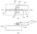
도 2는 본 발명의 바람직한 제1 실시예에 따른 데이터 통신 선로 구조를 도시한 개념도이다. 도 2에서, (a)는 제1 실시예에 따른 데이터 통신 선로 구조에 대한 평면도이다. (b)는 제1 실시예에 따른 데이터 통신 선로 구조에 대한 단면도로서, (a)에서 A-A' 부분을 절단하였을 때의 단면도이다(A-A' section view). (c)는 (b)에 도시된 제2 레이어(212)의 윗면과 바닥면을 도시한 도면이다. 이하 설명은 도 2를 참조한다.2 is a conceptual diagram illustrating a data communication line structure according to a first preferred embodiment of the present invention. 2 (a) is a plan view of the data communication line structure according to the first embodiment. (b) is a cross-sectional view of the data communication line structure according to the first embodiment, taken along line A-A 'in (a) (A-A' section view). (c) is a view showing an upper surface and a bottom surface of the
본 실시예에 따른 데이터 통신 선로 구조는 제1 기판층(200)과 제2 기판층(210)을 포함한다. 제2 기판층(210)은 적어도 일부분이 제1 기판층(200) 위에 적층되는 것으로서, 제1 레이어(211)와 제2 레이어(212)를 포함한다.The data communication line structure according to this embodiment includes a
제1 기판층(200)은 일면에 데이터 전송 선로가 형성된 것이다. 제1 기판층(200)은 메인 보드(mainboard) 기능을 하는 것으로서, 광통신 소자를 구동시키기 위한 주요 부품, 예컨대 중앙처리장치(CPU)가 장착되는 인쇄회로기판(PCB)이다.The
제1 레이어(211)는 GND 기능을 하는 것이다. 제1 레이어(211)에는 일측에 그라운드 플레인(Ground plane)의 불연속면이 형성되어 있다. 제1 레이어(211)는 GND 기능 외에 제어/구동 관련 신호선도 형성될 수 있다.The
제2 레이어(212)는 제1 레이어(211) 위에 구비된 것으로서, 일면에 데이터 통신 패턴(240)과 GND 패턴(230)이 형성된다. 바람직하게는, 제2 레이어(212)는 제1 레이어(211)의 불연속면 위에 위치하는 데이터 통신 패턴(240)만 GND 패턴(230)에 평행하지 않게 형성된다. 상기에서, 데이터 통신 패턴(240)은 제1 기판층(200) 상의 데이터 전송 선로(201)에 접속되는 것이다. GND 패턴(230)은 데이터 통신 패턴(240)과 동일 면에 형성되는 것으로서 데이터 통신 패턴(240)에 평행하지 않은 것이다.The
제2 레이어(212)는 GND 패턴(230)의 적어도 일측으로부터 연장되어 데이터 통신 패턴(240) 쪽으로 돌출 형성된 제1 임피던스 매칭 패턴(250)을 통해 데이터 통신 패턴(240)이 GND 패턴(230)에 평행하지 않게 형성된다. 본 실시예에서 제1 임피던스 매칭 패턴(250)은 CPW(CoPlanar Waveguide) 구조를 적용하여 형성시킬 수 있다.The
제1 임피던스 매칭 패턴(250)은 일단이 타단보다 더 데이터 통신 패턴(240) 쪽으로 돌출 형성된다. 이때, 제1 임피던스 매칭 패턴(250)은 삼각형 형태, 예컨대 직각삼각형 형태로 구현될 수 있다. 예컨대, 제1 임피던스 매칭 패턴(250)에서 상기 일단을 제1 단이라 하고 상기 타단을 제2 단이라 할 때, GND 패턴(230)으로부터 데이터 통신 패턴(240)까지의 거리에 대비하여, 제1 단으로부터 데이터 통신 패턴(240)까지의 거리는 10% ~ 30%, 제2 단으로부터 데이터 통신 패턴(240)까지의 거리는 70% ~ 90%일 수 있다. 제1 임피던스 매칭 패턴(250)은 GND 패턴(230)의 끝에 위치한다.The first
제2 기판층은 플렉시블(flexible)한 PCB, 즉 FPCB로 구현될 수 있다. 이때, 제2 레이어(212)의 데이터 통신 패턴(240)은 그 내부에 형성된 적어도 하나의 비아홀을 통해 제1 기판층(200)에 형성된 데이터 전송 선로(201)에 접속될 수 있으며, 데이터 통신 패턴(240) 양측에 형성된 제2 레이어(212)의 GND 패턴(230)은 그 내부에 형성된 적어도 하나의 비아홀(243)을 통해 제1 레이어(211)에 접속될 수 있다.The second substrate layer may be implemented as a flexible PCB, i.e., FPCB. The
플렉시블 PCB와 메인 보드를 연결시킬 때에 데이터 신호선과 그라운드(GND) 사이의 쇼트(short) 방지를 위해 일반적으로 전송선 구조(마이크로스트립 구조)를 가지는 신호의 바닥 그라운드 면에 불연속면(260)이 생긴다. 이를 GND 플레인(Ground plane)의 불연속면(260)이라 한다. 불연속면(260)에 해당되는 데이터 신호선의 임피던스 매칭을 위해 도 2에서는 제1 실시예로써 CPW(Co-Planar Waveguide) 구조를 적용한다. 도 2에서 제안한 구조로 데이터 통신 선로를 구현할 경우, 전체 신호 경로 상에 마이크로스트립과 CPW 사이의 천이(transition) 매칭 구조를 가질 수가 있다.In order to prevent a short between the data signal line and the ground (GND) when connecting the flexible PCB and the main board, a
한편, 도 2의 (c)에서 도면부호 241은 데이터 신호선 패드를 의미한다. 데이터 신호선 패드(241)는 제1 기판층(200) 상의 데이터 통신 선로와 물리적으로 분리되어 있으며, 접합 때에 솔더링 등에 의해 연결된다. 도면부호 242는 모듈과 연결되는 부분을 의미한다. 본 실시예에서 모듈과의 연결은 홀에 의한 연결에 한정되지 않으며, 패턴 형성을 통한 연결 등 다양한 케이스가 가능하다.In FIG. 2C,
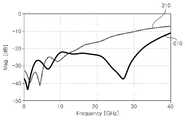
도 3은 종래 방법에 따른 반사값(310)과 본 발명의 제1 실시예에 따른 반사값(320)을 비교한 그래프이다. 이하 설명은 도 3을 참조한다.3 is a graph showing a comparison between the
본 발명의 제1 실시예에 따른 반사값(320)은 30GHz 이상의 주파수 영역에서도 10dB 이하의 양호한 반사값을 보이고 있다. 플렉시블 PCB 신호선 상에서 메인 보드와 연결되는 부분의 신호선 패드로의 연결 형태는 테퍼드(tapered) 형태를 가진다. 이 연결 형태는 테퍼드 형태 이외에 계단 형태(staircase)로도 구현 가능하다. 이러한 연결 형태는 신호선 패드와 윗면 그라운드와의 적당한 거리를 가지고 CPW 구조를 가능하게 한다. CPW 적용 구조는 바닥 그라운드의 불연속 부분에 해당되는 신호선의 임피던스 불연속을 해결하기 위한 구도이다. 플렉시블 PCB의 모듈과 연결되는 부분은 모듈의 구조에 따라 도 2의 (b)에 도시된 바와 같이 관통홀을 이용해 연결되거나 신호선 상의 패턴을 형성하여 연결하는 것도 가능하다. 이 부분에 있어서는 상기 방법 이외에 여러가지 형태의 연결 형태를 가질 수 있다. 계산시 사용한 플렉시블 PCB의 길이와 메인 보드(RO4350)의 길이는 TOSA 및 ROSA에서 사용 가능하도록 각각 12mm와 15mm로 했을 경우에 대한 결과이다.The
도 4와 도 5는 본 발명의 바람직한 제2 실시예에 따른 데이터 통신 선로 구조를 도시한 개념도이다. 도 4에서, (a)는 제2 실시예에 따른 데이터 통신 선로 구조에 대한 평면도이다. (b)는 제2 실시예에 따른 데이터 통신 선로 구조에 대한 단면도로서, (a)에서 A-A' 부분을 절단하였을 때의 단면도이다(A-A' section view). 도 5는 도 4의 (b)에 도시된 제2 레이어(212)의 윗면과 바닥면을 도시한 도면이다. 이하 설명은 도 4와 도 5를 참조한다.4 and 5 are conceptual diagrams showing a data communication line structure according to a second preferred embodiment of the present invention. 4 (a) is a plan view of the data communication line structure according to the second embodiment. (b) is a cross-sectional view of the data communication line structure according to the second embodiment, taken along line AA 'in (a) (AA' section view). FIG. 5 is a view showing an upper surface and a bottom surface of the
제2 레이어(212)에는 데이터 통신 패턴(240)의 적어도 일측으로부터 연장되어 GND 패턴(230) 쪽으로 돌출 형성된 제2 임피던스 매칭 패턴(410)을 통해 데이터 통신 패턴(240)이 GND 패턴(230)에 평행하지 않게 형성된다. 제2 임피던스 매칭 패턴(410)은 오픈 스터브(open stub) 형태로 구현할 수 있다. 예컨대, 도 5의 도면부호 520과 같이 싱글 오픈 스터브(single open stub) 형태로 구현하거나 도 5의 도면부호 510과 같이 십자형 오픈 스터브 형태로 구현할 수 있다.The
제2 임피던스 매칭 패턴(410)은 일단과 타단이 동일하게 GND 패턴(230) 쪽으로 돌출 형성된다. 본 실시예에서 제2 임피던스 매칭 패턴(410)은 사각형 형태(ex. 직사각형 형태) 또는 원뿔 형태로 구현될 수 있다. 제2 임피던스 매칭 패턴(410)은 GND 패턴(230)과 마주하지 않는 측에 형성된다.The second
제2 임피던스 매칭 패턴(410)이 데이터 통신 패턴(240)의 일측에 형성될 때, 제2 임피던스 매칭 패턴(410)의 폭보다 제2 임피던스 매칭 패턴(410)의 길이를 더 큰 값으로 설정한다. 예컨대, 제2 임피던스 매칭 패턴(410)이 데이터 통신 패턴(240)의 일측에만 형성된 경우, 제2 임피던스 매칭 패턴(410)에서 상기 일단을 제1 단이라 하고 상기 타단을 제2 단이라 할 때, 데이터 통신 패턴(240)의 폭(W2)에 대비하여, GND 패턴(230)의 단부에 접하는 수직선과 만나는 점으로부터 제2 임피던스 매칭 패턴(410)까지의 거리(D)는 130% ~ 160%, 제2 임피던스 매칭 패턴(410)의 길이(H)는 140% ~ 170%, 제2 임피던스 매칭 패턴(410)의 폭(W1)은 90% ~ 110%일 수 있다.The length of the second
제2 임피던스 매칭 패턴(410)이 데이터 통신 패턴(240)의 양측에 형성될 때, 제2 임피던스 매칭 패턴(410)의 길이보다 제2 임피던스 매칭 패턴(410)의 폭을 더 큰 값으로 설정한다. 예컨대, 제2 임피던스 매칭 패턴(410)이 데이터 통신 패턴(240)의 양측 모두에 형성된 경우, 제2 임피던스 매칭 패턴(410)에서 상기 일단을 제1 단이라 하고 상기 타단을 제2 단이라 할 때, 데이터 통신 패턴(240)의 폭(W2)에 대비하여, GND 패턴(230)의 단부에 접하는 수직선과 만나는 점으로부터 제2 임피던스 매칭 패턴(410)까지의 거리(D)는 120% ~ 150%, 제2 임피던스 매칭 패턴(410)의 길이(H)는 90% ~ 110%, 제2 임피던스 매칭 패턴(410)의 폭(W1)은 140% ~ 170%일 수 있다.The width of the second
도 6은 종래 방법에 따른 반사값(310)과 본 발명의 제2 실시예에 따른 반사값(610)을 비교한 그래프이다. 이하 설명은 도 4 내지 도 6을 참조한다.6 is a graph showing a comparison between the
플렉시블 PCB와 메인 보드 간에 연결시킬 때에 데이터 신호선과 그라운드 사이의 쇼트(short) 방지를 위해 일반적으로 전송선 구조(마이크로스트립 구조)를 가지는 신호의 바닥 그라운드 면에 불연속면(260)이 생긴다. 또한, 데이터 통신 패턴(240)이 전송선 구조(마이크로스트립 구조)에서 데이터 신호선 패드(241)로 급격하게 선폭이 증가하며 제1 기판층과 제2 기판층을 연결시키기 위한 비아 홀에 의한 임피던스 연속점이 생긴다. 이와 같이 임피던스 불연속 부분에 해당하는 데이터 신호선의 임피던스 매칭을 위해 본 발명의 제2 실시예에서는 오픈 스터브(open stub) 기법을 적용한다. 불연속면에 해당되는 신호선의 인덕턴스(inductance) 성분(L1)과 메인 보드와 연결하기 위한 신호선 패드의 비아 홀(via hole)에 해당되는 인덕턴스 성분(L2)을 플렉시블 PCB 상에 마이크로스트립 오픈 스터브를 이용하여 원하는 주파수 대역에서의 공진을 시킴으로써 반사값을 크게 향상 시킬 수 있다.In order to prevent a short between the data signal line and the ground when connecting the flexible PCB to the main board, a
오픈 스터브는 도 5에 도시된 바와 같이 싱글 오픈 스터브(single open stub) 형태와 십자형 오픈 스터브의 형태로 구현할 수 있다. 플렉시블 PCB의 모듈과 연결되는 부분은 모듈 구조에 따라 관통홀을 이용해 연결되거나 신호선 상의 패턴을 형성하여 연결할 수도 있다. 이 부분에 있어서는 상기 방법 이외에 여러가지 형태의 연결 형태를 가질 수 있다.The open stub can be implemented in the form of a single open stub and a cross open stub as shown in FIG. Depending on the module structure, the part of the flexible PCB connected to the module may be connected by using a through hole or by forming a pattern on a signal line. In this part, there are various types of connection forms other than the above-mentioned method.
도 5는 플렉시블 PCB 길이가 12mm이고 메인 보드(RO4350)의 길이가 15mm일 때, 계산된 반사값을 보여주고 있다. 각각 오픈 스터브의 규격(W1, W2, H, D)에 따라 원하는 주파수에서 공진을 일으켜 반사값을 크게 향상시킬 수 있다. 여기서 D는 바닥면 그라운드 불연속 영역에 해당되는 윗면의 신호선 길이이다. 계산시 사용한 플렉시블 PCB의 길이와 메인 보드(RO4350)의 길이는 TOSA 및 ROSA에서 사용 가능하도록 각각 12mm와 15mm로 했을 경우에 대한 결과이다.FIG. 5 shows calculated reflection values when the length of the flexible PCB is 12 mm and the length of the main board (RO 4350) is 15 mm. Resonance occurs at a desired frequency according to the specifications (W1, W2, H, D) of the open stub, respectively, so that the reflection value can be greatly improved. Where D is the signal line length of the top surface corresponding to the bottom surface discontinuity region. The length of the flexible PCB used in the calculation and the length of the main board (RO4350) are the results for 12mm and 15mm for TOSA and ROSA, respectively.
다음으로, 인쇄회로기판(PCB)을 이용하여 데이터 통신 선로를 설계하는 방법을 설명한다. 도 7은 본 발명의 바람직한 실시예에 따른 데이터 통신 선로 설계 방법을 도시한 흐름도이다. 이하 설명은 도 7을 참조한다.Next, a method of designing a data communication line using a printed circuit board (PCB) will be described. 7 is a flowchart illustrating a data communication line design method according to a preferred embodiment of the present invention. The following description refers to Fig.
먼저, 제1 기판층의 일면에 데이터 전송 선로를 형성시킨다(선로 형성 단계, S700).First, a data transmission line is formed on one surface of the first substrate layer (line forming step, S700).
선로 형성 단계(S700) 이후, GND 기능을 하는 제1 레이어를 밑면으로 하는 제2 기판층의 적어도 일부분을 제1 기판층 위에 적층시킨다(적층 단계, S710). 적층 단계(S710)에서는 제1 레이어의 일측에 그라운드 플레인(Ground plane)의 불연속면을 형성시킬 수 있다.After the line forming step S700, at least a part of the second substrate layer having the GND functioning as the first layer is laminated on the first substrate layer (laminating step, S710). In the stacking step S710, a discontinuity surface of a ground plane may be formed on one side of the first layer.
적층 단계(S710) 이후, 제2 기판층에 포함되는 것으로서 제1 레이어 위에 위치하는 제2 레이어의 일면에 데이터 전송 선로에 접속되는 데이터 통신 패턴과 데이터 통신 패턴에 평행하지 않은 GND 패턴을 형성시킨다(패턴 형성 단계, S720). 바람직하게는, 패턴 형성 단계(S720)에서는 제1 레이어의 불연속면 위에 위치하는 데이터 통신 패턴만 GND 패턴에 평행하지 않게 형성시킨다.After the stacking step S710, a data communication pattern connected to the data transmission line and a GND pattern not parallel to the data communication pattern are formed on one surface of the second layer, which is included in the second substrate layer and is located on the first layer Pattern formation step, S720). Preferably, in the pattern forming step S720, only the data communication pattern located on the discontinuity surface of the first layer is formed so as not to be parallel to the GND pattern.
데이터 통신 패턴이 GND 패턴에 평행하지 않게 형성시킬 때에, 제1 타입으로 패턴 형성 단계(S720)에서는 GND 패턴의 적어도 일측으로부터 연장되는 제1 임피던스 매칭 패턴을 데이터 통신 패턴 쪽으로 돌출 형성시킨다. 이때, 제1 임피던스 매칭 패턴의 일단을 제1 임피던스 매칭 패턴의 타단보다 더 데이터 통신 패턴 쪽으로 돌출 형성시킨다. 제1 임피던스 매칭 패턴은 GND 패턴의 끝에 형성된다.When forming the data communication pattern not parallel to the GND pattern, a first impedance matching pattern extending from at least one side of the GND pattern is protruded toward the data communication pattern in the first type pattern formation step (S720). At this time, one end of the first impedance matching pattern is protruded toward the data communication pattern than the other end of the first impedance matching pattern. The first impedance matching pattern is formed at the end of the GND pattern.
데이터 통신 패턴이 GND 패턴에 평행하지 않게 형성시킬 때에, 제2 타입으로 패턴 형성 단계(S720)에서는 데이터 통신 패턴의 적어도 일측으로부터 연장되는 제2 임피던스 매칭 패턴을 GND 패턴 쪽으로 돌출 형성시켜 데이터 통신 패턴이 GND 패턴에 평행하지 않게 형성시킨다. 이때, 제2 임피던스 매칭 패턴의 일단과 제2 임피던스 매칭 패턴의 타단을 동일하게 GND 패턴 쪽으로 돌출 형성시킨다. 제2 임피던스 매칭 패턴은 GND 패턴과 마주하지 않는 측에 형성된다.The second impedance matching pattern extending from at least one side of the data communication pattern is protruded toward the GND pattern in the pattern formation step S720 of the second type when the data communication pattern is formed not parallel to the GND pattern, It is formed so as not to be parallel to the GND pattern. At this time, one end of the second impedance matching pattern and the other end of the second impedance matching pattern protrude toward the GND pattern. The second impedance matching pattern is formed on the side not facing the GND pattern.
제2 임피던스 매칭 패턴을 데이터 통신 패턴의 일측에 형성시킬 때, 제2 임피던스 매칭 패턴의 폭보다 제2 임피던스 매칭 패턴의 길이를 더 큰 값으로 설정한다. 반면, 제2 임피던스 매칭 패턴을 데이터 통신 패턴의 양측에 형성시킬 때, 제2 임피던스 매칭 패턴의 길이보다 제2 임피던스 매칭 패턴의 폭을 더 큰 값으로 설정한다.When the second impedance matching pattern is formed on one side of the data communication pattern, the length of the second impedance matching pattern is set to a larger value than the width of the second impedance matching pattern. On the other hand, when the second impedance matching pattern is formed on both sides of the data communication pattern, the width of the second impedance matching pattern is set to a larger value than the length of the second impedance matching pattern.
한편, 패턴 형성 단계(S720)에서는 제2 기판층으로 플렉시블(flexible)한 인쇄회로기판(PCB), 즉 FPCB를 이용할 수 있다. 패턴 형성 단계(S720)에서는 제2 레이어의 데이터 통신 패턴을 그 내부에 형성된 적어도 하나의 비아홀을 통해 제1 기판층에 형성된 데이터 전송 선로에 접속시키며, 데이터 통신 패턴 양측에 형성된 제2 레이어의 GND 패턴은 그 내부에 형성된 적어도 하나의 비아홀을 통해 제1 레이어에 접속시킬 수 있다.Meanwhile, in the pattern formation step S720, a flexible printed circuit board (PCB), i.e., FPCB, may be used for the second substrate layer. In the pattern formation step S720, the data communication pattern of the second layer is connected to the data transmission line formed in the first substrate layer through at least one via hole formed therein, and the GND pattern of the second layer formed on both sides of the data communication pattern May be connected to the first layer through at least one via hole formed therein.
이상의 설명은 본 발명의 기술 사상을 예시적으로 설명한 것에 불과한 것으로서, 본 발명이 속하는 기술 분야에서 통상의 지식을 가진 자라면 본 발명의 본질적인 특성에서 벗어나지 않는 범위 내에서 다양한 수정, 변경 및 치환이 가능할 것이다. 따라서, 본 발명에 개시된 실시예 및 첨부된 도면들은 본 발명의 기술 사상을 한정하기 위한 것이 아니라 설명하기 위한 것이고, 이러한 실시예 및 첨부된 도면에 의하여 본 발명의 기술 사상의 범위가 한정되는 것은 아니다. 본 발명의 보호 범위는 아래의 청구 범위에 의하여 해석되어야 하며, 그와 동등한 범위 내에 있는 모든 기술 사상은 본 발명의 권리 범위에 포함되는 것으로 해석되어야 할 것이다.It will be apparent to those skilled in the art that various modifications, substitutions and substitutions are possible, without departing from the scope and spirit of the invention as disclosed in the accompanying claims. will be. Therefore, the embodiments disclosed in the present invention and the accompanying drawings are intended to illustrate and not to limit the technical spirit of the present invention, and the scope of the technical idea of the present invention is not limited by these embodiments and the accompanying drawings . The scope of protection of the present invention should be construed according to the following claims, and all technical ideas within the scope of equivalents should be construed as falling within the scope of the present invention.
본 발명은 고속 광통신 소자의 전기적 연결을 위한 플렉시블 PCB 상에서의 데이터 신호선의 구조와 관련된 것이다. 본 발명은 이더넷 분야, TDM 분야, WDM 분야 등에 적용될 수 있다.The present invention relates to a structure of a data signal line on a flexible PCB for electrical connection of a high-speed optical communication device. The present invention can be applied to the Ethernet field, the TDM field, the WDM field, and the like.
200 : 제1 기판층 201 : 데이터 전송 선로
210 : 제2 기판층 211 : 제1 레이어
212 : 제2 레이어 230 : GND 패턴
240 : 데이터 통신 패턴 250 : 제1 임피던스 매칭 패턴
410 : 제2 임피던스 매칭 패턴200: first substrate layer 201: data transmission line
210: second substrate layer 211: first layer
212: second layer 230: GND pattern
240: data communication pattern 250: first impedance matching pattern
410: second impedance matching pattern
Claims (15)
Translated fromKorean적어도 일부분이 상기 제1 기판층 위에 적층되는 것으로서, GND 기능을 하는 제1 레이어, 및 상기 제1 레이어 위에 구비되는 것으로서 일면에 상기 데이터 전송 선로에 접속되는 데이터 통신 패턴과 상기 데이터 통신 패턴에 평행하지 않은 GND 패턴이 형성된 제2 레이어를 포함하는 제2 기판층
을 포함하는 것을 특징으로 하고,
상기 제1 레이어는 일측에 불연속면이 형성되며,
상기 제2 레이어는 상기 불연속면 위에 위치하는 상기 데이터 통신 패턴만 상기 GND 패턴에 평행하지 않게 형성된 것을 특징으로 하는 데이터 통신 선로 구조.A first substrate layer having a data transmission line formed on one surface thereof; And
At least a portion of which is stacked on the first substrate layer, the first layer having a GND function and a data communication pattern provided on the first layer, the data communication pattern being connected to the data transmission line, A second substrate layer including a second layer on which a non-GND pattern is formed
, Wherein:
Wherein the first layer has a discontinuous surface on one side,
And the second layer is formed such that only the data communication pattern located on the discontinuity surface is not parallel to the GND pattern.
상기 제2 레이어는 상기 GND 패턴의 적어도 일측으로부터 연장되어 상기 데이터 통신 패턴 쪽으로 돌출 형성된 제1 임피던스 매칭 패턴을 통해 상기 데이터 통신 패턴이 상기 GND 패턴에 평행하지 않게 형성되거나, 상기 데이터 통신 패턴의 적어도 일측으로부터 연장되어 상기 GND 패턴 쪽으로 돌출 형성된 제2 임피던스 매칭 패턴을 통해 상기 데이터 통신 패턴이 상기 GND 패턴에 평행하지 않게 형성된 것을 특징으로 하는 데이터 통신 선로 구조.The method according to claim 1,
Wherein the second layer is formed so that the data communication pattern is not parallel to the GND pattern through a first impedance matching pattern protruding from at least one side of the GND pattern and protruding toward the data communication pattern, Wherein the data communication pattern is formed so as not to be parallel to the GND pattern through a second impedance matching pattern protruding from the GND pattern.
상기 제1 임피던스 매칭 패턴은 일단이 타단보다 더 상기 데이터 통신 패턴 쪽으로 돌출 형성되는 것을 특징으로 하는 데이터 통신 선로 구조.The method of claim 3,
Wherein the first impedance matching pattern has one end protruded toward the data communication pattern than the other end.
상기 제1 임피던스 매칭 패턴은 상기 GND 패턴의 끝에 위치하는 것을 특징으로 하는 데이터 통신 선로 구조.5. The method of claim 4,
Wherein the first impedance matching pattern is located at the end of the GND pattern.
상기 제2 임피던스 매칭 패턴은 일단과 타단이 동일하게 상기 GND 패턴 쪽으로 돌출 형성되는 것을 특징으로 하는 데이터 통신 선로 구조.The method of claim 3,
Wherein the second impedance matching pattern is protruded toward the GND pattern at one end and the other end.
상기 제2 임피던스 매칭 패턴이 상기 데이터 통신 패턴의 일측에 형성될 때, 상기 제2 임피던스 매칭 패턴의 폭보다 상기 제2 임피던스 매칭 패턴의 길이를 더 큰 값으로 설정하며,
상기 제2 임피던스 매칭 패턴이 상기 데이터 통신 패턴의 양측에 형성될 때, 상기 제2 임피던스 매칭 패턴의 길이보다 상기 제2 임피던스 매칭 패턴의 폭을 더 큰 값으로 설정하는 것을 특징으로 하는 데이터 통신 선로 구조.The method according to claim 6,
The length of the second impedance matching pattern is set to a larger value than the width of the second impedance matching pattern when the second impedance matching pattern is formed on one side of the data communication pattern,
And the width of the second impedance matching pattern is set to a larger value than the length of the second impedance matching pattern when the second impedance matching pattern is formed on both sides of the data communication pattern. .
상기 제2 임피던스 매칭 패턴은 상기 GND 패턴과 마주하지 않는 측에 형성되는 것을 특징으로 하는 데이터 통신 선로 구조.The method of claim 3,
And the second impedance matching pattern is formed on a side not facing the GND pattern.
상기 제2 기판층은 플렉시블(flexible)한 것을 특징으로 하는 데이터 통신 선로 구조.The method according to claim 1,
And the second substrate layer is flexible.
GND 기능을 하는 제1 레이어를 밑면으로 하는 제2 기판층의 적어도 일부분을 상기 제1 기판층 위에 적층시키는 적층 단계; 및
상기 제2 기판층에 포함되는 것으로서 상기 제1 레이어 위에 위치하는 제2 레이어의 일면에 상기 데이터 전송 선로에 접속되는 데이터 통신 패턴과 상기 데이터 통신 패턴에 평행하지 않은 GND 패턴을 형성시키는 패턴 형성 단계
를 포함하는 것을 특징으로 하고,
상기 적층 단계에서는 상기 제1 레이어의 일측에 불연속면을 형성시키며,
상기 패턴 형성 단계에서는 상기 불연속면 위에 위치하는 상기 데이터 통신 패턴만 상기 GND 패턴에 평행하지 않게 형성시키는 것을 특징으로 하는 데이터 통신 선로 설계 방법.Forming a data transmission line on one surface of the first substrate layer;
A laminating step of laminating at least a part of a second substrate layer having a first layer as a bottom surface functioning as a GND on the first substrate layer; And
Forming a data communication pattern included in the second substrate layer and connected to the data transmission line and a GND pattern not parallel to the data communication pattern on one surface of the second layer positioned on the first layer,
, Wherein:
In the laminating step, a discontinuous surface is formed on one side of the first layer,
Wherein in the pattern formation step, only the data communication pattern located on the discontinuity surface is formed so as not to be parallel to the GND pattern.
상기 패턴 형성 단계에서는 상기 GND 패턴의 적어도 일측으로부터 연장되는 제1 임피던스 매칭 패턴을 상기 데이터 통신 패턴 쪽으로 돌출 형성시켜 상기 데이터 통신 패턴이 상기 GND 패턴에 평행하지 않게 형성시키거나, 상기 데이터 통신 패턴의 적어도 일측으로부터 연장되는 제2 임피던스 매칭 패턴을 상기 GND 패턴 쪽으로 돌출 형성시켜 상기 데이터 통신 패턴이 상기 GND 패턴에 평행하지 않게 형성시키는 것을 특징으로 하는 데이터 통신 선로 설계 방법.11. The method of claim 10,
In the pattern formation step, a first impedance matching pattern extending from at least one side of the GND pattern is protruded toward the data communication pattern to form the data communication pattern so as not to be parallel to the GND pattern, And a second impedance matching pattern extending from one side is protruded toward the GND pattern to form the data communication pattern so as not to be parallel to the GND pattern.
상기 패턴 형성 단계에서는 상기 제1 임피던스 매칭 패턴의 일단을 상기 제1 임피던스 매칭 패턴의 타단보다 더 상기 데이터 통신 패턴 쪽으로 돌출 형성시키는 것을 특징으로 하는 데이터 통신 선로 설계 방법.13. The method of claim 12,
Wherein the pattern forming step protrudes one end of the first impedance matching pattern toward the data communication pattern more than the other end of the first impedance matching pattern.
상기 패턴 형성 단계에서는 상기 제2 임피던스 매칭 패턴의 일단과 상기 제2 임피던스 매칭 패턴의 타단을 동일하게 상기 GND 패턴 쪽으로 돌출 형성시키는 것을 특징으로 하는 데이터 통신 선로 설계 방법.13. The method of claim 12,
Wherein the pattern forming step protrudes one end of the second impedance matching pattern and the other end of the second impedance matching pattern toward the GND pattern in the same manner.
상기 패턴 형성 단계에서는 상기 제2 임피던스 매칭 패턴을 상기 데이터 통신 패턴의 일측에 형성시킬 때 상기 제2 임피던스 매칭 패턴의 폭보다 상기 제2 임피던스 매칭 패턴의 길이를 더 큰 값으로 설정하며, 상기 제2 임피던스 매칭 패턴을 상기 데이터 통신 패턴의 양측에 형성시킬 때 상기 제2 임피던스 매칭 패턴의 길이보다 상기 제2 임피던스 매칭 패턴의 폭을 더 큰 값으로 설정하는 것을 특징으로 하는 데이터 통신 선로 설계 방법.15. The method of claim 14,
Wherein the pattern forming step sets the length of the second impedance matching pattern to a larger value than the width of the second impedance matching pattern when the second impedance matching pattern is formed on one side of the data communication pattern, Wherein the width of the second impedance matching pattern is set to a larger value than the length of the second impedance matching pattern when the impedance matching pattern is formed on both sides of the data communication pattern.
Priority Applications (2)
| Application Number | Priority Date | Filing Date | Title |
|---|---|---|---|
| KR1020110022970AKR101786083B1 (en) | 2011-03-15 | 2011-03-15 | Structure of transmission line for data communication, and method for designing of the said line |
| US13/365,491US20120235764A1 (en) | 2011-03-15 | 2012-02-03 | Structure of transmission line for data communication and method for designing the same |
Applications Claiming Priority (1)
| Application Number | Priority Date | Filing Date | Title |
|---|---|---|---|
| KR1020110022970AKR101786083B1 (en) | 2011-03-15 | 2011-03-15 | Structure of transmission line for data communication, and method for designing of the said line |
Publications (2)
| Publication Number | Publication Date |
|---|---|
| KR20120105264A KR20120105264A (en) | 2012-09-25 |
| KR101786083B1true KR101786083B1 (en) | 2017-10-17 |
Family
ID=46827987
Family Applications (1)
| Application Number | Title | Priority Date | Filing Date |
|---|---|---|---|
| KR1020110022970AExpired - Fee RelatedKR101786083B1 (en) | 2011-03-15 | 2011-03-15 | Structure of transmission line for data communication, and method for designing of the said line |
Country Status (2)
| Country | Link |
|---|---|
| US (1) | US20120235764A1 (en) |
| KR (1) | KR101786083B1 (en) |
Families Citing this family (18)
| Publication number | Priority date | Publication date | Assignee | Title |
|---|---|---|---|---|
| JP5348259B2 (en)* | 2012-02-02 | 2013-11-20 | 横河電機株式会社 | Insulation circuit and communication equipment |
| WO2014069061A1 (en)* | 2012-10-31 | 2014-05-08 | 株式会社村田製作所 | High-frequency signal line and manufacturing method therefor |
| KR20150095092A (en) | 2014-02-12 | 2015-08-20 | 한국전자통신연구원 | Board assembly for transmitting high speed signal and method of manufacturing the same |
| KR20150095094A (en) | 2014-02-12 | 2015-08-20 | 한국전자통신연구원 | Interface for transmitting high speed signal and optical module comprising the same |
| JP2015172683A (en)* | 2014-03-12 | 2015-10-01 | 富士通オプティカルコンポーネンツ株式会社 | Optical module |
| CN104836619B (en) | 2015-03-30 | 2017-08-29 | 青岛海信宽带多媒体技术有限公司 | A kind of optical device |
| CN104767103B (en) | 2015-03-30 | 2017-12-19 | 青岛海信宽带多媒体技术有限公司 | Connecting structure for laser and laser component |
| JP6437886B2 (en)* | 2015-06-16 | 2018-12-12 | 日本電信電話株式会社 | High frequency connection line |
| CN107072032B (en)* | 2017-02-15 | 2019-12-13 | 大连藏龙光电子科技有限公司 | A flexible printed circuit board structure |
| JP7078313B2 (en)* | 2018-03-07 | 2022-05-31 | 住友電工デバイス・イノベーション株式会社 | Semiconductor device |
| WO2019172332A1 (en) | 2018-03-07 | 2019-09-12 | Sumitomo Electric Device Innovations, Inc. | Semiconductor device |
| KR102730165B1 (en)* | 2019-07-26 | 2024-11-15 | 삼성전자 주식회사 | Electronic device including flexible printed circuit board |
| CN110933836B (en)* | 2019-11-20 | 2021-08-13 | 武汉光谷信息光电子创新中心有限公司 | Flexible circuit board, printed circuit board, rigid-flex board and manufacturing method thereof |
| KR102836343B1 (en)* | 2020-12-04 | 2025-07-21 | 엘에스머트리얼즈 주식회사 | The pcb for a capacitor and the manufacturing method of a capacitor module |
| US20220329029A1 (en)* | 2021-04-12 | 2022-10-13 | St. Jude Medical, Cardiology Division, Inc. | Method for bonding flexible electronic circuit elements |
| CN115811826A (en)* | 2021-09-13 | 2023-03-17 | 华为技术有限公司 | A kind of multilayer circuit board, circuit board assembly and electronic equipment |
| CN116666933A (en)* | 2022-02-18 | 2023-08-29 | 北京小米移动软件有限公司 | Electronic equipment and its radio frequency transmission lines |
| CN116072178B (en)* | 2023-01-29 | 2025-08-22 | 长鑫存储技术有限公司 | Layout structure and method of data sampling circuit |
Citations (2)
| Publication number | Priority date | Publication date | Assignee | Title |
|---|---|---|---|---|
| JP2001094012A (en) | 1999-09-22 | 2001-04-06 | Toyota Central Res & Dev Lab Inc | Semiconductor chip mounting substrate and high frequency device |
| JP2001144511A (en)* | 1999-11-17 | 2001-05-25 | Mitsubishi Electric Corp | Converter for connecting planar waveguides |
Family Cites Families (2)
| Publication number | Priority date | Publication date | Assignee | Title |
|---|---|---|---|---|
| JP2001308547A (en)* | 2000-04-27 | 2001-11-02 | Sharp Corp | High frequency multilayer circuit board |
| US8558637B2 (en)* | 2010-05-12 | 2013-10-15 | Mediatek Inc. | Circuit device with signal line transition element |
- 2011
- 2011-03-15KRKR1020110022970Apatent/KR101786083B1/ennot_activeExpired - Fee Related
- 2012
- 2012-02-03USUS13/365,491patent/US20120235764A1/ennot_activeAbandoned
Patent Citations (2)
| Publication number | Priority date | Publication date | Assignee | Title |
|---|---|---|---|---|
| JP2001094012A (en) | 1999-09-22 | 2001-04-06 | Toyota Central Res & Dev Lab Inc | Semiconductor chip mounting substrate and high frequency device |
| JP2001144511A (en)* | 1999-11-17 | 2001-05-25 | Mitsubishi Electric Corp | Converter for connecting planar waveguides |
Non-Patent Citations (1)
| Title |
|---|
| Toshitsugu Uesugi외 5인, "25 Gbps EML TOSA employing novel impedance-matched FPC design", ECOC, Vienna, Austria, 2009년 9월. |
Also Published As
| Publication number | Publication date |
|---|---|
| US20120235764A1 (en) | 2012-09-20 |
| KR20120105264A (en) | 2012-09-25 |
Similar Documents
| Publication | Publication Date | Title |
|---|---|---|
| KR101786083B1 (en) | Structure of transmission line for data communication, and method for designing of the said line | |
| EP2979321B1 (en) | A transition between a siw and a waveguide interface | |
| CN107371321B (en) | Printed circuit boards and optical modules | |
| US10687415B2 (en) | Flexible printed circuit board | |
| US9252474B2 (en) | Coupling arrangement | |
| US7564695B2 (en) | Circuit connection structure and printed circuit board | |
| US8558645B2 (en) | Apparatus for improving transmission bandwidth | |
| KR20090092706A (en) | System for interconnecting two substrates each comprising at least one transmission line | |
| JP2006245291A (en) | Transmission line and wiring formation method | |
| EP2979323A1 (en) | A siw antenna arrangement | |
| US8125289B2 (en) | Transmission line pairs with enhanced coupling therebetween and negligible coupling to ground | |
| KR100844218B1 (en) | High-frequency transmission line device capable of common mode filtering | |
| KR102677048B1 (en) | Flexible printed circuit board | |
| JP5153771B2 (en) | Terminator | |
| KR102677047B1 (en) | Flexible printed circuit board | |
| CN206452600U (en) | A flexible printed circuit board structure | |
| JP2013172128A (en) | Flexible substrate and optical module including the same | |
| EP1585184B1 (en) | Direct current cut structure | |
| JP4852979B2 (en) | Flex-rigid board, optical transceiver module and optical transceiver | |
| US20090056984A1 (en) | Signal transmission structure and layout method for the same | |
| JP4381701B2 (en) | Connection structure between coaxial connector and multilayer board | |
| KR102174480B1 (en) | Asymmetric coupling line capable of reducing the noise of a bent line and method of forming the same | |
| TWI783791B (en) | Antenna module | |
| JP7330241B2 (en) | circuit board | |
| US20250203758A1 (en) | Optical Module |
Legal Events
| Date | Code | Title | Description |
|---|---|---|---|
| PA0109 | Patent application | St.27 status event code:A-0-1-A10-A12-nap-PA0109 | |
| PG1501 | Laying open of application | St.27 status event code:A-1-1-Q10-Q12-nap-PG1501 | |
| R17-X000 | Change to representative recorded | St.27 status event code:A-3-3-R10-R17-oth-X000 | |
| PN2301 | Change of applicant | St.27 status event code:A-3-3-R10-R13-asn-PN2301 St.27 status event code:A-3-3-R10-R11-asn-PN2301 | |
| PA0201 | Request for examination | St.27 status event code:A-1-2-D10-D11-exm-PA0201 | |
| R17-X000 | Change to representative recorded | St.27 status event code:A-3-3-R10-R17-oth-X000 | |
| E902 | Notification of reason for refusal | ||
| PE0902 | Notice of grounds for rejection | St.27 status event code:A-1-2-D10-D21-exm-PE0902 | |
| E13-X000 | Pre-grant limitation requested | St.27 status event code:A-2-3-E10-E13-lim-X000 | |
| P11-X000 | Amendment of application requested | St.27 status event code:A-2-2-P10-P11-nap-X000 | |
| P13-X000 | Application amended | St.27 status event code:A-2-2-P10-P13-nap-X000 | |
| E701 | Decision to grant or registration of patent right | ||
| PE0701 | Decision of registration | St.27 status event code:A-1-2-D10-D22-exm-PE0701 | |
| GRNT | Written decision to grant | ||
| PR0701 | Registration of establishment | St.27 status event code:A-2-4-F10-F11-exm-PR0701 | |
| PR1002 | Payment of registration fee | St.27 status event code:A-2-2-U10-U11-oth-PR1002 Fee payment year number:1 | |
| PG1601 | Publication of registration | St.27 status event code:A-4-4-Q10-Q13-nap-PG1601 | |
| PC1903 | Unpaid annual fee | St.27 status event code:A-4-4-U10-U13-oth-PC1903 Not in force date:20201011 Payment event data comment text:Termination Category : DEFAULT_OF_REGISTRATION_FEE | |
| PC1903 | Unpaid annual fee | St.27 status event code:N-4-6-H10-H13-oth-PC1903 Ip right cessation event data comment text:Termination Category : DEFAULT_OF_REGISTRATION_FEE Not in force date:20201011 |