KR101783352B1 - Flat panel display apparatus and manufacturing method of the same - Google Patents
Flat panel display apparatus and manufacturing method of the sameDownload PDFInfo
- Publication number
- KR101783352B1 KR101783352B1KR1020100057567AKR20100057567AKR101783352B1KR 101783352 B1KR101783352 B1KR 101783352B1KR 1020100057567 AKR1020100057567 AKR 1020100057567AKR 20100057567 AKR20100057567 AKR 20100057567AKR 101783352 B1KR101783352 B1KR 101783352B1
- Authority
- KR
- South Korea
- Prior art keywords
- electrode
- capacitor
- insulating film
- layer
- transparent conductive
- Prior art date
- Legal status (The legal status is an assumption and is not a legal conclusion. Google has not performed a legal analysis and makes no representation as to the accuracy of the status listed.)
- Active
Links
Images


Classifications
- G—PHYSICS
- G02—OPTICS
- G02F—OPTICAL DEVICES OR ARRANGEMENTS FOR THE CONTROL OF LIGHT BY MODIFICATION OF THE OPTICAL PROPERTIES OF THE MEDIA OF THE ELEMENTS INVOLVED THEREIN; NON-LINEAR OPTICS; FREQUENCY-CHANGING OF LIGHT; OPTICAL LOGIC ELEMENTS; OPTICAL ANALOGUE/DIGITAL CONVERTERS
- G02F1/00—Devices or arrangements for the control of the intensity, colour, phase, polarisation or direction of light arriving from an independent light source, e.g. switching, gating or modulating; Non-linear optics
- G02F1/01—Devices or arrangements for the control of the intensity, colour, phase, polarisation or direction of light arriving from an independent light source, e.g. switching, gating or modulating; Non-linear optics for the control of the intensity, phase, polarisation or colour
- G02F1/13—Devices or arrangements for the control of the intensity, colour, phase, polarisation or direction of light arriving from an independent light source, e.g. switching, gating or modulating; Non-linear optics for the control of the intensity, phase, polarisation or colour based on liquid crystals, e.g. single liquid crystal display cells
- G02F1/133—Constructional arrangements; Operation of liquid crystal cells; Circuit arrangements
- G02F1/136—Liquid crystal cells structurally associated with a semi-conducting layer or substrate, e.g. cells forming part of an integrated circuit
- G02F1/1362—Active matrix addressed cells
- G02F1/136213—Storage capacitors associated with the pixel electrode
- H—ELECTRICITY
- H10—SEMICONDUCTOR DEVICES; ELECTRIC SOLID-STATE DEVICES NOT OTHERWISE PROVIDED FOR
- H10D—INORGANIC ELECTRIC SEMICONDUCTOR DEVICES
- H10D30/00—Field-effect transistors [FET]
- H10D30/60—Insulated-gate field-effect transistors [IGFET]
- H10D30/67—Thin-film transistors [TFT]
- H10D30/6729—Thin-film transistors [TFT] characterised by the electrodes
- H10D30/6737—Thin-film transistors [TFT] characterised by the electrodes characterised by the electrode materials
- H10D30/6739—Conductor-insulator-semiconductor electrodes
- H—ELECTRICITY
- H10—SEMICONDUCTOR DEVICES; ELECTRIC SOLID-STATE DEVICES NOT OTHERWISE PROVIDED FOR
- H10D—INORGANIC ELECTRIC SEMICONDUCTOR DEVICES
- H10D86/00—Integrated devices formed in or on insulating or conducting substrates, e.g. formed in silicon-on-insulator [SOI] substrates or on stainless steel or glass substrates
- H10D86/40—Integrated devices formed in or on insulating or conducting substrates, e.g. formed in silicon-on-insulator [SOI] substrates or on stainless steel or glass substrates characterised by multiple TFTs
- H10D86/481—Integrated devices formed in or on insulating or conducting substrates, e.g. formed in silicon-on-insulator [SOI] substrates or on stainless steel or glass substrates characterised by multiple TFTs integrated with passive devices, e.g. auxiliary capacitors
- H—ELECTRICITY
- H10—SEMICONDUCTOR DEVICES; ELECTRIC SOLID-STATE DEVICES NOT OTHERWISE PROVIDED FOR
- H10D—INORGANIC ELECTRIC SEMICONDUCTOR DEVICES
- H10D86/00—Integrated devices formed in or on insulating or conducting substrates, e.g. formed in silicon-on-insulator [SOI] substrates or on stainless steel or glass substrates
- H10D86/40—Integrated devices formed in or on insulating or conducting substrates, e.g. formed in silicon-on-insulator [SOI] substrates or on stainless steel or glass substrates characterised by multiple TFTs
- H10D86/60—Integrated devices formed in or on insulating or conducting substrates, e.g. formed in silicon-on-insulator [SOI] substrates or on stainless steel or glass substrates characterised by multiple TFTs wherein the TFTs are in active matrices
- H—ELECTRICITY
- H10—SEMICONDUCTOR DEVICES; ELECTRIC SOLID-STATE DEVICES NOT OTHERWISE PROVIDED FOR
- H10K—ORGANIC ELECTRIC SOLID-STATE DEVICES
- H10K50/00—Organic light-emitting devices
- H10K50/80—Constructional details
- H10K50/805—Electrodes
- H10K50/82—Cathodes
- H10K50/828—Transparent cathodes, e.g. comprising thin metal layers
- H—ELECTRICITY
- H10—SEMICONDUCTOR DEVICES; ELECTRIC SOLID-STATE DEVICES NOT OTHERWISE PROVIDED FOR
- H10K—ORGANIC ELECTRIC SOLID-STATE DEVICES
- H10K59/00—Integrated devices, or assemblies of multiple devices, comprising at least one organic light-emitting element covered by group H10K50/00
- H10K59/10—OLED displays
- H10K59/12—Active-matrix OLED [AMOLED] displays
- H10K59/121—Active-matrix OLED [AMOLED] displays characterised by the geometry or disposition of pixel elements
- H10K59/1216—Active-matrix OLED [AMOLED] displays characterised by the geometry or disposition of pixel elements the pixel elements being capacitors
- H—ELECTRICITY
- H10—SEMICONDUCTOR DEVICES; ELECTRIC SOLID-STATE DEVICES NOT OTHERWISE PROVIDED FOR
- H10K—ORGANIC ELECTRIC SOLID-STATE DEVICES
- H10K59/00—Integrated devices, or assemblies of multiple devices, comprising at least one organic light-emitting element covered by group H10K50/00
- H10K59/10—OLED displays
- H10K59/12—Active-matrix OLED [AMOLED] displays
- H10K59/123—Connection of the pixel electrodes to the thin film transistors [TFT]
- G—PHYSICS
- G02—OPTICS
- G02F—OPTICAL DEVICES OR ARRANGEMENTS FOR THE CONTROL OF LIGHT BY MODIFICATION OF THE OPTICAL PROPERTIES OF THE MEDIA OF THE ELEMENTS INVOLVED THEREIN; NON-LINEAR OPTICS; FREQUENCY-CHANGING OF LIGHT; OPTICAL LOGIC ELEMENTS; OPTICAL ANALOGUE/DIGITAL CONVERTERS
- G02F2201/00—Constructional arrangements not provided for in groups G02F1/00 - G02F7/00
- G02F2201/40—Arrangements for improving the aperture ratio
Landscapes
- Physics & Mathematics (AREA)
- Engineering & Computer Science (AREA)
- Microelectronics & Electronic Packaging (AREA)
- Nonlinear Science (AREA)
- Optics & Photonics (AREA)
- Chemical & Material Sciences (AREA)
- Crystallography & Structural Chemistry (AREA)
- Mathematical Physics (AREA)
- General Physics & Mathematics (AREA)
- Power Engineering (AREA)
- Geometry (AREA)
- Liquid Crystal (AREA)
- Thin Film Transistor (AREA)
- Devices For Indicating Variable Information By Combining Individual Elements (AREA)
Abstract
Translated fromKoreanDescription
Translated fromKorean본 발명은 평판 표시 장치 및 그 제조 방법에 관한 것이다.The present invention relates to a flat panel display and a method of manufacturing the same.
유기 발광 표시 장치 및 액정 표시 장치 등을 포함하는 평판 표시 장치는 고해상도의 디스플레이를 구현하기 위해 각 픽셀마다 박막 트랜지스터와 커패시터가 포함된 능동 구동형으로 제작된다.In order to realize high resolution display, a flat panel display device including an organic light emitting display device and a liquid crystal display device is manufactured as an active driving type including a thin film transistor and a capacitor for each pixel.
백라이트에서 방출되는 빛을 액정 표시 장치의 외부로 투과시켜야 하는 투과형 또는 반투과형 액정 표시 장치나, 유기 발광층에서 방출되는 빛을 박막 트랜지스터 어레이 기판으로 투과시켜야 하는 배면 발광형 또는 양면 발광형 유기 발광 표시 장치의 경우, 표시 품질을 향상시키기 위해 박막 트랜지스터 어레이 기판의 투과율을 높일 필요가 있다. 특히, 고해상도의 표시 장치일수록 개구율이 급격히 감소하고, 개구율이 감소함에 따라 투과율도 감소하는 문제가 있다.A transmissive or semi-transmissive liquid crystal display device in which light emitted from a backlight must be transmitted to the outside of a liquid crystal display device, a backlight emission type or double-side emission type organic light emitting display device in which light emitted from the organic emission layer must be transmitted to a thin film transistor array substrate It is necessary to increase the transmittance of the thin film transistor array substrate in order to improve display quality. Particularly, there is a problem that the aperture ratio decreases sharply as the display device of high resolution decreases, and the transmittance also decreases as the aperture ratio decreases.
본 발명은 상기와 같은 문제 및 그 밖의 문제점을 해결하기 위하여, 개구율 및 투과율이 향상된 평판 표시 장치 및 그 제조 방법을 제공하는 것을 목적으로 한다.SUMMARY OF THE INVENTION It is an object of the present invention to provide a flat panel display with improved aperture ratio and transmittance and a method of manufacturing the same, in order to solve the above problems and other problems.
본 발명의 일 측면에 의하면, 평판 표시 장치는, 기판 위에 배치된 게이트 전극과, 제1 절연막을 사이에 두고 상기 게이트 전극 위에 배치되고, 투명 도전성 산화물을 포함하는 반도체층과, 상기 게이트 전극과 동일층에 배치된 커패시터 제1 전극, 및 상기 제1 절연막을 사이에 두고 상기 반도체층과 동일 재료로 형성되며, 상기 반도체층과 동일층에 배치된 커패시터 제2전극과, 제2 절연막을 사이에 두고 서로 이격되어 배치되고, 상기 반도체층 및 상기 커패시터 제2 전극과 연결된 소스 전극과 드레인 전극과, 상기 소스 전극 및 드레인 전극을 덮는 유기 절연막과, 상기 제3 절연막 위에 배치되고, 상기 소스 전극 및 드레인 전극 중 하나와 연결된 화소 전극을 포함할 수 있다.According to an aspect of the present invention, there is provided a flat panel display comprising: a gate electrode disposed on a substrate; a semiconductor layer disposed on the gate electrode with a first insulating film interposed therebetween, the semiconductor layer including a transparent conductive oxide; And a capacitor second electrode formed on the same layer as the semiconductor layer and made of the same material as the semiconductor layer with the first insulating film interposed therebetween and a capacitor second electrode formed on the same layer as the semiconductor layer, A source electrode and a drain electrode connected to the semiconductor layer and the capacitor second electrode, an organic insulating film covering the source electrode and the drain electrode, and a source electrode and a drain electrode disposed on the third insulating film, And a pixel electrode connected to one of the pixel electrodes.
본 발명에 있어서, 상기 게이트 전극은 투명 도전층, 및 상기 투명 도전층 위에 배치된 금속층을 포함할 수 있다.In the present invention, the gate electrode may include a transparent conductive layer and a metal layer disposed on the transparent conductive layer.
본 발명에 있어서, 상기 커패시터 제1 전극은 상기 게이트 전극의 투명 도전층과 동일 재료로 형성될 수 있다.In the present invention, the capacitor first electrode may be formed of the same material as the transparent conductive layer of the gate electrode.
본 발명에 있어서, 상기 투명 도전층 및 상기 금속층은 외측 식각면은 동일면 상에 위치할 수 있다.In the present invention, the transparent conductive layer and the metal layer may be located on the same side of the outer etched surface.
본 발명에 있어서, 상기 커패시터 제1 전극은 인듐틴옥사이드(indium tin oxide: ITO), 인듐징크옥사이드(indium zink oxide: IZO), 징크옥사이드(zink oxide: ZnO), 인듐옥사이드(indium oxide: In2O3), 인듐갈륨옥사이드(indium galium oxide: IGO), 및 알루미늄징크옥사이드(aluminium zink oxide: AZO)을 포함하는 그룹에서 선택된 적어도 하나를 포함할 수 있다.In the present invention, the capacitor first electrode may be formed of indium tin oxide (ITO), indium zinc oxide (IZO), zinc oxide (ZnO), indium oxide (In2O3) , Indium gallium oxide (IGO), and aluminum zink oxide (AZO).
본 발명에 있어서, 상기 투명 도전성 산화물은 갈륨(Ga), 인(In), 아연(Zn) 및 주석(Sn) 군에서 선택된 하나 이상의 원소, 및 산소(O)를 포함할 수 있다.In the present invention, the transparent conductive oxide may include at least one element selected from the group consisting of gallium (Ga), indium (In), zinc (Zn) and tin (Sn), and oxygen (O).
본 발명에 있어서, 상기 제1 절연막은 상기 제3 절연막보다 큰 유전율을 가질 수 있다.In the present invention, the first insulating film may have a larger dielectric constant than the third insulating film.
본 발명에 있어서, 상기 제1 절연막은 무기 절연물을 포함하고, 상기 제3 절연막은 유기 절연물을 포함할 수 있다.In the present invention, the first insulating film may include an inorganic insulating material, and the third insulating film may include an organic insulating material.
본 발명에 있어서, 상기 소스 전극 및 드레인 전극과 동일층에 상기 소스 전극 및 드레인 전극에 데이터 전압을 인가하는 데이터 배선이 구비될 수 있다.In the present invention, a data line for applying a data voltage to the source electrode and the drain electrode may be provided on the same layer as the source electrode and the drain electrode.
본 발명에 있어서, 상기 제3 절연막은 상기 제1 절연막보다 두꺼울 수 있다.In the present invention, the third insulating film may be thicker than the first insulating film.
본 발명에 있어서, 상기 커패시터 제2 전극 위의 상기 제2 절연막은 제거되고, 상기 커패시터 제2 전극은 상기 제3 절연막과 직접 접촉할 수 있다.In the present invention, the second insulating film on the capacitor second electrode may be removed, and the capacitor second electrode may directly contact the third insulating film.
본 발명에 있어서, 상기 커패시터 제2 전극과 상기 제3 절연막 사이에 배치되고, 상기 소스 전극 및 드레인 전극과 동일 재료로 형성된 커패시터 제3 전극을 더 구비할 수 있다.The capacitor may further include a capacitor third electrode disposed between the capacitor second electrode and the third insulating film and formed of the same material as the source electrode and the drain electrode.
본 발명에 있어서, 상기 제1 절연막 및 상기 제2 절연막은 동일한 절연물을 포함할 수 있다.In the present invention, the first insulating film and the second insulating film may include the same insulating material.
본 발명에 있어서, 상기 제1 절연막 및 상기 제2 절연막은 실리콘 옥사이드(silicon oxide:SiOx)를 포함할 수 있다.In the present invention, the first insulating layer and the second insulating layer may include silicon oxide (SiOx).
본 발명에 있어서, 상기 화소 전극은 상기 제3 절연막에 형성된 비아홀을 통하여 상기 커패시터 제2 전극 위에 직접 접촉할 수 있다.In the present invention, the pixel electrode may directly contact the capacitor second electrode through a via hole formed in the third insulating film.
본 발명에 있어서, 상기 화소 전극은 투명 전극일 수 있다.In the present invention, the pixel electrode may be a transparent electrode.
본 발명에 있어서, 상기 화소 전극에 대향하는 대향 전극을 더 포함하고, 상기 화소 전극과 상기 대향 전극 사이에 액정이 포함될 수 있다.The liquid crystal display according to the present invention may further include a counter electrode facing the pixel electrode, and liquid crystal may be included between the pixel electrode and the counter electrode.
본 발명에 있어서, 상기 커패시터 제1 전극에 Vcom, Vgh, 또는 Vgl이 인가될 수 있다.In the present invention, Vcom, Vgh, or Vgl may be applied to the capacitor first electrode.
본 발명에 있어서, 상기 화소 전극에 대향하는 대향 전극을 더 포함하고, 상기 화소 전극과 상기 대향 전극 사이에 유기 발광층이 포함될 수 있다.In the present invention, the organic light emitting device may further include a counter electrode facing the pixel electrode, and an organic light emitting layer may be included between the pixel electrode and the counter electrode.
본 발명의 다른 측면에 의하면, 평판 표시 장치의 제조 방법은, 기판 위에 박막 트랜지스터의 게이트 전극 및 커패시터 제1 전극을 형성하는 제1 마스크 공정과, 제1 절연막을 사이에 두고, 상기 박막 트랜지스터의 반도체층 및 커패시터 제2 전극을 형성하는 제2 마스크 공정과, 제2 절연막을 형성하고, 상기 제2 절연막을 관통하여 상기 반도체층의 일부 및 커패시터 제2 전극의 일부를 노출시키는 콘택홀을 형성하는 제3 마스크 공정과, 상기 콘택홀을 통해 상기 반도체층 및 커패시터 제2 전극과 연결된 소스 전극 및 드레인 전극을 형성하는 제4 마스크 공정과, 제3 절연막을 형성하고, 비아홀을 형성하는 제5 마스크 공정과, 상기 비아홀을 통하여 상기 소스 전극 및 드레인 전극 중 하나에 연결되는 화소 전극을 형성하는 제6 마스크 공정을 포함할 수 있다.According to another aspect of the present invention, there is provided a method of manufacturing a flat panel display including a first mask process for forming a gate electrode and a capacitor first electrode of a thin film transistor on a substrate, And forming a second contact hole for exposing a part of the semiconductor layer and a part of the capacitor second electrode through the second insulating film, A fourth mask process for forming source and drain electrodes connected to the semiconductor layer and the capacitor second electrode through the contact hole, a fifth mask process for forming a third insulating film and forming a via hole, And a sixth mask process for forming a pixel electrode connected to one of the source electrode and the drain electrode through the via hole.
본 발명에 있어서, 상기 제1 마스크 공정에서, 상기 게이트 전극은 투명 도전층 및 상기 투명 도전층 위에 배치된 금속층을 포함하고, 상기 커패시터 제1전극은 상기 투명 도전층과 동일층에 동일 재료로 형성될 수 있다.In the first mask process, the gate electrode may include a transparent conductive layer and a metal layer disposed on the transparent conductive layer. The capacitor first electrode may be formed of the same material as the transparent conductive layer .
본 발명에 있어서, 상기 제1 마스크 공정에서, 광투과부, 상기 커패시터 제1전극에 대응되는 반투과부, 및 상기 게이트 전극에 대응되는 광차단부를 구비한 하프톤 마스크를 사용할 수 있다.In the present invention, in the first mask process, a halftone mask having a light transmitting portion, a transflecting portion corresponding to the first electrode of the capacitor, and a light intercepting portion corresponding to the gate electrode may be used.
본 발명에 있어서, 상기 제2 마스크 공정에서, 상기 반도체층 및 커패시터 제2 전극은 투명 도전성 산화물로 형성될 수 있다.In the present invention, in the second mask process, the semiconductor layer and the capacitor second electrode may be formed of a transparent conductive oxide.
본 발명에 있어서, 상기 제3 마스크 공정에서, 상기 커패시터 제2 전극 위의 상기 제2 절연막을 제거할 수 있다.In the present invention, in the third mask process, the second insulating film on the capacitor second electrode can be removed.
본 발명에 있어서, 상기 제4 마스크 공정에서, 상기 제2 절연막이 제거된 상기 커패시터 제2 전극 위에 상기 소스 및 드레인 전극과 동일 재료로 커패시터 제3 전극을 형성할 수 있다.In the fourth mask process, the capacitor third electrode may be formed of the same material as the source and drain electrodes on the capacitor second electrode from which the second insulating film is removed.
상술한 본 발명의 실시예에 따른 평판 표시 장치에 따르면, 커패시터의 양 전극을 모두 투명 전극으로 사용하여 평판 표시 장치의 개구율 및 투과율을 향상시킬 수 있다.According to the flat panel display device according to the embodiment of the present invention, both the electrodes of the capacitor are used as transparent electrodes to improve the aperture ratio and transmittance of the flat panel display.
또한, 커패시터의 유전막을 유전율이 큰 단일 절연막으로 형성함으로써 커패시터의 크기를 줄여도 커패시터 용량을 줄이지 않고 평판 표시 장치의 개구율 및 투과율을 향상시킬 수 있다.Further, by forming the dielectric film of the capacitor as a single insulating film having a high dielectric constant, the aperture ratio and transmittance of the flat panel display can be improved without reducing the capacitor capacity even if the size of the capacitor is reduced.
또한, 데이터 배선(미도시)과 화소 전극(41) 사이에 유전율이 작은 유기 절연막을 배치함으로써 인접한 화소 간에 블랙 매트릭스를 배치할 필요가 없어 제조 공정 및 제조 비용을 줄일 수 있다.In addition, by disposing an organic insulating film having a small dielectric constant between the data line (not shown) and the
도 1은 본 발명의 일 실시예에 따른 평판 표시 장치를 개략적으로 도시한 단면도이다.
도 2A 내지 2F는 도 1의 본 발명의 일 실시예에 따른 평판 표시 장치의 제조 방법을 개략적으로 도시한 단면도들이다.
도 3은 본 발명의 다른 실시예에 따른 평판 표시 장치를 개략적으로 도시한 단면도이다.
도 4는 본 발명의 또 다른 실시예에 따른 평판 표시 장치를 개략적으로 도시한 단면도이다.1 is a cross-sectional view schematically showing a flat panel display according to an embodiment of the present invention.
2A to 2F are cross-sectional views schematically illustrating a method of manufacturing a flat panel display device according to an embodiment of the present invention shown in FIG.
3 is a cross-sectional view schematically showing a flat panel display according to another embodiment of the present invention.
4 is a cross-sectional view schematically illustrating a flat panel display according to another embodiment of the present invention.
이하, 첨부된 도면들에 도시된 본 발명의 바람직한 실시예들을 참조하여 본 발명을 보다 상세히 설명한다.BRIEF DESCRIPTION OF THE DRAWINGS The invention will be described in more detail below with reference to preferred embodiments of the invention shown in the accompanying drawings.
도 1은 본 발명의 일 실시예에 따른 평판 표시 장치를 개략적으로 도시한 단면도이다.1 is a cross-sectional view schematically showing a flat panel display according to an embodiment of the present invention.
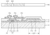
도 1을 참조하면, 본 실시예에 따른 평판 표시 장치는 기판(10) 위에 게이트 전극(21)과 동일층에 형성된 커패시터 제1 전극(31)을 포함하고, 투명 도전성 산화물로 구성된 반도체층(23)과 상기 반도체층(23)과 동일층에 동일 재료로 형성된 커패시터 제2 전극(33)을 포함한다. 또한, 커패시터 제1 전극(31)과 커패시터 제2 전극(33) 사이에 제1 절연막(12)이 구비되고, 커패시터 제2 전극(33) 상에 제2 절연막(14)이 구비된다. 그리고, 화소 전극(41)과 소스 전극(25a) 및 드레인 전극(25b) 사이에 상기 제1 절연막(12) 보다 유전율이 낮은 제3 절연막(16)이 구비된다.Referring to FIG. 1, the flat panel display according to the present embodiment includes a first electrode 31 formed on the same layer as a
도 2A 내지 2F는 도 1의 본 발명의 일 실시예에 따른 평판 표시 장치의 제조 방법을 개략적으로 도시한 단면도들이다.2A to 2F are cross-sectional views schematically illustrating a method of manufacturing a flat panel display device according to an embodiment of the present invention shown in FIG.
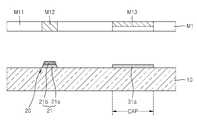
도 2A는 제1 포토 마스크(M1)을 이용한 제1 마스크 공정 후, 기판(10) 상에 형성된 게이트 전극(21) 및 커패시터 제1 전극(31)의 형상을 개략적으로 도시한 단면도이다.2A is a cross-sectional view schematically showing the shapes of the
제1 포토 마스크(M1)는 광투과부(M11), 광차단부(M12), 및 반투과부(M13)를 구비한 하프톤 마스크(half-tone mask)로 진행된다. 광차단부(M12)는 게이트 전극(21)의 패턴에 대응되도록 위치하고, 반투과부(M13)는 커패시터 제1 전극(31)의 패턴에 대응되도록 위치한다.The first photomask M1 proceeds to a half-tone mask having a light transmitting portion M11, a light blocking portion M12, and a transflective portion M13. The light shielding portion M12 is positioned to correspond to the pattern of the
기판(10)은 SiO2를 주성분으로 하는 투명 재질의 글라스재로 형성될 수 있다. 기판(10) 상에는 기판(10)의 평활성과 불순 원소의 침투를 차단하기 위하여 실리콘 옥사이드(Silicon oxide) 및/또는 실리콘 나이트라이드(Silicon nitride) 등을 포함하는 버퍼층(미도시)이 더 구비될 수 있다.The
게이트 전극(21)은 투명한 도전 재료로 형성된 제1 층(21a) 및 상기 제1 층(21a) 위에 위치하고 금속 재료로 형성된 제2 층(21b)으로 이루어진다.The
제1 층(21a)은 인듐틴옥사이드(indium tin oxide: ITO), 인듐징크옥사이드(indium zink oxide: IZO), 징크옥사이드(zink oxide: ZnO), 인듐옥사이드(indium oxide: In2O3), 인듐갈륨옥사이드(indium galium oxide: IGO), 및 알루미늄징크옥사이드(aluminium zink oxide: AZO) 가운데 선택된 적어도 하나 이상의 투명한 도전 재료를 포함할 수 있다.The
제2 층(21b)은 Ag, Mg, Al, Pt, Pd, Au, Ni, Nd, Ir, Cr, Li, Ca, Mo, Ti, W, MoW, 및 Al/Cu 가운데 선택된 하나 이상의 금속 재료를 포함할 수 있다.The
상기 도면에는 상세히 도시되지 않았지만, 상기 제1 층(21a)의 재료가 되는 투명한 도전층(미도시) 및 제2 층(21b)의 재료가 되는 금속층(미도시)을 기판(10) 위에 차례로 증착하고, 상기 금속층(미도시) 위에 포토레지스터(미도시)를 도포한 후, 노광 장치로 제1 포토 마스크(M11)에 노광한다. 노광 후, 현상(developing), 식각(etching), 및 스트립핑(stripping) 또는 에싱(ashing) 등과 같은 일련의 공정을 거친다.A metal layer (not shown), which is a material of the
제1 포토 마스크(M11)의 광차단부(M12)는 게이트 전극(21)의 패턴에 대응되도록 위치하기 때문에, 게이트 전극(21)의 제1 층(21a) 및 제2 층(21b)은 제1 포토 마스크(M11)로 동시에 식각되므로 제1 층(21a)과 제2 층(21b)의 외측 식각면은 동일면 상에 형성된다.The
상기 게이트 전극(21)과 이격되고, 상기 게이트 전극(21)과 동일층인 기판(10) 위에 커패시터 제1 전극(31)이 형성된다.A capacitor first electrode 31 is formed on the
커패시터 제1 전극(31)은 상기 게이트 전극(21)의 제1 층(21a)과 동일 재료로 형성된다. 따라서, 커패시터 제1 전극(31)은 인듐틴옥사이드(indium tin oxide: ITO), 인듐징크옥사이드(indium zink oxide: IZO), 징크옥사이드(zink oxide: ZnO), 인듐옥사이드(indium oxide: In2O3), 인듐갈륨옥사이드(indium galium oxide: IGO), 및 알루미늄징크옥사이드(aluminium zink oxide: AZO) 가운데 선택된 적어도 하나 이상의 투명한 도전 재료를 포함할 수 있다.The capacitor first electrode 31 is formed of the same material as the
상기 도면에는 상세히 도시되지 않았지만, 커패시터 제1 전극(31)은 전술한 게이트 전극(21)의 제1 층(21a)의 재료가 되는 투명한 도전층(미도시) 및 게이트 전극(21)의 제2 층(21b)의 재료가 되는 금속층(미도시) 중, 반투과부(M13)를 포함한 제1 포토 마스크(M11)를 이용한 공정에 의해 제2 층(21b)의 재료가 되는 금속층(미도시)이 제거되고, 제1 층(21a)의 재료가 되는 투명 도전층(미도시)이 남아 패턴을 형성한 것이다.Although not shown in detail in the drawing, the capacitor first electrode 31 is formed of a transparent conductive layer (not shown) as a material of the
도 2B는 제2 포토 마스크(M2)을 이용한 제2 마스크 공정 후, 제1 절연막(12) 위에 형성된 박막 트랜지스터의 반도체층(23) 및 커패시터 제2 전극(33)의 형상을 개략적으로 도시한 단면도이다.2B is a sectional view schematically showing the shapes of the
제2 포토 마스크(M2)는 광투과부(M21)과, 반도체층(23) 및 커패시터 제2 전극(33)에 대응되는 광차단부(M22)를 구비한다. 따라서, 반도체층(23)과 커패시터 제2 전극(33)은 동일 마스크 공정에서 함께 형성된다.The second photomask M2 includes a light transmitting portion M21 and a light blocking portion M22 corresponding to the
제1 절연막(12)은 게이트 전극(21)과 반도체층(23) 사이에 배치되어 게이트 절연막으로 기능 한다. 또한, 제1 절연막(12)은 커패시터 제1 전극(31)과 커패시터 제2 전극(33) 사이에 배치되어 커패시터의 유전막으로 기능 한다.The first
제1 절연막(12)은 실리콘 옥사이드(Silicon oxide) 또는 실리콘 나이트라이드(Silicon nitride)와 같은 투명한 무기 절연막을 사용할 수 있다.As the first insulating
이와 같은 무기 절연막은 후술할 제3 절연막(16)보다 유전율이 높아 커패시터의 용량을 높일 수 있다.Such an inorganic insulating film has a higher dielectric constant than the third insulating
반도체층(23) 및 커패시터 제2 전극(33)은 투명 도전성 산화물로 이루어진다. 투명 도전성 산화물은 갈륨(Ga), 인(In), 아연(Zn) 및 주석(Sn) 군에서 선택된 하나 이상의 원소, 및 산소(O)를 포함할 수 있다. 예를 들어, 상기 투명 도전성 산화물은 인듐갈륨징크옥사이드(indium galium zink oxide: InGaZnO), 인듐갈륨하프늄옥사이드(indium galium hafnium oxide: InGaHfO), 인듐징크하프늄옥사이드(indium zink hafnium oxide: InZnHfO), 및 인듐갈륨틴옥사이드(indium galium tin oxide: InGaTO) 가운데서 적어도 하나를 포함할 수 있다.The
상기와 같이 커패시터 제1 전극(31) 및 커패시터 제2 전극(33)이 모두 광 투과율이 좋은 재료로 형성되기 때문에, 평판 표시 장치의 개구율 및 투과율을 향상시킬 수 있다.As described above, since the capacitor first electrode 31 and the capacitor
도 2C는 제3 포토 마스크(M3)을 이용한 제3 마스크 공정 후 제2 절연막(14)에 형성된 다수의 콘택홀(14a, 14b, 14c)의 형상을 개략적으로 도시한 단면도이다. FIG. 2C is a cross-sectional view schematically showing the shapes of the plurality of
제3 포토 마스크(M3)는 반도체층(23)의 양 측부 및 커패시터 제2 전극(33)의 일부에 대응되는 광투과부(M31)와, 광차단부(M32)를 구비한다.The third photomask M3 includes a light transmitting portion M31 corresponding to both sides of the
상기 도면에는 커패시터 제2 전극(33)의 일부(14c)를 노출시키는 콘택홀(14c)이, 커패시터 제1 전극(31) 및 커패시터 제2 전극(33)이 중첩 배치된 커패시터 영역(CAP)의 외측에 형성되어 있지만 이는 일 예시이며 본 발명은 이에 한정되지 않음은 물론이다. 예를 들어, 상기 콘택홀(14c)는 상기 도면에 도시된 것보다 커패시터 제1 전극(31)에 가까운 위치, 또는 커패시터 제1 전극(31) 및 커패시터 제2 전극(33)이 중첩 배치된 커패시터 영역(CAP)에 형성된 커패시터 제2 전극(33) 상에 형성될 수도 있다.In the figure, a
제2 절연막(14)은 게이트 전극(21)에 대응되는 위치의 반도체층(23)의 채널 영역 위에 배치되어 에치 스토퍼(etch stopper)로 기능 할 수 있다.The second insulating
이와 같은 제2 절연막(14)은 전술한 제1 절연막(12)과 같이 실리콘 옥사이드(Silicon oxide) 또는 실리콘 나이트라이드(Silicon nitride)와 같은 투명한 무기 절연막을 사용할 수 있다.The second insulating
도 2D는 제4 포토 마스크(M4)을 이용한 제4 마스크 공정 후 제2 절연막(14)위에 형성된 소스 전극(25a) 및 드레인 전극(25b)의 형상을 개략적으로 도시한 단면도이다.2D is a cross-sectional view schematically showing the shapes of the
제4 포토 마스크(M4)는 광투과부(M41)과, 소스 전극(25a) 및 드레인 전극(25b)에 대응되는 광차단부(M42)를 구비한다.The fourth photomask M4 includes a light transmitting portion M41 and a light blocking portion M42 corresponding to the
소스 전극(25a) 및 드레인 전극(25b) 중 하나는 전술한 커패시터 제2 전극(33)에 형성된 콘택홀(14c)에 연결된다.One of the
도 2E는 제5 포토 마스크(M5)을 이용한 제5 마스크 공정 후 제3 절연막(16)에 형성된 비어홀(16a)의 형상을 개략적으로 도시한 단면도이다.FIG. 2E is a cross-sectional view schematically showing the shape of the via
제5 포토 마스크(M5)는 커패시터 제2 전극(33)의 일부에 대응되는 광투과부(M51)와, 광차단부(M52)를 구비한다.The fifth photomask M5 includes a light transmitting portion M51 corresponding to a part of the capacitor
제3 절연막(16)은 전술한 제1 절연막(12)보다 유전율이 작은 절연 재료를 사용하는 것이 바람직하다. 또한, 제3 절연막(16)은 전술한 제1 절연막(12)보다 두께가 두껍게 형성되는 것이 바람직하다. 이와 같은 제3 절연막(16)으로는 통상적으로 유기 절연막을 사용할 수 있다.The third
소스 전극(25a) 및 드레인 전극(25b)에 데이터 전압을 인가하는 데이터 배선(미도시)은 마스크 공정을 줄이기 위하여 소스 전극(25a) 및 드레인 전극(25b)과 동일층에 배치된다. 이때, 인접하는 다른 화소들 사이에 배치된 데이터 배선(미도시)은 인접한 화소 전극(41) 사이에 기생 커패시터를 형성시키고, 이러한 기생 커패시터는 인접한 화소의 데이터 신호에 영향을 줄 수 있다. A data line (not shown) for applying a data voltage to the
이와 같은 영향을 줄이기 위하여 인접한 화소 사이에 블랙 매트릭스를 배치하여야 하는데, 본 실시예와 같이 소스 전극(25a) 및 드레인 전극(25b)과 동일층에 배치되는 데이터 배선(미도시)과, 화소 전극(41) 사이에 유전율이 낮은 제3 절연막(16)을 배치하여 커패시터 용량을 줄임으로써, 기생 커패시터에 의한 인접한 화소의 데이터 신호에 영향을 줄일 수 있다. 또한 유기막으로 형성된 제3 절연막(16)의 두께를 두껍게 형성하여 기생 커패시터의 용량을 줄일 수 있다. 따라서, 인접한 화소 사이에 블랙 매트릭스를 배치할 필요가 없으므로, 제조 공정 및 제조 비용을 줄일 수 있다.In order to reduce such an influence, a black matrix should be disposed between adjacent pixels. Data lines (not shown) arranged on the same layer as the
한편, 상기 도면에는 비어홀(16a)이 커패시터 제1 전극(31) 및 커패시터 제2 전극(33)이 모두 배치된 커패시터 영역(CAP) 상의 커패시터 제2 전극(33) 상부를 직접 개구시키는 것으로 도시되어 있으나 이는 일 예시 일뿐 본 발명은 이에 한정되지 않는다. 즉, 상기 비어홀(16a)은 전술한 소스 전극(25a) 및 드레인 전극(25b) 중 하나를 직접 개구 시킬 수 있음은 물론이다.The figure shows that the via
도 2F는 제6 포토 마스크(M6)을 이용한 제6 마스크 공정 후 제3 절연막(16) 위에 형성된 화소 전극(41)의 형상을 개략적으로 도시한 단면도이다.2F is a cross-sectional view schematically showing the shape of the
제6 포토 마스크(M6)는 광투과부(M51)와, 화소 전극(41)에 대응되는 광차단부(M52)를 구비한다.The sixth photomask M6 includes a light transmitting portion M51 and a light blocking portion M52 corresponding to the
화소 전극(41)은 전술한 바와 같이 투과형 또는 반투과형 액정 표시 장치나, 배면 발광형 또는 양면 발광형 유기 발광 표시 장치의 경우 투명 전극으로 구비될 수 있다.The
그리고 상기 도면에는 도시되지 않았으나, 상기 화소 전극(41) 상에 대향 전극(미도시)이 더 구비되고, 상기 화소 전극(41)과 대향 전극(미도시) 사이에 액정이 구비된 액정 표시 장치로 사용될 수 있다. 이 경우, 전술한 커패시터 제1 전극(31)에는 Vcom, Vgh, 또는 Vgl 등이 직접 인가될 수 있다.Although not shown in the drawing, a liquid crystal display device having a counter electrode (not shown) on the
상술한 본 발명의 제1 실시예에 따른 평판 표시 장치는, 커패시터 제1 전극(31) 및 커패시터 제2 전극(33)이 모두 광 투과율이 좋은 재료로 형성되기 때문에 개구율 및 투과율을 향상시킬 수 있다. 또한, 유전율이 큰 제1 절연막(12)을 커패시터의 유전막으로 사용함으로써 커패시터의 용량을 늘릴 수 있다. 또한 유전율이 작은 제3 절연막(16)을 데이터 배선(미도시)과 화소 전극(41) 사이에 배치함으로써 인접한 화소에 미치는 영향을 줄일 수 있다.In the flat panel display device according to the first embodiment of the present invention, both the capacitor first electrode 31 and the capacitor
도 3은 본 발명의 다른 실시예에 따른 평판 표시 장치를 개략적으로 도시한 단면도이다. 동일한 참조부호는 전술한 실시예에 따른 평판 표시 장치와 동일한 구성을 나타낸다.3 is a cross-sectional view schematically showing a flat panel display according to another embodiment of the present invention. The same reference numerals denote the same components as those of the flat panel display device according to the embodiment described above.
도 3을 참조하면, 본 실시예에 따른 평판 표시 장치는 전술한 실시예와 마찬가지로 기판(10) 위에 게이트 전극(21)과 동일층에 형성된 커패시터 제1 전극(31)을 포함하고, 투명 도전성 산화물로 구성된 반도체층(23)과 상기 반도체층(23)과 동일층에 동일 재료로 형성된 커패시터 제2 전극(33)을 포함한다. 또한, 커패시터 제1 전극(31)과 커패시터 제2 전극(33) 사이에 제1 절연막(12)이 구비되고, 화소 전극(41)과 소스 전극(25a) 및 드레인 전극(25b) 사이에 상기 제1 절연막(12) 보다 유전율이 낮은 제3 절연막(16)이 구비된다.3, the flat panel display device according to the present embodiment includes a capacitor first electrode 31 formed on the same layer as the
그러나, 본 실시예에서 커패시터 제2 전극(33) 상의 제2 절연막(14)은 제거된다. 제2 절연막(14)의 제거는 전술한 실시예의 콘택홀(14a, 14b, 14c)을 형성하는 제3 마스크 공정에서, 상기 콘택홀(14a, 14b, 14c)의 형성과 동시에 수행할 수 있다.However, in this embodiment, the second insulating
상기와 같이 커패시터 제2 전극(33) 상의 제2 절연막(14)을 제거함으로써, 투과형 또는 반투과형 액정 표시 장치나, 배면 발광형 또는 양면 발광형 유기 발광 표시 장치의 경우, 투과율을 더욱 향상시킬 수 있다.By removing the second insulating
한편, 상기 도면은 커패시터 제2 전극(33)에 대응되는 영역의 제2 절연막(14)만 제거된 형상을 도시하고 있지만, 본 발명은 이에 한정되지 않는다. 예를 들어, 반도체층(23)의 채널 영역 상부에만 에치 스토퍼로 기능하는 제2 절연막(14)을 남기고 나머지 제2 절연막(14)의 전체를 제거할 수도 있다.In the meantime, the figure shows a shape in which only the second insulating
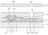
도 4는 본 발명의 또 다른 실시예에 따른 평판 표시 장치를 개략적으로 도시한 단면도이다. 동일한 참조부호는 전술한 실시예에 따른 평판 표시 장치와 동일한 구성을 나타낸다.4 is a cross-sectional view schematically illustrating a flat panel display according to another embodiment of the present invention. The same reference numerals denote the same components as those of the flat panel display device according to the embodiment described above.
도 4를 참조하면, 본 실시예에 따른 평판 표시 장치는 전술한 실시예와 마찬가지로 기판(10) 위에 게이트 전극(21)과 동일층에 형성된 커패시터 제1 전극(31)을 포함하고, 투명 도전성 산화물로 구성된 반도체층(23)과 상기 반도체층(23)과 동일층에 동일 재료로 형성된 커패시터 제2 전극(33)을 포함한다. 또한, 커패시터 제1 전극(31)과 커패시터 제2 전극(33) 사이에 제1 절연막(12)이 구비되고, 화소 전극(41)과 소스 전극(25a) 및 드레인 전극(25b) 사이에 상기 제1 절연막(12) 보다 유전율이 낮은 제3 절연막(16)이 구비된다.Referring to FIG. 4, the flat panel display according to the present embodiment includes a capacitor first electrode 31 formed on the same layer as the
그러나, 본 실시예에서 커패시터 제2 전극(33) 상의 제2 절연막(14)은 제거되고, 제2 절연막(14)이 제거된 커패시터 제2 전극(33) 상에 커패시터 제3 전극(35)이 더 구비된다. 이때, 제1 절연막(14)과 제2 절연막(14)은 동일 재료로 형성되며 바람직하게는 실리콘 옥사이드로 형성된다.In this embodiment, however, the second insulating
커패시터 제3 전극(35)은 전술한 제4 마스크 공정에서 소스 전극(25a) 및 드레인 전극(25b)과 동시에 형성되고, 소스 전극(25a) 및 드레인 전극(25b)과 동일 재료로 형성된다.The capacitor
만약 게이트 전극(21)과 동일층에 형성된 커패시터 제1 전극(31)과, 소스 및 드레인 전극(25a, 25b)과 동일층에 형성된 커패시터 제3 전극(35)으로 커패시터를 형성할 경우, 제1 전극(31)과 제3 전극(35) 사이에는 제1 절연막(12)과 제2 절연막(14)이 유전막으로 기능 하게 된다. 즉, 커패시터의 두 전극 사이에 두개 층의 유전막이 개재되기 때문에 한 층의 유전막이 개재되는 것에 비하여 커패시터 용량이 줄어든다. 따라서 줄어든 용량을 보상하기 위하여 커패시터 면적을 늘려야 하고, 커패시터 면적을 늘릴수록 개구율 및 투과율이 감소하게 된다. 그러나 본 실시예에서는 한 층의 유전막만이 개재됨으로써 커패시터의 용량 감소를 방지할 수 있다.If a capacitor is formed of the capacitor first electrode 31 formed on the same layer as the
한편, 반도체층(23)과 직접 접촉하는 게이트 절연막으로 기능하는 제1 절연막(12)과 에치 스토퍼로 기능하는 제2 절연막(14)은, 반도체 소자 특성을 향상시키기 위해서 수소 함유량이 작은 실리콘 옥사이드를 사용하는 것이 바람직하다. 그러나 제1 절연막(12)과 제2 절연막(14)을 모두 동일 재료인 실리콘 옥사이드로 형성할 경우, 제2 절연막(14) 에칭시 제1 절연막(12)도 손상을 받게 된다. 그러나 본 실시예에서는 제2 절연막(14)과 제1 절연막(12) 사이에 투명 도전성 산화물 반도체를 포함하는 커패시터 제2 전극(33)이 개재되어 제1 절연막(12)의 식각을 저지한다. 따라서, 제1 절연막(12)의 손상 없이 제2 절연막(14)을 식각하여 커패시터의 용량을 증가시키고 반도체 소자의 특성을 향상시킬 수 있다.On the other hand, the first insulating
한편, 상기 도면은 커패시터 제1 전극(31)에 대응되는 영역의 제2 절연막(14)만 제거된 형상을 도시하고 있지만, 본 발명은 이에 한정되지 않는다. 예를 들어, 반도체층(23)의 채널 영역 상부에만 에치 스토퍼로 기능하는 제2 절연막(14)을 남기고 제2 절연막(14)의 전체를 제거할 수도 있다.In the meantime, the figure shows the shape in which only the second insulating
상기 도면들에 도시된 구성요소들은 설명의 편의상 확대 또는 축소되어 표시될 수 있으므로, 도면에 도시된 구성요소들의 크기나 형상에 본 발명이 구속되는 것은 아니며, 본 기술 분야의 통상의 지식을 가진 자라면 이로부터 다양한 변형 및 균등한 다른 실시예가 가능하다는 점을 이해할 것이다. 따라서 본 발명의 진정한 기술적 보호범위는 첨부된 특허청구범위의 기술적 사상에 의하여 정해져야 할 것이다.It is to be understood that both the foregoing general description and the following detailed description are exemplary and explanatory and are not restrictive of the invention, It will be understood that various modifications and equivalent embodiments may be possible. Accordingly, the true scope of the present invention should be determined by the technical idea of the appended claims.
10: 기판12: 제1 절연막
14: 제2 절연막16: 제3 절연막
20: 박막 트랜지스터21: 게이트 전극
23: 반도체층25a, 25b: 소스 전극, 드레인 전극
31: 커패시터 제1 전극33: 커패시터 제2 전극
35: 커패시터 제3 전극41: 화소 전극10: substrate 12: first insulating film
14: second insulating film 16: third insulating film
20: Thin film transistor 21: Gate electrode
23:
31: Capacitor first electrode 33: Capacitor second electrode
35: capacitor third electrode 41: pixel electrode
Claims (25)
Translated fromKorean제1 절연막을 사이에 두고 상기 게이트 전극 위에 배치되고, 투명 도전성 산화물을 포함하는 반도체층;
상기 게이트 전극과 동일층에 배치되고 투명 도전층으로 형성된 커패시터 제1 전극, 및 상기 제1 절연막을 사이에 두고 상기 반도체층과 동일 재료로 형성되며, 상기 반도체층과 동일층에 배치된 커패시터 제2전극;
제2 절연막을 사이에 두고 서로 이격되어 배치되고, 상기 반도체층 및 상기 커패시터 제2 전극과 연결된 소스 전극과 드레인 전극;
상기 소스 전극 및 드레인 전극을 덮는 제3 절연막; 및
상기 제3 절연막 위에 배치되고, 상기 기판에 수직인 방향으로 상기 커패시터의 제1 전극 및 상기 커패시터의 제2 전극과 오버랩되어 배치되고, 상기 제3 절연막에 형성된 비아홀을 통하여 상기 커패시터의 제2 전극의 상면에 직접 접촉하고, 상기 소스 전극 및 드레인 전극 중 하나와 연결된 화소 전극;을 포함하는 평판 표시 장치.A gate electrode disposed on the substrate;
A semiconductor layer disposed on the gate electrode with a first insulating film therebetween, the semiconductor layer including a transparent conductive oxide;
A capacitor first electrode formed on the same layer as the gate electrode and formed of a transparent conductive layer, and a capacitor second electrode formed on the same layer as the semiconductor layer with the first insulating film interposed therebetween, electrode;
A source electrode and a drain electrode which are disposed apart from each other with a second insulating film therebetween and are connected to the semiconductor layer and the capacitor second electrode;
A third insulating layer covering the source electrode and the drain electrode; And
A first electrode of the capacitor and a second electrode of the capacitor are arranged in the direction perpendicular to the substrate, the first electrode of the capacitor and the second electrode of the capacitor are arranged to overlap with each other, And a pixel electrode that is in direct contact with the upper surface and is connected to one of the source electrode and the drain electrode.
상기 게이트 전극은 투명 도전층, 및 상기 투명 도전층 위에 배치된 금속층을 포함하고, 상기 게이트 전극의 투명 도전층은 상기 커패시터의 제1 전극과 동일한 재료를 포함하는 평판 표시 장치.The method according to claim 1,
Wherein the gate electrode includes a transparent conductive layer and a metal layer disposed on the transparent conductive layer, and the transparent conductive layer of the gate electrode includes the same material as the first electrode of the capacitor.
상기 투명 도전층 및 상기 금속층은 외측 식각면은 동일면 상에 위치하는 평판 표시 장치.3. The method of claim 2,
Wherein the transparent conductive layer and the metal layer are located on the same plane.
상기 커패시터 제1 전극은 인듐틴옥사이드(indium tin oxide: ITO), 인듐징크옥사이드(indium zink oxide: IZO), 징크옥사이드(zink oxide: ZnO), 인듐옥사이드(indium oxide: In2O3), 인듐갈륨옥사이드(indium galium oxide: IGO), 및 알루미늄징크옥사이드(aluminium zink oxide: AZO)을 포함하는 그룹에서 선택된 적어도 하나를 포함하는 평판 표시 장치.The method according to claim 1,
The first electrode of the capacitor may be formed of indium tin oxide (ITO), indium zinc oxide (IZO), zinc oxide (ZnO), indium oxide (In2O3), indium gallium oxide indium gallium oxide (IGO), and aluminum zinc oxide (AZO).
상기 투명 도전성 산화물은 갈륨(Ga), 인(In), 아연(Zn) 및 주석(Sn) 군에서 선택된 하나 이상의 원소, 및 산소(O)를 포함하는 평판 표시 장치.The method according to claim 1,
Wherein the transparent conductive oxide includes at least one element selected from the group consisting of gallium (Ga), indium (In), zinc (Zn) and tin (Sn), and oxygen (O).
상기 제1 절연막은 상기 제3 절연막보다 큰 유전율을 갖는 평판 표시 장치.The method according to claim 1,
Wherein the first insulating film has a larger dielectric constant than the third insulating film.
상기 제1 절연막은 무기 절연물을 포함하고, 상기 제3 절연막은 유기 절연물을 포함하는 평판 표시 장치.The method according to claim 1,
Wherein the first insulating film includes an inorganic insulating material, and the third insulating film includes an organic insulating material.
상기 소스 전극 및 드레인 전극과 동일층에 상기 소스 전극 및 드레인 전극에 데이터 전압을 인가하는 데이터 배선이 구비된 평판 표시 장치.The method according to claim 1,
And a data line for applying a data voltage to the source electrode and the drain electrode in the same layer as the source electrode and the drain electrode.
상기 제3 절연막은 상기 제1 절연막보다 두꺼운 평판 표시 장치.The method according to claim 1,
Wherein the third insulating film is thicker than the first insulating film.
상기 커패시터 제2 전극 위의 상기 제2 절연막은 제거되고, 상기 커패시터 제2 전극은 상기 제3 절연막과 직접 접촉하는 평판 표시 장치.The method according to claim 1,
Wherein the second insulating film on the capacitor second electrode is removed, and the capacitor second electrode is in direct contact with the third insulating film.
상기 커패시터 제2 전극과 상기 제3 절연막 사이에 배치되고, 상기 소스 전극 및 드레인 전극과 동일 재료로 형성된 커패시터 제3 전극을 더 구비한 평판 표시 장치.12. The method of claim 11,
And a capacitor third electrode disposed between the capacitor second electrode and the third insulating film and formed of the same material as the source electrode and the drain electrode.
상기 제1 절연막 및 상기 제2 절연막은 동일한 절연물을 포함하는 평판 표시 장치.13. The method of claim 12,
Wherein the first insulating film and the second insulating film include the same insulating material.
상기 제1 절연막 및 상기 제2 절연막은 실리콘 옥사이드(silicon oxide:SiOx)를 포함하는 평판 표시 장치.14. The method of claim 13,
Wherein the first insulating film and the second insulating film comprise silicon oxide (SiOx).
상기 화소 전극은 투명 전극인 평판 표시 장치.The method according to claim 1,
Wherein the pixel electrode is a transparent electrode.
상기 화소 전극에 대향하는 대향 전극을 더 포함하고, 상기 화소 전극과 상기 대향 전극 사이에 액정이 포함된 평판 표시 장치.The method according to claim 1,
Further comprising a counter electrode facing the pixel electrode, wherein liquid crystal is contained between the pixel electrode and the counter electrode.
상기 커패시터 제1 전극에 Vcom, Vgh, 또는 Vgl이 인가되는 평판 표시 장치.18. The method of claim 17,
And Vcom, Vgh, or Vgl is applied to the first electrode of the capacitor.
상기 화소 전극에 대향하는 대향 전극을 더 포함하고, 상기 화소 전극과 상기 대향 전극 사이에 유기 발광층이 포함된 평판 표시 장치.The method according to claim 1,
And a counter electrode facing the pixel electrode, wherein the organic light emitting layer is disposed between the pixel electrode and the counter electrode.
제1 절연막을 사이에 두고, 투명 도전물질을 포함하고, 상기 박막 트랜지스터의 반도체층 및 커패시터 제2 전극을 형성하는 제2 마스크 공정;
제2 절연막을 형성하고, 상기 제2 절연막을 관통하여 상기 반도체층의 일부 및 커패시터 제2 전극의 일부를 노출시키는 콘택홀을 형성하는 제3 마스크 공정;
상기 콘택홀을 통해 상기 반도체층 및 커패시터 제2 전극과 연결된 소스 전극 및 드레인 전극을 형성하는 제4 마스크 공정;
상기 소스 전극 및 드레인 전극을 덮는 제3 절연막을 형성하고, 상기 제3 절연막에 비아홀을 형성하는 제5 마스크 공정; 및
상기 기판에 수직인 방향으로 상기 커패시터의 제1 전극 및 상기 커패시터의 제2 전극과 오버랩 되도록 상기 비아홀을 통하여 상기 커패시터의 제2 전극의 상면에 직접 접촉하도록 형성하고, 상기 소스 전극 및 드레인 전극 중 하나에 연결되는 화소 전극을 형성하는 제6 마스크 공정;을 포함하는 평판 표시 장치의 제조 방법.A first mask process for forming a gate electrode and a capacitor first electrode of a thin film transistor including a transparent conductive material on a substrate;
A second masking step of forming a semiconductor layer and a capacitor second electrode of the thin film transistor including a transparent conductive material with a first insulating film interposed therebetween;
Forming a second insulating film, forming a contact hole through the second insulating film to expose a part of the semiconductor layer and a part of the capacitor second electrode;
A fourth mask process for forming a source electrode and a drain electrode connected to the semiconductor layer and the capacitor second electrode through the contact hole;
A fifth masking step of forming a third insulating film covering the source electrode and the drain electrode, and forming a via hole in the third insulating film; And
Wherein the first electrode of the capacitor and the second electrode of the capacitor are formed to be in direct contact with the upper surface of the second electrode of the capacitor through the via hole so as to overlap the first electrode of the capacitor and the second electrode of the capacitor in a direction perpendicular to the substrate, And a sixth masking step of forming a pixel electrode connected to the pixel electrode.
상기 제1 마스크 공정에서, 상기 게이트 전극은 투명 도전층 및 상기 투명 도전층 위에 배치된 금속층을 포함하고, 상기 커패시터 제1전극은 상기 투명 도전층과 동일층에 동일 재료로 형성되는 평판 표시 장치의 제조 방법.21. The method of claim 20,
In the first mask process, the gate electrode includes a transparent conductive layer and a metal layer disposed on the transparent conductive layer, and the capacitor first electrode is formed of the same material as the transparent conductive layer, Gt;
상기 제1 마스크 공정에서, 광투과부, 상기 커패시터 제1전극에 대응되는 반투과부, 및 상기 게이트 전극에 대응되는 광차단부를 구비한 하프톤 마스크를 사용하는 평판 표시 장치의 제조 방법.22. The method of claim 21,
Wherein in the first masking step, a halftone mask having a light transmitting portion, a transflecting portion corresponding to the first electrode of the capacitor, and a light shielding portion corresponding to the gate electrode is used.
상기 제2 마스크 공정에서, 상기 반도체층 및 커패시터 제2 전극은 투명 도전성 산화물로 형성하는 평판 표시 장치의 제조 방법.21. The method of claim 20,
In the second mask process, the semiconductor layer and the capacitor second electrode are formed of a transparent conductive oxide.
상기 제3 마스크 공정에서, 상기 커패시터 제2 전극 위의 상기 제2 절연막을 제거하는 평판 표시 장치의 제조 방법.21. The method of claim 20,
And removing the second insulating film on the capacitor second electrode in the third masking step.
상기 제4 마스크 공정에서, 상기 제2 절연막이 제거된 상기 커패시터 제2 전극 위에 상기 소스 및 드레인 전극과 동일 재료로 커패시터 제3 전극을 형성하는 평판 표시 장치의 제조 방법.25. The method of claim 24,
Wherein the capacitor third electrode is formed of the same material as the source and drain electrodes on the second electrode of the capacitor from which the second insulating film is removed in the fourth mask process.
Priority Applications (4)
| Application Number | Priority Date | Filing Date | Title |
|---|---|---|---|
| KR1020100057567AKR101783352B1 (en) | 2010-06-17 | 2010-06-17 | Flat panel display apparatus and manufacturing method of the same |
| US13/064,651US8749725B2 (en) | 2010-06-17 | 2011-04-06 | Flat panel display apparatus and method of manufacturing the same |
| CN201110122768.2ACN102290421B (en) | 2010-06-17 | 2011-05-05 | The method of panel display apparatus and this panel display apparatus of manufacture |
| TW100116556ATWI567800B (en) | 2010-06-17 | 2011-05-11 | Flat display device and method of manufacturing same |
Applications Claiming Priority (1)
| Application Number | Priority Date | Filing Date | Title |
|---|---|---|---|
| KR1020100057567AKR101783352B1 (en) | 2010-06-17 | 2010-06-17 | Flat panel display apparatus and manufacturing method of the same |
Publications (2)
| Publication Number | Publication Date |
|---|---|
| KR20110137562A KR20110137562A (en) | 2011-12-23 |
| KR101783352B1true KR101783352B1 (en) | 2017-10-10 |
Family
ID=45327863
Family Applications (1)
| Application Number | Title | Priority Date | Filing Date |
|---|---|---|---|
| KR1020100057567AActiveKR101783352B1 (en) | 2010-06-17 | 2010-06-17 | Flat panel display apparatus and manufacturing method of the same |
Country Status (4)
| Country | Link |
|---|---|
| US (1) | US8749725B2 (en) |
| KR (1) | KR101783352B1 (en) |
| CN (1) | CN102290421B (en) |
| TW (1) | TWI567800B (en) |
Families Citing this family (40)
| Publication number | Priority date | Publication date | Assignee | Title |
|---|---|---|---|---|
| TWI743509B (en)* | 2011-05-05 | 2021-10-21 | 日商半導體能源研究所股份有限公司 | Semiconductor device and method for manufacturing the same |
| CN103186002A (en)* | 2011-12-27 | 2013-07-03 | 群康科技(深圳)有限公司 | Display device and image display system comprising same |
| TW201327833A (en)* | 2011-12-27 | 2013-07-01 | Chimei Innolux Corp | Display device and image display system including the same |
| CN104081879B (en)* | 2012-01-18 | 2017-03-01 | 株式会社日本有机雷特显示器 | Electronic installation and its manufacture method |
| KR20130089044A (en)* | 2012-02-01 | 2013-08-09 | 삼성디스플레이 주식회사 | Semiconductor device and flat panel display device having the same |
| CN102646684B (en)* | 2012-02-17 | 2015-03-11 | 京东方科技集团股份有限公司 | Array substrate, manufacturing method thereof and display device |
| KR101899878B1 (en)* | 2012-03-30 | 2018-09-18 | 엘지디스플레이 주식회사 | Organic light emitting diode display device and fabricating method of the same |
| KR101998124B1 (en)* | 2012-07-24 | 2019-07-09 | 엘지디스플레이 주식회사 | Array substrate and method of fabricating the same |
| US9625764B2 (en)* | 2012-08-28 | 2017-04-18 | Semiconductor Energy Laboratory Co., Ltd. | Display device and electronic device |
| CN104620390A (en)* | 2012-09-13 | 2015-05-13 | 株式会社半导体能源研究所 | Semiconductor device |
| TWI611566B (en)* | 2013-02-25 | 2018-01-11 | 半導體能源研究所股份有限公司 | Display device and electronic device |
| JP6083089B2 (en)* | 2013-03-27 | 2017-02-22 | 株式会社Joled | Semiconductor device, display device and electronic apparatus |
| US9915848B2 (en)* | 2013-04-19 | 2018-03-13 | Semiconductor Energy Laboratory Co., Ltd. | Display device and electronic device |
| TWI687748B (en)* | 2013-06-05 | 2020-03-11 | 日商半導體能源研究所股份有限公司 | Display device and electronic device |
| JP6201465B2 (en)* | 2013-07-08 | 2017-09-27 | ソニー株式会社 | Display device, driving method of display device, and electronic apparatus |
| JP2015015440A (en)* | 2013-07-08 | 2015-01-22 | ソニー株式会社 | SEMICONDUCTOR DEVICE, ITS MANUFACTURING METHOD, DISPLAY DEVICE, AND ELECTRONIC DEVICE |
| KR102130139B1 (en)* | 2013-07-30 | 2020-07-03 | 엘지디스플레이 주식회사 | Organic Light Emitting Diode Display Having Thin Film Transistor Substrate Using Oxide Semiconductor And Method For Manufacturing The Same |
| CN103456687B (en)* | 2013-09-02 | 2015-12-09 | 合肥京东方光电科技有限公司 | A kind of array base palte and preparation method thereof |
| KR102049793B1 (en) | 2013-11-15 | 2020-01-08 | 엘지디스플레이 주식회사 | Organic light emitting display device |
| JP2015108731A (en)* | 2013-12-05 | 2015-06-11 | ソニー株式会社 | SEMICONDUCTOR DEVICE, ITS MANUFACTURING METHOD, DISPLAY DEVICE, AND ELECTRONIC DEVICE |
| JP2015122417A (en)* | 2013-12-24 | 2015-07-02 | ソニー株式会社 | Semiconductor device and method of manufacturing the same, display device, and electronic apparatus |
| CN104617038A (en)* | 2015-01-13 | 2015-05-13 | 深圳市华星光电技术有限公司 | Manufacturing method of array substrate, array substrate and a display panel |
| KR102369300B1 (en)* | 2015-02-24 | 2022-03-03 | 삼성디스플레이 주식회사 | Organic light emitting display device and manufacturing method of the same |
| CN105489502B (en)* | 2016-01-19 | 2018-04-20 | 深圳市华星光电技术有限公司 | The manufacture method of thin-film transistor structure |
| JP6970511B2 (en)* | 2016-02-12 | 2021-11-24 | 株式会社半導体エネルギー研究所 | Transistor |
| CN105655408A (en)* | 2016-03-14 | 2016-06-08 | 京东方科技集团股份有限公司 | Thin film transistor, array substrate and manufacture and driving method of array substrate and display device |
| KR101859484B1 (en)* | 2016-05-30 | 2018-05-21 | 엘지디스플레이 주식회사 | Display device and method of manufacturing the same |
| KR102568924B1 (en) | 2016-06-14 | 2023-08-22 | 삼성디스플레이 주식회사 | Display device and rear-view mirror module including the same |
| CN106098706B (en)* | 2016-07-22 | 2019-02-22 | 京东方科技集团股份有限公司 | Array substrate, method for making the same, and display device |
| US10249695B2 (en)* | 2017-03-24 | 2019-04-02 | Apple Inc. | Displays with silicon and semiconducting-oxide top-gate thin-film transistors |
| JP2019117342A (en)* | 2017-12-27 | 2019-07-18 | シャープ株式会社 | Active matrix substrate, manufacturing method therefor, and liquid crystal display device |
| KR102469793B1 (en)* | 2017-12-29 | 2022-11-22 | 삼성디스플레이 주식회사 | Display device |
| KR102538000B1 (en)* | 2018-03-29 | 2023-05-31 | 삼성디스플레이 주식회사 | Display apparatus |
| CN110071069B (en)* | 2019-04-19 | 2021-11-23 | 深圳市华星光电半导体显示技术有限公司 | Display back plate and manufacturing method thereof |
| KR102694186B1 (en)* | 2019-06-21 | 2024-08-12 | 삼성디스플레이 주식회사 | Display device and method of manufacturing the same |
| CN110707101A (en)* | 2019-10-16 | 2020-01-17 | 深圳市华星光电半导体显示技术有限公司 | Array substrate and manufacturing method thereof, and display panel |
| CN110783490A (en)* | 2019-11-13 | 2020-02-11 | 合肥京东方卓印科技有限公司 | Display panel and preparation method thereof |
| CN111029344A (en)* | 2019-11-19 | 2020-04-17 | 深圳市华星光电半导体显示技术有限公司 | Array substrate and preparation method thereof |
| CN111668242A (en)* | 2020-07-02 | 2020-09-15 | 深圳市华星光电半导体显示技术有限公司 | OLED display panel and preparation method thereof |
| CN115312546A (en)* | 2022-10-10 | 2022-11-08 | 广州华星光电半导体显示技术有限公司 | Array substrate, preparation method thereof and display panel |
Family Cites Families (16)
| Publication number | Priority date | Publication date | Assignee | Title |
|---|---|---|---|---|
| US6346730B1 (en)* | 1999-04-06 | 2002-02-12 | Semiconductor Energy Laboratory Co., Ltd. | Liquid crystal display device having a pixel TFT formed in a display region and a drive circuit formed in the periphery of the display region on the same substrate |
| KR101002492B1 (en) | 2002-08-02 | 2010-12-17 | 이데미쓰 고산 가부시키가이샤 | Sputtering target, sintered compact, conductive film manufactured using these, organic EL element, and board | substrate used for this |
| US20050017244A1 (en) | 2003-07-25 | 2005-01-27 | Randy Hoffman | Semiconductor device |
| CN1998087B (en) | 2004-03-12 | 2014-12-31 | 独立行政法人科学技术振兴机构 | Amorphous oxide and thin film transistor |
| US7297977B2 (en) | 2004-03-12 | 2007-11-20 | Hewlett-Packard Development Company, L.P. | Semiconductor device |
| AU2005302964B2 (en) | 2004-11-10 | 2010-11-04 | Canon Kabushiki Kaisha | Field effect transistor employing an amorphous oxide |
| EP2453481B1 (en) | 2004-11-10 | 2017-01-11 | Canon Kabushiki Kaisha | Field effect transistor with amorphous oxide |
| KR101240652B1 (en)* | 2006-04-24 | 2013-03-08 | 삼성디스플레이 주식회사 | Thin film transistor array panel for display and manufacturing method of the same |
| KR20080008618A (en) | 2006-07-20 | 2008-01-24 | 삼성전자주식회사 | LCD Display |
| US7772021B2 (en)* | 2006-11-29 | 2010-08-10 | Samsung Electronics Co., Ltd. | Flat panel displays comprising a thin-film transistor having a semiconductive oxide in its channel and methods of fabricating the same for use in flat panel displays |
| KR101346861B1 (en) | 2006-11-30 | 2014-01-02 | 엘지디스플레이 주식회사 | Liquid crystal display device and method of fabricating the same |
| CN100550396C (en)* | 2007-04-26 | 2009-10-14 | 友达光电股份有限公司 | Pixel and forming method thereof, storage capacitor, display panel and photoelectric device |
| KR101484297B1 (en)* | 2007-08-31 | 2015-01-19 | 가부시키가이샤 한도오따이 에네루기 켄큐쇼 | Display device and method of manufacturing display device |
| TWI360885B (en)* | 2007-10-26 | 2012-03-21 | Au Optronics Corp | Pixel structure and fabrication method thereof |
| CN100550325C (en)* | 2007-11-07 | 2009-10-14 | 友达光电股份有限公司 | A kind of thin film transistor and its manufacturing method |
| KR101375831B1 (en) | 2007-12-03 | 2014-04-02 | 삼성전자주식회사 | Display device using oxide semiconductor thin film transistor |
- 2010
- 2010-06-17KRKR1020100057567Apatent/KR101783352B1/enactiveActive
- 2011
- 2011-04-06USUS13/064,651patent/US8749725B2/enactiveActive
- 2011-05-05CNCN201110122768.2Apatent/CN102290421B/enactiveActive
- 2011-05-11TWTW100116556Apatent/TWI567800B/enactive
Also Published As
| Publication number | Publication date |
|---|---|
| US20110309362A1 (en) | 2011-12-22 |
| TW201232629A (en) | 2012-08-01 |
| TWI567800B (en) | 2017-01-21 |
| CN102290421A (en) | 2011-12-21 |
| KR20110137562A (en) | 2011-12-23 |
| CN102290421B (en) | 2016-01-20 |
| US8749725B2 (en) | 2014-06-10 |
Similar Documents
| Publication | Publication Date | Title |
|---|---|---|
| KR101783352B1 (en) | Flat panel display apparatus and manufacturing method of the same | |
| US8598589B2 (en) | Array substrate, method of manufacturing the array substrate, and display apparatus including the array substrate | |
| KR101710179B1 (en) | Flat panel display apparatus and manufacturing method of the same | |
| US9711542B2 (en) | Method for fabricating display panel | |
| US20170090229A1 (en) | Semiconductor device, display device and method for manufacturing semiconductor device | |
| JP4406415B2 (en) | Array substrate for liquid crystal display device and manufacturing method thereof | |
| US8045077B2 (en) | Liquid crystal display device and fabrication method thereof | |
| US8193534B2 (en) | Array substrate of thin film transistor liquid crystal display and method of manufacturing the same | |
| KR101900170B1 (en) | Method for manufacturing array substrate, array substrate and display device | |
| WO2015081652A1 (en) | Array substrate and manufacturing method thereof and display device | |
| US20190043898A1 (en) | Array substrate motherboard, method for manufacturing the same, and display device | |
| US8357937B2 (en) | Thin film transistor liquid crystal display device | |
| KR20110056962A (en) | Method of manufacturing thin film transistor substrate | |
| US20090085032A1 (en) | Pixel structure and fabricating method thereof | |
| US20120241746A1 (en) | Electrophoresis display and manufacturing method | |
| WO2011161875A1 (en) | Substrate for display device and process for production thereof, and display device | |
| KR101626362B1 (en) | Method of fabricating substrate for thin film transistor | |
| US9035364B2 (en) | Active device and fabricating method thereof | |
| KR102090600B1 (en) | TFT array substrate and manufacturing methods therefor | |
| CN102830531B (en) | TFT (Thin Film Transistor) array substrate, manufacturing method and liquid crystal display device | |
| CN101207092B (en) | Liquid crystal display device and manufacturing method thereof | |
| CN105304639A (en) | Manufacturing method of thin-film transistor array substrate | |
| CN202693953U (en) | TFT (Thin Film Transistor) array substrate and liquid crystal display device | |
| US20050196911A1 (en) | Method for fabricating active-matrix display device | |
| KR101471149B1 (en) | Thin film transistor substrate and method of manufacturing the same |
Legal Events
| Date | Code | Title | Description |
|---|---|---|---|
| PA0109 | Patent application | Patent event code:PA01091R01D Comment text:Patent Application Patent event date:20100617 | |
| PG1501 | Laying open of application | ||
| N231 | Notification of change of applicant | ||
| PN2301 | Change of applicant | Patent event date:20120725 Comment text:Notification of Change of Applicant Patent event code:PN23011R01D | |
| A201 | Request for examination | ||
| PA0201 | Request for examination | Patent event code:PA02012R01D Patent event date:20150617 Comment text:Request for Examination of Application Patent event code:PA02011R01I Patent event date:20100617 Comment text:Patent Application | |
| E902 | Notification of reason for refusal | ||
| PE0902 | Notice of grounds for rejection | Comment text:Notification of reason for refusal Patent event date:20161107 Patent event code:PE09021S01D | |
| AMND | Amendment | ||
| E601 | Decision to refuse application | ||
| PE0601 | Decision on rejection of patent | Patent event date:20170524 Comment text:Decision to Refuse Application Patent event code:PE06012S01D Patent event date:20161107 Comment text:Notification of reason for refusal Patent event code:PE06011S01I | |
| AMND | Amendment | ||
| PX0901 | Re-examination | Patent event code:PX09011S01I Patent event date:20170524 Comment text:Decision to Refuse Application Patent event code:PX09012R01I Patent event date:20170207 Comment text:Amendment to Specification, etc. | |
| PX0701 | Decision of registration after re-examination | Patent event date:20170710 Comment text:Decision to Grant Registration Patent event code:PX07013S01D Patent event date:20170623 Comment text:Amendment to Specification, etc. Patent event code:PX07012R01I Patent event date:20170524 Comment text:Decision to Refuse Application Patent event code:PX07011S01I Patent event date:20170207 Comment text:Amendment to Specification, etc. Patent event code:PX07012R01I | |
| X701 | Decision to grant (after re-examination) | ||
| GRNT | Written decision to grant | ||
| PR0701 | Registration of establishment | Comment text:Registration of Establishment Patent event date:20170925 Patent event code:PR07011E01D | |
| PR1002 | Payment of registration fee | Payment date:20170926 End annual number:3 Start annual number:1 | |
| PG1601 | Publication of registration | ||
| PR1001 | Payment of annual fee | Payment date:20200901 Start annual number:4 End annual number:4 | |
| PR1001 | Payment of annual fee | Payment date:20210825 Start annual number:5 End annual number:5 | |
| PR1001 | Payment of annual fee | Payment date:20220824 Start annual number:6 End annual number:6 | |
| PR1001 | Payment of annual fee | Payment date:20240822 Start annual number:8 End annual number:8 |