KR101774960B1 - Memory devices with a connecting region having a band gap lower than a band gap of a body region - Google Patents
Memory devices with a connecting region having a band gap lower than a band gap of a body regionDownload PDFInfo
- Publication number
- KR101774960B1 KR101774960B1KR1020137023223AKR20137023223AKR101774960B1KR 101774960 B1KR101774960 B1KR 101774960B1KR 1020137023223 AKR1020137023223 AKR 1020137023223AKR 20137023223 AKR20137023223 AKR 20137023223AKR 101774960 B1KR101774960 B1KR 101774960B1
- Authority
- KR
- South Korea
- Prior art keywords
- region
- body region
- memory device
- source
- drain
- Prior art date
- Legal status (The legal status is an assumption and is not a legal conclusion. Google has not performed a legal analysis and makes no representation as to the accuracy of the status listed.)
- Active
Links
Images


Classifications
- H—ELECTRICITY
- H10—SEMICONDUCTOR DEVICES; ELECTRIC SOLID-STATE DEVICES NOT OTHERWISE PROVIDED FOR
- H10B—ELECTRONIC MEMORY DEVICES
- H10B43/00—EEPROM devices comprising charge-trapping gate insulators
- G—PHYSICS
- G11—INFORMATION STORAGE
- G11C—STATIC STORES
- G11C16/00—Erasable programmable read-only memories
- G11C16/02—Erasable programmable read-only memories electrically programmable
- G11C16/06—Auxiliary circuits, e.g. for writing into memory
- G11C16/10—Programming or data input circuits
- G11C16/14—Circuits for erasing electrically, e.g. erase voltage switching circuits
- G—PHYSICS
- G11—INFORMATION STORAGE
- G11C—STATIC STORES
- G11C16/00—Erasable programmable read-only memories
- G11C16/02—Erasable programmable read-only memories electrically programmable
- G11C16/04—Erasable programmable read-only memories electrically programmable using variable threshold transistors, e.g. FAMOS
- G11C16/0483—Erasable programmable read-only memories electrically programmable using variable threshold transistors, e.g. FAMOS comprising cells having several storage transistors connected in series
- G—PHYSICS
- G11—INFORMATION STORAGE
- G11C—STATIC STORES
- G11C16/00—Erasable programmable read-only memories
- G11C16/02—Erasable programmable read-only memories electrically programmable
- G11C16/06—Auxiliary circuits, e.g. for writing into memory
- G11C16/10—Programming or data input circuits
- H—ELECTRICITY
- H10—SEMICONDUCTOR DEVICES; ELECTRIC SOLID-STATE DEVICES NOT OTHERWISE PROVIDED FOR
- H10B—ELECTRONIC MEMORY DEVICES
- H10B41/00—Electrically erasable-and-programmable ROM [EEPROM] devices comprising floating gates
- H10B41/20—Electrically erasable-and-programmable ROM [EEPROM] devices comprising floating gates characterised by three-dimensional arrangements, e.g. with cells on different height levels
- H10B41/23—Electrically erasable-and-programmable ROM [EEPROM] devices comprising floating gates characterised by three-dimensional arrangements, e.g. with cells on different height levels with source and drain on different levels, e.g. with sloping channels
- H10B41/27—Electrically erasable-and-programmable ROM [EEPROM] devices comprising floating gates characterised by three-dimensional arrangements, e.g. with cells on different height levels with source and drain on different levels, e.g. with sloping channels the channels comprising vertical portions, e.g. U-shaped channels
- H—ELECTRICITY
- H10—SEMICONDUCTOR DEVICES; ELECTRIC SOLID-STATE DEVICES NOT OTHERWISE PROVIDED FOR
- H10B—ELECTRONIC MEMORY DEVICES
- H10B41/00—Electrically erasable-and-programmable ROM [EEPROM] devices comprising floating gates
- H10B41/30—Electrically erasable-and-programmable ROM [EEPROM] devices comprising floating gates characterised by the memory core region
- H10B41/35—Electrically erasable-and-programmable ROM [EEPROM] devices comprising floating gates characterised by the memory core region with a cell select transistor, e.g. NAND
- H—ELECTRICITY
- H10—SEMICONDUCTOR DEVICES; ELECTRIC SOLID-STATE DEVICES NOT OTHERWISE PROVIDED FOR
- H10B—ELECTRONIC MEMORY DEVICES
- H10B43/00—EEPROM devices comprising charge-trapping gate insulators
- H10B43/20—EEPROM devices comprising charge-trapping gate insulators characterised by three-dimensional arrangements, e.g. with cells on different height levels
- H10B43/23—EEPROM devices comprising charge-trapping gate insulators characterised by three-dimensional arrangements, e.g. with cells on different height levels with source and drain on different levels, e.g. with sloping channels
- H10B43/27—EEPROM devices comprising charge-trapping gate insulators characterised by three-dimensional arrangements, e.g. with cells on different height levels with source and drain on different levels, e.g. with sloping channels the channels comprising vertical portions, e.g. U-shaped channels
- H—ELECTRICITY
- H10—SEMICONDUCTOR DEVICES; ELECTRIC SOLID-STATE DEVICES NOT OTHERWISE PROVIDED FOR
- H10B—ELECTRONIC MEMORY DEVICES
- H10B43/00—EEPROM devices comprising charge-trapping gate insulators
- H10B43/30—EEPROM devices comprising charge-trapping gate insulators characterised by the memory core region
- H10B43/35—EEPROM devices comprising charge-trapping gate insulators characterised by the memory core region with cell select transistors, e.g. NAND
- H—ELECTRICITY
- H10—SEMICONDUCTOR DEVICES; ELECTRIC SOLID-STATE DEVICES NOT OTHERWISE PROVIDED FOR
- H10D—INORGANIC ELECTRIC SEMICONDUCTOR DEVICES
- H10D30/00—Field-effect transistors [FET]
- H10D30/60—Insulated-gate field-effect transistors [IGFET]
- H10D30/69—IGFETs having charge trapping gate insulators, e.g. MNOS transistors
- H10D30/693—Vertical IGFETs having charge trapping gate insulators
- H—ELECTRICITY
- H10—SEMICONDUCTOR DEVICES; ELECTRIC SOLID-STATE DEVICES NOT OTHERWISE PROVIDED FOR
- H10D—INORGANIC ELECTRIC SEMICONDUCTOR DEVICES
- H10D62/00—Semiconductor bodies, or regions thereof, of devices having potential barriers
- H10D62/10—Shapes, relative sizes or dispositions of the regions of the semiconductor bodies; Shapes of the semiconductor bodies
- H10D62/13—Semiconductor regions connected to electrodes carrying current to be rectified, amplified or switched, e.g. source or drain regions
- H10D62/149—Source or drain regions of field-effect devices
- H10D62/151—Source or drain regions of field-effect devices of IGFETs
- H—ELECTRICITY
- H10—SEMICONDUCTOR DEVICES; ELECTRIC SOLID-STATE DEVICES NOT OTHERWISE PROVIDED FOR
- H10D—INORGANIC ELECTRIC SEMICONDUCTOR DEVICES
- H10D62/00—Semiconductor bodies, or regions thereof, of devices having potential barriers
- H10D62/80—Semiconductor bodies, or regions thereof, of devices having potential barriers characterised by the materials
- H10D62/83—Semiconductor bodies, or regions thereof, of devices having potential barriers characterised by the materials being Group IV materials, e.g. B-doped Si or undoped Ge
- H10D62/832—Semiconductor bodies, or regions thereof, of devices having potential barriers characterised by the materials being Group IV materials, e.g. B-doped Si or undoped Ge being Group IV materials comprising two or more elements, e.g. SiGe
- H—ELECTRICITY
- H10—SEMICONDUCTOR DEVICES; ELECTRIC SOLID-STATE DEVICES NOT OTHERWISE PROVIDED FOR
- H10D—INORGANIC ELECTRIC SEMICONDUCTOR DEVICES
- H10D62/00—Semiconductor bodies, or regions thereof, of devices having potential barriers
- H10D62/80—Semiconductor bodies, or regions thereof, of devices having potential barriers characterised by the materials
- H10D62/85—Semiconductor bodies, or regions thereof, of devices having potential barriers characterised by the materials being Group III-V materials, e.g. GaAs
- H10D62/8503—Nitride Group III-V materials, e.g. AlN or GaN
- H—ELECTRICITY
- H10—SEMICONDUCTOR DEVICES; ELECTRIC SOLID-STATE DEVICES NOT OTHERWISE PROVIDED FOR
- H10D—INORGANIC ELECTRIC SEMICONDUCTOR DEVICES
- H10D62/00—Semiconductor bodies, or regions thereof, of devices having potential barriers
- H10D62/80—Semiconductor bodies, or regions thereof, of devices having potential barriers characterised by the materials
- H10D62/86—Semiconductor bodies, or regions thereof, of devices having potential barriers characterised by the materials being Group II-VI materials, e.g. ZnO
- H—ELECTRICITY
- H10—SEMICONDUCTOR DEVICES; ELECTRIC SOLID-STATE DEVICES NOT OTHERWISE PROVIDED FOR
- H10D—INORGANIC ELECTRIC SEMICONDUCTOR DEVICES
- H10D84/00—Integrated devices formed in or on semiconductor substrates that comprise only semiconducting layers, e.g. on Si wafers or on GaAs-on-Si wafers
- H10D84/01—Manufacture or treatment
- H10D84/0123—Integrating together multiple components covered by H10D12/00 or H10D30/00, e.g. integrating multiple IGBTs
- H10D84/0126—Integrating together multiple components covered by H10D12/00 or H10D30/00, e.g. integrating multiple IGBTs the components including insulated gates, e.g. IGFETs
- H10D84/016—Integrating together multiple components covered by H10D12/00 or H10D30/00, e.g. integrating multiple IGBTs the components including insulated gates, e.g. IGFETs the components including vertical IGFETs
Landscapes
- Engineering & Computer Science (AREA)
- Microelectronics & Electronic Packaging (AREA)
- Non-Volatile Memory (AREA)
- Semiconductor Memories (AREA)
- Thin Film Transistor (AREA)
Abstract
Translated fromKoreanDescription
Translated fromKorean우선권 출원Priority application
본 특허 출원은 전체 내용이 참조로 본원에 포함되어 있는 2011년 2월 3일에 출원된 미국 특허 출원 제13/020,337호로부터의 우선권을 주장한다.This patent application claims priority from U.S. Patent Application No. 13 / 020,337, filed February 3, 2011, the entire contents of which are incorporated herein by reference.
보다 높은 메모리 용량을 갖는 보다 작은 디바이스를 제공하기 위해 보다 높은 메모리 밀도가 항상 요구된다. 반도체의 표면 상에 옆으로 메모리 디바이스를 형성하는 것은 다량의 칩 점유 공간(chip real estate)을 사용한다. 메모리 디바이스는 전통적인 옆으로 형성된 메모리 디바이스를 넘어 메모리 밀도를 더 증가시키기 위해 새 구성을 필요로 한다.Higher memory densities are always required to provide smaller devices with higher memory capacity. The formation of side-by-side memory devices on the surface of a semiconductor uses a large amount of chip real estate. Memory devices require a new configuration to further increase memory density beyond traditional side-by-side memory devices.
도 1은 본 발명의 일 실시예에 따른 메모리 디바이스를 도시한 도면;
도 2는 본 발명의 일 실시예에 따른 도 1로부터의 메모리 디바이스의 일부의 블록 선도를 도시한 도면;
도 3은 본 발명의 일 실시예에 따른 다른 메모리 디바이스를 도시한 도면;
도 4는 본 발명의 일 실시예에 따른 도 3으로부터의 메모리 디바이스의 일부의 블록 선도를 도시한 도면;
도 5는 본 발명의 일 실시예에 따른 소거 동작 중 시뮬레이트된 게이트 유도 드레인 누설을 도시한 도면;
도 6은 본 발명의 일 실시예에 따른 메모리 디바이스를 사용하는 정보 처리 시스템을 도시한 도면.1 illustrates a memory device according to one embodiment of the present invention;
Figure 2 illustrates a block diagram of a portion of a memory device from Figure 1 in accordance with one embodiment of the present invention;
Figure 3 illustrates another memory device according to one embodiment of the present invention;
Figure 4 illustrates a block diagram of a portion of a memory device from Figure 3 in accordance with one embodiment of the present invention;
5 illustrates simulated gate-induced drain leakage during an erase operation in accordance with one embodiment of the present invention;
6 illustrates an information processing system using a memory device according to one embodiment of the present invention.
하기하는 본 발명의 상세한 설명에서 그 일부를 형성하는 첨부 도면이 참고되며 본 발명이 실시되는 특정 실시예들이 설명을 위해 서술된다. 이 실시예들은 당 분야의 기술자들이 본 발명을 실시할 수 있기에 충분하게 상세히 서술된다. 다른 실시예들도 활용될 수 있으며, 논리적, 전기적, 재료적 변경 등도 이루어질 수 있다.Reference is made to the accompanying drawings which form a part hereof, and in which is shown by way of illustration specific embodiments in which the invention may be carried out. These embodiments are described in sufficient detail to enable those skilled in the art to practice the invention. Other embodiments may be utilized, and logical, electrical, material changes, etc. may also be made.
이 출원에서 사용된 용어 "수평" 은 기판의 배향에 관계없이 웨이퍼 또는 다이와 같은 기판의 표면 또는 통상적인 면에 평행한 면으로서 한정된다. 용어 "수직"은 상술한 바와 같은 수평에 대해 직교하는 방향을 지칭한다. "상", "측"("측벽"에서와 같은), "보다 높은", "보다 낮은", "상방", "하" 와 같은 전치사들은 기판의 배향에 관계없이 기판의 상부 표면 상인 표면 또는 통상적인 면에 대해 한정된다. 따라서 상세한 서술은 제한적인 감각으로 행해진 것이 아니며 본 발명의 범위는 첨부된 특허 청구의 범위와 그것들의 균등한 범위에 의해서만 한정된다.The term "horizontal ", as used in this application, is defined as a plane parallel to the surface or normal surface of a substrate, such as a wafer or die, regardless of the orientation of the substrate. The term "vertical" refers to a direction orthogonal to the horizontal as described above. Prepositions such as "phase", "side" (as in "sidewall"), "higher," "lower," "upper," and "lower" But is limited to a conventional aspect. Accordingly, the detailed description is not intended to be construed in a limiting sense, and the scope of the present invention is limited only by the appended claims and their equivalents.
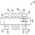
도 1은 기판(102) 상에 형성된 메모리 디바이스(100)를 도시한다. 전하 저장층(들)(112)은 (예를 들어, 현재 알려졌든지 미래에 개발되든지, 터널 유전 층, 폴리실리콘 층, 전하 블로킹층의 조합; 질화물층, 산화물층, 질화물층의 조합; 또는 다른 어떤 다른 층 또는 전하 저장 기능을 제공할 수 있는 층들의 조합) 세장형의 바디 영역(elongated body region)(110)을 둘러싸서 다수의 게이트(114)(또한 세장형의 바디 영역(110) 및 전하 저장층(들)(112)의 각 교차 섹션을 실질적으로 둘러싸는)의 각각에 대응하는 각 전하 구조를 형성한다. 제1 선택 게이트(120)와 제2 선택 게이트(122)가 세장형의 바디 영역(110)을 드레인 영역(132) 및 소스 영역(130)에 각각 선택적으로 전기적으로 연결하기 위해 도시된다. 유전체(104)는 상술한 것과 같은 부품들 사이의 공간을 채울 수 있다.FIG. 1 illustrates a
도 1은 세장형의 바디 영역(110)이 1쌍의 상향 단부를 갖는 "U"자 형상을 형성하는 일 실시예를 도시한다. 다른 예의 구조(도시하지 않음)는 상향하는 하나의 단부와 하향하는 다른 단부를 갖는 선형, 수직의, 세장형의 바디 영역(110)을 포함한다. 다른 예의 구조(도시하지 않음)는 양측에 단부를 갖는 수평, 선형의 세장형의 바디 영역(110)을 포함한다. 실질적으로 "U"자 형상의 구조와 같은 2개의 상향 단부를 갖는 실시예는 부품들이 구조에서 보다 깊게 형성되는 실시예들과 비교할 때 제조 중 세장형의 바디 영역(110)의 단부에서 어떤 부품들을 보다 쉽게 형성할 수 있게 한다.Figure 1 illustrates one embodiment in which
일례에서 세장형의 바디 영역(110)은 p형 반도체 재료로부터 형성된다. 소스 영역(130)과 드레인 영역(132)은 세장형의 바디 영역(110)의 제1 단부(111)와 제2 단부(113)에 각각 연결된다. 일례에서 소스 영역(130)과 드레인 영역은 n+ 폴리실리콘과 같은 n형 반도체 재료를 포함한다. 동작시 세장형의 바디 영역(110), 드레인 영역(132)에의 소스 영역(130)의 경로는 n-p-n 트랜지스터로서 동작하며 선택 게이트(120, 122)와 게이트(114)는 경로를 따라 신호 전송을 허용 또는 금지하도록 동작한다. 도시한 예에서 소스 영역(130), 세장형의 바디 영역(110), 드레인 영역(132), 선택 게이트(120, 122) 및 게이트(114)는 함께 메모리 셀 스트링(101)을 형성한다.In one example, the
소스 라인(126)과 비트 라인(128)과 같은 데이터 라인은 소스 영역(130)과 드레인 영역(132)에 각각 연결된다. 일 실시예에서 플러그(124)가 비트 라인(128)을 드레인 영역(132)에 연결하기 위해 사용된다. 따라서 드레인 영역(132)은 이 실시예에서 비트 라인(128)에 "간접적으로 연결된"으로 서술될 수 있다. 소스 라인(126), 비트 라인(128) 및 플러그(124)는 알루미늄, 구리, 또는 텅스텐과 같은 금속, 또는 이들 또는 다른 도체 금속의 합금을 포함하거나, 알루미늄, 구리, 또는 텅스텐과 같은 금속, 또는 이들 또는 다른 도체 금속의 합금으로 구성되거나, 또는 알루미늄, 구리 또는 텅스텐과 같은 금속, 또는 이들 또는 다른 도체 금속의 합금으로 본질적으로 구성될 수 있다. 본 설명에서 용어 "금속"은 또한 금속 질화물 또는 주로 도체로서 동작하는 다른 재료를 포함한다.Data lines such as
도 2는 도 1로부터의 메모리 셀 스트링(101)의 블록 선도를 도시한다. 일 실시예에서 연결 영역(134)은 소스 영역(130)과 바디 영역(110) 사이에 위치하며 소스 영역(130)과 바디 영역(110)을 연결하기 위해 사용된다. 예를 들어, 연결 영역(134)은 일단부에서 소스 영역(130)에 직접 연결될 수 있으며 타단부에서 바디 영역(110)에 직접 연결될 수 있다. 일 실시예에서 연결 영역(134)은 바디 영역(110)을 형성하기 위해 사용된 반도체 재료의 밴드 갭보다 낮은 밴드 갭을 갖는 반도체 재료를 포함하거나, 바디 영역을 형성하기 위해 사용된 반도체 재료의 밴드 갭보다 낮은 밴드 갭을 갖는 반도체 재료로 구성되거나, 또는 바디 영역을 형성하기 위해 사용된 반도체 재료의 밴드 갭보다 낮은 밴드 갭을 갖는 반도체 재료로 본질적으로 구성될 수 있다. 일례에서 상기 바디 영역은 실리콘을 포함하거나, 실리콘으로 구성되거나, 본질적으로 실리콘으로 구성된다. 일례에서 바디 영역은 p형 실리콘으로부터 형성된다. 실리콘은 약 1.11eV의 밴드 갭을 갖는다.Figure 2 shows a block diagram of the
실리콘보다 낮은 밴드 갭을 갖는 연결 영역(134)을 위한 다수의 예시 재료는 게르마늄(약 0.67eV), 안티몬화갈륨(약 0.7eV), 질화인듐(약 0.7eV), 비화인듐(약 0.36eV), 황화납(약 0.37eV), 셀렌화납(약 0.27eV), 텔루르화납(약 0.29eV) 및 실리콘 게르마늄을 포함한다.(0.67 eV), gallium antimonide (about 0.7 eV), indium nitride (about 0.7 eV), indium indium (about 0.36 eV) , Lead sulfide (about 0.37 eV), tellurium (about 0.27 eV), tellurium (about 0.29 eV), and silicon germanium.
하나 또는 그 이상의 실시예에서 연결 영역(134)은 에피택셜 실리콘 게르마늄을 포함하거나, 에피택셜 실리콘 게르마늄으로 구성되거나, 또는 에피택셜 실리콘 게르마늄으로 본질적으로 구성된다. 실리콘 게르마늄은 조밀 격자 정합과 기존의 실리콘 처리 장치와의 호환성으로 인해 실리콘을 사용하는 용도에 적합하다. 실리콘 게르마늄은 각 부품들의 합금 소수분을 나타내는 x를 포함하여 SixGe1-x로 표현될 수 있다. x가 변함에 따라 실리콘 게르마늄의 밴드 갭은 변한다. 실리콘 게르마늄의 몇 개의 합금 조합은 실리콘보다 낮은 밴드 갭을 보인다. 일례에서 실리콘 게르마늄은 x가 0.2와 0.8 사이인 SixGe1-x를 포함한다. 일례에서 실리콘 게르마늄은 x가 0.4와 0.6 사이인 SixGe1-x를 포함한다. 일례에서 실리콘 게르마늄은 x가 약 0.5인 SixGe1-x를 포함한다.In one or more embodiments, the
연결 영역(134)이 바디 영역의 밴드 갭보다 낮은 밴드 갭을 갖는 실시예들에서, 증가된 게이트 유도 드레인 누설은 연결 영역(134)과 바디 영역(110) 사이의 인터페이스(136)에서 가능하다. 도 2 구성의 게이트 유도 드레인 누설은 단지 반도체 재료가 소스 선택 게이트(122)에 인접하여 존재하는 바디 영역(110)만을 갖는 구성에 비해 증가되었다. 증가된 게이트 유도 드레인 누설은 방향(137)의 바디 영역을 바이어스하도록 바디 영역(110)으로의 더 신뢰성 있는 전하 흐름을 제공한다. 신뢰성 있는 바이어스 전압은 큰 전압차가 사용되는 소거 동작과 같은 다수의 기억 동작에 있어 바람직하다.In embodiments where the
소거 동작을 위해 선택되지 않은 메모리 셀 스트링(101)에서 선택되지 않은 스트링(101)의 바디 영역(110)은 소거되는 것으로부터 선택되지 않은 스트링의 전하 저장 구조를 금지하도록 부스트 동작(boost operation)을 이용하여 바이어스된다. 부스트 동작에서 전압이 게이트(114)에 적용된 전압으로 바디 영역의 용량 결합을 통해 적어도 일부분의 바디 영역(110)에 적용된다. 예를 들어 10볼트가 게이트(114)에 위치하고, 일정 량의 바이어스 전압(예를 들어 약 7볼트)이 결합을 통하여 바디 영역(110)에 전달된다.The
부스트 동작을 이용하여 바디 영역(110) 내에 전하를 유지하는 것은 바람직하다. 결과적으로, 낮은 게이트 유도 드레인 누설이 부스트 동작 중에는 바람직하다. 도 2에서 소스 선택 게이트(122)에 인접한 바디 영역(110)의 연부(138)는 실리콘 또는 연결 영역(134)보다 더 높은 밴드 갭을 갖는 다른 반도체 재료로 형성된다. 부스트 동작 중에 연부(138)에서 방향(139)으로의 게이트 유도 드레인 누설은 소거 동작 중에 인터페이스(136)에서 방향(137)으로의 게이트 유도 드레인 누설에 비해 낮다.It is desirable to maintain charge within the
전술한 바와 같이 다른 밴드 갭의 재료를 갖는 구성을 사용하는 것은 소거 동작 중에 바디 영역(110)의 신뢰성 있는 바이어싱을 제공하며 부스트 동작 중에 바디 영역(110)에 신뢰성 있는 전하 유지를 제공한다.Using a configuration with a material of a different bandgap as described above provides for reliable biasing of the
도 3은 기판(202) 상에 형성된 메모리 디바이스(200)를 도시한다. 전하 저장 층(들)(212)은 실질적으로 세장형의 바디 영역(210)을 실질적으로 둘러싸서 다수의 게이트(214)(또한 세장형의 바디 영역(210)과 전하 저장 층(들)(212)의 각 교차 섹션을 실질적으로 둘러쌈)의 각각에 대응하는 각 전하 구조를 형성한다. 제1 선택 게이트(220)와 제2 선택 게이트(222)가 세장형의 바디 영역(210)을 드레인 영역(232) 및 소스 영역(230)에 각각 선택적으로 연결하기 위해 도시된다. 유전체(204)는 상술한 것들과 같은 부품들 사이의 공간을 채울 수 있다. 도시한 예에서 1 소스 영역(230), 세장형의 바디 영역(210), 드레인 영역(232), 선택 게이트(220), (222) 및 게이트(214)는 함께 메모리 셀 스트링(201)을 형성한다.FIG. 3 shows a
전술한 실시예와 유사하게, 소스 라인(226)과 비트라인(228)은 소스 영역(230)과 드레인 영역(232)에 각각 연결된다. 일 실시예에서 플러그(224)는 비트라인(228)과 드레인 영역(232)을 연결하기 위해 사용된다.The
도 1과 도 2는 바디 영역(110)의 소스 단부에만 위치하는 소스 연결 영역(134)를 갖는 메모리 디바이스(100)의 실시예를 나타낸다. 도 3은 바디 영역(210)을 소스 영역(230)에 결합시키는 소스 연결 영역(234)과 바디 영역(210)을 드레인 영역(232)에 연결하는 드레인 연결 영역(236)을 포함하는 메모리 디바이스(200)를 나타낸다. 도 1 및 도 2의 예 구성에서의 동작과 유사하게, 도 3 및 도 4의 메모리 디바이스(200)는 방향(241) 및 방향(243)으로 제1 게이트 유도 드레인 누설을, 제1 게이트 유도 드레인 누설보다 낮은 방향(242) 및 방향(244)으로 제2 게이트 유도 드레인 누설을 제공한다.Figures 1 and 2 illustrate an embodiment of a
선택된 실시예에서, 드레인 연결 영역(236)의 추가는 또한 메모리 디바이스(200)를 증진시키며, 소거 동작 중 바디 영역(210)의 신뢰할 수 있는 바이어싱을, 또한 부스트 동작 중 바디 영역(210)의 신뢰할 수 있는 전하 유지를 제공한다. 메모리 디바이스(200)의 대략 "U"자 형상의 구성과 같은 메모리 디바이스 구성에서 드레인에 인접한 제2 연결 영역을 형성하는 것은 간단하며 바람직하다. 드레인이 바디 영역 밑에 매립되는 다른 구성은 소스 영역(230)에 인접한 연결 영역(234)과 같은 단일 연결 영역만을 사용한다.In a selected embodiment, the addition of the
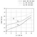
도 5는 소스 선택 게이트가 실리콘 바디 영역(이 시뮬레이션에 대해 밴드 갭이 1.08eV로 추정됨)에만 인접한 게이트 유도 드레인 누설의 시뮬레이션 라인(510)을 도시한다. 라인(512)은 소스 선택 게이트도 0.88eV의 밴드 갭을 갖는 소스 연결 영역에 인접한 전술한 실시예에 따른 구성의 게이트 유도 드레인 누설을 나타낸다. 라인(514)은 소스 선택 게이트도 0.68eV의 밴드 갭을 갖는 소스 연결 영역에 인접한 전술한 실시예에 따른 구성의 게이트 유도 드레인 누설을 나타낸다. 도면으로부터 알 수 있는 바와 같이, 실리콘보다 낮은 밴드 갭을 갖는 연결 영역의 추가는 예를 들어 소거 동작 중 게이트 유도 드레인 누설의 현저한 증가를 제공한다.Figure 5 shows a
도 6에 포함된 컴퓨터와 같은 정보 처리 시스템의 일 실시예는 본 발명의 고 레벨 디바이스 적용의 일 실시예를 나타낸다. 도 6은 전술한 바와 같이 본 발명의 일 실시예에 따른 메모리 디바이스를 내장하는 정보 처리 시스템(600)의 블록 선도다. 정보 처리 시스템(600)은 본 발명의 탈결합(decoupling)이 사용될 수 있는 전자 시스템의 단지 일 실시예이다. 다른 예들은 태블릿 컴퓨터, 카메라, 개인 정보 단말기(PDA), 휴대폰, MP3 플레이어, 비행기, 위성, 군용 차량 등을 포함하지만, 이에 제한되지는 않는다.One embodiment of an information processing system, such as the computer included in Figure 6, represents one embodiment of the high level device application of the present invention. 6 is a block diagram of an
이 예에서, 정보 처리 시스템(600)은 시스템의 다양한 부품들을 연결하기 위한 시스템 버스(602)를 포함하는 데이터 처리 시스템을 포함한다. 시스템 버스(602)는 정보 처리 시스템(600)의 다양한 부품들 중에서 통신 링크를 제공하며 단일 버스, 버스의 조합, 또는 어떤 다른 적당한 방식으로서 이행된다.In this example, the
칩 조립체(604)는 시스템 버스(602)에 연결된다. 칩 조립체(604)는 어떤 회로 또는 회로의 동작적으로 호환성 있는 조합을 포함한다. 일 실시예에서, 칩 조립체(604)는 어떤 형식도 가능한 프로세서(606)를 포함한다. 여기서 사용된 바와 같이, "프로세서"는 마이크로프로세서, 마이크로콘트롤러, 그래픽 프로세서, 디지털 신호 프로세서(DSP), 또는 다른 형식의 프로세서 또는 처리 회로와 같은 어떤 형식의 계산 회로를 의미하지만, 이에 제한되지는 않는다.The
일 실시예에서, 메모리 디바이스(607)는 칩 조립체(604)에 포함된다. 일 실시예에서, 메모리 디바이스(607)는 전술한 실시예에 따른 NAND 메모리 디바이스를 포함한다.In one embodiment,
일 실시예에서, 프로세서 칩이 아닌 추가적인 논리 칩(608)은 칩 조립체(604)에 포함된다. 프로세서 칩이 아닌 논리 칩(608)의 일례는 아날로그-디지털 변환기를 포함한다. 커스텀 회로와 같은 논리 칩(608)상의 다른 회로, 응용 주문형 집적 회로(ASIC) 등도 본 발명의 일 실시예에 포함된다.In one embodiment, an
정보 처리 시스템(600)도 외부 메모리(611)를 포함하며, 그것은 1개 이상의 하드 드라이브(612), 및/또는 컴팩트 디스크(CD), 플래시 드라이브, 디지털 비디오 디스크(DVD) 등과 같은 제거 가능한 미디어(613)를 처리하는 1개 이상의 드라이브와 같은 특정 응용에 적합한 1개 이상의 메모리 요소를 포함할 수 있다. 전술한 예에서 서술된 바와 같이 제조된 반도체 메모리 다이는 정보 처리 시스템(600)에 포함된다.The
정보 처리 시스템(600)은 또한 모니터와 같은 디스플레이 디바이스(609), 스피커 등과 같은 추가적인 주변 부품(610) 및 키보드 및/또는 마우스, 트랙볼, 게임 제어기, 음성-인식 디바이스, 또는 시스템 사용자로 하여금 정보를 정보 처리 시스템(600)에 입력하며 정보 처리 시스템으로부터 정보를 수신할 수 있게 하는 다른 장치를 포함할 수 있는 제어기(614)를 포함한다.The
본 발명의 다수의 실시예들이 서술되었지만 상기한 것들이 철저하게 하고자 한 것은 아니다. 특정한 실시예들이 여기서 서술되고 설명되었지만 당 분야의 기술자들은 동일한 목적을 달성하기 위해 다른 장치들이 특정 실시예들을 대체할 수 있음을 인식할 것이다. 이 출원은 본 발명의 어떤 적용 또는 변형예들도 커버하려 한다. 상기 설명이 설명을 위한 것이며 제한적이 아님이 이해될 것이다. 상기 실시예들과 다른 실시예들의 조합은 상기 설명들을 학습함으로써 당 분야의 기술자들에게는 명백할 것이다.Although a number of embodiments of the present invention have been described, the foregoing is not intended to be exhaustive. Although specific embodiments have been described and illustrated herein, those skilled in the art will recognize that other devices may be substituted for specific embodiments to achieve the same purpose. This application is intended to cover any adaptations or variations of the present invention. It is to be understood that the above description is intended to be illustrative and not restrictive. Combinations of the above embodiments and other embodiments will be apparent to those skilled in the art by learning from the above description.
Claims (27)
Translated fromKorean제1 밴드 갭을 갖는 반도체를 포함하는 바디 영역;
상기 바디 영역의 제1 단부에 연결된 소스 영역과, 상기 바디 영역의 제2 단부에 연결된 드레인 영역;
각각이 상기 바디 영역으로부터 적어도 각 전하 저장 구조만큼 분리되어 있으며, 상기 바디 영역의 길이를 따르는 복수의 게이트;
상기 제1 밴드 갭보다 낮은 제2 밴드 갭을 갖는 반도체를 포함하며 상기 소스 영역을 상기 바디 영역에 결합시키는 연결 영역: 및
상기 바디 영역과 상기 연결 영역에 인접한 소스 선택 게이트를 포함하는 메모리 디바이스.13. A memory device comprising:
A body region comprising a semiconductor having a first bandgap;
A source region coupled to a first end of the body region; a drain region coupled to a second end of the body region;
Each of the plurality of gates being separated from the body region by at least respective charge storage structures, the gates being along the length of the body region;
A junction region comprising a semiconductor having a second bandgap lower than the first bandgap and coupling the source region to the body region; and
And a source select gate adjacent the body region and the connection region.
제1 밴드 갭보다 낮은 밴드 갭을 갖는 반도체를 포함하며 상기 드레인 영역을 상기 바디 영역에 결합시키는 드레인 연결 영역; 및
상기 바디 영역과 상기 드레인 연결 영역에 인접한 드레인 선택 게이트를 더 포함하는 메모리 디바이스.2. The apparatus of claim 1, wherein the connection region comprises a source connection region,
A drain connection region including a semiconductor having a band gap lower than the first band gap and coupling the drain region to the body region; And
And a drain select gate adjacent the body region and the drain connection region.
메모리 셀 스트링을 포함하되, 상기 메모리 셀 스트링은
제1 밴드 갭을 갖는 반도체를 포함하며, 제1 상향 단부와 제2 상향 단부를 갖는 바디 영역;
상기 제1 상향 단부에 연결된 드레인 영역;
상기 제2 상향 단부에 연결된 소스 영역;
상기 바디 영역의 길이를 따른 복수의 게이트;
제1 밴드 갭보다 낮은 제2 밴드 갭을 갖는 반도체를 포함하며 상기 소스 영역을 상기 바디 영역에 결합시키는 연결 영역;
상기 바디 영역과 상기 연결 영역에 인접한 소스 선택 게이트; 및
상기 드레인 영역에 연결된 데이터 라인; 및
상기 소스 영역에 연결된 소스 라인을 포함하는 것인 메모리 디바이스.13. A memory device comprising:
And a memory cell string, wherein the memory cell string
A body region comprising a semiconductor having a first bandgap, the body region having a first upper end and a second upper end;
A drain region coupled to the first upper end;
A source region coupled to the second upper end;
A plurality of gates along the length of the body region;
A connection region including a semiconductor having a second band gap lower than the first band gap and coupling the source region to the body region;
A source select gate adjacent said body region and said connection region; And
A data line coupled to the drain region; And
And a source line coupled to the source region.
Applications Claiming Priority (3)
| Application Number | Priority Date | Filing Date | Title |
|---|---|---|---|
| US13/020,337 | 2011-02-03 | ||
| US13/020,337US8431961B2 (en) | 2011-02-03 | 2011-02-03 | Memory devices with a connecting region having a band gap lower than a band gap of a body region |
| PCT/US2012/023499WO2012106439A2 (en) | 2011-02-03 | 2012-02-01 | Memory devices with a connecting region having a band gap lower than a band gap of a body region |
Publications (2)
| Publication Number | Publication Date |
|---|---|
| KR20140052946A KR20140052946A (en) | 2014-05-07 |
| KR101774960B1true KR101774960B1 (en) | 2017-09-05 |
Family
ID=46600064
Family Applications (1)
| Application Number | Title | Priority Date | Filing Date |
|---|---|---|---|
| KR1020137023223AActiveKR101774960B1 (en) | 2011-02-03 | 2012-02-01 | Memory devices with a connecting region having a band gap lower than a band gap of a body region |
Country Status (6)
| Country | Link |
|---|---|
| US (4) | US8431961B2 (en) |
| JP (1) | JP5793576B2 (en) |
| KR (1) | KR101774960B1 (en) |
| CN (1) | CN103339728B (en) |
| TW (1) | TWI523201B (en) |
| WO (1) | WO2012106439A2 (en) |
Families Citing this family (13)
| Publication number | Priority date | Publication date | Assignee | Title |
|---|---|---|---|---|
| KR20120069034A (en)* | 2010-12-20 | 2012-06-28 | 삼성전자주식회사 | Vertical memory devices and methods of manufacturing the same |
| US8750040B2 (en) | 2011-01-21 | 2014-06-10 | Micron Technology, Inc. | Memory devices having source lines directly coupled to body regions and methods |
| US8431961B2 (en) | 2011-02-03 | 2013-04-30 | Micron Technology, Inc. | Memory devices with a connecting region having a band gap lower than a band gap of a body region |
| US9214235B2 (en)* | 2013-04-16 | 2015-12-15 | Conversant Intellectual Property Management Inc. | U-shaped common-body type cell string |
| JP6403558B2 (en)* | 2014-03-28 | 2018-10-10 | 大阪瓦斯株式会社 | Power generator |
| US9893076B2 (en)* | 2015-02-05 | 2018-02-13 | Conversant Intellectual Property Management Inc. | Access transistor of a nonvolatile memory device and method for fabricating same |
| US9761599B2 (en) | 2015-08-17 | 2017-09-12 | Micron Technology, Inc. | Integrated structures containing vertically-stacked memory cells |
| US10608012B2 (en) | 2017-08-29 | 2020-03-31 | Micron Technology, Inc. | Memory devices including memory cells and related methods |
| EP3676873A4 (en) | 2017-08-29 | 2021-05-26 | Micron Technology, Inc. | DEVICES AND SYSTEMS INCLUDING STRING DRIVERS WITH HIGH GAP MATERIAL AND METHODS OF FORMING |
| US10923493B2 (en) | 2018-09-06 | 2021-02-16 | Micron Technology, Inc. | Microelectronic devices, electronic systems, and related methods |
| WO2020076652A1 (en) | 2018-10-09 | 2020-04-16 | Micron Technology, Inc. | Semiconductor devices comprising transistors having increased threshold voltage and related methods and systems |
| KR102723994B1 (en) | 2019-02-27 | 2024-10-30 | 삼성전자주식회사 | Integrated circuit devices |
| US11869590B2 (en)* | 2021-08-27 | 2024-01-09 | Micron Technology, Inc. | Memory devices including gate leakage transistors |
Citations (3)
| Publication number | Priority date | Publication date | Assignee | Title |
|---|---|---|---|---|
| US6013928A (en) | 1991-08-23 | 2000-01-11 | Semiconductor Energy Laboratory Co., Ltd. | Semiconductor device having interlayer insulating film and method for forming the same |
| US20040157353A1 (en) | 2001-03-13 | 2004-08-12 | International Business Machines Corporation | Ultra scalable high speed heterojunction vertical n-channel MISFETs and methods thereof |
| JP2010199312A (en) | 2009-02-25 | 2010-09-09 | Toshiba Corp | Non-volatile semiconductor memory device and method for manufacturing the same |
Family Cites Families (37)
| Publication number | Priority date | Publication date | Assignee | Title |
|---|---|---|---|---|
| US7253437B2 (en)* | 1990-12-25 | 2007-08-07 | Semiconductor Energy Laboratory Co., Ltd. | Display device having a thin film transistor |
| US5581092A (en)* | 1993-09-07 | 1996-12-03 | Semiconductor Energy Laboratory Co., Ltd. | Gate insulated semiconductor device |
| JPH08148669A (en) | 1994-11-22 | 1996-06-07 | Sanyo Electric Co Ltd | Semiconductor device |
| US6313487B1 (en) | 2000-06-15 | 2001-11-06 | Board Of Regents, The University Of Texas System | Vertical channel floating gate transistor having silicon germanium channel layer |
| CN101807588A (en)* | 2004-07-30 | 2010-08-18 | 株式会社半导体能源研究所 | Semiconductor device |
| JP4822841B2 (en)* | 2005-12-28 | 2011-11-24 | 株式会社東芝 | Semiconductor memory device and manufacturing method thereof |
| TWI416738B (en) | 2006-03-21 | 2013-11-21 | Semiconductor Energy Lab | Nonvolatile semiconductor memory device |
| US7554854B2 (en) | 2006-03-31 | 2009-06-30 | Semiconductor Energy Laboratory Co., Ltd. | Method for deleting data from NAND type nonvolatile memory |
| US7646039B2 (en)* | 2007-07-31 | 2010-01-12 | International Business Machines Corporation | SOI field effect transistor having asymmetric junction leakage |
| US7936042B2 (en)* | 2007-11-13 | 2011-05-03 | International Business Machines Corporation | Field effect transistor containing a wide band gap semiconductor material in a drain |
| EP2120266B1 (en)* | 2008-05-13 | 2015-10-28 | Imec | Scalable quantum well device and method for manufacturing the same |
| JP6053250B2 (en)* | 2008-06-12 | 2016-12-27 | ピーエスフォー ルクスコ エスエイアールエルPS4 Luxco S.a.r.l. | Semiconductor device |
| KR101502584B1 (en)* | 2008-10-16 | 2015-03-17 | 삼성전자주식회사 | Nonvolatile memory device |
| US8067803B2 (en)* | 2008-10-16 | 2011-11-29 | Micron Technology, Inc. | Memory devices, transistor devices and related methods |
| JP5364342B2 (en)* | 2008-11-10 | 2013-12-11 | 株式会社東芝 | Nonvolatile semiconductor memory device and manufacturing method thereof |
| US8213226B2 (en)* | 2008-12-05 | 2012-07-03 | Micron Technology, Inc. | Vertical transistor memory cell and array |
| KR101527192B1 (en)* | 2008-12-10 | 2015-06-10 | 삼성전자주식회사 | Nonvolatile memory device and manufacturing method thereof |
| JP5275052B2 (en)* | 2009-01-08 | 2013-08-28 | 株式会社東芝 | Nonvolatile semiconductor memory device |
| US8405121B2 (en)* | 2009-02-12 | 2013-03-26 | Infineon Technologies Ag | Semiconductor devices |
| JP5397674B2 (en) | 2009-02-19 | 2014-01-22 | 東芝ライテック株式会社 | Lamp apparatus and lighting apparatus |
| JP2010199235A (en)* | 2009-02-24 | 2010-09-09 | Toshiba Corp | Nonvolatile semiconductor storage device |
| JP5104782B2 (en) | 2009-02-25 | 2012-12-19 | 富士電機株式会社 | Thin-film light conversion element manufacturing apparatus and manufacturing method |
| JP2011035237A (en)* | 2009-08-04 | 2011-02-17 | Toshiba Corp | Method of manufacturing semiconductor device, and semiconductor device |
| JP5259552B2 (en)* | 2009-11-02 | 2013-08-07 | 株式会社東芝 | Nonvolatile semiconductor memory device and driving method thereof |
| JP2011198806A (en)* | 2010-03-17 | 2011-10-06 | Toshiba Corp | Semiconductor memory device and method for manufacturing the same |
| JP5072995B2 (en)* | 2010-03-24 | 2012-11-14 | 株式会社東芝 | Nonvolatile semiconductor memory device |
| JP5502629B2 (en)* | 2010-07-12 | 2014-05-28 | 株式会社東芝 | Nonvolatile semiconductor memory device and manufacturing method thereof |
| US8514620B2 (en)* | 2010-11-29 | 2013-08-20 | Micron Technology, Inc. | Memory devices having select gates with P type bodies, memory strings having separate source lines and methods |
| US8750040B2 (en)* | 2011-01-21 | 2014-06-10 | Micron Technology, Inc. | Memory devices having source lines directly coupled to body regions and methods |
| US8431961B2 (en) | 2011-02-03 | 2013-04-30 | Micron Technology, Inc. | Memory devices with a connecting region having a band gap lower than a band gap of a body region |
| KR20120131688A (en) | 2011-05-26 | 2012-12-05 | 에스케이하이닉스 주식회사 | Nonvolatile memory device and method for fabricating the same |
| US8933502B2 (en)* | 2011-11-21 | 2015-01-13 | Sandisk Technologies Inc. | 3D non-volatile memory with metal silicide interconnect |
| US8917557B2 (en)* | 2011-12-15 | 2014-12-23 | Kabushiki Kaisha Toshiba | Nonvolatile semiconductor memory device |
| US8865535B2 (en)* | 2012-04-13 | 2014-10-21 | Sandisk Technologies Inc. | Fabricating 3D non-volatile storage with transistor decoding structure |
| US9214235B2 (en)* | 2013-04-16 | 2015-12-15 | Conversant Intellectual Property Management Inc. | U-shaped common-body type cell string |
| US9240420B2 (en)* | 2013-09-06 | 2016-01-19 | Sandisk Technologies Inc. | 3D non-volatile storage with wide band gap transistor decoder |
| US9105468B2 (en)* | 2013-09-06 | 2015-08-11 | Sandisk 3D Llc | Vertical bit line wide band gap TFT decoder |
- 2011
- 2011-02-03USUS13/020,337patent/US8431961B2/enactiveActive
- 2012
- 2012-02-01KRKR1020137023223Apatent/KR101774960B1/enactiveActive
- 2012-02-01JPJP2013552601Apatent/JP5793576B2/enactiveActive
- 2012-02-01WOPCT/US2012/023499patent/WO2012106439A2/enactiveApplication Filing
- 2012-02-01CNCN201280007365.6Apatent/CN103339728B/enactiveActive
- 2012-02-03TWTW101103566Apatent/TWI523201B/enactive
- 2013
- 2013-04-29USUS13/872,762patent/US8766320B2/enactiveActive
- 2014
- 2014-06-30USUS14/320,174patent/US9640260B2/enactiveActive
- 2017
- 2017-05-01USUS15/583,411patent/US9953710B2/enactiveActive
Patent Citations (3)
| Publication number | Priority date | Publication date | Assignee | Title |
|---|---|---|---|---|
| US6013928A (en) | 1991-08-23 | 2000-01-11 | Semiconductor Energy Laboratory Co., Ltd. | Semiconductor device having interlayer insulating film and method for forming the same |
| US20040157353A1 (en) | 2001-03-13 | 2004-08-12 | International Business Machines Corporation | Ultra scalable high speed heterojunction vertical n-channel MISFETs and methods thereof |
| JP2010199312A (en) | 2009-02-25 | 2010-09-09 | Toshiba Corp | Non-volatile semiconductor memory device and method for manufacturing the same |
Also Published As
| Publication number | Publication date |
|---|---|
| US20130234206A1 (en) | 2013-09-12 |
| CN103339728B (en) | 2015-11-25 |
| TW201234567A (en) | 2012-08-16 |
| US9640260B2 (en) | 2017-05-02 |
| JP2014504810A (en) | 2014-02-24 |
| WO2012106439A2 (en) | 2012-08-09 |
| US20140313833A1 (en) | 2014-10-23 |
| TWI523201B (en) | 2016-02-21 |
| JP5793576B2 (en) | 2015-10-14 |
| US8766320B2 (en) | 2014-07-01 |
| US20170236589A1 (en) | 2017-08-17 |
| CN103339728A (en) | 2013-10-02 |
| US9953710B2 (en) | 2018-04-24 |
| WO2012106439A3 (en) | 2012-10-11 |
| US8431961B2 (en) | 2013-04-30 |
| US20120199877A1 (en) | 2012-08-09 |
| KR20140052946A (en) | 2014-05-07 |
Similar Documents
| Publication | Publication Date | Title |
|---|---|---|
| KR101774960B1 (en) | Memory devices with a connecting region having a band gap lower than a band gap of a body region | |
| US9761712B1 (en) | Vertical transistors with merged active area regions | |
| US12062396B2 (en) | Memory devices having source lines directly coupled to body regions and methods | |
| TWI475647B (en) | Memory devices having select gates with p type bodies, memory strings having separate source lines and methods | |
| US9190472B2 (en) | Apparatuses and methods comprising a channel region having different minority carrier lifetimes |
Legal Events
| Date | Code | Title | Description |
|---|---|---|---|
| PA0105 | International application | St.27 status event code:A-0-1-A10-A15-nap-PA0105 | |
| PG1501 | Laying open of application | St.27 status event code:A-1-1-Q10-Q12-nap-PG1501 | |
| A201 | Request for examination | ||
| A302 | Request for accelerated examination | ||
| PA0201 | Request for examination | St.27 status event code:A-1-2-D10-D11-exm-PA0201 | |
| PA0302 | Request for accelerated examination | St.27 status event code:A-1-2-D10-D17-exm-PA0302 St.27 status event code:A-1-2-D10-D16-exm-PA0302 | |
| E902 | Notification of reason for refusal | ||
| PE0902 | Notice of grounds for rejection | St.27 status event code:A-1-2-D10-D21-exm-PE0902 | |
| P11-X000 | Amendment of application requested | St.27 status event code:A-2-2-P10-P11-nap-X000 | |
| P13-X000 | Application amended | St.27 status event code:A-2-2-P10-P13-nap-X000 | |
| E701 | Decision to grant or registration of patent right | ||
| PE0701 | Decision of registration | St.27 status event code:A-1-2-D10-D22-exm-PE0701 | |
| PR0701 | Registration of establishment | St.27 status event code:A-2-4-F10-F11-exm-PR0701 | |
| PR1002 | Payment of registration fee | St.27 status event code:A-2-2-U10-U12-oth-PR1002 Fee payment year number:1 | |
| PG1601 | Publication of registration | St.27 status event code:A-4-4-Q10-Q13-nap-PG1601 | |
| PR1001 | Payment of annual fee | St.27 status event code:A-4-4-U10-U11-oth-PR1001 Fee payment year number:4 | |
| PR1001 | Payment of annual fee | St.27 status event code:A-4-4-U10-U11-oth-PR1001 Fee payment year number:5 | |
| PR1001 | Payment of annual fee | St.27 status event code:A-4-4-U10-U11-oth-PR1001 Fee payment year number:6 | |
| P22-X000 | Classification modified | St.27 status event code:A-4-4-P10-P22-nap-X000 | |
| P22-X000 | Classification modified | St.27 status event code:A-4-4-P10-P22-nap-X000 | |
| PR1001 | Payment of annual fee | St.27 status event code:A-4-4-U10-U11-oth-PR1001 Fee payment year number:7 | |
| PR1001 | Payment of annual fee | St.27 status event code:A-4-4-U10-U11-oth-PR1001 Fee payment year number:8 | |
| P22-X000 | Classification modified | St.27 status event code:A-4-4-P10-P22-nap-X000 | |
| PR1001 | Payment of annual fee | St.27 status event code:A-4-4-U10-U11-oth-PR1001 Fee payment year number:9 |