KR101772567B1 - Nonvolatile memory device, erasing method thereof and memory system including the same - Google Patents
Nonvolatile memory device, erasing method thereof and memory system including the sameDownload PDFInfo
- Publication number
- KR101772567B1 KR101772567B1KR1020110015687AKR20110015687AKR101772567B1KR 101772567 B1KR101772567 B1KR 101772567B1KR 1020110015687 AKR1020110015687 AKR 1020110015687AKR 20110015687 AKR20110015687 AKR 20110015687AKR 101772567 B1KR101772567 B1KR 101772567B1
- Authority
- KR
- South Korea
- Prior art keywords
- substrate
- voltage
- ground
- string
- memory
- Prior art date
- Legal status (The legal status is an assumption and is not a legal conclusion. Google has not performed a legal analysis and makes no representation as to the accuracy of the status listed.)
- Active
Links
Images


Classifications
- G—PHYSICS
- G11—INFORMATION STORAGE
- G11C—STATIC STORES
- G11C16/00—Erasable programmable read-only memories
- G11C16/02—Erasable programmable read-only memories electrically programmable
- G11C16/06—Auxiliary circuits, e.g. for writing into memory
- G11C16/10—Programming or data input circuits
- G11C16/14—Circuits for erasing electrically, e.g. erase voltage switching circuits
- G—PHYSICS
- G11—INFORMATION STORAGE
- G11C—STATIC STORES
- G11C16/00—Erasable programmable read-only memories
- G11C16/02—Erasable programmable read-only memories electrically programmable
- G11C16/04—Erasable programmable read-only memories electrically programmable using variable threshold transistors, e.g. FAMOS
- G11C16/0483—Erasable programmable read-only memories electrically programmable using variable threshold transistors, e.g. FAMOS comprising cells having several storage transistors connected in series
- G—PHYSICS
- G11—INFORMATION STORAGE
- G11C—STATIC STORES
- G11C16/00—Erasable programmable read-only memories
- G11C16/02—Erasable programmable read-only memories electrically programmable
- G11C16/06—Auxiliary circuits, e.g. for writing into memory
- G11C16/08—Address circuits; Decoders; Word-line control circuits
- G—PHYSICS
- G11—INFORMATION STORAGE
- G11C—STATIC STORES
- G11C16/00—Erasable programmable read-only memories
- G11C16/02—Erasable programmable read-only memories electrically programmable
- G11C16/06—Auxiliary circuits, e.g. for writing into memory
- G11C16/10—Programming or data input circuits
- G11C16/14—Circuits for erasing electrically, e.g. erase voltage switching circuits
- G11C16/16—Circuits for erasing electrically, e.g. erase voltage switching circuits for erasing blocks, e.g. arrays, words, groups
- H—ELECTRICITY
- H10—SEMICONDUCTOR DEVICES; ELECTRIC SOLID-STATE DEVICES NOT OTHERWISE PROVIDED FOR
- H10B—ELECTRONIC MEMORY DEVICES
- H10B43/00—EEPROM devices comprising charge-trapping gate insulators
- H10B43/20—EEPROM devices comprising charge-trapping gate insulators characterised by three-dimensional arrangements, e.g. with cells on different height levels
- H10B43/23—EEPROM devices comprising charge-trapping gate insulators characterised by three-dimensional arrangements, e.g. with cells on different height levels with source and drain on different levels, e.g. with sloping channels
- H10B43/27—EEPROM devices comprising charge-trapping gate insulators characterised by three-dimensional arrangements, e.g. with cells on different height levels with source and drain on different levels, e.g. with sloping channels the channels comprising vertical portions, e.g. U-shaped channels
- H—ELECTRICITY
- H10—SEMICONDUCTOR DEVICES; ELECTRIC SOLID-STATE DEVICES NOT OTHERWISE PROVIDED FOR
- H10B—ELECTRONIC MEMORY DEVICES
- H10B43/00—EEPROM devices comprising charge-trapping gate insulators
- H10B43/30—EEPROM devices comprising charge-trapping gate insulators characterised by the memory core region
- H10B43/35—EEPROM devices comprising charge-trapping gate insulators characterised by the memory core region with cell select transistors, e.g. NAND
Landscapes
- Engineering & Computer Science (AREA)
- Microelectronics & Electronic Packaging (AREA)
- Read Only Memory (AREA)
- Semiconductor Memories (AREA)
- Non-Volatile Memory (AREA)
Abstract
Translated fromKoreanDescription
Translated fromKorean본 발명은 반도체 메모리에 관한 것으로, 더 상세하게는 불휘발성 메모리 장치, 그것의 소거 방법, 그리고 그것을 포함하는 메모리 시스템에 관한 것이다.The present invention relates to semiconductor memory, and more particularly, to a non-volatile memory device, a method of erasing the same, and a memory system including the same.
반도체 메모리 장치(semiconductor memory device)는 실리콘(Si, silicon), 게르마늄(Ge, Germanium), 비화 갈륨(GaAs, gallium arsenide), 인화인듐(InP, indium phospide) 등과 같은 반도체를 이용하여 구현되는 기억장치이다. 반도체 메모리 장치는 크게 휘발성 메모리 장치(Volatile memory device)와 불휘발성 메모리 장치(Nonvolatile memory device)로 구분된다.A semiconductor memory device is a memory device implemented using semiconductors such as silicon (Si), germanium (Ge), gallium arsenide (GaAs), indium phosphide (InP) to be. Semiconductor memory devices are classified into a volatile memory device and a nonvolatile memory device.
휘발성 메모리 장치는 전원 공급이 차단되면 저장하고 있던 데이터가 소멸되는 메모리 장치이다. 휘발성 메모리 장치에는 SRAM (Static RAM), DRAM (Dynamic RAM), SDRAM (Synchronous DRAM) 등이 있다. 불휘발성 메모리 장치는 전원 공급이 차단되어도 저장하고 있던 데이터를 유지하는 메모리 장치이다. 불휘발성 메모리 장치에는 ROM (Read Only Memory), PROM (Programmable ROM), EPROM (Electrically Programmable ROM), EEPROM (Electrically Erasable and Programmable ROM), 플래시 메모리 장치, PRAM (Phase-change RAM), MRAM (Magnetic RAM), RRAM (Resistive RAM), FRAM (Ferroelectric RAM) 등이 있다. 플래시 메모리 장치는 크게 노어 타입과 낸드 타입으로 구분된다.The volatile memory device is a memory device in which data stored in the volatile memory device is lost when power supply is interrupted. Volatile memory devices include static RAM (SRAM), dynamic RAM (DRAM), and synchronous DRAM (SDRAM). A nonvolatile memory device is a memory device that retains data that has been stored even when power is turned off. A nonvolatile memory device includes a ROM (Read Only Memory), a PROM (Programmable ROM), an EPROM (Electrically Programmable ROM), an EEPROM (Electrically Erasable and Programmable ROM), a flash memory device, a PRAM ), RRAM (Resistive RAM), and FRAM (Ferroelectric RAM). Flash memory devices are largely divided into NOR type and NAND type.
본 발명의 목적은 향상된 신뢰성을 갖고 3차원 어레이 구조를 갖는 불휘발성 메모리 장치, 그것의 소거 방법, 그리고 그것을 포함하는 메모리 시스템을 제공하는 데에 있다.An object of the present invention is to provide a nonvolatile memory device having a three-dimensional array structure with improved reliability, an erasing method thereof, and a memory system including the same.
복수의 메모리 셀들, 스트링 선택 트랜지스터, 그리고 접지 선택 트랜지스터를 구비한 메모리 스트링을 포함하는 본 발명의 실시 예에 따른 불휘발성 메모리 장치의 소거 방법은, 상기 복수의 메모리 셀들에 연결된 복수의 워드 라인들에 워드 라인들에 워드 라인 소거 전압을 인가하는 단계; 상기 접지 선택 트랜지스터에 연결된 접지 선택 라인에 특정 전압을 인가하는 단계; 상기 접지 선택 라인에 상기 특정 전압을 인가하는 단계 동안 상기 메모리 셀 스트링이 형성된 기판에 소거 전압을 인가하는 단계; 그리고 상기 기판의 전압 변화에 따라 상기 접지 선택 라인을 플로팅하는 단계를 포함한다.A method for erasing a non-volatile memory device according to an embodiment of the present invention, including a memory string having a plurality of memory cells, a string select transistor, and a ground select transistor, includes the steps of: Applying a word line erase voltage to the word lines; Applying a specific voltage to a ground selection line coupled to the ground selection transistor; Applying an erase voltage to the substrate on which the memory cell string is formed during the step of applying the specific voltage to the ground selection line; And floating the ground selection line according to a change in the voltage of the substrate.
실시 예로서, 상기 특정 전압을 인가하는 단계는 상기 접지 선택 라인에 접지 전압을 인가하는 단계를 포함한다.As an embodiment, applying the specific voltage includes applying a ground voltage to the ground selection line.
실시 예로서, 상기 접지 선택 라인을 플로팅하는 단계는 상기 기판의 전압 레벨이 목표 전압 레벨에 도달할 때 수행된다.As an embodiment, floating the ground selection line is performed when the voltage level of the substrate reaches a target voltage level.
실시 예로서, 상기 복수의 메모리 셀들은 상기 기판과 수직한 방향으로 적층된다.In an embodiment, the plurality of memory cells are stacked in a direction perpendicular to the substrate.
본 발명의 실시 예에 따른 불휘발성 메모리 장치는, 기판 상에 제공되는 복수의 메모리 셀 스트링들을 포함하는 메모리 셀 어레이; 비트 라인들을 통해 상기 복수의 메모리 셀 스트링들과 연결되고, 상기 비트 라인들을 구동하도록 구성되는 읽기 및 쓰기 회로; 복수의 워드 라인들,스트링 선택 라인, 그리고 접지 선택 라인을 통해 상기 복수의 메모리 셀 스트링들에 연결되고, 상기 복수의 워드 라인들 및 상기 선택 라인들을 구동하도록 구성되는 어드레스 디코더; 그리고 소거 동작 시에, 상기 기판의 전압 레벨을 모니터하도록 구성되는 기판 모니터 회로를 포함하고, 소거 동작 시에, 상기 어드레스 디코더는 상기 모니터 결과에 따라 상기 접지 선택 라인을 구동하도록 구성된다.A nonvolatile memory device according to an embodiment of the present invention includes: a memory cell array including a plurality of memory cell strings provided on a substrate; A read and write circuit coupled to the plurality of memory cell strings via bit lines and configured to drive the bit lines; An address decoder coupled to the plurality of memory cell strings via a plurality of word lines, a string select line, and a ground select line, the address decoder configured to drive the plurality of word lines and the select lines; And a substrate monitor circuit configured to monitor a voltage level of the substrate during an erase operation, wherein, in an erase operation, the address decoder is configured to drive the ground select line according to the monitor result.
실시 예로서, 상기 소거 동작의 소거 전압이 상기 기판에 인가되기 시작할 때, 상기 어드레스 디코더는 상기 선택 라인들을 접지 전압으로 구동하도록 구성된다.As an embodiment, when the erase voltage of the erase operation begins to be applied to the substrate, the address decoder is configured to drive the select lines to a ground voltage.
실시 예로서, 상기 소거 동작 시에, 상기 기판의 전압 레벨이 목표 전압 레벨에 도달할 때, 상기 어드레스 디코더는 상기 접지 선택 라인을 플로팅하도록 구성된다.As an embodiment, in the erase operation, the address decoder is configured to plot the ground selection line when the voltage level of the substrate reaches a target voltage level.
실시 예로서, 상기 기판 모니터 회로는 상기 기판의 전압이 제공되는 기판 노드 및 접지 노드 사이에 연결되는 제 1 및 제 2 트림기들; 그리고 상기 제 1 및 제 2 트림기들 사이의 노드의 전압 및 목표 전압을 비교하여, 상기 모니터 결과로 출력하는 비교기를 포함한다.In an embodiment, the substrate monitor circuit includes first and second trimers connected between a substrate node and a ground node to which the voltage of the substrate is provided; And a comparator for comparing the voltage of the node between the first and second trimmers and the target voltage and outputting the result as the monitor result.
본 발명의 실시 예에 따른 불휘발성 메모리 장치의 소거 방법은, 제 1 도전형의 기판에 수직하고, 상기 기판에 접촉하는 상기 제 1 도전형의 필라 활성 바디를 사용하는 스트링 선택 트랜지스터와 복수의 메모리 셀들과 그리고 접지 선택 트랜지스터를 포함하는 메모리 스트링을 포함하는 불휘발성 메모리 장치를 제공하는 단계; 상기 복수의 메모리 셀들에 연결된 복수의 워드 라인들에 워드 라인 소거 전압을 인가하는 단계; 상기 접지 선택 트랜지스터에 연결된 접지 선택 라인에 전압을 인가하는 단계; 상기 기판에 소거 전압을 인가하는 단계; 그리고 상기 기판의 전압 변화에 응답하여 상기 접지 선택 라인을 플로팅하는 단계를 포함한다.A method of erasing a nonvolatile memory device according to an embodiment of the present invention is a method for erasing a nonvolatile memory device including a string selection transistor which is perpendicular to a substrate of a first conductivity type and uses the pillar active body of the first conductivity type, Providing a non-volatile memory device comprising cells and a memory string including a ground selection transistor; Applying a word line erase voltage to a plurality of word lines coupled to the plurality of memory cells; Applying a voltage to a ground select line coupled to the ground select transistor; Applying an erase voltage to the substrate; And floating the ground selection line in response to a change in the voltage of the substrate.
본 발명에 의하면, 접지 선택 트랜지스터의 활성화에 의한 소거 교란이 방지된다. 따라서, 향상된 신뢰성을 갖는 불휘발성 메모리 장치, 그것의 소거 방법, 그리고 그것을 포함하는 메모리 시스템이 제공된다.According to the present invention, erasing disturbance due to activation of the ground selection transistor is prevented. Therefore, a nonvolatile memory device with improved reliability, a method of erasing the same, and a memory system including the same are provided.
도 1은 본 발명의 제 1 실시 예에 따른 불휘발성 메모리 장치를 보여주는 블록도이다.
도 2는 도 1의 메모리 셀 어레이를 보여주는 블록도이다. 도 2를 참조하면, 메모리 셀 어레이는 복수의 메모리 블록들을 포함한다.
도 3은 도 2의 메모리 블록들 중 하나의 제 1 실시 예를 보여주는 사시도이다.
도 4는 도 3의 메모리 블록의 Ⅰ-Ⅰ'선에 따른 단면도이다.
도 5는 도 4의 트랜지스터 구조를 보여주는 단면도이다.
도 6은 도 3 내지 도 5를 참조하여 설명된 메모리 블록의 등가 회로를 보여주는 회로도이다.
도 7은 도 1의 불휘발성 메모리 장치의 소거 동작 시의 전압 조건의 실시 예를 보여주는 테이블이다.
도 8은 도 3 내지 도 6을 참조하여 설명된 메모리 블록의 낸드 스트링들 중 하나를 보여주는 단면도이다.
도 9는 도 1의 불휘발성 메모리 장치의 소거 방법을 보여주는 순서도이다.
도 10은 도 9의 소거 방법에 따른 소거 전압 조건을 보여주는 테이블이다.
도 11은 도 9의 소거 방법 및 도 10의 전압 조건에 따른 전압 변화를 보여주는 타이밍도이다.
도 12는 도 1의 기판 모니터 회로를 보여주는 블록도이다.
도 13은 도 12의 업-트림기를 보여주는 회로도이다.
도 14A는 도 1의 불휘발성 메모리 장치의 메모리 셀 어레이 및 어드레스 디코더를 보여주는 블록도이다.
도 14B는 도 1의 불휘발성 메모리 장치의 메모리 셀 어레이 및 어드레스 디코더의 다른 예를 보여주는 블록도이다.
도 15는 도 3 내지 도 5를 참조하여 설명된 메모리 블록의 등가 회로의 제 1 응용 예를 보여주는 회로도이다.
도 16은 도 3 내지 도 5을 참조하여 설명된 메모리 블록의 등가 회로의 제 2 응용 예를 보여주는 회로도이다.
도 17은 도 3 내지 도 5를 참조하여 설명된 메모리 블록의 등가 회로의 제 3 응용 예를 보여주는 회로도이다.
도 18은 도 3 내지 도 5를 참조하여 설명된 메모리 블록의 등가 회로의 제 4 응용 예를 보여주는 회로도이다.
도 19는 도 3 내지 도 5를 참조하여 설명된 메모리 블록의 등가 회로의 제 5 응용 예를 보여주는 회로도이다.
도 20은 도 3 내지 도 5를 참조하여 설명된 메모리 블록의 등가 회로의 제 6 응용 예를 보여주는 회로도이다.
도 21은 도 3 내지 도 5를 참조하여 설명된 메모리 블록의 등가 회로의 제 7 응용 예를 보여주는 회로도이다.
도 22는 도 2의 메모리 블록의 다른 실시 예를 보여주는 블록도이다.
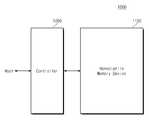
도 23은 도 1의 불휘발성 메모리 장치를 포함하는 메모리 시스템을 보여주는 사시도이다.
도 24는 도 23의 메모리 시스템의 응용 예를 보여주는 블록도이다.
도 25는 도 24를 참조하여 설명된 메모리 시스템을 포함하는 컴퓨팅 시스템을 보여주는 블록도이다.1 is a block diagram showing a nonvolatile memory device according to a first embodiment of the present invention.
2 is a block diagram showing the memory cell array of FIG. Referring to FIG. 2, the memory cell array includes a plurality of memory blocks.
FIG. 3 is a perspective view showing a first embodiment of one of the memory blocks of FIG. 2. FIG.
4 is a cross-sectional view taken along the line I-I 'of the memory block of FIG.
5 is a cross-sectional view showing the transistor structure of FIG.
Fig. 6 is a circuit diagram showing an equivalent circuit of the memory block described with reference to Figs. 3 to 5. Fig.
7 is a table showing an embodiment of a voltage condition in the erase operation of the nonvolatile memory device of FIG.
FIG. 8 is a cross-sectional view showing one of the NAND strings of the memory block described with reference to FIGS. 3 to 6. FIG.
FIG. 9 is a flowchart showing an erasing method of the nonvolatile memory device of FIG. 1; FIG.
10 is a table showing erase voltage conditions according to the erase method of FIG.
FIG. 11 is a timing chart showing a voltage change according to the erasing method of FIG. 9 and the voltage condition of FIG.
12 is a block diagram showing the substrate monitor circuit of FIG.
13 is a circuit diagram showing the up-trimmer of Fig.
14A is a block diagram showing a memory cell array and an address decoder of the nonvolatile memory device of FIG.
14B is a block diagram showing another example of an address decoder and a memory cell array of the nonvolatile memory device of FIG.
Fig. 15 is a circuit diagram showing a first application example of an equivalent circuit of the memory block described with reference to Figs. 3 to 5. Fig.
FIG. 16 is a circuit diagram showing a second application example of the equivalent circuit of the memory block described with reference to FIGS. 3 to 5. FIG.
17 is a circuit diagram showing a third application example of the equivalent circuit of the memory block described with reference to Figs. 3 to 5. Fig.
18 is a circuit diagram showing a fourth application example of the equivalent circuit of the memory block described with reference to Figs. 3 to 5. Fig.
FIG. 19 is a circuit diagram showing a fifth application example of the equivalent circuit of the memory block described with reference to FIGS. 3 to 5. FIG.
20 is a circuit diagram showing a sixth application example of the equivalent circuit of the memory block described with reference to Figs. 3 to 5. Fig.
FIG. 21 is a circuit diagram showing a seventh application example of an equivalent circuit of the memory block described with reference to FIGS. 3 to 5. FIG.
FIG. 22 is a block diagram showing another embodiment of the memory block of FIG. 2. FIG.
23 is a perspective view showing a memory system including the nonvolatile memory device of FIG.
24 is a block diagram showing an application example of the memory system of FIG.
25 is a block diagram illustrating a computing system including the memory system described with reference to FIG.
이하에서, 본 발명이 속하는 기술분야에서 통상의 지식을 가진 자가 본 발명의 기술적 사상을 용이하게 실시할 수 있을 정도로 상세히 설명하기 위하여, 본 발명의 실시 예를 첨부된 도면을 참조하여 설명하기로 한다. 동일한 구성 요소들은 동일한 참조 번호를 이용하여 인용될 것이다. 유사한 구성 요소들은 유사한 참조 번호들을 이용하여 인용될 것이다.Hereinafter, embodiments of the present invention will be described in detail with reference to the accompanying drawings, so that those skilled in the art can easily carry out the technical idea of the present invention. . The same elements will be referred to using the same reference numerals. Similar components will be referred to using similar reference numerals.
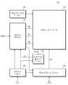
도 1은 본 발명의 제 1 실시 예에 따른 불휘발성 메모리 장치(100)를 보여주는 블록도이다. 도 1을 참조하면, 본 발명의 실시 예에 따른 불휘발성 메모리 장치(100)는 메모리 셀 어레이(110), 어드레스 디코더(120), 기판 모니터 회로(130), 읽기 및 쓰기 회로(140), 제어 로직(150), 그리고 기판 바이어스 회로(160)를 포함한다.1 is a block diagram illustrating a
메모리 셀 어레이(110)는 워드 라인들(WL), 그리고 스트링 선택 라인들(SSL) 및 접지 선택 라인들(GSL)을 포함하는 선택 라인들을 통해 어드레스 디코더(120)에 연결된다. 메모리 셀 어레이(110)는 비트 라인들(BL)을 통해 읽기 및 쓰기 회로(140)에 연결된다. 메모리 셀 어레이(110)는 기판 모니터 회로(130)에 연결된다. 예를 들면, 메모리 셀 어레이(110)의 기판(substrate)이 기판 모니터 회로(130)에 연결될 것이다. 메모리 셀 어레이(110)는 기판 바이어스 회로(160)에 연결된다. 예를 들면, 메모리 셀 어레이(110)의 기판이 기판 바이어스 회로(160)에 연결될 것이다.The
메모리 셀 어레이(110)는 복수의 메모리 블록들을 포함한다. 각 메모리 블록은 복수의 메모리 셀 스트링들을 포함한다. 예를 들면, 각 메모리 블록은 복수의 낸드 스트링들을 포함한다. 각 메모리 셀 스트링은 복수의 메모리 셀들 및 복수의 선택 트랜지스터들을 포함한다. 예를 들면, 각 메모리 셀 스트링은 적어도 하나의 스트링 선택 트랜지스터 및 적어도 하나의 접지 선택 트랜지스터를 포함할 것이다.The
예시적으로, 행 방향으로 배열되는 메모리 셀들은 워드 라인들(WL)에 연결된다. 열 방향으로 배열되는 메모리 셀들은 비트 라인들(BL)에 연결된다. 예를 들면, 열 방향으로 배열되는 메모리 셀들은 복수의 셀 그룹들(예를 들면, 스트링)을 형성할 것이다. 그리고, 복수의 셀 그룹들이 비트 라인들(BL)에 각각 연결될 것이다. 적어도 하나의 스트링 선택 트랜지스터들은 스트링 선택 라인들(SSL)에 연결될 것이다. 적어도 하나의 접지 선택 트랜지스터들은 접지 선택 라인들(GSL)에 연결될 것이다. 예시적으로, 메모리 셀 어레이(110)는 셀 당 하나 또는 그 이상의 비트를 저장할 수 있도록 구성된다.Illustratively, the memory cells arranged in the row direction are connected to the word lines WL. The memory cells arranged in the column direction are connected to the bit lines BL. For example, memory cells arranged in the column direction will form a plurality of cell groups (e.g., strings). Then, a plurality of cell groups will be connected to the bit lines BL, respectively. At least one string select transistor will be connected to the string select lines (SSL). At least one of the ground select transistors will be connected to ground select lines GSL. Illustratively, the
어드레스 디코더(120)는 워드 라인들(WL), 스트링 선택 라인들(SSL), 그리고 접지 선택 라인들(GSL)을 통해 메모리 셀 어레이(110)에 연결된다. 어드레스 디코더(120)는 제어 로직(150)의 제어에 응답하여 동작하도록 구성된다. 어드레스 디코더(120)는 외부로부터 어드레스(ADDR)를 수신한다.The
어드레스 디코더(120)는 수신된 어드레스(ADDR) 중 행 어드레스를 디코딩하도록 구성된다. 디코딩된 행 어드레스를 이용하여, 어드레스 디코더(120)는 메모리 셀 어레이의 메모리 블록을 선택한다. 또한, 디코딩된 행 어드레스를 이용하여, 어드레스 디코더(120)는 선택된 메모리 블록의 워드 라인들(WL), 스트링 선택 라인들(SSL), 그리고 접지 선택 라인(GSL)을 선택한다. 어드레스 디코더(120)는 전달된 어드레스(ADDR) 중 열 어드레스를 추가적으로 디코딩하도록 구성된다. 디코딩된 열 어드레스는 읽기 및 쓰기 회로(140)에 전달된다.The
예시적으로, 어드레스 디코더(120)는 기판 모니터 회로(130)로부터 접지 활성 신호(GE)를 수신하도록 구성된다. 수신된 접지 활성 신호(GE)에 응답하여, 어드레스 디코더(120)는 출력 전압을 조절하도록 구성된다. 예를 들면, 어드레스 디코더(120)는 소거 동작 시에 접지 활성 신호(GE)에 응답하여 동작하도록 구성될 것이다.Illustratively, the
기판 모니터 회로(130)는 메모리 셀 어레이(110) 및 어드레스 디코더(120)에 연결된다. 기판 모니터 회로(130)는 제어 로직(150)의 제어에 응답하여 동작하도록 구성된다. 기판 모니터 회로(130)는 메모리 셀 어레이(110)의 기판 전압(Vsub)을 모니터하도록 구성된다. 메모리 셀 어레이(110)의 기판 전압(Vsub)의 레벨에 응답하여, 기판 모니터 회로(130)는 접지 활성 신호(GE)를 활성화 또는 비활성화 하도록 구성된다. 접지 활성 신호(GE)는 어드레스 디코더(120)에 전달된다. 예를 들면, 기판 모니터 회로(130)는 소거 동작 시에 활성화될 것이다.The
읽기 및 쓰기 회로(140)는 비트 라인들(BL)을 통해 메모리 셀 어레이(110)에 연결된다. 읽기 및 쓰기 회로(140)는 제어 로직(150)의 제어에 응답하여 동작한다. 읽기 및 쓰기 회로(140)는 어드레스 디코더(120)로부터 디코딩된 열 어드레스를 수신하도록 구성된다. 디코딩된 열 어드레스를 이용하여, 읽기 및 쓰기 회로(140)는 비트 라인들(BL)을 선택한다.The read and write
예시적으로, 읽기 및 쓰기 회로(140)는 외부로부터 데이터(DATA)를 수신하고, 수신된 데이터(DATA)를 메모리 셀 어레이(110)에 기입하도록 구성된다. 읽기 및 쓰기 회로(140)는 메모리 셀 어레이(110)로부터 데이터(DATA)를 읽고, 읽어진 데이터(DATA)를 외부로 출력하도록 구성된다. 읽기 및 쓰기 회로(140)는 메모리 셀 어레이(110)의 제 1 저장 영역으로부터 데이터를 읽고, 읽어진 데이터를 메모리 셀 어레이(110)의 제 2 저장 영역에 기입하도록 구성된다. 예를 들면, 읽기 및 쓰기 회로(140)는 카피-백(copy-back) 동작을 수행하도록 구성된다.Illustratively, the read and write
예시적으로, 읽기 및 쓰기 회로(140)는 페이지 버퍼(또는 페이지 레지스터), 열 선택 회로 등과 같이 잘 알려진 구성 요소들을 포함한다. 다른 예로서, 읽기 및 쓰기 회로(140)는 감지 증폭기, 쓰기 드라이버, 열 선택 회로 등과 같이 잘 알려진 구성 요소들을 포함한다.Illustratively, the read and write
제어 로직(150)은 어드레스 디코더(120), 기판 모니터 회로(130), 그리고 읽기 및 쓰기 회로(140) 연결된다. 예를 들면, 제어 로직(150)은 기판 바이어스 회로(160)에 추가적으로 연결될 것이다. 제어 로직(150)은 불휘발성 메모리 장치(100)의 제반 동작을 제어하도록 구성된다. 제어 로직(150)은 외부로부터 전달되는 제어 신호(CTRL)에 응답하여 동작한다.The
기판 바이어스 회로(160)는 제어 로직(150)의 제어에 응답하여 동작한다. 기판 바이어스 회로(160)는 메모리 셀 어레이(110)의 기판을 바이어스하도록 구성된다. 예를 들면, 소거 동작 시에, 기판 바이어스 회로(160)는 메모리 셀 어레이(110)의 기판에 소거 전압(Vers)을 바이어스하도록 구성될 것이다.The
다른 예로서, 기판 모니터 회로(130)는 생략될 수 있다. 이 예에서, 어드레스 디코더(120)는 소거 동작 시에 메모리 셀 어레이(110)의 기판에 전압을 인가하기 전에 특정 지연 시간 동안 대기함으로써 접지 선택 라인(GSL)을 구동할 수 있다. 이 예에서, 지연 시간은 미리 설정될 수 있다. 지연 시간의 길이는 제어 로직(150) 또는 외부 장치에 의해 제공될 수 있다.As another example, the
도 2는 도 1의 메모리 셀 어레이(110)를 보여주는 블록도이다. 도 2를 참조하면, 메모리 셀 어레이(110)는 복수의 메모리 블록들(BLK1~BLKz)을 포함한다. 각 메모리 블록(BLK)은 3차원 구조(또는 수직 구조)를 갖는다. 예를 들면, 각 메모리 블록(BLK)은 제 1 내지 제 3 방향들을 따라 신장된 구조물들을 포함한다. 예를 들면, 각 메모리 블록(BLK)은 제 2 방향을 따라 신장된 복수의 낸드 스트링들(NS)을 포함한다. 예를 들면, 제 1 및 제 3 방향들을 따라 복수의 낸드 스트링들(NS)이 제공될 것이다.2 is a block diagram illustrating the
각 낸드 스트링(NS)은 비트 라인(BL), 적어도 하나의 스트링 선택 라인(SSL), 적어도 하나의 접지 선택 라인(GSL), 워드 라인들(WL), 그리고 공통 소스 라인(CSL)에 연결된다. 즉, 각 메모리 블록은 복수의 비트 라인들(BL), 복수의 스트링 선택 라인들(SSL). 복수의 접지 선택 라인들(GSL), 복수의 워드 라인들(WL), 그리고 복수의 공통 소스 라인(CSL)에 연결될 것이다. 메모리 블록들(BLK1~BLKz)은 도 3을 참조하여 더 상세하게 설명된다.Each NAND string NS is connected to a bit line BL, at least one string select line SSL, at least one ground select line GSL, word lines WL and a common source line CSL . That is, each memory block includes a plurality of bit lines (BL), a plurality of string selection lines (SSL). A plurality of ground select lines GSL, a plurality of word lines WL, and a plurality of common source lines CSL. The memory blocks BLK1 to BLKz are described in more detail with reference to Fig.
메모리 블록들(BLK1~BLKz)은 도 1에 도시된 어드레스 디코더(120)에 의해 선택될 수 있다. 예를 들어, 어드레스 디코더(120)는 메모리 블록들(BLK1~BLKz) 중 디코딩된 행 어드레스에 대응하는 적어도 하나의 메모리 블록을 선택하도록 구성될 수 있다.The memory blocks BLK1 to BLKz may be selected by the
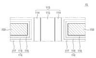
도 3은 도 2의 메모리 블록들(BLK1~BLKz) 중 하나(BLKi)의 제 1 실시 예를 보여주는 사시도이다. 도 4는 도 3의 메모리 블록(BLKi)의 Ⅰ-Ⅰ'선에 따른 단면도이다. 도 3 및 도 4를 참조하면, 메모리 블록(BLKi)은 제 1 내지 제 3 방향들을 따라 신장된 구조물들을 포함한다.3 is a perspective view showing a first embodiment of one of the memory blocks BLK1 to BLKz of FIG. 2 (BLKi). 4 is a cross-sectional view taken along the line I-I 'of the memory block BLKi of FIG. Referring to Figs. 3 and 4, the memory block BLKi includes structures extended along first to third directions.
우선, 기판(111)이 제공된다. 예시적으로, 기판(111)은 제 1 타입을 갖는 웰(well) 일 것이다. 예를 들면, 기판(111)은 붕소(B, Boron)와 같은 3족 원소가 주입되어 형성된 p 웰 일 것이다. 예를 들면, 기판(111)은 n 웰 내에 제공되는 포켓 p 웰 일 것이다. 이하에서, 기판(111)은 p 웰 인 것으로 가정한다. 그러나, 기판(111)은 p 웰 인 것으로 한정되지 않는다.First, a
기판(111) 상에, 제 1 방향을 따라 신장된 복수의 도핑 영역들(311~314)이 제공된다. 예를 들면, 복수의 도핑 영역들(311~314)은 기판(111)과 상이한 제 2 타입을 가질 것이다. 예를 들면, 복수의 도핑 영역들(311~314)은 n 타입을 가질 것이다. 이하에서, 제 1 내지 제 4 도핑 영역들(311~314)은 n 타입을 갖는 것으로 가정한다. 그러나, 제 1 내지 제 4 도핑 영역들(311~314)은 n 타입을 갖는 것으로 한정되지 않는다.On the
제 1 및 제 2 도핑 영역들(311, 312) 사이의 기판(111)의 영역 상에, 제 1 방향을 따라 신장되는 복수의 절연 물질들(112)이 제 2 방향을 따라 순차적으로 제공된다. 예를 들면, 복수의 절연 물질들(112)은 제 2 방향을 따라 특정 거리 만큼 이격되어 제공될 것이다. 예시적으로, 절연 물질들(112)은 실리콘 산화물(Silicon Oxide)과 같은 절연 물질을 포함할 것이다.A plurality of insulating
제 1 및 제 2 도핑 영역들(311, 312) 사이의 기판(111)의 영역 상에, 제 1 방향을 따라 순차적으로 배치되며 제 2 방향을 따라 절연 물질들(112)을 관통하는 복수의 필라들(113)이 제공된다. 예시적으로, 복수의 필라들(113)은 절연 물질들(112)을 관통하여 기판(111)과 연결될 것이다.A plurality of pillars (not shown) disposed sequentially along the first direction on the region of the
예시적으로, 각 필라(113)는 복수의 물질들로 구성될 것이다. 예를 들면, 각 필라(113)의 표면층(114)은 제 1 타입을 갖는 실리콘 물질을 포함할 것이다. 예를 들면, 각 필라(113)의 표면층(114)은 기판(111)과 동일한 타입을 갖는 실리콘 물질을 포함할 것이다. 이하에서, 각 필라(113)의 표면층(114)은 p 타입 실리콘을 포함하는 것으로 가정한다. 그러나, 각 필라(113)의 표면층(114)은 p 타입 실리콘을 포함하는 것으로 한정되지 않는다.Illustratively, each
각 필라(113)의 내부층(115)은 절연 물질로 구성된다. 예를 들면, 각 필라(113)의 내부층(115)은 실리콘 산화물(Silicon Oxide)과 같은 절연 물질을 포함할 것이다. 예를 들면, 각 필라(113)의 내부층(115)은 에어 갭(air gap)을 포함할 수 있다.The
제 1 및 제 2 도핑 영역들(311, 312) 사이의 영역에서, 절연 물질들(112), 필라들(113), 그리고 기판(111)의 노출된 표면을 따라 절연막(116)이 제공된다. 예시적으로, 제 2 방향을 따라 제공되는 마지막 절연 물질(112)의 제 2 방향 쪽의 노출면에 제공되는 절연막(116)은 제거될 수 있다.In an area between the first and second
예시적으로, 절연막(116)의 두께는 절연 물질들(112) 사이의 거리의 1/2 보다 작을 것이다. 즉, 절연 물질들(112) 중 제 1 절연 물질의 하부면에 제공된 절연막(116), 그리고 제 1 절연 물질 하부의 제 2 절연 물질의 상부면에 제공된 절연막(116) 사이에, 절연 물질들(112) 및 절연막(116) 이외의 물질이 배치될 수 있는 영역이 제공될 것이다.Illustratively, the thickness of the insulating
제 1 및 제 2 도핑 영역들(311, 312) 사이의 영역에서, 절연막(116)의 노출된 표면 상에 제 1 도전 물질들(211~291)이 제공된다. 예를 들면, 기판(111)에 인접한 절연 물질(112) 및 기판(111) 사이에 제 1 방향을 따라 신장되는 제 1 도전 물질(211)이 제공된다. 더 상세하게는, 기판(111)에 인접한 절연 물질(112)의 하부면의 절연막(116) 및 기판(111) 사이에, 제 1 방향으로 신장되는 제 1 도전 물질(211)이 제공된다.In the region between the first and second
절연 물질들(112) 중 특정 절연 물질 상부면의 절연막(116) 및 특정 절연 물질 상부에 배치된 절연 물질의 하부면의 절연막(116) 사이에, 제 1 방향을 따라 신장되는 제 1 도전 물질이 제공된다. 예시적으로, 절연 물질들(112) 사이에, 제 1 방향으로 신장되는 복수의 제 1 도전 물질들(221~281)이 제공된다. 예시적으로, 제 1 도전 물질들(211~291)은 금속 물질일 것이다. 예시적으로, 제 1 도전 물질들(211~291)은 폴리 실리콘 등과 같은 도전 물질들일 것이다.A first conductive material extending along the first direction is formed between the insulating
제 2 및 제 3 도핑 영역들(312, 313) 사이의 영역에서, 제 1 및 제 2 도핑 영역들(311, 312) 상의 구조물과 동일한 구조물이 제공될 것이다. 예시적으로, 제 2 및 제 3 도핑 영역들(312, 313) 사이의 영역에서, 제 1 방향으로 신장되는 복수의 절연 물질들(112), 제 1 방향을 따라 순차적으로 배치되며 제 3 방향을 따라 복수의 절연 물질들(112)을 관통하는 복수의 필라들(113), 복수의 절연 물질들(112) 및 복수의 필라들(113)의 노출된 표면에 제공되는 절연막(116), 그리고 제 1 방향을 따라 신장되는 복수의 제 1 도전 물질들(212~292)이 제공된다.In the region between the second and third
제 3 및 제 4 도핑 영역들(313, 314) 사이의 영역에서, 제 1 및 제 2 도핑 영역들(311, 312) 상의 구조물과 동일한 구조물이 제공될 것이다. 예시적으로, 제 3 및 제 4 도핑 영역들(312, 313) 사이의 영역에서, 제 1 방향으로 신장되는 복수의 절연 물질들(112), 제 1 방향을 따라 순차적으로 배치되며 제 3 방향을 따라 복수의 절연 물질들(112)을 관통하는 복수의 필라들(113), 복수의 절연 물질들(112) 및 복수의 필라들(113)의 노출된 표면에 제공되는 절연막(116), 그리고 제 1 방향을 따라 신장되는 복수의 제 1 도전 물질들(213~293)이 제공된다.In the region between the third and fourth
복수의 필라들(113) 상에 드레인들(320)이 각각 제공된다. 예시적으로, 드레인들(320)은 제 2 타입으로 도핑된 실리콘 물질들일 것이다. 예를 들면, 드레인들(320)은 n 타입으로 도핑된 실리콘 물질들일 것이다. 이하에서, 드레인들(320)는 n 타입 실리콘을 포함하는 것으로 가정한다. 그러나, 드레인들(320)은 n 타입 실리콘을 포함하는 것으로 한정되지 않는다. 예시적으로, 각 드레인(320)의 폭은 대응하는 필라(113)의 폭 보다 클 수 있다. 예를 들면, 각 드레인(320)은 대응하는 필라(113)의 상부면에 패드 형태로 제공될 수 있다.
드레인들(320) 상에, 제 3 방향으로 신장된 제 2 도전 물질들(331~333)이 제공된다. 제 2 도전 물질들(331~333)은 제 1 방향을 따라 순차적으로 배치된다. 제 2 도전 물질들(331~333) 각각은 대응하는 영역의 드레인들(320)과 연결된다. 예시적으로, 드레인들(320) 및 제 3 방향으로 신장된 제 2 도전 물질(333)은 각각 콘택 플러그들(contact plug)을 통해 연결될 수 있다. 예시적으로, 제 2 도전 물질들(331~333)은 금속 물질들일 것이다. 예시적으로, 제 2 도전 물질들(331~333)은 폴리 실리콘 등과 같은 도전 물질들일 것이다.On the
이하에서, 제 1 도전 물질들(211~291, 212~292, 213~293)의 높이가 정의된다. 제 1 도전 물질들(211~291, 212~292, 213~293)은 기판(111)으로부터 순차적으로 제 1 내지 제 9 높이를 갖는 것으로 정의된다. 즉, 기판(111)과 인접한 제 1 도전 물질들(211~213)은 제 1 높이를 갖는다. 제 2 도전 물질들(331~333)과 인접한 제 1 도전 물질들(291~293)은 제 9 높이를 갖는다. 제 1 도전 물질 및 기판(111) 사이의 거리가 증가할수록, 제 1 도전 물질의 높이는 증가한다.Hereinafter, the heights of the first
도 3 및 도 4에서, 각 필라(113)는 절연막(116)의 인접한 영역 및 복수의 제 1 도전 물질들(211~291, 212~292, 213~293) 중 인접한 영역과 함께 스트링을 형성한다. 예를 들면, 각 필라(113)는 절연막(116)의 인접한 영역 및 제 1 도전 물질들(211~291, 212~292, 213~293) 중 인접한 영역과 함께 낸드 스트링(NS)을 형성한다. 낸드 스트링(NS)은 복수의 트랜지스터 구조들(TS)을 포함한다. 트랜지스터 구조(TS)는 도 5를 참조하여 더 상세하게 설명된다. 예시적으로, 특정 스트링의 복수의 트랜지스터 구조들(TS)의 부분집합은 서브스트링일 수 있다.3 and 4, each
도 5는 도 4의 트랜지스터 구조(TS)를 보여주는 단면도이다. 도 3 내지 도 5를 참조하면, 절연막(116)은 제 1 내지 제 3 서브 절연막들(117, 118, 119)을 포함한다.5 is a cross-sectional view showing the transistor structure (TS) of Fig. Referring to FIGS. 3 to 5, the insulating
필라(113)의 p 타입 실리콘을 포함하는 표면층(114)은 바디(body)로 동작할 것이다. 필라(113)에 인접한 제 1 서브 절연막(117)은 터널링 절연막으로 동작할 것이다. 예를 들면, 필라(113)에 인접한 제 1 서브 절연막(117)은 열산화막을 포함할 것이다.The
제 2 서브 절연막(118)은 전하 저장막으로 동작할 것이다. 예를 들면, 제 2 서브 절연막(118)은 전하 포획층으로 동작할 것이다. 예를 들면, 제 2 서브 절연막(118)은 질화막 또는 금속 산화막(예를 들면, 알루미늄 산화막, 하프늄 산화막 등)을 포함할 것이다.The second
제 1 도전 물질(233)에 인접한 제 3 서브 절연막(119)은 블로킹 절연막으로 동작할 것이다. 예시적으로, 제 1 방향으로 신장된 제 1 도전 물질(233)과 인접한 제 3 서브 절연막(119)은 단일층 또는 다층으로 형성될 수 있다. 제 3 서브 절연막(119)은 제 1 및 제 2 서브 절연막들(117, 118) 보다 높은 유전상수를 갖는 고유전막(예를 들면, 알루미늄 산화막, 하프늄 산화막 등)일 수 있다.The third
제 1 도전 물질(233)은 게이트(또는 제어 게이트)로 동작할 것이다. 즉, 게이트(또는 제어 게이트)로 동작하는 제 1 도전 물질(233), 블로킹 절연막으로 동작하는 제 3 서브 절연막(119), 전하 저장막으로 동작하는 제 2 서브 절연막(118), 터널링 절연막으로 동작하는 제 1 서브 절연막(117), 그리고 바디로 동작하는 p 타입 실리콘을 포함하는 표면층(114)은 트랜지스터(또는 메모리 셀 트랜지스터 구조)를 형성할 것이다. 예시적으로, 제 1 내지 제 3 서브 절연막들(117~119)은 ONO (oxide-nitride-oxide)를 구성할 수 있다. 이하에서, 필라(113)의 p 타입 실리콘을 포함하는 표면층(114)을 제 2 방향의 바디라 부르기로 한다. 예시적으로, 필라(113), 절연막(116), 그리고 제 1 도전 물질(233) 사이의 각도는 직각, 예각, 또는 둔각일 수 있다.The first
메모리 블록(BLKi)에서, 사나의 필라(113)는 하나의 낸드 스트링(NS)에 대응한다. 메모리 블록(BLKi)은 복수의 필라들(113)을 포함한다. 즉, 메모리 블록(BLKi)은 복수의 낸드 스트링들(NS)을 포함한다. 더 상세하게는, 메모리 블록(BLKi)은 제 2 방향(또는 기판과 수직한 방향)으로 신장된 복수의 낸드 스트링들(NS)을 포함한다.In memory block BLKi, Sana's
각 낸드 스트링(NS)은 제 2 방향을 따라 배치되는 복수의 트랜지스터 구조들(TS)을 포함한다. 각 낸드 스트링(NS)의 복수의 트랜지스터 구조들(TS) 중 적어도 하나는 스트링 선택 트랜지스터(SST)로 동작한다. 각 낸드 스트링(NS)의 복수의 트랜지스터 구조들(TS) 중 적어도 하나는 접지 선택 트랜지스터(GST)로 동작한다.Each NAND string NS includes a plurality of transistor structures TS disposed along a second direction. At least one of the plurality of transistor structures TS of each NAND string NS operates as a string selection transistor (SST). At least one of the plurality of transistor structures TS of each NAND string NS operates as a ground selection transistor GST.
게이트들(또는 제어 게이트들)은 제 1 방향으로 신장된 제 1 도전 물질들(211~291, 212~292, 213~293)에 대응한다. 즉, 게이트들(또는 제어 게이트들)은 제 1 방향으로 신장되어 워드 라인들, 그리고 적어도 두 개의 선택 라인들(예를 들면, 적어도 하나의 스트링 선택 라인(SSL) 및 적어도 하나의 접지 선택 라인(GSL))을 형성한다.The gates (or control gates) correspond to the first conductive materials 211-291, 212-292, 213-293 extended in the first direction. That is, the gates (or control gates) extend in a first direction to form word lines and at least two select lines (e.g., at least one string select line SSL and at least one ground select line GSL).
제 3 방향으로 신장된 제 2 도전 물질들(331~333)은 낸드 스트링들(NS)의 일단에 연결된다. 예시적으로, 제 3 방향으로 신장된 제 2 도전 물질들(331~333)은 비트 라인들(BL)로 동작한다. 즉, 하나의 메모리 블록(BLKi)에서, 하나의 비트 라인(BL)에 복수의 낸드 스트링들이 연결된다.The second
제 1 방향으로 신장된 제 2 타입 도핑 영역들(311~314)이 낸드 스트링들의 타단에 제공된다. 제 1 방향으로 신장된 제 2 타입 도핑 영역들(311~314)은 공통 소스 라인(CSL)으로 동작한다.Second type doped regions 311-314 extending in a first direction are provided at the other end of the NAND strings. The second type doped regions 311-314 extending in the first direction act as a common source line (CSL).
요약하면, 메모리 블록(BLKi)은 기판(111)에 수직한 방향(제 2 방향)으로 신장된 복수의 낸드 스트링들을 포함하며, 하나의 비트 라인(BL)에 복수의 낸드 스트링들(NS)이 연결되는 낸드 플래시 메모리 블록(예를 들면, 전하 포획형)으로 동작한다.In summary, the memory block BLKi includes a plurality of NAND strings extended in a direction perpendicular to the substrate 111 (second direction), and a plurality of NAND strings NS are formed on one bit line BL And operates as a connected NAND flash memory block (for example, charge capturing type).
도 3 내지 도 5에서, 제 1 방향으로 신장되는 도체 라인들(211~291, 212~292, 213~293)은 9 개의 층에 제공되는 것으로 설명되었다. 그러나, 제 1 방향으로 신장되는 도체 라인들(211~291, 212~292, 213~293)은 9 개의 층에 제공되는 것으로 한정되지 않는다. 예를 들면, 제 1 방향으로 신장되는 도체 라인들은 8개의 층, 16개의 층, 또는 복수의 층에 제공될 수 있다. 즉, 하나의 낸드 스트링에서, 트랜지스터는 8개, 16개, 또는 복수개일 수 있다. 또한, 제 1 도전 물질들은 메모리 셀들을 구성하는 복수의 층들, 그리고 선택 트랜지스터들을 구성하는 적어도 두 개의 층들에 제공될 수 있다. 예를 들어, 제 1 도전 물질들은 더미 메모리 셀들을 구성하는 층에 제공될 수 있다.3 to 5, it has been described that the
도 3 내지 도 5에서, 하나의 비트 라인(BL)에 3 개의 낸드 스트링들(NS)이 연결되는 것으로 설명되었다. 그러나, 하나의 비트 라인(BL)에 3개의 낸드 스트링들(NS)이 연결되는 것으로 한정되지 않는다. 예시적으로, 메모리 블록(BLKi)에서, 하나의 비트 라인(BL)에 m 개의 낸드 스트링들(NS)이 연결될 수 있다. 이때, 하나의 비트 라인(BL)에 연결되는 낸드 스트링들(NS)의 수 만큼, 제 1 방향으로 신장되는 제 1 도전 물질들(211~291, 212~292, 213~293)의 수 및 공통 소스 라인(CSL)으로 동작하는 도핑 영역들(311~314)의 수 또한 조절될 것이다.3 to 5, it has been described that three NAND strings NS are connected to one bit line BL. However, it is not limited that three NAND strings NS are connected to one bit line BL. Illustratively, in the memory block BLKi, m NAND strings NS may be connected to one bit line BL. At this time, the number of the first
도 3 내지 도 5에서, 제 1 방향으로 신장된 하나의 제 1 도전 물질에 3 개의 낸드 스트링들(NS)이 연결되는 것으로 설명되었다. 그러나, 하나의 제 1 도전 물질에 3 개의 낸드 스트링들(NS)이 연결되는 것으로 한정되지 않는다. 예를 들면, 하나의 제 1 도전 물질에, n 개의 낸드 스트링들(NS)이 연결될 수 있다. 이때, 하나의 제 1 도전 물질에 연결되는 낸드 스트링들(NS)의 수 만큼, 비트 라인들(331~333)의 수 또한 조절될 것이다.3 to 5, it has been described that three NAND strings NS are connected to one first conductive material extending in a first direction. However, it is not limited that three NAND strings NS are connected to one first conductive material. For example, to one first conductive material, n NAND strings NS may be connected. At this time, the number of
예시적으로, 필라(113)의 제 1 및 제 3 방향에 따른 단면적은 기판(111)과 가까울수록 감소할 수 있다. 예를 들면, 공정 상의 특성 또는 오차에 의해, 필라(113)의 제 1 및 제 3 방향에 따른 단면적이 가변될 수 있다.Illustratively, the cross sectional area along the first and third directions of the
예시적으로, 필라(113)는 식각에 의해 형성된 홀에 실리콘 물질 및 절연 물질과 같은 물질들이 제공되어 형성된다. 식각되는 깊이가 증가할수록, 식각에 의해 형성되는 홀의 제 1 및 제 3 방향에 따른 면적은 감소할 수 있다. 즉, 필라(113)의 제 1 및 제 3 방향에 따른 단면적은 기판(111)에 가까울수록 감소할 수 있다.Illustratively, the
도 6은 도 3 내지 도 5를 참조하여 설명된 메모리 블록(BLKi)의 등가 회로를 보여주는 회로도이다. 도 3 내지 도 6을 참조하면, 제 1 비트 라인(BL1) 및 공통 소스 라인(CSL) 사이에 낸드 스트링들(NS11~NS31)이 제공된다. 제 2 비트 라인(BL2) 및 공통 소스 라인(CSL) 사이에 낸드 스트링들(NS12, NS22, NS32)이 제공된다. 제 3 비트 라인(BL3) 및 공통 소스 라인(CSL) 사이에, 낸드 스트링들(NS13, NS23. NS33)이 제공된다. 제 1 내지 제 3 비트 라인들(BL1~BL3)은 제 3 방향으로 신장된 제 2 도전 물질들(331~333)에 각각 대응할 것이다.Fig. 6 is a circuit diagram showing an equivalent circuit of the memory block BLKi described with reference to Figs. 3 to 5. Fig. Referring to Figs. 3-6, NAND strings NS11-NS31 are provided between the first bit line BL1 and the common source line CSL. NAND strings NS12, NS22, and NS32 are provided between the second bit line BL2 and the common source line CSL. Between the third bit line BL3 and the common source line CSL, NAND strings NS13, NS23, NS33 are provided. The first to third bit lines BL1 to BL3 correspond to the second
각 낸드 스트링(NS)의 스트링 선택 트랜지스터(SST)는 대응하는 비트 라인(BL)과 연결된다. 각 낸드 스트링(NS)의 접지 선택 트랜지스터(GST)는 공통 소스 라인(CSL)과 연결된다. 각 낸드 스트링(NS)의 스트링 선택 트랜지스터(SST) 및 접지 선택 트랜지스터(GST) 사이에 메모리 셀들(MC)이 제공된다.The string selection transistor SST of each NAND string NS is connected to the corresponding bit line BL. The ground selection transistor GST of each NAND string NS is connected to the common source line CSL. Memory cells MC are provided between the string selection transistor SST and the ground selection transistor GST of each NAND string NS.
이하에서, 행 및 열 단위로 낸드 스트링들(NS)을 정의한다. 하나의 비트 라인에 공통으로 연결된 낸드 스트링들(NS)은 하나의 열을 형성한다. 예를 들면, 제 1 비트 라인(BL1)에 연결된 낸드 스트링들(NS11~NS31)은 제 1 열에 대응할 것이다. 제 2 비트 라인(BL2)에 연결된 낸드 스트링들(NS12~NS32)은 제 2 열에 대응할 것이다. 제 3 비트 라인(BL3)에 연결된 낸드 스트링들(NS13~NS33)은 제 3 열에 대응할 것이다.In the following, NAND strings NS are defined in units of rows and columns. The NAND strings NS connected in common to one bit line form one column. For example, the NAND strings NS11 to NS31 connected to the first bit line BL1 will correspond to the first column. NAND strings NS12 to NS32 connected to the second bit line BL2 will correspond to the second column. The NAND strings NS13 to NS33 connected to the third bit line BL3 will correspond to the third column.
하나의 스트링 선택 라인(SSL)에 연결되는 낸드 스트링들(NS)은 하나의 행을 형성한다. 예를 들면, 제 1 스트링 선택 라인(SSL1)에 연결된 낸드 스트링들(NS11~NS13)은 제 1 행을 형성한다. 제 2 스트링 선택 라인(SSL2)에 연결된 낸드 스트링들(NS21~NS23)은 제 2 행을 형성한다. 제 3 스트링 선택 라인(SSL3)에 연결된 낸드 스트링들(NS31~NS33)은 제 3 행을 형성한다.NAND strings NS connected to one string select line SSL form one row. For example, the NAND strings NS11 to NS13 connected to the first string selection line SSL1 form a first row. The NAND strings NS21 to NS23 connected to the second string selection line SSL2 form a second row. The NAND strings NS31 to NS33 connected to the third string selection line SSL3 form the third row.
각 낸드 스트링(NS)에서, 높이가 정의된다. 예시적으로, 각 낸드 스트링(NS)에서, 접지 선택 트랜지스터(GST)의 높이는 1인 것으로 정의된다. 접지 선택 트랜지스터(GST)에 인접한 메모리 셀(MC1)의 높이는 2인 것으로 정의된다. 스트링 선택 트랜지스터(SST)의 높이는 9로 정의된다. 스트링 선택 트랜지스터(SST)와 인접한 메모리 셀(MC7)의 높이는 8로 정의된다. 메모리 셀(MC) 및 접지 선택 트랜지스터(GST) 사이의 거리가 증가할수록, 메모리 셀(MC)의 높이는 증가한다. 즉, 제 1 내지 제 7 메모리 셀들(MC1~MC7)은 각각 제 2 내지 제 8 높이를 갖는 것으로 정의된다.For each NAND string NS, the height is defined. Illustratively, in each NAND string NS, the height of the ground selection transistor GST is defined as one. The height of the memory cell MC1 adjacent to the ground selection transistor GST is defined as two. The height of the string selection transistor (SST) is defined as 9. The height of the memory cell MC7 adjacent to the string selection transistor SST is defined as eight. As the distance between the memory cell MC and the ground selection transistor GST increases, the height of the memory cell MC increases. That is, the first to seventh memory cells MC1 to MC7 are defined to have the second to eighth heights, respectively.
동일한 행의 낸드 스트링들(NS)은 접지 선택 라인(GSL)을 공유한다. 상이한 행의 낸드 스트링들(NS)은 접지 선택 라인들(GSL)을 공유한다. 제 1 높이를 갖는 제 1 도전 물질들(211~213)이 서로 연결되어 접지 선택 라인(GSL)을 형성할 것이다.NAND strings NS in the same row share the ground selection line GSL. The NAND strings NS in the different rows share the ground selection lines GSL. The first
동일한 행의 낸드 스트링들(NS)의 동일한 높이의 메모리 셀들(MC)은 워드 라인(WL)을 공유한다. 동일한 높이를 가지며 상이한 행에 대응하는 낸드 스트링들(NS)의 워드 라인들(WL)은 공통으로 연결된다. 즉, 동일한 높이의 메모리 셀들(MC)은 워드 라인(WL)을 공유한다.The memory cells MC at the same height of the NAND strings NS in the same row share the word line WL. The word lines WL of the NAND strings NS having the same height and corresponding to the different rows are connected in common. That is, the memory cells MC of the same height share the word line WL.
제 2 높이를 갖는 제 1 도전 물질들(221~223)이 공통으로 연결되어 제 1 워드 라인(WL1)을 형성한다. 제 3 높이를 갖는 제 1 도전 물질들(231~233)이 공통으로 연결되어 제 2 워드 라인(WL2)을 형성한다. 제 4 높이를 갖는 제 1 도전 물질들(241~243)이 공통으로 연결되어 제 3 워드 라인(WL3)을 형성한다. 제 5 높이를 갖는 제 1 도전 물질들(251~253)이 공통으로 연결되어 제 4 워드 라인(WL4)을 형성한다. 제 6 높이를 갖는 제 1 도전 물질들(261~263)이 공통으로 연결되어 제 5 워드 라인(WL5)을 형성한다. 제 7 높이를 갖는 제 1 도전 물질들(271~273)이 공통으로 연결되어 제 6 워드 라인(WL6)을 형성한다. 제 8 높이를 갖는 제 1 도전 물질들(281~283)이 공통으로 연결되어 제 7 워드 라인(WL7)을 형성한다.The first
동일한 행의 낸드 스트링들(NS)은 스트링 선택 라인(SSL)을 공유한다. 상이한 행의 낸드 스트링들(NS)은 상이한 스트링 선택 라인들(SSL1, SSL2, SSL3)에 각각 연결된다. 제 1 내지 제 3 스트링 선택 라인들(SSL1~SSL3)은 각각 제 9 높이를 갖는 제 1 도전 물질들(291~293)에 대응할 것이다.The NAND strings NS in the same row share a string selection line (SSL). The NAND strings NS in the different rows are connected to the different string selection lines SSL1, SSL2 and SSL3, respectively. The first through third string selection lines SSL1 through SSL3 may correspond to the first
이하에서, 제 1 스트링 선택 트랜지스터들(SST1)은 제 1 스트링 선택 라인(SSL1)에 연결된 스트링 선택 트랜지스터들(SST)로 정의된다. 제 2 스트링 선택 트랜지스터들(SST2)은 제 2 스트링 선택 라인(SSL2)에 연결된 스트링 선택 트랜지스터들(SST)로 정의된다. 제 3 스트링 선택 트랜지스터들(SST3)은 제 3 스트링 선택 라인(SSL3)에 연결된 스트링 선택 트랜지스터들(SST)로 정의된다.Hereinafter, the first string selection transistors SST1 are defined as string selection transistors SST connected to the first string selection line SSL1. The second string selection transistors SST2 are defined as string selection transistors SST connected to the second string selection line SSL2. The third string selection transistors SST3 are defined as string selection transistors SST connected to the third string selection line SSL3.
공통 소스 라인(CSL)은 낸드 스트링들(NS)에 공통으로 연결된다. 예를 들면, 기판(111) 상의 활성 영역에서, 제 1 내지 제 4 도핑 영역들(311~314)이 서로 연결되어 공통 소스 라인(CSL)을 형성할 것이다.The common source line CSL is connected in common to the NAND strings NS. For example, in the active region on the
도 6에 도시된 바와 같이, 동일 높이의 워드 라인들(WL)은 공통으로 연결되어 있다. 따라서, 특정 높이의 워드 라인(WL)이 선택될 때, 선택된 워드 라인(WL)에 연결된 모든 낸드 스트링들(NS)이 선택될 것이다. 상이한 행의 낸드 스트링들(NS)은 상이한 스트링 선택 라인(SSL)에 연결되어 있다. 따라서, 스트링 선택 라인들(SSL1~SSL3)을 선택 및 비선택함으로써, 동일 워드 라인(WL)에 연결된 낸드 스트링들(NS) 중 비선택 행의 낸드 스트링들(NS)이 대응하는 비트 라인으로부터 분리되고 그리고 선택 행의 낸드 스트링들(NS)이 대응하는 비트 라인에 연결될 수 있다.As shown in FIG. 6, the word lines WL of the same height are connected in common. Thus, when the word line WL of a particular height is selected, all of the NAND strings NS connected to the selected word line WL will be selected. NAND strings NS in different rows are connected to different string select lines SSL. Thus, by selecting and deselecting the string selection lines SSL1 to SSL3, the NAND strings NS of unselected rows among the NAND strings NS connected to the same word line WL are separated from the corresponding bit lines And the NAND strings NS of the selected row may be connected to the corresponding bit line.
즉, 스트링 선택 라인들(SSL1~SSL3)을 선택 및 비선택함으로써, 낸드 스트링들(NS)의 행이 선택될 수 있다. 그리고, 비트 라인들(BL1~BL3)을 선택함으로써, 선택 행의 낸드 스트링들(NS)이 열 단위로 선택될 수 있다.That is, by selecting and deselecting the string selection lines SSL1 to SSL3, a row of NAND strings NS can be selected. Then, by selecting the bit lines BL1 to BL3, the NAND strings NS of the selected row can be selected in units of columns.
예시적으로, 프로그램 및 읽기 동작 시에, 선택 행의 선택 워드 라인에 선택 전압이 인가되고, 비선택 워드 라인들에 비선택 전압이 인가될 것이다. 예를 들면, 선택 전압은 프로그램 전압(Vpgm) 또는 읽기 전압(Vr)일 것이다. 예를 들면, 비선택 전압은 패스 전압(Vpass) 또는 비선택 읽기 전압(Vread)일 것이다. 즉,프로그램 및 읽기 동작은 낸드 스트링들(NS11~NS13, NS21~NS23, NS31~NS33)의 선택 행의 워드 라인 단위로 수행될 것이다.Illustratively, during a program and read operation, a select voltage is applied to the selected word line of the selected row and a non-selected voltage is applied to the unselected word lines. For example, the select voltage may be the program voltage Vpgm or the read voltage Vr. For example, the unselected voltage may be a pass voltage (Vpass) or an unselected read voltage (Vread). That is, the program and read operations will be performed in word line units of the selected row of NAND strings (NS11 to NS13, NS21 to NS23, NS31 to NS33).
예시적으로, 제 1 도전 물질들(211~291, 212~292), 213~293) 중 선택 라인들로 동작하는 제 1 도전 물질들과 워드 라인들로 동작하는 제 1 도전 물질들 사이의 절연 물질들(112)의 두께는 다른 절연 물질들(112)의 두께보다 두꺼울 수 있다.Illustratively, isolation between the first conductive materials operating with the select lines of the first conductive materials 211-291, 212-292, 213-293 and the first conductive materials operating with the word lines, The thickness of the
도 3 내지 도 6에서, 제 1 높이를 갖는 제 1 도전 물질들(211, 212, 213)은 접지 선택 라인(GSL)으로 동작하고, 제 9 높이를 갖는 제 1 도전 물질들(291, 292, 293)은 스트링 선택 라인들(SSL1, SSL2, SSL3)로 동작한다.3 to 6, the first
이때, 제 1 높이를 갖는 제 1 도전 물질들(211, 212, 213)과 제 2 높이를 갖는 제 1 도전 물질들(221, 222, 223) 사이의 절연 물질들(112)의 두께는 제 2 높이를 갖는 제 1 도전 물질들(221, 222, 223)과 제 8 높이를 갖는 제 1 도전 물질들(281, 282, 283) 사이의 절연 물질들(112)보다 두꺼울 수 있다.At this time, the thickness of the insulating
마찬가지로, 제 8 높이를 갖는 제 1 도전 물질들(281, 282, 283)과 제 9 높이를 갖는 제 1 도전 물질들(291, 292, 293) 사이의 절연 물질(112)의 두께는 제 2 높이를 갖는 제 1 도전 물질들(221, 222, 223)과 제 8 높이를 갖는 제 1 도전 물질들(281, 282, 283) 사이의 절연 물질들(112)보다 두꺼울 수 있다.Likewise, the thickness of the insulating
이하에서, 프로그램될 메모리 셀에 대응하는 비트 라인을 선택 비트 라인이라 부르기로 한다. 그리고, 프로그램 금지될 메모리 셀에 대응하는 비트 라인을 비선택 비트 라인이라 부르기로 한다.Hereinafter, a bit line corresponding to a memory cell to be programmed will be referred to as a selected bit line. The bit line corresponding to the memory cell to be program inhibited will be referred to as a non-selected bit line.
이하에서, 프로그램 동작 시에, 낸드 스트링들(NS11~NS13, NS21~NS23, NS31~NS33)의 제 1 행이 선택되는 것으로 가정한다. 그리고, 제 2 비트 라인(BL2)이 선택되는 것으로 가정한다. 또한, 제 1 및 제 3 비트 라인들(BL1, BL3)이 비선택되는 것으로 가정한다.Hereinafter, it is assumed that the first row of the NAND strings NS11 to NS13, NS21 to NS23, and NS31 to NS33 is selected during the program operation. It is assumed that the second bit line BL2 is selected. It is also assumed that the first and third bit lines BL1 and BL3 are unselected.
도 7은 도 1의 불휘발성 메모리 장치의 소거 동작 시의 전압 조건의 실시 예를 보여주는 테이블이다. 예시적으로, 소거 동작은 메모리 블록 단위로 수행될 것이다. 예시적으로, 도 3 내지 도 6을 참조하여 설명된 메모리 블록(BLKi)을 참조하여, 소거 동작이 설명된다.7 is a table showing an embodiment of a voltage condition in the erase operation of the nonvolatile memory device of FIG. Illustratively, the erase operation will be performed on a memory block basis. Illustratively, with reference to the memory block BLKi described with reference to Figs. 3 to 6, the erase operation is described.
소거 동작 시에, 스트링 선택 라인들(SSL1~SSL3)은 플로팅된다. 워드 라인들(WL1~WL7)에 워드 라인 소거 전압(Vwe)이 인가된다. 예를 들면, 워드 라인 소거 전압(Vwe)은 접지 전압(Vss)일 것이다. 접지 선택 라인(GSL)은 플로팅된다. 그리고, 기판(111)에 소거 전압(Vers)이 인가된다.In the erase operation, the string selection lines SSL1 to SSL3 are floated. The word line erase voltage Vwe is applied to the word lines WL1 to WL7. For example, the word line erase voltage Vwe may be the ground voltage Vss. The ground select line GSL is floated. Then, the erase voltage Vers is applied to the
기판(111) 및 제 2 방향의 바디(114)는 동일한 타입의 실리콘 물질로 구성된다. 따라서, 기판(111)에 인가되는 소거 전압(Vers)은 제 2 방향의 바디(114)로 전달된다. 예시적으로, 소거 전압(Vers)은 고전압일 것이다.The
접지 선택 라인(GSL) 및 스트링 선택 라인들(SSL1~SSL3)은 플로팅 상태이다. 따라서, 제 2 방향의 바디(114)의 전압이 변화할 때, 접지 선택 라인(GSL) 및 스트링 선택 라인들(SSL1~SSL3)은 커플링의 영향을 받는다. 즉, 제 2 방향의 바디(114)의 전압이 소거 전압(Vers)으로 상승할 때, 접지 선택 라인(GSL) 및 스트링 선택 라인들(SSL1~SSL3)의 전압 또한 상승할 것이다. 따라서, 접지 선택 트랜지스터들(GST) 및 스트링 선택 트랜지스터들(GST)은 소거 방지된다.The ground selection line GSL and the string selection lines SSL1 to SSL3 are in a floating state. Therefore, when the voltage of the
워드 라인들(WL1~WL7)에 워드 라인 소거 전압(Vwe)이 인가된다. 예시적으로, 워드 라인 소거 전압(Vwe)은 저전압이다. 예를 들면, 워드 라인 소거 전압(Vwe)은 접지 전압(Vss)일 것이다. 제 2 방향의 바디(114) 및 워드 라인들(WL1~WL7) 사이의 전압 차이에 의해, 메모리 셀들(MC1~MC7)에서 Fowler-Nordheim 터널링이 발생할 것이다. 따라서, 메모리 셀들(MC1~MC7)은 소거될 것이다.The word line erase voltage Vwe is applied to the word lines WL1 to WL7. Illustratively, the word line erase voltage Vwe is a low voltage. For example, the word line erase voltage Vwe may be the ground voltage Vss. Due to the voltage difference between the
기판(111)에 소거 전압(Vers)이 인가될 때, 기판(111) 및 접지 선택 라인(GSL) 사이에 커플링이 발생할 수 있다. 예를 들면, 기판(111)의 전압이 상승할 때, 커플링의 영향에 의해 접지 선택 라인(GSL)의 전압 또한 상승할 수 있다. 접지 선택 라인(GSL)의 전압이 상승하면, 접지 선택 트랜지스터들(GST)이 턴-온 될 수 있다. 즉, 제 2 방향의 바디(114) 중 접지 선택 트랜지스터들(GST)에 대응하는 영역이 반전될 수 있다.When the erase voltage Vers is applied to the
도 8은 도 3 내지 도 6을 참조하여 설명된 메모리 블록(BLKi)의 낸드 스트링들(NS11~NS13, NS21~NS23, NS31~NS33) 중 하나(NS12)를 보여주는 단면도이다. 예시적으로, 소거 동작 시에 접지 선택 트랜지트러(GST)가 턴-온 된 경우가 도 8에 도시되어 있다.8 is a cross-sectional view showing one of the NAND strings NS11 to NS13, NS21 to NS23, and NS31 to NS33 of the memory block BLKi described with reference to FIGS. 3 to 6 (NS12). Illustratively, the case in which the ground selection transistor GST is turned on during the erase operation is shown in FIG.
도 3 내지 도 8을 참조하면, 기판(111)은 p-타입 실리콘이다. 제 2 방향의 바디(114) 중 스트링 선택 트랜지스터(SST) 및 메모리 셀들(MC1~MC7)에 대응하는 영역은 p-타입을 유지한다. 반면, 제 2 방향의 바디(114) 중 접지 선택 트랜지스터(GST)에 대응하는 영역(N1)은 n-타입으로 반전되어 있다. 즉, 제 2 방향의 바디(114) 중 스트링 선택 트랜지스터(SST) 및 메모리 셀들(MC1~MC7)에 대응하는 영역과 기판(111)은 전기적으로 절연된다. 따라서, 기판(111)에 인가되는 소거 전압(Vers)이 제 2 방향의 바디(114) 중 메모리 셀들(MC1~MC7)에 전달되지 않으며, 메모리 셀들(MC1~MC7)은 소거되지 않는다. 즉, 소거 교란이 발생한다.3-8, the
이와 같은 문제를 방지하기 위하여, 본 발명의 실시 예에 따른 불휘발성 메모리 장치는 메모리 셀 어레이(110)의 기판의 전압 레벨에 따라 접지 선택 라인을 구동하도록 구성된다.In order to prevent such a problem, the nonvolatile memory device according to the embodiment of the present invention is configured to drive the ground selection line according to the voltage level of the substrate of the
도 9는 도 1의 불휘발성 메모리 장치(100)의 소거 방법을 보여주는 순서도이다. 예시적으로, 메모리 셀 어레이(110)의 메모리 블록들(BLK1~BLKz) 중 도 3 내지 도 6을 참조하여 설명된 메모리 블록(BLKi)이 소거되는 것으로 가정한다. 즉, 어드레스 디코더(120)의 블록 선택 회로(121)은 메모리 블록(BLKi)을 선택하는 것으로 가정한다.FIG. 9 is a flowchart showing an erasing method of the
도 1 내지 도 6, 그리고 도 9를 참조하면, S110 단계에서, 워드 라인들(WL1~WL7)에 워드 라인 소거 전압(Vwe)이 인가된다. 예를 들면, 워드 라인 소거 전압(Vwe)은 저전압이다. 예를 들면, 워드 라인 소거 전압(Vwe)은 접지 전압(Vss)이다. 예를 들면, 워드 라인 소거 전압(Vwe)은 접지 전압(Vss) 보다 낮은 레벨을 갖는다. 예를 들면, 어드레스 디코더(120)는 워드 라인들(WL1~WL7)을 워드 라인 소거 전압(Vwe)으로 구동할 것이다.Referring to FIGS. 1 to 6 and 9, in step S110, a word line erase voltage Vwe is applied to the word lines WL1 to WL7. For example, the word line erase voltage Vwe is a low voltage. For example, the word line erase voltage Vwe is the ground voltage Vss. For example, the word line erase voltage Vwe has a level lower than the ground voltage Vss. For example, the
S120 단계에서, 접지 선택 라인(GSL)에 미리 설정된 전압(Vpd)이 인가된다. 예를 들면, 미리 설정된 전압(Vpd)은 접지 선택 트랜지스터(GST)를 턴-오프 하는 전압이다. 예를 들면, 미리 설정된 전압(Vpd)은 접지 선택 트랜지스터(GST)의 문턱 전압보다 낮은 레벨을 갖는다. 예를 들면, 미리 설정된 전압(Vpd)은 접지 전압(Vss)이다. 예를 들면, 미리 설정된 전압(Vpd)은 접지 전압(Vss) 보다 낮은 레벨을 갖는다. 예를 들면, 어드레스 디코더(120)는 접지 선택 라인(GSL)을 미리 설정된 전압(Vpd)으로 구동할 것이다.In step S120, a preset voltage Vpd is applied to the ground selection line GSL. For example, the predetermined voltage Vpd is a voltage for turning off the ground selection transistor GST. For example, the predetermined voltage Vpd has a level lower than the threshold voltage of the ground selection transistor GST. For example, the preset voltage Vpd is the ground voltage Vss. For example, the predetermined voltage Vpd has a level lower than the ground voltage Vss. For example, the
S130 단계에서, 기판(111)에 소거 전압(Vers)이 인가된다. 예를 들면, 소거 전압(Vers)은 고전압이다. 예를 들면, 기판 바이어스 회로(160)가 기판(111)에 소거 전압(Vers)을 제공할 것이다.In step S130, an erase voltage Vers is applied to the
S140 단계에서, 기판 전압의 변화에 따라 접지 선택 라인(GSL)이 플로팅된다. 예를 들면, 기판 모니터 회로(130)는 메모리 셀 어레이(110)의 기판(111)의 전압 변화를 모니터할 것이다. 기판(111)의 전압 변화에 기반하여, 기판 모니터 회로(130)는 접지 활성 신호(GE)를 활성화 또는 비활성화할 것이다. 접지 활성 신호(GE)에 응답하여, 어드레스 디코더(120)는 접지 선택 라인(GSL)에 미리 설정된 전압(Vpd)을 인가하거나, 또는 접지 선택 라인(GSL)을 플로팅할 것이다.In step S140, the ground selection line GSL is floated according to the change of the substrate voltage. For example, the
예시적으로, S110 단계 내지 S130 단계는 동시에 수행될 수 있다. 예시적으로, S110 단계 내지 S130 단계는 순차적으로 수행될 수 있다. 예시적으로, S110 단계 내지 S130 단계는 역순으로 수행될 수 있다. 예시적으로, S110 단계 내지 S130 단계가 수행되는 동안, 스트링 선택 라인 구동기(125)는 스트링 선택 라인들(SSL1~SSL3)이 플로팅되도록 출력값을 제어할 것이다.Illustratively, steps S110 through S130 may be performed simultaneously. Illustratively, steps S110 through S130 may be performed sequentially. Illustratively, steps S110 through S130 may be performed in reverse order. Illustratively, while steps S110 through S130 are performed, the string
도 10은 도 9의 소거 방법에 따른 소거 전압 조건을 보여주는 테이블이다. 도 1 내지 도 6, 그리고 도 9 및 도 10을 참조하면, 소거 동작 시에 스트링 선택 라인들(SSL1~SSL3)은 플로팅된다. 소거 동작 시에, 워드 라인들(WL1~WL7)에 워드 라인 소거 전압(Vwe)이 인가된다. 소거 동작이 시작될 때, 접지 선택 라인(GSL)에 미리 설정된 전압(Vpd)이 인가된다. 이후에, 접지 선택 라인(GSL)은 플로팅된다. 소거 동작 시에, 기판(111)에 소거 전압(Vers)이 인가된다.10 is a table showing erase voltage conditions according to the erase method of FIG. Referring to FIGS. 1 to 6, and 9 and 10, the string selection lines SSL1 to SSL3 are plotted during the erase operation. In the erase operation, the word line erase voltage Vwe is applied to the word lines WL1 to WL7. When the erase operation is started, a preset voltage Vpd is applied to the ground selection line GSL. Thereafter, the ground selection line GSL is floated. In the erase operation, the erase voltage Vers is applied to the
도 11은 도 9의 소거 방법 및 도 10의 전압 조건에 따른 전압 변화를 보여주는 타이밍도이다. 도 1 내지 도 6, 그리고 도 9 내지 도 11을 참조하면, 제 1 시간(t1)에 기판(111)에 소거 전압(Vers)이 인가된다. 즉, 기판(111)의 전압은 제 1 시간(t1) 부터 상승한다.FIG. 11 is a timing chart showing a voltage change according to the erasing method of FIG. 9 and the voltage condition of FIG. Referring to Figs. 1 to 6 and Figs. 9 to 11, an erase voltage Vers is applied to the
이때, 접지 선택 라인(GSL)에 미리 설정된 전압(Vpd)이 인가되어 있다. 예를 들면, 접지 선택 라인(GSL)은 접지 전압(Vss)을 유지하고 있다. 따라서, 접지 선택 트랜지스터(GST)는 턴-오프 상태를 유지한다. 따라서, 기판(111)의 전압은 제 2 방향의 바디(114)에 전달된다. 즉, 제 2 방향의 바디(114)의 전압 또한 기판(111)의 전압과 함게 상승한다. At this time, a preset voltage Vpd is applied to the ground selection line GSL. For example, the ground selection line GSL maintains the ground voltage Vss. Therefore, the ground selection transistor GST maintains the turn-off state. Thus, the voltage of the
워드 라인들(WL1~WL7)에 워드 라인 소거 전압(Vwe)이 인가되어 있다. 따라서, 워드 라인들(WL1~WL7)의 전압은 워드 라인 소거 전압(Vwe)으로 유지된다.The word line erase voltage Vwe is applied to the word lines WL1 to WL7. Therefore, the voltages of the word lines WL1 to WL7 are maintained at the word line erase voltage Vwe.
스트링 선택 라인들(SSL1~SSL3)은 플로팅 상태이다. 제 2 방향의 바디(114)의 전압의 변화는 스트링 선택 라인들(SSL1~SSL3)에 커플링 효과를 유발한다. 즉, 제 2 방향의 바디(114)의 전압이 기판(111)과 함께 상승할 때, 스트링 선택 라인들(SSL1~SSL3)의 전압들 또한 상승한다.The string selection lines (SSL1 to SSL3) are in a floating state. A change in the voltage of the
제 2 시간(t2)에, 기판(111)의 전압 레벨은 목표 전압(Vtar) 레벨에 도달한다. 이때, 접지 선택 라인(GSL)은 플로팅된다. 예를 들면, 접지 선택 라인 드라이버(129)는 접지 선택 라인(GSL)을 플로팅할 것이다. 예를 들면, 접지 선택 라인 드라이버(129)는 접지 선택 라인(GSL)이 플로팅되도록 출력 전압을 제어할 것이다.At the second time t2, the voltage level of the
제 2 시간(t2) 이후에, 기판(111)의 전압은 소거 전압(Vers)의 레벨까지 상승할 것이다. 기판(111)의 전압이 상승함에 따라, 스트링 선택 라인들(SSL1~SSL3)의 전압들 또한 상승할 것이다. 예를 들면, 스트링 선택 라인들(SSL1~SSL3)의 전압들은 스트링 선택 라인 전압(Vssl)의 레벨까지 상승할 것이다.After the second time t2, the voltage of the
제 2 시간(t2)에 접지 선택 라인(GSL)이 플로팅되므로, 제 2 시간(t2) 이후에 접지 선택 라인(GSL)의 전압 또한 커플링의 영향에 의해 상승할 것이다. 예를 들면, 접지 선택 라인(GSL)의 전압은 접지 선택 라인 전압(Vgsl)의 레벨까지 상승할 것이다.Since the ground selection line GSL is floated at the second time t2, the voltage of the ground selection line GSL will also rise due to the coupling after the second time t2. For example, the voltage of the ground selection line GSL will rise to the level of the ground selection line voltage Vgsl.
워드 라인들(WL1~WL7)의 전압은 워드 라인 소거 전압(Vwe)의 레벨을 유지한다. 예를 들면, 워드 라인 소거 전압(Vwe)은 접지 전압(Vss)일 것이다.The voltage of the word lines WL1 to WL7 maintains the level of the word line erase voltage Vwe. For example, the word line erase voltage Vwe may be the ground voltage Vss.
제 2 방향의 바디(114)에 소거 전압(Vers)이 인가되어 있으며, 워드 라인들(WL1~WL7)에 워드 라인 소거 전압(Vwe)이 인가되어 있다. 제 2 방향의 바디(114) 및 워드 라인들(WL1~WL7)의 전압 차이에 의해, 메모리 셀들(MC1~MC7)에서 Fowler-Nordheim 터널링이 발생한다. 따라서, 메모리 셀들(MC1~MC7)은 소거된다.The erase voltage Vers is applied to the
제 2 방향의 바디(114)에 소거 전압(Vers)이 인가되어 있으며, 스트링 선택 라인들(SSL1~SSL3)에 스트링 선택 라인 전압(Vssl)이 인가되어 있다. 제 2 방향의 바디(114) 및 스트링 선택 라인들(SSL1~SSL3) 사이의 전압 차이는 Fowler-Nordheim 터널링을 유발할 정도로 크지 않을 것이다. 따라서, 스트링 선택 트랜지스터들(SST)은 소거 방지된다The erase voltage Vers is applied to the
제 2 방향의 바디(114)에 소거 전압(Vers)이 인가되어 있으며, 접지 선택 라인(GSL)에 접지 선택 라인 전압(Vgsl)이 인가되어 있다. 접지 선택 라인(GSL)의 전압은 기판(111)의 전압이 목표 전압(Vtar) 레벨에 도달한 후에 상승한다. 즉, 접지 선택 라인 전압(Vgsl)의 레벨은 목표 전압(Vtar)의 레벨의 영향을 받는다. 목표 전압(Vtar)의 레벨이 제어되면, 접지 선택 라인 전압(Vgsl)의 레벨 또한 제어될 것이다.The erase voltage Vers is applied to the
예시적으로, 소거 전압(Vers) 및 접지 선택 라인 전압(Vgsl)의 차이가 Fowler-Nordheim 터널링을 유발하지 않도록, 목표 전압(Vte)의 레벨이 제어될 것이다. 예를 들면, 접지 선택 라인 전압(Vgsl)의 레벨이 소거 전압(Vers)의 레벨의 1/2이 되도록, 목표 전압(Vref)의 레벨이 제어될 것이다. 따라서, 접지 선택 트랜지스터들(GST)은 소거 방지될 것이다.Illustratively, the level of the target voltage Vte will be controlled such that the difference between the erase voltage Vers and the ground select line voltage Vgsl does not cause Fowler-Nordheim tunneling. For example, the level of the target voltage Vref will be controlled such that the level of the ground selection line voltage Vgsl is one half of the level of the erasing voltage Vers. Therefore, the ground selection transistors GST will be erased.
상술한 바와 같이, 본 발명의 실시 예에 따른 소거 방법에 의하면, 접지 선택 라인(GSL)의 전압은 기판(111)의 전압 레벨에 따라 제어된다. 소거 동작이 시작될 때, 접지 선택 라인(GSL)의 전압은 미리 설정된 전압으로 유지된다. 미리 설정된 전압은 접지 선택 트랜지스터(GST)를 턴-오프 하는 전압이다. 기판(111)의 전압 벨이 목표 전압(Vtar) 레벨에 도달할 때, 접지 선택 라인(GSL)은 플로팅된다. 즉, 메모리 셀들(MC1~MC7)의 소거 교란이 방지되며, 접지 선택 트랜지스터들(GST)이 소거 방지된다. 따라서, 불휘발성 메모리 장치(100)의 신뢰성이 향상된다.As described above, according to the erasing method according to the embodiment of the present invention, the voltage of the ground selection line GSL is controlled according to the voltage level of the
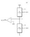
도 12는 도 1의 기판 모니터 회로(130)를 보여주는 블록도이다. 도 12를 참조하면, 기판 모니터 회로(130)는 업-트림기(131), 다운-트림기(133), 그리고 비교기(135)를 포함한다.12 is a block diagram showing the
업-트림기(131)에 기판 전압(Vsub)이 제공된다. 다운-트림기(133)는 접지 단자에 연결된다. 업-트림기(131) 및 다운-트림기(133) 사이의 중간 노드(C)는 비교기(135)에 연결된다. 업-트림기(131) 및 다운-트림기(133)는 기판 전압(Vsub)을 분배할 것이다. 예를 들면, 업-트림기(131) 및 다운-트림기(133)는 저항값을 갖도록 구성될 것이다. 즉,업-트림기(131) 및 다운-트림기(133)에 의해 분배된 기판 전압(Vsub)이 비교기(135)에 제공된다.The substrate voltage (Vsub) is provided to the up-trimmer (131). The down-
예시적으로, 업-트림기(131) 및 다운 트림기(133)는 가변 가능한 저항값을 갖도록 구성된다. 예를 들면, 업-트림기(131)는 제 1 코드 신호(CODE1)에 응답하여 저항값을 조절하도록 구성된다. 다운-트림기(133)는 제 2 코드 신호(CODE2)에 응답하여 저항값을 조절하도록 구성된다.Illustratively, the up-
비교기(135)는 중간 노드(C)의 전압 및 기준 전압(Vref)을 비교한다. 비교 결과에 따라, 비교기(135)는 접지 활성 신호(GE)를 활성화 또는 비활성화 한다. 접지 활성 신호(129)는 어드레스 디코더(120)에 전달된다. 어드레스 디코더(120)는 접지 활성 신호(GE)에 응답하여 선택 메모리 블록(예를 들면, BLKi)의 접지 선택 라인(GSL)을 구동한다. 예를 들면, 어드레스 디코더(120)는 도 9 내지 도 11을 참조하여 설명된 바와 같이 접지 선택 라인(GSL)을 구동할 것이다. 즉, 업-트림기(131) 및 다운-트림기(133)의 분배비 및 기준 전압(Vref)의 레벨에 따라, 목표 전압(Vtar)의 레벨이 설정될 것이다.The comparator 135 compares the voltage of the intermediate node C and the reference voltage Vref. According to the comparison result, the comparator 135 activates or deactivates the ground activation signal GE. The ground enable
또한, 업-트림기(131) 및 다운-트림기(133)의 분배비는 코드 신호들(CODE1, CODE2)에 따라 제어된다. 따라서, 코드 신호들(CODE1, CODE2)에 기반하여 목표 전압(Vtar)의 레벨이 가변될 수 있다.Also, the distribution ratio of the up-
도 12에서, 비교기(135)의 출력이 접지 활성 신호(GE)로 제공되는 것으로 설명되었다. 그러나, 비교기(135)의 출력을 조절하여 접지 활성 신호(GE)로 출력하는 로직 블록이 추가적으로 제공될 수 있다.In Figure 12, the output of the comparator 135 has been described as being provided as a ground enable signal GE. However, a logic block that adjusts the output of the comparator 135 and outputs it to the ground enable signal GE may be additionally provided.
도 13은 도 12의 업-트림기(131)를 보여주는 회로도이다. 도 13을 참조하면, 업-트림기(131)는 제 1 내지 제 n 저항들(R1~Rn) 및 제 1 내지 제 n 스위치들(T1~Tn)을 포함한다. 예시적으로, 제 1 내지 제 n 스위치들(T1~Tn)은 트랜지스터인 것으로 도시되어 있다. 그러나, 제 1 내지 제 n 스위치들(T1~Tn)은 트랜지스터로 한정되지 않는다.13 is a circuit diagram showing the up-
제 1 내지 제 n 저항들(R1~Rn)은 직렬 연결된다. 제 1 내지 제 n 저항들(R1~Rn) 및 제 1 내지 제 n 트랜지스터들(T1~Tn)은 각각 병렬 연결된다. 제 1 내지 제 n 트랜지스터들(T1~Tn)은 제 1 코드 신호(CODE1)에 응답하여 동작한다. 예시적으로, 제 1 트랜지스터(T1)가 턴-온 되면, 제 1 저항(R1)을 우회하는 경로가 제 1 트랜지스터(T1)에 의해 제공된다. 따라서, 업-트림기(131)의 저항값은 감소한다. 제 1 트랜지스터(T1)가 턴-오프 되면, 제 1 저항(R1)을 우회하는 경로는 제공되지 않는다. 따라서, 제 1 저항(R1)의 저항값은 업-트림기(131)의 저항값에 반영된다.The first to n-th resistors R1 to Rn are connected in series. The first to n-th resistors R1 to Rn and the first to the n-th transistors T1 to Tn are connected in parallel. The first to nth transistors T1 to Tn operate in response to the first code signal CODE1. Illustratively, when the first transistor T1 is turned on, the path bypassing the first resistor R1 is provided by the first transistor T1. Therefore, the resistance value of the up-
제 2 코드 신호(CODE2)가 제공되는 것을 제외하면, 도 12의 다운-트림기(133)는 업-트림기(131)와 마찬가지로 구성될 것이다. 따라서, 다운-트림기(133)의 상세한 설명은 생략된다.The down-
상술한 바와 같이, 제 1 코드 신호(CODE1)에 기반하여 제어함으로써, 업-트림기(131)의 저항값이 조절될 수 있다. 또한, 제 2 코드 신호(CODE2)를 제어함으로써 다운-트림기(1330의 저항값이 조절될 수 있다. 따라서, 제 1 코드 신호(CODE1) 및 제 2 코드 신호(CODE2)를 제어함으로써 목표 전압(Vtar)의 레벨이 가변될 수 있다.As described above, by controlling based on the first code signal CODE1, the resistance value of the up-
도 14A는 도 1의 불휘발성 메모리 장치의 메모리 셀 어레이(110) 및 어드레스 디코더(120)를 보여주는 블록도이다. 예시적으로, 메모리 셀 어레이(110)의 하나의 메모리 블록(BLKi)이 도시되어 있다.14A is a block diagram showing a
도 14A를 참조하면, 어드레스 디코더(120)는 블록 선택 회로(121), 블록 워드 라인 구동기(123), 스트링 선택 라인 구동기(125), 워드 라인 구동기(127), 그리고 접지 선택 라인 구동기(129)를 포함한다.14A, the
블록 선택 회로(121)는 메모리 셀 어레이(110)의 메모리 블록들(BLK1~BLKi) 중 하나를 선택하도록 구성된다. 블록 선택 회로(121)는 복수의 스위치들을 포함한다. 예시적으로, 블록 선택 회로(121)는 복수의 트랜지스터들을 포함할 것이다. 예시적으로, 블록 선택 회로(121)는 복수의 고전압 트랜지스터들을 포함할 것이다.The
블록 선택 회로(121)의 트랜지스터들의 게이트는 블록 워드 라인(BLKWL)에 공통으로 연결된다. 블록 선택 회로(121)의 트랜지스터들 중 일부는 스트링 선택 라인들(SSL1~SSL3) 및 선택 라인들(SS1~SS3) 사이에 각각 연결된다. 블록 선택 회로(121)의 트랜지스터들 중 일부는 워드 라인들(WL1~WL7) 및 선택 라인들(S1~S7) 사이에 각각 연결된다. 블록 선택 회로(121)의 트랜지스터들 중 일부는 접지 선택 라인(GSL) 및 선택 라인(GS) 사이에 연결된다. 즉, 블록 워드 라인(BLKWL)의 전압 레벨에 응답하여, 블록 선택 회로(121)는 스트링 선택 라인들(SSL1~SSL3), 워드 라인들(WL1~WL7), 그리고 접지 선택 라인(GSL)을 각각 스트링 선택 라인 구동기(125), 워드 라인 구동기(127), 그리고 접지 선택 라인 구동기(129)에 연결한다.The gates of the transistors of the
블록 워드 라인 구동기(123)는 블록 워드 라인(BLKWL)을 구동하도록 구성된다. 예를 들면, 메모리 블록(BLKi)이 선택될 때, 블록 워드 라인 구동기(123)는 블록 워드 라인(BLKWL)에 선택 전압을 인가할 것이다. 예시적으로, 프로그램 동작 및 읽기 동작 시에, 블록 워드 라인 구동기(123)는 블록 워드 라인(BLKWL)에 고전압(Vpp)을 인가할 것이다. 예시적으로, 소거 동작 시에, 블록 워드 라인 구동기(123)는 블록 워드 라인(BLKWL)에 전원 전압(Vcc)을 인가할 것이다.The block
스트링 선택 라인 구동기(125)는 선택 라인들(SS1~SS3)에 연결된다. 선택 라인들(SS1~SS3)은 블록 선택 회로(121)를 통해 스트링 선택 라인들(SSL1~SSL3)에 연결된다. 즉, 스트링 선택 라인 구동기(125)는 블록 선택 회로(121)를 통해 스트링 선택 라인들(SSL1~SSL3)을 구동하도록 구성된다. 예를 들면, 소거 동작 시에, 스트링 선택 라인 구동기(125)는 스트링 선택 라인들(SSL1~SSL3)을 플로팅하도록 구성된다.The string
워드 라인 구동기(127)는 선택 라인들(S1~S7)에 연결된다. 선택 라인들(S1~S7)은 블록 선택 회로(121)를 통해 워드 라인들(WL1~WL7)에 연결된다. 즉, 워드 라인 구동기(127)는 블록 선택 회로(121)를 통해 워드 라인들(WL1~WL7)을 구동하도록 구성된다. 예시적으로, 소거 동작 시에, 워드 라인 구동기(127)는 워드 라인들(WL1~WL7)에 워드 라인 소거 전압(Vwe)을 인가하도록 구성된다.The
접지 선택 라인 구동기(129)는 선택 라인(GS)에 연결된다. 선택 라인(GS)은 블록 선택 회로(121)를 통해 접지 선택 라인(GSL)에 연결된다. 즉, 접지 선택 라인 구동기(129)는 블록 선택 회로(121)를 통해 접지 선택 라인(GSL)을 구동하도록 구성된다.The ground
소거 동작 시에, 접지 선택 라인 구동기(129)는 접지 활성 신호(GE)에 응답하여 동작하도록 구성된다. 예시적으로, 소거 동작이 시작될 때, 접지 선택 라인 구동기(129)는 접지 선택 라인(GSL)에 미리 설정된 전압(Vpd)을 인가하도록 구성된다. 미리 설정된 전압(Vpd)은 접지 선택 라인(GSL)에 연결된 접지 선택 트랜지스터(GST)를 턴-오프 하는 전압일 것이다. 접지 활성 신호(GE)의 논리값이 천이할 때, 접지 선택 라인 구동기(129)는 접지 선택 라인(GSL)을 플로팅하도록 구성된다.In the erase operation, the ground
예를 들면, 접지 활성 신호(GE)가 천이할 때, 접지 선택 라인 구동기(129)는 접지 선택 라인(GSL)이 플로팅되도록 출력을 제어한다. 예를 들면, 접지 활성 신호(GE)는 블록 워드 라인(BLKWL)의 전압 레벨과 같은 레벨을 갖는 전압을 출력할 것이다. 예를 들면, 소거 동작 시에 블록 워드 라인(BLKWL)에 전원 전압(Vcc)이 인가되면, 접지 활성 신호(GE)의 천이에 응답하여 접지 선택 라인 구동기(129)는 전원 전압(Vcc)을 출력할 것이다. 이때, 접지 선택 라인(GSL)에 대응하는 블록 선택 회로(121)의 트랜지스터의 게이트 전압 및 드레인(또는 소스) 전압이 같아질 것이다. 따라서, 접지 선택 라인(GSL)에 대응하는 블록 선택 회로(121)의 트랜지스터가 턴-오프될 것이다. 즉, 접지 선택 라인(GSL)이 플로팅될 것이다.For example, when the ground activation signal GE transits, the ground
접지 활성 신호(GE)가 천이할 때, 접지 선택 라인 구동기(129)는 블록 워드 라인(BLKWL)의 전압 레벨과 갖은 레벨을 갖는 전압을 출력하는 것으로 한정되지 않는다. 또한, 접지 활성 신호(GE)가 천이할 때, 접지 선택 라인 구동기(129)는 전원 전압(Vcc)을 출력하는 것으로 한정되지 않는다. 예시적으로, 접지 활성 신호(GE)가 천이할 때, 접지 선택 라인 구동기(129)는, 접지 선택 라인(GSL)에 대응하는 블록 선택 회로(121)의 트랜지스터가 턴-오프 되는 전압을 출력하도록 구성될 것이다. 예시적으로, 접지 활성 신호(GE)가 천이할 때, 접지 선택 라인 구동기(129)는 출력 노드를 플로팅하도록 구성될 수 있다.When the ground activation signal GE transits, the ground
상술한 바와 같이, 본 발명의 실시 예에 따른 불휘발성 메모리 장치(100)는 소거 동작 시에 메모리 셀 어레이(110)의 기판 전압의 변화에 따라 접지 선택 라인(GSL)을 구동하도록 구성된다. 따라서, 메모리 셀들(MC1~MC7)의 소거 교란이 방지되며, 접지 선택 트랜지스터(GST)의 소거가 방지된다. 즉, 불휘발성 메모리 장치(100)의 신뢰성이 향상된다.As described above, the
상술된 바와 같이, 본 발명의 실시 예에 따른 불휘발성 메모리 장치(100)는 메모리 셀 어레이(110)의 각 메모리 블록(BLKi)에 대응하는 블록 선택 회로(121), 블록 워드 라인 구동기(123), 스트링 선택 라인 구동기(125), 워드 라인 구동기(127), 그리고 접지 선택 라인 구동기(129)를 포함한다. 불휘발성 메모리 장치는 소거 동작 시에 메모리 셀 어레이(110)의 기판 전압의 변화에 따라 접지 선택 라인(GSL)을 구동한다. 따라서, 메모리 셀들(MC1~MC7)의 소거 교란이 방지되고, 접지 선택 트랜지스터(GST)가 소거되는 것이 방지된다. 즉, 불휘발성 메모리 장치(100)의 신뢰성이 향상된다.The
도 14B는 도 1의 불휘발성 메모리 장치(100)의 메모리 셀 어레이(110) 및 어드레스 디코더(120)의 다른 예를 보여주는 블록도이다. 예시적으로, 메모리 셀 어레이(110)의 메모리 블록들(BLK0, BLK1)이 도시되어 있다.14B is a block diagram showing another example of the
도 14B를 참조하면, 도 14A에 도시된 어드레스 디코더(120)와 달리, 어드레스 디코더(120')는 각 메모리 블록들(BLK0, BLK1)에 대응하는 블록 선택 회로들(1210, 1211)과 블록 워드 라인 구동기들(1230, 1231), 모든 메모리 블록들(BLKn)에 대응하는 하나의 공통 소스 라인 구동기(125), 워드 라인 구동기(127), 그리고 접지 선택 라인 구동기(129)를 포함한다.14B, unlike the
블록 선택 회로들(121n)은 대응하는 블록 워드 라인 구동기(123n)로부터 전송되는 블록 워드 라인 신호(BLKWL)에 응답하여, 스트링 선택 라인 구동기(125), 워드 라인 구동기(127), 그리고 접지 선택 라인 구동기(129)로부터의 전압을 전달한다. 블록 선택 회로(121n)는 복수의 스위치들을 포함한다. 예시적으로, 블록 선택 회로(121n)는 복수의 트랜지스터들을 포함할 수 있다. 예시적으로, 블록 선택 회로(121n)는 복수의 고전압 트랜지스터들을 포함할 수 있다.The block
블록 선택 회로(121n)의 트랜지스터들의 게이트는 블록 워드 라인(BLKWL)에 공통으로 연결된다. 블록 선택 회로(121n)의 트랜지스터들 중 일부는 스트링 선택 라인들(SSL0~SSL2) 및 선택 라인들(SS0~SS2) 사이에 각각 연결된다. 블록 선택 회로(121n)의 트랜지스터들 중 일부는 워드 라인들(WL0~WL15) 및 선택 라인들(S0~S15) 사이에 각각 연결된다. 블록 선택 회로(121n)의 트랜지스터들 중 일부는 접지 선택 라인들(GSL0, GSL1) 및 선택 라인들(GS0, GS1) 사이에 연결된다. 즉, 블록 워드 라인(BLKWL)의 전압 레벨에 응답하여, 블록 선택 회로(121n)는 스트링 선택 라인들(SSL0~SSL2), 워드 라인들(WL0~WL15), 그리고 접지 선택 라인들(GSL0, GSL1)을 각각 스트링 선택 라인 구동기(125), 워드 라인 구동기(127), 그리고 접지 선택 라인 구동기(129)에 연결한다.The gates of the transistors of the
블록 워드 라인 구동기(123n)는 블록 워드 라인(BLKWL)을 구동하도록 구성된다. 예를 들면, 메모리 블록(BLK0)이 선택될 때, 블록 워드 라인 구동기(1230)는 블록 워드 라인(BLKWL)에 선택 전압을 인가할 것이다. 예시적으로, 프로그램 동작 및 읽기 동작 시에, 블록 워드 라인 구동기(1230)는 블록 워드 라인(BLKWL)에 고전압(Vpp)을 인가할 것이다. 예시적으로, 소거 동작 시에, 블록 워드 라인 구동기(1230)는 블록 워드 라인(BLKWL)에 전원 전압(Vcc)을 인가할 것이다.The block
스트링 선택 라인 구동기(125)는 선택 라인들(SS1~SS3)에 연결된다. 선택 라인들(SS0~SS2)은 블록 선택 회로(121n)를 통해 스트링 선택 라인들(SSL0~SSL2)에 연결된다. 즉, 스트링 선택 라인 구동기(125)는 블록 선택 회로(121n)를 통해 스트링 선택 라인들(SSL0~SSL2)을 구동하도록 구성된다. 예를 들면, 소거 동작 시에, 스트링 선택 라인 구동기(125)는 스트링 선택 라인들(SSL0~SSL2)을 플로팅하도록 구성된다.The string
워드 라인 구동기(127)는 선택 라인들(S0~S15)에 연결된다. 선택 라인들(S0~S15)은 블록 선택 회로(121n)를 통해 워드 라인들(WL0~WL15)에 연결된다. 즉, 워드 라인 구동기(127)는 블록 선택 회로(121n)를 통해 워드 라인들(WL0~WL15)을 구동하도록 구성된다. 예시적으로, 소거 동작 시에, 워드 라인 구동기(127)는 워드 라인들(WL0~WL15)에 워드 라인 소거 전압(Vwe)을 인가하도록 구성된다.The
접지 선택 라인 구동기(129)는 접지 선택 라인 구동기(129)는 선택 라인들(GS0, GS1)에 연결된다. 선택 라인들(GS0, GS1)은 블록 선택 회로(121n)를 통해 접지 선택 라인들(GSL0, GSL1)에 연결된다. 즉, 접지 선택 라인 구동기(129)는 블록 선택 회로(121n)를 통해 접지 선택 라인들(GSL0, GSL1)을 구동하도록 구성된다.The ground
소거 동작 시에, 접지 선택 라인 구동기(129)는 접지 활성 신호(GE)에 응답하여 동작하도록 구성된다. 예시적으로, 소거 동작이 시작될 때, 접지 선택 라인 구동기(129)는 접지 선택 라인들(GSL0, GSL1)에 미리 설정된 전압(Vpd)을 인가하도록 구성된다. 미리 설정된 전압(Vpd)은 접지 선택 라인들(GSL0, GSL1)에 연결된 접지 선택 트랜지스터들(GST)을 턴-오프 하는 전압일 것이다. 접지 활성 신호(GE)의 논리값이 천이할 때, 접지 선택 라인 구동기(129)는 접지 선택 라인들(GSL0, GSL1)을 플로팅하도록 구성된다.In the erase operation, the ground
예를 들면, 접지 활성 신호(GE)가 천이할 때, 접지 선택 라인 구동기(129)는 접지 선택 라인들(GSL0, GSL1)이 플로팅되도록 출력을 제어한다. 예를 들면, 접지 활성 신호(GE)는 블록 워드 라인(BLKWL)의 전압 레벨과 같은 레벨을 갖는 전압을 출력할 것이다. 예를 들면, 소거 동작 시에 블록 워드 라인(BLKWL)에 전원 전압(Vcc)이 인가되면, 접지 활성 신호(GE)의 천이에 응답하여 접지 선택 라인 구동기(129)는 전원 전압(Vcc)을 출력할 것이다. 이때, 접지 선택 라인들(GSL0, GSL1)에 대응하는 블록 선택 회로(121n)의 트랜지스터의 게이트 전압 및 드레인(또는 소스) 전압이 같아질 것이다. 따라서, 접지 선택 라인들(GSL0, GSL1)에 대응하는 블록 선택 회로(121n)의 트랜지스터가 턴-오프될 것이다. 즉, 접지 선택 라인들(GSL0, GSL1)이 플로팅될 것이다.For example, when the ground activation signal GE transitions, the ground
접지 활성 신호(GE)가 천이할 때, 접지 선택 라인 구동기(129)는 블록 워드 라인(BLKWL)의 전압 레벨과 갖은 레벨을 갖는 전압을 출력하는 것으로 한정되지 않는다. 또한, 접지 활성 신호(GE)가 천이할 때, 접지 선택 라인 구동기(129)는 전원 전압(Vcc)을 출력하는 것으로 한정되지 않는다. 예시적으로, 접지 활성 신호(GE)가 천이할 때, 접지 선택 라인 구동기(129)는, 접지 선택 라인들(GSL0, GSL1)에 대응하는 블록 선택 회로(121)의 트랜지스터가 턴-오프 되는 전압을 출력하도록 구성될 것이다. 예시적으로, 접지 활성 신호(GE)가 천이할 때, 접지 선택 라인 구동기(129)는 출력 노드를 플로팅하도록 구성될 수 있다.When the ground activation signal GE transits, the ground
상술된 바와 같이, 어드레스 디코더(120')는 각 메모리 블록들(BLK0, BLK1)에 대응하는 블록 선택 회로들(1210, 1211)과 블록 워드 라인 구동기들(1230, 1231), 그리고 모든 메모리 블록들(BLKn)에 대응하는 하나의 공통 소스 라인 구동기(125), 워드 라인 구동기(127), 그리고 접지 선택 라인 구동기(129)를 포함한다. 상술된 바와 같이, 본 발명의 실시 예에 따른 불휘발성 메모리 장치(100)는 소거 동작 시에 메모리 셀 어레이(110)의 기판 전압의 변화에 따라 접지 선택 라인들(GSL0, GSL1)을 구동하도록 구성된다. 따라서, 메모리 셀들(MC)의 소거 교란이 방지되며, 접지 선택 트랜지스터(GST)의 소거가 방지된다. 즉, 불휘발성 메모리 장치(100)의 신뢰성이 향상된다.As described above, the address decoder 120 'includes
도 15는 도 3 내지 도 5를 참조하여 설명된 메모리 블록(BLKi)의 등가 회로의 제 1 응용 예를 보여주는 회로도이다. 도 6을 참조하여 설명된 등가 회로와 비교하면, 메모리 블록(BLKi_1)의 각 낸드 스트링(NS)에 측면 트랜지스터(LTR)가 추가적으로 제공된다. 측면 트랜지스터(LTR)는 접지 선택 트랜지스터(GST) 및 공통 소스 라인 사이(CSL)에 연결된다. 측면 트랜지스터(LTR)의 게이트(또는 제어 게이트)는 접지 선택 트랜지스터(GST)의 게이트(또는 제어 게이트)와 함께 접지 선택 라인(GSL)에 연결된다.Fig. 15 is a circuit diagram showing a first application example of an equivalent circuit of the memory block BLKi described with reference to Figs. 3 to 5. Fig. Compared with the equivalent circuit described with reference to Fig. 6, a lateral transistor LTR is additionally provided in each NAND string NS of the memory block BLKi_1. The side transistor LTR is connected to the ground selection transistor GST and the common source line CSL. The gate (or control gate) of the lateral transistor LTR is connected to the ground selection line GSL together with the gate (or control gate) of the ground selection transistor GST.
도 3 내지 도 6에 도시된 바와 같이, 기판(111)에 인접한 제 1 도전 물질들(211, 212, 213)은 접지 선택 라인(GSL)에 대응한다. 제 1 도전 물질들(211, 212, 213)에 미리 설정된 전압이 인가되면, 제 2 방향의 바디(114) 중 제 1 도전 물질들(211, 212, 213)에 대응하는 영역에 채널이 형성된다. 또한, 제 1 도전 물질들(211, 212, 213)에 미리 설정된 전압이 인가되면, 기판(111)에서 제 1 도전 물질들(211, 212, 213)에 인접한 영역에 채널이 형성된다.As shown in FIGS. 3-6, the first
제 1 도핑 영역(311)은 제 1 도전 물질(211)의 전압에 의해 형성된 기판(111)의 패널에 연결된다. 제 1 도전 물질(211)의 전압에 의해 형성된 기판(111)의 채널은 제 1 도전 물질(211)의 전압에 의해 제 2 방향의 바디로 동작하는 표면층(114)에 형성된 채널과 연결된다.The first
마찬가지로, 제 1 도전 물질들(211, 212, 213)의 전압에 의해 형성된 기판(111)에 채널들이 형성된다. 제 1 내지 제 4 도핑 영역들(311~314)은 각각 제 1 도전 물질들(211, 212, 213)의 전압에 의해 기판(111)에 형성된 채널들을 통해 제 2 방향의 바디로 동작하는 표면층(114)에 연결된다.Likewise, channels are formed in the
도 3 내지 도 6을 참조하여 설명된 바와 같이, 제 1 내지 제 4 도핑 영역들(311~314)은 공통 소스 라인(CSL)을 구성한다. 공통 소스 라인(CSL) 메모리 셀들(MC1~MC7)의 채널은 접지 선택 라인(GSL)의 전압에 의해 형성되는 기판에 수직한 채널 및 기판에 평행한 채널을 통해 전기적으로 연결된다.As described with reference to Figs. 3 to 6, the first to fourth
즉, 공통 소스 라인(CSL) 및 제 1 메모리 셀들(MC1) 사이에, 접지 선택 라인(GSL)에 의해 구동되며 기판에 수직한 트랜지스터 및 기판과 평행한 트랜지스터가 동작하는 것으로 이해될 수 있다. 기판에 수직한 트랜지스터는 도 15에 도시된 접지 선택 트랜지스터(GST)로 이해될 수 있으며, 기판에 평향한 트랜지스터는 도 15에 도시된 측면 트랜지스터(LTR)로 이해될 수 있다.That is, it can be understood that between the common source line CSL and the first memory cells MC1, a transistor which is driven by the ground selection line GSL and is parallel to the substrate and parallel to the substrate operates. The transistor vertical to the substrate can be understood as the ground selection transistor (GST) shown in Fig. 15, and the transistor flattened to the substrate can be understood as the lateral transistor (LTR) shown in Fig.
도 16은 도 3 내지 도 5를 참조하여 설명된 메모리 블록(BLKi)의 등가 회로의 제 2 응용 예를 보여주는 회로도이다. 도 6의 메모리 블록(BLKi)과 비교하면, 각 낸드 스트링(NS)에서, 메모리 셀들(MC1~MC6)과 공통 소스 라인(CSL) 사이에 제 1 및 제 2 접지 선택 트랜지스터들(GST1, GST2)이 제공된다. 즉, 제 1 도전 물질들(211~291, 212~292, 213~293) 중 접지 선택 라인들(GSL1, GSL2) 및 접지 선택 트랜지스터들(GST)로 사용되는 도전 물질들의 수가 가변될 수 있다.Fig. 16 is a circuit diagram showing a second application example of the equivalent circuit of the memory block BLKi described with reference to Figs. 3 to 5. Fig. Compared with the memory block BLKi in FIG. 6, in each NAND string NS, the first and second ground selection transistors GST1 and GST2 are connected between the memory cells MC1 to MC6 and the common source line CSL, / RTI > That is, the number of conductive materials used as the ground selection lines GSL1 and GSL2 and the ground selection transistors GST among the first
동일한 높이의 접지 선택 트랜지스터(GST1 또는 GST2)에 대응하는 접지 선택 라인들(GSL1, GSL2)은 공통으로 연결될 수 있다. 동일한 낸드 스트링(NS)에 대응하는 접지 선택 라인들(GSL1, GSL2)은 공통으로 연결될 수 있다. 또한, 상이한 높이의 접지 선택 라인들(GSL1, GSL2)은 공통으로 연결될 수 있다.The ground selection lines GSL1 and GSL2 corresponding to the ground selection transistors GST1 and GST2 of the same height can be connected in common. The ground selection lines GSL1 and GSL2 corresponding to the same NAND string NS can be connected in common. In addition, the ground selection lines GSL1 and GSL2 of different heights can be connected in common.
도 17은 도 3 내지 도 5를 참조하여 설명된 메모리 블록(BLKi)의 등가 회로의 제 3 응용 예를 보여주는 회로도이다. 도 16의 메모리 블록(BLKi_2)과 비교하면, 각 낸드 스트링(NS)에서, 메모리 셀들(MC1~MC5) 및 비트 라인(BL) 사이에 제 1 및 제 2 스트링 선택 트랜지스터들(SST1, SST2)이 제공된다. 즉, 제 1 도전 물질들(211~291, 212~292, 213~293) 중 스트링 선택 라인(SSL) 및 스트링 선택 트랜지스터들(SST)로 사용되는 도전 물질들의 수가 가변될 수 있다.17 is a circuit diagram showing a third application example of the equivalent circuit of the memory block BLKi described with reference to Figs. 3 to 5. Fig. Compared with the memory block BLKi_2 in FIG. 16, in each NAND string NS, the first and second string selection transistors SST1 and SST2 are connected between the memory cells MC1 to MC5 and the bit line BL / RTI > That is, the number of conductive materials used as the string selection line SSL and the string selection transistors SST among the first
도 18은 도 3 내지 도 5를 참조하여 설명된 메모리 블록(BLKi)의 등가 회로의 제 4 응용 예를 보여주는 회로도이다. 도 17의 메모리 블록(BLKi_3)과 비교하면, 메모리 블록(BLKi_4)의 동일한 낸드 스트링(NS)에 대응하는 스트링 선택 라인들(SSL)은 공통으로 연결된다.Fig. 18 is a circuit diagram showing a fourth application example of the equivalent circuit of the memory block BLKi described with reference to Figs. 3 to 5. Fig. Compared with the memory block BLKi_3 in Fig. 17, the string selection lines SSL corresponding to the same NAND string NS of the memory block BLKi_4 are connected in common.
상술된 바와 같이, 메모리 블록(BLKi)의 각 낸드 스트링(NS)에 적어도 하나의 접지 선택 트랜지스터(GST) 및 적어도 하나의 스트링 선택 트랜지스터(SST)가 제공될 수 있다. 적어도 하나의 접지 선택 트랜지스터(GST)는 적어도 하나의 접지 선택 라인(GSL)에 연결되고, 적어도 하나의 스트링 선택 트랜지스터(SST)는 적어도 하나의 스트링 선택 라인(SSL)에 연결될 것이다.As described above, at least one ground selection transistor GST and at least one string selection transistor SST may be provided for each NAND string NS of the memory block BLKi. At least one ground select transistor (GST) is coupled to at least one ground select line (GSL), and at least one string select transistor (SST) is coupled to at least one string select line (SSL).
동일한 높이의 접지 선택 라인들(GSL)은 공통으로 연결될 수 있다. 또한, 상이한 높이의 접지 선택 라인들(GSL)은 공통으로 연결될 수 있다. 그리고, 상이한 높이의 스트링 선택 라인들(SSL)은 공통으로 연결될 수 있다.The ground selection lines GSL of the same height can be connected in common. In addition, the ground selection lines GSL of different heights can be connected in common. And, string selection lines (SSL) of different heights can be connected in common.
도 19는 도 3 내지 도 5를 참조하여 설명된 메모리 블록(BLKi)의 등가 회로의 제 5 응용 예(BLKi_5)를 보여주는 회로도이다. 도 6의 메모리 블록(BLKi)과 비교하면, 메모리 블록(BLKi_5)의 각 낸드 스트링(NS)에서 스트링 선택 트랜지스터(SST)와 더미 메모리 셀(DMC3)이 제공된다. 더미 메모리 셀들(DMC3)은 스트링 선택 라인들(SSL1, SSL2, SSL3)과 인접한 더미 워드 라인(DWL3)에 공통으로 연결된다. 즉, 제 1 도전 물질들(211~291, 212~292, 213~293) 중 더미 워드 라인(DWL) 및 더미 메모리 셀(DMC)로 사용되는 제 1 도전 물질들의 수가 가변될 수 있다.Fig. 19 is a circuit diagram showing a fifth application example (BLKi_5) of an equivalent circuit of the memory block BLKi described with reference to Figs. 3 to 5. Fig. Compared with the memory block BLKi in Fig. 6, the string selection transistor SST and the dummy memory cell DMC3 are provided in each NAND string NS of the memory block BLKi_5. The dummy memory cells DMC3 are connected in common to the string selection lines SSL1, SSL2 and SSL3 and the adjacent dummy word lines DWL3. That is, the number of the first conductive materials used as the dummy word line DWL and the dummy memory cell DMC among the first
도 20은 도 3 내지 도 5를 참조하여 설명된 메모리 블록(BLKi)의 등가 회로의 제 6 응용 예를 보여주는 회로도이다. 도 6의 메모리 블록(BLKi)과 비교하면, 메모리 블록(BLKi_6)의 각 낸드 스트링(NS)에서 접지 선택 트랜지스터(GST)와 인접한 더미 메모리 셀(DMC1)이 제공된다. 더미 메모리 셀들(DMC1)은 접지 선택 라인(GSL)과 인접한 더미 워드 라인(DWL1)에 공통으로 연결된다. 즉, 제 1 도전 물질들(211~291, 212~292, 213~293) 중 더미 워드 라인(DWL) 및 더미 메모리 셀(DMC)로 사용되는 제 1 도전 물질들의 수가 가변될 수 있다.20 is a circuit diagram showing a sixth application example of the equivalent circuit of the memory block BLKi described with reference to Figs. 3 to 5. Fig. Compared with the memory block BLKi of Fig. 6, the dummy memory cell DMC1 adjacent to the ground selection transistor GST is provided at each NAND string NS of the memory block BLKi_6. The dummy memory cells DMC1 are connected in common to the ground selection line GSL and the adjacent dummy word line DWL1. That is, the number of the first conductive materials used as the dummy word line DWL and the dummy memory cell DMC among the first
도 21은 도 3 내지 도 5를 참조하여 설명된 메모리 블록(BLKi)의 등가 회로의 제 7 응용 예(BLKi_7)를 보여주는 회로도이다. 도 6의 메모리 블록(BLKi)과 비교하면, 메모리 블록(BLKi_7)의 각 낸드 스트링(NS)에서 접지 선택 트랜지스터(GST)와 인접한 더미 메모리 셀(DMC1), 그리고 스트링 선택 트랜지스터(SST)와 인접한 더미 메모리 셀(DMC3)이 제공된다.21 is a circuit diagram showing a seventh application example (BLKi_7) of an equivalent circuit of the memory block BLKi described with reference to Figs. 3 to 5. Fig. Compared with the memory block BLKi in Fig. 6, the dummy memory cell DMC1 adjacent to the ground selection transistor GST and the dummy memory cell DMC1 adjacent to the string selection transistor SST in each NAND string NS of the memory block BLKi_7, A memory cell DMC3 is provided.
접지 선택 트랜지스터(GST)와 인접한 더미 메모리 셀(DMC1)은 접지 선택 라인(GSL)과 인접한 더미 워드 라인(DWL1)에 공통으로 연결된다. 스트링 선택 트랜지스터(SST)와 인접한 더미 메모리 셀(DMC3)은 스트링 선택 라인들(SSL1, SSL2, SSL3)과 인접한 더미 워드 라인(DWL3)에 공통으로 연결된다. 즉, 제 1 도전 물질들(211~291, 212~292, 213~293) 중 더미 워드 라인(DWL) 및 더미 메모리 셀(DMC)로 사용되는 제 1 도전 물질들의 수가 가변될 수 있다.The dummy memory cell DMC1 adjacent to the ground selection transistor GST is connected in common to the ground selection line GSL and the adjacent dummy word line DWL1. The dummy memory cell DMC3 adjacent to the string selection transistor SST is connected in common to the string selection lines SSL1, SSL2 and SSL3 and the adjacent dummy word line DWL3. That is, the number of the first conductive materials used as the dummy word line DWL and the dummy memory cell DMC among the first
상술한 바와 같이, 메모리 블록(BLKi)의 각 낸드 스트링(NS)에 접지 선택 트랜지스터(GST)와 인접한 적어도 하나의 더미 메모리 셀(DMC)이 제공될 수 있다. 그리고, 메모리 블록(BLKi)의 각 낸드 스트링(NS)에 스트링 선택 트랜지스터(GST)와 인접한 적어도 하나의 더미 메모리 셀(DMC)이 제공될 수 있다. 더미 메모리 셀(DMC)은 더미 워드 라인(DWL)에 연결된다. 동일한 높이의 더미 워드 라인들(DWL)은 공통으로 연결될 것이다.As described above, at least one dummy memory cell DMC adjacent to the ground selection transistor GST may be provided for each NAND string NS of the memory block BLKi. Each NAND string NS of the memory block BLKi may be provided with at least one dummy memory cell DMC adjacent to the string selection transistor GST. The dummy memory cell DMC is connected to the dummy word line DWL. The dummy word lines DWL of the same height will be connected in common.
도 22는 도 2의 메모리 블록(BLKi)의 다른 실시 예를 보여주는 블록도이다. 도 3의 메모리 블록(BLKi)과 비교하면, 메모리 블록(BLKi')에서, 필라들(113')은 사각 기둥의 형태로 제공될 것이다. 또한, 제 1 방향을 따라 배치된 필라들(113') 사이에, 절연 물질들(101)이 제공된다.22 is a block diagram showing another embodiment of the memory block BLKi of FIG. Compared with the memory block BLKi in FIG. 3, in the memory block BLKi ', the pillars 113' will be provided in the form of a quadratic pole. Further, between the pillars 113 'arranged along the first direction, insulating
예시적으로, 절연 물질들(101)은 제 2 방향을 따라 신장되어 기판(111)에 연결될 것이다. 또한, 절연 물질들(101)은 필라들(113')이 제공되는 영역을 제외한 영역에서 제 1 방향을 따라 신장될 것이다. 즉, 도 3을 참조하여 설명된 제 1 도전 물질들(211~291, 212~292, 213~293))은 절연 물질들(101)에 의해 제 1 부분들(211a~291a, 212a~292a, 213a~293a) 및 제 2 부분들(211b~291b, 212b~292b, 213b~293b)로 분리될 것이다.Illustratively, the insulating
제 1 및 제 2 도핑 영역들(311, 312) 상의 영역에서, 각 필라(113')는 제 1 도전 물질들의 제 1 부분들(211a~291a) 및 절연막(116)과 하나의 낸드 스트링(NS)을 형성하고, 제 1 도전 물질들의 제 2 부분들(211b~291b) 및 절연막(116)과 다른 하나의 낸드 스트링(NS)을 형성할 것이다.In the region on the first and second
제 2 및 제 3 도핑 영역들(312, 313) 상의 영역에서, 각 필라(113')는 제 1 도전 물질들의 제 1 부분들(212a~292a) 및 절연막(116)과 하나의 낸드 스트링(NS)을 형성하고, 제 1 도전 물질들의 제 2 부분들(212b~292b) 및 절연막(116)과 다른 하나의 낸드 스트링(NS)을 형성할 것이다.In the region on the second and third
제 3 및 제 4 도핑 영역들(313, 314) 상의 영역에서, 각 필라(113')는 제 1 도전 물질들의 제 1 부분들(213a~293a) 및 절연막(116)과 하나의 낸드 스트링(NS)을 형성하고, 제 1 도전 물질들의 제 2 부분들(213b~293b) 및 절연막(116)과 다른 하나의 낸드 스트링(NS)을 형성할 것이다.In the region on the third and
즉, 절연물질(101)을 이용하여 각 필라(113')의 양 측면에 제공되는 제 1 도전 물질들의 제 1 및 제 2 부분들(211a~291a, 211b~291b)을 분리함으로써, 각 필라(113')는 두 개의 낸드 스트링(NS)을 형성할 수 있다.That is, by separating the first and
도 22를 참조하여 설명된 메모리 블록(BLKi')의 I-I'선에 따른 단면도는 도 4에 도시된 바와 같다. 따라서, 메모리 블록(BLKi')의 단면도에 대한 도면 및 상세한 설명은 생략된다.A cross-sectional view taken along line I-I 'of the memory block BLKi' described with reference to FIG. 22 is as shown in FIG. Therefore, a drawing and a detailed description of a cross-sectional view of the memory block BLKi 'are omitted.
도 23은 도 1의 불휘발성 메모리 장치(100)를 포함하는 메모리 시스템(1000)을 보여주는 블록도이다. 도 23을 참조하면, 메모리 시스템(1000)은 불휘발성 메모리 장치(1100) 및 컨트롤러(1200)를 포함한다.23 is a block diagram illustrating a
불휘발성 메모리 장치(1100)는 도 1 내지 도 22를 참조하여 설명된 바와 같이 동작하도록 구성된다. 예를 들면, 소거 동작 시에, 불휘발성 메모리 장치(1100)는 접지 선택 라인(GSL)에 미리 설정된 전압을 인가한다. 불휘발성 메모리 장치(1100)의 기판(111)의 전압 변화에 따라, 불휘발성 메모리 장치(1100)는 접지 선택 라인(GSL)을 플로팅하도록 구성된다. 따라서, 소거 교란이 방지되며 불휘발성 메모리 장치(1100) 및 불휘발성 메모리 장치(1100)를 포함하는 메모리 시스템(1000)의 신뢰성이 향상된다.The
컨트롤러(1200)는 호스트(Host) 및 불휘발성 메모리 장치(1100)에 연결된다. 호스트(Host)로부터의 요청에 응답하여, 컨트롤러(1200)는 불휘발성 메모리 장치(1100)를 액세스하도록 구성된다. 예를 들면, 컨트롤러(1200)는 불휘발성 메모리 장치(1100)의 읽기, 쓰기, 소거, 그리고 배경(background) 동작을 제어하도록 구성된다. 컨트롤러(1200)는 불휘발성 메모리 장치(1100) 및 호스트(Host) 사이에 인터페이스를 제공하도록 구성된다. 컨트롤러(1200)는 불휘발성 메모리 장치(1100)를 제어하기 위한 펌웨어(firmware)를 구동하도록 구성된다.The
예시적으로, 컨트롤러(1200)는 램(RAM, Random Access Memory), 프로세싱 유닛(processing unit), 호스트 인터페이스(host interface), 그리고 메모리 인터페이스(memory interface)와 같은 잘 알려진 구성 요소들을 더 포함한다. 램(RAM)은 프로세싱 유닛의 동작 메모리, 불휘발성 메모리 장치(1100) 및 호스트(Host) 사이의 캐시 메모리, 그리고 불휘발성 메모리 장치(1100) 및 호스트(Host) 사이의 버퍼 메모리 중 적어도 하나로서 이용된다. 프로세싱 유닛은 컨트롤러(1200)의 제반 동작을 제어한다.Illustratively,
호스트 인터페이스는 호스트(Host) 및 컨트롤러(1200) 사이의 데이터 교환을 수행하기 위한 프로토콜을 포함한다. 예시적으로, 호스트 인터페이스는 USB (Universal Serial Bus) 프로토콜, MMC (multimedia card) 프로토콜, PCI (peripheral component interconnection) 프로토콜, PCI-E (PCI-express) 프로토콜, ATA (Advanced Technology Attachment) 프로토콜, Serial-ATA 프로토콜, Parallel-ATA 프로토콜, SCSI (small computer small interface) 프로토콜, ESDI (enhanced small disk interface) 프로토콜, 그리고 IDE (Integrated Drive Electronics) 프로토콜 등과 같은 다양한 인터페이스 프로토콜들 중 적어도 하나를 통해 외부(호스트)와 통신하도록 구성된다.The host interface includes a protocol for performing data exchange between the host (Host) and the
메모리 시스템(1000)은 오류 정정 블록을 추가적으로 포함하도록 구성될 수 있다. 오류 정정 블록은 오류 정정 코드(ECC)를 이용하여 불휘발성 메모리 장치(1100)로부터 읽어진 데이터의 오류를 검출하고, 정정하도록 구성된다. 예시적으로, 오류 정정 블록은 컨트롤러(1200)의 구성 요소로서 제공된다. 오류 정정 블록은 불휘발성 메모리 장치(1100)의 구성 요소로서 제공될 수 있다.The
컨트롤러(1200) 및 불휘발성 메모리 장치(1100)는 하나의 반도체 장치로 집적될 수 있다. 예시적으로, 컨트롤러(1200) 및 불휘발성 메모리 장치(1100)는 하나의 반도체 장치로 집적되어, 메모리 카드를 구성한다. 예를 들면, 컨트롤러(1200) 및 불휘발성 메모리 장치(1100)는 하나의 반도체 장치로 집적되어 PC 카드(PCMCIA, personal computer memory card international association), 컴팩트 플래시 카드(CF), 스마트 미디어 카드(SM, SMC), 메모리 스틱, 멀티미디어 카드(MMC, RS-MMC, MMCmicro), SD 카드(SD, miniSD, microSD, SDHC), 유니버설 플래시 기억장치(UFS) 등과 같은 메모리 카드를 구성한다.
컨트롤러(1200) 및 불휘발성 메모리 장치(1100)는 하나의 반도체 장치로 집적되어 반도체 드라이브(SSD, Solid State Drive)를 구성한다. 반도체 드라이브(SSD)는 반도체 메모리에 데이터를 저장하도록 구성되는 저장 장치를 포함한다. 메모리 시스템(1000)이 반도체 드라이브(SSD)로 이용되는 경우, 메모리 시스템(1000)에 연결된 호스트(Host)의 동작 속도는 획기적으로 개선된다.The
다른 예로서, 메모리 시스템(1000)은 컴퓨터, UMPC (Ultra Mobile PC), 워크스테이션, 넷북(net-book), PDA (Personal Digital Assistants), 포터블(portable) 컴퓨터, 웹 타블렛(web tablet), 무선 전화기(wireless phone), 모바일 폰(mobile phone), 스마트폰(smart phone), e-북(e-book), PMP (portable multimedia player), 휴대용 게임기, 네비게이션(navigation) 장치, 블랙박스(black box), 디지털 카메라(digital camera), DMB (Digital Multimedia Broadcasting) 재생기, 디지털 음성 녹음기(digital audio recorder), 디지털 음성 재생기(digital audio player), 디지털 영상 녹화기(digital picture recorder), 디지털 영상 재생기(digital picture player), 디지털 동영상 녹화기(digital video recorder), 디지털 동영상 재생기(digital video player), 정보를 무선 환경에서 송수신할 수 있는 장치, 홈 네트워크를 구성하는 다양한 전자 장치들 중 하나, 컴퓨터 네트워크를 구성하는 다양한 전자 장치들 중 하나, 텔레매틱스 네트워크를 구성하는 다양한 전자 장치들 중 하나, RFID 장치, 또는 컴퓨팅 시스템을 구성하는 다양한 구성 요소들 중 하나 등과 같은 전자 장치의 다양한 구성 요소들 중 하나로 제공된다.As another example, the
예시적으로, 불휘발성 메모리 장치(1100) 또는 메모리 시스템(1000)은 다양한 형태들의 패키지로 실장될 수 있다. 예를 들면, 불휘발성 메모리 장치(1100) 또는 메모리 시스템(1000)은 PoP(Package on Package), Ball grid arrays(BGAs), Chip scale packages(CSPs), Plastic Leaded Chip Carrier(PLCC), Plastic Dual In-Line Package(PDIP), Die in Waffle Pack, Die in Wafer Form, Chip On Board(COB), Ceramic Dual In-Line Package(CERDIP), Plastic Metric Quad Flat Pack(MQFP), Thin Quad Flatpack(TQFP), Small Outline(SOIC), Shrink Small Outline Package(SSOP), Thin Small Outline(TSOP), Thin Quad Flatpack(TQFP), System In Package(SIP), Multi Chip Package(MCP), Wafer-level Fabricated Package(WFP), Wafer-Level Processed Stack Package(WSP) 등과 같은 방식으로 패키지화되어 실장된다.Illustratively,
도 24는 도 23의 메모리 시스템(1000)의 응용 예를 보여주는 블록도이다. 도 24를 참조하면, 메모리 시스템(2000)은 불휘발성 메모리 장치(2100) 및 컨트롤러(2200)를 포함한다. 불휘발성 메모리 장치(2100)는 복수의 불휘발성 메모리 칩들을 포함한다. 복수의 불휘발성 메모리 칩들은 복수의 그룹들로 분할된다. 복수의 불휘발성 메모리 칩들의 각 그룹은 하나의 공통 채널을 통해 컨트롤러(2200)와 통신하도록 구성된다. 도 24에서, 복수의 불휘발성 메모리 칩들은 제 1 내지 제 k 채널들(CH1~CHk)을 통해 컨트롤러(2200)와 통신하는 것으로 도시되어 있다.24 is a block diagram illustrating an application example of the
각 불휘발성 메모리 칩은 도 1 내지 도 22를 참조하여 설명된 불휘발성 메모리 장치(100)와 마찬가지로 구성된다. 즉, 소거 동작 시에, 불휘발성 메모리 칩은 접지 선택 라인(GSL)에 미리 설정된 전압을 인가하도록 구성된다. 이후에, 기판의 전압 변화에 따라, 불휘발성 메모리 칩은 접지 선택 라인(GSL)을 플로팅하도록 구성된다. 따라서, 메모리 시스템(2000)의 신뢰성이 향상될 것이다.Each nonvolatile memory chip is configured similarly to the
도 24에서, 하나의 채널에 복수의 불휘발성 메모리 칩들이 연결되는 것으로 설명되었다. 그러나, 하나의 채널에 하나의 불휘발성 메모리 칩이 연결되도록 메모리 시스템(2000)이 변형될 수 있음이 이해될 것이다.In Fig. 24, it has been described that a plurality of nonvolatile memory chips are connected to one channel. However, it will be appreciated that the
도 25는 도 24를 참조하여 설명된 메모리 시스템(2000)을 포함하는 컴퓨팅 시스템(3000)을 보여주는 블록도이다. 도 25를 참조하면, 컴퓨팅 시스템(3000)은 중앙 처리 장치(3100), 램(3200, RAM, Random Access Memory), 사용자 인터페이스(3300), 전원(3400), 그리고 메모리 시스템(2000)을 포함한다.25 is a block diagram illustrating a
메모리 시스템(3500)은 시스템 버스(3500)를 통해, 중앙처리장치(3100), 램(3200), 사용자 인터페이스(3300), 그리고 전원(3400)에 전기적으로 연결된다. 사용자 인터페이스(3300)를 통해 제공되거나, 중앙 처리 장치(3100)에 의해서 처리된 데이터는 메모리 시스템(2000)에 저장된다.The
도 25에서, 불휘발성 메모리 장치(2100)는 컨트롤러(2200)를 통해 시스템 버스(3500)에 연결되는 것으로 도시되어 있다. 그러나, 불휘발성 메모리 장치(2100)는 시스템 버스(3500)에 직접 연결되도록 구성될 수 있다. 이때, 불휘발성 메모리 장치(2100)의 읽기 및 소거 동작은 중앙처리장치(3100)에 의해 제어될 것이다. 그리고, 불휘발성 메모리 장치(2100)의 리프레시(refresh) 또한 중앙처리장치(3100)에 의해 제어될 것이다.In Figure 25, a
도 25에서, 도 24를 참조하여 설명된 메모리 시스템(2000)이 제공되는 것으로 도시되어 있다. 그러나, 메모리 시스템(2000)은 도 23을 참조하여 설명된 메모리 시스템(1000)으로 대체될 수 있다.In Fig. 25, it is shown that the
예시적으로, 컴퓨팅 시스템(3000)은 도 23 및 도 24를 참조하여 설명된 메모리 시스템들(1000, 2000)을 모두 포함하도록 구성될 수 있다.Illustratively, the
본 발명의 상세한 설명에서는 구체적인 실시 예에 관하여 설명하였으나, 본 발명의 범위와 기술적 사상에서 벗어나지 않는 한도 내에서 여러 가지 변형이 가능하다. 그러므로 본 발명의 범위는 상술한 실시 예에 국한되어 정해져서는 안되며 후술하는 특허청구범위뿐만 아니라 이 발명의 특허청구범위와 균등한 것들에 의해 정해져야 한다.While the invention has been shown and described with reference to certain preferred embodiments thereof, it will be understood by those skilled in the art that various changes and modifications may be made without departing from the spirit and scope of the invention. Therefore, the scope of the present invention should not be limited to the above-described embodiments, but should be determined by the equivalents of the claims of the present invention as well as the claims of the following.
100 : 불휘발성 메모리 장치
130 : 기판 모니터 회로
129 : 접지 선택 라인 구동기100: Nonvolatile memory device
130: Substrate monitor circuit
129: Ground selection line driver
Claims (9)
Translated fromKorean상기 복수의 메모리 셀들에 연결된 복수의 워드 라인들에 워드 라인들에 워드 라인 소거 전압을 인가하는 단계;
상기 접지 선택 트랜지스터에 연결된 접지 선택 라인에 특정 전압을 인가하는 단계;
상기 메모리 셀 스트링이 형성된 상기 기판을 통해 상기 메모리 셀 스트링에 소거 전압을 인가하는 단계; 그리고
상기 기판의 전압 변화에 따라 상기 접지 선택 라인을 플로팅하는 단계를 포함하는 불휘발성 메모리 장치의 소거 방법.A method for erasing a non-volatile memory device comprising a memory string having a ground selection transistor, a plurality of memory cells, and a string selection transistor stacked in a direction perpendicular to a substrate, the method comprising:
Applying a word line erase voltage to word lines to a plurality of word lines coupled to the plurality of memory cells;
Applying a specific voltage to a ground selection line coupled to the ground selection transistor;
Applying an erase voltage to the memory cell string through the substrate on which the memory cell string is formed; And
And floating the ground select line in response to a voltage change of the substrate.
상기 특정 전압을 인가하는 단계는 상기 접지 선택 라인에 접지 전압을 인가하는 단계를 포함하는 소거 방법.The method according to claim 1,
Wherein applying the specific voltage comprises applying a ground voltage to the ground select line.
상기 접지 선택 라인을 플로팅하는 단계는 상기 기판의 전압 레벨이 목표 전압 레벨에 도달할 때 수행되는 소거 방법.The method according to claim 1,
Wherein floating the ground select line is performed when the voltage level of the substrate reaches a target voltage level.
상기 접지 선택 트랜지스터, 상기 복수의 메모리 셀들, 그리고 상기 스트링 선택 트랜지스터는 상기 기판 위에서 상기 기판과 수직한 방향으로 순차적으로 적층되고,
상기 접지 선택 트랜지스터, 상기 복수의 메모리 셀들, 그리고 상기 스트링 선택 트랜지스터는, 상기 기판과 직접 접촉하며 상기 기판과 수직한 방향으로 신장되는 바디를 통해 직렬로 연결되고,
상기 소거 전압은 상기 기판으로부터 상기 바디로 직접 전달되는 소거 방법.The method according to claim 1,
Wherein the ground selection transistor, the plurality of memory cells, and the string selection transistor are sequentially stacked on the substrate in a direction perpendicular to the substrate,
Wherein the ground selection transistor, the plurality of memory cells, and the string selection transistor are connected in series through a body in direct contact with the substrate and extending in a direction perpendicular to the substrate,
Wherein the erase voltage is transferred directly from the substrate to the body.
비트 라인들을 통해 상기 복수의 메모리 셀 스트링들과 연결되고, 상기 비트 라인들을 구동하도록 구성되는 읽기 및 쓰기 회로;
복수의 워드 라인들, 스트링 선택 라인, 그리고 접지 선택 라인을 통해 상기 복수의 메모리 셀 스트링들에 연결되고, 상기 복수의 워드 라인들 및 상기 선택 라인들을 구동하도록 구성되는 어드레스 디코더; 그리고
소거 동작 시에, 상기 기판의 전압 레벨을 모니터하도록 구성되는 기판 모니터 회로를 포함하고,
상기 소거 동작 시에, 상기 어드레스 디코더는 상기 모니터 결과에 따라 상기 기판의 전압이 목표 전압에 도달할 때 상기 접지 선택 라인을 플로팅하도록 구성되고,
각 셀 스트링은 상기 접지 선택 라인에 연결되는 접지 선택 트랜지스터, 상기 복수의 워드 라인들에 연결되는 복수의 메모리 셀들, 그리고 상기 스트링 선택 라인에 연결되는 스트링 선택 트랜지스터를 포함하고,
상기 접지 선택 트랜지스터, 상기 복수의 메모리 셀들, 그리고 상기 스트링 선택 트랜지스터는 상기 기판 위에서 상기 기판과 수직한 방향으로 순차적으로 적층되고,
상기 접지 선택 트랜지스터, 상기 복수의 메모리 셀들, 그리고 상기 스트링 선택 트랜지스터는, 상기 기판과 직접 접촉하며 상기 기판과 수직한 방향으로 신장되는 바디를 통해 직렬로 연결되고,
상기 소거 동작 시에 소거 전압이 상기 기판으로부터 상기 바디로 직접 전달되는 불휘발성 메모리 장치.A memory cell array comprising a plurality of memory cell strings provided on a substrate;
A read and write circuit coupled to the plurality of memory cell strings via bit lines and configured to drive the bit lines;
An address decoder coupled to the plurality of memory cell strings via a plurality of word lines, a string select line, and a ground select line, the address decoder configured to drive the plurality of word lines and the select lines; And
A substrate monitor circuit configured to monitor a voltage level of the substrate during an erase operation,
Wherein in the erase operation, the address decoder is configured to plot the ground selection line when the voltage of the substrate reaches a target voltage in accordance with the monitoring result,
Each cell string including a ground select transistor coupled to the ground select line, a plurality of memory cells coupled to the plurality of word lines, and a string select transistor coupled to the string select line,
Wherein the ground selection transistor, the plurality of memory cells, and the string selection transistor are sequentially stacked on the substrate in a direction perpendicular to the substrate,
Wherein the ground selection transistor, the plurality of memory cells, and the string selection transistor are connected in series through a body in direct contact with the substrate and extending in a direction perpendicular to the substrate,
And an erase voltage is directly transferred from the substrate to the body during the erase operation.
상기 소거 전압이 상기 기판에 인가되기 시작할 때, 상기 어드레스 디코더는 상기 선택 라인들을 접지 전압으로 구동하도록 구성되는 불휘발성 메모리 장치.6. The method of claim 5,
Wherein the address decoder is configured to drive the select lines to a ground voltage when the erase voltage begins to be applied to the substrate.
상기 소거 동작 시에 상기 어드레스 디코더는 상기 기판에 상기 소거 전압이 인가될 때 상기 스트링 선택 라인을 플로팅하는 불휘발성 메모리 장치.6. The method of claim 5,
And in the erase operation, the address decoder floats the string selection line when the erase voltage is applied to the substrate.
상기 기판 모니터 회로는
상기 기판의 전압이 제공되는 기판 노드 및 접지 노드 사이에 연결되는 제 1 및 제 2 트림기들; 그리고
상기 제 1 및 제 2 트림기들 사이의 노드의 전압 및 목표 전압을 비교하여, 상기 모니터 결과로 출력하는 비교기를 포함하는 불휘발성 메모리 장치.6. The method of claim 5,
The substrate monitor circuit
First and second trimers connected between a substrate node and a ground node to which the voltage of the substrate is provided; And
And a comparator that compares a voltage of a node between the first and second trimmers and a target voltage and outputs the result as the monitor result.
제 1 도전형의 기판에 수직하고, 상기 기판에 접촉하는 상기 제 1 도전형의 필라 활성 바디를 사용하는 스트링 선택 트랜지스터와 복수의 메모리 셀들과 그리고 접지 선택 트랜지스터를 포함하는 메모리 스트링을 포함하는 불휘발성 메모리 장치를 제공하는 단계;
상기 복수의 메모리 셀들에 연결된 복수의 워드 라인들에 워드 라인 소거 전압을 인가하는 단계;
상기 접지 선택 트랜지스터에 연결된 접지 선택 라인에 전압을 인가하는 단계;
상기 기판에 소거 전압을 인가하는 단계; 그리고
상기 기판의 전압 변화에 응답하여 상기 접지 선택 라인을 플로팅하는 단계를 포함하는 소거 방법.A method for erasing a non-volatile memory device comprising:
A nonvolatile memory cell including a memory string including a string selection transistor which is perpendicular to a substrate of a first conductivity type and which uses the first conductive type pillar active body in contact with the substrate and a plurality of memory cells and a ground selection transistor, Providing a memory device;
Applying a word line erase voltage to a plurality of word lines coupled to the plurality of memory cells;
Applying a voltage to a ground select line coupled to the ground select transistor;
Applying an erase voltage to the substrate; And
And floating the ground select line in response to a voltage change of the substrate.
Applications Claiming Priority (6)
| Application Number | Priority Date | Filing Date | Title |
|---|---|---|---|
| KR1020100019532 | 2010-03-04 | ||
| KR20100019532 | 2010-03-04 | ||
| US35667210P | 2010-06-21 | 2010-06-21 | |
| US61/356,672 | 2010-06-21 | ||
| US13/023,934US8553466B2 (en) | 2010-03-04 | 2011-02-09 | Non-volatile memory device, erasing method thereof, and memory system including the same |
| US13/023,934 | 2011-02-09 |
Publications (2)
| Publication Number | Publication Date |
|---|---|
| KR20110100579A KR20110100579A (en) | 2011-09-14 |
| KR101772567B1true KR101772567B1 (en) | 2017-08-30 |
Family
ID=44531239
Family Applications (1)
| Application Number | Title | Priority Date | Filing Date |
|---|---|---|---|
| KR1020110015687AActiveKR101772567B1 (en) | 2010-03-04 | 2011-02-22 | Nonvolatile memory device, erasing method thereof and memory system including the same |
Country Status (5)
| Country | Link |
|---|---|
| US (2) | US8553466B2 (en) |
| JP (1) | JP5745891B2 (en) |
| KR (1) | KR101772567B1 (en) |
| CN (1) | CN102194523B (en) |
| TW (1) | TWI559310B (en) |
Cited By (1)
| Publication number | Priority date | Publication date | Assignee | Title |
|---|---|---|---|---|
| KR20220046926A (en)* | 2020-10-08 | 2022-04-15 | 삼성전자주식회사 | Nonvolatile memory device and method of programming in the same |
Families Citing this family (661)
| Publication number | Priority date | Publication date | Assignee | Title |
|---|---|---|---|---|
| JP5052575B2 (en)* | 2009-09-01 | 2012-10-17 | 株式会社東芝 | Nonvolatile semiconductor memory device |
| US9324440B2 (en) | 2010-02-09 | 2016-04-26 | Samsung Electronics Co., Ltd. | Nonvolatile memory devices, operating methods thereof and memory systems including the same |
| KR101658479B1 (en) | 2010-02-09 | 2016-09-21 | 삼성전자주식회사 | Nonvolatile memory device, operating method thereof and memory system including the same |
| US9378831B2 (en) | 2010-02-09 | 2016-06-28 | Samsung Electronics Co., Ltd. | Nonvolatile memory devices, operating methods thereof and memory systems including the same |
| KR101691092B1 (en) | 2010-08-26 | 2016-12-30 | 삼성전자주식회사 | Nonvolatile memory device, operating method thereof and memory system including the same |
| KR101691088B1 (en) | 2010-02-17 | 2016-12-29 | 삼성전자주식회사 | Nonvolatile memory device, operating method thereof and memory system including the same |
| US8923060B2 (en) | 2010-02-17 | 2014-12-30 | Samsung Electronics Co., Ltd. | Nonvolatile memory devices and operating methods thereof |
| US8908431B2 (en) | 2010-02-17 | 2014-12-09 | Samsung Electronics Co., Ltd. | Control method of nonvolatile memory device |
| JP5788183B2 (en) | 2010-02-17 | 2015-09-30 | 三星電子株式会社Samsung Electronics Co.,Ltd. | Nonvolatile memory device, method of operating the same, and memory system including the same |
| JP2011170956A (en) | 2010-02-18 | 2011-09-01 | Samsung Electronics Co Ltd | Nonvolatile memory device, programming method thereof and memory system including the same |
| US8792282B2 (en)* | 2010-03-04 | 2014-07-29 | Samsung Electronics Co., Ltd. | Nonvolatile memory devices, memory systems and computing systems |
| KR101778287B1 (en)* | 2010-08-30 | 2017-09-14 | 삼성전자주식회사 | Semiconductor memory devices and methods for fabricating the same |
| JP2012069205A (en) | 2010-09-22 | 2012-04-05 | Toshiba Corp | Nonvolatile semiconductor memory |
| KR101519130B1 (en) | 2010-10-05 | 2015-05-12 | 삼성전자주식회사 | Nonvolatile memory device and method of forming the same |
| KR101742790B1 (en) | 2010-11-16 | 2017-06-01 | 삼성전자주식회사 | Nonvolatile memory device, erasing method thereof and memoryb system including the same |
| US9136005B2 (en) | 2010-11-16 | 2015-09-15 | Samsung Electronics Co., Ltd. | Erasing methods of three-dimensional nonvolatile memory devices with cell strings and dummy word lines |
| KR101751950B1 (en)* | 2011-03-03 | 2017-06-30 | 삼성전자주식회사 | Nonvolatile memory device and reading method thereof |
| US8933491B2 (en)* | 2011-03-29 | 2015-01-13 | Micron Technology, Inc. | Arrays of memory cells and methods of forming an array of vertically stacked tiers of memory cells |
| KR101762828B1 (en) | 2011-04-05 | 2017-07-31 | 삼성전자주식회사 | Nonvolatile memory device and operating method of nonvolatile memory device |
| US8860117B2 (en) | 2011-04-28 | 2014-10-14 | Micron Technology, Inc. | Semiconductor apparatus with multiple tiers of memory cells with peripheral transistors, and methods |
| JP2012252740A (en) | 2011-06-02 | 2012-12-20 | Toshiba Corp | Nonvolatile semiconductor memory device |
| US9305604B2 (en)* | 2011-09-01 | 2016-04-05 | HangZhou HaiCun Information Technology Co., Ltd. | Discrete three-dimensional vertical memory comprising off-die address/data-translator |
| US9299390B2 (en)* | 2011-09-01 | 2016-03-29 | HangZhou HaiCun Informationa Technology Co., Ltd. | Discrete three-dimensional vertical memory comprising off-die voltage generator |
| US9305605B2 (en)* | 2011-09-01 | 2016-04-05 | Chengdu Haicun Ip Technology Llc | Discrete three-dimensional vertical memory |
| US9559082B2 (en)* | 2011-09-01 | 2017-01-31 | HangZhou HaiCun Information Technology Co., Ltd. | Three-dimensional vertical memory comprising dice with different interconnect levels |
| KR101912397B1 (en)* | 2011-11-25 | 2018-10-29 | 삼성전자주식회사 | Semiconductor memory device having three-dimensionally arranged resistive memory cells |
| KR101856130B1 (en) | 2012-01-04 | 2018-05-10 | 삼성전자주식회사 | Nonvolatile memory device and memory system including the same |
| KR101862156B1 (en)* | 2012-01-19 | 2018-05-29 | 삼성전자주식회사 | Nonvolatile memory device and memory system including the same |
| KR101780828B1 (en)* | 2012-02-06 | 2017-09-22 | 매그나칩 반도체 유한회사 | Nonvolatile memory device |
| US8839073B2 (en) | 2012-05-04 | 2014-09-16 | Lsi Corporation | Zero-one balance management in a solid-state disk controller |
| JP2013254537A (en)* | 2012-06-06 | 2013-12-19 | Toshiba Corp | Semiconductor memory and controller |
| US8964474B2 (en) | 2012-06-15 | 2015-02-24 | Micron Technology, Inc. | Architecture for 3-D NAND memory |
| KR101988434B1 (en) | 2012-08-31 | 2019-06-12 | 삼성전자주식회사 | Nonvolatile memory device and sub-block management method tererof |
| KR102031187B1 (en)* | 2012-10-05 | 2019-10-14 | 삼성전자주식회사 | Vertical type memory device |
| KR102089532B1 (en) | 2013-02-06 | 2020-03-16 | 삼성전자주식회사 | Memory controller, memory system and operating method of memory controller |
| US9001584B2 (en)* | 2013-02-28 | 2015-04-07 | Micron Technology, Inc. | Sub-block decoding in 3D memory |
| US8976600B2 (en)* | 2013-03-11 | 2015-03-10 | Macronix International Co., Ltd. | Word line driver circuit for selecting and deselecting word lines |
| KR102083506B1 (en) | 2013-05-10 | 2020-03-02 | 삼성전자주식회사 | 3d flash memory device having dummy wordlines and data storage device including the same |
| KR102128473B1 (en)* | 2013-06-28 | 2020-06-30 | 삼성전자주식회사 | Nonvolatile memory devices and method of erasing the same |
| KR102242022B1 (en) | 2013-09-16 | 2021-04-21 | 삼성전자주식회사 | Nonvolatile memory device and program method using thereof |
| JP5805162B2 (en) | 2013-10-01 | 2015-11-04 | ウィンボンド エレクトロニクス コーポレーション | Semiconductor memory device |
| KR102210520B1 (en)* | 2013-12-19 | 2021-02-02 | 삼성전자주식회사 | Nonvolatile memory device and erase method |
| US10360983B2 (en) | 2014-02-03 | 2019-07-23 | Samsung Electronics Co., Ltd. | Nonvolatile memory device and method of programming the same |
| US9875801B2 (en) | 2014-02-03 | 2018-01-23 | Micron Technology, Inc. | Methods and apparatuses including an asymmetric assist device |
| KR102116668B1 (en) | 2014-02-04 | 2020-05-29 | 삼성전자주식회사 | Nonvolatile memory device and operating method of nonvolatile memory device |
| KR102069274B1 (en) | 2014-02-05 | 2020-01-22 | 삼성전자주식회사 | Memory control method |
| KR102225989B1 (en) | 2014-03-04 | 2021-03-10 | 삼성전자주식회사 | Nonvolatile memory system and operation method thereof |
| JP2015176624A (en)* | 2014-03-14 | 2015-10-05 | 株式会社東芝 | Semiconductor memory device |
| KR102222463B1 (en)* | 2014-03-14 | 2021-03-03 | 삼성전자주식회사 | Storage and timer setting methof and driving methods thereof |
| KR102233808B1 (en)* | 2014-03-14 | 2021-03-30 | 삼성전자주식회사 | Storage device and table management method thereof |
| KR102116674B1 (en) | 2014-03-21 | 2020-06-08 | 삼성전자주식회사 | Nonvolatile memory device and storage device having the same and operation method thereof |
| KR102248267B1 (en) | 2014-04-30 | 2021-05-07 | 삼성전자주식회사 | Nonvolatile memory device, storage device having the same, and operation and read methods thereof |
| KR102174030B1 (en) | 2014-05-13 | 2020-11-05 | 삼성전자주식회사 | Storage device including nonvolatile memory device and read method thereof |
| KR102285994B1 (en) | 2014-05-13 | 2021-08-06 | 삼성전자주식회사 | Nonvolatile memory system including nonvolatile memory device and memory controller and operating method of memory controller |
| KR102210964B1 (en) | 2014-05-13 | 2021-02-03 | 삼성전자주식회사 | Storage device, operating method of storage device and accessing method for accessing storage device |
| US10257192B2 (en) | 2014-05-29 | 2019-04-09 | Samsung Electronics Co., Ltd. | Storage system and method for performing secure write protect thereof |
| KR102200489B1 (en) | 2014-05-30 | 2021-01-11 | 삼성전자주식회사 | Nonvolatile memory device and storage device having the same |
| KR102218722B1 (en) | 2014-06-09 | 2021-02-24 | 삼성전자주식회사 | Nonvolatile memory system and operating method of memory controller |
| KR102148389B1 (en) | 2014-06-11 | 2020-08-27 | 삼성전자주식회사 | Memory system having overwriting operation and therefore operation control method |
| KR102234273B1 (en)* | 2014-07-02 | 2021-04-02 | 삼성전자주식회사 | Semiconductor memory device |
| KR20160005264A (en) | 2014-07-04 | 2016-01-14 | 삼성전자주식회사 | Storage device and read methods thereof |
| KR102247087B1 (en) | 2014-07-08 | 2021-05-03 | 삼성전자주식회사 | Storage device and operating method of storage device |
| KR102243497B1 (en) | 2014-07-22 | 2021-04-23 | 삼성전자주식회사 | Nonvolatile memory device and programing method thereof |
| US9378826B2 (en) | 2014-07-23 | 2016-06-28 | Samsung Electronics Co., Ltd. | Nonvolatile memory device, program method thereof, and storage device including the same |
| KR102179270B1 (en) | 2014-07-23 | 2020-11-18 | 삼성전자주식회사 | Nonvolatile memory device and operating method thereof |
| KR102116671B1 (en) | 2014-07-30 | 2020-06-01 | 삼성전자주식회사 | Nonvolatile memory device and wordline driving method thereof |
| US9904651B2 (en) | 2014-07-31 | 2018-02-27 | Samsung Electronics Co., Ltd. | Operating method of controller for setting link between interfaces of electronic devices, and storage device including controller |
| KR102147970B1 (en) | 2014-08-05 | 2020-08-25 | 삼성전자주식회사 | Method of reparing non-volatile memory based storage device and operation method of electronic system including the storage device |
| KR102238579B1 (en) | 2014-08-06 | 2021-04-09 | 삼성전자주식회사 | Method of programming memory device |
| KR102318561B1 (en) | 2014-08-19 | 2021-11-01 | 삼성전자주식회사 | Storage device and operating method of storage device |
| KR20160022637A (en) | 2014-08-20 | 2016-03-02 | 삼성전자주식회사 | Method of fabricating flash memory device |
| KR102192895B1 (en) | 2014-08-21 | 2020-12-21 | 삼성전자주식회사 | Semiconductor device and method for manufacturing the same |
| KR102235492B1 (en) | 2014-08-25 | 2021-04-05 | 삼성전자주식회사 | Nonvolatile memory device and program-verifying method of the same |
| KR102189440B1 (en) | 2014-08-25 | 2020-12-14 | 삼성전자주식회사 | Storage device including error correction decoderand operating method of error correction decoder |
| US9904626B2 (en) | 2014-08-29 | 2018-02-27 | Samsung Electronics Co., Ltd. | Semiconductor device, semiconductor system and system on chip |
| KR102157863B1 (en) | 2014-09-01 | 2020-09-22 | 삼성전자주식회사 | Nonvolatile memory device |
| KR102272238B1 (en) | 2014-09-02 | 2021-07-06 | 삼성전자주식회사 | Nonvolatile memory device and programming method thereof |
| KR102245825B1 (en) | 2014-09-04 | 2021-04-30 | 삼성전자주식회사 | Semiconductor pakage |
| KR102290448B1 (en) | 2014-09-04 | 2021-08-19 | 삼성전자주식회사 | Nonvolatile memory and operating method of nonvolatile memory |
| KR102150251B1 (en) | 2014-09-05 | 2020-09-02 | 삼성전자주식회사 | Semiconductor device |
| JP6230512B2 (en)* | 2014-09-10 | 2017-11-15 | 東芝メモリ株式会社 | Semiconductor memory |
| KR102330391B1 (en) | 2014-09-11 | 2021-11-24 | 삼성전자주식회사 | Storage device, data storage system having the same, and garbage collection method thereof |
| KR102268296B1 (en) | 2014-09-15 | 2021-06-24 | 삼성전자주식회사 | Nonvolatile memory device |
| KR102249172B1 (en) | 2014-09-19 | 2021-05-11 | 삼성전자주식회사 | Nonvolatile memory device |
| KR102128406B1 (en) | 2014-09-26 | 2020-07-10 | 삼성전자주식회사 | Storage device and operating emthod of storage device |
| KR102248835B1 (en) | 2014-09-29 | 2021-05-10 | 삼성전자주식회사 | Nonvolatile memory device and operating method thereof |
| KR102235516B1 (en) | 2014-09-30 | 2021-04-05 | 삼성전자주식회사 | Memory system and operating method having erase control unit |
| KR20160039739A (en) | 2014-10-01 | 2016-04-12 | 삼성전자주식회사 | Method for forming hard mask layer and method for manufacturing semiconductor device using the same |
| KR102233074B1 (en) | 2014-10-08 | 2021-03-30 | 삼성전자주식회사 | Storage device and reliability verification method thereof |
| KR102149674B1 (en) | 2014-10-13 | 2020-09-01 | 삼성전자주식회사 | Error correction decoder and operating method of error correction decoder |
| US9798657B2 (en) | 2014-10-15 | 2017-10-24 | Samsung Electronics Co., Ltd. | Data storage device including nonvolatile memory device and operating method thereof |
| KR102358463B1 (en) | 2014-10-20 | 2022-02-07 | 삼성전자주식회사 | Method of operating nonvolatile memory device |
| KR102293136B1 (en) | 2014-10-22 | 2021-08-26 | 삼성전자주식회사 | Nonvolatile memory device, storage device having the same, operating method thereof |
| KR102238717B1 (en)* | 2014-10-27 | 2021-04-09 | 삼성전자주식회사 | Memory system and method of operating the same |
| KR101730991B1 (en) | 2014-10-28 | 2017-04-28 | 삼성전자주식회사 | Storage device and operating method of storage device |
| KR102358053B1 (en) | 2014-10-28 | 2022-02-04 | 삼성전자주식회사 | Storage device including a plurality of nonvolatile memory chips |
| KR102248207B1 (en) | 2014-10-30 | 2021-05-06 | 삼성전자주식회사 | Storage device and operating method thereof |
| KR102290974B1 (en) | 2014-11-07 | 2021-08-19 | 삼성전자주식회사 | Operating method for nonvolatile memory device, memory controller, and nonvolatile memory system including them |
| KR102292183B1 (en) | 2014-11-07 | 2021-08-25 | 삼성전자주식회사 | Method of operating nonvolatile memory and method of operating storage device including nonvolatile memory |
| KR102268187B1 (en) | 2014-11-10 | 2021-06-24 | 삼성전자주식회사 | Magnetic memory device and method of manufacturing the same |
| KR102258117B1 (en) | 2014-11-10 | 2021-05-31 | 삼성전자주식회사 | Nonvolatile memory device and erasing method thereof |
| KR102222594B1 (en) | 2014-11-13 | 2021-03-08 | 삼성전자주식회사 | Nonvolatile memory device, erasing method thereof and memory system including the same |
| KR101678933B1 (en) | 2014-11-18 | 2016-12-07 | 삼성전자주식회사 | Storage device and method of operating storage device |
| KR102237563B1 (en) | 2014-11-21 | 2021-04-07 | 삼성전자주식회사 | Memory device reducing test time and computing system including the same |
| KR102291505B1 (en) | 2014-11-24 | 2021-08-23 | 삼성전자주식회사 | Storage device and operating method of storage device |
| KR20160061704A (en) | 2014-11-24 | 2016-06-01 | 삼성전자주식회사 | Memory device having page state inform function |
| KR102397016B1 (en) | 2014-11-24 | 2022-05-13 | 삼성전자주식회사 | Operatiing method of nonvolatile memory system |
| KR102240022B1 (en) | 2014-11-26 | 2021-04-15 | 삼성전자주식회사 | Semicondcutor device and manufacturing method for the same |
| KR102245822B1 (en) | 2014-11-26 | 2021-04-30 | 삼성전자주식회사 | Storage device comprising non-volatile memory device and programing method thereof |
| KR102229024B1 (en) | 2014-12-03 | 2021-03-17 | 삼성전자주식회사 | Data storage device for self-detecting error and logging operation, and system having the same |
| KR102259943B1 (en) | 2014-12-08 | 2021-06-04 | 삼성전자주식회사 | Nonvolatile memory device including multi-plane |
| KR102152285B1 (en) | 2014-12-08 | 2020-09-04 | 삼성전자주식회사 | Semiconductor device having stressor and method of forming the same |
| KR102307633B1 (en) | 2014-12-10 | 2021-10-06 | 삼성전자주식회사 | Semiconductor device and method for manufacturing the same |
| KR102324819B1 (en) | 2014-12-12 | 2021-11-11 | 삼성전자주식회사 | Photoresist polymers, photoresist compositions, methods of forming patterns and methods of manufacturing semiconductor devices |
| KR102211868B1 (en) | 2014-12-15 | 2021-02-04 | 삼성전자주식회사 | Storage device and operating method of storage device |
| KR102282952B1 (en) | 2014-12-15 | 2021-07-30 | 삼성전자주식회사 | Operating method of storage device |
| KR102282947B1 (en) | 2014-12-15 | 2021-07-30 | 삼성전자주식회사 | Storage device and method of operating storage device |
| CN105761752B (en)* | 2014-12-16 | 2019-09-27 | 旺宏电子股份有限公司 | Memory device and data erasing method thereof |
| KR102295208B1 (en) | 2014-12-19 | 2021-09-01 | 삼성전자주식회사 | Storage device dynamically allocating program area and program method thererof |
| KR102282962B1 (en) | 2014-12-22 | 2021-07-30 | 삼성전자주식회사 | Storage device and method for operating storage device |
| KR102292641B1 (en) | 2014-12-30 | 2021-08-23 | 삼성전자주식회사 | Memory controller, operating method thereof and memory system including the same |
| KR102254100B1 (en) | 2015-01-05 | 2021-05-20 | 삼성전자주식회사 | Memory Device, Memory System and Operating Method of Memory Device |
| KR102219759B1 (en) | 2015-01-09 | 2021-02-25 | 삼성전자주식회사 | Storage device, data storage system having the same, and operation method thereof |
| KR102272248B1 (en) | 2015-01-09 | 2021-07-06 | 삼성전자주식회사 | Data storage device including nonvolatile memory device and operating method thereof |
| KR102250423B1 (en) | 2015-01-13 | 2021-05-12 | 삼성전자주식회사 | Nonvolatile memory system and operating method for the same |
| KR102295223B1 (en) | 2015-01-13 | 2021-09-01 | 삼성전자주식회사 | Storage device and user device including speed mode manager |
| KR102271462B1 (en) | 2015-01-13 | 2021-07-05 | 삼성전자주식회사 | Nonvolatile memory device, operating method of the same, and programming method of the same |
| KR102226370B1 (en) | 2015-01-13 | 2021-03-15 | 삼성전자주식회사 | Integrated circuit and storage device |
| KR102333743B1 (en) | 2015-01-21 | 2021-12-01 | 삼성전자주식회사 | Nonvolatile memory device and method of operating nonvolatile memory device |
| KR102336455B1 (en) | 2015-01-22 | 2021-12-08 | 삼성전자주식회사 | Integrated circuit and storage device including integrated circuit |
| KR102391678B1 (en) | 2015-01-22 | 2022-04-29 | 삼성전자주식회사 | Storage device and sustained status accelerating method thereof |
| KR102277521B1 (en) | 2015-01-23 | 2021-07-16 | 삼성전자주식회사 | Storage device and read reclaim and reading method thereof |
| KR102320955B1 (en) | 2015-02-02 | 2021-11-05 | 삼성전자주식회사 | Nonvolatile memory device and reading method thereof |
| KR102333738B1 (en) | 2015-02-03 | 2021-12-01 | 삼성전자주식회사 | Nonvolatile memory device and method of operating nonvolatile memory device |
| KR102336443B1 (en) | 2015-02-04 | 2021-12-08 | 삼성전자주식회사 | Storage device and user device supporting virtualization function |
| KR20160097608A (en) | 2015-02-09 | 2016-08-18 | 삼성전자주식회사 | Method of fabricating semiconductor device |
| KR102270101B1 (en) | 2015-02-10 | 2021-06-29 | 삼성전자주식회사 | Semiconductor device and method for fabricating the same |
| KR102396422B1 (en) | 2015-02-11 | 2022-05-11 | 삼성전자주식회사 | Nonvolatile memory and storage device including nonvolatile memory |
| US10403363B2 (en) | 2015-02-11 | 2019-09-03 | Samsung Electronics Co., Ltd. | Nonvolatile memory and storage device including nonvolatile memory |
| KR102235521B1 (en) | 2015-02-13 | 2021-04-05 | 삼성전자주식회사 | Storage device having specific pattern and method for operating thereof |
| KR102239356B1 (en) | 2015-02-17 | 2021-04-13 | 삼성전자주식회사 | Storage device and Memory system including clock control unit or voltage control unit, and operating method thereof |
| KR102355580B1 (en) | 2015-03-02 | 2022-01-28 | 삼성전자주식회사 | Nonvolatile memory device, storage device having the same, and operation method thereof |
| KR102302231B1 (en) | 2015-03-05 | 2021-09-14 | 삼성전자주식회사 | Non volatile memory devices and methods of manufacturing the same |
| KR102222444B1 (en)* | 2015-03-05 | 2021-03-04 | 삼성전자주식회사 | Storage device using power status information and operating method of the same |
| KR102398213B1 (en) | 2015-03-09 | 2022-05-17 | 삼성전자주식회사 | Storage device, host system having the same and map table updating method thereof |
| KR102301772B1 (en) | 2015-03-09 | 2021-09-16 | 삼성전자주식회사 | Memory system comprising nonvolatile memory device and garbage collection method thereof |
| US9859297B2 (en) | 2015-03-10 | 2018-01-02 | Samsung Electronics Co., Ltd. | Semiconductor devices and methods of manufacturing the same |
| US9524983B2 (en) | 2015-03-10 | 2016-12-20 | Samsung Electronics Co., Ltd. | Vertical memory devices |
| KR102403202B1 (en) | 2015-03-13 | 2022-05-30 | 삼성전자주식회사 | Memory system and operating method having meta data manager |
| KR102392821B1 (en) | 2015-03-16 | 2022-05-02 | 삼성전자주식회사 | Storage device and operating method of storage device |
| KR102506135B1 (en) | 2015-03-16 | 2023-03-07 | 삼성전자주식회사 | Data storage device and data processing system having the same |
| KR102371557B1 (en) | 2015-03-20 | 2022-03-07 | 삼성전자주식회사 | Host device, host system having the same and plurality of devices, interface link layer configuration method thereof |
| KR102291518B1 (en) | 2015-03-20 | 2021-08-20 | 삼성전자주식회사 | Nonvolatile memory device and storage deice including nonvolatile memory device |
| KR102333478B1 (en) | 2015-03-31 | 2021-12-03 | 삼성전자주식회사 | Three dimensional semiconductor device |
| KR102291803B1 (en) | 2015-04-07 | 2021-08-24 | 삼성전자주식회사 | Operation method of a nonvolatile memory system, and operation method of user system including the same |
| KR102365269B1 (en) | 2015-04-13 | 2022-02-22 | 삼성전자주식회사 | Data storage and operating method thereof |
| KR102432268B1 (en) | 2015-04-14 | 2022-08-12 | 삼성전자주식회사 | A semiconductor device and method of manufacturing the semiconductor device |
| US9477408B1 (en) | 2015-04-14 | 2016-10-25 | Samsung Electronics Co., Ltd. | Memory systems having improved out-of-order execution of commands and methods for operating the same |
| KR102316441B1 (en) | 2015-04-14 | 2021-10-25 | 삼성전자주식회사 | Storage device and operating method of storage device |
| KR102291806B1 (en) | 2015-04-20 | 2021-08-24 | 삼성전자주식회사 | Nonvolatile memory system and operation method thereof |
| KR102401486B1 (en) | 2015-04-22 | 2022-05-24 | 삼성전자주식회사 | A semiconductor device having a contact structure and method of manufacturing the semiconductor device |
| KR20160126330A (en) | 2015-04-23 | 2016-11-02 | 삼성전자주식회사 | Semiconductor package and three dimensonal semiconductor packgae including the same |
| KR102298661B1 (en) | 2015-04-30 | 2021-09-07 | 삼성전자주식회사 | Storage device and initializing method thereof |
| KR102282139B1 (en) | 2015-05-12 | 2021-07-28 | 삼성전자주식회사 | Semiconductor devices |
| KR20160133688A (en) | 2015-05-13 | 2016-11-23 | 삼성전자주식회사 | Memory device and memory system including the same |
| KR102291309B1 (en) | 2015-05-20 | 2021-08-20 | 삼성전자주식회사 | Nonvolatile memory device and storage device including nonvolatile memory device |
| KR102415401B1 (en) | 2015-05-21 | 2022-07-01 | 삼성전자주식회사 | 3-dimsional semiconductor memory device and operation method thereof |
| KR102450553B1 (en) | 2015-06-04 | 2022-10-05 | 삼성전자주식회사 | Storage device, main board embedded the same and self diagnosis method |
| KR102267041B1 (en) | 2015-06-05 | 2021-06-22 | 삼성전자주식회사 | Storage device and operation method thereof |
| KR102266733B1 (en) | 2015-06-05 | 2021-06-22 | 삼성전자주식회사 | Data storage and operating method thereof |
| US9799402B2 (en) | 2015-06-08 | 2017-10-24 | Samsung Electronics Co., Ltd. | Nonvolatile memory device and program method thereof |
| US10152413B2 (en) | 2015-06-08 | 2018-12-11 | Samsung Electronics Co. Ltd. | Nonvolatile memory module and operation method thereof |
| US10048878B2 (en) | 2015-06-08 | 2018-08-14 | Samsung Electronics Co., Ltd. | Nonvolatile memory module and storage system having the same |
| US10261697B2 (en) | 2015-06-08 | 2019-04-16 | Samsung Electronics Co., Ltd. | Storage device and operating method of storage device |
| KR102302433B1 (en) | 2015-06-10 | 2021-09-16 | 삼성전자주식회사 | Nonvolatile memory device and erasing method thereof |
| KR102461453B1 (en) | 2015-06-10 | 2022-11-02 | 삼성전자주식회사 | Storage device |
| KR102447471B1 (en) | 2015-06-24 | 2022-09-27 | 삼성전자주식회사 | A storage device comprising a non-volatile memory device |
| KR102268699B1 (en) | 2015-06-29 | 2021-06-28 | 삼성전자주식회사 | Operation method of storage device, operation method of host device, and operation method of user system including storage device and host device |
| KR102294848B1 (en) | 2015-06-30 | 2021-08-31 | 삼성전자주식회사 | Storage device including nonvolatile memory device and controller |
| KR102345597B1 (en) | 2015-06-30 | 2022-01-03 | 삼성전자주식회사 | 3 dimensional flash memory device comprising dummy word line |
| KR102445662B1 (en) | 2015-07-01 | 2022-09-22 | 삼성전자주식회사 | storage device |
| KR102398167B1 (en) | 2015-07-02 | 2022-05-17 | 삼성전자주식회사 | User device, method for setting password thereof, and operating method for setting and confirming password thereof |
| KR102293078B1 (en) | 2015-07-06 | 2021-08-26 | 삼성전자주식회사 | Nonvolatile memory device |
| KR102403253B1 (en) | 2015-07-06 | 2022-05-30 | 삼성전자주식회사 | Storage device including nonvolatile memory device |
| US10078448B2 (en) | 2015-07-08 | 2018-09-18 | Samsung Electronics Co., Ltd. | Electronic devices and memory management methods thereof |
| KR102373542B1 (en) | 2015-07-09 | 2022-03-11 | 삼성전자주식회사 | Semiconductor memory device |
| KR102415385B1 (en) | 2015-07-22 | 2022-07-01 | 삼성전자주식회사 | Nonvolatile memory device and storage device comprising the same, method for storing bad block management information into the same |
| KR102381343B1 (en) | 2015-07-27 | 2022-03-31 | 삼성전자주식회사 | Storage Device and Method of Operating the Storage Device |
| KR102336458B1 (en) | 2015-07-30 | 2021-12-08 | 삼성전자주식회사 | Non-volatile memory device and test system therof |
| KR102274038B1 (en) | 2015-08-03 | 2021-07-09 | 삼성전자주식회사 | Nonvolatile memory module having back-up function |
| KR102396435B1 (en) | 2015-08-11 | 2022-05-11 | 삼성전자주식회사 | Operating method of computing device comprising storage device including nonvolatile memory device, buffer memory and controller |
| KR102437779B1 (en) | 2015-08-11 | 2022-08-30 | 삼성전자주식회사 | Three dimensional semiconductor device |
| KR102352316B1 (en) | 2015-08-11 | 2022-01-18 | 삼성전자주식회사 | Printed circuit board |
| KR102385908B1 (en) | 2015-08-11 | 2022-04-13 | 삼성전자주식회사 | Method for searching data from storage device |
| KR102311916B1 (en) | 2015-08-17 | 2021-10-15 | 삼성전자주식회사 | Storage device |
| KR102480016B1 (en) | 2015-08-18 | 2022-12-21 | 삼성전자 주식회사 | Non-volatile memory system using a plurality of mapping units and Operating method thereof |
| KR102295058B1 (en) | 2015-08-19 | 2021-08-31 | 삼성전자주식회사 | Semiconductor memory system and semiconductor memory device and operating method for semiconductor memory device |
| KR102447476B1 (en) | 2015-08-20 | 2022-09-27 | 삼성전자주식회사 | Crypto device, storage device having the same, and enc/decryption method thereof |
| KR102313017B1 (en) | 2015-08-21 | 2021-10-18 | 삼성전자주식회사 | Storage device comprising nonvolatile memory and controller controlling write of nonvolatile memory device and operating method of storage device |
| KR102309841B1 (en) | 2015-08-24 | 2021-10-12 | 삼성전자주식회사 | Data storage including recovery function for threshold voltage distribution change of memory cells according to applying surface mounting technology and operating method thereof |
| KR102393323B1 (en) | 2015-08-24 | 2022-05-03 | 삼성전자주식회사 | Method for operating storage device determining wordlines for writing user data depending on reuse period |
| KR102326018B1 (en) | 2015-08-24 | 2021-11-12 | 삼성전자주식회사 | Memory system |
| KR102456104B1 (en) | 2015-08-24 | 2022-10-19 | 삼성전자주식회사 | Method for operating storage device changing operation condition depending on data reliability |
| KR102295528B1 (en) | 2015-08-25 | 2021-08-30 | 삼성전자 주식회사 | Memory device, Memory system, Method of operating the memory device and Method of operating the memory system |
| KR102408613B1 (en) | 2015-08-27 | 2022-06-15 | 삼성전자주식회사 | Operation mehtod of memory module, and operation mehtod of processor controlling memory module, and user system |
| KR102321745B1 (en) | 2015-08-27 | 2021-11-05 | 삼성전자주식회사 | Dynamic random access memory device, operation method of the same, and memory module including the same |
| KR102365114B1 (en) | 2015-08-28 | 2022-02-21 | 삼성전자주식회사 | Semiconductor device and method for fabricating the same |
| KR102437416B1 (en) | 2015-08-28 | 2022-08-30 | 삼성전자주식회사 | Three dimensional semiconductor device |
| KR102401600B1 (en) | 2015-08-31 | 2022-05-25 | 삼성전자주식회사 | Storage device configured to manage a plurality of data streams based on data amount |
| KR102333746B1 (en) | 2015-09-02 | 2021-12-01 | 삼성전자주식회사 | Method for operating storage device managing wear level depending on reuse period |
| KR102387956B1 (en) | 2015-09-09 | 2022-04-19 | 삼성전자주식회사 | Memory system including nonvolatile memory device |
| KR102427262B1 (en) | 2015-09-11 | 2022-08-01 | 삼성전자주식회사 | Storage device including random access memory devices and nonvolatile memory devices |
| KR102430561B1 (en) | 2015-09-11 | 2022-08-09 | 삼성전자주식회사 | Nonvolatile memory module having dual port dram |
| KR20170032502A (en) | 2015-09-14 | 2017-03-23 | 삼성전자주식회사 | Storage device and interrupt generation method thereof |
| KR102435863B1 (en)* | 2015-09-16 | 2022-08-25 | 삼성전자주식회사 | Method of searching a matching key of storage device and server system comprising the same |
| KR102324797B1 (en) | 2015-09-17 | 2021-11-11 | 삼성전자주식회사 | Non-volatile memory device and operating method thereof |
| KR102461150B1 (en) | 2015-09-18 | 2022-11-01 | 삼성전자주식회사 | Three dimensional semiconductor device |
| KR20170036878A (en) | 2015-09-18 | 2017-04-03 | 삼성전자주식회사 | Three dimensional semiconductor device |
| KR20170034984A (en) | 2015-09-21 | 2017-03-30 | 삼성전자주식회사 | Dummy wafer, a method of forming thin film and a method of a semiconductor device |
| KR102451170B1 (en) | 2015-09-22 | 2022-10-06 | 삼성전자주식회사 | Three dimensional semiconductor device |
| KR102422087B1 (en) | 2015-09-23 | 2022-07-18 | 삼성전자주식회사 | Vertical memory devices and methods of manufacturing the same |
| KR102333220B1 (en) | 2015-09-24 | 2021-12-01 | 삼성전자주식회사 | Operation method of nonvolatile memory system |
| US11070380B2 (en) | 2015-10-02 | 2021-07-20 | Samsung Electronics Co., Ltd. | Authentication apparatus based on public key cryptosystem, mobile device having the same and authentication method |
| US9698151B2 (en) | 2015-10-08 | 2017-07-04 | Samsung Electronics Co., Ltd. | Vertical memory devices |
| US20170104000A1 (en) | 2015-10-13 | 2017-04-13 | Joo-Hee PARK | Vertical memory devices |
| KR20170045445A (en) | 2015-10-16 | 2017-04-27 | 삼성전자주식회사 | Driver circuit charging charge node |
| KR102571561B1 (en) | 2015-10-19 | 2023-08-29 | 삼성전자주식회사 | Three-dimensional semiconductor devices |
| KR102316279B1 (en) | 2015-10-19 | 2021-10-22 | 삼성전자주식회사 | Non-volatile memory device and solid state drive including the same |
| KR102424720B1 (en) | 2015-10-22 | 2022-07-25 | 삼성전자주식회사 | Vertical memory devices and methods of manufacturing the same |
| KR102349729B1 (en) | 2015-10-23 | 2022-01-12 | 삼성전자주식회사 | Nonvolatile memory device, storage device having the same, operating method thereof |
| KR102379167B1 (en) | 2015-10-26 | 2022-03-25 | 삼성전자주식회사 | Semiconductor device having register sets and data processing device including the same |
| KR102453709B1 (en) | 2015-10-29 | 2022-10-12 | 삼성전자주식회사 | Vertical memory devices |
| KR102358691B1 (en) | 2015-10-30 | 2022-02-07 | 삼성전자주식회사 | Method for device requesting in storage device and command issueing method of host |
| KR102377469B1 (en) | 2015-11-02 | 2022-03-23 | 삼성전자주식회사 | Nonvolatile memory device, storage device including nonvolatile memory device and operating method of nonvolatile memory device |
| KR102306853B1 (en) | 2015-11-02 | 2021-10-01 | 삼성전자주식회사 | Operating method for host device and memory system including host device and storage device |
| US9601586B1 (en) | 2015-11-02 | 2017-03-21 | Samsung Electronics Co., Ltd. | Methods of forming semiconductor devices, including forming a metal layer on source/drain regions |
| KR102377453B1 (en) | 2015-11-05 | 2022-03-23 | 삼성전자주식회사 | Nonvolatile memory device and operating method thereof |
| KR102450555B1 (en) | 2015-11-09 | 2022-10-05 | 삼성전자주식회사 | Storage device and operating method thereof |
| KR102435027B1 (en) | 2015-11-09 | 2022-08-23 | 삼성전자주식회사 | Nonvolatile memory device and read method thereof |
| KR102485088B1 (en) | 2015-11-10 | 2023-01-05 | 삼성전자주식회사 | Vertical memory devices and methods of manufacturing the same |
| US9672091B2 (en) | 2015-11-10 | 2017-06-06 | Samsung Electronics Co., Ltd. | Storage device and debugging method thereof |
| KR102401254B1 (en) | 2015-11-12 | 2022-05-24 | 삼성전자주식회사 | Non-volatile memory device and operating method thereof |
| KR20170056072A (en) | 2015-11-12 | 2017-05-23 | 삼성전자주식회사 | Nonvolatile memory device including multi-plane |
| KR102406267B1 (en) | 2015-11-19 | 2022-06-08 | 삼성전자주식회사 | Non-volatile memory module and electronic device having the same |
| KR102424702B1 (en) | 2015-11-19 | 2022-07-25 | 삼성전자주식회사 | Non-volatile memory module and electronic device having the same |
| KR102470606B1 (en) | 2015-11-26 | 2022-11-28 | 삼성전자주식회사 | Nonvolatile memory device and storage device including nonvolatile memory device |
| KR102533229B1 (en) | 2015-11-27 | 2023-05-17 | 삼성전자주식회사 | Access method of memory device using relative addressing |
| US10303372B2 (en) | 2015-12-01 | 2019-05-28 | Samsung Electronics Co., Ltd. | Nonvolatile memory device and operation method thereof |
| KR102387973B1 (en) | 2015-12-01 | 2022-04-19 | 삼성전자주식회사 | Duplicated storage device, server system having the same, and operation method thereof |
| KR102437591B1 (en) | 2015-12-03 | 2022-08-30 | 삼성전자주식회사 | Operation method of nonvolatile memory system and method operation of memory controller |
| KR102451154B1 (en) | 2015-12-07 | 2022-10-06 | 삼성전자주식회사 | Nonvolatile memory device and operating method of nonvolatile memory device |
| KR102365171B1 (en) | 2015-12-10 | 2022-02-21 | 삼성전자주식회사 | Nonvolatile memory device and operating method of nonvolatile memory device |
| KR102449337B1 (en) | 2015-12-14 | 2022-10-04 | 삼성전자주식회사 | Operation method of nonvolatile memory system |
| KR102491651B1 (en) | 2015-12-14 | 2023-01-26 | 삼성전자주식회사 | Nonvolatile memory module, computing system having the same, and operating method thereof |
| KR102473209B1 (en) | 2015-12-14 | 2022-12-02 | 삼성전자주식회사 | Storage device and operating method of storage device |
| US10019367B2 (en) | 2015-12-14 | 2018-07-10 | Samsung Electronics Co., Ltd. | Memory module, computing system having the same, and method for testing tag error thereof |
| KR102473167B1 (en) | 2015-12-18 | 2022-12-02 | 삼성전자주식회사 | Nonvolatile memory device and erasing method thereof |
| KR102435873B1 (en) | 2015-12-18 | 2022-08-25 | 삼성전자주식회사 | Storage device and read reclaim method thereof |
| KR102500821B1 (en) | 2015-12-29 | 2023-02-17 | 삼성전자주식회사 | Semiconductor device including a plurality of circuits and bud interconnecting the plurality of circuits and operating method of semiconductor device |
| US10229051B2 (en) | 2015-12-30 | 2019-03-12 | Samsung Electronics Co., Ltd. | Storage device including nonvolatile memory device and controller, operating method of storage device, and method for accessing storage device |
| KR102362239B1 (en) | 2015-12-30 | 2022-02-14 | 삼성전자주식회사 | Memory system including dram cache and cache management method thereof |
| KR102318415B1 (en) | 2016-01-11 | 2021-10-28 | 삼성전자주식회사 | Nonvolatile memory device and reading method thereof |
| KR102459077B1 (en) | 2016-01-12 | 2022-10-27 | 삼성전자주식회사 | Memory system using non-linear filtering shceme and read method thereof |
| KR102466412B1 (en) | 2016-01-14 | 2022-11-15 | 삼성전자주식회사 | Storage device and operating method of storage device |
| US9847105B2 (en) | 2016-02-01 | 2017-12-19 | Samsung Electric Co., Ltd. | Memory package, memory module including the same, and operation method of memory package |
| KR20170091833A (en) | 2016-02-01 | 2017-08-10 | 삼성전자주식회사 | Semiconductor device and method for manufacturing the same |
| CN105575431B (en)* | 2016-02-07 | 2019-10-29 | 中国科学院微电子研究所 | Erasing method of three-dimensional memory device |
| KR20170094815A (en) | 2016-02-11 | 2017-08-22 | 삼성전자주식회사 | Nonvolatile memory capabling of outputting data using wrap around scheme, computing system having the same, and read method thereof |
| KR102523141B1 (en) | 2016-02-15 | 2023-04-20 | 삼성전자주식회사 | Nonvolatile memory module comprising volatile memory device and nonvolatile memory device |
| KR102609130B1 (en) | 2016-02-17 | 2023-12-05 | 삼성전자주식회사 | Data storage device including read voltage search unit |
| KR102444238B1 (en) | 2016-02-26 | 2022-09-16 | 삼성전자주식회사 | Memory device programming method and memory system applying the same |
| KR102549605B1 (en) | 2016-03-04 | 2023-06-30 | 삼성전자주식회사 | Recovering method of raid storage device |
| US10073732B2 (en) | 2016-03-04 | 2018-09-11 | Samsung Electronics Co., Ltd. | Object storage system managing error-correction-code-related data in key-value mapping information |
| US9871525B2 (en)* | 2016-03-10 | 2018-01-16 | Kabushiki Kaisha Toshiba | Semiconductor device |
| KR102514521B1 (en) | 2016-03-23 | 2023-03-29 | 삼성전자주식회사 | Non-volatile memory device comprising page buffer and verifying method for program operation thereof |
| US10481799B2 (en) | 2016-03-25 | 2019-11-19 | Samsung Electronics Co., Ltd. | Data storage device and method including receiving an external multi-access command and generating first and second access commands for first and second nonvolatile memories |
| KR20170112289A (en) | 2016-03-31 | 2017-10-12 | 삼성전자주식회사 | Nonvolatile memory device, memory system including the same and method of operating nonvolatile memory device |
| KR102549611B1 (en) | 2016-04-01 | 2023-06-30 | 삼성전자주식회사 | Storage device and event notivication method thereof |
| KR102414186B1 (en) | 2016-04-04 | 2022-06-28 | 삼성전자주식회사 | Non-volatile memory device and program method thereof |
| KR102512819B1 (en) | 2016-04-19 | 2023-03-23 | 삼성전자주식회사 | Voltage monitor for generating delay code |
| DE102017106713B4 (en) | 2016-04-20 | 2025-10-02 | Samsung Electronics Co., Ltd. | Computing system, non-volatile memory module and method for operating a memory device |
| KR102585221B1 (en) | 2016-04-21 | 2023-10-05 | 삼성전자주식회사 | Memory Device, Memory System and Method of Operating Memory Device |
| KR102570367B1 (en) | 2016-04-21 | 2023-08-28 | 삼성전자주식회사 | Access method for accessing storage device comprising nonvolatile memory device and controller |
| US9679650B1 (en) | 2016-05-06 | 2017-06-13 | Micron Technology, Inc. | 3D NAND memory Z-decoder |
| KR102422478B1 (en) | 2016-05-10 | 2022-07-19 | 삼성전자주식회사 | Read method of nonvolatile memory devices |
| KR102571497B1 (en) | 2016-05-10 | 2023-08-29 | 삼성전자주식회사 | Data storage device having multi-stack chip packate and operating method thereof |
| KR102636039B1 (en) | 2016-05-12 | 2024-02-14 | 삼성전자주식회사 | Nonvolatile memory device and read method and copy-back method thereof |
| EP3252651A1 (en) | 2016-05-30 | 2017-12-06 | Samsung Electronics Co., Ltd | Computing system having an on-the-fly encryptor and an operating method thereof |
| US10705894B2 (en) | 2016-05-30 | 2020-07-07 | Samsung Electronics Co., Ltd. | Electronic device for authenticating application and operating method thereof |
| KR102606497B1 (en)* | 2016-06-27 | 2023-11-29 | 삼성전자주식회사 | Nonvolatile memory device and erasing method of nonvolatile memory device |
| KR102661936B1 (en) | 2016-06-27 | 2024-04-30 | 삼성전자주식회사 | Storage device |
| KR102560229B1 (en) | 2016-06-29 | 2023-07-27 | 삼성전자주식회사 | Electronic systems and method of operating electronic systems |
| KR102606490B1 (en) | 2016-06-30 | 2023-11-30 | 삼성전자주식회사 | Storage device including nonvolatile memory device and controller |
| KR102609177B1 (en) | 2016-07-04 | 2023-12-06 | 삼성전자주식회사 | Operation method of nonvolatile memory system and operation method of nonvolatile memory device |
| KR102656168B1 (en) | 2016-07-06 | 2024-04-11 | 삼성전자주식회사 | Memory device and memory system having the same |
| KR102589918B1 (en) | 2016-07-19 | 2023-10-18 | 삼성전자주식회사 | Low density parity check decoder and storage device having the same |
| KR102567224B1 (en) | 2016-07-25 | 2023-08-16 | 삼성전자주식회사 | Data storage device and computing system including the same |
| KR102545166B1 (en) | 2016-07-26 | 2023-06-19 | 삼성전자주식회사 | Host and Storage System securely deleting files and Operating Method of Host |
| KR102696801B1 (en) | 2016-07-27 | 2024-08-20 | 삼성전자주식회사 | Vertical memory device and method of manufacturing the same |
| KR102743928B1 (en) | 2016-08-04 | 2024-12-18 | 삼성전자주식회사 | Storage device, test system for testing the same, and method thereof |
| KR102650333B1 (en) | 2016-08-10 | 2024-03-25 | 삼성전자주식회사 | Nonvolatile memory device and storage device including nonvolatile memory device |
| KR102675911B1 (en) | 2016-08-16 | 2024-06-18 | 삼성전자주식회사 | Semiconductor devices |
| KR102708739B1 (en) | 2016-08-19 | 2024-09-24 | 삼성전자주식회사 | Storage device and operating method thereof |
| KR102614083B1 (en) | 2016-08-31 | 2023-12-18 | 삼성전자주식회사 | Storage device and operating mehtod of storage device |
| KR102708774B1 (en) | 2016-09-01 | 2024-09-24 | 삼성전자주식회사 | Storage device and copy-back method thereof |
| KR102621467B1 (en) | 2016-09-05 | 2024-01-05 | 삼성전자주식회사 | Nonvolatile memory device and temperature throttling method thereof |
| KR102696971B1 (en) | 2016-09-06 | 2024-08-21 | 삼성전자주식회사 | Storage device including nonvolatile memory device and access method for nonvolatile memory device |
| KR102573921B1 (en) | 2016-09-13 | 2023-09-04 | 삼성전자주식회사 | Storage device and method for protecting against virus/malware thereof and computing system having the same |
| KR102734647B1 (en) | 2016-09-23 | 2024-11-28 | 삼성전자주식회사 | Method for manufacturing semiconductor device |
| KR102545165B1 (en) | 2016-09-23 | 2023-06-19 | 삼성전자주식회사 | Method for fabricating semiconductor device |
| KR102742690B1 (en) | 2016-09-27 | 2024-12-17 | 삼성전자주식회사 | Electronic device configured to provide bypass path to non-directly connected storage device among serially connected storage devices, storage device included therein, computing system including the same, and method of communicating therewith |
| KR102646895B1 (en) | 2016-09-29 | 2024-03-12 | 삼성전자주식회사 | Memory cards and storage systems including the same |
| KR102727616B1 (en) | 2016-10-07 | 2024-11-07 | 삼성전자주식회사 | Organometallic precursors, methods of forming a layer using the same and methods of manufacturing semiconductor devices using the same |
| KR102863841B1 (en) | 2016-10-19 | 2025-09-26 | 삼성전자주식회사 | Computing system and operating method thereof |
| KR102653233B1 (en) | 2016-10-25 | 2024-03-29 | 삼성전자주식회사 | Deposition apparatus and method for fabricating non-volatile memory device by using the deposition apparatus |
| KR102609348B1 (en) | 2016-10-26 | 2023-12-06 | 삼성전자주식회사 | Semiconductor device and method for fabricating the same |
| KR102653139B1 (en) | 2016-10-28 | 2024-04-02 | 삼성전자주식회사 | Nonvolatile memory device including a plurality of input and output units and operation method thereof |
| KR102660729B1 (en) | 2016-10-28 | 2024-04-26 | 삼성전자주식회사 | Nonvolatile memory device detecting power noise and operation method thereof |
| KR102519458B1 (en) | 2016-11-01 | 2023-04-11 | 삼성전자주식회사 | Nonvolatile memory device and operating method thereof |
| KR102703983B1 (en) | 2016-11-07 | 2024-09-10 | 삼성전자주식회사 | Storage device storing data in raid manner |
| KR102579879B1 (en) | 2016-11-14 | 2023-09-18 | 삼성전자주식회사 | Nonvolatile memory devices and method of reading the same |
| KR102851374B1 (en) | 2016-11-15 | 2025-08-26 | 삼성전자주식회사 | Storage device for generating trace data and method of operating the storage device |
| KR102718881B1 (en)* | 2016-11-22 | 2024-10-17 | 삼성전자주식회사 | Methods of operating nonvolatile memory devices |
| US11644992B2 (en) | 2016-11-23 | 2023-05-09 | Samsung Electronics Co., Ltd. | Storage system performing data deduplication, method of operating storage system, and method of operating data processing system |
| KR102656190B1 (en) | 2016-11-24 | 2024-04-11 | 삼성전자주식회사 | Storage device including nonvolatile memory device and access method for nonvolatile memory device |
| KR102671472B1 (en) | 2016-11-28 | 2024-06-03 | 삼성전자주식회사 | Three dimensional semiconductor device |
| KR102673490B1 (en) | 2016-11-28 | 2024-06-11 | 삼성전자주식회사 | Nonvolatile memory device performing partial read operation and reading method thereof |
| KR102680418B1 (en) | 2016-11-29 | 2024-07-03 | 삼성전자주식회사 | Controller and storage device including controller and nonvolatile memory devices |
| KR102784728B1 (en) | 2016-11-30 | 2025-03-21 | 삼성전자주식회사 | Memory System |
| KR102738076B1 (en) | 2016-11-30 | 2024-12-05 | 삼성전자주식회사 | NONVOLATILE MEMORY DEVICE GENERATING Loop Status INFORMATION, STORAGE DEVICE COMPRISING THE SAME, AND OPTEATION METHOD THEREOF |
| KR102766341B1 (en) | 2016-11-30 | 2025-02-12 | 삼성전자주식회사 | Memory module, memory system including the same and method of operating memory system |
| KR102697451B1 (en) | 2016-12-06 | 2024-08-22 | 삼성전자주식회사 | Multi-chip package for testing internal signal lines |
| KR102487553B1 (en) | 2016-12-07 | 2023-01-11 | 삼성전자주식회사 | Storage Device comprising repairable volatile memory and operating method of storage device |
| KR102728512B1 (en) | 2016-12-09 | 2024-11-12 | 삼성전자주식회사 | Semiconductor device |
| KR102719623B1 (en) | 2017-01-13 | 2024-10-18 | 삼성전자주식회사 | Memory system perporming training operation |
| KR102713411B1 (en) | 2017-01-18 | 2024-10-08 | 삼성전자주식회사 | Nonvolatile memory device and memory system including thereof |
| KR102680415B1 (en) | 2017-02-14 | 2024-07-03 | 삼성전자주식회사 | Storage device having fingerprint recognition sensor and operating method thereof |
| US10170490B2 (en) | 2017-03-06 | 2019-01-01 | Micron Technology, Inc. | Memory device including pass transistors in memory tiers |
| KR102399356B1 (en) | 2017-03-10 | 2022-05-19 | 삼성전자주식회사 | Substrate, method of sawing substrate, and semiconductor device |
| KR102267046B1 (en) | 2017-03-29 | 2021-06-22 | 삼성전자주식회사 | Storage device and bad block assigning method thereof |
| US10229749B2 (en) | 2017-03-31 | 2019-03-12 | Samsung Electronics Co., Ltd. | Nonvolatile memory storage system |
| US10381090B2 (en) | 2017-03-31 | 2019-08-13 | Samsung Electronics Co., Ltd. | Operation method of nonvolatile memory device and storage device |
| KR102351649B1 (en) | 2017-06-07 | 2022-01-17 | 삼성전자주식회사 | Storage device and operation method thereof |
| KR102458312B1 (en) | 2017-06-09 | 2022-10-24 | 삼성전자주식회사 | Storage device and operating method thereof |
| KR102387461B1 (en) | 2017-07-24 | 2022-04-15 | 삼성전자주식회사 | Storage device, storage system and operating method thereof |
| KR102395190B1 (en) | 2017-07-31 | 2022-05-06 | 삼성전자주식회사 | Storage Device performing interface with host and Operating Method of Host and Storage Device |
| KR102472339B1 (en)* | 2017-08-07 | 2022-12-01 | 에스케이하이닉스 주식회사 | Three dimensional semiconductor memory device |
| KR102631353B1 (en) | 2017-08-17 | 2024-01-31 | 삼성전자주식회사 | Nonvolatile memory device and operating method of the same |
| KR102293069B1 (en) | 2017-09-08 | 2021-08-27 | 삼성전자주식회사 | Storage device including nonvolatile memory device and controller, controller and operating method of nonvolatile memory device |
| KR102440227B1 (en) | 2017-10-11 | 2022-09-05 | 삼성전자주식회사 | Vertical memory devices and methods of manufacturing vertical memory devices |
| KR102631350B1 (en) | 2017-10-12 | 2024-01-31 | 삼성전자주식회사 | Non-volatile memory device including memory planes and method of operating the non-volatile memory device |
| KR102384773B1 (en) | 2017-10-12 | 2022-04-11 | 삼성전자주식회사 | Storage device, computing system and debugging method thereof |
| KR102336662B1 (en) | 2017-10-12 | 2021-12-07 | 삼성전자 주식회사 | Non-volatile memory device and method of operating the non-volatile memory device |
| US11158381B2 (en) | 2017-10-12 | 2021-10-26 | Samsung Electronics Co., Ltd. | Non-volatile memory device and operating method thereof |
| KR102384864B1 (en) | 2017-11-03 | 2022-04-08 | 삼성전자주식회사 | Non-Volatile Memory device and method for repairing defective strings |
| KR102505240B1 (en) | 2017-11-09 | 2023-03-06 | 삼성전자주식회사 | Three dimensional semiconductor device |
| KR102477267B1 (en) | 2017-11-14 | 2022-12-13 | 삼성전자주식회사 | Nonvolatile memory device and operating method of the same |
| KR102408621B1 (en) | 2017-11-20 | 2022-06-15 | 삼성전자주식회사 | Semiconductor memory device inclduing capacitor |
| US10984871B2 (en)* | 2017-11-22 | 2021-04-20 | Samsung Electronics Co., Ltd. | Non-volatile memory device and method of erasing the same |
| KR102341260B1 (en)* | 2017-11-22 | 2021-12-20 | 삼성전자주식회사 | Nonvolatile memory device and method of erasing the same |
| KR20190060527A (en) | 2017-11-24 | 2019-06-03 | 삼성전자주식회사 | Semiconductor memory device and method of operating the same |
| US11087207B2 (en)* | 2018-03-14 | 2021-08-10 | Silicon Storage Technology, Inc. | Decoders for analog neural memory in deep learning artificial neural network |
| US10762960B2 (en) | 2017-11-30 | 2020-09-01 | Taiwan Semiconductor Manufacturing Co., Ltd. | Resistive random access memory device |
| KR102408858B1 (en) | 2017-12-19 | 2022-06-14 | 삼성전자주식회사 | A nonvolatile memory device, a memory system including the same and a method of operating a nonvolatile memory device |
| KR102534838B1 (en) | 2017-12-20 | 2023-05-22 | 삼성전자주식회사 | Memory device with three dimentional structure |
| US11823888B2 (en) | 2017-12-20 | 2023-11-21 | Samsung Electronics Co., Ltd. | Memory stack with pads connecting peripheral and memory circuits |
| KR102514772B1 (en) | 2017-12-28 | 2023-03-28 | 삼성전자주식회사 | Nonvolatile memory device capable of performing asynchronous operations, nonvolatile memory system including the same, and operation performing method of the same |
| CN110033799B (en) | 2018-01-12 | 2025-07-11 | 三星电子株式会社 | Storage devices that store data sequentially based on barrier commands |
| KR102374103B1 (en)* | 2018-01-16 | 2022-03-14 | 삼성전자주식회사 | Nonvolatile memory device and method of performing an erase operation in the same |
| KR102611634B1 (en) | 2018-01-22 | 2023-12-08 | 삼성전자주식회사 | Storage devices, storage systems and methods of operating storage devices |
| KR102518371B1 (en) | 2018-02-02 | 2023-04-05 | 삼성전자주식회사 | Vertical-type memory device |
| KR102631939B1 (en) | 2018-02-07 | 2024-02-02 | 삼성전자주식회사 | Three-dimensional semiconductor devices |
| KR102509909B1 (en) | 2018-03-09 | 2023-03-15 | 삼성전자주식회사 | Nonvolatile memory device and memory system including nonvolatile memory device |
| KR102617353B1 (en) | 2018-03-27 | 2023-12-26 | 삼성전자주식회사 | 3-Dimensional Memory device having a plurality vertical channel structures |
| KR102656172B1 (en) | 2018-03-28 | 2024-04-12 | 삼성전자주식회사 | Storage device for mapping virtual streams and physical streams and method thereof |
| CN110321297B (en) | 2018-03-28 | 2024-11-22 | 三星电子株式会社 | Storage device for mapping virtual flow to physical flow and operation method thereof |
| KR102508529B1 (en) | 2018-04-12 | 2023-03-09 | 삼성전자주식회사 | Non-volatile memory device and method with initialization information read operation |
| US10644018B2 (en) | 2018-04-12 | 2020-05-05 | Macronix International Co., Ltd. | 3D memory having plural lower select gates |
| KR102541615B1 (en) | 2018-04-13 | 2023-06-09 | 삼성전자주식회사 | Substrate treating composition for lithography and a method for fabricating semiconductor devices using the same |
| KR102603916B1 (en) | 2018-04-25 | 2023-11-21 | 삼성전자주식회사 | Storage device comprising nonvolatile memory device and controller |
| KR102442218B1 (en)* | 2018-05-08 | 2022-09-08 | 에스케이하이닉스 주식회사 | Semiconductor device and its operating method |
| KR102619625B1 (en) | 2018-05-18 | 2024-01-02 | 삼성전자주식회사 | Semiconductor device |
| KR102581331B1 (en) | 2018-05-31 | 2023-09-25 | 삼성전자주식회사 | Memory device and operating method thereof |
| US11227660B2 (en) | 2018-05-31 | 2022-01-18 | Samsung Electronics Co., Ltd. | Memory device and operating method thereof |
| KR102543224B1 (en) | 2018-06-08 | 2023-06-12 | 삼성전자주식회사 | Non-volatile memory device and method for fabricating the same |
| KR102606826B1 (en) | 2018-06-08 | 2023-11-27 | 삼성전자주식회사 | Nonvolatile memory devices and erasing method of the same |
| US11081186B2 (en) | 2018-06-08 | 2021-08-03 | Samsung Electronics Co., Ltd. | Non-volatile memory device and erasing method of the same |
| KR102387960B1 (en) | 2018-07-23 | 2022-04-19 | 삼성전자주식회사 | Controller and method of operating the same |
| KR102467312B1 (en) | 2018-10-15 | 2022-11-14 | 삼성전자주식회사 | High voltage switch circuit and nonvolatile memory device including the same |
| KR102645142B1 (en) | 2018-10-25 | 2024-03-07 | 삼성전자주식회사 | Storage devices, methods and non-volatile memory devices for performing garbage collection using estimated valid pages |
| KR102659570B1 (en) | 2018-10-29 | 2024-04-24 | 삼성전자주식회사 | Nonvolatile memory device, memory system including nonvolatile memory device, and method of controlling nonvolatile memory device |
| KR102686917B1 (en) | 2018-10-31 | 2024-07-19 | 삼성전자주식회사 | Method of operating storage device, storage device performing the same and method of operating storage system using the same |
| KR102686924B1 (en) | 2018-11-12 | 2024-07-19 | 삼성전자주식회사 | Method of operating storage device, storage device performing the same and storage system including the same |
| KR102599123B1 (en) | 2018-11-14 | 2023-11-06 | 삼성전자주식회사 | Storage device inferring read levels based on artificial neural network model and learning method of artificial neural network model |
| KR102599117B1 (en) | 2018-11-14 | 2023-11-06 | 삼성전자주식회사 | Storage device monitoring and storing on cell counts of blocks and operating method thereof |
| US11158650B2 (en) | 2018-12-20 | 2021-10-26 | Applied Materials, Inc. | Memory cell fabrication for 3D nand applications |
| KR102693311B1 (en) | 2018-12-20 | 2024-08-09 | 삼성전자주식회사 | Method of writing data in storage device and storage device performing the same |
| KR102520496B1 (en)* | 2019-01-03 | 2023-04-11 | 삼성전자주식회사 | One-time programmable(otp) memory device and method of testing otp memory device |
| KR102707679B1 (en) | 2019-02-13 | 2024-09-19 | 삼성전자주식회사 | Nonvolatile memory device, storage device including nonvolatile memory device, and operating method of nonvolatile memory device |
| US11031071B2 (en) | 2019-03-05 | 2021-06-08 | Samsung Electronics Co., Ltd. | Nonvolatile memory device, operating method of nonvolatile memory device, and storage device including nonvolatile memory device |
| KR102723534B1 (en) | 2019-03-05 | 2024-10-30 | 삼성전자주식회사 | Nonvolatile memory device, operating method of nonvolatile memory device, and storage device including nonvolatile memory device |
| JP7102363B2 (en)* | 2019-03-18 | 2022-07-19 | キオクシア株式会社 | Semiconductor storage device |
| KR102795971B1 (en) | 2019-03-26 | 2025-04-17 | 삼성전자주식회사 | Semiconductor memory device including parallel structure |
| KR102671402B1 (en) | 2019-04-16 | 2024-05-31 | 삼성전자주식회사 | Memory controller and memory system improving threshold voltage distribution characteristic and operating method of memory system |
| US11379398B2 (en)* | 2019-06-04 | 2022-07-05 | Microchip Technology Incorporated | Virtual ports for connecting core independent peripherals |
| KR102777313B1 (en) | 2019-06-18 | 2025-03-10 | 삼성전자주식회사 | Storage device and operation method thereof |
| KR102850764B1 (en) | 2019-06-20 | 2025-08-25 | 삼성전자주식회사 | Data storage device for managing memory resources using FTL(flash translation layer) with condensed mapping information |
| US11367493B2 (en) | 2019-07-18 | 2022-06-21 | Samsung Electronics Co., Ltd. | Non-volatile memory devices and program methods thereof |
| KR102772629B1 (en) | 2019-07-18 | 2025-02-26 | 삼성전자주식회사 | Non-volatile memory device and program method thereof |
| KR102795719B1 (en) | 2019-07-19 | 2025-04-16 | 삼성전자주식회사 | Three-dimensional semiconductor devices |
| KR102672984B1 (en) | 2019-07-26 | 2024-06-11 | 삼성전자주식회사 | Memory device for controlling unselected memory cells in accordance with adjacency to selected memory cell, and method for operating the same |
| KR102714211B1 (en) | 2019-08-01 | 2024-10-10 | 삼성전자주식회사 | Storage device, memory system comprising the same, and operation method thereof |
| KR102864978B1 (en) | 2019-08-01 | 2025-09-30 | 삼성전자주식회사 | Storage device, memory system comprising the same, and operating method thereof |
| EP3771986B1 (en) | 2019-08-01 | 2021-07-28 | Samsung Electronics Co., Ltd. | Storage device, memory system comprising the same, and operation method thereof |
| KR20210020689A (en) | 2019-08-16 | 2021-02-24 | 삼성전자주식회사 | Memory system processing request based on inference and operating method of the same |
| US11450381B2 (en) | 2019-08-21 | 2022-09-20 | Micron Technology, Inc. | Multi-deck memory device including buffer circuitry under array |
| US11158379B2 (en) | 2019-08-26 | 2021-10-26 | Samsung Electronics Co., Ltd. | Nonvolatile memory device, storage device, and operating method of nonvolatile memory device |
| KR102814246B1 (en) | 2019-08-26 | 2025-05-30 | 삼성전자주식회사 | Nonvolatile memory device, storage device, and operating method of nonvolatile memory device |
| KR102802194B1 (en) | 2019-08-27 | 2025-04-30 | 삼성전자주식회사 | Memory system, and operating method of the memory system |
| US11069417B2 (en) | 2019-08-27 | 2021-07-20 | Samsung Electronics Co., Ltd. | Memory system and method of operating the same |
| US11348848B2 (en) | 2019-08-30 | 2022-05-31 | Samsung Electronics Co., Ltd. | Semiconductor die, semiconductor wafer, semiconductor device including the semiconductor die and method of manufacturing the semiconductor device |
| KR102795986B1 (en)* | 2019-08-30 | 2025-04-17 | 삼성전자주식회사 | Semiconductor die and semiconductor wafer |
| US11217283B2 (en) | 2019-09-03 | 2022-01-04 | Samsung Electronics Co., Ltd. | Multi-chip package with reduced calibration time and ZQ calibration method thereof |
| KR20210027896A (en) | 2019-09-03 | 2021-03-11 | 삼성전자주식회사 | Multi-chip package for reducing calibration time and ZQ calibration method thereof |
| KR102716680B1 (en) | 2019-09-20 | 2024-10-14 | 삼성전자주식회사 | Method of operating nonvolatile memory device and nonvolatile memory device performing the same |
| US11545341B2 (en) | 2019-10-02 | 2023-01-03 | Samsung Electronics Co., Ltd. | Plasma etching method and semiconductor device fabrication method including the same |
| US11726688B2 (en) | 2019-10-02 | 2023-08-15 | Samsung Electronics Co., Ltd. | Storage system managing metadata, host system controlling storage system, and storage system operating method |
| US11860777B2 (en) | 2019-10-15 | 2024-01-02 | Samsung Electronics Co., Ltd. | Storage device and a garbage collection method thereof |
| US11282827B2 (en) | 2019-10-16 | 2022-03-22 | Samsung Electronics Co., Ltd. | Nonvolatile memory device having stacked structure with spaced apart conductive layers |
| KR102741124B1 (en) | 2019-10-16 | 2024-12-11 | 삼성전자주식회사 | Nonvolatile memory device |
| JP7674057B2 (en) | 2019-10-16 | 2025-05-09 | 三星電子株式会社 | Non-volatile memory device |
| US11270759B2 (en) | 2019-10-21 | 2022-03-08 | Samsung Electronics Co., Ltd. | Flash memory device and computing device including flash memory cells |
| KR102838205B1 (en) | 2019-10-21 | 2025-07-25 | 삼성전자주식회사 | Flash memory device and computing device incuding flash meory cells |
| KR102832599B1 (en) | 2019-11-15 | 2025-07-14 | 삼성전자주식회사 | Neuromorphic device based on memory |
| US11309032B2 (en) | 2019-11-26 | 2022-04-19 | Samsung Electronics Co., Ltd. | Operating method of memory system including memory controller and nonvolatile memory device |
| KR20210065435A (en) | 2019-11-27 | 2021-06-04 | 삼성전자주식회사 | Portable storage devices, and methdos of operating the same |
| EP3832653A3 (en) | 2019-12-04 | 2021-06-30 | Samsung Electronics Co., Ltd. | Nonvolatile memory device |
| KR102768154B1 (en) | 2019-12-04 | 2025-02-19 | 삼성전자주식회사 | Nonvolatile memory device |
| KR102766361B1 (en) | 2019-12-26 | 2025-02-12 | 삼성전자주식회사 | Method of scheduling jobs in storage device using pre-defined time and method of operating storage system including the same |
| KR20210083466A (en) | 2019-12-26 | 2021-07-07 | 삼성전자주식회사 | Storage device and operating method of storage device |
| DE102020126869B4 (en) | 2019-12-26 | 2024-11-07 | Samsung Electronics Co., Ltd. | Storage device and operating method for a storage device |
| KR102758685B1 (en) | 2019-12-27 | 2025-01-22 | 삼성전자주식회사 | Memory device having cop structure and memory package including the same |
| KR102766339B1 (en) | 2020-01-03 | 2025-02-12 | 삼성전자주식회사 | Method of operating network-based storage device and method of operating storage system using the same |
| EP3848787B1 (en) | 2020-01-10 | 2024-04-24 | Samsung Electronics Co., Ltd. | Storage device configured to change power state based on reference clock from host device |
| KR102781941B1 (en) | 2020-01-16 | 2025-03-19 | 삼성전자주식회사 | Nonvolatile memory device and storage device including nonvolatile memory device |
| KR102826143B1 (en) | 2020-01-21 | 2025-06-30 | 삼성전자주식회사 | Non-volatile memory device, storage device and program method thereof |
| US11309014B2 (en) | 2020-01-21 | 2022-04-19 | Samsung Electronics Co., Ltd. | Memory device transmitting small swing data signal and operation method thereof |
| EP3863017B1 (en) | 2020-02-06 | 2023-04-05 | Samsung Electronics Co., Ltd. | Storage device and operating method of storage device |
| KR20210100790A (en) | 2020-02-06 | 2021-08-18 | 삼성전자주식회사 | Storage device and operating method of storage device |
| KR20210101982A (en) | 2020-02-11 | 2021-08-19 | 삼성전자주식회사 | Storage device, and operating method of memory controller |
| KR102837839B1 (en) | 2020-03-02 | 2025-07-25 | 삼성전자주식회사 | Memory device and method for reducing bad block test time |
| KR102674073B1 (en)* | 2020-03-23 | 2024-06-10 | 양쯔 메모리 테크놀로지스 씨오., 엘티디. | Staircase structure of 3D memory device and method for forming the same |
| KR102777277B1 (en) | 2020-04-28 | 2025-03-10 | 삼성전자주식회사 | Storage device providing safe discard of data and Operating method thereof |
| KR20210135376A (en) | 2020-05-04 | 2021-11-15 | 삼성전자주식회사 | Nonvolatile memory device, storage device including nonvolatile memory device, and operating method of nonvolatile memory device |
| US11561912B2 (en) | 2020-06-01 | 2023-01-24 | Samsung Electronics Co., Ltd. | Host controller interface using multiple circular queue, and operating method thereof |
| KR20210149521A (en) | 2020-06-02 | 2021-12-09 | 삼성전자주식회사 | Memory system and operating method of the same |
| KR20210151581A (en) | 2020-06-05 | 2021-12-14 | 삼성전자주식회사 | Memory controller, method of operating the memory controller and storage device comprising memory controller |
| US11675531B2 (en) | 2020-06-17 | 2023-06-13 | Samsung Electronics Co., Ltd. | Storage device for high speed link startup and storage system including the same |
| KR20210158579A (en) | 2020-06-24 | 2021-12-31 | 삼성전자주식회사 | Storage system with capacity scalability and method of operating the same |
| KR102808550B1 (en) | 2020-06-24 | 2025-05-16 | 삼성전자주식회사 | Integrated Circuits devices and manufacturing method for the same |
| KR102732908B1 (en) | 2020-07-10 | 2024-11-21 | 삼성전자주식회사 | Method of erasing data in nonvolatile memory device and nonvolatile memory device performing the same |
| US11594293B2 (en) | 2020-07-10 | 2023-02-28 | Samsung Electronics Co., Ltd. | Memory device with conditional skip of verify operation during write and operating method thereof |
| DE102021103872A1 (en) | 2020-07-13 | 2022-01-13 | Samsung Electronics Co., Ltd. | NON-VOLATILE STORAGE DEVICE SUPPORTING HIGH EFFICIENCY I/O INTERFACE |
| KR102793251B1 (en) | 2020-07-17 | 2025-04-08 | 삼성전자주식회사 | Page buffer circuit and memory device including the same |
| US11714561B2 (en) | 2020-07-17 | 2023-08-01 | Samsung Electronics Co., Ltd. | System, device and method for writing data to protected region |
| KR102820746B1 (en) | 2020-07-24 | 2025-06-13 | 삼성전자주식회사 | A memory device and a memory system including the same |
| KR20220015245A (en) | 2020-07-30 | 2022-02-08 | 삼성전자주식회사 | Two way precharge during programming in non-volatile memory device |
| KR20220019557A (en) | 2020-08-10 | 2022-02-17 | 삼성전자주식회사 | Page buffer circuit and memory device including the same |
| KR102780227B1 (en) | 2020-08-11 | 2025-03-14 | 삼성전자주식회사 | Memory system, method of operating the same and storage device using the same |
| KR20220020143A (en) | 2020-08-11 | 2022-02-18 | 삼성전자주식회사 | Storage system performing overwrite, Host system controlling storage system and Operating method of storage system |
| KR20220020717A (en) | 2020-08-12 | 2022-02-21 | 삼성전자주식회사 | A memory device, a memory controller and a memory system including them |
| KR20220020636A (en) | 2020-08-12 | 2022-02-21 | 삼성전자주식회사 | Memory controller, memory device including the same and method of operating the same |
| KR20220021753A (en) | 2020-08-14 | 2022-02-22 | 삼성전자주식회사 | Storage device performing read operation by restoring on cell count (OCC) from power loss protection area of non-volatile memory |
| KR102797518B1 (en) | 2020-08-18 | 2025-04-18 | 삼성전자주식회사 | Operating method of nonvolatile memory device for programming multi-page data |
| KR20220026432A (en) | 2020-08-25 | 2022-03-04 | 삼성전자주식회사 | Storage device for high speed link startup and storage system including the same |
| KR20220027550A (en) | 2020-08-27 | 2022-03-08 | 삼성전자주식회사 | Memory device performing temperature compensation and Operating method thereof |
| US11625297B2 (en) | 2020-08-28 | 2023-04-11 | Samsung Electronics Co., Ltd. | Storage device and operating method thereof |
| KR20220029233A (en) | 2020-09-01 | 2022-03-08 | 삼성전자주식회사 | Page buffer circuit and memory device including the same |
| KR20220032288A (en) | 2020-09-07 | 2022-03-15 | 삼성전자주식회사 | Non-volatile memory device |
| KR102787325B1 (en) | 2020-09-11 | 2025-03-27 | 삼성전자주식회사 | Transmitter for generating multi-level signal and memory system including the same |
| KR20220034341A (en) | 2020-09-11 | 2022-03-18 | 삼성전자주식회사 | Memory Controller, Storage Device and Driving Method of Memory Controller |
| KR20220037184A (en) | 2020-09-17 | 2022-03-24 | 삼성전자주식회사 | Storage device, storage system and method for operating thereof |
| KR20220037618A (en) | 2020-09-18 | 2022-03-25 | 삼성전자주식회사 | Storage device performing read operation by using time interleaved sampling page buffer |
| KR20220039908A (en) | 2020-09-21 | 2022-03-30 | 삼성전자주식회사 | Nonvolatile memory device and storage device including nonvolatile memory device |
| EP3979250B1 (en) | 2020-09-21 | 2024-12-18 | Samsung Electronics Co., Ltd. | 3d nonvolatile memory device including channel short circuit detection |
| US11520483B2 (en) | 2020-09-24 | 2022-12-06 | Samsung Electronics Co., Ltd. | Operating method for performing firmware image chunk update and verification of whether damage as occurred on storage device |
| KR20220043763A (en) | 2020-09-29 | 2022-04-05 | 삼성전자주식회사 | Memory device for column repair |
| US11756592B2 (en) | 2020-09-29 | 2023-09-12 | Samsung Electronics Co., Ltd. | Memory device supporting DBI interface and operating method of memory device |
| KR102810181B1 (en) | 2020-09-29 | 2025-05-20 | 삼성전자주식회사 | Method of resetting storage device and storage device performing the same |
| US12205852B2 (en) | 2020-09-29 | 2025-01-21 | Samsung Electronics Co., Ltd. | Test method of storage device implemented in multi-chip package (MCP) and method of manufacturing an MCP including the test method |
| KR20220048303A (en) | 2020-10-12 | 2022-04-19 | 삼성전자주식회사 | An operating method of host device and storage device using a credit |
| KR20220049652A (en) | 2020-10-14 | 2022-04-22 | 삼성전자주식회사 | Memory device |
| KR102827119B1 (en) | 2020-10-14 | 2025-06-27 | 삼성전자주식회사 | Memory device, host device and memory system comprising the memory device and host device |
| KR20220050272A (en) | 2020-10-15 | 2022-04-25 | 삼성전자주식회사 | Memory device |
| KR20220050683A (en) | 2020-10-16 | 2022-04-25 | 삼성전자주식회사 | Memory device supporting high-efficiency i/o interface and memory system including the same |
| KR20220052018A (en) | 2020-10-20 | 2022-04-27 | 삼성전자주식회사 | A storage system |
| US20220130849A1 (en) | 2020-10-22 | 2022-04-28 | Samsung Electronics Co., Ltd. | Memory device |
| KR20220054493A (en) | 2020-10-23 | 2022-05-03 | 삼성전자주식회사 | Non-volatile memory device, storage device having the same, and reading method threfof |
| KR102756806B1 (en) | 2020-10-26 | 2025-01-20 | 삼성전자주식회사 | Method of operating storage device and method of operating storage system using the same |
| KR20220056919A (en) | 2020-10-28 | 2022-05-09 | 삼성전자주식회사 | Non-volatile memory device, controller for controlling the ame, storage device having the same, and reading method thereof |
| KR102824298B1 (en) | 2020-10-28 | 2025-06-25 | 삼성전자주식회사 | Nonvolatile memory device, storage device, and operating method of storage device |
| KR20220056729A (en) | 2020-10-28 | 2022-05-06 | 삼성전자주식회사 | Controller for performing command scheduling, storage device including the controller, and operating method of the controller |
| EP3992971B1 (en) | 2020-10-28 | 2025-10-08 | Samsung Electronics Co., Ltd. | Nonvolatile memory device, storage device including nonvolatile memory device, and operating method of storage device |
| KR20220058753A (en) | 2020-10-30 | 2022-05-10 | 삼성전자주식회사 | Non-volatile memory device, storage device having the same, and reading method thereof |
| KR20220057834A (en) | 2020-10-30 | 2022-05-09 | 삼성전자주식회사 | Semiconductor device and massive data storage system including the same |
| US11887684B2 (en) | 2020-10-30 | 2024-01-30 | Samsung Electronics Co., Ltd. | Storage device including nonvolatile memory device, operating method of storage device, and operating method of electronic device including nonvolatile memory device |
| KR102855201B1 (en) | 2020-10-30 | 2025-09-03 | 삼성전자주식회사 | Memory device and system |
| KR20220060572A (en) | 2020-11-04 | 2022-05-12 | 삼성전자주식회사 | Non-volatile memory device, controller for controlling the ame, storage device having the same, and reading method thereof |
| KR102772242B1 (en) | 2020-11-11 | 2025-02-25 | 삼성전자주식회사 | Impedance calibration circuit and method of calibrating impedance in memory device |
| KR20220065296A (en) | 2020-11-13 | 2022-05-20 | 삼성전자주식회사 | Method of measuring durability of blocks in nonvolatile memory device and method of wear leveling in nonvolatile memory device using the same |
| KR20220067572A (en) | 2020-11-16 | 2022-05-25 | 삼성전자주식회사 | Memory package and storage device including the same |
| US12205646B2 (en) | 2020-11-17 | 2025-01-21 | Samsung Electronics Co., Ltd. | Method of operating a memory device by performing a program operation using a coarse verification voltage and a fine verification voltage and a memory device and a memory system employing the same |
| KR20220067795A (en) | 2020-11-18 | 2022-05-25 | 삼성전자주식회사 | Storage device and storage system including the same |
| KR20220068540A (en) | 2020-11-19 | 2022-05-26 | 삼성전자주식회사 | Memory device including memory chip and peripheral circuit chip, and method of manufacturing the memory device |
| KR20220069543A (en) | 2020-11-20 | 2022-05-27 | 삼성전자주식회사 | Storage system |
| KR20220070613A (en) | 2020-11-23 | 2022-05-31 | 삼성전자주식회사 | Method for operating host device and memory device, and memory system comprising the devices |
| KR102836045B1 (en) | 2020-11-27 | 2025-07-18 | 삼성전자주식회사 | Receiver performing background training, memory device including the same and method of receiving data using the same |
| KR102832034B1 (en) | 2020-11-30 | 2025-07-09 | 삼성전자주식회사 | Method of writing data in nonvolatile memory device, nonvolatile memory device performing the same and method of operating memory system using the same |
| KR20220086286A (en) | 2020-12-16 | 2022-06-23 | 삼성전자주식회사 | System, device and method for writing data in protected region |
| US11727991B2 (en) | 2020-12-17 | 2023-08-15 | Samsung Electronics Co., Ltd. | Conditionally precharging wordlines based on temperature and duration dependent voltage drops in a storage device |
| KR20220087231A (en) | 2020-12-17 | 2022-06-24 | 삼성전자주식회사 | Apparatus, memory controller, memory device, memory system and method for clock switching and low power consumption |
| KR20220090885A (en) | 2020-12-23 | 2022-06-30 | 삼성전자주식회사 | Method of predicting remaining lifetime of nonvolatile memory device, and storage device performing the same |
| KR20220092021A (en) | 2020-12-24 | 2022-07-01 | 삼성전자주식회사 | Storage Controller and Storage system including the same |
| KR20220093982A (en) | 2020-12-28 | 2022-07-05 | 삼성전자주식회사 | Memory controller and storage device using a fragmentation ratio, and operating method thereof |
| KR20220094726A (en) | 2020-12-29 | 2022-07-06 | 삼성전자주식회사 | Memory Controller, Nonvolatile Memory Device and STORAGE DEVICE THEREOF |
| KR20220096077A (en) | 2020-12-30 | 2022-07-07 | 삼성전자주식회사 | Storage device for reliability check using ECC(Error Correction Code) data |
| KR20220101349A (en) | 2021-01-11 | 2022-07-19 | 삼성전자주식회사 | Method of writing data in storage device and storage device performing the same |
| US11875036B2 (en) | 2021-01-13 | 2024-01-16 | Samsung Electronics Co., Ltd. | Computing system including host and storage system and having increased write performance |
| KR20220103227A (en) | 2021-01-14 | 2022-07-22 | 삼성전자주식회사 | Non-volatile memory device, controller for controlling the ame, storage device having the same, and reading method thereof |
| KR20220105940A (en) | 2021-01-21 | 2022-07-28 | 삼성전자주식회사 | Nonvolatile memory device, memory system comprising thereof and operating method of nonvolatile memory device |
| KR20220105890A (en) | 2021-01-21 | 2022-07-28 | 삼성전자주식회사 | Storage device for transmitting data with embedded command on both sides of shared channel and operating method thereof |
| KR20220106307A (en) | 2021-01-22 | 2022-07-29 | 삼성전자주식회사 | Storage device and method for operating the device |
| KR20220107486A (en) | 2021-01-25 | 2022-08-02 | 삼성전자주식회사 | Memory system |
| KR20220120967A (en) | 2021-02-24 | 2022-08-31 | 삼성전자주식회사 | STORAGE Controller , Operation Method thereof |
| US11636912B2 (en) | 2021-04-06 | 2023-04-25 | Samsung Electronics Co., Ltd. | ECC buffer reduction in a memory device |
| KR20220144093A (en) | 2021-04-19 | 2022-10-26 | 삼성전자주식회사 | Memory device and operating method of the memory device and host device |
| KR102863527B1 (en) | 2021-04-29 | 2025-09-22 | 삼성전자주식회사 | Abnormal voltage monitoring device, storage and vehicle comprising the abnormal voltage monitoring device |
| KR102317788B1 (en) | 2021-05-14 | 2021-10-26 | 삼성전자주식회사 | Storage device and operating method of storage controller |
| KR102854443B1 (en) | 2021-05-17 | 2025-09-03 | 삼성전자주식회사 | Page buffer circuit and memory device including the same |
| KR102344380B1 (en) | 2021-06-02 | 2021-12-28 | 삼성전자주식회사 | Nonvolatile memory device, controller for controlling the same, storage device having the same, and operating method thereof |
| KR20220164852A (en) | 2021-06-04 | 2022-12-14 | 삼성전자주식회사 | Semiconductor device |
| KR102818415B1 (en) | 2021-06-04 | 2025-06-10 | 삼성전자주식회사 | Method for operating host device and memory device and memory system comprising the host device and memory device |
| KR20220167979A (en) | 2021-06-15 | 2022-12-22 | 삼성전자주식회사 | Memory device having physical unclonable function and memory system including the memory device |
| KR102434036B1 (en) | 2021-06-17 | 2022-08-19 | 삼성전자주식회사 | Method of controlling charging voltage for lifetime of secondary power source and storage device performing the same |
| KR20230001182A (en) | 2021-06-28 | 2023-01-04 | 삼성전자주식회사 | Nonvolatile memory device, storage device having the same, and operating method thereof |
| KR20230007041A (en) | 2021-07-05 | 2023-01-12 | 삼성전자주식회사 | Method of managing debugging log in storage device |
| KR20230007806A (en) | 2021-07-06 | 2023-01-13 | 삼성전자주식회사 | Non-volatile Memory Device |
| KR20230011747A (en) | 2021-07-14 | 2023-01-25 | 삼성전자주식회사 | Non-volatile Memory Device |
| DE102021118788A1 (en) | 2021-07-15 | 2023-01-19 | Taiwan Semiconductor Manufacturing Co., Ltd. | METHODS AND STRUCTURES FOR IMPROVED FERROELECTRIC RANDOM ACCESS MEMORY (FeRAM) |
| JP7614968B2 (en)* | 2021-07-19 | 2025-01-16 | キオクシア株式会社 | Semiconductor memory device and system |
| KR20230018215A (en) | 2021-07-29 | 2023-02-07 | 삼성전자주식회사 | Storage device, storage controller and operating method of storage controller |
| KR102374076B1 (en) | 2021-07-29 | 2022-03-14 | 삼성전자주식회사 | Storage device including protection circuit for secondary power source and method of controlling secondary power source |
| KR102430495B1 (en) | 2021-08-04 | 2022-08-09 | 삼성전자주식회사 | Storage device, host device and data tranfering method thereof |
| KR20230023101A (en) | 2021-08-09 | 2023-02-17 | 삼성전자주식회사 | Semiconductor device |
| KR20230023113A (en) | 2021-08-09 | 2023-02-17 | 삼성전자주식회사 | Semiconductor device |
| KR102519664B1 (en) | 2021-08-31 | 2023-04-10 | 삼성전자주식회사 | Storage device, storage controller and operating method of storage controller |
| KR102855685B1 (en) | 2021-09-06 | 2025-09-05 | 삼성전자주식회사 | Method of reducing reliability degradation of nonvolatile memory device and nonvolatile memory device using the same |
| KR20230044882A (en) | 2021-09-27 | 2023-04-04 | 삼성전자주식회사 | Memory device and program method therof |
| KR20230046007A (en) | 2021-09-29 | 2023-04-05 | 삼성전자주식회사 | Memory device including vertical channel structure |
| KR20230049982A (en) | 2021-10-07 | 2023-04-14 | 삼성전자주식회사 | Receiver with pipeline structure for receiving multi-level signal and memory device including the same |
| KR20230050549A (en) | 2021-10-07 | 2023-04-17 | 삼성전자주식회사 | Nonvolatile memory device and storage device including nonvolatile memory device |
| KR20230050995A (en) | 2021-10-08 | 2023-04-17 | 삼성전자주식회사 | Memory device and method for determining start point and end point of verification operation of target state during programming |
| KR20230053926A (en) | 2021-10-15 | 2023-04-24 | 삼성전자주식회사 | Storage device and electronic device |
| KR20230055270A (en) | 2021-10-18 | 2023-04-25 | 삼성전자주식회사 | Non-volatile Memory Device |
| KR20230056315A (en) | 2021-10-20 | 2023-04-27 | 삼성전자주식회사 | Receiver for receiving multi-level signal and memory device including the same |
| KR20230056453A (en) | 2021-10-20 | 2023-04-27 | 삼성전자주식회사 | Semiconductor memory device detecting defect, and method of thereof |
| KR20230058230A (en) | 2021-10-22 | 2023-05-03 | 삼성전자주식회사 | Storage device and operation method thereof |
| KR20230059909A (en) | 2021-10-26 | 2023-05-04 | 삼성전자주식회사 | Storage controller, storage device and operation method of the storage device |
| KR20230059911A (en) | 2021-10-26 | 2023-05-04 | 삼성전자주식회사 | Storage device and operation method thereof |
| KR20230059910A (en) | 2021-10-26 | 2023-05-04 | 삼성전자주식회사 | Controller, storage device and operation method of the storage device |
| KR20230061029A (en) | 2021-10-28 | 2023-05-08 | 삼성전자주식회사 | Non-volatile Memory Device |
| KR102385572B1 (en) | 2021-11-02 | 2022-04-13 | 삼성전자주식회사 | Controller, storage device and operation method of the storage device |
| KR20230063386A (en) | 2021-11-02 | 2023-05-09 | 삼성전자주식회사 | Nonvolatile memory devices |
| KR20230063508A (en) | 2021-11-02 | 2023-05-09 | 삼성전자주식회사 | Storage device supporting multi tenancy and operating method thereof |
| KR102855161B1 (en) | 2021-11-04 | 2025-09-03 | 삼성전자주식회사 | Memory device, host device and method for operating the memory device |
| US11972111B2 (en) | 2021-11-09 | 2024-04-30 | Samsung Electronics Co., Ltd. | Memory device for improving speed of program operation and operating method thereof |
| US12242758B2 (en) | 2021-11-09 | 2025-03-04 | Samsung Electronics Co., Ltd. | Storage device and an operating method of a storage controller thereof |
| TW202324114A (en) | 2021-11-09 | 2023-06-16 | 南韓商三星電子股份有限公司 | Memory system and method of operating memory controller |
| EP4181135A1 (en) | 2021-11-10 | 2023-05-17 | Samsung Electronics Co., Ltd. | Nonvolatile memory device having multistack memory block and method of operating the same |
| CN116110473A (en) | 2021-11-10 | 2023-05-12 | 三星电子株式会社 | Memory device, memory system and method of operating a memory system |
| US12125541B2 (en) | 2021-11-10 | 2024-10-22 | Samsung Electronics Co., Ltd. | Method of programming non-volatile memory device |
| US12211559B2 (en) | 2021-11-10 | 2025-01-28 | Samsung Electronics Co., Ltd. | Page buffer circuit and memory device including the same |
| KR20230068683A (en) | 2021-11-11 | 2023-05-18 | 삼성전자주식회사 | Test method of suspend operation |
| US12316736B2 (en) | 2021-11-11 | 2025-05-27 | Samsung Electronics Co., Ltd. | Device for supporting homomorphic encryption operation and operating method thereof |
| US12190942B2 (en) | 2021-11-11 | 2025-01-07 | Samsung Electronics Co., Ltd. | Nonvolatile memory device and operating method with operational amplifier having feedback path |
| KR102641756B1 (en) | 2021-11-11 | 2024-02-29 | 삼성전자주식회사 | Storage device and operating method of storage device |
| US12231531B2 (en) | 2021-11-11 | 2025-02-18 | Samsung Electronics Co., Ltd. | Homomorphic encryption system for supporting approximate arithmetic operation and method of operating the same |
| US12204445B2 (en) | 2021-11-12 | 2025-01-21 | Samsung Electronics Co., Ltd. | Method of operating a storage device using multi-level address translation and a storage device performing the same |
| EP4180970B1 (en) | 2021-11-15 | 2025-01-22 | Samsung Electronics Co., Ltd. | Storage device operating in zone unit and data processing system including the same |
| US12056351B2 (en) | 2021-11-15 | 2024-08-06 | Samsung Electronics Co., Ltd. | Data management system using bitmap based trim command |
| US12211553B2 (en) | 2021-11-15 | 2025-01-28 | Samsung Electronics Co., Ltd. | Storage system and operating method of storage controller |
| US12061808B2 (en) | 2021-11-15 | 2024-08-13 | Samsung Electronics Co., Ltd. | Storage device for tuning an interface with a host |
| US20230154542A1 (en) | 2021-11-15 | 2023-05-18 | Samsung Electronics Co., Ltd. | Non-volatile memory device and erase method thereof |
| US11966608B2 (en) | 2021-11-15 | 2024-04-23 | Samsung Electronics Co., Ltd. | Memory controller with improved data reliability and memory system including the same |
| KR20230072318A (en) | 2021-11-17 | 2023-05-24 | 삼성전자주식회사 | Storage device using wafer-to-wafer bonding and manufacturing method thereof |
| US12014772B2 (en) | 2021-11-17 | 2024-06-18 | Samsung Electronics Co., Ltd. | Storage controller and storage device including the same |
| KR20230075014A (en) | 2021-11-22 | 2023-05-31 | 삼성전자주식회사 | Nonvolatile memory devices and mehtods of operatig nonvoltaile memory devices |
| KR20230075164A (en) | 2021-11-22 | 2023-05-31 | 삼성전자주식회사 | Memory device having vertical structure and memory system including the same |
| KR20230074890A (en) | 2021-11-22 | 2023-05-31 | 삼성전자주식회사 | Storage controller and storage apparatus |
| US11841767B2 (en) | 2021-11-24 | 2023-12-12 | Samsung Electronics Co., Ltd. | Controller controlling non-volatile memory device, storage device including the same, and operating method thereof |
| KR20230076656A (en) | 2021-11-24 | 2023-05-31 | 삼성전자주식회사 | Memory Device controlling wordline voltage slope and Operating Method thereof |
| US11929762B2 (en) | 2021-11-24 | 2024-03-12 | Samsung Electronics Co., Ltd. | Low density parity check decoder and storage device |
| US12230328B2 (en) | 2021-11-25 | 2025-02-18 | Samsung Electronics Co., Ltd. | Semiconductor device |
| US12165734B2 (en) | 2021-11-29 | 2024-12-10 | Samsung Electronics Co., Ltd. | Nonvolatile memory device and storage device |
| KR20230080766A (en) | 2021-11-30 | 2023-06-07 | 삼성전자주식회사 | Memory controller for a memory device |
| KR20230082377A (en) | 2021-12-01 | 2023-06-08 | 삼성전자주식회사 | Memory controller and memory system |
| KR102481649B1 (en) | 2021-12-01 | 2022-12-28 | 삼성전자주식회사 | Nonvolatile memory device, controller for controlling the same, storage device having the same, and operating method thereof |
| US11736098B2 (en) | 2021-12-03 | 2023-08-22 | Samsung Electronics Co., Ltd. | Memory package, semiconductor device, and storage device |
| US12147706B2 (en) | 2021-12-03 | 2024-11-19 | Samsung Electronics Co., Ltd. | Storage device controlled by temperature dependent operation commands |
| EP4195209A1 (en) | 2021-12-07 | 2023-06-14 | Samsung Electronics Co., Ltd. | Nonvolatile memory device and method of operating nonvolatile memory |
| KR20230092227A (en) | 2021-12-17 | 2023-06-26 | 삼성전자주식회사 | Multicore processor and storage device |
| KR20230092226A (en) | 2021-12-17 | 2023-06-26 | 삼성전자주식회사 | Storage device and operation method of electronic system |
| US12333152B2 (en) | 2021-12-20 | 2025-06-17 | Samsung Electronics Co., Ltd. | Storage device |
| KR20230096304A (en) | 2021-12-23 | 2023-06-30 | 삼성전자주식회사 | Method of reprogramming data in nonvolatile memory device, method of programming data in nonvolatile memory device and nonvolatile memory device performing the same |
| EP4207199A3 (en) | 2021-12-28 | 2023-08-09 | Samsung Electronics Co., Ltd. | Memory device, memory system including the same, and operating method of the memory system |
| KR20230106915A (en) | 2022-01-07 | 2023-07-14 | 삼성전자주식회사 | Method of operating a storage device, and storage device |
| KR20230106920A (en) | 2022-01-07 | 2023-07-14 | 삼성전자주식회사 | Storage systme and computing system including the same |
| US12217804B2 (en) | 2022-01-18 | 2025-02-04 | Samsung Electronics Co., Ltd. | Nonvolatile memory device including combined sensing node and cache read method thereof |
| US20230255036A1 (en) | 2022-02-10 | 2023-08-10 | Samsung Electronics Co., Ltd. | Non-volatile memory device |
| US20230267975A1 (en) | 2022-02-18 | 2023-08-24 | Samsung Electronics Co., Ltd. | Non-volatile memory device |
| KR102697634B1 (en) | 2022-06-07 | 2024-08-23 | 삼성전자주식회사 | Storage device and electronic system |
| KR20240004062A (en) | 2022-07-04 | 2024-01-11 | 삼성전자주식회사 | Operation method of memory device, semiconductor device and test method of memory device |
| KR20240020093A (en) | 2022-08-05 | 2024-02-14 | 삼성전자주식회사 | Non-volatile Memory Device |
| KR20240030248A (en) | 2022-08-30 | 2024-03-07 | 삼성전자주식회사 | Storage device |
| KR20240030819A (en) | 2022-08-31 | 2024-03-07 | 삼성전자주식회사 | Storage Device and Method of Operating Storage Controller |
| KR20240040507A (en) | 2022-09-21 | 2024-03-28 | 삼성전자주식회사 | Storage system and operating method of storage system |
| KR20240044119A (en) | 2022-09-28 | 2024-04-04 | 삼성전자주식회사 | Non-volatile Memory Device |
| KR20240048306A (en) | 2022-10-06 | 2024-04-15 | 삼성전자주식회사 | Generalized ldpc encoder, generalized ldpc encoding method and storage device |
| KR20240048893A (en) | 2022-10-07 | 2024-04-16 | 삼성전자주식회사 | Storage device and program method thereof |
| KR20240054079A (en) | 2022-10-18 | 2024-04-25 | 삼성전자주식회사 | Storage device performing error correction and operating method of storage device |
| KR20240068346A (en) | 2022-11-10 | 2024-05-17 | 삼성전자주식회사 | Data backup method of storage device using sensor information and storage device performing the same |
| US20240160794A1 (en) | 2022-11-10 | 2024-05-16 | Samsung Electronics Co., Ltd. | Operating method of storage device and operating method of storage system including storage device |
| KR20240094058A (en) | 2022-11-18 | 2024-06-25 | 삼성전자주식회사 | Non-volatile memory device and Storage Device |
| KR20240077792A (en) | 2022-11-25 | 2024-06-03 | 삼성전자주식회사 | Method of operating storage device using program suspension control and storage device performing the same |
| KR20240078045A (en) | 2022-11-25 | 2024-06-03 | 삼성전자주식회사 | Storage device |
| KR20240079650A (en) | 2022-11-29 | 2024-06-05 | 삼성전자주식회사 | Storage device and storage system for direct storage |
| KR20240083705A (en) | 2022-12-05 | 2024-06-12 | 삼성전자주식회사 | Storage device, storage controller and operating method of storage controller |
| EP4386752A1 (en) | 2022-12-13 | 2024-06-19 | Samsung Electronics Co., Ltd. | Memory device having asymmetric page buffer array architecture |
| KR20240100083A (en) | 2022-12-22 | 2024-07-01 | 삼성전자주식회사 | Storage device, storage controller and operating method of storage controller |
| KR20240106189A (en) | 2022-12-29 | 2024-07-08 | 삼성전자주식회사 | Method of operating memory device and memory device performing the same |
| KR20240107941A (en) | 2022-12-30 | 2024-07-09 | 삼성전자주식회사 | Non-volatile Memory Device |
| KR20240112645A (en) | 2023-01-12 | 2024-07-19 | 삼성전자주식회사 | Non-volatile Memory Device, Storage Device having the same and Operating Method of Non-volatile Memory Device |
| KR20240117723A (en) | 2023-01-26 | 2024-08-02 | 삼성전자주식회사 | Memory package performing training operation using address-delay mapping and memory system including the same |
| US20240264766A1 (en) | 2023-02-02 | 2024-08-08 | Samsung Electronics Co., Ltd. | Storage device and an operating method of a storage controller |
| KR20240126281A (en) | 2023-02-13 | 2024-08-20 | 삼성전자주식회사 | Memory device performing leakage detection operation |
| KR20240129923A (en) | 2023-02-21 | 2024-08-28 | 삼성전자주식회사 | Memory device including string selection transistors having different threshold voltages and operating method thereof |
| KR20240129924A (en) | 2023-02-21 | 2024-08-28 | 삼성전자주식회사 | Memory device |
| KR20240139909A (en) | 2023-03-15 | 2024-09-24 | 삼성전자주식회사 | Storage Controller and Operating Method of the Storage Controller |
| KR20240140367A (en) | 2023-03-16 | 2024-09-24 | 삼성전자주식회사 | Memory controller, storage device including the same, and operating method of the memory controller |
| KR20240142207A (en) | 2023-03-21 | 2024-09-30 | 삼성전자주식회사 | Storage device providing direct memory access, computing system including the storage device and operating system of the storage device |
| KR20240145238A (en) | 2023-03-27 | 2024-10-07 | 삼성전자주식회사 | Semiconductor device including esd diode |
| US12267086B2 (en) | 2023-05-11 | 2025-04-01 | Samsung Electronics Co., Ltd. | High throughput polar codeword decoding by decoding bch sub-code in polar code structure |
| EP4471774A1 (en) | 2023-05-30 | 2024-12-04 | Samsung Electronics Co., Ltd. | Memory device, memory system including the same, and operating method of the memory device |
| CN119323020A (en) | 2023-07-17 | 2025-01-17 | 三星电子株式会社 | Memory system and method of operating the same |
| US12388468B2 (en) | 2023-08-08 | 2025-08-12 | Samsung Electronics Co., Ltd. | Generalized hierarchical concatenated codes with fixed dimension and code length |
| KR20250041242A (en) | 2023-09-18 | 2025-03-25 | 삼성전자주식회사 | Storage system and data center including the same |
| KR20250062533A (en) | 2023-10-31 | 2025-05-08 | 삼성전자주식회사 | Nonvolatile memory device, storage device having the same, and operating method thereof |
| KR20250071741A (en) | 2023-11-15 | 2025-05-22 | 삼성전자주식회사 | Memory device and operating method thereof |
| KR20250075347A (en) | 2023-11-21 | 2025-05-28 | 삼성전자주식회사 | Storage Device, Operating Method of Storage Device, and Operating Method of Host |
| KR20250118679A (en) | 2024-01-30 | 2025-08-06 | 삼성전자주식회사 | Non-volatile memory and storage device including the same |
| KR20250140377A (en) | 2024-03-18 | 2025-09-25 | 삼성전자주식회사 | Storage device, operating method of storage device and storage system |
Citations (10)
| Publication number | Priority date | Publication date | Assignee | Title |
|---|---|---|---|---|
| US6285587B1 (en) | 1999-06-24 | 2001-09-04 | Samsung Electronics Co., Ltd. | Memory cell string structure of a flash memory device |
| US6894924B2 (en) | 2001-10-22 | 2005-05-17 | Samsung Electronics Co., Ltd. | Operating a non-volatile memory device |
| JP2008103429A (en)* | 2006-10-17 | 2008-05-01 | Toshiba Corp | Nonvolatile semiconductor memory device and manufacturing method thereof |
| US7403429B2 (en) | 2005-11-08 | 2008-07-22 | Samsung Electronics Co., Ltd. | Method of erasing data with improving reliability in a nonvolatile semiconductor memory device |
| US20080181020A1 (en)* | 2007-01-25 | 2008-07-31 | Micron Technology, Inc. | Erase operation control sequencing apparatus, systems, and methods |
| US7480178B2 (en) | 2005-04-20 | 2009-01-20 | Samsung Electronics Co., Ltd. | NAND flash memory device having dummy memory cells and methods of operating same |
| US7529138B2 (en) | 2006-02-22 | 2009-05-05 | Samsung Electronics Co., Ltd. | Flash memory devices, methods of erasing flash memory devices and memory systems including the same |
| US7551492B2 (en) | 2006-03-29 | 2009-06-23 | Mosaid Technologies, Inc. | Non-volatile semiconductor memory with page erase |
| US7652931B2 (en) | 2006-07-10 | 2010-01-26 | Samsung Electronics Co., Ltd. | Nonvolatile memory device with NAND cell strings |
| US8467246B2 (en) | 2010-08-26 | 2013-06-18 | Samsung Electronics Co., Ltd. | Nonvolatile memory device, operating method thereof and memory system including the same |
Family Cites Families (82)
| Publication number | Priority date | Publication date | Assignee | Title |
|---|---|---|---|---|
| KR910007434B1 (en)* | 1988-12-15 | 1991-09-26 | 삼성전자 주식회사 | Eeprom and the programming method |
| JP3176019B2 (en) | 1995-04-05 | 2001-06-11 | 株式会社東芝 | Storage system including nonvolatile semiconductor storage unit |
| KR0145224B1 (en)* | 1995-05-27 | 1998-08-17 | 김광호 | Word Line Driver Circuit with Separate Write and Read Paths of Nonvolatile Semiconductor Memory |
| KR0157342B1 (en) | 1995-06-09 | 1998-12-01 | 김광호 | Voltage sensing method of nonvolatile semiconductor memory |
| JPH1032269A (en) | 1996-07-17 | 1998-02-03 | Toshiba Microelectron Corp | Semiconductor device |
| KR100190089B1 (en)* | 1996-08-30 | 1999-06-01 | 윤종용 | Flash memory device and driving method thereof |
| JPH1093083A (en)* | 1996-09-18 | 1998-04-10 | Toshiba Corp | Method for manufacturing semiconductor device |
| KR100206709B1 (en)* | 1996-09-21 | 1999-07-01 | 윤종용 | Cell array structure of multi-bit non-volatile semiconductor memory and fabrication method thereof |
| US6009014A (en)* | 1998-06-03 | 1999-12-28 | Advanced Micro Devices, Inc. | Erase verify scheme for NAND flash |
| JP3866460B2 (en) | 1998-11-26 | 2007-01-10 | 株式会社東芝 | Nonvolatile semiconductor memory device |
| JP4044755B2 (en) | 2000-12-12 | 2008-02-06 | 三星電子株式会社 | Nonvolatile semiconductor memory device and program method thereof |
| KR100390145B1 (en) | 2000-12-12 | 2003-07-04 | 삼성전자주식회사 | Method for programming a nonvolatile semiconductor memory device |
| US7233522B2 (en) | 2002-12-31 | 2007-06-19 | Sandisk 3D Llc | NAND memory array incorporating capacitance boosting of channel regions in unselected memory cells and method for operation of same |
| US6975542B2 (en) | 2003-05-08 | 2005-12-13 | Micron Technology, Inc. | NAND flash memory with improved read and verification threshold uniformity |
| KR100688494B1 (en) | 2003-07-10 | 2007-03-02 | 삼성전자주식회사 | Flash memory device |
| US7064980B2 (en) | 2003-09-17 | 2006-06-20 | Sandisk Corporation | Non-volatile memory and method with bit line coupled compensation |
| JP2005116119A (en) | 2003-10-10 | 2005-04-28 | Toshiba Corp | Nonvolatile semiconductor memory device |
| US20050128807A1 (en) | 2003-12-05 | 2005-06-16 | En-Hsing Chen | Nand memory array incorporating multiple series selection devices and method for operation of same |
| KR100541819B1 (en) | 2003-12-30 | 2006-01-10 | 삼성전자주식회사 | Nonvolatile semiconductor memory device using differential start program voltage and program method accordingly |
| KR100705221B1 (en)* | 2004-09-03 | 2007-04-06 | 에스티마이크로일렉트로닉스 엔.브이. | Flash memory device and method of erasing flash memory cell using same |
| KR100635924B1 (en)* | 2004-11-17 | 2006-10-18 | 삼성전자주식회사 | How flash memory devices work |
| US7450433B2 (en) | 2004-12-29 | 2008-11-11 | Sandisk Corporation | Word line compensation in non-volatile memory erase operations |
| KR100632953B1 (en)* | 2005-03-07 | 2006-10-12 | 삼성전자주식회사 | A memory device, a memory array for the memory device, and a method of driving the memory array |
| KR100672151B1 (en) | 2005-03-22 | 2007-01-19 | 주식회사 하이닉스반도체 | Nonvolatile Memory Device and Its Program Method |
| KR100749736B1 (en) | 2005-06-13 | 2007-08-16 | 삼성전자주식회사 | Flash memory device and its erasing method |
| JP2009502595A (en)* | 2005-07-01 | 2009-01-29 | ブリタックス エクセルシオル リミテッド | Child safety seat |
| KR100706797B1 (en) | 2005-08-23 | 2007-04-12 | 삼성전자주식회사 | NAND flash memory devices that apply different levels of erase voltage to each word line |
| US7292476B2 (en) | 2005-08-31 | 2007-11-06 | Micron Technology, Inc. | Programming method for NAND EEPROM |
| KR100729359B1 (en) | 2005-09-23 | 2007-06-15 | 삼성전자주식회사 | Nand flash memory device and its program method |
| JP4822841B2 (en) | 2005-12-28 | 2011-11-24 | 株式会社東芝 | Semiconductor memory device and manufacturing method thereof |
| KR100784862B1 (en) | 2006-01-09 | 2007-12-14 | 삼성전자주식회사 | Flash memory device containing dummy cells |
| EP1814123A1 (en) | 2006-01-26 | 2007-08-01 | Samsung Electronics Co.,Ltd. | Nand-type nonvolatile memory device having common bit lines and methods of operating the same |
| KR20070078355A (en) | 2006-01-26 | 2007-07-31 | 삼성전자주식회사 | Operation method of NAND structured nonvolatile memory device having common bit line |
| WO2007095675A1 (en) | 2006-02-20 | 2007-08-30 | Xtralis Pty Ltd | In-line smoke attenuator |
| JP5016832B2 (en) | 2006-03-27 | 2012-09-05 | 株式会社東芝 | Nonvolatile semiconductor memory device and manufacturing method thereof |
| SI2001862T1 (en) | 2006-03-28 | 2011-10-28 | Warner Chilcott Co Llc | MALATE SALTS, AND POLYMORPHS OF (3S,5S)-7-?á3-AMINO-5-METHYL-PIPERIDINYL?å-1-CYCLOPROPYL-1,4-DIHYDRO-8-METHOXY-4-OXO-3-QUINOLINECARBOXYLIC ACID |
| JP2007272952A (en) | 2006-03-30 | 2007-10-18 | Renesas Technology Corp | Semiconductor storage device |
| JP2007293986A (en) | 2006-04-24 | 2007-11-08 | Toshiba Corp | Semiconductor memory device |
| KR100739256B1 (en)* | 2006-05-12 | 2007-07-12 | 주식회사 하이닉스반도체 | A flash memory device having a function of selectively changing a size of a memory cell block during an erase operation and an erase operation method thereof |
| US7489556B2 (en) | 2006-05-12 | 2009-02-10 | Micron Technology, Inc. | Method and apparatus for generating read and verify operations in non-volatile memories |
| JP2007323716A (en) | 2006-05-31 | 2007-12-13 | Renesas Technology Corp | Semiconductor integrated circuit |
| KR100830575B1 (en)* | 2006-09-26 | 2008-05-21 | 삼성전자주식회사 | Flash memory device and its multi-block erase method |
| KR100829790B1 (en)* | 2006-10-20 | 2008-05-19 | 삼성전자주식회사 | Flash memory device and data reading method of flash memory device |
| US7417904B2 (en) | 2006-10-31 | 2008-08-26 | Atmel Corporation | Adaptive gate voltage regulation |
| KR100888616B1 (en)* | 2006-11-28 | 2009-03-17 | 삼성전자주식회사 | NAND flash memory and its erasing method performing a preprogram operation before an erase operation |
| US7511996B2 (en) | 2006-11-30 | 2009-03-31 | Mosaid Technologies Incorporated | Flash memory program inhibit scheme |
| JP4772656B2 (en) | 2006-12-21 | 2011-09-14 | 株式会社東芝 | Nonvolatile semiconductor memory |
| JP2008172164A (en)* | 2007-01-15 | 2008-07-24 | Toshiba Corp | Semiconductor device |
| KR100875538B1 (en) | 2007-02-27 | 2008-12-26 | 삼성전자주식회사 | Nonvolatile memory device and its program and erase method |
| JP4445514B2 (en) | 2007-04-11 | 2010-04-07 | 株式会社東芝 | Semiconductor memory device |
| KR100889780B1 (en) | 2007-04-24 | 2009-03-20 | 삼성전자주식회사 | Flash memory device and its program method which can improve pass voltage window |
| KR100890016B1 (en) | 2007-05-10 | 2009-03-25 | 삼성전자주식회사 | Nonvolatile memory device, memory system comprising it and its programming method |
| KR100909968B1 (en) | 2007-06-12 | 2009-07-29 | 삼성전자주식회사 | Three-dimensional flash memory device with improved driving method and driving method |
| KR101274207B1 (en) | 2007-06-14 | 2013-06-14 | 삼성전자주식회사 | Method of operating non-volatile memory devices |
| KR20090002471A (en) | 2007-06-29 | 2009-01-09 | 주식회사 하이닉스반도체 | Programming method of NAND flash memory device |
| JP2009026369A (en) | 2007-07-18 | 2009-02-05 | Toshiba Corp | Semiconductor memory device |
| JP5376789B2 (en) | 2007-10-03 | 2013-12-25 | 株式会社東芝 | Nonvolatile semiconductor memory device and control method of nonvolatile semiconductor memory device |
| KR20090048877A (en) | 2007-11-12 | 2009-05-15 | 삼성전자주식회사 | Nonvolatile Memory Device and Its Operation Method |
| US7936617B2 (en) | 2007-12-26 | 2011-05-03 | Samsung Electronics Co., Ltd. | Nonvolatile semiconductor memory device |
| KR101422702B1 (en) | 2007-12-28 | 2014-07-25 | 삼성전자주식회사 | 3-D memory device and its programming method |
| US7940572B2 (en) | 2008-01-07 | 2011-05-10 | Mosaid Technologies Incorporated | NAND flash memory having multiple cell substrates |
| KR101344347B1 (en) | 2008-01-16 | 2013-12-24 | 삼성전자주식회사 | Nonvolatile memory device controlling program start voltage, program method thereof, and memory system including the same |
| KR101420352B1 (en)* | 2008-04-07 | 2014-07-16 | 삼성전자주식회사 | Memory device and method of operating the same |
| JP2009266946A (en) | 2008-04-23 | 2009-11-12 | Toshiba Corp | Three-dimensional stacked nonvolatile semiconductor memory |
| JP5259242B2 (en) | 2008-04-23 | 2013-08-07 | 株式会社東芝 | Three-dimensional stacked nonvolatile semiconductor memory |
| US7724577B2 (en) | 2008-05-08 | 2010-05-25 | Micron Technology, Inc. | NAND with back biased operation |
| KR20090120205A (en)* | 2008-05-19 | 2009-11-24 | 삼성전자주식회사 | Flash memory device and its operation method |
| KR101468098B1 (en)* | 2008-06-23 | 2014-12-04 | 삼성전자주식회사 | Flash memory device and memory system including same |
| JP5288936B2 (en) | 2008-08-12 | 2013-09-11 | 株式会社東芝 | Nonvolatile semiconductor memory device |
| JP5193796B2 (en) | 2008-10-21 | 2013-05-08 | 株式会社東芝 | Three-dimensional stacked nonvolatile semiconductor memory |
| JP4399021B1 (en) | 2008-10-29 | 2010-01-13 | 株式会社東芝 | Disk array control device and storage device |
| US8013389B2 (en) | 2008-11-06 | 2011-09-06 | Samsung Electronics Co., Ltd. | Three-dimensional nonvolatile memory devices having sub-divided active bars and methods of manufacturing such devices |
| JP2010118580A (en) | 2008-11-14 | 2010-05-27 | Toshiba Corp | Non-volatile semiconductor memory device |
| US8238161B2 (en) | 2008-11-17 | 2012-08-07 | Samsung Electronics Co., Ltd. | Nonvolatile memory device |
| JP5275052B2 (en) | 2009-01-08 | 2013-08-28 | 株式会社東芝 | Nonvolatile semiconductor memory device |
| KR101527195B1 (en) | 2009-02-02 | 2015-06-10 | 삼성전자주식회사 | Nonvolatile memory device having vertical structure |
| JP5383241B2 (en) | 2009-02-16 | 2014-01-08 | 株式会社東芝 | Nonvolatile semiconductor memory device and manufacturing method thereof |
| JP4856203B2 (en) | 2009-03-23 | 2012-01-18 | 株式会社東芝 | Nonvolatile semiconductor memory device |
| JP2011040706A (en) | 2009-07-15 | 2011-02-24 | Toshiba Corp | Nonvolatile semiconductor memory device |
| JP5788183B2 (en) | 2010-02-17 | 2015-09-30 | 三星電子株式会社Samsung Electronics Co.,Ltd. | Nonvolatile memory device, method of operating the same, and memory system including the same |
| JP2011170956A (en) | 2010-02-18 | 2011-09-01 | Samsung Electronics Co Ltd | Nonvolatile memory device, programming method thereof and memory system including the same |
| US8792282B2 (en)* | 2010-03-04 | 2014-07-29 | Samsung Electronics Co., Ltd. | Nonvolatile memory devices, memory systems and computing systems |
- 2011
- 2011-02-09USUS13/023,934patent/US8553466B2/enactiveActive
- 2011-02-22KRKR1020110015687Apatent/KR101772567B1/enactiveActive
- 2011-02-25JPJP2011040551Apatent/JP5745891B2/enactiveActive
- 2011-02-25TWTW100106562Apatent/TWI559310B/enactive
- 2011-02-28CNCN201110047620.7Apatent/CN102194523B/enactiveActive
- 2013
- 2013-08-15USUS13/967,455patent/US8848456B2/enactiveActive
Patent Citations (10)
| Publication number | Priority date | Publication date | Assignee | Title |
|---|---|---|---|---|
| US6285587B1 (en) | 1999-06-24 | 2001-09-04 | Samsung Electronics Co., Ltd. | Memory cell string structure of a flash memory device |
| US6894924B2 (en) | 2001-10-22 | 2005-05-17 | Samsung Electronics Co., Ltd. | Operating a non-volatile memory device |
| US7480178B2 (en) | 2005-04-20 | 2009-01-20 | Samsung Electronics Co., Ltd. | NAND flash memory device having dummy memory cells and methods of operating same |
| US7403429B2 (en) | 2005-11-08 | 2008-07-22 | Samsung Electronics Co., Ltd. | Method of erasing data with improving reliability in a nonvolatile semiconductor memory device |
| US7529138B2 (en) | 2006-02-22 | 2009-05-05 | Samsung Electronics Co., Ltd. | Flash memory devices, methods of erasing flash memory devices and memory systems including the same |
| US7551492B2 (en) | 2006-03-29 | 2009-06-23 | Mosaid Technologies, Inc. | Non-volatile semiconductor memory with page erase |
| US7652931B2 (en) | 2006-07-10 | 2010-01-26 | Samsung Electronics Co., Ltd. | Nonvolatile memory device with NAND cell strings |
| JP2008103429A (en)* | 2006-10-17 | 2008-05-01 | Toshiba Corp | Nonvolatile semiconductor memory device and manufacturing method thereof |
| US20080181020A1 (en)* | 2007-01-25 | 2008-07-31 | Micron Technology, Inc. | Erase operation control sequencing apparatus, systems, and methods |
| US8467246B2 (en) | 2010-08-26 | 2013-06-18 | Samsung Electronics Co., Ltd. | Nonvolatile memory device, operating method thereof and memory system including the same |
Cited By (2)
| Publication number | Priority date | Publication date | Assignee | Title |
|---|---|---|---|---|
| KR20220046926A (en)* | 2020-10-08 | 2022-04-15 | 삼성전자주식회사 | Nonvolatile memory device and method of programming in the same |
| KR102818434B1 (en) | 2020-10-08 | 2025-06-10 | 삼성전자주식회사 | Nonvolatile memory device and method of programming in the same |
Also Published As
| Publication number | Publication date |
|---|---|
| US20110216603A1 (en) | 2011-09-08 |
| TWI559310B (en) | 2016-11-21 |
| CN102194523A (en) | 2011-09-21 |
| TW201135737A (en) | 2011-10-16 |
| US8553466B2 (en) | 2013-10-08 |
| JP2011187152A (en) | 2011-09-22 |
| KR20110100579A (en) | 2011-09-14 |
| CN102194523B (en) | 2015-08-26 |
| US20130329500A1 (en) | 2013-12-12 |
| JP5745891B2 (en) | 2015-07-08 |
| US8848456B2 (en) | 2014-09-30 |
Similar Documents
| Publication | Publication Date | Title |
|---|---|---|
| KR101772567B1 (en) | Nonvolatile memory device, erasing method thereof and memory system including the same | |
| KR101682660B1 (en) | Nonvolatile memory device, reading method thereof and memory system including the same | |
| KR101811035B1 (en) | Nonvolatile memory and erasing method thereof | |
| KR101691088B1 (en) | Nonvolatile memory device, operating method thereof and memory system including the same | |
| CN107068182B (en) | Nonvolatile memory device, erasing method, and memory system including the same | |
| KR101691092B1 (en) | Nonvolatile memory device, operating method thereof and memory system including the same | |
| KR102116668B1 (en) | Nonvolatile memory device and operating method of nonvolatile memory device | |
| KR101658479B1 (en) | Nonvolatile memory device, operating method thereof and memory system including the same | |
| KR101710089B1 (en) | Nonvolatile memory device, operating method thereof and memory system including the same | |
| JP5788183B2 (en) | Nonvolatile memory device, method of operating the same, and memory system including the same | |
| KR101842507B1 (en) | Operating method of nonvolatile memroy and method of controlling nonvolatile memroy | |
| KR101552211B1 (en) | Flash memory device, its programming method and memory system comprising it | |
| KR101692520B1 (en) | Nonvolatile memory device, operating method thereof and memory system including the same | |
| KR101868393B1 (en) | Nonvolatile memory device and program method of nonvolatile memory device | |
| KR101917192B1 (en) | Nonvolatile memory device and reading method of nonvolatile memory device | |
| KR101523677B1 (en) | Flash memory device and programming method thereof and memory system including the same | |
| JP2011170956A (en) | Nonvolatile memory device, programming method thereof and memory system including the same | |
| KR20160057539A (en) | Nonvolatile memory device, erasing method thereof and memory system including the same | |
| KR20160011786A (en) | Nonvolatile memory device and programing method thereof | |
| KR101736455B1 (en) | Nonvolatile memory device, operating method thereof and memory system including the same | |
| KR101785010B1 (en) | Nonvolatile memory device | |
| KR101739059B1 (en) | Nonvolatile memory device | |
| KR101666567B1 (en) | Nonvolatile memory device, programming method thereof and memory system including the same | |
| KR101691094B1 (en) | Nonvolatile memory device and memory system thereof | |
| KR20110094989A (en) | Nonvolatile Memory Device, Its Program Method, And Memory System Including It |
Legal Events
| Date | Code | Title | Description |
|---|---|---|---|
| PA0109 | Patent application | St.27 status event code:A-0-1-A10-A12-nap-PA0109 | |
| P11-X000 | Amendment of application requested | St.27 status event code:A-2-2-P10-P11-nap-X000 | |
| P18-X000 | Priority claim added or amended | St.27 status event code:A-2-2-P10-P18-nap-X000 | |
| PG1501 | Laying open of application | St.27 status event code:A-1-1-Q10-Q12-nap-PG1501 | |
| R18-X000 | Changes to party contact information recorded | St.27 status event code:A-3-3-R10-R18-oth-X000 | |
| R17-X000 | Change to representative recorded | St.27 status event code:A-3-3-R10-R17-oth-X000 | |
| A201 | Request for examination | ||
| PA0201 | Request for examination | St.27 status event code:A-1-2-D10-D11-exm-PA0201 | |
| P22-X000 | Classification modified | St.27 status event code:A-2-2-P10-P22-nap-X000 | |
| P22-X000 | Classification modified | St.27 status event code:A-2-2-P10-P22-nap-X000 | |
| E902 | Notification of reason for refusal | ||
| PE0902 | Notice of grounds for rejection | St.27 status event code:A-1-2-D10-D21-exm-PE0902 | |
| P11-X000 | Amendment of application requested | St.27 status event code:A-2-2-P10-P11-nap-X000 | |
| P13-X000 | Application amended | St.27 status event code:A-2-2-P10-P13-nap-X000 | |
| E701 | Decision to grant or registration of patent right | ||
| PE0701 | Decision of registration | St.27 status event code:A-1-2-D10-D22-exm-PE0701 | |
| GRNT | Written decision to grant | ||
| PR0701 | Registration of establishment | St.27 status event code:A-2-4-F10-F11-exm-PR0701 | |
| PR1002 | Payment of registration fee | St.27 status event code:A-2-2-U10-U11-oth-PR1002 Fee payment year number:1 | |
| PG1601 | Publication of registration | St.27 status event code:A-4-4-Q10-Q13-nap-PG1601 | |
| PR1001 | Payment of annual fee | St.27 status event code:A-4-4-U10-U11-oth-PR1001 Fee payment year number:4 | |
| PR1001 | Payment of annual fee | St.27 status event code:A-4-4-U10-U11-oth-PR1001 Fee payment year number:5 | |
| PR1001 | Payment of annual fee | St.27 status event code:A-4-4-U10-U11-oth-PR1001 Fee payment year number:6 | |
| PR1001 | Payment of annual fee | St.27 status event code:A-4-4-U10-U11-oth-PR1001 Fee payment year number:7 | |
| PR1001 | Payment of annual fee | St.27 status event code:A-4-4-U10-U11-oth-PR1001 Fee payment year number:8 | |
| PR1001 | Payment of annual fee | St.27 status event code:A-4-4-U10-U11-oth-PR1001 Fee payment year number:9 |